model sr400 - stanford research systems · srs symbols 4 symbols that may be found on srs products...
TRANSCRIPT
MODEL SR400
GATED PHOTON COUNTER
1290-D Reamwood Avenue Sunnyvale, California 94089
Phone: (408) 744-9040 • Fax: (408) 744-9049 email: [email protected] • www.thinkSRS.com
Copyright © 1987 – 2018 by SRS, Inc.
All Rights Reserved.
Revision 2.7 (11/2018)

Table of Contents
1
TABLE OF CONTENTS CONDENSED INFORMATION Safety and Preparation for Use 3 Specifications 5 Menu Display List 7 Abridged Command List 9 INSTRUMENT OVERVIEW Signal Inputs / Discriminators 11 Counting 12 Gating 13 Count Modes 14 Outputs 14 Measurement Examples 17 OPERATION Front Panel Summary 21 Power 21 Liquid Crystal Display 21 Menu Keys 21 Spin Knob 21 Start, Stop, and Reset 21 Instrument Status 22 Counter LED's 22 Inputs 22 Outputs 22 Rear Panel Summary 24 Power Entry Module 24 IEEE-488 Port 24 RS-232 Connector 24 Input 24 Output 24 Front Panel Menus 25 Mode Menu 25 Level Menu 27 Gate Menus 30 Setup Menu 31 Com Menu 31 INSTRUMENT SETUPS Default Setup / Power On Clear 33 Quick Check 33 2 Photon Pile Up Correction 34 Gated Photon Counting 34 Synchronous or Chopped Photon Counting 34 REMOTE PROGRAMMING Communications 37
Command Syntax 37 Status LED's 38 RS-232 Echo 38 Try-out with ASCII Terminal 38 Detailed Command List 39 Mode 39 Levels 40 Gates 41 Front Panel 42 Interface 44 Store/Recall 45 Polled Data 45 Continuous Data 45 Examine Data 46 Status Byte 46 Secondary Status Byte 47 Errors / Data Window 47 Trouble Shooting Interface Problems 47 Common Hardware Problems 47 Common Software Problems 48 RS-232 INTERFACE Data Communications Equipment 49 Echo 49 Wait Command 49 Termination Sequences 49 Example Programs 49 Microsoft BASIC 50 Microsoft FORTRAN 51 GPIB (IEEE-488) INTERFACE GPIB Capabilities 53 Serial Polls and Service Requests 53 Example Programs 53 Microsoft BASIC 54 Microsoft C 56 TROUBLESHOOTING LCD Contrast 59 Fan 59 Front Panel Test 59 Power On Reset 59 Quick Test 59 Counting 60 CALIBRATION AND REPAIR Signal Input Offset 61 Signal Input Repair 61
Table of Contents
2
USING PHOTOMULTIPLIER TUBES PMT Selection for Photon Counting 63 Geometry 63 Spectral Response 63 Gain and Risetime 63 Dark Counts 64 PMT Base Design 64 Dynode Biasing 64 Snubbing 66 PMT Base Conclusions 67 Cathode Shielding 67 Preamplifiers 67 Gain Requirement 67 Plateauing a PMT 67 The 'Correct' Way 68 The 'Fast and Pretty Good' Way 68 TYPICAL EXPERIMENT Energy Levels of Ruby 69 Apparatus 69 Operation 69 Instrument Configuration 70 Computer Data Acquisition 70 CIRCUIT DESCRIPTION Microprocessor Control 73 Microprocessor System 73 RS-232 Interface 73 GPIB Interface 73 Input Ports 73 Slow Counters 73 Output Ports 73 Front Panel 73 D/A Converter 74 Fast Counters 74 Signal Inputs 74
Discriminators 74 A and B Counters 74 T Counter 75 Start / Stop and Dwell 75 Gate Generators 76 Digital Delay 76 Analog Delay 76 Delay Reset 77 Gates 77 Power Supply 77 PARTS LISTS Main Assembly 79 Power Supply 93 Miscellaneous 95 SCHEMATIC DIAGRAMS Signal Amplifiers SR400-1 Discriminators SR400-2 Fast Counters A and B Prescallers SR400-3 Fast Counters T Prescaller SR400-4 Slow Counters (A, B, T) SR400-5 Dwell Timer: Start/Stop SR400-6 Fast Gate Delay Ramps SR400-7 Slow Gate Delay Counters SR400-8 Fast Gate Ramps SR400-9 Width Oscillators SR400-10 Slow Gate Width Counters SR400-11 Microprocessor System SR400-12 Counters and Timers: Digital Interface 1 SR400-13 Output Ports: Digital Interface 2 SR400-14 Digital to Analog Converter SR400-15 Power Supply
Safety and Preparation for Use
3
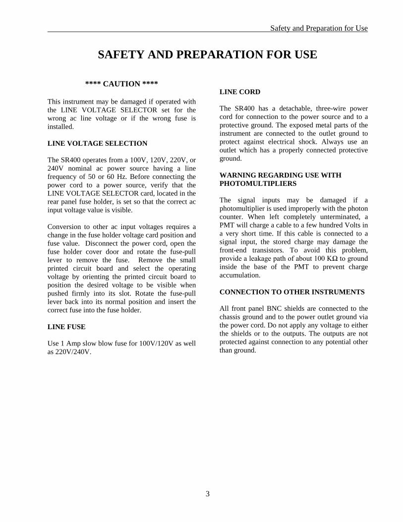
SAFETY AND PREPARATION FOR USE
**** CAUTION **** This instrument may be damaged if operated with the LINE VOLTAGE SELECTOR set for the wrong ac line voltage or if the wrong fuse is installed. LINE VOLTAGE SELECTION The SR400 operates from a 100V, 120V, 220V, or 240V nominal ac power source having a line frequency of 50 or 60 Hz. Before connecting the power cord to a power source, verify that the LINE VOLTAGE SELECTOR card, located in the rear panel fuse holder, is set so that the correct ac input voltage value is visible. Conversion to other ac input voltages requires a change in the fuse holder voltage card position and fuse value. Disconnect the power cord, open the fuse holder cover door and rotate the fuse-pull lever to remove the fuse. Remove the small printed circuit board and select the operating voltage by orienting the printed circuit board to position the desired voltage to be visible when pushed firmly into its slot. Rotate the fuse-pull lever back into its normal position and insert the correct fuse into the fuse holder. LINE FUSE Use 1 Amp slow blow fuse for 100V/120V as well as 220V/240V.
LINE CORD The SR400 has a detachable, three-wire power cord for connection to the power source and to a protective ground. The exposed metal parts of the instrument are connected to the outlet ground to protect against electrical shock. Always use an outlet which has a properly connected protective ground. WARNING REGARDING USE WITH PHOTOMULTIPLIERS The signal inputs may be damaged if a photomultiplier is used improperly with the photon counter. When left completely unterminated, a PMT will charge a cable to a few hundred Volts in a very short time. If this cable is connected to a signal input, the stored charge may damage the front-end transistors. To avoid this problem, provide a leakage path of about 100 KΩ to ground inside the base of the PMT to prevent charge accumulation. CONNECTION TO OTHER INSTRUMENTS All front panel BNC shields are connected to the chassis ground and to the power outlet ground via the power cord. Do not apply any voltage to either the shields or to the outputs. The outputs are not protected against connection to any potential other than ground.
SRS Symbols
4
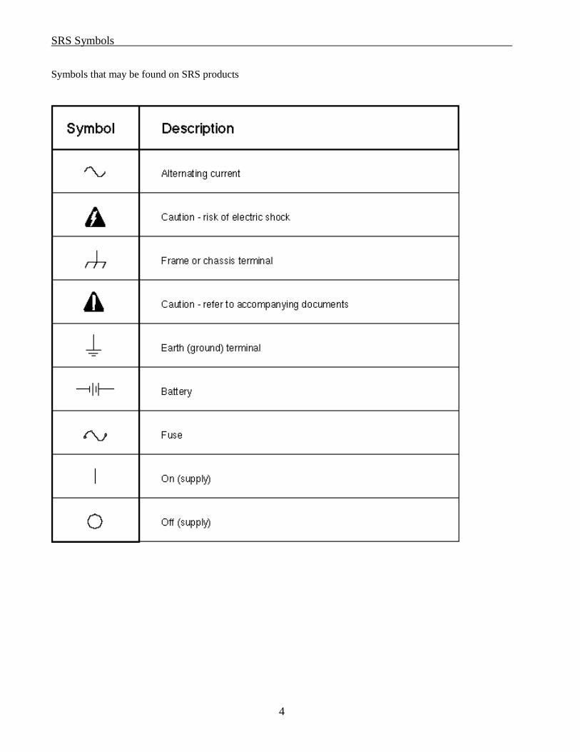
Symbols that may be found on SRS products
SR400 Specifications
5
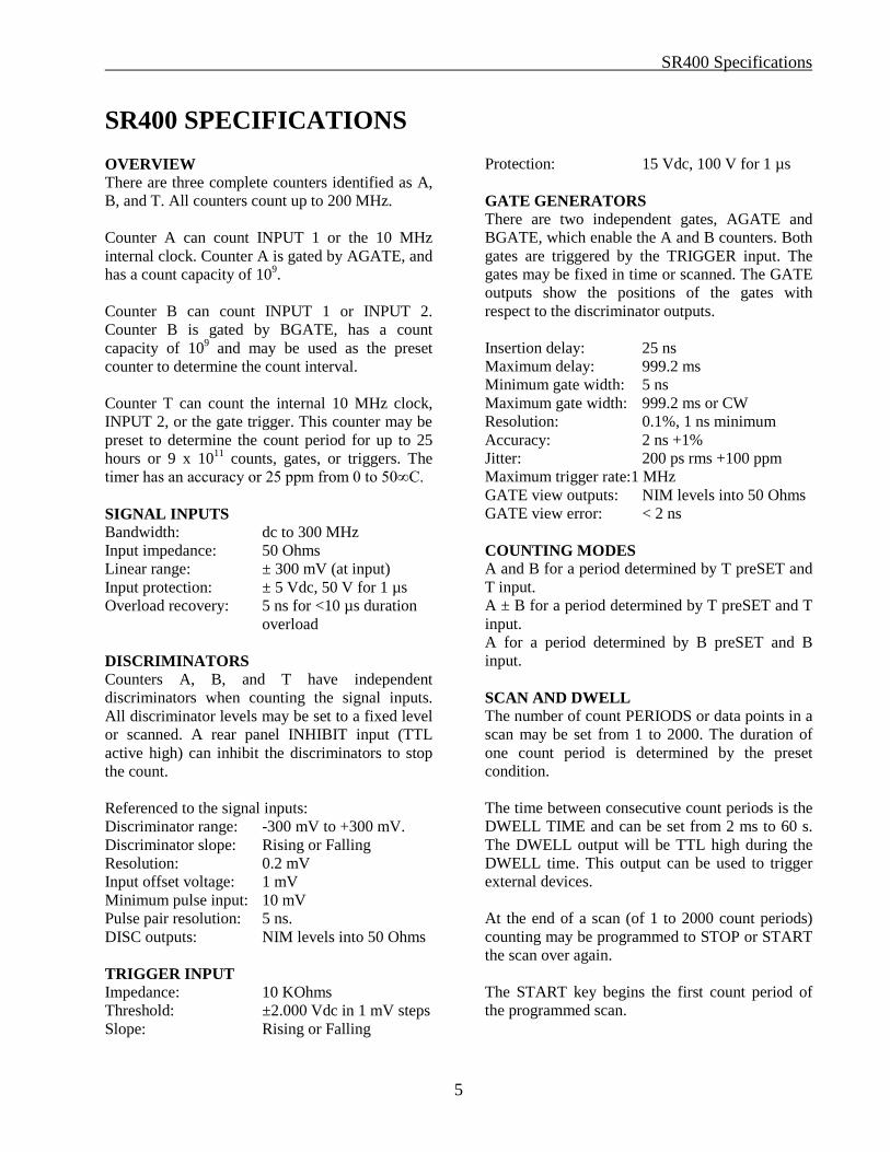
SR400 SPECIFICATIONS OVERVIEW There are three complete counters identified as A, B, and T. All counters count up to 200 MHz. Counter A can count INPUT 1 or the 10 MHz internal clock. Counter A is gated by AGATE, and has a count capacity of 109. Counter B can count INPUT 1 or INPUT 2. Counter B is gated by BGATE, has a count capacity of 109 and may be used as the preset counter to determine the count interval. Counter T can count the internal 10 MHz clock, INPUT 2, or the gate trigger. This counter may be preset to determine the count period for up to 25 hours or 9 x 10¹¹ counts, gates, or triggers. The timer has an accuracy or 25 ppm from 0 to 50∞C. SIGNAL INPUTS Bandwidth: dc to 300 MHz Input impedance: 50 Ohms Linear range: ± 300 mV (at input) Input protection: ± 5 Vdc, 50 V for 1 µs Overload recovery: 5 ns for <10 µs duration
overload DISCRIMINATORS Counters A, B, and T have independent discriminators when counting the signal inputs. All discriminator levels may be set to a fixed level or scanned. A rear panel INHIBIT input (TTL active high) can inhibit the discriminators to stop the count. Referenced to the signal inputs: Discriminator range: -300 mV to +300 mV. Discriminator slope: Rising or Falling Resolution: 0.2 mV Input offset voltage: 1 mV Minimum pulse input: 10 mV Pulse pair resolution: 5 ns. DISC outputs: NIM levels into 50 Ohms TRIGGER INPUT Impedance: 10 KOhms Threshold: ±2.000 Vdc in 1 mV steps Slope: Rising or Falling
Protection: 15 Vdc, 100 V for 1 µs GATE GENERATORS There are two independent gates, AGATE and BGATE, which enable the A and B counters. Both gates are triggered by the TRIGGER input. The gates may be fixed in time or scanned. The GATE outputs show the positions of the gates with respect to the discriminator outputs. Insertion delay: 25 ns Maximum delay: 999.2 ms Minimum gate width: 5 ns Maximum gate width: 999.2 ms or CW Resolution: 0.1%, 1 ns minimum Accuracy: 2 ns +1% Jitter: 200 ps rms +100 ppm Maximum trigger rate:1 MHz GATE view outputs: NIM levels into 50 Ohms GATE view error: < 2 ns COUNTING MODES A and B for a period determined by T preSET and T input. A ± B for a period determined by T preSET and T input. A for a period determined by B preSET and B input. SCAN AND DWELL The number of count PERIODS or data points in a scan may be set from 1 to 2000. The duration of one count period is determined by the preset condition. The time between consecutive count periods is the DWELL TIME and can be set from 2 ms to 60 s. The DWELL output will be TTL high during the DWELL time. This output can be used to trigger external devices. At the end of a scan (of 1 to 2000 count periods) counting may be programmed to STOP or START the scan over again. The START key begins the first count period of the programmed scan.

SR400 Specifications
6
The STOP key terminates the current count period and pauses the scan. If scanning, gates and disc levels are held at their last value. The STOP key pressed while in a paused condition will reset the scan and all scanned parameters will return to their start values. The START key pressed while paused resumes the scan by starting the next count period. The DWELL TIME may also be set to EXTERNAL. In this mode, count periods begin with the START key or EXTERNAL START INPUT (TTL rising edge). Count periods terminate with the preset condition, the STOP key, or the EXTERNAL STOP INPUT (TTL rising edge). A STOP key while not counting resets the scan. This allows completely variable dwell times and/or counting periods. All count data is internally buffered for one scan. Data may be read over the computer interfaces during or after a scan. DISPLAY MODE CONTINUOUS: Displays current counter value HOLD: Displays final count value
D/A OUTPUT The front panel D/A Output is proportional to A, B, A-B, or A+B depending upon the counting mode selected. The D/A output is updated at the end of each count period. There are two rear panel D/A outputs, PORT 1 and PORT 2. These outputs may be set or scanned from the front panel or via the computer interface. Full scale: ± 10 Vdc Resolution: 12 bits (5 mV) Current rating: 10 mA Output Impedance: < 1 Ohm Accuracy: 0.1% + 5 mV COMPUTER INTERFACE IEEE-488 (GPIB) and RS-232 (up to 19.2 kbaud). Full instrument control and data transmission. GENERAL Dimensions: 16" x 13" x 3.5" Weight: 10 lbs Power: 35 Watts from 100, 120,
220, or 240 Vac Warranty: One year parts and labor
on materials and workmanship
Menu Display List
7
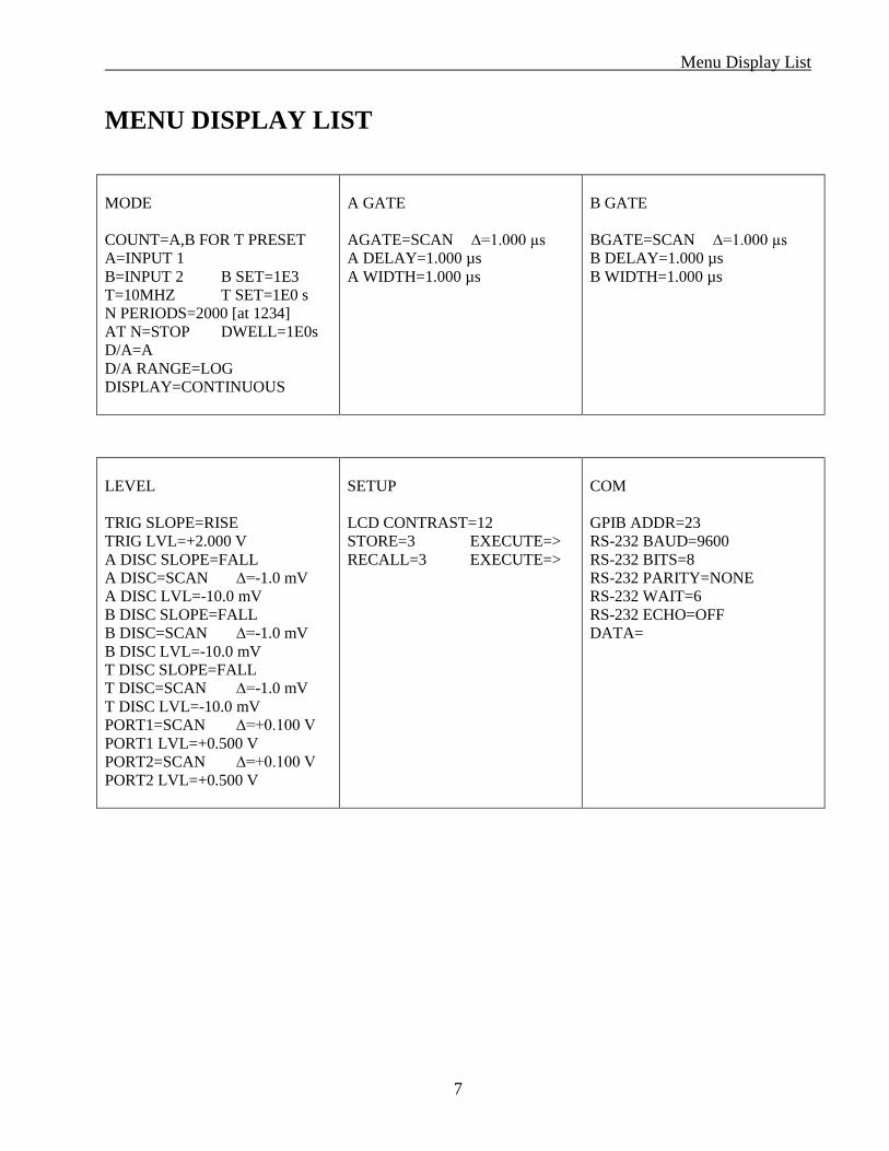
MENU DISPLAY LIST MODE COUNT=A,B FOR T PRESET A=INPUT 1 B=INPUT 2 B SET=1E3 T=10MHZ T SET=1E0 s N PERIODS=2000 [at 1234] AT N=STOP DWELL=1E0s D/A=A D/A RANGE=LOG DISPLAY=CONTINUOUS
A GATE AGATE=SCAN ∆=1.000 µs A DELAY=1.000 µs A WIDTH=1.000 µs
B GATE BGATE=SCAN ∆=1.000 µs B DELAY=1.000 µs B WIDTH=1.000 µs
LEVEL TRIG SLOPE=RISE TRIG LVL=+2.000 V A DISC SLOPE=FALL A DISC=SCAN ∆=-1.0 mV A DISC LVL=-10.0 mV B DISC SLOPE=FALL B DISC=SCAN ∆=-1.0 mV B DISC LVL=-10.0 mV T DISC SLOPE=FALL T DISC=SCAN ∆=-1.0 mV T DISC LVL=-10.0 mV PORT1=SCAN ∆=+0.100 V PORT1 LVL=+0.500 V PORT2=SCAN ∆=+0.100 V PORT2 LVL=+0.500 V
SETUP LCD CONTRAST=12 STORE=3 EXECUTE=> RECALL=3 EXECUTE=>
COM GPIB ADDR=23 RS-232 BAUD=9600 RS-232 BITS=8 RS-232 PARITY=NONE RS-232 WAIT=6 RS-232 ECHO=OFF DATA=

Menu Display List
8
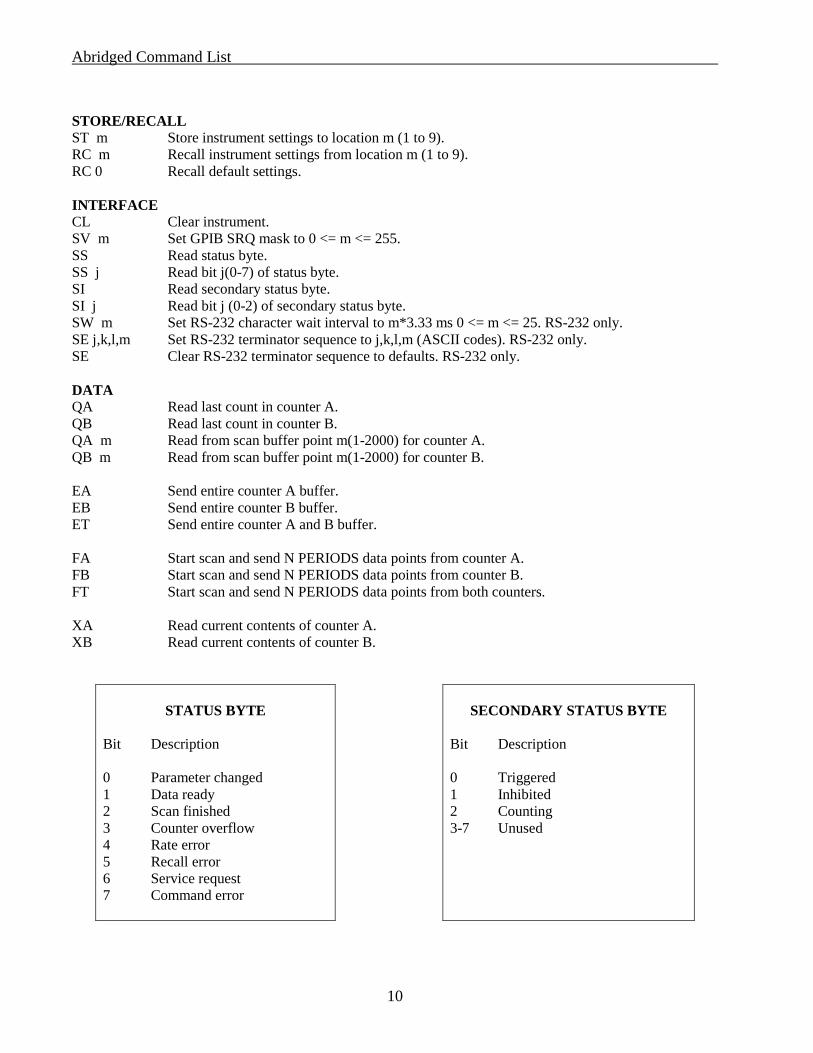
Abridged Command List
9
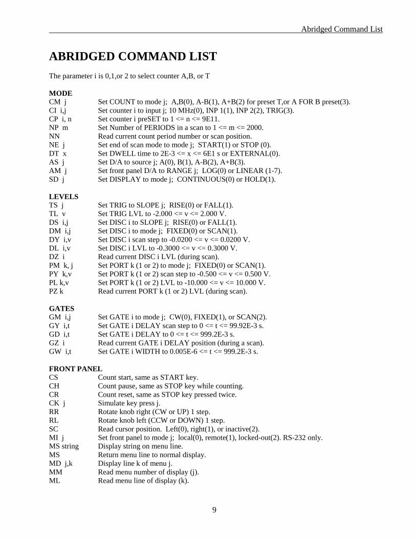
ABRIDGED COMMAND LIST The parameter i is 0,1,or 2 to select counter A,B, or T MODE CM j Set COUNT to mode j; A,B(0), A-B(1), A+B(2) for preset T,or A FOR B preset(3). CI i,j Set counter i to input j; 10 MHz(0), INP 1(1), INP 2(2), TRIG(3). CP i, n Set counter i preSET to 1 <= n <= 9E11. NP m Set Number of PERIODS in a scan to 1 <= m <= 2000. NN Read current count period number or scan position. NE j Set end of scan mode to mode j; START(1) or STOP (0). DT x Set DWELL time to 2E-3 <= x <= 6E1 s or EXTERNAL(0). AS j Set D/A to source j; A(0), B(1), A-B(2), A+B(3). AM j Set front panel D/A to RANGE j; LOG(0) or LINEAR (1-7). SD j Set DISPLAY to mode j; CONTINUOUS(0) or HOLD(1). LEVELS TS j Set TRIG to SLOPE j; RISE(0) or FALL(1). TL v Set TRIG LVL to -2.000 <= v <= 2.000 V. DS i,j Set DISC i to SLOPE j; RISE(0) or FALL(1). DM i,j Set DISC i to mode j; FIXED(0) or SCAN(1). DY i,v Set DISC i scan step to -0.0200 <= v <= 0.0200 V. DL i,v Set DISC i LVL to -0.3000 <= v <= 0.3000 V. DZ i Read current DISC i LVL (during scan). PM k, j Set PORT k (1 or 2) to mode j; FIXED(0) or SCAN(1). PY k,v Set PORT k (1 or 2) scan step to -0.500 <= v <= 0.500 V. PL k,v Set PORT k (1 or 2) LVL to -10.000 <= v <= 10.000 V. PZ k Read current PORT k (1 or 2) LVL (during scan). GATES GM i,j Set GATE i to mode j; CW(0), FIXED(1), or SCAN(2). GY i,t Set GATE i DELAY scan step to 0 <= t <= 99.92E-3 s. GD i,t Set GATE i DELAY to 0 <= t <= 999.2E-3 s. GZ i Read current GATE i DELAY position (during a scan). GW i,t Set GATE i WIDTH to 0.005E-6 <= t <= 999.2E-3 s. FRONT PANEL CS Count start, same as START key. CH Count pause, same as STOP key while counting. CR Count reset, same as STOP key pressed twice. CK j Simulate key press j. RR Rotate knob right (CW or UP) 1 step. RL Rotate knob left (CCW or DOWN) 1 step. SC Read cursor position. Left(0), right(1), or inactive(2). MI j Set front panel to mode j; local(0), remote(1), locked-out(2). RS-232 only. MS string Display string on menu line. MS Return menu line to normal display. MD j,k Display line k of menu j. MM Read menu number of display (j). ML Read menu line of display (k).
Abridged Command List
10
STORE/RECALL ST m Store instrument settings to location m (1 to 9). RC m Recall instrument settings from location m (1 to 9). RC 0 Recall default settings. INTERFACE CL Clear instrument. SV m Set GPIB SRQ mask to 0 <= m <= 255. SS Read status byte. SS j Read bit j(0-7) of status byte. SI Read secondary status byte. SI j Read bit j (0-2) of secondary status byte. SW m Set RS-232 character wait interval to m*3.33 ms 0 <= m <= 25. RS-232 only. SE j,k,l,m Set RS-232 terminator sequence to j,k,l,m (ASCII codes). RS-232 only. SE Clear RS-232 terminator sequence to defaults. RS-232 only. DATA QA Read last count in counter A. QB Read last count in counter B. QA m Read from scan buffer point m(1-2000) for counter A. QB m Read from scan buffer point m(1-2000) for counter B. EA Send entire counter A buffer. EB Send entire counter B buffer. ET Send entire counter A and B buffer. FA Start scan and send N PERIODS data points from counter A. FB Start scan and send N PERIODS data points from counter B. FT Start scan and send N PERIODS data points from both counters. XA Read current contents of counter A. XB Read current contents of counter B.
STATUS BYTE
Bit Description 0 Parameter changed 1 Data ready 2 Scan finished 3 Counter overflow 4 Rate error 5 Recall error 6 Service request 7 Command error
SECONDARY STATUS BYTE
Bit Description 0 Triggered 1 Inhibited 2 Counting 3-7 Unused
Instrument Overview
11
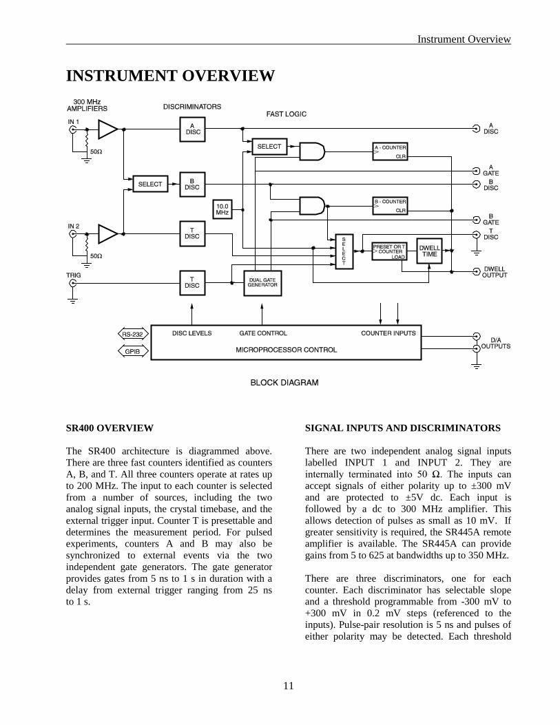
INSTRUMENT OVERVIEW
SR400 OVERVIEW The SR400 architecture is diagrammed above. There are three fast counters identified as counters A, B, and T. All three counters operate at rates up to 200 MHz. The input to each counter is selected from a number of sources, including the two analog signal inputs, the crystal timebase, and the external trigger input. Counter T is presettable and determines the measurement period. For pulsed experiments, counters A and B may also be synchronized to external events via the two independent gate generators. The gate generator provides gates from 5 ns to 1 s in duration with a delay from external trigger ranging from 25 ns to 1 s.
SIGNAL INPUTS AND DISCRIMINATORS There are two independent analog signal inputs labelled INPUT 1 and INPUT 2. They are internally terminated into 50 Ω. The inputs can accept signals of either polarity up to ±300 mV and are protected to ±5V dc. Each input is followed by a dc to 300 MHz amplifier. This allows detection of pulses as small as 10 mV. If greater sensitivity is required, the SR445A remote amplifier is available. The SR445A can provide gains from 5 to 625 at bandwidths up to 350 MHz. There are three discriminators, one for each counter. Each discriminator has selectable slope and a threshold programmable from -300 mV to +300 mV in 0.2 mV steps (referenced to the inputs). Pulse-pair resolution is 5 ns and pulses of either polarity may be detected. Each threshold
Instrument Overview
12
may be programmed to scan in either direction with selectable step size. COUNTING Each counter's input may be selected from a number of sources. All multiplexing of counter inputs is done internally to provide accurate timing and ease of operation. Input cables should rarely need to be swapped or disconnected to change measurement modes. The actual inputs to the counters can be viewed as NIM level pulses from the DISC outputs on the front panel. The DISC pulses are negative going from 0 to -0.7 V. The falling edge is the active or counted edge regardless of the discriminator slope setting. The DISC outputs are very useful when adjusting discriminator thresholds or gate timing. When the START key is pressed, a START command is received from the computer interface, or the EXTERNAL START input is pulsed, counter T is enabled to count. The COUNT PERIOD begins with the first pulse from T counter's input after START. The COUNT PERIOD enables counters A and B to count their respective inputs. If the A GATE and B GATE are CW or continuous, all pulses that occur during the COUNT PERIOD are counted. If the gates are enabled, only the pulses that occur during those gates which fall within the COUNT PERIOD are counted. Counter T is presettable from 1 to 9E11. When counter T reaches the preset count, the COUNT PERIOD is terminated and counting is halted on all counters. When the input to counter T is the 10 MHz crystal timebase, the COUNT PERIOD is a fixed time interval from 100 ns to 25 hours. When the input is INPUT 2, the COUNT PERIOD is externally determined and can be as short as 5 ns and indefinitely long. This mode is used for source compensation or reciprocal measurements. If the input is TRIGGER, the COUNT PERIOD is a fixed number of gates (each trigger provides one gate). This results in a constant gate aperture time during each COUNT PERIOD. N+1 Triggers are required for N gates per period. If the input is B PRESET, then counter T counts the B DISC
output gated by B GATE. This is for gated ratio or reciprocal counting. The SR400 may be programmed to cycle through 1 to 2000 COUNT PERIODS in a single scan. At the end of the programmed scan, the counters may be stopped or the scan may be restarted. If the end of scan mode is STOP, then after the last COUNT PERIOD in the scan, the counters are halted indefinitely. A counter RESET is required to rearm the counters and a START command starts another scan. If the Number of PERIODS in the scan is 1, then each START command results in one COUNT PERIOD. If N PERIODS is greater than 1, then consecutive COUNT PERIODS are separated by the DWELL time. The DWELL time may be set from 2 ms to 60 s. During the DWELL time, counting is disabled and data may be transferred or external parameters scanned. The DWELL OUTPUT is a TTL output which is high during the DWELL time. At the end of the DWELL time, the next COUNT PERIOD begins and the scan continues until N PERIODS have been measured. If the end of scan mode is START, one DWELL time separates the last COUNT PERIOD of the completed scan and the first COUNT PERIOD of the next scan. Another DWELL mode is EXTERNAL. In this mode, the EXTERNAL START input enables counter T. The COUNT PERIOD begins with the first pulse to counter T after START. Counting then proceeds normally until the preset is reached. At the end of the preset COUNT PERIOD, the DWELL time is indefinite and the next COUNT PERIOD starts with the next EXTERNAL START pulse. In this way, preset COUNT PERIODS may be synchronized to external events. If externally determined COUNT PERIODS are desired, then the preset COUNT PERIOD can be set to a value much larger than actually required and the EXTERNAL STOP input used to terminate the COUNT PERIOD. The COUNT PERIOD then starts with the first pulse to counter T after EXTERNAL START and ends with EXTERNAL STOP. The next EXTERNAL START begins the next COUNT PERIOD in the scan. When the scan is finished and the scan end mode is STOP, a RESET from the front panel or computer interface is required to reset the scan. If the scan end mode
Instrument Overview
13
is START, the next EXTERNAL START begins the first COUNT PERIOD of the next scan. SCANNING In all scan modes, a number of parameters may be scanned. These parameters are the three discriminator thresholds (Pulse Height Analysis), the two gate delays (Boxcar mode), and the two D/A output ports (X-axis of recorder, scope, or analog control of other apparatus). After each COUNT PERIOD, each scanning parameter is adjusted by one step. All changes are made during the DWELL time so that all values are stable during the COUNT PERIODS. The scan limits are determined by the start position, the step size, and the number of PERIODS in a scan. The range of a scan is N PERIODS times the step size. When the counters are reset, all scanned parameters return to their start positions. GATING The gate generators may be disabled by setting the gate modes to CW. In this mode, the gates are continuously open and counting is enabled solely by the COUNT PERIOD. This is appropriate for CW sources or long counting intervals. If the signal is pulsed or so weak that synchronous (lock-in) measurement is required, then the gate generators are required. The gates prevent pulses that occur outside the time interval of interest from being counted and improve signal to noise ratio. When the gates are scanned, the time behavior of the signal may be recovered. The gates are triggered by the TRIGGER input. The TRIGGER threshold is adjustable from -2V to +2V and slope may be either RISE or FALL. The discriminated trigger pulse may be viewed through the T DISC output when the input to counter T is set to TRIG. This can be helpful when setting the trigger threshold. The minimum insertion delay from trigger to gate is 25 ns. The additional delay may be programmed from 0 ns to 999.2 ms with a resolution of 1 part in 1000 or 1 ns, whichever is greater. The gate width is adjustable from 5 ns to 999.2 ms with the same resolution. The two gates are output as NIM pulses
from the GATE outputs. The gates are open when the outputs are low. The gate outputs have a timing accuracy with respect to the discriminator outputs of 2 ns. This allows accurate timing of fast gates relative to the signal. The two gates have independent modes, delays, and widths. This allows for a variety of measurements. For example: 1) "Boxcar" mode. The gates are used to enable the counters only when the signal is present. If the gates are scanned, then the time profile of the signal is recovered. Background subtraction can be included by using one gate for the signal and an equal width gate on the background, either before or after the signal. The signal gate may be scanned while the background gate held fixed. Gated source compensation is also possible since counters A and B may count different sources at the same time or the same source at different times. In the compensation mode, the COUNT PERIOD is determined by the gated output of the B discriminator and the COUNT MODE is A FOR B PRESET. 2) "Lock-in" or "Chopped" mode. In this case, a cw signal is chopped on and off. This can be accomplished with a light chopper such as the SR540. The light chopper reference output is used to trigger the gates. The A GATE is positioned during the "open" cycle and counts signal plus noise. The B GATE is positioned during the "closed" cycle and only counts the noise. The counter outputs are subtracted to give only the signal. The widths of both gates should be equal and less than half of the chopper period. This prevents frequency jitter in the chopper from affecting the overlap of the gates with the open and close cycles of the chopper. When counter T is preset and its input is set to TRIG, then each COUNT PERIOD consists of a constant number of gates. N+I triggers are needed for N gates per preiod. This is the usual mode of gated operation. However, a number of other modes are available. For example, if the input is set to 10 MHz, each COUNT PERIOD consists of the number of gates which occur during the COUNT PERIOD time interval. If the input is a signal input, then counting is both gated and
Instrument Overview
14
source compensated. If the DWELL mode is EXTERNAL, an EXTERNAL START pulse starts counting and an EXTERNAL STOP pulse stops counting. The counters are enabled only during those gates which occurred between the two EXTERNAL pulses. COUNT MODES The length of a COUNT PERIOD is the time it takes counter T to reach its preset count. If Nt is the preset count in counter T, and Ra and Rt are the mean pulse rates of the inputs to counters A and T, then the COUNT PERIOD is T = Nt / Rt The number of counts in counter A will be A = Ra T = Ra Nt / Rt Rate: If Rt = 10 MHz, then the COUNT PERIOD is a constant amount of time and A = Ra ( Nt / Rt ) ~ Ra and counter A measures the mean rate of its input. Gated: If Rt is the gate trigger rate and counter A is gated, then the COUNT PERIOD is Nt/Rt but the "effective" time the counter is enabled is NtWa where Wa is the width of A gate and A = Ra ( Nt Wa ) ~ Ra In this case, counter A measures the mean rate during the A gate. Source Compensated: If Rt is INPUT 2, then the COUNT PERIOD is determined by the pulse rate of INPUT 2 and the T discriminator. Count A will be A = Nt Ra / Rt ~ Ra / Rt and is proportional to the ratio of the rates of counters A and T. If INPUT 2 monitors source
intensity, then the COUNT PERIOD will adjust for fluctuations in the source. Counter A measures the ratio of its mean input rate and the mean rate of INPUT 2. Reciprocal: If Rt is INPUT 2, then the COUNT PERIOD is Nt/Rt. If Ra is 10 MHz, then counter A measures A = Ra Nt / Rt = ( Ra Nt ) / Rt ~ 1 / Rt and is proportional to the reciprocal of the count rate of INPUT 2. Note that each COUNT PERIOD is determined by Nt counts of INPUT 2, thus the measurement time is determined by the signal strength. Measurements of both strong and weak signals are made to the same accuracy for constant signal to noise ratio. Counter B: Counter B may be used in all of the above modes except Reciprocal. Since counter B is completely independent of counter A, 2 sources of counts may be measured simultaneously. These sources may be the same signal or 2 different signals; the sources may be discriminated at separate thresholds; they may be non-gated or gated; if gated, the 2 gates may be independently set. Almost any measurement can be made. In addition, counter B has a preset mode called A FOR B PRESET. In this mode, the input to counter B is sent to counter T. The COUNT PERIOD is now determined by the B discriminator and the B gate. If Ra is INPUT 1, then counter A is source compensated by the gated input of counter B. This allows source compensation of gated signals and sources. If Ra is 10 MHz, then counter A measures the reciprocal of the rate of counter B's gated input. OUTPUTS The front panel can display counts up to 109 - 1. Counters A and B can be displayed as separate counters or combined as A-B or A+B. When A FOR B PRESET is the count mode, then only A data is displayed.
Instrument Overview
15
The front panel D/A output provides an analog output proportional to A, B, A-B, or A+B depending on the counting mode. The scale may be logarithmic (1V/decade) or linear to any 3 digits. If a chart recorder is used, the D/A output should drive the Y axis. The X axis can be recorder driven (strip chart mode) or the PORT1 or PORT2 outputs can be used to drive the X axis (scans). This latter method allows accurate determination of the X value of each point. If the DWELL output is used as the pen lift, the points will be unconnected. If count rates are high and count periods short, then scans may be displayed on an X-Y scope. The D/A output is the Y drive and PORT1 or PORT2 is the X drive. The DWELL output should be used as the blanking pulse.

Instrument Overview
16

Measurement Examples
17
MEASUREMENT EXAMPLES Example 1: Internally Triggered Gate Mode This example, described under the heading “QUICK TEST” on page 59 of this manual, is easy to perform and will quickly acquaint the user with the basic operation of the SR400. Example 2: Externally Triggered Gate Mode In this example, the SR400 is programmed to make 10 counting measurements of a 10 kHz pulse train. For each measurement, a gate will be delayed 500 ms from an external trigger pulse and will open of 500 ms duration. Following the gate, there will be a 6 second dwell period* during which the counter will be disarmed. After the dwell period, the counter will reset to 0 counts, re-arm and repeat the measurement. After 10 measurement cycles, the SR400 will stop counting and disarm. You will need a 10 kHz signal source and a 0.5 Hz square wave generator for this example. *It is important to note that the dwell period begins at the first external trigger pulse arriving after the gate is closed. Thus, even though there is only one gate opened for each measurement cycle, a minimum of two external triggers are needed: one to trigger the gate and another to begin the dwell period. The following timing diagram illustrates this example.
Measurement Examples
18
1. Turn the SR400 off. Hold down the STOP (RESET) button while turning the SR400 on. Wait three seconds and release the button. 2. Press the MODE key. Using the four arrow keys and the front panel knob, select the following parameters. Unless otherwise indicated, leave all other settings at their default values: T = TRIG TSET = 1E0 N PERIODS = 10 [AT 0] AT N = STOP DWELL = 6E0 S 3. Press the A GATE key and select the following parameters: A GATE = FIXED A DELAY = 500 mS A width = 500 mS 4. Press the LEVEL key and select the following parameters: A DISC SLOPE = RISE A DISC LVL = +150 mV 5. Using a function generator or a pulse generator, apply a 0.5 Hz, 5 V (TTL) signal to the TRIGGER INPUT on the SR400. 6. Using a second signal source, apply a 10 kHz square wave (or pulse train) with an amplitude of approximately 500 mV to the SIGNAL INPUT 1 on the SR400. 7. To view the COUNT PERIODS, press the MODE key and use the up/down arrow keys to display “N PERIODS = 10 [at 0]” Arm the counter by pressing the START button. (Alternatively, a TTL pulse applied to the START BNC on the front panel will arm the counter.) Each measurement cycle should result in approximately 5,000 counts. As an extension of the above example, the SR400 can be programmed to accumulate counts over numerous gates. This is often done to improve the signal to noise ratio of low light level experiments. To accumulate counts, set TSET (MODE menu) to the desired number of gates. For example, if you wish to accumulate over five gates, set TSET – 5E0. In this case, six external triggers are required for each measurement cycle: five to trigger the five gates and one to start the DWELL PERIOD. Any additional triggers received during the DWELL PERIOD are ignored.
Measurement Examples
19
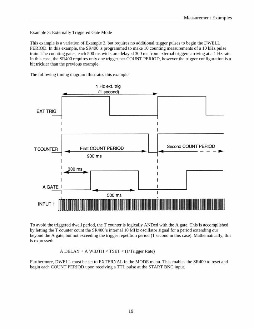
Example 3: Externally Triggered Gate Mode This example is a variation of Example 2, but requires no additional trigger pulses to begin the DWELL PERIOD. In this example, the SR400 is programmed to make 10 counting measurements of a 10 kHz pulse train. The counting gates, each 500 ms wide, are delayed 300 ms from external triggers arriving at a 1 Hz rate. In this case, the SR400 requires only one trigger per COUNT PERIOD, however the trigger configuration is a bit trickier than the previous example. The following timing diagram illustrates this example.
To avoid the triggered dwell period, the T counter is logically ANDed with the A gate. This is accomplished by letting the T counter count the SR400’s internal 10 MHz oscillator signal for a period extending our beyond the A gate, but not exceeding the trigger repetition period (1 second in this case). Mathematically, this is expressed:
A DELAY + A WIDTH < TSET < (1/Trigger Rate) Furthermore, DWELL must be set to EXTERNAL in the MODE menu. This enables the SR400 to reset and begin each COUNT PERIOD upon receiving a TTL pulse at the START BNC input.

Measurement Examples
20
1. Turn the SR400 off. Hold down the STOP (RESET) button while turning the SR400 on. Wait three seconds and release the button. 2. Press the MODE key. Using the four arrow keys and the front panel knob, select the following parameters. Unless otherwise indicated, leave all other settings at their default values: T = 10 MHz TSET = 9E-1 s N PERIODS = 10 [AT 0] AT N = STOP DWELL = EXTERNAL (Turn the knob counterclockwise until “DWELL = EXTERNAL” is displayed.) 3. Press the A GATE key and select the following parameters: A GATE = FIXED A DELAY = 300 mS A width = 500 mS 4. Press the LEVEL key and select the following parameters: A DISC SLOPE = RISE A DISC LVL = +150 mV 5. Using a function generator or a pulse generator, apply a 1 Hz, 5 V (TTL) signal to the EXTERNAL START input on the SR400. Use a BNC ‘T; connector at the EXTERNAL START input and extend a cable from the EXTERNAL START input to the TRIG input. 6. Using a second signal source, apply a 10 kHz square wave (or pulse train) with an amplitude of approximately 500 mV to the SIGNAL INPUT 1 on the SR400. 7. To view the COUNT PERIODS, press the MODE key and use the up/down arrow keys to display “N PERIODS = 10 [at 0]” 8. Arm the SR400 by pressing the STOP (RESET) button. Each counting period should result in approximately 5,000 counts. After 10 counting measurements the SR400 will disarm. To re-arm, press the STOP (RESET) button.
Guide to Operation
21
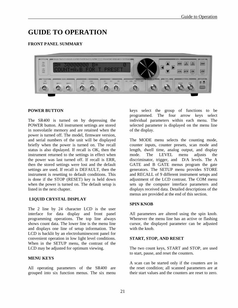
GUIDE TO OPERATION FRONT PANEL SUMMARY
POWER BUTTON The SR400 is turned on by depressing the POWER button. All instrument settings are stored in nonvolatile memory and are retained when the power is turned off. The model, firmware version, and serial numbers of the unit will be displayed briefly when the power is turned on. The recall status is also dipslayed. If recall is OK, then the instrument returned to the settings in effect when the power was last turned off. If recall is ERR, then the stored settings were lost and the default settings are used. If recall is DEFAULT, then the instrument is resetting to default conditions. This is done if the STOP (RESET) key is held down when the power is turned on. The default setup is listed in the next chapter. LIQUID CRYSTAL DISPLAY The 2 line by 24 character LCD is the user interface for data display and front panel programming operations. The top line always shows count data. The lower line is the menu line and displays one line of setup information. The LCD is backlit by an electroluminescent panel for convenient operation in low light level conditions. When in the SETUP menu, the contrast of the LCD may be adjusted for optimum viewing. MENU KEYS All operating parameters of the SR400 are grouped into six function menus. The six menu
keys select the group of functions to be programmed. The four arrow keys select individual parameters within each menu. The selected parameter is displayed on the menu line of the display. The MODE menu selects the counting mode, counter inputs, counter presets, scan mode and length, dwell time, analog output, and display mode. The LEVEL menu adjusts the discriminator, trigger, and D/A levels. The A GATE and B GATE menus program the gate generators. The SETUP menu provides STORE and RECALL of 9 different instrument setups and adjustment of the LCD contrast. The COM menu sets up the computer interface parameters and displays received data. Detailed descriptions of the menus are provided at the end of this section. SPIN KNOB All parameters are altered using the spin knob. Whenever the menu line has an active or flashing cursor, the displayed parameter can be adjusted with the knob. START, STOP, AND RESET The two count keys, START and STOP, are used to start, pause, and reset the counters. A scan can be started only if the counters are in the reset condition; all scanned parameters are at their start values and the counters are reset to zero.
Guide to Operation
22
In general, pressing the STOP key twice in succession puts the counters into the reset condition. START begins the first COUNT PERIOD of the programmed scan. If the DWELL time is programmed, then the scan will continue automatically. A STOP will pause the scan; the current COUNT PERIOD is terminated and ignored. A START while paused will resume the scan. A STOP while paused resets the scan. If the DWELL time is EXTERNAL, then a STOP during the COUNT PERIOD terminates the COUNT PERIOD and advances the scan. START begins the next COUNT PERIOD in the scan. A START during a COUNT PERIOD or programmed DWELL period is ignored. A STOP while in a dwell period or pause resets the scan; all scanned parameters return to their start values and the counters are reset. In general, 2 consecutive presses of the STOP key will reset the counters. The SCAN led is on when a scan is in progress. The SCAN led is off when the scan is paused or the counters are reset. INSTRUMENT STATUS Six LED's indicate the instrument status. REM is on when the front panel is locked out, ACT flashes when there is activity on the computer interfaces, and ERR flashes when there is a computer interface error. COUNT is on during each COUNT PERIOD, OVRN indicates that a counter has exceeded 109 - 1 counts during a COUNT PERIOD, and RATE flashes whenever a gate delay or width exceeds the trigger period minus 1 µs. The RATE led also flashes if the trigger rate exceeds 1 MHz, even if the gates are in the CW mode. COUNTER LED'S The source LED's in the counter sections indicate what each counter's input is. The counter inputs are output through the DISC outputs. The SET LED's indicate which counter, B or T, is the preset counter. The B SET LED is on when the mode is
A FOR B PRESET, the T SET LED is on otherwise. INPUTS The rising or falling edge of the TRIGGER input triggers the gate generators. The input impedance is 10 KΩ and the minimum pulse width is 10 ns. The trigger level is adjustable from -2V to +2V with either slope. The minimum pulse amplitude is 0.1 V. The SIGNAL INPUTS, 1 and 2, are 50 Ω analog inputs. Photomultiplier or preamplifier outputs are connected to these inputs. These inputs are linear between -300 mV to +300 mV and protected to ± 5 Vdc. EXTERNAL START is a TTL input with the rising edge active. The minimum pulse width is 20 ns. When the DWELL time is EXTERNAL, the COUNT PERIOD begins with the rising edge of START and ends with the preset condition or the rising edge of STOP. When the DWELL time is programmed, EXT START begins the scan. EXTERNAL STOP is a TTL input with the rising edge active. The minimum pulse width is 20 ns. When the DWELL time is EXTERNAL, EXT STOP ends each count period. Reset must be accomplished via the STOP key or computer interface. When the DWELL time is programmed, EXT STOP resets the scan. OUTPUTS The DISC outputs are 50 Ω, NIM level, outputs showing the actual inputs to the three counters. These outputs are active low (-.7 V) and counting occurs on the falling edge. The outputs are low when the signal inputs exceed their threshold levels with the correct slope. Cables attached to the DISC outputs should be kept far from the cables which carry the SIGNAL inputs. The 0.7 V DISC pulses can be picked up by the SIGNAL cables and discriminated. This causes the discriminators to oscillate. This is not a problem if the threshold is greater than 10 mV. If smaller thresholds are required, careful arrangement of the cables is necessary, or the
Guide to Operation
23
DISC output should just be terminated at the front panel. The GATE outputs are 50 Ω, NIM level, outputs showing the actual gates to counters A and B. The GATE outputs are low (-.7 V) during the gate. The timing accuracy between the GATE outputs and DISC outputs is 2 ns. The D/A analog output provides a -10V to +10V output proportional to the count data with linear or logarithmic scaling. Output impedance is < 1 Ω and the maximum current output is 10 mA. The DWELL output is a TTL level output which is high whenever the counters are paused. The rising edge may be used to trigger changes in external parameters or data acquisition.
Guide to Operation
24
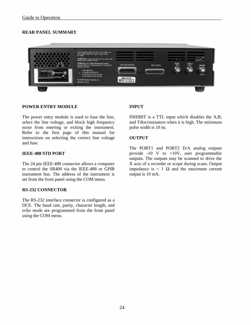
REAR PANEL SUMMARY
POWER ENTRY MODULE The power entry module is used to fuse the line, select the line voltage, and block high frequency noise from entering or exiting the instrument. Refer to the first page of this manual for instructions on selecting the correct line voltage and fuse. IEEE-488 STD PORT The 24 pin IEEE-488 connector allows a computer to control the SR400 via the IEEE-488 or GPIB instrument bus. The address of the instrument is set from the front panel using the COM menu. RS-232 CONNECTOR The RS-232 interface connector is configured as a DCE. The baud rate, parity, character length, and echo mode are programmed from the front panel using the COM menu.
INPUT INHIBIT is a TTL input which disables the A,B, and Tdiscriminators when it is high. The minimum pulse width is 10 ns. OUTPUT The PORT1 and PORT2 D/A analog outputs provide -10 V to +10V, user programmable outputs. The outputs may be scanned to drive the X axis of a recorder or scope during scans. Output impedance is < 1 Ω and the maximum current output is 10 mA.
Guide to Operation - Menus
25
FRONT PANEL MENUS The lower line of the LCD display is the menu line. Menu lines are grouped into six menus. To select a new group or menu, press a new menu key. The menu line that will be displayed is the most recently active menu line of the new menu. Each menu contains several lines. Each line may consist of 1 or 2 displayed parameters. The DOWN and UP keys change which menu line within a menu will be displayed. The DOWN key displays the next menu line and the UP key, the previous line. Pressing either key many times in succession will scroll through all of the menu lines within a menu. If the menu line contains two parameters, the LEFT and RIGHT keys select between the two. On some lines, the right hand parameter is active only for certain values of other parameters. On these lines, the right hand parameter may be inactive. The spin knob is used to modify the active parameter. A flashing cursor precedes the value which the knob will alter. The following section details each menu line. The lines are listed in the order in which the DOWN key scrolls through each menu. For parameters with limited choices, all selections are shown. For numerical parameters, example values are shown.
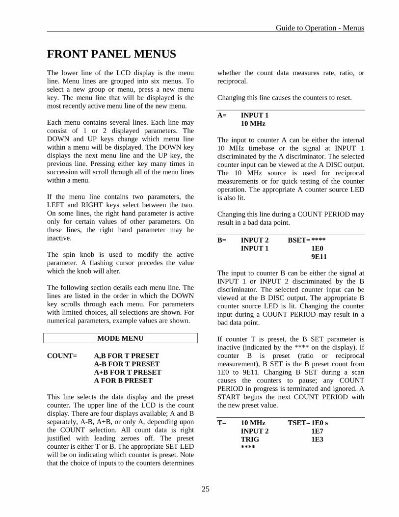
MODE MENU COUNT= A,B FOR T PRESET A-B FOR T PRESET A+B FOR T PRESET A FOR B PRESET This line selects the data display and the preset counter. The upper line of the LCD is the count display. There are four displays available; A and B separately, A-B, A+B, or only A, depending upon the COUNT selection. All count data is right justified with leading zeroes off. The preset counter is either T or B. The appropriate SET LED will be on indicating which counter is preset. Note that the choice of inputs to the counters determines
whether the count data measures rate, ratio, or reciprocal. Changing this line causes the counters to reset. A= INPUT 1 10 MHz The input to counter A can be either the internal 10 MHz timebase or the signal at INPUT 1 discriminated by the A discriminator. The selected counter input can be viewed at the A DISC output. The 10 MHz source is used for reciprocal measurements or for quick testing of the counter operation. The appropriate A counter source LED is also lit. Changing this line during a COUNT PERIOD may result in a bad data point. B= INPUT 2 BSET= **** INPUT 1 1E0 9E11 The input to counter B can be either the signal at INPUT 1 or INPUT 2 discriminated by the B discriminator. The selected counter input can be viewed at the B DISC output. The appropriate B counter source LED is lit. Changing the counter input during a COUNT PERIOD may result in a bad data point. If counter T is preset, the B SET parameter is inactive (indicated by the **** on the display). If counter B is preset (ratio or reciprocal measurement), B SET is the B preset count from 1E0 to 9E11. Changing B SET during a scan causes the counters to pause; any COUNT PERIOD in progress is terminated and ignored. A START begins the next COUNT PERIOD with the new preset value. T= 10 MHz TSET= 1E0 s INPUT 2 1E7 TRIG 1E3 ****

Guide to Operation - Menus
26
The input to counter T can be the internal 10 MHz timebase (rate measurement), the signal at INPUT 2 discriminated by T discriminator (ratio or reciprocal measurement), or the TRIGGER input discriminated by the trigger discriminator (constant gate aperture). The selected counter input can be viewed at the T DISC output. The appropriate T counter source LED is lit. If counter B is preset, this line is inactive (indicated by the **** on the display). If counter T is preset, both parameters on this line are active. T SET is the preset value of counter T from 1E0 to 9E11. If the T input is 10 MHz, then T SET is displayed as real time = T SET cycles of 10 MHz. ChangingT SET during a scan causes the counters to pause; any COUNT PERIOD in progress is terminated and ignored. A START begins the next COUNT PERIOD with the new preset value. N PERIODS=2000 [at 1234] This line programs the number of COUNT PERIODS in one scan from 1 to 2000. N PERIODS determines the length of the internal data buffer and the range of any scanned parameters. The quantity in brackets is the number of completed COUNT PERIODS in the current scan. Changing N PERIODS during a scan changes the length of the current scan. Reducing N PERIODS past the current scan position will cause an end of scan condition. AT N= STOP DWELL= 1E0 s START 2E-3 s EXTERNAL This line sets the end of scan mode and the DWELL time. When a scan reaches N PERIODS, the counters may be paused or restarted. AT N=STOP causes an end of scan pause. All scanned parameters are held at their final values. A counter reset is required before another scan can begin. If N PERIODS is 1, then each START results in one COUNT PERIOD. If N PERIODS is greater than 1, then consecutive COUNT PERIODS are separated by the DWELL time. During the DWELL time, counting is disabled and scanned
parameters updated. The DWELL OUTPUT is TTL high during the DWELL time. If AT N=START, the counters will wait one DWELL time at the end of each scan, during which all scanned parameters return to their start positions, and then another scan begins. This is used for continuous data taking with the measurement rate determined by the COUNT PERIOD plus the DWELL TIME. The DWELL time may be programmed from 2E-3 s to 6E1 s (1 minute) or set to EXTERNAL. The internal DWELL time is based on the 10 MHz timebase and may have 200 ns of indeterminacy. Changing the DWELL time during a scan causes the counters to pause; any COUNT PERIOD in progress is terminated and ignored. Setting the DWELL time below 2E-3 s results in an EXTERNAL dwell. In this mode, the START key, EXT START, or remote start command starts the COUNT PERIOD. The COUNT PERIOD lasts until the preset condition is reached. The following DWELL time is indefinite; the next COUNT PERIOD begins with another START. A STOP key, EXT STOP, or remote stop command during the COUNT PERIOD terminates the COUNT PERIOD. Thus by programming the preset COUNT PERIOD much longer than required, the COUNT PERIOD may be determined by START and STOP. Scanning proceeds as normal. NOTE: If AT N=STOP, the counters will pause at the end of a scan. A reset (STOP key, EXT STOP, or remote reset command) is required to rearm the counters before another scan can begin. In general, to reset the counters at any time, the STOP key is pressed twice in succession. D/A= A B A+B A-B The D/A output is proportional to the count data on the top line of the LCD. When the COUNT is A-B, A+B, or A only, the D/A output can only follow the data display. In these modes, the cursor is inactive and the knob does nothing. If the
Guide to Operation - Menus
27
COUNT is A,B FOR T PRESET, then the D/A output can follow either A or B. D/A RANGE= LOG ##765#### The D/A output scale can be either logarithmic or linear. If the output is logarithmic, the scale is 1V per decade with 1 count being 0V, 0 counts being -1V, and negative counts being -2V. If the scale is linear, the output is proportional to 3 digits of the count. These digits are shown while the ignored digits are represented by #'s. The D/A output is updated at the end of each COUNT PERIOD. If the D/A output is driving a chart recorder, the end of scan mode should be STOP or the pen reset will mar the graph. If the DWELL output is connected to the recorder pen lift, data will be plotted as unconnected points, otherwise, the discrete points will be connected. DISPLAY= CONTINUOUS HOLD The count data on the upper line of the LCD can be updated in two ways. CONTINUOUS mode updates the display 20 times a second during the COUNT PERIOD. Data is held during the DWELL time at the final value reached during the previous COUNT PERIOD. HOLD updates the display only at the end of each COUNT PERIOD. CONTINUOUS is useful when COUNT PERIODS are long, HOLD is better when COUNT PERIODS are short.
LEVEL MENU TRIG SLOPE= RISE FALL The gate generator may be triggered on either the rising or falling edge of the TRIGGER input. TRIG LVL=+2.000 V The gate TRIGGER threshold level may be adjusted from -2.000 V to +2.000V. The
discriminated trigger pulses may be viewed through the T DISC output when counter T is preset and its input is TRIG. This can be helpful in selecting a trigger level. The minimum pulse amplitude required to trigger is 100 mV. A DISC SLOPE= RISE FALL When A counter's input is INPUT 1, A discriminator may be triggered by rising or falling edges of the INPUT 1 signal. If the signal pulses are negative going, then the slope should be FALL. If the signal pulses are positive, then the slope should be RISE. In either case, the A DISC output is always active low; i.e., a discriminated rising edge of the signal will be output as a negative going NIM pulse at the A DISC output. The falling edges of the A DISC output are counted by counter A. A DISC= FIXED SCAN ∆= -1.0 mV The threshold level of A discriminator may be FIXED or SCANned. If the level is fixed, the right hand parameter is not displayed. If the level is scanned, then the right hand parameter is the step size. At the end of each count period in a scan, the level is incremented by one step size. The step size can be varied from -20.0 mV to + 20.0 mV. The range of a scan is N PERIODS times the step size. The starting level is set in the next menu line. The scan mode may be changed during a scan. If it is changed to SCAN, the level begins scanning from the start value on the next count period. If it is changed to FIXED, the level returns to the start level immediately. The step size may also be changed during a scan. The new step size will be in effect at the end of the next count period. The scan is not reset or paused. A DISC LVL = -10.0 mV
: -11.0 mV The threshold level of A discriminator may be adjusted from -300 mV to + 300 mV. This level is
Guide to Operation - Menus
28
the fixed threshold when A DISC is FIXED and the starting level when A DISC is SCANned. When the A DISC mode is SCAN and a scan is in progress, this line displays the current position of the A DISC level. The cursor is inactive and replaced by a ':'. The spin knob cannot adjust the threshold while it is scanning. When the mode is SCAN, the starting level may only be adjusted when the counters are in reset. B DISC SLOPE= RISE FALL B discriminator may be triggered by rising or falling edges of the INPUT 1 or INPUT 2 signal. If the signal pulses are negative going, then the slope should be FALL. If the signal pulses are positive, then the slope should be RISE. In either case, the B DISC output is always active low; i.e., a discriminated rising edge of the signal will be output as a negative going NIM pulse at the B DISC output. The falling edges of the B DISC output are counted by counter B. B DISC= FIXED
SCAN ∆= -1.0 mV The threshold level of B discriminator may be FIXED or SCANned. If the level is FIXED, the right hand parameter is not displayed. If the level is scanned, then the right hand parameter is the step size. At the end of each count period in a scan, the level is incremented by one step size. The step size can be varied from -20.0 mV to + 20.0 mV. The range of a scan is N PERIODS times the step size. The starting level is set in the next menu line. The scan mode may be changed during a scan. If it is changed to SCAN, the level begins scanning from the start value on the next count period. If it is changed to FIXED, the level returns to the start level immediately. The step size may also be changed during a scan. The new step size will be in effect at the end of the next count period. The scan is not reset or paused.
B DISC LVL = -10.0 mV : -11.0 mV The threshold level of B discriminator may be adjusted from -300 mV to + 300 mV. This level is the fixed threshold when B DISC is FIXED and the starting level when B DISC is SCANned. When the B DISC mode is SCAN and a scan is in progress, this line displays the current position of the B DISC level. The cursor is inactive and replaced by a ':'. The spin knob cannot adjust the threshold while it is scanning. When the mode is SCAN, the starting level may only be adjusted when the counters are in reset. T DISC SLOPE= RISE FALL When T counter's input is INPUT 2, T discriminator may be triggered by rising or falling edges of the INPUT 2 signal. If the signal pulses are negative going, then the slope should be FALL. If the signal pulses are positive, then the slope should be RISE. In either case, the T DISC output is always active low; i.e., a discriminated rising edge of the signal will be output as a negative going NIM pulse at the T DISC output. The falling edges of the T DISC output are counted by counter T. T DISC= FIXED SCAN ∆= -1.0 mV The threshold level of T discriminator may be FIXED or SCANned. If the level is FIXED the right hand parameter is not displayed. If the level is scanned, then the right hand parameter is the step size. At the end of each count period in a scan, the level is incremented by one step size. The step size can be varied from -20.0 mV to + 20.0 mV. The range of a scan is N PERIODS times the step size. The starting level is set in the next menu line. The scan mode may be changed during a scan. If it is changed to SCAN, the level begins scanning from the start value on the next count period. If it is changed to FIXED, the level returns to the start level immediately.
Guide to Operation - Menus
29
The step size may also be changed during a scan. The new step size will be in effect at the end of the next count period. The scan is not reset or paused. T DISC LVL = -10.0 mV : -11.0 mV The threshold level of T discriminator may be adjusted from -300 mV to + 300 mV. This level is the fixed threshold when T DISC is FIXED and the starting level when T DISC is SCANned. When the T DISC mode is SCAN and a scan is in progress, this line displays the current position of the T DISC level. The cursor is inactive and replaced by a ':'. The spin knob cannot adjust the threshold while it is scanning. When the mode is SCAN, the starting level may only be adjusted when the counters are in reset. PORT1= FIXED SCAN ∆=+0.100 V The level of the rear panel PORT1 output may be FIXED or SCANned. If the level is scanned, then the right hand parameter is the step size. At the end of each count period in a scan, the level is incremented by one step size. The step size can be varied from -0.500 V to +0.500 V. The range of a scan is N PERIODS times the step size. The starting level is set in the next menu line. The scan mode may be changed during a scan. If it is changed to SCAN, the level begins scanning from the start value on the next count period. If it is changed to FIXED, the level returns to the start level immediately. The step size may also be changed during a scan. The new step size will be in effect at the end of the next count period. The scan is not reset or paused. PORT1 = +0.500 V : +0.600 V The level of the rear panel PORT1 output may be adjusted from -10 V to +10 V. This level is the fixed output when PORT1 is FIXED and the starting level when PORT1 is SCANned.
When the PORT1 mode is SCAN and a scan is in progress, this line displays the current position of the PORT1 level. The cursor is inactive and replaced by a ':'. The spin knob cannot adjust the level while it is scanning. When the mode is SCAN, the starting level may only be adjusted when the counters are in reset. PORT2= FIXED SCAN ∆=+0.100 V The level of the rear panel PORT2 output may be FIXED or SCANned. If the level is scanned, then the right hand parameter is the step size. At the end of each count period in a scan, the level is incremented by one step size. The step size can be varied from -0.500 V to +0.500 V. The range of a scan is N PERIODS times the step size. The starting level is set in the next menu line. The scan mode may be changed during a scan. If it is changed to SCAN, the level begins scanning from the start value on the next count period. If it is changed to FIXED, the level returns to the start level immediately. The step size may also be changed during a scan. The new step size will be in effect at the end of the next count period. The scan is not reset or paused. PORT2 = +0.500 V : +0.600 V The level of the rear panel PORT2 output may be adjusted from -10 V to +10 V. This level is the fixed output when PORT2 is FIXED and the starting level when PORT2 is SCANned. When the PORT2 mode is SCAN and a scan is in progress, this line displays the current position of the PORT2 level. The cursor is inactive and replaced by a ':'. The spin knob cannot adjust the level while it is scanning. When the mode is SCAN, the starting level may only be adjusted when the counters are in reset.

Guide to Operation - Menus
30
GATE MENUS The A GATE and B GATE are identical in operation. The discussion below describes the A GATE menu. The B GATE menu is similar, the only difference being that A GATE enables A counter and B GATE enables B counter. In order to provide 1 part in 1000 settability, gate delay, width, and scan step times have variable resolution depending upon the 4 most significant digits of the time. 4 most significant digits resolution in 4th digit 1000 to 2048 1 (1001, 1002, 1003, ...) 2048 to 4096 2 (2048, 2050, 2052, ...) 4096 to 8192 4 (4096, 4100, 4104, ...) 8192 to 9992 8 (8192, 8200, 8208, ...) Below 1.000 µs, the resolution is 1 ns. For example, near 10.00 µs, the allowed times are 9.984 µs, 9.992 µs, 10.00 µs, 10.01 µs, etc. In each case, the resolution is 1 part in 1000 or better. Note that gates may be missed or truncated while gate delays or widths are changed. Changing gate parameters while counting may therefore cause bad data to be collected. While scanning, all changes to the gate delay are made during the dwell time and do not affect the count data. The GATE outputs may show missed gates during the dwell time. A GATE= CW FIXED SCAN ∆=1.000 µs The A gate enables the A counter in three modes. CW is continuous gating; counter A is enabled during the entire count period. FIXED delay and width enables the counter only during those gates which occur during the count period. SCANning increments the gate delay between count periods during a scan. The gate may be viewed through the A GATE output. The counter is enabled when the output is NIM low. If the mode is CW, the output is always low, otherwise, it is low only during the gate.
If the gate delay is scanned, then the right hand parameter is the step size. At the end of each count period in a scan, the delay is incremented by one step size. The step size can be varied from 0 to 99.92 ms. The range of a scan is N PERIODS times the step size. The starting value of the delay is set in the next menu line. The scan mode may be changed during a scan. If it is changed to SCAN, the delay begins scanning from the start position on the next count period. If it is changed to FIXED, the delay returns to the start position immediately. The step size may also be changed during a scan. The new step size will be in effect at the end of the next count period. The scan is not reset or paused. A DELAY =**** =1.000 µs : 2.000 µs This line is inactive if the A GATE is CW. Even when this is the case, the RATE LED will flash if the trigger frequency exceeds 1 MHz. If the A GATE mode is FIXED or SCAN, then the delay of A GATE from trigger may be adjusted from 0 to 999.2 ms. This is in addition to the fixed 25 ns insertion delay. This delay is the fixed delay when A GATE is FIXED and the starting delay when A GATE is SCANned. The delay can be as long as the time between triggers minus 1 µs. This is independent of the gate width. Delays longer than the trigger period minus 1 µs will result in missed gates and the RATE led will flash. When the A GATE mode is SCAN and a scan is in progress, this line displays the current position of the A GATE delay. The cursor is inactive and replaced by a ':'. The spin knob cannot adjust the delay while it is scanning. When the mode is SCAN, the starting delay may only be adjusted when the counters are in reset. Because of the variable resolution of the delay, the scan step may be less than the resolution of the current delay. In this case, the delay is incremented every n count periods where n is the
Guide to Operation - Menus
31
number of scan steps needed to exceed the resolution. In all cases, the delay only steps from one allowed value to another and is as close to the desired value as will be allowed by the resolution. A WIDTH= **** 1.000 µs This line is inactive if A GATE is CW. Even when this is the case, the RATE LED will flash if the trigger frequency exceeds 1 MHz. If the A GATE mode is FIXED or SCAN, then the width of A GATE may be adjusted from 0.005 µs to 999.2 ms. The width can be as long as the time between triggers minus 1 µs. This is independent of the gate delay. Widths longer than the trigger period minus 1 µs will result in missed gates and the RATE led will flash. This allows gates from one trigger to overlap the next trigger. When used with a light chopper reference as the trigger, the phase of the gates may be adjusted over nearly 360°. B GATE= CW FIXED SCAN ∆=1.000 µs See A GATE menu above. B DELAY =1.000 µs : 2.000 µs See A DELAY menu above. B width =1.000 µs See A WIDTH menu above.
SETUP MENU LCD CONTRAST=12 The LCD contrast may be adjusted for optimum viewing. Larger values increase the contrast. STORE=3 EXECUTE=> 9 instrument setups may be stored. Parameters in the SETUP and COM menus are not stored by this
command. SETUP and COM parameters are stored on power down as part of the current setup only. Use the spin knob to select a storage location, 1 through 9. The right arrow key will store the setup. RECALL=3 EXECUTE=> 9 user stored instrument setups and 1 default setup may be recalled. User locations 1 through 9 and DEFault are the setups available. Parameters in the SETUP and COM menus are not altered by this command. Use the spin knob to select a storage location, 1 through 9 or DEFault. The right arrow key will recall the setup.
COM MENU Communication parameters in this menu should not be altered while the computer interface is active. Changing any line except for DATA will reset the computer interfaces and communication buffers. Data in this menu is retained on power down as part of the current setup. GPIB ADDR=23 The instrument's GPIB address can set from 1 to 30. RS-232 BAUD= 19200 9600 .. 300 The instrument's RS-232 baud rate can be set to any standard value from 300 to 19200 baud. RS-232 BITS= 8 7 The RS-232 character length can be 7 or 8 bits. 8 bits is standard.
Guide to Operation - Menus
32
RS-232 PARITY= NONE EVEN ODD The RS-232 parity can be even, odd, or none. RS-232 WAIT=6 The SR400 can be programmed to wait between each character it sends over the RS-232 interface. This is to accommodate computers with slow computer interfaces. The wait interval is programmed in units of 3.3 ms and can be set from 0 to 25. The default value is 6 and should be set to a smaller value whenever possible. RS-232 ECHO= OFF ON To control the SR400 from a terminal, the ECHO feature is turned ON. This causes the unit to echo back commands received over the RS-232 port. In this mode, the SR400 will send line-feeds in addition to carriage returns with each value returned and will also send the prompts 'OK>' and '??>' to indicate that the previous command was either processed correctly or contained an error. When controlling the SR400 from a computer, the ECHO feature should be turned OFF. DATA= This line is the data window. The last 254 characters received over the computer interface can be played back to help find errors. The spin knob scrolls forward and backward through the window. Unrecognized control characters are displayed as 'cc'. Carriage return and line-feed are shown as 'cr' and 'lf'. The window always returns to the most recent data whenever this line is first displayed or a new character is received. Changing any COM parameters clears the communication buffers and clears this window.
Instrument Setups
33
INSTRUMENT SETUPS The SR400 Photon Counter is a very flexible instrument capable of many modes of operation. This section illustrates some of the measurements that can be made. DEFAULT SETUP / POWER ON CLEAR If the STOP key is held down when the power is turned on, the instrument settings will be set to the defaults shown below instead of the settings in effect when the power was turned off. Menu Line Setting COUNT= A,B FOR T PRESET A= INPUT 1 B= INPUT 2 B SET= 1E3 (inactive) T= 10 MHz T SET= 1E0 s (1E7 counts) N PERIODS= 1 AT N= STOP DWELL= 1E0 s D/A= A D/A RANGE= LOG DISPLAY= CONTINUOUS TRIG SLOPE= RISE TRIG LVL= +2.000 V A DISC SLOPE= FALL A DISC= FIXED (∆=+ 0.0 mV) A DISC LVL= - 10.0 mV B DISC SLOPE= FALL B DISC= FIXED (∆=+ 0.0 mV) B DISC LVL= - 10.0 mV T DISC SLOPE= FALL T DISC= FIXED (∆=+ 0.0 mV) T DISC LVL= - 10.0 mV PORT1= FIXED (∆=+ 0.000 V) PORT1 LVL= + 0.000 V PORT2= FIXED (∆=+ 0.000 V) PORT2 LVL= + 0.000 V A GATE= CW (∆=0.000 µs) A DELAY= 0.000 µs A WIDTH= 0.005 µs B GATE= CW (∆=0.000 µs) B DELAY= 0.000 µs
B WIDTH= 0.005 µs LCD CONTRAST= 12 STORE= 1 RECALL= DEF GPIB ADDR= 23 RS-232 BAUD= 9600 RS-232 BITS= 8 RS-232 PARITY= NONE RS-232 WAIT= 6 RS-232 ECHO= OFF In addition, the RS-232 termination sequence will be set to a carriage return and the GPIB SRQ mask reset to zero. If the message RECALL ERROR is displayed on power up without the STOP being held down, then the instrument is ignoring the setup retained in memory. This can be due to a low battery. In this case, the instrument returns to the default setup. The default setup may also be recalled using the RECALL menu line or via the remote CL command or a GPIB DCL or SDC command. In these cases, the SETUP and COM menus are not affected. QUICK CHECK Unplug all cables from the unit and recall the default setup by holding the STOP key down while turning the unit on. The message RECALL DEFAULT should appear on the display for ~3 s. Press the DOWN key once to go to the A=INPUT 1 menu line. Rotate the knob until A=10 MHz appears on the menu line. To start a count period, press the START key once. The data display should show counting in counter A for 1 second and stop at A= 10000000. Counter A will have counted the internal 10 MHz timebase for 1 second and reached 10,000,000 counts. To reset the counter, press the STOP key. The data display should reset to 0. Now press the DOWN key 3 more times to display the N PERIODS line. Rotate the knob until N
Instrument Setups
34
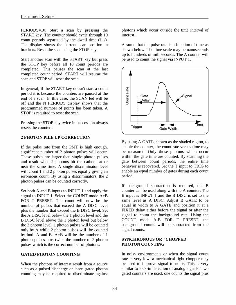
PERIODS=10. Start a scan by pressing the START key. The counter should cycle through 10 count periods separated by the dwell time (1 s). The display shows the current scan position in brackets. Reset the scan using the STOP key. Start another scan with the START key but press the STOP key before all 10 count periods are completed. This pauses the scan at the last completed count period. START will resume the scan and STOP will reset the scan. In general, if the START key doesn't start a count period it is because the counters are paused at the end of a scan. In this case, the SCAN led will be off and the N PERIODS display shows that the programmed number of points has been taken. A STOP is required to reset the scan. Pressing the STOP key twice in succession always resets the counters. 2 PHOTON PILE UP CORRECTION If the pulse rate from the PMT is high enough, significant number of 2 photon pulses will occur. These pulses are larger than single photon pulses and result when 2 photons hit the cathode at or near the same time. A single discriminator level will count 1 and 2 photon pulses equally giving an erroneous count. By using 2 discriminators, the 2 photon pulses can be counted correctly. Set both A and B inputs to INPUT 1 and apply the signal to INPUT 1. Select the COUNT mode A+B FOR T PRESET. The count will now be the number of pulses that exceed the A DISC level plus the number that exceed the B DISC level. Set the A DISC level below the 1 photon level and the B DISC level above the 1 photon level but below the 2 photon level. 1 photon pulses will be counted only by A while 2 photon pulses will be counted by both A and B. A+B will be the number of 1 photon pulses plus twice the number of 2 photon pulses which is the correct number of photons. GATED PHOTON COUNTING When the photons of interest result from a source such as a pulsed discharge or laser, gated photon counting may be required to discriminate against
photons which occur outside the time interval of interest. Assume that the pulse rate is a function of time as shown below. The time scale may be nanoseconds up to hundreds of milliseconds. The A counter will be used to count the signal via INPUT 1.
By using A GATE, shown as the shaded region, to enable the counter, the count rate versus time may be measured. Only those photons which occur within the gate time are counted. By scanning the gate between count periods, the entire time behavior is recovered. Set the T input to TRIG to enable an equal number of gates during each count period. If background subtraction is required, the B counter can be used along with the A counter. The B input is INPUT 1 and the B DISC is set to the same level as A DISC. Adjust B GATE to be equal in width to A GATE and position it at a FIXED delay either before the signal or after the signal to count the background rate. Using the COUNT mode A-B FOR T PRESET, the background counts will be subtracted from the signal counts. SYNCHRONOUS OR "CHOPPED" PHOTON COUNTING In noisy environments or when the signal count rate is very low, a mechanical light chopper may be used to improve signal to noise. This is very similar to lock-in detection of analog signals. Two gated counters are used, one counts the signal plus
Instrument Setups
35
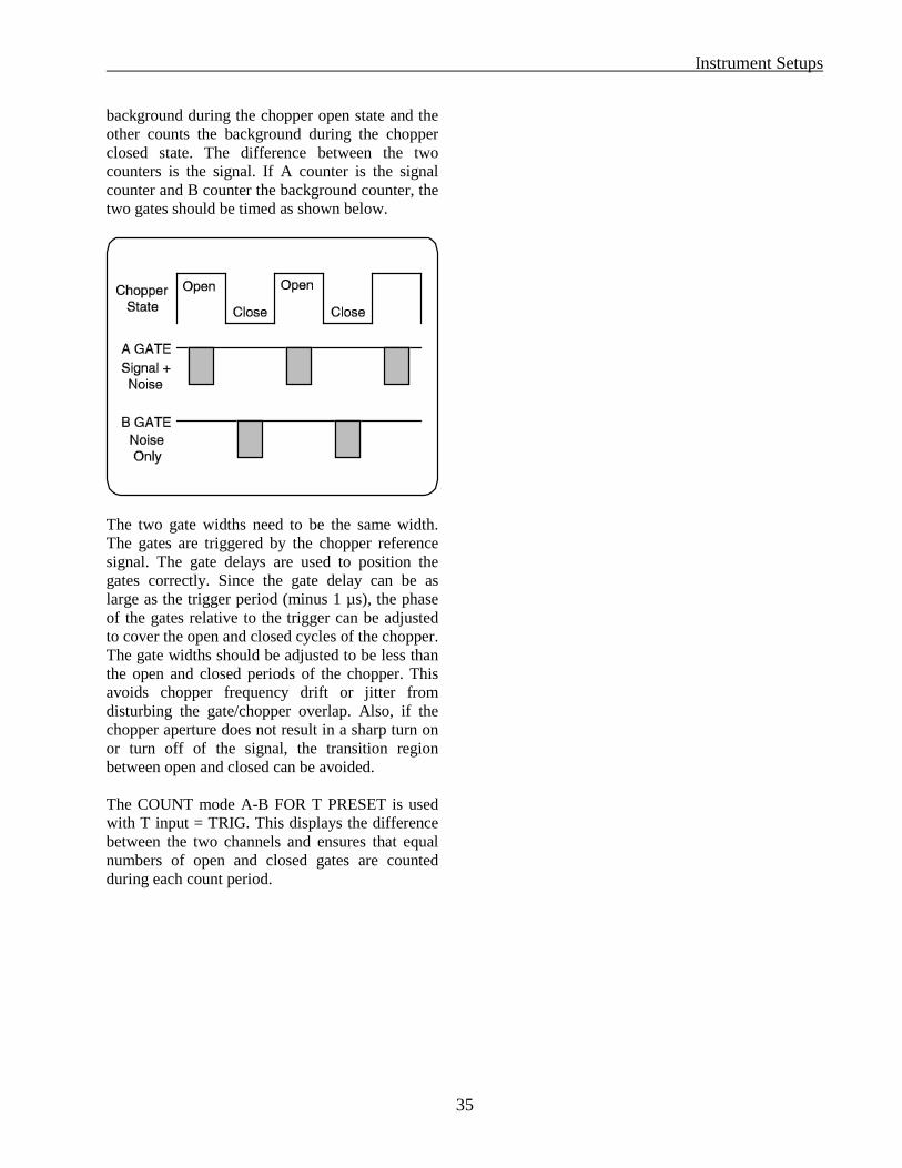
background during the chopper open state and the other counts the background during the chopper closed state. The difference between the two counters is the signal. If A counter is the signal counter and B counter the background counter, the two gates should be timed as shown below.
The two gate widths need to be the same width. The gates are triggered by the chopper reference signal. The gate delays are used to position the gates correctly. Since the gate delay can be as large as the trigger period (minus 1 µs), the phase of the gates relative to the trigger can be adjusted to cover the open and closed cycles of the chopper. The gate widths should be adjusted to be less than the open and closed periods of the chopper. This avoids chopper frequency drift or jitter from disturbing the gate/chopper overlap. Also, if the chopper aperture does not result in a sharp turn on or turn off of the signal, the transition region between open and closed can be avoided. The COUNT mode A-B FOR T PRESET is used with T input = TRIG. This displays the difference between the two channels and ensures that equal numbers of open and closed gates are counted during each count period.

Instrument Setups
36
Remote Programming
37
REMOTE PROGRAMMING The SR400 Photon Counter is remotely programmable via both RS-232 and GPIB (IEEE-488) interfaces. It may be used with laboratory computers or simply with a terminal. All front panel features (except power) may be controlled and read via the computer interfaces. The SR400 also has two programmable analog output ports available to provide general purpose control voltages. COMMUNICATING WITH THE SR400 Before using either the RS-232 or GPIB interface, the appropriate communication parameters need to be set. These parameters are set from the front panel in the COM menu. If the GPIB interface is being used, only the GPIB address of the instrument needs to be set. If the RS-232 interface is being used, the baud rate, number of bits in a character, and parity need to be set. The RS-232 wait interval programs the delay between characters sent from the SR400. The delay is the wait value times 3.3 ms. For most computers this can be set to 0. Some terminal emulators may require a delay. The RS-232 echo mode should be OFF if the SR400 is connected to a computer. It may ON if connected to a terminal. COMMAND SYNTAX Communications with the SR400 use ASCII characters. Commands to the SR400 may be in either UPPER or lower case. A command to the SR400 consists of two command letters, arguments or parameters if necessary, and an ASCII carriage return (<cr>) or line-feed (<lf>) or both. The different parts of the command do not need to be separated by spaces. Spaces can improve the readability of your programs and, if included in a command, they will be ignored. If more than one parameter is required by a command, the parameters must be separated by a comma. Examples of commands are: CM 1 <cr> set the counting mode to A-B
FOR T PRESET
CI 0,1 <cr> set the input to counter A to INPUT 1
NP 5E2 <cr> set N PERIODS to 500 GD 0,1.2E-6 <cr> set A gate delay to 1.2 µs PL 1, -3.4E-1<cr> set the PORT1 output to
-0.34 V Multiple commands may be sent on a single line. The commands must be separated by a semicolon (;) character. The commands will not be executed until the terminating carriage return is sent. An example of a multiple command is: CM 1; CI 0,1; GD 0,1.2E-6 <cr> It is not necessary to wait between commands. The SR400 has a command input buffer of 256 characters and processes the commands in the order received. Likewise, the SR400 has an output buffer (for each interface) of 256 characters. If a buffer overflows, the message "DATA BUFFER OVERFLOW" appears on the LCD display for 5 s and all buffered data is erased. In general, if a command is sent without parameters, it is interpreted as a request to read the value of the associated function or setting. Values returned by the SR400 are sent as a string of ASCII characters terminated usually by carriage return, line-feed. For example, after the above command is sent, the following read commands would generate the responses shown below. Command Response from SR400 CM1 <cr><lf> CI 0 1<cr><lf> GD 0 1.2E-6<cr><lf> The choice of terminating characters sent by the SR400 is determined by which interface is being used and whether the 'echo' feature is in use. The terminating sequence for the GPIB interface is always <cr><lf>. The default sequence for RS-232 is <cr> when the echo mode is off, and <cr><lf> when the echo mode is on. The terminating sequence for the RS-232 interface may be changed using the SE command.

Remote Programming
38
Note that the terminating characters are sent with each value returned by the SR400. Thus, the response to the command string CM;CI0;GD0<cr> while using the RS-232 non-echo mode would be 1<cr>1<cr>1.2E-6<cr>. In general, it is good programming practice to receive the response from one query command before sending another command. FRONT PANEL STATUS LED's The ACT LED flashes whenever the SR400 is sending or receiving characters over the computer interfaces. The ERR LED flashes whenever an error has occurred, such as, an illegal command has been received, a parameter is out of range, or a communication buffer has exceeded 240 characters. The REM LED is on whenever the SR400 is programmed to be in the remote (front panel locked out) state. RS-232 ECHO AND NO ECHO OPERATION In order to allow the SR400 to be operated from a terminal, an echo feature has been included which causes the unit to echo back commands received over the RS-232 port. This feature is enabled by setting the RS-232 ECHO mode to ON in the COM menu. In this mode, the SR400 will send line-feeds in addition to carriage returns with each value returned and will also send the prompts 'OK>' and '??>' to indicate that the previous command line was either processed correctly or contained an error. Operating the SR400 from a terminal is an ideal way to learn the commands and responses before attempting to program a computer to control the SR400. When the unit is controlled by a computer, the echo feature should be turned OFF to prevent the sending of spurious characters which the computer is not expecting. TRY-OUT WITH AN ASCII TERMINAL Before attempting any detailed programming with the SR400, it is a good idea to try out the commands using a terminal. Connect a terminal
with an RS-232 port to the RS-232 connector on the rear panel of the SR400. A 'straight' RS-232 cable is required since the SR400 is a DCE and the terminal is a DTE. After connecting the terminal, hold down the STOP key while turning the unit on. This causes the SR400 to assume its default settings so that the following discussion will agree with the actual responses of the SR400. Set the baud rate, parity, and character length to match the terminal using the COM menu. The RS-232 echo mode should be changed to ON. Now turn the unit off and on again. The ACT LED will flash for a second and the sign-on message will appear on the terminal. Following the message, the prompt 'OK>' will be displayed. This indicates that the SR400 is ready to accept commands. The sign on message is only sent if the RS-232 echo mode is ON. Type the letters 'CM' followed by a carriage return (CM<cr>). The SR400 responds by sending to the terminal the character 0 indicating that the counting mode is A,B FOR T PRESET. In general, a command with no arguments or parameters reads a setting of the unit. Now type the command MD1,2<cr>. The menu line of the display should now read A=INPUT 1. Type the command CI0,0<cr> to change the counter A input to 10 MHz. The menu line should now read A=10MHz. Now use the command CS<cr> to start counting. After one second, counter A should have 10000000 displayed (10 MHz for 1 second). The data from counter A can now be read. Type the command QA<cr> and the response should be the counter A value. Attach a dc voltmeter to the PORT1 D/A output on the rear panel. The range should allow for 10V readings. The voltage at this output can be set using the PL command. Type PL1,5.0<cr> and the output will change to 5.0V. To read this back to the terminal, just type PL1<cr>. When setting the voltage, the value may be sent as an integer (5), real (5.000), or floating point (0.500E1) number. At this point, the user should experiment with a few of the commands. A detailed command list follows.

Remote Programming – Command List
39
DETAILED COMMAND LIST The two letters in each command sequence specify the command. The rest of the sequence consists of parameters. Multiple parameters are separated by a comma. Those parameters shown in are optional while those without are required. Variable i is an integer which selects a counter: i Counter 0 A 1 B 2 T Variables i,j,k,l, and m are integers and must be expressed in integer format. Variable n is a real number >= 1 with one significant digit (i.e. 20 or 5E5). Variable x is a real number with one significant digit (i.e. 2E-3 or .002). Variables n,x,t, and v are real numbers in integer, real, or floating point format.
MODE CM j If j is included, the CM command sets the counting mode. If j is absent, the counting mode is returned. j Counting Mode 0 A,B FOR T PRESET 1 A-B FOR T PRESET 2 A+B FOR T PRESET 3 A FOR B PRESET Setting the counter mode also performs a counter reset. CI i ,j The CI command sets and reads the counter inputs. i = 0, 1, or 2 selecting counter A,B, or T and is required. If j is included, then the input to counter i is changed to source j. If j is absent, the input to counter i is returned.
j Input 0 10 MHz 1 INPUT 1 2 INPUT 2 3 TRIG Counter Allowed Inputs A 10 MHz, INPUT1 B INPUT 1, INPUT 2 T 10 MHz, INPUT 2, TRIG Changing a counter input while counting may result in bad count data. CP i ,n The CP command sets and reads the counter presets. If i = 1 then counter B is selected, if i = 2 counter T is selected. The parameter i is required. If n is included, then counter i is preset to n where n is a value from 1 to 9E11. n may be expressed in any format but must be greater than or equal to 1 and only the most significant digit is used. For example, "CP2,10" , "CP2,1E1" , "CP2,0.1E2" , "CP2,12" all set T SET to 1E1. Changing a counter preset while counting causes the counters to pause. A counter start command or keypress resumes counting. If n is absent, then the preset value of counter i is returned. In the above example, the string "1E1" is returned. Note that n is the number of cycles of the 10 MHz clock, not seconds. NP m If m is absent, the NP command returns the programmed number of periods in a scan (N PERIODS). If m is included, the number of periods is set to the value m. The parameter m must be an integer from 1 to 2000. Changing the number of periods during a scan is allowed. If the new value exceeds the current scan position, then the scan will continue to the new number of periods. If the new value is lower than the current scan position, then the scan ends at the next end of count period. NN The NN command reads the scan position. The scan position is the number of count periods or
Remote Programming – Command List
40
data points completed so far during the current scan and is shown in the brackets on the N PERIODS menu line. The NN command is a read only command. NE j If j = 0, the NE command sets the scan end mode (AT N) to STOP. If j = 1, the mode is set to START. The scan end mode may be changed at any time. If j is absent, the scan end mode is returned. DT x The DT command reads and sets the dwell time. If x is absent, the dwell time is returned. If x is included, the dwell time is set to x seconds where 2E-3 <= x <= 6E1. If x = 0, the dwell is set to EXTERNAL. Only the most significant digit of x is used so "DT 2E-3" , "DT .0022" , "DT 2.2E-3" all set the dwell to 2 ms. AS j The AS command reads and sets the front panel D/A output source. If j is absent, the D/A source is returned. The parameter j may only be included if the counting mode is A,B FOR T PRESET. In this case, j=0 or 1 selects A or B. In all other modes, the D/A output follows the count display. The source may be read in all modes. j Output source 0 A 1 B 2 A-B 3 A+B AM j If j is included, the AM command sets the D/A output scale. If j is absent, the D/A output scale is returned. j Output scale 0 Log (1V/decade) 1 987###### 2 #876##### 3 ##765#### 4 ###654### 5 ####543## 6 #####432# 7 ######321
SD j If j = 1, the SD command sets the count display mode to HOLD. If j = 0, the display mode will be CONTINUOUS. If j is absent, the display mode is returned.
LEVELS TS j If j = 1, the TS command sets the gate trigger slope to FALL or negative. If j = 0, the gate trigger slope is set to RISE or positive. If j is absent, the gate trigger slope is returned. TL v If v is absent, the TL command returns the gate trigger level. When v is included, the trigger level is set to v Volts where -2.000 <= v <= 2.000. The resolution is .001 V. DS i ,j The DS command sets and reads the discriminator slopes. i = 0,1, or 2 designates discriminator A,B, or T and is required. If j is included, the selected discriminator slope is set to RISE, j=0, or FALL, j=1. If j is absent, the slope of discriminator i is returned. DM i ,j The DM command sets and reads the discriminator modes. i = 0,1, or 2 designates discriminator A,B, or T and is required. If j is included, the selected discriminator is set to FIXED, j=0, or SCAN, j=1. If j is absent, the mode of discriminator i is returned. The mode may be changed during a scan. If it is changed to SCAN, the level begins scanning from the start value on the next count period. If it is changed to FIXED, the level returns to the start value immediately. DY i ,v The DY command sets and reads the discriminator scan step size. i = 0,1, or 2 designates discriminator A,B, or T and is required. If v is included, the selected discriminator scan step is set to v Volts where -0.0200 <= v <= 0.0200. The resolution is 0.0002 V (0.2 mV). If v is absent, the selected discriminator scan step is returned. The scan step may be set and read even if the selected
Remote Programming – Command List
41
discriminator is in the FIXED mode. Changing the scan step during a scan will affect the level for the next count period and all those that follow. DL i ,v The DL command sets and reads the discriminator levels. i = 0,1, or 2 designates discriminator A,B, or T and is required. If v is included, the selected discriminator level is set to v Volts where -0.3000 <= V <= 0.3000. The resolution is 0.0002 V (0.2 mV). If v is absent, the selected discriminator level is returned. If the discriminator mode is SCAN, the DL command sets and reads the starting value of the level. Changing the level during a scan will cause the level to be set to the new value on the next count period. Note that the scan is not reset. Reading the level during a scan always returns the starting value, not the current value. DZ i The DZ command returns the level of discriminator i during a scan. i = 0,1, or 2 designates discriminator A,B, or T and is required. If discriminator i is in the SCAN mode, its current level during a scan is read. If the counters are in reset or the discriminator is in the FIXED mode, the DZ command returns the starting value for the level (same as DL command). The DZ command is a read only command. PM i ,j The PM command sets and reads the rear panel PORT1 and PORT2 D/A output modes. i=1 or 2 to select PORT1 or PORT 2 and is required. If j is included, the mode is set to FIXED, j=0, or SCAN, j=1. If j is absent, the mode is returned. The mode may be changed during a scan. If it is changed to SCAN, the level begins scanning from the start value on the next count period. If it is changed to FIXED, the level returns to the start value immediately. PY i ,v The PY command sets and reads the PORT1 and PORT2 scan steps. i=1 or 2 to select PORT1 or PORT 2 and is required. If v is included, the scan step is set to v Volts where -0.500 <= v <= 0.500. The resolution is 0.005 V (5 mV). If v is absent, the scan step is returned. The scan step may be set and read even if the selected port is in the FIXED mode. Changing the scan step during a scan will
affect the level for the next count period and all those that follow. PL i ,v The PL command sets and reads thePORT1 and PORT2 output levels. i=1 or 2 to select PORT1 or PORT 2 and is required. If v is included, the output level is set to v Volts where -10.000 <= v <= 10.000. The resolution is 0.005 V (5 mV). If v is absent, the output level is returned. If the Port output mode is SCAN, the PL command sets and reads the starting value of the level. Changing the level during a scan will cause the level to be set to the new value on the next count period. Note that the scan is not reset. Reading the level during a scan always returns the starting value, not the current value. PZ i The PZ command returns the level of the PORT1 and PORT2 outputs during a scan. i=1 or 2 to select PORT1 or PORT 2 and is required. If the selected port is in the SCAN mode, its current level during a scan is read. If the counters are in reset or the output is in the FIXED mode, the PZ command returns the starting value for the level (same as PL command). The PZ command is a read only command.
GATES GM i ,j The GM command sets and reads the gate modes. i = 0 or 1 designates A gate or B gate and is required. If j is included, the selected gate is set to CW, j=0, or FIXED, j=1, or SCAN, j=2. If j is absent, the mode of gate i is returned. The mode may be changed during a scan. If it is changed to SCAN, the delay begins scanning from the start position on the next count period. If it is changed to FIXED, the delay returns to the start position immediately. If it is changed to CW, the gate immediately changes to continuously on. GY i ,t The GY command sets and reads the gate delay scan step. i = 0 or 1 designates A gate or B gate and is required. If t is included, the selected gate scan step is set to t seconds where 0 <= t <=
Remote Programming – Command List
42
99.92E-3. The resolution is variable depending upon the 4 most significant digits of t. 4 most significant digits resolution in 4th digit 1000 to 2048 1 (1001,1002,1003,...) 2048 to 4096 2 4096 to 8192 4 8192 to 9992 8 (8192,8200,8208,...) For example, near 10.00 µs, the allowed values of t are 9.984 µs, 9.992 µs, 10.00 µs, 10.01 µs, etc. Below 1.000 µs, the resolution is 1 ns. Almost any value of t may be sent and the SR400 will round to the nearest allowed value. If t is absent, the selected gate scan step is returned. The scan step may be set and read even if the selected gate is not in the SCAN mode. Changing the scan step during a scan will affect the gate position for the next count period and all those that follow. GD i ,t The GD command sets and reads the gate delays. i=0 or 1 designates A gate or B gate and is required. If t is included, the selected gate delay is set to t seconds where 0 <= t <= 999.2E-3. The resolution is variable depending upon the 4 most significant digits of t. 4 most significant digits resolution in 4th digit 1000 to 2048 1 (1001,1002,1003,...) 2048 to 4096 2 4096 to 8192 4 8192 to 9992 8 (8192,8200,8208,...) For example, near 10.00 µs, the allowed values of t are 9.984 µs, 9.992 µs, 10.00 µs, 10.01 µs, etc. Below 1.000 µs, the resolution is 1 ns. Almost any value of t may be sent and the SR400 will round to the nearest allowed value. If t is absent, the selected gate delay is returned. The gate delay may be set and read regardless of the gate mode. If the mode is CW, the gate remains continuous. If the mode is SCAN, the GD command sets and reads the starting position of the gate delay. Changing the delay during a scan will cause the delay to be set to the new value on the next count period. Note that the scan is not reset. Reading the delay during a scan always returns the starting delay, not the current delay.
GZ i The GZ command returns the gate delay position during a scan. i = 0 or 1 designates A gate or B gate and is required. If gate i is in the SCAN mode, its current delay position during a scan is read. If the counters are in reset or the gate is not in the SCAN mode, the GZ command returns the starting delay position (same as GD command). The GZ command is a read only command. GW i ,t The GW command sets and reads the gate widths. i = 0 or 1 designates A gate or B gate and is required. If t is included, the selected gate width is set to t seconds where 0.005E-6 <= t <= 999.2E-3. The resolution is variable depending upon the 4 most significant digits of t. 4 most significant digits resolution in 4th digit 1000 to 2048 1 (1001,1002,1003,...) 2048 to 4096 2 4096 to 8192 4 8192 to 9992 8 (8192,8200,8208,...) For example, near 10.00 µs, the allowed values of t are 9.984 µs, 9.992 µs, 10.00 µs, 10.01 µs, etc. Below 1.000 µs, the resolution is 1 ns. Almost any value of t may be sent and the SR400 will round to the nearest allowed value. If t is absent, the selected gate width is returned. The gate width may be read and set regardless of the gate mode. If the mode is CW, the gate remains continuous. If the mode is FIXED or SCAN, the gate width is adjusted immediately. NOTE Changing the gate delay or width may cause some gates to be missed or shortened. Changing gate parameters while counting may therefore cause bad data to be collected. It is recommended that the counters be paused before changing gate values and then started again.
FRONT PANEL CS Sending the CS command has the same effect as pressing the START key. The CS command may be sent at any time but only has an effect if the counters are paused or in reset. If the DWELL
Remote Programming – Command List
43
TIME is EXTERNAL, the CS command will start a count period. A CH command may be sent to terminate the count period. CH Sending the CH command has the same effect as pressing the STOP key. The CH command may be sent at any time. If recieved while scanning, the scan will pause. If received while paused, the counters will reset. If the DWELL TIME is EXTERNAL, the CH command may be used to terminate count periods. CR Sending the CR command resets the counters. All scanning parameters return to their start values and previously buffered scan data is lost. The CR command has the same effect as pressing the STOP key twice in succession. CK j The CK command simulates pressing a front panel key. j is a required parameter from 0 to 13. The CK command may be sent at any time and is not restricted by the remote/local state of the front panel. j key 0 DOWN CURSOR 1 RIGHT CURSOR 2 LEVEL 3 SETUP 4 COM 5 STOP 6 LOCAL 7 RESET 8 LEFT CURSOR 9 UP CURSOR 10 MODE 11 AGATE 12 BGATE 13 START SC The SC command reads the cursor position. "0" is returned for left, "1" for right, and "2" for inactive. To move the cursor, use the CK command. MI j The MI command sets the front panel inhibit mode. j is a required parameter from 0 to 2.
j Mode 0 Local: all front panel controls are
operative 1 Remote: front panel controls are not
operative. The LOCAL (COM) key returns the status to local.
2 Lock-out: front panel controls are not operative. No key returns the status to local. Another MI command is needed to return to local.
The MI command may only be sent via the RS-232 interface. The GPIB interface uses REN, LLO, and GTL to set the front panel mode. MS string The MS command writes user messages on the menu line of the LCD display. String may be up to 24 characters long with spaces represented by underscores. For example, the command "MS HELLO_THERE" puts the message "HELLO THERE" on the display. The display will return to normal when any active key is pressed. It will also return to normal if the current menu line needs to be updated during a scan. The MS command without a string returns the display to normal immediately. MD j,k The MD command changes the menu display to line k of menu j. The allowed combinations of j and k are shown below. Both j and k are required parameters. j,k 1,1 COUNT 1,2 A 1,3 B 1,4 T 1,5 N PERIODS 1,6 AT N 1,7 D/A OUT 1,8 D/A RANGE 1,9 DISPLAY 2,1 A GATE 2,2 A DELAY 2,3 A WIDTH 3,1 B GATE

Remote Programming – Command List
44
j,k 3,2 B DELAY 3,3 B WIDTH 4,1 TRIG SLOPE 4,2 TRIG LVL 4,3 A DISC SLOPE 4,4 A DISC MODE 4,5 A DISC LVL 4,6 B DISC SLOPE 4,7 B DISC MODE 4,8 B DISC LVL 4,9 T DISC SLOPE 4,10 T DISC MODE 4,11 T DISC LVL 4,12 PORT1 MODE 4,13 PORT1 LVL 4,14 PORT2 MODE 4,15 PORT2 LVL 5,1 GPIB ADDR 5,2 RS-232 BAUD 5,3 RS-232 BITS 5,4 RS-232 PARITY 5,5 RS-232 WAIT 5,6 RS-232 ECHO 5,7 DATA 6,1 LCD CONTRAST 6,2 STORE 6,3 RECALL MM The MM command reads the menu number of the display (j in the above table). The MM command is a read only command. ML The ML command reads the menu line of the display (k in the above table). The ML command is a read only command.
INTERFACE CL The CL command resets the unit to its default state. The default front panel settings are listed in the Instrument Setups section. Parameters in the SETUP and COM menus are not changed. In addition, the SRQ mask is cleared, and the RS-232
terminating sequence is reset to the proper defaults. The command and output buffers are cleared by the CL command. Therefore, it is bad practice to use the CL command before all previous commands have been processed and all responses have been received. There should never be any other commands on the same line as a CL command. SS j The SS command reads the status byte. (See the following section for a definition of the status byte). j designates one bit, 0-7, of the status byte. If j is included, the designated bit of the status byte is returned ("0" or "1"). The bit which is read is then reset. If j is absent, the value of the entire byte is returned (0-255) and all status bits are then reset. SI j The SI command reads the secondary status byte. (See the following section for a definition of the secondary status byte). j designates one bit, 0-2, of the byte. If j is included, the designated bit of the secondary status byte is returned ("0" or "1"). The bit which is read is then reset. If j is absent, the value of the entire byte is returned (0-7) and all secondary status bits are then reset. SV m If m is included, the SV command sets the GPIB SRQ (service request) mask to the value m (0-255). If m is absent, the value of the SRQ mask is returned. The SV command may only be sent via the GPIB interface. SW m The SW command sets and reads the RS-232 character wait interval. If m is included, the SR400 will wait m times 3.3 ms between characters sent over the RS-232 interface. This allows slow computer interfaces to keep up. m can range from 0 to 25. If m is absent, the wait value is returned. The SW command may only be sent via the RS-232 interface. SE j,k,l,m The SE command sets the RS-232 end-of-record characters sent by the SR400 to those specified by

Remote Programming – Command List
45
the decimal ASCII codes (0-127) j,k,l, and m. If no argument is included, the end-of-record sequence returns to the default (a carriage return), otherwise, up to four characters may be specified. The end-of-record required by the SR400 when receiving commands is not affected. The SE command may only be sent via the RS-232 interface.
STORE/RECALL ST m The ST command stores the instrument settings to location m = 1 to 9. Parameters in the SETUP and COM menus are NOT stored by this command. The SETUP and COM parameters are stored on power down as part of the current setup. RC m The RC command recalls instrument settings from location m = 0 to 9. If m = 0, the default settings are recalled (see the Instrument Setups section for a list of the default settings). In all cases, the SETUP and COM parameters are not altered by this command. The RC command also resets the counters. The menu display returns to the menu displayed when the instrument settings were stored. This is very often the STORE menu.
POLLED DATA QA QB The QA command reads the most recent complete data point from counter A, QB reads the most recent data point from counter B. QA and QB commands should only be sent after checking the Data Ready status bit. This bit is set at the end of each complete count period and signals the availability of valid data. The Data Ready status bit is reset after it is read. Sending QA or QB commands without polling the Data Ready status can cause data points to be read multiple times. Note that QA and QB do not reset the Data Ready status. If data is not ready, the QA and QB commands return -1. If counter B is preset, QB returns -1. QA m
QB m When m is included in a QA or QB command, buffered data from scan point m is read. m = 1 is the first data point in the scan and m = N PERIODS is the last data point. If m>2000 or m=0, an error occurs. If counter B is preset, then QB m returns 1. If m > last completed point of the current scan, then -1 is returned. Therefore during a scan, QA 1 can be sent until a positive count is returned. At this point, the QA 2 command should be sent until a positive count is returned. All data from the scan can be read in this manner. This is the fastest way to read data during a scan while still maintaining full handshaking. Data from the scan buffer can also be read after the scan is completed. The Scan Done status bit can be polled to determine when the scan finishes. The Scan Done status bit is set at the end of a scan only if the scan end mode is STOP. The Scan Done status bit is reset after it is read. To prevent ambiguity, the status byte should be cleared before starting a scan and then polled to determine when the scan is finished. Whenever scan data is to be read, the scan end mode should be STOP and a new scan started only after reading the desired data from the previous scan. If m is absent or between 1 and 2000, data is always returned from a Q command. The value -1 is reserved for errors.
CONTINUOUS DATA EA EB ET The E commands dump the scan buffers at the end of a scan. The E commands may only be sent while paused at the end of a scan. Data will be sent continuously starting with data point 1 and ending with data point N PERIODS. Each data point is separated by an end-of-record sequence. If an E command is used with the RS-232 interface, the controlling computer interface should be interrupt driven or have fast data communication routines
Remote Programming – Command List
46
since the data transmission is limited only by the baud rate and the character wait interval. The EA command dumps the counter A buffer, EB dumps the counter B buffer, and ET dumps both counters. EB and ET generate errors if counter B is preset. Data from the ET command is ordered A1,B1,A2,B2,... with each data point separated by the terminator sequence. FA FB FT The F commands start a new scan. Data is returned at the end of each count period. Data continues to be returned until all N PERIODS points are completed and sent. If data points accumulate faster than they can be sent over the computer interface, they are buffered and sent as fast as the interface allows. F commands may only be sent when the counters are in reset. The FA command starts the scan and returns the next N PERIODS data points from counter A. FB returns points from counter B and FT returns points from both counters. FB and FT generate errors if counter B is preset. Data from the FT command is ordered A1,B1,A2,B2,... with each data point separated by the terminator sequence. NOTE Scan buffers are reset at the start of each scan. When the counters reset, data from the previous scan is lost and any actively transmitting E or F command is terminated. Thus, programs may hang if the counters are reset or a new scan is started before all data points from the previous scan are received. To prevent this, the scan end mode should be STOP and a new scan initiated only after receiving N PERIODS data points. An E command sent while a previous E command is still executing generates an error.
EXAMINE DATA XA XB The X commands read the counter contents regardless of the count state. An X command sent
while counting returns the current counter contents. If the counters are in the dwell cycle, paused, or reset, the counter value will be zero. The display may still be showing the most recently completed count but the counters are already internally reset. The X command is generally only useful for long count periods and/or slow count rates. If the count rate is faster than the interface speed, then the returned count values may be in error. The XA command reads the contents of counter A. XB reads the contents of counter B. XB returns -1 if counter B is preset.
STATUS BYTE The SR400 maintains an 8-bit status register which the user may read to obtain information on the unit's status. The status byte is read using the SS command which returns the value of the byte in ASCII coded decimal. The returned status byte reflects all of the status conditions which have occurred since the last time the byte was read. After the status byte has been read, it is cleared. Thus, the status byte should be read initially to clear all previous conditions (especially after a power up or after settings have been changed). The definitions for each bit of the status byte are given below: Bit 0 Parameter Changed from front panel. When this bit is set, it indicates that the front panel knob has been rotated and a setting has been altered. Bit 1 Data Ready. This bit is set at the end of each count period to indicate that counter data is available. Bit 2 Scan Finished. This bit is set at the end of a scan if the scan end mode is STOP to indicate that the scan buffer is available for reading. This bit is not set if the scan end mode is START. Bit 3 Counter Overrun. This bit is set whenever counter A or B exceeds or equals109-1 counts.
Remote Programming – Command List
47
Bit 4 Rate Error. This bit is set whenever a gate is missed. This can occur if a gate delay or width exceeds the trigger period minus 1 µs. Bit 5 Recall Error. This bit is set if a recall from a stored setting detects an error in the recalled data. If an error is found, the instrument setup is not altered. Bit 6 SRQ. This bit is always zero when polled via the SS command. This bit is set in the status byte which is read via the GPIB serial poll following a service request generated by the SR400. Bit 7 Command Error. This bit is set when an illegal command is received.
SECONDARY STATUS BYTE The secondary status byte is actually only a 3 bit register. The secondary status byte is read using the SI command and returns a value from 0 to 7 in ASCII. The secondary status byte operates the same as the status byte above except that it cannot generate service requests. The definitions for each bit of the status byte are given below: Bit 0 Triggered. This bit is set when the gate generator is triggered. Bit 1 Inhibited. This bit is set when the discriminators are inhibited. Bit 2 Counting. This bit samples the state of the counters. If counting is in progress when this bit is polled, a 1 is returned, otherwise a 0 is returned. ERRORS/DATA WINDOW Whenever a parameter out of range or an unrecognized command error occurs, bit 7 of the status byte is set and the ERR LED flashes. In
addition, any commands remaining on the current command line (up to the next <cr>) are lost. To aid in determining the cause of the error, the last 254 characters received by the SR400 may be viewed on the LCD display using the DATA line of the COM menu. The knob may be used to scroll through the command buffer. The display always returns to the most recent data whenever the menu line is brought up or a new character is received. Any command that clears the communication buffers also clears this display window. This includes changing any COM parameters, resetting the instrument, or a buffer overflow. TROUBLE-SHOOTING INTERFACE PROBLEMS If you are having difficulty getting your computer to communicate with the SR400 look to the following sections on the RS-232 and GPIB interfaces for some tips specific to your particular interface. An ASCII terminal is a valuable aid for debugging interface problems. You can use it to: 1) become familiar with the SR400's command structure 2) substitute a human for the SR400 by using a null modem cable ( to make the DTE a DCE ) and attaching the terminal to the port to which you would normally have connected the SR400. This allows you to test your program's responses to inputs which you provide from the terminal. COMMON HARDWARE PROBLEMS INCLUDE: 1) The RS-232 or GPIB cables are not properly attached. 2) The COM parameters are incorrect for the RS-232 interface or the GPIB address is not set correctly (Make sure the RS-232 echo is off when using the RS-232 interface with a computer.) 3) Your computer requires an RS-232 control line to be asserted, but your cable does not pass it between the SR400 and the computer, or, your
Remote Programming – Command List
48
computer is not asserting the DTR line on the RS-232. COMMON SOFTWARE PROBLEMS INCLUDE: 1) You have sent the wrong command to ask for data from the SR400. Your program will wait forever for a response which is not going to come. This may not be your fault; we have seen Microsoft's Interpreted Basic on the IBM PC occasionally send a curly bracket (ASCII 253) when it was supposed to have sent a carriage return (ASCII 13). 2) Your computer's baud rate has been changed and no longer matches the SR400's baud rate. 3) The initial command sent to the SR400 was invalid due to a garbage character received during power-up, or, the first character in your computer's UART is garbage, also due to power-up. It is good practice to send a few carriage returns to the SR400 when your program begins, and have your program clear-out the UART at the start of your program. 4) The SR400 is not sending the correct 'end-of-record' marker for your computer. For example, it appears that Microsoft's Rev 3.2 FORTRAN on the IBM PC under DOS 2.1 requires two carriage returns for an end-of-record marker. The SE command can be used to set the SR400 end-of-record marker to 2 carriage returns. [The end-of-record marker is that sequence which indicates that the response is complete. From the keyboard, a single carriage return is the end-of-record marker.] 5) Answers are coming back from the SR400 too fast, overwriting the end-of-record markers, and causing the computer to hang, waiting for a complete response. In this case, the SW command can be used to slow down the response time of the SR400 preventing overwriting. 6) Answers are coming back from the SR400 too slowly due to the RS-232 wait interval being too large. Use the SW0 command at the beginning of your program to speed up the transmission from the SR400.
SR400 with the RS-232 Interface
49
SR400 WITH THE RS-232 INTERFACE The RS-232 is a popular serial interface standard for bit serial communication. Despite the existence of the standard there are many permutations of control lines, baud rates, and data formats. DATA COMMUNICATIONS EQUIPMENT (DCE) The SR400 is configured as DCE so that it may be connected directly to a terminal or IBM PC. If the SR400 is to be interfaced with another DCE device, a special cable (sometimes referred to as a 'null modem' cable) is required. To use the RS-232 interface you must set the COM parameters to match your computer's baud rate, parity, and number of bits. RS-232 ECHO The RS-232 ECHO should be OFF whenever the SR400 is interfaced with a computer. This prevents unwanted characters from being sent back to the computer after every command. The echo should be ON only if a terminal (or terminal emulator program) is being used. WAIT COMMAND The SR400 normally waits until the RS-232 'Clear to Send' control line (CTS) is asserted before sending characters. However, some computers do not set and reset the CTS line, possibly causing the SR400 to send data when the computer is not ready to read it. The SR400 may be 'slowed down' using the SW command. Sending 'SWn' causes the unit to wait nx3.3 ms before sending each character over the RS-232 interface. The command SW0 sets the wait interval to zero and results in the fastest transmission. The wait interval is set to 6 (20 ms) on power-up reset (STOP key held on power on). TERMINATION SEQUENCES The default RS-232 termination characters are sufficient to interface with most computers, however, it will occasionally be necessary to send
special terminating sequences to fit the requirements of some computers. This can be done with the SE command. The format for the command is: SE n1,n2,n3,n4 where n1, n2, n3, and n4 are decimal values between 0 and 255 corresponding to the ASCII codes of the desired termination characters. For instance, if the desired termination sequence is an asterisk, (ASCII 42), two carriage returns, (ASCII 13), and a line-feed, (ASCII 10), the appropriate command is: SE 42,13,13,10 If an NP command is sent requiring an answer of 100 (N PERIODS = 100), the SR400 would respond with the string 100*<cr><cr><lf> Up to four terminating characters may be specified by the SE command. If no arguments are sent with the SE command, the terminating sequence returns to the default (echo on: <cr><lf>; echo off: <cr>). The SE command does not affect the terminating character (<cr>) required at the end of commands received by the SR400. It also does not affect the terminating sequence sent with data over the GPIB interface. EXAMPLE PROGRAMS The following section lists several example programs which use the RS-232 port to control the SR400. All of the programs do the same thing, only the language is different. The programs set up the SR400 to count 10 MHz on counter A for 1 second. The counter data is read and the PORT1 output is ramped.
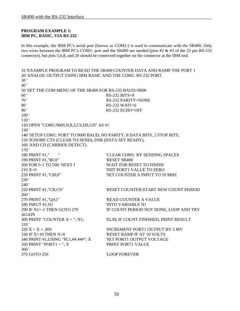
SR400 with the RS-232 Interface
50
PROGRAM EXAMPLE 1: IBM PC, BASIC, VIA RS-232 In this example, the IBM PC's serial port (known as COM1:) is used to communicate with the SR400. Only two wires between the IBM PC's COM1: port and the SR400 are needed (pins #2 & #3 of the 25 pin RS-232 connector), but pins 5,6,8, and 20 should be connected together on the connector at the IBM end. 10 'EXAMPLE PROGRAM TO READ THE SR400 COUNTER DATA AND RAMP THE PORT 1 20 'ANALOG OUTPUT USING IBM BASIC AND THE COM1: RS-232 PORT. 30 ' 40 ' 50 'SET THE COM MENU OF THE SR400 FOR RS-232 BAUD=9600 60 ' RS-232 BITS=8 70 ' RS-232 PARITY=NONE 80 ' RS-232 WAIT=6 90 ' RS-232 ECHO=OFF 100 ' 110 ' 120 OPEN "COM1:9600,N,8,2,CS,DS,CD" AS #1 130 ' 140 'SETUP COM1: PORT TO 9600 BAUD, NO PARITY, 8 DATA BITS, 2 STOP BITS, 150 'IGNORE CTS (CLEAR TO SEND), DSR (DATA SET READY), 160 'AND CD (CARRIER DETECT). 170 ' 180 PRINT #1," " 'CLEAR COM1: BY SENDING SPACES 190 PRINT #1,"RC0" 'RESET SR400 200 FOR I=1 TO 500: NEXT I 'WAIT FOR RESET TO FINISH 210 X=0 'INIT PORT1 VALUE TO ZERO 220 PRINT #1,"CI0,0" 'SET COUNTER A INPUT TO 10 MHZ 230 ' 240 ' 250 PRINT #1,"CR;CS" 'RESET COUNTER;START NEW COUNT PERIOD 260 ' 270 PRINT #1,"QA1" 'READ COUNTER A VALUE 280 INPUT #1,N1 'INTO VARIABLE N1 290 IF N1=-1 THEN GOTO 270 'IF COUNT PERIOD NOT DONE, LOOP AND TRY AGAIN 300 PRINT "COUNTER A = "; N1; 'ELSE IF COUNT FINISHED, PRINT RESULT 310 ' 320 X = X + .005 'INCREMENT PORT1 OUTPUT BY 5 MV 330 IF X>10 THEN X=0 'RESET RAMP IF AT 10 VOLTS 340 PRINT #1,USING "PL1,##.###"; X 'SET PORT1 OUTPUT VOLTAGE 350 PRINT "PORT1 = "; X 'PRINT PORT1 VALUE 360 ' 370 GOTO 250 'LOOP FOREVER
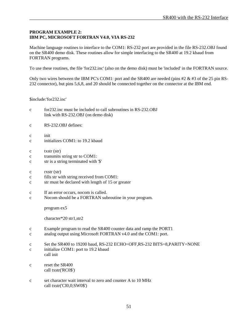
SR400 with the RS-232 Interface
51
PROGRAM EXAMPLE 2: IBM PC, MICROSOFT FORTRAN V4.0, VIA RS-232 Machine language routines to interface to the COM1: RS-232 port are provided in the file RS-232.OBJ found on the SR400 demo disk. These routines allow for simple interfacing to the SR400 at 19.2 kbaud from FORTRAN programs. To use these routines, the file 'for232.inc' (also on the demo disk) must be 'included' in the FORTRAN source. Only two wires between the IBM PC's COM1: port and the SR400 are needed (pins #2 & #3 of the 25 pin RS-232 connector), but pins 5,6,8, and 20 should be connected together on the connector at the IBM end. $include:'for232.inc' c for232.inc must be included to call subroutines in RS-232.OBJ
link with RS-232.OBJ (on demo disk) c RS-232.OBJ defines: c init c initializes COM1: to 19.2 kbaud c txstr (str) c transmits string str to COM1: c str is a string terminated with '$' c rxstr (str) c fills str with string received from COM1: c str must be declared with length of 15 or greater c If an error occurs, nocom is called. c Nocom should be a FORTRAN subroutine in your program. program ex5 character*20 str1,str2 c Example program to read the SR400 counter data and ramp the PORT1 c analog output using Microsoft FORTRAN v4.0 and the COM1: port. c Set the SR400 to 19200 baud, RS-232 ECHO=OFF,RS-232 BITS=8,PARITY=NONE c initialize COM1: port to 19.2 kbaud call init c reset the SR400 call txstr('RC0$') c set character wait interval to zero and counter A to 10 MHz call txstr('CI0,0;SW0$')
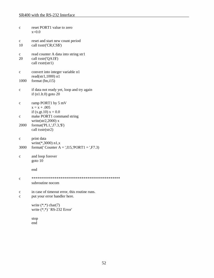
SR400 with the RS-232 Interface
52
c reset PORT1 value to zero x=0.0 c reset and start new count period 10 call txstr('CR;CS$') c read counter A data into string str1 20 call txstr('QA1$') call rxstr(str1) c convert into integer variable n1 read(str1,1000) n1 1000 format (bn,i15) c if data not ready yet, loop and try again if (n1.lt.0) goto 20 c ramp PORT1 by 5 mV x = x + .005 if (x.gt.10) x = 0.0 c make PORT1 command string write(str2,2000) x 2000 format('PL1,',f7.3,'$') call txstr(str2) c print data write(*,3000) n1,x 3000 format(' Counter A = ',I15,'PORT1 = ',F7.3) c and loop forever goto 10 end c ********************************************** subroutine nocom c in case of timeout error, this routine runs. c put your error handler here. write (*,*) char(7) write (*,*) ' RS-232 Error' stop end
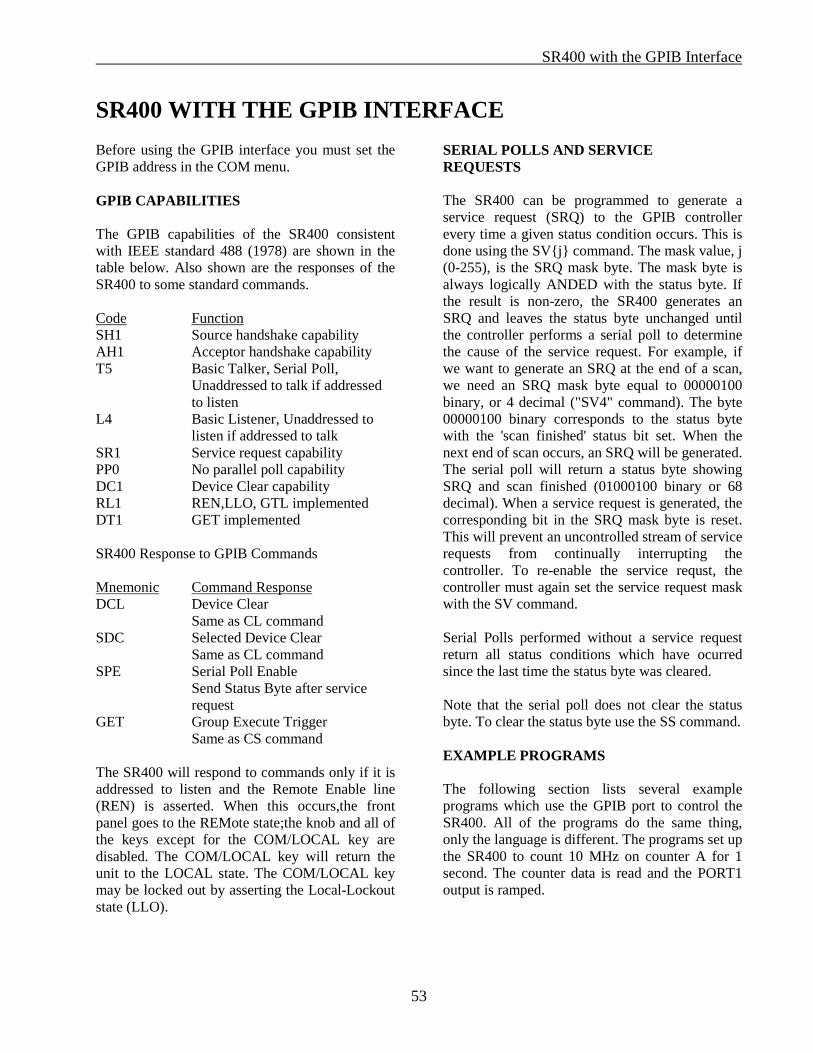
SR400 with the GPIB Interface
53
SR400 WITH THE GPIB INTERFACE Before using the GPIB interface you must set the GPIB address in the COM menu. GPIB CAPABILITIES The GPIB capabilities of the SR400 consistent with IEEE standard 488 (1978) are shown in the table below. Also shown are the responses of the SR400 to some standard commands. Code Function SH1 Source handshake capability AH1 Acceptor handshake capability T5 Basic Talker, Serial Poll,
Unaddressed to talk if addressed to listen
L4 Basic Listener, Unaddressed to listen if addressed to talk
SR1 Service request capability PP0 No parallel poll capability DC1 Device Clear capability RL1 REN,LLO, GTL implemented DT1 GET implemented SR400 Response to GPIB Commands Mnemonic Command Response DCL Device Clear Same as CL command SDC Selected Device Clear Same as CL command SPE Serial Poll Enable Send Status Byte after service
request GET Group Execute Trigger Same as CS command The SR400 will respond to commands only if it is addressed to listen and the Remote Enable line (REN) is asserted. When this occurs,the front panel goes to the REMote state;the knob and all of the keys except for the COM/LOCAL key are disabled. The COM/LOCAL key will return the unit to the LOCAL state. The COM/LOCAL key may be locked out by asserting the Local-Lockout state (LLO).
SERIAL POLLS AND SERVICE REQUESTS The SR400 can be programmed to generate a service request (SRQ) to the GPIB controller every time a given status condition occurs. This is done using the SVj command. The mask value, j (0-255), is the SRQ mask byte. The mask byte is always logically ANDED with the status byte. If the result is non-zero, the SR400 generates an SRQ and leaves the status byte unchanged until the controller performs a serial poll to determine the cause of the service request. For example, if we want to generate an SRQ at the end of a scan, we need an SRQ mask byte equal to 00000100 binary, or 4 decimal ("SV4" command). The byte 00000100 binary corresponds to the status byte with the 'scan finished' status bit set. When the next end of scan occurs, an SRQ will be generated. The serial poll will return a status byte showing SRQ and scan finished (01000100 binary or 68 decimal). When a service request is generated, the corresponding bit in the SRQ mask byte is reset. This will prevent an uncontrolled stream of service requests from continually interrupting the controller. To re-enable the service requst, the controller must again set the service request mask with the SV command. Serial Polls performed without a service request return all status conditions which have ocurred since the last time the status byte was cleared. Note that the serial poll does not clear the status byte. To clear the status byte use the SS command. EXAMPLE PROGRAMS The following section lists several example programs which use the GPIB port to control the SR400. All of the programs do the same thing, only the language is different. The programs set up the SR400 to count 10 MHz on counter A for 1 second. The counter data is read and the PORT1 output is ramped.
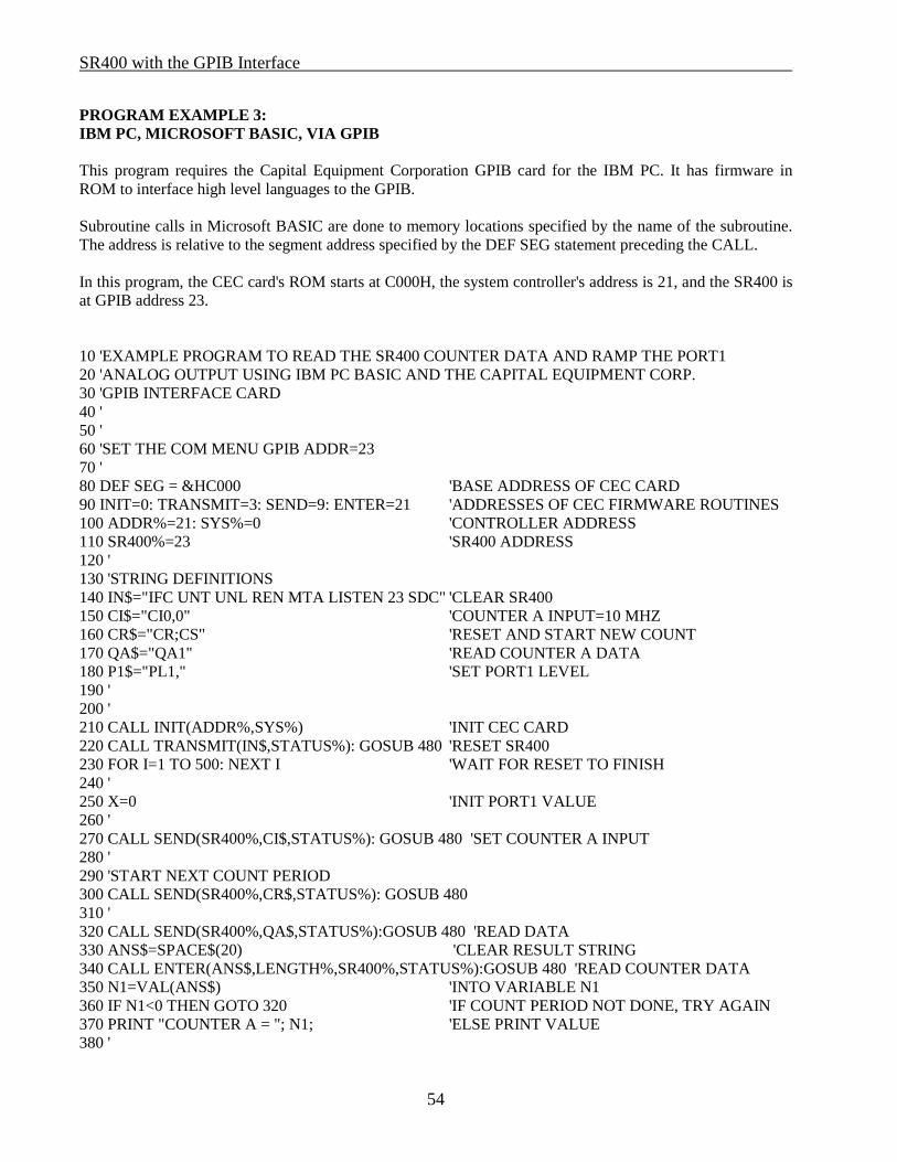
SR400 with the GPIB Interface
54
PROGRAM EXAMPLE 3: IBM PC, MICROSOFT BASIC, VIA GPIB This program requires the Capital Equipment Corporation GPIB card for the IBM PC. It has firmware in ROM to interface high level languages to the GPIB. Subroutine calls in Microsoft BASIC are done to memory locations specified by the name of the subroutine. The address is relative to the segment address specified by the DEF SEG statement preceding the CALL. In this program, the CEC card's ROM starts at C000H, the system controller's address is 21, and the SR400 is at GPIB address 23. 10 'EXAMPLE PROGRAM TO READ THE SR400 COUNTER DATA AND RAMP THE PORT1 20 'ANALOG OUTPUT USING IBM PC BASIC AND THE CAPITAL EQUIPMENT CORP. 30 'GPIB INTERFACE CARD 40 ' 50 ' 60 'SET THE COM MENU GPIB ADDR=23 70 ' 80 DEF SEG = &HC000 'BASE ADDRESS OF CEC CARD 90 INIT=0: TRANSMIT=3: SEND=9: ENTER=21 'ADDRESSES OF CEC FIRMWARE ROUTINES 100 ADDR%=21: SYS%=0 'CONTROLLER ADDRESS 110 SR400%=23 'SR400 ADDRESS 120 ' 130 'STRING DEFINITIONS 140 IN$="IFC UNT UNL REN MTA LISTEN 23 SDC" 'CLEAR SR400 150 CI$="CI0,0" 'COUNTER A INPUT=10 MHZ 160 CR$="CR;CS" 'RESET AND START NEW COUNT 170 QA$="QA1" 'READ COUNTER A DATA 180 P1$="PL1," 'SET PORT1 LEVEL 190 ' 200 ' 210 CALL INIT(ADDR%,SYS%) 'INIT CEC CARD 220 CALL TRANSMIT(IN$,STATUS%): GOSUB 480 'RESET SR400 230 FOR I=1 TO 500: NEXT I 'WAIT FOR RESET TO FINISH 240 ' 250 X=0 'INIT PORT1 VALUE 260 ' 270 CALL SEND(SR400%,CI$,STATUS%): GOSUB 480 'SET COUNTER A INPUT 280 ' 290 'START NEXT COUNT PERIOD 300 CALL SEND(SR400%,CR$,STATUS%): GOSUB 480 310 ' 320 CALL SEND(SR400%,QA$,STATUS%):GOSUB 480 'READ DATA 330 ANS$=SPACE$(20) 'CLEAR RESULT STRING 340 CALL ENTER(ANS$,LENGTH%,SR400%,STATUS%):GOSUB 480 'READ COUNTER DATA 350 N1=VAL(ANS$) 'INTO VARIABLE N1 360 IF N1<0 THEN GOTO 320 'IF COUNT PERIOD NOT DONE, TRY AGAIN 370 PRINT "COUNTER A = "; N1; 'ELSE PRINT VALUE 380 '
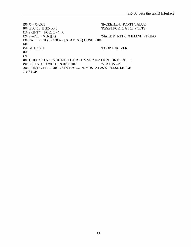
SR400 with the GPIB Interface
55
390 X = X+.005 'INCREMENT PORT1 VALUE 400 IF X>10 THEN X=0 'RESET PORT1 AT 10 VOLTS 410 PRINT " PORT1 = "; X 420 P$=P1$ + STR$(X) 'MAKE PORT1 COMMAND STRING 430 CALL SEND(SR400%,P$,STATUS%):GOSUB 480 440 ' 450 GOTO 300 'LOOP FOREVER 460 ' 470 ' 480 'CHECK STATUS OF LAST GPIB COMMUNICATION FOR ERRORS 490 IF STATUS%=0 THEN RETURN 'STATUS OK 500 PRINT "GPIB ERROR STATUS CODE = ";STATUS% 'ELSE ERROR 510 STOP

SR400 with the GPIB Interface
56
PROGRAM EXAMPLE 4: IBM PC, MICROSOFT C V4.0, VIA GPIB This program requires the Capital Equipment Corporation GPIB card for the IBM PC. It has firmware in ROM to interface high level languages to the GPIB. The header file MS-C488.H contains definitions of all of the CEC firmware routines which can be called from C. Note that the order of arguments in the calls are reversed from those used by BASIC. To use these routines, the large model must be used. Compile with the /AL/Ze switch and link with GPIB-L.OBJ (on the CEC disk). /* Compile with >MSC program name/AL/Ze; link with GPIB-L.OBJ (on CEC disk) include MS-C488.H MS-C488.H defines all of the CEC firmware routines so that they can be called from a C program. Remember that the order of the arguments is REVERSED from the BASIC calls described in the manual. Example program to read the SR400 counter data and ramp the PORT1 analog output using Microsoft C v4.0 (large model) and the Capital Equipment Corp. GPIB interface card. Set the SR400 for GPIB ADDR=23. */ #include <ms-c488.h> #include <stdio.h> char result[80]; main() int i,status,sr400=23; int my_address=21, system_controller=0; char cmd[80], portstr[40]; long n1; float x; initialize(&system_controller, &my_address); /* init GPIB controller */ /* clear SR400 */ transmit(&status, "IFC UNT UNL REN MTA LISTEN 23 SDC"); Statcheck(status); for (i=0;i<1000;i++); /* wait for clear to finish */ /* set counter A to 10 Mhz */ TxGpib(sr400,"CI0,0");
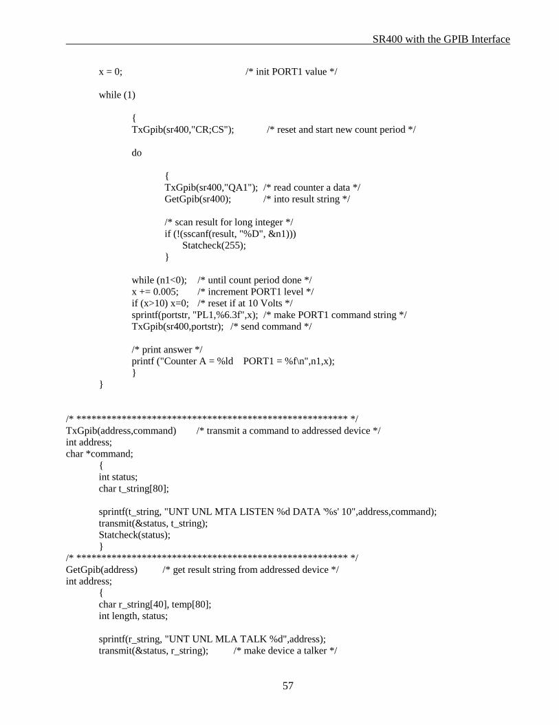
SR400 with the GPIB Interface
57
x = 0; /* init PORT1 value */ while (1) TxGpib(sr400,"CR;CS"); /* reset and start new count period */ do TxGpib(sr400,"QA1"); /* read counter a data */ GetGpib(sr400); /* into result string */ /* scan result for long integer */ if (!(sscanf(result, "%D", &n1))) Statcheck(255); while (n1<0); /* until count period done */ x += 0.005; /* increment PORT1 level */ if (x>10) x=0; /* reset if at 10 Volts */ sprintf(portstr, "PL1,%6.3f",x); /* make PORT1 command string */ TxGpib(sr400,portstr); /* send command */ /* print answer */ printf ("Counter A = %ld PORT1 = %f\n",n1,x); /* ****************************************************** */ TxGpib(address,command) /* transmit a command to addressed device */ int address; char *command; int status; char t_string[80]; sprintf(t_string, "UNT UNL MTA LISTEN %d DATA '%s' 10",address,command); transmit(&status, t_string); Statcheck(status); /* ****************************************************** */ GetGpib(address) /* get result string from addressed device */ int address; char r_string[40], temp[80]; int length, status; sprintf(r_string, "UNT UNL MLA TALK %d",address); transmit(&status, r_string); /* make device a talker */
SR400 with the GPIB Interface
58
Statcheck(status); strcpy(temp, " "); /* clear result string */ receive(&status, &length, temp); /* get answer */ Statcheck(status); strcpy(result, temp); /* move answer into global result string */ /* ****************************************************** */ Statcheck(status) /* check GPIB status */ int status; if (status) printf("GPIB error: status = %d",status); exit();

Troubleshooting
59
TROUBLESHOOTING To start, make sure that the power entry module on the rear panel is set for the ac line voltage in your area and that the correct fuse is installed. The selected ac voltage may be seen through the window on the power entry module. Verify that the line cord is plugged all the way into the power entry module and that the power button on the front panel is pressed in. LCD CONTRAST If there are no characters on the LCD, or the contrast is very poor, go to the LCD CONTRAST line of the SETUP menu and use the spin knob to adjust the contrast. Larger values increase the contrast. FAN The fan in the SR400 is temperature controlled. When the unit is cold, the fan is off. When the internal temperature reaches about 30° C, the fan starts to blow. Do not block the vents in the chassis or the unit may not operate properly. FRONT PANEL TEST The keyboard, knob, display, and LED indicators may be tested in the front panel test mode. Turn the unit on while holding down the COM key to enter the front panel test. The LCD should display the message FRONT PANEL TEST. Pressing a key will cause the LCD to display the name of the key on both lines of the display. If the keys do not work properly, check to make sure that there are no keys stuck in the down position. Turning the knob will light each LED one at a time in succession across the front panel. POWER ON RESET If the instrument turns on with odd combinations of LED's on, a garbled message on the LCD, or is unresponsive to the keyboard or knob, then the memory contents may have been corrupted causing the instrument to "hang". To remedy the situation, turn the unit off and hold down the STOP key while turning the unit back on. This
causes the unit to reinitialize the memory and assume the default setup. QUICK TEST Unplug all cables from the unit and recall the default setup by holding the STOP key down while turning the unit on. The message RECALL DEFAULT should appear on the display for ~3 s. Press the DOWN key once to go to the A=INPUT 1 menu line. Rotate the knob until A=10 MHz appears on the menu line. To start a count period, press the START key once. The data display should show counting in counter A for 1 second and stop at A= 10000000. Counter A will have counted the internal 10 MHz timebase for 1 second and reached 10,000,000 counts. To reset the counter, press the STOP key. The data display should reset to 0. Now press the DOWN key 3 more times to display the N PERIODS line. Rotate the knob until N PERIODS=10. Start a scan by pressing the START key. The counter should cycle through 10 count periods separated by the default dwell time (1 s). The display shows the current scan position in brackets. Reset the scan using the STOP key. Start another scan with the START key but press the STOP key before all 10 count periods are completed. This pauses the scan at the last completed count period. START will resume the scan and STOP will reset the scan. In general, if the START key doesn't start a count period it is because the counters are paused at the end of a scan. In this case, the SCAN led will be off and the N PERIODS display shows that the programmed number of points has been taken. A STOP is required to reset the scan. Pressing the STOP key twice in succession always resets the counters.

Troubleshooting
60
COUNTING There are several reasons why a counter may not seem to be counting correctly. 1) Counting is not enabled. The COUNT led
does not turn on when the START key is pressed. This is because the counters need to be reset. Use the STOP key to reset the counters. Verify that the preset count period is long enough so that a nonzero count can occur.
2) The counter input is set to the wrong source or
input. Check the counter input menu line and the counter discriminator output for the correct signal. If the preset counter has no input, then the count period will never terminate.
3) The counter is gated. If the count led is on and
the source is correct but no counting occurs, the counter gate may be disabling the counter. Check that the gate is in CW mode if no gating is needed or, if gating is required, that the trigger is connected and discriminating correctly. The gate may be viewed through the GATE output. The output is low when the gate enables the counter.
4) Incorrect gate position. When nanosecond gate
delays or widths are used, timing accuracy is critical. Gate timing should be verified by viewing the DISC and GATE outputs on an oscilloscope. Be sure to use equal length cables so as not to introduce timing skew. The timing accuracy of the outputs from the SR400 is 2 ns.
5) Bad gate triggering. The trigger input may not be discriminated correctly. Check the trigger slope and level. The discriminated trigger pulses may be viewed through the T DISC output when the input to counter T is TRIG. Double triggering or the wrong slope can cause erroneous gates.
6) Incorrect discriminator levels or slopes. Verify
that the discriminator settings are correct. Use the DISC output to check the discriminator output pulses on an oscilloscope.
7) Signal inputs are overloaded. Check that the
inputs are <±300 mV or, if the signal exceeds 300 mV, that the overloads do not last longer than 10 µs. If the overload lasts longer than 10 µs, the input amplifiers will not recover for about 200 ns.
8) Discriminators are inhibited. Check that the
INHIBIT input on the rear panel is not held at TTL high. Leave the INHIBIT input unconnected when not in use.
9) EXT STOP is resetting the counters. If the
DWELL TIME is programmed (i.e. not EXTERNAL) an EXT STOP will reset the counters. In general, EXT STOP should be disconnected when the DWELL TIME is NOT EXTERNAL.
10) The DWELL TIME is EXTERNAL and EXT
START and STOP are disconnected or connected to the wrong signal sources.
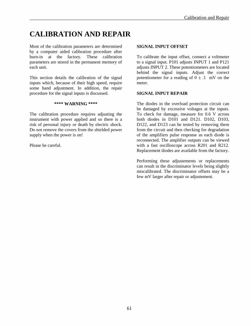
Calibration and Repair
61
CALIBRATION AND REPAIR Most of the calibration parameters are determined by a computer aided calibration procedure after burn-in at the factory. These calibration parameters are stored in the permanent memory of each unit. This section details the calibration of the signal inputs which, because of their high speed, require some hand adjustment. In addition, the repair procedure for the signal inputs is discussed.
**** WARNING **** The calibration procedure requires adjusting the instrument with power applied and so there is a risk of personal injury or death by electric shock. Do not remove the covers from the shielded power supply when the power is on! Please be careful.
SIGNAL INPUT OFFSET To calibrate the input offset, connect a voltmeter to a signal input. P101 adjusts INPUT 1 and P121 adjusts INPUT 2. These potentiometers are located behind the signal inputs. Adjust the correct potentiometer for a reading of 0 ± .1 mV on the meter. SIGNAL INPUT REPAIR The diodes in the overload protection circuit can be damaged by excessive voltages at the inputs. To check for damage, measure for 0.6 V across both diodes in D101 and D121. D102, D103, D122, and D123 can be tested by removing them from the circuit and then checking for degradation of the amplifiers pulse response as each diode is reconnected. The amplifier outputs can be viewed with a fast oscilloscope across R201 and R212. Replacement diodes are available from the factory. Performing these adjustements or replacements can result in the discriminator levels being slightly miscalibrated. The discriminator offsets may be a few mV larger after repair or adjustement.

Calibration and Repair
62
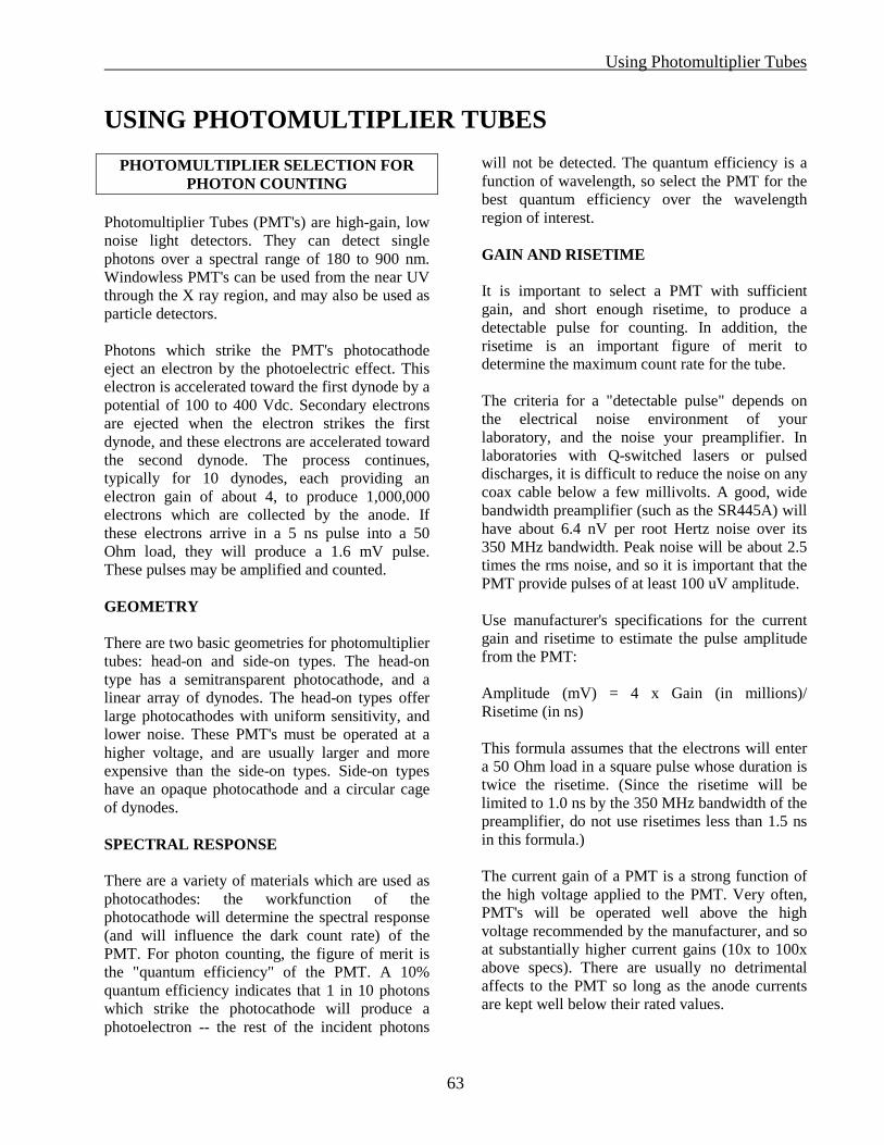
Using Photomultiplier Tubes
63
USING PHOTOMULTIPLIER TUBES
PHOTOMULTIPLIER SELECTION FOR PHOTON COUNTING
Photomultiplier Tubes (PMT's) are high-gain, low noise light detectors. They can detect single photons over a spectral range of 180 to 900 nm. Windowless PMT's can be used from the near UV through the X ray region, and may also be used as particle detectors. Photons which strike the PMT's photocathode eject an electron by the photoelectric effect. This electron is accelerated toward the first dynode by a potential of 100 to 400 Vdc. Secondary electrons are ejected when the electron strikes the first dynode, and these electrons are accelerated toward the second dynode. The process continues, typically for 10 dynodes, each providing an electron gain of about 4, to produce 1,000,000 electrons which are collected by the anode. If these electrons arrive in a 5 ns pulse into a 50 Ohm load, they will produce a 1.6 mV pulse. These pulses may be amplified and counted. GEOMETRY There are two basic geometries for photomultiplier tubes: head-on and side-on types. The head-on type has a semitransparent photocathode, and a linear array of dynodes. The head-on types offer large photocathodes with uniform sensitivity, and lower noise. These PMT's must be operated at a higher voltage, and are usually larger and more expensive than the side-on types. Side-on types have an opaque photocathode and a circular cage of dynodes. SPECTRAL RESPONSE There are a variety of materials which are used as photocathodes: the workfunction of the photocathode will determine the spectral response (and will influence the dark count rate) of the PMT. For photon counting, the figure of merit is the "quantum efficiency" of the PMT. A 10% quantum efficiency indicates that 1 in 10 photons which strike the photocathode will produce a photoelectron -- the rest of the incident photons
will not be detected. The quantum efficiency is a function of wavelength, so select the PMT for the best quantum efficiency over the wavelength region of interest. GAIN AND RISETIME It is important to select a PMT with sufficient gain, and short enough risetime, to produce a detectable pulse for counting. In addition, the risetime is an important figure of merit to determine the maximum count rate for the tube. The criteria for a "detectable pulse" depends on the electrical noise environment of your laboratory, and the noise your preamplifier. In laboratories with Q-switched lasers or pulsed discharges, it is difficult to reduce the noise on any coax cable below a few millivolts. A good, wide bandwidth preamplifier (such as the SR445A) will have about 6.4 nV per root Hertz noise over its 350 MHz bandwidth. Peak noise will be about 2.5 times the rms noise, and so it is important that the PMT provide pulses of at least 100 uV amplitude. Use manufacturer's specifications for the current gain and risetime to estimate the pulse amplitude from the PMT: Amplitude (mV) = 4 x Gain (in millions)/ Risetime (in ns) This formula assumes that the electrons will enter a 50 Ohm load in a square pulse whose duration is twice the risetime. (Since the risetime will be limited to 1.0 ns by the 350 MHz bandwidth of the preamplifier, do not use risetimes less than 1.5 ns in this formula.) The current gain of a PMT is a strong function of the high voltage applied to the PMT. Very often, PMT's will be operated well above the high voltage recommended by the manufacturer, and so at substantially higher current gains (10x to 100x above specs). There are usually no detrimental affects to the PMT so long as the anode currents are kept well below their rated values.

Typical Experiment
64
Conclusions: Select a PMT with a risetime < 3 ns and a current gain > 5 million. DARK COUNTS PMT's are the quietest detectors available. The primary noise source is thermionic emission of electrons from the photocathode and from the first few dynodes of the electron multiplier. PMT housings which cool the PMT to about -20° C can dramatically reduce the dark count ( from a few kHz to a few Hz). The residual counts arise from radioactive decays of materials inside the PMT and from cosmic rays. PMT's which are specifically designed for photon counting will specify their noise in terms of the rate of output pulses whose amplitudes exceed some fraction of a pulse from a single photon. More often, the noise is specified as an anode dark current. Assuming the primary source of dark current is thermionic emission from the photocathode, the dark count rate is given by : Dark Count (in kHz) = 6 x Dark Current (in nA) / Gain (in millions)
PMT BASE DESIGN PMT bases which are designed for general purpose applications are not appropriate for photon counting. General purpose bases will not allow high count rates, and often cause problems such as double counting and poor plateau characteristics. A PMT base with the proper high voltage taper, bypassing, snubbing, and shielding is required for premium photon counting performance.
CAUTION: Lethal High Voltages are used in PMT applications. Use extreme caution when working with these devices. Only those experienced with high voltage circuits should attempt any of these procedures. Never work alone. DYNODE BIASING A PMT base provides bias voltages to the PMT's photocathode and dynodes from a single negative high voltage power supply. The simplest design consists of a resistive voltage divider, as shown in Figure A. In this configuration the voltage between each dynode, and so the current gain at each dynode, is the same. Typical current gains are 3 to 4, and so there will typically be 3 to 4 electrons leaving the first dynode, with a variance of about 2 electrons. This large relative variance (due to the small number of ejected electrons) gives rise to a large variations in the pulse height of the detected signal. Since statistical fluctuations in pulse height are caused by the low gain of the first few stages of the multiplier chain, increasing the gain of these stages will reduce pulse height variations and so improve the plateau characteristics of the PMT. To increase the gain of the first few stages, the resistor values in the bias chain are tapered to increase the voltage in the front end of the multiplier chain. The resistor values are slowly tapered so that the electrostatic focusing of electrons in the multiplier chain is not adversely affected.

Using Photomultiplier Tubes
65
Current for the electron multiplier is provided by the bias network. Current drawn from the bias network will cause the dynode potentials to change, and so change the tube gain. This problem is of special concern in lifetime measurements. The shape of exponential decay curves will be changed if the tube gain varies with count rate. To be certain that this is not a problem, repeat the measurement at half the original intensity. The problem of gain variation with count rate is avoided if the current in the bias network is about 20 times the output current from the PMT's anode. Example: If a PMT is operated so that it gives 20 mV pulses of 5 ns duration into a 50 Ohm cable, then the average current at 50 MHz count rate will be 0.1 mA. If the bias resistors are chosen so that the chain current is 20 x 0.1 mA = 2 mA, then the PMT's gain will remain constant vs. count rate. If this PMT is operated at 2500 vdc, then the power dissipated in this base is 5 Watts. There are a few other methods to avoid this problem which do not require high bias currents. These methods depend on the fact that the majority of the output current is drawn from the last few dynodes of the multiplier. (1) Replace the last few resistors in the bias chain with Zener Diodes. As long as there is some reverse current through a Zener, the voltage across the diodes is nearly constant. This will prevent the
voltage on these stages from dropping as the output current is increased. (2) Use external power supplies for the last few dynodes in the multiplier chain. This approach dissipates the least amount of electrical power since the majority of the output current comes from lower voltage power supplies, however it is the most difficult to implement. (3) If the average count rate is low, but the peak count rate is high, then bypass capacitors on the last few stages may be used to prevent the dynode voltage from dropping. ( Use 20x the average output current for the chain current.) For a voltage drop of less than 1%, the stored charge on the last bypass capacitor should be 100x the charge output during the peak count rate. For example, the charge output during a 1 ms burst of a 100 MHz count rate, each with an amplitude of 10 mV into 50 Ohms and a pulse width of 5 ns, is 0.1 uC. If the voltage on the last dynode is 200 Vdc, then the bypass capacitor for the last dynode should have a value given by: C = 100 Q/V = 100 x 0.1uC / 200V = 0.05 uF The current from higher dynodes is smaller so the capacitors bypassing these stages may be smaller. Only the final four or five dynodes need to be bypassed, usually with a capacitor which has half the capacitance of the preceding stage. To reduce the voltage requirement for these capacitors, they
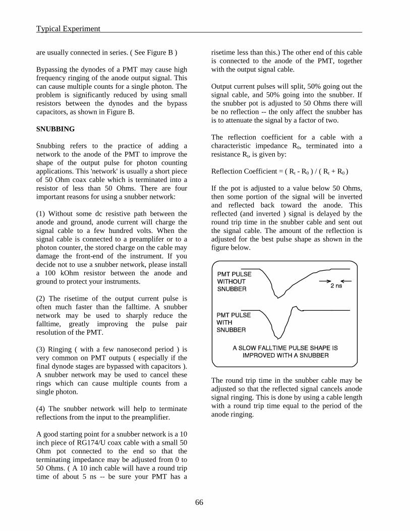
Typical Experiment
66
are usually connected in series. ( See Figure B ) Bypassing the dynodes of a PMT may cause high frequency ringing of the anode output signal. This can cause multiple counts for a single photon. The problem is significantly reduced by using small resistors between the dynodes and the bypass capacitors, as shown in Figure B. SNUBBING Snubbing refers to the practice of adding a network to the anode of the PMT to improve the shape of the output pulse for photon counting applications. This 'network' is usually a short piece of 50 Ohm coax cable which is terminated into a resistor of less than 50 Ohms. There are four important reasons for using a snubber network: (1) Without some dc resistive path between the anode and ground, anode current will charge the signal cable to a few hundred volts. When the signal cable is connected to a preamplifer or to a photon counter, the stored charge on the cable may damage the front-end of the instrument. If you decide not to use a snubber network, please install a 100 kOhm resistor between the anode and ground to protect your instruments. (2) The risetime of the output current pulse is often much faster than the falltime. A snubber network may be used to sharply reduce the falltime, greatly improving the pulse pair resolution of the PMT. (3) Ringing ( with a few nanosecond period ) is very common on PMT outputs ( especially if the final dynode stages are bypassed with capacitors ). A snubber network may be used to cancel these rings which can cause multiple counts from a single photon. (4) The snubber network will help to terminate reflections from the input to the preamplifier. A good starting point for a snubber network is a 10 inch piece of RG174/U coax cable with a small 50 Ohm pot connected to the end so that the terminating impedance may be adjusted from 0 to 50 Ohms. ( A 10 inch cable will have a round trip time of about 5 ns -- be sure your PMT has a
risetime less than this.) The other end of this cable is connected to the anode of the PMT, together with the output signal cable. Output current pulses will split, 50% going out the signal cable, and 50% going into the snubber. If the snubber pot is adjusted to 50 Ohms there will be no reflection -- the only affect the snubber has is to attenuate the signal by a factor of two. The reflection coefficient for a cable with a characteristic impedance R0, terminated into a resistance Rt, is given by: Reflection Coefficient = ( Rt - R0 ) / ( Rt + R0 ) If the pot is adjusted to a value below 50 Ohms, then some portion of the signal will be inverted and reflected back toward the anode. This reflected (and inverted ) signal is delayed by the round trip time in the snubber cable and sent out the signal cable. The amount of the reflection is adjusted for the best pulse shape as shown in the figure below.
The round trip time in the snubber cable may be adjusted so that the reflected signal cancels anode signal ringing. This is done by using a cable length with a round trip time equal to the period of the anode ringing.
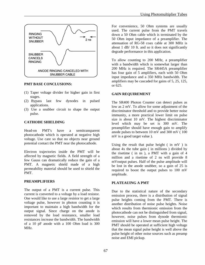
Using Photomultiplier Tubes
67
PMT BASE CONCLUSIONS: (1) Taper voltage divider for higher gain in first
stages. (2) Bypass last few dynodes in pulsed
applications. (3) Use a snubber circuit to shape the output
pulse. CATHODE SHIELDING Head-on PMT's have a semitransparent photocathode which is operated at negative high voltage. Use care so that no objects near ground potential contact the PMT near the photocathode. Electron trajectories inside the PMT will be affected by magnetic fields. A field strength of a few Gauss can dramatically reduce the gain of a PMT. A magnetic shield made of a high permeability material should be used to shield the PMT. PREAMPLIFIERS The output of a PMT is a current pulse. This current is converted to a voltage by a load resistor. One would like to use a large resistor to get a large voltage pulse, however in photon counting it is important to maintain a high bandwidth for the output signal. Since charge on the anode is removed by the load resistance, smaller load resistances increase the bandwidth. The bandwidth of a 10 pF anode with a 100 Ohm load is 300 MHz.
For convenience, 50 Ohm systems are usually used. The current pulse from the PMT travels down a 50 Ohm cable which is terminated by the 50 Ohm input impedance of a preamplifier. The attenuation of RG-58 coax cable at 300 MHz is about 1 dB/ 10 ft. and so it does not significantly degrade performance in this application. To allow counting to 200 MHz, a preamplifier with a bandwidth which is somewhat larger than 200 MHz is required. The SR445A preamplifier has four gain of 5 amplifiers, each with 50 Ohm input impedance and a 350 MHz bandwidth. The amplifiers may be cascaded for gains of 5, 25, 125, or 625. GAIN REQUIREMENT The SR400 Photon Counter can detect pulses as low as 2 mV. To allow for some adjustment of the discriminator threshold and to provide better noise immunity, a more practical lower limit on pulse size is about 10 mV. The highest discriminator level which may be set is 300 mV. The preamplifier should have enough gain to amplify anode pulses to between 10 mV and 300 mV ( 100 mV is a good target value ). Using the result that pulse height ( in mV ) is about 4x the tube gain ( in millions ) divided by the risetime ( in ns ), a PMT with a gain of 4 million and a risetime of 2 ns will provide 8 mVoutput pulses. Half of the pulse amplitude will be lost in the anode snubber, so a gain of 25 is required to boost the output pulses to 100 mV amplitude. PLATEAUING A PMT Due to the statistical nature of the secondary emission process, there is a distribution of signal pulse heights coming from the PMT. There is another distribution of noise pulse heights. Noise which results from thermionic emission from the photocathode can not be distinguished from signal, however, noise pulses from dynode thermionic emission will have a lower mean pulse height. The PMT should be operated at sufficient high voltage that the mean signal pulse height is well above the pulse height of other noise sources such as preamp noise and EMI pickup.

Typical Experiment
68
There are two reasons for carefully selecting the input discriminator level. The first is to improve the signal-to-noise ratio by setting the discriminator level above most of the noise pulses, but below most of the signal pulses. The second reason is to reduce drift: if the discriminator threshold is set to the middle of the signal pulse height distribution, then small changes in the tube gain can cause a large change in the count rate. There is no exact prescription for setting the discriminator threshold: the procedure used will depend somewhat on the nature of the measurement. If dark counts are a problem then the discriminator level should be set higher than when drift is a concern. If the PMT is cooled ( reducing thermionic emission ) then a lower discriminator level is probably okay. If the PMT has a ring on the anode signal then the discriminator level should be set high enough so that the rings are not counted. THE 'CORRECT' WAY The tube should be operated at the maximum high voltage recommended by the manufacturer. Use enough preamplifier gain so that the single photon pulse height is about 100 mV. Provide enough light to the PMT for a count rate of a few megahertz. Using a 300 MHz oscilloscope, adjust the snubber termination for minimum ringing on the anode signal. Take the pulse height spectrum of the anode signal. This is very time consuming and involves recording the count difference between successive discriminator steps and plotting the result Vs discriminator value. If the PMT dark count rate is a concern, then you will also need to take the pulse height spectrum of the dark count signal. It will take much longer to take the dark count spectrum because the count rate should be much lower. The object is to find a discriminator level which is higher than the mean noise pulse height, and below the mean signal pulse height.
THE 'FAST AND PRETTY GOOD' WAY This technique works very well and is particularly suited for those who do not want to make a career out of plateauing their PMT's. The PMT should be operated at (or a bit above) the recommended maximum high voltage. Provide enough illumination for a count rate of a few megahertz, and enough preamp gain to get pulse heights of about 100 mV. Using a 300 MHz oscilloscope, adjust the snubber termination impedance for the best pulse shape. Look carefully at the anode pulse shape and set the discriminator to a level which is above any ringing, but well below the mean pulse height. If there is lots of EMI or amplifier noise then increase the PMT's high voltage to increase the signal pulse height.
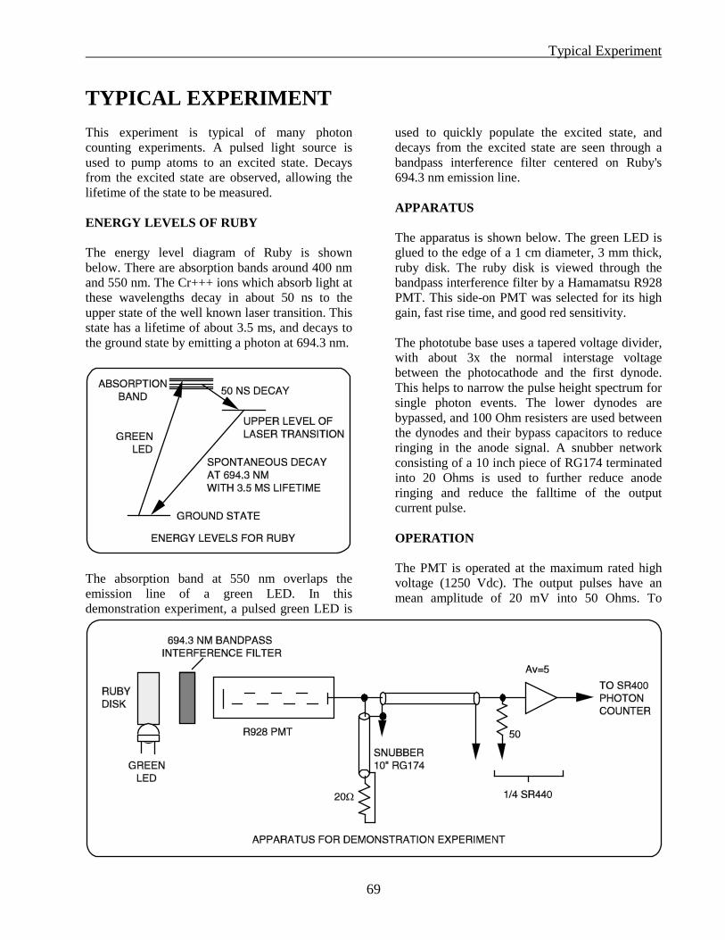
Typical Experiment
69
TYPICAL EXPERIMENT This experiment is typical of many photon counting experiments. A pulsed light source is used to pump atoms to an excited state. Decays from the excited state are observed, allowing the lifetime of the state to be measured. ENERGY LEVELS OF RUBY The energy level diagram of Ruby is shown below. There are absorption bands around 400 nm and 550 nm. The Cr+++ ions which absorb light at these wavelengths decay in about 50 ns to the upper state of the well known laser transition. This state has a lifetime of about 3.5 ms, and decays to the ground state by emitting a photon at 694.3 nm.
The absorption band at 550 nm overlaps the emission line of a green LED. In this demonstration experiment, a pulsed green LED is
used to quickly populate the excited state, and decays from the excited state are seen through a bandpass interference filter centered on Ruby's 694.3 nm emission line. APPARATUS The apparatus is shown below. The green LED is glued to the edge of a 1 cm diameter, 3 mm thick, ruby disk. The ruby disk is viewed through the bandpass interference filter by a Hamamatsu R928 PMT. This side-on PMT was selected for its high gain, fast rise time, and good red sensitivity. The phototube base uses a tapered voltage divider, with about 3x the normal interstage voltage between the photocathode and the first dynode. This helps to narrow the pulse height spectrum for single photon events. The lower dynodes are bypassed, and 100 Ohm resisters are used between the dynodes and their bypass capacitors to reduce ringing in the anode signal. A snubber network consisting of a 10 inch piece of RG174 terminated into 20 Ohms is used to further reduce anode ringing and reduce the falltime of the output current pulse. OPERATION The PMT is operated at the maximum rated high voltage (1250 Vdc). The output pulses have an mean amplitude of 20 mV into 50 Ohms. To
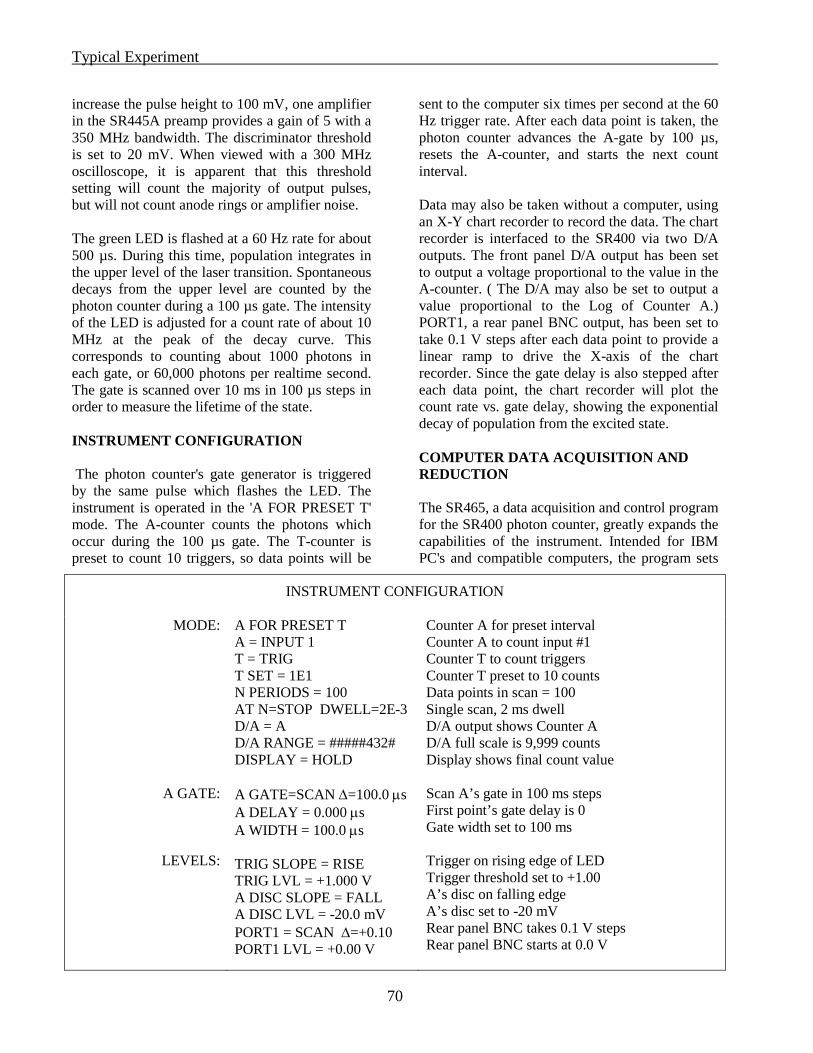
Typical Experiment
70
increase the pulse height to 100 mV, one amplifier in the SR445A preamp provides a gain of 5 with a 350 MHz bandwidth. The discriminator threshold is set to 20 mV. When viewed with a 300 MHz oscilloscope, it is apparent that this threshold setting will count the majority of output pulses, but will not count anode rings or amplifier noise. The green LED is flashed at a 60 Hz rate for about 500 µs. During this time, population integrates in the upper level of the laser transition. Spontaneous decays from the upper level are counted by the photon counter during a 100 µs gate. The intensity of the LED is adjusted for a count rate of about 10 MHz at the peak of the decay curve. This corresponds to counting about 1000 photons in each gate, or 60,000 photons per realtime second. The gate is scanned over 10 ms in 100 µs steps in order to measure the lifetime of the state. INSTRUMENT CONFIGURATION The photon counter's gate generator is triggered by the same pulse which flashes the LED. The instrument is operated in the 'A FOR PRESET T' mode. The A-counter counts the photons which occur during the 100 µs gate. The T-counter is preset to count 10 triggers, so data points will be
sent to the computer six times per second at the 60 Hz trigger rate. After each data point is taken, the photon counter advances the A-gate by 100 µs, resets the A-counter, and starts the next count interval. Data may also be taken without a computer, using an X-Y chart recorder to record the data. The chart recorder is interfaced to the SR400 via two D/A outputs. The front panel D/A output has been set to output a voltage proportional to the value in the A-counter. ( The D/A may also be set to output a value proportional to the Log of Counter A.) PORT1, a rear panel BNC output, has been set to take 0.1 V steps after each data point to provide a linear ramp to drive the X-axis of the chart recorder. Since the gate delay is also stepped after each data point, the chart recorder will plot the count rate vs. gate delay, showing the exponential decay of population from the excited state. COMPUTER DATA ACQUISITION AND REDUCTION The SR465, a data acquisition and control program for the SR400 photon counter, greatly expands the capabilities of the instrument. Intended for IBM PC's and compatible computers, the program sets
INSTRUMENT CONFIGURATION
MODE:
A GATE:
LEVELS:
A FOR PRESET T A = INPUT 1 T = TRIG T SET = 1E1 N PERIODS = 100 AT N=STOP DWELL=2E-3 D/A = A D/A RANGE = #####432# DISPLAY = HOLD A GATE=SCAN ∆=100.0 µs A DELAY = 0.000 µs A WIDTH = 100.0 µs TRIG SLOPE = RISE TRIG LVL = +1.000 V A DISC SLOPE = FALL A DISC LVL = -20.0 mV PORT1 = SCAN ∆=+0.10 PORT1 LVL = +0.00 V
Counter A for preset interval Counter A to count input #1 Counter T to count triggers Counter T preset to 10 counts Data points in scan = 100 Single scan, 2 ms dwell D/A output shows Counter A D/A full scale is 9,999 counts Display shows final count value Scan A’s gate in 100 ms steps First point’s gate delay is 0 Gate width set to 100 ms Trigger on rising edge of LED Trigger threshold set to +1.00 A’s disc on falling edge A’s disc set to -20 mV Rear panel BNC takes 0.1 V steps Rear panel BNC starts at 0.0 V
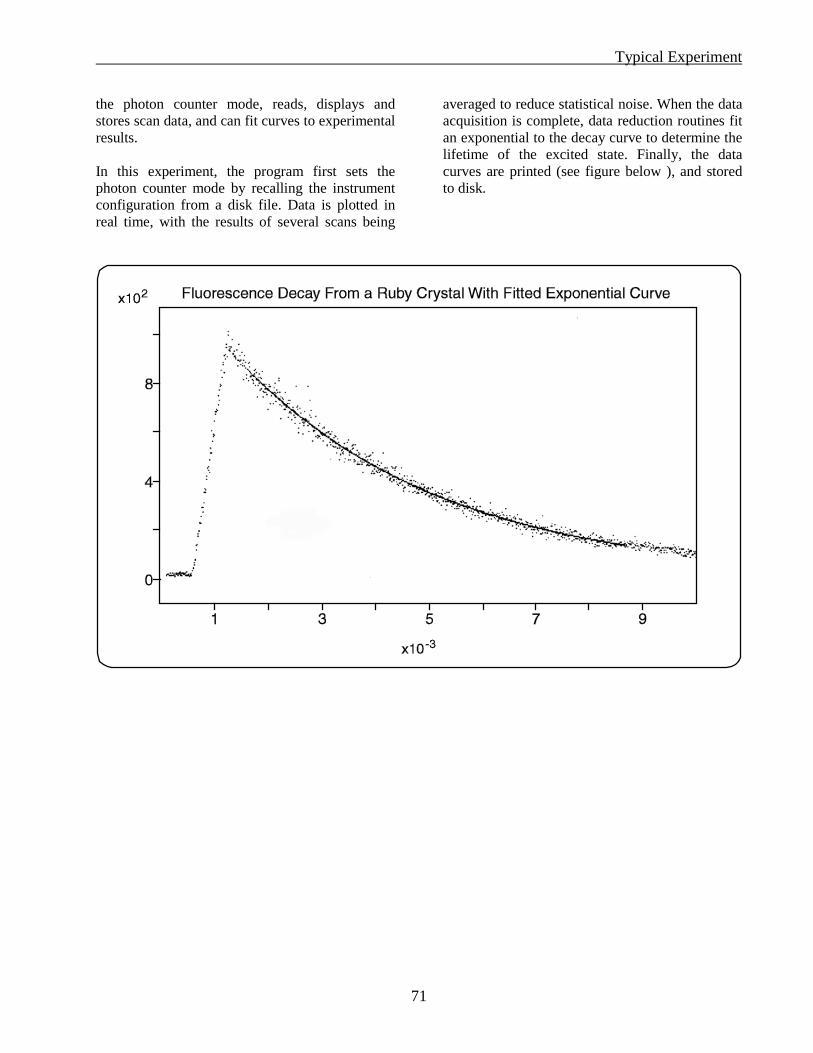
Typical Experiment
71
the photon counter mode, reads, displays and stores scan data, and can fit curves to experimental results. In this experiment, the program first sets the photon counter mode by recalling the instrument configuration from a disk file. Data is plotted in real time, with the results of several scans being
averaged to reduce statistical noise. When the data acquisition is complete, data reduction routines fit an exponential to the decay curve to determine the lifetime of the excited state. Finally, the data curves are printed (see figure below ), and stored to disk.

Typical Experiment
72
SR400 Circuit Description
73
SR400 CIRCUIT DESCRIPTION The SR400 has five printed circuit boards. Almost all of the components are located on the main circuit board, including the microprocessor and interfaces, fast counters and discriminators, gate generators, and digital to analog conversion circuits. There is one circuit board in the power supply enclosure. The other three circuit boards are much smaller and are mounted to the front panel. They hold the 2 line by 24 character LCD display, the key pad, and the status LED indicators.
MICROPROCESSOR CONTROL MICROPROCESSOR SYSTEM (sheet 12) The microprocessor, U1206, is a Z8800 (Super 8) microcontroller which integrates a fast processor, UART, counter-timers, interrupt controller, DMA controller, and RAM into one VLSI component. This high degree of integration is essential to the performance of the SR400. The Super 8 is clocked by the 20 MHz crystal time base oscillator. The data bus is multiplexed with the lower 8 bits of the address bus. U1207 latches the address bits at the start of every memory cycle. The firmware and calibration bytes are stored in the 32K x 8 UVEPROM, U1208. U1209 is a 32K x 8 CMOS static RAM. The large RAM allows large scans (up to 2000 points) to be internally buffered. The RAM is battery backed up allowing instrument settings to be saved. Q1201-3 perform power-up and power-down reset and RAM protection. I/O port strobes are generated by U1201 and U1211, RD and WR are decoded by U1203. RS-232 INTERFACE (sheet 12) The Super 8 has an on-chip UART and baud rate generator. U1205 level shifts and buffers the signals to the external connector. The connector is a data communications equipment (DCE) type. The baud rate is derived from the processor clock. Any standard baud rate from 300 to 19.2K baud may be programmed.
GPIB INTERFACE (sheet 13) The GPIB (IEEE-488) interface is provided by the TMS9914A controller, U1311. U1309 and U1310 buffer data I/O to the GPIB connector. U1311 is programmed to interrupt to the processor whenever there is bus activity addressed to the SR400. INPUT PORTS (sheet 13) U1301 and U1302 read the prescale bits from counters A and B. They are latched by CTR_1 to provide unambiguous data while the counters are counting. U1303 is the keyboard input buffer. The upper bits of U1301-3 are used to read various status signals. SLOW COUNTERS (sheet 13) U1304-8 are 5 MHz 8253 VLSI counters. Each chip has 3 multi-mode 16 bit counters. These counters count the middle bits in counters A,B, and T, the gate delay and width oscillators, and the crystal time base for the dwell time. OUTPUT PORTS (sheet 14) U1401-1406 are 8 bit data latches. U1401, U1402, and U1406 provide control bits for the discriminators, counters, and gates. U1403 holds the preset value for the T counter. U1404 and U1405 drive the front panel LED indicators and keyboard strobes. FRONT PANEL (sheets 12,13,14,16) The front panel is connected to the main board through 5 cables. The knob is an optical encoder buffered by U1202. Each transition of its outputs interrupts the processor which keeps track of its direction and speed. The LCD display connects directly to the processor data bus. Besides the 8 data lines, there

Typical Experiment
74
are 2 address lines, chip select, power and ground, and display contrast control. The electroluminescent backlight requires a 100 Vac, 100 Hz signal. This power is derived from the dc power supplies and is isolated from the ac main. The status LED indicators are driven by U1405. The key pad is strobed by U1405 and read by U1303. DIGITAL TO ANALOG CONVERTER (sheet 15) U1502 is a 12-bit D/A converter which is loaded 4 bits at a time by the processor. The voltage output from 4/4 U1504 is 0 to -10.24 Vdc. The rest of U1504 shifts and attenuates this output to provide control voltages. These analog outputs are multiplexed onto 20 sample and hold amplifiers. Each S/H is refreshed every 2 ms. U1503 multiplexes the gate generator calibration voltages. U1506 multiplexes the gate adjustment voltages as well as the analog outputs and the LCD contrast. U1501 provides the discriminator thresholds.
FAST COUNTERS SIGNAL INPUTS (sheet 1) Signal inputs INPUT 1 and INPUT 2 pass through amplifiers AMP 1 and AMP 2. These are dc to 300 MHz, gain of 5 amplifiers. They have a 1.2 ns rise/fall time, ± 300 mV input range, and a 4 ns recovery time from a 20X overload. The inputs are protected to ± 5Vdc and ± 50V transients. The following is a brief description of amplifier AMP 1. AMP 2 is identical. R102, R103, R104, P101, D101, D102, and D103 comprise an overload protection circuit which clamps the inputs to the amplifiers at ± .35 V. Ac gain is provided by Q101 and Q102 and is compensated by C107. U101 sets the amplifier's dc gain. Q102 sums the ac and dc signals and can drive its 100 Ω output to ± 2 V. U102, D130, and Q130 provide a
temperature compensated bias voltage for the overload protection circuits which is adjusted by P101 to null the dc offset at the input. DISCRIMINATORS (sheet 2) Comparators U202, U203, U204, U209 discriminate the AMP 1 and AMP 2 outputs into ECL levels. U202 is the A discriminator when the input to counter A is INPUT 1. The threshold is provided by analog voltage A_DISC and buffered by 1/4 U208. The output transistor, 1/4 U207, provides a high frequency, low impedance output. The comparator is operated in the Schmitt trigger configuration with about 20 mV of hysteresis. Since the input signal has been amplified by 5, this represents about 4 mV of hysteresis at the input. Control signal A_POL inverts the comparator output in 1/4 U1206 if the discriminator slope is set to FALL. U203 is the B discriminator when the input to counter B is INPUT 1. If the input to counter B is INPUT 2, U209 is the B discriminator. Operation is identical to the A discriminator except that the outputs of U203 and U209 are multiplexed through U210. The B_SEL line selects the appropriate output and B_POL programs the slope. U204 is the T discriminator when the input to counter T is INPUT 2. The comparators may be inhibited by the DISC_INH signal which is derived from the INHIBIT input on the rear panel. When DISC_INH is asserted, the comparators will be inactive and their outputs frozen. U201 is the gate trigger discriminator. It operates like the input discriminators except that it has about 75 mV of hysteresis. A AND B COUNTERS (sheets 3 and 5) There are 2 gated counting channels capable of 220 MHz operation and essentially infinite count capacity. Counter A will is described below. The input to counter A is selected by 2/4 and 3/4 of U301. The signal APULSE_INH disables input
SR400 Circuit Description
75
from INPUT 1 and the signal A10MHZ_INH disables input from the 10 MHz timebase. The selected input is buffered by 4/4 of U301 to drive the A_DISC output drivers, Q301 and Q302. When both inputs to 1/4 of U301, !A_GATE and !TIMER are both low, the counter is enabled. (!SIGNAL means NOT_SIGNAL or SIGNAL_BAR) !TIMER is low the duration of the count period as determined by the preset condition. !A_GATE is low when the A gate is active. !A_GATE is always low if A gate is CW. Thus only those gates which fall within the timer count period enable counting. 1/2 U302 is the gate multiplier. If a rising edge from the input source clocks 1/2 U302 while !A_GATE and !TIMER are both low, then a 2 ns positive pulse will appear at the Q output. This ensures that only leading edges of the input that occur during the gate are counted. 2/2 U302 and 1/2 U303 are divide by 2 flip flops and are the low 2 bits of the counter. 1/4 and 2/4 of U307 translate their outputs to TTL levels. U304 is a FAST TTL divide by 16 counter which counts the output of the ECL flip flops. 1/4 and 2/4 of U307 and U304 comprise the low 6 bits (/64) of the counter. Their outputs can be read by the processor via U1301. The last bit of U304 then clocks 1/3 U1305, an 8253 counter. This counter is programmed to divide by 6250. Its output then interrupts the processor and the highest bits of the count are updated within the processor. The signal !RST_TTL clears all the counters to zero. LOAD preclocks the 8253 after !RST_TTL to preload the counter. The counter is reset at the end of each count period. The input to counter B is always B_PULSE and is buffered by 2/3 U305 to drive the B_DISC output driver. The counter is enabled when !B_GATE and !TIMER are both low. !TIMER may be forced low by B_SET in the case when B counter is preset. In this case, the B counter is still gated by !B_GATE. The rest of B counter is identical to A counter. T COUNTER (sheets 4 and 5) The input to counter T is selected by U401 and can be the 10 MHz timebase, the gate trigger, the output of the T discriminator, or B_PULSE X B_GATE (when B is preset). Note that only counter T is presettable and when B is selected to
be preset, counter B's input is routed to counter T. 3/3 U305 buffers the input and drives the T_DISC output. TDISC_INH inhibits the T DISC output when B is preset. Counter T is in a timer configuration. 1/2 U402, U403, FAST TTL counter U404 and the 3 counters in U1304 comprise the T counter. The low 6 bits are preset by CT0-CT6. U1304 is preset by the processor loading the counters. Counter T is preset to the programmed TSET or BSET number at the end of each count period. When !COUNT goes low, the next rising edge from the input will clock 2/2 U402 starting the TIMER or count period. The ECL counter 1/2 U402 is then enabled to count. Counting continues until the preset number of counts have occurred and all inputs to 2/2 U406 are low. When this happens, 1/2 U405 latches this condition and terminates the TIMER pulse from 2/2 U402. The TIMER pulse thus lasts for the preset number of pulse periods from the input. Note that counting does not begin until the first pulse after !COUNT goes low. The end of the TIMER pulse generates TIMEOUT which signals that counting has halted and the counters may be read. The processor can use the !STOP to halt counting at any time. START/STOP AND DWELL (sheet 6) U605 is a 20 MHz crystal oscillator and is the timebase for the entire instrument. The output of U605 directly clocks the processor. U602 provides 10 MHz to the counters and 5 MHz to the dwell timer and GPIB controller. 2/3 and 3/3 of U1308 make up the dwell timer. Assuming that the counters have been reset, the Q output of 2/3 U1308 will be low and the !Q output of the start latch, 1/2 U604, will be high. When the START key is pressed or a CS command is received, the processor asserts !CPU_START which sets !Q of the start latch low. An EXTERNAL START INPUT does the same thing. !Q going low clocks the dwell latch, 2/2 U603, so that its Q output goes high. This in turn sets !COUNT low and the count period begins. When the preset condition is met and the TIMER pulse terminates, the TIMEOUT signal clocks the timeout latch, 1/2 U501. The timeout latch interrupts the processor indicating that counters A and B have valid data. The timeout latch also
Typical Experiment
76
clears the dwell latch, 2/2 U603, raising !COUNT high again. This also resets and enables the dwell counters in U1308 to count down the programmed dwell time. During the first 1 ms of the dwell time, the processor is reading and resetting the counters, reloading the T counter, and updating any scanned parameters. When the processor is finished, it strobes !T_REARM low which resets the timeout latch. When the dwell timer times out, the Q output of 2/3 U1308 goes low which clocks the dwell latch and counting begins again. If the dwell mode is external, the output of the dwell timer is always low and the EXT START INPUT clocks the start latch to start the next count period. 1/4 U601 disables the start latch while counting is in progress and is not re-enabled until the processor is finished servicing the counters. The EXT STOP INPUT clocks the stop latch, 2/2 U603 if the counters have previously been started. The stop latch asserts !STOP which terminates the TIMER pulse and generates a TIMEOUT signal. The DWELL OUTPUT is driven from the dwell latch via Q601 and Q602. This output is high between count periods. The minimum output low pulse width is 100 ns even if the preset condition is shorter.
GATE GENERATORS The gates are generated using four programmable delay generators, one for each delay and one for each width. Each delay can range from 10 ns to 1 s. Each delay is made up of a 4 MHz counter and an analog delay which covers 250 ns. To program a delay, the appropriate number of oscillator clocks (250 ns) are loaded into the counter and the remainder (<250 ns) is programmed into the analog delay. All counters and analog delays are hardware reset when they terminate to give a 1 MHz retrigger rate. The following discussion focuses on the A GATE delay. B GATE delay and both gate widths are similar.
DIGITAL DELAY (sheet 8) The discriminated trigger input clocks the trigger latch, 2/2 U405. The output of the trigger latch is converted to the TTL signal, DLY_ENA. DLY_ENA starts the 4 MHz delay oscillator. The output of this oscillator is phase coherent with the gate trigger. The delay oscillator is a TTL oscillator comprising U803 and U801. U803 is a fast TTL comparator with U801 as an output buffer. The RC feedback network of R810 and C806 sets the frequency. U801 is used as the buffer since HC gates have output swings which are not temperature dependent but follow their power supply voltages. The +5V power for this oscillator is derived from the precision +10.000V reference, U1505. 1/2 U802 and Q801 form a precision, low drift +5V regulator. This results in a temperature stable frequency. The frequency may be adjusted slightly by changing the analog voltage DLY_FREQ. 2/2 U802 and Q802 form a current source to differential pair Q803 and Q804. Q803 and Q804 switch this current from ground to C806. When U801 is discharging C806, Q803 will be charging C806. Thus the half cycle when C806 is high can be lengthened by changing the DLY_FREQ voltage and the frequency adjusted by the processor. The proper DLY_FREQ voltage is determined at the factory and stored in the ROM. This provides automated calibration of the delay clock. The 4 MHz signal is counted by 1/3 and 2/3 of U1307. When the programmed number of cycles have been counted, the output of 2/4 U805 goes low. The next clock pulse clocks the latch 1/2 U804 to generate !DLYA_TIMEOUT which signals the end of the digital portion of the delay. The line !DLYA_COUNT0 is asserted low when no digital delay is required (short delays). ANALOG DELAY (sheet 7) The analog delay is determined by charging the capacitor C706 with the constant current source Q701. The constant current source is programmed by D/A voltage DLYA_SLOPE and is calibrated
SR400 Circuit Description
77
by the processor. When the digital portion of the delay is complete, !DLYA_TIMEOUT goes low which causes the differential pair, Q702 and Q703, to switch the current away from the operational transconductance amplifier (OTA) 1/2 U704 and to C706. The voltage on C706 then ramps up until it reaches -5 V at which point the differential comparator, Q704 and Q705, switches state and generates the EOD_A (end of delay) signals. The OTA is used to precharge the capacitor C706 to a voltage programmed by D/A output DLYA_ADJ. Changing this voltage will change the duration of the analog delay. The current source is calibrated to charge C706 at a rate of 2 mV/ns. DELAY RESET (sheet 8) When both gate delays have finished, EOD_A and EOD_B will both be high. This triggers the one-shot 1/2 U806 to provide an 800 ns reset pulse. This pulse resets the trigger latch and switches the analog charging current from C706 back to the OTA. The OTA then discharges C706 back to the initial programmed voltage. Q801 provides an additional current kick to speed up this recharging process. The reset pulse also reloads the digital delay counters. Any trigger received during a delay or a delay reset is flagged as a rate error.
GATES (sheet 9) The EOD_A signal clocks the width latch 1/2 U902. The width latch in turn clocks the gate latch 2/2 U902 thereby starting the A GATE. The width latch also starts the width delay. The width delay is similar to the gate delay described above. The A width delay has its own phase coherent oscillator which is started by the start of the respective gate. This allows both the delay and width to be active at the same time and allows a gate delay and width to cover nearly all of the trigger period simultaneously. The EOW_A (end of width) signal resets the gate latch 2/2 U902 and terminates the A gate. The gate latch drives the A GATE output and enables counter A.
POWER SUPPLY The power supply is a switchmode power supply operating directly from the rectified line voltage. POTENTIALLY LETHAL VOLTAGES ARE PRESENT IN THIS CIRCUIT. DO NOT ATTEMPT TO SERVICE THE POWER SUPPLY. ALWAYS LEAVE THE COVERS ON WHEN OPERATING. The power supply is over-Voltage, under-Voltage, and short circuit protected. and switching frequency is approximately 50 KHz. The fan control circuit and the LCD backlight power are also in the power supply enclosure.

Typical Experiment
78
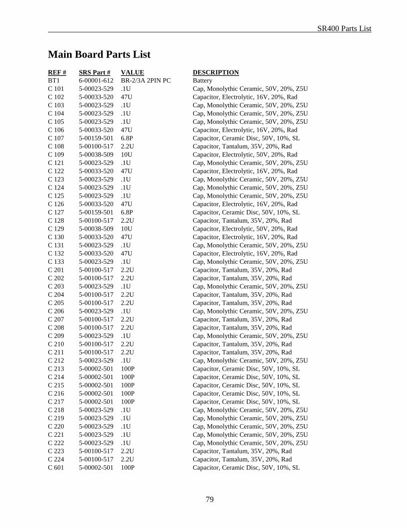
SR400 Parts List
79
Main Board Parts List REF # SRS Part # VALUE DESCRIPTION BT1 6-00001-612 BR-2/3A 2PIN PC Battery C 101 5-00023-529 .1U Cap, Monolythic Ceramic, 50V, 20%, Z5U C 102 5-00033-520 47U Capacitor, Electrolytic, 16V, 20%, Rad C 103 5-00023-529 .1U Cap, Monolythic Ceramic, 50V, 20%, Z5U C 104 5-00023-529 .1U Cap, Monolythic Ceramic, 50V, 20%, Z5U C 105 5-00023-529 .1U Cap, Monolythic Ceramic, 50V, 20%, Z5U C 106 5-00033-520 47U Capacitor, Electrolytic, 16V, 20%, Rad C 107 5-00159-501 6.8P Capacitor, Ceramic Disc, 50V, 10%, SL C 108 5-00100-517 2.2U Capacitor, Tantalum, 35V, 20%, Rad C 109 5-00038-509 10U Capacitor, Electrolytic, 50V, 20%, Rad C 121 5-00023-529 .1U Cap, Monolythic Ceramic, 50V, 20%, Z5U C 122 5-00033-520 47U Capacitor, Electrolytic, 16V, 20%, Rad C 123 5-00023-529 .1U Cap, Monolythic Ceramic, 50V, 20%, Z5U C 124 5-00023-529 .1U Cap, Monolythic Ceramic, 50V, 20%, Z5U C 125 5-00023-529 .1U Cap, Monolythic Ceramic, 50V, 20%, Z5U C 126 5-00033-520 47U Capacitor, Electrolytic, 16V, 20%, Rad C 127 5-00159-501 6.8P Capacitor, Ceramic Disc, 50V, 10%, SL C 128 5-00100-517 2.2U Capacitor, Tantalum, 35V, 20%, Rad C 129 5-00038-509 10U Capacitor, Electrolytic, 50V, 20%, Rad C 130 5-00033-520 47U Capacitor, Electrolytic, 16V, 20%, Rad C 131 5-00023-529 .1U Cap, Monolythic Ceramic, 50V, 20%, Z5U C 132 5-00033-520 47U Capacitor, Electrolytic, 16V, 20%, Rad C 133 5-00023-529 .1U Cap, Monolythic Ceramic, 50V, 20%, Z5U C 201 5-00100-517 2.2U Capacitor, Tantalum, 35V, 20%, Rad C 202 5-00100-517 2.2U Capacitor, Tantalum, 35V, 20%, Rad C 203 5-00023-529 .1U Cap, Monolythic Ceramic, 50V, 20%, Z5U C 204 5-00100-517 2.2U Capacitor, Tantalum, 35V, 20%, Rad C 205 5-00100-517 2.2U Capacitor, Tantalum, 35V, 20%, Rad C 206 5-00023-529 .1U Cap, Monolythic Ceramic, 50V, 20%, Z5U C 207 5-00100-517 2.2U Capacitor, Tantalum, 35V, 20%, Rad C 208 5-00100-517 2.2U Capacitor, Tantalum, 35V, 20%, Rad C 209 5-00023-529 .1U Cap, Monolythic Ceramic, 50V, 20%, Z5U C 210 5-00100-517 2.2U Capacitor, Tantalum, 35V, 20%, Rad C 211 5-00100-517 2.2U Capacitor, Tantalum, 35V, 20%, Rad C 212 5-00023-529 .1U Cap, Monolythic Ceramic, 50V, 20%, Z5U C 213 5-00002-501 100P Capacitor, Ceramic Disc, 50V, 10%, SL C 214 5-00002-501 100P Capacitor, Ceramic Disc, 50V, 10%, SL C 215 5-00002-501 100P Capacitor, Ceramic Disc, 50V, 10%, SL C 216 5-00002-501 100P Capacitor, Ceramic Disc, 50V, 10%, SL C 217 5-00002-501 100P Capacitor, Ceramic Disc, 50V, 10%, SL C 218 5-00023-529 .1U Cap, Monolythic Ceramic, 50V, 20%, Z5U C 219 5-00023-529 .1U Cap, Monolythic Ceramic, 50V, 20%, Z5U C 220 5-00023-529 .1U Cap, Monolythic Ceramic, 50V, 20%, Z5U C 221 5-00023-529 .1U Cap, Monolythic Ceramic, 50V, 20%, Z5U C 222 5-00023-529 .1U Cap, Monolythic Ceramic, 50V, 20%, Z5U C 223 5-00100-517 2.2U Capacitor, Tantalum, 35V, 20%, Rad C 224 5-00100-517 2.2U Capacitor, Tantalum, 35V, 20%, Rad C 601 5-00002-501 100P Capacitor, Ceramic Disc, 50V, 10%, SL
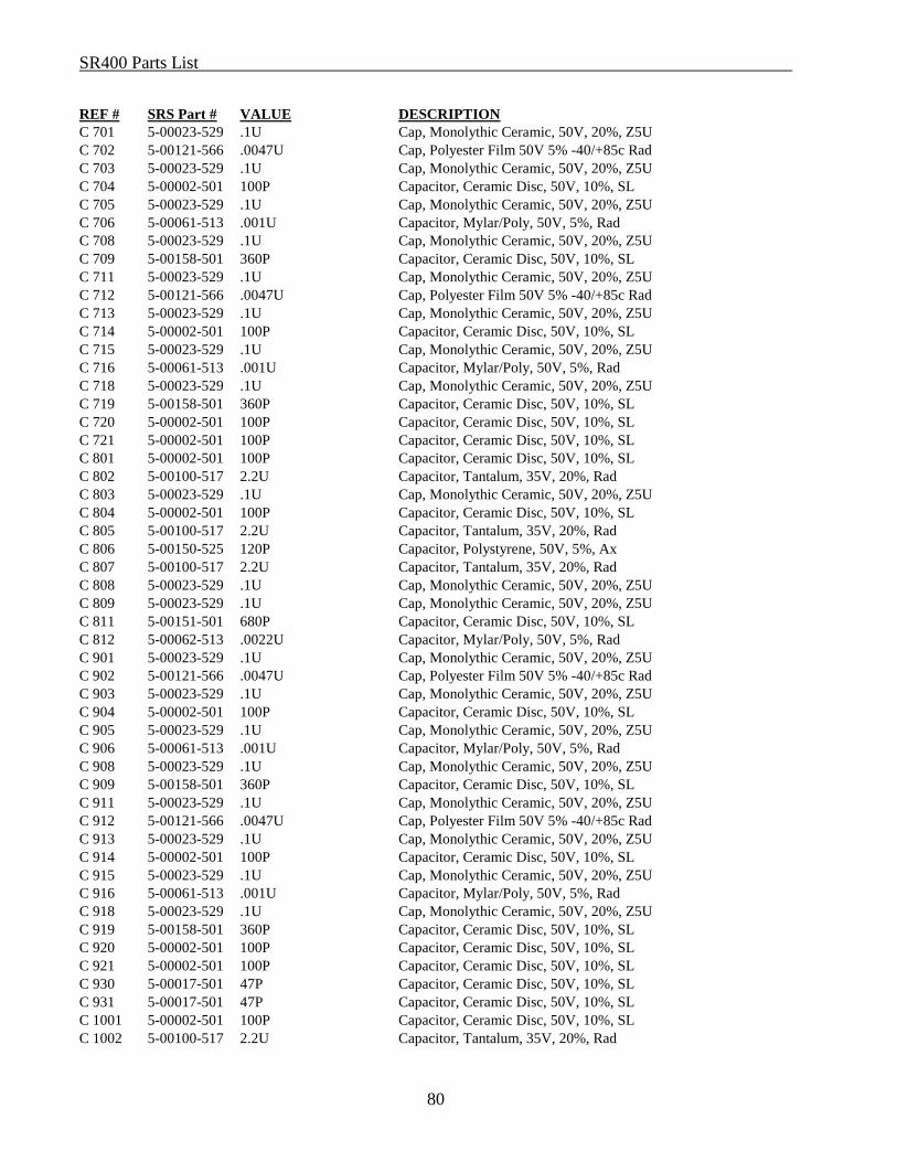
SR400 Parts List
80
REF # SRS Part # VALUE DESCRIPTION C 701 5-00023-529 .1U Cap, Monolythic Ceramic, 50V, 20%, Z5U C 702 5-00121-566 .0047U Cap, Polyester Film 50V 5% -40/+85c Rad C 703 5-00023-529 .1U Cap, Monolythic Ceramic, 50V, 20%, Z5U C 704 5-00002-501 100P Capacitor, Ceramic Disc, 50V, 10%, SL C 705 5-00023-529 .1U Cap, Monolythic Ceramic, 50V, 20%, Z5U C 706 5-00061-513 .001U Capacitor, Mylar/Poly, 50V, 5%, Rad C 708 5-00023-529 .1U Cap, Monolythic Ceramic, 50V, 20%, Z5U C 709 5-00158-501 360P Capacitor, Ceramic Disc, 50V, 10%, SL C 711 5-00023-529 .1U Cap, Monolythic Ceramic, 50V, 20%, Z5U C 712 5-00121-566 .0047U Cap, Polyester Film 50V 5% -40/+85c Rad C 713 5-00023-529 .1U Cap, Monolythic Ceramic, 50V, 20%, Z5U C 714 5-00002-501 100P Capacitor, Ceramic Disc, 50V, 10%, SL C 715 5-00023-529 .1U Cap, Monolythic Ceramic, 50V, 20%, Z5U C 716 5-00061-513 .001U Capacitor, Mylar/Poly, 50V, 5%, Rad C 718 5-00023-529 .1U Cap, Monolythic Ceramic, 50V, 20%, Z5U C 719 5-00158-501 360P Capacitor, Ceramic Disc, 50V, 10%, SL C 720 5-00002-501 100P Capacitor, Ceramic Disc, 50V, 10%, SL C 721 5-00002-501 100P Capacitor, Ceramic Disc, 50V, 10%, SL C 801 5-00002-501 100P Capacitor, Ceramic Disc, 50V, 10%, SL C 802 5-00100-517 2.2U Capacitor, Tantalum, 35V, 20%, Rad C 803 5-00023-529 .1U Cap, Monolythic Ceramic, 50V, 20%, Z5U C 804 5-00002-501 100P Capacitor, Ceramic Disc, 50V, 10%, SL C 805 5-00100-517 2.2U Capacitor, Tantalum, 35V, 20%, Rad C 806 5-00150-525 120P Capacitor, Polystyrene, 50V, 5%, Ax C 807 5-00100-517 2.2U Capacitor, Tantalum, 35V, 20%, Rad C 808 5-00023-529 .1U Cap, Monolythic Ceramic, 50V, 20%, Z5U C 809 5-00023-529 .1U Cap, Monolythic Ceramic, 50V, 20%, Z5U C 811 5-00151-501 680P Capacitor, Ceramic Disc, 50V, 10%, SL C 812 5-00062-513 .0022U Capacitor, Mylar/Poly, 50V, 5%, Rad C 901 5-00023-529 .1U Cap, Monolythic Ceramic, 50V, 20%, Z5U C 902 5-00121-566 .0047U Cap, Polyester Film 50V 5% -40/+85c Rad C 903 5-00023-529 .1U Cap, Monolythic Ceramic, 50V, 20%, Z5U C 904 5-00002-501 100P Capacitor, Ceramic Disc, 50V, 10%, SL C 905 5-00023-529 .1U Cap, Monolythic Ceramic, 50V, 20%, Z5U C 906 5-00061-513 .001U Capacitor, Mylar/Poly, 50V, 5%, Rad C 908 5-00023-529 .1U Cap, Monolythic Ceramic, 50V, 20%, Z5U C 909 5-00158-501 360P Capacitor, Ceramic Disc, 50V, 10%, SL C 911 5-00023-529 .1U Cap, Monolythic Ceramic, 50V, 20%, Z5U C 912 5-00121-566 .0047U Cap, Polyester Film 50V 5% -40/+85c Rad C 913 5-00023-529 .1U Cap, Monolythic Ceramic, 50V, 20%, Z5U C 914 5-00002-501 100P Capacitor, Ceramic Disc, 50V, 10%, SL C 915 5-00023-529 .1U Cap, Monolythic Ceramic, 50V, 20%, Z5U C 916 5-00061-513 .001U Capacitor, Mylar/Poly, 50V, 5%, Rad C 918 5-00023-529 .1U Cap, Monolythic Ceramic, 50V, 20%, Z5U C 919 5-00158-501 360P Capacitor, Ceramic Disc, 50V, 10%, SL C 920 5-00002-501 100P Capacitor, Ceramic Disc, 50V, 10%, SL C 921 5-00002-501 100P Capacitor, Ceramic Disc, 50V, 10%, SL C 930 5-00017-501 47P Capacitor, Ceramic Disc, 50V, 10%, SL C 931 5-00017-501 47P Capacitor, Ceramic Disc, 50V, 10%, SL C 1001 5-00002-501 100P Capacitor, Ceramic Disc, 50V, 10%, SL C 1002 5-00100-517 2.2U Capacitor, Tantalum, 35V, 20%, Rad
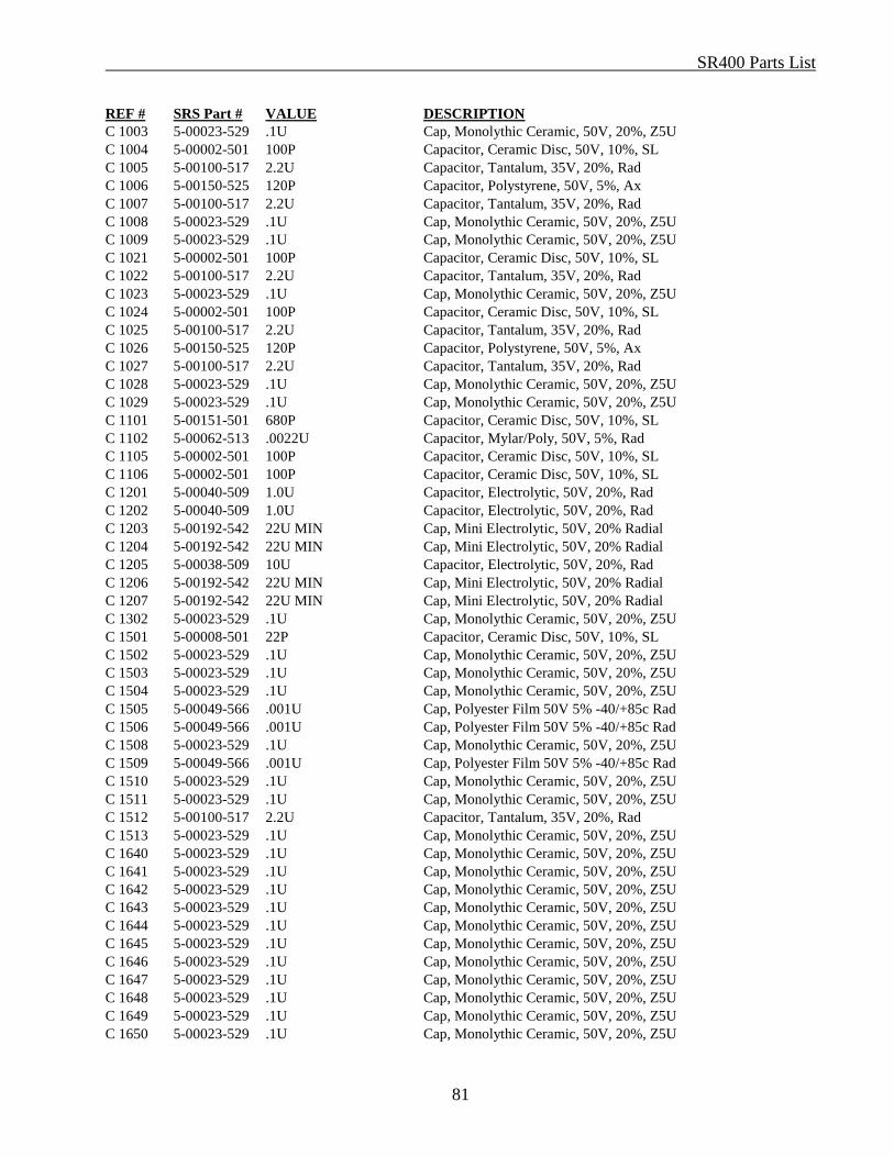
SR400 Parts List
81
REF # SRS Part # VALUE DESCRIPTION C 1003 5-00023-529 .1U Cap, Monolythic Ceramic, 50V, 20%, Z5U C 1004 5-00002-501 100P Capacitor, Ceramic Disc, 50V, 10%, SL C 1005 5-00100-517 2.2U Capacitor, Tantalum, 35V, 20%, Rad C 1006 5-00150-525 120P Capacitor, Polystyrene, 50V, 5%, Ax C 1007 5-00100-517 2.2U Capacitor, Tantalum, 35V, 20%, Rad C 1008 5-00023-529 .1U Cap, Monolythic Ceramic, 50V, 20%, Z5U C 1009 5-00023-529 .1U Cap, Monolythic Ceramic, 50V, 20%, Z5U C 1021 5-00002-501 100P Capacitor, Ceramic Disc, 50V, 10%, SL C 1022 5-00100-517 2.2U Capacitor, Tantalum, 35V, 20%, Rad C 1023 5-00023-529 .1U Cap, Monolythic Ceramic, 50V, 20%, Z5U C 1024 5-00002-501 100P Capacitor, Ceramic Disc, 50V, 10%, SL C 1025 5-00100-517 2.2U Capacitor, Tantalum, 35V, 20%, Rad C 1026 5-00150-525 120P Capacitor, Polystyrene, 50V, 5%, Ax C 1027 5-00100-517 2.2U Capacitor, Tantalum, 35V, 20%, Rad C 1028 5-00023-529 .1U Cap, Monolythic Ceramic, 50V, 20%, Z5U C 1029 5-00023-529 .1U Cap, Monolythic Ceramic, 50V, 20%, Z5U C 1101 5-00151-501 680P Capacitor, Ceramic Disc, 50V, 10%, SL C 1102 5-00062-513 .0022U Capacitor, Mylar/Poly, 50V, 5%, Rad C 1105 5-00002-501 100P Capacitor, Ceramic Disc, 50V, 10%, SL C 1106 5-00002-501 100P Capacitor, Ceramic Disc, 50V, 10%, SL C 1201 5-00040-509 1.0U Capacitor, Electrolytic, 50V, 20%, Rad C 1202 5-00040-509 1.0U Capacitor, Electrolytic, 50V, 20%, Rad C 1203 5-00192-542 22U MIN Cap, Mini Electrolytic, 50V, 20% Radial C 1204 5-00192-542 22U MIN Cap, Mini Electrolytic, 50V, 20% Radial C 1205 5-00038-509 10U Capacitor, Electrolytic, 50V, 20%, Rad C 1206 5-00192-542 22U MIN Cap, Mini Electrolytic, 50V, 20% Radial C 1207 5-00192-542 22U MIN Cap, Mini Electrolytic, 50V, 20% Radial C 1302 5-00023-529 .1U Cap, Monolythic Ceramic, 50V, 20%, Z5U C 1501 5-00008-501 22P Capacitor, Ceramic Disc, 50V, 10%, SL C 1502 5-00023-529 .1U Cap, Monolythic Ceramic, 50V, 20%, Z5U C 1503 5-00023-529 .1U Cap, Monolythic Ceramic, 50V, 20%, Z5U C 1504 5-00023-529 .1U Cap, Monolythic Ceramic, 50V, 20%, Z5U C 1505 5-00049-566 .001U Cap, Polyester Film 50V 5% -40/+85c Rad C 1506 5-00049-566 .001U Cap, Polyester Film 50V 5% -40/+85c Rad C 1508 5-00023-529 .1U Cap, Monolythic Ceramic, 50V, 20%, Z5U C 1509 5-00049-566 .001U Cap, Polyester Film 50V 5% -40/+85c Rad C 1510 5-00023-529 .1U Cap, Monolythic Ceramic, 50V, 20%, Z5U C 1511 5-00023-529 .1U Cap, Monolythic Ceramic, 50V, 20%, Z5U C 1512 5-00100-517 2.2U Capacitor, Tantalum, 35V, 20%, Rad C 1513 5-00023-529 .1U Cap, Monolythic Ceramic, 50V, 20%, Z5U C 1640 5-00023-529 .1U Cap, Monolythic Ceramic, 50V, 20%, Z5U C 1641 5-00023-529 .1U Cap, Monolythic Ceramic, 50V, 20%, Z5U C 1642 5-00023-529 .1U Cap, Monolythic Ceramic, 50V, 20%, Z5U C 1643 5-00023-529 .1U Cap, Monolythic Ceramic, 50V, 20%, Z5U C 1644 5-00023-529 .1U Cap, Monolythic Ceramic, 50V, 20%, Z5U C 1645 5-00023-529 .1U Cap, Monolythic Ceramic, 50V, 20%, Z5U C 1646 5-00023-529 .1U Cap, Monolythic Ceramic, 50V, 20%, Z5U C 1647 5-00023-529 .1U Cap, Monolythic Ceramic, 50V, 20%, Z5U C 1648 5-00023-529 .1U Cap, Monolythic Ceramic, 50V, 20%, Z5U C 1649 5-00023-529 .1U Cap, Monolythic Ceramic, 50V, 20%, Z5U C 1650 5-00023-529 .1U Cap, Monolythic Ceramic, 50V, 20%, Z5U
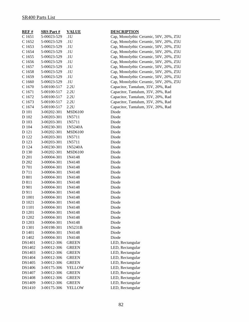
SR400 Parts List
82
REF # SRS Part # VALUE DESCRIPTION C 1651 5-00023-529 .1U Cap, Monolythic Ceramic, 50V, 20%, Z5U C 1652 5-00023-529 .1U Cap, Monolythic Ceramic, 50V, 20%, Z5U C 1653 5-00023-529 .1U Cap, Monolythic Ceramic, 50V, 20%, Z5U C 1654 5-00023-529 .1U Cap, Monolythic Ceramic, 50V, 20%, Z5U C 1655 5-00023-529 .1U Cap, Monolythic Ceramic, 50V, 20%, Z5U C 1656 5-00023-529 .1U Cap, Monolythic Ceramic, 50V, 20%, Z5U C 1657 5-00023-529 .1U Cap, Monolythic Ceramic, 50V, 20%, Z5U C 1658 5-00023-529 .1U Cap, Monolythic Ceramic, 50V, 20%, Z5U C 1659 5-00023-529 .1U Cap, Monolythic Ceramic, 50V, 20%, Z5U C 1660 5-00023-529 .1U Cap, Monolythic Ceramic, 50V, 20%, Z5U C 1670 5-00100-517 2.2U Capacitor, Tantalum, 35V, 20%, Rad C 1671 5-00100-517 2.2U Capacitor, Tantalum, 35V, 20%, Rad C 1672 5-00100-517 2.2U Capacitor, Tantalum, 35V, 20%, Rad C 1673 5-00100-517 2.2U Capacitor, Tantalum, 35V, 20%, Rad C 1674 5-00100-517 2.2U Capacitor, Tantalum, 35V, 20%, Rad D 101 3-00202-301 MSD6100 Diode D 102 3-00203-301 1N5711 Diode D 103 3-00203-301 1N5711 Diode D 104 3-00230-301 1N5240A Diode D 121 3-00202-301 MSD6100 Diode D 122 3-00203-301 1N5711 Diode D 123 3-00203-301 1N5711 Diode D 124 3-00230-301 1N5240A Diode D 130 3-00202-301 MSD6100 Diode D 201 3-00004-301 1N4148 Diode D 202 3-00004-301 1N4148 Diode D 701 3-00004-301 1N4148 Diode D 711 3-00004-301 1N4148 Diode D 801 3-00004-301 1N4148 Diode D 811 3-00004-301 1N4148 Diode D 901 3-00004-301 1N4148 Diode D 911 3-00004-301 1N4148 Diode D 1001 3-00004-301 1N4148 Diode D 1021 3-00004-301 1N4148 Diode D 1101 3-00004-301 1N4148 Diode D 1201 3-00004-301 1N4148 Diode D 1202 3-00004-301 1N4148 Diode D 1203 3-00004-301 1N4148 Diode D 1301 3-00198-301 1N5231B Diode D 1401 3-00004-301 1N4148 Diode D 1402 3-00004-301 1N4148 Diode DS1401 3-00012-306 GREEN LED, Rectangular DS1402 3-00012-306 GREEN LED, Rectangular DS1403 3-00012-306 GREEN LED, Rectangular DS1404 3-00012-306 GREEN LED, Rectangular DS1405 3-00012-306 GREEN LED, Rectangular DS1406 3-00175-306 YELLOW LED, Rectangular DS1407 3-00012-306 GREEN LED, Rectangular DS1408 3-00012-306 GREEN LED, Rectangular DS1409 3-00012-306 GREEN LED, Rectangular DS1410 3-00175-306 YELLOW LED, Rectangular
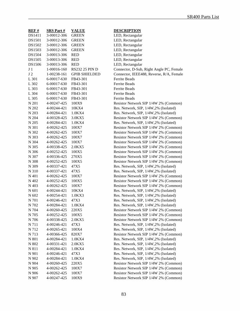
SR400 Parts List
83
REF # SRS Part # VALUE DESCRIPTION DS1411 3-00012-306 GREEN LED, Rectangular DS1501 3-00012-306 GREEN LED, Rectangular DS1502 3-00012-306 GREEN LED, Rectangular DS1503 3-00012-306 GREEN LED, Rectangular DS1504 3-00013-306 RED LED, Rectangular DS1505 3-00013-306 RED LED, Rectangular DS1506 3-00013-306 RED LED, Rectangular J 1 1-00016-160 RS232 25 PIN D Connector, D-Sub, Right Angle PC, Female J 2 1-00238-161 GPIB SHIELDED Connector, IEEE488, Reverse, R/A, Female L 301 6-00017-630 FB43-301 Ferrite Beads L 302 6-00017-630 FB43-301 Ferrite Beads L 303 6-00017-630 FB43-301 Ferrite Beads L 304 6-00017-630 FB43-301 Ferrite Beads L 305 6-00017-630 FB43-301 Ferrite Beads N 201 4-00247-425 100X9 Resistor Network SIP 1/4W 2% (Common) N 202 4-00244-421 10KX4 Res. Network, SIP, 1/4W,2% (Isolated) N 203 4-00284-421 1.0KX4 Res. Network, SIP, 1/4W,2% (Isolated) N 204 4-00328-425 3.0KX5 Resistor Network SIP 1/4W 2% (Common) N 205 4-00284-421 1.0KX4 Res. Network, SIP, 1/4W,2% (Isolated) N 301 4-00262-425 100X7 Resistor Network SIP 1/4W 2% (Common) N 302 4-00262-425 100X7 Resistor Network SIP 1/4W 2% (Common) N 303 4-00262-425 100X7 Resistor Network SIP 1/4W 2% (Common) N 304 4-00262-425 100X7 Resistor Network SIP 1/4W 2% (Common) N 305 4-00338-425 2.0KX5 Resistor Network SIP 1/4W 2% (Common) N 306 4-00252-425 100X5 Resistor Network SIP 1/4W 2% (Common) N 307 4-00336-425 270X5 Resistor Network SIP 1/4W 2% (Common) N 308 4-00252-425 100X5 Resistor Network SIP 1/4W 2% (Common) N 309 4-00337-421 47X5 Res. Network, SIP, 1/4W,2% (Isolated) N 310 4-00337-421 47X5 Res. Network, SIP, 1/4W,2% (Isolated) N 401 4-00262-425 100X7 Resistor Network SIP 1/4W 2% (Common) N 402 4-00252-425 100X5 Resistor Network SIP 1/4W 2% (Common) N 403 4-00262-425 100X7 Resistor Network SIP 1/4W 2% (Common) N 601 4-00244-421 10KX4 Res. Network, SIP, 1/4W,2% (Isolated) N 602 4-00254-421 1.0KX3 Res. Network, SIP, 1/4W,2% (Isolated) N 701 4-00246-421 47X3 Res. Network, SIP, 1/4W,2% (Isolated) N 702 4-00284-421 1.0KX4 Res. Network, SIP, 1/4W,2% (Isolated) N 704 4-00260-425 220X5 Resistor Network SIP 1/4W 2% (Common) N 705 4-00252-425 100X5 Resistor Network SIP 1/4W 2% (Common) N 706 4-00338-425 2.0KX5 Resistor Network SIP 1/4W 2% (Common) N 711 4-00246-421 47X3 Res. Network, SIP, 1/4W,2% (Isolated) N 712 4-00265-421 100X4 Res. Network, SIP, 1/4W,2% (Isolated) N 713 4-00366-425 820X7 Resistor Network SIP 1/4W 2% (Common) N 801 4-00284-421 1.0KX4 Res. Network, SIP, 1/4W,2% (Isolated) N 802 4-00331-421 2.0KX5 Res. Network, SIP, 1/4W,2% (Isolated) N 811 4-00284-421 1.0KX4 Res. Network, SIP, 1/4W,2% (Isolated) N 901 4-00246-421 47X3 Res. Network, SIP, 1/4W,2% (Isolated) N 902 4-00284-421 1.0KX4 Res. Network, SIP, 1/4W,2% (Isolated) N 904 4-00260-425 220X5 Resistor Network SIP 1/4W 2% (Common) N 905 4-00262-425 100X7 Resistor Network SIP 1/4W 2% (Common) N 906 4-00262-425 100X7 Resistor Network SIP 1/4W 2% (Common) N 907 4-00247-425 100X9 Resistor Network SIP 1/4W 2% (Common)
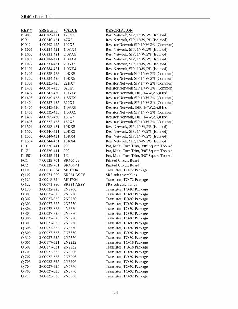
SR400 Parts List
84
REF # SRS Part # VALUE DESCRIPTION N 908 4-00369-421 120X3 Res. Network, SIP, 1/4W,2% (Isolated) N 911 4-00246-421 47X3 Res. Network, SIP, 1/4W,2% (Isolated) N 912 4-00262-425 100X7 Resistor Network SIP 1/4W 2% (Common) N 1001 4-00284-421 1.0KX4 Res. Network, SIP, 1/4W,2% (Isolated) N 1002 4-00331-421 2.0KX5 Res. Network, SIP, 1/4W,2% (Isolated) N 1021 4-00284-421 1.0KX4 Res. Network, SIP, 1/4W,2% (Isolated) N 1022 4-00331-421 2.0KX5 Res. Network, SIP, 1/4W,2% (Isolated) N 1101 4-00284-421 1.0KX4 Res. Network, SIP, 1/4W,2% (Isolated) N 1201 4-00335-425 20KX5 Resistor Network SIP 1/4W 2% (Common) N 1202 4-00334-425 10KX5 Resistor Network SIP 1/4W 2% (Common) N 1301 4-00223-425 22KX7 Resistor Network SIP 1/4W 2% (Common) N 1401 4-00287-425 820X9 Resistor Network SIP 1/4W 2% (Common) N 1402 4-00243-420 1.0KX8 Resistor Network, DIP, 1/4W,2%,8 Ind N 1403 4-00339-425 1.5KX9 Resistor Network SIP 1/4W 2% (Common) N 1404 4-00287-425 820X9 Resistor Network SIP 1/4W 2% (Common) N 1405 4-00243-420 1.0KX8 Resistor Network, DIP, 1/4W,2%,8 Ind N 1406 4-00339-425 1.5KX9 Resistor Network SIP 1/4W 2% (Common) N 1407 4-00365-420 150X7 Resistor Network, DIP, 1/4W,2%,8 Ind N 1408 4-00222-425 150X7 Resistor Network SIP 1/4W 2% (Common) N 1501 4-00333-421 10KX5 Res. Network, SIP, 1/4W,2% (Isolated) N 1502 4-00346-421 20KX5 Res. Network, SIP, 1/4W,2% (Isolated) N 1503 4-00244-421 10KX4 Res. Network, SIP, 1/4W,2% (Isolated) N 1504 4-00244-421 10KX4 Res. Network, SIP, 1/4W,2% (Isolated) P 101 4-00326-441 200 Pot, Multi-Turn Trim, 3/8" Square Top Ad P 121 4-00326-441 200 Pot, Multi-Turn Trim, 3/8" Square Top Ad P 1501 4-00485-441 1K Pot, Multi-Turn Trim, 3/8" Square Top Ad PC1 7-00125-701 SR400-29 Printed Circuit Board PC2 7-00129-701 SR400-41 Printed Circuit Board Q 101 3-00018-324 MRF904 Transistor, TO-72 Package Q 102 8-00071-860 SR534 ASSY SRS sub assemblies Q 121 3-00018-324 MRF904 Transistor, TO-72 Package Q 122 8-00071-860 SR534 ASSY SRS sub assemblies Q 130 3-00022-325 2N3906 Transistor, TO-92 Package Q 301 3-00027-325 2N5770 Transistor, TO-92 Package Q 302 3-00027-325 2N5770 Transistor, TO-92 Package Q 303 3-00027-325 2N5770 Transistor, TO-92 Package Q 304 3-00027-325 2N5770 Transistor, TO-92 Package Q 305 3-00027-325 2N5770 Transistor, TO-92 Package Q 306 3-00027-325 2N5770 Transistor, TO-92 Package Q 307 3-00027-325 2N5770 Transistor, TO-92 Package Q 308 3-00027-325 2N5770 Transistor, TO-92 Package Q 309 3-00027-325 2N5770 Transistor, TO-92 Package Q 310 3-00027-325 2N5770 Transistor, TO-92 Package Q 601 3-00177-321 2N2222 Transistor, TO-18 Package Q 602 3-00177-321 2N2222 Transistor, TO-18 Package Q 701 3-00022-325 2N3906 Transistor, TO-92 Package Q 702 3-00022-325 2N3906 Transistor, TO-92 Package Q 703 3-00022-325 2N3906 Transistor, TO-92 Package Q 704 3-00027-325 2N5770 Transistor, TO-92 Package Q 705 3-00027-325 2N5770 Transistor, TO-92 Package Q 711 3-00022-325 2N3906 Transistor, TO-92 Package
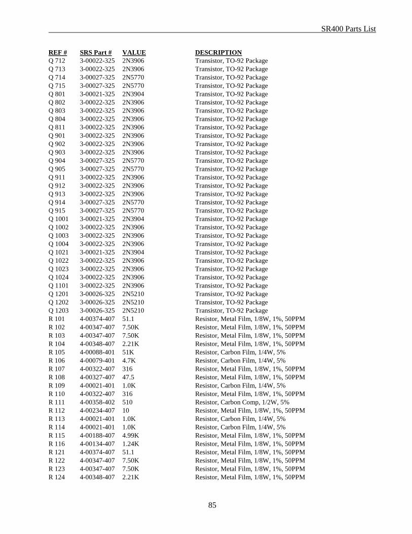
SR400 Parts List
85
REF # SRS Part # VALUE DESCRIPTION Q 712 3-00022-325 2N3906 Transistor, TO-92 Package Q 713 3-00022-325 2N3906 Transistor, TO-92 Package Q 714 3-00027-325 2N5770 Transistor, TO-92 Package Q 715 3-00027-325 2N5770 Transistor, TO-92 Package Q 801 3-00021-325 2N3904 Transistor, TO-92 Package Q 802 3-00022-325 2N3906 Transistor, TO-92 Package Q 803 3-00022-325 2N3906 Transistor, TO-92 Package Q 804 3-00022-325 2N3906 Transistor, TO-92 Package Q 811 3-00022-325 2N3906 Transistor, TO-92 Package Q 901 3-00022-325 2N3906 Transistor, TO-92 Package Q 902 3-00022-325 2N3906 Transistor, TO-92 Package Q 903 3-00022-325 2N3906 Transistor, TO-92 Package Q 904 3-00027-325 2N5770 Transistor, TO-92 Package Q 905 3-00027-325 2N5770 Transistor, TO-92 Package Q 911 3-00022-325 2N3906 Transistor, TO-92 Package Q 912 3-00022-325 2N3906 Transistor, TO-92 Package Q 913 3-00022-325 2N3906 Transistor, TO-92 Package Q 914 3-00027-325 2N5770 Transistor, TO-92 Package Q 915 3-00027-325 2N5770 Transistor, TO-92 Package Q 1001 3-00021-325 2N3904 Transistor, TO-92 Package Q 1002 3-00022-325 2N3906 Transistor, TO-92 Package Q 1003 3-00022-325 2N3906 Transistor, TO-92 Package Q 1004 3-00022-325 2N3906 Transistor, TO-92 Package Q 1021 3-00021-325 2N3904 Transistor, TO-92 Package Q 1022 3-00022-325 2N3906 Transistor, TO-92 Package Q 1023 3-00022-325 2N3906 Transistor, TO-92 Package Q 1024 3-00022-325 2N3906 Transistor, TO-92 Package Q 1101 3-00022-325 2N3906 Transistor, TO-92 Package Q 1201 3-00026-325 2N5210 Transistor, TO-92 Package Q 1202 3-00026-325 2N5210 Transistor, TO-92 Package Q 1203 3-00026-325 2N5210 Transistor, TO-92 Package R 101 4-00374-407 51.1 Resistor, Metal Film, 1/8W, 1%, 50PPM R 102 4-00347-407 7.50K Resistor, Metal Film, 1/8W, 1%, 50PPM R 103 4-00347-407 7.50K Resistor, Metal Film, 1/8W, 1%, 50PPM R 104 4-00348-407 2.21K Resistor, Metal Film, 1/8W, 1%, 50PPM R 105 4-00088-401 51K Resistor, Carbon Film, 1/4W, 5% R 106 4-00079-401 4.7K Resistor, Carbon Film, 1/4W, 5% R 107 4-00322-407 316 Resistor, Metal Film, 1/8W, 1%, 50PPM R 108 4-00327-407 47.5 Resistor, Metal Film, 1/8W, 1%, 50PPM R 109 4-00021-401 1.0K Resistor, Carbon Film, 1/4W, 5% R 110 4-00322-407 316 Resistor, Metal Film, 1/8W, 1%, 50PPM R 111 4-00358-402 510 Resistor, Carbon Comp, 1/2W, 5% R 112 4-00234-407 10 Resistor, Metal Film, 1/8W, 1%, 50PPM R 113 4-00021-401 1.0K Resistor, Carbon Film, 1/4W, 5% R 114 4-00021-401 1.0K Resistor, Carbon Film, 1/4W, 5% R 115 4-00188-407 4.99K Resistor, Metal Film, 1/8W, 1%, 50PPM R 116 4-00134-407 1.24K Resistor, Metal Film, 1/8W, 1%, 50PPM R 121 4-00374-407 51.1 Resistor, Metal Film, 1/8W, 1%, 50PPM R 122 4-00347-407 7.50K Resistor, Metal Film, 1/8W, 1%, 50PPM R 123 4-00347-407 7.50K Resistor, Metal Film, 1/8W, 1%, 50PPM R 124 4-00348-407 2.21K Resistor, Metal Film, 1/8W, 1%, 50PPM
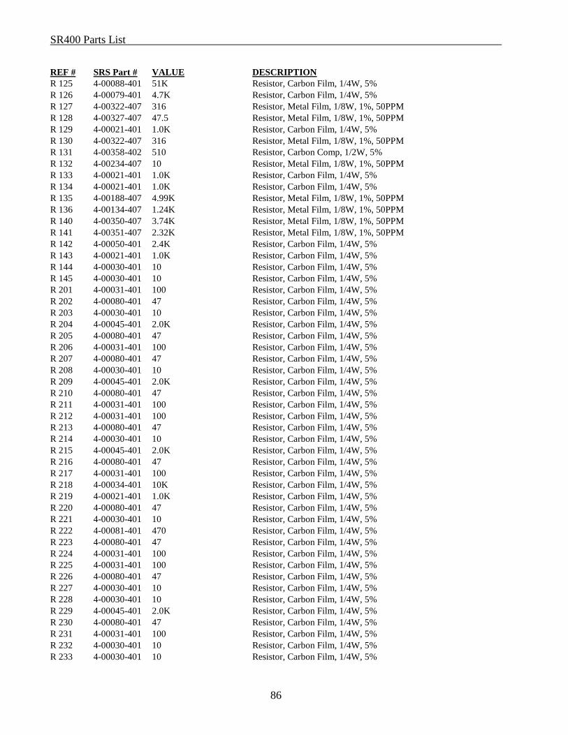
SR400 Parts List
86
REF # SRS Part # VALUE DESCRIPTION R 125 4-00088-401 51K Resistor, Carbon Film, 1/4W, 5% R 126 4-00079-401 4.7K Resistor, Carbon Film, 1/4W, 5% R 127 4-00322-407 316 Resistor, Metal Film, 1/8W, 1%, 50PPM R 128 4-00327-407 47.5 Resistor, Metal Film, 1/8W, 1%, 50PPM R 129 4-00021-401 1.0K Resistor, Carbon Film, 1/4W, 5% R 130 4-00322-407 316 Resistor, Metal Film, 1/8W, 1%, 50PPM R 131 4-00358-402 510 Resistor, Carbon Comp, 1/2W, 5% R 132 4-00234-407 10 Resistor, Metal Film, 1/8W, 1%, 50PPM R 133 4-00021-401 1.0K Resistor, Carbon Film, 1/4W, 5% R 134 4-00021-401 1.0K Resistor, Carbon Film, 1/4W, 5% R 135 4-00188-407 4.99K Resistor, Metal Film, 1/8W, 1%, 50PPM R 136 4-00134-407 1.24K Resistor, Metal Film, 1/8W, 1%, 50PPM R 140 4-00350-407 3.74K Resistor, Metal Film, 1/8W, 1%, 50PPM R 141 4-00351-407 2.32K Resistor, Metal Film, 1/8W, 1%, 50PPM R 142 4-00050-401 2.4K Resistor, Carbon Film, 1/4W, 5% R 143 4-00021-401 1.0K Resistor, Carbon Film, 1/4W, 5% R 144 4-00030-401 10 Resistor, Carbon Film, 1/4W, 5% R 145 4-00030-401 10 Resistor, Carbon Film, 1/4W, 5% R 201 4-00031-401 100 Resistor, Carbon Film, 1/4W, 5% R 202 4-00080-401 47 Resistor, Carbon Film, 1/4W, 5% R 203 4-00030-401 10 Resistor, Carbon Film, 1/4W, 5% R 204 4-00045-401 2.0K Resistor, Carbon Film, 1/4W, 5% R 205 4-00080-401 47 Resistor, Carbon Film, 1/4W, 5% R 206 4-00031-401 100 Resistor, Carbon Film, 1/4W, 5% R 207 4-00080-401 47 Resistor, Carbon Film, 1/4W, 5% R 208 4-00030-401 10 Resistor, Carbon Film, 1/4W, 5% R 209 4-00045-401 2.0K Resistor, Carbon Film, 1/4W, 5% R 210 4-00080-401 47 Resistor, Carbon Film, 1/4W, 5% R 211 4-00031-401 100 Resistor, Carbon Film, 1/4W, 5% R 212 4-00031-401 100 Resistor, Carbon Film, 1/4W, 5% R 213 4-00080-401 47 Resistor, Carbon Film, 1/4W, 5% R 214 4-00030-401 10 Resistor, Carbon Film, 1/4W, 5% R 215 4-00045-401 2.0K Resistor, Carbon Film, 1/4W, 5% R 216 4-00080-401 47 Resistor, Carbon Film, 1/4W, 5% R 217 4-00031-401 100 Resistor, Carbon Film, 1/4W, 5% R 218 4-00034-401 10K Resistor, Carbon Film, 1/4W, 5% R 219 4-00021-401 1.0K Resistor, Carbon Film, 1/4W, 5% R 220 4-00080-401 47 Resistor, Carbon Film, 1/4W, 5% R 221 4-00030-401 10 Resistor, Carbon Film, 1/4W, 5% R 222 4-00081-401 470 Resistor, Carbon Film, 1/4W, 5% R 223 4-00080-401 47 Resistor, Carbon Film, 1/4W, 5% R 224 4-00031-401 100 Resistor, Carbon Film, 1/4W, 5% R 225 4-00031-401 100 Resistor, Carbon Film, 1/4W, 5% R 226 4-00080-401 47 Resistor, Carbon Film, 1/4W, 5% R 227 4-00030-401 10 Resistor, Carbon Film, 1/4W, 5% R 228 4-00030-401 10 Resistor, Carbon Film, 1/4W, 5% R 229 4-00045-401 2.0K Resistor, Carbon Film, 1/4W, 5% R 230 4-00080-401 47 Resistor, Carbon Film, 1/4W, 5% R 231 4-00031-401 100 Resistor, Carbon Film, 1/4W, 5% R 232 4-00030-401 10 Resistor, Carbon Film, 1/4W, 5% R 233 4-00030-401 10 Resistor, Carbon Film, 1/4W, 5%
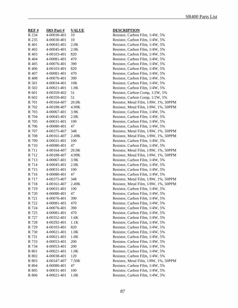
SR400 Parts List
87
REF # SRS Part # VALUE DESCRIPTION R 234 4-00030-401 10 Resistor, Carbon Film, 1/4W, 5% R 235 4-00030-401 10 Resistor, Carbon Film, 1/4W, 5% R 401 4-00045-401 2.0K Resistor, Carbon Film, 1/4W, 5% R 402 4-00045-401 2.0K Resistor, Carbon Film, 1/4W, 5% R 403 4-00103-401 820 Resistor, Carbon Film, 1/4W, 5% R 404 4-00081-401 470 Resistor, Carbon Film, 1/4W, 5% R 405 4-00076-401 390 Resistor, Carbon Film, 1/4W, 5% R 406 4-00103-401 820 Resistor, Carbon Film, 1/4W, 5% R 407 4-00081-401 470 Resistor, Carbon Film, 1/4W, 5% R 408 4-00076-401 390 Resistor, Carbon Film, 1/4W, 5% R 501 4-00034-401 10K Resistor, Carbon Film, 1/4W, 5% R 502 4-00021-401 1.0K Resistor, Carbon Film, 1/4W, 5% R 601 4-00359-402 51 Resistor, Carbon Comp, 1/2W, 5% R 602 4-00359-402 51 Resistor, Carbon Comp, 1/2W, 5% R 701 4-00164-407 20.0K Resistor, Metal Film, 1/8W, 1%, 50PPM R 702 4-00188-407 4.99K Resistor, Metal Film, 1/8W, 1%, 50PPM R 703 4-00067-401 3.9K Resistor, Carbon Film, 1/4W, 5% R 704 4-00045-401 2.0K Resistor, Carbon Film, 1/4W, 5% R 705 4-00031-401 100 Resistor, Carbon Film, 1/4W, 5% R 706 4-00080-401 47 Resistor, Carbon Film, 1/4W, 5% R 707 4-00375-407 348 Resistor, Metal Film, 1/8W, 1%, 50PPM R 708 4-00161-407 2.49K Resistor, Metal Film, 1/8W, 1%, 50PPM R 709 4-00031-401 100 Resistor, Carbon Film, 1/4W, 5% R 710 4-00080-401 47 Resistor, Carbon Film, 1/4W, 5% R 711 4-00164-407 20.0K Resistor, Metal Film, 1/8W, 1%, 50PPM R 712 4-00188-407 4.99K Resistor, Metal Film, 1/8W, 1%, 50PPM R 713 4-00067-401 3.9K Resistor, Carbon Film, 1/4W, 5% R 714 4-00045-401 2.0K Resistor, Carbon Film, 1/4W, 5% R 715 4-00031-401 100 Resistor, Carbon Film, 1/4W, 5% R 716 4-00080-401 47 Resistor, Carbon Film, 1/4W, 5% R 717 4-00375-407 348 Resistor, Metal Film, 1/8W, 1%, 50PPM R 718 4-00161-407 2.49K Resistor, Metal Film, 1/8W, 1%, 50PPM R 719 4-00031-401 100 Resistor, Carbon Film, 1/4W, 5% R 720 4-00080-401 47 Resistor, Carbon Film, 1/4W, 5% R 721 4-00076-401 390 Resistor, Carbon Film, 1/4W, 5% R 722 4-00081-401 470 Resistor, Carbon Film, 1/4W, 5% R 724 4-00076-401 390 Resistor, Carbon Film, 1/4W, 5% R 725 4-00081-401 470 Resistor, Carbon Film, 1/4W, 5% R 727 4-00352-401 1.6K Resistor, Carbon Film, 1/4W, 5% R 728 4-00292-401 1.1K Resistor, Carbon Film, 1/4W, 5% R 729 4-00103-401 820 Resistor, Carbon Film, 1/4W, 5% R 730 4-00021-401 1.0K Resistor, Carbon Film, 1/4W, 5% R 731 4-00021-401 1.0K Resistor, Carbon Film, 1/4W, 5% R 733 4-00053-401 200 Resistor, Carbon Film, 1/4W, 5% R 734 4-00053-401 200 Resistor, Carbon Film, 1/4W, 5% R 801 4-00021-401 1.0K Resistor, Carbon Film, 1/4W, 5% R 802 4-00038-401 120 Resistor, Carbon Film, 1/4W, 5% R 803 4-00347-407 7.50K Resistor, Metal Film, 1/8W, 1%, 50PPM R 804 4-00080-401 47 Resistor, Carbon Film, 1/4W, 5% R 805 4-00031-401 100 Resistor, Carbon Film, 1/4W, 5% R 806 4-00021-401 1.0K Resistor, Carbon Film, 1/4W, 5%

SR400 Parts List
88
REF # SRS Part # VALUE DESCRIPTION R 807 4-00305-401 4.3K Resistor, Carbon Film, 1/4W, 5% R 808 4-00021-401 1.0K Resistor, Carbon Film, 1/4W, 5% R 809 4-00305-401 4.3K Resistor, Carbon Film, 1/4W, 5% R 810 4-00215-407 909 Resistor, Metal Film, 1/8W, 1%, 50PPM R 811 4-00030-401 10 Resistor, Carbon Film, 1/4W, 5% R 812 4-00031-401 100 Resistor, Carbon Film, 1/4W, 5% R 901 4-00164-407 20.0K Resistor, Metal Film, 1/8W, 1%, 50PPM R 902 4-00188-407 4.99K Resistor, Metal Film, 1/8W, 1%, 50PPM R 903 4-00067-401 3.9K Resistor, Carbon Film, 1/4W, 5% R 904 4-00045-401 2.0K Resistor, Carbon Film, 1/4W, 5% R 905 4-00031-401 100 Resistor, Carbon Film, 1/4W, 5% R 906 4-00080-401 47 Resistor, Carbon Film, 1/4W, 5% R 907 4-00375-407 348 Resistor, Metal Film, 1/8W, 1%, 50PPM R 908 4-00161-407 2.49K Resistor, Metal Film, 1/8W, 1%, 50PPM R 909 4-00031-401 100 Resistor, Carbon Film, 1/4W, 5% R 910 4-00080-401 47 Resistor, Carbon Film, 1/4W, 5% R 911 4-00164-407 20.0K Resistor, Metal Film, 1/8W, 1%, 50PPM R 912 4-00188-407 4.99K Resistor, Metal Film, 1/8W, 1%, 50PPM R 913 4-00067-401 3.9K Resistor, Carbon Film, 1/4W, 5% R 914 4-00045-401 2.0K Resistor, Carbon Film, 1/4W, 5% R 915 4-00031-401 100 Resistor, Carbon Film, 1/4W, 5% R 916 4-00080-401 47 Resistor, Carbon Film, 1/4W, 5% R 917 4-00375-407 348 Resistor, Metal Film, 1/8W, 1%, 50PPM R 918 4-00161-407 2.49K Resistor, Metal Film, 1/8W, 1%, 50PPM R 919 4-00031-401 100 Resistor, Carbon Film, 1/4W, 5% R 920 4-00080-401 47 Resistor, Carbon Film, 1/4W, 5% R 921 4-00076-401 390 Resistor, Carbon Film, 1/4W, 5% R 922 4-00081-401 470 Resistor, Carbon Film, 1/4W, 5% R 924 4-00076-401 390 Resistor, Carbon Film, 1/4W, 5% R 925 4-00081-401 470 Resistor, Carbon Film, 1/4W, 5% R 927 4-00076-401 390 Resistor, Carbon Film, 1/4W, 5% R 928 4-00360-401 430 Resistor, Carbon Film, 1/4W, 5% R 930 4-00076-401 390 Resistor, Carbon Film, 1/4W, 5% R 931 4-00360-401 430 Resistor, Carbon Film, 1/4W, 5% R 940 4-00021-401 1.0K Resistor, Carbon Film, 1/4W, 5% R 941 4-00021-401 1.0K Resistor, Carbon Film, 1/4W, 5% R 942 4-00053-401 200 Resistor, Carbon Film, 1/4W, 5% R 943 4-00053-401 200 Resistor, Carbon Film, 1/4W, 5% R 1001 4-00021-401 1.0K Resistor, Carbon Film, 1/4W, 5% R 1002 4-00038-401 120 Resistor, Carbon Film, 1/4W, 5% R 1003 4-00347-407 7.50K Resistor, Metal Film, 1/8W, 1%, 50PPM R 1004 4-00080-401 47 Resistor, Carbon Film, 1/4W, 5% R 1005 4-00031-401 100 Resistor, Carbon Film, 1/4W, 5% R 1006 4-00021-401 1.0K Resistor, Carbon Film, 1/4W, 5% R 1007 4-00305-401 4.3K Resistor, Carbon Film, 1/4W, 5% R 1008 4-00021-401 1.0K Resistor, Carbon Film, 1/4W, 5% R 1009 4-00305-401 4.3K Resistor, Carbon Film, 1/4W, 5% R 1010 4-00215-407 909 Resistor, Metal Film, 1/8W, 1%, 50PPM R 1011 4-00030-401 10 Resistor, Carbon Film, 1/4W, 5% R 1012 4-00031-401 100 Resistor, Carbon Film, 1/4W, 5% R 1021 4-00021-401 1.0K Resistor, Carbon Film, 1/4W, 5%
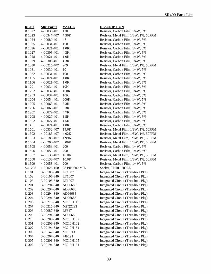
SR400 Parts List
89
REF # SRS Part # VALUE DESCRIPTION R 1022 4-00038-401 120 Resistor, Carbon Film, 1/4W, 5% R 1023 4-00347-407 7.50K Resistor, Metal Film, 1/8W, 1%, 50PPM R 1024 4-00080-401 47 Resistor, Carbon Film, 1/4W, 5% R 1025 4-00031-401 100 Resistor, Carbon Film, 1/4W, 5% R 1026 4-00021-401 1.0K Resistor, Carbon Film, 1/4W, 5% R 1027 4-00305-401 4.3K Resistor, Carbon Film, 1/4W, 5% R 1028 4-00021-401 1.0K Resistor, Carbon Film, 1/4W, 5% R 1029 4-00305-401 4.3K Resistor, Carbon Film, 1/4W, 5% R 1030 4-00215-407 909 Resistor, Metal Film, 1/8W, 1%, 50PPM R 1031 4-00030-401 10 Resistor, Carbon Film, 1/4W, 5% R 1032 4-00031-401 100 Resistor, Carbon Film, 1/4W, 5% R 1105 4-00021-401 1.0K Resistor, Carbon Film, 1/4W, 5% R 1106 4-00021-401 1.0K Resistor, Carbon Film, 1/4W, 5% R 1201 4-00034-401 10K Resistor, Carbon Film, 1/4W, 5% R 1202 4-00032-401 100K Resistor, Carbon Film, 1/4W, 5% R 1203 4-00034-401 10K Resistor, Carbon Film, 1/4W, 5% R 1204 4-00054-401 200K Resistor, Carbon Film, 1/4W, 5% R 1205 4-00065-401 3.3K Resistor, Carbon Film, 1/4W, 5% R 1206 4-00065-401 3.3K Resistor, Carbon Film, 1/4W, 5% R 1207 4-00079-401 4.7K Resistor, Carbon Film, 1/4W, 5% R 1208 4-00027-401 1.5K Resistor, Carbon Film, 1/4W, 5% R 1302 4-00027-401 1.5K Resistor, Carbon Film, 1/4W, 5% R 1401 4-00021-401 1.0K Resistor, Carbon Film, 1/4W, 5% R 1501 4-00332-407 19.6K Resistor, Metal Film, 1/8W, 1%, 50PPM R 1502 4-00185-407 4.02K Resistor, Metal Film, 1/8W, 1%, 50PPM R 1503 4-00188-407 4.99K Resistor, Metal Film, 1/8W, 1%, 50PPM R 1504 4-00206-407 8.06K Resistor, Metal Film, 1/8W, 1%, 50PPM R 1505 4-00053-401 200 Resistor, Carbon Film, 1/4W, 5% R 1506 4-00053-401 200 Resistor, Carbon Film, 1/4W, 5% R 1507 4-00138-407 10.0K Resistor, Metal Film, 1/8W, 1%, 50PPM R 1508 4-00138-407 10.0K Resistor, Metal Film, 1/8W, 1%, 50PPM R 1509 4-00053-401 200 Resistor, Carbon Film, 1/4W, 5% SO1208 1-00026-150 28 PIN 600 MIL Socket, THRU-HOLE U 101 3-00106-340 LT1007 Integrated Circuit (Thru-hole Pkg) U 102 3-00106-340 LT1007 Integrated Circuit (Thru-hole Pkg) U 103 3-00106-340 LT1007 Integrated Circuit (Thru-hole Pkg) U 201 3-00294-340 AD96685 Integrated Circuit (Thru-hole Pkg) U 202 3-00294-340 AD96685 Integrated Circuit (Thru-hole Pkg) U 203 3-00294-340 AD96685 Integrated Circuit (Thru-hole Pkg) U 204 3-00294-340 AD96685 Integrated Circuit (Thru-hole Pkg) U 206 3-00213-340 MC10H113 Integrated Circuit (Thru-hole Pkg) U 207 3-00215-340 MPQ2222 Integrated Circuit (Thru-hole Pkg) U 208 3-00087-340 LF347 Integrated Circuit (Thru-hole Pkg) U 209 3-00294-340 AD96685 Integrated Circuit (Thru-hole Pkg) U 210 3-00206-340 MC10H102 Integrated Circuit (Thru-hole Pkg) U 301 3-00206-340 MC10H102 Integrated Circuit (Thru-hole Pkg) U 302 3-00194-340 MC10H131 Integrated Circuit (Thru-hole Pkg) U 303 3-00142-340 MC10131 Integrated Circuit (Thru-hole Pkg) U 304 3-00207-340 74F191 Integrated Circuit (Thru-hole Pkg) U 305 3-00201-340 MC10H105 Integrated Circuit (Thru-hole Pkg) U 306 3-00194-340 MC10H131 Integrated Circuit (Thru-hole Pkg)
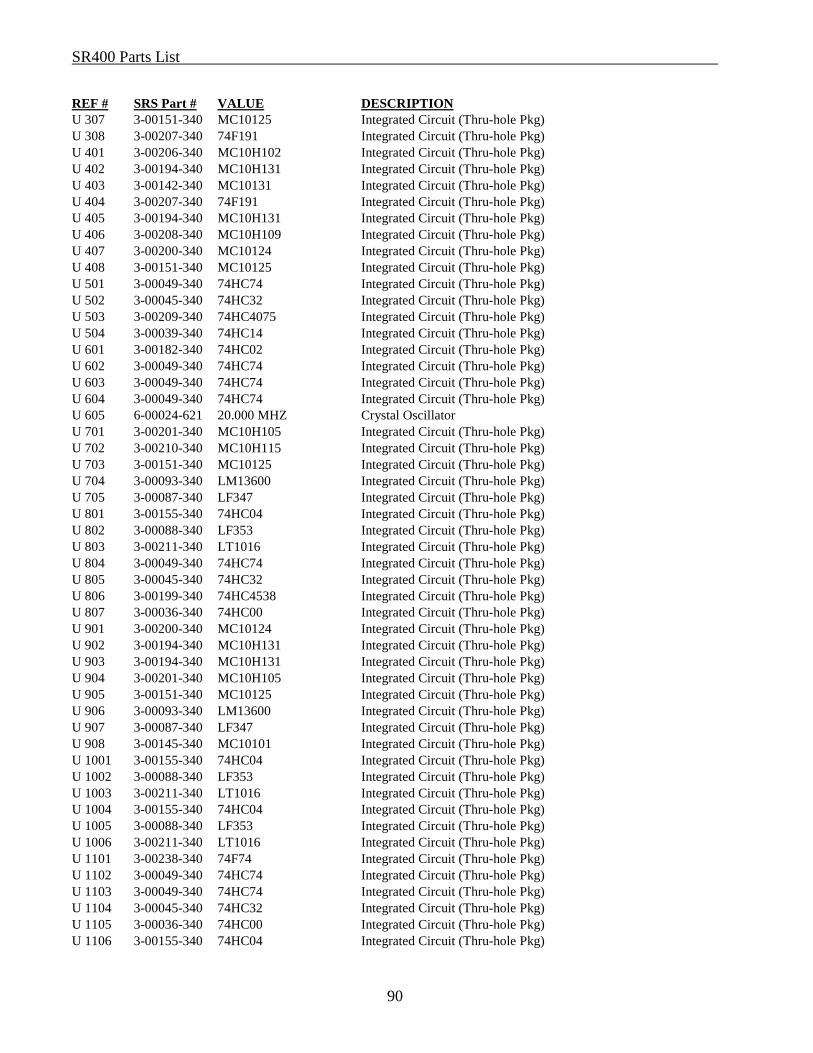
SR400 Parts List
90
REF # SRS Part # VALUE DESCRIPTION U 307 3-00151-340 MC10125 Integrated Circuit (Thru-hole Pkg) U 308 3-00207-340 74F191 Integrated Circuit (Thru-hole Pkg) U 401 3-00206-340 MC10H102 Integrated Circuit (Thru-hole Pkg) U 402 3-00194-340 MC10H131 Integrated Circuit (Thru-hole Pkg) U 403 3-00142-340 MC10131 Integrated Circuit (Thru-hole Pkg) U 404 3-00207-340 74F191 Integrated Circuit (Thru-hole Pkg) U 405 3-00194-340 MC10H131 Integrated Circuit (Thru-hole Pkg) U 406 3-00208-340 MC10H109 Integrated Circuit (Thru-hole Pkg) U 407 3-00200-340 MC10124 Integrated Circuit (Thru-hole Pkg) U 408 3-00151-340 MC10125 Integrated Circuit (Thru-hole Pkg) U 501 3-00049-340 74HC74 Integrated Circuit (Thru-hole Pkg) U 502 3-00045-340 74HC32 Integrated Circuit (Thru-hole Pkg) U 503 3-00209-340 74HC4075 Integrated Circuit (Thru-hole Pkg) U 504 3-00039-340 74HC14 Integrated Circuit (Thru-hole Pkg) U 601 3-00182-340 74HC02 Integrated Circuit (Thru-hole Pkg) U 602 3-00049-340 74HC74 Integrated Circuit (Thru-hole Pkg) U 603 3-00049-340 74HC74 Integrated Circuit (Thru-hole Pkg) U 604 3-00049-340 74HC74 Integrated Circuit (Thru-hole Pkg) U 605 6-00024-621 20.000 MHZ Crystal Oscillator U 701 3-00201-340 MC10H105 Integrated Circuit (Thru-hole Pkg) U 702 3-00210-340 MC10H115 Integrated Circuit (Thru-hole Pkg) U 703 3-00151-340 MC10125 Integrated Circuit (Thru-hole Pkg) U 704 3-00093-340 LM13600 Integrated Circuit (Thru-hole Pkg) U 705 3-00087-340 LF347 Integrated Circuit (Thru-hole Pkg) U 801 3-00155-340 74HC04 Integrated Circuit (Thru-hole Pkg) U 802 3-00088-340 LF353 Integrated Circuit (Thru-hole Pkg) U 803 3-00211-340 LT1016 Integrated Circuit (Thru-hole Pkg) U 804 3-00049-340 74HC74 Integrated Circuit (Thru-hole Pkg) U 805 3-00045-340 74HC32 Integrated Circuit (Thru-hole Pkg) U 806 3-00199-340 74HC4538 Integrated Circuit (Thru-hole Pkg) U 807 3-00036-340 74HC00 Integrated Circuit (Thru-hole Pkg) U 901 3-00200-340 MC10124 Integrated Circuit (Thru-hole Pkg) U 902 3-00194-340 MC10H131 Integrated Circuit (Thru-hole Pkg) U 903 3-00194-340 MC10H131 Integrated Circuit (Thru-hole Pkg) U 904 3-00201-340 MC10H105 Integrated Circuit (Thru-hole Pkg) U 905 3-00151-340 MC10125 Integrated Circuit (Thru-hole Pkg) U 906 3-00093-340 LM13600 Integrated Circuit (Thru-hole Pkg) U 907 3-00087-340 LF347 Integrated Circuit (Thru-hole Pkg) U 908 3-00145-340 MC10101 Integrated Circuit (Thru-hole Pkg) U 1001 3-00155-340 74HC04 Integrated Circuit (Thru-hole Pkg) U 1002 3-00088-340 LF353 Integrated Circuit (Thru-hole Pkg) U 1003 3-00211-340 LT1016 Integrated Circuit (Thru-hole Pkg) U 1004 3-00155-340 74HC04 Integrated Circuit (Thru-hole Pkg) U 1005 3-00088-340 LF353 Integrated Circuit (Thru-hole Pkg) U 1006 3-00211-340 LT1016 Integrated Circuit (Thru-hole Pkg) U 1101 3-00238-340 74F74 Integrated Circuit (Thru-hole Pkg) U 1102 3-00049-340 74HC74 Integrated Circuit (Thru-hole Pkg) U 1103 3-00049-340 74HC74 Integrated Circuit (Thru-hole Pkg) U 1104 3-00045-340 74HC32 Integrated Circuit (Thru-hole Pkg) U 1105 3-00036-340 74HC00 Integrated Circuit (Thru-hole Pkg) U 1106 3-00155-340 74HC04 Integrated Circuit (Thru-hole Pkg)
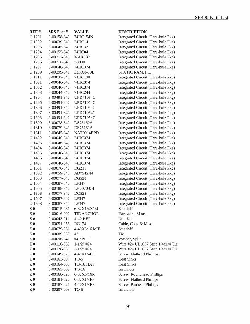
SR400 Parts List
91
REF # SRS Part # VALUE DESCRIPTION U 1201 3-00158-340 74HC154N Integrated Circuit (Thru-hole Pkg) U 1202 3-00039-340 74HC14 Integrated Circuit (Thru-hole Pkg) U 1203 3-00045-340 74HC32 Integrated Circuit (Thru-hole Pkg) U 1204 3-00155-340 74HC04 Integrated Circuit (Thru-hole Pkg) U 1205 3-00217-340 MAX232 Integrated Circuit (Thru-hole Pkg) U 1206 3-00216-340 Z8800 Integrated Circuit (Thru-hole Pkg) U 1207 3-00046-340 74HC374 Integrated Circuit (Thru-hole Pkg) U 1209 3-00299-341 32KX8-70L STATIC RAM, I.C. U 1211 3-00037-340 74HC138 Integrated Circuit (Thru-hole Pkg) U 1301 3-00046-340 74HC374 Integrated Circuit (Thru-hole Pkg) U 1302 3-00046-340 74HC374 Integrated Circuit (Thru-hole Pkg) U 1303 3-00044-340 74HC244 Integrated Circuit (Thru-hole Pkg) U 1304 3-00491-340 UPD71054C Integrated Circuit (Thru-hole Pkg) U 1305 3-00491-340 UPD71054C Integrated Circuit (Thru-hole Pkg) U 1306 3-00491-340 UPD71054C Integrated Circuit (Thru-hole Pkg) U 1307 3-00491-340 UPD71054C Integrated Circuit (Thru-hole Pkg) U 1308 3-00491-340 UPD71054C Integrated Circuit (Thru-hole Pkg) U 1309 3-00078-340 DS75160A Integrated Circuit (Thru-hole Pkg) U 1310 3-00079-340 DS75161A Integrated Circuit (Thru-hole Pkg) U 1311 3-00645-340 NAT9914BPD Integrated Circuit (Thru-hole Pkg) U 1402 3-00046-340 74HC374 Integrated Circuit (Thru-hole Pkg) U 1403 3-00046-340 74HC374 Integrated Circuit (Thru-hole Pkg) U 1404 3-00046-340 74HC374 Integrated Circuit (Thru-hole Pkg) U 1405 3-00046-340 74HC374 Integrated Circuit (Thru-hole Pkg) U 1406 3-00046-340 74HC374 Integrated Circuit (Thru-hole Pkg) U 1407 3-00046-340 74HC374 Integrated Circuit (Thru-hole Pkg) U 1501 3-00076-340 DG211 Integrated Circuit (Thru-hole Pkg) U 1502 3-00059-340 AD7542JN Integrated Circuit (Thru-hole Pkg) U 1503 3-00077-340 DG528 Integrated Circuit (Thru-hole Pkg) U 1504 3-00087-340 LF347 Integrated Circuit (Thru-hole Pkg) U 1505 3-00188-340 LH0070-0H Integrated Circuit (Thru-hole Pkg) U 1506 3-00077-340 DG528 Integrated Circuit (Thru-hole Pkg) U 1507 3-00087-340 LF347 Integrated Circuit (Thru-hole Pkg) U 1508 3-00087-340 LF347 Integrated Circuit (Thru-hole Pkg) Z 0 0-00015-031 6-32X1/4X1/4 Standoff Z 0 0-00016-000 TIE ANCHOR Hardware, Misc. Z 0 0-00043-011 4-40 KEP Nut, Kep Z 0 0-00051-056 RG174 Cable, Coax & Misc. Z 0 0-00079-031 4-40X3/16 M/F Standoff Z 0 0-00089-033 4" Tie Z 0 0-00096-041 #4 SPLIT Washer, Split Z 0 0-00110-053 1-1/2" #24 Wire #24 UL1007 Strip 1/4x1/4 Tin Z 0 0-00126-053 3-1/2" #24 Wire #24 UL1007 Strip 1/4x1/4 Tin Z 0 0-00149-020 4-40X1/4PF Screw, Flathead Phillips Z 0 0-00163-007 TO-5 Heat Sinks Z 0 0-00164-007 TO-18 HAT Heat Sinks Z 0 0-00165-003 TO-18 Insulators Z 0 0-00168-023 6-32X5/16R Screw, Roundhead Phillips Z 0 0-00181-020 6-32X1/4PF Screw, Flathead Phillips Z 0 0-00187-021 4-40X1/4PP Screw, Panhead Phillips Z 0 0-00207-003 TO-5 Insulators
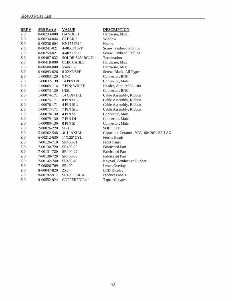
SR400 Parts List
92
REF # SRS Part # VALUE DESCRIPTION Z 0 0-00233-000 HANDLE1 Hardware, Misc. Z 0 0-00234-044 CLEAR 3 Window Z 0 0-00236-004 KN1751B1/4 Knobs Z 0 0-00241-021 4-40X3/16PP Screw, Panhead Phillips Z 0 0-00259-021 4-40X1/2"PP Screw, Panhead Phillips Z 0 0-00407-032 SOLDR SLV RG174 Termination Z 0 0-00418-000 CLIP, CABLE Hardware, Misc. Z 0 0-00500-000 554808-1 Hardware, Misc. Z 0 0-00893-026 8-32X3/8PF Screw, Black, All Types Z 0 1-00003-120 BNC Connector, BNC Z 0 1-00032-130 14 PIN DIL Connector, Male Z 0 1-00065-114 7 PIN; WHITE Header, Amp, MTA-100 Z 0 1-00073-120 INSL Connector, BNC Z 0 1-00074-171 14 CON DIL Cable Assembly, Ribbon Z 0 1-00075-171 8 PIN SIL Cable Assembly, Ribbon Z 0 1-00076-171 4 PIN SIL Cable Assembly, Ribbon Z 0 1-00077-171 7 PIN SIL Cable Assembly, Ribbon Z 0 1-00078-130 4 PIN SI Connector, Male Z 0 1-00079-130 7 PIN DI Connector, Male Z 0 1-00080-130 8 PIN SI Connector, Male Z 0 2-00026-220 SP-16 SOFTPOT Z 0 5-00262-548 .01U AXIAL Capacitor, Ceramic, 50V,+80/-20% Z5U AX Z 0 6-00212-630 1"X.25"CYL Ferrite Beads Z 0 7-00126-710 SR400-31 Front Panel Z 0 7-00130-720 SR400-20 Fabricated Part Z 0 7-00131-720 SR400-22 Fabricated Part Z 0 7-00138-720 SR400-39 Fabricated Part Z 0 7-00142-740 SR400-40 Keypad, Conductive Rubber Z 0 7-00826-709 SR400 Lexan Overlay Z 0 8-00047-820 2X24 LCD Display Z 0 9-00192-917 SR400 SERIAL Product Labels Z 0 9-00552-924 COPPERFOIL;1" Tape, All types
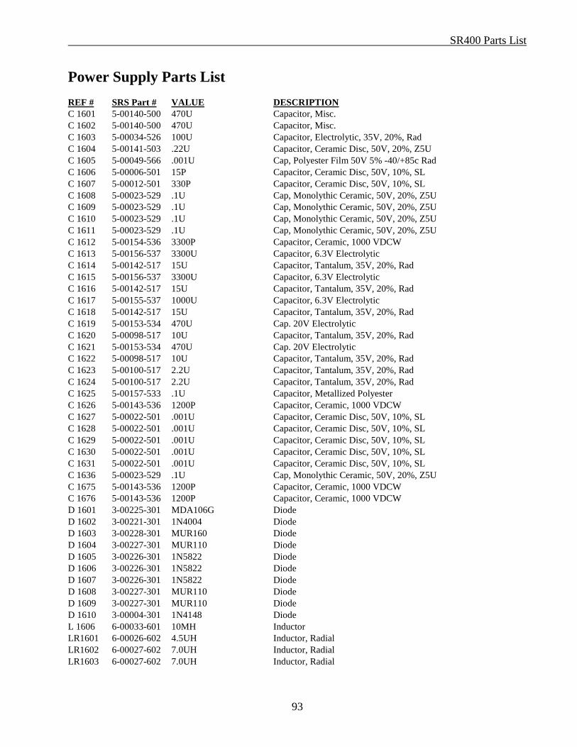
SR400 Parts List
93
Power Supply Parts List REF # SRS Part # VALUE DESCRIPTION C 1601 5-00140-500 470U Capacitor, Misc. C 1602 5-00140-500 470U Capacitor, Misc. C 1603 5-00034-526 100U Capacitor, Electrolytic, 35V, 20%, Rad C 1604 5-00141-503 .22U Capacitor, Ceramic Disc, 50V, 20%, Z5U C 1605 5-00049-566 .001U Cap, Polyester Film 50V 5% -40/+85c Rad C 1606 5-00006-501 15P Capacitor, Ceramic Disc, 50V, 10%, SL C 1607 5-00012-501 330P Capacitor, Ceramic Disc, 50V, 10%, SL C 1608 5-00023-529 .1U Cap, Monolythic Ceramic, 50V, 20%, Z5U C 1609 5-00023-529 .1U Cap, Monolythic Ceramic, 50V, 20%, Z5U C 1610 5-00023-529 .1U Cap, Monolythic Ceramic, 50V, 20%, Z5U C 1611 5-00023-529 .1U Cap, Monolythic Ceramic, 50V, 20%, Z5U C 1612 5-00154-536 3300P Capacitor, Ceramic, 1000 VDCW C 1613 5-00156-537 3300U Capacitor, 6.3V Electrolytic C 1614 5-00142-517 15U Capacitor, Tantalum, 35V, 20%, Rad C 1615 5-00156-537 3300U Capacitor, 6.3V Electrolytic C 1616 5-00142-517 15U Capacitor, Tantalum, 35V, 20%, Rad C 1617 5-00155-537 1000U Capacitor, 6.3V Electrolytic C 1618 5-00142-517 15U Capacitor, Tantalum, 35V, 20%, Rad C 1619 5-00153-534 470U Cap. 20V Electrolytic C 1620 5-00098-517 10U Capacitor, Tantalum, 35V, 20%, Rad C 1621 5-00153-534 470U Cap. 20V Electrolytic C 1622 5-00098-517 10U Capacitor, Tantalum, 35V, 20%, Rad C 1623 5-00100-517 2.2U Capacitor, Tantalum, 35V, 20%, Rad C 1624 5-00100-517 2.2U Capacitor, Tantalum, 35V, 20%, Rad C 1625 5-00157-533 .1U Capacitor, Metallized Polyester C 1626 5-00143-536 1200P Capacitor, Ceramic, 1000 VDCW C 1627 5-00022-501 .001U Capacitor, Ceramic Disc, 50V, 10%, SL C 1628 5-00022-501 .001U Capacitor, Ceramic Disc, 50V, 10%, SL C 1629 5-00022-501 .001U Capacitor, Ceramic Disc, 50V, 10%, SL C 1630 5-00022-501 .001U Capacitor, Ceramic Disc, 50V, 10%, SL C 1631 5-00022-501 .001U Capacitor, Ceramic Disc, 50V, 10%, SL C 1636 5-00023-529 .1U Cap, Monolythic Ceramic, 50V, 20%, Z5U C 1675 5-00143-536 1200P Capacitor, Ceramic, 1000 VDCW C 1676 5-00143-536 1200P Capacitor, Ceramic, 1000 VDCW D 1601 3-00225-301 MDA106G Diode D 1602 3-00221-301 1N4004 Diode D 1603 3-00228-301 MUR160 Diode D 1604 3-00227-301 MUR110 Diode D 1605 3-00226-301 1N5822 Diode D 1606 3-00226-301 1N5822 Diode D 1607 3-00226-301 1N5822 Diode D 1608 3-00227-301 MUR110 Diode D 1609 3-00227-301 MUR110 Diode D 1610 3-00004-301 1N4148 Diode L 1606 6-00033-601 10MH Inductor LR1601 6-00026-602 4.5UH Inductor, Radial LR1602 6-00027-602 7.0UH Inductor, Radial LR1603 6-00027-602 7.0UH Inductor, Radial
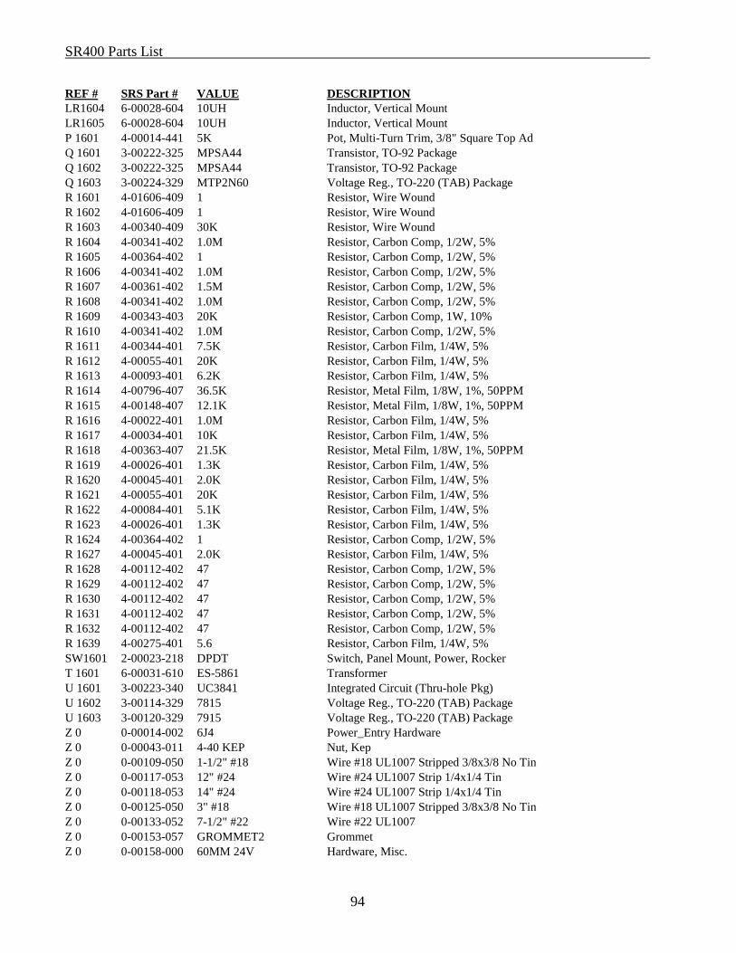
SR400 Parts List
94
REF # SRS Part # VALUE DESCRIPTION LR1604 6-00028-604 10UH Inductor, Vertical Mount LR1605 6-00028-604 10UH Inductor, Vertical Mount P 1601 4-00014-441 5K Pot, Multi-Turn Trim, 3/8" Square Top Ad Q 1601 3-00222-325 MPSA44 Transistor, TO-92 Package Q 1602 3-00222-325 MPSA44 Transistor, TO-92 Package Q 1603 3-00224-329 MTP2N60 Voltage Reg., TO-220 (TAB) Package R 1601 4-01606-409 1 Resistor, Wire Wound R 1602 4-01606-409 1 Resistor, Wire Wound R 1603 4-00340-409 30K Resistor, Wire Wound R 1604 4-00341-402 1.0M Resistor, Carbon Comp, 1/2W, 5% R 1605 4-00364-402 1 Resistor, Carbon Comp, 1/2W, 5% R 1606 4-00341-402 1.0M Resistor, Carbon Comp, 1/2W, 5% R 1607 4-00361-402 1.5M Resistor, Carbon Comp, 1/2W, 5% R 1608 4-00341-402 1.0M Resistor, Carbon Comp, 1/2W, 5% R 1609 4-00343-403 20K Resistor, Carbon Comp, 1W, 10% R 1610 4-00341-402 1.0M Resistor, Carbon Comp, 1/2W, 5% R 1611 4-00344-401 7.5K Resistor, Carbon Film, 1/4W, 5% R 1612 4-00055-401 20K Resistor, Carbon Film, 1/4W, 5% R 1613 4-00093-401 6.2K Resistor, Carbon Film, 1/4W, 5% R 1614 4-00796-407 36.5K Resistor, Metal Film, 1/8W, 1%, 50PPM R 1615 4-00148-407 12.1K Resistor, Metal Film, 1/8W, 1%, 50PPM R 1616 4-00022-401 1.0M Resistor, Carbon Film, 1/4W, 5% R 1617 4-00034-401 10K Resistor, Carbon Film, 1/4W, 5% R 1618 4-00363-407 21.5K Resistor, Metal Film, 1/8W, 1%, 50PPM R 1619 4-00026-401 1.3K Resistor, Carbon Film, 1/4W, 5% R 1620 4-00045-401 2.0K Resistor, Carbon Film, 1/4W, 5% R 1621 4-00055-401 20K Resistor, Carbon Film, 1/4W, 5% R 1622 4-00084-401 5.1K Resistor, Carbon Film, 1/4W, 5% R 1623 4-00026-401 1.3K Resistor, Carbon Film, 1/4W, 5% R 1624 4-00364-402 1 Resistor, Carbon Comp, 1/2W, 5% R 1627 4-00045-401 2.0K Resistor, Carbon Film, 1/4W, 5% R 1628 4-00112-402 47 Resistor, Carbon Comp, 1/2W, 5% R 1629 4-00112-402 47 Resistor, Carbon Comp, 1/2W, 5% R 1630 4-00112-402 47 Resistor, Carbon Comp, 1/2W, 5% R 1631 4-00112-402 47 Resistor, Carbon Comp, 1/2W, 5% R 1632 4-00112-402 47 Resistor, Carbon Comp, 1/2W, 5% R 1639 4-00275-401 5.6 Resistor, Carbon Film, 1/4W, 5% SW1601 2-00023-218 DPDT Switch, Panel Mount, Power, Rocker T 1601 6-00031-610 ES-5861 Transformer U 1601 3-00223-340 UC3841 Integrated Circuit (Thru-hole Pkg) U 1602 3-00114-329 7815 Voltage Reg., TO-220 (TAB) Package U 1603 3-00120-329 7915 Voltage Reg., TO-220 (TAB) Package Z 0 0-00014-002 6J4 Power_Entry Hardware Z 0 0-00043-011 4-40 KEP Nut, Kep Z 0 0-00109-050 1-1/2" #18 Wire #18 UL1007 Stripped 3/8x3/8 No Tin Z 0 0-00117-053 12" #24 Wire #24 UL1007 Strip 1/4x1/4 Tin Z 0 0-00118-053 14" #24 Wire #24 UL1007 Strip 1/4x1/4 Tin Z 0 0-00125-050 3" #18 Wire #18 UL1007 Stripped 3/8x3/8 No Tin Z 0 0-00133-052 7-1/2" #22 Wire #22 UL1007 Z 0 0-00153-057 GROMMET2 Grommet Z 0 0-00158-000 60MM 24V Hardware, Misc.

SR400 Parts List
95
REF # SRS Part # VALUE DESCRIPTION Z 0 0-00190-030 #8X1" Spacer Z 0 0-00200-043 #8 SHOULDER Washer, nylon Z 0 0-00208-020 4-40X3/8PF Screw, Flathead Phillips Z 0 0-00209-021 4-40X3/8PP Screw, Panhead Phillips Z 0 0-00231-043 #4 SHOULDER Washer, nylon Z 0 0-00243-003 TO-220 Insulators Z 0 0-00244-021 6-32X1-1/8PP Screw, Panhead Phillips Z 0 0-00438-021 4-40X5/16PP Screw, Panhead Phillips Z 0 0-00447-007 TO-220 Heat Sinks Z 0 0-00478-055 1.5"X#30 BLK Wire, Other Z 0 0-00523-048 5-5/8" #18 Wire, #18 UL1015 Strip 3/8 x 3/8 No Tin Z 0 1-00066-112 7 PIN; 24AWG/WH Connector, Amp, MTA-100 Z 0 6-00004-611 1A 3AG Fuse Z 0 7-00137-720 SR400-44 Fabricated Part Z 0 7-00139-720 SR400-27 Fabricated Part Z 0 7-00148-701 SR400 P/S Printed Circuit Board Z 0 9-00185-917 DANGER Product Labels
Miscellaneous and Chassis Assembly Parts List REF # SRS Part # VALUE DESCRIPTION U 1208 3-00229-342 27256-200 EPROM/PROM, I.C. Z 0 0-00098-042 #6 LOCK Washer, lock Z 0 0-00149-020 4-40X1/4PF Screw, Flathead Phillips Z 0 0-00167-023 6-32X1/2RP Screw, Roundhead Phillips Z 0 0-00179-000 RIGHT FOOT Hardware, Misc. Z 0 0-00180-000 LEFT FOOT Hardware, Misc. Z 0 0-00185-021 6-32X3/8PP Screw, Panhead Phillips Z 0 0-00204-000 REAR FOOT Hardware, Misc. Z 0 0-00237-016 F1404 Power Button Z 0 0-00238-026 6-32X1/4PF Screw, Black, All Types Z 0 0-00239-026 10-32X1/2PF Screw, Black, All Types Z 0 0-00240-026 4-40X3/8PF Screw, Black, All Types Z 0 7-00133-720 SR400-26 Fabricated Part Z 0 7-00134-720 SR400-23 Fabricated Part Z 0 7-00135-720 SR400-24 Fabricated Part Z 0 7-00140-720 SR400-37 Fabricated Part Z 0 7-00147-720 BAIL Fabricated Part

SR400 Parts List
96