modele standard eads astrium - european space...
TRANSCRIPT

TRP activity
Further Development of the Spacecraft Controller on a Chip
EXECUTIVE SUMMARY
EUROPEAN SPACE AGENCY CONTRACT REPORT
The work described in this report was done under ESA contract. Responsibility for the content resides in the author or the organisation that prepared it.
ESTEC Contract No. 20167/06/NL/FM
Prepared by : Franck KOEBEL
EADS Astrium
1, boulevard Jean Moulin
ZAC de la Clef Saint Pierre - CS 30503
78997 Elancourt Cedex
FRANCE

ESA STUDY CONTRACT REPORT
No ESA study Contract Report will be accepted unless this sheet is inserted at the beginning of each volume of the Report
* ESA Contract N°
20167/06/NL/FM
SUBJECT
Further Development of the Spacecraft
Controller on a Chip
Executive Summary
NAME OF CONTRACTOR
EADS Astrium
* ESA CR N°
* STAR CODE No of Volumes : 1
This is volume n°1
CONTRACTOR'S REFERENCE :
R&D.SCOC3.RP.01177.V.AS
TR
Issue 0 Rev 1
ABSTRACT:
The goal of the contract “Further Development of the Spacecraft Controller on a Chip” is to demonstrate the
feasibility, develop the methodology and IPs, and make the study of the SCOC3 ASIC up to the Logic Review
standard.
The work of the contract was necessary to assess and realize a very high integration level of functions coming
with the increasing demand of performance in terms of processing, power and mass.
Increasing amount of functionalities integrated into the same ASIC implies that the development of a whole
system relies on the use of pre-developed and pre-tested IP functions. The end target is to be able to construct
a whole system by “simply” integrating IP blocks. This often comes difficult and the alternative is still to rely on
modified IP blocks but very well tested and with a well-known history.
The requirements and functionalities of SCOC3 come from the SOW of the contract and a review of the
customer needs. It was then decided to implement a demonstrator of this SCOC3 into a commercial
reprogrammable FPGA, making the design available for a validation of the performances and functionalities by
HW or SW teams.
Gate level design methodology currently used for ASIC development has to be improved to focus on the
validation of the whole system design and take into account its greater complexity.
This work described in this report was done under ESA contract. Responsibility for the contents resides in author or organisation that prepared it.
Names of authors:
Franck KOEBEL (EADS Astrium)
ESA STUDY MANAGER
Mr Roland WEIGAND
DIV: TEC-EDM
ESA BUDGET HEADING
*Sectors to be completed by ESA

SCOC3 Ref : R&D.SCOC3.RP.01177.V.ASTR Issue : 0 Rev. : 1 Date : 02/02/2010 Page : 4
DOCUMENT CHANGE LOG
Issue/
Revision Date Modification Nb Modified pages Observations
0/0 26/06/09 First Issue 0/1 02/02/10 ESA comments
PAGE ISSUE RECORD Issue of this document comprises the following pages at the issue shown
Page Issue/ Rev.
Page Issue/ Rev.
Page Issue/ Rev.
Page Issue/ Rev.
Page Issue/ Rev.
Page Issue/ Rev.
all 0/1
SCOC3 Ref : R&D.SCOC3.RP.01177.V.ASTR Issue : 0 Rev. : 1 Date : 02/02/2010 Page : 5
TABLE OF CONTENTS
1 INTRODUCTION ..............................................................................................................................................6
1.1 CONTEXT AND RELEVANCE OF THE STUDY .......................................................................................................................... 6 1.2 ACRONYMS ................................................................................................................................................................................. 6
2 DESIGN OBJECTIVES AND CONSTRAINTS............................................................................................. 10
2.1 BACKGROUND.......................................................................................................................................................................... 10 2.2 DESIGN OBJECTIVES................................................................................................................................................................ 10
3 MAIN TOPICS .................................................................................................................................................. 12
3.1 SCOC3 ARCHITECTURE AND PERFORMANCES..................................................................................................................... 12 3.2 DISCUSSION ON THE IP CORES .............................................................................................................................................. 14
4 METHODOLOGY AND TOOLS.................................................................................................................... 18
4.1 METHODOLOGY ...................................................................................................................................................................... 18 4.2 TOOLS ........................................................................................................................................................................................ 20
5 EVOLUTION OF STUDY................................................................................................................................ 22
6 CONCLUSION.................................................................................................................................................. 22
LIST OF FIGURES
Figure 1 : SCOC3 overall architecture .....................................................................................................................13
Figure 2 : LEON3 processor core block diagram..................................................................................................15
Figure 3 : AHBR block diagram description...........................................................................................................15
Figure 4 : IPMON on AHB environment...............................................................................................................17
Figure 5 : Example of Write RMAP command list and reception ......................................................................17
Figure 6 : Spacewire assurance report sheet............................................................................................................19
Figure 7 : Overview of the SCOC3 testbench structure .......................................................................................19
Figure 8 : KerDive board ...........................................................................................................................................21
Figure 9 : Overview of the Modelsim simulation...................................................................................................21

SCOC3 Ref : R&D.SCOC3.RP.01177.V.ASTR Issue : 0 Rev. : 1 Date : 02/02/2010 Page : 6
1 INTRODUCTION
1.1 CONTEXT AND RELEVANCE OF THE STUDY
EADS Astrium has previously developed a SCOC prototype design along with an evaluation board (BLADE), as documented in Technical Documentation from Call-Off Order #3 (Spacecraft Controller On-a-Chip) of ESA contract #13345/99/NL/FM (Building Blocks for System On-a-Chip).
The interest of SCOC3 is to integrate most of the functions of an On Board Data Handling system, and to reduce significantly the cost of embedded electronics. The chip is named SCOC3 in the following document.
The present study is the continuation of the above mentioned “SCOC1” contract and EADS Astrium internal R&D activities (“SCOC2”). The aim of this activity is:
• to replace the LEON1 version used in the first contract by the LEON3,
• to improve the architecture in terms of performance,
• to develop new IPs that are missing and to validate them,
• to improve existing IPs and to verify them,
• to validate the SCOC3,
• to assess the gate level design phase by performing synthesis and static timing analysis on a selected technology.
A special attention has been paid to IP licensing problem in order to allow reuse and ASIC manufacturing.
1.2 ACRONYMS
Name Description AHB Advanced High-performance Bus AHBR AHb to ahb BRidge AMBA Advanced Microcontroller Bus Architecture AOCS Attitude and Orbital Control System APB Advanced Peripheral Bus ASIC Application Specific Integrated Circuit ASSP Application Specific Standard Product AUS AUthentication Status BC Bus Controller BCRT53 IP 1553 BC/RT/BM

SCOC3 Ref : R&D.SCOC3.RP.01177.V.ASTR Issue : 0 Rev. : 1 Date : 02/02/2010 Page : 7
BM Bus Monitor CAN Controller Area Network CCSDS Consultative Committee for Space Data Systems CLCW Command Link Control Word CPDU Command Pulse Distribution Unit CPDUS CPDU Status CPU Central Processing Unit CWP Current Window Pointer DMA Direct Memory Access DMATM DMA for TeleMetry DRAM Dynamic Random Access Memory DSU Debug Support Unit DSU3 Debug Support Unit for LEON3 EDAC Error Detection And Correction EEPROM Electronically Erasable Programmable Read Only Memory ESA European Space Agency FAR Frame Analysis Report FPGA Field Programmable Gate Array FPU Floating Point Unit GPS Global Positioning System GR Gaisler Research GRFPU Gaisler Research Floating Point Unit GRFPU-FT Gaisler Research Floating Point Unit Fault Tolerant GRLIB Gaisler Research LIBrary HADMA aHb Asynchronous Direct Memory Access HDL Hardware Description Language HK HouseKeePing HKPF HouseKeePing Function HW HardWare I/F Interface I/O Input/Output ICS Improved Channel Selection ICTL1 SCOC3 Primary Interrupt Controller ICTL2 SCOC3 Secondary Interrupt Controller IEEE Institute of Electrical & Electronics Engineers INRX Spacewire INTernal for Reception INST Instruction INTX Spacewire INTernal for Transmission IO Input / Output IOAHBCTL IO AHB Controller IP Intellectual Property IPL Inter Processor Link IPMON IP MONitor IRQ Interrupt ReQuest IRQMP Multi-Processor Interrupt ReQuest controller LEON (not an acronym) SPARC V8 32-bit processor LGPL Lesser General Public License LRU Least Recently Used LSB Least Significant Bit MACS Modular Attitude Contol System MAP Multiplexed Access Point MAPTCR MAP TC Recorder MISC MISCellaneous

SCOC3 Ref : R&D.SCOC3.RP.01177.V.ASTR Issue : 0 Rev. : 1 Date : 02/02/2010 Page : 8
MMU Memory Management Unit MPW Multi Project Wafer MSB Most Significant Bit NRZ Non Return to Zero OBC On Board Computer OBDH On-Board Data Handling PC Personal Computer PLL Phase Locked Loop PM Processor Module PROM Programmable Read Only Memory PTD Packet Telecommand Decoder PTME Packet TeleMetry Encoder QPSK Quaternary Phase Shift Keying R/W Readable/Writable RAM Random Access Memory RD Reference Document RHI RX Host Interface RMAP ReMote Access Protocol RMW Read Modify Write ROM Read Only Memory RS Reed Solomon RST ReSeT RT Remote Terminal RTL Register Transfer Language SA Sub Address (1553 context) SCET SpaceCraft Elapsed Time SCOC Spacecraft Controller On a Chip SCOC1 Spacecraft Controller On a Chip 1 (based on LEON1) SCOC3 Spacecraft Controller On a Chip 3 (based on LEON3-FT) SCTM SCOC3 CCSDS Time Manager SDRAM Synchronous Dynamic Random Access Memory SET Single Effect Transient SGM SafeGuard Memory SIF Service InterFace SIP System-In-Package SL Segment Layer SoC or SOC System-on-Chip SOFT SOFTware SPARC Scalable Processor ARChitecture SpW SpaceWire SpW-RMAP SpaceWire Remote Memory Access Protocol SRAM Static Random Access Memory STME SCOC3 PTME SW SoftWare SWMA SWitch MAtrix TAI International Atomic Time ("Temps Atomique International" in
French) TC TeleCommand TCDD TeleCommand Decoder Divas TCL Tool Command Language TCR TeleCommand Redundant module THI TX Host Interface TM Telemetry

SCOC3 Ref : R&D.SCOC3.RP.01177.V.ASTR Issue : 0 Rev. : 1 Date : 02/02/2010 Page : 9
TMTC TeleMetry and TeleCommand TT Trap Type UART Universal Asynchronous Receiver Transmitter USO Ultra Stable Oscillator USTM USer TeleMetry UTC Coordinated Universal Time VASI Very Advanced Sparc Interface (ERC32 Companion Chip) VCA Virtual Channel Access VCID Virtual Channel ID VCM Virtual Channel Multiplexer VHDL Very High Speed Integrated Circuit Hardware Description Language XSTR Cross-STRapping

SCOC3 Ref : R&D.SCOC3.RP.01177.V.ASTR Issue : 0 Rev. : 1 Date : 02/02/2010 Page : 10
2 DESIGN OBJECTIVES AND CONSTRAINTS
2.1 BACKGROUND
The telecommunication satellite constellation market and the small satellite market drive to dramatically decrease spacecraft equipment weight, consumption budget and recurrent price. The emerging micro satellites and nano satellites generation generates also a demand for much more integrated equipment. ESA and industrials developed in the years 80 and 90 sets of ASICs to reduce the size of electronics. Functions such as the VCA, VCM and PTD used to build a CCSDS TM/TC system, bus interfaces such as MACS, OBDH, 1553, or error correction chips (EDAC, Reed-Solomon, Viterbi…) were manufactured as Application Specific Standard Products (ASSP).
In the past years, the ASICs developed under ESA contracts were offered to European industrials as ASSP. Most of these chips were designed by using the VHDL language creating software macros that can be reused under certain conditions. The idea by now is to merge most of these available blocks in a single ASIC called “System-on-a-Chip” that would be able to perform a large number of the Data Management System functions of a platform.
The SCOC3 is the achievement of this approach for Space system, leading to the SIP (System In a Package) emerging concept. The SIP will also contain:
• memories (SDRAM, SRAM, EEPROM, Flash…)
• drivers (e.g. CAN, 1553…)
2.2 DESIGN OBJECTIVES
The system-on-a-chip approach is a necessary innovation for the European industry. It became feasible as the number of gates per ASIC had grown enough. There are at least two main domains of applications that require ASICs in Space, which are:
• The digital signal processing for which the available technologies are far from the requirement in terms of gate and in term of limitation of the power dissipation. These functions are by now far from the System-On-a-Chip concept since they integrate for some of them hundreds of ASICs.
• The Data Management Systems composed of elementary ASICs designed by the industrials or bought as ASSP after their development under an ESA contract. These functions can be integrated together with the microprocessor into a System-On-Chip to reduce power and mass budget.
By now Data Management Systems are built around a microprocessor, backplane bus interface, external serial bus interfaces, positioning functions such as GPS, TM/TC functions... The first contract has proven that it is possible to integrate most of these functions on a single die. The final objective of the SCOC series of activities is to produce an ASIC, available as off-the-shelf component to European Industry, which will simplify the architecture of future onboard control and data handling (OBDH) systems. The device functionality is comprehensive such as to satisfy a large variety of requirements, yet is scalable such as to be able to work in systems not using all of the features at reduced power consumption.

SCOC3 Ref : R&D.SCOC3.RP.01177.V.ASTR Issue : 0 Rev. : 1 Date : 02/02/2010 Page : 11
Earth observation and scientific satellite developers are candidates to use the SCOC3. Work has been performed in order to convince them that the reliability of an integrated solution is acceptable. Robust redundancy schemes have been proposed. The use of cache was a main concern for real time software developers. Most internal studies in this domain lead to a solution satisfying both hardware and software teams.
SCOC3 developed in this activity is a single chip Spacecraft Control System ASIC comprising the following functions:
• A LEON3-FT SPARC V8 processor including DSU for debug with GRFPU-FT floating point Unit and Memory Management Unit (MMU)
• 2 * 1553 BC/BM/RT controllers (each exclusive with the CAN controller that shares pins)
• 2 * CAN controllers (each exclusive with the 1553 controller that shares pins)
• A CCSDS TC decoder
• A CCSDS TM encoder
• An Housekeeping module
• A SCOC3 CCSDS Time Management controller (SCTM)
• 8 * SpaceWire controllers
• 4 * UART controllers
• 2 * memory controllers (One dedicated to CPU and one dedicated to IO)
• An AHB bus monitoring
• A MAPTCR with CONF
The goal of this activity is to have a verified RTL design which is ready to be mapped into an ASIC. The present activity includes the architecture definition of the component, the coding of its HDL model including IPs (existing, new and procured) and the verification by simulation and by prototyping at hardware level, and preliminary synthesis.
The activity covers the Specification and Architectural Design phases of the ASIC development according to ECSS-Q-60-02A.

SCOC3 Ref : R&D.SCOC3.RP.01177.V.ASTR Issue : 0 Rev. : 1 Date : 02/02/2010 Page : 12
3 MAIN TOPICS
3.1 SCOC3 ARCHITECTURE AND PERFORMANCES
The architecture of the SCOC3 is developed with modularity around validated blocks and new ones. This modularity is based on the internal bus structure and on standardized services provided to the blocks, like interrupts management and time distribution, independently of their intrinsic functionality.
Internal bus performances
The analysis of standard system requirements drives the SCOC3 bus architecture selection and leads to a choice of 2 AMBA AHB busses. The performances of this architecture for the targeted application have been evaluated and proven to be good. The hardware evaluation platform provided with the KerDive board is an excellent tool for architecture implementation and evaluation.
Data Transfer
The integration of complex IO interfaces within the same chip as the CPU needs a study of data exchanges mechanisms between the peripherals. In the SCOC3, DMA mechanisms have been distributed over each function. This allows having high and efficient transfer rates with a little use of the CPU.
SCOC3 Control
The SCOC3 is mainly controlled through the APB bus. All IP cores are connected to this bus for configuration and status register access. This structure allows the control of the SCOC3 by any AHB master connected to the CPU AHB bus. Basically the LEON3-FT CPU core acts as the main system controller, but the SCOC3 can also be configured by Spacewire thanks to RMAP protocol.
Time Management
The Time management and time distribution is not a specific issue of SCOC3. But SCOC3 has to anticipate the need of synchronisation between peripherals in its architecture, as the design is frozen in an ASIC. A synchronisation switch matrix is implemented into SCOC3 to adapt the function to specific system requirements.
Architecture confirmation
Based on the first contract and follow-up internal activities, the architecture of SCOC3 has been evaluated in terms of performances. Bottlenecks have been identified and taken into account for SCOC3 in hardware. Evolutions mainly consist in an upgrade of LEON CPU and a modification of the internal bus architecture to offer simultaneously higher performances in terms of computation and data transfer rates.

SCOC3 Ref : R&D.SCOC3.RP.01177.V.ASTR Issue : 0 Rev. : 1 Date : 02/02/2010 Page : 13
S
S
IP Monitor
SSPWINTTXDOSPWINTTXSO
SPWINTTXDISPWINTTXSI M
2TX
1NC
AN/T
X1N
BR
X1N
CAN
/RX1
NB
SpWIO
SPW
IOD
OSP
WIO
SOSP
WIO
DI
SPW
IOSI
UARTGP2
UARTGP1
TXG
P2R
XG
P2
TXG
P1R
XG
P1
M SSS
FPCTL
S
TX1R
/TX1
RB
RX1
R/R
X1R
B
TX1N
INH
TX1R
INH
2 2 2 2
BCRT53
PL
RX2
NC
AN/R
X2N
B
TX2R
/TX2
RB
RX2
R/R
X2R
B
TX2R
INH
2 2 2
TX2N
CAN
/TX2
NB
TX2N
INH
M MS S
CANPL
BCRT53
AV
CANAV
SS
CAN/1553 IF CAN/1553 IF
SpWSIFV
LEON3/GRFPU
MMInst/Data Cache
S
SPW
SIFD
OSP
WSI
FSO
SPW
SIFD
ISP
WSI
FSI
SPW
IPLD
OSP
WIP
LSO
S S M
APBRCPU
S S
SpWSIFO
S
SM
Timers
S S
AHBR
MM
HADMA
DSU CPU MCTL (SRAM,SDRAM)
CPU MEMORY
SS
DSU
BRE
DSU
ACT
DSU
EN
17
CD
ATA
CAD
D
48
AHBTraceBufferInst TraceBuffer
UART1
S
S
TXUA1RXUA1
SpWIPL
SPW
IPLD
ISP
WIP
LSI
CR
AMC
S0_N
CR
ASR
AMC
S1_N
CC
ASR
AMO
E_N
CW
ERAM
CS2
_NC
DQ
MAD
D18
CSD
RC
LKC
CKE
ADD
17
M
CPU APB
Fst IRQcontroller
S
GPIOsS 8GPIO
CR
AMW
E_N
CR
AMC
S3_N
CPU AHB BUS (arbiter, decoder)
UART DSU
STXUA2RXUA2
M
2nd IRQcontroller
S
CPU AHB STATUS
IO AHB BUS (arbiter, decoder)
IO MCTL (SRAM,SDRAM, PROMs)
IO functionalities
General
IO Count: 342
Gates Count: 1500 kgates
TCDD
SCOC3PTME
SCOC3Ccsds
TimeMng
Clock &Reset
SYSC
LKSY
SCLK
DIV
HW
RST
_N
TCC
LCW
CLK
TCC
LCW
SAM
PTC
CLC
WD
JTAG & SCAN
TRAN
S1TC
C/T
CS/
TCA
3 3 3
MAP
DAT
AO
8
M
S
MISC
CPU function
TM/TC function
Main clock/Other clock interface
IO M
EMO
RY:
(SG
M, B
OO
T, A
UTH
, EXC
H, M
M)
DMATM
TCR& CONF
OnChipMemTM
OnChipMemTC
HKPF
SwitchMatrix
S
S
S
S
MAP
ABTO
18
IODATAIOADD
48
IOCS_NIORASRAMCS1_NIOCASRAMOE_NIOWERAMCS2_NIODQMADD18IOSDRCLK
IOSGMPCS_N
IOPROMOE_N
IOATCPCS_N
IOPROMWE_N
MAP
CPD
UD
TRM
APC
PDU
DSR
TRAN
S2TC
C/T
CS/
TCA
TRAN
S3TC
C/T
CS/
TCA
MAP
TCO
DTR
MAP
TCO
DSR
MAP
DEC
OD
ATA
MAP
DEC
OC
LKM
APD
ECO
ABT
MAP
DEC
OD
TRM
APD
ECO
DSR
MAP
DEC
IDAT
AM
APD
ECIC
LKM
APD
ECID
TRM
APD
ECID
SR
PMID
LEIO
INH
IB
82
SYN
CSI
GG
PSN
/RR
TCLK
OR
TCLK
ITM
TIM
ESTR
IU
SOC
LK
CLK
16
TIM
EBAS
EOTI
ME
BASE
I
MAP
TCIC
LKM
APTC
IABT
MAP
TCID
TRM
APTC
IDSR
MAP
TCID
ATA
SpWUserTM
SPWUSTMDOSPWUSTMSO
SPWUSTMDISPWUSTMSI
SpWXStrping
SPWXSTRDOSPWXSTRSO
SPWXSTRDISPWXSTRSI
TMCLCWCLKTMCLCWSAMP
TMCLCWDTMTIMESTRO
TMIQCLKTMIOUT
TMQOUT
TMUECLKTMUEOUT
11
6
IOCKE1_2
BITC
LKI
S
S
M
M
M
M
S
S
VC0-
6VC
7-Id
le
Date: 2008/06/18
AU
EN
IOSWPCS_N6
IOBPCS_N
IOSWPEN
PMAL
IVE
IOBPENIOATCPEN
MAP
CPD
UC
LK
MAP
TCO
CLK
TRAN
S1R
FA
TRAN
S2R
FA
3
2
MAP
CPD
UD
ATA
DEC
STAS
PL
SS
S
APBRTMTC
M
TMTC APB
APBRIO
S
M
RST
_N
3
EXTI
T
2
IO APB
IO AHB STATUS
S
S
S
IOPROMDIRIOAREACS_N
IOCKE3_4IOCKE5_6IOCKE7_8IOCKE0_9IORAMWE_NIOCS0RAMCS0_NIOCS1RAMCS3_N
SpWIntRX
SPWINTRXDOSPWINTRXSO
SPWINTRXDISPWINTRXSI
S
MSP
WC
LKIN
SRAM
IOSE
LSR
AMC
PUS
EL
CKC
ON
F2C
KCO
NF1
TraceBufferStatsBuffer
SpWIntTX
Figure 1 : SCOC3 overall architecture
Two AHB busses, the CPU AHB for high performance, flow controlled interfaces, and the IO AHB for medium data rate interfaces, form the basics of the SCOC3 internal bus structure. LEON3-FT CPU is the main user on the CPU bus. The APB Busses allow accessing to all registers implemented in the different IP cores. Any master on the CPU AHB Bus can access to the APB busses as
Master through the APB Master interfaces. It is then possible to control the SCOC3 through the UART DSU interface for example. The hardware management of registers is split in three APB busses in order to separate different main functionalities such as processing,
peripherals and TM/TC.

SCOC3 Ref : R&D.SCOC3.RP.01177.V.ASTR Issue : 0 Rev. : 1 Date : 02/02/2010 Page : 14
3.2 DISCUSSION ON THE IP CORES
We can distinguish four main sources for the IP cores used within the Spacecraft Controller on a Chip 3: IP provided by ESA, commercial IPs, Astrium ASIC design modified as IP cores, and IP fully developed in the frame of this activity.
LEON3-FT: CPU core
LEON3-FT SPARC V8 core developed by Gaisler Research provides a powerful highly configurable CPU core available for integration within System on a Chip. It has many improvements since LEON1 since for instance this latter was not very well adapted to the use within a SoC, as LEON1 core can be seen itself as a SoC. Directly attached to the CPU is the GRFPU which is well adapted to fast floating point computations. There is also the possibility to use the MMU if needed. We choose to get a big cache size (2*64 KB) in order to improve performance as the technology allows big memories. It was noted however that this leads to a critical timing path in the LRU decoder.
SCTM: SCOC3 CCSDS Time Management
The SCTM provides all the functionalities for the on board CCSDS Time Management by integrating time keeping, alarms and pulse per second generation, event time tagging, time correlation and re-synchronisation. The SCTM is based on an ESA IP core, but an important work has been done on this IP to offer even more pulse generation frequencies in order to better fit to AOCS computation requirements.
STME: SCOC3 Packet Telemetry Encoder
The STME provides all the functionalities of the ground telemetry system, integrating the PTME IP from ESA. The functionalities have been wrapped into a single module including an internal memory buffer. Integration of PTME into SCOC3 has been performed without any major problem.
DMATM: DMA TeleMetry
To improve software management for STME, three DMA channels have been added in order to transfer Telemetry packets from the IO memory to the STME Virtual Channels. Several management modes are available including a dedicated status link with the Spacewire UserTM.
AHBR & HADMA: AHb to ahb BRidge & AHB Asynchronous Direct Memory Access
The AHBR & HADMA integrated into SCOC3 are the links between CPU and IO AHB busses.
Both allow using different clock frequencies on CPU AHB and IO AHB busses. They also manage different burst or access sizes. AHBR processes write accesses as posted writes. HADMA works like a usual DMA for its main function.
SCOC3 Ref : R&D.SCOC3.RP.01177.V.ASTR Issue : 0 Rev. : 1 Date : 02/02/2010 Page : 15
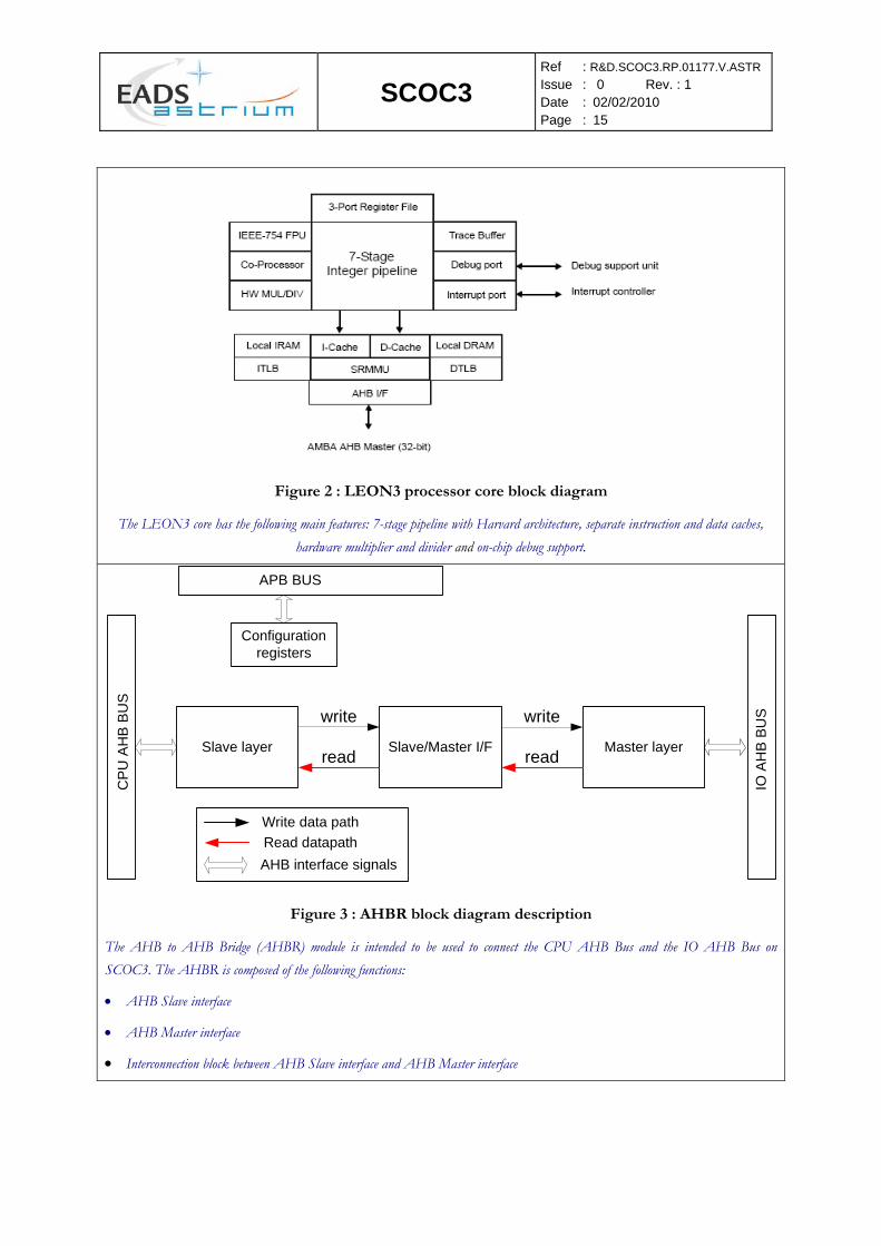
Figure 2 : LEON3 processor core block diagram
The LEON3 core has the following main features: 7-stage pipeline with Harvard architecture, separate instruction and data caches, hardware multiplier and divider and on-chip debug support.
Slave layer Master layerSlave/Master I/F
Write data pathRead datapathAHB interface signals
CP
U A
HB
BU
S
IO A
HB
BU
Swrite write
read read
APB BUS
Configurationregisters
Figure 3 : AHBR block diagram description
The AHB to AHB Bridge (AHBR) module is intended to be used to connect the CPU AHB Bus and the IO AHB Bus on SCOC3. The AHBR is composed of the following functions:
• AHB Slave interface
• AHB Master interface
• Interconnection block between AHB Slave interface and AHB Master interface

SCOC3 Ref : R&D.SCOC3.RP.01177.V.ASTR Issue : 0 Rev. : 1 Date : 02/02/2010 Page : 16
TCDD: Packet Telecommand Decoder
The TCDD is an improvement of the TC IP already implemented in SCOC1. The TC IP was derived from the well known PTD ASIC (MA28140). Work at segment layer level has been done in order to change MAP interfaces for CPDU, deciphering or cross-strapping purposes. All the four status registers FAR, CLCW, AUS, CPDUS can be read and written through APB. A local memory has been implemented in order to deal with authentication. This memory is scrubbed and protected by EDAC.
BCRT53: Mil-Std-1553 controller
The BCRT53 design is derived from the IP1553 used in VASI ASIC on EADS Astrium PM32 processor board. It integrates the Bus Controller, Remote Terminal and Bus Monitor capabilities on the Mil-Std-1553 bus. The BCRT53 design has been modified in order to get a synchronous reset to deal with SET sensitivity.
Spacewire-RMAP:
The Spacewire IP core allows achieving transfer rates at up to four times the system frequency. The IP was initially developed for SCOC1, and it was extended by an RMAP function for SCOC3. RMAP write command principle is given on Figure 5 as an example. The VHDL structure of the IP core clearly separates the Spacewire protocol management from the host interface. But including the RMAP function was more intrusive because it has to be done between the codec layer and the host interface. In order to limit interfaces and gate counts, we also simplified the host interface to have only one AHB master.
HKPF: House Keeping “Packetizer” function
The HKPF function automatically generates telemetry packets transferred to the virtual channel 6 of the STME. The telemetry sources are internal – telecommand report, time packet, context RAM dumping - for SCOC3.
IPMON: IP MONitor (Figure 4)
The IP Monitoring (IPMON) module is used to spy an AHB Bus, recording trace and statistics data. This IP is designed in the context of the SCOC3 project but can be used as a generic AHB spy module. It has sophisticated triggering conditions to trace the exchanges on the IO AHB bus.
AMBA small IPs
Small IPs specified from the SCOC3 functional specification have been developed to enhance the SCOC3 internal architecture, for instance the IO AHB ConTroLler function (IOAHBCTL).

SCOC3 Ref : R&D.SCOC3.RP.01177.V.ASTR Issue : 0 Rev. : 1 Date : 02/02/2010 Page : 17
Figure 4 : IPMON on AHB environment
In SCOC3 functional specification, there is a requirement for a monitoring interface with upgraded functionalities. This IP is linked to the IO AHB bus in order to get some traces during internal exchanges on the bus.
Segment length
Segment @ pointer
Next link Segment @
Null
Register value to write
00h 00h 04hDestination register address
Scr @ 00hTrans IdentifierLog @ 01h WRITE Key
Segment length
Segment @ pointer
Null
Null (end of list)
Send list
RMHTx Desc @
RMAP packet header
Figure 5 : Example of Write RMAP command list and reception
The linked list of packet for transmission can be directly generated as a standard C-like linked list. When sending a RMAP write command, two segments must be used:
• One segment for RMAP header
• One segment for data in Exchange memory
SCOC3 Ref : R&D.SCOC3.RP.01177.V.ASTR Issue : 0 Rev. : 1 Date : 02/02/2010 Page : 18
4 METHODOLOGY AND TOOLS
4.1 METHODOLOGY
The particularity of the development of a SoC comes principally from the use or re-use of IP cores coming from different sources. Each block has its own particularities.
The design flow for such complex ASIC has to include hardware verifications in addition to simulation verification. This leads to many iterations with either HW teams or SW teams using the same breadboard.
Initial Analysis
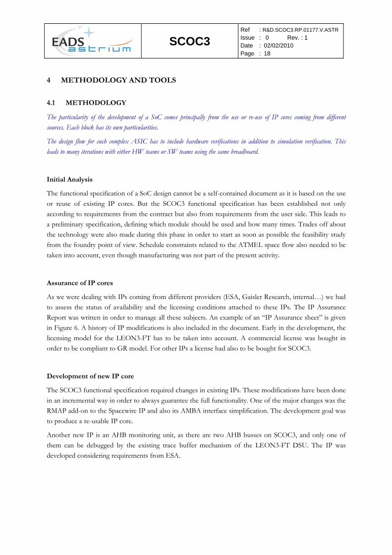
The functional specification of a SoC design cannot be a self-contained document as it is based on the use or reuse of existing IP cores. But the SCOC3 functional specification has been established not only according to requirements from the contract but also from requirements from the user side. This leads to a preliminary specification, defining which module should be used and how many times. Trades off about the technology were also made during this phase in order to start as soon as possible the feasibility study from the foundry point of view. Schedule constraints related to the ATMEL space flow also needed to be taken into account, even though manufacturing was not part of the present activity.
Assurance of IP cores
As we were dealing with IPs coming from different providers (ESA, Gaisler Research, internal…) we had to assess the status of availability and the licensing conditions attached to these IPs. The IP Assurance Report was written in order to manage all these subjects. An example of an “IP Assurance sheet” is given in Figure 6. A history of IP modifications is also included in the document. Early in the development, the licensing model for the LEON3-FT has to be taken into account. A commercial license was bought in order to be compliant to GR model. For other IPs a license had also to be bought for SCOC3.
Development of new IP core
The SCOC3 functional specification required changes in existing IPs. These modifications have been done in an incremental way in order to always guarantee the full functionality. One of the major changes was the RMAP add-on to the Spacewire IP and also its AMBA interface simplification. The development goal was to produce a re-usable IP core.
Another new IP is an AHB monitoring unit, as there are two AHB busses on SCOC3, and only one of them can be debugged by the existing trace buffer mechanism of the LEON3-FT DSU. The IP was developed considering requirements from ESA.

SCOC3 Ref : R&D.SCOC3.RP.01177.V.ASTR Issue : 0 Rev. : 1 Date : 02/02/2010 Page : 19
Spacewire I/F Function Spacewire I/F implementing ECSS-E50-12 standard Status Modified in this R&D Used in SCOC1 Yes Provider Astrium Distribution N.A. License Type (b) modified in this contract delivery Source code Modifications to be performed to the IP • The previous IP had 3 ports on AHB bus (2 masters for DMA transmit and receive, 1 slave for transmit). The slave I/F is suppressed. The two masters are merged into one. • RMAP protocol is implemented Verification status • Will be verified in this R&D Known use and experiences • Tested in SCOC1 and by various users in Europe since Spacewire IP belongs to ESA catalog
Figure 6 : Spacewire assurance report sheet
Like on this table, there is for each block, a table which gives the main information according to ownership, licensing, background, verification status…
Figure 7 : Overview of the SCOC3 testbench structure
Most of the emulator composing the SCOC3 testbench are issued and re-used from the IP core testbench. The standardization of emulators allows inter-operability at upper level. The TM emulator is in fact an instantiation of functions provided with the
PTME IP. The controller emulator allows synchronisation of the emulators altogether.

SCOC3 Ref : R&D.SCOC3.RP.01177.V.ASTR Issue : 0 Rev. : 1 Date : 02/02/2010 Page : 20
Architectural Design
During the architectural design phase, the IP cores were developed according to their detailed specification, and the IP cores were integrated into the overall architecture of SCOC3.
The detailed architecture of each IP core is provided in IP specific documents, and the overall SCOC3 architectural design document refers to these IP documents.
For the simulations, the main point is the re-use (and eventually porting) of simulation environments from the IP core up to the system level. The simulation environment is illustrated in Figure 7. It uses emulators which are driven by text-based scripts.
Verification Plans have been written, one more specifically for simulation: SCOC3 Simulation Plan and Report and one more dedicated to the prototyping board: HW/SW verification plan.
Hardware Prototyping
Prototyping has been performed using a commercial Virtex4LX200 FPGA on the KerDive board shown in Figure 8. This FPGA allows us to wholly integrate the SCOC3 and tests most of its functionalities on a board. We also used the MAEVA board from a previous development to test the SRAM interface. This was an iterative process, allowing quick bug fixes, and we had the feedback of SW teams, doing preliminary SW development using an identical board.
Gate Level Design
The Gate Level Design has been made as far as to allow the Logic Review according to ATMEL flow. This means that we have made the Design Start Review and the Feasibility Review during this phase. We also made any simulations, timing analysis and synthesis in the targeted ATC18RHA ATMEL technology. We had many exchanges with the ATMEL design centre in order to be ready for the Logic Review.
4.2 TOOLS
SCOC3 development has been using software tools for classical ASIC development. This section aims to discuss on each of these tools, mainly VHDL simulator and synthesis tool when used to develop SCOC.3
Simulation tool
A commonly used VHDL simulation tool used is Mentor Modelsim (Figure 9). This tool is well suited for verification of SCOC3 at RTL level. A standardization of the methodology used for the development of testbench as well as basic rules for the VHDL RTL description eases the simulation of complex SOC.
Synthesis tools
Synplify is a powerful synthesis tool for quick FPGA development. The TCL scripting possibilities ease the use of this tool for complex SoC designs. We also use Synopsys for the ASIC technology with the 3.2 ATMEL design kit. Prime Time was also used to get the accurate timing margin in order to be ready for the Logic Review.

SCOC3 Ref : R&D.SCOC3.RP.01177.V.ASTR Issue : 0 Rev. : 1 Date : 02/02/2010 Page : 21
ACTEL FPGA RU
SCOC3 Memories banks SCOC3 EEPROM bank
Virtex4 LX200 for SCOC3 integration
Figure 8 : KerDive board
The KerDive board integrates all environments necessary to evaluate the SCOC3 in a dedicated application test environment.
Figure 9 : Overview of the Modelsim simulation
Wave signals show LEON PC (Program Counter), INST (Instr. code), CWP (Current Window Pointer), TT (Trap Type) registers and both AHB busses.

SCOC3 Ref : R&D.SCOC3.RP.01177.V.ASTR Issue : 0 Rev. : 1 Date : 02/02/2010 Page : 22
5 EVOLUTION OF STUDY
Follow-up activities will include the ASIC layout and manufacturing in the frame of ATMEL space MPW programme, validation, and the development of SW tools and drivers. The final goal is to establish SCOC3 as a standard component (ASSP) greatly available to all users in the ESA member and participating states.
6 CONCLUSION
The study performed for this contract puts in evidence the absolute necessity of a reliable and effective design methodology of SoC development. It allows speeding up the architectural development phase of a large design as shown for the development of SCOC3.
This methodology is mainly based on the availability for the European space community of a library of validated IP cores. This is now well supported by ESA, as indicated by the development of the PTME, the Spacewire IP, the HurriCAN controller and a collection of small but indispensable IP. It also relies on the commercial set of IPs and main processing function coming from Gaisler Research: GRLIB and LEON3-FT.
The methodology also takes advantage from standards coming from commercial applications, military developments or space industry, such as AMBA busses for internal connections of the IP cores, and also external interface standards, that allows the reuse of the developed IP core, Mil-Std-1553, Spacewire, CCSDS TM/TC. This strategy was beneficial for SCOC3 development as it allowed reusing already developed validation tools (emulators for the simulations and standard hardware testbenches for the board evaluation).
The promotion for using these standards for ESA programmes is absolutely necessary to enhance the catalogue of available IP cores and the availability of verification/validation tools.
The availability of large commercial programmable logic devices is beneficial. They allow rapid prototyping of the system and a deeper functional validation than using only simulations. FPGA prototyping also provides a breadboard platform for early software development, well before the availability of the System-On-ASIC.
The development of a prototyping hardware platform does not suppress the essential simulation phase. Nevertheless, due to the complexity of SCOC3, the simulation time dramatically increases (while partially compensated by the increase of the simulation platform computation performances). The simulations are then used to fully verify the IP core functionality in a standalone mode, while the system simulations only partially verify the core functionality of each IP, focusing on the correct integration of SCOC3. But is has to be noticed that a very big set of simulations has been used in order to increase confidence and allow early bug detection/investigation.
SCOC3 Ref : R&D.SCOC3.RP.01177.V.ASTR Issue : 0 Rev. : 1 Date : 02/02/2010 Page : 23
The main conclusions of the SCOC3 activity are then:
• The architectural design of SCOC3 has been developed. It uses existing IP cores from Astrium, ESA and Aeroflex-Gaisler, some of them were modified, other IP cores were newly developed.
• The architectural design was verified by extensive simulation, by FPGA prototyping, and by development with software teams.
• The software tools already used for the ASIC development (for VHDL simulation and synthesis) are still suitable to the development of SoC, provided proper scripting is used.
• Hardware prototyping of the SoC using large commercial FPGA greatly improves the system verification, compensating for the reduction of verification coverage of post layout simulations.
• The development of SoC including the CPU core such as the designed SCOC3 is crucial for the development of future small space platforms and probes.
• There is a great interest of the SoC methodology for the future development of highly integrated ASIC, including or not the CPU core.
• The methodology of IP reuse has to be promoted by the Agency in order to complete the already available catalogue of IP cores, and to enhance the verification level of these IPs.
---%---%---%---%---