modeling, analysis and design of synchronous buck ...ethesis.nitrkl.ac.in/5338/1/109ee0518.pdf ·...
TRANSCRIPT

Modeling, Analysis and Design of Synchronous Buck
Converter Using State Space Averaging Technique for PV
Energy System.
GUNDA SUMAN (109EE0519)
B.V.S PAVAN KUMAR (109EE0518)
M SAGAR KUMAR (109EE0153)
Department of Electrical Engineering
National Institute of Technology Rourkela

- 2 -
MODELING, ANALYSIS AND DESIGN OF
SYNCHRONOUS BUCK CONVERTER USING STATE
SPACE AVERTAGING TECHNIQUE FOR
PV ENERGY SYSTEM
A Thesis submitted in partial fulfillment of the requirements for the degree of
Bachelor of Technology in “Electrical Engineering”
By
GUNDA SUMAN (109EE0519)
B.V.S PAVAN KUMAR (109EE0518)
M SAGAR KUMAR (109EE0153)
Under guidance of
Prof. K.R.SUBHASHINI
&
Prof. B.CHITTI BABU
Department of Electrical Engineering
National Institute of Technology
Rourkela-769008 (ODISHA)
May-2011

- 3 -
DEPARTMENT OF ELECTRICAL ENGINEERING
NATIONAL INSTITUTE OF TECHNOLOGY, ROURKELA- 769 008
ODISHA, INDIA
CERTIFICATE
This is to certify that the draft report/thesis titled “Modeling, Analysis and Design of
Synchronous Buck Converter Using State Space Averaging Technique for PV Energy System”,
submitted to the National Institute of Technology, Rourkela by Gunda Suman (Roll. No.
109ee0519), B.V.S Pavan Kumar (Roll. No. 109ee0518) and M Sagar Kumar (Roll. No. 109ee0153)
for the award of Bachelor of Technology in Electrical Engineering, is a bonafide record of research
work carried out by him under my supervision and guidance.
The candidate has fulfilled all the prescribed requirements.
The draft report/thesis which is based on candidate’s own work, has not submitted elsewhere
for a degree/diploma.
In my opinion, the draft report/thesis is of standard required for the award of a Bachelor of
Technology in Electrical Engineering.
Prof. K.R.Subhashini
Supervisor
Prof. B.Chitti Babu
Co-Supervisor

a
ACKNOWLEDGEMENTS
For the development of the whole prodigious project of “Modeling, Analysis and Design
of Synchronous Buck Converter Using State Space Averaging Technique for PV Energy
System”, we would like to extend our gratitude and our sincere thanks to our supervisors Prof.
K.R.Subhashini, Asst. Professor, Department of Electrical Engineering and Prof. B.Chitti Babu,
Asst. Professor, Department of Electrical Engineering for their constant motivation and support
during the course of our work in the last one year. We truly appreciate and value their esteemed
guidance and encouragement from the genesis to the apocalypse of the project. From the bottom
of our heart we express our gratitude to our beloved professors for being lenient, consoling and
encouraging when we were going through pressured phases during placements.
We are very thankful to our teachers Dr. B.D.Subudhi and Prof. A.K.Panda for providing
solid background for our studies, with their exemplary class room teaching. And also Prof.
S.Samanta for his exquisite teaching of MATLAB and Simulink during Lab sessions. They have
great sources of inspiration to us and we thank them from the bottom of our hearts.
At last but not least, we would like to thank the staff of Electrical engineering department
for constant support and providing place to work during project period. Especially I want to
acknowledge the help of Mr.Gangadhar Bag, Lab Asst., Dept. of Electrical Engineering for his
assiduous help during experimental work. We would also like to extend our gratitude to our
friends, especially Satarupa Bal and Anup Anurag whose knowledge and help was the pioneer
reason for us to be successful during experimental work, despite of our skeptic attitude.
Gunda Suman
B.V.S Pavan Kumar
M Sagar Kumar
B.Tech (Electrical Engineering)

b
Dedicated to,
Our Parents & friends who has been there
for us from genesis to apocalypse…

i
ABSTRACT
If we start forecasting in the view of electrical energy generation, in the upcoming decade
all the fossil fuels are going to be extinct or the worst they are going to be unaffordable to a person
living in typical circumstances, so renewable power energy generation systems are going to make
a big deal out of that. It is extremely important to generate and convert the renewable energy with
maximum efficiency. In this project, first we study the characteristics of low power PV array under
different values of irradiance and temperature. And then we present the exquisite design of
Synchronous Buck Converter with the application of State Space Modeling to implement precise
control design for the converter by the help of MATLAB/Simulink. The Synchronous Buck
Converter thus designed is used for portable appliances such as mobiles, laptops, iPod’s etc. But
in this project our main intention is to interface the PV array with the Synchronous Buck Converter
we designed, and we will depict that our converter is more efficient than the conventional buck
converter in terms of maintaining constant output voltage, overall converter efficiency etc. And
then we show that the output voltage is maintaining constant irrespective of fluctuations in load
and source. And finally we see the performance of Synchronous Buck Converter, which is
interfaced with PV array having the practical variations in temperature and irradiance will also
maintain a constant output voltage throughout the response. All simulations are carried under
MATLAB/Simulink environment.
And at last experimental work is carried out for both conventional buck converter and also
for synchronous buck converter, in which we observe the desired outputs obtained in simulations.

ii
CONTENTS
Abstract i
Contents ii
List of Figures v
Abbreviations and Acronyms vi
CHAPTER 1
INTRODUCTION
1.1 Motivation 2
1.2 PV Energy 2
1.2.1 Photovoltaics(PV) 2
1.2.2 PV Energy Efficiency 3
1.3 Synchronous Buck Converter – An Introduction 4
1.4 Overview Of Proposed Work done 5
1.5 Thesis Objectives 6
1.6 Organization of Thesis 6
CHAPTER 2
PV-ARRAY CHARACTERISTICS
2.1 Introduction 9
2.2 PV Array Modeling 9

iii
CHAPTER-3
STATE SPACE MODELING OF SYNCHRONOUS BUCK CONVERTER
3.1 MOTIVATION 13
3.2 STATE SPACE MODELING 14
3.2.1 ON-State Equations 15
3.2.2 OFF-State Equations 17
CHAPTER-4
SYNCHRONOUS BUCK CONVERTER AND IT’S EFFICIENCY
4.1 Synchronous Buck Converter Design 20
4.2 Synchronous Buck Converter Efficiency and Comparison 23
CHAPTER-5
MAXIMUM POWER POINT TRACKING (MPPT)
5.1 Introduction 26
5.2 Perturb & Observe Method 28
5.2.1 Motivation 28
5.2.2 Hill Climbing Techniques 28
5.2.3 P & O Algorithm Implementation 29
CHAPTER-6
RESULTS AND DISCUSSION
6.1 PV System 32
6.2 Closed loop Bode Plot of Synchronous Buck Converter 34

iv
6.3 Synchronous Buck Converter 35
6.3.1 During Steady State Conditions 35
6.3.2 During Step Changes in Load 36
6.3.3 During Variation of Solar Irradiation and Temperature 37
6.4 Efficiency Comparison 37
6.5 Maximum Power Point Tracking 38
6.6 Experimental Results 39
6.6.1 Conventional Buck Converter 40
6.6.2 Synchronous Buck Converter 42
CONCLUSIONS 44
References 45
Publications 46

v
LIST OF FIGURES
Fig. No Name of the Figure Page. No.
1 Schematic Diagram of PV Based Converter System. 4
2 Equivalent Circuit of PV Cell 10
3 Schematic of closed loop control algorithm of Synchronous Buck
Converter 14
4 On-State Circuit Diagram of Synchronous Buck Converter 15
5 Off-State Circuit Diagram of Synchronous Buck Converter 17
6 Block diagram of DC-DC converter incorporating MPPT control 27
7 Flow Chart of P&O Algorithm 29
8 I-V Characteristics at Constant Temperature 32
9 P-V Characteristics at Constant Temperature 33
10 I-V Characteristics at Constant Irradiance 33
11 P-V Characteristics at Constant Irradiance 34
12 Bode plot of PI controller for Frequency Response 34
13 Steady state response of Synchronous Buck Converter 35
14 Response due to Step Changes in the Load 36
15 Dynamics of Synchronous Buck Converter 37
16 Efficiency Comparison between Synchronous Buck Converter and
Conventional Buck Converter. 38
17 Response of Synchronous Buck Converter using MPPT technique 39
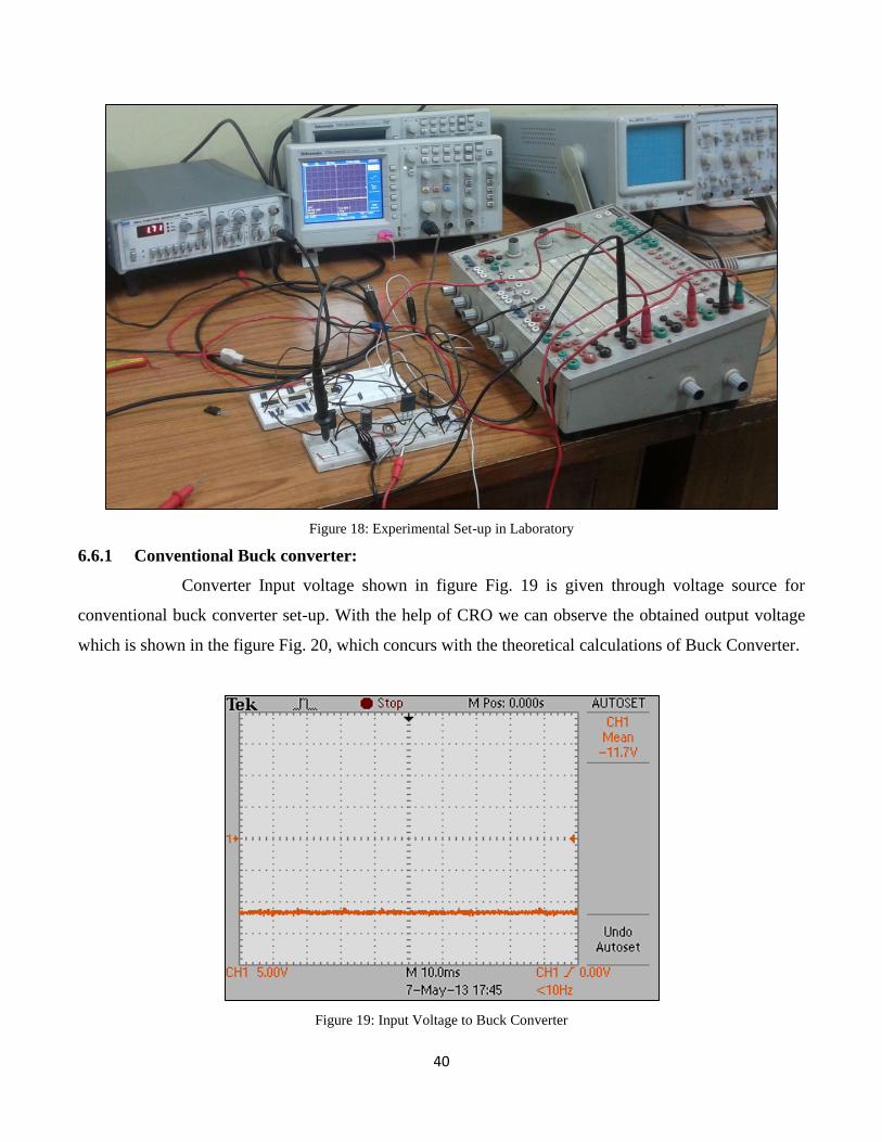
18 Experimental Set-up in Laboratory 40
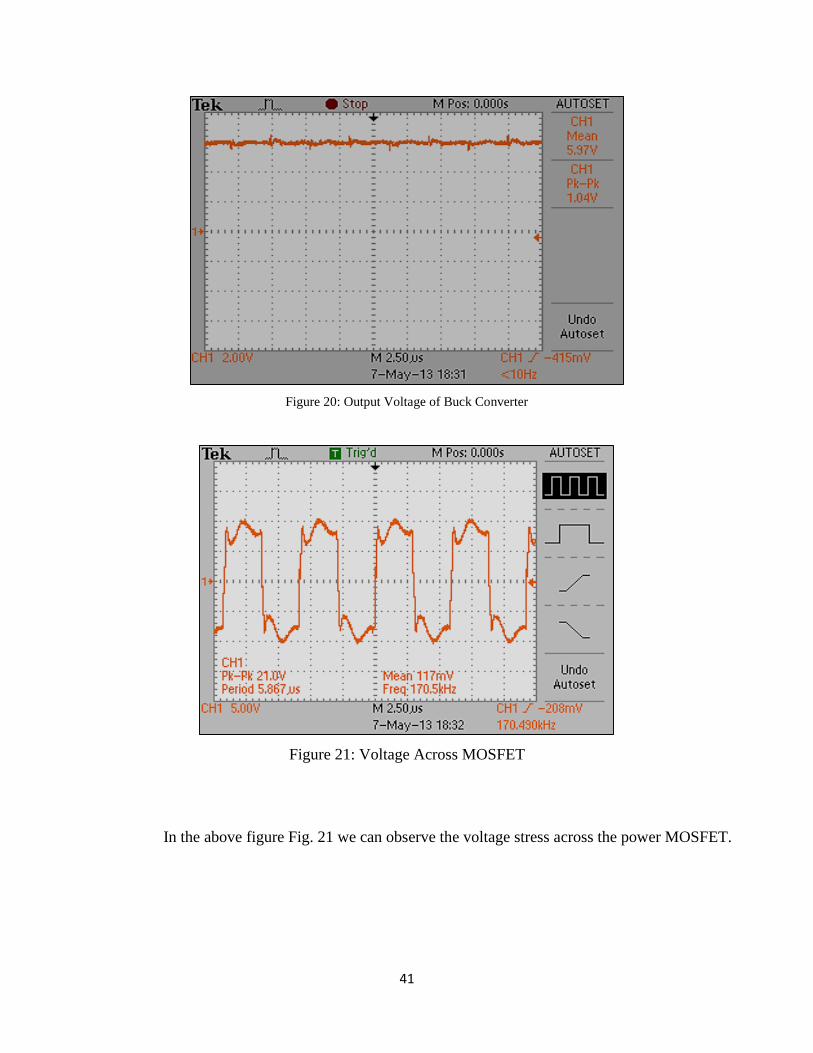
19 Input Voltage of Buck Converter 40
20 Output Voltage of Buck Converter 41
21 Voltage across MOSFET 41
22 Output Voltage for Synchronous Buck Converter 42
23 Voltage across Main MOSFET M1 43
24 Voltage across Synchronous MOSFET M2 43
vi
ABBREVIATIONS AND ACRONYMS
MNRE - Ministry of New and Renewable Energy
IREDA - Indian Renewable Energy Development Agency
PVA - Photo Voltaic Array
AC - Alternating Current
DC - Direct Current
SPV - Solar Photo Voltaic
MOSFET - Metal Oxide Semiconductor Field Effect Transistor
PWM - Pulse Width Modulation
EMI - Electro Magnetic Interference
MATLAB - MATrixLABoratory
MPPT - Maximum Power Point Tracking
PID - Proportional, Integral and Derivative
IC - Integrated Circuit
LED - Light Emitting Diode
SMPS - Switched Mode Power Supply

1
CHAPTER 1
Introduction

2
1.1 MOTIVATION:
As the days go by, the demand of power is increasing gradually and on the contrary the
resources used for power generation are becoming inadequate. Apart from the reason of inadequate
resources, the methods used for power generation by fossil fuels are not even environment friendly
and they devote an ultimate reason for global warming and greenhouse effect.
So it is the time to initiate the usage of renewable energy resources on very large scale.
The three main available renewable energy resources are (i) Direct Solar Energy, (ii) Hydro Energy
and (iii) Wind Energy. Hydro Energy generation and Wind Energy generation are of course two
of the main sources of renewable energies, but the main disadvantage in Hydro Energy is that, it
is seasonal dependent and in Wind energy is that it is geographical location dependent [1]. On the
other hand Solar Energy is prevalent all over the globe and all the time. The amount of irradiance
and temperature may vary from place to place and from time to time but under given conditions
Solar Energy system can be implemented. Solar Energy or PV energy system is the most direct
way to convert the solar radiation into electricity based on photovoltaic effect. Despite of high
initial costs, they are already have been implemented in many rural areas. In future the cost of the
PV panel also may diminish, because of the advancing technology and also the competition
between manufacturers. And therefore, the time is not so far that almost every middle class person
can afford his own solar panel at home for at least some basic requirements.
In the perspective of above noted points, it is evident that PV Energy plays a pioneer role
in the forthcoming future. So, it is our duty to learn, implement and improvise the idea as fast as
we can, so that it becomes prevalent rather than precarious to the future generations.
1.2 PV ENERGY:
1.2.1 Photovoltaics (PV):
Photovoltaics are best known as a method for generating electric power by using solar cells
to convert energy from the sun into a flow of electrons. The photovoltaic effect refers to photons
of light exciting electrons into a higher state of energy, allowing them to act as charge carriers for

3
an electric current. The photovoltaic effect was first observed by Alexandre-Edmond Becquerel in
1839.The term photovoltaic denotes the unbiased operating mode of a photodiode in which current
through the device is entirely due to the transduced light energy. Virtually all photovoltaic devices
are some type of photodiode.
Solar cells produce direct current electricity from sun light which can be used to power
equipment or to recharge a battery. The first practical application of photovoltaic was to power
orbiting satellites and other spacecraft, but today the majority of photovoltaic modules are used
for grid connected power generation. In this case an inverter is required to convert the DC to AC.
There is a smaller market for off-grid power for remote dwellings, boats, recreational vehicles,
electric cars, roadside emergency telephones, remote sensing, and cathodic protection of pipelines.
Cells require protection from the environment and are usually packaged tightly behind a
glass sheet. When more power is required than a single cell can deliver, cells are electrically
connected together to form photovoltaic modules, or solar panels. A single module is enough to
power an emergency telephone, but for a house or a power plant the modules must be arranged in
multiples as arrays.
1.2.2 PV Energy Efficiency:
The output voltage thus obtained from the PV panel is DC. For low power applications,
dc-dc converters are employed to step-up or step-down the output DC voltage according to the
load requirements. However overall conversion efficiency is very low (typically 6.5 percent). So
accurate modeling and design of dc-dc converter is necessary in order to improve the overall
system performance with cost effective solution [2].
As the efficiency of solar panel itself is very less and it is inevitable, so the precaution
should be taken such that the efficiency of the converter should be maximum. For the efficient
regulation of output DC voltage, Synchronous Buck Converter is designed in the project. Various
converter topologies have been proposed in the literature.
4
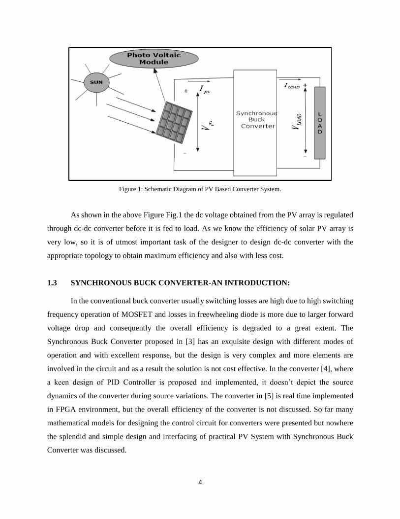
Figure 1: Schematic Diagram of PV Based Converter System.
As shown in the above Figure Fig.1 the dc voltage obtained from the PV array is regulated
through dc-dc converter before it is fed to load. As we know the efficiency of solar PV array is
very low, so it is of utmost important task of the designer to design dc-dc converter with the
appropriate topology to obtain maximum efficiency and also with less cost.
1.3 SYNCHRONOUS BUCK CONVERTER-AN INTRODUCTION:
In the conventional buck converter usually switching losses are high due to high switching
frequency operation of MOSFET and losses in freewheeling diode is more due to larger forward
voltage drop and consequently the overall efficiency is degraded to a great extent. The
Synchronous Buck Converter proposed in [3] has an exquisite design with different modes of
operation and with excellent response, but the design is very complex and more elements are
involved in the circuit and as a result the solution is not cost effective. In the converter [4], where
a keen design of PID Controller is proposed and implemented, it doesn’t depict the source
dynamics of the converter during source variations. The converter in [5] is real time implemented
in FPGA environment, but the overall efficiency of the converter is not discussed. So far many
mathematical models for designing the control circuit for converters were presented but nowhere
the splendid and simple design and interfacing of practical PV System with Synchronous Buck
Converter was discussed.

5
Synchronous MOSFET is clamped by a Schottky rectifier; it prevents the MOSFET’s
intrinsic body diode from conducting which prevents the body diode from developing a stored
charge. The body diode in a MOSFET is a slow rectifier and would add significant losses if it were
allowed to switch. Because the MOSFET rectifier (synchronous rectifier) switches with less than
a volt across itself, the switching losses are almost zero compared to conduction losses. And then
we conclude that the Synchronous Buck Converter obtained by clamping Schottky rectifier across
synchronous switch is far more efficient.
1.4 OVERVIEW OF PROPOSED WORK DONE:
Many literatures are used to carry out the project which includes notes on photovoltaic
arrays, PV energy systems, converters topology, variation in the performance of arrays with
atmospheric conditions, etc. Reference [1]-[6] gives an overview about the applications of
photovoltaic technology. Reference [7] tells about the converter requirement for photovoltaic
applications. Various converter topologies have been proposed in the available literature [8]-[9]
which describe various such converters available for use. In the conventional buck converter
usually switching losses are high due to high switching frequency operation of MOSFET and
losses in freewheeling diode is more due to larger forward voltage drop and consequently the
overall efficiency is degraded to a great extent. The Synchronous Buck Converter proposed in [3]
has an exquisite design with different modes of operation and with excellent response, but the
design is very complex and more elements are involved in the circuit and as a result the solution
is not cost effective. In the converter [4], where a keen design of PID Controller is proposed and
implemented, it doesn’t depict the source dynamics of the converter during source variations. The
converter in [5] is real time implemented in FPGA environment, but the overall efficiency of the
converter is not discussed. So far many mathematical models for designing the control circuit for
converters were presented but nowhere the splendid and simple design and interfacing of practical
PV System with Synchronous Buck Converter was discussed.
We later extend our converter design to closed loop design using mathematical State Space
Modeling. And the study of Maximum Power Point Tracking (MPPT) in PV Energy Systems, and
also to be implemented in the proposed converter.

6
1.5 THESIS OBJECTIVES:
The objectives are hopefully to be achieved at the end of the project:
1. To study the solar cell model and observe its characteristics.
2. To study the proposed synchronous DC-DC buck converter and its operation.
3. To study the design of closed loop with controller with the help of State-Space
Modeling.
4. To study the comparison between the conventional DC-DC buck converter and the proposed
synchronous DC-DC buck converter in terms of efficiency improvement.
5. To study the Maximum Power Point Tracking (MPPT) algorithms of PV Energy system and
to implement in Simulink Environment.
6. To validate the experimental results obtained from the laboratory set-up and to analyze the
results with the simulated results in the MATLAB-Simulink Environment.
1.6 ORGANISATION OF THESIS:
The thesis is organized into six chapters including the chapter of introduction. Each chapter
is different from the other and is described along with the necessary theory required to comprehend
it.
Chapter No.2 deals with PV Array Characteristics and its modelling. First, the equivalent
mathematical modelling of the solar cell is made after studying various representations and
simplification is made for our purpose. Then PV and IV characteristics curves for both constant
temperature and constant irradiation for the equivalent model is studied in MATLAB-Simulink
environment using the equation corresponding to that model.
Chapter No.3 deals with the design of various components of Synchronous Buck Converter
such as inductor, input capacitor, output capacitor, MOSFET etc., and this section also deals with
the comparison between Synchronous Buck Converter and Conventional Buck Converter,
especially in the perspective of efficiency.

7
Chapter No.4 deals with the whole concept of State Space Modeling, and merits of it. And
eventually state space equations of the proposed Synchronous Buck Converter is derived in this
section, thus obtaining A,B,C and D matrices for the later evaluations during control feedback
designing. Which later on used to study the Steady State Response, Response during Step changes
in load, Dynamic response while considering the effect of temperature and irradiance changes
which effects the input voltage of Synchronous Buck Converter.
Chapter No.5 deals with the study of Maximum Power Point Tracking and its significance
in PV Energy systems. And later on we adopt P and O algorithm in MATLAB/Simulink to design
the MPPT controller to track and operate at maximum power point for the proposed PV Energy
system.
Chapter No.6 is results and discussion section, in which all simulation results such as PV
Characteristics, Steady State Simulation of converter, and Simulation during step changes in load
of converter, Dynamic operation of converter, efficiency comparison etc., which are obtained in
before sections are displayed and explained each result meticulously. Also the experimental results
for conventional buck converter and synchronous buck converter are depicted and elucidated.

8
CHAPTER 2
PV-Array Characteristics

9
2.1 INTRODUCTION:
Learning and analyzing PV Array characteristics plays a vital role when it comes to PV energy
generation. These characteristics vary from one model to the other. But, however we in this section study
the PV array characteristics for ideal PV Cell, which includes P-V and I-V characteristics during constant
temperature and also P-V and I-V characteristics during constant Irradiance. Meticulous study of these
characteristics helps us to understand the functioning of PV Cell during the variations of temperature and
irradiation which are the pioneer parameters for PV energy generation.
These characteristics obtained, not only helps us in understanding PV system, but also helps in the
study of concept Maximum Power Point Tracking (MPPT) and also to obtain that point for maximum
efficient operation of System. These topics are discussed in later chapters in detail.
2.2 PV ARRAY MODELING:
The solar cell arrays or PV arrays are usually constructed out of small identical building blocks of
single solar cell units. They determine the rated output voltage and current that can be drawn for a given
set of atmospheric data. The rated current is given by the number of parallel paths of solar cells and the
rated voltage of the array depends on the number of solar cells connected in series in each of the parallel
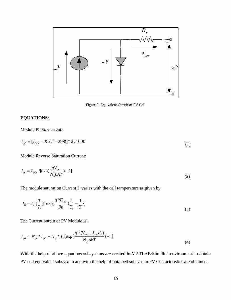
paths. A single PV cell is a photodiode. The single cell equivalent circuit model consists of a current
source dependent on irradiation and temperature, a diode that conducts reverse saturation current, forward
series resistance of the cell.
In the Figure 2, is an approximated version of actual single cell equivalent circuit, the output
current (Ipv) and the output voltage (Vpv) are dependent on the solar irradiation and temperature and also
the saturation current of diode. For that single cell, Ipv and Vpv are calculated by the equations given below:
10
Figure 2: Equivalent Circuit of PV Cell
EQUATIONS:
Module Photo Current:
1000/*)]298([ TKII iSCrph (1)
Module Reverse Saturation Current:
]1)/[exp( kATN
qVII
s
OCSCrrs
(2)
The module saturation Current I0 varies with the cell temperature as given by:
}]11
{*
exp[][03
0TTBk
Eq
T
TII
r
g
r
rs
(3)
The Current output of PV Module is:
]1})(*
[exp{** 0
AkTN
RIVqININI
s
spvpv
pphppv
(4)
With the help of above equations subsystems are created in MATLAB/Simulink environment to obtain
PV cell equivalent subsystem and with the help of obtained subsystem PV Characteristics are obtained.

11
The solar array mainly depends up on three factors: (i) Load current, (ii) Ambient temperature and (iii)
Solar irradiation. They are observed as,
(i) When load current increases the voltage drops in the PV array.
(ii) When the temperature increases the output power reduces due to increased internal resistance across
the cell.
(iii) When irradiation level increases, the output power increases as more photons knock out electrons and
more current flow causing greater recombination.
The variation of output power acts as a function of cell voltage and is affected by different operating
conditions. Also output I-V characteristics of the single cell model are observed under various conditions
of temperature and solar irradiation. The concerned simulations results are obtained under MATLAB-
Simulink environment and are given in results and discussion section.
The obtained results are depicted in the RESULTS AND DISCUSSION Section, under the figure numbers
Fig. 8, Fig. 9, Fig. 10 and Fig. 11

12
CHAPTER 3
State Space Modelling of
Synchronous Buck Converter

13
3.1 MOTIVATION:
The performance of closed loop converter is highly influenced by PI control parameters. Auto
tuning controller improves dynamic response efficiency and reliability. The main idea of auto-tuning is
presented as: first system identification is executed and then control parameters are tuned [10].Various
methods are introduced to adjust the controller terms. In our project, mathematical modeling of buck
converter using State space averaging technique is implemented for this purpose. From the above obtained
A, B, C and D matrices, we can obtain the KP and KI values of the PI Controller by State space modeling
of synchronous buck converter using MATLAB commands ‘sys=ss(A,B,C,D)’ and ’sisotool(sys)’. Then
by the result windows obtained by sisotool we select the automated PID tuning option to obtain the KP
and KI values, and which includes the frequency response of closed loop system. SISO design tool
automatically designs interactive compensator design.
The complete closed loop control structure of synchronous buck converter is illustrated in Fig. 3
and the load voltage is compared with reference value, error voltage is generated. The resultant error is
fed to PI controller. PI Controller attempts to correct the error between voltage variable measured and a
desired voltage (reference) value by calculating and then outputting a corrective action that can adjust the
process accordingly. As we know PI controller involves two separate variables: the Proportional and the
Integral values. The integral term added to the proportional term accelerates the movement of process
towards reference voltage and eliminates the residual steady-state error that occurs with a P controller.
The amplified error voltage so obtained is passed through Hysteresis control limiter which limits the value
obtained by PID controller to certain value. By using pulse-width modulation (PWM) control regulation
of output voltage is achieved by varying the duty cycle of the switches synchronously.
This whole process is possible only after the calculation of state space matrices A, B, C and D,
whose derivations are elucidated in the following section.

14
Figure 3: Schematic of closed loop control algorithm of Synchronous Buck Converter.
3.2 STATE SPACE MODELING:
In order to analyze our system, it is essential to reduce the complexity of the mathematical
expressions, as well as to resort to computers for most of the tedious computations necessary in the
analysis, state-space approach is best suited for this purpose [10]. In literature this state space averaging
is the modeling structure given.
Since there is the presentation of accurate mathematical modeling of the system, it helps us
obtaining precise KP and KI values during PID tuning, which in turn plays a major role in the accurate and
exquisite response of closed loop system.
To get proper dynamic equation for synchronous buck converter, we define the two phase of
switches (ON and OFF). The network has two energy storage elements: a capacitor C and an inductor L.
Assuming voltage across capacitor and current through inductor at t=0 is zero. The only means of selection
of state variables is IL and VC.
15
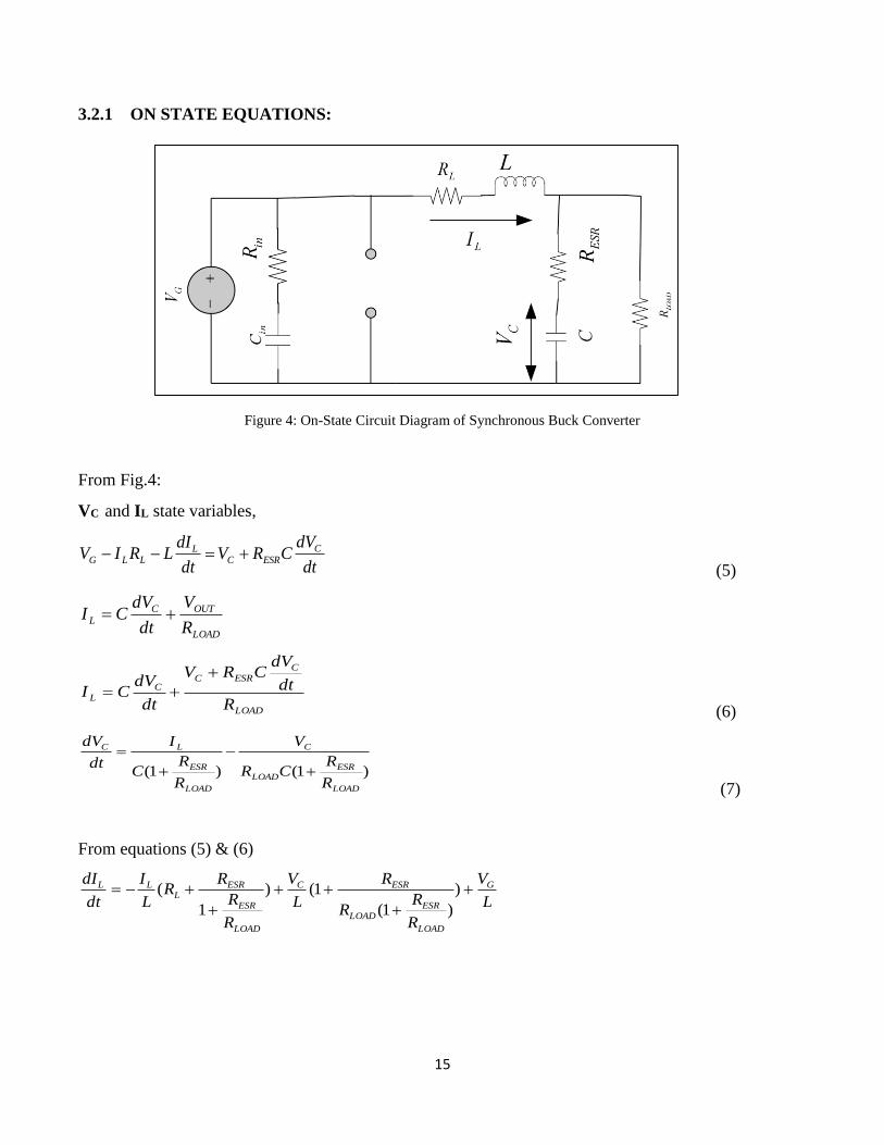
3.2.1 ON STATE EQUATIONS:
Figure 4: On-State Circuit Diagram of Synchronous Buck Converter
From Fig.4:
VC and IL state variables,
dt
dVCRV
dt
dILRIV C
ESRCL
LLG (5)
LOAD
OUTCL
R
V
dt
dVCI
LOAD
CESRC
CL
R
dt
dVCRV
dt
dVCI
(6)
)1()1(LOAD
ESRLOAD
C
LOAD
ESR
LC
R
RCR
V
R
RC
I
dt
dV
(7)
From equations (5) & (6)
L
V
R
RR
R
L
V
R
R
RR
L
I
dt
dI G
LOAD
ESRLOAD
ESRC
LOAD
ESR
ESRL
LL
)
)1(
1()
1
(

16
From above equation (7)
G
C
L
LOAD
ESRLOAD
LOAD
ESR
LOAD
ESRLOAD
ESR
LOAD
ESR
ESRL
C
L
V
L
V
I
R
RCR
R
RC
R
RR
R
L
R
R
RR
L
dt
dV
dt
dI
0
1
)1(
1
)1(
1
)
)1(
1(1
)
1
(1
G
LOAD
ESRLOAD
LOAD
ESR
LOAD
ESRLOAD
ESR
LOAD
ESR
ESRL
V
L
X
X
R
RCR
R
RC
R
RR
R
L
R
R
RR
L
X
X
0
1
)1(
1
)1(
1
)
)1(
1(1
)
1
(1
2
1
2
1
From Fig.4:
dt
dVCRVV C
ESRCOUT (8)
From equation (7) & (8)
)
1
()
)1(
1(
LOAD
ESR
ESRL
LOAD
ESRLOAD
ESRCOUT
R
R
RI
R
RR
RVV
(9)
C
L
LOAD
ESRLOAD
ESR
LOAD
ESR
ESROUT
V
I
R
RR
R
R
R
RV
)1(
1
1
U
X
X
R
RR
R
R
R
RY
LOAD
ESRLOAD
ESR
LOAD
ESR
ESR
0
0
)1(
1
1
2
1

17
3.2.2 OFF STATE EQUATIONS:
Fig.5: Off-State Circuit Diagram of Synchronous Buck Converter
From Fig. 5:
LOAD
OUTCL
R
V
dt
dVCI
(10)
dt
dVCRV
dt
dILRI C
ESRCL
LL (11)
dt
dVCRVV C
ESRCOUT (12)
From equations (10) & (12)
)1()1(LOAD
ESRLOAD
C
LOAD
ESR
LC
R
RCR
V
R
RC
I
dt
dV
(13)
From equations (11) & (13)
)
)1(
1()
1
(
LOAD
ESRLOAD
ESRCL
LOAD
ESR
ESRLL
R
RR
R
L
VR
R
R
R
L
I
dt
dI
(14)

18
From above equations (13) & (14)
G
C
L
LOAD
ESRLOAD
LOAD
ESR
LOAD
ESRLOAD
ESR
LOAD
ESR
ESRL
C
L
V
L
V
I
R
RCR
R
RC
R
RR
R
L
R
R
RR
L
dt
dV
dt
dI
0
1
)1(
1
)1(
1
)
)1(
1(1
)
1
(1
G
LOAD
ESRLOAD
LOAD
ESR
LOAD
ESRLOAD
ESR
LOAD
ESR
ESRL
V
L
X
X
R
RCR
R
RC
R
RR
R
L
R
R
RR
L
X
X
0
1
)1(
1
)1(
1
)
)1(
1(1
)
1
(1
2
1
2
1
From Fig.5:
dt
dVCRVV C
ESRCOUT
From equations (12) & (13)
)
1
()
)1(
1(
LOAD
ESR
ESRL
LOAD
ESRLOAD
ESRCOUT
R
R
RI
R
RR
RVV
(15)
U
X
X
R
RR
R
R
R
RY
LOAD
ESRLOAD
ESR
LOAD
ESR
ESR
0
0
)1(
1
1
2
1
Thus with the help of satate space equations,values of matrice A1,B1,C1, D1 parameters of ON-
State and A2,B2,C2 , D2 parameters of OFF-State are extracted and A,B,C,D parameters can be obtained
as follows:
A=A1*d+A2*(1-d); Where, d is duty ratio
Similarly B, C, and D parameters are also obtained. Thus state space modeling of Synchronous
Buck Converter is constructed.

19
CHAPTER 4
Synchronous Buck Converter
& it’s Efficiency

20
4.1 SYNCHRONOUS BUCK CONVERTER DESIGN:
Converter Design:
The following parameters are considered for design:
Vin = 12 V
Vout = 3 V
Iload = 1 A
Fsw = 200 kHz
Duty ratio (D) = Vin/Vout = 0.25
Assume Iripple = 0.3*Iload (typically 30% of load current)
The switching frequency is selected at 200 kHz.
The current ripple will be limited to 30% of maximum load.
Parameters Calculations:
a) Inductance Calculation:
Inductor and capacitor plays a major role in dc-dc converters acting like a low pass filter both
combined. Inductance helps in limiting the ripple in the output current.
For an inductor,
V=L*δI/δT
Rearrange and substitute:
L = (Vin-Vout)*(D/Fsw)/Iripple
Calculation:
L=9 V (0.25/200 kHz)/0.3
L=37.5 μH
Assume 37.5 μH, 2 A inductor has a resistance of 0.05Ω The power dissipated due to copper losses is:
(Iload)2*ESR = 0.05 W
b) Output Capacitor Calculation:
The voltage ripple across the output capacitor is the sum of ripple voltages due to the Effective
Series resistance (ESR), the voltage sag due to the load current that must be supplied by the capacitor as
the inductor is discharged, and the voltage ripple due to the capacitor’s Effect Series Inductance. The ESL

21
specification is usually not specified by the capacitor vendor. For this example, we will assume that the
ESL value is zero.
As switching frequencies increase, the ESL specification will become more important.
For a capacitor,
δV=δI*(ESR+δT/C+ESL/δT)
The equation showed here shows that we are solving an equation with multiple unknowns, ESR,
C, and ESL. A reasonable approach is to remove terms that are not significant, and then make a reasonable
estimate of the most important parameter that you can control, ESR. The capacitor ESR value was selected
from a vendor’s catalog of amps rated capacitors. Given the ripple current and the target output voltage
ripple, an ESR value of 0.05Ω was selected from a list of capacitors rated for 0.3 amp ripple current.
Assume ripple voltage of 50mV
Given δI=0.3 A, ESR=0.05Ω
From that, δT=58μsec
Assume ESL=0
Now, we will calculate the required capacitance of the output capacitor given the desired output voltage
ripple is defined as 50 mV.
Then, Cout=(δI*δT)/ (δV-(δI*ESR)
Cout=500μF
The term in the equation’s denominator (δV-(δI*ESR)) shows that the capacitor’s ESR rating is
more important than the capacitance value. If the selected ESR is too large, the voltage due to the ripple
current will equal or exceed the target output voltage ripple. We will have a divide by zero issue, indicating
that an infinite output capacitance is required. If a reasonable ESR is selected, then the actual capacitance
value is reasonable.
Polymer Electrolytic Capacitor with 500μF and ESR of 0.05Ω is used.
Power loss in the capacitor is (Iripple)2*ESR=0.0045 W.

22
c) Input Capacitor:
The worst case ripple current occurs when the duty cycle is 50% and the worst case ripple current
on the input of a buck converter is about one half of the load current. Like the output capacitor, the input
capacitor selection is primarily dictated by the ESR requirement needed to meet voltage ripple
requirements. Usually, the input voltage ripple requirement is not as stringent as the output voltage ripple
requirement. Here, the maximum input voltage ripple was defined as 200 millivolts. The input ripple
current rating for the input capacitors may be the most important criteria for selecting the input capacitors.
Often the input ripple current will exceed the output ripple current.
Input ripple current is assumed to be Iload/2
Acceptable input ripple voltage is 200mV
Capacitor ESR value is 0.12Ω
Compute capacitance: C= δT/((Vripple/Iripple)-ESR) = 96.6μF
Power loss in the capacitor is (Iripple)2*ESR= 0.0108 watts
d) Diode Selection:
The diode’s average current is equal to the load current times the portion of time the diode is
conducting.
The time the diode is on is: (1 - duty cycle)
ID = (1-D)* Iload= 0.75 amps
Max diode reverse voltage is 12 volts, for this, select schottky diode 1N5820,
20 V and 3 A rating.
Forward voltage drop assumed at peak current is assumed to be 0.4 volts
Power dissipation in the diode is VF*Id=0.3 W
e) MOSFET Selection:
To simplify the gate drive circuitry for the MOSFET, a P-channel device was selected. An N-
channel device would require a gate drive circuit that incorporates a method to drive the gate voltage about
the source. The cost of a level translator and charge pump will outweigh the savings of using an N-channel
device versus a P-channel device. A 20 volt MOSFET was not selected because the available devices in

23
the catalog had maximum gate to source voltage ratings of only 12 volts. With a 12 volt input voltage, the
applied gate volts might exceed the device specifications. If a 20 volt MOSFET was used, it would be
good design practice to incorporate a voltage clamp in the gate driver circuit. A 30 volt device was selected
on the basis of the 20 volt gate to source specification. The device current rating is more than necessary,
but the low Rds(on) specification minimizes temperature rise. Most small surface mount packages have
thermal resistances of about 50 degrees Celsius per watt. With a calculated power dissipation of 0.3 watt,
the MOSFET should experience a temperature rise of only 150C.
For above design parameters for converter design, select N-channel MOSFET for ease of driving gate.
Select 30 V, 9.3 amps with low typically 0.02Ω.
Assume Trise=Tfall= 50nsec
Conduction loss= (Id)2*Rds(on)*D= 0.005watts
Switching loss= ((Vdif *Id/2)*(Ton + Toff )*Fsw + Coss*(Vdif )2*Fsw = 0.0756 watts
(Assume Coss=890pF)
Total loss= 0.005+0.0756= 80mW.
4.2 SYNCHRONOUS BUCK CONVERTER EFFICIENCY AND COMPARISON:
A) Buck Converter Efficiency:
Pout= 3 W (3V @ 1a)
Inductor loss= 50mW
Output capacitor loss= 4.5mW
Input capacitor loss= 10.8mW
Diode loss= 300mW
MOSFET loss=80mW
Total losses= 445mW
Converter efficiency = (Pout/(Pout+Total losses))*100= 87%
Here 60% of total losses are mainly due to diode forward voltage drop (0.4 V). The converter
efficiency can be raised if the diode’s forward voltage drop will be lowered.

24
B) Synchronous Buck Converter Efficiency:
This part shows a Synchronous Buck converter. It is similar to the previous asynchronous or
conventional buck converter, except the diode is paralleled with another transistor. It is called a
synchronous buck converter because MOSFET M2 is switched on and off synchronously with the
operation of the primary switch M1. The idea of a synchronous buck converter is to use a MOSFET as a
rectifier that has very low forward voltage drop as compared to a standard rectifier. By lowering the
diode’s voltage drop, the overall efficiency for the buck converter can be improved. The synchronous
rectifier (MOSFET M2) requires a second PWM signal that is the complement of the primary PWM signal.
M2 is on when M1 is off and vice a versa. This PWM format is called Complementary PWM.
Pout= 3 watts (3 V @ 1 a)
Select N-channel MOSFET with Rds(on) = 0.0044Ω, Use same formula for loss calculation
as mentioned above.
Conduction loss= (Id)2*Rds(on)*(1-D) = 15mW
Main MOSFET (M1) loss= 10mW
Resonant capacitor (Cr) loss = 10mW
Resonant Inductor (Lo) loss= 50mW
Output capacitor loss (Co) =4.5mW
MOSFET (M2) loss= 75mW
Diode (D) loss= 5mW
Inductor (Lr) loss= 20mW
Total Loss = 190mW
Converter efficiency= (3/3+0.190)*100= 94%
NOTE: The comparative graph of efficiency between Buck Converter and Synchronous Buck Converter
is shown in RESULTS AND DISCUSSION section in the Figure 16.

25
CHAPTER 5
Maximum Power Point Tracking
(MPPT)
26
5.1 INTRODUCTION:
Maximum power point tracking (MPPT) is a technique that grid-tie inverters, solar battery
chargers and similar devices use to get the maximum possible power from one or more photovoltaic
devices, typically solar panels, though optical power transmission systems can benefit from similar
technology. Solar cells have a complex relationship between solar irradiation, temperature and total
resistance that produces a non-linear output efficiency which can be analyzed based on the I-V curve. It
is the purpose of the MPPT system to sample the output of the cells and apply the proper resistance (load)
to obtain maximum power for any given environmental conditions. MPPT devices are typically integrated
into an electric power converter system that provides voltage or current conversion, filtering, and
regulation for driving various loads, including power grids, batteries, or motors.
Solar cells are devices that absorb sunlight and convert that solar energy into electrical energy. By
wiring solar cells in series, the voltage can be increased; or in parallel, the current. Solar cells are wired
together to form a solar panel. Solar panels can be joined to create a solar array.
The Maximum Power Point Tracker (MPPT) is needed to optimize the amount of power obtained
from the solar array to the power supply. The output of a solar array is characterized by a performance
curve of voltage versus current, called the I-V curve. See Figures Fig. 8 and Fig. 10. The maximum power
point of a solar array is the point along the I-V curve that corresponds to the maximum output power
possible for the array. This value can be determined by finding the maximum area under the I-V curve.
MPPT’s are used to correct for the variations in the I-V characteristics of the solar cells. The I-V curve
will move and deform depending upon such things as temperature and illumination. For the array to be
able to put out the maximum possible amount of power, either the operating voltage or current needs to
be controlled.
Since the maximum power point quickly moves as lighting conditions and temperature change, a
device is needed that finds the maximum power point and converts that voltage to a voltage equal to the
system voltage. Cost is a major factor when deciding to utilize solar energy as a source. As one might
expect, a purchaser would want to extract the maximum power per rupee spent on an array. Solar arrays
do present an interesting problem in the transfer of energy to a load, however. Since the solar array has a

27
unique I-V relationship similar to a silicon diode, the maximum power point must be tracked to extract
the most energy possible.
For more explicit explanation, we can say that solar panels have a nonlinear voltage-current
characteristic, with a distinct maximum power point (MPP), which depends on the environmental factors,
such as temperature and irradiation. In order to continuously harvest maximum power from the solar
panels, they have to operate at their MPP despite the inevitable changes in the environment. This is why
the controllers of all solar power electronic converters employ some method for maximum power point
tracking (MPPT). Over the past decades many MPPT techniques have been published. The three
algorithms that where found most suitable for large and medium size photovoltaic (PV) applications are
perturb and observe (P and O), incremental conductance (InCond) and fuzzy logic control (FLC). Here in
this project we propose P and O method, which overcome the poor performance when the irradiation
changes continuously. This model was validated with simulation.
Figure 6: Block diagram of DC-DC converter incorporating MPPT
Above figure Fig. 6 shows a typical feed-forward configuration of DC-DC Converter through
MPPT controller which in total aids in tracking Maximum Power Point and makes it evitable for PV Array
to operate at Maximum Power Point.

28
5.2 PERTURB & OBSERVE METHOD:
5.2.1 Motivation:
As was previously explained, MPPT algorithms are necessary in PV applications because the MPP
of a solar panel varies with the irradiation and temperature, so the use of MPPT algorithms is required in
order to obtain the maximum power from a solar array.
Over the past decades many methods to find the MPP have been developed and published. These
techniques differ in many aspects such as required sensors, complexity, cost, range of effectiveness,
convergence speed, correct tracking when irradiation and/or temperature change, hardware needed for the
implementation or popularity, among others.
Among these techniques, the P&O and the InCond algorithms are the most common. These
techniques have the advantage of an easy implementation but they also have drawbacks, as will be shown
later. Other techniques based on different principles are fuzzy logic control, neural network, fractional
open circuit voltage or short circuit current, current sweep, etc. Most of these methods yield a local
maximum and some, like the fractional open circuit voltage or short circuit current, give an approximated
MPP, not the exact one. In normal conditions the V-P curve has only one maximum, so it is not a problem.
However, if the PV array is partially shaded, there are multiple maxima in these curves. In order to relieve
this problem, some algorithms have been implemented as in. In the next section the most popular MPPT
techniques are discussed.
5.2.2 Hill Climbing Techniques:
Both P&O and InCond algorithms are based on the “hill-climbing” principle, which consists of
moving the operation point of the PV array in the direction in which power increases. Hill-climbing
techniques are the most popular MPPT methods due to their ease of implementation and good performance
when the irradiation is constant.
The advantages of both methods are the simplicity and low computational. The shortcomings are
also well-known: oscillations around the MPP and they can get lost and track the MPP in the wrong
direction during rapidly changing atmospheric conditions. These drawbacks will be explained later.
29
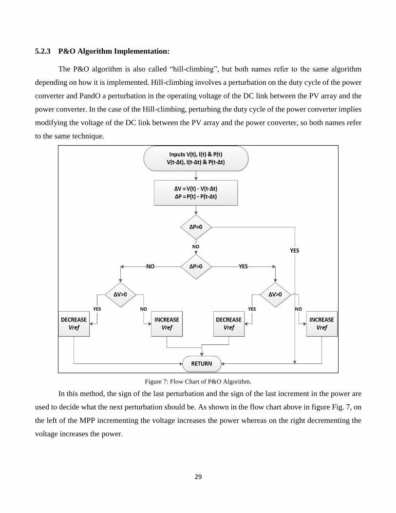
5.2.3 P&O Algorithm Implementation:
The P&O algorithm is also called “hill-climbing”, but both names refer to the same algorithm
depending on how it is implemented. Hill-climbing involves a perturbation on the duty cycle of the power
converter and PandO a perturbation in the operating voltage of the DC link between the PV array and the
power converter. In the case of the Hill-climbing, perturbing the duty cycle of the power converter implies
modifying the voltage of the DC link between the PV array and the power converter, so both names refer
to the same technique.
Figure 7: Flow Chart of P&O Algorithm.
In this method, the sign of the last perturbation and the sign of the last increment in the power are
used to decide what the next perturbation should be. As shown in the flow chart above in figure Fig. 7, on
the left of the MPP incrementing the voltage increases the power whereas on the right decrementing the
voltage increases the power.

30
If there is an increment in the power, the perturbation should be kept in the same direction and if
the power decreases, then the next perturbation should be in the opposite direction. Based on these facts,
the algorithm is implemented. The process is repeated until the MPP is reached. Then the operating point
oscillates around the MPP. This problem is common also to the InCond method, as was mention earlier.
A scheme of the algorithm is shown in Figure Fig. 7. In both P and O and InCond schemes, how fast the
MPP is reached depends on the size of the increment of the reference voltage. The drawbacks of these
techniques are mainly two. The first and main one is that they can easily lose track of the MPP if the
irradiation changes rapidly. In case of step changes they track the MPP very well, because the change is
instantaneous and the curve does not keep on changing. However, when the irradiation changes following
a slope, the curve in which the algorithms are based changes continuously with the irradiation, so the
changes in the voltage and current are not only due to the perturbation of the voltage. As a consequence it
is not possible for the algorithms to determine whether the change in the power is due to its own voltage
increment or due to the change in the irradiation.
When a solar array is used at a source of power, it is necessary to use a maximum power point
tracker in ensure minimal energy loss. The maximum power point tracker is implemented to track the
maximum power point. This needs to be tracked since due to temperature and illumination the maximum
power point will be continuously moving on the I-V curve. In our design, we will implement a
Synchronous Buck-Converter and we incorporate MPPT Controller to it and study is carried out in
MATLAB-Simulink environment.
Studying the algorithm presented in figure Fig. 7 meticulously, a program is designed in
MATLAB-Simulink for the design of MPPT Controller and thus the Maximum Power Point is achieved
in the system. This system also includes the PV Array which is designed in Chapter No.2. The obtained
results are depicted in RESULTS AND DISCUSSION section.

31
CHAPTER 6
Results & Discussions

32
6.1 PV System:
In order to verify the proposed study of small scale PV system of 19.8 W is considered. This
section reveals the simulation results of PV array using the equations depicted in last section in
MATLAB/Simulink environment. In this section we will explore the characteristics of PV array with the
change in irradiance and temperature and we will observe the changes in output power and current.
Fig.8 depicts the variation of Module current with Module Voltage with the variation of irradiance
on the module at the constant temperature i.e. of 30oC.
Fig.8 I-V Characteristics at constant temperature.
Fig.9 depicts the variation of Module power with Module Voltage with the variation of irradiance
on the module at the constant temperature i.e. of 30oC.
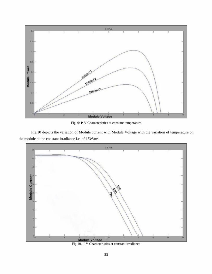
33
Fig .9: P-V Characteristics at constant temperature
Fig.10 depicts the variation of Module current with Module Voltage with the variation of temperature on
the module at the constant irradiance i.e. of 18W/m2.
Fig 10. I-V Characteristics at constant irradiance

34
Fig.11 depicts the variation of Module Power with Module Voltage with the variation of temperature on
the module at the constant irradiance i.e. of 18W/m2.
Fig.11. P-V Characteristics at constant irradiance
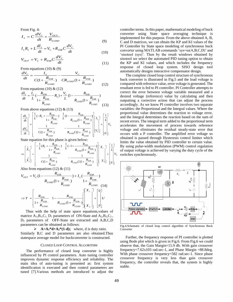
6.2 Closed Loop Bode Plot of Synchronous Buck Converter:
Fig.12.Bode plot of PI controller for Frequency Response
35
The frequency response of PI controller is plotted using Bode plot which is given in Fig.12. From
Fig.12 we could observe that, the Gain Margin=15.9 db. With gain crossover frequency=7.62x10³ rad.sec-
1, and Phase Margin =88.8deg. With phase crossover frequency=582 rad.sec-1. Since phase crossover
frequency is very less than gain crossover frequency, the controller reveals that, the system is highly stable.
6.3 Synchronous Buck Converter:
In order to verify the proposed study of small scale PV system of 19.8 W with dc-dc synchronous
buck converter module of is modeled and tested in MATLAB/Simulink environment. The parameters
taken for simulation study are given in the appendix. The performance of synchronous buck converter is
analyzed under different operating conditions and the corresponding results are presented here.
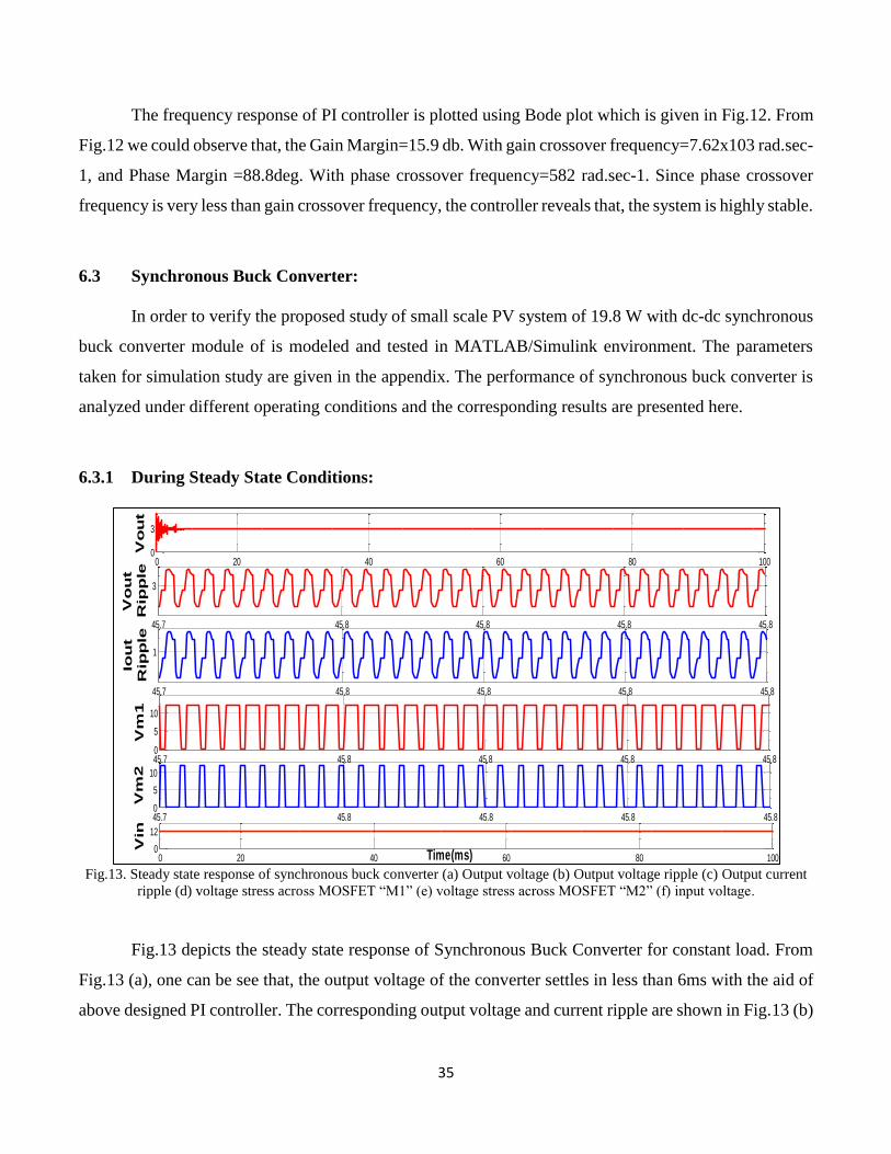
6.3.1 During Steady State Conditions:
Fig.13. Steady state response of synchronous buck converter (a) Output voltage (b) Output voltage ripple (c) Output current
ripple (d) voltage stress across MOSFET “M1” (e) voltage stress across MOSFET “M2” (f) input voltage.
Fig.13 depicts the steady state response of Synchronous Buck Converter for constant load. From
Fig.13 (a), one can be see that, the output voltage of the converter settles in less than 6ms with the aid of
above designed PI controller. The corresponding output voltage and current ripple are shown in Fig.13 (b)
0 100806040200
3
Vo
ut
45.8 45.845.7 45.845.8
3
Vo
ut
Rip
ple
45.845.8 45.8 45.845.7
1
Iou
t
Rip
ple
45.8 45.8 45.845.845.70
5
10
Vm
1
45.8 45.8 45.8 45.845.70
5
10
Vm
2
0 100806040200
12
Time(ms)
Vin

36
and Fig.13(c) respectively and the voltage and current ripple of output voltage which is maintained very
low with the help of the designed output capacitor which limits the output voltage and current ripple.
Voltage stress across MOSFET ‘M1’ & MOSFET ‘M2’are illustrated Fig.13(d) and Fig.13(e) with limited
values according to desired value. Fig.13(f) shows the response of input voltage from PV system which
maintains constant at 12V.
6.3.2 During Step Changes in Load:
Fig. 14. Response of synchronous buck converter during step changes in the load. (a) Response of Output voltage (b)
Settling of output voltage after change in load current. (c) Output voltage ripple (d) Output current ripple (e) Load Current
(f) voltage stress across MOSFET “M1” (g) voltage stress across MOSFET “M2”.
Fig.14 depicts the dynamic response of Synchronous Buck Converter during step changes in the
load. From Fig.14 (a), we could observe that, the output voltage settles less than 6ms and maintained
constant irrespective of the load variation from 1A to 1.5A as illustrated in Fig.14 (d) During load
variations, the transients in output voltage persist and it settles within 5ms from the evidence of Fig.14
(b). Voltage stress across MOSFET ‘M1’ & MOSFET ‘M2’are illustrated Fig.14 (d) and Fig.14 (e) with
limited values according to desired value. Fig.14 (f) shows the response of input voltage from PV system
which maintains constant at 12V.
0 50 100 150 200 250 3000
3
Vo
ut
99.5 100.3 101 101.7 102.4 103.1 103.8 104.6 105.3 106
2.95
3
3.05
Vo
ut
Settle
99.5 99.5 99.6 99.6 99.7 99.7 99.8 99.8
1
Iou
tR
ipp
le
0 50 100 150 200 250 3000.5
11.5
Iou
t
99.5 99.5 99.6 99.6 99.7 99.7 99.8 99.805
10
Vm
1
99.5 99.5 99.6 99.6 99.7 99.7 99.8 99.80
5
10
Time(ms)
Vm
2
99.5 99.5 99.6 99.6 99.7 99.7 99.8 99.8
3
Vo
ut
Rip
ple

37
6.3.3 During Variation of Solar irradiation and Temperature (Source Variation):
Fig. 15.Dynamics of Synchronous Buck Converter (a) Output voltage (b) Output voltage ripple (c) Output current ripple
(d) Solar Irradiation (f) Temperature (g) Output voltage of PV-Array i.e. input to Synchronous Buck Converter.
As illustrated in Fig.15, the source variation is considered as PV is cell possessing highly non-
linear characteristics between Ipv and Vpv due to variation of insolation and temperature. For more realistic
study, solar irradiation and temperature is measured at NIT, Rourkela campus from 12 P.M to 3 P.M and
are shown in Fig.15 (d) and Fig.15 (e) respectively. Due to variation on these parameters, Vpv is also
getting varied and is depicted in Fig.15 (e). During this source variation, the controller can able to improve
the dynamic response and it maintains the output voltage constant at 3 V and is shown in Fig.15 (a)
Fig.15(b) & Fig.15(c) depicts that the output voltage ripple and output current ripple are limited to very
less values by the help of high output capacitance.
6.4 Efficiency Comparison:
Fig.16 represents the efficiency comparison between two basic buck converter topologies.
Since, voltage drop against MOSFET M2 is lower than the voltage drop across diode in buck converter
topology. So, synchronous buck converter has low or less power dissipations and higher efficiency is
obtained. From the figure it’s evident that, Synchronous Buck Converter has better efficiency than
Conventional Buck Converter. The efficiency of synchronous buck converter at light load is higher than
0.65 0.65 0.65 0.65 0.65 0.65 0.65 0.65 0.65
1
Iou
tR
ipp
le
0 0.5 1 1.5 2 2.5 310
15
20
Irrad
ian
ce
(W/m
2)
0 0.5 1 1.5 2 2.5 320
40
50
Te
mp
(C)
0 0.5 1 1.5 2 2.5 38
9
10
11
12
Time(Sec.)
Vin
0 0.5 1 1.5 2 2.5 30
3
5V
ou
t
0.65 0.65 0.65 0.65 0.65 0.65 0.65 0.65 0.652.9998
3
3.0002
Vo
ut
Rip
ple

38
non-synchronous buck converter. However, under higher load level, the efficiency also depends on duty
cycle. However the tradeoff for better efficiency in Synchronous Buck Converter is the price of additional
MOSFET used. And also MOSFET saves space but complexity of control is increased because both
switches should not conduct simultaneously. (Any simultaneous conduction could cause to overload and
damage the system called as “shoot through”. To get rid of this a suitable delay called “dead-time” must
be incorporated.)
Fig. 16. Efficiency Comparison between Synchronous Buck Converter &
Conventional Buck Converter.
6.5 Maximum PowerPoint Tracking:
MPPT technique (P&O Algorithm) is implemented i.e perturbation on the duty cycle of the
power converter and a perturbation in the operating voltage of the DC link between the PV array and the
power converter is done so that maximum power is extracted from PV panel. As illustrated in Fig.17, PV
is cell possessing highly non-linear characteristics between Ipv and Vpv due to variation of insolation and
temperature. Fig.17 (d) and Fig.17 (e) indicates variation of solar irradiation and temperature respectively.
Due to variation on these parameters, Vpv is also getting varied and is depicted in Fig.17 (c). Converter
dynamic response is observed and it is seen that output voltage is maintained constant at 3 V and is shown
in Fig.17 (b) and Fig.17 (a) indicates load current.
1 2 3 4 5 6 7 8 9 1065
70
75
80
85
90
95
100
output power(in watts)
effic
ienc
y(in
%)
synchronous buck converter
buck converter

39
Fig.17 Response of Synchronous Buck Converter using MPPT technique (a) Output current (b) Output voltage (c) output
voltage of PV-Array i.e. input to Synchronous Buck Converter. (d)Solar Irradiation (e) Temperature
6.6 EXPERIMENTAL RESULTS:
As discussed in Chapter No.3, various components of Synchronous Buck Converter are designed and
bought through stores. The catalogue of items are given below:
Ready-made Inductor of value around 40μH.
Input Capacitor of value 100μF
Output Capacitor of value 500μ
Two N-Channel MOSFETS i.e. SiHG20N50C
Two resistors of 1.5Ω each.
High Voltage and High Speed power MOSFET or IGBT driver IR2213
As shown in the figure Fig. 18, experimental set up in laboratory is going to require Voltage
Source, CRO, Bread Boards, Connecting probes, Function generator etc., to carry out the experimental
work intended.
We operate at 170 kHz and we use a duty cycle of 50% for flexible operation of the
MOSFETs
0 0.5 1 1.50
1Iout
0 0.5 1 1.50
3Vout
0 0.5 1 1.510
12
Vin
0 0.5 1 1.510
15
20
Irradia
nce
0 0.5 1 1.520
40
60
Time(sec)
Tem
perature
40
Figure 18: Experimental Set-up in Laboratory
6.6.1 Conventional Buck converter:
Converter Input voltage shown in figure Fig. 19 is given through voltage source for
conventional buck converter set-up. With the help of CRO we can observe the obtained output voltage
which is shown in the figure Fig. 20, which concurs with the theoretical calculations of Buck Converter.
Figure 19: Input Voltage to Buck Converter
41
Figure 20: Output Voltage of Buck Converter
Figure 21: Voltage Across MOSFET
In the above figure Fig. 21 we can observe the voltage stress across the power MOSFET.

42
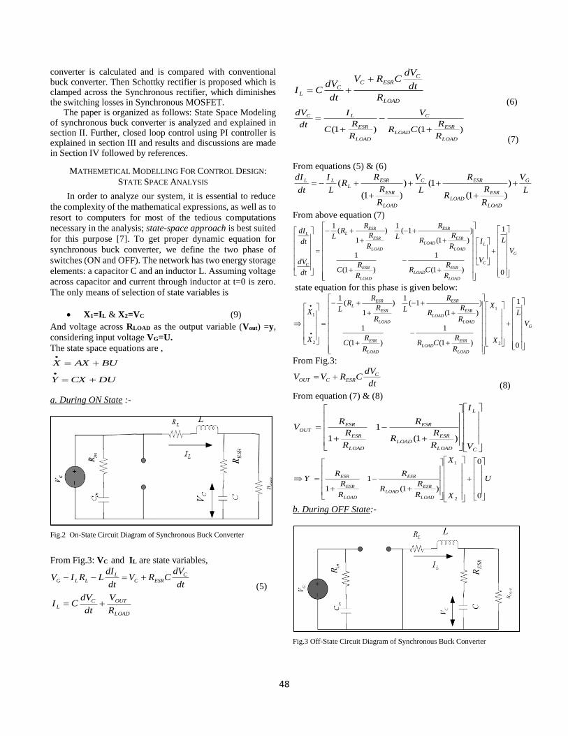
6.6.2 Synchronous Buck Converter:
Input voltage same as given to Buck Converter as shown in figure Fig. 19 is given through
voltage source for Synchronous buck converter set-up. With the help of CRO we can observe the obtained
output voltage which is shown in the figure Fig. 22, which concurs with the theoretical calculations of
Buck Converter. In figures Fig. 23 and Fig. 24 we can observe the voltage stress across the main MOSFET
and Synchronous MOSFET respectively.
From the figures, Fig. 22 and Fig. 20 it is evident that the output voltages for both
Conventional Buck Converter and Synchronous Buck Converter are identical for a given duty cycle.
However, as studied theoretically there will be a great deal of difference in the efficiencies in the
comparison of both converters, in which Synchronous Buck Converter have more efficiency than
Conventional Buck Converter as shown in the figure
Figure 22: Output Voltage for Synchronous Buck Converter
43
.
Figure 23: Voltage Across Main MOSFET M1
Figure 24: Voltage Across Synchronous MOSFET M2

44
CONCLUSIONS
In this project, an accurate mathematical modeling and design of synchronous buck
converter for low power PV energy system is presented. As solar array is used as a source of power, it is
necessary to use a maximum power point tracker to ensure minimal energy loss. The maximum power
point tracker is implemented to track the maximum power point in our synchronous buck conveter design.
The core idea of paper is to use State Space Averaging technique for modeling of converter which decides
precise values for PI controller used in control circuit. Synchronous buck converter with closed loop PI
controller precisely improved the dynamic response of the system during load as well as source variation
with reduced voltage and current ripple. Moreover, the circuit structure is simpler and much cheaper
compared to other control mechanisms where large number of components is needed. Further, the
converter design and its efficiency also determined. As results, the efficiency of synchronous buck
converter is higher than conventional dc-dc buck converter for same power rating. And the results obtained
from the experimental set up, satisfies with the simulation results.

45
REFERENCES
[1] J. Benner and L. Kazmerski, “Photovoltaic gaining greater visibility,” IEEE Spectrum., vol. 29,
pp. 34–42, Sep. 1999.
[2] B. Chitti Babu, S. Samantaray, N. Saraogi, M. Ashwin Kumar, R. Sriharsha, and S.
Karmaker, “Synchronous buck converter based pv energy system for portable applications,”
Proc. of IEEE Students’ Technology Symposium-2011.
[3] J.P.Lee, B. Min, T. Kim, D.W.Yoo, and J.Y.Yoo, “Design and control of novel topology for
photo-voltaic dc/dc converter with high efficiency under wide load ranges,” Journal of Power
Electronics., vol. 9, pp. 300–307, Mar., 2009.
[4] Tseng, Ching-Jung, and C.-L. Chen, “Novel zvt-pwm converters with active snubbers,” IEEE
Transactions On Power Electronics,, vol. 861-869, pp. 1005–1010, Sep. 1998.
[5] H. Altas and A. M. Sharaf, “A photovoltaic array simulation model for Matlab/Simulink GUI
environment,” Proc. Of International Conference on Clean Electrical Power, ICCEP’ 07,
May 21-23, 2007.
[6] S. Rahman, M. Khallat, and B. Chowdhury, “A discussion on the diversity in the applications of
photo-voltaic system,” IEEE Trans., Energy Conversion,, vol. 3, pp. 738– 746, Dec. 1988.
[7] F.Blaabjerg, Z. Chen, and S. B. Kjaer, “Power electronics as efficient interface in dispersed
power generation systems,” IEEE Trans., Power Electronics,, vol. 19, pp. 1184–1194, Sep.
2004.
[8] M.Nagao and K. Harada, “Power flow of photovoltaic system using buck-boost pwm power
inverter,,” Proc. Of IEEE International Conference on Power Electronics and Drives System.
PEDS,, vol. 1, pp. 144–149, 1997.
[9] E.Achille, T. Martir, C. Glaize, and C. Joubert, “Optimized dc-ac boost converters for
modular photo-voltaic grid-connected generators,” Proc. IEEE ISIE, pp. 1005–1010, 2004.
[10] S.M.Cuk, “Analysis and control of synchronous buck converter,” M.S, Thesis, 2009, Baskent
University, Turkey.

46
PAPERS PUBLISHED:
1. Suman Gunda, B.V.S.Pavan Kumar, M.Sagar Kumar, B.Chitti Babu, K.R.Subhashini “Modeling,
Analysis and Design of Synchronous Buck Converter using State Space Averaging
Technique for PV Energy System”, ISED-Conference 2012.

47
Modeling, Analysis and Design of Synchronous Buck Converter using State Space
Averaging Technique for PV Energy System
Gunda Suman, B.V.S.Pavan Kumar, M.Sagar Kumar, B.Chitti Babu, K.R.Subhashini Department of Electrical Engineering, National Institute of Technology, Rourkela-769 008
E-mail: [email protected], [email protected], [email protected], [email protected] ,
Abstract— Abstract-- In this paper, modeling, analysis and
design of synchronous buck converter for low power photo-
voltaic (PV) energy system is presented. For analyzing the
performance such converter, first we studied the characteristics
of PV array under different values of irradiance and
temperature. Then the exquisite design of Synchronous Buck
Converter with the application of State Space Modeling to
implement precise control design for the converter is presented.
The synchronous Buck Converter thus designed is used for
portable appliances such as mobiles, laptops, iPod’s laptops,
chargers, etc. In addition to that, closed loop control of
synchronous buck converter is studied in order to meet the
dynamic energy requirement of load especially during variation
of source i.e. variation of solar irradiation and temperature.
Further, the efficiency of synchronous buck converter is
calculated and is compared with conventional buck converter.
The studied model of complete system is simulated in the
MATLAB/Simulink environment and the results are obtained
with closeness to the theoretical study.
Keywords- PV Array, State Space Averaging, Synchronous
Buck Converter, portable applications, PI controller.
INTRODUCTION
At present scenario, the demand of energy is increasing exponentially and on the contrary the fossil fuel used for power generation is depleting. Also fossil fuel based power generation system causes the problem to the environment due to global warming and greenhouse effect. For clean and green energy generation, renewable energy sources such as wind, solar, micro-hydro power generating systems are playing a pivotal role for future energy demand. Hydro Energy generation and Wind Energy generation are of course two of the main sources of renewable energies, but the main disadvantage in Hydro Energy is that, it is seasonal dependent and in Wind energy is that it is geographical location dependent[1]. On the other hand Solar Energy is prevalent all over the globe and all the time. The amount of irradiance and temperature may vary from place to place and from time to time but under given conditions Solar Energy system can be implemented. Solar Energy or PV energy system is the most direct way to convert the solar radiation into electricity based on photovoltaic effect. Despite of high initial costs, they are already have been implemented in many rural areas. In future the cost of the PV panel also may diminish, because of the advancing material technology and also the competition between manufacturers. Thus PV energy system is mainly employed for small scale standalone systems or portable applications. The typical PV system feeds power to the load via power electronics converters is shown in Fig.1.
Fig. 1 Schematic Diagram of PV Based Converter System
The output voltage thus obtained from the PV panel is
DC. For low power applications, dc-dc converters are employed to step-up or step-down the output DC voltage according to the load requirements. However overall conversion efficiency is very low (typically 6.5%) So accurate modeling and design of dc-dc converter is necessary in order to improve the overall system performance with cost effective solution [2]. Various converter topologies have been proposed in the available literature [3]-[5]. In the conventional buck converter usually switching losses are high due to high switching frequency operation of MOSFET and losses in freewheeling diode is more due to larger forward voltage drop and consequently the overall efficiency is degraded to a great extent. The Synchronous Buck Converter proposed in [4] has an exquisite design with different modes of operation and with excellent response, but the design is very complex and more elements are involved in the circuit and as a result the solution is not cost effective. In the converter [5], where a keen design of PID Controller is proposed and implemented, it doesn’t depict the source dynamics of the converter during source variations. The converter in [6] is real time implemented in FPGA environment, but the overall efficiency of the converter is not discussed. So far many mathematical models for designing the control circuit for converters were presented but nowhere the splendid and simple design and interfacing of practical PV System with Synchronous Buck Converter was discussed.
This paper presents modeling and analysis of Synchronous Buck Converter for low power PV energy system application. The converter is modeled using state space averaging technique with simple mathematical equations. For achieving precise dynamic results, PI Controller is designed for which State Space Modeling procedure is presented to compute the Kp and KI values of controller. Further, the efficiency of synchronous buck
48
converter is calculated and is compared with conventional buck converter. Then Schottky rectifier is proposed which is clamped across the Synchronous rectifier, which diminishes the switching losses in Synchronous MOSFET.
The paper is organized as follows: State Space Modeling of synchronous buck converter is analyzed and explained in section II. Further, closed loop control using PI controller is explained in section III and results and discussions are made in Section IV followed by references.
MATHEMETICAL MODELLING FOR CONTROL DESIGN:
STATE SPACE ANALYSIS
In order to analyze our system, it is essential to reduce
the complexity of the mathematical expressions, as well as to
resort to computers for most of the tedious computations
necessary in the analysis; state-space approach is best suited
for this purpose [7]. To get proper dynamic equation for
synchronous buck converter, we define the two phase of
switches (ON and OFF). The network has two energy storage
elements: a capacitor C and an inductor L. Assuming voltage
across capacitor and current through inductor at t=0 is zero.
The only means of selection of state variables is
X1=IL & X2=VC (9)
And voltage across RLOAD as the output variable (Vout) =y,
considering input voltage VG=U.
The state space equations are ,
DUCXY
BUAXX
a. During ON State :-
Fig.2 On-State Circuit Diagram of Synchronous Buck Converter
From Fig.3: VC and IL are state variables,
dt
dVCRV
dt
dILRIV C
ESRCL
LLG (5)
LOAD
OUTCL
R
V
dt
dVCI
LOAD
CESRC
CL
R
dt
dVCRV
dt
dVCI
(6)
)1()1(LOAD
ESRLOAD
C
LOAD
ESR
LC
R
RCR
V
R
RC
I
dt
dV
(7)
From equations (5) & (6)
L
V
R
RR
R
L
V
R
R
RR
L
I
dt
dI G
LOAD
ESR
LOAD
ESRC
LOAD
ESR
ESR
L
LL
)
)1(
1()
)1(
(
From above equation (7)
G
C
L
LOAD
ESRLOAD
LOAD
ESR
LOAD
ESRLOAD
ESR
LOAD
ESR
ESRL
C
L
V
L
V
I
R
RCR
R
RC
R
RR
R
L
R
R
RR
L
dt
dV
dt
dI
0
1
)1(
1
)1(
1
)
)1(
1(1
)
1
(1
state equation for this phase is given below:
G
LOAD
ESRLOAD
LOAD
ESR
LOAD
ESRLOAD
ESR
LOAD
ESR
ESRL
V
L
X
X
R
RCR
R
RC
R
RR
R
L
R
R
RR
L
X
X
0
1
)1(
1
)1(
1
)
)1(
1(1
)
1
(1
2
1
2
1
From Fig.3:
dt
dVCRVV C
ESRCOUT (8)
From equation (7) & (8)
C
L
LOAD
ESRLOAD
ESR
LOAD
ESR
ESROUT
V
I
R
RR
R
R
R
RV
)1(
1
1
U
X
X
R
RR
R
R
R
RY
LOAD
ESRLOAD
ESR
LOAD
ESR
ESR
0
0
)1(
1
1
2
1
b. During OFF State:-
Fig.3 Off-State Circuit Diagram of Synchronous Buck Converter
49
From Fig. 4:
LOAD
OUTCL
R
V
dt
dVCI
(9)
dt
dVCRV
dt
dILRI C
ESRCL
LL (10)
dt
dVCRVV C
ESRCOUT (11)
From equations (10) & (9)
)1()1(LOAD
ESRLOAD
C
LOAD
ESR
LC
R
RCR
V
R
RC
I
dt
dV
(12)
From equations (10) & (12)
)
)1(
1()
1
(
LOAD
ESRLOAD
ESRCL
LOAD
ESR
ESRLL
R
RR
R
L
VR
R
R
R
L
I
dt
dI
(13)
From above equations (12) & (13)
G
C
L
LOAD
ESRLOAD
LOAD
ESR
LOAD
ESRLOAD
ESR
LOAD
ESR
ESRL
C
L
V
L
V
I
R
RCR
R
RC
R
RR
R
L
R
R
RR
L
dt
dV
dt
dI
0
1
)1(
1
)1(
1
)
)1(
1(1
)
1
(1
State equation for this phase is given below:
G
LOAD
ESRLOAD
LOAD
ESR
LOAD
ESRLOAD
ESR
LOAD
ESR
ESRL
V
L
X
X
R
RCR
R
RC
R
RR
R
L
R
R
RR
L
X
X
0
1
)1(
1
)1(
1
)
)1(
1(1
)
1
(1
2
1
2
1
Also from equations (12) & (11)
)
1
()
)1(
1(
LOAD
ESR
ESRL
LOAD
ESRLOAD
ESRCOUT
R
R
RI
R
RR
RVV
(14)
U
X
X
R
RR
R
R
R
RY
LOAD
ESRLOAD
ESR
LOAD
ESR
ESR
0
0
)1(
1
1
2
1
Thus with the help of state space equations,values of
matrice A1,B1,C1, D1 parameters of ON-State and A2,B2,C2 ,
D2 parameters of OFF-State are extracted and A,B,C,D
parameters can be obtained as follows:
A=A1*d+A2*(1-d); where, d is duty ratio.
Similarly B,C and D parameters are also obtained.Thus
statespace average model for buckconverter is constructed.
CLOSED LOOP CONTROL ALGORITHM
The performance of closed loop converter is highly influenced by PI control parameters. Auto tuning controller improves dynamic response efficiency and reliability. The main idea of auto-tuning is presented as: first system identification is executed and then control parameters are tuned [7].Various methods are introduced to adjust the
controller terms. In this paper, mathematical modeling of buck converter using State space averaging technique is implemented for this purpose. From the above obtained A, B, C and D matrices, we can obtain the KP and KI values of the PI Controller by State space modeling of synchronous buck converter using MATLAB commands ‘sys=ss(A,B,C,D)’ and ‘sisotool (sys)’. Then by the result windows obtained by sisotool we select the automated PID tuning option to obtain the KP and KI values, and which includes the frequency response of closed loop system. SISO design tool automatically designs interactive compensator design.
The complete closed loop control structure of synchronous buck converter is illustrated in Fig.5 and the load voltage is compared with reference value, error voltage is generated. The resultant error is fed to PI controller. PI Controller attempts to correct the error between voltage variable measured and a desired voltage (reference) value by calculating and then outputting a corrective action that can adjust the process accordingly. As we know PI controller involves two separate variables: the Proportional and the Integral values. Where the proportional value determines the reaction to voltage error, and the Integral determines the reaction based on the sum of recent errors. The integral term added to the proportional term accelerates the movement of process towards reference voltage and eliminates the residual steady-state error that occurs with a P controller. The amplified error voltage so obtained is passed through Hysteresis control limiter which limits the value obtained by PID controller to certain value. By using pulse-width modulation (PWM) control regulation of output voltage is achieved by varying the duty cycle of the switches synchronously.
Fig.4.Schematic of closed loop control algorithm of Synchronous Buck Converter
Further, the frequency response of PI controller is plotted
using Bode plot which is given in Fig.6. From Fig.6 we could observe that, the Gain Margin=15.9 db. With gain crossover frequency=7.62x10³ rad.sec-1, and Phase Margin =88.8deg. With phase crossover frequency=582 rad.sec-1. Since phase crossover frequency is very less than gain crossover frequency, the controller reveals that, the system is highly stable.

50
Fig.5.Bode plot of PI controller for Frequency Response.
SIMULATION RESULTS AND DISCUSSION
In order to verify the proposed study of small scale PV system of 19.8 W with dc-dc synchronous buck converter module of is modeled and tested in MATLAB/Simulink environment. The parameters taken for simulation study are given in the appendix. The performance of synchronous buck converter is analyzed under different operating conditions and the corresponding results are presented here.
During Step Changes in the Load:
Fig. 8. Response of synchronous buck converter during step changes in the load. (a) Response of Output voltage (b) Settling of output voltage after
change in load current. (c) output voltage ripple (d)output current ripple (e)
Load Current (f) voltage stress across MOSFET “M1” (g) voltage stress across MOSFET “M2” .
Fig.8 depicts the dynamic response of Synchronous Buck
Converter during step changes in the load. From Fig.2.2 (a),
we could observe that, the output voltage settles less than 6ms
and maintained constant irrespective of the load variation
from 1A to 1.5A as illustrated in Fig.8(d) During load
variations, the transients in output voltage persist and it
settles within 5ms from the evidence of
Fig.8.(b). Voltage stress across MOSFET ‘M1’ &
MOSFET ‘M2’are illustrated Fig.7 (d) and Fig.7 (e) with
limited values according to desired value. Fig.7 (f) shows the
response of input voltage from PV system which maintains
constant at 12V.
During Variation of Solar irradiation and Temperature
(Source Variation):
Fig. 9.Dynamics of Synchronous Buck Converter (a) ouput voltage (b)
output voltage ripple (c)output current ripple (d)Solar Irradiation (f)
Temperature (g)output voltage of PV-Array i.e. input to Synchronous Buck Converter.
As illustrated in Fig.9, the source variation is considered
as PV is cell possessing highly non-linear characteristics
between Ipv and Vpv due to variation of insolation and
temperature. For more realistic study, solar irradiation and
temperature is measured at NIT, Rourkela campus from 12
P.M to 3 P.M and are shown in Fig.9.(d) and Fig.9.(e)
respectively. Due to variation on these parameters, Vpv is
also getting varied and is depicted in Fig.9 (e). During this
source variation, the controller can able to improve the
dynamic response and it maintains the output voltage
constant at 3 V and is shown in Fig.9 (a). Fig.9(b) & Fig.9(c)
depicts that the output voltage ripple and output current ripple
are limited to very less values by the help of high output
capacitance.
Converter Design and Its Efficiency Calculation:
The following interpretations are made for capacitor and
inductor calculation.
a) Inductance Calculation
For an inductor, V=L*ΔI/ΔT
Rearrange and substitute:
L = (Vin – Vout)*(D / Fsw )/Iripple
b) Output Capacitor Calculation
For a capacitor, ΔV=ΔI*(ESR+ΔT/C + ESL/ΔT)
Assume ripple voltage of 50 mV
Then, Cout= (ΔI*ΔT)/ (ΔV-(ΔI*ESR) =10.71μF
0 50 100 150 200 250 3000
3
Vo
ut
99.5 100.3 101 101.7 102.4 103.1 103.8 104.6 105.3 106
2.95
3
3.05
Vo
ut
Settle
99.5 99.5 99.6 99.6 99.7 99.7 99.8 99.8
1
Io
ut
Rip
ple
0 50 100 150 200 250 3000.5
11.5
Io
ut
99.5 99.5 99.6 99.6 99.7 99.7 99.8 99.805
10
Vm
1
99.5 99.5 99.6 99.6 99.7 99.7 99.8 99.80
5
10
Time(ms)
Vm
2
99.5 99.5 99.6 99.6 99.7 99.7 99.8 99.8
3
Vo
ut
Rip
ple
0.65 0.65 0.65 0.65 0.65 0.65 0.65 0.65 0.65
1
Iou
tR
ipp
le
0 0.5 1 1.5 2 2.5 310
15
20
Irrad
ian
ce
(W
/m2)
0 0.5 1 1.5 2 2.5 320
40
50
Te
mp
(C
)
0 0.5 1 1.5 2 2.5 38
9
10
11
12
Time(Sec.)V
in
0 0.5 1 1.5 2 2.5 30
3
5
Vo
ut
0.65 0.65 0.65 0.65 0.65 0.65 0.65 0.65 0.652.9998
3
3.0002
Vo
ut
Rip
ple
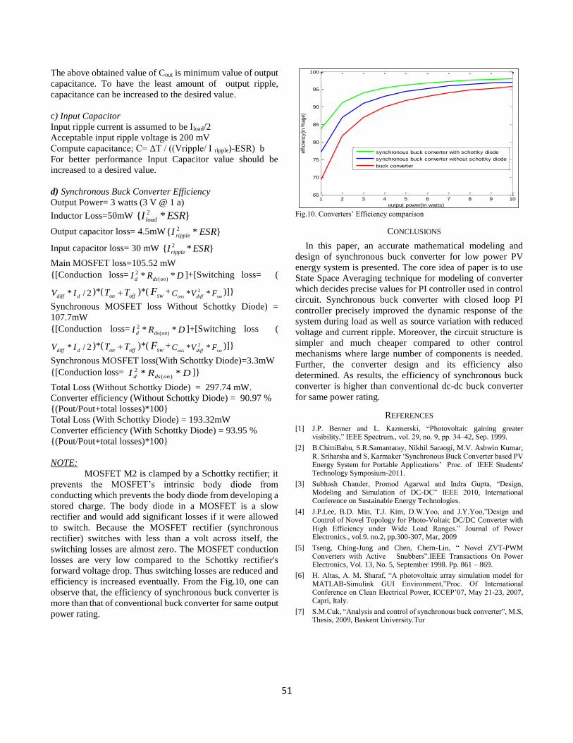
51
The above obtained value of Cout is minimum value of output
capacitance. To have the least amount of output ripple,
capacitance can be increased to the desired value.
c) Input Capacitor
Input ripple current is assumed to be Iload/2
Acceptable input ripple voltage is 200 mV
Compute capacitance; C= ΔT / ((Vripple/ I ripple)-ESR) b
For better performance Input Capacitor value should be
increased to a desired value.
d) Synchronous Buck Converter Efficiency
Output Power= 3 watts (3 V @ 1 a)
Inductor Loss=50mW }*{ 2 ESRI load
Output capacitor loss= 4.5mW }*{ 2 ESRI ripple
Input capacitor loss= 30 mW }*{ 2 ESRI ripple
Main MOSFET loss=105.52 mW
{[Conduction loss= DRI ondsd ** )(
2 ]+[Switching loss= (
2/* ddiff IV )*(offon TT )*(
swF +swdiffoss FVC ** 2 )]}
Synchronous MOSFET loss Without Schottky Diode) =
107.7mW
{[Conduction loss= DRI ondsd ** )(
2 ]+[Switching loss (
2/* ddiff IV )*(offon TT )*(
swF +swdiffoss FVC ** 2 )]}
Synchronous MOSFET loss(With Schottky Diode)=3.3mW
{[Conduction loss= DRI ondsd ** )(
2 ]}
Total Loss (Without Schottky Diode) = 297.74 mW.
Converter efficiency (Without Schottky Diode) = 90.97 %
{(Pout/Pout+total losses)*100}
Total Loss (With Schottky Diode) = 193.32mW
Converter efficiency (With Schottky Diode) = 93.95 %
{(Pout/Pout+total losses)*100}
NOTE:
MOSFET M2 is clamped by a Schottky rectifier; it
prevents the MOSFET’s intrinsic body diode from
conducting which prevents the body diode from developing a
stored charge. The body diode in a MOSFET is a slow
rectifier and would add significant losses if it were allowed
to switch. Because the MOSFET rectifier (synchronous
rectifier) switches with less than a volt across itself, the
switching losses are almost zero. The MOSFET conduction
losses are very low compared to the Schottky rectifier's
forward voltage drop. Thus switching losses are reduced and
efficiency is increased eventually. From the Fig.10, one can
observe that, the efficiency of synchronous buck converter is
more than that of conventional buck converter for same output
power rating.
Fig.10. Converters’ Efficiency comparison
CONCLUSIONS
In this paper, an accurate mathematical modeling and
design of synchronous buck converter for low power PV
energy system is presented. The core idea of paper is to use
State Space Averaging technique for modeling of converter
which decides precise values for PI controller used in control
circuit. Synchronous buck converter with closed loop PI
controller precisely improved the dynamic response of the
system during load as well as source variation with reduced
voltage and current ripple. Moreover, the circuit structure is
simpler and much cheaper compared to other control
mechanisms where large number of components is needed.
Further, the converter design and its efficiency also
determined. As results, the efficiency of synchronous buck
converter is higher than conventional dc-dc buck converter
for same power rating.
REFERENCES
[1] J.P. Benner and L. Kazmerski, “Photovoltaic gaining greater visibility,” IEEE Spectrum., vol. 29, no. 9, pp. 34–42, Sep. 1999.
[2] B.ChittiBabu, S.R.Samantaray, Nikhil Saraogi, M.V. Ashwin Kumar, R. Sriharsha and S, Karmaker ‘Synchronous Buck Converter based PV Energy System for Portable Applications’ Proc. of IEEE Students' Technology Symposium-2011.
[3] Subhash Chander, Promod Agarwal and Indra Gupta, “Design, Modeling and Simulation of DC-DC” IEEE 2010, International Conference on Sustainable Energy Technologies.
[4] J.P.Lee, B.D. Min, T.J. Kim, D.W.Yoo, and J.Y.Yoo,”Design and Control of Novel Topology for Photo-Voltaic DC/DC Converter with High Efficiency under Wide Load Ranges.” Journal of Power Electronics., vol.9. no.2, pp.300-307, Mar, 2009
[5] Tseng, Ching-Jung and Chen, Chern-Lin, “ Novel ZVT-PWM Converters with Active Snubbers”.IEEE Transactions On Power Electronics, Vol. 13, No. 5, September 1998. Pp. 861 – 869.
[6] H. Altas, A. M. Sharaf, “A photovoltaic array simulation model for MATLAB-Simulink GUI Environment,”Proc. Of International Conference on Clean Electrical Power, ICCEP’07, May 21-23, 2007, Capri, Italy.
[7] S.M.Cuk, “Analysis and control of synchronous buck converter”, M.S, Thesis, 2009, Baskent University.Tur
1 2 3 4 5 6 7 8 9 1065
70
75
80
85
90
95
100
effic
ienc
y(in
%ag
e)
output power(in watts)
synchronous buck converter with schottky diode
synchronous buck converter without schottky diode
buck converter

52