modeling of the contact between the metal tip and n-type semiconductor as a schottky ... ·...
TRANSCRIPT

Modeling of the Contact between the Metal Tip and n-type Semiconductor as aSchottky Barrier and Tunneling Current Calculation
Dongwook Go∗
Institute of Solid State Physics, Technical University of Graz, Petersgasse 16, 8010 Graz, Austria(Dated: February 3, 2013)
The contact between the metal tip and n-type semiconductor contact is modeled as a Schottkybarrier and IV curves are calculated for various parameters. It is observed that when the thermioniccurrent dominates the tunneling current contribution (high T , large a, small U0, large ξ) the IVcurve just follows the usual diode behavior. However, when tunneling current dominates (low T ,small a, large U0, small ξ), the reverse current starts to appear and thereby reverse the rectifyingbehavior of the diode.
INTRODUCTION
FIG. 1. Four-point measurement is widely used to mea-sure the resistivity of the sample. (Source : http://lamp.tu-graz.ac.at/ hadley/sem/index/index.php)[1]
Nowadays, electron devices tend to have small sizes (afew nanometers to a few microns). In order to investigatethe small size devices, in TU Graz, a scanning electronmicroscope (SEM) is used with a sharp metal tip whichcan move accurately within a few nanometers[1]. Withthe sharp metal tip, the current and the voltage are mea-sured. For example, the resistivity of the sample can bemeasured through the four-point measurement (Fig.1).Also, the electron beam induced current (EBIC) methodis commonly used to identify buried junctions or defectsin semiconductors, or to examine minority carrier prop-erties (Fig.2). As mentioned above, many experimentsdepend on the tip measurement, so it is important tounderstand the contact between the tip and the sample.
However, little is known about the properties of thecontact between the tip and the sample although manyexperiments depend on the tip measurement, so the re-search on the properties of the contact has to be done. Intwo-point measurement of the IV curve, most of the re-sistance comes from the contact, and the IV curve showsthat the resistivity becomes smaller as the bias voltageincreases for both forward and reverse bias voltages. To
FIG. 2. EBIC method is used to study buried junctionsor defects in semiconductors. (Source : http://lamp.tu-graz.ac.at/ hadley/sem/index/index.php)[1]
explain the shape of the IV curve, the theoretical modelis suggested in this paper and the IV characteristic isexplained with the suggested model.
In the theoretical model, Schottky contact is formed atthe contact between the metal tip and the n-type semi-conductor sample. Assuming that the charge density isconstant through the depletion layer, the potential bar-rier can be calculated, which shows a V ∼ r−1 behavior.Then, the Schrodinger equation is solved with the calcu-lated potential function. In this step, the transmissioncoefficient is obtained. Finally, the current density is cal-culated using the calculated transmission coefficient andthe Fermi-Dirac distribution function.
Meanwhile, to be sure about the calculation, the cur-rent density was calculated for the square barrier poten-tial, which agrees well with the previous study[2].
For the spherical shape Schottky barrier, the diode-likebehavior is observed when the thermionic current dom-inates the tunneling current, which can be understoodin general terms like in many other semiconductor text-books. However, when the tunneling current is a majorsource of the current, it is observed that the reverse cur-rent starts to appear, so the rectifying behavior of thediode is reversed.

2
THEORY AND MODEL
A. Modeling of the Contact : Spherical ShapeSchottky Barrier
FIG. 3. (a) Geometry of the contact between the tip and thesample. (b) The model is simplified to have a spherical shapecontact.
In the theoretical model, there is a metal tip, and thesample is assumed to be a n-type semiconductor. Theanalysis of a p-type semiconductor is almost the same asthe n-type one. The usual geometry of the tip measure-ment is like Fig.3. The tip and the n-type semiconduc-tor sample become contact each other, and the Schottkycontact is formed if the Fermi energy of the n-type semi-conductor is higher than that of metal tip. The electronmoves to the metal tip side, so the positively charged de-pletion region is formed around the tip. In the model, Iassumed for the mathematical simplicity that the shapeof the contact is spherical shape with a radius a.
In Fig.4, the energy level diagram of Schottky contactis illustrated[3]. Before the contact is formed, the Fermienergy of the n-type semiconductor is higher than thatof the metal tip. When the two become contact eachother, small amount of electron moves to the metal side,so the Fermi energies of both sides become equal andthe Schottky barrier is formed. When the bias voltage isapplied, the difference of the Fermi energies becomes eV .
B. Potential Barrier Calculation through thePoisson Equation
For the simplicity, I assumed that the charge densityat the depletion layer is constant (ρ = eNd), which iscalled the depletion approximation[4]. Then, the Poissonequation
∇2V (~r) = −ρε
(1)
is to be solved. Here, the electric potential is radiallysymmetric (V (~r) = V (r)), so the Poisson equation be-comes
1
r2d
dr
(r2d
drV (r)
)= −eNd
ε. (2)
FIG. 4. Before the contact is formed, Fermi energy ofthe n-type semiconductor is higher than that of metaltip. When the two become contact each other, smallamount of electron moves to the metal side, so the Fermienergies of both sides become equal and the Schottkybarrier is formed. When the bias voltage is applied,the difference of Fermi energies becomes eV . (Source :http://web.tiscali.it/decartes/phd html/node3.html)[3]
If we multiply r2 and integrate,
r2d
drV (r) = −eNdr
3
3ε+ C1 (3)
and, if we divide by r2 and integrate, we arrive at thegeneral form of the potential.
V (r) = −eNdr2
6ε− C1
r+ C2 (4)
The coefficient C1 can be obtained by using the factthat at the end of the depletion layer(r = rd) the electricfield vanishes,
E(rd) = − d
drdV (rd) = −eNdrd
3ε+C1
rd2(5)
so, C1 = eNdr3d/3ε. The coefficient C2 can be ob-
tained by setting the ground potential as V (rd) = 0, soC2 = 3Ndr
2d/2ε. Therefore, the electric potential of the
spherical Schottky contact is
V (r) =
Vbi (r < a)eNd
6ε
(3rd
2 − r2 − 2rd3
r
)(a ≤ r ≤ rd)
0 (r ≥ rd)(6)
with the constraint V (a) = Vs + Vbi, where Vs is theintrinsic potential drop at the contact, and Vbi is thebias voltage applied to the metal side.

3
FIG. 5. Potential energy (U = −eV ) profile for various Vbi
values. When negative(positive) voltage is applied the bar-rier becomes higher(lower) and thicker(thinner). The intrinsicvoltage drop (Vs) is set to −1 V .
FIG. 6. As the metal side becomes more negatively biased thedepletion layer radius (rd) increases. The intrinsic potentialdrop at the barrier (Vs) is set to be −1 V .
At Fig.6, potential energy profile for various bias volt-age (Vbi) is shown. When negative voltage is applied thebarrier becomes higher and thicker, and vice versa. Itwas assumed that Nd = 1015 cm−3, and a = 1nm. Also,at the Fig.5, the radius of the depletion layer (rd) is cal-culated for various bias voltages. It can be seen thatas the bias voltage becomes negative the depletion layerthickness increases.
C. Schrodinger Equation and TransmissionProbability
In general, the transmission probability can be calcu-lated by solving time-independent Schrodinger equation.
− h2
2m∗d2
dx2ψE(x) + U(x)ψE(x) = EψE(x) (7)
FIG. 7. Schematic diagram of the potential barrier and thetunneling phenomenon. When an incident wave (AIe
iklx) ap-proaches to the barrier, a part is reflected back (ARe
−iklx)and the other part transmits through the barrier (AT e
ikrx).
where m∗ is an effective mass of the electron.Suppose the system where the potential is constant
at a region x < 0 and x > a and in between there’s apotential barrier. Here, Ul(Ur) is a constant potential onleft(right) side.
U(x) =
Ul (x < 0)
Ubarrier(x) (0 < x < a)
Ur (x > a)
(8)
It is known that the solution under the constant po-tential is a plane wave. So we can write the solution asa combination of the incident wave, the reflected wave,and the transmitted wave
ψE(r) =
{AI(E)eiklx +AR(E)e−iklx (x < 0)
AT (E)eikrx (x > a)(9)
where
kl =
√2m∗(E − Ul)
h(10)
and
kr =
√2m∗(E − Ur)
h, (11)
which are the wave numbers on the left(right) side. Aschematic diagram is shown in Fig.(7).
With the initial condition{ψ(x = a) = eikrx(∂ψ∂x
)x=a
= ikreikrx
(12)
we can integrate the Eq.(7) numerically and get ψ anddψ/dx at the point x = 0. Here we can impose thecondition AT = 1 since only the relative values of co-efficients are physically meaningful. The coefficients are

4
FIG. 8. The periodic boundary condition assumes that thewave function is the same in every period L(� a).
just needed to meet the constraint, |AI |2 = |AR|2+|AT |2.Therefore, we can calculate AI and AT as follows.AI(E) = 1
2ψ(0) + 12ik
(∂ψ∂x
)x=0
AT (E) = 12ψ(0)− 1
2ik
(∂ψ∂x
)x=0
(13)
Then, we can calculate the transmission probability as
T (E) = 1−∣∣∣∣AR(E)
AI(E)
∣∣∣∣2 . (14)
D. Current Density
Current density can be calculated from the tunnelingprobability and the Fermi-Dirac distribution[4]. For theconvenience in counting the number of states, periodicboundary condition is imposed. The boundary conditionassumes that the wave function is same in every spaceperiod L, which means that the wave function has a pe-riod L. The period L is assumed to be much larger thanthe system itself (L� a).
Let’s consider the system in Fig.8. The incident wavecoming from the left side (AIe
ikx) is reflected (ARe−ikx)
and transmitted (AT eikx) at the potential barrier. If we
set AI = 1, the normalized wave function is given by
ψk(r) =
{1√L
(eikx +AR(k)e−ikx
)(left side)
1√LAT (k)eikx (right side)
. (15)
so when the boundary condition (ψk(x + L) = ψk(x))is imposed, the possible k values form a set of discretenumbers, and the unit length of k-space becomes 2π/L
k =2π
Lm, m ∈ Z (16)
where Z is the set of integers.The current density of the quantum state with the
wave number k is the electron charge (−e) times the
probability current.
Jk(L→ R) = − eh
2m∗i
[ψ∗k∂ψk∂x− ψk
∂ψ∗k∂x
]= (−e)T (k)
L
hk
m(17)
The overall current density of the left-incoming case issum over the all possible k values times Fermi functionfactor.
J(L→ R) = 2∑k
(−e)T (k)
L
hk
mfL(k) (1− fR(k)) (18)
where the first Fermi function factor (fL(k)) is the prob-ability that the state k is occupied on the left side of thebarrier, and the second factor (1 − fR(k)) is the proba-bility that the state k is empty on the right side of thebarrier. Meanwhile, the factor 2 in the front comes fromthe spin degree of freedom for each k values. If we changeit into the integral representation, it becomes
J(L→ R) =2
(2π/L)
∫k
dk(−e)T (k)
L
hk
mfL(k) (1− fR(k)) .
(19)The last step is to change the integral variable into theenergy, E = hk2/2m, and the integral becomes
J(L→ R) = −4e
h
∫E
T (E)fL(E)(1− fR(E))dE. (20)
Similarily, the current density which flows from the rightside to the left side is
J(R→ L) = −4e
h
∫E
T (E)fR(E)(1− fL(E))dE. (21)
Therefore the total current is the difference of the twocontributions.
Jtotal =4e
h
∫E
T (E)(fR(E)− fL(E))dE. (22)
EXPERIMENT AND RESULT
Experimental result was referred from Alexander Schn-abel and Stephan Stonica’s report of the class, experi-mental laboratory exercise, in TU Graz[4].
The setup for the experiment is shown in Fig.9. Apart of the n-doped silicon wafer is placed between thetwo copper plates. The sample was proton-doped siliconwafer produced by Infineonn named P570 530. Four tipsdriven by the macro manipulator are placed on the sili-con. All the tips and copper plates are enumerated from1 to 6. The tip 1,2, and 3 are composed of tungsten, and4 is copper-beryllium. The copper plates are enumeratedas 5 and 6.
A series of two-point measurements between the tipsor between the tip and the copper plates has been carriedout, and the IV curve is shown in Fig.10. It is observed

5
FIG. 9. Setup for the measurement. 1-3 Tungsten Tips, 4Copper-Beryllium tip, 5,6 Copper-plates.
FIG. 10. The IV curves for the tip-semiconductor con-tact.(blue : tip-tip, green : tip1-cu, red : tip2-cu, turquoise :red and green added) On the left side one tungsten and onecopper-beryllium tip is used, while two tungsten tips wereused in the right.
from the IV curve that the resistivity becomes smaller asthe magnitude of the bias voltage increases. In Fig.10-(a), the IV curve of 34 is compared with the sum of thetwo curves, 35+45, which gives almost the same result.This suggests that the most of the resistivity comes fromthe tip-semiconductor contact, and that the resistivitywhich comes from the contact between the copper plateand the semiconductor is small. The same thing can alsobe seen in Fig.10-(b).
Therefore, it is concluded that the resistivity thatcomes from the tip-semiconductor contact shows nonlin-ear behavior, where the resistivity becomes smaller asthe magnitude of the bias voltage increases. In the nextsection, the IV curve at the tip-semiconductor contactis numerically calculated, and this behavior is explainedwithin the theoretical model.
NUMERICAL CALCULATION RESULT
Using the theory and the model discussed before, theIV curves are calculated for both square and Schottkypotential barrier.
FIG. 11. Energy band diagram of the square potential barrierwhen (a) Vbi > 0 and (b) Vbi < 0.
A. Square Barrier
The parameters for the calculations are defined as be-low (See Fig.11) :
Barrier Height U0
Barrier Width aFermi Energy on the Left/Right EF,l/EF,rConduction Band Bottom on the Left/Right EC,l/EC,rEF − EC ξl/ξrBias Voltage Vbi
As the two different materials become contact eachother, the Fermi energies of two different materials be-come the same. Then, if a bias voltage is applied, theFermi energies becomes different as Eq.(25), so electronscan flow.
EF,r − EF,l = −eVbi (23)
Moreover, the wave vectors on the left and right sides aregiven by
kl =
√2mE
h2, (24)
and
kr =
√2m(E + ξl − ξr + eVbi)
h2, (25)
where E is the energy of the electron which is set to bezero at the bottom of the conduction band on the rightside.
The first thing to note is the dependence of the bar-rier thickness, a. In Fig.12, IV curves were calculated forthe barrier thicknesses 10−11 m, 10−10 m, 10−9 m, and10−8 m. The other conditions were set to be the same(U0 = 2 eV , ξl = ξr = 2 eV , T = 300 K). It can beseen that as the barrier thickness becomes smaller it be-comes to follow the Ohmic behavior while the curves havethe bigger curvature when the barrier becomes thick.When the barrier is thick it’s hard for electrons to pene-trate through the tunneling, so the electrons can tunnelthrough the barrier only when the high enough bias volt-age is applied .

6
FIG. 12. IV curves for various values of barrier thickness. Asthe barrier thickness become smaller it becomes to follow theOhmic behavior while the curves have bigger curvature whenthe barrier is thick.
FIG. 13. Temperature dependence of the IV curves. In ex-tremely high temperature the Ohmic behavior is observed.While in low temperature regime, the curvatures of the curvecan be seen, especially for the T = 3000 K case, which comesfrom the quantum interference effect.
In Fig.13, a similar trend can also be observed inthe calculation for various temperatures (30 K, 300 K,3000 K, and 30000 K) while all the other conditionswere set to be the same (U0 = 2 eV , ξl = ξr = 2 eV ,a = 1 nm). In extremely high temperature, the IV curvejust becomes linear, where the contribution to the currentcomes mostly from the thermionic emission. While in alow temperature region, like 30 K and 300 K, most of thecurrent comes from the tunneling electrons whose energyis low. An interesting behavior is observed at 3000 K,where the curvature can be seen easily. In this temper-ature region there are enough electrons whose energy isalmost at the tip of the barrier, so they can tunnel easily.
FIG. 14. IV curves for the different U0 values. It’s Ohmicwhen the height is small and come to have a curvature as theheight becomes bigger. Especially for the U0 = 0 case, thefunny shape of the curve can be observed since the energy ofthe electrons is almost at the edge of the barrier.
The electrons in this energy region show the quantum in-terference effect where incoming wave and reflected waveinterfere each other, thus showing a funny shape of theIV curve.
The next thing to note is the barrier height dependenceof the IV curves. In Fig.14, IV curves for various barrierheight are shown. Here also, the other conditions areset to be the same for each calculation (T = 300 K, ξl =ξr = 2 eV , a = 1 nm). The first case, U0 = −2 eV meansthe free space, no barrier case. When the barrier heightis low the IV curves are linear. As the barrier heightincreases, the IV curves come to have a curvature, andan interesting IV curve can be observed for the U0 = 0case where the electrons have an energy that is almostequal to the edge of the barrier, so the interference occurs.
Finally, the IV curves for various ξr values (0-4 eV)are shown in Fig.15. When ξr = 0 the current densitybecomes zero for the negative bias voltage since there isno electron to flow. As ξr increase, the IV curves becomemore symmetric. However, it can be observed that theshape of the IV curves does not change anymore whenξr is bigger than 3 eV because the added electrons havetoo low energy to move to the other side. Meanwhile, theother conditions are set to be the same for each calcula-tion (T = 300 K, ξl = 2 eV , a = 1 nm, U0 = 2 eV ).
7
FIG. 15. IV curves for different ξr values(0-4 eV). Whenξr = 0 the current density becomes zero for the negative biasvoltage since there is no electron to flow, and as ξr increaseIV curves become more symmetric.
FIG. 16. Definition of parameters for the calculation of theSchottky barrier
B. Spherical Schottky Barrier
The parameters for the calculations are defined as be-low (See Fig.16) :
Barrier Height U0
Barrier Width aFermi Energy on the Left/Right EF,l/EF,rConduction Band Bottom on the Left/Right EC,l/EC,rEF − EC ξl/ξrBias Voltage Vbi
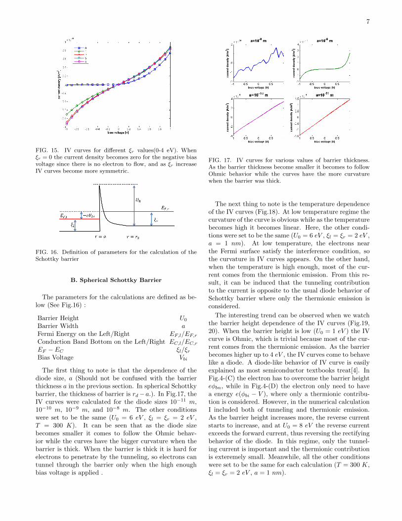
The first thing to note is that the dependence of thediode size, a (Should not be confused with the barrierthickness a in the previous section. In spherical Schottkybarrier, the thickness of barrier is rd−a.). In Fig.17, theIV curves were calculated for the diode sizes 10−11 m,10−10 m, 10−9 m, and 10−8 m. The other conditionswere set to be the same (U0 = 6 eV , ξl = ξr = 2 eV ,T = 300 K). It can be seen that as the diode sizebecomes smaller it comes to follow the Ohmic behav-ior while the curves have the bigger curvature when thebarrier is thick. When the barrier is thick it is hard forelectrons to penetrate by the tunneling, so electrons cantunnel through the barrier only when the high enoughbias voltage is applied .
FIG. 17. IV curves for various values of barrier thickness.As the barrier thickness become smaller it becomes to followOhmic behavior while the curves have the more curvaturewhen the barrier was thick.
The next thing to note is the temperature dependenceof the IV curves (Fig.18). At low temperature regime thecurvature of the curve is obvious while as the temperaturebecomes high it becomes linear. Here, the other condi-tions were set to be the same (U0 = 6 eV , ξl = ξr = 2 eV ,a = 1 nm). At low temperature, the electrons nearthe Fermi surface satisfy the interference condition, sothe curvature in IV curves appears. On the other hand,when the temperature is high enough, most of the cur-rent comes from the thermionic emission. From this re-sult, it can be induced that the tunneling contributionto the current is opposite to the usual diode behavior ofSchottky barrier where only the thermionic emission isconsidered.
The interesting trend can be observed when we watchthe barrier height dependence of the IV curves (Fig.19,20). When the barrier height is low (U0 = 1 eV ) the IVcurve is Ohmic, which is trivial because most of the cur-rent comes from the thermionic emission. As the barrierbecomes higher up to 4 eV , the IV curves come to behavelike a diode. A diode-like behavior of IV curve is easilyexplained as most semiconductor textbooks treat[4]. InFig.4-(C) the electron has to overcome the barrier heighteφbn, while in Fig.4-(D) the electron only need to havea energy e(φbi − V ), where only a thermionic contribu-tion is considered. However, in the numerical calculationI included both of tunneling and thermionic emission.As the barrier height increases more, the reverse currentstarts to increase, and at U0 = 8 eV the reverse currentexceeds the forward current, thus reversing the rectifyingbehavior of the diode. In this regime, only the tunnel-ing current is important and the thermionic contributionis exteremely small. Meanwhile, all the other conditionswere set to be the same for each calculation (T = 300 K,ξl = ξr = 2 eV , a = 1 nm).

8
FIG. 18. The temperature dependence of the IV curves.At low temperature the tunneling current dominates thethermionic current, thereby the reverse current is observed.As the temperature becomes high the diode behavior startsto appear, and in extremely high temperature it eventuallybecomes Ohmic.
FIG. 19. IV curves for the various barrier height values (smallU0 regime). At U0 = 0, it’s Ohmic since almost all of thecurrent comes from the thermionic emission. As the barrierheight becomes larger, the diode-behavior is observed, whichcan be explained in the general terms like many other semi-conductor textbooks.
Finally, another interesting behavior is shown in IVcurves for the different ξr values (Fig.21). The other con-ditions were set to be the same (T = 300 K, ξl = 2 eV ,a = 1 nm, U0 = 6 eV ). At ξr = 1 eV , rectifying behaviorof the diode is reversed. The region is the same as the dis-cussion before. When the tunneling contribution to the
FIG. 20. The IV curves for the various barrie height values(large U0 regime). As the barrier height becomes larger, thereverse current appears, thereby reversing the rectifying be-havior of the Schottky diode.
FIG. 21. IV curves for the various ξr values. At ξr = 1 eV ,IV curve is is opposite to the usual Schottky diode. In thisregime the tunneling current dominates the thermionic cur-rent. As ξr increases, the thermionic emission current startsto contribute, thereby the diode-behavior starts to appear.
current dominates the thermionic contribution, the recti-fying behavior is reversed. As the ξr value increases thethermionic current starts to contribute, thus the usualdiode behavior of the Schottky barrier is observed.

9
CONCLUSION
In this paper, the contact between the metal tip andn-type semiconductor contact is modeled as a Schottkycontact barrier. Using the depletion approximation, thePoisson equation was solved to get the shape of the poten-tial barrier. Then, by plugging in the potential barriercalculated before, the Schrodinger equation was solvedand the transmission coefficient was calculated. Finally,combined with the Fermi-Dirac function, the current den-sity was calculated.
It was observed that when thermionic current domi-nates the tunneling current contribution (high T , largea, small U0, large ξ) the IV curve just follows the usualdiode behavior, which can be explained like many othersemiconductor textbooks. However, when tunneling cur-rent dominates (low T , small a, large U0, small ξ), thereverse current starts to appear and thereby reverse therectifying behavior of the diode.
From the experimental result, it is suggested that thecurrent at the tip is composed of both tunneling andthermionic current. Since the two contributions aremixed, it would show the half-like diode IV curve.
ACKNOWLEDGEMENT
I want to acknowledge my supervisor Univ.-Prof.Ph.D. Peter Hadley for supporting me for every aspectsof this project, both theoretical and experimental. I alsowant to thank Stefan Kirnstotter for guiding me in thelaboratory and supporting the experiments.
∗ [email protected][1] http://lamp.tu-graz.ac.at/~hadley/sem/index/
index.php
[2] John G. Simmons, J. Appl. Phys. 34, 1793 (1963)[3] http://web.tiscali.it/decartes/phd\_html/node3.
html
[4] Juan Carlos Cuevas, Elke Scheer, Molecular Electronics -an introducton to theory and experiment, 2010
[4] Alexander Schnabel, Stephan Stoica, The report for theclass Electrical Measurement in a SEM
[4] B. Ven Zeghbroeck, Principles of Semiconductor Devices,Online textbook, 2011
[5] G. D. Smit, S. Rogge, T. M. Klapwijk, Appl. Phys. Lett.81, 20 (2002)
APPENDIX
Here, the matlab source code for the numerical calcu-lations is included.
A. Square Barrier
There are four function files named schrodinger, tun-neling, fermi, and current. All these files should be inthe same folder.
Function file for solving the Schrodinger equation
function dy=schrodinger(t,y)
dy=zeros(2,1);
global Ex a Vx V0 xsir
m=9.10938188*10^(-31);
hbar=(6.626068*10^(-34))/(2*pi);
e=1.60217646*10^(-19);
dy(1)=y(2);
dy(2)=y(1)*2*m
*((e*V0+xsir) - e*Vx*(1-t/a) - Ex)/(hbar^2);
Fermi function file
function [ f ] = fermi(E)
global Temp kB
f=1/( exp(E/(kB*Temp)) + 1);
end
Function file that gives the current density for the energylevel E - E+dE
function [dJ]=tunneling(V)
global e hbar E kB Temp Ex Vx V0 Vx a xsil xsir
e=1.60217646*10^(-19);
m=9.10938188*10^(-31);
h=6.626068*10^(-34);
hbar=(6.626068*10^(-34))/(2*pi);
kB=1.3806503*10^(-23);
a=1*10^(-11); %barrier depth
V0=3;% barrier hight
xsil=2*e; % filled electron in LHS
xsir=2*e; % filled electron in RHS
mul=xsir-e*V;
mur=xsir;

10
Temp=300; %device temperature
Vx=V;
VR=V;
N=100; %energy step
%ground energy
ger=0;
gel=-(xsil-xsir)-e*Vx;
if (gel<0)
E=linspace(ger,max(mul,mur)+10*kB*Temp,N);
dE=E(2)-E(1);
else
E=linspace(gel,max(mul,mur)+10*kB*Temp,N);
dE=E(2)-E(1);
end
kr=sqrt(2*m*E/(hbar)^2);
kl=sqrt(2*m*(E+xsil-xsir+e*Vx)/(hbar)^2);
Ai=zeros(N,1);
Ar=zeros(N,1);
T=zeros(N,1);
dJ=zeros(N,1);
for j=1:N
Ex=E(j);
[x psi]=ode45(’schrodinger’, [a 0]
,[exp(1i*kr(j)*a) 1i*kr(j)*exp(1i*kr(j)*a)]);
nn=size(x);
n=nn(1,1);
Ai(j)=(psi(n,1)+psi(n,2)/(1i*kl(j)))/2;
Ar(j)=(psi(n,1)-psi(n,2)/(1i*kl(j)))/2;
T(j)=1-(abs(Ar(j)/Ai(j)))^2;
T1=T(j);
dJ(j)=-(4*e/h)*T1*(fermi(Ex-mul)-fermi(Ex-mur))*dE;
end
end
Function File that gives the IV curve
function [V J]=current(Vspan,Vstep)
V=transpose(linspace(Vspan(1),Vspan(2), Vstep));
J=zeros(Vstep,1);
for j=1:1:Vstep
J(j)=nansum(tunneling(V(j)));
end
figure
plot(V,J,’-o’);
end
Schottky Barrier
There are four function files named schrodinger1, tun-neling1, fermi1, and current1. All these files should bein the same folder.
Function file for solving the Schrodinger equation
function dy=schrodinger1(t,y)
dy=zeros(2,1);
global Ex rd
m=9.10938188*10^(-31);
hbar=(6.626068*10^(-34))/(2*pi);
e=1.60217646*10^(-19);
Nd=10^(21);
ep0=8.85418782*10^(-12);
epr=1;
ep=ep0*epr;
k=(e*Nd)/(6*ep);
dy(1)=y(2);
dy(2)=y(1)*2*m
*(-e*k*(3*(rd^2)-(t^2)-2*(rd^3)/t)-Ex)/(hbar^2);
Fermi function file
function [ f ] = fermi1(E)
global Temp kB
f=1/( exp(E/(kB*Temp)) + 1);
end
Function file that gives the current density for the energylevel E - E+dE
function [dJ]=tunneling1(V)
global kB Temp Ex Vx a rd
% fixed constants
e=1.60217646*10^(-19);
m=9.10938188*10^(-31);
hbar=(6.626068*10^(-34))/(2*pi);
h=6.626068*10^(-34);
kB=1.3806503*10^(-23);
ep0=8.85418782*10^(-12);
epr=1;
ep=ep0*epr;
Nd=10^(21);

11
k=(e*Nd)/(6*ep);
xsil=2*e; % chemical potential at LHS
xsir=2*e; % chemical potential at RHS
mul=xsir-e*V;
mur=xsir;
Temp=300; %device temperature
a=1*10^(-8);
Vs=-6;
Vx=V;
VR=V;
N=100; %energy step
rds=roots([2,-3*a,0,(a^3)+((Vs+Vx)*a/k)]);
rd=rds(1);
%ground energy
ger=0;
gel=-(xsil-xsir)-e*Vx;
if (gel<0)
E=linspace(ger,max(mul,mur)+10*kB*Temp,N);
dE=E(2)-E(1);
else
E=linspace(gel,max(mul,mur)+10*kB*Temp,N);
dE=E(2)-E(1);
end
kr=sqrt(2*m*E/(hbar)^2);
kl=sqrt(2*m*(E+xsil-xsir+e*Vx)/(hbar)^2);
Ai=zeros(N,1);
Ar=zeros(N,1);
T=zeros(N,1);
dJ=zeros(N,1);
for j=1:N
Ex=E(j);
[x psi]=ode15s(’schrodinger1’, [10*a a]
,[exp(1i*kr(j)*10*a) 1i*kr(j)*exp(1i*kr(j)*10*a)]);
nn=size(x);
n=nn(1,1);
Ai(j)=(psi(n,1)+psi(n,2)/(1i*kl(j)))/2;
Ar(j)=(psi(n,1)-psi(n,2)/(1i*kl(j)))/2;
T(j)=1-(abs(Ar(j)/Ai(j)))^2;
T1=T(j);
dJ(j)=-(4*e/h)*T1*(fermi1(Ex-mul)-fermi1(Ex-mur))*dE;
end
end
Function File that gives the IV curve
function [V J]=current1(Vspan,Vstep)
V=transpose(linspace(Vspan(1),Vspan(2), Vstep));
J=zeros(Vstep,1);
for j=1:1:Vstep
J(j)=nansum(tunneling1(V(j)));
end
end