modeling, stability analysis and control of a direct ac/ac matrix
TRANSCRIPT

AN ABSTRACT OF A THESIS
MODELING, STABILITY ANALYSIS AND CONTROL OF A
DIRECT AC/AC MATRIX CONVERTER BASED SYSTEMS
Melaku Mihret
Master of Science in Electrical and Computer Engineering
The AC-AC matrix converters are pulse-width modulated using either a carrier-
based pulse width modulation (PWM) or space vector modulation techniques. Both
modulation techniques are analyzed for a three phase-to-three phase matrix converter. It
is desirable to be able to synthesize the three-phase voltages with minimum harmonics
and the highest voltage gain possible.
A new methodology for designing an input filter for the matrix converter is
proposed. This approach is based on the Fourier series of the switching signals and
harmonic balance technique. The parameters of the filter are determined based on a
specified maximum allowable source current and input capacitor voltage ripple as well as
the overall system stability.
A complete dynamic modeling and a new approach of steady state analysis for an
AC/AC matrix converter fed induction motor drive are set forth. The dynamic responses
as well as the steady state performance characteristics of the system are studied under
various load conditions while the voltage source operates under a unity power factor.
Similar modeling is also done for a matrix converter feeding a passive RL load.
A new generalized model for stability analysis based on small signal modeling is
proposed for a matrix converter fed induction motor drive system under a constant
Volt/Hertz operation. Different factors which affect the matrix converter stability are
analyzed.
A high performance vector control for a matrix converter fed induction motor
with input power factor control is set forth in this work. Detailed controller designs are
presented after studying the internal and zero dynamics of the overall drive system. The
robustness of the proposed control scheme is verified through computer simulation.
Finally, the actual firing pulses for the bidirectional switches of the matrix
converter are generated using LabVIEW/FPGA on a national instrument NIcRIO chassis.
A computer simulation has been done based on these actual pulses obtained from the
FPGA terminals.

MODELING, STABILITY ANALYSIS AND CONTROL OF A
DIRECT AC/AC MATRIX CONVERTER BASED SYSTEMS
A Thesis
Presented to
The Faculty of the Graduate School
Tennessee Technological University
By
Melaku Mihret
In Partial Fulfillment
Of the Requirements of the Degree
MASTER OF SCIENCE
Electrical Engineering
December 2011

ii
CERTIFICATE OF APPROVAL OF THESIS
MODELING, STABILITY ANALYSIS AND CONTROL OF A
DIRECT AC/AC MATRIX CONVERTER BASED SYSTEMS
By
Melaku Mihret
Graduate Advisory Committee:
Joseph Ojo, Chairperson Date
Ghadir Radman Date
Ahmed Kamal Date
Approved for the Faculty:
Francis Otuonye
Associate Vice President
for Research and Graduate Studies
Date

iii
DEDICATION
This work is dedicated to my parents

iv
ACKNOWLEDGEMENTS
I would like my deepest gratitude to the chair person of my advisory committee,
Dr. Joseph Ojo for his expertise guidance, generous support and encouragement during
the course of the research. I would also like to express my sincere thanks to Dr. Ghadir
Radman and Dr. Ahmed Kamal for their effort in reviewing and evaluating my work.
I am grateful to the office of Center for Energy Systems Research (CESR) for the
financial support provided during my graduate study. I would also like to thank ECE
department for creating nice atmosphere and kind treatment with special thanks goes to
Mr. Robert Peterson and Mr Conard Murray for their invaluable support.
I owe my deepest gratitude to Meharegzi Abrham for his time in all the technical
discussions throughout my thesis. And I would also thank him and his wife Elizabeth for
their care and support. I would like to thank Sosthenes, Hossein, Kennedy, Jeff, Mehari
and Will. I am so grateful to my roommates Bijaya, Amrit and Puran for their technical
support and making my stay so cherished.
It is my great pleasure to thank my friends Abebe, Ahmed, Wende and Abel for
their friendship and moral support. I extend my sincere thanks to Dr. Solomon Bekele for
his advice.
My heartfelt appreciation goes toward my families for their unconditional love
and encouragement in all my endeavors.
Lastly, I offer my regards and blessings to all of those who supported me in any
respect during the completion of the work.

v
TABLE OF CONTENTS
Page
LIST OF TABLES………….…………………...…………………………………...….xi
LIST OF FIGURES.……..…………………………………………..……………….…xii
CHAPTER 1 ........................................................................................................................1
INTRODUCTION ...............................................................................................................1
1.1 Introduction ...........................................................................................................1
1.2 Overview of Static AC/AC Power Frequency Conversion ...................................1
1.2.1 Indirect Power Frequency Converter ............................................................ 2
1.2.2 Direct AC/AC Converter .............................................................................. 4
1.3 Objectives of the Thesis ........................................................................................6
1.4 Thesis Outline .......................................................................................................7
CHAPTER 2 ......................................................................................................................10
LITERATURE REVIEW ..................................................................................................10
2.1 Modulation Strategies .........................................................................................10
2.2 Input Filter Design ..............................................................................................12
2.3 Stability Analysis of a Matrix Converter System ...............................................14
2.4 Control of Matrix Converter Drive System ........................................................15
CHAPTER 3 ......................................................................................................................19

vi
Page
MODULATION TECHNIQUES ......................................................................................19
3.1 Introduction .........................................................................................................19
3.2 Carrier Based Modulation ...................................................................................19
3.2.1 Switching Signal Generations ..................................................................... 24
3.3 Space Vector Modulation ....................................................................................26
3.3.1 Direct Space Vector modulation ................................................................. 26
3.3.2 Indirect Space Vector modulation .............................................................. 45
3.3.3 Common Mode Voltage Expression Based on Duty Cycle Space Vector
Modulation ................................................................................................................ 60
3.4 Simulation Results and Discussion .....................................................................75
3.5 Conclusion ..........................................................................................................83
CHAPTER 4 ......................................................................................................................85
INPUT FILTER DESIGN .................................................................................................85
4.1 Introduction .........................................................................................................85
4.2 Fourier Series Analysis of Switching Signals of a Matrix Converter .................86
4.3 Input Filter Parameters Specification ..................................................................97
4.3.1 Harmonic Balance Technique ..................................................................... 99
4.3.2 Stability Analysis for Matrix converter feeding an RL load..................... 106

vii
Page
4.4 Simulation Results and Discussion ...................................................................111
4.5 Conclusion ........................................................................................................118
CHAPTER 5 ....................................................................................................................119
DYANMIC AND STEADY STATE MODELLING OF MATRIX CONVERTER
SYSTEMS .......................................................................................................................119
5.1 Introduction .......................................................................................................119
5.2 Matrix Converter Feeding an RL Load .............................................................120
5.2.1 Dynamic Modelling .................................................................................. 120
5.2.2 Dynamic Simulation Results and Discussion ........................................... 127
5.2.3 Generalized Steady State Analysis ........................................................... 131
5.2.4 Steady State Simulation Results and Discussions .................................... 136
5.3 Modelling of Matrix Converter Fed Induction Machine ..................................139
5.3.1 Dynamic Modelling .................................................................................. 139
5.3.2 Dynamic Simulation Results and Discussion ........................................... 141
5.3.3 Generalized Steady State Analysis ........................................................... 144
5.3.4 Steady State Simulation Results and Discussions .................................... 147
5.4 Conclusion ........................................................................................................150
CHAPTER 6 ....................................................................................................................151

viii
Page
6.1 Introduction .......................................................................................................151
6.2 Modeling of the Drive System ..........................................................................152
6.3 Small Signal Analysis .......................................................................................157
6.4 Simulation Results and Discussions .................................................................162
6.5 Steady State Operating Conditions ...................................................................168
6.6 Simulation Result for Volt/Hz Control .............................................................170
6.7 Conclusion ........................................................................................................174
CHAPTER 7 ....................................................................................................................175
VECTOR CONTROL OF MATRIX CONVERTER FED INDUCTION MACHINE ..175
7.1 Introduction .......................................................................................................175
7.2 Field Oriented Control for Matrix Converter Fed Induction Motor with Unity
Input Power Factor Control .........................................................................................176
7.2.1 Indirect Field Oriented Control ................................................................. 176
7.2.2 Unity Input Power Factor Control ............................................................ 181
7.2.3 Input-Output Feedback Linearization ....................................................... 183
7.2.4 Stator Flux Estimation .............................................................................. 202
7.3 Simulation Results and Discussions .................................................................208
7.4 Conclusion ........................................................................................................222

ix
Page
CHAPTER 8 ....................................................................................................................223
SWITCHING SIGNALS GENERATION IN NI-cRIO CHASIS ...................................223
8.1 Introduction .......................................................................................................223
8.2 Switching signal generation using direct digital synthesis ...............................224
8.2.1 Accumulator .............................................................................................. 225
8.2.2 Lookup Table ............................................................................................ 226
8.3 Conclusion ........................................................................................................232
CHAPTER 9 ....................................................................................................................233
CONCLUSSION AND FUTURE SUGGESTION .........................................................233
9.1 Summary of the Thesis .....................................................................................233
9.2 List of Contributions .........................................................................................236
9.3 Future Work ......................................................................................................237
REFERENCES ................................................................................................................241
APPENDIX A ..................................................................................................................253
APPENDIX B ..................................................................................................................270
APPENDIX C ..................................................................................................................293
APPENDIX D ..................................................................................................................298
APPENDIX E ..................................................................................................................305

x
Page
APPENDIX F ..................................................................................................................319
VITA ................................................................................................................................330
xi
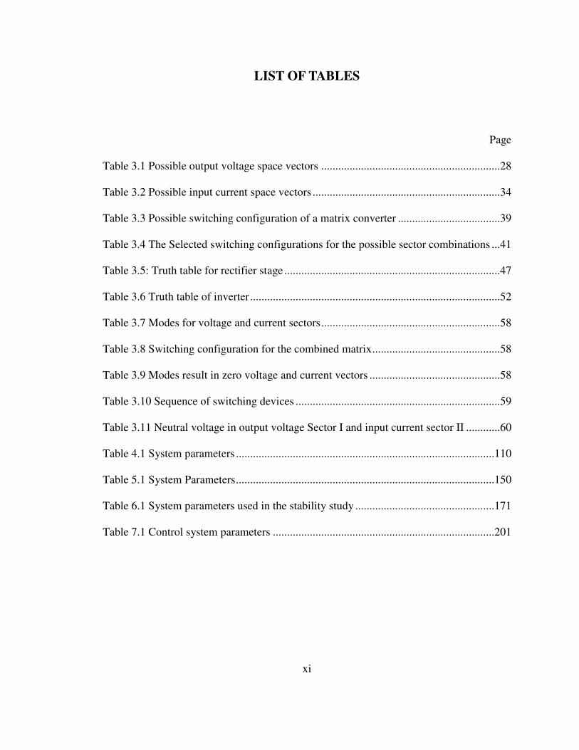
LIST OF TABLES
Page
Table 3.1 Possible output voltage space vectors ...............................................................28
Table 3.2 Possible input current space vectors ..................................................................34
Table 3.3 Possible switching configuration of a matrix converter ....................................39
Table 3.4 The Selected switching configurations for the possible sector combinations ...41
Table 3.5: Truth table for rectifier stage ............................................................................47
Table 3.6 Truth table of inverter ........................................................................................52
Table 3.7 Modes for voltage and current sectors ...............................................................58
Table 3.8 Switching configuration for the combined matrix .............................................58
Table 3.9 Modes result in zero voltage and current vectors ..............................................58
Table 3.10 Sequence of switching devices ........................................................................59
Table 3.11 Neutral voltage in output voltage Sector I and input current sector II ............60
Table 4.1 System parameters ...........................................................................................110
Table 5.1 System Parameters ...........................................................................................150
Table 6.1 System parameters used in the stability study .................................................171
Table 7.1 Control system parameters ..............................................................................201

xii
LIST OF FIGURES
Page
Figure 1.1 Diode rectifier-PWM VSI converter ..................................................................3
Figure 1.2 PWM rectifier-PWM VSI converter ..................................................................3
Figure 1.3 Direct three phase-to-three phase matrix converter ...........................................5
Figure 3.1 A schematics of a simplified matrix converter .................................................21
Figure 3.2: Illustration of voltage ratio of a) 50%, (b) 75% and (c) 86.7% ......................24
Figure 3.3 Generation of switching pulses for phase ‘a’ ...................................................25
Figure 3.4 Output voltage space vectors ............................................................................40
Figure 3.5 Input current space vector ................................................................................40
Figure 3.6 Output voltage vector synthesis .......................................................................41
Figure 3.7 Input current vector synthesis ..........................................................................43
Figure 3.8 Equivalent circuit for indirect matrix converter ...............................................46
Figure 3.10 Rectifier current space vector .........................................................................48
Figure 3.9 Diagram for synthesis of the reference current ................................................50
Figure 3.11 Inverter voltage space vector ..........................................................................53
Figure 3.12 Diagram for synthesis of the reference voltage ..............................................53
Figure 3.13 Modulation signals for output phase ‘a’ voltage ............................................77
Figure 3.14 FFT for the modulation signal MaA ................................................................77
Figure 3.15 Carrier based pulse width modulation ............................................................78
Figure 3.16 Intermediate signals used to generate switching signals ................................78

xiii
Page
Figure 3.17 Switching signals for output phase ‘a’ voltage ..............................................79
Figure 3.18 Modulation signals for output phase ‘b’ voltage ............................................79
Figure 3.19 Switching signals for output phase ‘b’ voltage ..............................................80
Figure 3.20 Modulation signals for output phase ‘c’ voltage ............................................80
Figure 3.21 Switching signals for output phase ‘c’ voltage ..............................................81
Figure 3.22 Input three phase voltages ..............................................................................81
Figure 3.23 synthesized output three phase voltages .........................................................82
Figure 3.24 Phase ‘a’ input capacitor voltage and input matrix converter current with
unity input power factor…………………………………………………………………83
Figure 4.1 Schematics of input filter circuit ......................................................................98
Figure 4.2 A matrix converter feeding an RL load ..........................................................100
Figure 4.3 Dominant harmonics components of the input current ..................................101
Figure 4.4 Stability limit of a matrix converter with RL load .........................................112
Figure 4.5 Dominant Eigen Values for various damping resistance ...............................112
Figure 4.6 Phase ‘a’ source voltage and current ..............................................................113
Figure 4.7 Phase ‘a’ input capacitor voltage and current of the MC ...............................113
Figure 4.8 Phase ‘a’ output voltage and current ..............................................................114
Figure 4.9 Input current and source current .....................................................................114
Figure 4.10 FFT of input current of the MC ....................................................................115
Figure 4.11 FFT of the source current .............................................................................115
Figure 4.12 FFT of the input capacitor voltage ...............................................................116
Figure 4.13 Stability limit for a load current of 5A .........................................................117

xiv
Page
Figure 4.14 Bode plot of the designed input filter ...........................................................117
Figure 5.1 Schematic diagram of AC/AC matrix converter feeding an RL load ............121
Figure 5.2 Switching pulses for phase ‘a’ output voltage ...............................................127
Figure 5.4 MC output three phase voltages .....................................................................128
Figure 5.5 Input three phase capacitor voltages ..............................................................129
Figure 5.6 Filtered three phase capacitor voltages ..........................................................129
Figure 5.7 MC three phase input current .........................................................................130
Figure 5.8 Three phase source currents ...........................................................................130
Figure 5.9 Output active and reactive power for possible output power factor operations
......................................................................................................................................... 136
Figure 5.10 Input active and reactive powers ..................................................................137
Figure 5.11 Magnitude of input capacitor voltage ...........................................................137
Figure 5.12 Magnitude of source current.........................................................................138
Figure 5.13 Converter output to input voltage ratio ........................................................138
Figure 5.14 Schematic diagram of the AC/AC matrix converter fed induction motor ...140
Figure 5.15 Starting transient and dynamic response of (a) rotor speed and (b)
electromagnetic torque .................................................................................................... 142
Figure 5.16 MC output (a) line-to-line voltage (b) phase voltage ...................................142
Figure 5.17 (a) Input capacitor phase voltage (b) filtered capacitor voltage ...................143
Figure 5.18 (a) MC input phase current (b) source phase current ...................................143
Figure 5.19 Steady state torque-slip characterstics of an induction machine ..................148
Figure 5.20 Magnitude of capacitor voltage and (b) magnitude of source current .........148

xv
Page
Figure 5.21 (a) Active power and (b) reactive power drawn from the source .................149
Figure 6.1 Schematic diagram of the AC/AC matrix converter fed induction motor .....153
Figure 6.2 Stability limit of matrix converter gain against filter time constant ..............164
Figure 6.3 Matrix converter stability limit for varying Filter time constant....................164
Figure 6.4 Stability limit of the matrix converter for varying damping resistance .........165
Figure 6.5 The impact of Stator and rotor resistance on the stability of the system .......165
Figure 6.6 The impact of power factor on the stability of the system .............................166
Figure 6.7 (a) Rotor speed and (b) electromagnetic torque .............................................167
Figure 6.8 Output line to line voltage and (b) input capacitor phase voltage ..................167
Figure 6.9 MC input phase current and (b) source phase current ....................................168
Figure 6.10 Induction motor Electromagnetic torque ......................................................172
Figure 6.11 Magnitude of source current.........................................................................172
Figure 6.12 Converter voltage transfer ratio against rotor speed. ...................................173
Figure 6.13 Ratio of reactive power to the apparent power at the input of the converter
......................................................................................................................................... 173
Figure 7.1 Schematic diagram of the matrix converter fed induction motor without
damping resistor .............................................................................................................. 177
Figure 7.2 Control input and output of the system ..........................................................185
Figure 7.3 Linearization diagram for rotor flux controllers.............................................192
Figure 7.4 Block diagram for the rotor speed controller .................................................193
Figure 7.5 Inner stator current controller block diagram .................................................196
Figure 7.6 Block diagram for the input current controllers .............................................198

xvi
Page
Figure 7.7 Block diagram for the input current controllers .............................................200
Figure 7.8 Bock diagram of the stator flux estimation using LPF ...................................204
Figure 7.9 Block diagram of the proposed control scheme .............................................207
Figure 7.10 Simulink model of the proposed control scheme .........................................209
Figure 7.11 Speed command, actual speed and electromagnetic torque .........................210
Figure 7.12 Estimated and reference rotor flux linkages .................................................211
Figure 7.13 Actual and reference stator currents .............................................................211
Figure 7.14 Source currents commands and actual values ..............................................212
Figure 7.15 Inner capacitor voltage controller’s reference and actual values .................212
Figure 7.16 Matrix converter output and input capacitor voltage ...................................213
Figure 7.17 Phase ‘a’ source current and reactive power drawn from the source ...........213
Figure 7.18 Speed command, actual speed and electromagnetic torque .........................214
Figure 7.19 Estimated and reference rotor flux linkages .................................................215
Figure 7.20 Source currents commands and actual values ..............................................216
Figure 7.21 Actual and reference stator currents .............................................................216
Figure 7.22 Inner capacitor voltage controller’s reference and actual values .................217
Figure 7.23 Phase ‘a’ source current and reactive power drawn from the source ...........217
Figure 7.24 Speed command, actual speed and electromagnetic torque .........................218
Figure 7.25 Estimated and actual rotor flux linkages ......................................................219
Figure 7.26 Source currents commands and measured values ........................................219
Figure 7.27 Actual and reference stator currents .............................................................220
Figure 7.28 Inner capacitor voltage controller’s reference and actual values .................220

xvii
Page
Figure 7.29 Matrix converter output and input capacitor voltage ...................................221
Figure 7.30 Phase ‘a’ source current and reactive power drawn from the source ...........221
Figure 8.1 Controller used to generate the switching signals ..........................................224
Figure 8.2 FPGA direct digital syntheses ........................................................................227
Figure 8.3 Ch1-SaA, Ch2-SbA and Ch3-ScA .................................................................228
Figure 8.4 Switching signals for phase ‘a’ output voltage ..............................................229
Figure 8.5 Switching signals for phase ‘b’ output voltage ..............................................229
Figure 8.6 Switching signals for phase ‘c’ output voltage ..............................................230
Figure 8.7 Three phase voltages at the input terminal of MC .........................................231
Figure 8.8: Three phase output voltage of MC ................................................................231
Figure 9.1 Block diagram for the experimental set up ....................................................238
Figure 9.2 Laboratory prototype 3x3 matrix converter ...................................................239
Figure 9.3 Current sensor-FPGA interface board ............................................................239
Figure 9.4 Compact cRio-FPGA interfacing board .........................................................240
Figure F.1 (a) Single phase inverter leg, (b) carrier signal ..............................................327
Figure F.2 Theoretical results based on derived expressions ..........................................327
Figure F.3 FFT results-a simulation time of 1/400 times the switching frequency. ........328
Figure F.4 Symmetrical regular sampling. ......................................................................328
Figure F.5 Asymmetrical regular sampling. ....................................................................329
Figure F.6 FFT results for natural sampling ....................................................................330
Figure F.7 FFT results for symmetrical regular sampling ...............................................330
Figure F.8 FFT results for asymmetrical regular sampling .............................................331
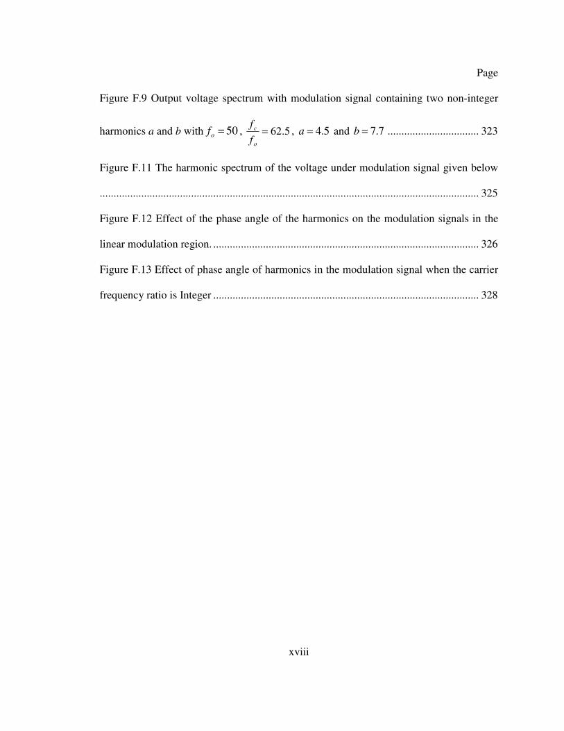
xviii
Page
Figure F.9 Output voltage spectrum with modulation signal containing two non-integer
harmonics a and b with 50=of , 5.62=o
c
f
f, 5.4=a and 7.7=b ................................. 323
Figure F.11 The harmonic spectrum of the voltage under modulation signal given below
......................................................................................................................................... 325
Figure F.12 Effect of the phase angle of the harmonics on the modulation signals in the
linear modulation region. ................................................................................................ 326
Figure F.13 Effect of phase angle of harmonics in the modulation signal when the carrier
frequency ratio is Integer ................................................................................................ 328

1
CHAPTER 1
INTRODUCTION
1.1 Introduction
This chapter gives a brief overview on the static AC/AC power frequency
conversion structures and introduces the matrix converter (MC), which is the topic of this
thesis. This thesis focuses on the modulation schemes, input filter design, modelling and
stability analysis of a direct AC/AC three phase to three phase matrix converter feeding a
passive load as well as an induction motor. It also presents vector control of a matrix
converter fed induction motor. The objectives of this work are clearly described. And
finally, the organization of the thesis is presented.
1.2 Overview of Static AC/AC Power Frequency Conversion
The first study of direct AC/AC frequency converters was presented in 1976 by
Gyugyi and Pelly [1]. In a general sense, an AC/AC power frequency conversion is the
processes of transforming AC power of one frequency to AC power of another frequency.
In addition to the capability of providing continuous control of the output frequency
relative to the input frequency the power frequency converter provide a continuous
control of the amplitude of the output voltage. These converters have inherent
bidirectional power flow capability.

2
The major application of this converter is in variable-speed AC motor drive. Here
the converter generates output voltage with continuously variable frequency and
amplitude from a fixed frequency and amplitude input AC voltage source for the purpose
of controlling the speed of an AC machine. The second application is providing a closely
regulated fixed-frequency output from input source of varying frequency. The third major
application is as reactive power compensator for an AC system. Here the power
frequency converter is used essentially as a continuously variable reactance providing
controllable reactive power for the AC system.
Static power frequency converters can be divided in to two main categories. The
first type is a two stage power converter with an intermediate DC link called indirect
AC/DC/AC power frequency converter. The second type is called a direct AC/AC power
frequency converter. This latter type is a one stage power converter which consists
basically of an array of semiconductor switches connected directly between the input and
output terminals.
1.2.1 Indirect Power Frequency Converter
The most traditional topology for AC/AC power converter is a diode rectifier
based pulse width modulated voltage source inverter (PWM-VSI) which is shown in
Figure 1.1. This consists of two power stages and an intermediate energy storage element.
In the first stage the AC power is converted to uncontrolled DC power by the means of a
diode rectifier circuit. The converted DC power is then stored in DC link capacitor.

3
Figure 1.1 Diode rectifier-PWM VSI converter
Figure 1.2 PWM rectifier-PWM VSI converter

4
In the second stage a high frequency switching operated PWM-VSI generates AC signals
with arbitrary amplitude and frequency.
Although this type of AC/AC converter is very cost-effective and reliable, it has
lots of drawbacks. Due to the uncontrolled operations of diode rectifiers, the current
drawn by the rectifier contains a large amount of unwanted harmonics with poor power
factor. The other topology for AC/AC power converter replaces the diode bridge with
PWM rectifier resulting in a back-to-back converter as shown in Figure 1.2. This
converter overcomes the input harmonic problem of the former topology.
1.2.2 Direct AC/AC Converter
The direct AC/AC converter provides a direct connection between the input and
output terminals without an intermediate energy storage element through an array of
semiconductor switches. A direct converter can be identified as three distinct topological
approaches. The first and simplest topology can be used to change the amplitude of an
AC waveform. It is known as an ac controller and functions by simply chopping
symmetric notches out of the input waveform. The second can be utilized if the output
frequency is much lower than the input source frequency. This topology is called a cyclo-
converter, and it approximates the desired output waveform by synthesizing it from
pieces of the input waveform. The last is the matrix converter and it is most versatile
without any limits on the output frequency and amplitude. It replaces the multiple
conversion stages and the intermediate energy storage element by a single power
conversion stage, and uses a matrix of semiconductor bidirectional switches,

5
Figure 1.3 Direct three phase-to-three phase matrix converter
There are many advantages presented by the matrix converter compared to the
indirect power frequency converters. The main features of matrix converter are the
following [1-20].
• Unlike naturally commutated cyclo-converters, the output frequency of a
MC can be controlled in wide ranges which can be higher or lower than
the input frequency.
• MC does not have the large energy storage element which results in a
compact power circuit. This makes MC attractive for applications
demanding compact size.
• For the matrix converter, input power factor can be controlled for any
output load. Hence, unity power factor control can be easily realized
• It has inherent bidirectional power flow capability

6
• MC has a sinusoidal input current and output voltage.
• It has found utility in high temperature, high vibration and low
volume/weight applications such as aerospace
However, it has the following disadvantages
• Although the absence of the DC link capacitor makes the converter compact, it
decreases the maximum amplitude of the output voltage to be 86.67% of the input
voltage amplitude.
• Relatively large number of semiconductor switches and driver circuits are
required compared to AC/DC/AC converter. The MC requires 18 IGBTs
(Insulated Gate Bipolar Transistor) and 18 fast recovery diodes where as the
indirect converter only require 12 IGBTs and 12 fast recovery diodes. Therefore,
this increases the cost of the converter and affects the overall system reliability.
1.3 Objectives of the Thesis
The major objectives of the thesis are as follows
• To adapt space vector modulation, both direct and indirect space vector
modulations, and carrier based pulse width modulation techniques on a three
phase-to-three phase matrix converter.
• To design an input filter based on the Fourier series analysis of the switching
signals.

7
• To examine the transient and steady state response of a matrix converter feeding a
passive load as well as induction motor along with the interaction between the
interaction between the input and outputs through this converter.
• To derive a generalized steady state performance analysis which can be used for
unity as well as non-unity input power factor operations.
• To examine the different factors which affect the stability of a matrix converter
fed induction motor drives.
• To develop a control scheme which consists of vector control for a MC fed
induction motor and input unity power factor regulation.
1.4 Thesis Outline
This thesis is categorized in nine chapters. Chapter 1 presents the overview of an
AC/AC power frequency converter. The different topologies of indirect AC/AC
converters along with the operational principles and features are introduced. The
drawbacks and limitations of these topologies are also included. The matrix converter
topology and operations are presented. Detailed comparisons between the indirect and
direct AC/AC converters are also included. This chapter also gives clear research
objectives of the thesis followed by the organization of the thesis. Then, reviews of
previous work for the matrix converter are addressed in chapter 2.

8
In chapter 3, both space vector and carrier based pulse width modulation
techniques for the most known three phase-to-three phase matrix converter are derived
and presented in detail. The space vector modulation techniques are analyzed into two
categories, direct and indirect space vector approaches. The generation of the actual
switching pulses from the modulation signals are demonstrated.
Design of an input filter for a matrix converter system are presented in chapter 4
along with complete step by step derivation for Fourier representation of switching
signals of the MC. The methods used in this thesis are based on the maximum allowable
source current and input capacitor voltage ripple as well as the stability of the overall
system.
Chapter 5 presents the complete dynamic modelling of MC fed induction motor
and a MC connected to a linear RL load. Simulations are done in both cases to examine
the transient and steady state response of the overall system. Generalized steady state
formulations are also presented considering both cases which helps to analyze the system
operating in both unity and non-unity input power factor operations. This chapter also
includes the computer simulation results of dynamic and steady state performance
characteristics and it also provides comparisons between these two results.
In chapter 6, a new generalized model for stability analysis for a MC fed
induction motor based on small signal modeling is proposed. This approach considers the
analysis when the drive system operates at unity as well as non-unity input power factor
at the source side. With the help of this model, different factors which affect the matrix
converter stability are analyzed including stator and rotor resistance variation due to
motor heating and the impact of non-zero reactive power at the source side. Computer

9
simulations are carried out to verify theoretical analysis on stability as well as on the
steady state performance characteristics.
A high performance vector control of matrix converter fed induction motor is
presented in chapter 7. In this chapter, an indirect rotor field oriented control (FOC) is
developed along with unity power factor control in the source side. The chapter also
includes a thorough controller designs and non-linear feedback linearization techniques
as the overall system is nonlinear. A proposed control scheme is verified using computer
simulation. Results are also included which verify the controllers’ robustness.
Chapter 8 gives a brief overview on the progress in the experimental results is
presented. The actual nine switching signals are generated with an NI instruments
compact RIO in a LabVIEW FPGA environment. The validity of these signals is proved
using a computer simulation.
Finally, the concluding remarks and summary of the work is presented in chapter
9. Moreover, the contributions of this research work and future suggestions are included
in this chapter.
10
CHAPTER 2
LITERATURE REVIEW
A survey of literature reviews related to this thesis is presented in this chapter. The
chapter consists of four sections. In the section 2.1, the different modulation strategies for
matrix converter are reviewed. Section 2.2 discusses a survey of input filter design
techniques developed for this converter. The works done related to the stability of a
matrix converter system are presented in section 2.3. Finally in section 2.4, existing
control methods for the matrix converter are described.
2.1 Modulation Strategies
It is very important to study the modulation strategies of a matrix converter because
the actual firing pulses of the nine bidirectional switches are generated through these
appropriate modulation signals [75,81]. Modulation methods of matrix converter are
complex and are generally classified in two different groups, the carrier-based (duty-
cycle) modulation and the space-vector modulation (SVM). A first solution has been
proposed in [2] obtained by using the duty-cycle approach. This strategy allows the
control of the output voltages magnitude and frequency and input power factor. The
maximum voltage transfer ratio of this modulation scheme is limited to 0.5. A solution
which improves maximum voltage transfer ratio to 0.866 has been presented in [3] by
including a third harmonics of the input and output voltage waveforms into the

11
modulation signals. As demonstrated in [4], the inclusion of only input third harmonics
improves the maximum ratio to 0.75 and further inclusion of output third harmonic lead
to the maximum possible voltage ratio. It is necessary to note that this value is a
theoretical maximum voltage transfer ratio of a three phase-to-three phase matrix
converter under balanced input and output voltages under unity power factor at the input
of the matrix converter. This output voltage-to-input voltage transfer ratio is greatly
decreased when the converter operates at non-unity power factor. However, the
improvement in the range of operation of a matrix converter under non-unity power
factor is presented in [67]. These duty cycle approaches in matrix converter are further
investigated for voltage source and current source converters [5].
The second type of modulation technique is Space Vector Modulation (SVM)
which can be further categorized into direct and indirect SVM. The indirect SVM
approach, which is first implemented in [6], introduces an imaginary dc link which
fictitiously divides the matrix converter into a rectifier and an inverter stages. A
generalized PWM technique based on indirect SVM is implemented in [27] which
permits independent control of the input current and output voltage and the detailed
techniques of implementation is presented in [28]. However, the direct SVM compresses
the modulation process since it does not need imaginary dc link. Besides, direct SVM
gives the maximum possible voltage transfer ratio with the addition of the third-harmonic
components which is first implemented in [7]. A general and complete solution to the
problem of the modulation strategy of three phase-to-three phase matrix converters is
presented in [26]. In [29], performance evaluations of these modulation schemes along
with a loss reduced space vector approach are presented.

12
Recently, a new modulation strategy that improves the control range of the matrix
converter is presented in [21]. This strategy can be used to improve the performance of
the matrix converter to compensate the reactive power of the input filter capacitor
whenever is needed, or just to increase the voltage margin of an electric drive.
A space vector modulation strategy for matrix converter has been modified for
abnormal input-voltage conditions, in terms of unbalance, non-sinusoid, and surge. As
presented in [83], this modified modulation strategy can eliminate the influence of the
abnormal input voltages on output side without an additional control circuit, and three-
phase sinusoidal symmetrical voltages or currents can be obtained under normal and
abnormal input-voltage conditions.
In [84], a general form of the modulation functions for matrix converters is
derived using geometric transformation approach. This paper considers a matrix
converter as generalized three-level inverters to apply the double-carrier-based dipolar
modulation technique of the three-level inverter to the matrix converter.
2.2 Input Filter Design
The input filter in matrix convert is needed to mitigate undesired harmonic
components from injecting into the AC main line [48-56]. These undesired harmonics are
generated due to the high frequency switching of the matrix converter. On the other hand,
this filter smoothen the input current and input capacitor voltage ripples to meet the
electro-magnet interference (EMI) requirements [51]. A single stage LC filter is the most

13
commonly used filter topology since it is simple, low cost and reduced size as compared
to multi-stage and integrated filter topologies. However, the multi-stage topology
provides a better harmonic attenuation at the switching frequency [54]. The input filter
has to be designed to meet the following requirements [48-52]:
• The cut-off frequency of the filter should be lower than the switching
frequency and higher than the fundamental frequency of the input AC
source.
• The input power factor should be kept maximum for a given minimum
output power.
• The lowest volume and/or weight of capacitor and chokes is used.
• The voltage drop in the inductor should be minimum.
• The filter parameters should disturb the overall system stability.
The procedure to specify the value of the filter capacitor and inductor is presented
in detail in [50-51]. The existence of the filter circuit dominantly induces capacitive
reactive power in the line resulting in lower input power factor. This effect becomes more
significant at low power operation [51]. Therefore, the maximum value of the capacitor is
first determined based on the minimum power factor requirement at a given minimum
output power operation. The value of the minimum power factor is specified to be 0.8 in
[50-51] and 0.85 in [52] at 10% rated power operation, although there is no standard
value for it. Once the capacitor value is known, the filter inductor is determined based on
the chosen characteristic frequency. In [79], the study of different switching strategies has
been compared in terms of the rms value of the line current ripple and the result can be
used for input filter design.

14
This approach gives only the maximum value of capacitor. The lower the capacitance, the
higher the input power factor. However, lower capacitance leads to higher ripple input
voltage and current. Similar to the maximum capacitance specification, it is necessary to
determine the minimum required capacitor value corresponding to the maximum ripple
voltage or current.
Recently, an integrated analytical approach towards filter design for a three phase
matrix converter is reported in [85]. This design method addresses both general filter
design aspects like attenuation, regulation and also MC-specific issues like the damping
resistors at the input filter.
2.3 Stability Analysis of a Matrix Converter System
It is reported that the input filter can be one of the elements which possibly leads
to instability operation in MC system [11]; for this reason several works related to
stability issues are addressed using small signal and large signal modeling [7-12]. In [8],
it has been shown that filtering the input capacitor voltage has an impact on the stability
of the converter. In addition, independent filtering of the angle and the magnitude of this
input voltage has significantly improved the stability as presented in [10]. The stability of
the MC is also influenced by the grid impedance, filter inductances and capacitance and
filter time constants as intensively discussed in [10].
One of the contributions of this thesis is the presentation of a new approach of
stability analysis which does not make any assumptions on the phase angle of the input
capacitor voltage and reference output voltage. In the small signal analysis presented in

15
[39-44], the phase angle of the capacitor voltage and reference output voltage are
arbitrarily chosen to be zero which masks the effect of these angles on the stability of the
system. In addition, arbitrarily choosing the phase angle of the capacitor voltage makes it
impossible to operate at unity power factor at the source side. Therefore, it is essential to
investigate the effect of this angle on the stability of the system. This thesis also presents
a generalized steady state and small signal modeling which can be used for both zero and
non-zero reactive power at the source side. As the matrix converter may be used for
reactive power compensation, with the help of this model, the impact of non-zero reactive
power on the overall system stability is also presented. Since stator and rotor resistances
may vary up to 100% and 50%, respectively because of rotor heating [74], this work also
includes the influence of these stator and rotor resistances variation on the system
stability. Although [39] reported that adding a damping resistance across the input filter
inductor increases the power limit of the stable operation, this thesis in particular clearly
shows the effect of this variation in detail.
2.4 Control of Matrix Converter Drive System
Variable ac drives have been used in the past to perform relatively undemanding
roles [77]. Vector control technique incorporating high performance processors and DSPs
have made possible the application of induction motor and synchronous motor drives for
high performance applications where traditionally only dc drives were applied. Induction
motor drives fed by MC have been developed for the last decades [47]. The matrix
converter drive can theoretically offer better advantages over the traditional voltage

16
source inverter based drives. The main advantages that are often cited are the
compactness, the bidirectional power flow capability and the higher current quality [67].
A new and relatively simple sensorless control for induction motor drives fed by
matrix converter using the imaginary power flowing to the motor and the constant air gap
flux is proposed in [47]. This scheme was independent of the parameters and employs a
non linear compensation strategy to improve the performance of the speed control in the
low speed region. In [81], an improvement on the performance of the direct torque
control for matrix converter driven interior permanent magnet synchronous machine
drive was studied in detail. This is realized through the modified hysteresis direct torque
control in [80] and the associated problems with this control are also investigated.
Induction machines are widely used in the industrial drive system due to its various
advantages over other machines as regards to price, size, robustness, etc [62-64, 77].
They are very suitable for constant speed applications; however, the controller algorithms
become more complex when used for variable speed drive [63]. Due to the great
advancement of power electronics and digital signal processing, they also offer a high
performance as well as independent control on torque and flux linkages, which is similar
to that of the DC machine. There are various control schemes available for induction
machine drives like scalar control, direct torque control, vector control and adaptive
control [77].
The scalar control is a simple and robust type of control which only considers the
magnitude variation of the machine variables and ignores the coupling effect that exists
in the machine [63]. The commonly used scalar control is Volt/Hertz control. In this
scheme the ratio of the applied voltage and frequency must be constant to maintain a

17
constant air gap flux. Generally, such control schemes are only implemented for low
performance application.
The vector control is a widely used control approach for high performance induction
machine applications [77]. Unlike scalar control, both amplitude and phase of the AC
excitation are the control variables. Vector control of the voltages and currents results in
the control of the spatial orientation of the electromagnetic fields in the machine, leads to
field orientation. Field orientation control (FOC), consists of controlling the stator current
represented by a vector. The control is based on projections which transform a three
phase time and speed dependent system into a two co-ordinate time invariant system.
This projection leads to a structure similar to that of a dc machine control. However, this
requires information about magnitude and position of rotor flux vector. A vector control
can be further categorized into a direct and indirect FOC, depending on the how the rotor
flux position is determined. If the rotor flux is directly evaluated, the control is called a
direct FOC. In indirect FOC, the stator currents are used to calculate the instantaneous
slip frequency which later be integrated and added to the measured rotor position to give
a better estimation of flux vector position. The indirect FOC can be further classified into
rotor flux, stator flux and air gap flux oriented control. In rotor flux oriented control, the
rotor flux vector is aligned in d-axis of synchronously rotating reference frame.
Therefore, the q axis rotor flux is zero.
In this thesis, the indirect rotor field oriented control for matrix converter fed
induction machine with unity input power factor control is presented to realize the high
performance control of the drive.

18
Recently, the most common control and modulation strategies are briefly reviewed in
[75]. The paper used the theoretical complexity, quality of load current, dynamic
response and sampling frequency as a measure of performance of different control
strategies. These control strategies include direct torque control (DTC), predictive current
and torque control. As reported in [75], predictive control is the best alternatives due to
its simplicity and flexibility to include additional aspects in the control. However, the
author finally concluded that it is not possible to establish which method is the best.
In [14], the model based predictive control (MPC) targeted to obtain low-distortion input
currents, controlled power factor and high performance drive even when the source
contains disturbances. Basically it applied to establishrd a method to control the current
of an induction machine. Besides it allows the control of the input current and reactive
power to the system.
Simulation plays a relevant role in the analysis and design of modern power
systems and power electronics converters. A unique method of matrix converter
simulation technique called Switching State Matrix Averaging (SSMA) in presented in
[82]. This technique drastically speeds up the simulation and provides a possibility of
simulating even more complex systems which would not be possible with in a reasonable
time frame in a conventional computer.

19
CHAPTER 3
MODULATION TECHNIQUES
3.1 Introduction
This chapter presents the two modulation strategies used for the direct matrix
converter. Complete derivation of the modulation signals for the carrier based modulation
is given in section 3.2. Both direct and indirect space vector approaches are also
presented in this chapter. The improvement in the voltage transfer ration of a matrix
converter using a third harmonic injection is illustrated. A methodology for generation of
the actual firing pulses of the bidirectional switches is demonstrated. Computer
simulation has also be done to verify the theoretical modulation technique and results
demonstrate the generation of the switching signals which synthesize the balanced set of
output three phase voltages.
3.2 Carrier Based Modulation
A typical three phase-to-three phase matrix converter consisting of nine
bidirectional switches is shown in Figure 1.1. The switching function of the bi-directional
switch connecting the input phase i to output phase j is denoted by Sij . The relevant
existence switching function Sij ( i = ap, bp, cp, and j = as, bs, cs ) defines the states of
the bi-directional switches.

20
When the switch is turned ON the switching function Sij = 1, and when turned OFF,
the switching function Sij = 0. There are two requirements must be fulfilled at any time
during switching [59, 79]. The input voltages of the MC should not be short circuited;
therefore, all three switches connected to an output phase voltage must not be turned ON
at the same time. The second requirement is that there should be always a path for the
output current; in other word, the output line must be connected all the time to a single
input line.
1
1
1
=++
=++
=++
cCbCaC
cBbBaB
cAbAaA
SSS
SSS
SSS
(3.1)
The mapping of the input phase voltages and output phase voltages of the converter are
given as:
cCcpbCbpaCappncs
cBcpbBbpaBappnbs
cAcpbAbpaAappnas
SVSVSVVV
SVSVSVVV
SVSVSVVV
++=+
++=+
++=+
(3.2)
Given the converter three phase input voltages, Vap, Vbp and Vcp the expressions for the
switching functions Sij are to be determined with the specification of the desired three
phase output voltages, Vas, Vbs and Vcs. And the Vpn is a zero sequence voltage between
the neutral point of input capacitor voltage, p, and output voltage’s neutral point, n.
Equations (3.1) and (3.2) can be written in matrix form as given below.
For two vectors X and Y related by a non-square matrix A as given in (1.4), X can be
expressed in terms of Y by inverting the fat matrix [60] by minimizing the sum of the
squares of all the elements of X.

21
Figure 3.1 A schematics of a simplified matrix converter
The inverse of the underdetermined equation can be calculated as follows.
YAX = (3.4)
YAAAXTT 1
)(−= (3.5)
43421
321
44444444 344444444 21Y
pncs
pnbs
pnas
X
cC
bC
aC
cB
bB
aB
cA
bA
aA
A
cpbpap
cpbpap
cpbpap
VV
VV
VV
S
S
S
S
S
S
S
S
S
VVV
VVV
VVV
+
+
+
=
1
1
1
111000000
000111000
000000111
000000
000000
000000
(3.3)

22
The average switching functions are determined as shown in (3.6). It is necessary to note
that Vno is the average of Vpn. This expression is general and applied for both balanced
and unbalanced input voltage.
211 )())(3)(( kVVVVkVVVVVVkS ipcpbpapcpbpapipnojsij +++−++−+= (3.6)
where the k1 and k2 are defined in (3.7)
)(2
)(2
1
222
222
2
2221
apcpcpbpbpapcpbpap
cpbpap
apcpcpbpbpapcpbpap
VVVVVVVVV
VVVk
VVVVVVVVVk
−−−++
++=
−−−++=
(3.7)
For balanced three phase input voltages and using trigonometric relations, the averaged
switching signals expressions are simplified as given in (3.8).
Therefore, the modulation signal which is the approximation of the switching signals is
determined.
+
−=
)3
2cos(
)3
2cos(
)cos(
πω
πω
ω
t
t
t
V
V
V
V
p
p
p
p
cp
bp
ap
(3.8)
where Vp and ωp is the peak of input phase voltage and input angular frequency,
respectively.
219
2
pVk = and
3
12 =k (3.9)
)(3
2
3
12 nojs
p
ip
ijij VVV
VMS ++== (3.10)

23
These expressions of modulation signal are the same as the expression given in [8]. These
give a more convenient for practical implementation. In (10), in the absence of the neutral
voltage, the output to input voltage ratio (q) is 50% which has a little drawback in real
applications. The voltage transfer ratio can be improved to 75% by adding a neutral
voltage, third harmonic of the input voltage, on the desired output voltage [4].
)3cos(4
tV
V p
p
no ω= (3.11)
This voltage ratio can further be improved to 86.7%, maximum voltage gain possible for
three phase-to-three phase matrix converter, by injecting an additional third harmonic of
the output voltage which results in an expression neutral voltage expression given in
(3.12). Vs
and ωs is the magnitude of output phase voltage and output angular frequency,
respectively.
)3cos(6
)3cos(4
tV
tV
V ss
p
p
no ωω −= (3.12)
Figure 1.2 demonstrates the effect of adding a neutral voltage improves the voltage
transfer ratio considering input balanced three phase voltage with amplitude of 1pu. The
envelope is determined using the instantaneous maximum and minimum input voltages.
If the output voltage is out of this envelope is known as over modulated. Without neutral
voltage, the output voltage cannot exceed 0.5 pu in the linear modulation region. With the
addition of a third harmonic of an input voltage, as seen in Figure 1.2b the output voltage
can be increased up to 0.75 pu and still inside the envelope. Figure 1.2c shows the
practical maximum voltage transfer limit of 0.87 using the neutral voltage expression
given in (3.12).

24
Figure 3.2: Illustration of voltage ratio of a) 50%, (b) 75% and (c) 86.7%
3.2.1 Switching Signal Generations
The actual switching pulses are generated by using the modulation signals obtained
using (3.10) with a high frequency triangular carrier signal.
-1
-0.5
0
0.5
1
(a)
-1
-0.5
0
0.5
1
(b)
-1
-0.5
0
0.5
1
(c)
Input Voltage Desired output Voltage

25
Figure 3.3 Generation of switching pulses for phase ‘a’
Generating the three switching signals for a phase ‘j’ output voltage involves two
intermediate signals. Zlj, Z2j and Z3j are the signals compared with the triangular carrier
and calculated from the modulation signals using (3.13).
13
2
1
=++=
+=
=
cjbjajj
bjajj
ajj
MMMZ
MMZ
MZ
(3.13)
After comparing the above signals with the triangular waveform, three intermediate
pulses Plj, P2j and P3j are generated. The sum of the three modulation signals which
produce an output phase ‘j’ voltage is 1 the pulse P3j is always ON.

26
1
Triag if ; 0
Triag if ; 1
Triag if ; 0
Triag if ; 1
3
2
2
2
1
1
1
=
<
>=
<
>=
j
j
j
j
j
j
j
P
Z
ZP
Z
ZP
(3.14)
Finally, the actual switching signals are determined from (3.15) where AP1 a complement
of is AP1 .
jjbj
jjbj
jaj
PPS
PPS
PS
21
21
1
=
=
=
(3.15)
Figure 1.3 shows the switching functions SaA, SbA and ScA generated using the algorithm
explained above. These pulses are used to construct output phase ‘a’ voltage and using
the similar approaches the other six switching signals are found for phase ‘b’ and phase
‘c’ output voltages.
3.3 Space Vector Modulation
3.3.1 Direct Space Vector modulation
The second type of modulation technique is called space vector modulation and it has
the following advantages over the carrier based modulation [12]:

27
• maximum voltage transfer ratio without utilizing the third harmonic component
injection method
• accommodate any input power factor independent of the output power factor
• reduce the effective switching frequency in each cycle, and thus the switching
losses
• minimize the input current and output voltage harmonics
The space vector modulation technique is based on instantaneous output voltage and
input current vectors representation. There are 27 possible switching configuration states.
However, only 21 can be usefully employed in space vector algorithm. As seen in Table
3.1, these switching states are classified into three categories:
Group I: All output terminals are connected to a particular input phases. For
example: mode AAA: all output terminals connected to input phase a voltage. These
results in a zero space vectors, hence, they are also called zero switching states.
Group II: Each output terminal is connected to a different input terminal. For
example, mode BAC- phase ‘a’ output connected to phase ‘b’ input voltage, phase ‘b’
output with phase ‘a’ input and phase ‘c’ output with phase ‘c’ input. As observed in
Table 1.1, these space vectors have constant amplitudes and rotate at the input frequency.
Therefore, these modes cannot be used to synthesize the reference vectors.
Group III: this group consists of 18 switching configurations and the two output
terminals are connected to one input terminal, and the third output terminal is connected
to one of the other input terminals. The space vectors have time varying amplitude which
depends up on the instantaneous input line-to-line voltages or output currents.

28
Table 3.1 Possible output voltage space vectors
The directions of these vectors are stationary and occupy six positions equally
spaced by 60o in qd reference frame. To determine the space vector switching strategy,
consider a balanced sinusoidal input and desired output three phase voltages.
Mode S ap S bp S cp Vas Vbs Vcs Vqs Vds Vs α s
AAA 0 0 0 V ap V ap V ap 0 0 0 -
BBB 1 1 1 V bp V bp V bp 0 0 0 -
CCC 2 2 2 V cp V cp V cp 0 0 0 -
ABC 0 1 2 V ap V bp V cp V ap -1/√3V bcp V p ω p t
ACB 0 2 1 V bp V cp V bp V ap 1/√3V bcp V p -ω p t
BAC 1 0 2 V bp V ap V cp V bp 1/√3V cap V p -ω p t+2π/3
BCA 1 2 0 V bp V cp V ap V bp -1/√3V cap V p ω p t-2π/3
CAB 2 0 1 V cp V ap V bp V cp -1/√3V abp V p -ω p t-2π/3
CBA 2 1 0 V cp V bp V ap V cp 1/√3V abp V p ω p t+2π/3
AAB 0 0 1 V ap V ap V bp 1/3V abp -1/√3V abp 2/3V abp π/3
AAC 0 0 2 V ap V ap V cp -1/3V cap 1/√3V cap 2/3V cap -2π/3
ABA 0 1 0 V ap V bp V ap 1/3V abp 1/√3V abp 2/3V abp -π/3
ABB 0 1 1 V ap V bp V bp 2/3V abp 0 2/3V abp 0
ACA 0 2 0 V bp V cp V ap -1/3V cap -1/√3V cap 2/3V cap 2π/3
ACC 0 2 2 V bp V cp V cp -2/3V cap 0 2/3V cap πBAA 1 0 0 V bp V ap V ap -2/3V abp 0 2/3V abp πBAB 1 0 1 V bp V ap V bp -1/3V abp -1/√3V abp 2/3V abp 2π/3
BBA 1 1 0 V bp V bp V ap -1/3V abp 1/√3V abp 2/3V abp -2π/3
BBC 1 1 2 V bp V bp V cp 1/3V bcp -1/√3V bcp 2/3V bcp π/3
BCB 1 2 1 V bp V cp V bp 1/3V bcp 1/√3V bcp 2/3V bcp -π/3
BCC 1 2 2 V bp V cp V cp 2/3V bcp 0 2/3V bcp 0
CAA 2 0 0 V cp V ap V ap 2/3V cap 0 2/3V cap 0
CAC 2 0 2 V cp V ap V cp 1/3V cap 1/√3V cap 2/3V cap -π/3
CBB 2 1 1 V cp V bp V bp -2/3V bcp 2/3V bcp πCBC 2 1 2 V cp V bp V cp -1/3V bcp -1/√3V bcp 2/3V bcp 2π/3
CCA 2 2 0 V cp V cp V ap 1/3V cap -1/√3V cap 2/3V cap π/3
CCB 2 2 1 V cp V cp V bp -1/3V bcp 1/√3V bcp 2/3V bcp -2π/3
Gro
up
IG
rou
p I
IG
rou
p I
II

29
+
−=
)3
2cos(
)3
2cos(
)cos(
πω
πω
ω
t
t
t
V
V
V
V
p
p
p
p
cp
bp
ap
(1.16)
+
−=
)3
2cos(
)3
2cos(
)cos(
πω
πω
ω
t
t
t
V
V
V
V
s
s
s
s
cs
bs
as
(3.17)
The output voltage space vector sV , can be resolved into two q- and d-axes. Vqs and Vds
are the q-axis and d-axis components of the output voltage space vector which can be
found using stationary qd transformation.
dsqss jVVV +=
−
−−=
cs
bs
as
ds
qs
V
V
V
V
V
2
3
2
30
2
1
2
11
2
3
The transformation used is a stationary reference frame. The two axes voltages are used
to determine the magnitude and angle of the output space vector.
)(3
1
)2(3
1
bscsds
csbsasqs
VVV
VVVV
−=
−−=
(3.18)
The magnitude and the angle, αs of the output voltage space vector are calculated for each
possible switching state using the expression (3.19).
−=
+=
−
qs
ds
s
qsqss
V
V
VVV
1
22
tanα (3.19)
30
(3.18) and (3.19) are used to determine the space vector for the output and input current
space vectors for the 27 modes.
In Table 3.1, the switching functions Sap, Sbp and Scp determine how the phase ‘a’,
‘b’ and ‘c’ output terminals are mapped with the input terminals, respectively. For
example, when the output phase a voltage is connected to input phase a voltage Sap = 0, if
it is connected to phase ‘b’, Sap = 1 and Sap = 2 when it is connected to phase c input
voltage.
Output Voltage Space Vectors. The output voltage space vectors associated to each
switching state are given in Table 3.1. These space vectors are exemplified considering
three cases, one from each group.
• Mode AAA
In this mode all the output voltage terminals are connected to input phase ‘a’ voltage.
Hence, Sap = Sbp = Scp = 0 and Vas = Vbs = Vcs = Vap. The q-axis and d-axis components of
the output voltage space vector are determined as
02
1
2
1
3
2
2
1
2
1
3
2=
−−=
−−= apapapcsbsasqs VVVVVVV
( ) ( ) 03
1
3
1=−=−= apapbscsds VVVVV
Then the magnitude and angle of the output voltage space vector becomes zero. All
modes in group I do not produce any output voltage and they are a zero switching states.
022
=+= dsqsp VVV
0tan 1 =
−= −
qs
dss
V
Vα

31
• Mode ABC
This mode belongs to group II where each output terminal is connected to different
input voltages. In this particular mode, phase ‘a’ output voltage is connected to phase ‘a’
input voltage, phase ‘b’ with phase ‘b’ and phase ‘c’ with phase ‘c’. Hence the switching
functions Sap = 0, Sbp = 1 and Scp = 2 and the output voltages Vas = Vap, Vbs = Vbp and Vcs
= Vcp. The q-axis and d-axis output voltage space vector are computed as.
apcpbpapcsbsasqs VVVVVVVV =
−−=
−−=
2
1
2
1
3
2
2
1
2
1
3
2
( ) ( ) bcpbpcpbscsds VVVVVV3
1
3
1
3
1−=−=−=
The possible input line-to-line voltage, Vab, Vbc and Vca are given as
)3
2sin(3
πω += tVV ppab
)sin(3 tVV ppbc ω=
)3
2sin(3
πω −= tVV ppca
The magnitude of all space vectors in this mode is constant and equal to the magnitude of
the input voltage. Unlike other modes, modes in this group II do not have fixed
directions. This direction rotates with the same frequency as that of the input voltage.
pbcpapdsqss VVVVVV =+=+= 2222
3
1
ttV
tV
V
Vp
pp
pp
qs
dss ω
ω
ω
α =
=
−= −−
)cos(
)sin(33
1
tantan 11

32
• Mode AAB
This mode is from the active switching groups where two of the output terminals,
phase ‘a’ and ‘b’ are both connected to phase ‘c’ input terminal. Sap = Sbp = 0 and Scp = 1
the output voltage are related with the input voltages as Vas = Vbs = Vap and Vcs = Vbp
The q-axis and d-axis output voltage space vector are determined as
abpbpapapcsbsasqs VVVVVVVV3
1
2
1
2
1
3
2
2
1
2
1
3
2=
−−=
−−=
( ) ( )abpapbpbscsds VVVVVV
3
1
3
1
3
1−=−=−=
Note that the magnitude of the space vector is time-varying with the line-to-line voltage
Vab. And the direction of this vector is fixed to 60o. All vectors in this group have fixed
direction and time varying amplitude which takes the instantaneous value of the input
line to line voltage.
abpababdsqsp VVVVVV3
2
3
1
3
122
22=
−+
=+=
( )3
3tan
3
1
3
1
tantan 111 πα ==
=
−= −−−
abp
abp
qs
dss
V
V
V
V
The complete derivation of the output voltage space vector for the 27 modes is given in
Appendix I.

33
Input current space vectors. The input current space vectors are determined based on
the output three phase currents and output power factor. Table 3.2 shows input current
space vectors for the possible 27 switching modes.
Consider a balanced three phase output current given in (3.20) with an output
power factor of ϕ s Where Is is the peak output phase current and ωs is the is the angular
frequency of the output current which is the same as the output voltage frequency.
−+
−−
−
=
)3
2cos(
)3
2cos(
)cos(
ss
ss
ss
s
cs
bs
as
t
t
t
I
I
I
I
ϕπ
ω
ϕπ
ω
ϕω
(3.20)
The magnitude and the angle, βp of the input current space vector are also computed
using the stationary qd-transformation followed by expression (3.21).
−=
+=
−
qp
dp
p
dpqpp
I
I
III
1
22
tanβ (3.21)
The calculation of input current space vector is exemplified using three modes, each
mode from different groups.

34
Table 3.2 Possible input current space vectors
Mode S ap S bp S cp I ap I bp I cp I qp I dp I p β p
AAA 0 0 0 0 0 0 0 0 0 -
BBB 1 1 1 0 0 0 0 0 0 -
CCC 2 2 2 0 0 0 0 0 0 -
ABC 0 1 2 I ap I bp I cp I ap 1/√3(I cs -I bs ) I s ω s t-φs
ACB 0 2 1 I ap I cp I bp I ap 1/√3(I cs -I bs ) I s -ω s t+φs
BAC 1 0 2 I bp I ap I cp I bp 1/√3(I cs -I as ) I s -ω s t+φs-2π/3
BCA 1 2 0 I bp I cp I ap I bp 1/√3(I cs -I as ) I s ω s t-φs+2π/3
CAB 2 0 1 I cp I ap I bp I cp 1/√3(I bs -I as ) I s -ω s t+φs-2π/3
CBA 2 1 0 I cp I bp I ap I cp -1/√3(I bs -I as ) I s ω s t-φs+2π/3
AAB 0 0 1 -I cp I cp 0 -I cp -1/√3I cs 2/√3I cs 5π/6
AAC 0 0 2 -I cp 0 I cp -I cp 1/√3I cs 2/√3I cs 7π/6
ABA 0 1 0 -I bp I bp 0 -I bp -1/√3I bs 2/√3I bs 5π/6
ABB 0 1 1 I ap -I ap 0 I ap 1/√3I as 2/√3I as -π/6
ACA 0 2 0 -I bp 0 I bp -I bp 1/√3I bs 2/√3I bs 7π/6
ACC 0 2 2 I ap 0 -I ap I ap -1/√3I as 2/√3I as π/6
BAA 1 0 0 -I ap I ap 0 -I ap -1/√3I as 2/√3I as 5π/6
BAB 1 0 1 I bp -I bp 0 I bp 1/√3I bs 2/√3I bs -π/6
BBA 1 1 0 I cp -I cp 0 I cp 1/√3I cs 2/√3I cs -π/6
BBC 1 1 2 0 -I cp I cp 0 1/√3I cs 2/√3I cs -π/2
BCB 1 2 1 0 -I bp I bp 0 1/√3I bs 2/√3I bs -π/2
BCC 1 2 2 0 I ap -I ap 0 -1/√3I as 2/√3I as π/2
CAA 2 0 0 -I ap 0 I ap -I ap 1/√3I as 2/√3I as 7π/6
CAC 2 0 2 I bp 0 -I bp I bp -1/√3I bs 2/√3I bs π/6
CBB 2 1 1 0 -I ap I ap 0 -1/√3I as 2/√3I as -π/2
CBC 2 1 2 0 I bp -I bp 0 -1/√3I bs 2/√3I bs π/2
CCA 2 2 0 I cp 0 -I cp I cp -1/√3I cs 2/√3I cs π/6
CCB 2 2 1 0 I cp -I cp 0 -1/√3I cs 2/√3I cs π/2
Gro
up
IG
rou
p I
IG
rou
p I
II

35
• Mode AAA
Since the output terminals are connected to input phase ‘a’ voltage. Hence, Sap = Sbp =
Scp = 0 and there is no path for the input currents, Iap = Ibp = Icp = 0. The q-axis and d-
axis input current space vector are determined as
( ) 03
2
2
1
2
1
3
2=++=
−−= csbsascpbpapqp IIIIIII
( ) 03
1=−= bpcpdp III
Similar to the output voltage space vectors, in this zero switching mode the magnitude
and direction of the input current space vector are both zero.
( ) 03
222=++=+= csbsasdpqpp IIIIII
0tan 1 =
−= −
qp
dp
pI
Iβ
• Mode ABC
When Sap = 0, Sbp = 1 and Scp = 2 implies Iap = Ias, Ibp = Ibs and Icp = Ics The q-axis and d-
axis input current space vector are determined as
( ) ascsbsascpbpapqp IIIIIIII =
+−=
−−=
2
1
3
2
2
1
2
1
3
2
( ) ( )bscsbpcpdp IIIII −=−=3
1
3
1
The input line-to-line currents can be defines as
)3
2sin(3
πϕω +−= sspabp tII

36
)sin(3 sspbcp tII ϕω −=
)3
2sin(3
πϕω −−= sspcap tII
The magnitude of all input current space vectors in this mode is also constant and equal
to the magnitude of the input voltage. Besides, modes in this group do not have fixed
directions. The direction of the input current rotates with the output current frequency;
therefore, they are not being used in space vector modulation.
( )2222
3
1bscsasdpqpp IIIIII −+=+=
( )
ss
as
bscs
qp
dp
p tI
II
I
Iϕωβ −=
−−
=
−= −− 3
1
tantan11
• Mode AAB
When Sap = Sbp = 0 and Scp = 1 implies Iap = -Ics, Ibp = Ics and Icp = 0 The q-axis and d-
axis input current space vector are determined as below.
cscscscpbpapqp IIIIIII −=
−−=
−−=
2
1
3
2
2
1
2
1
3
2
( )csbpcpdp IIII
3
1
3
1−=−=
The magnitude of the input current space vectors in this mode has time-varying
amplitude depending on the instantaneous output phase ‘c’ current. And the direction of
this vector is also fixed 150o. All vectors in this group have fixed direction and time-
varying amplitude which takes the instantaneous output currents.

37
cscscsdpqpp IIIIII3
2
3
1 2222=+=+=
6
53
1
tantan11 π
β =
−=
−= −−
cs
cs
qp
dp
pI
I
I
I
The complete derivation of the input current space vector for the possible 27 modes is
given in Appendix II.
Based on Table 3.1 and Table 3.2, the actual space vectors implemented in the
direct space vector modulation techniques are only 21. In other words, only group I and II
are used in the modulation. It can be also seen that the 18 non-zero space vector are
displaced with equal 60o with each other. Three of these vectors lie on the same direction
but they have different magnitudes. For example modes ACA, BAB and BAB produce an
output voltage vectors which all lie at 120o in space and similarly, CCB, BCC and CBC
comprise an input current space vector lying on 90o in space. Moreover, there are always
two space vectors having same magnitude with opposite directions. For example, Modes
AAB and BBA produces pairs of voltage space vector with equal magnitude and placed
on -120o and 60
o, respectively. And they also result in a pair of input current space
vectors of equal magnitude placed on 150o and -30
o, respectively. As a result these modes
are denoted as -7 and +7 switching states, respectively.

38
The output voltage vector and input current space vectors generated by the active
switching modes, group II, and are shown in Figure 3.4 and 3.5. Switching states +1, +2
and +3 have a direction of zero and -1, -2 and -3 switching states lie on 180o as seen in
Figure 3.4. Similarly, Figure 3.5 -60o, 90
o and -120
o corresponds to the positive switching
states and negative switching states lie on the opposite direction.
The algorithm for space vector modulation basically involves two procedures: the
selections of appropriate switching states and determine the duty cycle of the selected
switching states. To construct desired output voltage and input current simultaneously,
the states are chosen such that they are adjacent to the both output voltage and input
current vectors and they involve the lowest switching transition as possible.
Consider both the desired output voltage and input current lie on sector 1, the
vector Vs can be synthesized using two adjust vectors Vs’ and Vs
’’ as seen in Figure 3.6
corresponds to the upper and the lower adjacent vectors, respectively. Vs’
can be
synthesized using six possible switching configurations (±7, ±8, ±9) and only four of
them (±7, ±9) simultaneously allow the modulation of input current direction. Similarly,
there are also six possible configuration to construct Vs’’ (±1, ±2, ±3) in which (±1, ±3) is
selected since it can also be used to synthesize the input current vector. The four
switching states which gives the lowest switching is found to be (+9, -7, -3, +1).
This technique of determining the switching states used for any possible
combination of output voltage and input current is given in Appendix IV and summarized
in Table 3.4.

39
Table 3.3 Possible switching configuration of a matrix converter
Switching
stateMode Vs αs Ip βp
0 a AAA 0 - 0 -
0 b BBB 0 - 0 -
0 c CCC 0 - 0 -
-7 AAB 2/3V abp π/3 2/√3I cs 5π/6
+9 AAC 2/3V cap -2π/3 2/√3I cs 7π/6
-4 ABA 2/3V abp -π/3 2/√3I bs 5π/6
+1 ABB 2/3V abp 0 2/√3I as -π/6
+6 ACA 2/3V cap 2π/3 2/√3I bs 7π/6
-3 ACC 2/3V cap π 2/√3I as π/6
-1 BAA 2/3V abp π 2/√3I as 5π/6
+4 BAB 2/3V abp 2π/3 2/√3I bs -π/6
+7 BBA 2/3V abp -2π/3 2/√3I cs -π/6
-8 BBC 2/3V bcp π/3 2/√3I cs -π/2
-5 BCB 2/3V bcp -π/3 2/√3I bs -π/2
+2 BCC 2/3V bcp 0 2/√3I as π/2
+3 CAA 2/3V cap 0 2/√3I as 7π/6
-6 CAC 2/3V cap -π/3 2/√3I bs π/6
-2 CBB 2/3V bcp π 2/√3I as -π/2
+5 CBC 2/3V bcp 2π/3 2/√3I bs π/2
-9 CCA 2/3V cap π/3 2/√3I cs π/6
+8 CCB 2/3V bcp -2π/3 2/√3I cs π/2
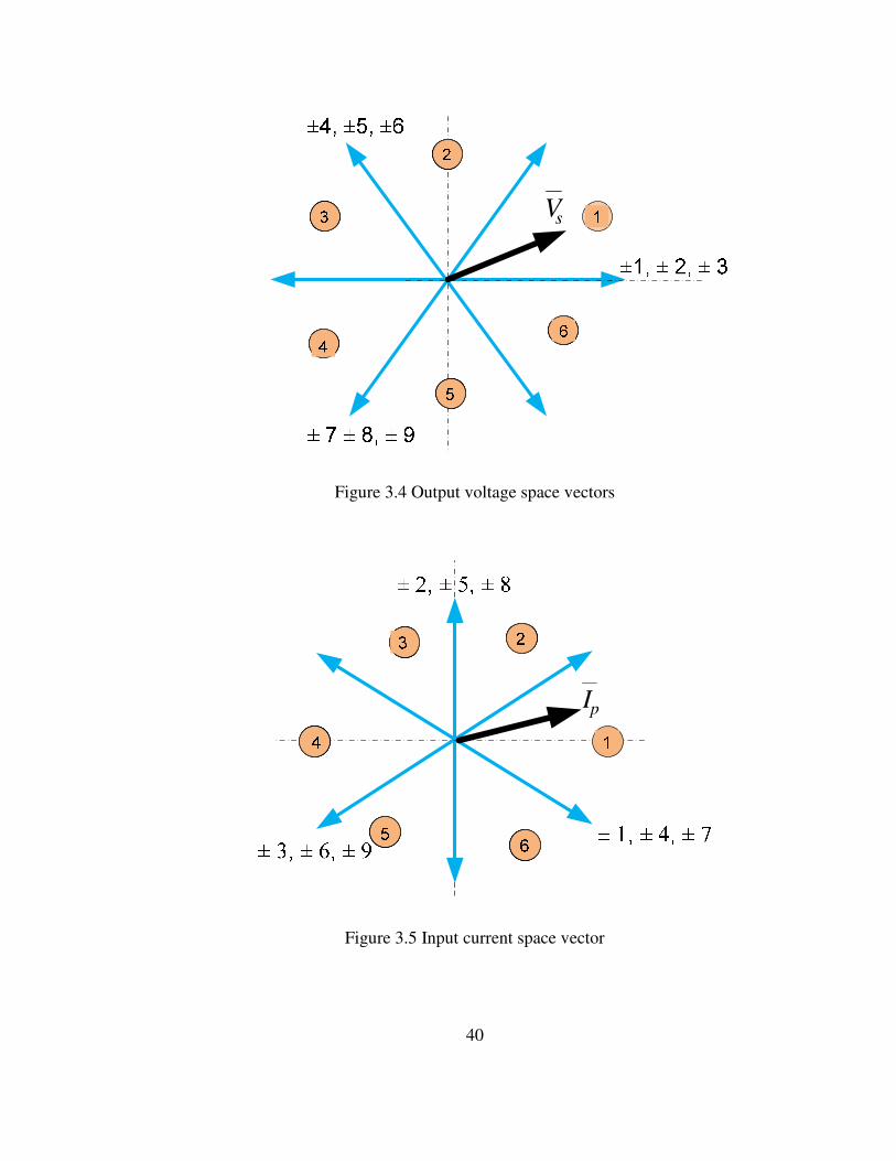
40
sV
Figure 3.4 Output voltage space vectors
pI
Figure 3.5 Input current space vector

41
Table 3.4 The Selected switching configurations for the possible sector combinations
sV
''sV
'sV
sV
''sVoα'
sV
oαπ
+6
oαπ
−6
bcVV3
22 =
caVV3
21 −=
capVV3
24 =
bcpVV3
23 −=
oαπ
−6
oαπ
+6
oα
Figure 3.6 Output voltage vector synthesis
Once these four states are determined, a zero switching states are applied to complete the
switching period which provides maximum output to input voltage transfer ratio. The
expressions for the normalized times (duty cycles) can be done by considering the
synthesis of output desired voltage and input current phase angle. Consider the input
current angle lie on sector 5 and the desired output voltage on sector 3. The selected
switching configuration is -5 +6 +8 -9 based on Table 3.4.
In switching state -5, the output voltage and input current space vectors V1 and 11
are found in Table 3.3 as
1 +9 -7 -3 +1 -6 +4 +9 -7 +3 -1 -6 +4 -9 +7 +3 -1 +6 -4 -9 +7 -3 +1 +6 -4
2 -8 +9 +2 -3 +5 -6 -8 +9 -2 +3 +5 -6 +8 -9 -2 +3 -5 +6 +8 -9 +2 -3 -5 +6
3 +7 -8 -1 +2 -4 +5 +7 -8 +1 -2 -4 +5 -7 +8 +1 -2 +4 -5 -7 +8 -1 +2 +4 -5
4 -9 +7 +3 -1 +6 -4 -9 +7 -3 +1 +6 -4 +9 -7 -3 +1 -6 +4 +9 -7 +3 -1 -6 +4
5 +8 -9 -2 +3 -5 +6 +8 -9 +2 -3 -5 +6 -8 +9 +2 -3 +5 -6 -8 +9 -2 +3 +5 -6
6 -7 +8 +1 -2 +4 -5 -7 +8 -1 +2 +4 -5 +7 -8 -1 +2 -4 +5 +7 -8 +1 -2 -4 +5
t1 t2 t3 t4 t1 t2 t3 t4 t1 t2 t3 t4 t1 t2 t3 t4 t1 t2 t3 t4 t1 t2 t3 t4Times
In p
ut
Cu
rren
t
Vec
tor
Sec
tor
Sector of output voltage vector
1 2 3 4 5 6

42
23
2
3
2
3
2
33
2
1
1
π
ππ
−∠=
∠−=−∠=
bs
bcpbcp
II
VVV
And the voltage and current space vectors in mode +6, V2 and I2 are
3
4
3
2
3
2
3
2
2
2
π
π
∠=
∠=
bs
cap
II
VV
V3 and I3 corresponding with output voltage and input current vectors in switching state
+8 are
23
2
33
2
3
4
3
2
3
3
π
ππ
−∠=
∠−=∠=
cs
bcpbcp
II
VVV
The fourth output voltage and input current vectors V4 and I4 at switching mode -9 are
3
4
3
2
33
2
4
4
π
π
∠=
∠=
cs
cap
II
VV
Since each adjacent vectors are synthesized from two voltage vectors having the same
directions.
43
''
21
'
VVV
VVV
s
s
+=
+=
(3.22)

43
iβ
iβπ
−6
iβπ
+6
iβ
pI
iβπ
−6
iβπ
+6
'pI
''pI
Figure 3.7 Input current vector synthesis
Define the two local angles which are measured from the bisection line of the sectors; αo
the angle of desired voltage measured from the bisection line of the voltage sectors and βi
the angle of input current measured from the bisection line of the current sectors.
Applying sine rule on Figure 3.6 result in one of the relation between duty ratios t1 and t2
in terms of the output and input voltages.
)3
2sin()
6sin(
'
πα
πs
o
s VV=
+
)6
sin(3
2
3
2
3
221 osbcca VtVtV α
π+=+− (3.23)
Using the same sine law on the input current vector shown in Figure 3.7, another
relationship between the duty cycles t1 and t2 is obtained as given in 3.24. It is very
interesting to note that the output current magnitude does not show up the equation.

44
Therefore, it can be concluded that the duty cycles for each switching configurations does
not depend on the magnitude of the output current rather it depends on the desired output
voltage, input voltage, input current angle and output voltage angle.
)6
sin(
3
2
)6
sin(
3
221
i
bs
i
bs tItI
βπ
βπ
−
=
+
12
)6
sin(
)6
sin(
tt
i
i
βπ
βπ
+
−= (3.24)
Solving (3.23) and (3.24) simultaneously gives the expression of t1 as follows
)6
sin(3
2)
6sin(
3
2
)6
sin()6
sin(3
2
1
ibcica
ios
VV
V
t
βπ
βπ
βπ
απ
−++−
++
=
Simplifying the denominator, and define the output voltage transfer ratio q = Vs/Vp
)cos(3
)6
sin()6
sin(2
1φ
βπ
απ
ioq
t
++=
Where Φ denotes the input power factor angle and using a trigonometric property, the
sine term can be replaced by the cosine and the final expression for t1 can be given as
)cos(3
)3
cos()3
cos(2
1φ
πβ
πα −−
=ioq
t (3.25)
Substituting back the expression (3.25) into (3.24), the duty cycle t2 is

45
)cos(3
)3
cos()3
cos(2
2φ
πβ
πα +−
=ioq
t (3.26)
Similarly, using the other adjacent voltage vector, the normalized time t3 and t4 can easily
be computed. t5 is the duty cycles for the zero switching state and the expressions of these
times are given as
)cos(3
)3
cos()3
cos(2
3φ
πβ
πα −+
=ioq
t (3.27)
)cos(3
)3
cos()3
cos(2
4φ
πβ
πα ++
=ioq
t (3.28)
43215 1 ttttt −−−−= (3.29)
3.3.2 Indirect Space Vector modulation
3.3.2.1 Space Vector for Rectifier Stage. This modulation technique applies the well
developed PWM strategies of converters to a matrix converter modulation algorithm. The
objective is still the same as the direct space vector; synthesize the output voltages
vectors from the input voltages and the input current vector from the output currents.
However, the output voltage and input current are controlled independently in indirect
space vector modulation [6].

46
Figure 3.8 Equivalent circuit for indirect matrix converter
The advantage of this modulation scheme is that it is easier to implement the well
established PWM converters modulation to the matrix converter. Besides, it is potentially
possible to directly implement PWM inverter based controller such as vector control for
induction machine, to the matrix converter [6].
As the matrix converter can equivalently represent as inverter and rectifier stages
spitted by a fiction dc link. As seen in Figure 3.8, both the rectifier and inverter power
stages consist of 6 switches.
The input current can be expressed as the virtual dc link current and the rectifier stage
switching states. Similarly, the virtual DC link voltage is mapped with the input three
phase voltages as given in (3.31).

47
Table 3.5: Truth table for rectifier stage
=
−
+
DC
DC
cnRcpR
bnRbpR
anRapR
cp
bp
ap
I
I
SS
SS
SS
I
I
I
(3.30)
=
−
+
cp
bp
ap
cnRbnRanR
cpRbpRapR
DC
DC
V
V
V
SSS
SSS
V
V (3.31)
To comply with Kirchhoff’s voltage and current laws on the rectifier stage, only one
switch from the three top switches (SapR, SbpR and ScpR) and one from the bottom switches
(SapR, SbpR and ScpR) can be turned ON simultaneously. The possible nine switching
combinations in which three of them gives zero input current and the other six gives non-
zero input current as shown in Table 3.5.
Mode Vector On Devices Iap Ibp Icp Iqp Idp Ip βp VDC
1. I 6 S apR S bnR I DC -I DC 0 I DC 1/√3I DC 2/√3I DC -π/6 V abp
2. I 1 S apR S cnR I DC 0 -I DC I DC -1/√3I DC 2/√3I DC π/6 -V cap
3. I 3 S bpR S anR -I DC I DC 0 -I DC -1/√3I DC 2/√3I DC 5π/6 -V abp
4. I 2 S bpR S cnR 0 I DC -I DC 0 -1/√3I DC 2/√3I DC π/2 V bcp
5. I 4 S cpR S anR -I DC 0 I DC -I DC 1/√3I DC 2/√3I DC -5π/6 V cap
6. I 5 S cRp S bnR 0 -I DC I DC 0 1/√3I DC 2/√3I DC -π/2 -V bcp
7. 0 I1 S apR S anR 0 0 0 - - - - -
8. 0 I2 S bpR S bnR 0 0 0 - - - - -
9. 0 I3 S cpR S cnR 0 0 0 - - - - -

48
pI
Figure 3.10 Rectifier current space vector
The input currents space vectors can be determined using a stationary qdo
transformation. The complete derivation of the input current space vectors shown in
Table 3.5 is given in Appendix III
−
−−
=
cp
bp
ap
op
dp
qp
I
I
I
I
I
I
2
1
2
1
2
12
3
2
30
2
1
2
11
3
2 (3.32)
Using (3.32), the q- and d- axis components of the input current space vector is given as
( )
( )bpcpdp
cpbpapqp
III
IIII
−=
−−=
3
1
23
2
(3.33)

49
The magnitude and the angle of the input current space vectors can be determined from
(3.34)
−=
+=
−
qp
dp
qdp
dpqpqdp
I
I
III
1
22
tanθ (3.34)
Consider the following sector to synthesize the desired input current using the two
adjacent vectors as seen in Figure 3.9. θV is the angle of desired current measured from
the lower adjust voltage vector and θI is the angle of desired current measured from the
lower adjust current.
In Figure 3.9, the reference current can be expressed as the sum of the products of the
duty cycles with the respective current space vector.
bbaaref ItItI += (3.35)
From the sine law,
)3
2sin()
3sin(
πθ
πref
I
aaIIt
=
− (3.36)
The duty cycle ta can be expressed as (3.37) using (3.36) and substituting the value of Ia
from Table 3.5.
)3
sin( IIa qt θπ
−= (3.37)
Where the current modulation index qI as follows
DC
ref
II
Iq =

50
bI
aIIθ
refI
aaIt
bbIt
Figure 3.9 Diagram for synthesis of the reference current
Similarly, applying sine laws to get a relation for duty cycle tb,
)3
2sin(
)sin( πθref
I
bbIIt
= (3.38)
And substituting the value of Ib from the Table 3.5
)sin(3
2Irefbb IIt θ=
)sin( IIb qt θ= (3.38)
The rest time will be allocated for the three zero vectors such that,
baI ttt −−=10 (3.39)

51
3.3.2.2 Space Vector for Inverter Stage. The output three phase voltages can be written
in terms of the virtual dc voltage and the switching functions. Using the switching state of
the inverter stages, the output voltages are related with the virtual dc voltage as follows.
Table 3.6 gives the complete truth table for this stage.
=
+
+
DC
DC
cnRcpR
bnRbpR
anRapR
cs
bs
as
V
V
SS
SS
SS
V
V
V
(3.40)
And the mapping between the input virtual dc link current and the output current can be
done using the same switching state transfer matrix.
=
+
+
cs
bs
as
cnRbnRanR
cpRbpRapR
DC
DC
I
I
I
SSS
SSS
I
I
(3.41)
To make the analysis more convenient the output voltages can be expressed by using only
the top devices as given in (3.42).
( )
( )
( )cpIbpIapI
DC
cs
cpIbpIapI
DC
bs
cpIbpIapI
DC
as
SSSV
V
SSSV
V
SSSV
V
23
23
23
+−−=
−+−=
−−=
(3.42)
Using stationary reference frame transformation, the q-axis and d-axis output voltage
vectors are expressed as:
( )
( )bscsds
cpIbpIapI
DC
qs
VVV
SSSV
V
−=
−−=
3
1
23
(3.43)

52
The expressions for the magnitude and angle of the voltage space vector for the inverter
stage are given as:
Table 3.6 Truth table of inverter
−=
+=
−
qs
ds
s
dsqss
V
V
VVV
1
22
tanα (3.44)
As shown in Figure 3.12, the desired output voltage is synthesized using the same space
vector modulation used in voltage source converter. θv is the angle of desired voltage
measured from the lower adjust voltage vector and
Since the reference output voltage are produced using the adjacent two vectors, it can be
expressed as the sum of the duty cycles multiplied by the respective voltage vector.
ddccref VtVtV += (3.45)
Using sine law,
)3
2sin()
3sin(
πθ
πref
V
ccVVt
=
−
Mode Vector SapI SbpI ScpI Vas Vbs Vcs Vqs Vds Vs αs IDC
1. 0 V1 0 0 0 0 0 0 - - - - -
2. V 4 0 0 1 -1/3V DC -1/3V DC 2/3V DC -1/3V DC 1/√3V DC 2/3V DC -2π/3 I cs
3. V 2 0 1 0 -1/3V DC 2/3V DC -1/3V DC -1/3V DC -1/√3V DC 2/3V DC 2π/3 I bs
4. V 3 0 1 1 -2/3V DC 1/3V DC 1/3V DC -2/3V DC 0 2/3V DC π -I as
5. V 6 1 0 0 2/3V DC -1/3V DC -1/3V DC 2/3V DC 0 2/3V DC 0 I as
6. V 5 1 0 1 1/3V DC -2/3V DC 1/3V DC 1/3V DC 1/√3V DC 2/3V DC -π/3 I bs
7. V 1 1 1 0 1/3V DC 1/3V DC -2/3V DC 1/3V DC -1/√3V DC 2/3V DC π/3 I cs
8. 0 V2 1 1 1 0 0 0 - - - - -

53
)3
sin(3
2V
c
ref
cV
Vt θ
π−=
sV
Figure 3.11 Inverter voltage space vector
dV refV
Vθ
aaVt
bbVt
dV
Figure 3.12 Diagram for synthesis of the reference voltage
Substituting the value of Vc
)3
sin(3)3
sin(
3
23
2)
3sin(
3
2V
DC
ref
V
DC
ref
V
c
ref
cV
V
V
V
V
Vt θ
πθ
πθ
π−=−=−=

54
Define a voltage modulation index qv as DC
ref
vV
Vq =
DCc VV3
2=
The duty cycle tc can be expressed as
)3
sin(3 VVc qt θπ
−= (3.46)
Similarly,
)3
2sin(
)sin( πθref
V
ddIVt
=
And the duty cycle to the other adjacent voltage is given in (3.47)
)sin(3 VVd qt θ= (3.47)
The rest time is allocated for the two zero vectors
dcV ttt −−=10 (3.48)
3.3.2.3 Indirect Space Vector for Matrix Converter. Using two space vectors derived
in the previous sections, the matrix converter output voltage space vectors can be
obtained using the inverter stage space vectors. And the input current space vector of the
matrix converter is synthesized employed using the rectifier power stage space vectors.
The four normalized times for the entire matrix converter is computed using the
product of the duty cycles of rectifier and inverter stages.

55
)3
sin()3
sin(3
)sin()3
sin(3
)3
sin()sin(3
)sin()sin(3
4
3
2
1
IVIVca
IVIVcb
IVIVda
IVIVdb
qqttt
qqttt
qqttt
qqttt
θπ
θπ
θθπ
θπ
θ
θθ
−−==
−==
−==
==
(3.49)
Applying power balance equations in the rectifier stage
inCSRoutCSR PP = (3.50)
The output power of the rectifier is
DCDCoutCSR IVP = (3.51)
And the input three phase power is given (3.52)
)cos(2
3φppinCSR IVP = (3.52)
Where φ is the input power factor angle and Vp is peak of the input voltage
)cos(2
3φrefpDCDC IVIV = (3.53)
The product qvqI can be evaluated as:
DCdc
refref
DC
ref
dc
ref
IVIV
IV
I
I
V
Vqq == (3.54)
Using (3.53) and (3.54)
)cos(3
2
)cos(2
3 φφ p
ref
refp
refref
IVV
V
IV
IVqq == (3.55)
Define q as the ratio of the output voltage to the input voltage,
p
ref
V
Vq =

56
(3.55) can be expressed in terms of the voltage ratio as follows
)cos(3
2
φ
qqq II = (3.56)
Substituting (3.56) into (3.49),
)cos(3
)sin()sin(2)sin()sin(
)cos(3
23)sin()sin(31
φ
θθθθ
φθθ IV
IVIVIV
qqqqt =
==
The expressions for the first active duty cycles are given in (3.57).
)cos(3
)3
sin()3
sin(2
)cos(3
)sin()3
sin(2
)cos(3
)3
sin()sin(2
)cos(3
)sin()sin(2
4
3
2
1
φ
θπ
θπ
φ
θθπ
φ
θπ
θ
φ
θθ
IV
IV
IV
IV
q
t
q
t
q
t
qt
−−=
−=
−=
=
(3.57)
And the normalized time for the zero vectors is,
43215 1 ttttt −−−−= (3.58)
To compare the results of the direct and indirect space vector modulation techniques,
define two angles αo and βi. αo is the angle of desired voltage measured from the bisection
line of the voltage sectors, βi is the angle of input current measured from the bisection
line of the current sectors. And it is stated that θv is the angle of desired voltage measured
from the lower adjust voltage vector and θI is the angle of desired current measured from
the lower adjust voltage vector. It is possible to relate the two sets of angles as follows.

57
6
6
πβθ
παθ
+=
+=
iI
oV
(3.59)
Therefore, the expressions for the duty cycles in terms of the local angles is given in
(3.60)
)cos(3
)3
cos()3
cos(2
)cos(3
)3
cos()3
cos(2
)cos(3
)3
cos()3
cos(2
)cos(3
)3
cos()3
cos(2
4
3
2
1
φ
πβ
πασ
φ
πβ
πασ
φ
πβ
πασ
φ
πβ
πασ
++=
−+=
+−=
−−=
io
io
io
io
t
t
t
t
(3.60)
43215 1 ttttt −−−−= (3.61)
Comparing the results given above with (3.25) to (3.29), it can be concluded that
both direct and indirect space vector modulation ultimately result in the same expression
for the duty cycles.
Based on the two stages space vector modulations, the current and voltage vectors
for the whole six sectors are shown in Table 3.7. To synthesize each input current and
output voltage vectors, two adjacent vectors are required. Therefore, there are four
vectors used to synthesize both vectors.

58
Table 3.7 Modes for voltage and current sectors
Table 3.8 Switching configuration for the combined matrix
Table 3.9 Modes result in zero voltage and current vectors
Since each space vectors consists of 6 sectors, there are 36 input current and
output voltage sector combinations. These are shown in Table 3.8, which has the same
switching configuration derived based on direct space vector modulation and given in
Table 3.4.
V1 V2 V3 V4 V5 V6
I1 AAC CAC CAA CCA ACA ACC
I2 BBC CBC CBB CCB BCB BCC
I3 BBA ABA ABB AAB BAB BAA
I4 CCA ACA ACC AAC CAC CAA
I5 CCB BCB BCC BBC CBC CBB
I6 AAB BAB BAA BBA ABA ABB
1 2 3 4 5 6
V1 , V6 V2 , V1 V3 , V2 V4 , V3 V5 , V4 V6 , V5
1 I1, I6 AAC, AAB, ACC, ABB CAC, BAB, AAC, AAB CAA, BAA, CAC, BAB CCA, BBA, CAA, BAA ACA, ABA, CCA, BBA ACC, ABB, ACA, ABA
+9, -7, -3, +1 -6, +4, +9, -7 +3, -1, -6, +4 -9, +7, +3, -1 +6, -4, -9, +7 -3, +1, +6, -4
2 I2, I1 BBC, AAC, BCC, ACC CBC, CAC, BBC, AAC CBB, CAA, CBC, CAC CCB, CCA, CBB, CAA BCB, ACA, CCB, CCA BCC, ACC, BCB, ACA
-8, +9, +2, -3 +5, -6, -8, +9 -2, +3, +5, -6 +8, -9, -2, +3 -4, +5, +7, -8 +1, -2, -4, +5
3 I3, I2 BBA, BBC, BAA, BCC ABA, CBC, BBA, BBC ABB, CBB, ABA, CBC AAB, CCB, ABB, CBB BAB, BCB, AAB, CCB BAA, BCC, BAB, BCB
+7, -8, -1, +2 -4, +5, +7, -8 +1, -2, -4, +5 -7, +8, +1, -2 +4, -5, -7, +8 -1, +2, +4, -5
4 I4, I3 CCA, BBA, CAA, BAA ACA, ABA, CCA, BBA ACC, ABB, ACA, ABA AAC, AAB, ACC, ABB CAC, BAB, AAC, AAB CAA, BAA, CAC, BAB
-9, +7, +3, -1 +6, -4, -9, +7 -3, +1, +6, -4 +9, -7, -3, +1 -6, +4, +9, -7 +3, -1, -6, +4
5 I5, I4 CCB, CCA, CBB, CAA BCB, ACA, CCB, CCA BCC, ACC, BCB, ACA BBC, AAC, BCC, ACC CBC, CAC, BBC, AAC CBB, CAA, CBC, CAC
+8, -9, -2, +3 -4, +5, +7, -8 +1, -2, -4, +5 -8, +9, +2, -3 +5, -6, -8, +9 -2, +3, +5, -6
6 I6, I5 AAB, CCB, ABB, CBB BAB, BCB, AAB, CCB BAA, BCC, BAB, BCB BBA, BBC, BAA, BCC ABA, CBC, BBA, BBC ABB, CBB, ABA, CBC
-7, +8, +1, -2 +4, -5, -7, +8 -1, +2, +4, -5 +7, -8, -1, +2 -4, +5, +7, -8 +1, -2, -4, +5
0V1 0V2
0I1 AAA AAA
0I2 BBB BBB
0I3 CCC CCC

59
Table 3.10 Sequence of switching devices
Table 3.8 shows only the four active vectors, but in actual switching sequence the three
zero vectors are included sequence. It can notice that these zero vectors are added at the
two ends and in the middle of the sequence. For example the sequence when both input
current and output voltage vectors lie on sector I, the sequence which result in the
minimum switching transition is shown as
CCC -> ACC -> AAC -> AAA -> AAB -> ABB -> BBB
It is necessary to note that the middle zero vectors do not show in Table 3.10. AAA is
added in the middle of the sequences of the first and fourth row; whereas BBB on third
and six rows and CCC on the second and fifth rows. The complete procedure of finding
the actual devices selected to construct Table 3.10 for all the possible output voltage and
input current space vector combinations are presented in Appendix D.
1 2 3
V1 ,V6 V2 ,V1 V3 ,V2
1 I1 ,I6 CCC, ACC, AAC, AAB, ABB, BBB BBB, BAB, AAB, AAC, CAC, CCC CCC, CAC, CAA, BAA, BAB, BBB
2 I2 ,I1 BBB, BBC, BCC, ACC, AAC, AAA AAA, AAC, CAC, CBC, BBC, BBB BBB, CBB, CBC, CAC, CAA, AAA
3 I3 ,I2 AAA, BAA, BBA, BBC, BCC, CCC CCC, CBC, BBC, BBA, ABA, AAA AAA, ABA, ABB, CBB, CBC, CCC
4 I4 ,I3 CCC, CCA, CAA, BAA, BBA, BBB BBB, BBA, ABA, ACA, CCA, CCC CCC, ACC, ACA, ABA, ABB, BBB
5 I5 ,I4 BBB, CBB, CCB, CCA, BAA, AAA AAA, ACA, CCA, CCB, BCB, BBB BBB, BCB, BCC, ACC, ACA, AAA
6 I6 ,I5 AAA, AAB, ABB, CBB, CCB, CCC CCC, CCB, BCB, BAB, AAB, AAA AAA, BAA, BAB, BCB, BCC, CCC
4 5 6
V4 ,V3 V5 ,V4 V6 ,V5
1 I1 ,I6 CCC, CCA, CAA, BAA, BBA, BBB BBB, BBA, ABA, ACA, CCA, CCC CCC, ACC, ACA, ABA, ABB, BBB
2 I2 ,I1 BBB, CBB, CCB, CCA, BAA, AAA AAA, ACA, CCA, CCB, BCB, BBB BBB, BCB, BCC, ACC, ACA, AAA
3 I3 ,I2 AAA, AAB, ABB, CBB, CCB, CCC CCC, CCB, BCB, BAB, AAB, AAA AAA, BAA, BAB, BCB, BCC, CCC
4 I4 ,I3 CCC, ACC, AAC, AAB, ABB, BBB BBB, BAB, AAB, AAC, CAC, CCC CCC, CAC, CAA, BAA, BAB, BBB
5 I5 ,I4 BBB, BBC, BCC, ACC, AAC, AAA AAA, AAC, CAC, CBC, BBC, BBB BBB, CBB, CBC, CAC, CAA, AAA
6 I6 ,I5 AAA, BAA, BBA, BBC, BCC, CCC CCC, CBC, BBC, BBA, ABA, AAA AAA, ABA, ABB, CBB, CBC, CCC

60
Table 3.11 Neutral voltage in output voltage Sector I and input current sector II
3.3.3 Common Mode Voltage Expression Based on Duty Cycle Space Vector
Modulation
An efficient mathematical approach for the analysis of matrix converter
modulation techniques are developed based on a duty-cycle space vector [26]. This
method uses the instantaneous space vector modulation. Consider a three phase time
varying waveforms xa, xb and xc. Transformed qd axis with a stationary reference frame
transformation given in (3.62).
=
c
b
a
o
d
q
x
x
x
x
x
x
2
1
2
1
2
13
4sin
3
2sin0
3
4cos
3
2cos1
3
2 ππ
ππ
(3.62)
From (3.62), xq, xd and xo can be expressed as
+
+=
3
4cos
3
2cos
3
2 ππcbaq xxxx (3.63)
Vas Vbs Vcs Vno
+9 AAC Vap Vap Vcp Vno1
-7 AAB Vap Vap Vbp Vno2
-3 ACC Vap Vcp Vcp Vno3
+1 ABB Vap Vbp Vbp Vno4
AAA Vap Vap Vap Vno5
BBB Vbp Vbp Vbp Vno6
CCC Vcp Vcp Vcp Vno7
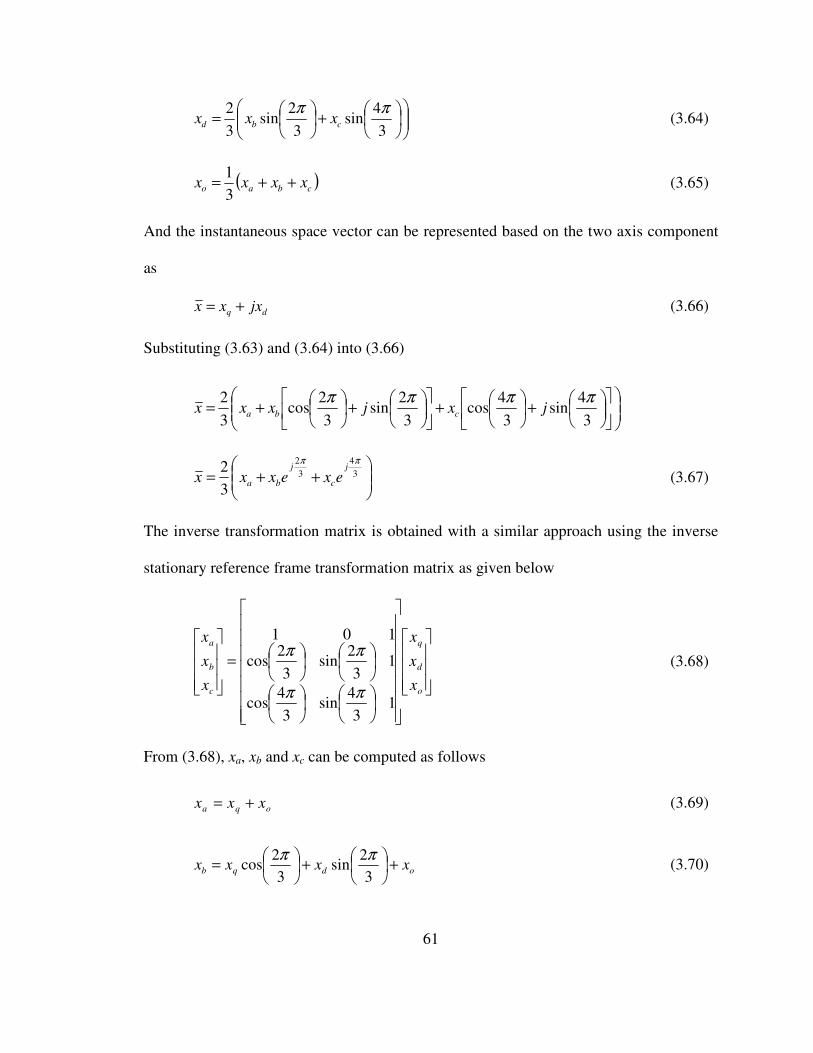
61
+
=
3
4sin
3
2sin
3
2 ππcbd xxx (3.64)
( )cbao xxxx ++=3
1 (3.65)
And the instantaneous space vector can be represented based on the two axis component
as
dq jxxx += (3.66)
Substituting (3.63) and (3.64) into (3.66)
+
+
+
+=
3
4sin
3
4cos
3
2sin
3
2cos
3
2 ππππjxjxxx cba
++= 3
4
3
2
3
2ππ
j
c
j
ba exexxx (3.67)
The inverse transformation matrix is obtained with a similar approach using the inverse
stationary reference frame transformation matrix as given below
=
o
d
q
c
b
a
x
x
x
x
x
x
13
4sin
3
4cos
13
2sin
3
2cos
101
ππ
ππ (3.68)
From (3.68), xa, xb and xc can be computed as follows
oqa xxx += (3.69)
odqb xxxx +
+
=
3
2sin
3
2cos
ππ (3.70)

62
odqc xxxx +
+
=
3
4sin
3
4cos
ππ (3.71)
Since xq is expressed as the dot product of the space vector x with the unit vector in the
direction of zero axis.
0j
q exx ⋅= (3.72)
And the xd is give as the dot product of the space vector x with the unity vector in the
direction of 90o.
2
πj
d exx ⋅= (3.73)
Substituting (12) into (9)
o
j
a xexx +⋅= 0 (3.74)
And substituting (12) and (13) into (10)
o
jj
b xeexx +
+
⋅=
3
2sin
3
2cos 20 ππ
π
o
j
b xexx +⋅= 3
2π
(3.75)
Similarly substituting (12) and (13) into (11),
o
j
c xexx +⋅= 3
4π
(3.76)
Therefore, the space vector can be represented using the following transformation
( )cbao
j
c
j
ba
xxxx
exexxx
++=
++=
3
1
3
23
4
3
2 ππ
(3.77)

63
And the inverse transformation leads to
o
j
c
o
j
b
o
j
a
xexx
xexx
xexx
+⋅=
+⋅=
+⋅=
3
4
3
2
0
π
π
(3.78)
In direct duty-cycle methods, instead of defining switching matrix, averaged matrix can
be directly constructed from the known input voltage and output current and desired
output voltage and input current [26, 37].
==
cCbCaC
cBbBaB
cAbAaA
ijij
MMM
MMM
MMM
SaveM )( (3.79)
In order to prevent short circuit on the input side and ensure continuous output current
=++
=++
=++
≤
1
1
1
1
cCbCaC
cBbBaB
cAbAaA
ij
MMM
MMM
MMM
M
(3.80)
Based on the transformation given in (3.77), the first three duty cycles in the first the
matrix given in (17) can be represented by the duty-cycle space vector as follows
( ))3/4()3/2(
3
2 ππ j
cA
j
bAaAA eMeMMM ++= (3.81)
( ))3/4()3/2(
3
2 ππ j
cB
j
bBaBB eMeMMM ++= (3.82)
( ))3/4()3/2(
3
2 ππ j
cC
j
bCaCC eMeMMM ++= (3.83)
And the inverse transformation can be obtained based on (3.78.) and the constraint given
in (3.80)

64
)3/4(
)3/2(
0
3
1
3
1
3
1
π
π
j
AcA
j
AbA
j
AaA
eMM
eMM
eMM
⋅+=
⋅+=
⋅+=
(3.84)
Similarly, the second row on the matrix given in (3.79) can be obtained using the inverse
transformation as
)3/4(
)3/2(
0
3
1
3
1
3
1
π
π
j
BcB
j
BbB
j
BaB
eMM
eMM
eMM
⋅+=
⋅+=
⋅+=
(3.85)
Finally, the inverse transformation corresponding to the third row can be given as
)3/4(
)3/2(
0
3
1
3
1
3
1
π
π
j
CcC
j
CbC
j
CaC
eMM
eMM
eMM
⋅+=
⋅+=
⋅+=
(3.86)
The input/output relationship of voltages and currents are related to the states of the nine
averaged switches and represented as
=
cp
bp
ap
cCbCaC
cBbBaB
cAbAaA
cs
bs
as
V
V
V
MMM
MMM
MMM
V
V
V
(3.87)
=
cs
bs
as
T
cCbCaC
cBbBaB
cAbAaA
cp
bp
ap
I
I
I
MMM
MMM
MMM
I
I
I
(3.88)

65
Transforming the output three phase voltages to space vector using (3.77)
++= 3
4
3
2
3
2ππ
j
cs
j
bsass eVeVVV (3.89)
Substituting (3.87) into (3.89)
++
+++
+++
=
3
4
3
2
)(
)(
)(
3
2
π
π
j
cpcCbpbCapaC
j
cpcBbpbBapaB
cpcAbpbAapaA
s
eVMVMVM
eVMVMVM
VMVMVM
V (3.90)
The input three phase capacitor voltages can be represented in the terms of the input
voltage space vector using the inverse transformation given in (3.78) for a balance
voltage sets.
3
4
3
2
0
π
π
j
pcp
j
pbp
j
pap
eVV
eVV
eVV
⋅=
⋅=
⋅=
(3.91
Substituting (3.91), (3.84), (3.85) and (3.86) into (3.90),
)(2
)(2
3
4
3
2*
3
4
*3
2
**
ππππj
C
j
BA
pj
B
j
BA
p
s eMeMMV
eMeMMV
V +++++= (3.92)
Similarly, the input currents are transformed to instantaneous space vector
++= 3
4
3
2
3
2ππ
j
cp
j
bpapp eIeIII (3.93)

66
From (3.93) and (3.88)
++
+++
+++
=
3
4
3
2
)(
)(
)(
3
2
π
π
j
cscCbscBascA
j
csbCbsbBasbA
csaCbsaBasaA
p
eIMIMIM
eIMIMIM
IMIMIM
I (3.94)
Using the inverse transformation, the output current can be given in terms of the output
current space vector as follows.
3
4
3
2
0
π
π
j
scs
j
sbs
j
sas
eII
eII
eII
⋅=
⋅=
⋅=
(3.95)
Substituting (3.95), (3.84), (3.85) and (3.86)
)(2
)(2
3
2
3
4*
3
4
3
2 ππππj
C
j
BA
sj
C
j
BA
s
p eMeMMI
eMeMMI
I +++++= (3.96)
From (3.92) and (3.96), the following three vectors can be introduced
++= 3
4
3
2
3
1ππ
j
C
j
BAD eMeMMM (3.97)
++= 3
2
3
4
3
1ππ
j
C
j
BAI eMeMMM (3.98)
( )CBA MMMM ++=3
10 (3.99)
The three vectors, DM , IM and oM might be considered as a direct, inverse and zero
components of the duty-cycle space vector.

67
AM , BM and CM can be computed using the inverse transformation of (3.97) –
(3.99).
( )OIDA MMMM ++=3
1 (3.100)
++= O
j
I
j
DB MeMeMM 3
2
3
4
3
1ππ
(3.101)
++= O
j
I
j
DC MeMeMM 3
4
3
2
3
1ππ
(3.102)
Substituting (3.100)-(3.102) into (3.92)
DpIps MVMVV**
2
3
2
3+= (3.103)
Substituting (3.100)-(3.102) into (3.96)
DsIsp MIMII*
2
3
2
3+= (3.104)
In a space vector modulation of a matrix converter, it is possible to control the output
voltage space vector and the input current direction (or the input power factor). Note that
it is not possible to control the magnitude of the input current. (3.106) is obtained by
imposing the vector DsIs MIMI *+ in the direction of the input current space vector [21,
26]. Therefore, the dot product of this vector with a unit vector perpendicular to the input
current phase angle is zero.
DpIps MVMVV**
2
3
2
3+= (3.105)

68
ϕjMIMI DsIs ⋅+= )(0 * (3.106)
ϕ is defined as a unit vector in direction of the input current space vector.
The solution for DM and IM is given in (3.107) and (3.108). The parameter λ is
a real variable which reflects the degree of freedom which can be used to define different
type of modulation strategy.
**)(3 spp
sD
IVV
VM
λ
ϕ
ϕ+
⋅= (3.107)
**
*
)(3 spp
sI
IVV
VM
λ
ϕ
ϕ−
⋅= (3.108)
The vectors in (3.107) and (3.108) can be written in polar form as follows
ip
is
vp
vs
j
pp
j
ss
j
pp
j
ss
eII
eII
eVV
eVV
θ
θ
θ
θ
=
=
=
=
(3.109)
Where ipθ and vp
θ is the input current and voltage angles. vsθ and is
θ are the output
voltage and current, respectively. The output displacement angle, isvss θθϕ −= . The
voltage transfer ration is represented by q.
Substituting (3.109) into (3.107) and (3.109),
))(1(3
1 )(jreqeM svsvp jj
D −+= −+γϕθθ
(3.110)

69
))(1(3
1 )(jreqeM svsvp jj
I +−= −−γϕθθ
(3.111)
where
ss
spIV
λϕϕγ
3sintan += (3.112)
spr ϕϕ costan= (3.113)
ipvpp θθϕ −= (3.114)
From (3.100) to (3.102) the duty cycle space vector can be determined by adding an
appropriate zero sequence components.
ojIjDij MMMM ++= αα * (3.115)
where the unity vector jα can be given as.
=
=
=
=
Cje
Bje
Aj
j
j
j
,
,
,1
)3/4(
)3/2(
π
πα (3.116)
The duty cycle can be determined based on (3.115) and using the inverse transformation
given in (3.78). It can be observed that ijM is a duty cycle and it is a scalar term whereas
the duty cycle space vector, ijM is a vector quantity.
kijij MM α⋅+=3
1 (3.117)
Substituting (3.115) into (3.117), the expression for the duty cycles becomes

70
kojIjDij MMMM ααα ⋅+++= )(
3
1 *
kjIjDkoij MMMM αααα ⋅++⋅+= )(
3
1 * (3.118)
It is necessary to note that, the duty cycle is a scalar terms since it is the result of the dot
products of two vectors as seen in (3.118). In addition, it can also be expressed as a sum
of two scalars as follows.
ijojij AMM += (3.119)
The first scalar term is the component of the zero sequence space vectors and it is given
as
jooj MM α⋅+=3
1 (3.120)
And the second terms which reflect the duty cycle space vector without the zero sequence
component. These components can be defined as the duty cycle resulting from the active
switching states and they are defined as
jiIiDij MMA ααα ⋅+= )( * (3.121)
It is necessary to note that the above quantities linearly depend on DM and IM ;
hence, they also depend on the output voltage transfer ratio and λ . Thus, Aij are used to
specify the parameter λ which result in the maximum output voltage transfer ratio for a
given output current angle.

71
Since the modulation signals are average of the switching functions, the feasible
value of the duty cycles is between 0 and 1. Applying this constraint on (3.119),
10 ≤+≤ ijoj AM (3.122)
It is possible to rewrite (3.122) in the following inequality,
ijojij AMA max1min −≤≤− (3.123)
Using (3.123), the following inequality holds true,
1minmax ≤− ijij AA (3.124)
For each desired output phase voltage Vref,j the corresponding three active duty cycles
used to synthesize it are Aaj, Abj and Acj. At any instant of time, the minimum and the
maximum of the three active duty cycles are defined as Aj,min and Aj,max, respectively.
cjbjajj
cjbjajj
AAAA
AAAA
,,max
,,min
max,
min,
=
= (3.125)
Substituting (3.121) into (3.124)
1)()( min
*
minmax
*
max ≤⋅+−⋅+ jIDjID MMMM αααααα
( ) 1)()( maxmax
*
min
*
max ≤⋅−+− jID MM ααααα
( ) 1* ≤⋅∆+∆ jID MM α (3.126)
where
minmax αα −=∆ (3.127)

72
Using the definition of α given in (3.116), the difference between minimum and the
maximum values are always 3 .This is demonstrated as follow,
Case 1 1max == Aαα and )3/2(
min
παα j
B e==
3
2
3
2
31 )3/2(
minmax =+=−=−=∆ je j παα
Case 2 )3/2(
max
παα j
B e== and )3/4(
min
παα j
C e==
33)3/4()3/2(
minmax ==−=−=∆ jeejj ππαα
Case 2 )3/4(
max
παα j
C e== and 1min == Aαα
3
2
3
2
31)3/4(
minmax =−−=−=−=∆ je j παα
From (3.126) the worst case is when the following scalar product is maximum.
( ) 1* ≤∆+∆ ID MM (3.128)
Substituting (3.110) and (3.111) into (3.128)
( ) )cos()sin()cos(3
2*
∆∆∆ −−−−−+−=∆+∆ θϕθγϕθθγθθ sssssID jjqMM (3.129)
Cauchy-Swartz inequality: states that for any vector x and y
22
yxyxyx +=≤+ (3.130)
Applying the property of Cauchy-Swartz inequality on (3.129),

73
221)cos()sin()cos( rjrj sssss ++≤−−−−−+− ∆∆∆ γθϕθϕθθγθθ (3.131)
Substituting (3.131) and (3.129),
( ) 22* 13
2rqMM ID ++=∆+∆ γ (3.132)
Using (3.128) and (3.132)
113
2 22 ≤++ rq γ (3.133)
It can be rewritten as
2212
3
rq
++≤
γ (3.134)
From the matrix converter maximum allowable voltage transfer ratio,
2
3≤q (3.135)
Based on (134) and (135), the condition for the maximum voltage transfer function is
give as
0=γ and 0=r (3.136)
Base on the condition given in (3.136) and substituting into (3.112), the necessary
condition to obtain the maximum voltage transfer ratio is obtained if the parameter λ has
the following value
))sin()tan(1(3
1sssp IVj ϕϕλ −−= (3.137)

74
pϕ and sϕ are the input and output power factors.
Substituting (3.137) into (3.110) and (3.111)
))cos()tan(1(3 *
sj
sp
p
sD ej
V
VM
ϕϕϕ −−= (3.138)
))cos()tan(1(3 *
sj
sp
p
sI ej
V
VM
ϕϕϕ−= (3.139)
The zero sequence components are necessary for the calculation of the duty-cycle and the
basic idea is to search the minimum among the duty cycles for each input phase.
)min( ijoj M=δ (3.140)
After the minimum duty cycle ojδ is computed, substituting (3.119) into (3.140).
)min( ijojoj AM −= δ (3.141)
Finally, the zero sequence components can be calculated as
∑=
=3
13
2
j
jojo MM α (3.142)
To summarize the duty cycle space vector, consider the desired three phase output
voltages are
)3
2cos(
)3
2cos(
)cos(
__
__
__
πθω
πθω
θω
++=
−+=
+=
ssrefsrefcs
ssrefsrefbs
ssrefsrefas
tVV
tVV
tVV

75
Space vector for the desired output voltage are found using the transformations
given in (3.77). The desired output voltage vector can be represented as refsV _ . For the
known output current angle, the output power factor can be represented as sϕ . Therefore,
DM , IM and oM for the desired output voltage and input power factor refp _ϕ under the
given output power factor can be determined as follow
Once, DM , IM and oM are determined the duty cycles can be calculated based on
))cos()tan(1(3
_*
_sj
srefp
p
refs
D ejV
VM
ϕϕϕ −−=
))cos()tan(1(3
_*
_sj
srefp
p
refs
I ejV
VM
ϕϕϕ−=
∑
=
=3
13
2
j
jojo MM α
Once the duty cycle space vectors DM , IM and oM are determined, the duty cycles of
each switch can be calculated as follows
kjIjDkoij MMMM αααα ⋅++⋅+= )(
3
1 *
jooj MM α⋅+=3
1
These expressions give the appropriate duty cycle for each switch to synthesize the
desired output voltage and input current direction (or input power factor) simultaneously.
76
3.4 Simulation Results and Discussion
Simulation has been done using the carrier based modulation techniques and using a
60 Hz of input frequency, 30 Hz output frequency and 5 kHz switching frequencies and
the results are demonstrated in Figure 3.13 to Figure 3.20.
Figure 3.13 shows the modulation signals used to generate phase ‘a’ output voltage.
This modulation signal have basically consists of the dc component, the sum of the input
and output frequencies, 90Hz and the difference between the two frequencies, 30Hz as
seen in Figure 3.14. Unlike the conventional PWM technique for converters, the
modulation signals do not directly used to generate the switching pulses rather the three
signals Z1A, Z2A and Z3A are first synthesized as seen in Figure 3.15. Since Z3A is always
unity the corresponding intermediate pulses P3A is also ON and it is not shown in Figure
3.16. This figure only show the intermediate pulses P1A and P1A generated by comparing
Z1A and Z2A, with triangle carrier.
After the intermediate signals are generated, actual switching signals are produced
using (3.15) and presented in Figure 3.17. As seen from the results, only one switch is
turned ON at each instant of time which avoids input voltage short circuit and there is a
one switch which turns ON so that a current path is always provided. With similar
approach, the modulation signals used to synthesize the output phase ‘b’ voltage are
shown in Figure 3.18 and the actual switching signal which compiles both Kirchhoff’s
laws are given in Figure 3.19. And finally Figure 3.20 and Figure 3.21 show the
modulation and actual switching signals which synthesize phase ‘c’ output voltage.

77
Figure 3.13 Modulation signals for output phase ‘a’ voltage
Figure 3.14 FFT for the modulation signal MaA
0.4 0.41 0.42 0.43 0.44 0.45 0.46 0.47 0.48 0.49 0.5
0.2
0.4
0.6
0.8
Ma
A
0.4 0.41 0.42 0.43 0.44 0.45 0.46 0.47 0.48 0.49 0.5
0.2
0.4
0.6
0.8
Mb
A
0.4 0.41 0.42 0.43 0.44 0.45 0.46 0.47 0.48 0.49 0.5
0.2
0.4
0.6
0.8
Mc
A
Time [Sec]
0 20 40 60 80 100 120 140 160 180 2000
0.1
0.2
0.3
0.4
0.5
0.6
0.7
Frequency (Hz)
Ha
rmon
ic M
ag
nit
ud
e

78
Figure 3.15 Carrier based pulse width modulation
Figure 3.16 Intermediate signals used to generate switching signals
0.4 0.405 0.41 0.415 0.42 0.425 0.43 0.435 0.44 0.445 0.45
0
0.5
1
0.3 0.3005 0.301 0.3015 0.302 0.3025 0.303 0.3035 0.304 0.3045 0.305
0
0.5
1
Time [Sec]
Z1
Z2 Z
3
0.3 0.3005 0.301 0.3015 0.302 0.3025 0.303 0.3035 0.304 0.3045 0.305
0
0.5
1
P1A
0.3 0.3005 0.301 0.3015 0.302 0.3025 0.303 0.3035 0.304 0.3045 0.305
0
0.5
1
P2A
Time [Sec]

79
Figure 3.17 Switching signals for output phase ‘a’ voltage
Figure 3.18 Modulation signals for output phase ‘b’ voltage
0.4 0.4005 0.401 0.4015 0.402 0.4025 0.403 0.4035 0.404 0.4045 0.405
0
0.5
1
SaA
0.3 0.3005 0.301 0.3015 0.302 0.3025 0.303 0.3035 0.304 0.3045 0.305
0
0.5
1
SbA
0.3 0.3005 0.301 0.3015 0.302 0.3025 0.303 0.3035 0.304 0.3045 0.305
0
0.5
1
ScA
Time [Sec]
0.4 0.41 0.42 0.43 0.44 0.45 0.46 0.47 0.48 0.49 0.5
0.2
0.4
0.6
0.8
MaB
0.4 0.41 0.42 0.43 0.44 0.45 0.46 0.47 0.48 0.49 0.5
0.2
0.4
0.6
0.8
MbB
0.4 0.41 0.42 0.43 0.44 0.45 0.46 0.47 0.48 0.49 0.5
0.2
0.4
0.6
0.8
McB
Time [Sec]

80
Figure 3.19 Switching signals for output phase ‘b’ voltage
Figure 3.20 Modulation signals for output phase ‘c’ voltage
0.4 0.4005 0.401 0.4015 0.402 0.4025 0.403 0.4035 0.404 0.4045 0.405
0
0.5
1
SaB
0.3 0.3005 0.301 0.3015 0.302 0.3025 0.303 0.3035 0.304 0.3045 0.305
0
0.5
1
SbB
0.3 0.3005 0.301 0.3015 0.302 0.3025 0.303 0.3035 0.304 0.3045 0.305
0
0.5
1
ScB
Time [Sec]
0.4 0.41 0.42 0.43 0.44 0.45 0.46 0.47 0.48 0.49 0.5
0.2
0.4
0.6
0.8
MaC
0.4 0.41 0.42 0.43 0.44 0.45 0.46 0.47 0.48 0.49 0.5
0.2
0.4
0.6
0.8
MbC
0.4 0.41 0.42 0.43 0.44 0.45 0.46 0.47 0.48 0.49 0.5
0.2
0.4
0.6
0.8
McC
Time [Sec]

81
Figure 3.21 Switching signals for output phase ‘c’ voltage
Figure 3.22 Input three phase voltages
0.4 0.4005 0.401 0.4015 0.402 0.4025 0.403 0.4035 0.404 0.4045 0.405
0
0.5
1
SaC
0.3 0.3005 0.301 0.3015 0.302 0.3025 0.303 0.3035 0.304 0.3045 0.305
0
0.5
1
SbC
0.3 0.3005 0.301 0.3015 0.302 0.3025 0.303 0.3035 0.304 0.3045 0.305
0
0.5
1
ScC
Time [Sec]
0.1 0.105 0.11 0.115 0.12 0.125 0.13 0.135 0.14 0.145 0.15
-200
0
200
Vap [
V]
0.1 0.105 0.11 0.115 0.12 0.125 0.13 0.135 0.14 0.145 0.15
-200
0
200
Vb
p [
V]
0.1 0.105 0.11 0.115 0.12 0.125 0.13 0.135 0.14 0.145 0.15
-200
0
200
Vc
p [
V]
Time [sec]

82
The modulation signals generated using the methods discussed in this chapter is
used to synthesize the desired three phase output voltage of 180V phase peak-to-peak
with a frequency of 50Hz. The input three phase voltages are 310V with a frequency of
60Hz as shown in Figure 3.22. As seen in Figure 3.23, the desired voltages are about
180V/50Hz and form balanced sets. The input power factor at the input terminal of the
matrix converter is kept high to allow wide range of voltage transfer ratio. Figure 3.24
shows the input phase ‘a’ capacitor voltage and phase ‘a’ input matrix converter current
which are in phase and hence unity input power factor operation at the input terminal.
From Figure 3.23 in particular, it can be concluded that the developed carrier-based
modulation scheme along with the technique used to generate the actual nine switching
signal perfectly synthesizes the desired output voltage.
Figure 3.23 synthesized output three phase voltages
0.1 0.11 0.12 0.13 0.14 0.15 0.16-400
-200
0
200
400
Vas [
V]
0.1 0.11 0.12 0.13 0.14 0.15 0.16-400
-200
0
200
400
Vbs [
V]
0.1 0.11 0.12 0.13 0.14 0.15 0.16-400
-200
0
200
400
Vcs [
V]
Time [sec]

83
Figure 3.24 Phase ‘a’ input capacitor voltage and input matrix converter current with
unity input power factor
3.5 Conclusion
The chapter presents both carrier-based and space vector modulation technique for
three phase-to-three phase matrix converter. The resulting expressions of the modulation
signals are simple and suitable for practical implementation. Besides, it is general that it
can be used for unbalanced input voltages. It is interesting that this technique gives the
same result as the complex and the more mathematically intensive approaches given in
[3]. Detailed methodologies for generation of switching signals are also presented. The
direct and indirect space vector modulations are clearly developed. The final result shows
that it is possible to equivalently analyze the matrix converter into rectifier and inverter
stages for the purpose of modulation and result in the same switching configuration as the
direct space vector modulation. Although the space vector modulation does not require
injection of third harmonic component, the common mode voltage is derived using space
0.1 0.105 0.11 0.115 0.12 0.125 0.13 0.135 0.14 0.145 0.15
-300
-200
-100
0
100
200
300
Time [sec]
Vap
[V] Iap
[A]

84
vector which can be implemented in carrier based modulation. Computer simulation has
also been done to verify the theoretical modulation technique and results demonstrate the
generation of the switching signals which synthesize the output three phase voltage.

85
CHAPTER 4
INPUT FILTER DESIGN
4.1 Introduction
This chapter propose a new input filter design technique for a three phase to three
phase matrix converter. The objective of the input filter is to mitigate the high frequency
component of the switching signals from injecting into the ac mains. The type of input
filter developed in this work is the conventional first order LC filter. For the purpose of
specifying the switching signals which generate input current harmonics, a Fourier series
of a switching signals are derived. This Fourier series analysis can possibly used to study
the spectrum of the input current and output current waveforms. This Fourier series
analysis is presented step by step following Appendix F. A harmonic balance technique is
presented to independently study the fundamental and ripple component input and output
waveforms. The complete derivations for the new input filter design methodology are set
forth in detail. Since the input filter greatly affects the stability of a matrix converter
system, the overall system stability under the designed input filter is studied. This
analysis involves a small signal modeling and steady state analysis for a matrix converter
feeding an RL load. Computer simulation has been done to show the performance of the
proposed input filter design. These results also show that the designed filter meets the
resonance frequency requirement as well as overall system stability criteria.

86
4.2 Fourier Series Analysis of Switching Signals of a Matrix Converter
This section present the Fourier series analysis of the switching signals of a three
phase-to-three phase matrix converter. The expression of the modulation signals of a
matrix converter which is the approximation of the switching function is given in
(4.2).where i = a, b or c and j = A, B or C. In this analysis the common mode voltage is
not included for the purpose of simplicity and without losing the generality.
23
2
3
1
p
jsip
ijV
VVM += (4.1)
Define the phase ‘i’ input capacitor voltage and phase “j” output voltages below where δip
and δis are the phase angles of the input and output voltages, respectively.
)cos(
)cos(
jsssjs
ipppip
tVV
tVV
δω
δω
+=
+=
(4.2)
Substituting (4.2) into (4.1)
)cos()cos(3
2
3
1jssipp
p
s
ij ttV
VM δωδω +++= (4.3)
Using the following trigonometric identity:
( ))cos()cos(2
1)cos()cos( BABABA −++=
Substituting the above trigonometric relation in (4.3), the modulation signal consists of
two frequency components, one at the sum and the other on difference between the input
and output frequencies as shown in Figure 2.14.

87
))cos((3
))cos((33
1jsipsp
p
s
jsipsp
p
s
ij tV
Vt
V
VM δδωωδδωω −+−+++++= (4.4)
The phase angles of the three phases input voltages are shown below considering a
balanced source.
3
2,
3
2,
πωδ
πωδωδ +=−== ttt pcppbppap
Similarly, the phase angles of the output voltages are
3
2,
3
2,
πωδ
πωδωδ +=−== ttt sCssBssAs
The modulation signal corresponding to phase a input and phase a output voltage is
represented as:
( )ttV
VM spsp
p
saA )cos()cos(
33
1ωωωω ++−+= (4.5)
Define the following rational numbers a and b. It is necessary to note that these constants
may or may not be an integer based on input to output frequency.
1
1
+=
−=
s
p
s
p
b
a
ω
ω
ω
ω
(4.6)
Substituting (4.6) into (4.5), and defining the output-to-input voltage transfer ratio, q
p
s
V
Vq =
( )tbtaq
M ssaA ωω coscos33
1++= (4.7)
88
From (4.7), the modulation signals can be considered as ath
and bth
harmonic components
of output voltages. (4.7) can also be represented in terms of the input frequency and then
it can be considered as harmonic components of input supply frequency rather than the
output. Similarly, the other two modulation signals which synthesize the output phase ‘a’
voltage is given in (4.8) and (4.9), respectively.
( ))cos()cos(33
1βωβω −+−+= tbta
qM ssbA
(4.8)
( ))cos()cos(33
1βωβω ++++= tbta
qM sscA
(4.9)
The generalized expression for the modulation signals are shown below.
( ))cos()cos(33
1bosaos
p
s
ij tbtaV
VM θωθω ++++= (4.10)
Where θao and θbo the initial angles for the ath
and bth
harmonic component of the output
voltage which are expressed in (4.11) and (4.12) respectively.
−
=
aCcBbA
bCaBcA
cCbBaA
ao
MMM
MMM
MMM
and ,;3
2
and ,;3
2
and ,;0
π
πθ
(4.11)
The angle for the second harmonics are considered as
−
=
cCaBbA
aCbBcA
bCcBaA
bo
MMM
MMM
MMM
and ,;3
2
and ,;3
2
and ,;0
π
πθ
(4.12)

89
The harmonic spectrum of a generalized carrier-based PWM wave can be expressed as
(4.13) where the modulating signals consist of ath
and bth
harmonic and non-zero phase
angles [58].
))cos()cos((
))sin()cos((
))sin()cos((2
),(
10
0
1
0
0
1
000
nymxBnymxA
mxBmxA
nyBnyAA
yxf
mn
mnn
mn
m
m
m
n
n
n
++++
++
++=
∑ ∑
∑
∑
∞
=
∞
≠−∞=
∞
=
∞
=
(4.13)
Where m is carrier index variable which denotes the multiples of carrier frequency
and n is base band index variable represents the multiples of fundamental frequency [53-
54]. The first term in (4.13), A00/2 denotes the dc offset of the PWM waveform. The first
summation term defines the fundamental frequency component and baseband harmonics.
The second summation term defines the carrier frequency components. And the double
sum with defines the sideband harmonics around the carrier harmonic components. x and
y which are defined as:
tx
ty
c
s
ω
ω
=
= (4.14)
The coefficients are defined below.
dxdyeyxfjBACnymxj
mnmnmn
)(
2),(
2
1 +
− −∫ ∫=+=π
π
π
ππ (4.15)
With a similar approach, the switching signals of the matrix converter can also be
represented in (4.16). The complex Fourier coefficients corresponding to the DC offset,
the baseband harmonics and the side band harmonics around the carrier are computed
calculated separately.

90
))cos()cos((
))sin()cos((
))sin()cos((2
),(
10
0
1
0
0
1
000
tntmBtntmA
tmBtmA
tnBtnAA
S
scmns
mnn
cmn
cm
m
cm
sn
n
sncsij
ωωωω
ωω
ωωωω
++++
++
++=
∑∑
∑
∑
∞
=
∞
≠−∞=
∞
=
∞
=
(4.16)
The coefficient of the DC offset can be computed when m = 0 and n = 0 and using (4.16)
dxdyeCij
ij
M
M
yxj
∫ ∫− −
+=π
π
π
ππ)00(
2002
1
Substituting (4.10) and evaluating the double integrals,
))cos()sin(3
2)cos()sin(
3
2
3
200 boao b
b
qa
a
qC θπ
πθπ
π++= (4.17)
Since the above expression only contains a real part, the imaginary component B00
becomes zero.
))cos()sin(3
2)cos()sin(
3
2
3
200 boao b
b
qa
a
qA θπ
πθπ
π++= (4.18)
If the ratio of the input to output frequency is integer, the coefficients are simplified as
follows.
3
20000 == CA
The coefficient for the base band harmonics computed when m = 0 and n > 0
dxdyeCij
ij
M
M
nyxj
n ∫ ∫− −
+=π
π
π
ππ)0(
202
1
Substituting (4.10) and evaluating the inner integral
( )∫∫ −−++++=
π
π
π
πθθ
ππdyebyay
qdyeC
jny
boao
jny
n )cos()cos(33
10
Since integral of the exponential function over a period gives a Sinc function

91
π
πππ
π
π
π n
ndyedye
jnyjny )sin(2== ∫∫ −
−
−
The cosine function can be represented in terms of the exponential function as follows.
( ))()(
2
1)cos( bobo byjbyj
bo eebyθθθ +−+ +=+
The integral of this function over the period is
π
ππ
π
ππθ θθπ
π )(
))sin((
)(
))sin(()cos(
na
nae
na
naedyeay aoao jjjny
ao−
−+
+
+=+ −
−∫
Similarly,
π
ππ
π
ππθ θθπ
π )(
))sin((
)(
))sin(()cos(
nb
nbe
nb
nbedyeby bobo jjjny
bo−
−+
+
+=+ −
−∫
Therefore the final expression for the coefficient becomes
−
−+
+
+
+
−
−+
+
++=
−
−
π
π
π
π
π
π
π
π
π
π
θθ
θθ
)(
))sin((
)(
))sin((
3
)(
))sin((
)(
))sin((
3
)sin(
3
20
nb
nbe
nb
nbe
q
na
nae
na
nae
q
n
nC
bobo
aoao
jj
jj
n
(4.19)
The coefficient of the side band dominant harmonics which are the ath
and bth
harmonics
can be determined from (4.19) as follows:
For n = a
−
−+
+
++
++= −−
π
π
π
π
π
π
π
π θθθθ
)(
))sin((
)(
))sin((
32
)2sin(
3
)sin(
3
2
ab
abe
ab
abe
qe
a
ae
q
a
aC boboaoao jjjj
on
For n = b
++
−
−+
+
++= −− boboaoao jjjj
on eb
be
q
ba
bae
ba
bae
q
b
bC
θθθθ
π
π
π
π
π
π
π
π
2
)2sin(
3)(
))sin((
)(
))sin((
3
)sin(
3
2
The third terms in (4.16) are the carrier harmonics when m > 0 and n = 0 and the
coefficients can be computed as follows.

92
dxdyeCij
ij
M
M
ymxj
m ∫ ∫− −
+=π
π
π
ππ)0(
202
1
After evaluating the inner integral, it is possible to split into two terms
∫
∫
−
+−+−−
−
++
−=
π
π
θπ
θπ
π
π
π
θπ
θπ
π
π
π
dyeemj
e
dyeemj
eC
boao
boao
byqjm
ayqjm
j
byqjm
ayqjm
jm
mo
)cos(3
)cos(3
2
3
)cos(3
)cos(3
2
3
2
2
Define the following two terms and the integrals are done separately,
*
2
3
2
3
22G
mj
eG
mj
eC
jjm
moππ
ππ−
−=
∫∑
∑− ∞
=
∞
=
++
++
=π
π
θππ
θππ
dyhbhyqm
Jjqm
J
kakyqm
Jjqm
J
G
bo
h
h
h
o
ao
k
k
k
o
)cos()3
(2)3
(
)cos()3
(2)3
(
1
1
(4.20)
∫∑
∑− ∞
=
−
∞
=
−
++
++
=π
π
θππ
θππ
dyhbhyqm
Jjqm
J
kakyqm
Jjqm
J
G
bo
h
h
h
o
ao
k
k
k
o
)cos()3
(2)3
(
)cos()3
(2)3
(
1
1*
(4.21)
Using Jacobi-Anger expansion )cos( θξje ± can be given in Bessel series expressions as
[58]:
)cos()(2)(1
)cos( θξξθξkJjJe
k
k
k
o
j ∑∞
=
±± += (4.22)
Applying (4.22) on (4.20) and (4.21)
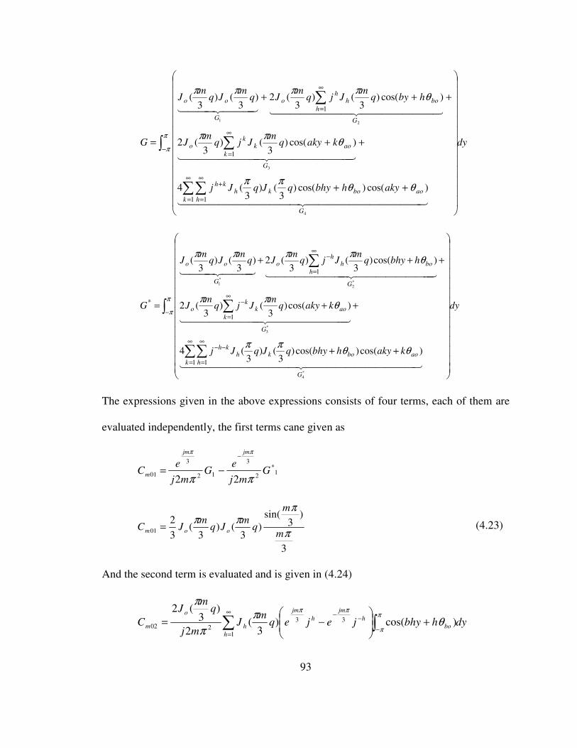
93
∫
∑∑
∑
∑
−
∞
=
∞
=
+
∞
=
∞
=
++
++
+++
=π
π
θθππ
θππ
θππππ
dy
akyhbhyqJqJj
kakyqm
Jjqm
J
hbyqm
Jjqm
Jqm
Jqm
J
G
G
ao
k
bok
h
hkh
G
ao
k
kk
o
G
bo
h
hh
o
G
oo
44444444444 344444444444 21
44444444 344444444 21
4444444 34444444 21444 3444 21
4
3
21
)cos()cos()3
()3
(4
)cos()3
()3
(2
)cos()3
()3
(2)3
()3
(
1 1
1
1
∫
∑∑
∑
∑
−
∞
=
∞
=
−−
∞
=
−
∞
=
−
++
++
+++
=π
π
θθππ
θππ
θππππ
dy
kakyhbhyqJqJj
kakyqm
Jjqm
J
hbhyqm
Jjqm
Jqm
Jqm
J
G
G
ao
k
bok
h
hkh
G
ao
k
kk
o
G
bo
h
hh
o
G
oo
44444444444 344444444444 21
44444444 344444444 21
44444444 344444444 21444 3444 21
*4
*3
*2
*1
)cos()cos()3
()3
(4
)cos()3
()3
(2
)cos()3
()3
(2)3
()3
(
1 1
1
1
*
The expressions given in the above expressions consists of four terms, each of them are
evaluated independently, the first terms cane given as
1*
2
3
12
3
0122
Gmj
eG
mj
eC
jmjm
mππ
ππ−
−=
3
)3
sin(
)3
()3
(3
201 π
πππ
m
m
qm
Jqm
JC oom = (4.23)
And the second term is evaluated and is given in (4.24)
dyhbhyjejeqm
Jmj
qm
J
C bo
h
jm
h
jm
h
h
o
m ∫∑−
−−∞
=
+
−=
π
π
ππ
θπ
π
π
)cos()3
(2
)3
(233
1202

94
Using the definition of the exponential functions
hjh
ej 2π
=
+=−=−
+−
+
−−
23sin2232333
ππππππππ
hmjeejeje
hmj
hmj
h
jm
h
jm
)cos()sin(1
23sin)
3(
)3
(2
1202 bo
hh
o
m hhbhb
hmq
mJ
m
qm
J
C θππππ
π
π
+= ∑
∞
=
(4.24)
Similarly the third terms,
)cos()sin(1
23sin)
3(
)3
(2
1203 ao
h
h
o
m kkaak
kmq
mJ
m
qm
J
C θππππ
π
π
+= ∑
∞
=
(4.25)
And finally the fourth term can be expressed as given in (4.26)
++= ∑∑
∞
=
∞
=
)(23
sin)3
()3
(4
4
1 1204 khmRqJqJ
mC
k
k
h
hm
ππππ
π (4.26)
Where
))sin(()cos(
2
1))sin((
)cos(
2
14 π
θθπ
θθba
baba
baR boaoboao −
−
−++
+
+= (4.27)
The last group consisting of the double summation determine the carrier harmonics m > 0
and n ≠ 0.
dxdyeCij
ij
M
M
nymxj
mn ∫ ∫− −
+=π
π
π
ππ)(
22
1
∫
∫
−
+−+−−
−
++
−=
π
π
θπ
θπ
π
π
π
θπ
θπ
π
π
π
dyeeemj
e
dyeeemj
eC
boao
boao
byqjm
ayqjm
jny
j
byqjm
ayqjm
jny
jm
mn
)cos(3
)cos(3
2
3
)cos(3
)cos(3
2
3
2
2
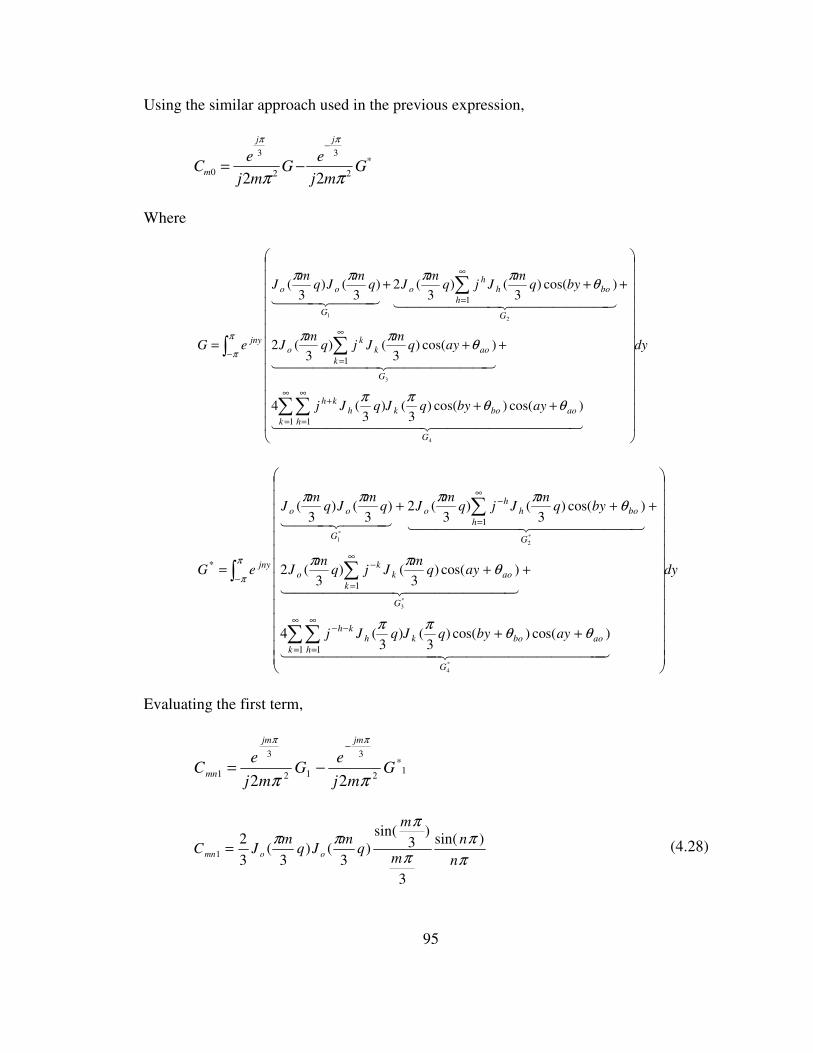
95
Using the similar approach used in the previous expression,
*
2
3
2
3
022
Gmj
eG
mj
eC
jj
mππ
ππ−
−=
Where
∫
∑∑
∑
∑
−
∞
=
∞
=
+
∞
=
∞
=
++
++
+++
=π
π
θθππ
θππ
θππππ
dy
aybyqJqJj
ayqm
Jjqm
J
byqm
Jjqm
Jqm
Jqm
J
eG
G
ao
k
bok
h
hkh
G
ao
k
kk
o
G
bo
h
hh
o
G
oo
jny
4444444444 34444444444 21
4444444 34444444 21
4444444 34444444 21444 3444 21
4
3
21
)cos()cos()3
()3
(4
)cos()3
()3
(2
)cos()3
()3
(2)3
()3
(
1 1
1
1
∫
∑∑
∑
∑
−
∞
=
∞
=
−−
∞
=
−
∞
=
−
++
++
+++
=π
π
θθππ
θππ
θππππ
dy
aybyqJqJj
ayqm
Jjqm
J
byqm
Jjqm
Jqm
Jqm
J
eG
G
ao
k
bok
h
hkh
G
ao
k
kk
o
G
bo
h
hh
o
G
oo
jny
44444444444 344444444444 21
4444444 34444444 21
4444444 34444444 21444 3444 21
*4
*3
*2
*1
)cos()cos()3
()3
(4
)cos()3
()3
(2
)cos()3
()3
(2)3
()3
(
1 1
1
1
*
Evaluating the first term,
1*
2
3
12
3
122
Gmj
eG
mj
eC
jmjm
mnππ
ππ−
−=
π
ππ
πππ
n
n
m
m
qm
Jqm
JC oomn
)sin(
3
)3
sin(
)3
()3
(3
21 = (4.28)

96
The second term becomes,
∫ ∑
∫ ∑
−
∞
=
−
−
−
∞
=
+
−+=
π
π
π
π
π
π
θππ
π
θππ
π
)cos()3
()3
(22
)cos()3
()3
(22
12
3
12
3
2
bo
h
h
h
o
jm
bo
h
h
h
o
jm
mn
byqm
Jjqm
Jmj
e
byqm
Jjqm
Jmj
eC
+= ∑
∞
= 23sin)
3(
)3
(2
2
1
2
πππ
π
πhm
Rqm
Jm
qm
J
C mn
h
h
o
mn (4.29)
Similarly,
+= ∑
∞
= 23sin)
3(
)3
(2
3
1
3
πππ
π
πkm
Rqm
Jm
qm
J
C mn
k
k
o
mn (4.30)
Where
π
π
π
π θθ
)(
))sin((
)(
))sin((3
akn
akne
akn
akneR aoao jj
mn−
−+
+
+= −
(4.31)
And the fourth term can be evaluated as follows
∫∑∑−
∞
=
∞
=
+ ++=π
πθθ
ππ
π)cos()cos()
3()
3(4
2
1
1 124 boao
jny
k
k
h
h
kh
mn byayeqJqJjmj
C
++= ∑∑
∞
=
∞
=
)(23
sin)3
()3
(4
41 1
04 khmRqJqJm
C mnk
kh
hm
ππππ
π (4.32)
Where
π
π
π
π
π
π
π
π
θθθθ
θθθθ
)(
))sin((
)(
))sin((
)(
))sin((
)(
))sin((
)()(
)()(
4
akbhn
akbhne
akbhn
akbhne
akbhn
akbhne
akbhn
akbhneR
aoboaobo
aoboaobo
jj
jj
mn
−−
−−+
+−
+−
+−+
−++
++
++=
+−−−
−+
(4.32)

97
Combining (4.28), (4.29), (4.30) and (4.32) the coefficient of the Fourier series is finally
combined as follows.
∑ ∑
∑
∑
∑∞
=
∞
−∞=
++
+
+
+
+
+
=1
4
3
2
)(23
sin)3
()3
(
23sin)
3()
3(
23sin)
3()
3(
)sin()
3sin()
3()
3(
2
m n
mnkh
mnko
mnho
oo
mn
khmRqJqJ
kmRq
mJq
mJ
hmRq
mJq
mJ
n
nmq
mJq
mJ
mC
ππππ
ππππ
ππππ
π
ππππ
π (4.33)
4.3 Input Filter Parameters Specification
A typical connection of an input filter for the matrix converter is shown in Figure 3.1.
In matrix converter with a harmonic of current-source characteristics, the second order
LC filter is preferred [57]. The current and voltage relationships of the filter are
)()()( sVsIsLR
sRLsV pii +
+= (4.34)
)()()( sIsIsVsC piif −= (4.35)
The input voltage can be expressed in terms of only the current as
[ ])()(1
)( sIsIsC
sV pi
f
i −= (4.36)
Substituting (4.36) into (4.34)
)()()(22
2
sIRsLCLRs
RsLsV
RsLCLRs
CsRCLssI p
fffff
ff
i
fffff
ffff
i++
++
++
+=

98
Figure 4.1 Schematics of input filter circuit
The input current transfer function related to input voltage is given as:
ffff
ff
i
i
CLs
CRs
Ls
Rs
sV
sI
11
11
)(
)(
2
2
++
+
= (4.37)
And the input current transfer function related to output current is
ffff
ffff
p
i
CLs
CRs
CLCRs
sI
sI
11
11
)(
)(
2 ++
+
= (4.38)
Considering the denominators of the above two transfer functions, and compare with the
second order Butterworth filter,
222 211
nn
ffff
ssCL
sCR
s ωξω ++≈++ (4.39)
Thus the characteristic frequency ωn and damping factor ξ are given as:
ff
nCL
1=ω (4.40)
ff
f
CLR2
1=ξ (4.41)

99
4.3.1 Harmonic Balance Technique
The schematic of a three phase matrix converter feeding an RL load is shown in
Figure 4.2. This typical topology is used to illustrate the design methodology proposed in
this thesis. As shown in the figure, a linear load is connected to the matrix converter
output terminal in which the output currents are considered to be pure sinusoidal and
balanced three phase. The harmonics present in the input current are totally due to the
switching. To demonstrate the dominant input current harmonics, one phase of the input
current and the corresponding three switching signals are considered for analysis.
The switching signals which generate the input phase ‘a’ current from a three phase
output current can be represented in terms of the dominant harmonics as follows.
tCtCtC
tCtCtCtCS
ycaAxcaAcaA
ycaAxcaAyaAxaAaA
)cos()cos()cos(
)cos()cos()cos()cos(3
1
765
4321
ωωωωω
ωωωωωω
+++++
−+−+++=
(4.42)
))cos((
))cos(()cos())cos(
))cos()cos()cos(3
1
7
654
321
βωω
βωωωβωω
βωωβωβω
−+
++++++−
+−−+−+++=
tC
tCtCtC
tCtCtCS
ycaB
xcaBcaBycaB
xcaByaBxaBaB
(4.43)
))cos((
))cos(()cos())cos((
))cos(()cos()cos(3
1
7
654
321
βωω
βωωωβωω
βωωβωβω
++
+−+++−−
++−+++−+=
tC
tCtCtC
tCtCtCS
ycaC
xcaCcaCycaC
xcaCyaCxaCaC
(4.44)
Where
spyspx ωωωωωω +=−=

100
Figure 4.2 A matrix converter feeding an RL load
The output three phase currents with amplitude Is and phase angle of θs are represented
as follows
))3
2cos(
))3
2cos(
)cos(
ssscs
sssbs
sssas
tII
tII
tII
θπ
ω
θπ
ω
θω
++=
+−=
+=
(4.45)
The mapping between the input and output currents of a matrix converter is shown
below.
csaCbsaBasaAap ISISISI ++= (4.46)
The input current can be obtained by substituting the switching signal expressions given
in (4.42-4.44) into (4.46). The Fast Fourier Transform (FFT) of the input current are
plotted in Figure 4.3. And it has been observed that the dominant harmonic components
of the input current are occurred at ωc- ωp and ωc+ ωp.

101
Figure 4.3 Dominant harmonics components of the input current
This input current ripple, Iapr can be given as:
+++++++
+−+++++=
tICCCCCC
tICCCCCCI
pcsaCaCaBaBaAaA
pcsaCaCaBaBaAaArippap
)cos()(2
1
)cos()(2
1
767676
434343,
ωω
ωω
(4.47)
For analysis one of the ripple components of the input current is considered which is
shown below.
tII pcprapr )cos( ωω += (4.48)
Where Ipr is the magnitude of the ripple which is given in terms of the output current and
Fourier coefficient of the switching signals.
saCaCaBaBaAaApr ICCCCCCI )(
2
1767676 +++++= (4.49)
The phase ‘a’ input current of the matrix converter consisting of a fundamental
component and a ripple part is represented as.
irpcprippap tItII θωωθω ++++= )cos()cos( (4.50)

102
Similarly, the phase ‘a’ input capacitor voltage, the filter current and source current have
the same ripple component as that of the input current.
( )vrpcprvppapr tVtVV θωωθω ++++= )(cos)cos( (4.51)
( )frpcfrfpfafr tItII θωωθω ++++= )(cos)cos( (4.52)
( )grpcgrgpgrag tItII θωωθω ++++= )(cos)cos(, (4.53)
The three phase ac source is considered to be pure sinusoidal and balanced.
3
2cos(
)3
2cos(
)cos(
πω
πω
ω
+=
−=
=
tVV
tVV
tVV
pgcg
pgbg
pgag
(4.54)
The dynamic source current shown in Figure 4.2 are given as.
cpcfcgfcggcggcg
bpbfbgfbggbggbg
apafagfaggaggag
VIIRpILIRV
VIIRpILIRV
VIIRpILIRV
+−++=
+−++=
+−++=
)(
)(
)(
(4.55)
The filter capacitor dynamics are given as
cpcgcpf
bpbgbpf
apagapf
IIpVC
IIpVC
IIpVC
−=
−=
−=
(4.56)
The three phase dynamics equation of the filter inductor are expressed as
)(
)(
)(
cfcgfcff
bfbgfbff
afagfaff
IIRpIL
IIRpIL
IIRpIL
−=
−=
−=
(4.57)

103
Since the input capacitor voltage, filter current and source current consists of a
fundamental and ripple part. Using Harmonic Balance Technique it is possible to separate
the fundamental and ripple dynamic of the input side. Before applying this technique, it is
necessary to transform input side dynamics into synchronous reference frame using the
transformation matrix given in 4.58.
+−
+−
+−
+−
=
)3
2sin()
3
2sin()sin(
)3
2cos()
3
2cos()cos(
)3
2sin()
3
2sin()sin(
)3
2cos()
3
2cos()cos(
πθ
πθθ
πθ
πθθ
πθ
πθθ
πθ
πθθ
rrr
rrr
ppp
ppp
K (4.58)
The transformed qd equation for the fundamental component of the source current
dynamics is given in (4.59). Iqg1 and Idg1 are the q-axis and d-axis components of the
fundamental component of the source current.
111111
111111
)(
)(
dpdfdgfqggpdggdggdg
qpqfqgfdggpqggqggqg
VIIRILpILIRV
VIIRILpILIRV
+−+−+=
+−+++=
ω
ω (4.59)
The dynamics equations for the fundamental q-axis and d-axis filter current, Iqf1 and Idf1
are given as
)(
)(
1111
1111
dfdgfqffpdff
qfqgfdffpqff
IIRILpIL
IIRILpIL
−=−
−=+
ω
ω (4.60)
Similarly, the input capacitor voltage
1111
1111
dpdgqpfpdpf
qpqgdpfpqpf
IIVCpVC
IIVCpVC
−=−
−=+
ω
ω (4.61)

104
Similarly, the ripple dynamic equations for the source current are given below where Iqgr
and Idgr are the q-axis and d-axis ripple components of the source current. Iqfr and Idfr are
the corresponding filter current ripples. Similarly, Vqpr and Vdpr stand for the ripple axes
components of the input capacitor voltages.
dprdfrdgrfqggpcdgrgdgrg
qprqfrqgrfdgrgpcqgrgqgrg
VIIRILpILIR
VIIRILpILIR
+−++−+=
+−++++=
)()(0
)()(0
1ωω
ωω (4.62)
The ripple dynamics for the filter current in synchronous reference frame are expressed in
(4.63).
)()(
)()(
dfrdgrfqfrfpcdfrf
qfrqgrfdfrfpcqfrf
IIRILpIL
IIRILpIL
−=+−
−=++
ωω
ωω (4.63)
Similarly, the input capacitor voltage dynamics are given as
dprdgrqprfpcdprf
qprqgrdprfpcqprf
IIVCpVC
IIVCpVC
−=+−
−=++
)(
)(
ωω
ωω (4.64)
At steady state where the time derivatives, p = 0 the expression given from (4.62) to
(4.64) becomes,
dprdfrfqgrgpcdgrfg
qprqfrfdgrgpcqgrfg
VIRILIRR
VIRILIRR
+−+−+=
+−+++=
)()(0
)()(0
ωω
ωω (4.65)
)()(
)()(
dfrdgrfqfrfpc
qfrqgrfdfrfpc
IIRIL
IIRIL
−=+−
−=+
ωω
ωω (4.66)
dprdgrqprfpc
qprqgrdprfpc
IIVC
IIVC
−=+−
−=+
)(
)(
ωω
ωω (4.67)

105
From (4.66), the q-axis and d-axis filter current can be expressed in terms of the source
currents as follow.
dgr
fpcf
ffpc
qgr
fpcf
f
qfr ILR
RLI
LR
RI
222222
2
)(
)(
)( ωω
ωω
ωω ++
+−
++= (4.68)
dgr
fpcf
f
qgr
fpcf
ffpc
dfr ILR
RI
LR
RLI
222
2
222 )()(
)(
ωωωω
ωω
+++
++
+= (4.69)
Since the input current ripple component is a function of the output current and the
Fourier coefficient, (4.67) can be modified as given (4.70). Kripp is a coefficient computed
from the coefficients of the switching signal components which result in the particular
input current ripple.
qsrippqgrdprfpc IKIVC −=+ )( ωω (4.70)
dsrippdgrqprfpc IKIVC −=+− )( ωω (4.71)
Substituting (4.68) and (4.69) into (4.65),
qprdgr
fpcf
ffpc
gpcqgr
fpcf
f
fg VILR
RLLI
LR
RRR +
++
++++
++−+=
222
2
222
3
)(
)()(
)(0
ωω
ωωωω
ωω (4.72)
dprqgr
fpcf
ffpc
gpcdgr
fpcf
f
fg VILR
RLLI
LR
RRR +
++
+++−
++−+=
222
2
222
3
)(
)()(
)(0
ωω
ωωωω
ωω (4.73)
Since the filter parameters are selected based on the specified maximum allowable source
current and input capacitor voltage ripples, Igr and Vpr.
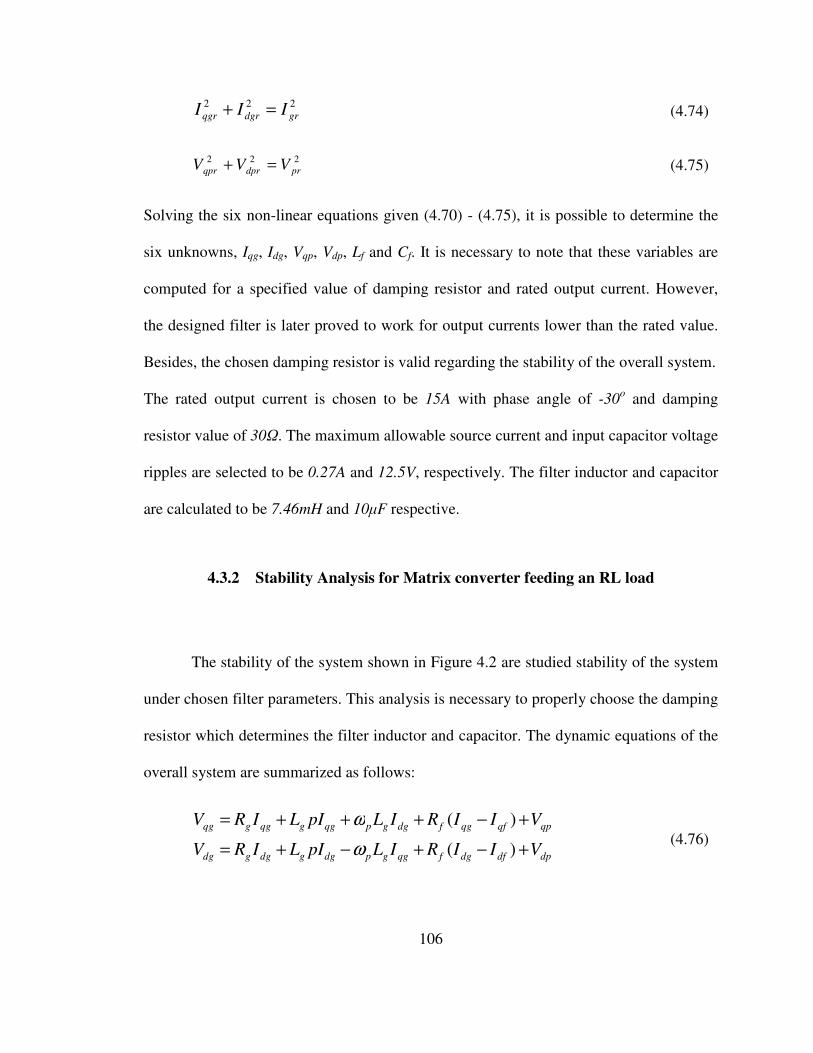
106
222
grdgrqgr III =+ (4.74)
222
prdprqpr VVV =+ (4.75)
Solving the six non-linear equations given (4.70) - (4.75), it is possible to determine the
six unknowns, Iqg, Idg, Vqp, Vdp, Lf and Cf. It is necessary to note that these variables are
computed for a specified value of damping resistor and rated output current. However,
the designed filter is later proved to work for output currents lower than the rated value.
Besides, the chosen damping resistor is valid regarding the stability of the overall system.
The rated output current is chosen to be 15A with phase angle of -30o and damping
resistor value of 30Ω. The maximum allowable source current and input capacitor voltage
ripples are selected to be 0.27A and 12.5V, respectively. The filter inductor and capacitor
are calculated to be 7.46mH and 10µF respective.
4.3.2 Stability Analysis for Matrix converter feeding an RL load
The stability of the system shown in Figure 4.2 are studied stability of the system
under chosen filter parameters. This analysis is necessary to properly choose the damping
resistor which determines the filter inductor and capacitor. The dynamic equations of the
overall system are summarized as follows:
dpdfdgfqggpdggdggdg
qpqfqgfdggpqggqggqg
VIIRILpILIRV
VIIRILpILIRV
+−+−+=
+−+++=
)(
)(
ω
ω (4.76)

107
)(
)(
dfdgfqfgpqff
qfqgfdfgpqff
IIRILpIL
IIRILpIL
−=−
−=+
ω
ω (4.77)
dpdgqpfpdpf
qpqgdpfpqpf
IIVCpVC
IIVCpVC
−=−
−=+
ω
ω (4.78)
The dynamics of digital filter in synchronous reference frame are
)(1
)(1
dfdpdf
qfqpqf
VVpV
VVpV
−=
−=
τ
τ (4.79)
The output current dynamics are given in qd reference frame as given below where Vqs
and Vds are the output voltages where as Iqs and Ids are the output current axes
components.
qssdssdssds
dssqssqssqs
IpILIRV
IpILIRV
ω
ω
−+=
++= (4.80)
The mapping between the input and output of the matrix converter current and voltage
relations are given as
dsdqqsqqqp
dsddqsqddp
IMIMI
IMIMI
+=
+= (4.81)
The modulation signal components, Mqq, Mqd, Mdq and Mdd are discussed in detail in the
subsequent chapters. The output voltage is also written in terms of the input capacitor
voltage as follow.
dpddqpdqds
dpqdqpqqqs
VMVMV
VMVMV
+=
+= (4.82)

108
The stability study involves the small signal modeling and steady state analysis for
system shown in the Figure 4.2. The linearization of the system dynamics around steady
state operating point leads to the following small signal model of the system.
( )qpdggpqffqgfgqg
g
qg VILIRIRRVL
Ip ∆−∆−∆+∆+−∆=∆ ω)(1
( )dpqggpdffdgfgdg
g
dg VILIRIRRVL
Ip ∆−∆+∆+∆+−∆=∆ ω)(1
( )dffpqffqgf
f
qf ILIRIRL
Ip ∆−∆−∆=∆ ω1
( )dffpqffqgf
f
qf ILIRIRL
Ip ∆−∆−∆=∆ ω1
( )dffpqffqgf
f
qf ILIRIRL
Ip ∆−∆−∆=∆ ω1
( )dqdsoqqqsodsdqoqsqqodpfpqg
f
qp MIMIIMIMVCIC
Vp ∆−∆−∆−∆−∆−∆=∆ ω1
( )dddsoqdqsodsddoqsqdoqpfpdg
f
dp MIMIIMIMVCIC
Vp ∆−∆−∆−∆−+∆=∆ ω1
)(1
qfqpqf VVVp ∆−∆=∆τ
)(1
dfdpdf VVVp ∆−∆=∆τ
( )qddpoqqqpodsssqssdpqdoqpqqo
o
qs MVMVILIRVMVML
Ip ∆+∆+∆−∆−∆+∆=∆ ω1
( )dddpodqqpoqsssdssdpddoqpdqo
s
ds MVMVILIRVMVML
Ip ∆+∆+∆+∆−∆+∆=∆ ω1

109
The characteristic matrix is shown (4.83) and it depends on the operating points.
−−−
−−−−
−
−
−
−
−−
−+
−
−−+
−
=
s
ss
s
s
s
p
f
p
f
f
f
p
f
f
p
f
f
f
f
gg
f
g
fg
p
gg
f
p
g
fg
L
Rxxxx
L
Rxxxx
zzyyC
zzyyC
L
R
L
R
L
R
L
R
LL
R
L
RR
LL
R
L
RR
A
ω
ω
ττ
ττ
ω
ω
ω
ω
ω
ω
4343
2121
3343
2121
0000
0000
001
01
00000
0001
01
0000
0001
0
00001
0000000
0000000
00001
00
000001
0
(4.83)
The constants represented in the matrix are computed at the steady state operation.
21
po
qpoqso
V
VVx −=
22
po
dpoqso
V
VVx −=
23
po
qpodso
V
VVx −=
24
po
dpodso
V
VVx −=
4
22
41
)(1
po
dpoqpo
f V
kVV
Cyy
−=−=
432
21
po
dpoqpo
f V
kVV
Cyy ==
dsodsoqsoqso IVIVk +=

110
Table 4.1 System parameters
Vs = 160V fs = 50Hz
Rs = 10Ω Ls =20mH for Is = 15A with -30o
Rs = 30Ω Ls =60mH for Is = 5A with -30o
Vg = 230V fp = 60Hz Rg = 0.5Ω, Lg = 1mH
Rf = 30Ω Lf = 7.46mH Cf = 10µF
The steady state variables are computed step-by-step as follows for the given parameter
For varies damping resistance the operating points are computed to analyze the Eigen
value of the characteristic matrix given above. The operating points by solving the
quadratic equation shown in (4.84)
02 =++ cbMaM dddd (4.82)
ddxdq MggMM 21−=
ds
qsddqd
V
VMM =
qd
dd
dqqq M
M
MM =
)(11 dsddqsqdqgqp IMIMgVkV ++=
)(43 qpqgqg VVI −= ββ
qgdg II ρ=
)(4 qpqgdp VVV −= β
qgqf II 1β=
qgdf II 2β=

111
4.4 Simulation Results and Discussion
Using the system parameter given in Table 4.1 which is based on the designed filter,
simulations are done to examine the effect of the damping resistor on the system stability
as well as to verify the filter designed based on the proposed method in mitigating the
harmonic in the input current. Figure 4.4 show the stability limit of the studied system in
terms of the voltage transfer ratio and digital filter time constant. It is observed that
higher filter time constant results in wider range of stability region. The figure also shows
that to operate in higher voltage gain, the corresponding digital filter should have higher
time constant to keep the overall system stable. The effect of the damping resistance on
the system stability is shown in Figure 4.5 by analyzing the dominant Eigen value for
each value of damping resistances. Note that this dominant Eigen value varies with the
damping resistance and therefore it is necessary to particularly selected dominant Eigen
value as the resistance vary. It is seen that with the select damping resistance, Rf = 30Ω,
the system is stable even in lower digital time constant. It can also be observed from the
figure that, lower resistance leads to a better system stability; however, the low value of
damping resistance will lead to higher power loss in the filter.
Simulations are also done to observe the resulting input and output waveforms of
the matrix converter –RL load system. A sinusoidal input voltage with input unity power
factor is considered for simulation as shown in Figure 4.6. As seen in the Figure 4.7, the
designed input filter maintained sufficiently high power factor at the input terminal of the
converter which allows wide range of output voltage operation.

112
Figure 4.4 Stability limit of a matrix converter with RL load
Figure 4.5 Dominant Eigen Values for various damping resistance
Voltage t
ransfe
r ra
tio,
q
τ [ms]
0.05 0.1 0.15 0.2 0.25 0.3 0.35 0.40.3
0.4
0.5
0.6
0.7
0.8Unstable region
Stable region
10 20 30 40 50 60 70 80 90 100-1200
-1000
-800
-600
-400
-200
0
200
400
600
800
Damping Resistance, Rf [Ω ]
Dom
inant
Eig
en V
alu
e
τ=0.1ms
τ=0.2ms
τ=0.3ms

113
Figure 4.6 Phase ‘a’ source voltage and current
Figure 4.7 Phase ‘a’ input capacitor voltage and current of the MC
The source current shown in figure above are magnified by twenty times. The averaged
output voltage and current with 10 times magnified are shown in Figure 4.8. The input
current of the converter before and source current which is after the filter is shown in
Figure 4.9.
0.1 0.105 0.11 0.115 0.12 0.125 0.13 0.135 0.14 0.145 0.15
-300
-200
-100
0
100
200
300
Time [sec]
Vag
[V]Iag
[V]
0.1 0.105 0.11 0.115 0.12 0.125 0.13 0.135 0.14 0.145 0.15
-300
-200
-100
0
100
200
300
Time [sec]
Vap
[V] Iap
[A]
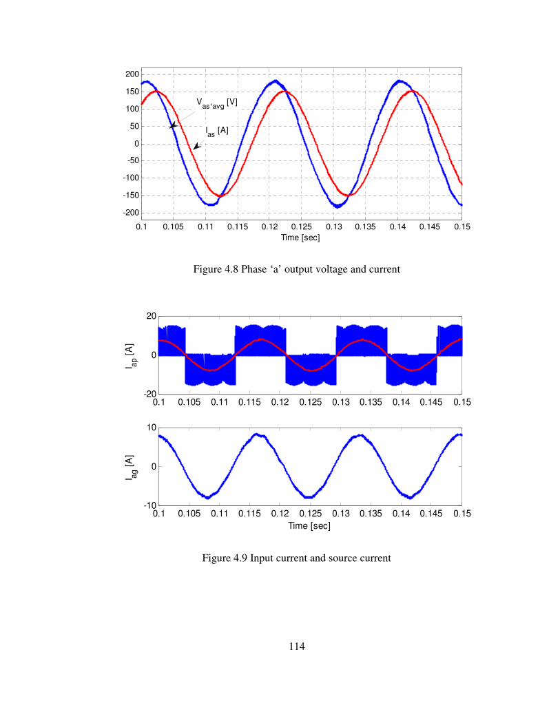
114
Figure 4.8 Phase ‘a’ output voltage and current
Figure 4.9 Input current and source current
0.1 0.105 0.11 0.115 0.12 0.125 0.13 0.135 0.14 0.145 0.15
-200
-150
-100
-50
0
50
100
150
200
Time [sec]
Ias
[A]
Vas
,avg
[V]
0.1 0.105 0.11 0.115 0.12 0.125 0.13 0.135 0.14 0.145 0.15-20
0
20
I ap [
A]
0.1 0.105 0.11 0.115 0.12 0.125 0.13 0.135 0.14 0.145 0.15-10
0
10
I ag [
A]
Time [sec]

115
Figure 4.10 FFT of input current of the MC
Figure 4.11 FFT of the source current
The harmonic content of Figure 4.9 are presented in the above two figures. The
dominant harmonic of the input current is as high as 4A and the next dominant harmonics
is around 3.4A. As observed in Figure 4.11, these harmonics are greatly reduced in the
source current due to the input filter. From this result it can be concluded that even if the
proposed filter parameter considered only one of the dominant harmonics, it also
mitigates the other harmonics.

116
Figure 4.12 FFT of the input capacitor voltage
Figure 4.12 shows the harmonic component of the input capacitor voltage. With the
designed input filter, the input capacitor voltage and source current ripples meet the
specified maximum allowable ripples as demonstrated in Figure 4.11 and Figure 4.12.
The stability of the system under the determined filter capacitor and inductor
values for an output current of 5A is studied. As observed in Figure 4.13, the damping
resistance does not affect the system stability under low output current. And therefore,
the filter designed based on output rated current can also work for lower current
operation.
The Bode plot of the filter transfer function given in (4.38) is shown in Figure
4.14. This figure shows that the gain at the resonance frequency, 583Hz is near to zero
and therefore, it can be concluded that the chosen filter parameters can also result in very
less oscillation at the characteristic frequency.

117
Figure 4.13 Stability limit for a load current of 5A
Figure 4.14 Bode plot of the designed input filter
10 20 30 40 50 60 70 80 90 100-2500
-2000
-1500
-1000
-500
0
Damping Resistance, Rf [Ω ]
Dom
inant
Eig
en V
alu
e
τ=0.1ms
τ=0.2ms
τ=0.3ms
-30
-20
-10
0
10
Magnitu
de (
dB
)
102
103
104
105
-135
-90
-45
0
Phase (
deg)
Frequency (rad/sec)

118
4.5 Conclusion
This chapter propose a new input filter design for a matrix converter which mitigate
unwanted harmonic generated by the high frequency switching. A harmonic balance
technique is set forth which enables an independent analysis for the ripple component of
the current and voltage waveform. The filter inductor and capacitor are determined based
on the specified maximum allowable source current and input capacitor voltage ripples
under a given damping resistance and output rated current. Stability of the overall system
is studied with the help of small signal modelling and steady state analysis. Simulation
results shows that the system is stable under the chosen damping resistor even with a low
digital low pass filter’s time constant. Moreover, the designed filter parameters which are
determined based on the rated output current perfectly works lower output currents.
Although the analysis is consider only one dominant harmonic component of the input
current, the resulting filter are capable of mitigating lower harmonics as well. It is also
observed that the proposed approach maintained a high power factor at the input terminal
of the matrix converter which allows wider control range of a matrix converter. Based on
the transfer function of the filter, the chosen damping resistance is sufficiently damp the
oscillation near the resonant frequency and besides this resonance frequency is far from
the fundamental and sufficiently lower that the switching frequency. Finally, this new
approach can be implemented when the source voltage contained harmonics although this
work assumes a pure ac source.

119
CHAPTER 5
DYANMIC AND STEADY STATE MODELLING OF MATRIX
CONVERTER SYSTEMS
5.1 Introduction
This chapter presents the complete modelling of a matrix converter feeding a
passive RL load. It also gives a detailed steady state analysis supported by a computer
simulation. The model implements the carrier based modulation strategies developed in
the chapter 3. The dynamic and steady state performance analysis of a matrix converter
fed induction motor are presented in this chapter. A new generalized stead state analysis
which can be implemented for matrix converter based drives operating in both unity and
non unity input factor operations. The motivation behind this analysis is that most of the
literature gives a steady state operating points computed under unity input power factor
operation. With the help of this generalized analysis, it is possible to study the
performance of the drive under lagging, unity or leading input power factor. Moreover,
this analysis is used to evaluate the operating points for the stability study of the drive
system. Computer simulations results obtained using a MATLAB/Simulink platform
have been provided to verify the starting transient, dynamic response and the steady state
performance of the drive.

120
5.2 Matrix Converter Feeding an RL Load
5.2.1 Dynamic Modelling
The topology of the overall system which comprises a three phase power supply, an
input LC filter, digital low pass filter, modulation signal and switching signal generation
blocks and three phase-to-phase AC/AC matrix converter feeding a passive load is
schematically shown in Figure 5.1. The digital low pass filter is implemented in
synchronous reference frame; therefore, the measured input capacitor voltages first
transformed to qd synchronous reference frame and then transformed back to abc after
the low pass filter. These filtered capacitor voltages are then used to determine the
appropriate modulation signals which are compared with high frequency triangular
carrier signal to generate the actual switching pulses. The modulation scheme used
throughout the modelling is carrier-based PWM or duty-cycle technique.
Complying with the Kirchhoff’s voltage and current laws, the switching functions
are constrained as follows.
1
1
1
=++
=++
=++
cCbCaC
cBbBaB
cAbAaA
SSS
SSS
SSS
(5.1)
The three phase voltage equations for the input side of the MC are given in (5.2)
assuming the common mode voltage between point p and o shown in Figure 5.1 are zero.
The term p represents the time derivatives (d/dt).

121
Figure 5.1 Schematic diagram of AC/AC matrix converter feeding an RL load
The dynamic equations for the filter capacitor voltages are expressed in (5.4). Where Iag,
Ibg and Icg are the three phase source current while Iap, Ibp and Icp are the three phase input
current of the matrix converter. Vap, Vbp and Vcp represent the input three phase capacitor
voltages.
cpcgcpf
bpbgbpf
apagapf
IIpVC
IIpVC
IIpVC
−=
−=
−=
(5.4)
The mapping of the input phase voltages and output phase voltages of the converter are
related as in (5.5). Vas, Vbs and Vcs are the output three phase voltages.

122
cpcCbpbCapaCnpcs
cpcBbpbBapaBnpbs
cpcAbpbAapaAnpas
VSVSVSVV
VSVSVSVV
VSVSVSVV
++=+
++=+
++=+
(5.5)
For a balanced output voltage, the sum of the output phase voltages becomes zero.
Summing all the rows in (5.5), the expression for Vnp is given by (5.6).
++++
++++=
bpcCbpbCapaCbpcBbpbB
apaBbpcAbpbAapaA
npVSVSVSVSVS
VSVSVSVSV
3
1 (5.6)
The input and output phase currents are related by switching function given by (5.7)
where Ias, Ibs and Ics are the output currents.
cscCbscBascAcp
csbCbsbBasbAbp
csaCbsaBasaAap
ISISISI
ISISISI
ISISISI
++=
++=
++=
(5.7)
The output RL load voltage equations are expressed in (5.8) where Rs and Ls are
respectively the resistance and inductance of the passive load.
csscsscs
bssbssbs
assassas
pILIRV
pILIRV
pILIRV
+=
+=
+=
(5.8)
The expression for the digital low pass filter is given in the synchronous reference frame
since it does not introduce any phase angle and attenuation on the fundamental
component of the input voltage [40]. Vqf and Vdf are the q-axis and d-axis of the filtered
capacitor voltages and τ represents the time constant of the digital low pass filter.
)(1
)(1
dfdpdf
qfqpqf
VVpV
VVpV
−=
−=
τ
τ (5.9)
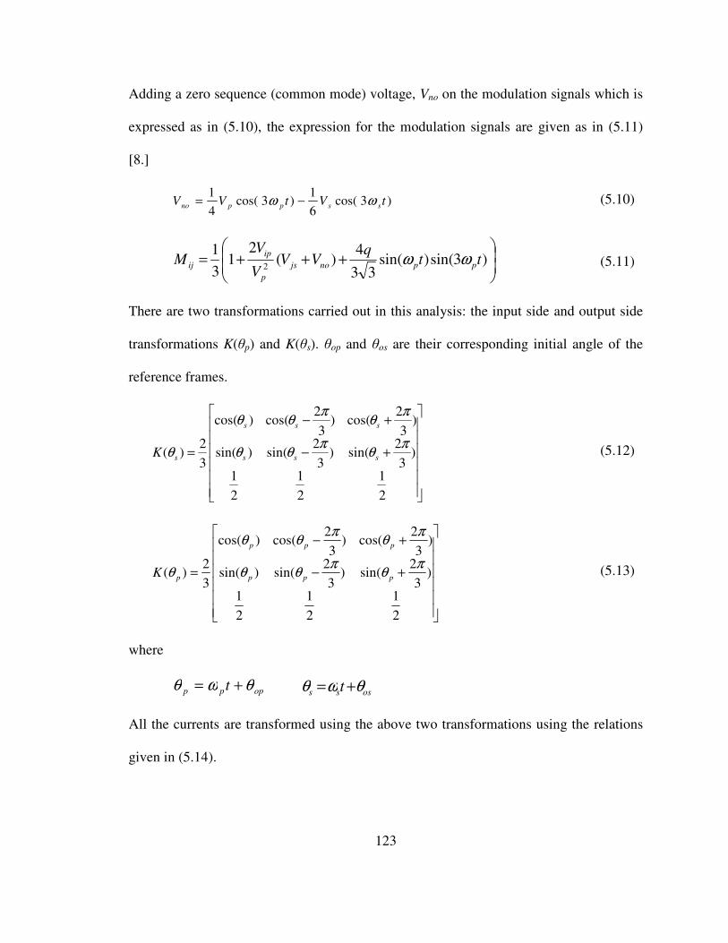
123
Adding a zero sequence (common mode) voltage, Vno on the modulation signals which is
expressed as in (5.10), the expression for the modulation signals are given as in (5.11)
[8.]
)3cos(6
1)3cos(
4
1tVtVV ssppno ωω −= (5.10)
+++= )3sin()sin(
33
4)(
21
3
12
ttq
VVV
VM ppnojs
p
ip
ij ωω (5.11)
There are two transformations carried out in this analysis: the input side and output side
transformations K(θp) and K(θs). θop and θos are their corresponding initial angle of the
reference frames.
+−
+−
=
2
1
2
1
2
1
)3
2sin()
3
2sin()sin(
)3
2cos()
3
2cos()cos(
3
2)(
πθ
πθθ
πθ
πθθ
θ sss
sss
sK (5.12)
+−
+−
=
2
1
2
1
2
1
)3
2sin()
3
2sin()sin(
)3
2cos()
3
2cos()cos(
3
2)(
πθ
πθθ
πθ
πθθ
θ ppp
ppp
pK (5.13)
where
oppp t θωθ += osss t θωθ +=
All the currents are transformed using the above two transformations using the relations
given in (5.14).

124
abcssqds
abcss
T
pqdp
abcfpqdf
abcgpqdg
IKI
IKSKI
IKI
IKI
)(
)()(
)(
)(
1
θ
θθ
θ
θ
=
=
=
=
− (5.14)
Iaf, Ibf and Icf are the three phase current flowing through the filter inductor. Note that the
currents shown below are a vector of three elements
=
og
dg
qg
qdg
I
I
I
I
=
of
df
qf
qdf
I
I
I
I
=
op
dp
qp
qdp
I
I
I
I
=
os
ds
qs
qds
I
I
I
I
where
Iqg- the q-axis source current
Idg - the d-axis source current
Iqf - the q-axis filter current
Idg - the d-axis source current
Iqp - the q-axis input current of the matrix converter
Idp- the d-axis input current of the matrix converter
Iqs- the q-axis output current
Iqs - the d-axis output current
=
cg
bg
ag
abcg
I
I
I
I
=
cf
bf
af
abcf
I
I
I
I
=
cp
bp
ap
abcp
I
I
I
I
=
cs
bs
as
abcs
I
I
I
I

125
Similarly, the voltages are transformed to synchronous qd axis as follows.
abcppsqds
abcppqdp
abcgpqdg
VSKKV
VKV
VKV
)()(
)(
)(
1 θθ
θ
θ
−=
=
=
(5.15)
where
=
og
dg
qg
qdg
V
V
V
V
=
op
dp
qp
qdp
V
V
V
V
=
os
ds
qs
qds
V
V
V
V
And
Vqg ,Vdg - the q-axis and d-axis source voltages
Vqp, Vdp - the q-axis and d-axis input capacitor voltages
Vqs, Vds - the q-axis and d-axis output voltages
=
cg
bg
ag
qdg
V
V
V
V
=
p
bp
ap
qdp
V
V
V
V
=
cs
bs
as
qds
V
V
V
V
Using (5.14) and (5.15) the synchronous reference frame source voltage expression is
given as
dpdfdgfqggpdggdggdg
qpqfqgfdggpqggqggqg
VIIRILpILIRV
VIIRILpILIRV
+−+−+=
+−+++=
)(
)(
ω
ω (5.16)
The qd axis voltage is expressed as
)(
)(
dfdgfqfgpqff
qfqgfdfgpqff
IIRILpIL
IIRILpIL
−=−
−=+
ω
ω (5.17)

126
Similarly, the capacitor dynamics in qd is shown below
dpdgqpfpdpf
qpqgdpfpqpf
IIVCpVC
IIVCpVC
−=−
−=+
ω
ω (5.18)
The mapping between the input and output current is done using the four components of
a modulation signals. The detailed derivation for the expression given in (5.19-5.23) is
given in Appendix E.
dsdqqsqqqp
dsddqsqddp
IMIMI
IMIMI
+=
+= (5.19)
The expressions of the synchronous frame modulation signals are shown as follows,
)sin()sin()cos()sin(
)sin()cos()cos()cos(
ppssddppssdq
ppssqdppssqq
MMMM
MMMM
δδδδ
δδδδ
=−=
−== (5.20)
where δop and δos are the phase angle of the capacitor and output voltages respectively.
opopppososss θδδθδδ −=−= (5.21)
The modulation index of the matrix converter is related to each component of the
modulation signals as follows
22222
dddqqdqq MMMMM +++= (5.22)
The input output voltage mapping in qd is represented in (5.23)
dpddqpdqds
dpqdqpqqqs
VMVMV
VMVMV
+=
+= (5.23)
Finally, the output voltage of the converter given
qssdssdssds
dssqssqssqs
IpILIRV
IpILIRV
ω
ω
−+=
++= (5.24)

127
Figure 5.2 Switching pulses for phase ‘a’ output voltage
5.2.2 Dynamic Simulation Results and Discussion
Based on the model equation derived in the previous section and with the
parameters given in Table 5.1, simulations are given in Figure 5.2 to 5.8. The switching
signals used to synthesize output phase ‘a’ voltage are shown in Figure 5.2 where at any
instant of time one and only one device turns ON. The output line-to-line voltages are
given in Figure 5.3 with an average sinusoidal waveform. Similarly, the three phase
voltages are all sinusoidal average voltages and balanced as seen in Figure 5.5. The input
phase capacitor voltage containing small ripple are shown in Figure 5.5 and are filtered
by the digital low pass filter before they are used to generate a modulation signals.
0.4 0.4005 0.401 0.4015 0.402 0.4025 0.403 0.4035 0.404 0.4045 0.405
0
0.5
1
SaA
0.3 0.3005 0.301 0.3015 0.302 0.3025 0.303 0.3035 0.304 0.3045 0.305
0
0.5
1
SbA
0.3 0.3005 0.301 0.3015 0.302 0.3025 0.303 0.3035 0.304 0.3045 0.305
0
0.5
1
ScA
Time [Sec]

128
Figure 5.3 MC output line-to-line voltages
Figure 5.4 MC output three phase voltages
`
0.1 0.11 0.12 0.13 0.14 0.15 0.16
-500
0
500
Vab [
V]
0.1 0.11 0.12 0.13 0.14 0.15 0.16
-500
0
500V
bc [
V]
0.1 0.11 0.12 0.13 0.14 0.15 0.16
-500
0
500
Vca [
V]
Time [sec]
0.1 0.11 0.12 0.13 0.14 0.15 0.16-400
-200
0
200
400
Vas [
V]
0.1 0.11 0.12 0.13 0.14 0.15 0.16-400
-200
0
200
400
Vbs [
V]
0.1 0.11 0.12 0.13 0.14 0.15 0.16-400
-200
0
200
400
Vcs [
V]
Time [sec]

129
Figure 5.5 Input three phase capacitor voltages
Figure 5.6 Filtered three phase capacitor voltages
0.1 0.105 0.11 0.115 0.12 0.125 0.13 0.135 0.14 0.145 0.15
-200
0
200
Vap [
V]
0.1 0.105 0.11 0.115 0.12 0.125 0.13 0.135 0.14 0.145 0.15
-200
0
200V
bp [
V]
0.1 0.105 0.11 0.115 0.12 0.125 0.13 0.135 0.14 0.145 0.15
-200
0
200
Vcp [
V]
Time [sec]
0.1 0.105 0.11 0.115 0.12 0.125 0.13 0.135 0.14 0.145 0.15
-200
0
200
Vaf [
V]
0.1 0.105 0.11 0.115 0.12 0.125 0.13 0.135 0.14 0.145 0.15
-200
0
200
Vbf [
V]
0.1 0.105 0.11 0.115 0.12 0.125 0.13 0.135 0.14 0.145 0.15
-200
0
200
Vcf [
V]
Time [sec]

130
Figure 5.7 MC three phase input current
Figure 5.8 Three phase source currents
0.1 0.105 0.11 0.115 0.12 0.125 0.13 0.135 0.14 0.145 0.15
-10
0
10
I ap [
A]
0.1 0.105 0.11 0.115 0.12 0.125 0.13 0.135 0.14 0.145 0.15
-10
0
10I b
p [
A]
0.1 0.105 0.11 0.115 0.12 0.125 0.13 0.135 0.14 0.145 0.15
-10
0
10
I cp [
A]
Time [sec]
0.1 0.105 0.11 0.115 0.12 0.125 0.13 0.135 0.14 0.145 0.15-10
0
10
I ag [A
]
0.1 0.105 0.11 0.115 0.12 0.125 0.13 0.135 0.14 0.145 0.15-10
0
10
I bg [A
]
0.1 0.105 0.11 0.115 0.12 0.125 0.13 0.135 0.14 0.145 0.15-10
0
10
I cg [A
]
Time [sec]

131
These filtered input voltages are given in Figure 5.6. The input current of the
matrix converter and the source current after the input low pass filter is show in Figure
5.7 and 5.8 respectively.
5.2.3 Generalized Steady State Analysis
The generalized steady state analysis proposed in this thesis is presented in this
section. To determine the steady state analysis, the dynamic equations given in abc are
transformed into qd synchronous reference frames. At steady state the q-axis and d-axis
voltage equations of the source are expressed as
dpdfdgfqggpdggdg
qpqfqgfdggpqggqg
VIIRILIRV
VIIRILIRV
+−+−=
+−++=
)(
)(
ω
ω (5.25)
The voltage equations for the inductor voltage at steady state are
)(
)(
dfdgfqffp
qfqgfdffp
IIRIL
IIRIL
−=−
−=
ω
ω (5.26)
The q-axis and d-axis voltage equations for the inductor voltage at steady state is given as
dsddqsqddgqpfp
dsdqqsqqqgdpfp
IMIMIVC
IMIMIVC
−−=−
−−=
ω
ω (5.27)
The active and reactive power drawn from the source can be represented in terms of the
synchronous reference frame voltages and currents as follows:

132
)(2
3
)(2
3
qgdgdgqgg
dgdgqgqgg
IVIVQ
IVIVP
−=
+=
(5.28)
Aligning the input side reference frame angle to the d-axis of the source voltage, the d-
axis of the source voltage becomes zero and the q-axis source voltage is equal to the
magnitude of the phase voltage. The expressions for the active and reactive power are
modified as shown in (5.29).
dgggqggg IVQIVP2
3
2
3== (5.29)
Considering the output sides, the steady state synchronous reference frame voltage
equations are
qsssdssds
dsssqssqs
ILIRV
ILIRV
ω
ω
−=
+= (5.30)
The corresponding q-axis and d-axis load current can be computed from the respective
voltages using expression (5.31)
ds
sss
sqs
sss
ssds
ds
sss
ssqs
sss
sqs
VLR
RV
LR
LI
VLR
LV
LR
RI
222222
222222
ωω
ω
ω
ω
ω
++
+=
+−
+=
(5.31)
Since this particular approaches is a generalized method of steady state analysis, it can be
used when the whole system operate a unity, lagging or leading power factor at the
source side. By specifying the operating input power factor (pf), based on (5.29) the

133
relation between the q-axis and d-axis components of the source current can easily
represented as shown below.
qgdg II ρ= (5.32)
where ρ is the ratio of the reactive power to the active power
The qd components of the inductor current can also be represented in terms of the q-axis
source current by simultaneously solving (5.26).
qgdf
qgqf
II
II
2
1
β
β
=
= (5.33)
The constants which are function of the input frequency, input power factor, filter
inductor and damping resistor are represented below.
f
fpf
fpf
f
fpf
fpf
RLR
LR
RLR
LR
2222
2221
ω
ωρβ
ω
ρωβ
+
+=
+
−=
(5.34)
Substituting (5.33) into (5.25), all the input side voltages and currents can be represented
in terms of only the q-axis capacitor voltage which is represented by (5.35)
)(
)(
4
43
qpqgdp
qpqgqg
VVV
VVI
−=
−=
β
ββ (5.35)
where the expressions of the above constants are given in (5.36) and it is seen that all
these constants so far does not depend on the filter capacitor parameter.

134
))1((
1
))((
1
13
4
2
3
gpfg
fgfgp
LRR
RRRL
ρωβββ
ρβωβ
+−+=
+−+=
(5.36)
The input and output voltage now are related by the four components of the modulation
signals.
dpddqpdqds
dpqdqpqqqs
VMVMV
VMVMV
+=
+=
(5.37)
Similarly, the input current components are related to the output voltages by these
modulation signal components.
dsddqsqddp
dsdqqsqqqp
IMIMI
IMIMI
+=
+= (5.38)
These four components of the modulation signals are represented in (5.39) where M is the
modulation index, δss is the phase angle difference between the output voltage and output
side reference frame. And δpp is the phase angle difference between the input capacitor
voltage and input side reference frame. The complete derivation is given in Appendix IV.
22222
)sin()sin(
)cos()sin(
)sin()cos(
)cos()cos(
dddqqdqq
ppssdd
ppssdq
ppssqd
ppssqq
MMMMM
MM
MM
MM
MM
+++=
=
−=
−=
=
δδ
δδ
δδ
δδ
` (5.39)
Defining constants k1 and g1 as given in (5.40), Vqp can be represented in terms of the
other variables.

135
fp
fp
Cg
Ck
ωβρβ
ωβρβ
βρβ
−−=
−=
43
1
43
43
1
1 (5.40)
)(11 dsddqsqdqgqp IMIMgVkV ++= (5.41)
The four non-linear equation and four variables, Mqq, Mqd, Mdq and Mdd, are shown in
(5.42). Eliminating three of the four unknowns, first Mqq then Mdq and later Mqd , makes
the computation easier and it does not need mathematical tools.
( )( )
( ) dsdqqsqqqgdsddqsqdqg
qgdddsddqsqdqgdddqds
qgqddsddqsqdqgqdqqqs
dqqdddqq
IMIMVgIMIMgVkg
VMIMIMgVkMMV
VMIMIMgVkMMV
MMMM
−−=++
+++−=
+++−=
=
2112
4114
4114
)(
)()(
)()(
ββ
ββ
(5.42)
The final quadratic equation which is a function of Mdd is shown (5.43). Once Mdd is
computed all the other variables are determined by back substitution.
02 =++ cbMaM dddd (5.43)
The coefficients of the quadratic equations are given as follows.
dsdsqsqs
dsqg
x
fp
qgdsxds
dsqg
dsdsqsqs
IVIV
kVVgM
Cg
VVMkVc
VVggggkggkb
IVIVggga
+
−=
−=
−=
+−++=
++=
)1(
))()((
)))((
12
4432
1
2
2142114211
4211
βωββ
ββ
β
(5.46)

136
5.2.4 Steady State Simulation Results and Discussions
In order to verify the analysis, simulation of a MC system with the parameters
given in Table 5.1 is performed. Figure 5.9 to Figure 5.13 shows the steady state
simulation results of a matrix converter supplying an RL load. The output power factor is
always a lagging power factor since it is an RL load and the value of this power factor
depends on the load parameters. The graphs presented in this section are obtained by
varying the output power factor possibly from near to 0 to 1 at the same time three cases
of the input power factors are taken. The output active power and reactive power
combinations are seen in Figure 3.9. It has been observed that the output powers are
independent of the input power factor.
Figure 5.9 Output active and reactive power for possible output power factor operations
3 3.5 4 4.5 5 5.5 6 6.5 7 7.5 80
0.5
1
1.5
2
2.5
3
3.5
4
4.5
Pout
[kW]
Qout [
kV
ar]
0.85 leading
unity
0.85 lagging

137
Figure 5.10 Input active and reactive powers
Figure 5.11 Magnitude of input capacitor voltage
0.1 0.2 0.3 0.4 0.5 0.6 0.7 0.8 0.9 10
2
4
6
(a)
Pin
[kW
]
0.1 0.2 0.3 0.4 0.5 0.6 0.7 0.8 0.9 1-4
-2
0
2
4
Output power factor
Qin
[kV
ar]
0.85 leading
unity
0.85 lagging
0.1 0.2 0.3 0.4 0.5 0.6 0.7 0.8 0.9 1275
280
285
290
295
300
305
310
315
Output power factor
Vp [
V]
0.85 leading
unity
0.85 lagging
P

138
Figure 5.12 Magnitude of source current
Figure 5.13 Converter output to input voltage ratio
0.1 0.2 0.3 0.4 0.5 0.6 0.7 0.8 0.9 10
2
4
6
8
10
12
Output power factor
I g [
A]
0.85 leading
unity
0.85 lagging
P
0.1 0.2 0.3 0.4 0.5 0.6 0.7 0.8 0.9 1
0.58
0.59
0.6
0.61
0.62
0.63
0.64
0.65
0.66
Output power factor
Voltage R
atio (
Vs/V
p)
0.85 leading
unity
0.85 lagging
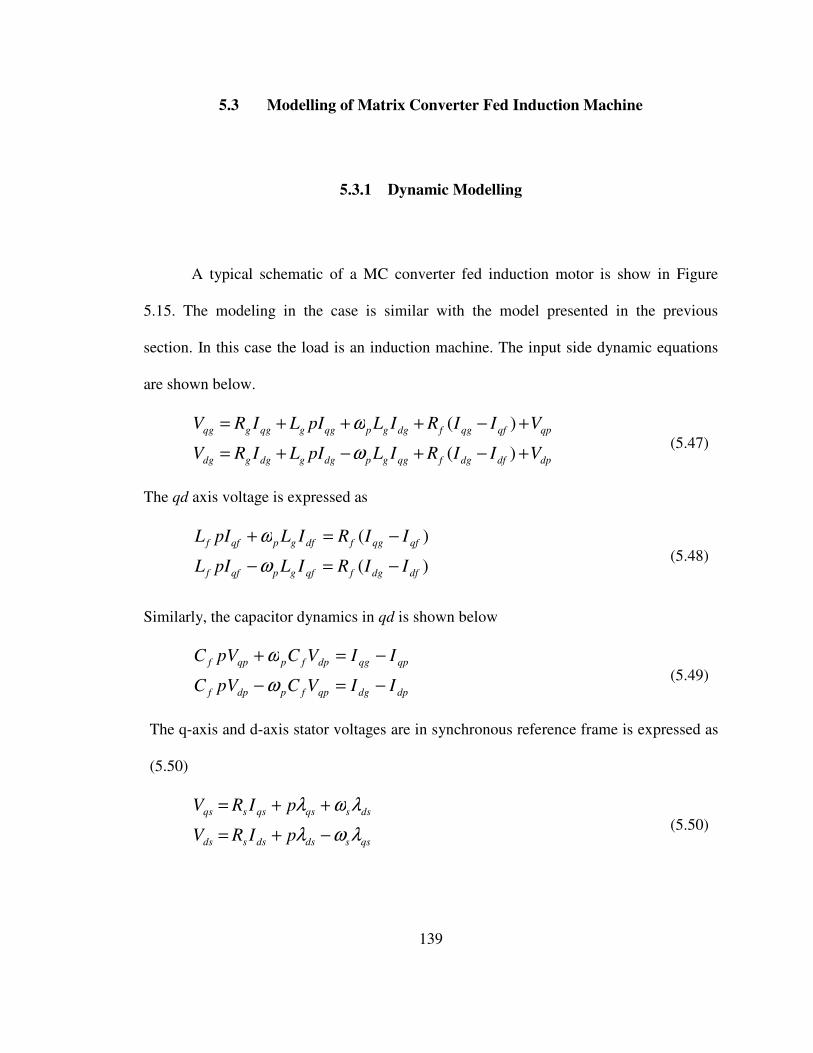
139
5.3 Modelling of Matrix Converter Fed Induction Machine
5.3.1 Dynamic Modelling
A typical schematic of a MC converter fed induction motor is show in Figure
5.15. The modeling in the case is similar with the model presented in the previous
section. In this case the load is an induction machine. The input side dynamic equations
are shown below.
dpdfdgfqggpdggdggdg
qpqfqgfdggpqggqggqg
VIIRILpILIRV
VIIRILpILIRV
+−+−+=
+−+++=
)(
)(
ω
ω (5.47)
The qd axis voltage is expressed as
)(
)(
dfdgfqfgpqff
qfqgfdfgpqff
IIRILpIL
IIRILpIL
−=−
−=+
ω
ω (5.48)
Similarly, the capacitor dynamics in qd is shown below
dpdgqpfpdpf
qpqgdpfpqpf
IIVCpVC
IIVCpVC
−=−
−=+
ω
ω (5.49)
The q-axis and d-axis stator voltages are in synchronous reference frame is expressed as
(5.50)
qssdsdssds
dssqsqssqs
pIRV
pIRV
λωλ
λωλ
−+=
++= (5.50)

140
Figure 5.14 Schematic diagram of the AC/AC matrix converter fed induction motor
In squirrel cage type induction machine with shorted rotor, the rotor voltages are zero and
expressed as
( )
( ) '''''
'''''
0
0
qrrsdrdrrdr
drrsqrqrrqr
pIRV
pIRV
λωωλ
λωωλ
−−+==
−++== (5.51)
The expressions for q-axis and d-axis stator flux linkages are given as:
'
'
drmdssds
qrmqssqs
ILIL
ILIL
+=
+=
λ
λ (5.52)
The q-axis and d-axis rotor flux linkages are expressed as:

141
'''
'''
drrdsmdr
qrrqsmqr
ILIL
ILIL
+=
+=
λ
λ (5.53)
The electromagnetic torque is expressed in terms of the stator flux linkage and stator
current as given in (5.54). This torque is positive for motor action and negative in
generating mode.
( )dsqsqsdse II
PT λλ −=
4
3 (5.54)
The rotor speed and electromagnetic torque of a P pole machine are related by (5.55)
where J is the inertia of the rotor and connected mechanical load expressed in kgm2. TL is
the load torque.
( )Ler TTJ
Pp −=
2ω (5.55)
5.3.2 Dynamic Simulation Results and Discussion
Simulation of the system is developed based on the model equations (5.48) to
(5.55) using the parameters given in Table 5.1. The motor starts at no load so as to
observe the starting transient and then a 25 Nm load torque are applied after 0.5 s to show
the dynamic response of the system. At starting, the motor experiences high
electromagnetic torque with rising rotor speed until they both reach their steady values
after 0.3 s as seen in Figure 5.15. These figures also show the responses for a step change
of load at 0.6 s. The output line-to-line and phase voltages of the converter are both
average sinusoidal waveforms as shown in Figure 5.16.

142
Figure 5.15 Starting transient and dynamic response of (a) rotor speed and (b)
electromagnetic torque
Figure 5.16 MC output (a) line-to-line voltage (b) phase voltage
0 0.1 0.2 0.3 0.4 0.5 0.6 0.7 0.80
100
200
300
ωr [
rad/s
ec]
(a)
0 0.1 0.2 0.3 0.4 0.5 0.6 0.7 0.8
0
50
100
Te [
Nm
]
Time [sec] (b)
0.74 0.75 0.76 0.77 0.78 0.79 0.8
-500
0
500
Vab [
V]
(a)
0.74 0.75 0.76 0.77 0.78 0.79 0.8-400
-200
0
200
400
Vas [
V]
Time [sec] (b)

143
Figure 5.17 (a) Input capacitor phase voltage (b) filtered capacitor voltage
Figure 5.18 (a) MC input phase current (b) source phase current
The input capacitor voltages before and after the digital filter are given in Figure
5.17. It clearly verify that the digital low pass filter implemented in qd-synchronous
0.74 0.745 0.75 0.755 0.76 0.765 0.77 0.775 0.78 0.785 0.79
-200
0
200
Vap [
V]
(a)
0.74 0.745 0.75 0.755 0.76 0.765 0.77 0.775 0.78 0.785 0.79
-200
0
200
Vaf [
V]
Time [sec] (b)
0.74 0.745 0.75 0.755 0.76 0.765 0.77 0.775 0.78 0.785 0.79-20
-10
0
10
20
I ap [
A]
(a)
0.74 0.745 0.75 0.755 0.76 0.765 0.77 0.775 0.78 0.785 0.79
-10
-5
0
5
10
I ag [
A]
Time [sec] (b)

144
reference frame eliminate higher order harmonics resulting in a relatively pure sinusoidal
voltage which is used to generate the modulation signals.
5.3.3 Generalized Steady State Analysis
This section presents a generalized steady state analysis for matrix converter fed
induction machine. With similar approaches shown in section 5.1.3, steady state the q-
axis and d-axis voltage equations of the source are expressed as
dpdfdgfqggpdggdg
qpqfqgfdggpqggqg
VIIRILIRV
VIIRILIRV
+−+−=
+−++=
)(
)(
ω
ω (5.56)
And the voltage equations for the inductor voltage at steady state
)(
)(
dfdgfqffp
qfqgfdffp
IIRIL
IIRIL
−=−
−=
ω
ω (5.57)
The q-axis and d-axis voltage equations for the inductor voltage at steady state is given as
dsddqsqddgqpfp
dsdqqsqqqgdpfp
IMIMIVC
IMIMIVC
−−=−
−−=
ω
ω (5.58)
The active and reactive power of the drawn from the source can be represented in terms
of the synchronous reference frame voltages and currents as follows.
)(2
3
)(2
3
qgdgdgqgg
dgdgqgqgg
IVIVQ
IVIVP
−=
+=
(5.59)

145
The q-axis and d-axis stator voltages are given as:
qssdssds
dssqssqs
IRV
IRV
λω
λω
−=
+= (5.60)
Rotor voltage steady state equations
( )
( ) ''''
''''
0
0
qrrsdrrdr
drrsqrrqr
IRV
IRV
λωω
λωω
−−==
−+== (5.61)
The expressions for q-axis and d-axis stator flux linkages are given as:
'
'
drmdssds
qrmqssqs
ILIL
ILIL
+=
+=
λ
λ (5.62)
The q-axis and d-axis rotor flux linkages are expressed as:
'''
'''
drrdsmdr
qrrqsmqr
ILIL
ILIL
+=
+=
λ
λ (5.63)
In matrix form
−−
−−=
dr
qr
ds
qs
rrsms
rsrms
mssss
mssss
ds
qs
I
I
I
I
RLsLs
LsRLs
LRL
LLR
V
V
ωω
ωω
ωω
ωω
0
0
0
0
0
0 (5.64)
The electronic torque is expressed in terms of the stator flux linkage and stator current as
given in (). This torque is positive for motor action and negative in generating mode.
( )dsqsqsdse II
PT λλ −=
4
3 (5.65)
The rotor speed and electromagnetic torque of a P pole machine are related by (5.65)
where J is the inertia of the rotor and connected mechanical load expressed in kgm2. TL is
the load torque.

146
( )Ler TTJ
Pp −=
2ω (5.66)
The steady state variables are computed step-by-step as follows:
02 =++ cbMaM dddd (5.67
ddxdq MggMM 21−=
ds
qsddqd
V
VMM =
qd
dd
dqqq M
M
MM =
)(11 dsddqsqdqgqp IMIMgVkV ++=
)(43 qpqgqg VVI −= ββ
qgdg II ρ=
)(4 qpqgdp VVV −= β
qgqf II 1β= qgdf II 2β=
dsqsqs VmVmI 21 −= dsqsds VmVmI 12 +=
The constants used in the above expressions are given below:
)))(( 4211 dsdsqsqs IVIVggga ++= β ( ) dsqgVVggggkggkb )()( 2142114211 +−++= ββ
qgdsxds VVMkVc 1
2 −= dsdsqsqs
dsqg
xIVIV
kVVgM
+
−=
)1( 12
fp Cg
ωβρβ −−=
43
1
1 4432 βωββ fp Cg −=
f
fpf
fpfR
LR
LR
2221ω
ρωβ
+
−=
f
fpf
fpfR
LR
LR
2222ω
ωρβ
+
+=
))((
1
2
3
fgfgp RRRL +−+=
ρβωβ
))1((
1
13
4
gpfg LRR ρωβββ
+−+=
)(1 222222
1 rmsrssrs RLsLsRRRm ωω ++∆
= fpC
kωβρβ
βρβ
−=
43
43
1
)( 2222222
2 rmsrssrs
s LLsLsLRLm ωωω
−+∆
=
))(tan(cos 1 pf−=ρ
147
5.3.4 Steady State Simulation Results and Discussions
To verify the steady state performance of the induction motor drive, calculations are
done based on the model equations (5.56) to (5.67) with the parameters given in Table
5.1. Figures 5.19 - 5.19 are drawn considering lagging, unity and leading input power
factor operations. The torque-slip characteristics of the motor are shown in Figure 5.19
for different input power factor operations. This figure also shows that the
electromagnetic torque does not depend on the input power factor. Figure 5.20 gives the
magnitudes of the input capacitor voltage and source current. It can be observed that
when the drive operates at lagging input power factor, the speed range is very narrow
because of the limit in the matrix converter voltage transfer ratio. However, when the
overall system operates in leading and unity power factor, the matrix converter voltage is
below the maximum allowable limit in all possible speed ranges as seen in Figure 5.22.
The fundamental reason is demonstrate in Figure 5.20, when the system operate in
leading power factor mode, the magnitude of the input capacitor voltage will significantly
increased to inject reactive power to the source. As a result, it is possible to keep the
output stator voltage at the required value within the limit. On the other hand, in lagging
power factor operation, the capacitor voltage relatively lower value. Therefore, it is not
possible to get the specified stator voltage for wide load ranges; otherwise it goes to
unwanted over modulation region. The input active and reactive powers are shown in
Figure 5.21.

148
Figure 5.19 Steady state torque-slip characterstics of an induction machine
Figure 5.20 Magnitude of capacitor voltage and (b) magnitude of source current
50 100 150 200 250 3000
10
20
30
40
50
60
70
ωr [rad/sec]
Te [
Nm
]
0.85 leading
unity
0.85 lagging
50 100 150 200 250 300200
250
300
350
(a)
Vp [
V]
50 100 150 200 250 3000
20
40
60
ωr [rad/sec] (b)
I g [
A]
0.85 leading
unity
0.85 lagging

149
Figure 5.21 (a) Active power and (b) reactive power drawn from the source
Figure 5.22 Effect of input and output power factors on (a) voltage ratio and (b)
magnitude of modulation index
50 100 150 200 250 3000
5
10
15
20
(a)
Pin
[kW
]
50 100 150 200 250 300-15
-10
-5
0
5
ωr [rad/sec] (b)
Qin
[kV
ar]
0.85 leading
unity
0.85 lagging
50 100 150 200 250 3000.4
0.6
0.8
1
(a)
Voltage r
atio (
Vs/V
p)
50 100 150 200 250 300
0.8
0.9
1
ωr [rad/sec] (b)
M
0.85 leading
unity
0.85 lagging

150
Table 5.1 System Parameters
RL Load parameters
Vs = 220V(rms) fs = 50Hz Rs = 10Ω Ls =20mH
Source and filter parameters
Vg = 380V(rms) fp = 60Hz Rg = 0.5Ω, Lg = 1mH
Rf = 30Ω Lf = 7.46mH Cf = 10µF
Induction machine parameters
Vs = 220Vrms fs = 50Hz Rs = 0.531Ω Rr = 0.408Ω
Ls = 87.22mH Lr = 87.22mH Lm = 85.7mH J = 0.04kg.m2 P = 4
5.4 Conclusion
A modeling of the AC/AC matrix converter feeding an RL load is presented. A
new generalized steady state analysis is developed which avoid the constraint of
operating at input unity power factor. Simulation has been done to verify the theoretical
analysis. Results show that with matrix converter, it is possible to control the input and
output power factor independently. With a similar approach, dynamic and steady state
analysis are developed for matrix converter fed induction motor system. Computer
simulation results clearly show the starting transient and the dynamic response to a
sudden change of the load during the steady state operation. The steady state analysis of
the complete system is also laid out clearly along with the plots of the performance
characteristics of the system.

151
CHAPTER 6
STABILITY ANALYSIS FOR A MATRIX CONVERTER FED
INDUCTION MOTOR
6.1 Introduction
This chapter investigates issues related to instabilities in a matrix converter fed
drive system. The presence of the input LC filter along with the direct coupling nature of
the matrix converter may lead to unstable operation when the power delivered exceeds a
certain limit value.
A new generalized model for stability analysis based on a small signal modeling
is proposed, for matrix converter fed induction motor drive system. A small signal model
of the overall drive system is also presented in synchronous reference frame. It is
necessary to note that the stability analysis does not include the mechanical dynamics as a
result it can also be known as electrical stability analysis. The stability of the system is
evaluated by analyzing the migration of eigen values of the system, which is linearized
around the operating point. The generalized steady state analysis is also presented to
provide the operating points for stability analysis as well as to study the steady state
performance of the system under constant Volt per Hertz (V/F) operation.

152
This approach considers the analysis when the drive system operates at unity as
well as non-unity input power factor at the source side. With the help of this model,
different factors which affect the matrix converter stability are analyzed including stator
and rotor resistance variation due to motor heating and the impact of non-zero reactive
power at the source side. The paper also presents a complete and a general steady state
analysis in the q-d synchronous reference frame when the whole drive system operates
under a constant Volt/Hertz operation. Computer simulations are carried out to verify
theoretical analysis on stability as well as on the steady state performance characteristics
6.2 Modeling of the Drive System
The complete modelling of the studied system shown in Figure 6.1 is presented
section 5.3. The input voltage equations in a synchronous reference frame are shown as.
dpdfdgfqggpdggdggdg
qpqfqgfdggpqggqggqg
VIIRILpILIRV
VIIRILpILIRV
+−+−+=
+−+++=
)(
)(
ω
ω (6.1)
The voltage drop in the filter inductor can be represented as
)(
)(
dfdgfqfgpqff
qfqgfdfgpqff
IIRILpIL
IIRILpIL
−=−
−=+
ω
ω (6.2)
The dynamic equation of filter capacitor is given by,
dpdgqpfpdpf
qpqgdpfpqpf
IIVCpVC
IIVCpVC
−=−
−=+
ω
ω (6.3)

153
Figure 6.1 Schematic diagram of the AC/AC matrix converter fed induction motor
The q-axis and d-axis stator voltages are
qssdsdssds
dssqsqssqs
pIRV
pIRV
λωλ
λωλ
−+=
++= (6.4)
In squirrel cage type induction machine with shorted rotor, the rotor voltages are zero and
expressed as
( )
( ) qrrsdrdrrdr
drrsqrqrrqr
pIRV
pIRV
λωωλ
λωωλ
−−+==
−++==
0
0 (6.5)

154
The expressions for q-axis and d-axis stator flux linkages are given as:
drmdssds
qrmqssqs
ILIL
ILIL
+=
+=
λ
λ (6.6)
The q-axis and d-axis rotor flux linkages are expressed as:
drrdsmdr
qrrqsmqr
ILIL
ILIL
+=
+=
λ
λ (6.7)
The electronic torque is expressed in terms of the stator flux linkage and stator current as
given in (4.54). This torque is positive for motor action and negative in generating mode.
( )dsqsqsdse II
PT λλ −=
4
3 (6.8)
The rotor speed and electromagnetic torque of a P pole machine are related by (6.9)
where J is the inertia of the rotor and connected mechanical load expressed in kgm2. TL is
the load torque.
( )Ler TTJ
Pp −=
2ω (6.9)
The digital filter dynamics in synchronous reference frame are
)(1
)(1
dfdpdf
qfqpqf
VVpV
VVpV
−=
−=
τ
τ (6.9)
The mapping between the input current and output current using the components of the
modulation signals are
dsddqsqddp
dsdqqsqqqp
IMIMI
IMIMI
+=
+= (6.10)

155
Similarly, the output voltage can be expressed in terms of the input voltage and
modulation signals as follow.
dpddqpdqds
dpqdqpqqqs
VMVMV
VMVMV
+=
+= (6.11)
Equation in (6.1) can be rearranged as follows
( )
( )dpqggpdffdgfgdg
g
dg
qpdggpqffqgfgqg
g
qg
VILIRIRRVL
pI
VILIRIRRVL
pI
−+++−=
−−++−=
ω
ω
)(1
)(1
(6.12)
Similarly, the filter current dynamics can be expressed as
( )
( )dffqffpdgf
f
df
dffpqffqgf
f
qf
IRILIRL
pI
ILIRIRL
pI
−+=
−−=
ω
ω
1
1
(6.13)
Substituting (6.10) into (6.3)
( )
( )dsddqsqdqpfpdg
f
dp
dsdqqsqqdpfpqg
f
qp
IMIMVCIC
pV
IMIMVCIC
pV
−−+=
−−−=
ω
ω
1
1
(6.14)
)(1
)(1
dfdpdf
qfqpqf
VVpV
VVpV
−=
−=
τ
τ (6.15)
The q-axis stator and the rotor currents can be written in terms of the stator and rotor flux
linkages as follows.
)( qrmqsrs
qs LLD
rI λλ −= (6.16)

156
)( qrsqsmr
qr LLD
rI λλ +−= (6.17)
where the
2
mrs LLLD −= (6.18)
Similarly, the d-axis stator and the rotor currents can be written in terms of the stator and
rotor flux linkages as follows.
)( drmdsrs
ds LLD
rI λλ −= (6.19)
)( drsdsmr
dr LLD
rI λλ +−= (6.20)
Substituting (6.61-6.19) into (6.4) and (6.5), the induction motor dynamics can be written
in terms of only the stator flux linkages. From the stator voltage equations, the dynamics
of the stator flux linkage can be written as
qsedrms
dsrs
dpddqpdqds
dseqrms
qsrs
dpqdqpqqqs
D
Lr
D
LrVMVMp
D
Lr
D
LrVMVMp
λωλλλ
λωλλλ
++−+=
−+−+=
(6.21)
Similarly, the rotor flux dynamics can be represented as
qrsodrsr
dsmr
dr
drsoqrsr
qsmr
qr
D
Lr
D
Lrp
D
Lr
D
Lrp
λωλλλ
λωλλλ
+−=
−−= (6.22)

157
6.3 Small Signal Analysis
This section discusses the stability of the model given in Figure 6.1. The small
signal analysis of the system is done to determine the stability limit under constant volts
per hertz (V/f) operation. To determine the small signal model of the system, it should be
first linearized around the operating point. Therefore each state are defined by the
operating points
XXX o ∆+= (6.23)
And the inputs and the disturbances are
UUU o ∆+= (6.48)
where
=
dd
dq
qd
M
M
M
M
U
=
ddo
dqo
qdo
qqo
o
M
M
M
M
U
∆
∆
∆
∆
=∆
dd
dq
qd
M
M
M
M
U
[ ]Tdrqrdsqsdfqfdpqpdfqfdgqg VVVVIIIIX λλλλ=
[ ]Tdroqrodsoqsodfoqfodpoqpodfoqfodgoqgoo VVVVIIIIX λλλλ=
[ ]Tdrqrdsqsdfqfdpqpdfqfdgqg VVVVIIIIX λλλλ ∆∆∆∆∆∆∆∆∆∆∆∆=∆

158
The linearization of the system dynamics around steady state operating point leads to the
following small signal model of the system.
( )qpdggpqffqgfgqg
g
qg VILIRIRRVL
Ip ∆−∆−∆+∆+−∆=∆ ω)(1
(6.24)
( )dpqggpdffdgfgdg
g
dg VILIRIRRVL
Ip ∆−∆+∆+∆+−∆=∆ ω)(1
(6.25)
( )dffpqffqgf
f
qf ILIRIRL
Ip ∆−∆−∆=∆ ω1
(6.26)
( )dffqffpdgf
f
df IRILIRL
Ip ∆−∆+∆=∆ ω1
(6.27)
( )dqdsoqqqsodsdqoqsqqodpfpqg
f
qp MIMIIMIMVCIC
Vp ∆−∆−∆−∆−∆−∆=∆ ω1
(6.28)
( )dddsoqdqsodsddoqsqdoqpfpdg
f
dp MIMIIMIMVCIC
Vp ∆−∆−∆−∆−+∆=∆ ω1
(6.29)
)(1
qfqpqf VVVp ∆−∆=∆τ
(6.30)
)(1
dfdpdf VVVp ∆−∆=∆τ
(6.31)
dseqrms
qsrs
qddpqqqpdpqdqpqqqs
D
Lr
D
Lr
MVMVVMVMp
λωλλ
λ
∆−∆+∆
−∆+∆+∆+∆=∆ 00
(6.32)

159
qsedr
ms
ds
rs
dddpodqqpodpddqpdqds
D
Lr
D
Lr
MVMVVMVMp
λωλλ
λ
∆+∆+∆
−∆+∆+∆+∆=∆
(6.33)
drsoqr
sr
qs
mr
qrD
Lr
D
Lrp λωλλλ ∆−∆−∆=∆ (6.34)
qrsodr
sr
ds
mr
drD
Lr
D
Lrp λωλλλ ∆+∆−∆=∆ (6.35)
By resolving (6.24)-(6.35), the state equations is given as
BUAXpX +=
In the above state space representation, the inputs are the modulation signals.
Since the operating conditions are computed for a specified stator voltage of the
induction motor, it is possible to change the inputs from the modulation signals to the
stator voltage. Define the four components of the components of the modulation signals
as follows. It is necessary to note that these modulation signals depend on the filtered
capacitor voltage and output voltage.
22
dfqf
qfqs
qqVV
VVM
+= (6.36)
22
dfqf
dfqs
qdVV
VVM
+= (6.37)
22
dfqf
qfds
dqVV
VVM
+= (6.38)
22
dfqf
dfds
ddVV
VVM
+= (6.39)

160
Applying small signal analysis on (6.36)-(6.39), the operating point modulation signals can
separately represented in terms of the operating point filter input capacitor voltage and
output voltage.
2
fo
qfoqso
qqoV
VVM = (6.40)
2
fo
dfoqso
qdoV
VVM = (6.41)
2
fo
qfodso
dqoV
VVM = (6.42)
2
fo
dfodso
ddoV
VVM = (6.43)
At steady state, the input capacitor voltage before and after low pass filter is the same.
Substituting (6.44)-(6.47) into (6.28), (6.29), (6.32) and (6.33), the system characteristic
matrix is given in (6.50).
qs
dfoqfo
qfo
df
dfoqfo
dfoqfoqso
qf
dfoqfo
qfodfoqso
qq VVV
VV
VV
VVVV
VV
VVVM ∆
++∆
+−∆
+
−=∆
22222222
22
)(
2
)(
)( (6.44)
qs
dfoqfo
dfo
df
dfoqfo
dfoqfoqso
qf
dfoqfo
dfoqfoqso
qd VVV
VV
VV
VVVV
VV
VVVM ∆
++∆
+
−+∆
+−=∆
22222
22
222)(
)(
)(
2 γγγ (6.45)
ds
dfoqfo
qfo
df
dfoqfo
dfoqfodso
qf
dfoqfo
qfodfodso
dq VVV
VV
VV
VVVV
VV
VVVM ∆
++∆
+−∆
+
−=∆
22222222
22
)(
2
)(
)( γγγ (6.46)
ds
dfoqfo
dfo
df
dfoqfo
dfoqfodso
qf
dfoqfo
dfoqfodso
dd VVV
VV
VV
VVVV
VV
VVVM ∆
++∆
+
−+∆
+−=∆
22222
22
222 )(
)(
)(
2 γγγ (6.47)

161
−
−−
−−−
−−−−
−
−
−
−
−−
−+
−
−−+
−
=
D
LR
D
LRD
LR
D
LRD
LR
D
LRxxxx
D
LR
D
LRxxxx
C
x
C
xyy
C
C
x
C
xyy
C
L
R
L
R
L
R
L
R
LL
R
L
RR
LL
R
L
RR
A
srso
mr
sosrmr
msrse
mse
rs
ff
p
f
ff
p
f
f
f
p
f
f
p
f
f
f
f
gg
f
g
fg
p
gg
f
p
g
fg
ω
ω
ω
ω
ττ
ττ
ω
ω
ω
ω
ω
ω
000000000
000000000
00000
00000
00001
01
00000
000001
01
0000
000001
0
0000001
000000000
000000000
0000001
00
00000001
0
4343
2121
4343
2121
(6.50)
The constants represented in the matrix are computed at the steady state operation.
21
po
qpoqso
V
VVx −=
22
po
dpoqso
V
VVx −=
23
po
qpodso
V
VVx −=
24
po
dpodso
V
VVx −=
4
22
41
)(1
po
dpoqpo
f V
kVV
Cyy
−=−=
432
21
po
dpoqpo
f V
kVV
Cyy ==
dsodsoqsoqso IVIVk +=

162
The eigen-values can be found by evaluating the determinant of |SI - A| = 0, where the
matrix A is given in (6.50). There are 12 eigen values in which 10 of them always have
negative real parts regardless of the operating points; therefore, the rest two identical
dominant eigen values are used for determining stability limits. The graphs shown in this
section are obtained by varying the output and slip frequencies and collecting the
operating points which give zero real part of the dominant eigen values. It is necessary to
note that this eigen-value depends on the operating points. In [40], it is assumed that the
initial angles of the capacitor and reference voltages are zero, but in this analysis there is
no assumption made so that it is possible to study the effect non-zero reactive power at
the source on the stability of the system.
6.4 Simulation Results and Discussions
A matrix converter-induction motor system with parameters given in Table I, are
considered and the results of the stability analysis are given in Figure 6.2 to Figure 6.6 in
which the regions above the curves are the instability regions. As seen in Figure 6.2, a
significant improvement can be achieved using a low pass filter to the input capacitor
voltage. The influences of each factor on the stability are analyzed by adjusting only one
of them and keeping the other factors constant. As seen in Figure 6.3, in some regions of
load there is a limit on the maximum allowable output frequency to keep the system
stable. The figure also demonstrates that it is possible to improve the output frequency
limit by increasing the filter time constant, though the higher the time constant, the
slower the system response would be. The effect of the damping resistance is also
163
observed in Figure 6.4 Choosing a lower resistance value draws the high frequency
components of the input current and hence improves the stability of the system. However,
if this resistance is too small, the power loss in the damping resistance becomes very
significant at a low frequency.
The impact of the stator and rotor resistance variation on drive stability analysis is
also considered in this paper. For demonstration, the rotor resistance is varied by 40%
and 80% while the stator resistance increases by 20% and 40% since the rotor heating
affects the value of rotor resistance more than the value of stator resistance. Hence Rs2 =
1.2Rs, Rs2 = 1.4Rs, Rr2 = 1.4Rr, and Rr3 = 1.8Rr are selected for the analysis. From the
result seen in Figure 6.5, these resistance variations expand the stability margins. It was
noted that the rotor resistance variation is crucial in the design of high performance
induction motor control algorithms where the flux observers require the exact knowledge
of the rotor resistance [74]. However, regarding the stability of the system, it is not a
crucial issue. In Figure 6.6, the impact of non-zero reactive power on the matrix
converter stability is given. The result clearly shows that the system has better stability
region when the matrix converter operates with a leading power factor than with a
lagging power factor under the given input filter parameters. Therefore, in applications
where the matrix converter is used as a reactive power compensator, the stability region
is improved. However, when the converter operates at source lagging power, the drive
system becomes more stable with increasing in power factor.

164
Figure 6.2 Stability limit of matrix converter gain against filter time constant
Figure 6.3 Matrix converter stability limit for varying Filter time constant
τ [ms]
Voltage r
atio,
Vs/V
p
0.05 0.1 0.15 0.2 0.25 0.3 0.35 0.4 0.45 0.5
0.1
0.2
0.3
0.4
0.5
0.6
0.7
0.8
Stable region
Unstable region
f s [
Hz]
fso
[Hz]
5 10 15 20 25 30
5
10
15
20
25
30
35
40
45
50
Stable Region
Unstable Regionτ=0.3ms
τ=0.2msτ=0.1ms

165
Figure 6.4 Stability limit of the matrix converter for varying damping resistance
Figure 6.5 The impact of Stator and rotor resistance on the stability of the system
f s [
Hz]
fso
[Hz]
5 10 15 20 25 30
5
10
15
20
25
30
35
40
45
50
Stable region
Unstable region
Rf=30Ω
Rf=20Ω
Rf=40Ω
f s [
Hz]
fso
[Hz]
5 10 15 20 25 30
5
10
15
20
25
30
35
40
45
50
Stable region
Unstable region
Rs1
, Rr1
Rs3
, Rr3
Rs2
, Rr2

166
Figure 6.6 The impact of power factor on the stability of the system
The verification of the region of instability is done by a computer simulation
using motor and filter parameters given in Table I. The motor starts at no load so as to
observe the starting transient and then a 15 Nm load torque is applied after it reaches the
steady state at 0.5sec to show the electrical dynamic response of the system which is not
included in the figure. At starting, the motor experiences high electromagnetic torque
with rising rotor speed until they both reach their steady state values at 0.5sec as seen in
Figure 6.7. At this point the system operating at 50Hz output frequency and 1.5 Hz slip
frequency which is in the stable region as shown in Figure 6.3 when τ = 2 m sec . Then
the slip frequency is increased to 7Hz to operate in the unstable region after 0.8 sec. It is
necessary to note that both these points are taken in a linear region of torque-speed curve
of the motor, P1 and P2 as seen Figure 6.10.
f s [
Hz]
fso
[Hz]
5 10 15 20 25 30
5
10
15
20
25
30
35
40
45
50
Unstable region
0.7 leading
0.9 leading
Unity
0.9 lagging
0.7 lagging Stable region

167
Figure 6.7 (a) Rotor speed and (b) electromagnetic torque
Figure 6.8 Output line to line voltage and (b) input capacitor phase voltage
0 0.1 0.2 0.3 0.4 0.5 0.6 0.7 0.8 0.9 10
200
400
ωr [
rad/s
ec]
(a)
0 0.1 0.2 0.3 0.4 0.5 0.6 0.7 0.8 0.9 1
0
50
100
Te [
Nm
]
Time[sec] (b)
0.75 0.8 0.85 0.9 0.95
-1000
-500
0
500
1000
Vab [
V]
(a)
0.75 0.8 0.85 0.9 0.95
-500
0
500
Vap [
V]
Time[sec] (b)

168
Figure 6.9 MC input phase current and (b) source phase current
6.5 Steady State Operating Conditions
The steady state performance characteristic of the drive system is done to provide the
operating points for the electrical stability of the system as well as to study the
performance characteristics of the drive under constant Volt/Hertz operation. The steady-
state operating points of the system are determined from the system dynamic equations.
For the analysis, the input side reference frame angle is aligned to the q-axis of the source
voltage, such that Vdg = 0. This model is general which can be used either when the
source draws unity power factor or non-zero reactive power by giving proper value of the
power factor, pf. These operating points are evaluated first by calculating the Mdd from
(6.51) and all other variables can be found consecutively from (6.52) to (6.62).
0.75 0.8 0.85 0.9 0.95
-20
0
20
I ap [
A]
(a)
0.75 0.8 0.85 0.9 0.95-50
0
50
I ag [
A]
Time[sec] (b)

169
02 =++ cbMaM ddoddo (6.51
ddoxdqo MggMM 21−= (6.52)
dso
qso
ddoqdoV
VMM = (6.53)
qdo
ddo
dqo
qqo MM
MM = (6.54)
)(11 dsoddoqsoqdoqgqpo IMIMgVkV ++= (6.55)
)(43 qpoqgqgo VVI −= ββ (6.56)
qgodgo II ρ= (6.57)
)(4 qpoqgdpo VVV −= β (6.58)
qgoqfo II 1β= (6.59)
qgodfo II 2β= (6.60)
dsoqsoqso VmVmI 21 −= (6.61)
dsoqsodso VmVmI 12 += (6.62)
The constants used in the above expressions are given below:
)))(( 4211 dsdsqsqs IVIVggga ++= β
( ) dsqgVVggggkggkb )()( 2142114211 +−++= ββ

170
qgdsxds VVMkVc 12 −=
dsdsqsqs
dsqgx
IVIV
kVVgM
+
−=
)1( 12
fpCg
ωβρβ −−=
431
1
4432 βωββ fpCg −=
f
fpf
fpfR
LR
LR
2221ω
ρωβ
+
−=
f
fpf
fpfR
LR
LR
2222ω
ωρβ
+
+=
))((
1
23
fgfgp RRRL +−+=
ρβωβ
))1((
1
134
gpfg LRR ρωβββ
+−+=
)(1 222222
1 rmsrssrs RLsLsRRRm ωω ++∆
=
)( 2222222
2 rmsrssrs
s LLsLsLRLm ωωω
−+∆
=
fpCk
ωβρβ
βρβ
−=
43
431
))(tan(cos 1
pf−=ρ
6.6 Simulation Result for Volt/Hz Control
The result of the steady state performance is demonstrated in Figure 6.10 to
Figure 6.13 under a unity power factor operation. These results also compared with
simulation results given in Figure 6.7. Figure 6.10 shows how the torque speed curves of
the induction motor vary with the stator frequencies under constant volt/Hertz operation.
These results also validate the simulation results given in Figure 6.7 where the angular
speed goes to 307rad/sec after applying 15Nm during stable operation at P1. Further
increasing the load to 45Nm reduces the rotor speed to 288rad/sec at P2 which leads to a

171
drive system oscillation. It is clearly seen that these two operating points are in the linear
torque region. Since the stator voltage is not constant resulting in a variable capacitor
voltage, the source current will also corresponding vary as shown in Figure 6.11. This
figure also verified the result in Fig 5c where the source current is about 13A at
307rad/sec. With the constant voltage source, the gain is directly proportional to the
output frequency with V/f control as seen in Figure 6.12. As verified in Figure 6.13,
when the source draws a unity power factor current, it is certain that the power factor at
the input of the converter will no longer be unity due to the reactive power generated in
the filter circuit. Therefore these results verify that under unity power factor operation at
the source side it is not correct to make the assumption on the phase angle of the
capacitor voltage to be zero.
Table 6.1 System parameters used in the stability study
Squirrel cage induction machine parameters
Vs = 220V(rms) fs = 50Hz, Rs = 0.531Ω,
Rr = 0.408Ω, Ls = 87.22mH, Lr = 87.22mH,
Lm = 84.7mH, J = 0.04kg.m2
, P = 4
Source and filter parameters
Vg = 380V(rms) fp = 60Hz,
Rg = 0.5Ω, Rf = 30Ω,
Lg = 1mH, Lf = 7.46mH, Cf = 10µF

172
Figure 6.10 Induction motor Electromagnetic torque
Figure 6.11 Magnitude of source current
0 50 100 150 200 250 3000
10
20
30
40
50
60
70
ωr
Te [
Nm
]
fs = 10Hz
fs = 30Hz
fs = 50Hz
P2
P1
0 50 100 150 200 250 3000
10
20
30
40
50
ωr
I g [
A]
fs = 10Hz
fs = 30Hz
fs = 50Hz

173
Figure 6.12 Converter voltage transfer ratio against rotor speed.
Figure 6.13 Ratio of reactive power to the apparent power at the input of the converter
0 50 100 150 200 250 300-0.6
-0.4
-0.2
0
0.2
0.4
0.6
0.8
1
ωr
Q/S
fs = 10Hz
fs = 30Hz
fs = 50Hz
0 50 100 150 200 250 3000.1
0.2
0.3
0.4
0.5
0.6
0.7
0.8
ωr
Voltage r
atio,
(Vs/V
p)
fs = 10Hz
fs = 30Hz
fs = 50Hz

174
6.7 Conclusion
A small signal electrical stability study of the AC/AC matrix converter fed induction
motor drive system is presented. This is determined from the small signal analysis of the
whole drive system operating under constant Volts/ Hertz operation. By analyzing the
real values of the dominant eigen values, the limit for stable operation has been
determined. It is also noticed that this stability limit is affected by different system
parameters including the input filter time constant and damping resistance. This work
also investigates the influence of reactive power exchange between the source and the
converter on the system stability in which the system is more stable when it operates with
a leading rather than a lagging power factor. The impact of stator and rotor resistance
variations on the converter stability is also studied and the results show that these
variations expand the stability regions. The proposed model clearly shows, through
computer simulation results the region of stable and unstable operations. The paper also
presents a generalized steady state model of the drive system which can be used for a
unity as well as non-unity power factor operations at the source. The analysis was
validated with computer simulation results which clearly show the performance
characteristics of the drive under unity input power factor operation. Clear comparison
between simulation and steady state results are presented.

175
CHAPTER 7
VECTOR CONTROL OF MATRIX CONVERTER FED
INDUCTION MACHINE
7.1 Introduction
In this chapter, the indirect rotor field oriented control (FOC) for matrix converter fed
induction machine is presented to realize the high performance control of the drive. The
control scheme proposed in this work also includes unity power factor control in the
source side. Induction motor drive fed by matrix converter is superior to the conventional
inverter based because of the lack of bulky direct current (dc)-link capacitors with limited
lifetime, bidirectional power flow capability, sinusoidal input/output currents, and
adjustable input power factor [67]. Besides, a matrix converter provides more degree of
freedom than the conventional voltage source inverter. Therefore, it is possible to control
additional variables such as reactive power in the input side.
The chapter is organized in different sections; the complete formulation of the
proposed control scheme in synchronous reference frame is presented in the first section.
An input-output feedback linearization is given to transform a nonlinear system into a
(fully or partially) linear system so as to use the well-known and powerful linear design
techniques to complete the control design. The control block consists of the rotor speed,
rotor flux and unity input power factor controllers. Besides, the q-axis component of the

176
rotor flux is controlled to assure rotor flux orientation. These involve separate control of
q-axis and d-axis stator currents, source current and input capacitor voltage.
The stator flux estimation which is later used to estimate the rotor fluxes is
presented. The control scheme involving nine controllers including the flux estimation is
simulated using Matlab/Simulink considering different speed trajectories and load
variation. Results verify the robustness of the proposed controllers. Finally the chapter is
summarized with a concluding remark.
7.2 Field Oriented Control for Matrix Converter Fed Induction Motor with
Unity Input Power Factor Control
The control scheme presented in the subsequent sections is categorized into two, the
FOC of the induction machine and input power factor control in the source side of the
matrix converter. In vector control, the rotor and stator fluxes have q-axis and d-axis
components like the voltage and currents. However, in rotor field orientation control, the
rotor flux linkage is aligned in the synchronous reference frame. As result, the rotor flux
is represented by a scalar instead of a phasor.
7.2.1 Indirect Field Oriented Control
This section presents the formulation of vector control scheme for the induction
motor.

177
Figure 7.1 Schematic diagram of the matrix converter fed induction motor without
damping resistor
It also provides detailed and step by step controllers designed to track the speed and
flux trajectories. The schematic of the drive system used in the control design is shown in
Figure 7.1.
The damping resistor is assumed to be big enough to be considered as open circuit.
As a result, the source and filter inductors are added together and represented as Lt. The
induction machine model equations are derived in section 5.3.1. The stator voltage
equations in synchronous reference frame are
qsedsdssds
dseqsqssqs
pIrV
pIrV
λωλ
λωλ
−+=
++= (7.1)
And the rotor voltages are expressed as follows where the rotor voltages are zero for a
squirrel cage induction machine.

178
qrsodrdrrdr
drsoqrqrrqr
pIRV
pIRV
λωλ
λωλ
−+==
++==
0
0 (7.2)
ωso , the slip frequency is given as the difference between the frequency of rotor flux
linkage and rotor speed.
Stator flux linkage are expressed as
drmdssds
qrmqssqs
ILIL
ILIL
+=
+=
λ
λ (7.3)
And the rotor flux linkage equations:
drrdsmdr
qrrqsmqr
ILIL
ILIL
+=
+=
λ
λ (7.4)
The rotor speed dynamics
( )Ler TTJ
Pp −=
2ω (7.5)
The developed electromagnetic torque can be written as different equations using four of
the eight components of the stator and rotor flux linkages and currents.
)(4
3
)(4
3
)(4
3
)(4
3
dsqrqsdr
s
m
qrdsdrqs
s
m
dsqrqsdr
r
m
dsqsqsdse
IIIIL
LP
IIL
LP
IIL
LP
IIP
T
−=
−=
−=
−=
λλ
λλ
λλ
(7.6)
The qdo voltage equations of the squirrel-cage induction motor can be modified to (7.7)
to have the stator current and rotor flux linkages in the expressions.

179
qr
r
mrrdr
r
mrqsedsdsds
dr
r
mrqr
r
mrdseqsqsqs
L
LR
L
LRILrIVpIL
L
L
L
LRILrIVpIL
λωλω
λωλω
σσ
σσ
++−−=
−+−−=
2
2
(7.7)
Similarly, based on the rotor voltage equations, the dynamic of the rotor flux linkages are
shown below.
qrsods
r
mr
dr
r
rdr
drsoqs
r
mr
qr
r
rqr
IL
LR
L
Rp
IL
LR
L
Rp
λωλλ
λωλλ
++−=
−+−=
(7.8)
Substituting the equation of the electromagnetic torque given in (7.6) into (7.5), the
modified rotor speed dynamics is shown below.
Ldsqrqsdrer TJ
PIIKp
2)( −−= λλω (7.9)
where
r
ms
L
LLL
2
−=σ , 2
2
r
mrs
L
LRRr += and
r
m
eL
L
J
PK
8
3 2
=
In the rotor flux orientation control, λqr = 0, the expression for the electromagnetic torque
can be modified to
qsdr
r
m
e IL
LPT λ
4
3= (7.10)
As shown in equation (7.10) if the q-axis rotor flux is regulated to be zero and the d-axis
flux is made constant, the electromagnetic torque is proportional to the q-axis stator
current. Therefore, the q-axis stator current is also known as a torque producing

180
component of the stator current. Since λqr = 0, rotor voltage equations are modified as
follows.
drdrr
drsoqrr
pIR
IR
λ
λω
+=
+=
0
0 (7.11)
Similarly, the rotor flux linkages are
drrdsmdr
qrrqsm
ILIL
ILIL
+=
+=
λ
0 (7.12)
From the above equations the rotor currents are expressed in (7.13); however, the rotor
currents are not generally known.
r
dsmdrdr
qs
r
mqr
L
ILI
IL
LI
−=
−=
λ (7.13)
At steady state the rotor flux linkage only depend on the d-axis current; therefore, this
component of the stator current is also known as magnetizing component. From (7.10)
and (7.14), it is possible to consider the induction machine as idealized DC machine for
the control purpose in which the d-axis current is analogous to the field current where as
the q-axis current is equivalent to the armature current of the separately exited dc
machine.
dsmdr IL=λ (7.14)
Substituting (7.13) into (7.11), the slip frequency can be given as
dr
qs
r
mrso
I
L
LR
λω =

181
0=−+ ds
r
mr
dr
r
rdr I
L
LR
L
Rp λλ (7.15)
Therefore, the induction machine dynamic equations for the system under rotor flux
oriented control are summarized below:
dr
r
mrqr
r
mrdseqsqsqs
L
L
L
LRILrIVpIL λωλω σσ −+−−=
2 (7.16)
qr
r
m
rdr
r
mr
qsedsdsdsL
L
L
LRILrIVpIL λωλω σσ +++−=
2 (7.17)
drsoqs
r
mr
qr
r
rqr I
L
LR
L
Rp λωλλ −+−= (7.18)
qrsods
r
mr
dr
r
rdr I
L
LR
L
Rp λωλλ ++−= (7.19)
Ldsqrqsdrer TJ
PIIKp
2)( −−= λλω (7.20)
7.2.2 Unity Input Power Factor Control
The second category of the proposed control scheme is unity input power factor
control. This is achieved by controlling the reactive power absorbed by the system to
zero; the drive system can only draw active power from the source. The unique advantage
of operating at unity input power factor in matrix converter driven system is that the
converter will operate with the maximum possible voltage transfer ratio. However, the
improvement in range of operation of a matrix converter operating at non-unity power
factor is presented in [67].

182
The expression for the input reactive power in synchronous reference frame is given
as
)(2
3qgdgdgqgg IVIVQ −= (7.21)
Aligning the source voltage in the q-axis of synchronous reference frame, Vdg = 0, and
Vqg = Vg where Vg is the peak value of source phase voltage. Therefore, the reactive
power expression only depends on the d-axis source current, Idg.
dgqgg IVQ2
3= (7.22)
By regulating Idg to zero, it is possible to maintain unity input factor and hence the
controller design technique developed in this section is totally based on this component
of the source current. The q-axis and d-axis voltage equations of the source are expressed
as
dpqgtpdgtdggdg
qpdgtpqgtqggqg
VILpILIRV
VILpILIRV
+−+=
+++=
ω
ω (7.23)
The q-axis and d-axis current equations for the filter capacitor
dpdgqpfpdpf
qpqgdpfpqpf
IIVCpVC
IIVCpVC
−=−
−=+
ω
ω (7.24)
The digital filter dynamics in synchronous reference frame are
)(1
)(1
dfdpdf
qfqpqf
VVpV
VVpV
−=
−=
τ
τ (7.25)
The mapping between the input current and output current using the components of the
modulation signals are derived in section as follows

183
dsddqsqddp
dsdqqsqqqp
IMIMI
IMIMI
+=
+= (7.26)
Similarly, the output voltage can be expressed in terms of the input voltage and
modulation signals as follow.
dpddqpdqds
dpqdqpqqqs
VMVMV
VMVMV
+=
+= (7.27)
The dynamic equations (7.16 - 7.27) are used to design the controllers.
7.2.3 Input-Output Feedback Linearization
The control design for induction machine is not easy due to the nonlinear nature of
the dynamic equations. There is no general method for designing nonlinear controllers;
however, there are alternative techniques which are best applicable for particular
nonlinear control problems [73]. Feedback linearization, Adaptive control and Gain
scheduling are commonly used nonlinear control design techniques. Feedback
linearization is developed in this chapter to transform the nonlinear system into a fully or
partly linear so that the linear control technique can be applied. This technique can be
considered as a tool for transforming a complex model into an equivalent model of
relatively simpler form.
In input-output linearization, a linear differential relation between the output and a
new input is generated by differentiating the output until there an input-output
relationship exists. And the second step is to formulate a controller based on the resulting
system. The number of differentiation required is known as relative order. If the relative
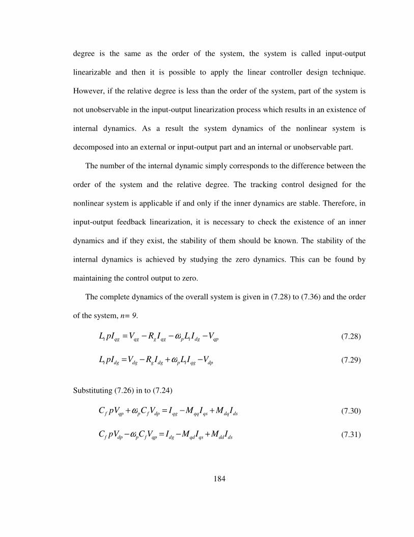
184
degree is the same as the order of the system, the system is called input-output
linearizable and then it is possible to apply the linear controller design technique.
However, if the relative degree is less than the order of the system, part of the system is
not unobservable in the input-output linearization process which results in an existence of
internal dynamics. As a result the system dynamics of the nonlinear system is
decomposed into an external or input-output part and an internal or unobservable part.
The number of the internal dynamic simply corresponds to the difference between the
order of the system and the relative degree. The tracking control designed for the
nonlinear system is applicable if and only if the inner dynamics are stable. Therefore, in
input-output feedback linearization, it is necessary to check the existence of an inner
dynamics and if they exist, the stability of them should be known. The stability of the
internal dynamics is achieved by studying the zero dynamics. This can be found by
maintaining the control output to zero.
The complete dynamics of the overall system is given in (7.28) to (7.36) and the order
of the system, n= 9.
qpdgtpqggqgqgt VILIRVpIL −−−= ω (7.28)
dpqgtpdggdgdgt VILIRVpIL −+−= ω (7.29)
Substituting (7.26) in to (7.24)
dsdqqsqqqgdpfpqpf IMIMIVCpVC +−=+ω (7.30)
dsddqsqddgqpfpdpf IMIMIVCpVC +−=−ω (7.31)

185
Using (7.27) into (7.16) and (7.17)
dr
r
mrqr
r
mrdseqsdpqdqpqqqs
L
L
L
LRILrIVMVMpIL λωλω σσ −+−−+=
2 (7.32)
qr
r
mrdr
r
mrqsedsdpddqpdqds
L
L
L
LRILrIVMVMpIL λωλω σσ +++−+=
2 (7.33)
The rotor flux and speed dynamics are represented as
drsoqs
r
mrqr
r
rqr I
L
LR
L
Rp λωλλ −+−= (7.34)
qrsods
r
mrdr
r
rdr I
L
LR
L
Rp λωλλ ++−= (7.35)
Ldsqrqsdrer TJ
PIIKp
2)( −−= λλω (7.36)
The objective is to control the speed and rotor flux linkage by orienting the flux in the
d-axis while maintaining a unity input power factor through the appropriate modulation
signals generated by the matrix converter. Looking at the overall system the input and
output of the nonlinear model is show in Figure 7.2.
=
dd
dq
qd
M
M
M
M
U
=
qr
dr
r
dgI
Y
λ
λ
ω
Figure 7.2 Control input and output of the system

186
The states, inputs and outputs of the system are,
[ ]T
rdrqrdsqsdpqpdgqg IIVVIIX ωλλ=
=
=
dd
dq
qd
M
M
M
M
u
u
u
u
U
4
3
2
1
=
=
qr
dr
r
dgI
y
y
y
y
Y
λ
λ
ω
4
3
2
1
To determine the existence of internal dynamics, the relative degree of the overall system
should be found. Since the system is a four input-four output, the relative degree
corresponding to each output should be computed first.
And by applying the superposition principle, the relative degree of the overall system is
the sum of the relative degree related with each output. The relative order for the first
control output, Idg is calculated as follows
dgIy =1
Differentiating the above output,
( )dpqgtpdggdg
t
dg VILIRVL
pIpy −+−== ω1
1
Since the input does not yet appear, differentiate the output for the second time result in

187
)(1
)(1
)(12
qpfpdsddqsqddg
tf
dpqgtpdgg
t
dpqgtpdggdg
t
dg
VCIMIMILC
pVpILpIRL
VILIRVL
pIp
ωω
ω
++−−+−−=
−+−=
Since the input appears after the second differentiation, the relative order for the first
output, r1 = 2. The relative order corresponding to the speed control is computed as
( )Ldsqrqsdrer
r
TIIKJ
Pppy
y
−−==
=
λλω
ω
22
2
Differentiating again until the input exist,
( )
−−+
−−−+=
−−+=
qrdsdsqrdrqsdr
r
m
rdseqsdpqdqpqq
dre
qrdsdsqrdrqsqsdr
e
r
pIpIpIL
LILrIVMVM
LJ
PK
pIpIpIpIJ
PKp
λλλλωωλ
λλλλω
σ
σ2
2
2
Thus, the relative order for the second output r2 = 2.
Similarly for the relative order for the third output is calculated as;
ds
r
mr
dr
r
r
dr
qr
IL
LR
L
Rp
y
+−=
=
λλ
λ3
Differentiating the above differential equation for the second time, the inputs appear.
++−++
+−−=
+−=
dr
r
mr
qsedsdpddqpdq
r
mr
ds
r
mr
dr
r
r
r
r
ds
r
mr
dr
r
r
dr
L
LRILrIVMVM
L
LRI
L
LR
L
R
L
R
IL
LRp
L
Rp
λωλ
λλ
σ 2
2 &
Therefore, the relative degree of for the third output is also 2.
And finally the relative order for the fourth control output is,

188
drsoqs
r
mr
qr
r
r
qr
qr
IL
LR
L
Rp
y
λωλλ
λ
−+−=
=3
drsodr
r
mrqsedsdpddqpdq
r
mrqr
r
r
drsoqs
r
mrqr
r
rqr
pL
LRILrIVMVM
L
LRp
L
R
ppIL
LRp
L
Rp
λωλωλ
λωλλ
σ −
++−++−=
−+−=
2
2
Similarly, the relative order for the last output is 2. By the definition, the relative
degree for the above multiple input-multiple-output (MIMO) system is the sum of the
individual relative degrees. The total relative order becomes 8 and the order of the system
is 9. Since the relative degree is lower than the order of the system, there exist one
internal dynamics. And it is necessary to analyze stability of the system zero dynamics
and only if that is stable, the exact linearization results can be used. Alternatively, new
output has to be selected to eliminate the zero dynamics.
To determine the zero dynamics, all the control outputs are set zero,
0=dgI 0=drλ
0=rω 0=qrλ
Substituting the above variables into the following flux dynamics,
qrsods
r
mrdr
r
rdr
drsoqs
r
mrqr
r
rqr
IL
LR
L
Rp
IL
LR
L
Rp
λωλλ
λωλλ
++−=
−+−=
0=qsI and 0=dsI

189
Since the stator currents, rotor fluxes and rotor speed are all zeros, the rest of the dynamic
equations are given as
0=− dpqgtp VILω (7.37)
qgdpfpqpf IVCpVC =+ω (7.38)
0=+ dpqdqpqq VMVM (7.39)
0=+ dpddqpdq VMVM (7.40)
Solving the above equations result in two possible solutions, the first one is when both
Vqp and Vdp are zero and the second solution gives Vqp to be zero and Vdp as a constant
term. The second solution is used to determine the zero dynamics and it computed as
follows,
qg
t
qg
t
g
qg VL
IL
RpI
1+−=
And the solution for the above first order differential equation is
tL
R
g
qg
qgt
g
ceR
VtI
−
+=)( (7.41)
The time response of the above zero dynamics is an exponentially decaying and it is
stable.
Alternatively, the equivalent Laplace transform of the zero dynamics is below.
01
=−
+ qg
t
qg
t
gV
LI
L
RSI

190
The above first order system has only one real negative Eigen value, t
g
L
R−=λ which lie
on the left hand side of S-plane, the system is stable. Therefore, the matrix converter-
induction motor with the specified controlled variables is an input-output linearizable and
it is possible to implement a well known linear system controller design methodologies.
7.2.4 Controller Design for FOC of Induction Motor
The objective of the controller design is to regulate the rotor flux linkages and rotor
speed to desired values. The controllers generally consist of two outer loop and two inner
loop controllers. The outer loop controllers consist of rotor speed and rotor flux linkage
controllers while inner loops controllers regulate q-axis and d-axis stator currents. The
inner loops are required since the required inputs, stator voltages, are not directly related
to the rotor flux linkage and rotor speed.
Rotor Flux Controller
The d-axis rotor flux controller gives a reference to the d-axis stator current controller. A
PI controller, Kdr, is used to keep the rotor flux to its reference value.
)(*
drdrdrdrdr
r
rdr K
L
Rp λλσλλ −==+ (7.42)
Where σdr is the output of the direct axis rotor flux controller and *
drλ are the reference
d-axis rotor flux linkage which the same as the magnitude of the rotor flux linkage.
ds
r
mrdr
r
rdr I
L
LR
L
Rp =+ λλ (7.43)

191
The transfer function is given as determined from (7.42) and (7.43)
++
=
dr
r
r
dr
dr
dr
KL
Rp
K*λ
λ (7.44)
Since the general PI controller is widely used and proved to be effective, they are used in
this analysis. Kp and KI are proportional and integral coefficient respectively.
p
KKK drI
drPdr +=
The second order transfer function relating the reference and actual rotor d-axis flux
linkage are
drIdrP
r
r
drIdrP
dr
dr
KpKL
Rp
KpK
+
++
+=
2
*λ
λ (7.45)
The output of this controller gives the reference for the stator d-axis current controller
( )qrredr
mr
rds
LR
LI λωωσ )(
* −−= (7.46)
The PI parameters are chosen to maintain the system stable in wide ranges of operations.
There are deferent methods used to determine the PI parameters and one of these methods
deployed in this controller design is using Butterworth polynomial to optimize the closed-
loop eigen values. The Butterworth method locates the Eigen values uniformly in the left-
half S-plane on a circle with radius ωo, with its center at the origin as shown. The
Butterworth polynomial for a transfer function with a second order denominator is given
as [62 - 63].
02 22 =++ oo pp ωω (7.47)

192
The PI parameters are determined through comparing the coefficient of the dominator of
(7.47) with (7.45) with the denominators of the corresponding transfer functions and
choosing appropriate ωo
r
rodrP
odrI
L
RK
K
−=
=
ω
ω
2
2
(7.49)
The q-axis rotor flux linkage controllers are designed based on the following dynamics,.
drsoqs
r
mrqr
r
rqr I
L
LR
L
Rp λωλλ −=+
Define σqr as the output of the q-axis rotor flux controller and *
qrλ are the reference q-
axis rotor flux linkage which is the zero since the rotor flux is aligned in synchronous
reference frame.
)(*
qrqrqrqrqr
r
rqr K
L
Rp λλσλλ −==+ (7.50)
*
drλ
drλ
*
dsIp
KK drI
drP +
p
KK
qrI
qrP +
drσ
qrsoλω
mr
r
LR
L
*
qrλ
drλ
qrσ
qs
r
mr IL
LR
drλ
1*
soω
Figure 7.3 Linearization diagram for rotor flux controllers

193
A PI controller, Kqr is used to keep the rotor flux to its reference value.
p
KKK
qrI
qrPqr +=
The transfer function is relating the actual and reference stator flux linkages are shown
below
qrIqrP
r
r
qrIqrP
qr
qr
KpKL
Rp
KpK
+
++
+=
2
*λ
λ (7.51)
The output of this controller gives reference slip frequency which in turn is used to
determine the required stator voltage frequency to the machine.
dr
qrqs
r
mrso I
L
LR
λσω
1*
−= (7.52)
The PI coefficients are computed by comparing the denominator of (7.51) with (7.47)
r
roqrP
oqrI
L
RK
K
−=
=
ω
ω
2
2
(7.53)
Ldsqrqsdrer TJ
PIIKp
2)( −−= λλω (7.54)
*
qsI
rω
*
rωp
KK rI
rP
ωω +
rωσ
LTJ
P
2dsqr Iλ
drλ
1
eK
1
Figure 7.4 Block diagram for the rotor speed controller

194
The band width of the inner controller is chosen to be 600rad/sec and by the rule of
thumb, the outer loop should have slower bandwidth. Hence a band width of 60rad/sec is
chosen for the outer loops.
3.79
3600
==
==
qrPqrP
drIqrI
KK
KK
Rotor Speed Controller
The rotor speed controller is derived from the speed dynamics. And this controller gives a
reference for the inner q-axis stator current controller.
Defining σwr as the output of the speed controller, and *
rω is the reference speed.
wrrrrr Kp σωωω ω =−= )( * (7.55)
The transfer function between the actual and reference rotor speed
rIrP
rP
r
r
KpKp
K
ωω
ω
ω
ω
++=
2* (7.56)
And the reference q-axis stator current is given as:
dr
dsqrLr
eqs
ITJ
P
KI
λ
λσ ω +
+
=2
1
* (7.57)
The PI parameters are computed by comparing (7.57) with (7.56)
orP
orI
K
K
ω
ω
ω
ω
2
2
=
= (7.58)
Since the mechanical dynamics is comparatively slower that the electrical dynamics, a
band width of 12rad/sec is chosen for the speed controller and the KωrP and KωrI values are

195
computed to be 17 and 144 respectively. The block diagram is of the speed controller is
shown in Figure 7.4.
Current Controllers
These inner controllers give actual control input, stator voltages for the overall control
system. Using the stator q-axis and d-axis voltage expressions,
qr
r
mrdr
r
mrqsedsdsds
dr
r
mrqr
r
mrdseqsqsqs
L
L
L
LRILVrIpIL
L
L
L
LRILVrIpIL
λωλω
λωλω
σσ
σσ
+++=+
−+−=+
2
2
(7.59)
The linear controllers which regulate the currents are given below where σqs and σds are
the controller outputs. And *
qsI and *
qsI are the reference stator currents.
)(
)(
*
*
qsqsqsdsdsds
qsqsqsqsqsqs
IIKrIpIL
IIKrIpIL
−=+=
−=+=
σ
σ
σ
σ (7.60)
Then the transfer functions between the actual and reference axis currents are,
qsIqsP
qsIqsP
ds
ds
qsIqsP
qsIqsP
qs
qs
KpKrpL
KpK
I
I
KpKrpL
KpK
I
I
+++
+=
+++
+=
)(
)(
*
*
σ
σ (7.61)
The control inputs, q- and d-axis stator voltages are then determined as
qr
r
mrdr
r
mrqsedsds
dr
r
mrqr
r
mrdseqsqs
L
L
L
LRILV
L
L
L
LRILV
λωλωσ
λωλωσ
σ
σ
−−−=
+−+=
2
*
2
*
(7.62)

196
qsI
*
qsV
*
qsI
dr
r
mrqr
r
mrdse
L
L
L
LRIL λωλω σ +−
2
p
KK
qsI
qsP +qsσ
*
dsI
dsI
*
dsVp
KK dsI
dsP + dsσ
qr
r
mrdr
r
mrqse
L
L
L
LRIL λωλω σ ++
2
Figure 7.5 Inner stator current controller block diagram
Since the PI controller is given as:
p
KKK
p
KKK
dsIdsPds
qsI
qsPqs
+=
+=
(7.63)
The transfer function is therefore given as:
dsIdsP
dsIdsP
ds
ds
qsIqsP
qsIqsP
qs
qs
KpKrpL
KpK
I
I
KpKrpL
KpK
I
I
+++
+=
+++
+=
)(
)(
2*
*
σ
σ (7.64)
The PI coefficient can be computed
rLKK
LKK
odsPqsP
odsIqsI
−==
==
ω
ω
σ
σ
2
2
(7.65)
The bandwidth of the inner current controller which is ten times faster than the outer loop
is chosen to be 600rad/sec. Using the parameters given in Table 7.1 and (7.65), the
coefficients are evaluated as

197
2.4
3000
==
==
dsPqsP
dsIqsI
KK
KK
7.2.5 Controllers Design for Unity Power Factor
The objective of this controller is to maintain the reactive power drawn from the
source to be zero by regulating the d-axis source current to zero. This involves two output
current and two inner voltage controllers. The detailed designs of these controllers are
presented in the following sections.
Input Current Controllers
This controller gives a reference for the inner voltage controller.
dpqgtpdgdgdggdgt
qpdgtpqgqgqggqgt
VILVIRpIL
VILVIRpIL
−+==+
−−==+
ωσ
ωσ (7.66)
The linear controllers which regulate the source currents are given as:
)(
)(
*
*
qgqgqsdsgdstdg
qgqgqgqggqgtqg
IIKIRpIL
IIKIRpIL
−=+=
−=+=
σ
σ (7.67)
Then the transfer functions relating the reference with the actual input currents are given
as
dpIdggt
dgIdgP
dg
dg
qpIqggt
qgIqgP
qg
qg
KpKRpL
KpK
I
I
KpKRpL
KpK
I
I
+++
+=
+++
+=
)(
)(
2*
2*
(7.68)

198
*
qgI
qgI
*
dpV0* =dgI
dgI
*
qpV
qgtp ILω
p
KK
dgI
dgP +
p
KK
qgI
qgP +
dgσ
qgσ
dgtp ILω
Figure 7.6 Block diagram for the input current controllers
The reference for the inner capacitor voltage controller is therefore,
dgqgtpdp
qgdgtpqgqp
ILV
ILVV
σω
σω
−=
−−=
*
*
(7.69)
The PI coefficient are calculated by equating the denominator of (7.68) with (7.47)
gotdgPqgP
otdgIqgI
RLKK
LKK
−==
==
ω
ω
2
2
(7.70)
The parameters are computed using (7.70) for a chosen outer loop bandwidth of
60rad/sec. The block diagram for the input current controller as shown in Figure 7.6
2.7
3024
==
==
dgPqgP
dgIqgI
KK
KK
Input Voltage Controllers
The objective of this controller is to generate appropriate reference signals used to
produce the modulations signals.
qpfpdsddqsqddgdpdpf
dpfpdsdqqsqqqgqpqpf
VCIMIMIpVC
VCIMIMIpVC
ωσ
ωσ
+−−==
−−−== (7.71)
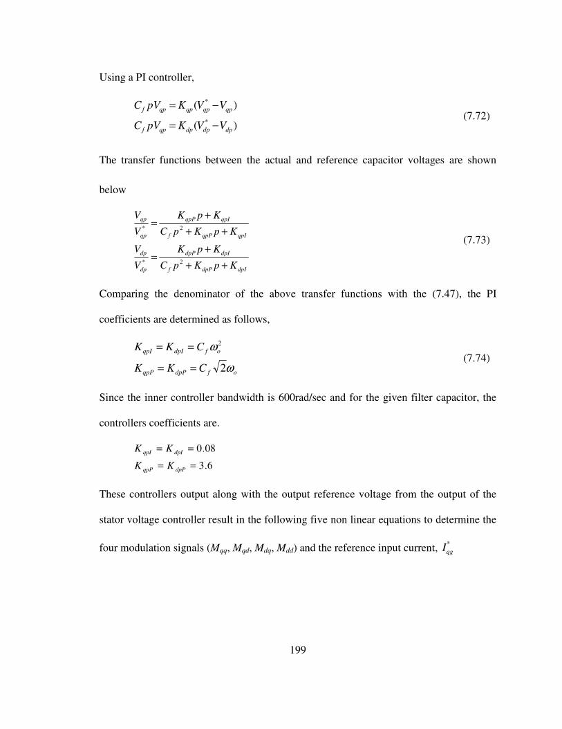
199
Using a PI controller,
)(
)(
*
*
dpdpdpqpf
qpqpqpqpf
VVKpVC
VVKpVC
−=
−= (7.72)
The transfer functions between the actual and reference capacitor voltages are shown
below
dpIdpPf
dpIdpP
dp
dp
qpIqpPf
qpIqpP
qp
qp
KpKpC
KpK
V
V
KpKpC
KpK
V
V
++
+=
++
+=
2*
2*
(7.73)
Comparing the denominator of the above transfer functions with the (7.47), the PI
coefficients are determined as follows,
ofdpPqpP
ofdpIqpI
CKK
CKK
ω
ω
2
2
==
== (7.74)
Since the inner controller bandwidth is 600rad/sec and for the given filter capacitor, the
controllers coefficients are.
6.3
08.0
==
==
dpPqpP
dpIqpI
KK
KK
These controllers output along with the output reference voltage from the output of the
stator voltage controller result in the following five non linear equations to determine the
four modulation signals (Mqq, Mqd, Mdq, Mdd) and the reference input current, *
qgI

200
*
qpV
pgV
dpV
p
KK
dpI
dpP +
p
KK
qpI
qpP +
dpσ
qpσ
dpfp VCω
qpfp VCω
*
qgI
qqM
qdM
dqM
ddM
qdsVqdsI
*
dpV
Figure 7.7 Block diagram for the input current controllers
dqqdddqq
dpddqpdqqs
dpqdqpqqqs
qpfpdsddqsqddgdp
dpfpdsdqqsqqqgqp
MMMM
VMVMV
VMVMV
VCIMIMI
VCIMIMI
=
+=
+=
+−−=
−−−=
*
*
ωσ
ωσ
(7.75)
By solving (7.75), the output of this controller together with the stator current and
voltages determines the reference q-axis source current.
))((1 **
dgqpfpdpdp
qp
dpfpqpqg IVCVPV
VCI −−+++= ωσωσ (7.76)
where
dsdsqsqs IVIVP*** += (7.77)
And finally the four modulation signals are determined using the required stator voltage
and the input capacitor voltage controller outputs as given in (7.78). The block diagram
shown in Figure 7.7 demonstrates the generation of the modulation signal.

201
Table 7.1 Control system parameters
Source voltage, Vg = 380Vrms
Input frequency, fp = 60Hz
Line resistance, Rg = 0.5Ω
Line Inductance, Lg = 1mH
Damping resistance, Rf = 30Ω
Filter Inductance, Lf = 7.46mH
Filter Capacitor, Cf = 10µF
Speed Controller
KwrP = 17
KwrI = 144
Rotor flux controller
KqrP = KdrP = 79.3
KqrI = KdrI = 3600
Inner stator current controller
KqsP = KdsP = 4.3
KqsI = KdsI = 3000
Input current controller
KqgP = KdgP = 7.2
KqgI = KdgI = 3024
Inner capacitor voltage controller
KqpP = KdpP = 0.08
KqpI = KdpI = 3.6
Induction machine parameters
Stator Resistance, Rs = 0.531Ω
Rotor Resistance, Rr = 0.408Ω
Stator Inductance, Ls = 87.22mH
Rotor Inductance, Lr = 87.22mH
Mutual Inductance, Lm = 84.7mH
Moment of Inertial, J = 0.04kg.m2
Number of pole pairs, P = 4
( )
( )
*
)(
*
)(*
*
)(
*
)(*
*
*
*
*
P
IVCVM
PV
IVCVPVM
P
IVCVM
PV
IVCVPVM
dgqpfpdpds
dd
qp
dgqpfpdpdpds
dq
dgqpfpdpqs
qd
qp
dgqpfpdpdpqs
−−−=
−−+=
−−−=
−−+=
ωσ
ωσ
ωσ
ωσ
(7.78)

202
It is possible to use (7.78) directly to model the MC fed induction motor drive system in
qd-synchronous reference frame to observe the performance of the designed controllers.
It is recommended to model the overall system without actually generating the actual
switching pulses as a first step in simulation. This is because with actual pulses, the
simulation time is significantly long. Once the controller works perfectly, the actual
switching pulses are then implemented. The time varying modulation signals which is
expressed in (3.10) are rather used to produces the switching pulses based on the
reference stator voltage and the filtered input capacitor voltage. The procedure used to
produce the actual switching signal pulses is explained in section 3.2.1.
7.2.6 Stator Flux Estimation
This section presents the rotor flux estimation which is used for the implementation
of rotor flux controller. First, the stator side flux linkages should be estimated as
accurately as possible using the Low Pass Filter (LPF) which in turn is used to determine
the rotor flux linkages. The stator flux in stationary reference frame is given as [72]:
s
qds
s
qdss
s
qds pIrV λ+= (7.79)
And from (7.79), it is possible to estimate the stator flux by integrating the back emf;
however, the pure integrator has the drift and the saturation problem by the dc offset and
initial condition.
( )∫ −= dtIrVs
qdss
s
qds
s
qdsλ (7.80)
The gain of the controllers are summarized in Table 7.1

203
The pure integrator is replaced by a LPF to solve the above problems. The estimated
stator flux by the LPF can be given as:
asVe
sl
+=
1^
λ (7.81)
where sl
^
λ is the estimated stator flux, a is the pole and Ve is the back emf shown below.
qdssqdse IrVV −= (7.82)
The phase lag and the gain created by the low pass filter are expressed in terms of the
synchronous speed, estimated flux and the pole as follows,
a
eωφ 1tan −−=
(7.83)
ee
sl
aVM
ω
λ
+==
2
^
1
(7.84)
On the contrary, the phase and gain of the pure integrator shown above is 90o and 1/ωe
respectively. Although the LPF eliminates the saturation problem and reduces the effect
of DC offsets, it brings magnitude and phase angle error due to the cut off frequency of
the LPF. This error is more severe when the machine frequency is lower than the cutoff
frequency. Therefore, the cutoff frequency is selected to be very low to mitigate this
error. However, there still remains the drift problem due to the very large time constant of
the LPF. For the exact estimation of the stator flux, the phase lag and the gain should be
the same as that of the pure integrator. Furthermore, to solve the drift problem, the pole
should be located far from the origin.

204
qdsV
qdss Ir
)/(
1
Ks eω+e
ee K
ω
ωω 22)/( +)exp( 1φj−
qdsIqdsV
)sin( 1φ
)cos( 1φ
qds
^
λ
eωeω
Figure 7.8 Bock diagram of the stator flux estimation using LPF
The decrement in the gain and the phase lag created is due to the LPF and is
compensated by multiplying a gain compensator, G and the phase compensator, P
respectively.
e
eaG
ω
ω 22 +=
(7.85)
)exp( 1φjP −= (7.86)
The new integrator along with the gain and phase compensator is
)exp(1
1
22^
φω
ωλj
a
asV e
e
e
qds−
+
+=
(7.87)
The cutoff frequency in LPF cannot be located at fixed point far from the origin.
If the pole is varied proportionally to the machine speed, the proportion of the
machine frequency to the cutoff frequency of the LPF is constant. If the proportion is
large, the estimation error will be very small. Consequently, the pole is determined to be
varied proportionally to the motor speed.

205
Therefore, the pole is located close to the origin in very low speed range and far from the
origin in high speed range. K is a constant chosen to vary the pole proportionally with the
rotor speed. Finally, the complete equation for stator flux estimator can be derived as:
Ka
eω=
)exp()/(
)/(
11
22^
φω
ωω
ω
λj
K
KsV e
ee
ee
qds−
+
+=
(7.88)
where,
)sin()cos()exp( 111 φφφ jj −=−
221
)/()cos(
ee
e
K ωω
ωφ
+=
221
)/(
/)sin(
ee
e
K
K
ωω
ωφ
+=
Simplifying (7.88) and separating into real and imaginary parts gives:
( ))(sin)(cos)/(
)/(
111
22^
dssdsqssqs
e
ee
e
qs IrVIrVK
Ks−+−
+
+= φφ
ω
ωω
ωλ (7.89)
( ))(sin)(cos)/(
)/(
111
22^
qssqsdssds
e
ee
e
ds IrVIrVK
Ks−−−
+
+= φφ
ω
ωω
ωλ (7.90)
From (7.89) and (7.90), the stator q-axis and d-axis stator fluxes are determined,
however, the control scheme proposed in this chapter requires the estimation of the rotor
fluxes. The relationships between the stator and rotor fluxes are determined as follows.
drmdssds
qrmqssqs
ILIL
ILIL
+=
+=
λ
λ (7.91)

206
Form (7.91), the rotor flux can be expressed in terms of the stator flux and currents as
given below
)(1
)(1
dssds
m
dr
qssqs
m
qr
ILL
I
ILL
I
−=
−=
λ
λ
(7.92)
Using the rotor flux equations,
drrdsmdr
qrrqsmqr
ILIL
ILIL
+=
+=
λ
λ
(7.93)
Substituting (7.92) into (7.93), the rotor flux linkages can be written in terms of stator
current and flux linkages.
)(
)(
dsds
m
rdr
qsqs
m
rqr
ILL
L
ILL
L
σ
σ
λλ
λλ
−=
−=
(7.94)
Using the estimated stator flux linkages and the measured stator currents, it is possible to
estimated the rotor flux as
)ˆ(ˆ
)ˆ(ˆ
dsds
m
rdr
qsqs
m
rqr
ILL
L
ILL
L
σ
σ
λλ
λλ
−=
−=
(7.95)
The complete block diagram of the proposed control scheme is shown in Figure 7.9. The
input unity power factor control, rotor flux estimation and the rotor filed orientation are
the basic elements of this block.

207
*
qsV
*
dsV
qsλ
dsλ abcsV
'
qpσ'
dpσ
abcsI
s
qdsV
s
qdsI
*
qrλqrσ
qs
r
mr IL
LR
drλ
1 *
soω
rω
eω
m
r
L
L
m
r
L
L
qrλ
drλ
qrλ
*
qgI
qgI
*
dpV0* =dgI
dgI qgtp ILω
dgσ
qgσ
dgtp ILω
*
qpV
pgV
dpV
dpσ
qpσ
dpfp VCω
qpfp VCω
drλ
drσ
qrsoλω
mr
r
LR
L
rω
*
rω rωσ
LTJ
P
2dsqr Iλ
drλ
1
eK
1
*
drλ
qsI
*
qsV
*
qsI
dr
r
mrqr
r
mrdse
L
L
L
LRIL λωλω σ +−
2
qsσ
*
dsI
dsI
*
dsVdsσ
qr
r
mrdr
r
mrqse
L
L
L
LRIL λωλω σ ++
2
'
qpσ
'
dpσ
qsILσ
dsILσ
eθ∫ eω
))((1 *
dgqpfpdpdp
qp
dpfp IVCVPV
VC −−++ ωσω
qpσ
pθ∫
pω
Figure 7.9 Block diagram of the proposed control scheme

208
7.3 Simulation Results and Discussions
The proposed control scheme is simulated in Matlab/Simulink platform using the
system parameters and calculated controllers gain provided in Table 1.1. The model also
includes the rotor flux estimation to provide the d-axis and q-axis rotor flux linkage to the
controllers. The matrix converter as well the induction machine models are taken from
section 5.3.1. Figure 7.10 shows the block diagram of the Simulink model. The d-axis of
the rotor flux is controlled to be constant at 0.54Wb. The command for q-axis rotor flux is
controlled to be zero which in turn assures the rotor flux orientation. The simulation has
done for three different cases as. The first simulation is done to observe the response of
the designed controllers for the load variation while keeping the speed command
constant. In the second and third simulations, the speed is ramped in both forward and
reverse direction at while the machine is under no load operation. The results of these
simulations are discussed below.
In the first simulation, a load torque of 3 Nm is applied after 1 sec while the speed
command is set to 280 rad/sec. As shown in Figure 7.11, the speed follows the reference
perfectly after the motor reaches steady state and it has very small disturbance at the time
when the load is applied. The starting transient of the electromagnetic torque is also
shown in this Figure; at steady state it follows the load torque although there is a small
overshoot at 1 sec. It can also be observed that the electromagnetic torque has very small
oscillating component. This is because the induction motor is directly fed the chopped
output voltage of the converter which is not purely sinusoidal.

209
Figure 7.10 Simulink model of the proposed control scheme
Not only the electromagnetic torque but also the stator q-axis and d-axis currents,
both components of the source current and both axes of the input capacitor voltage also
contain ripples. As seen in Figure 7.12 both q-axis and d-axis rotor flux linkages track
their respective references. From this figure, it has been observed that the d-axis rotor
flux linkage is not affected by the change in the load torque assuring the decoupled
control of flux and speed in the proposed control scheme. However, the q-axis rotor flux
linkage has small disturbance when the load applied.
The inner current controller output are shown in Figure 7.13 in which the actual and
reference are almost equal because they are in the inner control loop. Comparing Figure
7.13 and Figure 7.11, the q-axis stator current linearly changes with torque since it is a
torque producing current. And the d-axis stator current responds only for the d-axis flux
as it is a flux producing current component.

210
Figure 7.11 Speed command, actual speed and electromagnetic torque
The input d-axis current always follows the reference with small overshoot during the
transient. It also has small oscillation during the load change as seen in Figure 7.14. As a
result, the input power factor regulated at unity before and after the load applied. In this
figure, the q-axis axis input current track the current command very well after the motor
reaches steady state which proportionally increase with load. The inner voltage
controllers exactly follow the voltage command as shown in Figure 7.15. The actual
matrix converter voltage output and input are given in Figure 7.16.
The sinusoidal phase ‘a’ source current is shown in Figure 7.17 which increases with
the load. And the reactive power drawn from the source is always zero although small
amount of reactive power is absorbed during the transient and load change.
0 0.5 1 1.5274
276
278
280
282
ωr* a
nd ω
r
0 0.5 1 1.5-2
0
2
4
6
time [sec]
Te [
Nm
]

211
Figure 7.12 Estimated and reference rotor flux linkages
Figure 7.13 Actual and reference stator currents
0 0.5 1 1.50.3
0.4
0.5
0.6
λdr
* a
nd λ
dr
est [
Wb]
0 0.5 1 1.5-0.01
0
0.01
0.02
time [sec]
λqr
* a
nd λ
qr
est [W
b]
0 0.5 1 1.5-2
0
2
4
I qs
* a
nd I
qs [
A]
0 0.5 1 1.56
7
8
9
10
time [sec]
I ds
* a
nd I
ds [
A]

212
Figure 7.14 Source currents commands and actual values
Figure 7.15 Inner capacitor voltage controller’s reference and actual values
0 0.5 1 1.5-10
0
10
I qg
* a
nd I
qg [
A]
0 0.5 1 1.5-1
0
1x 10
-3
time [sec]
I dg
* a
nd I
dg [
A]
0 0.5 1 1.50
100
200
300
400
Vqp
* a
nd V
qp [
V]
0 0.5 1 1.5-5
0
5
Vdp
* a
nd V
dp [
V]
time [sec]
213
Figure 7.16 Matrix converter output and input capacitor voltage
Figure 7.17 Phase ‘a’ source current and reactive power drawn from the source
0.6 0.7 0.8 0.9 1 1.1 1.2 1.3 1.4-400
-200
0
200
400
Vas [
V]
0.6 0.7 0.8 0.9 1 1.1 1.2 1.3 1.4-400
-200
0
200
400
Vap [
V]
0.6 0.7 0.8 0.9 1 1.1 1.2 1.3
-2
0
2
I ag [
A]
time [sec]
0 0.5 1 1.5-0.2
0
0.2
time [sec]
Qin
[V
AR
]

214
Figure 7.18 Speed command, actual speed and electromagnetic torque
In the second simulation, the speed command is ramped from zero to the rated
speed in 1 sec and kept at rated speed for the rest of the time. The motor speed tracks the
reference as given in Figure 7.18. And a positive electromagnetic torque is developed
during the speed ramp and it goes back to zero after the speed becomes constant since
there is no load applied. As seen in Figure 7.19, the rotor flux linkages follows the
reference even during the ramp after the motor reaches steady state.
It can be observed from Figure 7.20, the d-axis source current is maintained zero
in both region of speed command. Since the speed is increasing linearly, the output power
also changes linearly. On the other hand, the input power only depends on the q-axis
source current as the input voltage kept constant. Therefore, Iqg should linearly vary with
the rotor speed to maintain input output power balance.
0 0.5 1 1.50
100
200
300
ωr* a
nd ω
r
0 0.5 1 1.5-10
0
10
20
time [sec]
Te [
Nm
]

215
Figure 7.19 Estimated and reference rotor flux linkages
The inner stator current and input capacitor voltage controllers which exactly
track their corresponding references are shown in Figure 7.21 and Figure 7.22
respectively. Since the voltage drop in the source current is considerably small, the q-axis
capacitor can only represent with d-axis source current and whereas the d-axis capacitor
voltage depend only on the q-axis source current. This is verified in the Figure 7.22. It
can also be seen that the input capacitor voltages have small ripple and the digital low
pass filter is implemented to remove this oscillation before they are used to generate the
modulation signals. The sinusoidal input current with amplitude vary with the rotor speed
is given in Figure 7.23. And the reactive power absorbed from the source is regulated to
zero verifying the robustness of the input power factor controller.
0 0.5 1 1.50.3
0.4
0.5
0.6
λd
r*
and λ
dr
es
t [W
b]
0 0.5 1 1.5-0.02
0
0.02
0.04
time [sec]
λq
r*
and λ
qr
es
t [W
b]

216
Figure 7.20 Source currents commands and actual values
Figure 7.21 Actual and reference stator currents
0 0.5 1 1.5-10
0
10
I qg
* a
nd I
qg [
A]
0 0.5 1 1.5-1
0
1x 10
-3
time [sec]
I dg
* a
nd I
dg [
A]
0 0.5 1 1.5
0
5
10
I qs
* a
nd I
qs [
A]
0 0.5 1 1.56
7
8
9
10
time [sec]
I ds
* a
nd I
ds [
A]

217
Figure 7.22 Inner capacitor voltage controller’s reference and actual values
Figure 7.23 Phase ‘a’ source current and reactive power drawn from the source
0 0.5 1 1.50
100
200
300
400
Vqp
* a
nd V
qp [
V]
0 0.5 1 1.5-5
0
5
Vdp
* a
nd V
dp [
V]
time [sec]
0.4 0.5 0.6 0.7 0.8 0.9 1 1.1 1.2
-5
0
5
I ag [
A]
time [sec]
0 0.5 1 1.5
-0.1
0
0.1
time [sec]
Qin
[V
AR
]

218
Figure 7.24 Speed command, actual speed and electromagnetic torque
Finally, simulation has been done to check the robustness of the control scheme
proposed in this work by using a negative ramp speed command. As seen in Figure 7.24
the speed perfectly tracks the command. Since the rotor speed command is ramped in the
reverse direction, a negative torque is developed during this time and goes back to zero
after the speed is to be set constant. As given in Figure 7.25 the rotor flux linkages
properly track their reference even if the d-axis rotor flux linkage has small negative
value during starting following the torque transient. The source currents shown in Figure
7.26 are the same as shown in Figure 7.20 regardless of the direction of rotation of the
motor. The inner stator currents and input capacitor voltage controllers perfectly follows
their reference in this scenario as well as depicted in Figure 7.27 and 7.28 respectively.
Finally, the input power factor controller works perfectly keeping the reactive power
drawn from the source to zero as shown in Figure 7.30.
0 0.5 1 1.5-400
-200
0
200
ωr* a
nd ω
r
0 0.5 1 1.5-20
-10
0
10
time [sec]
Te [
Nm
]

219
Figure 7.25 Estimated and actual rotor flux linkages
Figure 7.26 Source currents commands and measured values
0 0.5 1 1.50.3
0.4
0.5
0.6
λdr
* a
nd λ
dr
est [
Wb]
0 0.5 1 1.5-0.04
-0.02
0
0.02
time [sec]
λqr
* a
nd λ
qr
est [
Wb]
0 0.5 1 1.5-10
0
10
I qg
* a
nd I
qg [
A]
0 0.5 1 1.5-1
0
1x 10
-3
time [sec]
I dg
* a
nd I
dg [
A]

220
Figure 7.27 Actual and reference stator currents
Figure 7.28 Inner capacitor voltage controller’s reference and actual values
0 0.5 1 1.5-15
-10
-5
0
5
I qs
* a
nd I
qs [
A]
0 0.5 1 1.56
7
8
9
10
time [sec]
I ds
* a
nd I
ds [
A]
0 0.5 1 1.50
100
200
300
400
Vqp
* a
nd V
qp [
V]
0 0.5 1 1.5-5
0
5
Vdp
* a
nd V
dp [
V]
time [sec]

221
Figure 7.29 Matrix converter output and input capacitor voltage
Figure 7.30 Phase ‘a’ source current and reactive power drawn from the source
0.6 0.7 0.8 0.9 1 1.1 1.2 1.3 1.4-400
-200
0
200
400
Vas [
V]
0.6 0.7 0.8 0.9 1 1.1 1.2 1.3 1.4-400
-200
0
200
400
Vap [
V]
0.6 0.7 0.8 0.9 1 1.1 1.2 1.3
-5
0
5
I ag [
A]
time [sec]
0 0.5 1 1.5
-0.1
-0.05
0
0.05
0.1
time [sec]
Qin
[V
AR
]

222
7.4 Conclusion
A control scheme consisting of an indirect rotor field oriented control of an induction
motor fed by a direct a/ac matrix converter with unity input factor control is illustrated.
Since the studied system has non-linear dynamics, the input-output feedback linearization
technique is used to design controllers. By analyzing the stability of the zero dynamics,
the overall system is found to be input output linearizable and the designed linear
controller is implemented. Simulation results verify the robustness of the proposed
controllers for load as well as rotor speed variations.
223
CHAPTER 8
SWITCHING SIGNALS GENERATION IN NI-cRIO CHASIS
8.1 Introduction
This chapter presents the generation of switching signals using NI instruments
compact RIO on LabVIEW FPGA environment. A method used to generate these signals
is described in detail. A Matlab/SIMULINK has been done based on the actual switching
signals obtained from the FPGA to show the validity of the experimental results.
The controller used in this experiment is given in Figure 8.1. It mainly consists of
the following four main parts: NI cRIO-9022 RT controller, NI cRIO-9114 Chassis, NI
9403 digital I/O module and NI 9215 analog output modules.
NI cRIO-9114 Chassis
This reconfigurable chassis main part of the compact RION and it is capable of
accepting up to 8 compact RIO input/output modules. It has an embedded Xilinx virtex-5
reconfigurable I/O FPGA in it which provides ultimate processing power. The switching
signals generation which is described in this chapter are done directly on the embedded
FPGA using LabVIEW. Besides, this chassis contains one digital input/output and three
analog input modules.
NI 9403
NI 940 is bidirectional digital input/output module for the compact RIO chassis
which is shown in slot one of Figure 8.1.

Figure 8.1 Controller used to generate the switching signals
It contains 32 channels and each of them is compatible w
this work it is used to collect the switching signals generated by the embedded FPGA.
NI 9215
The NI 9215 module contains 4 analog inputs channels sampled in parallel with
16 bit analog-to-digital converters. The controller
shown in the last three slots in Figure 8.1.
8.2 Switching signal generation using direct digital synthesis
The modulation schemes developed in the controller is a carrier pulse modulation
which requires a generation of f
representing the desired output waveforms. Common mode voltage consists of third
224
Figure 8.1 Controller used to generate the switching signals
It contains 32 channels and each of them is compatible with 5V TTL output voltages. In
this work it is used to collect the switching signals generated by the embedded FPGA.
The NI 9215 module contains 4 analog inputs channels sampled in parallel with
digital converters. The controller contains three analog input modules as
shown in the last three slots in Figure 8.1.
Switching signal generation using direct digital synthesis
The modulation schemes developed in the controller is a carrier pulse modulation
which requires a generation of four periodic waveforms. A 30Hz three phase sinusoidal
representing the desired output waveforms. Common mode voltage consists of third
Figure 8.1 Controller used to generate the switching signals
ith 5V TTL output voltages. In
this work it is used to collect the switching signals generated by the embedded FPGA.
The NI 9215 module contains 4 analog inputs channels sampled in parallel with
contains three analog input modules as
Switching signal generation using direct digital synthesis
The modulation schemes developed in the controller is a carrier pulse modulation
our periodic waveforms. A 30Hz three phase sinusoidal
representing the desired output waveforms. Common mode voltage consists of third

225
harmonic of both input and output voltages. And a 5 kHz triangular carrier signals. To
generate these signals inside the FPGA a Direct digital synthesis (DDS) method is
implemented which provides high degrees of frequency and phase control. The core
components of a DDS waveform generator are the accumulator and lookup table.
8.2.1 Accumulator
The accumulator is a 32 bit counter which stores the current phase value of the
generated waveform. The frequency of the generated waveforms is determined by the
accumulator increment and the rate at which the accumulator is updated. Therefore, the
accumulator increment is calculated based on the desired frequency and the updated rate
as given 8.1.
frequency desired*rate Update
2Incrementr Accumulato
bitr accumulato
= (8.1)
Where update rate is the speed at which the while loop being updated and it is can be
computed using the update ticks and the FPGA clock speed as shown in (8.2). The update
ticks are defined as the number of FPGA clocks required to computer all the program
inside the loop.
ticksUpdate
(40Mz) speedClock rate Update = (8.2)
Since the program which generates the switching signals takes 900 update ticks the
frequencies are calculated as follows.

226
2, =
!"#!$∗ 900 ∗ 2(10* =
193272528
60, =201123240567895
40(10;∗ 900 ∗ 60 = 5798206
30, =201123240567895
40(10;∗ 900 ∗ 30 = 2899103
The current accumulator phase shift is used to perform a lookup operation in a
lookup table of the reference waveform to determine the next output value. When the
accumulator phase value reaches the maximum (360 degrees) it rolls over and starts again
at 0 degrees. The expression for the accumulator phase shift is given in (8.3), and it is
used to generate balanced three phase sinusoidal voltages.
shift phase desired*360
2shift phaser Accumulato
bitr accumulato
= (8.3)
1431655765120*360
2shift phaser Accumulato degree, 120For
32
==
8633115312240*360
2shift phaser Accumulato degree, 240For
32
==
8.2.2 Lookup Table
The second main component of a DDS is the lookup table which contains data of
one cycle of the waveform and typically contains 10 to 13 bits sample points which
represent the waveform to be generated. The accumulator value typically 32 bit which is
a lot more resolution than the reference waveform.

227
Figure 8.2 FPGA direct digital syntheses
The extra bits can be used for interpolation between two samples in the reference
waveform. This interpolation result in a better frequency control and less harmonic
distortion in the generated waveform. Figure 8.2 shows the FPGA DDS generator which
increments the accumulator and returns the next value for the waveform signal.

228
Figure 8.3 Ch1-SaA, Ch2-SbA and Ch3-ScA
There are two ways to determine the third switching signals from the other known
switches. One of these methods is by comparing the sum of the all the three modulation
signals with the triangular carrier. And the other way of determining it is by turning ON
when both the first two switches are OFF or OFF otherwise. Channel 3 and 4 show that it
is possible to use either of the above two methods generate the third switching signals.
The other switching signals corresponding to phase ‘b’ and phase ‘c’ output voltages are
shown in Figure 8.5 and 8.6 respectively.
SaA
SbA
ScA

229
Figure 8.4 Switching signals for phase ‘a’ output voltage
Figure 8.5 Switching signals for phase ‘b’ output voltage
SaA
SbA
ScA
SaB
SbB
ScB

230
Figure 8.6 Switching signals for phase ‘c’ output voltage
A Matlab/SIMULINK model has also been done based on the actual switching
signals obtained from the FPGA outputs. An input balanced three phase voltages of 60Hz
and 100V peak-to-peak phase voltages as seen in Figure 8.7 and desired three output
voltages of 84V peak-to-peak with 30Hz are considered. After collecting the nine
switching signals given in Figure 8.4 to Figure 8.6 and applying it on equation (8.4) and
(8.5) result in the output desired voltage. The output three phase voltages which are
shown in Figure 8.8 are 30Hz with magnitude almost equal to 84V. These prove that the
experimental results are
cpcCbpbCapaCnpcs
cpcBbpbBapaBnpbs
cpcAbpbAapaAnpas
VSVSVSVV
VSVSVSVV
VSVSVSVV
++=+
++=+
++=+
(8.4)
ScC
SbC
SaC

231
Figure 8.7 Three phase voltages at the input terminal of MC
Figure 8.8: Three phase output voltage of MC
++++
++++=
bpcCbpbCapaCbpcBbpbB
apaBbpcAbpbAapaA
npVSVSVSVSVS
VSVSVSVSV
3
1 (8.5)
0 0.01 0.02 0.03 0.04 0.05 0.06 0.07 0.08 0.09 0.1
-100
0
100
Vap [
V]
0 0.01 0.02 0.03 0.04 0.05 0.06 0.07 0.08 0.09 0.1
-100
0
100
Vbp [
V]
0 0.01 0.02 0.03 0.04 0.05 0.06 0.07 0.08 0.09 0.1
-100
0
100
Vcp [
V]
0 0.01 0.02 0.03 0.04 0.05 0.06 0.07 0.08 0.09 0.1
-80
-60
-40
-20
0
20
40
60
80

232
8.3 Conclusion
The nine switching signals which are used to generate the three phase output
voltage of a matrix converter are generated using NI instruments compact RIO. These
signals are generated using a carrier based modulation technique developed in chapter
three. Collecting the actual data from the FPGA terminals, a simulink model has been
developed to validate the generated switching pulses. Results show that the pulses
constrict a balanced desired balanced three phase voltage with specified output
frequency.

233
CHAPTER 9
CONCLUSSION AND FUTURE SUGGESTION
9.1 Summary of the Thesis
The thesis presents different modulation techniques for three phase-to-three phase
matrix converter. New approaches for determining the modulation signal are derived and
it gives the same result as the complex and the more mathematically intensive approaches
given in literature. Moreover, the actual switching pulse generations are illustrated.
Computer simulations on a Matlab/Simulink platform are done based on the analytical
modulation signals’ expressions. The results demonstrate the generation of the switching
signals which synthesize the output three phase voltages.
This work also investigates the input filter the input filter design for a three phase to
three phase matrix converter system. A new method to specify the parameters of the input
filters is set forth. The method used a harmonic balance technique to analyze the ripple
component of the input current and voltage waveforms. The filter inductor and capacitor
are determined based on the specified maximum allowable source current and input
capacitor voltage ripples under a specified damping resistance and output rated current.
Simulation results verify that the chosen resistance valued keeps the system stable.
Moreover, the rated current based designed filter parameters perfectly work for lower
output currents. Although the analysis considers only one dominant harmonic component
of the input current, the resulting filter are also capable of mitigating lower harmonics.

234
The proposed approach also maintained a high power factor at the input terminal of the
matrix converter which allows wider control range of a matrix converter. In addition, the
resonance frequency of the determined filter parameter are sufficiently lower that the
switching frequency and far from the fundamental.
A complete dynamic modeling and steady state analysis of the matrix converter
feeding an RL load is given in this thesis. This work in particular derives a new
generalized steady state analysis which enables to study the operation of the overall
system operating in various power factor operations. In addition, dynamic and steady
state analysis are developed for matrix converter fed induction motor system. In the
above both cases a computer simulation has been done to verify the theoretical analysis.
From the simulation results, it was possible to see the starting transient and the dynamic
response to a sudden change of the load during the steady state operation. Besides the
performance characteristics of the drive system has been discussed.
The thesis also present stability study of a matrix converter fed induction motor
drive system. This study is based on small signal model in synchronous reference frame.
The stability margin by examining the real values of the dominant eigen values of the
system characteristic matrix. The elements of this matrix, which are the operating points,
are evaluated through the derived approaches of steady state analysis. The work also
shows that the stability of the overall drive system is affected by different system
parameters. A lower damper resistance improves the stability of the system by drawing
high frequency components of the input current; however, this power loss in the damping
resistance becomes more significant if the resistance is too small. It is also noticed that
drive system has wider stability region while operating at a leading input power factor

235
power factor than with a lagging power factor under the specified system parameters. The
impact of the stator and rotor resistance variation on drive stability analysis is also
considered in thesis. Although the rotor and stator resistance increase due to heating
creates a challenge on the high performance induction machine control, it narrows the
instability margins. A computer simulation has been done to clearly shown stable and
unstable regions by observing the input and output voltage and current waveforms.
A high performance vector control of motor fed by a direct a/ac matrix converter with
unity input factor control is developed in this thesis. This control uses a rotor field
orientation indirect vector control by aligning the rotor flux in the synchronous reference
frame. Unlike most work presented in literature, the q-axis rotor current is controlled to
be zero. This guarantee that flux is actually oriented rather that assuming a zero. The
input-output feedback linearization technique is used as approaches to design the non
linear system. Detailed controller design is presented based on the conventional linear
controller design since the non linear system is input-output linearizable. Simulation
results verify the robustness of the proposed controllers for different load and rotor speed
variation.
Finally, the progress in the experimental results is conducted through the generation
of the actual nine firing pulses of the bidirectional switches using a carrier based
modulation technique which is relatively easier to implement as compared to the space
vector modulation. This is done on the NI instruments compact RIO on LabVIEW FPGA
environment. The validity of the generated pulses is verified by computer simulation
which is based on the actual pulses collected from the FPGA terminals. The results shows

236
that the generated firing pulses give a balanced set of output voltages with the desired
magnitude and frequency.
9.2 List of Contributions
The main contributions of the thesis are listed below
• A complete derivation of the expression of the modulation signals based on
carrier based pulse width modulation is given. This expression can be used for
both balanced and unbalanced source voltages. Since it is relatively simple, it can
suitably used for practical implementation.
• The thesis clearly present a detailed dynamic analysis for a matrix converter fed
induction motor drive system and MC feeding a linear load in synchronous
reference frame. This method uniquely represents the modulation signals in four
scalar components hence it requires less computation as compared to working on
vectors.
• Fourier representations of the switching signals of the matrix converter are
derived. And a new approach of determining the input filter parameters is
presented. The filter designed in this work not only satisfies the minimum input
power factor requirements but also it is designed to attenuate the maximum
allowable input capacitor voltage ripples.

237
• A new generalized steady state performance analysis is set forth in cases where
the matrix converter feeds induction motor as well as linear load. This modeling
can be used for both unity and non-zero reactive power at the source side. Unlike
most of the works which consider a unity input power factor to examine the
steady state operations, the analysis presented in this thesis help to study the
matrix converter based system operating in a leading and lagging input power
factors.
• A new small signal model based stability analysis is proposed for a matrix
converter fed induction motor drive system. Based on this analysis, different
factors which affect the stability of a matrix converter based drive are discussed.
This includes the effect of damping resistance in the input filter, the stator and
rotor resistances variations in the induction motor due to heating and the input
power factor.
9.3 Future Work
Most of the analytical results presented in the thesis are verified with a computer
simulation. Although the actual switching signals are generated and tested as
demonstrated in the previous chapter, it is necessary to implement on the actual converter
system. Part of the hard ware needed to conduct an experiment are already done and
described below.

Figure 9.1 Block diagram for the experimental set up
The block diagram of the experimental system consisting of the power circuit and
the control unit is given in Figure 9.1.
circuit. This commutation processes needs information about the output current direction;
therefore, it is necessary to build a sensor current with the associated FPGA
sensor interface board as seen in Figure 9.3.
realized with a nine bidirectional switches, Semicron SK60GM124 modules. The module
consists of two IGBS with common emitter connection and built in fast recovery diodes.
The power circuit as well as the gate driver board are done on PCB. External connectors
are used to interface the gate driver with the IGBTs as sown in Figure 9.2. The external
interfacing board used to connect the Compact RIO with the SPARTAN
Figure 9.4.
238
Figure 9.1 Block diagram for the experimental set up
The block diagram of the experimental system consisting of the power circuit and
ven in Figure 9.1. The SPARTAN-2E FPGA is used for commutation
circuit. This commutation processes needs information about the output current direction;
therefore, it is necessary to build a sensor current with the associated FPGA
board as seen in Figure 9.3. The power stage of the matrix converter is
realized with a nine bidirectional switches, Semicron SK60GM124 modules. The module
consists of two IGBS with common emitter connection and built in fast recovery diodes.
cuit as well as the gate driver board are done on PCB. External connectors
the gate driver with the IGBTs as sown in Figure 9.2. The external
interfacing board used to connect the Compact RIO with the SPARTAN
The block diagram of the experimental system consisting of the power circuit and
2E FPGA is used for commutation
circuit. This commutation processes needs information about the output current direction;
therefore, it is necessary to build a sensor current with the associated FPGA-current
The power stage of the matrix converter is
realized with a nine bidirectional switches, Semicron SK60GM124 modules. The module
consists of two IGBS with common emitter connection and built in fast recovery diodes.
cuit as well as the gate driver board are done on PCB. External connectors
the gate driver with the IGBTs as sown in Figure 9.2. The external
interfacing board used to connect the Compact RIO with the SPARTAN-2E is shown in

239
Figure 9.2 Laboratory prototype 3x3 matrix converter
Figure 9.3 Current sensor-FPGA interface board

240
Figure 9.4 Compact cRio-FPGA interfacing board

241
REFERENCES
242
[1] L. Gyugyi and B. R. Pelly, Static Power Frequency Changers: Theory, Performance
and Application, John Wiley & Sons, New York, 1976.
[2] Alesina and M. Venturini, “Solid-state Power Conversion: A Fourier Analysis
Approach to Generalized Transformer Synthesis,” IEEE Transactions On Circuits
and System, vol. CAS-28, pp. 319–330, Apr. 1981.
[3] A. Alesina and M. Venturini, “Analysis and Design of Optimum Amplitude Nine-
switch Direct AC-AC Converters,” IEEE Transactions on Power Electronics, vol. 4,
no. 1, pp. 101-112, Jan. 1989.
[4] G. Holmes and T. A. Lipo, “Implementation of a Controlled Rectifier Using AC-AC
Matrix Converter Theory,” IEEE Transactions on Power Electronics, vol. 7, no. 1,
pp. 240-250, Jan. 1992.
[5] G. Holmes, “Unified Modulation Algorithm for Voltage and Current Source Inverters
based on AC-AC Matrix Converter Theory,” IEEE Transactions on Industry
Applications, vol. 28, no. 1, pp. 31-40, Jan/Feb 1992.
[6] D. L. Huber and D. Borojevic, “Space Vector Modulated Three-phase to Three-phase
Matrix Converter with Input power Factor Correction,” IEEE Transactions on Power
Electronics, vol. 31, no. 6, pp. 1234-1246, Nov./Dec. 1995.
[7] D. Casadei, G. Serra and A. Tani, “Reduction of the Input Current Harmonic Content
in Matrix Converters under Input/output Unbalance,” IEEE Transactions on
Industrial Electronics, vol. 5, no. 3, pp. 401-411, Jun 1998.
[8] P. W. Wheeler, J. Rodriguez, J. C. Clare, L. Empringham and A. Weinstein, “Matrix
Converters: A Technology Review,” IEEE Transactions on Industrial Electronics,
vol. 49, no. 2, pp. 276-288, Apr. 2002.
[9] C. Klumpner, P. Nielsen, I. Boldea and F. Blaabjerg, “A new matrix converter motor
(MCM) for industry applications,” IEEE Transactions on Industrial Electronics, vol.
49, no. 2, pp. 325-335, Apr. 2002.

243
[10] J. Clare and P. Wheeler, “New Technology: Matrix converters”, IEEE IES
Newsletter, vol. 52, no. 1, pp. 10-12, Mar. 2005.
[11] P. W. Wheeler, J.C. Clare, L. Empringham, M. Apap and M. Bland, “Matrix
Converters”, IEEE Power Eng., Journal, vol. 16, no. 6, pp. 273- 282, Dec. 2002.
[12] P. W. Wheeler, P. Zanchetta, J. C. Clare, L. Empringham, M. Bland and D. Katsis,
“A Utility Power Supply Based on a Four-Output Leg Matrix Converter,” IEEE
Transactions on Industry Applications, vol. 44, no. 1, pp. 174-186, Jan.-Feb. 2008.
[13] P. W. Wheeler, P. Zanchetta, J. C. Clare, L. Empringham, M. Bland and D. Katsis,
“Control Design of a Three-Phase Matrix-Converter-Based AC–AC Mobile Utility
Power Supply,” IEEE Transactions on Industrial Electronics, vol. 55, no.1, pp. 209-
217, Jan. 2008.
[14] R. Vargas, J. Rodriguez, U. Ammann, P. W. Wheeler, “Predictive Current Control of
an Induction Machine Fed by a Matrix Converter With Reactive Power Control,”
IEEE Transactions on Industrial Electronics, vol. 55, no. 12, pp. 4362-4371, Dec.
2008
[15] P. W. Wheeler, J. C. Clare, M. Apap and K. J Bradley, “Harmonic Loss Due to
Operation of Induction Machines From Matrix Converters,” IEEE Transactions on
Industrial Electronics, vol. 55, no. 2, pp. 809-816, Feb. 2008.
[16] A. Arias, L. Empringham, G. M. Asher, P. M. Wheeler, M. Bland, M. Apap, M.
Sumner and J. C. Clare, “Elimination of Waveform Distortions in Matrix Converters
Using a New Dual Compensation Method,” IEEE Transactions on Industrial
Electronics, vol. 54, no. 4, pp. 2079-2087, Aug. 2007.
[17] S. L. Arevalo, P. Zanchetta, P. W. Wheeler, A. Trentin and L. Empringham, “Control
and Implementation of a Matrix-Converter-Based AC Ground Power-Supply Unit for
Aircraft Servicing,” IEEE Transactions on Industrial Electronics, vol. 57, no. 6, pp.
2076-2084, June 2010.

244
[18] P. W. Wheeler, J.C. Clare and L. Empringham, “A Vector Controlled MCT Matrix
Converter Induction Motor Drive with Minimized Commutation Times and Enhanced
Waveform Quality,” in proc. IAS’02, vol. 1, no., pp. 466- 472, 2002.
[19] D. Casadei, G. Serra and A. Tani, “The Use of Matrix Converters in Direct Torque
Control of Induction Machines,” IEEE Transactions on Industrial Electronics, vol.
48, no. 6, pp. 1057-1064, Dec 2001.
[20] R. W. Bucknall and K. M. Ciaramella, “On the Conceptual Design and Performance
of a Matrix Converter for Marine Electric Propulsion,” IEEE Transactions on Power
Electronics, vol. 25, no. 6, pp. 1497-1508, June 2010.
[21] L. Zarri, M. Mengoni and O. Ojo, “Improvement in the Control Range of Matrix
Converter,” in proc. IEEE ECCE’11, Phoenix, AZ, Sept. 2011.
[22] Y. Shi, X. Yang, Q. He and Z. Wang, “Research on a novel capacitor clamped
multilevel matrix converter,” IEEE Transactions on Power Electronics, vol. 20, no. 5,
pp. 1055- 1065, Sept. 2005.
[23] P. C. Loh; R. Rong; F. Blaabjerg and P. Wang, “Digital Carrier Modulation and
Sampling Issues of Matrix Converters,” IEEE Transactions on Power Electronics,
vol. 24, no. 7, pp. 1690-1700, July 2009.
[24] P. Nielsen, F. Blaabjerg and J. K. Pedersen, “New protection issues of a matrix
converter: design considerations for adjustable-speed drives,” IEEE Transactions on
Industry Applications, vol. 35, no. 5, pp. 1150-1161, Sep/Oct 1999.
[25] J. W. Kolar, F. Schafmeister, S. D. Round and H. Ertl, “Novel Three-Phase AC–AC
Sparse Matrix Converters,” IEEE Transactions on Power Electronics, vol. 22, no. 5,
pp. 1649-1661, Sept. 2007.
[26] D. Casadei, G. Serra, A. Tani and L. Zarri, “Matrix converter Modulation Strategies:
A New General Approach Based on Space Vector Representation of the Switch
State,” IEEE Transactions on Industrial Electronics, vol. 49, no. 2, pp. 370-381, Apr.
2002.

245
[27] A. G. H. Accioly, F. Bradaschia, M. C. Cavalcanti, F. A. S. Neves and V. N. Lima,
“Generalized Modulation Strategy for Matrix Converters - Part I,” IEEE Transactions
on Industrial Electronics, vol. 56, no. 2, pp. 326-336, Feb. 2009.
[28] F. Bradaschia, M. C. Cavalcanti, F. A. S. Neves, V. N. Lima and A. G. H. Accioly,
“Generalized Modulation Strategy for Matrix Converters - Part II”, in proc. on IEEE
PESC’ 07, pp.665-671, 17-21 June 2007.
[29] L. Helle, K. B Larsen, A. H. Jorgensen, S. Munk-Nielsen and F. Blaabjerg,
“Evaluation of modulation schemes for three-phase to three-phase matrix converters,”
IEEE Transactions on Industrial Electronics, vol. 51, no.1, pp. 158- 171, Feb. 2004.
[30] F. Gao and M. R. Iravani, “Dynamic Model of a Space Vector Modulated Matrix
Converter,” IEEE Transactions on Power Delivery, vol. 22, no.3, pp. 1696-1705, July
2007.
[31] H. M. Nguyen, H. Lee and T. Chun, “Input Power Factor Compensation Algorithms
Using a New Direct-SVM Method for Matrix Converter” IEEE Transactions on
Industrial Electronics, vol. 58, no. 1, pp. 232-243, Jan. 2011.
[32] D. Casadei, G. Serra, A. Tani and L. Zarri, “Optimal Use of Zero Vectors for
Minimizing the Output Current Distortion in Matrix Converters” IEEE Transactions
on Industrial Electronics, vol. 56, no. 2, pp. 326-336, Feb. 2009.
[33] M. Mihret, M. Abreham, O. Ojo and S. Karugaba, “Modulation Schemes for Five-
Phase to Three-phase AC-AC Matrix Converters,” in proc. IEEE ECCE’10, Atlanta,
GA, 2010, pp. 1887-1893.
[34] S. Ahmed, A. Iqbal, H. Abu-Rub, J. Rodriguez, C. Rojas and M. Saleh, “Simple
Carrier Based PWM Technique for a Three-to-Nine Phase Direct AC-AC Converter,”
IEEE Transactions on Industrial Electronics, , vol. 58, no. 11, pp. 5014-5023, Nov.
2011.
[35] J. W. Kolar, F. Schafmeister, S. D. Round and H. Ertl, “Novel Three-Phase AC–AC
Sparse Matrix Converters,” IEEE Transactions on Power Electronics, vol. 22, no. 5,
pp. 1649-1661, Sept. 2007.

246
[36] S. Ahmed, A. Iqbal, H. Abu-Rub, “Generalized Duty-Ratio-Based Pulse Width
Modulation Technique for a Three-to-k Phase Matrix Converter,” IEEE Transactions
on Industrial Electronics, vol. 58, no. 9, pp. 3925-3937, Sept. 2011.
[37] H. Hojabri, H. Mokhtari and L. Chang, “A Generalized Technique of Modeling,
Analysis, and Control of a Matrix Converter Using SVD,” IEEE Transactions on
Industrial Electronics, vol. 58, no. 3, pp. 949-959, Mar 2011.
[38] A. Iqbal, E. Levi, M. Jones, S. N. Vukosavic, “Generalised Sinusoidal PWM with
Harmonic Injection for Multi-Phase VSIs,” in proc. on IEEE PESC '06. pp. 1-7, 18-
22 June 2006.
[39] A. Iqbal, E. Levi, M. Jones, S. N. Vukosavic, “Generalised Sinusoidal PWM with
Harmonic Injection for Multi-Phase VSIs,” in proc. on IEEE PESC '06. pp. 1-7, 18-
22 June 2006.
[40] D. Casadei, G. Serra, A. Tani and L. Zarri, “Effects of input voltage measurement on
stability of matrix converter drive system,” IEE Proceedings on Electric Power
Applications, vol. 151, no. 4, pp. 487- 497, 7 July 2004.
[41] R. Cardenas, R. Pena, G. Tobar, J. Clare, P. Wheeler and G. Asher, “Stability
Analysis of a Wind Energy Conversion System Based on a Doubly Fed Induction
Generator Fed by a Matrix Converter,” IEEE Transactions on Industrial Electronics,
vol. 56, no. 10, pp. 4194-4206, Oct. 2009.
[42] F. Liu, C. Klumpner and F. Blaabjerg, “Stability analysis and experimental evaluation
of a matrix converter drive system,” in proc. on IEEE IECON '03., vol. 3, pp. 2059-
2065, Nov. 2003.
[43] F. Liu, C. Klumpner and F. Blaabjerg, “A robust method to improve stability in
matrix converters,” in proc. on. IEEE PESC, vol. 5, pp. 3560- 3566, June 2004.
[44] D. Casadei, J. Clare, L. Empringham, G. Serra, A. Tani, A. Trintin, P. Wheeler and L.
Zarri, “Large signal model for the stability analysis of matrix converters,” IEEE
Transactions on Industrial Electronics, vol. 54, no. 2, pp. 939-950, Apr. 2007.

247
[45] M. Mihret, and O. Ojo, “Modeling and analysis of an AC-AC matrix converter
feeding an induction motor,” in proc. IEEE APEC’11, Fortworth, TX, 2011, pp.
1902-1909.
[46] K. Lee and F. Blaabjerg, “Simple Power Control for Sensorless Induction Motor
Drives Fed by a Matrix Converter,” IEEE Transactions on Energy Conversion, vol.
23, no. 3, pp. 781-788, Sept 2008.
[47] J. I. Sato, A. Odaka, H. Ohguchi, H. Kodachi and N. Eguchi, “A novel approach to
practical matrix converter motor drive system with reverse blocking IGBT,” IEEE
Transactions on Power Electronics, vol. 20, no. 6, pp. 1356- 1363, Nov. 2005.
[48] P. W. Wheeler, H. Zhang, D. A. Grant, “A theoretical and practical consideration of
optimised input filter design for a low loss matrix converter,” in proc. on Fifth
International Conference on Power Electronics and Variable-Speed Drives, vol., no.,
pp. 363-367, Oct 1994.
[49] V. Vlatkovic, D. Borojevic and F. C. Lee, “Input filter design for power factor
correction circuits,” , IEEE Transactions on Power Electronics, vol. 11, no. 1, pp.
199-205, Jan 1996.
[50] D. Casadei, P. Nielsen, G. Serra and A. Tani, “Theoretical and Experimental Analysis
of SVM-Controlled Matrix” Trans. on ELECTOMOTION, no. 4, pp. 28-37, 1997.
[51] H. She, H, Lin, X. Wang and L. Yue, “Damped input filter design of matrix
converter,” Power Electronics and Drive Systems, 2009. PEDS 2009. International
Conference on, pp.672-677, 2-5 Nov. 2009.
[52] T. F. Podlesak and D. Katsis, “A 150 kVA vector controlled matrix converter
induction motor drive,” Industry Applications Conference, 39th IAS Annual Meeting.
Conference Record of the 2004 IEEE, vol. 3, pp. 1811- 1816, Oct. 2004.
[53] S. Bernet, Ponnaluri and R. Teichmann, “Design and loss comparison of matrix
converters, and voltage-source converters for modern AC drives,” IEEE Transactions
on Industrial Electronics, vol. 49, no. 2, pp. 304-314, Apr 2002.

248
[54] T. Kume, K. Yamada, T. Higuchi, E. Yamamoto, H. Hara, T. Sawa and M. M
Swamy, “Integrated Filters and Their Combined Effects in Matrix Converter,” IEEE
Transactions on Industry Applications, vol. 43, no. 2, pp. 571-581, Mar.-Apr. 2007.
[55] I. Deslauriers, N. Avdiu, B. K. Ooi, “Naturally sampled triangle carrier PWM
bandwidth limit and output spectrum,” in proc. on IECON’02 , vol. 1, pp. 1- 5, Nov.
2002.
[56] M. Odavic, M. Sumner, P. Zanchetta and J. C. Clare, “A Theoretical Analysis of the
Harmonic Content of PWM Waveforms for Multiple-Frequency Modulators,” IEEE
Transactions on Power Electronics, vol. 25, no. 1, pp. 131-141, Jan. 2010.
[57] N. R. Zargari, G. Joos and P. D. Ziogas, “Input filter design for PWM current-source
rectifiers,” IEEE Transactions on Industry Applications, vol. 30, no. 6, pp. 1573,
Nov/Dec 1994.
[58] D. G. Holmes and T. A. Lipo, Pulse Width Modulation for Power Converters, New
York: Wiley, 2003.
[59] P. Wood, Switching Power Converters, Robert E. Krieger publishing company, inc,
Florida, 1984.
[60] R. Stengel, Stochastic Optimal Control, Wiley, New York.
[61] G. N. Watson, Theory of Bessel Functions, Cambridge, U.K., Cambridge Univ. Press,
1944.
[62] S. Karugaba, “Dynamics and Control of a Five Phase Induction Machine,” PhD
Dissertation, Tennessee Technological University, 2008.
[63] G. Dong, “Sensorless and Efficiency Optimazed Induction Machine Control with
Associated Converter PWM Modulation Scheme,” PhD Dissertation, Tennessee
Technological University, 2005.
[64] J. Thongam, “High Performance Sensorless Induction Motor Drive,” PhD
Dissertation, University of Quebec at Chicoutimi, 2006.

249
[65] Z. Wu, “An Investigation of Dual Stator Winding Induction Machines,” PhD
Dissertation, Tennessee Technological University, 2006.
[66] K. Lee and F. Blaabjerg, “Improved sensorless vector control for induction motor
drives fed by a matrix converter using nonlinear modeling and disturbance observer,”
IEEE Transactions on Energy Conversion, vol. 21, no. 1, pp. 52- 59, March 2006.
[67] L. Zarri, “Control of Matrix Converter,” PhD Dissertation, University of Bologna,
2007.
[68] K. Lee, F. Blaabjerg, “Sensorless DTC-SVM for Induction Motor Driven by a Matrix
Converter Using a Parameter Estimation Strategy,” IEEE Transactions on Industrial
Electronic, vol. 55, no. 2, pp. 512-521, Feb. 2008.
[69] K. Lee and F. Blaabjerg, “Simple Power Control for Sensorless Induction Motor
Drives Fed by a Matrix Converter,” IEEE Transactions on Energy Conversion, vol.
23, no. 3, pp. 781-788, Sept. 2008.
[70] O. Ojo, Z. Wu, G. Dong and S. K. Asuri, “High-performance speed-sensorless control
of an induction motor drive using a minimalist single-phase PWM converter,” IEEE
Transactions on Industry Applications, vol. 41, no. 4, pp. 996- 1004, July-Aug. 2005.
[71] L. Ben-Brahim and A. Kawamura, “A fully digitized field-oriented controlled
induction motor drive using only current sensors,” IEEE Transactions on Power
Electronics , vol. 39, pp. 241–249, June 1992.
[72] M. Shin; D. Hyun, S. Cho and S. Choe, “An improved stator flux estimation for speed
sensorless stator flux orientation control of induction motors,” IEEE Transactions on
Power Electronics, vol. 15, no.2, pp. 312-318, Mar 2000.
[73] J. E. Slotine and W. Li, Applied Nonlinear Control, Prentice Hall, 1998.
[74] B. Karanayil, M. F. Rahman and C. Grantham , “Online Stator and Rotor Resistance
Estimation Scheme Using Artificial Neural Networks for Vector Controlled Speed
Sensorless Induction Motor Drive,” IEEE Transactions on Industrial Electronics, vol.
54, no. 1, pp. 167-176, Feb. 2007.

250
[75] J. Rodriguez, M. Rivera, J. W. Kolar and P. W. Wheeler, “A Review of Control and
Modulation Methods for Matrix Converters,” IEEE Transactions on Industrial
Electronics, vol. 59, no.1, pp. 58-70, Jan. 2012.
[76] P. Kulkarni, M. T. Abraham and S. P. Das, “Design and simulation of a matrix
converter-fed scalar controlled of synchronous motor drive,” in proc. on IEEE
INDICON 2008, vol. 1, pp. 69-74, 11-13 Dec. 2008.
[77] Peter Vas, Sensorless Vector and Direct Torque Control, Oxford University Press,
1998.
[78] M.H. Rashid, Power Electronics: Circuits, Devices, and Applications, 2nd Edition,
Prentice Hall, 1993.
[79] D. Casadei, G. Serra, A. Tani and L. Zarri, “Effect of the Switching Strategy on the
Input Power Quality of Matrix Converter,” in proc. on IEEE Bologna PowerTech
Conference, vol.1, pp 23-26, June 2003.
[80] D. Xiao, “Improvement in Sensorless Direct Torque Control for Matrix Converter
Driven Interiour Permanent Magnet Synchronous Machine,” PhD Dissertation,
School of Electrical Engineering and Telecommunication, 2010.
[81] H. D. Black and W. B. Dockrell, Modulation Theory, SCRE publication, 1984.
[82] E. Ibarra, I. Kortabarria, J. Andreu, I. M. Alegria, J. L. Martin and P. Ibanez,
“Improvement of the Design Process of Matrix Converter Platforms Using the
Switching State Matrix Averaging Simulation Method,” IEEE Transactions on
Industrial Electronics, vol. 59, no. 1, pp. 220-234, Jan. 2012.
[83] X. Wang, H. Lin, H. She and B. Feng, “A Research on Space Vector Modulation
Strategy for Matrix Converter Under Abnormal Input-Voltage Conditions,” IEEE
Transactions on Industrial Electronics, vol. 59, no. 1, pp. 93-104, Jan. 2012.
[84] P. Kiatsookkanatorn and S. Sangwongwanich, “A Unified PWM Method for Matrix
Converters and Its Carrier-Based Realization Using Dipolar Modulation Technique,”
IEEE Transactions on Industrial Electronics, vol. 59, no. 1, pp. 80-92, Jan. 2012.

251
[85] A. Dasgupta and P. Sensarma, “An Integrated Filter and Controlled Design for Direct
Matrix Converter,” in proc. IEEE ECCE’11, Phoenix, AZ, Sept. 2011.

252
APPENDIX

253
APPENDIX A
COMPLETE DERIVATION OF OUTPUT VOLTAGE SPACE
VECTORS
This section gives the detailed derivation of the output voltage space vector used
in the direct space vector modulation. The calculated magnitude and angle of the output
voltage space vectors are used to construct Table 3.1
• Mode AAA
When Sap = Sbp = Scp = 0 implies Vas = Vbs = Vcs = Vap
The q-axis and d-axis output voltage space vector are determined as below.
02
1
2
1
3
2
2
1
2
1
3
2=
−−=
−−= apapapcsbsasqs VVVVVVV (A.1)
( ) ( ) 03
1
3
1=−=−= apapbscsds VVVVV (A.2)
The magnitude and direction of the output voltage space vector respectively are
calculated using (A.1) and (A.2) as follows.
022
=+= dsqsp VVV (A.3)
0tan 1 =
−= −
qs
dss
V
Vα (A.4)

254
• Mode AAB
The q-axis and d-axis output voltage space vector are determined as below.
abpbpapapcsbsasqs VVVVVVVV3
1
2
1
2
1
3
2
2
1
2
1
3
2=
−−=
−−=
(A.5)
( ) ( )abpapbpbscsds VVVVVV
3
1
3
1
3
1−=−=−= (A.6)
The magnitude and direction of the output voltage space vector respectively are
calculated using (A.5) and (A.6) as follows.
abpababdsqsp VVVVVV3
2
3
1
3
122
22=
−+
=+= (A.7)
( )3
3tan
3
1
3
1
tantan 111 πα ==
=
−= −−−
abp
abp
qs
dss
V
V
V
V (A.8)
• Mode AAC
When Sap = Sbp = 0 and Scp = 1 implies Vas = Vbs = Vap and Vcs = Vcp
The q-axis and d-axis output voltage space vector are determined as below.
capcpapapcsbsasqs VVVVVVVV
3
1
2
1
2
1
3
2
2
1
2
1
3
2−=
−−=
−−= (A.9)
( ) ( )capapcpbscsds VVVVVV
3
1
3
1
3
1=−=−= (A.10)
The magnitude and direction of the output voltage space vector respectively are
calculated using (A.9) and (A.10) as follows.

255
capcapcapdsqss VVVVVV3
2
3
1
3
122
22=
+
−=+= (A.11)
3
2
3
1
3
1
tantan 11 πα −=
−
−
=
−= −−
cap
cap
qs
dss
V
V
V
V (A.12)
• Mode ABA
When Sap = Scp = 0 and Sbp = 1 implies Vas = Vcs = Vap and Vbs = Vap
The q-axis and d-axis output voltage space vector are determined as below.
abpapbpapcsbsasqs VVVVVVVV3
1
2
1
2
1
3
2
2
1
2
1
3
2=
−−=
−−= (A.13)
( ) ( )abpbpapbscsds VVVVVV
3
1
3
1
3
1=−=−= (A.14)
The magnitude and direction of the outputs voltage space vector respectively are
calculated using (A.13) and (A.14) as follows.
abpababdsqss VVVVVV3
2
3
1
3
122
22=
+
=+= (A.15)
3
3
1
3
1
tantan 11 πα −=
−
=
−= −−
abp
abp
qs
dss
V
V
V
V (A.16)
• Mode ABB
When Sap = 0 and Sbp = Scp = 1 implies Vas = Vap and Vbs = Vcs = Vbp
The q-axis and d-axis output voltage space vector are determined as below.

256
abpbpbpapcsbsasqs VVVVVVVV3
2
2
1
2
1
3
2
2
1
2
1
3
2=
−−=
−−= (A.17)
( ) ( ) 03
1
3
1=−=−= bpbpbscsds VVVVV (A.18)
The magnitude and direction of the outputs voltage space vector respectively are
calculated using (A.17) and (A.18) as follows.
abpabdsqss VVVVV3
2
3
22
22=
=+= (A.19)
0
3
1
0tantan 11 =
=
−= −−
abpqs
dss
VV
Vα (A.20)
• Mode ABC
When Sap = 0, Sbp = 1 and Scp = 2 implies Vas = Vap, Vbs = Vbp and Vcs = Vcp
The q-axis and d-axis output voltage space vector are determined as below.
apcpbpapcsbsasqs VVVVVVVV =
−−=
−−=
2
1
2
1
3
2
2
1
2
1
3
2
(A.21)
( ) ( ) bcpbpcpbscsds VVVVVV3
1
3
1
3
1−=−=−= (A.22)
The line-to-line voltage can be expressed as:
)3
2sin(3
πω += tVV ppab (A.23)
)sin(3 tVV ppbc ω= (A.24)
)3
2sin(3
πω −= tVV ppca (A.25)

257
The magnitude and direction of the outputs voltage space vector respectively are
calculated using (A.21) to (A.25) as follows.
pbcpapdsqss VVVVVV =+=+= 2222
3
1 (A.26)
ttV
tV
V
Vp
pp
pp
qs
dss ω
ω
ω
α =
=
−= −−
)cos(
)sin(33
1
tantan 11 (A.27)
• Mode ACA
When Sap = Scp = 0 and Sbp = 2 implies Vas = Vcs = Vap and Vbs = Vcp
The q-axis and d-axis output voltage space vector are determined as below.
capapcpapcsbsasqs VVVVVVVV
3
1
2
1
2
1
3
2
2
1
2
1
3
2−=
−−=
−−= (A.28)
( ) ( )capcpapbscsds VVVVVV
3
1
3
1
3
1−=−=−= (A.29)
The magnitude and direction of the output voltage space vector respectively are
calculated using (A.28) and (A.29) as follows.
capcapcapdsqss VVVVVV3
2
3
1
3
122
22=
−+
−=+= A.30)
3
2
3
1
3
1
tantan 11 πα −=
−
=
−= −−
cap
cap
qs
dss
V
V
V
V (A.31)

258
• Mode ACB
When Sap = 0, Sbp = 2 and Scp = 1 implies Vas = Vap, Vbs = Vcp and Vcs = Vbp
The q-axis and d-axis output voltage space vector are determined as below.
apcpbpapcsbsasqs VVVVVVVV =
−−=
−−=
2
1
2
1
3
2
2
1
2
1
3
2 (A.32)
( ) ( ) bcpbpcpbscsds VVVVVV3
1
3
1
3
1=−=−= (A.33)
The magnitude and direction of the output voltage space vector respectively are
calculated using (A.32) and (A.33) as follows.
pbcpapdsqss VVVVVV =+=+= 2222
3
1 (A.32)
ttV
tV
V
Vp
pp
pp
qs
dss ω
ω
ω
α −=
−
=
−= −−
)cos(
)sin(33
1
tantan 11 (A.33)
• Mode ACC
When Sap = 0, Sbp = 2 and Scp = 2 implies Vas = Vap, Vbs = Vcp and Vcs = Vcp
The q-axis and d-axis output voltage space vector are determined as below.
capcpcpapcsbsasqs VVVVVVVV
3
2
2
1
2
1
3
2
2
1
2
1
3
2−=
−−=
−−= (A.34)
( ) ( ) 03
1
3
1=−=−= cpcpbscsds VVVVV (A.35)
The magnitude and direction of the output voltage space vector respectively are
calculated using (A.34) and (A.35) as follows.

259
capcapdsqss VVVVV3
2
3
22
22=
−=+= (A.36)
πα =
−
=
−= −−
capqs
dss
VV
V
3
1
0tantan 11
(A.37)
• Mode BAA
When Sap = 1, Sbp = 0 and Scp = 0 implies Vas = Vbp, Vbs = Vap and Vcs = Vap
The q-axis and d-axis output voltage space vector are determined as below.
abpapapbpcsbsasqs VVVVVVVV3
2
2
1
2
1
3
2
2
1
2
1
3
2−=
−−=
−−= (A.38)
( ) ( ) 03
1
3
1=−=−= apapbscsds VVVVV (A.39)
The magnitude and direction of the output voltage space vector respectively are
calculated using (A.38) and (A.29) as follows.
abpabdsqss VVVVV3
2
3
22
22=
−=+= (A.40)
πα =
−
=
−= −−
abpqs
dss
VV
V
3
2
0tantan 11
(A.41)
• Mode BAB
When Sap = 1, Sbp = 0 and Scp = 1 implies Vas = Vbp, Vbs = Vap and Vcs = Vbp
The q-axis and d-axis output voltage space vector are determined as below.

260
abpbpapbpcsbsasqs VVVVVVVV
3
1
2
1
2
1
3
2
2
1
2
1
3
2−=
−−=
−−= (A.42)
( ) ( )abpapbpbscsds VVVVVV
3
1
3
1
3
1−=−=−= (A.43)
The magnitude and direction of the output voltage space vector respectively are
calculated using (A.42) and (A.43) as follows.
abpababdsqss VVVVVV3
2
3
1
3
122
22=
−+
−=+= (A.44)
3
2
3
13
1
tantan 11 πα =
−
=
−= −−
abp
abp
qs
dss
V
V
V
V (A.45)
• Mode BAC
The q-axis and d-axis output voltage space vector are determined as below.
bpcpapbpcsbsasqs VVVVVVVV =
−−=
−−=
2
1
2
1
3
2
2
1
2
1
3
2 (A.46)
( ) ( )capapcpbscsds VVVVVV
3
1
3
1
3
1=−=−= (A.47)
The magnitude and direction of the output voltage space vector respectively are
calculated using (A.46) and (A.47) as follows.
pcapbpdsqss VVVVVV =+=+= 2222
3
1 (A.46)
261
3
2
)3
2cos(
)3
2sin(3
3
1
tantan 11 πω
πω
πω
α +−=
−
−−
=
−= −−
t
tV
tV
V
Vp
pp
pp
qs
dss (A.47)
• Mode BBA
The q-axis and d-axis output voltage space vector are determined as below.
abpapbpbpcsbsasqs VVVVVVVV3
1
2
1
2
1
3
2
2
1
2
1
3
2−=
−−=
−−= (A.48)
( ) ( )abpbpapbscsds VVVVVV
3
1
3
1
3
1=−=−= (A.49)
The magnitude and direction of the output voltage space vector respectively are
calculated using (A.48) and (A.49) as follows.
abpababdsqss VVVVVV3
2
3
1
3
122
22=
+
−=+= (A.50)
3
2
3
13
1
tantan 11 πα −=
−
−
=
= −−
abp
abp
qs
dss
V
V
V
V (A.51)
• Mode BBB
The q-axis and d-axis output voltage space vector are determined as below.
02
1
2
1
3
2
2
1
2
1
3
2=
−−=
−−= bpbpbpcsbsasqs VVVVVVV (A.52)
( ) ( ) 03
1
3
1=−=−= bpbpbscsds VVVVV (A.53)

262
The magnitude and direction of the output voltage space vector respectively are
calculated using (A.52) and (A.53) as follows.
022
=+= dsqss VVV (A.54)
0tan 1 =
= −
qs
dss
V
Vα (A.55)
• Mode BBC
The q-axis and d-axis output voltage space vector are determined as below.
bcpcpbpbpcsbsasqs VVVVVVVV3
1
2
1
2
1
3
2
2
1
2
1
3
2=
−−=
−−=
(A.56)
( ) ( )bcpbpcpbscsds VVVVVV
3
1
3
1
3
1−=−=−= (A.57)
The magnitude and direction of the output voltage space vector respectively are
calculated using (A.56) and (A.57) as follows.
bcpbcpbcpdsqsp VVVVVV3
2
3
1
3
122
22=
−+
=+= (A.58)
3
3
13
1
tantan 11 πα =
=
−= −−
bcp
bcp
qs
dsv
V
V
V
V (A.59)
• Mode BCA
The q-axis and d-axis output voltage space vector are determined as below.
bpcpapbpcsbsasqs VVVVVVVV =
−−=
−−=
2
1
2
1
3
2
2
1
2
1
3
2 (A.60)

263
( ) ( ) capcpapbscsds VVVVVV3
1
3
1
3
1−=−=−= (A.61)
The magnitude and direction of the output voltage space vector respectively are
calculated using (A.60) and (A.61) as follows.
pcapbpdsqss VVVVVV =+=+= 2222
3
1 (A.62)
3
2
)3
2cos(
)3
2sin(3
3
1
tantan 11 πω
πω
πω
α −=
−
−
=
−= −− t
tV
tV
V
Vp
pp
pp
qs
dss (A.63)
• Mode BCB
The q-axis and d-axis output voltage space vector are determined as below.
bcpbpcpbpcsbsasqs VVVVVVVV3
1
2
1
2
1
3
2
2
1
2
1
3
2=
−−=
−−= (A.64)
( ) ( )bcpcpbpbscsds VVVVVV
3
1
3
1
3
1=−=−= (A.65)
The magnitude and direction of the output voltage space vector respectively are
calculated using (A.64) and (A.65) as follows.
bcpbcpbcpdsqss VVVVVV3
2
3
1
3
122
22=
+
=+= (A.66)
3
3
1
3
1
tantan11 π
α −=
−
=
= −−
bcp
bcp
qs
dss
V
V
V
V (A.67)

264
• Mode BCC
The q-axis and d-axis output voltage space vector are determined as below.
bcpcpcpbpcsbsasqs VVVVVVVV3
2
2
1
2
1
3
2
2
1
2
1
3
2=
−−=
−−= (A.68)
( ) ( ) 03
1
3
1=−=−= cpcpbscsds VVVVV (A.69)
The magnitude and direction of the output voltage space vector respectively are
calculated using (A.68) and (A.69) as follows.
bcpdsqss VVVV3
222=+= (A.70)
0
3
2
0tantan 11 =
=
−= −−
bcpqs
dss
VV
Vα (A.71)
• Mode BCC
The q-axis and d-axis output voltage space vector are determined as below.
capapapcpcsbsasqs VVVVVVVV3
2
2
1
2
1
3
2
2
1
2
1
3
2=
−−=
−−= (A.72)
( ) ( ) 03
1
3
1=−=−= apapbscsds VVVVV (A.73)
The magnitude of the output voltage space vector is calculated using (A.72) and (A.73) as
follows.
capcapdsqss VVVVV3
2
3
22
22=
=+= (A.74)

265
The direction of the output voltage space vector is calculated as
0
3
1
0tantan 11 =
=
−= −−
capqs
dss
VV
Vα (A.75)
• Mode CAB
The q-axis and d-axis output voltage space vector are determined as below.
cpbpapcpcsbsasqs VVVVVVVV =
−−=
−−=
2
1
2
1
3
2
2
1
2
1
3
2 (A.76)
( ) ( ) abpapbpbscsds VVVVVV3
1
3
1
3
1−=−=−= (A.77)
The magnitude and direction of the output voltage space vector respectively are
calculated using (A.76) and (A.77) as follows.
pabpcpdsqss VVVVVV =+=+= 2222
3
1 (A.78)
3
2
)3
2cos(
)3
2sin(3
3
1
tantan11 π
ωπ
ω
πω
α +=
+
+
=
−= −−
t
tV
tV
V
Vp
pp
pp
qs
dss (A.79)
• Mode CAC
The q-axis and d-axis output voltage space vector are determined as below.
capcpapcpcsbsasqs VVVVVVVV3
1
2
1
2
1
3
2
2
1
2
1
3
2=
−−=
−−= (A.80)
( ) ( )capapcpbscsds VVVVVV
3
1
3
1
3
1=−=−= (A.81)

266
The magnitude and direction of the output voltage space vector respectively are
calculated using (A.80) and (A.81) as follows.
capcapcapdsqss VVVVVV3
2
3
1
3
122
22=
+
=+= (A.82)
3
3
1
3
1
tantan11 π
α −=
−
=
−= −−
cap
cap
qs
dss
V
V
V
V (A.83)
• Mode CBA
The q-axis and d-axis output voltage space vector are determined as below.
cpbpapcpcsbsasqs VVVVVVVV =
−−=
−−=
2
1
2
1
3
2
2
1
2
1
3
2 (A.84)
( ) ( ) abpcpapbscsds VVVVVV3
1
3
1
3
1=−=−= (A.85)
The magnitude and direction of the output voltage space vector is calculated using (A.84)
and (A.85) as follows.
pabpcpdsqss VVVVVV =+=+= 2222
3
1 (A.86)
The direction of the output voltage space vector is
3
2
)3
2cos(
)3
2sin(3
3
1
tantan11 π
ωπ
ω
πω
α −−=
+
+−
=
−= −−
t
tV
tV
V
Vp
pp
pp
qs
dss (A.87)

267
• Mode CBB
The q-axis and d-axis output voltage space vector are determined as below.
bcpbpbpcpcsbsasqs VVVVVVVV3
2
2
1
2
1
3
2
2
1
2
1
3
2−=
−−=
−−= (A.88)
( ) ( ) 03
1
3
1=−=−= bpbpbscsds VVVVV (A.89)
The magnitude and direction of the output voltage space vector respectively are
calculated using (A.88) and (A.89) as follows.
bcpbcpdsqss VVVVV3
2
3
22
22=
−=+= (A.90)
πα =
−
=
−= −−
bcpqs
dss
VV
V
3
2
0tantan 11
(A.91)
• Mode CBC
The q-axis and d-axis output voltage space vector are determined as below.
bcpcpbpcpcsbsasqs VVVVVVVV3
1
2
1
2
1
3
2
2
1
2
1
3
2−=
−−=
−−=
(A.92)
( ) ( )bcpbpcpbscsds VVVVVV
3
1
3
1
3
1−=−=−= (A.93)
The magnitude and direction of the output voltage space vector respectively are
calculated using (A.92) and (A.93) as follows.
268
bcpbcpbcpdsqsp VVVVVV3
2
3
1
3
122
22=
−+
−=+= (A.94)
3
2
3
1
3
1
tantan11 π
α =
−
=
−= −−
bcp
bcp
qs
dss
V
V
V
V (A.95)
• Mode CCA
The q-axis and d-axis output voltage space vector are determined as below.
capcpapcpcsbsasqs VVVVVVVV3
1
2
1
2
1
3
2
2
1
2
1
3
2=
−−=
−−= (A.96)
( ) ( )capcpapbscsds VVVVVV
3
1
3
1
3
1−=−=−= (A.97)
The magnitude and direction of the output voltage space vector respectively are
calculated (A.96) and (A.97) as follows.
capcapcapdsqss VVVVVV3
2
3
1
3
122
22=
−+
=+= (A.98)
( )3
3tan
3
1
3
1
tantan111 π
α −==
−
=
−= −−−
cap
cap
qs
dss
V
V
V
V (A.99)
• Mode CCB
The q-axis and d-axis output voltage space vector are determined as below.
bcpbpcpcpcsbsasqs VVVVVVVV
3
1
2
1
2
1
3
2
2
1
2
1
3
2−=
−−=
−−=
(A.100)

269
( ) ( )bcpcpbpbscsds VVVVVV
3
1
3
1
3
1=−=−= (A.101)
The magnitude and direction of the output voltage space vector respectively are
calculated (A.100) and (A.101) as follows.
bcpbcpbcpdsqss VVVVVV3
2
3
1
3
122
22=
+
−=+= (A.102)
3
3
1
3
1
tantan11 π
α =
=
−= −−
bcp
bcp
qs
dss
V
V
V
V (A.103)
• Mode CCC
The q-axis and d-axis output voltage space vector are determined as below.
02
1
2
1
3
2
2
1
2
1
3
2=
−−=
−−= cpcpcpcsbsasqs VVVVVVV (A.104)
( ) ( ) 03
1
3
1=−=−= cpcpbscsds VVVVV (A.105)
The magnitude and direction of the output voltage space vector respectively are
calculated (A.104) and (A.105) as follows.
022
=+= dsqsp VVV (A.106)
0tan 1 =
= −
qs
dsv
V
Vα (A.107)

270
APPENDIX B
COMPLETE INPUT CURRENT SPACE VECTOR FOR THE
INVERTER STAGE
` This section presents the complete derivation for the input current space vector
used in the direct space vector modulation. The calculated magnitude and phase of the
input current space vectors are used to construct Table 3.2.
• Mode 1 (AAA), ( )0,0,0 === cpbpap SSS
In this mode, the instantaneous three phase input currents are given as
0=++= csbsasap IIII
0=bpI
0=cpI (B.1)
Transforming the time varying phase currents given in (B.1) into a stationary qd
reference frame result in the following expressions
( ) 03
2
2
1
2
1
3
2=++=
−−= csbsascpbpapqp IIIIIII (B.2)
( ) 03
1=−= bpcpdp III (B.3)
Based on (B.2) and (B.3), the magnitude and phase angle of the input current space
vector is calculated as

271
( ) 03
222=++=+= csbsasdpqpp IIIIII (B.4)
0tan 1 =
−= −
qp
dp
pI
Iβ (B.5)
• Mode 2 (AAB), ( )1,0,0 === cpbpap SSS
In this mode, the instantaneous three phase input currents are given as
csbsasap IIII −=+= csbp II = 0=cpI (B.6)
The above time varying phase currents is transformed into a stationary qd reference
frame as follows
cscscscpbpapqp IIIIIII −=
−−=
−−=
2
1
3
2
2
1
2
1
3
2 (B.7)
( )csbpcpdp IIII
3
1
3
1−=−= (B.8)
The magnitude and the phase angle of the input current space vector are computed based
on (B.7) and (B.8)
cscscsdpqpp IIIIII3
2
3
1 2222=+=+= (B.9)
6
73
1
tantan11 π
β =
−
−
=
−= −−
cs
cs
qp
dp
pI
I
I
I (B.10)

272
• Mode 3 (AAC), ( )2,0,0 === cpbpap SSS
In this mode, the instantaneous three phase input currents are given as
csbsasap IIII −=+= 0=bpI cscp II = (B.11)
Transforming the time varying phase currents given in (B.11) into a stationary qd
reference frame result in the following expressions
cscsbsascpbpapqp IIIIIIII −=
−+=
−−=
2
1
3
2
2
1
2
1
3
2 (B.12)
( )csbpcpdp IIII
3
1
3
1=−= (B.53)
The magnitude and the phase angle of the input current space vector are computed based
on (B.12) and (B.13)
cscscsdpqpp IIIIII3
2
3
1 2222=+=+= (B.14)
6
73
1
tantan11 π
β =
−
−
=
−= −−
cs
cs
qp
dp
pI
I
I
I (B.15)
• Mode 4 (ABA), ( )0,1,0 === cpbpap SSS
In this mode, the instantaneous three phase input currents are given as
bscsasap IIII −=+= bsbp II = 0=cpI (B.16)

273
The above time varying phase currents is transformed into a stationary qd reference
frame as follows
bsbscsascpbpapqp IIIIIIII −=
−+=
−−=
2
1
3
2
2
1
2
1
3
2 (B.17)
( )bsbpcpdp IIII
3
1
3
1−=−= (B.18)
The magnitude and direction of the input current space vector are calculated as follows.
bsbsbsdpqpp IIIIII3
2
3
1 2222=+=+= (B.19)
6
73
1
tantan11 π
β =
−
−
=
= −−
bs
bs
qp
dp
pI
I
I
I (B.20)
• Mode 5 (ABB), ( )1,1,0 === cpbpap SSS
In this mode, the instantaneous three phase input currents are
asap II = ascsbsbp IIII −=+= 0=cpI (B.21)
Transforming the time varying phase currents given in (B.21) into a stationary qd
reference frame result in the following expressions
ascpbpapqp IIIII =
−−=
2
1
2
1
3
2 (B.22)

274
( )asbpcpdp IIII
3
1
3
1=−= (B.23)
The magnitude and direction of the input current space vector are calculated as follows.
asasasdpqpp IIIIII3
2
3
1 2222=+=+= (B.24)
63
1tan
3
1
tantan111 π
β =
=
=
= −−−
as
as
qp
dp
pI
I
I
I (B.25)
• Mode 6 (ABC), ( )2,1,0 === cpbpap SSS
In this mode, the instantaneous three phase input currents are given as
asap II = bsbp II = cscp II = (B.26)
Transforming the time varying phase currents given in (B.26) into a stationary qd
reference frame result in the following expressions
( ) ascsbsascpbpapqp IIIIIIII =
+−=
−−=
2
1
3
2
2
1
2
1
3
2 (B.27)
( ) ( )bscsbpcpdp IIIII −=−=3
1
3
1 (B.28)
The magnitude and the phase angle of the input current space vector are computed based
on (B.27) and (B.28)

275
( )2222
3
1bscsasdpqpp IIIIII −+=+=
(B.29)
( )ss
as
bscs
qp
dp
p tI
II
I
Iϕωβ −=
−−
=
−= −− 3
1
tantan11
(B.30)
• Mode 7 (ACA), ( )0,2,0 === cpbpap SSS
bscsasap IIII −=+= 0=bpI bscp II = (B.31)
Transforming the time varying phase currents given in (B.31) into a stationary qd
reference frame result in the following expressions
bsbsbscpbpapqp IIIIIII −=
−−=
−−=
2
1
3
2
2
1
2
1
3
2 (B.32)
( )bsbpcpdp IIII
3
1
3
1=−= (B.33)
The magnitude and direction of the input current space vector are calculated as follows.
bsbsbsdpqpp IIIIII3
2
3
1 2222=+=+= (B.34)
6
73
1
tantan11 π
β =
−
−
=
−= −−
bs
bs
qp
dp
pI
I
I
I (B.35)

276
• Mode 8 (ACB), ( )1,2,0 === cpbpap SSS
In this mode, the instantaneous three phase input currents are given as
asap II = csbp II = bscp II = (B.36)
Transforming the time varying phase currents given in (B.36) into a stationary qd
reference frame result in the following expressions
( ) ascsbsascpbpapqp IIIIIIII =
+−=
−−=
2
1
3
2
2
1
2
1
3
2 (B.37)
( ) ( )csbsbpcpdp IIIII −=−=3
1
3
1 (B.38)
The magnitude and direction of the input current space vector are calculated as follows.
( )2222
3
1csbsasdpqpp IIIIII −+=+= (B.39)
( )ss
as
csbs
qp
dp
p tI
II
I
Iϕωβ −=
−−
=
−= −− 3
1
tantan11
(B.40)
• Mode 9 (ACC), ( )2,2,0 === cpbpap SSS
In this mode, the instantaneous three phase input currents are given as
asap II = 0=bpI ascsbscp IIII −=+= (B.41)

277
Transforming the time varying phase currents given in (B.41) into a stationary qd
reference frame result in the following expressions
ascpbpapqp IIIII =
−−=
2
1
2
1
3
2 (B.42)
( )asbpcpdp IIII
3
1
3
1−=−= (B.43)
The magnitude and the phase angle of the input current space vector are computed based
on (B.42) and (B.43)
asasasdpqpp IIIIII3
2
3
1 2222=+=+= (B.44)
6
3
1
tantan11 π
β =
=
−= −−
as
as
qp
dp
pI
I
I
I (B.45)
• Mode 10 (BAA), ( )0,0,1 === cpbpap SSS
In this mode, the instantaneous three phase input currents are given as
ascsbsap IIII −=+= asbp II = 0=cpI (B.46)
Transforming the time varying phase currents given in (B.46) into a stationary qd
reference frame result in the following expressions
ascpbpapqp IIIII −=
−−=
2
1
2
1
3
2 (B.47)

278
The d-axis input current is given as,
( )asbpcpdp IIII
3
1
3
1−=−= (B.48)
The magnitude and the phase angle of the input current space vector are computed based
on (B.47) and (B.48)
asasasdpqpp IIIIII3
2
3
1 2222=+=+= (B.49)
6
53
1
tantan11 π
β =
−=
−= −−
as
as
qp
dp
pI
I
I
I (B.50)
• Mode 11 (BAB),
The switching function has the following values, ( )1,0,1 === cpbpap SSS
In this mode, the instantaneous three phase input currents are given as
bsap II = bscsasbp IIII −=+= 0=cpI (B.51)
Transforming the time varying phase currents given in (B.51) into a stationary qd
reference frame result in the following expressions
bsbsbscpbpapqp IIIIIII =
+=
−−=
2
1
3
2
2
1
2
1
3
2 (B.52)
( )bsbpcpdp IIII
3
1
3
1=−= (B.53)

279
The magnitude and direction of the input current space vector are calculated as follows.
bsbsbsdpqpp IIIIII3
2
3
1 2222=+=+= (B.54)
6
3
1
tantan 11 πβ −=
−
=
−= −−
bs
bs
qp
dp
pI
I
I
I (B.55)
• Mode 12 (BAC), ( )2,0,1 === cpbpap SSS
In this mode, the instantaneous three phase input currents are given as
bsap II = asbp II = cscp II = (B.56)
Transforming the time varying phase currents given in (B.56) into a stationary qd
reference frame result in the following expressions
( ) bscsasbscpbpapqp IIIIIIII =
+−=
−−=
2
1
3
2
2
1
2
1
3
2 (B.57)
( ) ( )ascsbpcpdp IIIII −=−=3
1
3
1 (B.58)
The magnitude of the input current space vector is computed based on (B.57) and (B.58)
( )2222
3
1ascsbsdpqpp IIIIII −+=+= (B.59)

280
The phase angle of the input current space vector is calculated as
( )
3
23
1
tantan11 π
ϕωβ ++−=
−−
=
−= −−
ss
bs
ascs
qp
dp
p tI
II
I
I (B.60)
• Mode 13 (BBA), ( )0,1,1 === cpbpap SSS
In this mode, the instantaneous three phase input currents are given as
csap II = csbsasbp IIII −=+= 0=cpI (B.61)
Transforming the time varying phase currents given in (B.61) into a stationary qd
reference frame result in the following expressions
cscscscpbpapqp IIIIIII =
+=
−−=
2
1
3
2
2
1
2
1
3
2 (B.62)
( )csbpcpdp IIII
3
1
3
1=−= (B.63)
The magnitude and direction of the input current space vector are calculated based on the
above two expression
cscscsdpqpp IIIIII3
2
3
1 2222=+=+= (B.64)
6
7tan 1 π
β =
−= −
qp
dp
pI
I (B.65)

281
• Mode 14 (BBB), ( )1,1,1 === cpbpap SSS
In this mode, the instantaneous three phase input currents are given as
0=apI 0=++= csbsasbp IIII 0=cpI (B.66)
Transforming the time varying phase currents given in (B.66) into a stationary qd
reference frame result in the following expressions
02
1
2
1
3
2=
−−= cpbpapqp IIII (B.67)
( ) 03
1=−= bpcpdp III (B.68)
The magnitude and the phase angle of the input current space vector are computed based
on (B.67) and (B.68)
( ) 03
222=++=+= csbsasdpqpp IIIIII (B.69)
0tan 1 =
−= −
qp
dp
pI
Iβ (B.70)
Mode 15 (BBC), ( )2,1,1 === cpbpap SSS
In this mode, the instantaneous three phase input currents are given as
0=apI csbsasbp IIII −=+= cscp II = (B.71)
282
Transforming the time varying phase currents given in (B.71) into a stationary qd
reference frame result in the following expressions
02
1
2
1
3
2
2
1
2
1
3
2=
+−=
−−= cscscpbpapqp IIIIII (B.72)
( )csbpcpdp IIII
3
2
3
1=−= (B.73)
The magnitude and direction of the input current space vector are calculated as follows.
csdpqpp IIII3
222=+= (B.74)
20
3
2
tantan11 π
β −=
−
=
−= −−
cs
qp
dp
p
I
I
I (B.75)
• Mode 16 (BCA),
( )0,2,1 === cpbpap SSS
In this mode, the instantaneous three phase input currents are given as
csap II = asbp II = bscp II = (B.76)
Transforming the time varying phase currents given in (B.76) into a stationary qd
reference frame result in the following expressions
( ) csbsascscpbpapqp IIIIIIII =
+−=
−−=
2
1
3
2
2
1
2
1
3
2 (B.77)

283
( ) ( )asbsbpcpdp IIIII −=−=3
1
3
1 (B.78)
The magnitude and direction of the input current space vector are calculated as follows.
( )2222
3
1asbscsdpqpp IIIIII −+=+= (B.79)
( )
3
23
1
tantan11 π
ϕωβ +−=
−−
=
−= −−
ss
cs
asbs
qp
dp
p tI
II
I
I (B.80)
• Mode 17 (BCB),
The switching functions have the following values,
( )1,2,1 === cpbpap SSS
In this mode, the instantaneous three phase input currents are given as
0=apI bscsasbp IIII −=+= bscp II = (B.81)
Transforming the time varying phase currents given in (B.81) into a stationary qd
reference frame result in the following expressions
02
1
2
1
3
2
2
1
2
1
3
2=
−=
−−= bsbscpbpapqp IIIIII (B.82)
( )bsbpcpdp IIII
3
2
3
1=−= (B.83)

284
The magnitude and direction of the input current space vector are calculated as follows.
bsdpqpp IIII3
222=+= (B.84)
20
3
2
tantan 11 πβ −=
−
=
−= −−
bs
qp
dp
p
I
I
I (B.85)
• Mode 18 (BCC), ( )2,2,1 === cpbpap SSS
In this mode, the instantaneous three phase input currents are given as
0=apI asbp II = ascsbscp IIII −=+= (B.86)
Transforming the time varying phase currents given in (B.86) into a stationary qd
reference frame result in the following expressions
02
1
2
1
3
2=
−−= cpbpapqp IIII (B.87)
( )asbpcpdp IIII
3
2
3
1−=−= (B.88)
The magnitude and direction of the input current space vector are calculated as follows.
asdpqpp IIII3
222=+= (B.89)

285
20
3
2
tantan11 π
β =
=
−= −−
as
qp
dp
p
I
I
I (B.90)
• Mode 19 (CAA), ( )0,0,2 === cpbpap SSS
In this mode, the instantaneous three phase input currents are given as
ascsbsap IIII −=+= 0=bpI ascp II = (B.91)
Transforming the time varying phase currents given in (B.91) into a stationary qd
reference frame result in the following expressions
ascpbpapqp IIIII −=
−−=
2
1
2
1
3
2 (B.92)
( )asbpcpdp IIII
3
1
3
1=−= (B.93)
The magnitude and direction of the input current space vector are calculated as follows.
asasasdpqpp IIIIII3
2
3
1 2222=+=+= (B.94)
6
73
1
tantan11 π
β =
−
−
=
−= −−
as
as
qp
dp
pI
I
I
I (B.95)
286
• Mode 20 (CAB), ( )1,0,2 === cpbpap SSS
In this mode, the instantaneous three phase input currents are given as
bsap II = csbp II = ascp II = (B.96)
Transforming the time varying phase currents given in (B.96) into a stationary qd
reference frame result in the following expressions
( ) bscsasbscpbpapqp IIIIIIII =
+−=
−−=
2
1
3
2
2
1
2
1
3
2 (B.97)
( ) ( )csasbpcpdp IIIII −=−=3
1
3
1 (B.98)
The magnitude and direction of the input current space vector are calculated as follows.
( )2222
3
1csasbsdpqpp IIIIII −+=+= (B.99)
( )
3
23
1
tantan 11 πϕωβ −−=
−−
=
−= −−
ss
bs
csas
qp
dp
p tI
II
I
I (B.100)
• Mode 21 (CAC), ( )2,0,2 === cpbpap SSS
In this mode, the instantaneous three phase input currents are given as
bsap II = 0=bpI bscsascp IIII −=+= (B.101)

287
Transforming the time varying phase currents given in (B.101) into a stationary qd
reference frame result in the following expressions
bscpbpapqp IIIII =
−−=
2
1
2
1
3
2 (B.102)
( )bsbpcpdp IIII
3
1
3
1−=−= (B.103)
The magnitude and direction of the input current space vector are calculated as follows.
bsbsbsdpqpp IIIIII3
2
3
1 2222=+=+= (B.104)
63
1tan
3
1
tantan 111 πβ =
=
=
−= −−−
bs
bs
qp
dp
pI
I
I
I (B.105)
• Mode 22 (CBA), ( )0,1,2 === cpbpap SSS
csap II = bsbp II = ascp II = (B.106)
Transforming the time varying phase currents given in (B.106) into a stationary qd
reference frame result in the following expressions
( ) csbsascscpbpapqp IIIIIIII =
+−=
−−=
2
1
3
2
2
1
2
1
3
2 (B.107)
( ) ( )bsasbpcpdp IIIII −=−=3
1
3
1 (B.108)

288
The magnitude and the phase angle of the input current space vector are computed based
on (B.107) and (B.108)
( )2222
3
1bsasbsdpqpp IIIIII −+=+= (B.109)
( )
3
23
1
tantan 11 πϕωβ ++−=
−−
=
−= −−
ss
cs
bsas
qp
dp
p tI
II
I
I (B.110)
• Mode 23 (CBB), ( )1,1,2 === cpbpap SSS
In this mode, the instantaneous three phase input currents are given as
0=apI ascsbsbp IIII −=+= ascp II = (B.111)
The above time varying phase currents is transformed into a stationary qd reference
frame as follows
02
1
2
1
3
2=
−−= cpbpapqp IIII (B.112)
( )asbpcpdp IIII
3
2
3
1=−= (B.113)
The magnitude of the input current space vector is calculated using (B.112) and (B.113)
as follows.
asasasdpqpp IIIIII3
2
3
1 2222=+=+= (B.114)

289
The direction of the input current space vector is calculated as
20
3
2
tantan11 π
β −=
−
=
−= −−
as
qp
dp
p
I
I
I (B.115)
• Mode 24 (CBC), ( )2,1,2 === cpbpap SSS
In this mode, the instantaneous three phase input currents are given as
0=apI bsbp II = bscsascp IIII −=+= (B.116)
The above time varying phase currents is transformed into a stationary qd reference
frame as follows
02
1
2
1
3
2=
−−= cpbpapqp IIII (B.117)
( )bsbpcpdp IIII
3
2
3
1−=−= (B.118)
The magnitude and direction of the input current space vector are calculated as follows.
bsdpqpp IIII3
222=+= (B.119)
20
3
2
tantan 11 πβ =
=
=
−= −−
bs
qp
dp
p
I
I
I (B.120)

290
• Mode 25 (CCA), ( )0,2,2 === cpbpap SSS
In this mode, the instantaneous three phase input currents are given as
csap II = 0=bpI csbsascp IIII −=+= (B.121)
The above time varying phase currents is transformed into a stationary qd reference
frame as follows
cscscscpbpapqp IIIIIII =
+=
−−=
2
1
3
2
2
1
2
1
3
2 (B.122)
( )csbpcpdp IIII
3
1
3
1−=−= (B.123)
The magnitude and direction of the input current space vector are calculated as follows.
cscscsdpqpp IIIIII3
2
3
1 2222=+=+= (B.124)
63
1tan
3
1
tantan111 π
β =
=
=
−= −−−
cs
cs
qp
dp
pI
I
I
I (B.125)
• Mode 26 (CCB), ( )1,2,2 === cpbpap SSS
In this mode, the instantaneous three phase input currents are given as
0=apI csbp II = csbsascp IIII −=+= (B.126)
291
The above time varying phase currents is transformed into a stationary qd reference
frame as follows
02
1
2
1
3
2=
−−= cpbpapqp IIII (B.127)
( )csbpcpdp IIII
3
2
3
1−=−= (B.128)
The magnitude and direction of the input current space vector are calculated as follows.
cscscsdpqpp IIIIII3
2
3
1 2222=+=+= (B.129)
20
3
2
tantan11 π
β =
=
−= −−
cs
qp
dp
p
I
I
I (B.130)
• Mode 27 (CCC), ( )2,2,2 === cpbpap SSS
In this mode, the instantaneous three phase input currents are given as
0=apI 0=bpI
0=++= csbsascp IIII (B.131)
The above time varying phase currents is transformed into a stationary qd reference
frame as follows
02
1
2
1
3
2=
−−= cpbpapqp IIII B.132)

292
The d-axis input current space vector is given as
( ) 03
1=−= bpcpdp III B.133)
The magnitude and direction of the input current space vector are calculated as follows.
( ) 03
222=++=+= csbsasdpqpp IIIIII (B.134)
0tan 1 =
−= −
qp
dp
pI
Iβ (B.135)

293
APPENDIX C
COMPLETE INPUT CURRENT SPACE VECTOR FOR THE
INVERTER STAGE
This section presents the complete derivations used to construct the current space
vector used in the indirect space vectors. The results are used to construct Table 3.5.
• Mode 1
The devices to be turned ON are Sap and Sbn; hence, Iap = IDC, Ibp = -IDC and Icp = 0
( ) ( ) DCDCDCcpbpapqp IIIIIII =+=−−= 23
12
3
1 (C.1)
( )DCbpcpdp IIII
3
1
3
1=−= (C.2)
The magnitude and angle of the rectifier stage current space vector is determined as
follows
DCDCDCdpqpp IIIIII3
2
3
12
222 =
+=+= (C.3)
6
3
1
tantan 11 πβ −=
−
=
−= −−
DC
DC
qp
dp
pI
I
I
I (C.4)

294
• Mode 2
Devices turned ON are Sap and Scn; hence, Iap = IDC, Ibp =0 and Icp = -IDC
( ) ( ) DCDCDCcpbpapqp IIIIIII =+=−−= 23
12
3
1 (C.5)
( )DCbpcpdp IIII
3
1
3
1−=−= (C.6)
The magnitude and angle of the rectifier stage current space vector is determined as
follows
DCDCDCdpqpp IIIIII3
2
3
12
222 =
−+=+= (C.7)
6
3
1
tantan 11 πβ =
=
−= −−
DC
DC
qp
dp
pI
I
I
I (C.8)
• Mode 3
Devices turned ON are Sbp and San; hence, Iap = -IDC, Ibp = IDC and Icp = 0
( ) ( ) DCDCDCcpbpapqp IIIIIII −=−−=−−= 23
12
3
1 (C.9)
( ) DCbpcpdp IIII3
1
3
1−=−= (C.10)

295
The magnitude and angle of the rectifier stage current space vector is determined as
follows
DCDCDCdpqpp IIIIII3
2
3
12
222 =
−+=+= (C.11)
6
53
1
tantan 11 πβ =
−=
−= −−
DC
DC
qp
dp
pI
I
I
I (C.12)
• Mode 4
Devices turned ON are Sbp and Scn; hence, Iap =0, Ibp = IDC, and Icp = -IDC
( ) ( ) 03
12
3
1=+−=−−= DCDCcpbpapqp IIIIII (C.13)
( ) DCbpcpdp IIII3
2
3
1−=−= (C.14)
The magnitude and angle of the rectifier stage current space vector is determined as
follows
DCdpqpp IIII3
222 =+= (C.15)
20
3
1
tantan 11 πβ =
=
−= −−
DC
qp
dp
p
I
I
I (C.16)

296
• Mode 5
Devices turned ON are Scp and San; hence, Iap =-IDC, Ibp = 0 and Icp = -IDC
( ) ( ) DCDCDCcpbpapqp IIIIIII −=−−=−−= 23
12
3
1 (C.17)
( ) DCbpcpdp IIII3
1
3
1=−= (C.18)
The magnitude and angle of the rectifier stage current space vector is determined as
follows
DCdpqpp IIII3
222 =+= (C.19)
6
73
1
tantan 11 πβ =
−
−
=
−= −−
DC
DC
qp
dp
pI
I
I
I (C.20)
• Mode 6
Devices turned ON are Scp and Sbn; hence, Iap = 0, Ibp = -IDC and Icp = -IDC
( ) ( ) 03
12
3
1=+−=−−= DCDCcpbpapqp IIIIII (C.21)
( ) DCbpcpdp IIII3
2
3
1=−= (C.22)

297
The magnitude of the rectifier stage current space vector is determined as follows
DCdpqpp IIII3
222 =+= (C.23)
The angle of the input current space vector is given as
20
3
1
tantan11 π
β −=
−
=
−= −−
DC
qp
dp
p
I
I
I (C.24)

298
APPENDIX D
SELECTION OF SWITCHING CONFIGURATION FOR THE
POSSIBLE OUTPUT VOLTAGE AND INPUT CURRENT SECTORS
This section presents the detailed procedure to selected the actual switching sequence
used in both direct and indirect space vector shown in Table 3.10’
Case I: (1, 1)
Vectors that can synthesis the desired output voltage and hence maintain the direction of
the input current vectors are
The following two switching patterns give minimum switching transition
Selected switching patterns: CCC→CCA→CAA→BAA→BBA→BBB
Case II: (1, 2)
Vectors that can synthesis the desired output voltage and hence maintain the direction of
the input current vectors are:
-7 AAB +7 BBA
-9 CCA +9 AAC
-3 ACC +3 CAA
-1 BAA +1 ABB
+1 ABB
-7 AAB
+9 AAC
-3 ACC
-9 CCA
3 CAA
-1 BAA
7 BBA

299
The following two switching patterns give minimum switching transition
Selected switching patterns: CCC→CCA→ACA→ABA→BBA→BBB
Case III: (1, 3)
Vectors that can synthesis the desired output voltage and hence maintain the direction of
the input current vectors are
-3 ACC +3 CAA
-1 BAA +1 ABB
-4 ABA +4 BAB
-6 CAC +6 ACA
The following two switching patters give minimum switching transition
Selected switching patterns: CCC→ACC→ACA→ABA→ABB→BBB
-7 AAB 7 BBA
-9 CCA 9 AAC
-4 ABA 4 BAB
-6 CAC 6 ACA
+4 BAB
-7 AAB
+9 AAC
-6 CAC
+7 BBA
-4 ABA
+6 ACA
-9 CCA
-6 CAC
+3 CAA
-1 BAA
+4 BAB
-3 ACC
+6 ACA
-4 ABA
+1 ABB
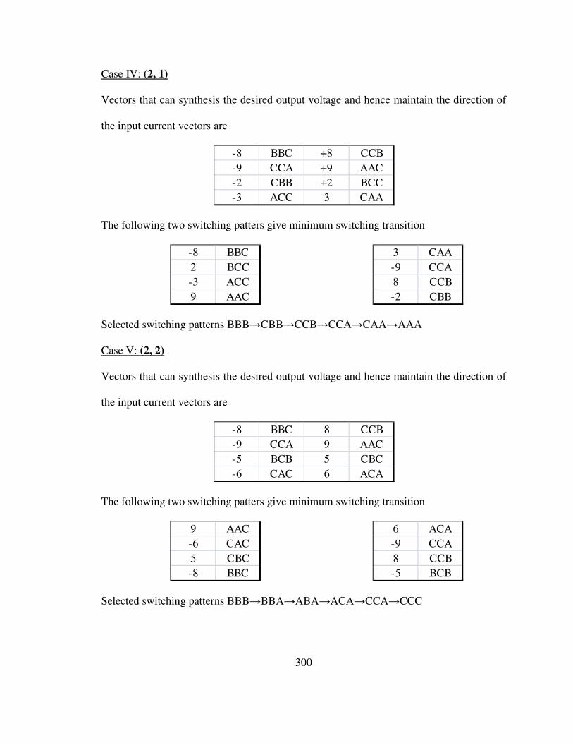
300
Case IV: (2, 1)
Vectors that can synthesis the desired output voltage and hence maintain the direction of
the input current vectors are
The following two switching patters give minimum switching transition
Selected switching patterns BBB→CBB→CCB→CCA→CAA→AAA
Case V: (2, 2)
Vectors that can synthesis the desired output voltage and hence maintain the direction of
the input current vectors are
The following two switching patters give minimum switching transition
Selected switching patterns BBB→BBA→ABA→ACA→CCA→CCC
-8 BBC +8 CCB
-9 CCA +9 AAC
-2 CBB +2 BCC
-3 ACC 3 CAA
-8 BBC
2 BCC
-3 ACC
9 AAC
3 CAA
-9 CCA
8 CCB
-2 CBB
-8 BBC 8 CCB
-9 CCA 9 AAC
-5 BCB 5 CBC
-6 CAC 6 ACA
9 AAC
-6 CAC
5 CBC
-8 BBC
6 ACA
-9 CCA
8 CCB
-5 BCB

301
Case VI: (2, 3)
Vectors that can synthesis the desired output voltage and hence maintain the direction of
the input current vectors are
The following two switching patters give minimum switching transition
Selected switching patterns BBB→BCB→BCC→ACC→ACA→AAA
Case VII: (3, 1)
Vectors that can synthesis the desired output voltage and hence maintain the direction of
the input current vectors are
-8 BBC 8 CCB
-7 AAB 7 BBA
-1 BAA 1 ABB
-2 CBB 2 BCC
The following two switching patters give minimum switching transition
Selected switching patterns: CCC→CCB→CBB→ABB→AAB→AAA
-5 BCB +5 CBC
-6 CAC +6 ACA
-2 CBB +2 BCC
-3 ACC +3 CAA
-2 CBB
+5 CBC
-6 CAC
+3 CAA
-5 BCB
+2 BCC
-3 ACC
6 ACA
2 BCC
-8 BBC
7 BBA
-1 BAA
8 CCB
-2 CBB
1 ABB
-7 AAB

302
Case VIII: (3, 2)
Vectors that can synthesis the desired output voltage and hence maintain the direction of
the input current vectors are:
The following two switching patterns give minimum switching transition
Selected switching patterns: CCC→CCB→BCB→BAB→AAB→AAA
Case IX: (3, 3)
Vectors that can synthesis the desired output voltage and hence maintain the direction of
the input current vectors are:
The following two switching patterns give minimum switching transition
Selected switching patterns: CCC→CBC→CBB→ABB→ABA→AAA
-5 BCB 5 CBC
-4 ABA 4 BAB
-8 BBC 8 CCB
-7 AAB 7 BBA
+5 CBC
-8 BBC
+7 BBA
-4 ABA
+8 CCB
-5 BCB
4 BAB
-7 AAB
-5 BCB +5 CBC
-4 ABA +4 BAB
-1 BAA +1 ABB
-2 CBB +2 BCC
+2 BCC
-5 BCB
+4 BAB
-1 BAA
+5 CBC
-2 CBB
1 ABB
-4 ABA

303
Case X: (1, 4)
Vectors that can synthesis the desired output voltage and hence maintain the direction of
the input current vectors are
The following two switching patterns give minimum switching transition
Case XI: (6, 5)
Vectors that can synthesis the desired output voltage and hence maintain the direction of
the input current vectors are
The following two switching patterns give minimum switching transition
The switching pattern has summarized for an input current lie on sector one and for all
possible output voltage sectors are shown below.
-7 AAB 7 BBA
-9 CCA 9 AAC
-3 ACC 3 CAA
-1 BAA 1 ABB
-9 CCA
3 CAA
-1 BAA
7 BBA
+1 ABB
-7 AAB
+9 AAC
-3 ACC
-5 BCB 5 CBC
-4 ABA 4 BAB
-8 BBC 8 CCB
-7 AAB 7 BBA
5 CBC
-8 BBC
7 BBA
-4 ABA
8 CCB
-5 BCB
4 BAB
-7 AAB

304
The final switching patterns are
(1,1) (1,2) (1,3) (1,4) (1,5) (1,6)
CCA→CAA→ BAB→AAB→ CAC→CAA→ CCA→CAA→ BAB→AAB→ CAC→CAA→
BAA→BBA AAC→CAC BAA→BAB BAA→BBA AAC→CAC BAA→BAB
ABB→AAB→ BBA→AB→ ACC→ACA→ ABB→AAB→ BBA→ABA→ ACC→ACA→
AAC→ACC ACA→CCA ABA→ABB AAC→ACC ACA→CCA ABA→ABB
1 +9 -7 -3 +1 -6 +4 +9 -7 +3 -1 -6 +4 -9 +7 +3 -1 +6 -4 -9 +7 -3 +1 +6 -4
2 -8 +9 +2 -3 +5 -6 -8 +9 -2 +3 +5 -6 +8 -9 -2 +3 -5 +6 +8 -9 +2 -3 -5 +6
3 +7 -8 -1 +2 -4 +5 +7 -8 +1 -2 -4 +5 -7 +8 +1 -2 +4 -5 -7 +8 -1 +2 +4 -5
4 -9 +7 +3 -1 +6 -4 -9 +7 -3 +1 +6 -4 +9 -7 -3 +1 -6 +4 +9 -7 +3 -1 -6 +4
5 +8 -9 -2 +3 -5 +6 +8 -9 +2 -3 -5 +6 -8 +9 +2 -3 +5 -6 -8 +9 -2 +3 +5 -6
6 -7 +8 +1 -2 +4 -5 -7 +8 -1 +2 +4 -5 +7 -8 -1 +2 -4 +5 +7 -8 +1 -2 -4 +5
t1 t2 t3 t4 t1 t2 t3 t4 t1 t2 t3 t4 t1 t2 t3 t4 t1 t2 t3 t4 t1 t2 t3 t4
In p
ut
Cu
rren
t
Vec
tor
Sec
tor
Sector of output voltage vector
1 2 3 4 5 6
Times

305
APPENDIX E
REFERENCE FRAME TRANSFORMATION OF MODULATION
SIGNALS
The objective of this derivation is to obtain an expression of the modulation
signals in qd transformation. Then it possible to write an explicit expression for the
mapping between the input and output currents of a matrix converter in a qd reference
frame. Similarly, the output voltage can also be written in terms of the input capacitor
voltages using the qd reference frame. The relationship between the input and output
currents of a matrix converter in terms of the switching signals are given as
cscCbscBascAcp
csbCbsbBasbAbp
csaCbsaBasaAap
ISISISI
ISISISI
ISISISI
++=
++=
++=
(E.1)
The output voltage can be calculated from the input filter capacitor voltage and the
switching function as:
cpcCbpbCapaCcs
cpcBbpbBapaBbs
cpcAbpbAapaAas
VSVSVSV
VSVSVSV
VSVSVSV
++=
++=
++=
(E.2)
There are two transformations carried out in this analysis: the input side and output side
transformations K(θp) and K(θs) where θop and θos are their corresponding initial angle of
the reference frames respectively.
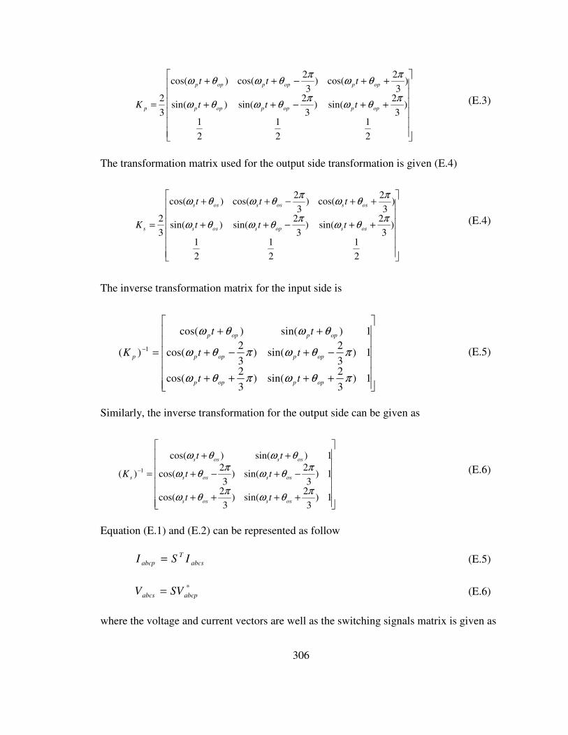
306
++−++
++−++
=
2
1
2
1
2
1
)3
2sin()
3
2sin()sin(
)3
2cos()
3
2cos()cos(
3
2 πθω
πθωθω
πθω
πθωθω
oppoppopp
oppoppopp
p ttt
ttt
K (E.3)
The transformation matrix used for the output side transformation is given (E.4)
++−++
++−++
=
2
1
2
1
2
1
)3
2sin()
3
2sin()sin(
)3
2cos()
3
2cos()cos(
3
2 πθω
πθωθω
πθω
πθωθω
ossopsoss
ossossoss
s ttt
ttt
K (E.4)
The inverse transformation matrix for the input side is
++++
−+−+
++
=−
1)3
2sin()
3
2cos(
1)3
2sin()
3
2cos(
1)sin()cos(
)( 1
πθωπθω
πθωπθω
θωθω
oppopp
oppopp
oppopp
p
tt
tt
tt
K (E.5)
Similarly, the inverse transformation for the output side can be given as
++++
−+−+
++
=−
1)3
2sin()
3
2cos(
1)3
2sin()
3
2cos(
1)sin()cos(
)(1
πθω
πθω
πθω
πθω
θωθω
ossoss
ossoss
ossoss
s
tt
tt
tt
K (E.6)
Equation (E.1) and (E.2) can be represented as follow
abcs
T
abcp ISI = (E.5)
*
abcpabcs SVV = (E.6)
where the voltage and current vectors are well as the switching signals matrix is given as
307
=
=
=
=
cp
bp
ap
abcp
cs
bs
as
abcs
cp
bp
ap
abcp
cs
bs
as
abcs
V
V
V
V
I
I
I
I
I
I
I
I
V
V
V
V
The nine switching functions can be represented in matrix form as
=
cCbCaC
cBbBaB
cAbAaA
SSS
SSS
SSS
S (E.7)
Define the following qd input and output voltage and current vectors as
abcppqdop
abcppqdop
IKI
VKV
=
=
abcssqdos
abcssqdos
IKI
VKV
=
=
The synchronous reference frame equations corresponding to (E.5) through (E.6) is given
below:
qdosqdoIqdoss
T
pqdop IMIKSKI == −1)( (E.8)
**1)( qdopqdoVqdoppsqdos VMVKSKV == − (E.9)
From (E8),
1)( −= s
T
pqdoI KSKM (E.10)
Since the averaged switching signals can be expressed as
p
ip
p
npjs
ijV
V
V
VVS
++=
3
2
3
1 (E.11)
Separating (E.11) into two components as follow
*
p
ip
ipV
VS =
and *
p
npjs
jsV
VVS
+= (E.12)

308
where
[ ]cpbpapip
Cs
Bs
As
js SSSS
S
S
S
S =
=
Using (E.12) the expression for the averaged switching signals can be modified as
ipjsij SSS3
2
3
1+= (E.13)
Using the following switching arrays
[ ]CsBsAsjs
cp
bp
ap
T
ip SSSS
S
S
S
S =
= )()(
The expression given in (E.13) can also be given as
[ ]CsBsAs
cp
bp
ap
SSS
S
S
S
IS
+=3
2
3
1 (E.14)
where I is the identity matrix, substituting (E.13) into (E.10)
11
1
)(3
2)(
3
1
))()(3
2
3
1(
−−
−
+=
+=
s
T
js
T
ippsp
s
T
ipjspqdoI
KSSKKIK
KSSIKM
(E.15)
Using the property of transpose of a matrix (AB)T
= BTA
T
Substituting the transformation matrices given in (E.3) to (E.6)

309
++++
−+−+
++
++−++
++−++
=−
1)3
2sin()
3
2cos(
1)3
2sin()
3
2cos(
1)sin()cos(
111
111
111
2
1
2
1
2
1
)3
2sin()
3
2sin()sin(
)3
2cos()
3
2cos()cos(
3
2
3
1)(
3
1 1
πθωπθω
πθωπθω
θωθω
πθωπθωθω
πθωπθωθω
ossoss
ossoss
ossoss
oppoppopp
oppoppopp
sp
tt
tt
tt
ttt
ttt
xKIK
Simplifying the above expression
1
1
100
000
000
)(3
1kKIK sp =
=− (E.16)
Using the input and output side transformation
( )( )11 )()( −− = s
T
js
T
ipps
T
js
T
ipp KSSKKSSK (E.17)
The transformed array of switching signals corresponding to the input side and output
side respectively are given as
T
ippqdop SKS = (E.18)
issqdos SKS = (E.19)
From (E.8)
qdossjsjssqdos MKSSKM1)( −=⇒= (E.20)
T
s
T
qdos
T
qdoss
T
js KMMKS ))(()())(( 11 −− == (E.21)

310
T
s
T
qdos
T
js KMS ))(()( 1−= (E.22)
Similarly,
111 )())(()()( −−− = s
T
s
T
qdosqdopsjsipp KKMMKSSK (E.23)
Substituting the transformation matrices given in (E.3) to (E.6)
++++
−+−+
++
++++
−+−+
++
=−−
1)3
2sin()
3
2cos(
1)3
2sin()
3
2cos(
1)sin()cos(
1)3
2sin()
3
2cos(
1)3
2sin()
3
2cos(
1)sin()cos(
)())(( 11
πθωπθω
πθωπθω
θωθω
πθωπθω
πθωπθω
θωθω
ossoss
ossoss
ossoss
T
ossoss
ossoss
ossoss
s
T
s
tt
tt
tt
tt
tt
tt
KK
Multiplying the above matrices
2
11
200
010
001
2
3)())(( kKK s
T
s =
=−− (E.24)
Substituting (E.24) to (E.23)
I
T
qdosqdopsjsipp kMMKSSK 2
1 )()( =− (E.25)
Using (E.25) and (E.16)
I
T
qdosqdopIqdoI kMMkM 21 )(3
2+= (E.26)

311
Using similar approach,
1))(3
2
3
1( −+= pipjssqdoV KSSIKM
))()((3
2)(
3
1 11 −− += pipjsspsqdoV KSSKKIKM (E.27)
Substituting the transformation matrices given in (E.3) to (E.6) in the above expression
++++
−+−+
++
++−++
++−++
=−
1)3
2sin()
3
2cos(
1)3
2sin()
3
2cos(
1)sin()cos(
111
111
111
2
1
2
1
2
1
)3
2sin()
3
2sin()sin(
)3
2cos()
3
2cos()cos(
3
2
3
1)(
3
1 1
πθωπθω
πθωπθω
θωθω
πθωπθωθω
πθωπθωθω
osposp
osposp
osposp
opsopsops
opsopsops
ps
tt
tt
tt
ttt
ttt
xKIK
Simplifying the above matrix multiplication,
1
1
100
000
000
)(3
1kKIK sp =
=− (E.28)
Simplifying the second term given in (E.27)
jssqdos SKM = (E.29)

312
qdopp
T
ip
T
ippqdop MKSSKM1)( −=⇒=
T
p
T
qdop
T
qdoppipqdopp
T
ip KMMKSMKS ))(())(()( 111 −−− ==⇒=
Therefore the following equation holds true
))())(()(())()(( 111 −−− = p
T
p
T
qdopqdospipjss KKMMKSSK (E.30)
Substituting the transformation matrices given in (E.3) to (E.6)
++++
−+−+
++
++++
−+−+
++
=−−
1)3
2sin()
3
2cos(
1)3
2sin()
3
2cos(
1)sin()cos(
1)3
2sin()
3
2cos(
1)3
2sin()
3
2cos(
1)sin()cos(
)())(( 11
πθωπθω
πθωπθω
θωθω
πθωπθω
πθωπθω
θωθω
osposp
osposp
osposp
T
osposp
osposp
osposp
p
T
p
tt
tt
tt
tt
tt
tt
KK
The above matrix multiplication gives,
vp
T
p kKK 2
11
200
010
001
2
3)())(( =
=−− (E.31)
Therefore, the q-d-o equations of the modulation signals are:
V
T
qdopqdosVqdoV kMMkM 21 )(γ+= (E.32)
I
T
qdosqdopIqdoI kMMkM 21 )(γ+= (E.33)

313
Calculation of Mqdov is shown below
*
p
npjs
jsV
VVS
+= (E.34)
Let the balanced output voltage is given as follows where Vn is the magnitude of the
output voltage.
)cos( onsnan tVV θω += (E.35)
)3
2cos(
πθω −+= onsnan tVV (E.36)
)3
2cos(
πθω ++= onsnan tVV (E.37)
onθ is the initial angle of the output phase voltage and the three phase balanced input
capacitor voltage are
)cos( omppap tVV θω += (E.38)
)3
2cos(
πθω −+= omppbp tVV (E.39)
)3
2cos(
πθω ++= omppcp tVV (E.40)
omθ is the initial angle of the input capacitor voltage
++−++
++−++
==
Cs
Bs
As
ossopsoss
ossossoss
jssqdos
S
S
S
ttt
ttt
SKM
2
1
2
1
2
1
)3
2sin()
3
2sin()sin(
)3
2cos()
3
2cos()cos(
3
2πθωπθωθω
πθωπθωθω

314
Substituting (E.34) into the expression given above
+
+
+
++−++
++−++
=
*
*
*
2
1
2
1
2
1
)3
2sin()
3
2sin()sin(
)3
2cos()
3
2cos()cos(
3
2
p
npcn
p
npbn
p
npan
ossopsoss
ossossoss
qdos
V
VV
V
VV
V
VV
ttt
ttt
M πθωπθωθω
πθωπθωθω
Multiplying the two terms
+++
+++−+++
+++−+++
=
npcnbnan
osscnossbnossan
osscnossbnossan
p
qdos
VVVV
tVtVtV
tVtVtV
VM
2
3)(
2
1
)3
2sin()
3
2sin()sin(
)3
2cos()
3
2cos()cos(
3
2
0
*
4434421
πθωπθωθω
πθωπθωθω
(E.41)
Simplifying the first and the second elements of the array
)sin(2
3
)3
2sin()
3
2cos(
)3
2sin()
3
2cos()sin()cos(
)3
2sin()
3
2sin()sin(
oson
n
onsonscn
ossonsnossonsn
osscnossbnossan
V
ttV
ttVttV
tVtVtV
θθ
πθω
πθω
πθω
πθωθωθω
πθω
πθωθω
−−=
++++
+−+−++++=
+++−+++
Therefore
−−
−
=
−−
−
=
=
np
oson
p
n
oson
p
n
np
oson
n
oson
n
p
os
ds
qs
qdos
V
V
V
V
V
V
V
V
VM
M
M
M )sin(
))cos(
2
3
)sin(2
3
))cos(2
3
3
2*
*
*θθ
θθ
θθ
θθ
(E.42)
315
Therefore the qdo axis component of the modulation signal corresponding with the output
side can be given as
*
*
*
)sin(
)cos(
p
np
os
oson
p
nds
oson
p
nqs
V
VM
V
VM
V
VM
=
−−=
−=
θθ
θθ
(E.43)
The expression for Mqdop can be analyzed as follows
++−++
++−++
==
Cs
Bs
As
oppoppopp
oppoppopp
ippqdop
S
S
S
ttt
ttt
SKM
2
1
2
1
2
1
)3
2sin()
3
2sin()sin(
)3
2cos()
3
2cos()cos(
3
2πθωπθωθω
πθωπθωθω
Simplifying the above analysis
++
+++−+++
+++−+++
=
44 344 210
***
*
)(2
1
)3
2sin()
3
2sin()sin(
)3
2cos()
3
2cos()cos(
3
2
cpbpap
oppcpoppbpoppap
oppcpoppbpoppap
p
qdop
VVV
tVtVtV
tVtVtV
VM πθωπθωθω
πθωπθωθω
Using similar simplification used for (E.42),
−−
−
=
=
0
)sin(
))cos(
opom
opom
op
dp
qp
qdop
M
M
M
M θθ
θθ
(E.44)

316
Therefore qdo components of the modulation signals related to the input side are given as
0
)sin(
)cos(
=
−−=
−=
op
osondp
osonqp
M
M
M
θθ
θθ
(E.45)
And
−−
−
=
0
)sin(
))cos(
opom
opom
op
dp
qp
M
M
M
θθ
θθ
(E.46)
The expression for MqdoV becomes
V
T
qdopqdosVqdoV kMMkM 21 )(3
2+=
Substituting (E.42) and (E.44) into (E.47)
−−
−
−−
−
+
=
200
010
001
2
3
0
)sin(
)cos(
)sin(
))cos(
3
2
100
000
000
*
*T
opom
opom
np
oson
p
n
oson
p
n
qdoV
V
V
V
V
V
M θθ
θθ
θθ
θθ
The synchronous reference frame modulation signals which map the input and output
three phase voltages are
−−−
−−−−−
−−−−−
=
1)sin()cos(
0)sin()sin()cos()sin(
0)sin()cos()cos()cos(
opomnpopomnp
opomoson
p
n
opomoson
p
n
opomoson
p
n
opomoson
p
n
qdoV
VV
V
V
V
V
V
V
V
V
M
θθθθ
θθθθθθθθ
θθθθθθθθ
(E.47)

317
The expression for MqdoI
I
T
qdosqdopIqdoI kMMkM 21 )(γ+= (E.47)
Substituting (E.42) and (E.44) into (E.47)
−−
−
−−
−
+
=
200
010
001
2
3)sin(
)cos(
0
)sin(
)cos(
3
2
100
000
000
*
*
T
np
oson
p
n
oson
p
n
opom
opom
qdoI
V
V
V
V
V
M θθ
θθ
θθ
θθ
Similarly the synchronous reference frame modulation signals which maps the input and
output three phase currents are
−−−−−
−−−−−
=
100
2)sin()sin()sin()cos(
2)cos()sin()cos()cos(
npopomoson
p
nopomoson
p
n
npopomoson
p
nopomoson
p
n
qdoI VV
V
V
V
VV
V
V
V
M θθθθθθθθ
θθθθθθθθ
(E.48)
omθ is initial angle of input capacitor voltage
opθ is initial angle of input side transformations
onθ is initial angle of output voltage
osθ is initial angle of output side transformations
Define
p
n
V
VM =

318
The four components of the modulation signals which are used extensively in this work are
given as follow.
)cos()cos( opomosonqq MM θθθθ −−= (E.38)
)cos()sin( opomosonqd MM θθθθ −−= (E.38)
)sin()cos( opomosondq MM θθθθ −−= (E.38)
)sin()sin( opomosondd MM θθθθ −−= (E.38)

319
APPENDIX F
FOURIER SERIES REPREESNTATION OF A PWM WAVEFORM
FOR A NON-INTEGER MULTIPLE FREQUENCY WITH A NON-
ZERO PHASE ANGLE
A theoretical analysis of the harmonic content of a PWM waveform when the
modulation signal consists of 5th
and 7th
harmonics is presented in [56]. Moreover, a
general solution for harmonic coefficients of a PWM output for a single-phase converter
leg is also given in [58, 81]. In [57], a non-zero phase angle of harmonic content in the
modulation signal is considered the Fourier series analysis; however, it did not show the
effect of phase angle clearly. The objective of this work is to determine the harmonic
coefficients of a PWM output when the modulation signals consist of two harmonics
which are not necessarily to be integer with a non-zero phase angles. The work is applied
to analyze the Fourier series of switching signals for a matrix converter. The modulation
signals consisting of a fundamental and two harmonics which both are non-integer
multiple of the fundamental is given as:
)cos()cos()cos()( boobaooaoo tbMtaMtMtM θωθωθω +++++= (F.1)
where
M is the modulation index for the fundamental component
Ma is the modulation index for the ath
harmonics
Mb is the modulation index for the bth
harmonics

320
oω is the angular frequency of the fundamental component of modulation signal
oθ is the initial angle of the fundamental component of modulation signal
Define ty oω= (F.1) can be written as
)cos()cos()cos()( bobaoao byMayMyMyM θθθ +++++= (F.2)
The coefficient of the furrier series is given by:
( )
( )dxdyeVjBAC
nymxjyM
yMdcmnmnmn
)()(1
2
)(12
22
1 +
−
+
+−∫ ∫=+=π
π
π
ππ
(F.3)
Substituting (F.2) into (F.3),
( )
( )∫ ∫
∫ ∫
−
++++++ −++
− ++++++−
+++
+=
π
π
θθθπ π
ω
ω
π
π θθθπ
π
ω
ω
π
)cos()cos()cos(12
0
')))
2(((
0
)cos()cos()cos(12
')))
2(((
2
''' '
'''
'
2
bofbaofaofc
of
borbaoraor
c
or
byMayMyM
f
xynmxj
byMayMyMr
xynmxjdc
mn
dxdye
dxdyeV
C
(F.4)
Rearranging the expression given in (F.4)
( )
( )∫ ∫
∫ ∫
−
++++++ −
− ++++++−
+
+=
π
π
θθθπ
ω
ωπ
ω
ω
π
π θθθπ
ω
ωπ
ω
ω
π
)cos()cos()cos(12
0
')(
2
0
)cos()cos()cos(12
')(
2
2
''''
'''
'
2
bofbaofaoffc
o
c
o
borbaoraor
rc
o
c
o
byMayMyM
f
jnyxnmjjn
byMayMyMr
jnyxnmjjn
dcmn
dxdyeee
dxdyeeeV
C
(F.5)
Define the following terms,
nmqc
o
ω
ω+= (F.6)
Substituting (F.6) into (F.5)
( )
( )∫ ∫
∫ ∫
−
++++++−
− ++++++−+=
π
π
θθθππ
ω
ω
π
π θθθπ
π
ω
ω
π
)cos()cos()cos(12
0
'2
0
)cos()cos()cos(12
'2
2
''''
'''
'
2
bofbaofaoffc
o
borbaoraor
rc
o
byMayMyM
f
jqxjnyjn
byMayMyMr
jqxjnyjn
dcmn
dxdyeee
dxdyeeeV
C
(F.7)

321
Evaluating the inner integral,
( )
( )
+
=
∫
∫
−
++++++−
− ++++++−
π
π
θθθππ
ω
ω
π
π θθθπ
π
ω
ω
π '''''
'''
'
)cos()cos()cos(12
0
2
'0
)cos()cos()cos(12
2
22fbofbaofaof
fc
o
borbaoraor
rc
o
dybyMayMyMjqxjny
jn
rbyMayMyM
jqxjnyjn
dcmn
eee
dyeee
jq
VC
Solving the inner integral,
( )
( )
+−
+
−
=
∫
∫
−
+++++−
−
++++++−
π
π
θθθππ
ω
ω
π
π
θθθππ
ω
ω
π'
)cos()cos()cos(22
')cos()cos()cos(1
22
2'''
'
''''
1
1
2
f
byMayMyMqjjnyjn
r
byMayMyMqjjny
jn
dcmn
dyeee
dyeee
jq
VC
bofbaofaoffc
o
borbaoraorrc
o
Simplifying the above expression result in
( ) ( ) ( )
( ) ( ) ( )
−
=
∫
∫
−
+++−
−
+−+−+−−
π
π
θπ
θπ
θπππ
ω
ω
π
π
θπ
θπ
θπππ
ω
ω
π'
cos2
cos2
cos222
'cos
2cos
2cos
222
2'''
'
''''
2
f
byqMjayqMjyqMjqjjny
jn
r
byqMjayqMjyqMjqjjny
jn
dc
mn
dyeeeeee
dyeeeeee
jq
VC
bofbaofaofrc
o
borbaoraorrc
o
Using Jacobi-Anger expansion )cos(θξj
e±
can be given in Bessel series expressions as:
)cos()(2)(1
)cos( θξξθξ kJjJek
k
k
o
j ∑∞
=
±± += (F.8)
Using the following properties of Bessel function,
)()1()(
)()(
ξξ
ξξ
n
n
n
nn
JJ
JJ
−=
−=
−
−
(F.9)
)()( ξξ −= oo JJ (F.10)

322
Substituting (F.9) and (F.10) into (F.8)
++
+
+++
−
++
+
+++
=
∫
∑
∑
∑
∫
∑
∑
∑
−
∞
=
−
∞
=
−
∞
=
−
−
−
∞
=
∞
=
∞
=
π
π
π
π
π
π
θππ
θπ
πθ
ππ
θππ
θπ
πθ
ππ
π
''
1
'
1
'
1
2
''
1
'
1
'
1
2
2
)(cos)2
(2)2
((
)cosh()2
(2
)2
()((cos)2
(2)2
((
)(cos)2
(2)2
((
)cosh()2
(2
)2
()((cos)2
(2)2
((
2
'
'
rbor
z
bz
z
bo
aor
h
ah
h
aoor
k
k
k
o
jnyjm
fbof
z
bz
z
bo
aof
h
ah
h
aoof
k
k
k
o
jnyjm
dc
mn
dybyzMqJjMqJ
ayMqJj
MqJykMqJjMqJ
ee
dybyzMqJjMqJ
ayMqJj
MqJykMqJjMqJ
ee
jq
VC
r
f
(F.11)
The expression in (F.11) can be simplified
∫−=π
π
ππππ
π'2
21
'
)2
()2
()2
(2
f
jny
boaoo
jmdc
a dyeMqJMqJMqJejq
VC f (F.12)
)2
sin()2
()2
()2
(2
41
'
11
ππππ
πmRMqJMqJMqJ
q
VCC aboaoo
dcaa =− (F.13)
where the constant is given below
π
π
n
nR a
)sin(1 = (F.14)
∫ ∑−
∞
=
+=π
π
π
θπππ
π''
1
221 )cos()
2()
2()
2(2
2
'
fbof
jny
z
bz
z
aoo
jmdc
b dyzzbyeMqJjMqJMqJejq
VC f (F.15)
Since the following holds true
)(2
1)cos(
''' bofbof jzjzbyjzjzby
f eezbyθθ −−+
+= (F.16)

323
Evaluating the following integral over a period gives
∫−−−+
+π
π
θθ ')(2
1 '''
f
jzjzbyjzjzbyjnydyeee bofboff
( ) ( )∫∫ −
−−
−
++=
π
π
θπ
π
θ ''''
2
1
2
1f
yzbnjjz
f
yznjjzdyeedyee fbofbo
Evaluating the integrals result
π
ππ
π
ππ θθ
)(
))sin((
)(
))sin((
zbn
zbne
zbn
zbne bobo jzjz
−
−+
+
+ − (F.17)
Substituting (F.17) into (F.15)
))(2
sin()2
()2
()2
(2
41
1
'
11 zmRMqJMqJMqJq
VCC b
z
bzaoodc
bb +=− ∑∞
=
ππππ
π (F.18)
where
π
π
π
π θθ
)(
))sin((
)(
))sin((1
zbn
zbne
zbn
zbneR bobo jzjz
b−
−+
+
+= −
(F.19)
Evaluating the second of the two integrals given in (F.11)
))(2
sin()2
()2
()2
(2
42
1
'
22 hmRMqJMqJMqJq
VCC a
h
ahboodc
aa +=− ∑∞
=
ππππ
π (F.20)
where
π
π
π
π θθ
)(
))sin((
)(
))sin((2
han
hane
han
haneR baao jhjh
a−
−+
+
+= −
(F.21)
With the same approaches,
∫∑
∑− ∞
=
∞
=
+
+
=π
π
π
θπ
θππ
π ''
1
'
1222
)cos()2
(
)cos()2
()2
(4
2
'
fbof
z
bz
z
aof
h
ah
h
o
jny
jmdc
b
dyzzbyMqJj
hhayMqJjMqJe
ejq
VC
f
(F.22)

324
Using (F.17) it is possible to evaluate (F.12)
))(2
sin()2
()2
()2
(2
42
1 1
'
22 zhmRMqJMqJMqJq
VCC b
h
ah
z
bzodc
bb ++=− ∑∑∞
=
∞
=
ππππ
π (F.23)
where the constant is given by (F.24)
( ) ( )
( ) ( )
π
π
π
π
π
π
π
π
θθθθ
θθθθ
)(
))sin((
)(
))sin((
)(
))sin((
)(
))sin((2
hazbn
hazbne
hazbn
hazbne
hazbn
hazbne
hazbn
hazbneR
aoboaobo
aoboaobo
hzjhzj
hzjhzj
b
−−
−−+
+−
+−
+−+
−++
++
++=
+−−−
−+
(F.24)
The third terms can be evaluated as follows
))(2
sin()2
()2
()2
(2
43
1
'
33 kmRMqJMqJMqJq
VCC a
k
kaoodc
aa +=− ∑∞
=
ππππ
π
(F.25)
where
π
π
π
π θθ
)(
))sin((
)(
))sin((3
kn
kne
kn
kneR oo jkjk
a−
−+
+
+= −
(F.26)
With a similar approach,
))(2
sin()2
()2
()2
(2
23
1
'
33 kmRMqJMqJMqJjq
VCC a
k
kaoodc
aa +=− ∑∞
=
ππππ
π (F.27
where
( ) ( )
( ) ( )
π
π
π
π
π
π
π
π
θθθθ
θθθθ
)(
))sin((
)(
))sin((
)(
))sin((
)(
))sin((3
kzbn
kzbne
kzbn
kzbne
kzbn
kzbne
kzbn
kzbneR
oboobo
oboobo
kzjkzj
kzjkzj
b
−−
−−+
+−
+−
+−+
−++
++
++=
+−−−
−+
(F.28)
And the rest two terms in (F.11) can be evaluated as follows
))(2
sin()2
()2
()2
(2
44
1 1
'
44 hkmRMqJMqJMqJq
VCC a
h k
ahkbodc
aa ++=− ∑∑∞
=
∞
=
ππππ
π (F.27)

325
where
( ) ( )
( ) ( )
π
π
π
π
π
π
π
π
θθθθ
θθθθ
)(
))sin((
)(
))sin((
)(
))sin((
)(
))sin((4
khan
khane
khan
khane
khan
khane
khan
khaneR
oaooao
oaooao
khjkhj
khjkhj
a
−−
−−+
+−
+−
+−+
−++
++
++=
+−−−
−+
(F.28)
The last expression in (F.11) can be simplified following the same analogy.
∑∑∑∞
=
∞
=
∞
=
+++=−1
4
1 1
'
44 )(2
sin()2
()2
()2
(2
4
k
bk
h
ah
z
bzdc
bb zhkmRMqJMqJMqJq
VCC
ππππ
π (F.29)
where
( ) ( )
( ) ( )
( ) ( )
( ) ( )
π
π
π
π
π
π
π
π
π
π
π
π
π
π
π
π
θθθθθθ
θθθθθθ
θθθθθθ
θθθθθθ
)(
))sin((
)(
))sin((
)(
))sin((
)(
))sin((
)(
))sin((
)(
))sin((
)(
))sin((
)(
))sin((4
khabzn
khabzne
khabzn
khabzne
khabzn
khabzne
khabzn
khabzne
khabzn
khabzne
khabzn
khabzne
khabzn
khabzne
khabzn
khabzneR
oaobooaobo
oaobooaobo
oaobooaobo
oaobooaobo
khzjkhzj
khzjkhzj
khzjkhzj
khzjkhzj
b
−−−
−−−+
+−−
+−−
+−+−
−+−+
++−
++−
+−−+
−−++
+−+
+−+
+−++
−+++
+++
+++=
++−−+−
+−−−−−
−−+−
−+++
(F.30)
Therefore the generalized Fourier coefficient of a single phase leg with a modulation
signals consisting of two non-integer harmonics having a non-zero phase angles are
expressed in (F.31)
The typical single phase inverter leg is shown in Figure F.1 which is used to the
analysis throughout the section. Simulation has been done to verify the analytical result.
The voltage across the load can be given as:
)12()( −=−= pdcnpdcao SVSSVV (F.32)

326
++++
+++
+++
+++
++
++
++
+
=
∑∑∑
∑∑
∑∑
∑∑
∑
∑
∑
∑∑
∞
=
∞
=
∞
=
∞
=
∞
=
∞
=
∞
=
∞
=
∞
=
∞
=
∞
=
∞
=
∞
==
∞
=−∞=
1
4
1 1
4
1 1
3
1 1
2
1 1
3
1
2
1
1
1
1
01
1
),(
)(2
sin()2
()2
()2
(
))(2
sin()2
()2
()2
(
))(2
sin()2
()2
()2
(
))(2
sin()2
()2
()2
(
))(2
sin()2
()2
()2
(
))(2
sin()2
()2
()2
(
))(2
sin()2
()2
()2
(
)2
sin()2
()2
()2
(
1
2
4
k
bk
h
ah
z
bz
a
k h
ahkbo
b
k
ah
z
bzo
b
h
ah
z
bzo
a
k
kaoo
a
h
ahboo
b
z
bzaoo
aboaoo
mm
nn
dc
bamn
zhkmRMqJMqJMqJ
hkmRMqJMqJMqJ
zkmRMqJMqJMqJ
zhmRMqJMqJMqJ
kmRMqJMqJMqJ
hmRMqJMqJMqJ
zmRMqJMqJMqJ
mRMqJMqJMqJ
q
VC thth
ππππ
ππππ
ππππ
ππππ
ππππ
ππππ
ππππ
ππππ
π
(F.31)
Normalizing (F.32) with respect to Vdc
12)( −= pao SpuV (F.33)
First a computer simulation has done to verify the analytical expressions considering
)cos(9.0 tM oω= , 21=o
c
f
f (F.34)
Figure F.2 presents the voltage spectrum for saw tooth naturally sampled PWM for the
condition of a carrier ration of 21 and a modulation index of 0.9. The plots shows the
single fundamental and low frequency component produced by the modulation process,
and the group of sideband harmonics around the first carrier group (around 21) and
second carrier group (around 42) carrier group and one sideband harmonics of the triple
carrier (around 63).

327
(a) (b)
Figure F.1 (a) Single phase inverter leg, (b) carrier signal
Figure F.2 Theoretical results based on derived expressions
0 10 20 30 40 50 6010
-4
10-3
10-2
10-1
100
Harmonic Number

328
Figure F.3 FFT results-a simulation time of 1/400 times the switching frequency.
Figure F.4 Symmetrical regular sampling.
0 10 20 30 40 50 6010
-4
10-3
10-2
10-1
100
Harmonic Number
0 0.5 1 1.5 2 2.5 3 3.5 4 4.5 5
x 10-3
-1
-0.8
-0.6
-0.4
-0.2
0
0.2
0.4
0.6
0.8
1
Time
329
Figure F.5 Asymmetrical regular sampling.
Effect of Sampling on the output voltage spectrum
The modulation signals consist of fundamental, 5th
and 7th
harmonics with their
magnitude of M = 0.3, M5 = 0.24 and, M7 = 0.4; and the phase angles of each signals are
assumed to be zero. 50=o
c
f
f. There are basically three types of sampling techniques, the
natural sampling (without sampling the modulation signals), the symmetrically regular
sampling and asymmetrically regular sampling. Figure F.6 shows the output voltage
spectrum under natural sampling. The voltage spectrum based on the regular sampling is
shown in Figure F.6 and F.7. As shown in Figure F.7, symmetrical regular sampling
creates additional side band harmonics around the carrier.
0 0.5 1 1.5 2 2.5 3 3.5 4 4.5 5
x 10-3
-1
-0.8
-0.6
-0.4
-0.2
0
0.2
0.4
0.6
0.8
1
Time

330
Figure F.6 FFT results for natural sampling
Figure F.7 FFT results for symmetrical regular sampling
0 10 20 30 40 50 60 70 80 90 10010
-4
10-3
10-2
10-1
100
Harmonic Number
0 10 20 30 40 50 60 70 80 90 10010
-4
10-3
10-2
10-1
100
Harmonic Number

331
Figure F.8 FFT results for asymmetrical regular sampling
The voltage spectrum based on the asymmetrically sampled PWM is also given in
Figure F.8 which is more or less similar to the naturally sampled PMW with attenuated
low order harmonics.
Observation:
• Regular sampling creates low-order baseband harmonics just above the
fundamental component.
• Comparing the natural and regular sampled PWM, it is seen that regular sampled
modulation process attenuates the lower sideband harmonics and increases the
high-side sideband harmonics around the carrier frequency.
0 10 20 30 40 50 60 70 80 90 10010
-4
10-3
10-2
10-1
100
Harmonic Number

332
• Comparing symmetrically and asymmetrically regular sampling, symmetrical
regular sampled PWM causes additional sideband harmonic components to be
present in the output voltage spectra while asymmetrical sampled PWM and
naturally sampled PWM do not create these components.
Figure 9 shows the output voltage spectrum for a modulation signal containing two non-
integer harmonics, 4.5 and 7.5. The ratio of the fundamental and carrier frequencies are
considered to be non-integer, 62.5. The phase angle of the fundamental as well as the
harmonics considered zero. The dominant frequency components around the first carrier
group for the FFT result shown in Figure F.9 are
)2when (;5.60 oc fffn ±==
))7.7(when (;8.53 ooc ffffn +±==
))5.47.7(when (;3.59 ooc ffffn −±==
)5.4(2when (;5.53 oc fffn ±==
))5.4(when (;59 ooc ffffn −±==
))7.75.4(when (;3.50 ooc ffffn +±==
))5.4(when (;57 ooc ffffn +±==
))7.7(2when (;1.47 oc fffn ±==
)7.7(when (;8.55 ooc ffffn −±==
The effect of non-zero phase angle of the modulation signals are demonstrated
considering three cases. Figure F.10 shows when the phase angles of the modulation
signals are zeros. If the addition of the phase angles shifts the operation region into over

333
modulation, the resulting output voltage spectrum will introduce an odd harmonics in the
baseband frequency and even harmonics around the first carrier group. When these phase
angles are different from zero and they do not affect the linear operation region, the
output voltage spectrum is generally affected by the phase angle. However, this voltage
contains low magnitude sideband and baseband harmonics as shown in Figure F.12. IT is
necessary to note that the above figurers are obtained using a non-integer carrier-to-
fundamental frequency ratio. The effect of these phase angles are more exemplified
considering a integer carrier-to-fundamental frequency ratio.

323
Figure F.9 Output voltage spectrum with modulation signal containing two non-integer harmonics a and b with 50=of ,
5.62=o
c
f
f, 5.4=a and 7.7=b
0 10 20 30 40 50 60 70 8010
-4
10-3
10-2
10-1
100
Ha
rmo
nic
Ma
gn
itu
de
Harmonic Number
50 52 54 56 58 60 6210
-4
10-3
10-2
10-1
100
Ha
rmo
nic
Ma
gn
itu
de
Harmonic Number

324
Figure F.10 FFT of output voltage for the phase angles of the harmonic in the modulation are zero
)7sin(3.0)5sin(4.0)sin(6.0 tttM ooo ωωω ++=
50=of , 5.62=o
c
f
f
1 1.005 1.01 1.015 1.02 1.025 1.03 1.035 1.04-1
-0.5
0
0.5
1
Time
M
0 10 20 30 40 50 60 70 8010
-4
10-3
10-2
10-1
100
Ha
rmo
nic
Ma
gn
itu
de
Harmonic Number
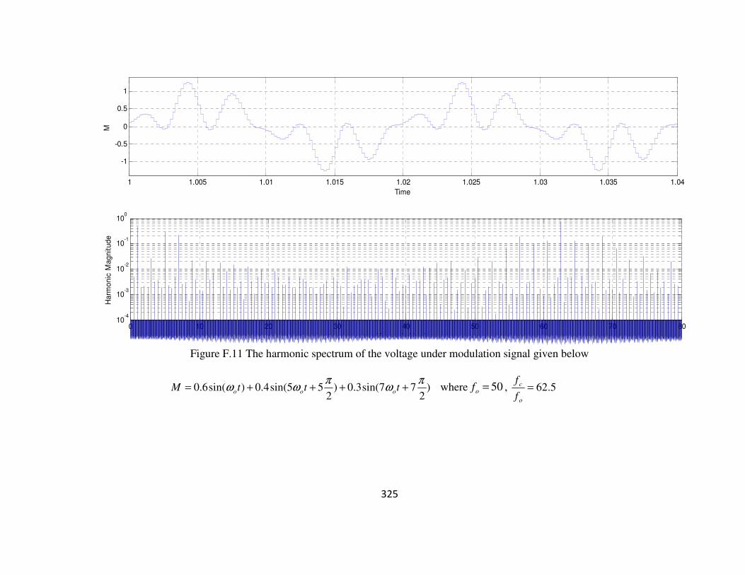
325
Figure F.11 The harmonic spectrum of the voltage under modulation signal given below
)2
77sin(3.0)2
55sin(4.0)sin(6.0π
ωπ
ωω ++++= tttM ooo where 50=of , 5.62=
o
c
f
f
1 1.005 1.01 1.015 1.02 1.025 1.03 1.035 1.04
-1
-0.5
0
0.5
1
Time
M
0 10 20 30 40 50 60 70 8010
-4
10-3
10-2
10-1
100
Ha
rmo
nic
Ma
gn
itu
de
Harmonic Number

326
Figure F.12 Effect of the phase angle of the harmonics on the modulation signals in the linear modulation region.
)2
7sin(3.0)2
5sin(4.0)sin(6.0π
ωπ
ωω ++++= tttM ooo where 50=of , 5.62=
o
c
f
f
1 1.005 1.01 1.015 1.02 1.025 1.03 1.035 1.04-1
-0.5
0
0.5
1
Time
M
0 10 20 30 40 50 60 70 8010
-4
10-3
10-2
10-1
100
Ha
rmo
nic
Ma
gn
itu
de
Harmonic Number

327
(a)
(b)
0 10 20 30 40 50 6010
-4
10-3
10-2
10-1
100
Ha
rmo
nic
Ma
gn
itu
de
0 10 20 30 40 50 6010
-4
10-3
10-2
10-1
100
Ha
rmo
nic
Ma
gn
itu
de
Harmonic Number

328
(c)
Figure F.13 Effect of phase angle of harmonics in the modulation signal when the carrier frequency ratio is Integer
(a) The modulation signal: )7sin(3.0)5sin(4.0)sin(6.0 tttM ooo ωωω ++= (b) The modulation signal:
)2
77sin(3.0)2
55sin(4.0)sin(6.0π
ωπ
ωω ++++= tttM ooo (c) )
27sin(3.0)
25sin(4.0)sin(6.0
πω
πωω ++++= tttM ooo
where 50=of , 50=o
c
f
f
0 10 20 30 40 50 6010
-4
10-3
10-2
10-1
100
Ha
rmo
nic
Ma
gn
itu
de
Harmonic Number

329
Observation:
• The effect of phase angle on the voltage spectrum was seen from two perspectives; the first case is when the addition of
these phase angle will not affect the linear operation region: and the second case is when these phase angle shift the
modulation region from linear to over modulation.
• When the phase angles do not affect the linear operation region, their effect on the output voltage spectrum is not
significant, it only add low order inter-harmonics both in sideband as well as the low frequency baseband.
• If the addition of these phase lead to over modulation region, the harmonics in the modulation signals has two major
effects on the output voltage spectrum:
o Introduce odd frequency around the base band region, such as: 3rd
, 9th
, 11th
……
o Add the even harmonics around the first carrier group.

330
VITA
Melaku Mihret received his Bachelor of Science degree in Electrical and
Computer Engineering from Addis Ababa University, Ethiopia in August 2007. From
November 2007 to August 2009, he worked as an Assistant Lecturer in the Department of
Electrical and Computer Engineering, Hawassa University, Ethiopia. In September 2009,
he joined the Masters program at Tennessee Technological University and he is now
towards completing his Masters Degree in December 2011. His research interests include
Power Electronics Converters, Renewable Energy Systems and Adjustable Speed Drives.