models and simulation of emc problems
TRANSCRIPT

Dipl.-Ing. Susanne Maria Bauer, BSc
Models and simulation of EMC problems
DOCTORAL DISSERTATION
for obtaining the academic degree of doctor of technical sciences
submitted to the
Graz University of Technology
Supervisor/First reviewer
Univ.-Prof. Dipl.Ing Dr.techn. Oszkár Bíró
Institute of Fundamentals and Theory in Electrical Engineering
Second reviewer
Univ.-Prof. Dipl.-Ing. Dr.-techn. József Pávó
Budapest University of Technology and Economics
Graz, January 2021


- 1 -
EIDESSTATTLICHE ERKLÄRUNG
Ich erkläre an Eides statt, dass ich die vorliegende Arbeit selbstständig verfasst, andere
als die angegebenen Quellen/Hilfsmittel nicht benutzt und die den benutzten Quellen
wörtlich und inhaltlich entnommene Stellen als solche kenntlich gemacht habe.
Graz, am …………………………… ………………………………………………..
(Unterschrift)
STATUTORY DECLARATION
I declare that I have authored this thesis independently, that I have not used other than
the declared sources / resources, and that I have explicitly marked all material which has
been quoted either literally or by content from the used sources.
…………………………… ………………………………………………..
date (signature)

- 2 -
Abstract
This work deals with different model development approaches in the topic of electro-
magnetic compatibility (EMC) and the simulation therein, using numerical techniques
like the Finite Element Method (FEM) and the transmission-line modelling for multi-
conductor transmission-lines that can be applied in circuit simulators.
One major focus of this work is the transfer impedance of shielded cables with braided
shields. With the aid of the FEM, the geometry- and material parameters can be mod-
elled very precisely and also the influence of parameter variations on the transfer im-
pedance can be analysed with this simulation approach. Based on the numerical solu-
tion, a simple circuit-simulator model and a new measurement technique are developed.
Also existing analytical approaches for the transfer impedance have been studied in
more detail with the aid of the numerical results. Usually, the analytical models are
compared to measured results but this limits the possible range of geometry- and mate-
rial parameter variations that are of interest for example in case of stretched or pinched
cables. It is shown that, using numerical simulations, these restrictions can be eliminat-
ed.
Another very important topic in the field of EMC are fast transients and conducted
emission and, therefore, the standardized measurement setup for conducted emission for
cable harnesses called the Capacitive Coupling Clamp has been modelled with FEM.
The multi-transmission-line parameters for the circuit-simulator model are extracted
with the usage of this framework as well and the results are compared to measured data
of the same setup. The simulated and measured results stand in excellent agreement.
Also relevant in the context of electrical fast transient disturbances, overvoltage protec-
tion devices such as transient voltage suppressor diodes and especially their modelled
behaviour in spice-like simulators are investigated as well. This investigation of existing
models shows that knowledge of the implemented models is crucial for correct usage
and, as a consequence, for reliable simulation results.

- 3 -
Kurzfassung
Diese Arbeit befasst sich mit diversen Anwendungen im Bereich der elektromagneti-
schen Verträglichkeit (EMV) und deren Simulation mit Hilfe numerischer Methoden
wie der Finite-Elemente-Methode (FEM) und mit Simulationsansätzen wie der Lei-
tungstheorie-Modellierung für Mehrleitersysteme, welche in Netzwerksimulatoren an-
gewendet werden können.
Ein wichtiger Punkt ist die Untersuchung der Transferimpedanz von Geflechtschirmen
von geschirmten Kabeln. Die notwendigen Geometrie- und Materialparameter können
mit Einsatz der FEM sehr präzise modelliert und simuliert werden. Basierend auf den
numerischen Simulationen wurde ein Netzwerkmodell für Netzwerksimulatoren und
eine neue Messmethode der Transferimpedanz entwickelt. Die existierenden analyti-
schen Modelle konnten mit den Ergebnissen der numerischen Simulation ebenfalls für
Parametervariationen untersucht werden. Üblicherweise werden die Modelle mit Mes-
sungen von Standard-Koaxialkabeln verifiziert, was in diesem Fall aber die Parameter-
variationen wie Geometrieabweichungen für z.B. den Fall von gestreckten oder ge-
quetschten Kabeln und auch Materialänderungen nicht so einfach darstellen kann.
Ein weiteres wichtiges Thema in der EMV sind leitungsgebundene Störungen und
schnelle transiente Störsignale. In diesem Kontext wird der standardisierte Messaufbau
der sogenannten Kapazitiven Koppelzange implementiert, welche zur Untersuchung
von leitungsgebundenen Störungen verwendet wird. Für dieses Mehrleitersystem wur-
den die Leitungsparameter mit Hilfe der FEM für ein Netzwerksimulator-Modell extra-
hiert und die simulierten Ergebnisse mit Messungen verifiziert und die Ergebnisse
stimmen ausgezeichnet überein.
Zusätzlich werden Überspannungsschutzelemente gegen diese schnellen transienten
Störungen, wie die Transient-Voltage-Suppressor-Diode und im speziellen deren Mo-
dellierung in LTspice, untersucht. Hier werden die Unterschiede der verschiedenen Mo-
delle in Bezug auf deren Anwendungsbereiche für korrekte Simulationsergebnisse dis-
kutiert.

- 4 -
Acknowledgments
First of all, I would like to thank my former head of the institute and PhD supervisor
Univ.-Prof. Dipl.-Ing. Dr.techn. Oszkár Bíró for his cooperation and support.
It is an honour for me to be allowed to dissertate at this institute where, among others,
renowned scientific paragons such as Oszkár Bíró, Kurt Preis and Werner Renhart are
active, all of whom I was also allowed to count among my colleagues.
I also want thank my colleagues, DI. Dr.techn. Christian Türk, ObstltdhmtD and Ass.
Prof. Dipl.-Ing. Dr.techn. Gunter Winkler (Institute of Electronics), for the excellent and
pleasant collaboration.
I would also like to thank all my colleagues and especially Univ.-Prof. Dipl.-Ing.
Dr.techn. Manfred Kaltenbacher.
A big thank you goes of course to my parents, who have always supported me with infi-
nite patience.
And last but not least, I want to say thank you:
to my neighbours Kathi and Tom. Without them I probably would have had almost only
conversations with my cats during the COVID lockdown,
to Peter Miesbauer, for years of friendship that has withstood all stressful moments,
to Klaus Roppert, for stimulating discussions of technical and general nature
to Astrid, Manuela, Alexandra, Edith and Robert, for uplifting coffee breaks
and to all those who have accompanied me in one way or another over the past years.
“yesterday's weirdness is tomorrow's reason why”
Hunter S. Thompson

- 5 -
Danksagung
Ich möchte mich zuerst bei meinem ehemaligen Institutsleiter und PhD Betreuer Univ.-
Prof. Dipl.-Ing. Dr.techn. Oszkár Bíró für seine Zusammenarbeit und Unterstützung
bedanken.
Es ist mir eine Ehre an diesem Institut dissertieren zu dürfen an dem unter anderen
namhafte wissenschaftliche Vorbilder wie Oszkár Bíró, Kurt Preis und Werner Renhart
tätig sind, welche ich auch zu meinen Kollegen zählen durfte.
Weiters möchte ich mich bei meinen Kollegen, Dipl.-Ing. Dr.techn. Christian Türk, Ob-
stltdhmtD und Ass. Prof. Dipl.-Ing. Dr.techn. Gunter Winkler (Institut für Elektronik),
für die ausgezeichnete und angenehme Zusammenarbeit, bedanken.
Ebenso gilt ein Dankeswort all meinen Kollegen und insbesondere an Herrn Univ.-Prof.
Dipl.-Ing. Dr.techn. Manfred Kaltenbacher.
Ein großes Dankeschön geht natürlich an meine Eltern, die mich immer mit unendlicher
Geduld unterstützt haben.
Und zu guter Letzt möchte ich mich bedanken:
Bei meinen Nachbarn Kathi und Tom, ohne die ich während des COVID Lockdowns
wahrscheinlich nur mehr Gespräche mit meinen Katzen geführt hätte,
bei Peter Miesbauer, für eine jahrelange Freundschaft die jeglichem Stress standgehal-
ten hat,
bei Klaus Roppert, für anregende Gespräche fachlicher und allgemeiner Natur
bei Astrid, Manuela, Alexandra, Edith und Robert, für aufmunternde Kaffeepausen
und all jenen, die mich in den letzten Jahren auf die eine oder andere Weise begleitet
haben.
“yesterday's weirdness is tomorrow's reason why”
Hunter S. Thompson

- 6 -
Table of Contents
Table of Contents ........................................................................................................ - 6 -
1 Introduction ..................................................................................................... - 9 -
1.1 Motivation ......................................................................................................... - 9 -
1.2 Aim and focus of this work ............................................................................. - 10 -
1.3 Structure of this work ...................................................................................... - 11 -
1.4 Collaborations with third parties ..................................................................... - 12 -
2 Fundamentals ................................................................................................. - 13 -
2.1 Maxwell’s equations ........................................................................................ - 13 -
2.2 Quasi-static fields ............................................................................................ - 14 -
Skin effect problem ......................................................................................... - 15 - 2.2.1
A,V-A-formulation .......................................................................................... - 16 - 2.2.2
Finite element solution .................................................................................... - 18 - 2.2.3
2.3 Quasi-static electric field ................................................................................. - 20 -
V-formulation of the quasi- static electric field .............................................. - 20 - 2.3.1
Finite element solution .................................................................................... - 21 - 2.3.2
2.4 Transmission-line model ................................................................................. - 21 -
Transmission-line equations ............................................................................ - 21 - 2.4.1
Lumped circuit approach ................................................................................. - 26 - 2.4.2
3 Transfer Impedance: Basics and analytical approach ............................... - 27 -
3.1 Braided cable shields ....................................................................................... - 27 -
3.2 Characteristic impedance ................................................................................. - 29 -
3.3 Definition of transfer impedance ..................................................................... - 30 -
3.4 DC-region and skin effect losses ..................................................................... - 31 -
Analytical model for the solid shield ............................................................... - 33 - 3.4.1
3.5 Inductive region ............................................................................................... - 36 -

- 7 -
Analytical model for inductance calculation ................................................... - 37 - 3.5.1
3.6 Applicable analytical model ............................................................................ - 40 -
DC-region and skin effect losses ..................................................................... - 40 - 3.6.1
Inductive region ............................................................................................... - 41 - 3.6.2
Cable shield with multiple apertures ............................................................... - 44 - 3.6.3
4 FEM model for transfer impedance of braided cable shields ................... - 45 -
4.1 Space discretization using finite elements: EleFAnT3D ................................. - 46 -
4.2 Cable shield model with EleFAnT3D ............................................................. - 47 -
Basic geometry ................................................................................................ - 47 - 4.2.1
Shield geometry ............................................................................................... - 49 - 4.2.2
Modelling the coverage factor of the shield .................................................... - 54 - 4.2.3
5 Measurement technique ................................................................................ - 59 -
5.1 Measurement setup .......................................................................................... - 59 -
5.2 Parameter evaluation ....................................................................................... - 61 -
5.3 Results and comparison with analytical and numerical models ...................... - 63 -
6 Parameter dependencies for transfer impedance ....................................... - 65 -
6.1 Basic shield parameters ................................................................................... - 65 -
6.2 Coverage factor and weave angle .................................................................... - 69 -
6.3 Overall influence ............................................................................................. - 70 -
6.4 Sensitivity analysis .......................................................................................... - 72 -
Sensitivity analysis for transfer impedance ..................................................... - 74 - 6.4.1
6.5 Results ............................................................................................................. - 76 -
6.6 Conclusion ....................................................................................................... - 76 -
7 Circuit Model ................................................................................................. - 77 -
7.1 Modeling skin effect losses ............................................................................. - 77 -
7.2 Transfer impedance of braided shield ............................................................. - 83 -
8 Investigation of spice models for transient voltage suppressor diodes ..... - 84 -

- 8 -
8.1 Electrical Fast Transients ................................................................................ - 84 -
Electrostatic Discharge - ESD ......................................................................... - 85 - 8.1.1
EFT/BURST .................................................................................................... - 85 - 8.1.2
8.2 Diode models ................................................................................................... - 86 -
Comparison of the models ............................................................................... - 87 - 8.2.1
8.3 Test setup ......................................................................................................... - 89 -
Practical implementation of the measurement setup ....................................... - 90 - 8.3.1
8.4 Simulation setup .............................................................................................. - 92 -
EFT Sources .................................................................................................... - 92 - 8.4.1
Wire modelling ................................................................................................ - 92 - 8.4.2
8.5 Comparison of simulation and measurements ................................................. - 94 -
Results for ESD ............................................................................................... - 94 - 8.5.1
Results for EFT/BURST .................................................................................. - 96 - 8.5.2
8.6 Conclusions ..................................................................................................... - 99 -
9 Parameter extraction for Capacitive Coupling Clamp test setup ........... - 101 -
9.1 General setup ................................................................................................. - 102 -
9.2 Network representation of the setup .............................................................. - 103 -
Section A – Parallel wires above a grounded plane ...................................... - 103 - 9.2.1
Section B – Clamp housing cables ................................................................ - 104 - 9.2.2
9.3 FEM- based circuit parameter extraction ...................................................... - 106 -
The capacitive coupling: quasi-static electric computations ......................... - 106 - 9.3.1
The inductive coupling: quasi-static magnetic computations ....................... - 107 - 9.3.2
9.4 Model for circuit simulator ............................................................................ - 107 -
9.5 Results ........................................................................................................... - 108 -
10 Further Work ............................................................................................... - 110 -
References ................................................................................................................ - 111 -

- 9 -
1 Introduction
1.1 Motivation
In terms of electromagnetic compatibility (EMC), an electronic device has to meet giv-
en criteria regarding susceptibility, immunity and compatibility. This means that any
electronic device, when recipient of disturbances, has to work properly up to a certain
level of unwanted emission from other devices and every electronic device, when con-
sidered to be the source of disturbances, has to stay within defined limits of emission, in
a way that the whole system is able to function reliably in its defined environment.
Supporting the design cycle of any electronic device with simulations targeting the elec-
tromagnetic behaviour constitutes a powerful tool to investigate possible problems. Ap-
plying suitable simulations at every stage during the development phase of an electronic
device can spare a lot of time and costly redesigns when used in a correct and thought-
ful manner and, for first appraisals, some time consuming measurements can even be
replaced at times. For developing simulation models however, the verification of the
same by measurements is an important step, since, especially in the field of EMC, not
all relevant factors can be modelled and by the additional use of measurements, hence
less relevant parameters can be eliminated from the models. This is not only important
for electronic devices by themselves but also for whole setups consisting of cables, pro-
tection devices and other systemically relevant parts in the entire equipment used.
Problem settings in the topic of EMC can coarsely be divided into conducted emission
and radiated emission and, therefore, the scope of applications regarding measurements
and simulations is extensive.
The problem settings covered in this work focus mainly on conducted emission on sys-
tem-level and simulation approaches of these problems. The aim is to find manageable
circuit models that can easily be used in standard circuit simulators as for example
LTspice [1] which was used throughout this work. To gather these models, the main
procedures here are the Finite Element Method (FEM) for parameter extraction of given
setups and problem settings with more complex geometries and transmission-line mod-
els for simpler geometries where the parameters can be calculated analytically. EMC is
not only an important issue on system-level applications, but also in the field of inte-
grated circuits and their testing techniques [3]-[5].

- 10 -
1.2 Aim and focus of this work
A large part of the material treated in this work concerns the behaviour of braided cable
shields and their transfer impedance with respect to geometry- and material variations
as well as frequency dependency and to develop a manageable model for circuit simula-
tors of such cable shields. The transfer impedance is an important parameter to charac-
terize the behaviour of a shielded cable and it describes the shielding effectiveness in
terms of electromagnetic immunity and emission. The transfer impedance is a length-
related parameter and it is measured in Ohms per meter. Usually, graphical data regard-
ing the shielding effectiveness is provided by cable manufacturers but insufficient de-
tails regarding the transfer impedance are given even though it is known to be an im-
portant cable parameter. In literature mainly analytical approaches for this problem set-
ting can be found, e.g. in [18] and [26]-[30], and these models are mainly verified by
measurements limiting their validation for excessive parameter variations concerning
geometry and material.
To develop an adaptable circuit model, a parametrized FEM-model was implemented,
described in my publications [7] and [10]. This is also used to investigate existing ana-
lytical models for a wide variety of geometry- and material variations.
The advantage of the FEM-model is that the influence of excessive parameter variations
with respect to the typical shield geometry and also the influence of different materials
on the transfer impedance can be evaluated easier without fabricating different cables
and extensive measurements of the very same which would be time- and cost- intensive.
The FEM model has been verified with measurements as well, although the setup of
such measurement techniques for the transfer impedance are very costly and time con-
suming. To avoid these complicated setups, based on the simulation approach, an alter-
native measurement technique for the transfer impedance was additionally developed in
my publications [8] and [9], which is not standardized but can be used for cable shield
characterization with relatively low effort and excellent accuracy.
Another integral part of EMC related problems are so-called conducted emissions and
their testing techniques especially together with electrostatic discharge, ESD, [38] and
electrical fast transients, EFT/BURST, [39]. These fast voltage or current peaks with
typical rise-times in the range of nanoseconds can be transmitted to sensible circuit in-
puts via connected signal lines and can cause severe damage. Therefore, it is important
to understand the propagated fast transients and, later on, also how to protect circuit
inputs or sensible electronic parts against these disturbances.
- 11 -
Given analytical approaches to simulate the standardized EFT/BURST test-setup exist
[46], [47] but some parameter calculations are not described in a sufficiently detailed
way, which prevents their common understanding. Therefore, the standardized meas-
urement setup for conducted emission, the so called capacitive coupling clamp [39], is
simulated with the aid of the FEM-method and, by parameter extraction, a circuit model
for testing simplified cable harnesses, was developed [6].
Together with electrical fast transients, the question of signal propagation is important,
especially when developing protection structures to ensure the functionality of a given
system or device and, therefore, existing Spice-models of overvoltage protection devic-
es such as transient voltage suppressor diodes (TVS-diodes) that are used as protection
against electrical fast transients [2] have been investigated as well. This investigation
additionally shows how important it is to have knowledge on the way how simulation-
models work and under which circumstances they can be used correctly and when one
has to adapt them.
1.3 Structure of this work
This work is structured into ten chapters. This current chapter has provided a short in-
troduction of the scope of this work.
Chapter 2 gives an overview of the mathematical fundamentals that are needed for the
numerical analysis with the finite element method and a short summary of the concept
of the lumped element approach that is commonly used to simulate transmission-lines in
circuit simulators. The finite element method in this work is used mainly for develop-
ing applicable circuit simulator models especially of problem settings and measurement
setups that are geometrically more complex.
In chapters 3 to 7, the focus is on the transfer impedance of shielded cables. Chapter 3
introduces the concept of the transfer impedance and this parameter is investigated by
the use of existing analytical methods. Chapter 4 describes how the parametrized FEM-
model has been implement with the in-house software Electromagnetic Field Analysis
Tool 3D (EleFAnT3D).
In chapter 5, a new and simple method to measure the transfer impedance of shielded
cables with the use of a 2-port network analyser without a complex and costly meas-
urement setup is introduced and the measured data is used to verify the results for the
FEM- and the analytical models. The models thus developed are used in chapter 6 to
analyse parameter influences and their significance on the transfer impedance by apply-
ing Global Sensitivity Analysis.

- 12 -
After investigating geometry- and parameter variations and the development of the
measurement technique, chapter 7 provides a circuit-simulator model to simulate the
transfer impedance including a very simple model to handle the skin effect losses occur-
ring with increasing frequencies.
The problem of electrical fast transients is described in chapter 8 and chapter 9, espe-
cially the investigation of protection devices against these unwanted disturbances and a
standardized measurement setup for testing conducted emission in cable harnesses.
In chapter 8, model limitations of transient voltage suppressor diodes used in circuit
simulators such as LTspice are investigated and, depending on the problem setting, a
solution for correct applications is provided. Chapter 9 deals with the standardized
measurement setup called the capacitive coupling clamp used for investigating conduct-
ed emission on cable harnesses. The final chapter 10 gives a brief outlook for possible
future work mainly focusing on transfer impedance investigations.
1.4 Collaborations with third parties
Most parts in this work are a direct result of the project collaboration with the Ministry
of Defence of Austria, together with Dipl.-Ing. Dr.techn. Christian TÜRK, Obstlt-
dhmtD.
The main focus of this project was the investigation of the transfer impedance of braid-
ed cable shields and the influence of parameter variations including simulations and
measurements.
Examination of typical spice models of transient voltage suppressor diodes (TVS-
diodes) and their correct usage is included in this project as well and my contributions
[2], and [7]-[10] are directly linked to this project-collaboration.
Essential measurement support and provision of measurement equipment for my contri-
butions [2]-[10] was provided by Ass. Prof. Dipl.-Ing. Dr.techn. Gunter Winkler, from
the Institute of Electronics (IFE) of the Graz University of Technology.

- 13 -
2 Fundamentals
This chapter provides the mathematical fundamentals that are used in this work to simu-
late EMC related tasks. Especially the finite element method represents an important
tool to investigate the geometry dependencies of the transfer impedance of braided ca-
ble shields which will be discussed in later chapters, that otherwise could only be done
by the use of measurements. The finite element method is not only used to investigate
the transfer impedance as in chapter 4, but it is also applied to extract circuit parameters
of a standardized test-setup to measure conducted emission, the so called capacitive
coupling clamp, in chapter 9.
A short introduction of the transmission-line theory is given, too. This is a manageable
technique to simulate wire-like structures in circuit simulators which will be used for
conducted emission investigations in later parts of this work as well. In chapter 8 it is
used to simulate wires in LTspice to analyse the behaviour of TVS-diode models with
respect to electrical fast transients and the transmission-line approach is also applied in
chapter 9, covering the above mentioned capacitive coupling clamp to simulate the
whole measurement setup in LTspice as well.
2.1 Maxwell’s equations
Maxwell’s equations are a set of partial differential equations that describe the behav-
iour of electric and magnetic fields and their relations to each other.
The first Maxwell equation, Ampere’s law, states that an electric current and a time
varying electric field can generate magnetic fields. In the time domain it is written as
t
DH J (2.1)
where H is the magnetic field density, J is the current density and D is the electric
flux density.
Faraday’s law of induction, the second of Maxwell’s equations, states that a time vary-
ing magnetic field induces an electric field and it is given as
t
BE (2.2)

- 14 -
where E is the electric field density and B is the magnetic flux density.
Gauss’s law for magnetism states that there are no magnetic monopoles, i.e. no magnet-
ic charges exist and it is written as
0 B . (2.3)
Gauss’s law states that a positive electric charge acts like a source for electric fields and
a negative charge acts as a sink for electric fields and is written as
D (2.4)
where is the volume charge density.
The constitutive relations are given as:
B H , (2.5)
J E , (2.6)
D E (2.7)
where 0 r denotes the permeability with 0 defining the vacuum permeability
and r the relative permeability, is the conductivity and 0 r is the permittivity,
again 0 defining the vacuum permittivity and r the relative permittivity.
Ampere’s law (2.1) and Faraday’s law of induction (2.2) in the frequency domain are
described as:
j H J D (2.8)
j E B (2.9)
by substituting the time derivate t
with j where is the angular frequency.
2.2 Quasi-static fields
In case of the quasi static eddy current problems, the relationship
| || |t
DJ (2.10)
applies and the subset of applicable Maxwell equations for this quasi-static field prob-
lem in the time harmonic case can be summarized as follows:

- 15 -
H J (2.11)
0 B (2.12)
j E B (2.13)
and the constitutive relations are
and B H J E (2.14)
Skin effect problem 2.2.1
Fig. 2.1 shows the field model of a skin effect problem with current excitation.
Fig. 2.1: Field model of a skin-effect problem
Maxwell’s equations for the eddy current region constituting the conducting region c
are:
in
0
cj
H J
E B
B
(2.15)
and in the eddy-current free region i including non-conducting domains and conduc-
tors with given current density, the set of equations are

- 16 -
in0
i
H J
B (2.16)
with the constitutive relations
in andc i B H (2.17)
and
in .c J E (2.18)
The boundary conditions are:
on Hc H n 0 (2.19)
on E E n 0 (2.20)
on Hi H n K (2.21)
o .n Bb B n (2.22)
On the interface ci between the conducting region c and the non-conducting domain
i , the normal component of the flux density and the tangential component of the
magnetic field intensity are continuous providing coupling between the two formula-
tions:
continuousand 0 on ic H n 0 B n (2.23)
where n in (2.19) – (2.23) denotes the outer normal vector.
A,V-A-formulation 2.2.2
For the numerical analysis, the A,V-A-formulation is used as proposed in [11] and [12].
A magnetic vector potential A and an electric scalar potential V replaced by a modified
scalar potential v with
V vj (2.24)
are introduced.
The magnetic vector potential A is used in the non-conducting region i and in the
conducting region c .

- 17 -
The modified scalar potential v is used in the conducting region c :
in and c i B A (2.25)
in cj V j j v E A A (2.26)
satisfying Faraday’s law of induction (2.12) and Gauss’ law for magnetism (2.13).
Ampere’s law (2.11) using the constitutive relations (2.14) results in
1
( ) in cj j v
A A 0 (2.27)
0
1( ) in i
A J (2.28)
In the eddy current region, Ampere’s law results in one vectorial differential equation
for both potentials A and v . An additional scalar differential equation, the law of con-
tinuity
0 J (2.29)
is added which results in
0 in cj vj A (2.30)
and this leads to a vectorial- and a scalar differential equation for the vector-potential
and the scalar potential.
The boundary conditions (2.19) – (2.22) then result in
1
and ( ) 0 on Hcj j v A n 0 n A (2.31)
0and = konst on Ev v n A 0 (2.32)
1
on Hi A n K (2.33)
on Bb n A (2.34)
and the interface conditions (2.23) are
and
1 10 on .
c c i i
c c i i
c i
ic
A n A n 0
A n A n (2.35)

- 18 -
The subscripts i and c stand for the quantities in the non-conducting and the conduct-
ing regions, respectively, and for the outer normal vectors the relation c i n n is valid.
For skin effect problems, the impressed current density function 0J , the surface current
density K and the magnetic charge density b equal zero.
The boundary conditions for a skin effect problem with current excitation are given as
0 1 0 2and0 on onE x Ev v v (2.36)
where 1E and 2E in this case denote the surfaces of the electrodes of the inner con-
ductor and respectively of the shield and xv denotes the voltage between these two elec-
trodes and is an unknown constant.
Additionally, with the current 0I given, the following relationship has to be satisfied
too:
2
0E
j j v d I
A n (2.37)
Finite element solution 2.2.3
For the finite element method [13], [14] the complex problem domain is discretized in a
finite number of smaller sub-regions of simpler geometry. The resulting finite element
mesh consists of a certain number of edges and nodes.
The vector potential is approximated by the edge-shape functions 11,2..( ).j j nN of
the edges that are not located on E or on B
1
1
n
n D j j
j
A
A A A N (2.38)
and the scalar potential is approximated by the nodal-shape functions 2( 1,2... )jN j n
of nodes that are not located on E
2
1
n
n D j j
j
v vv v N
(2.39)
and therefore the functions jN and jN satisfy the homogeneous Dirichlet boundary
conditions on E and B .

- 19 -
The functions DA and Dv
,j E B
j E
D j j
edges
D j j
nodes
A
v Nv
A N
(2.40)
fulfill the inhomogeneous Dirichlet boundary conditions.
The finite element Galerkin equation system then is given as
1
1
( ) 0 for 1,2 ,,
c i
c
i n
i n n
d
j v id n
N A
N A
(2.41)
2( ) 0 for 1,2,c
i n nN j v d ni A . (2.42)
In case of the skin effect problem with current excitation at hand, the value xv of the
scalar potential on the electrode surface 2E is not known. Therefore, Dv is not totally
specified:
2
.
j E j E
D j j x j
node node
v Nv v N
(2.43)
the following notation is introduced:
2
2
.E
j E
j
nodes
N N
(2.44)
The value of this scalar function is 1 on 2E and 0 on 1E and this leads to 2 1n un-
knowns for of nv :
2
2
1
.E
n
n x j j
j
v v v N v N
(2.45)
Since 2E
N is a weighting function as well this leads to an additional equation:
2 0( )
Ec
n nN j v d I A . (2.46)

- 20 -
2.3 Quasi-static electric field
Additionally, quasi-static electric field computations [15] have been carried out later on
to calculate the distributed capacitances of a given measurement setup in order to obtain
a circuit model for simulation in LTspice.
Faraday’s law in the time harmonic case describing the quasi-static electric field is
E 0 . (2.47)
The law of continuity has to be fulfilled too:
( ) 0j J D . (2.48)
The boundary conditions are
0 on E E n (2.49)
and
0 on J J n (2.50)
V-formulation of the quasi- static electric field 2.3.1
The electric field intensity E can be described with the scalar potential V as
V E (2.51)
satisfying (2.47).
Together with the material relations
and J E D E , (2.52)
this leads to the scalar differential equation
( ) 0.V j V (2.53)
For the scalar potential, the boundary conditions (2.49) and (2.50) are
0 on EV V (2.54)
and
0) .n( o JV j V n (2.55)

- 21 -
Finite element solution 2.3.2
For the approximation of the scalar potential, nodal-shape functions ( 1,2... )jN j n are
used, which are again the functions belonging to the nodes that are not located on E ,
as already mentioned in section 2.2.3. This again leads to
1
n
jn D j
j
V V VV N
(2.56)
where
.
j Enodes
D j jV V N
(2.57)
The Galerkin equation system then can be written as
0 1,2,..., )(i n niN V d N j V d i n (2.58)
2.4 Transmission-line model
The transmission-line model [16] and [17] is a representation of two- or multi-
conductor transmission-lines by a per-unit-length equivalent circuit as it is depicted in
Fig. 2.4 and Fig. 2.5.
The advantage of these equivalent circuits is, that they can be easily used in any circuit
simulator as for example LTspice especially for simulating wire type structures. This
method is especially used in chapter 8 and chapter 9 to simulate a simple test setup re-
spectively a more complex measurement setup for conducted emission.
Transmission-line equations 2.4.1
This formulation is valid if the dimensions of the setup, especially the dimension of the
cross-section of the setup are electrically short and the transverse electromagnetic mode
(TEM-mode) is the mode of operation. If the dimensions are not electrically short addi-
tional higher order transverse electric (TE) and transverse magnetic (TM) field struc-
tures and modes of propagation will occur.
The derivation of the transmission-line equations is demonstrated briefly on the basis of
a two-conductor system as depicted in Fig 2.2.

- 22 -
Fig. 2.2: Two-conductor system for first transmission-line equation
The first transmission-line equation can be derived from Faraday’s law:
trC SS
dd d
dt
E l H S (2.59)
where S is a surface between the two conductors in the longitudinal ( z ) direction and
the contour C is its boundary, as it is depicted in Fig 2.2. Along the given contour C
(2.59) can be re-written as:
1 1 0 0
0 1 1 0
a b b a
tr t r tra a b b S
dd d d d d
dt E l E l E l E l H S (2.60)
where trE denotes the electric field intensity in the transversal ( x y ) plane and E is
the electric field intensity along the longitudinal direction. Since the setup is considered
to be electrically short, a voltage between the two conductors can be defined uniquely:
1
0
1
0
( , , , ) ( , )
( , , , ) ( , ).
a
tra
b
trb
x y z t d U z t
x y z z t d U z z t
E l
E l
(2.61)
The integrals of the electric field strength in the longitudinal-direction considering im-
perfect conductors can be rewritten as:
1
1
0
0
1
0
( , )
( , )
b
a
a
b
d R zI z t
d R zI z t
E l
E l
(2.62)
where 1R and 0R are the per-unit-length resistances of the conductors.

- 23 -
Substituting (2.61) and (2.62) in (2.60) and dividing by z leads to:
1 0
( , ) ( , ) 1( ) ( , ) .tr
S
U z z t U z t dR R I z t d
z z dt
H S (2.63)
The magnetic flux per-unit-length can be written as:
0
1lim ( , )
Str
z
dd LI z t
z dt
H S (2.64)
with L denoting the per-unit-length inductance.
Using (2.64) in (2.63) and applying 0z leads to the first transmission line equation:
( , ) ( , )
( , )U z t I z t
RI z t Lz t
(2.65)
where R equals 1 0R R .
For the second transmission-line equation, a closed surface 'S is placed around the sec-
ond conductor where 'S denotes the part of the surface with is normal component
pointing in the longitudinal direction and 'trS denotes the part of the surface with its
normal component pointing to the sides of the conductor, as depicted in Fig. 2.3.
Fig. 2.3: Two-conductor system for second transmission-line equation
The second transmission-line equation can then be derived from the equation of conser-
vation of charge:
'
.enS
c
dd q
dt J S (2.66)

- 24 -
In the longitudinal-direction, through the surface S , this results into
'
( , ) ( , ).S
d I z z t I z t J S (2.67)
Between the two conductors a transverse conduction current is flowing and this leads to
' '
'.tr trS
cS
trd d J S E S (2.68)
The enclosed charge per unit length by the surface can be determined by Gauss’s law
'
.tr
cS
en tr dq E S (2.69)
Substituting (2.67)-(2.69) in (2.66) and dividing by z leads to:
' '
( , ) ( , ) 1 1' .
tr trtr t
Sr
S
I z z t I z td d
z z z
E S E S (2.70)
G is defined as the per-unit-length conductance between the two conductors
0 '
1l ( , )im '
trtr
Szd G tU
zz
E S (2.71)
and the per-unit-length capacitance C defines the charge per unit line length between
the two conductors.
'0
( ,im )1
ltr
tS
rz
C z td Uz
E S (2.72)
Substituting (2.71) and (2.72) in (2.70) and applying 0z leads to the second trans-
mission line equation:
( , ) ( , )
( , ) .I z t U z t
GU z t Cz t
(2.73)
Now the per-unit-length equivalent circuit of the two-conductor transmission-line can
be assembled and it is depicted in Fig 2.4.

- 25 -
Fig. 2.4: Equivalent circuit for two-conductor transmission-line problem
In case of multi-conductor transmission-lines, the equations are quite similar to (2.65)
and (2.73):
( , ) ( , ) ( , )
( , ) ( , ) ( , ).
z t z t z tz t
z t z t z tz t
U RI L I
I GU C U
(2.74)
The difference in this case is that the per-unit-length parameters are matrices instead of
scalars and also include couplings between single conductors.
The equivalent circuit of the multi-conductor transmission-line is shown in Fig 2.5.
Fig. 2.5: Equivalent circuit for multi-conductor transmission-line problem

- 26 -
Lumped circuit approach 2.4.2
As already mentioned at the beginning of this section, the dimensions of the cross sec-
tion of the setup have to be electrically short with respect to the wavelength correspond-
ing to the highest frequency of the excitation.
The lengths of the simulated segments have to meet this criterion as well. The segment
is considered to be electrically short if the following condition is met for the maximum
line length :
10
(2.75)
where max
c
f is the minimum wavelength present, c here it the speed of light and
maxf is the maximum operating frequency of a given problem setting.
In case the length of the simulated segment is longer than the maximum line length ,
the line can be divided into smaller segments, where every single segment then is elec-
trically short.
The per-unit-length parameters for a given setup can be derived from the geometry in-
formation of the cross-section. For simpler structures the parameters can be calculated
analytically and especially for wire-type structures the formulas are very precise.
In case of more complex geometries, analytical approaches are often not possible any-
more and parameter extraction can be done with numerical methods as for example the
finite element method as it is used in this work.

- 27 -
3 Transfer Impedance: Basics and analytical approach
The transfer impedance tZ is a shield effectiveness parameter to characterize the per-
formance of a cable shield and was first introduced by Schelkunoff [18] for solid coaxi-
al transmission lines. It describes the shielding effectiveness in terms of electromagnetic
immunity and emission. A lower transfer impedance translates into a better shielding
effectiveness, this means lower emission from the cable itself, less interference with its
surroundings and less induced noise inside the cable with respect to an external elec-
tromagnetic interference (EMI) source in terms of immunity.
3.1 Braided cable shields
This section provides a short overview regarding the most important parameters charac-
terizing a braided shield which will also be important in chapter 4 for modelling the
geometry with the finite element method.
The basic geometry of a coaxial cable is defined by the diameter of the inner conductor,
the distance from the inner conductor to the shield and the shield thickness. The permit-
tivity of the dielectric of a cable is a highly relevant material property for the cable
characteristics. These parameters are also relevant for the fundamental electrical param-
eters and the characteristic impedance of a coaxial cable which stand in direct correla-
tion. Usually the standard coaxial cables have a characteristic impedance of 50 or
75 .
Besides this basic geometry, the composition of the shield has to be evaluated in a more
detailed manner. The main parameters defining a braided cable shield can be divided
into geometry dependencies and material dependencies.
The important geometry parameters are shield thickness and the rhomboid shaped aper-
tures of the shield, which are mainly determined by the weave angle in shape and size.
Another important characteristic is the so called optical coverage factor, which de-
scribes the amount of coverage of the shield. A solid shield, for example, has an optical
coverage factor of 100% . The rhombic shaped apertures of a braided shield result into a
coverage factor of less than 100% and therefore the size and the number of apertures is
a defining factor for the shield quality, since a higher coverage factor translates into a

- 28 -
better shielding effectiveness. A sample picture of the defining geometry is given in Fig.
3.1 for standard coaxial cables with typical coverage factors of 85% to 98% .
In Fig. 3.1 on the right, more parameters like the number of carriers, the number of fil-
aments per carrier and the filament diameter are visible, but these parameters have not
been taken into consideration, neither for the analytical investigation nor the finite ele-
ment model and the carriers are assumed to be made of solid conducting material.
Despite this simplification the simulated results, compared to measurements that are
done in chapter 5, will be seen to stand in good agreement.
The reference model in this case is a standard RG58/CU coaxial cable with a nominal
characteristic impedance of 50 which is used to verify the simulated results with
measurements. For this cable the material of the shield and the inner conductor is cop-
per.
Fig. 3.1: Sample of geometry parameters of braided cable shields
The geometry- and material parameters of this coaxial cable are given as:
Geometry parameters:
Diameter of inner conductor: 0.90mm
Inner diameter of shield: 2.95mm
Outer diameter of shield: 3.55mm

- 29 -
Shield thickness: 0.3mm
Coverage factor: 95%
Weave angle: 20 to 30
Material parameters:
Conductors: copper with a conductivity of 58MS/m
Dielectric: Polyethylene
3.2 Characteristic impedance
It has to be mentioned that the transfer impedance is not to be confused with the charac-
teristic impedance of a coaxial cable. The transfer impedance describes the energy
propagation through the shield along the cable and the characteristic impedance defines
the properties along the cable with respect to signal propagation [19].
The characteristic impedance 0Z is only dependent on the basic geometry of the cable
and for non-braided coaxial cables, it is derived as
0ZL
C
(3.1)
where L' is the per-unit-length inductance and C' the per-unit-length capacitance of
the cable and these parameters are derived as
0
0
H/m2
2F/m
r
r
Dln
C
L
'
'd
Dln
d
(3.2)
where 0 and r denote the vacuum- and relative permeability, 0 and r denote the
vacuum- and relative permittivity and d gives the diameter of the inner conductor and
D is the outer diameter of the shield. From (3.1) and (3.2) it is visible that the charac-
teristic impedance is mainly dependent on the basic geometry, namely on the size ratio
of the diameters of the inner- and outer conductors.

- 30 -
3.3 Definition of transfer impedance
The transfer impedance of any shielded cable can be defined as in (3.3) as the ratio be-
tween the transferred voltage per unit length on the external surface of the shield 'extU ,
which is measured in Volt per meter and the longitudinal current 0I on the internal side
of the shield, as in [19] and [20], and therefore, the transfer impedance is measured in
Ohms per meter.
Fig. 3.2 depicts the general evaluation setup as is used throughout this work. A known
electromagnetic interference current (EMI-current) 0I is applied to the inner circuit
formed by the inner conductor of the cable and the shield and this current generates the
differential transfer voltage 'extU on the outer side of the shield which leads to the defi-
nition of the transfer impedance as
0
' .1
t extZ UI
(3.3)
The external transfer voltage 'extU represents the energy transfer from the inside to the
outside of the shield and therefore the transfer impedance is a per unit length parameter
that describes the energy losses propagating along the cable through the shield.
Fig. 3.2: General evaluation setup for transfer impedance
The transfer impedance, being the ratio of the voltage 'extU and the current 0I , with
both parameters not dependent on the surroundings but only on the shield composition,
can be considered to be a pure characteristic of the cable itself, only depending on the
material properties and the geometry.
It is also correlated to the inductive coupling since the interference current 0I is related
to the magnetic field. In case of perforated shields, there is a capacitive coupling, too

- 31 -
because the normal component of the electric field acts directly through the apertures
which is described via the transfer admittance parameter.
Fig. 3.3 shows the result of the numerical simulation and depicts the principal behaviour
of the transfer impedance of a braided cable shield with respect to the frequency. The
curve shape can be coarsely divided into three particular regions, depending on the fre-
quency:
The DC-region describes the behaviour for low frequencies and equals the DC-
resistance of the shield. With increasing frequency, it passes over to the region where
the skin effect losses predominate. At higher frequencies, the inductive region prevails
due to the aperture leakage of the shield.
Fig. 3.3: Classification of predominant regions of the transfer impedance with respect
to the frequency
3.4 DC-region and skin effect losses
The transfer impedance is highly frequency dependent due to the phenomenon called
skin effect. Since for this problem, the skin depth is not considered to be small with
respect to the thickness of the shield, the current density can be modelled with Bessel
functions.

- 32 -
Different skin depths for a solid copper shield with a shield thickness of 0.3mm are
shown in Fig. 3.4 for frequencies of 50kHz on the left side and for 5MHz on the right.
Fig. 3.4: Frequency dependence of skin depth in solid copper shield of 0.3mm shield
thickness at 50kHz and 5MHz .
With increasing frequency, the current density is seen to concentrate more and more on
the inner side of the shield and this leads to a decreasing voltage on the outside of the
solid shield, resulting in the decrease of the transfer impedance.
For lower frequencies the transfer impedance equals the DC-resistance of the shield
and, at a specific frequency, the transfer impedance starts to decrease due to the afore-
mentioned skin effect. This cut-off frequency is material- and geometry dependent and
this will be discussed in chapter 6 in more detail.
The curve shape of the transfer impedance of a solid copper shield over the operating
frequency is depicted in Fig. 3.5.
- 33 -
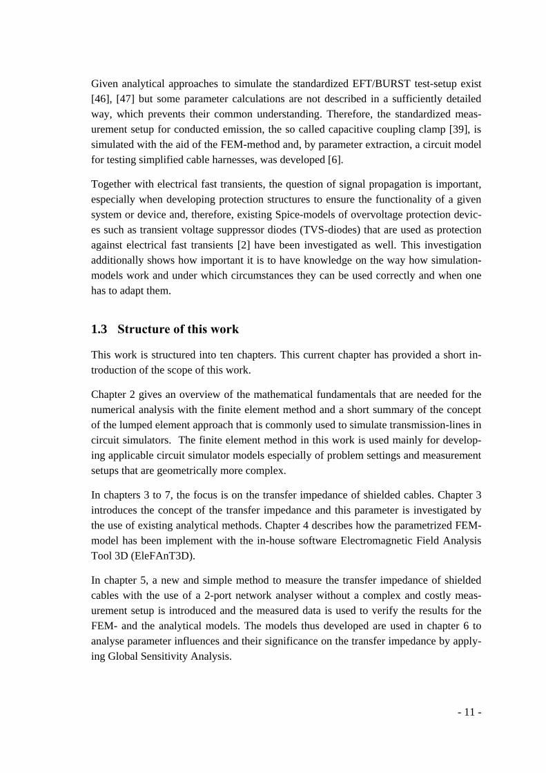
Fig. 3.5: Transfer impedance of a solid copper shield
Analytical model for the solid shield 3.4.1
The current distribution of the magnetic field inside a conductor is derived from Am-
pere’s law (2.11), and the constitutive relations (2.14) as
( ) ( ). H E (3.4)
Together with Faraday’s law of induction (2.13) and (2.14) this leads to the equation
2 j . H H (3.5)
For a straight cylindrical conductor with a given radius r this problem is solved with
the magnetic field, leading to Bessel’s equation
21( )rH H
r r r
(3.6)
with its solution
1 1( ) ( ).r B rAI KH (3.7)
The relation between the current and the magnetic field for this problem in cylindrical
coordinates is derived from (2.11) and is given as

- 34 -
1
( )zJ rHr r
(3.8)
again applying the constitutive relations from (2.14) and substituting the derivative of
(3.7) leads to
0 0[ ( ) ( )]z AI rE BK r
(3.9)
with j , 1( )I x and 1( )K x denote the first-order modified Bessel-functions of
the first and second kind and 0 ( )I x and 0 ( )K x denote the zero-order modified Bessel-
functions of the first and second kind.
A and B are constants, that are evaluated now for the solid shield with an inner radius
r a and an outer radius .r b
The current return path can be provided either inside or outside the shield which leads to
the surface impedances aaZ respectively bbZ (3.13) for the internal and the external
return. The impedance t ab baZ Z Z (3.14) denotes the transfer impedance from one
surface of the shield to the other [18], [19].
To derive the unknown constants A and B from (3.9), a known total current a bI I is
assumed, flowing in the solid cylindrical shield, where aI denotes the current of the
internal return and bI is the part of the current returning on the outside, as depicted in
Fig. 3.6.
Fig. 3.6: Definition of currents aI and bI for evaluation of the transfer impedance of a
solid shield

- 35 -
The current enclosed by the inner surface is aI and applying Ampere’s law (2.11), this
results in 2
aa
I
aH
. bI is the current enclosed by the outer surface, which analo-
gously leads to 2
bb
IH
b
.
Substituting aH and bH in (3.7), for the inner- and outer radius of the shield, gives
the following equations
1 1
1 1
( ) ( )2
( ) ( )2
a
b
Ia BK a
a
Ib B
AI
Ab
I K b
(3.10)
and the constants A and B can be derived as:
1 1
1 1
( ) ( )
2 2
( ) ( )
2 2
a b
a b
A I
B
K b I aI
aD bD
I b I aI
DI
aD b
(3.11)
where 1 1 1 1[ ( ) ( ) ( ) ( )]D I b K a I a K b .
Substituting (3.11) in (3.9) leads to
( )
( )
z aa a ab b
z bb b ba a
a I Z I
E
E Z
b Z I Z I
(3.12)
where aaZ is the surface impedance with the internal return and bbZ is the surface im-
pedance with external return and they are evaluated as:
0 1 0 1
0 1 0 1
1[ ( ) ( ) ( ) ( )]
2
1[ ( ) ( ) ( ) ( )]
2
aa
bb
Z
Z
jI a K b K a I b
aD
jI b K a K b I a
bD
(3.13)
and the transfer impedance tZ from one surface of the shield to the other is given as

- 36 -
1 1 1 1
1 1.
2 2 [ ( ) ( ) ( ) ( )]t ab baZ Z
abD ab I b K a I a KZ
b
(3.14)
Using the following approximation of the modified Bessel functions for the asymptotic
behaviour for small arguments 0 1nx :
2
1( )
( 1) 2
ln 02
( )( ) 2
02
n
n
n
xx
n
xn
x
x
I
n
Kn
(3.15)
(3.14) leads to the DC-resistance of the solid cable shield
1
( )( )dc
bR
a b a
(3.16)
and using the approximation of the modified Bessel functions for the asymptotic behav-
iour for large arguments 2 . |5| 0 2x n
1( )
2
( )2
xn
xn
I
K
x ex
x ex
(3.17)
(3.14) leads to the transfer impedance tZ of the solid shield
2 ( )
tab sin
Zh d
(3.18)
with d being ( )b a , i.e. the shield thickness.
3.5 Inductive region
In the case of braided shields, we can identify the DC-region and the skin effect losses
but at higher frequencies the inductive behaviour of the apertures of the shield is pre-
dominant and lead to a rise of the transfer impedance as depicted in Fig. 3.3.
- 37 -
The reason for this inductive behaviour is the so called aperture leakage that arises from
the geometry of the shield. The cable shield protects against external EMI fields and it
also protects against the leakage effects from the inner part of the cable. This shielding
effectiveness is reduced by the apertures in the shield. The resulting inductive behaviour
is strongly geometry dependent.
For this investigation, the problem setting is considered to be in the low-frequency do-
main, which means that the apertures are relatively small with respect to the wavelength
and therefore the geometry is electrically short [21].
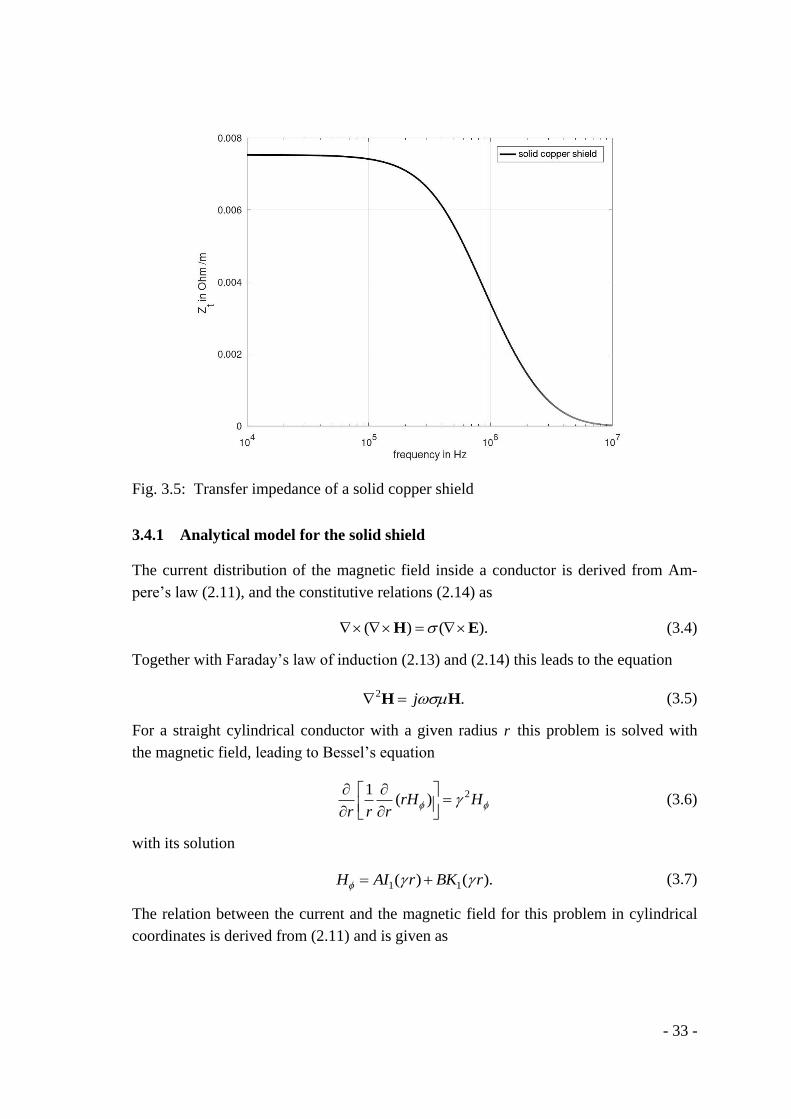
Analytical model for inductance calculation 3.5.1
To calculate the aperture leakage, an electric dipole source with its dipole moment ap
perpendicular to the aperture and a magnetic dipole source with its dipole moment am
in the aperture plane, located at the centre of the aperture, are assumed.
These dipole sources generate an electric-dipole field as well as a magnetic-dipole field.
According to [22], the first-order diffracted field by small apertures can be described as
the superposition of the two fields.
To obtain the dipole moments, the rhombic apertures of the shield are approximated via
elliptic apertures that are assumed to be in a conducting plane.
The magnetic dipole moment is then derived from the static magnetic dipole moment of
an ellipsoidal magnetic body that is placed in a uniform static magnetic field as depicted
in Fig. 3.7 on the right. The static magnetic dipole moment components can be calculat-
ed as
0
0( )
x x
x
mV
H
Lu
(3.19)
due to the field xH along the x - axis and
0
0( )
y y
y
mV
H
Lu
(3.20)
due to the field yH along the y - axis, as described in [24].

- 38 -
The electric dipole moment is derived from the static dipole moment of a dielectric
body that is placed in a uniform static electric field 0E along the z -axis, as depicted in
Fig. 3.7 on the left and the dipole moment zp is calculated as [24]:
0
0
00
)(
z
z
E
L
Vp
(3.21)
where V is the volume of the ellipsoid.
Fig. 3.7: Dielectric ellipsoid on the left and permeable magnetic ellipsoid on the right
The integrals for the constants nL are calculated by the aid of appropriate limiting pro-
cesses as in [23] and [24]:
2 2 2 2( ) ( ) )2 ( )(n
x y z
n
n x y z
ds
s s sL
s
(3.22)
for ,n x y and z and ,x y , z are the ellipsoid semi-axes.
Using (3.22), the static dipole moment then can be evaluated from (3.19) – (3.21) as

- 39 -
2
34
3 [ ( ) ( )]x x x
eH
Km
e E e
(3.23)
2 2
3
2
4 (1 )
3 ( ) (1 ) ( )y x y
e em H
E e e K e
(3.24)
3 2
0
4 (1 )
3 ( )
xz zp
eE
E e
(3.25)
where ( )K e and ( )E e are the complete elliptic integrals of the first and of the second
kind, respectively and
2
21 ,
y
x y
x
e (3.26)
defines the eccentricity of the elliptic aperture.
The effective dipole moments
1
4e m m m H (3.27)
0
1
4e e p p nnE (3.28)
result in the dyadic magnetic polarizabilities:
3 2
3 [ ( ) ( )]
xmx
e
K e E e
(3.29)
3 2 2
2
(1 )
3 ( ) (1 ) ( )
xmy
e e
E e e K e
(3.30)
0mxy myx (3.31)
and the electric polarizability
3 2
0
(1 ).
3 ( )
xe
e
E e
(3.32)
The effective aperture inductance of a single aperture can then be evaluated as:

- 40 -
0
2
0
2
,(2 )
(2 )
x mx
y my
L
rL
r
(3.33)
where r is the radius of the conducting tubular screen.
3.6 Applicable analytical model
The analytical approximation methods in general to describe the different regions of the
transfer impedance and their practical use have been studied in [26]-[30]. An overview
of those methods is also presented in [25]. The drawback of those models lies in the fact
that the results are mainly compared to measurements and therefore more excessive
geometry variations have not been studied in detail.
In the following sections the adjustment procedures for the applicable analytical model
are described. These adaptions are needed, since on the one hand, the coverage factor
has a direct influence on the DC-region respective the DC-resistance, which is not taken
into consideration for the solid shield in section 3.4.
On the other hand, the inductance calculation of the apertures by approximating the
rhombic shapes with ellipses, as it is done in section 3.5.1, leads to an overestimated
inductance value, which will be explained in section 3.6.2.
DC-region and skin effect losses 3.6.1
For calculating the DC-resistance including the skin-effect losses, the analytical ap-
proach of Schelkunoff [18] for solid cable shields, as mentioned before, provides very
accurate and stable results. Comparing the analytically derived values and the numerical
results shows that, to gather the correct DC-resistance, mainly the optical coverage fac-
tor of the given shield has to be taken into consideration additionally which leads to an
increase of the resistance value since the effective area for the current flow decreases.
In this case (3.14) leads to:
1 1 1 12 [ ( ) ( ) ( )
1
( ]
1
)t
opt ab I b K a I a K bZ
CF (3.34)
where the factor optCF describes the optical coverage of the cable shield.

- 41 -
Inductive region 3.6.2
As mentioned before, to calculate the aperture leakage the rhombic openings of the
braided cable shield are approximated via ellipsoids. Using the same length of the main-
and semi axis for this approximation leads to an overestimation of the calculated value.
To obtain better results, the magnetic polarizability can be written as in [31]-[34]
3
2m mS (3.35)
where S is the surface of the rhombic aperture, m is the magnetic polarizability from
(3.29) and (3.30) and m represents the dimensionless magnetic polarizability.
Using this representation, the dimensionless magnetic polarizabilities can be re-written
as
3
222
[ ( ) ( )]3 y
xmx
e
K e E e
(3.36)
for angles 45x
y
arctan
and
2
21 ,
y
x y
x
e which translates into weave
angles of 90 and
322
2
2
( ) (1 ) ( )3
y
my
x
e
E e e K e
(3.37)
for 45x
y
arctan
and 2
21 ,x
y x
y
e , which translates to weave angles
90 .
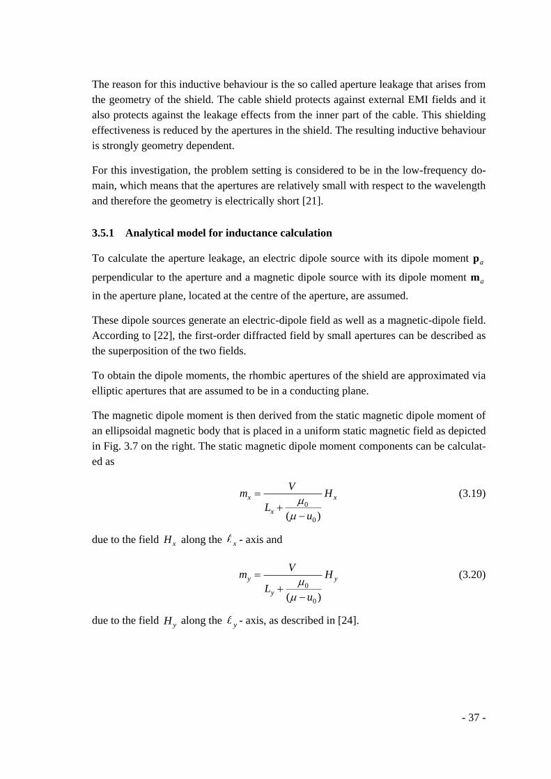
The two different cases for the weave angle are shown in Fig. 3.8.
- 42 -
Fig. 3.8: Approximation of rhombic apertures with ellipses
The effective aperture inductance of a single aperture is then evaluated similarly as in
(3.33):
0
2
0
2
(2 )
(2 )
x mx
y m y
L
L
b
b
(3.38)
where b is the outer radius of the shield taking the shield thickness respectively the
basic geometry into consideration.
The analytical results for these hole-inductance values are compared to results of the
FEM-model which will be explained in more detail in chapter 5.
The comparisons are depicted in Fig. 3.9 for weave angles 90 and in Fig. 3.10 for
angles 90 and the results stand in very good agreement.

- 43 -
Fig. 3.9: Comparison of hole inductance for weave angles 90 , FEM vs analytical
Fig. 3.10: Comparison of hole inductance for weave angles 90 , FEM vs analytical

- 44 -
Cable shield with multiple apertures 3.6.3
To gather the hole-inductance per unit length, the value in (3.38) has to be multiplied
with the number of apertures per meter of the cable shield [16].
Fig. 3.11: Definition of hole-distance for multiple apertures
For a cable shield with n apertures at an average distance D between the neighbouring
apertures as depicted in Fig. 3.11, the hole-inductance per unit length can be derived as:
1/
1/
xn
y
x
y
x
yn
L
L
L nL H mD
L nL H mD
(3.39)
A more detailed analysis on the influence of different parameters on the overall transfer
impedance is carried out in chapter 6 by the use of sensitivity analysis.

- 45 -
4 FEM model for transfer impedance of braided cable
shields
This chapter gives a short introduction of the software tool used and describes how the
FEM-model of the parametrized cable model has been implemented.
As mentioned before, the transfer impedance is not only frequency dependent, but ge-
ometry- and material parameters have strong influence on the shielding behaviour of a
given cable shield.
This chapter will take a closer look at the geometry dependencies with the help of the
finite element method. The advantages of numerical simulations are that these parame-
ter variations can be modelled exactly and they give a more precise evaluation model
for the analytical calculations. Even though the analytical model is verified by meas-
urements in section 5.3, based on the implemented FEM-model, more influences can be
investigated without the need to fabricate special cables and run extensive measure-
ments.
Using numerical simulations also gives the ability to investigate cable deformations
such as bending and stretching of the cable shield and the influence of the resulting ge-
ometry deviations on the shielding effectiveness.
For the FEM-model, the basic geometry parameters like diameter of the inner conduc-
tor, the distance from the inner conductor to the inner radius of the shield and the shield
thickness can be varied. For the cable shield, the weave angle and the coverage factor
are parametrized as well. This model works in the range of a coverage factor from 60%
to a full coverage of 100% which translates into a solid shield. These parameters should
suffice since coverage factors of 90% and higher are very common values for typical
coaxial cables.
As also mentioned before, the conductors of this cable are made of copper but this ma-
terial parameter can be varied for this model as well.
It has to be noted, that changing the basic geometry parameters like the distance from
the inner conductor to the outer radius of the shield are used to evaluate the influences
of these parameter variations on the shielding effectiveness. Changing these parameters
will lead to a change in the characteristic impedance of a coaxial cable as is mentioned
- 46 -
in section 3.2. The possible changes on the signal propagation properties, arising with
these parameter variations, are not under investigation in this work.
The reference model in this case is a standard RG58/CU coaxial cable, as mentioned in
chapter 3, which is used to verify the simulated results with measurements. A more de-
tailed description of the measurement setup and novelties of the same are discussed in
chapter 5.
For the numerical simulation, the A,V-A-formulation with current excitation is used, as
it is described in chapter 2, since for the evaluation of the transfer impedance, i.e. the
voltage on the outer side of the shield, a known EMI-current is needed, as seen in (3.1).
4.1 Space discretization using finite elements: EleFAnT3D
The software package Electromagnetic Field Analysis Tool (EleFAnT3D) [26] is used
to solve this three-dimensional electromagnetic problem.
The whole domain is divided into smaller subdomains, the so called finite elements,
over which simple basis functions are defined to approximate the solution. The software
package uses 2nd
order hexahedral elements that are defined via 20 nodes and 36 edges
and the unknown functions are represented on a nodal basis or on an edge basis.
In the case of node based elements the unknown scalar- and vector functions are ap-
proximated in the nodes that are associated with the element. Using continuous and
piecewise polynomial basis functions that satisfy
at node
at all other nod
1
e0 sj
jN
(4.1)
lead to the interpolated solution.
The basis functions can be expressed in terms of local coordinates ( ,, ) , that repre-
sent the position within the element. The global coordinates of the nodes ( ), ,j j jy zx
give the position within the global geometry and if the transformation between the glob-
al coordinates and the local coordinates is done with the same basis functions, the ele-
ments are so called isoparametric elements [35]. With this kind of representation, any
element in the global coordinate system can be transformed into a regularly shaped ele-
ment in the local coordinate system:
1 1 1
( , , ) ( , , ) ( , , )n n nn n n
j j j j j j
j j j
x x N y N z Ny z
(4.2)

- 47 -
where nn represents the number of nodes in the element and jN are the used shape
functions that depend on the number of nodes.
If vector quantities like vector potentials are considered, it is an advantage to approxi-
mate them with the aid of edge base functions since the nodal representation imposes
full continuity of the vector field in tangential and normal direction which can lead to
non-physical solutions [11]. Using edge based elements ensures the continuity of the
tangential component and allows the normal component to be discontinuous. The edge
basis functions are vectorial and satisfy
if
otherwise.
1
0iedge
i jd
jN r (4.3)
Applying (4.1) and (4.3) leads to sparse system matrices and the resulting linear equa-
tion system can be solved with direct or iterative procedures.
4.2 Cable shield model with EleFAnT3D
After this short introduction of the used software package, the following sections give a
description of how the fundamental geometry settings and the shield geometry was im-
plemented.
Basic geometry 4.2.1
The initial rectangular grid and the basic geometry is shown in Fig. 4.2, whereas the
rectangular grid elements are the macro elements which are divided into finite elements
as mentioned in section 4.1.

- 48 -
Fig. 4.2: Initial grid for 4x4 macro elements
The possibility to use so called “ellipses with stripes” is already implemented and this
special ellipsoid geometry is needed since the basic ellipsoid would eliminate macro
elements that are later needed to model the complex shield geometry. A comparison of
these two variants is shown in Fig. 4.3.
Fig. 4.3: Predefined variants for ellipses, on the right is the used geometry implementa-
tion providing macro elements for the shield geometry
The basic cable geometry consisting of the inner conductor and the cable shield is
shown in in Fig. 4.4.

- 49 -
Fig. 4.4: Top view of quarter model and full cable model for solid shield
The implemented shield consists of two macro-elements in the x - y plane where the
middle radius varies with the frequency due to skin effect. This frequency dependent
behaviour is also applied to the model of the inner conductor, in case a termination re-
sistance is needed for application purposes.
Shield geometry 4.2.2
As mentioned before, for the cable model, the implemented ellipsoids with stripes as
depicted in Fig. 4.3 are used to achieve a sufficient number of macro-elements to model
the rhomboid shaped apertures for the cable shield.
There are two main models, one for a coverage factor of 75% and higher and one for a
coverage factor below 75% . The modelling of the apertures especially modifying the z
- layers for these two cases is explained later on.
First, the joint base-manipulations are explained.
Due to the use of the ellipsoids, some macro-elements are eliminated and cannot be ma-
nipulated, as shown in Fig. 4.5, and this needs to be considered for later geometry calcu-
lations since these eliminated elements determine the minimal possible coverage factor
and the limitation of the basic geometry.

- 50 -
Fig. 4.5: Basic geometry indicating eliminated macro elements
Nevertheless, the implemented model can vary the coverage factor from 60% to 100%
and also the weave angle can be arbitrarily set up to 179 degrees. These very extreme
variations are more for evaluation purposes or for the investigation of pinched, stretched
or bent cables since a common coaxial cable usually has a coverage factor between
95% and 98% and a weave angle of around 30 degrees.
To achieve the desired geometry, the elements considered for the conductive material
and the elements for the apertures are chosen from the beginning and remain the same
for any parameter-variation of the implemented shield geometry.
Material parameters can be set directly and the parameterization of the main geometry
can be done by modifying the x - and y - distances of the main grid.
For the apertures, geometry parameters like the radius of the shield and shield thickness
together with the coverage factor or optical coverage factor ( cf ) and the weave angle
are needed. This data usually can be taken from datasheets and the weave angle can
be measured. A model with a coverage factor of 98% is shown in Fig. 4.6.

- 51 -
Fig. 4.6: Sample cable model for coverage factor of 98%
For the aperture size, a so called shielding-factor ( sf ) is introduced. This factor de-
scribes the ratio of the shield-material versus the aperture opening in the x y plane.
The used procedure herein is:
The area of a certain cylinder based on the outer shield circumference ( outeru ) and the
angle as depicted in Fig. 4.7, where is the complementary angle of half of the
weave angle , is derived as
90 .2
(4.4)
To calculate the aperture area, the area of the solid cylinder jacket is multiplied with the
coverage factor and subtracted from the full area
2· 1apertures outer cylinderuA h cf (4.5)
giving the area of all apertures on the cylinder jacket. To derive the area of one single
aperture, the area has to be divided by four as in Fig. 4.7.

- 52 -
Fig. 4.7: Derivation of the shielding-factor for a given optical coverage
Since for the FEM-model the coordinates are calculated for an eighth of the cable cir-
cumference, this leads to the working area A as in Fig. 4.7
2 2
1/8 1/8(1 ) (1 ) tan
16 2 2
apertures apertureA u sf h u sfA
(4.6)
where 1/8u is one eight of the outer shield circumference.
The shielding-factor then can be derived as
21/8
12
.tan
A
usf
(4.7)
This shielding-factor is a constant parameter for one given geometry-model and the
shielding material component is calculated as:
/8
2n
nmat n
n
u sfss inr
r
(4.8)

- 53 -
and the non-material regions are calculated as
/8 (1 )
2n
nvoid n
n
u cfsins
rr
(4.9)
where nr and /8nu denote the n radii and circumferences of the macro-elements the
shield is modelled as depicted in Fig. 4.8.
Fig. 4.8: Quarter model of cable shield indicating the material- and non-material re-
gions of the shield
In Fig. 4.8, the total range of the material- and non-material parts from (4.8) and (4.9)
are indicated as nxs and nys in green and the x -and y - values of the macro elements
for modifying the regions with shielding material along the y - and the x - axis, respec-
tively, are depicted in red and for modifying the regions without shielding material are
depicted in blue. The macro- elements of the shield for modelling the braid are coloured
in orange and the elements for modelling the holes are white.

- 54 -
Fig. 4.9 shows the order of how to modify the x - intervals on the y - axis and vice ver-
sa, depending on which octant is modified.
Fig. 4.9: Manipulation in the x-y plane
Now the elements on consecutive z - planes can be modified with respect to these val-
ues and the aforementioned eliminated macro-elements have to be considered carefully
to avoid any intersections between single elements or too heavy geometry distortions.
This z - layer manipulation is now divided into the two main geometry models.
Modelling the coverage factor of the shield 4.2.3
In the previous section, the manipulations in the x - y plane have been explained. To
implement a desired coverage factor, these manipulations have been done on consecu-
tive z -layers to obtain the final geometry. The implementation is divided into two dif-
ferent models, one to implement coverage factors of 75% and higher and one to im-
plement coverage factors below 75% . The difference between these two models is ex-
plained in the following subsections.

- 55 -
4.2.3.1 Coverage factor of 75% and higher
In this case, three different z -layers have to be modified and consecutively repeated to
model the braided pattern as shown in Fig. 4.10.
Fig. 4.10: Different layers for cable model with coverage factor of 75% and higher
For the geometry variations with a given coverage factor of 75% and higher, the first
and the third z -layer have half of the material thickness, as it is depicted in Fig. 4.10 as
well.
Layer 1 and Layer 3 always have half of the material thickness ( / 2sf ) so a constant
shield-material coverage can be achieved which is due to the assembly of the braid pat-
tern. The height of the z -layers as depicted in Fig. 4.10 are calculated as
1
( )2
outeraperture
u(1- cf) tan
8h z = (4.10)
In this case, the absolute height of one element ( cylinderh ) with respect to the shield radi-
us and weave angle, as shown in Fig. 4.6, is not kept constant. With this approach, it is
possible to model cable deformations such as compressed or stretched cables as depict-
ed in Fig. 4.11.

- 56 -
Fig. 4.11: Example for possible cable variations by changing the coverage factor by
altering the size of the apertures
Adding an additional z -layer after the second allows to change the coverage factor not
only by the size of the apertures by changing the shield factor but by varying the num-
ber of apertures per length, as it is depicted in Fig. 4.6 and Fig. 4.12.
Fig. 4.12: Example for possible cable variations by changing the coverage factor by the
number of apertures per length
4.2.3.2 Coverage factor less than 75%
An example for coverage factors of less than 75% is shown in Fig. 4.13. In this case
four different z -layers have to be taken into account

- 57 -
Fig. 4.13: Shield model with coverage factor of 60%
Again, Layer 1 and Layer 4 have half of the material thickness which is again due to the
assembly of the braid pattern to achieve a constant shielding material thickness as de-
picted in Fig. 4.14.
Fig. 4.14: Different layers for cable model with coverage factor less than 75%
The height of the z -layers to get the correct rhomboid shape is depicted in Fig. 4.15 and
the calculation of the heights is done as:

- 58 -
1 2
1
2 1
10.5 ( )
2
0.5 ( )
1z z
2
outeraperture
outer
aperture
uz (1- cf ) tan
8
uz = (cf ) tan
8
h = z
h
(4.11)
Fig. 4.15: Calculation of height of z-layers
Again, varying coverage factors and cable deformations can be modelled with this ver-
sion as well and some examples for this shield geometry model are depicted in Fig.
4.16.
Fig. 4.16: Examples for possible cable variations

- 59 -
5 Measurement technique
This chapter describes a new and reliable measurement method for the transfer imped-
ance with the help of a 2-port network analyser that is fast and very simple to imple-
ment. This method was first presented in [8] and [9].
Known techniques to measure the transfer impedance are usually very costly and time
consuming because of the complex measurement setup [35].
Nevertheless, it is noteworthy that this method developed by us is not a standardized
one but it can be easily applied for quality control of given coaxial cables or for investi-
gation of cable behaviour after exposing the cable under test to mechanical or thermal
stress since frequent measurements can be done rather quickly.
5.1 Measurement setup
The needed parameters to derive the transfer impedance are the scattering-parameters
(s-parameters) 11S and 21S as they are depicted in Fig. 5.1 and, therefore, the measure-
ment is done with a 2-port network analyser and the transfer impedance tZ is then eval-
uated as
1
' /t
shield
Z U mI
(5.1)
where shieldI denotes the current through the shield and 'U describes the voltage drop
along the outer side of the shield as described in section 3.3.
The two ports Port 1 and Port 2 of the network analyser are denoted as 1P and 2P ,
respectively in Fig. 5.1 and 0Z represent the input and output impedance. With the aid
of a so called adapter, as shown in Fig. 5.2 on the right, where the inner conductor is
basically soldered to the shield, the shield of the cable under test is connected to the
inner conductor without being connected to the ground terminal of Port 1 of the network
analyser.

- 60 -
Fig. 5.1: Model circuit [8], © 2017 IEEE
The parameters iR and iL model the inner conductor and the parameters sR and sL are
used to model the shield of the cable. The ground terminals of the two ports of the net-
work analyser cannot be referenced to the same ground potential and therefore gR and
gL stand here for the internal ground link. Additionally, different ground symbols were
used to distinguish the two different ground potentials of the ports, which can be rea-
soned by the physical design of the network analyser.
Fig. 5.2: Test setup [8], © 2017 IEEE
The representation of the setup as lumped elements is again valid as long as the length
is considered to be electrically short and the rule of the maximum length 10
is ful-
filled as discussed in Section 2.4.
Since exported measured values are given in logarithmic format, the s-parameters have
to be converted to linear scale

- 61 -
( )
2010xS dB
xlinS (5.2)
where xS denotes the magnitudes of the parameters 11S and 21S .
5.2 Parameter evaluation
The aforementioned setup describes a passive two-port network with a system imped-
ance 0Z of 50 on both Port 1 and Port 2. Port 1 leads into a low impedance path of
the shield consisting of sR and sL and the ground impedance gR and gL to get a
closed loop. The inner conductor with the impedance iR and iL of the unmodified end
of the cable under test is terminated at Port 2 of the network analyser by the impedance
0Z . Since it is assumed that the characteristic impedance of 50 is several orders of
magnitude greater than the shield impedance and the ground impedance
0( )s gZ ZZ , the output current of Port 1 will take the current path denoted as
“loop” in Fig. 5.1. The needed reflection coefficient 11S is defined as the ratio between
the voltage out of Port 1 and the reflected voltage at Port 1 and is given as
111
1
.out
in
Su
u (5.3)
The power ratio 1inP at Port 1 can be expressed in terms of the 11S parameter as
21 11(1 | | )in genPP S (5.4)
where genP denotes the output power at Port 1 of the network analyser.
The input impedance of Port 1 can be calculated via the 11S parameter as well, and it is
given as
1111 0
11
1
1 SZ
SZ
(5.5)
and together with (5.3) the shield current shieldI can be derived as
1
11
.inshield
P
ZI (5.6)
Having now computed the shield the current shieldI for (5.1), the voltage drop along the
cable under test has to be evaluated by the use of the reflection coefficient 21S .

- 62 -
The power experienced at Port 2 is only a fraction of the transferred power 1inP due to
the fact that, in this setup, the ground connectors of the ports are separated by the
ground impedance gR and gL . The voltage at Port 2 can now be evaluated as
2 21 1 0inU S P Z (5.7)
and (5.1) leads to
2
1't
shield
Z UI
(5.8)
where 2'U is the referenced voltage to a unit-length of 1m.
With the measured parameter 21S the transfer impedance can now be written as
110 21
11
1 1/ .
1tZ
SZ S m
S l
(5.9)
Considering (5.9), it is evident that different kinds of cables under test can be evaluated
with this method, since the intrinsic and unknown impedances have no direct influence
in the evaluation of the transfer impedance and the only parameters needed are the re-
flection coefficient 11S , the forward gain coefficient 21S and the system impedance of
the given setup.
An equivalent circuit of the transfer impedance with respect to this given setup is shown
in Fig. 5.3.
Fig.: 5.3: Equivalent circuit for braided cable shields [8], © 2017 IEEE

- 63 -
The transfer impedance tZ in this equivalent circuit consists of the impedance iZ and
sZ , where the shield impedance is split into an inner system ( siZ ) and an outer system
( SoZ ). It is noteworthy that the system impedance 0Z is purely resistive, whereas
,So SiZ Z and iZ are complex values.
5.3 Results and comparison with analytical and numerical models
The measurements have been carried out for cables under test of different lengths but of
the same cable model. It has also been proven that the cable layout for this measurement
setup is not of importance and even having a loop for longer cable length does not in-
fluence the measured results. This is shown in Fig. 5.4 for a measured cable under test
for 1m of length. The reason for this behaviour is that even if there is a small rise in the
impedance sZ , the current will drop accordingly and this will lead to a relative voltage
drop for 2U at Port 2 and therefore this influence is cancelled out.
The same stability was seen when a metallic plate was put under the cable under test.
However, this condition does not hold in case of propagation effects as for example
when resonances occur.
Fig. 5.4: Influence on loops in the setup on transfer impedance [8], © 2017 IEEE
Fig. 5.5 depicts the comparison between the measured results and the numerical and
analytical model for the transfer impedance. The cable under test in this case was the
standard RG-58 coaxial cable with a characteristic impedance of 50 .

- 64 -
Fig. 5.5: Comparison of measured and simulated data [8], © 2017 IEEE
The results stand in very good agreement and this comparison was also used to validate
the numerical and analytical models discussed in the previous sections.

- 65 -
6 Parameter dependencies for transfer impedance
The aim of this chapter is to give a short overview of the influence of parameter varia-
tions on the transfer impedance, geometry- as well as material-related. At first the inves-
tigation includes the influence of the shield thickness and the used material to cover the
basic shield variations. The second part covers the geometry variants of the braided
shield affecting the aperture geometry including influential parameters as coverage fac-
tor and weave angle, altering the size of the area of a given aperture and the last part is a
combination of these variations to demonstrate the overall influence.
The basic analysis in sections 6.1-6.3 has been done with the FEM-model described in
chapter 4. Since the numerical and analytical results always stood in very good agree-
ment, a more detailed parameter analysis using sensitivity analysis with the aid of the
analytical model has been carried out in section 6.4 to save computational time.
6.1 Basic shield parameters
Fig. 6.1 demonstrates the influence of the shield thickness on the low frequency range
determining the DC- resistance value and the skin effect losses for increasing frequen-
cies in case of a solid shield.
The most dominant effect at first sight is the influence of the shield thickness on the
DC-resistance, since the DC-resistance is directly influenced by the current carrying
cross-section of the conductor which is determined for low frequencies by the shield
thickness:
1
( )( )dc
bR
a b a
(6.1)
where a denotes the inner radius of the shield, b the outer radius and is the conduc-
tivity of the shielding material as it is mentioned in section 3.4.
Not only the value of the DC-resistance is affected by the shield thickness, but also the
beginning of the region defining the skin effect losses, as seen in Fig. 6.2. To make this
effect clearer, the curves are normalized with respect to the DC-resistance value.

- 66 -
The corner frequency at which the decrease of the transfer impedance of the solid shield
starts can be coarsely approximated as the frequency when the skin depth equals the
shield thickness d , i.e.
2
0
1cf
d
(6.2)
where again is the conductivity of the shield and 0 denotes the permeability of free
space.
Fig. 6.1: Influence of shield thickness and frequency behaviour

- 67 -
Fig. 6.2: Influence of shield thickness and frequency behaviour normalized by dcR
Therefore, a thicker shield in general translates into a better shielding effectiveness at
lower frequencies.
Looking at (6.1) and (6.2), it also clear that the conductivity of the shield material has
an impact on the DC-resistance and the frequency dependent skin effect losses as well.
For this evaluation, the used conductivities are copper ( 7 15,8 10 ( )m ), gold (
7 14,5 10 ( )m ) and aluminium ( 7 13,7 10 ( )m ).
Fig. 6.3 compares the transfer impedance of a solid shield with a given shield thickness
of 0.2mm with respect to different materials. Here the DC- resistance alterations are
clearly visible. Fig. 6.4 again depicts the normalized curves to represent the frequency
dependence of the skin effect losses and the aforementioned frequency cf more clearly.

- 68 -
Fig. 6.3: Transfer impedance for different shield conductivities
Fig. 6.4: Transfer impedance for different shield conductivities normalized to dcR

- 69 -
6.2 Coverage factor and weave angle
This section gives a short overview on the influence of the geometry variations regard-
ing the optical coverage factor of a cable shield and different shapes of the rhombic ap-
ertures.
Fig. 6.5 depicts the graph of the transfer impedance of a cable shield with a constant
thickness of 0.2mm and a given weave angle of 30 degrees but with varying coverage
factors, changing the size of the apertures without altering the shape. A higher coverage
factor translates into less or smaller apertures and this leads to a smaller hole-inductance
resulting in a better shielding effectiveness. It is also noteworthy that the coverage fac-
tor has an influence on the DC-resistance value too, since a decreasing coverage factor
leads to a decreasing effective conductor area which translates into a higher resistance
value as seen in (3.34).
Fig. 6.5: Influence of coverage factor on transfer impedance
Fig. 6.6 shows the transfer impedance for a constant coverage factor of 95% but for
varying weave angles comparable to stretching or compressing a cable with a length of
one meter. In this scenario, the transfer impedance remains more or less the same. The
explanation for this behaviour is that the height of one single aperture varies with re-
spect to the changing angle. In case of a smaller weave angle, the height of every single
aperture is elongated which leads to a higher inductance value but is also leads to fewer

- 70 -
apertures per meter of a given cable and the two effects seem to keep balance. The same
is valid for increasing weave angles, since the height of one aperture is compressed,
decreasing the inductance of one single aperture but increasing the number of apertures
per meter. It has to be mentioned that, in this case, the reference length of the cable is of
importance, since it is crucial whether the inductance changes based on the deformities
are eliminated or not.
Fig. 6.6: Influence of different aperture shapes with constant reference cable-length
6.3 Overall influence
After the basic alterations have been discussed, a variation of all parameters is briefly
demonstrated here. Fig. 6.7 shows the transfer impedance for constant coverage factor
and weave angle but with different shield thicknesses. As already mentioned, the influ-
ence on the DC-resistance and the frequency curve in the lower frequency spectrum is
visible but, also in the higher frequency range, a difference is noticeable. Indeed, a shift
of the curve with respect to the frequency can be seen here. It is clearly visible that, for
evaluation and modelling of the transfer impedance, the shield thickness is a highly im-
portant parameter and deviations in its dimensions lead to a substantial change.
Another factor is the influence of the number of apertures due to a given layout, as de-
picted in Fig. 6.8.

- 71 -
Fig. 6.9 contrasts the impedance curves of these two model variants and shows the in-
fluence of a given cable layout with apertures of the same size and shape but different
numbers per meter. Reducing the number of holes in the shield is another way to in-
crease the coverage factor.
Fig. 6.7: Comparison of different shield thicknesses on overall behaviour
Fig. 6.8: Different layout versions determining the number of apertures per length
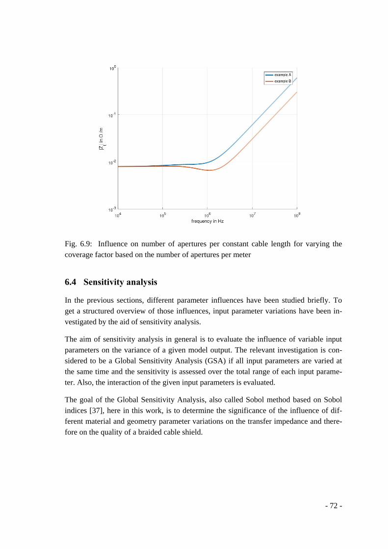
- 72 -
Fig. 6.9: Influence on number of apertures per constant cable length for varying the
coverage factor based on the number of apertures per meter
6.4 Sensitivity analysis
In the previous sections, different parameter influences have been studied briefly. To
get a structured overview of those influences, input parameter variations have been in-
vestigated by the aid of sensitivity analysis.
The aim of sensitivity analysis in general is to evaluate the influence of variable input
parameters on the variance of a given model output. The relevant investigation is con-
sidered to be a Global Sensitivity Analysis (GSA) if all input parameters are varied at
the same time and the sensitivity is assessed over the total range of each input parame-
ter. Also, the interaction of the given input parameters is evaluated.
The goal of the Global Sensitivity Analysis, also called Sobol method based on Sobol
indices [37], here in this work, is to determine the significance of the influence of dif-
ferent material and geometry parameter variations on the transfer impedance and there-
fore on the quality of a braided cable shield.

- 73 -
The model considered for this analysis is given as
1(x )ny f x (6.3)
where y denotes the output (in our case the transfer impedance) and the variables
1 nx x are the independent input parameters.
The information whether a random input variable ix is influential on the investigated
output or not is given by the first Sobol index. It gives the contribution of the random
variable ix to the change of the model output without taking interactions with other
input variables into consideration.
The input variable is considered to be influential if the conditional variance [ ]iV(E y | x )
is large compared to the variance of the quantity of interest ( )V y and therefore the first
Sobol index is defined as:
( [ | ])
( ) ( )
i ii
V V E y x
V y V yS (6.4)
where [ ]iE y | x is the expected value of the model output y with a fixed parameter ix .
To gather information regarding the sensitivity of first order effects and regarding the
interaction between one input parameter and all the other parameters, the total Sobol
index or total-order sensitivity index is evaluated as
~( [ | ])1 .
( )
iTi
V E y
VS
y
x (6.5)
where ~ix denotes all variable input parameters except ix .
The second Sobol index gives the influence on the output by the interaction of input
parameters ix and jx and it is defined as:
( ( | , )) ( ( | )) ( ( | ))
.( ) ( )
ij i j i j
ij
V V E Y x x VS
E Y x V E Y x
V Y V Y
(6.6)
For the investigation of the transfer impedance only first-order, total-order and second-
order indices defined in (6.4)-(6.6) have been evaluated.

- 74 -
Sensitivity analysis for transfer impedance 6.4.1
The investigated parameters for this analysis are:
Variable Input Parameter
1x … shield thickness
2x … coverage factor
3x … conductivity of the shield
4x … inner radius of the shield
5x … weave angle
6x … number of apertures per meter
The sensitivity analysis has been carried out for different frequency points at
10kHz, 100kHz, 1MHz, 10MHz and 100MHz . The results are depicted in Fig. 6.10.

- 75 -
Fig. 6.10: Results for GSA: first-order, total-order and second-order indices

- 76 -
6.5 Results
It is evident from the results that the parameter influences vary considerably for differ-
ent frequency ranges.
For lower frequencies, the most influential parameters are the basic geometrical dimen-
sions and material properties like shield thickness, conductivity and the inner radius of
the shield, which have a direct influence on the DC-resistance and the skin effect losses.
The influence of the coverage factor can be considered to be minor. The frequency
where the skin effect losses start to dominate can be roughly estimated as the frequency
for which the skin depth equals the shield thickness, hence this is highly dependent on
the conductivity value and the basic geometry of the cable.
The influence changes for higher frequencies in the inductive region, where the most
influential parameters are the coverage factor and the number of apertures (changing the
latter is also a way to alter the coverage factor).
6.6 Conclusion
Even though just the most common parameter variations have been demonstrated here,
it is clear that small changes in the model can significantly alter the transfer impedance.
For evaluating the outcome of altered weave angles, it is of great importance whether
the evaluation is executed for a constant cable length or the alterations are assumed to
change the length of the cable as well varying the number of the apertures of the cable
under test.
Since the possible parameter variations are very extensive, it is of great importance to
design the simulation model as exactly as possible to get reliable results and to be able
to match the simulated outcome with real world behaviour.
In the author’s opinion, the transfer impedance can be simulated fairly accurately for a
very precise and specified setup and it is a suitable quantity for cable characterizations.
However, it has been demonstrated that parameter variations are highly influential and it
should be kept in mind that, in real-world applications, all possible parameter influences
demand a very accurate knowledge of the given test-setup.

- 77 -
7 Circuit Model
This chapter describes the implementation of a circuit model to simulate the transfer
impedance in any circuit simulator as, for example, LTspice used in this work.
At first, a model to simulate the skin effect losses of a cable shield is proposed which
ultimately is the more challenging part since the aperture leakage then can be imple-
mented by a series inductance (7.1) and the desired transfer impedance is represented by
a series connection of the impedances representing skin effect losses and the hole in-
ductance of all apertures:
t s aZ LZ j (7.1)
where the term sZ represents the DC-resistance and for increasing frequencies the oc-
curring skin effect losses and aL characterises the inductive behaviour of the shield
apertures.
7.1 Modeling skin effect losses
To model the skin effect losses, voltage dependent voltage sources provided by LTspice
are used. A voltage dependent source, it can be either a voltage or current source, de-
couples the single stages of the ladder-network from one another so each single stage
remain uninfluenced by the stages before or after.
An exemplary circuit model of four stages is depicted in Fig. 7.1.
Fig. 7.1: Circuit model for skin effect losses in LTspice

- 78 -
The first stage is used to fix the DC-resistance dcR . The current of the current source is
set to 1 Ampere as it is also done with the FEM-model and the measurement setup. Note
that, for this variant, the inductance values are kept at a constant value of 1nH and the
gain of the dependent voltage sources is kept at constant factor of 1 since it is visible in
(7.5) that there is no gain-factor due to the single stages in the magnitude.
The resistance 1R for the second stage is determined as
1 2workfR L (7.2)
where workf is the frequency when the phase of the transfer impedance of the solid
shield is at 90 degrees and this frequency point can be obtained as
10
work cf fe
(7.3)
Furthermore, cf is again the corner frequency at which the skin depth equals the shield
thickness as mentioned in as mentioned in section 6.1 and it is derived as
2
1c
df
(7.4)
where d denotes the shield thickness.
If only the magnitude of the transfer impedance is available, cf is also the frequency
point at which the magnitude of the transfer impedance is decreased by the factor 1
e.
The other resistance values 2 nR R can be approximated with 1R n where n is the
number of stages of the ladder network.
The voltages of the single stages of the network can then be calculated as:

- 79 -
0 0
1 0
1
2 1
2
1
1
1
1
1
1
1n n
n
U
UL
R
L
R
I R
U
j
U U
j
LU U
jR
(7.5)
Fig. 7.2 shows the magnitude and phase of the simulated results for a shield thickness of
0.5mm for a solid copper shield for a four-ladder network compared to the analytical
solution.
Fig. 7.2: four-ladder network vs analytical model for solid copper shield of 0.5mm
thickness
It is noteworthy that the curve shape of the magnitude can be derived even with a two-
ladder network, the phase can be approximated for the desired frequency range by in-
creasing the stages if needed. Fig. 7.3 depicts again magnitude and phase of the same
solid shield approximated via an eight-ladder network.

- 80 -
Fig. 7.3: eight-ladder network vs analytical model for solid copper shield of 0.5mm
thickness
Fig. 7.4 shows again a four-ladder network simulation compared to the analytical curve
for a shield thickness of 0.1mm to demonstrate that this very simple design process is
valid for different shield geometries as well.
Fig. 7.4: four-ladder network vs analytical model for solid copper shield of 0.1mm
thickness
The resistance values of this model are in the mΩ range and therefore it is important to
understand the circuit analyser tool as well. In general, inductances in LTspice have
some implemented serial resistance to avoid singularities. For the inductance, a default
serial resistance of 1mΩ is pre-set. To deal with this parasitic behaviour, there are some
alternatives: It is possible to set the parasitic value to zero and develop the model as in
(7.5) or, as an example, take the parasitic behaviour into consideration.

- 81 -
In the second case, the voltages of the single stages are calculated as in (7.6) noting that,
due to the parasitic resistance parR , the gain of the output voltage has to be corrected.
This can be done by dividing the final result by the overall gain of the circuit or by ad-
justing the gain-values of the single stages of the circuit respectively.
0 0
11 0
1
1
22 1
2
2
1
1
)1
1
(
( )
(
( )
(
)1
1)
)
(
1
par
par
par
par
nn n
n par
n par
I R
UR
j
U UR
j
U
U
RU
LR
R R
R
LR
UR
j
R R
R
LR
R R
(7.6)
Another possibility is to choose a different inductance value to increase the resistance
values and, as a consequence, reduce the relative influence of the error of the parasitic
resistance parR . Nevertheless, it is always important to fully understand the implement-
ed simulation models and parameters.
To demonstrate that this circuit model is valid for arbitrary shield thicknesses and mate-
rial properties, the simulated results are compared to the analytical results and this is
depicted in Fig. 7.5 and Fig. 7.6.
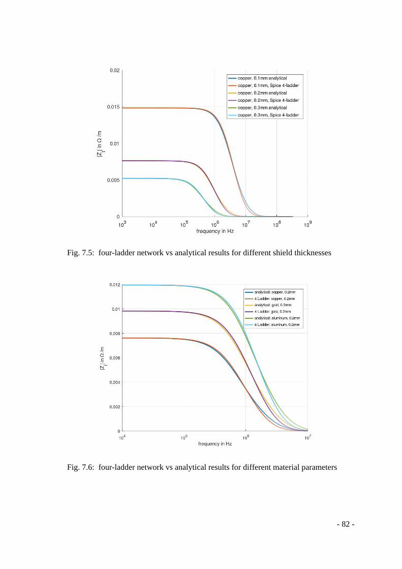
- 82 -
Fig. 7.5: four-ladder network vs analytical results for different shield thicknesses
Fig. 7.6: four-ladder network vs analytical results for different material parameters

- 83 -
7.2 Transfer impedance of braided shield
As mentioned in the beginning of this chapter the overall transfer impedance can be
simulated as a simple series connection of the DC-resistance and the skin-effect losses,
which are both modelled via the circuit model in Fig. 7.1 and the inductance determined
by aperture leakage of the shield as in (7.1). The inductance values can be derived ana-
lytically, as described in chapter 3 or with the aid of numerical simulation with the finite
element model as in chapter 4.
Fig. 7.7 compares the results of the numerical model and the circuit model simulated in
LTspice and everything stands in very good agreement.
Fig. 7.7: results for numerical simulation and circuit model in LTspice

- 84 -
8 Investigation of spice models for transient voltage
suppressor diodes
While the preceding chapters dealt with the broader theory behind the transfer imped-
ance and FEM-based analytics, this chapter deals with the specific case of transient
voltage suppressor diodes based on my publication [2].
Transient voltage suppressor (TVS)-diodes are commonly used devices for overvoltage
protection against electrical fast transients (EFT/BURST) and electrostatic discharge
(ESD) and act as a clamping device for overvoltage peaks. The investigation of these
protective measures is an important topic in terms of signal integrity and immunity as
well to ensure the correct functionality of subsequent devices.
This investigation is not dominantly focused on the response behaviour of the TVS-
diode but on the transient disturbances that are generated by the device itself.
Since these diodes are very common, models are largely available in circuit simulation
tools as for example LTspice used in this work.
Concerning the disturbances that are generated by these devices, certain implemented
diode- model types can present inaccuracies for this kind of prediction, especially in the
cut-off region, which is presumably due to the fact that the model of the implemented
junction capacitance follows a linear extrapolation and this leads to differences between
the simulated results and the real measured behaviour of the device under test.
For the simulation of this problem setting the measurement setup is considered as a
transmission-line and can be simulated in LTspice via the lumped-circuit approach as
described in Chapter 2.
8.1 Electrical Fast Transients
The investigated transient phenomena here are electrostatic discharge (ESD) and elec-
trical fast transients (EFT/BURST) as they are described and standardized in [38] and
[39].
These waveforms’ characteristics are a relatively fast rise time which leads to disturb-
ances at very high frequencies and both of these test cases constitute an important sub-

- 85 -
set of investigations in the field of electromagnetic compatibility in terms of conducted
emission, especially immunity.
Electrostatic Discharge - ESD 8.1.1
This pulse is characterized by its very fast rise- and fall-time of its first peak (“initial
peak”). Rise-time rt and fall-time ft are both within the range of 0.7ns to 1ns and are
measured from 10% to 90% of the maximum peak value. The typical pulse shape is
depicted in Fig. 8.1. This particular characteristic used here meets the requirements of
the system level ESD as characterized in [38].
Fig. 8.1: Waveform: ESD-pulse [2], © 2019 IEEE
Nominal peak values of this pulse can range from 500V up to 4kV. Another character-
istic for this pulse is its high current level but, due to the fact that this pulse is fairly
short, the main disturbances are generated as a result of its fast timing characteristic
generating disturbances at very high frequencies rather than in terms of high energy
levels.
EFT/BURST 8.1.2
This pulse is characterized by its rise-time and its pulse width as standardized in [39].
The rise- time is nominally between 3.5ns and 6.5ns and the pulse- width should be in
the range of 35ns to 65ns . The waveform can be analytically modelled via a double
exponential pulse as
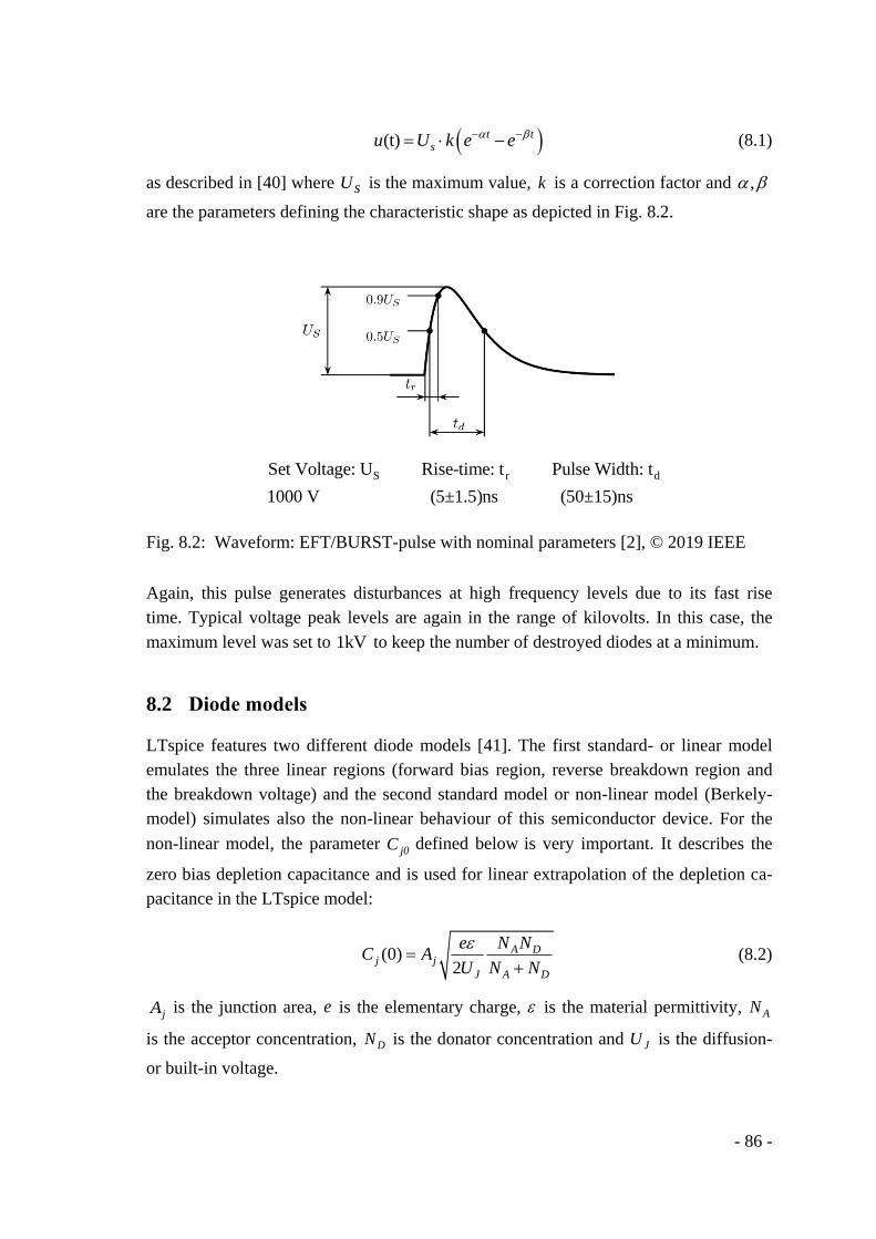
- 86 -
(t) t tsU k e eu (8.1)
as described in [40] where sU is the maximum value, k is a correction factor and ,
are the parameters defining the characteristic shape as depicted in Fig. 8.2.
S r dSet Voltage: U Rise-time: t Pulse Width: t
1000 V 5±1.5 ns
50±( ) ( 15)ns
Fig. 8.2: Waveform: EFT/BURST-pulse with nominal parameters [2], © 2019 IEEE
Again, this pulse generates disturbances at high frequency levels due to its fast rise
time. Typical voltage peak levels are again in the range of kilovolts. In this case, the
maximum level was set to 1kV to keep the number of destroyed diodes at a minimum.
8.2 Diode models
LTspice features two different diode models [41]. The first standard- or linear model
emulates the three linear regions (forward bias region, reverse breakdown region and
the breakdown voltage) and the second standard model or non-linear model (Berkely-
model) simulates also the non-linear behaviour of this semiconductor device. For the
non-linear model, the parameter j0C defined below is very important. It describes the
zero bias depletion capacitance and is used for linear extrapolation of the depletion ca-
pacitance in the LTspice model:
(0)2
A Dj j
J A D
N NeA
UC
N N
(8.2)
jA is the junction area, e is the elementary charge, is the material permittivity, AN
is the acceptor concentration, DN is the donator concentration and JU is the diffusion-
or built-in voltage.

- 87 -
The depletion capacitance as described in [41] and [42] is derived as
(0) 1 1
( )2 3
1
j
j m
J
U
U
CC U m
(8.3)
Fig. 8.3 shows the capacitance as a function of the forward voltage and compares the
extrapolated value used in LTspice and the real curve characteristic.
Fig. 8.3: Depletion capacitance in relation to the forward voltage (real behaviour vs
non-linear model) [2], © 2019 IEEE
Comparison of the models 8.2.1
Before starting the comparison of the implemented models, it has to be mentioned that
no model is either better or correct or wrong. In the course of this investigation, it will
be shown that the linear model is the better option for this kind of transient investigation
(reverse bias mode). Also, it will be shown later that the response time is more accurate
when using the non-linear model since the junction capacitance has an influence on the
timing behaviour as well. Anyhow, these are two different kinds of investigation and
simulation and one should always understand which model suits the actual demands.
To demonstrate the behaviour of the two different diode- models, a simple simulation
setup is used, as depicted in Fig 8.4. It consists of a voltage source applying a rectangu-
lar pulse with an edge steepness of 1ns, mimicking the broadband behaviour of electri-
cal fast transient pulses. The wire is simply approximated as a line inductance.

- 88 -
Fig. 8.4: Simple simulation setup [2], © 2019 IEEE
Fig. 8.5 shows the simulated voltage measU for the linear-model. In this case, no oscilla-
tion is present, as expected, since this model does not implement the junction capaci-
tance.
Fig. 8.5: Linear standard-model [2], © 2019 IEEE
In Fig. 8.6, the simulated voltage measU using the nonlinear model is depicted. In this
case the simulated voltage is basically an undamped oscillation with its resonance fre-
quency given as
0
1
2 diodeLCf
(8.4)

- 89 -
where L is the aforementioned line inductance of the simulation setup and diodeC is the
residual capacitance value of the TVS-diode model.
From (8.4), the remaining capacitance value can be derived quite easily. It is notewor-
thy that changing the rise time or amplitude of the voltage source does not impact the
results and the derived capacitance value has remained constant.
Fig. 8.6: Nonlinear standard-model [2], © 2019 IEEE
Additionally, a measurement setup was built to compare the simulated results to meas-
ured results and to check whether the oscillating behaviour is a model limitation or the
behaviour is also apparent in the real diode device.
Measurements did not show dependencies of this kind and for further investigations, the
simulation setup was improved to reproduce the measurement setup more accurately.
The implemented test setup will be explained in section 8.3 and the simulation setup
will be discussed in section 8.4.
8.3 Test setup
The used test set up for the measurement that has later been reproduced for simulation,
is depicted in Fig 8.7.

- 90 -
It consists of a wire interconnecting the EFT source and the TVS-diode. This connect-
ing transmission line propagates the fast transients induced by the EFT pulse.
The TVS- diode under test is the 5KP20CA from the 5KP Series from Littlefuse, Inc.
These diodes are specifically designed for protection of electronic devices against these
common voltage transients. The Spice models used for simulation have been taken from
the manufacturer’s homepage and are compliant to the device used in measurements.
The wire is placed in a controlled distance d above the grounded plane and the TVS-
diode is connected to the left end of the wire. To measure the voltage-drop over the di-
ode, an oscilloscope together with a high voltage probe is used. The factor of the volt-
age probe is 100:1, as depicted in Fig 8.7 as “100:1 PH”.
The EFT pulse is applied on the right hand side directly into the line and its amplitude is
set to the nominal value of 1000V. For the whole setup it is important that everything is
grounded to the same reference plane in order not to distort the measured data.
Simulation and measurements have been carried out for both EFT\BURST and ESD.
Fig. 8.7: General test setup to measure the voltage drop on the TVS-diode [2], © 2019
IEEE
Practical implementation of the measurement setup 8.3.1
For the measurements, the wire is placed on a 2cm thick layer of polystyrene, in order
to keep the distance between the wire and the grounded plane constant.
This height is later needed to determine the parameters for the transmission-line model
for simulation. The diameter of the wire is 1mm and the wire length varied between
80cm and 130cm. This is done to get more insight into the influence of the length-
dependent line inductance together with the capacitive behaviour of the TVS-diode.

- 91 -
Fig. 8.8 shows the measurement setup and it can be seen that the oscilloscope and the
diode are correctly connected to the common grounded plane as also depicted in Fig.
8.7.
Fig. 8.8: Measurement setup [2], © 2019 IEEE
To keep unwanted interference at a minimum level and avoid coupling between the
equipment under test (EUT) and the probe itself, the head of the high-voltage probe was
shielded with copper foil, too, since EFT interferes at very high frequencies. The addi-
tionally shielded voltage probe can be seen in Fig. 8.9.
Fig. 8.9: Shielding of the probe head [2], © 2019 IEEE

- 92 -
8.4 Simulation setup
To achieve results comparable to measurements, the sources and the wire need to be
modelled precisely to match the measurement setup.
EFT Sources 8.4.1
For the simulation setup, the ESD-generator is implemented as a circuit equivalent with
the relevant approaches found in [43], [44] and [45]. The maximum amplitude in this
case was set to 1000V for measurements and for simulation.
The EFT/BURST testing, the voltage source was modelled as a so called “arbitrary
voltage source” in LTspice via the double exponential pulse given in (8.1). Its rise time
was set to 5ns and its pulse width to 50ns, again with a maximum amplitude of 1000V
to match the input signal used for measurements.
Wire modelling 8.4.2
The wire was modelled as a lossy transmission-line via the lumped element approach as
shown in Fig. 8.9.
Since ESD and EFT/BURST generate disturbances in the higher frequency range for the
per unit length parameters of the wire, the external inductance (8.5) and capacitance
(8.6) suffice due to the dominant skin effect:
0 2H/m
2
dL ln
r
(8.5)
2
F/m2
Cd
lnr
(8.6)
The parameters are the distance d of the wire above the grounded plane, the radius r
of the wire, the permeability of free space 0 and the permittivity of free space 0 and
the relative permittivity r of the polystyrene layer. The AC-resistance R for the maxi-
mum occurring frequency is calculated as:
m(2 )
/2
wire wirelength lengthR
r r
, (8.7)
where denotes the skin depth

- 93 -
2
(8.8)
is the specific conductivity of copper, r is again the radius of the wire and is the
angular frequency.
The calculated values were extracted from a 2D-FEM simulation, too, and stand in a
good agreement.
Fig. 8.10: Circuit model of the lossy transmission-line [2], © 2019 IEEE
The propagation delay in s/m of the used line can be derived by the line-parameters as:
dt L C (8.9)
and for the lumped element approach, one segment, in this case called max_length , has
to be smaller than one-tenth of the wavelength as mentioned in section 2.4
10
max_length
. (8.10)
For ESD, the most pessimistic case is a maximum frequency of 1.45GHz and the max-
imum segment length value for max_length is about 2cm or less according to (8.10)
and, in this case, the wire with the length of 80cm is divided into a minimum number of
40 lumped elements, called num_elem as depicted in Fig. 8.10.
In the case of EFT/BURST, the most pessimistic maximum frequency is 285MHz
which leads to a maximum segment length of 10cm and, for the 80cm long cable, a
minimum of 8 lumped elements (again num_elem as in Fig. 8.11) have to be used.

- 94 -
Fig. 8.11: Example of two lumped elements linked together [2], © 2019 IEEE
8.5 Comparison of simulation and measurements
Results for ESD 8.5.1
The LTspice simulation setup for the ESD test is shown in Fig. 8.12 and it consists of
the voltage source, the lossy transmission line model implemented as lumped elements
and the TVS-diode under test.
Fig. 8.12: Simulation setup for ESD [2], © 2019 IEEE
The result for the first standard model or the linear model is depicted in Fig. 8.13 where
the red waveform shows the simulated voltage compared to the measured waveform in
blue.
The linear-model without the implemented capacitance gives actually a quite good
agreement compared to the measured data and the ringing of the wire can be simulated
as well. This ringing-effect appears because of impedance mismatches of the transmis-
sion-line path and is visible as an oscillation of the signal, as depicted in Fig. 8.3.

- 95 -
Fig. 8.13: Results: linear TVS-model compared to measurement [2], © 2019 IEEE
Fig. 8.14 shows the direct comparison of the two standard models for the same TVS-
diode, where blue is the linear model, as before, and green shows the waveform of the
non-linear model with the implemented capacitance 0jC .
The clamping response can be simulated with the nonlinear model but the ringing from
the wire which is always present due to mismatched termination at either end of the
transmission-line cannot be reproduced. It seems that the extrapolated capacitance value
has a significant influence on the simulated result.

- 96 -
Fig. 8.14: Comparison: linear and non-linear diode model [2], © 2019 IEEE
Results for EFT/BURST 8.5.2
For EFT\BURST, the same setup was used for simulation and measurements as depict-
ed in Fig. 8.15. The coupling of the EFT pulse is via 50 as recommended in [39].
Fig. 8.15: Simulation setup for EFT/BURST [2], © 2019 IEEE
In Fig. 8.16, the measurement in red is compared to the simulated result in blue for the
nonlinear-model.

- 97 -
Fig. 8.16: Results: measurement vs nonlinear-model [2], © 2019 IEEE
Again with the nonlinear-model with the implemented capacitance 0jC , the simulated
results do not match with measurements. The non-vanishing capacitance value, together
with the inductance parameter of the transmission-line distort the simulated voltage.
Since, most of the time, non-linear diode-models are provided by the manufacturers, the
influence of the extrapolated capacitance value can be easily eliminated by setting the
parameter j0C to zero. The result can be seen in Fig. 8.17.
With the modified model the expected waveform can be approximated and also the
ringing of the transmission line is visible.

- 98 -
Fig. 8.17: Results: measurement vs modified nonlinear-model [2], © 2019 IEEE
In Fig. 8.18 the direct comparison between the modified model and the model provided
by the manufacturer (non-linear model) is depicted.
Fig. 8.18: Comparison: modified non-linear model vs nonlinear-model [2], © 2019
IEEE
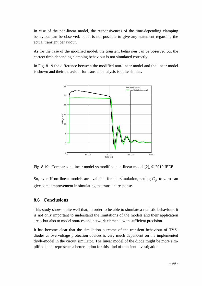
- 99 -
In case of the non-linear model, the responsiveness of the time-depending clamping
behaviour can be observed, but it is not possible to give any statement regarding the
actual transient behaviour.
As for the case of the modified model, the transient behaviour can be observed but the
correct time-depending clamping behaviour is not simulated correctly.
In Fig. 8.19 the difference between the modified non-linear model and the linear model
is shown and their behaviour for transient analysis is quite similar.
Fig. 8.19: Comparison: linear model vs modified non-linear model [2], © 2019 IEEE
So, even if no linear models are available for the simulation, setting j0C to zero can
give some improvement in simulating the transient response.
8.6 Conclusions
This study shows quite well that, in order to be able to simulate a realistic behaviour, it
is not only important to understand the limitations of the models and their application
areas but also to model sources and network elements with sufficient precision.
It has become clear that the simulation outcome of the transient behaviour of TVS-
diodes as overvoltage protection devices is very much dependent on the implemented
diode-model in the circuit simulator. The linear model of the diode might be more sim-
plified but it represents a better option for this kind of transient investigation.

- 100 -
If no linear models are available, setting the capacitance j0C to a minimum value of
0 pF can provide more satisfactory results in this specific application operating in the
reverse bias mode. Nevertheless, it is always recommended to compare simulated re-
sults with measured data.
As mentioned at the beginning of this chapter, every diode model has its advantages and
disadvantages and its different areas of application and it is always important to under-
stand given models to use them in a way to gather meaningful results.

- 101 -
9 Parameter extraction for Capacitive Coupling Clamp test
setup
This chapter deals with the measurement method of the so called capacitive coupling
clamp and the simulational approach thereof [6].
The capacitive coupling clamp test setup is a standardized immunity test method of
electronic devices against electrical fast transients (EFT) that has been established by
the International Electrotechnical Commission [39].
The capacitive coupling clamp is a measurement setup to investigate conducted elec-
tromagnetic interference without a direct galvanic connection between the cables under
test and the clamp itself.
A fast EFT pulse with a rise-time in the range of nanoseconds is applied to the coupling
clamp and the robustness of the inserted cable harness against EFT can hence be exam-
ined.
The goal of this chapter is to extract the network parameters of this test-procedure to
gather equivalent circuit models to simulate in circuit analysers like LTspice. This is
done with the use of the FEM-method described in Chapter 2.
Since the whole setup can be viewed as a multi-conductor-transmission line, the
LTspice simulation can again be carried out with the aid of the lumped-circuit approach
described in Chapter 2.
Using simulations during different design processes of electronic devices is an efficient
way to estimate the robustness of the devices against EMC-requested standards and to
prevent costly redesigns of the final product.
Analytical approaches to calculate the circuit elements can be found in [46] and [47] but
the advantage of the Finite Element Method lies in a more precise modelling of the ge-
ometry and also in the fact that the influence of the insulation material can be taken into
account without loss of accuracy.
The setup and the desired network-representation are explained in sections 9.1 and 9.2.
The parameter extraction procedure for the circuit-model is described in section 9.3.
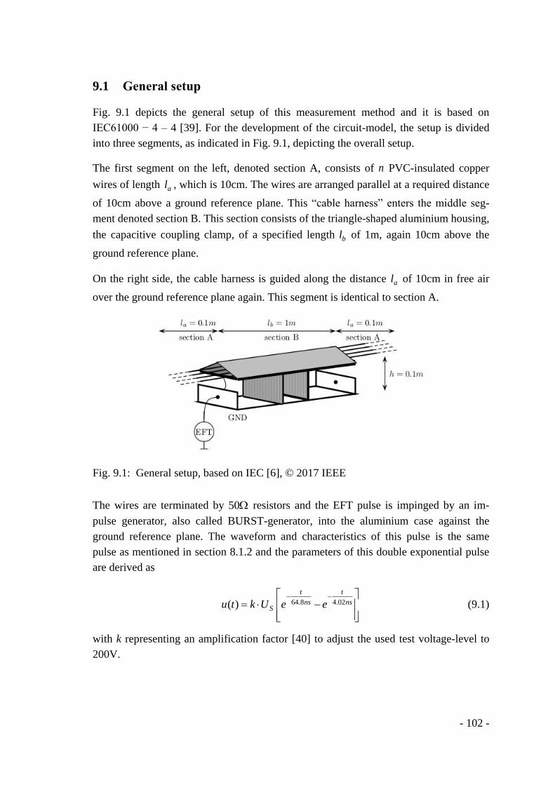
- 102 -
9.1 General setup
Fig. 9.1 depicts the general setup of this measurement method and it is based on
IEC61000 − 4 – 4 [39]. For the development of the circuit-model, the setup is divided
into three segments, as indicated in Fig. 9.1, depicting the overall setup.
The first segment on the left, denoted section A, consists of n PVC-insulated copper
wires of length al , which is 10cm. The wires are arranged parallel at a required distance
of 10cm above a ground reference plane. This “cable harness” enters the middle seg-
ment denoted section B. This section consists of the triangle-shaped aluminium housing,
the capacitive coupling clamp, of a specified length bl of 1m, again 10cm above the
ground reference plane.
On the right side, the cable harness is guided along the distance al of 10cm in free air
over the ground reference plane again. This segment is identical to section A.
Fig. 9.1: General setup, based on IEC [6], © 2017 IEEE
The wires are terminated by 50 resistors and the EFT pulse is impinged by an im-
pulse generator, also called BURST-generator, into the aluminium case against the
ground reference plane. The waveform and characteristics of this pulse is the same
pulse as mentioned in section 8.1.2 and the parameters of this double exponential pulse
are derived as
64.8 4.02( )
t t
ns nsSu t k U e e
(9.1)
with k representing an amplification factor [40] to adjust the used test voltage-level to
200V.

- 103 -
The rise time of the applied test pulse nominally is 5ns but given tolerances range be-
tween 3.5ns and 6.5ns . Therefore the fastest possible rise-time that is still within the
limit given in [39] is 3.5ns and therefore the chosen operating frequency for parameter-
extraction in section 9.3 is set to 285MHz. This is applies for developing the circuit-
model in section 9.4 as well.
9.2 Network representation of the setup
To obtain a network representation of this given setup, it is viewed as a multi-conductor
transmission line problem. For this representation, essential knowledge regarding the
mutual inductances and the coupling capacitances of the conductors and the capacitive
coupling clamp has to be gathered. In the further course, special focus is put on obtain-
ing valid and accurate circuit parameters by the use of appropriate finite element simu-
lations.
For this investigation, four parallel PVC- insulated copper wires with a conductor diam-
eter of 1.1mmd are used. The isolation thickness is 0.6mmand the relative dielectric
constant 3r for PVC is taken.
Due to the different arrangements of section A and section B of the general set-up, they
are studied separately.
Section A – Parallel wires above a grounded plane 9.2.1
For this section, the wires are placed parallel with certain distances s between each
other, 10cm above the ground reference plane as depicted in Fig. 9.2. As a consequence
the isolation material r of the wires has to be taken into consideration.
Fig. 9.2: Cross section and model dimensions of section A [6], © 2017 IEEE
The equivalent representation of this multi-transmission line model with the lumped
element approach is depicted in Fig. 9.3 where ,n nL denote the self-inductances of the

- 104 -
single wires and ,k nL the mutual inductances between the wires just as nC represents
the capacitive coupling between a single wire and the ground reference plane and ,k nC
describes the capacitive coupling between the wires. R represents the AC-resistance of
the copper wire for the selected frequency of 285MHz, modelling the impedance rise
due to the skin-effect, as it is also described in section 8.4.2.
Fig. 9.3: Circuit model of the isolated wires above grounded plane, lumped elements
[6], © 2017 IEEE
Section B – Clamp housing cables 9.2.2
Section B, consisting of the capacitive coupling clamp with the inserted wires, is depict-
ed in Fig. 9.4.
Fig. 9.4: Cross section of the model, capacitances indicated [6], © 2017 IEEE

- 105 -
The spacing between the wires and the spacing between the wires and the ground refer-
ence plane remain the same as in section A. The main difference here is that the cou-
pling clamp adds an additional conductor to this setup.
The triangular shape of the real coupling clamp is simplified by the use of two parallel
aluminium plates. In Fig. 9.4, the capacitive coupling between the coupling clamp and
the inserted wires and the clamp to ground is depicted as well.
Fig. 9.5 shows the equivalent multi-transmission line model as it can be applied for any
circuit simulator. R again stands for the AC-resistance as also mentioned in the previ-
ous section, bnnL are the self-inductances of the wires, bn,clamp
L describe the mutual in-
ductances between the n wires and the clamp plates, bk ,nL describe the mutual induct-
ances between the wires and clampL represents the inductance of the clamp-plates with
respect to the ground-reference plane.
Fig. 9.5: Circuit model of the coupling clamp housing cables above a grounded plane
[6], © 2017 IEEE
The capacitance values, also depicted in Fig. 9.5, wmC describe the mutual capacitive
coupling between the wires, wgC give the capacitive coupling between the single wires
and the clamp-plates and clampC stands for the capacitance value between the clamp-
plates and the ground-reference plane.

- 106 -
9.3 FEM- based circuit parameter extraction
To obtain the parameters for the multi-transmission line models for circuit simulators,
the electric and magnetic coupling have each to be treated with different kinds of nu-
merical FEM-computations as mentioned in Chapter 2.
The used methodologies are explained in the following sections and as mentioned in
section 9.1 the parameter extraction is done for a frequency of 285MHz.
The capacitive coupling: quasi-static electric computations 9.3.1
For the capacitive coupling, the capacitance matrices for both sections, section A [ ]AC
and section B [ ]BC have to be determined.
For section A, all capacitive coefficients of the wires against ground and all mutual ca-
pacitive coefficients as well have to be computed as they are described in section 9.2.1.
For section B, as described in section 9.2.2, the capacitive coupling coefficients be-
tween the wires and the clamp plates and the mutual coefficients of the wires itself have
to be derived. Additionally, the capacitance of the capacitive coupling in relation to the
ground reference plane has to be found as well. This leads to an additional electrode for
section B considering the clamp.
Quasi-static electric computations are carried out to derive the distributed capacitances
of every section.
In general, the setup including ground consists of n electrodes and therefore ( 1)n
FEM-computations are carried out consecutively by setting the potential of one elec-
trode to 1V while all other electrodes are set to zero potential. After each FEM-
computation, the influenced charge quantities nQ on all n electrodes can be derived
and the capacitance coefficients can be obtained as in (9.3).
The applied procedure can be summarized as:
1
1
1
1,
1
0
em
emem
n n electrodes
U V n mU
U V n m
(9.2)
1
nmn
em
QC
U (9.3)

- 107 -
and the capacitance matrix [ ]NxNC is assembled elementwise.
The number of electrodes for section A is always one less than for section B, since sec-
tion A does not include the coupling clamp.
The inductive coupling: quasi-static magnetic computations 9.3.2
For the inductive coupling, FEM-simulations using the AV,A-formulation are carried
out, as described in Chapter 2.
To gather the inductance matrices, [ ]AL for section A and [ ]BL for section B, both the
self-inductances and the mutual inductances of all conductors have to be derived, as
they are described in section 9.2.1 and 9.2.2.
Analogously to the method for the capacitive coupling, the procedure is again carried
out sequentially, but in this case a current of 1A is applied successively on each of the
conductors, whereas the other conductors remain at 0A.
The induced voltages neU due to the inductive coupling can be post-processed after
each FEM-computation and this gives knowledge of the impedance matrix [ ]NxNZ for
the multi-conductor systems. The procedure applied to both sections separately is sum-
marized as:
1,
1
0
nm
nm
nm
n n conductors
I A n mI
I A n m
(9.4)
ne
mn
nm
Uz
I (9.5)
and the impedance matrix [ ]NxNZ is assembled elementwise as in (9.5) and the induct-
ance matrix [ ]NxNL can be derived directly from these results.
Again, section B has one more conductor than section A because of the clamp.
9.4 Model for circuit simulator
After extracting the per-unit length parameters for both sections the whole setup can be
assembled. Fig. 9.6 depicts the schematic diagram of the whole setup demonstrating the
interconnection of section A and section B.
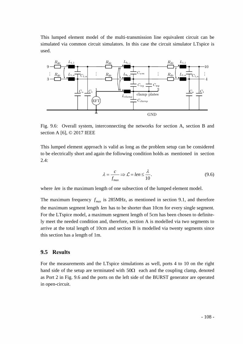
- 108 -
This lumped element model of the multi-transmission line equivalent circuit can be
simulated via common circuit simulators. In this case the circuit simulator LTspice is
used.
Fig. 9.6: Overall system, interconnecting the networks for section A, section B and
section A [6], © 2017 IEEE
This lumped element approach is valid as long as the problem setup can be considered
to be electrically short and again the following condition holds as mentioned in section
2.4:
.10max
clen
f
(9.6)
where len is the maximum length of one subsection of the lumped element model.
The maximum frequency maxf is 285MHz, as mentioned in section 9.1, and therefore
the maximum segment length len has to be shorter than 10cm for every single segment.
For the LTspice model, a maximum segment length of 5cm has been chosen to definite-
ly meet the needed condition and, therefore, section A is modelled via two segments to
arrive at the total length of 10cm and section B is modelled via twenty segments since
this section has a length of 1m.
9.5 Results
For the measurements and the LTspice simulations as well, ports 4 to 10 on the right
hand side of the setup are terminated with 50 each and the coupling clamp, denoted
as Port 2 in Fig. 9.6 and the ports on the left side of the BURST generator are operated
in open-circuit.

- 109 -
The applied maximum peak voltage for the test pulse has been set to 200 V for meas-
urements and simulations and the results are compared in Fig. 9.7.
Fig. 9.7: Comparison between simulated and measured results [6], © 2017 IEEE
The simulated output voltage is 131V and the measured output voltage is 134V which
leads to a deviation between the simulated and measured results of less than 5% indi-
cating an acceptable agreement between these two methods.
- 110 -
10 Further Work
For the FEM model so far, the apertures of the shield are inserted in a solid conducting
screen. Further investigation might contain a detailed model of the single carriers of the
braided cable shield. This might be very interesting in investigating the influence of
partially damaged cable shields of broken single strains and their influence on the trans-
fer impedance and the shielding effectiveness.
In this work, the geometry can be altered to mimic stretched or compressed cable
shields by analysing different geometries of the rhombic apertures varying the coverage
factor. Another possible task would be to extend the cable model to investigate not only
different shield geometries but also geometry deformations occurring with general cable
alterations, such as twisted or heavily bent cables. Different cable layouts will also lead
to different shield alterations and this influence might be worth investigating.
Different shielding geometries and cable types can be investigated as well and manage-
able simulation models could be developed.
For all the above mentioned cable alterations, not only the transfer impedance is a char-
acteristic parameter of interest, also the electric field penetrating the apertures has to be
investigated, especially in the case of cable harnesses and the resulting capacitive cou-
pling between cables and the effect on signal transmission.
The next step could also be to analyse cable harnesses and reliable simulation approach-
es of them, especially focusing on capacitive- and inductive coupling with respect to
electrical fast transients [48].

- 111 -
References
[1] LTspice download link, https://www.analog.com/en/design-center/design-tools-
and-calculators/ltspice-simulator.html
[2] S. Bauer et al., “Investigation of SPICE Models for Overvoltage Protection Devices
With Respect to Fast Transients,” in IEEE Letters on Electromagnetic Compatibility
Practice and Applications, vol. 1, no. 1, pp. 20-25, March 2019
[3] S. Bauer et al., “Time domain FEM computational approach for calibration of sur-
face scan method,” in IEEE International Symposium on Electromagnetic Compatibility
and 2018 IEEE Asia-Pacific Symposium on Electromagnetic Compatibility
(EMC/APEMC), Singapore, 2018, pp. 866-871
[4] S. Bauer, B. Deutschmann and G. Winkler, “Prediction of the robustness of integrat-
ed circuits against EFT/BURST,” in IEEE International Symposium on Electromagnetic
Compatibility (EMC), Dresden, 2015, pp. 45-49
[5] A. Lavarda, D. Amschl, S. Bauer and B. Deutschmann, “Characterization of the
immunity of integrated circuits (ICs) at wafer level,” in 10th International Workshop on
the Electromagnetic Compatibility of Integrated Circuits (EMC Compo), Edinburgh,
2015, pp. 196-201
[6] S. Bauer, W. Renhart and O. Bíró, “FEM-Based Computation of Circuit Parameters
for Testing Fast Transients for EMC Problems,” in IEEE Transactions on Magnetics,
vol. 53, no. 6, pp. 1-4, June 2017
[7] S. Bauer, C. Türk, W. Renhart and O. Bíró, “Finite element analysis of cable shields
to investigate the behavior of the transfer impedance with respect to fast transients,” in
IEEE 23rd Workshop on Signal and Power Integrity (SPI), Chambéry, France, 2019,
pp. 1-4
[8] C. Tuerk, D. J. Pommerenke and S. Bauer, “Improved Alternative Method For Fast
And Simple Transfer Impedance Measurements,” in IEEE Letters on Electromagnetic
Compatibility Practice and Applications, (early access)
[9] C. Tuerk, S. Bauer and D.J. Pommerenke, “Alternative Method for Transfer Imped-
ance Measurements,” (accepted) in International Symposium on Electromagnetic Com-
patibility, 2020
- 112 -
[10] S. Bauer et al., “Sensitivity Analysis of the Transfer Impedance of Shielded Cables
with Braided Shields Using a Parametrized FEM Model,” Abstract in 19th Biennial
IEEE Conference on Electromagnetic Field Computation, 2020
[11] O.Bíró, “Edge element formulations of eddy current problems,” in Computer
Methods in applied Mechanics and Engineering, Vol. 169, Issues 3-4, pp391-405, 1999
[12] O.Bíró, K. Preis, “On the use of the magnetic vector potential in the finite-element
analysis of three-dimensional eddy currents,” in IEEE Transactions on Magnetics, Vol.
25, No. 4, July 1989
[13] K. Preis, “Anwendung der Methode der finiten elemente zur numerischen Berech-
nung elektromagnetischer Felder,” Habilitationsschrift, TU-Graz, 1983
[14] K. Preis, O. Bíró, K. R. Richter, H. Resinger, K. Papp, “Nonlinear periodic eddy
currents in single and multiconductor systems,” in IEEE Transactions on Magnetics,
Vol. 32, No 3, part 1, pp. 780-783, 1996.
[15] K. Hollaus, B. Wagner, O.Bíró, “Simulation of the quasi-static electric field by an
electric current vector potential approximated by edge elements,” in COMPEL - The
international journal for computation and mathematics in electrical and electronic en-
gineering, Vol 24, No. 2, pp 581-590, 2005
[16] C.R. Paul, “Analysis of Multiconductor Transmission Lines,” in IEEE
Press, John Wiley & Sons, INC., 2008, Second Edition.
[17] C. R. Paul, ”Introduction to Electromagnetic Compatibility,” John Wiley & Sons,
INC., 2006, Second Edition
[18] S. A. Schelkunoff, “The electromagnetic theory of coaxial transmission lines and
cylindrical shields,” in The Bell System Technical Journal, Vol. 13, Issue 4, Oct. 1934
[19] A. Tsaliovich, “Cable shielding for electromagnetic compatibility,” Chap-
man&Hall, 1995
[20] R. Otin, J. Verpoorte, H. Schippers, “Finite Element Model for the Computation of
the Transfer Impedance of Cable Shields,” in IEEE Transactions on Electromagnetic
Compatibility, Vol. 53, Issue 4, Nov. 2011
[21] S. Celozzi, R. Araneo, G. Lovat, “Electromagnetic Shielding,” in IEEE Press,
Wiley- Interscience, John Wiley & Sons, INC., 2008
[22] H. A. Bethe. “Theory of diffraction by small holes,” in Phys. Rev., vol. 66, no. 7–8,
pp. 163–182, Oct. 1944

- 113 -
[23] R. E. Collin, ‘‘Field Theory of Guided Waves,” in IEEE Antennas and Propaga-
tion Society, IEEE Press, 2nd
Edition, 1990
[24] J. A. Stratton, ‘‘Electromagnetic Theory,” in IEEE Antennas and Propagation So-
ciety, IEEE Press Series on Electromagnetic Wave Theory, 2007
[25] F. M. Tesche, M. V. Ianoz, T. Karlsson,” EMC, Analysis Methods and Computa-
tional Models,” John Wiley & Sons, INC., 1997
[26] E. F. Vance, “Shielding Effectiveness of Braided-Wire Shields,” in IEEE Transac-
tions on Electromagnetic Compatibility, vol. EMC-17, no. 2, pp. 71-77, May 1975
[27] M. Tyni, “The transfer impedance of Coaxial Cables with Braided Outer Conduc-
tor,” Digest of the 10th
International Wroclaw Symposium on EMC, 1976, pp. 410-419
[28] B. Demoulin, P. Degauque, “Shielding Effectiveness of braids with High Optical
Coverage,” in Proceedings of the International Symposium on EMC, Zuerich, 1982:
491-495
[29] S. Sali, “An improved model for the transfer impedance calculations of braided
coaxial cables,” in IEEE Transactions on Electromagnetic Compatibility, vol. 33, no. 2,
pp. 139-143, May 1991
[30] T. Kley, “Optimized single-braided cable shields,” in IEEE Transactions on Elec-
tromagnetic Compatibility, vol. 35, no. 1, pp. 1-9, Feb. 1993
[31] V. I. FABRIKANT (1987), “Electrical polarizability of small apertures: analytical
approach,” in International Journal of Electronics Theoretical and Experimental, 62:4,
533-545
[32] F. De Meulenaere and J. Van Bladel, “Polarizability of some small apertures,” in
IEEE Transactions on Antennas and Propagation, vol. 25, no. 2, pp. 198-205, March
1977
[33] R. De Smedt and J. Van Bladel, “Magnetic polarizability of some small apertures,”
in IEEE Transactions on Antennas and Propagation, vol. 28, no. 5, pp. 703-707, Sep-
tember 1980
[34] H. Schippers and J. Verpoorte, “Hole inductance in braided cable shields,” in
IEEE International Symposium on Electromagnetic Compatibility (EMC), Dresden,
2015, pp. 56-61
- 114 -
[35] A. Kameari, “Calculation of transient 3D eddy current using edge-elements,” in
IEEE Transactions on Magnetics, vol. 26, no. 2, pp. 466-469, March 1990
[36] IEC 62153-4 series: “Metallic communication cable test methods, Electromagnetic
compatibility (EMC)”
[37] I. M. Sobol’, “On sensitivity estimation for nonlinear mathematical models,” in
Matem. Mod., 1990, Volume 2, Number 1, 112–118
[38] Electromagnetic compatibility (EMC) Part 4-2: Testing and measurement tech-
niques – Section 2: Electrostatic Discharge (ESD) immunity test, IEC-EN 61000-4-2,
2008
[39] Electromagnetic compatibility (EMC) Part 4-4: Testing and measurement tech-
niques – Electrical fast transient/burst immunity Test, IEC-EN 61000-4-4, 2012
[40] M. Magdowski, R. Vick “Estimation of the Mathematical Parameters of Double-
Exponential Pulses Using the Nelder-Mead Algorithm,” in IEEE Transactions on elec-
tromagnetic compatibility, Vol.52, No.4, November 2010
[41] G. Brocrad, “Simulation in LTSpice IV: Handbuch, Methoden, und Anwendun-
gen,” Swiridoff, 2013, pp. 455-459
[42] M. Reisch, “Elektronische Bauelemente, Funktion, Grundschaltungen, Modellie-
rung mit SPICE,” Springer- Verlag Berlin Heidelberg 1998, pp. 370-377
[43] J. Cao, Y. Wang, Y. Wang, G. Lu, X. Zhang, “A novel SPICE circuit model of
electrostatic discharge (ESD) generator,” in IEICE Electronics Express vol. 13 no.9,
pp. 1-8, May 2016
[44] Y. Zhou, J. Hajjar, “A circuit model of electrostatic discharge generators for ESD
and EMC SPICE simulation,” in IEEE International Conference on EDSSC, Chengdu,
China, June 2014
[45] L. Buccolini, “Simple SPICE ESD Generator Circuit based on IEC61000-4-2
Standard,” Available: http://www.youspice.com/simple-spice-esd-generator-circuit-
based-on-iec61000-4-2-standard/
[46] F. Musolino, F. Fiori, “Modeling the IEC 61000-4-4 EFT Injection Clamp,” in
IEEE Transactions on electromagnetic compatibility, Vol. 50, No. 4.

- 115 -
[47] S. Caniggia, L. Vitucci, M. Acquaroli, A. Giordano, “Measurement and SPICE
Models for Data Signal Lines Under Electrical Fast-Transient Test,” in 4th European
Symposium on Electromagnetic Compatibility - EMC EUROPE, 11-15 Sep. 2000,
Brugge (Belgium).
[48] S. Bauer, K. Hollaus, M. Leumueller, C. Tuerk, “Measurement and Modeling of
Effective Cable Parameters of Unshielded Conductors,” presented at the 19th
interna-
tional IGTE Symposium, 2020, Graz (Austria)