modified silicon surfaces via hydrosilylation reactions
TRANSCRIPT

DISSERTATION
From Silicon Wafers to Silicon Nanowires: Chemical
modification of 2D and 3D Silicon Surfaces
ausgeführt zum Zwecke der Erlangung des akademischen Grades eines
Doktors der Naturwissenschaften unter der Leitung von
Ao.Univ.Prof.Dipl.Ing.Dr. Helmuth Hoffmann
E163
Institute of Applied Synthetic Chemistry
eingereicht an der Technischen Universität Wien
Fakultät für Technische Chemie
von
M.Sc. Anders Henriksson
Matr. Nr. 0825827
Mohsgasse 25/5, 1030 Wien
Wien, am 25 Juni 2012
Die approbierte Originalversion dieser Dissertation ist in der Hauptbibliothek der Technischen Universität Wien aufgestellt und zugänglich. http://www.ub.tuwien.ac.at
The approved original version of this thesis is available at the main library of the Vienna University of Technology.
http://www.ub.tuwien.ac.at/eng

i
Acknowledgement
During my graduate studies, I have enjoyed the opportunity to meet and work with numerous
peoples.
First of all I thank Prof. Hoffmann, who gave me the opportunity to work in his group,
introduced me to a new very interesting research field, for his support, for the many good
advices and the pleasant and friendly atmosphere making my stay at Vienna University of
Technology very easy and enjoyable.
I also thank Prof. Friedbacher for AFM and SEM measurements and for his advices and the
good scientific collaboration. I thank Dr. Elisabeth Eitenberger for allways having time to
measure my samples with SEM.
Further I thank Prof. Lugstein who introduced me to the topic of silicon nanowire, Dr. Ole
Bethge for XPS measurements, DI. Johannes Greil for preparing silicon nanowire transistors,
the laborants for always providing the chemicals I needed and finally my friends and
colleagues for the support and good times.

ii
Kurzfassung
Oxidfreie Siliziumsubstrate, funktionalisiert mit organischen Monoschichten, spielen heute
eine Schlüsselrolle in verschiedenen Gebieten der Nanowissenschaften wie etwa in der
Katalyse, der Sensorik oder der Nanoelektronik. Voraussetzung für praktische Anwendungen
ist ein vielseitges und zuverlässiges Oberflächenmodifizierungsverfahren, welches die
Beschichtung von Siliziumsubstraten mit organischen Monoschichten, ausgestattet mit
bestimmten, gewünschten terminalen Funktionlitäten, mit bestmöglicher Kontrolle über
Struktur und Reaktivität der modifizierten Oberflächen ermöglicht.
In der vorliegenden Dissertation wurden Siliziumsubstrate mit unterschiedlicher Topographie
(Siliziumwafer, poröses Silizium und Silizium-Nanodrähte) hergestellt und mit organischen
Monoschichten modifiziert, welche über bestimmte funktionale Endgruppen an der
Grenzfläche Film/Umgebungsmedium verfügten. Verschiedene Modifizierungsstrategien
wurden untersucht und verglichen, zum einen die präadsorptive Synthese von Adsorbaten
mit den gewünschten terminalen Funktionalitäten und zu anderen Zwei-Stufen Prozesse, wo
auf der Oberfläche zunächst eine Primärschicht adsorbiert wird welche anschließend mittels
in-situ Oberflächenreaktionen die gewünschte Zusammensetzung erhält oder mit einer
entprechend funktionalisierten Sekundärschicht gekuppelt wird. Die Oberflächenchemie und
die resultierenden Monoschichteigenschaften wurden mit einerm Verbund verschiedener
Oberflächenmodifizierungstechniken (Reflexions-Absorptions Infrarotspektroskopie,
Ellipsometrie, Rasterelektronenmikroskopie und Kontaktwinkelmessungen) untersucht. Ein
Vergleich zwischen den chemisch identischen, aber strukturell unterschiedlichen
Siliziumsubstraten, die dem gleichen Modifizierungsprozess unterworfen wurden, ergab
siginifikante Unterschiede in molekularen Eigenschaften wie Reaktivität und
Oberflächenstruktur und makroskopischen Egenschaften wie Oberflächenbenetzbarkeit,
welche auf die unterschiedliche Oberflächentopographie der Substrate zurückgeführt
wurden. Stärken und Schwächen der verschiedenen Substrate und
Oberflächenmodifizierungsverfahren wurden untersucht und gegenübergestellt mit dem Ziel;
ein effizientes und praxistaugliches Protokoll zur Herstellung funktioneller Siliziumsubstrate
zu entwickeln.

iii
Abstract
Oxide-free silicon substrates, functionalized with organic monolayers, play a key role today in
various fields of nanoscience including catalysis, sensor fabrication and nanoelectronics.
Fundamental for practical applications is a versatile and reliable surface modification
protocol, allowing organic monolayers with certain desired terminal functionalities to be
attached to silicon substrates with a high level of control over the reactivity and structure of
the modified surfaces.
In this thesis, silicon substrates with different topographies (silicon wafers, porous silicon,
silicon nanowires) were prepared and subsequently functionalized with organic monolayers
carrying specific terminal groups located at the monolayer/ambient interface. Different
functionalization strategies were tested and compared, including pre-adsorption synthesis of
adsorbates with the desired terminal functionalities, or a two-step approach where the
surface is first primed with a precursor monolayer which is subsequently transformed by in-
situ surface reactions to the desired composition or coupled with a properly functionalized
overlayer. The surface chemistry and the resulting monolayer properties of the adsorbate
layers were investigated using a combination of different surface characterization methods
such as reflection absorption infrared spectroscopy (RAIRS), ellipsometry, scanning electron
microscopy (SEM) and contact angle measurements. A comparison between the chemically
identical, but structurally different silicon substrates subjected to identical chemical
modification procedures revealed profound differences in molecular properties (reactivity,
surface structure) as well as in macroscopic properties like the surface wettability caused by
the different surface topographies of the parent silicon substrates. Opportunities and
limitations of the different substrates and surface modification approaches were explored,
aiming at a versatile and reliable protocol for the preparation of functional silicon substrates
that can be employed for future practical applications.

iv
Publications resulting from this thesis
Henriksson, A., Friedbacher, G. & Hoffmann, H. Surface Modification of Silicon Nanowires
via Copper-Free Click Chemistry. Langmuir (2011) 27 (12), pp 7345–7348
Henriksson, A & Hoffmann, H. Structure of Alkyne Monolayers on Hydrogen-Terminated
Si(100) Surfaces Investigated by External Reflection Infrared Spectroscopy, Applied
Spectroscopy, submitted
Henriksson, A., Friedbacher G. & Hoffmann, H., Wetting Properties of Flat and Structured
Silicon Surfaces: Effect of Surface Morphology and Chemical Composition, in preparation

v
Abbreviations
AFM Atomic force microscopy
ATR Attenuated Total Reflection
CB Cassie-Baxter
CVD Chemical vapour deposition
DDDP 1,2-Decadiol-dipropiolate
DFT Density-functional theory
DMF Dimethylformamide
DMSO Dimethyl sulfoxide
DRIFT Diffusion reflection fourier transform
EDDP 1,2 Ethanediol-dipropiolate
FET Field effect transistor
FTIR Fourier transform infrared spectroscopy
HER Hydrogen evolution reaction
LB Langmuir-Blodgett
MCT Mercury cadmium telluride
NMR Nuclear magnetic resonance
NP Nanoparticle
NW Nanowire
OTS Octadecyltrichlorosilane
OWRK Owens-Wendt-Rabel-Kaeble
PL Photoluminescence
PMMA Poly(methyl methacrylate)
RAIRS Reflection absorption infrared spectroscopy
RMS Root-Mean-Square
SAM Self assembled monolayer
SEM Secondary electron microscopy
SNR Signal-to-noise ratio
TMS Tetramethylsilane
XPS X-ray photoelectron spectroscopy
TDP Tetradecanolpropiolate
TGS Triglycine sulphate
TIR Transmission infrared
VLS Vapour liquid solid
WCA Water Contact Angle

vi
Table of Content
1. Introduction .......................................................................................................................... 1 1.1. Silicon Wafers ................................................................................................................. 1
1.2. Porous Silicon ................................................................................................................. 3
1.3. Silicon Nanowires ........................................................................................................... 6
1.4. Functional Silicon surfaces based on Self Assembled Monolayers .............................. 10
1.4.1 Strategies and Applications ..................................................................................... 10
1.4.2. Organosilane monolayers on native, oxide-covered silicon ................................... 13
1.4.3. Si-C bonded monolayers on oxide free silicon ...................................................... 15
2. Characterization methods ................................................................................................. 20 2.1. Ellipsometry .................................................................................................................. 22
2.2. Contact angle Measurements ........................................................................................ 23
2.3. Infrared spectroscopy .................................................................................................... 27
2.3.1. Reflection Absorption Infrared Spectroscopy (RAIRS) ........................................ 27
2.3.2. Determining surface orientation with RAIRS ........................................................ 30
3. Experimental ....................................................................................................................... 32
3.1. Chemicals and materials ................................................................................................ 32
3.2. Substrate Preparation ..................................................................................................... 35
3.3. Chemical modification of silicon substrates ................................................................. 36
3.4. Infrared spectroscopy measurements ............................................................................ 39
3.5. Ellipsometric measurements ......................................................................................... 43
3.6. Contact Angle measurements ........................................................................................ 43
3.7. NMR measurements ...................................................................................................... 43
4. Results and discussion ........................................................................................................ 44 4.1 Preparation and properties of oxide-free planar (2D) and structured (3D) silicon
substrates. ............................................................................................................................. 44
4.1.1 Silicon (100) wafers. ............................................................................................... 45
4.1.2. Porous silicon ......................................................................................................... 47
4.1.3. Silicon Nanowires .................................................................................................. 48
4.2. Alkylation of silicon surfaces via hydrosilylation of n-alkynes .................................... 56
4.2.1. Thermal hydrosilylation on planar and nanostructured silicon substrates. ............ 56
4.2.2. Surface orientation of alkyne monolayers on Si (100) wafers ............................... 58
4.2.3 Wetting properties of alkyl modified silicon substrates .......................................... 66
4.2.4. Oxidation of bare and alkylated silicon surfaces ................................................... 69
4.3. Adsorption of activated alkynes .................................................................................... 73
4.3.1. Propiolic acid mono and diesters ........................................................................... 73
4.3.2. Reversible acid-base surface reactions of adsorbed propiolic acid. ....................... 76
4.4. Surface functionalization via click chemistry ............................................................... 80
4.4.1. Copper catalysed Huisgen cycloadditions. ............................................................. 80
4.4.2 Copper-free click reactions ..................................................................................... 82
5. Conclusion and Perspectives ............................................................................................. 92
6. References ........................................................................................................................... 95

1
1. Introduction
1.1. Silicon Wafers Semiconductors, materials which have electric conductances between metals and insulators,
are the key components of integrated circuits in any electronic equipment today with silicon
as the by far most common material employed since the beginning of the semiconductor
revolution decades ago. Silicon is a cheap and high quality semiconductor, which, as the
most abundant element on earth, is easily accessible and can be refined to purities
exceeding 9.9 (99.9999999%), thereby prevailing over more efficient semiconductor
materials like germanium with higher conductivities. Three important parameters that
characterize silicon wafers are the purity, the doping and the crystal orientation. The
manufacturing of silicon wafers is a slow process involving high purity, polycrystalline Si as
the raw product which is melted in a crucible at 1600°C. A seed crystal is immersed into the
molten silicon and rotated, resulting in the growth of a pure silicon cylinder called an ingot.
Cutting the silicon crystal into thin discs called wafers results in silicon surfaces aligned in
one of several directions known as crystal orientations. The most common orientations are
Si(100), Si(111) and Si(110). Orientation is important since many of a single crystal's
structural and electronic properties are highly anisotropic and wafer cleavage typically occurs
only in a few well-defined directions. Si(100) is the material that is currently used in the
majority of semiconductor devices largely because of a fortunate matching of the interatomic
spacing of silicon atoms with the lattice constant of silicon dioxide1
In order to influence the conductance of the silicon crystal, these are often impurified with
very small amounts of phosphorous or boron that are generally added to the molten raw
silicon during wafer fabrication, such impurification being called doping. Phosphorous atoms
are integrated into the silicon-crystal-structure but they have one extra valence electron
making the crystal slightly negative (n-silicon). Boron, on the contrary, has one less valence
electron hence inducing an electron hole into the the silicon crystal, making it slightly positive
(p-silicon). Controlled doping is the basis of modern semiconductor technology.

2
Oxide etch of crystalline silicon
Bare silicon surfaces are highly reactive and rapidly form a native oxide layer with a
thickness of several Ångström when exposed to the atmosphere. To remove this native
oxide, the silicon is exposed to a dilute HF-solution which dissolves the native oxide into
hexafluorosilicic acid. Based on the fact that Si and F form one of the strongest bonds
known, it would seem quite obvious that the silicon surface after being treated and etched
with HF is passivated with F. that is not the case, however. In fact, not even traces of F can
be detected on the surface, neither with FTIR nor with XPS. Instead it is fully covered with
hydrogen. The reason for the lack of Si-F bonds is that although it is a strong bond, it is also
highly polar, causing strain to the silicon lattice and polarizing the adjacent Si-Si bonds
which makes them sensitive to nucleophilic attacks.
In comparison, the Si-H bond is an unpolar bond, with its electrons almost evenly shared
between silicon and hydrogen. Such bonds are similar to the Si-Si bonds in the bulk and
relieve strain to the lattice. Hence, etching silicon oxide with dilute HF results in an almost
perfect H-terminated Si surface. Si(111) is terminated with Si-H monohydrides (Fig 1.1) and
forms a perfectly flat crystal surface. H-terminated Si(100) surfaces, however, form a mixture
of mono, di- and tri-hydrides which due to unfavourable steric interactions inhibit the
formation of a perfectly flat surface and a roughness of approximately 3 Å remains.
Figur 1.1. Etching of Si(100) and Si(111) in fluoride solutions (Scheme taken from Ref.1)

3
1.2. Porous Silicon Porous silicon is structured bulk silicon with nanoporous holes and of typically 1-100 nm
diameter and surface to volume ratios of several 100 m2/cm3, which change the properties of
the material dramatically. It was accidently discovered in the mid 1950s by Ingeborg and
Arthur Uhlir at Bell Laboratories in their attempt to electropolish silicon surfaces, using
aqueous solutions of HF. They noticed that under certain conditions the polishing resulted in
an unwanted uneven and sometimes coloured surface instead of the expected smooth,
polished surface. They did not explore this discovery further and it was pretty much ignored
until the late 1980s, when the porous nature, high surface area and the true surface
composition (siliconhydride) of this material was revealed and raised a moderate interest2,3,4.
A paper in 1990 by Chanman et al, describing room temperature visible photo luminescence
of porous silicon probably caused by quantum confinement, further drew the world wide
attention to this material, extensively raising the number of studies from about 200 papers
reported until 1990 to about 1500 papers 6 years later4. It has now opened new fields of
research and a current scifinder-search on porous silicon yields over 12000 hits. The
discovery of the quantum effects of porous silicon made it an interesting material for several
reasons 1) The contrast to planar silicon that is spectacularly inefficient at emitting light even
at cryogenic condition. 2) Porous silicon can be easily and cheaply prepared in a standard
chemistry labI in large quantities and time scales of e few minutes. 3) Since Si is
technologically still the most important material that dominates the microelectronic industry.
light-emitting Si devices may eventually result in a new generation of Si chips and extend the
functionality of Si technology from microelectronics into optoelectronics4. Apart from
photoluminescence, porous silicon has a number of other interesting properties for practical
applications:
It has a very large surface area to volume ratio (hundreds of m2 per cm3), making it a useful
high surface area substrate for spectroscopic studies and for sensor devices2. Porous silicon
has an increased band gap compared to planar silicon5, that and the larger surface area
make it interesting in photovoltaic applications6. Porous silicon seems to be biologically
compatible and has been used for drug delivery7,8 and as a substrate for in-vivo sensors9,10
.
Silicon Porosification
Porous silicon is formed by anisotropic etching of silicon wafers in HF solutions. As already
mentioned, bare silicon surfaces are essentially inert towards HF solution with an etching
rate in concentrated HF as slow as 0.3 Å/min. Hence, the first step in silicon etching is to
activate the surface, which is achieved by creating an electron hole in the valence band by

4
exciting an electron from the valence band to the conduction band. This is the most essential
part of silicon etching that will increase the etching rate and allow control of the etching. The
holes in the valence band can be created by applying a galvanic bias voltage, by photon
absorption or by adding an oxidant. The holes are transported to the surface of the bulk
silicon, where they weaken the bonds nearby and hence making these positions more
sensitive11.
A mechanism proposed by Gerischer et al and subsequently corrected by Kolanski11 and co-
workers is shown in Fig 1.2. The first and crucial step is always the creation of an electron
hole, which is transported to the surface. At the surface it weakens the Si-H bond and results
in its heterolytic cleavage, whereby a proton is released and one electron is transported to
the conduction band, leaving a Si radical behind. This radical reacts with a fluoride ione
under formation of a Si-F bond and transfer of one electron to the silicon valence band.
Altogether, in this first 4 step, a Si-H bond is exchanged to a Si-F bond, a proton is
abstracted and an electron is transferred to the conduction band. Alternatively, the reaction
may proceed through a SN2 mechanism with the same end result.
Once the H-passivation is broken by F-substituion, the surface is sensitive to nucleophilic
attack also without additional electron holes. This is because the Si-F bond is highly polar
causing strain to the silicon lattice and polarizing the silicon backbone as already described
in chapter 1.1. The next step is therefore a nucleophilic attack by a fluoride ion breaking a Si-
Si bond followed by a hydrogen transfer to the adjacent Si. Subsequently, two different
reaction paths are possible: Path a repeats the last step resulting in a cleavage of SiHF3
which reacts with HF in solution to form SiF62- and H2(g). In path b, a second proton is
abstracted and a second electron is donated to the conduction band forming a silicon radical.
A fluoride attacks the Si, donating an additional electron to the conduction band. A
nucleophilic attack of an additional fluoride yields SiF4 as the cleavage product, which in
solution with excess HF forms again SiF62-.
The overall etching reaction following path a is described as
Si + h+ + 6HF H2SiF6 + 2H+ + H2 + e-CB
This path is synonymous for a process called current doubling, as every electron hole
induced in the valence band yields 2 electrons in the conduction band, resulting in
photocurrent quantum yield of two.
The path b is synonymous for current quadrupling, as every induced hole in the valence
band yields 4 electrons in the conduction band.
Si + h+ + 6HF H2SiF6 + 4H+ + 3e-CB

5
Figure 1. 2. Proposed mechanisms for anisotropic etching of silicon11

6
Other mechanisms has been proposed12 , however, an electron hole at the surface, that
weakens the Si-H bond and makes it sensitive to nucleophilic attack is the essential part of
silicon etching. Surface electron holes are also a prerequisite for anisotropic etching that
does not lead to the complete dissolution of silicon but to the formation of pores. The
transport of holes to the surface is controlled by quantum confinement effects which, once
the structures reach nanoscale dimensions, passivate small structures and direct holes to the
bottom of pores rather than to pore walls.
1.3. Silicon Nanowires
Silicon nanowires (SiNW) are considered as one-dimensional semiconducting structures and
have shown novel electronic, optical, mechanical, thermal, and chemical properties. They are
expected to play a key role in applications such as solar cells13–16, sensors17–19, lithium
batteries20, and catalysts with regard to their surface-determined properties. The high surface
to volume ratios of silicon nanowires make their material characteristics to be dominated by
their surface properties rather than their bulk structure, hence they differ from bulk silicon in
many ways and form unique materials. Generally, changing the diameter of the nanowires
will change their properties. Nanowires with a diameter of less than 44 nm will oxidize
essentially slower in ambient atmosphere compared to bulk silicon due to compressive stress
normal to Si/SiO2 interface, which arises from the greater volume of SiO2 compared to Si21.
Also, the electric and thermal conductance is correlated to the nanowire diameter. Hence,
control of the nanowire diameter allows tuning of some important properties. Silicon
nanowires are also a very promising material in solar cell applications due to its very efficient
light absorption and negligible reflection. SiNW based solar cells have the potential to
increase the conversion efficiency substantially compared to bulk silicon. It is also expected
to allow cheap silicon with a high level of impurities and a large degree of defects to be used
in solar cells, hence reducing the costs substantially. Such cheap low quality silicon results in
low minority diffusion lengths, which is the average distance a charge carrier can move from
its point of generation until it recombines. Hence, the energy conversion of such low-minority
conversion lengths material is on planar substrates limited by the minority carrier diffusion,
independent of the layer thickness. An increase in the thickness will produce more light
absorption but it will not result in an increase in the device efficiency due to charge
recombination. Nanowires are superior, in comparison, because they are long in one
dimension allowing maximal absorption and thin in another dimension, thereby allowing
effective carrier collection22.

7
Silicon Nanowire Fabrication
Several different synthetic routes for the preparation of silicon nanowires, based on either
gas-phase or condensed-phase techniques, are known today. Nanowire formation can
generally be divided into bottom-up techniques and top-down approaches, where the bottom-
up approach involves growing Si-NWs from molecular precursor whereas in the top-down
approach bulk silicon is the starting material.
The bottom-up approach
The by far most frequently applied approach to form silicon nanowires is via the vapour-
liquid-solid (VLS) method by chemical vapour deposition (CVD). Briefly, in this process Si-
NWs grow on a silicon substrate in the presence of gaseous silicon precursors such as
tetrahydrosilane (SiH4) and a metal catalyst that is immobilized on the surface and is capable
of forming a low temperature eutectic phase with silicon. A thin metal film is first immobilized
onto the surface and as the surface is subsequently heated above the metal-silicon eutectic
temperature, alloy droplets are formed on the wafer. In the presence of the precursor
molecules, silicon will diffuse into this drop, which eventually will be supersaturated leading
to the precipitation of Si on the wafer-alloy interface. The alloy drop will remain above the
precipitated Si allowing further anisotropic Si NW growth23,24.
Figure 1. 3. Schematic figure illustrating the nanowire growth vapour-liquid-solid (VLS) method by chemical
vapour deposition (CVD)

8
Although nanowire growth can be catalyzed by many metals, gold is the most common
material used for several reasons: it is 1) nontoxic, 2) chemically inert, and easily available,
3) it has an eutectic point in the Au/Si binary system at a low temperature (340°C) and high
Si solubility, 4) it has a low vapour pressure at elevated temperatures, and 5) the Au–Si liquid
alloy has a high-enough surface tension to form droplets on the surface. However,
incompatibility with industrial electronic production standards is a major drawback of Au,
hence other metals should be further explored for this purpose. Until now, Ag has been the
most promising alternative metal catalyst. The VLS technique is widely used and allows
nanowires with a large range of lengths and diameters to be fabricated. By incorporating
impurities it also allows controlled doping23,24.
The top-down approach
In the top-down approach, high quality bulk silicon is the starting material and through
techniques such as photolithography25, wet and dry etching, e-beam lithography and
micromachining are nanowires formed. In contrast to bottom-up methods, which usually
require complex equipment, high temperatures, high vacuum and hazardous silicon
precursors all of which drastically increase the cost of the processes, top down approaches
are generally simpler, more cost effective and suitable for large scale production26.
One rather new top-down approach that is highly promising in this respect is metal assisted
electroless etching in HF solutions. It enables the fabrication of vertically aligned SiNWs at
low cost in large scale27. Recent improvements in the etching techniques allow the
production of well-defined nanowires of high quality, etched vertically as well as diagonally
dependant on the substrate’s orientation (Si(100) or Si (111)). The SiNWs formed by this
method will also render the properties of the silicon substrate such as the doping. SiNW
prepared with the VLS technique, on the other hand, need to be doped separately by
incorporating impurities during the NW growth.
Briefly, this process starts with the deposition of Ag nano-particles on a silicon wafer surface
via galvanic displacement in a HF/Ag solution as shown in fig 1.4. Under proper conditions
with HF and AgNO3 kept in a narrow concentration range (4.5 M and 0.1-0.5 M respectively),
the reduced Ag-particles will form a dendrimeric structure at the silicon surface. These
immobilized particles will catalyse the subsequent etching in an etchant solution containing
HF and H2O2. This allows silicon to rapidly dissolve underneath the Ag particles, forming an
uniform array of silicon pillars28.

9
Figure 1.4. Electroless etching of silicon nanowire .
There are different theories on how the silver particle participates in the reaction and
catalyses the etching. Zhu et al29 proposed that the metal catalyst facilitates the silicon
etching but will not participate in the reaction. Their hypothesis is that the etching process is
the combined result of the formation of local electrochemical cells at the silicon surface,
originated by the adsorption of metal NPs, and of the presence of hydrogen peroxide. They
proposed that H2O2 is reduced to water at the adsorbed metal NPs and that the availability of
an oxidizing agent with a redox potential located at an energy lower than the valence band
edge of Si (E0 H2O2/H2O = 1.763 VSHE, corresponding to -6.263 eV, to be compared with
the ionization energy of Si, -5.17 eV) makes it energetically favourable for electrons from
silicon to participate in this reduction process. Hence, the metal particle stays intact whereas
electron holes occur on the silicon surface. Silicon etching then proceeds as described in
section 1.2.
In contrast, Zhang et. al28 proposed that the Ag NP is partly oxidized and partially dissolved
in solution to form Ag+ ions immediately after being exposed to the HF/H2O2 solution. The
dissolved Ag+ ions then quickly react with the Si at the interfaces between the wafer and the
AgNPs, oxidizing and dissolving Si. The result is that the Ag NP will drill into the silicon
surfaces eventually forming a SiNW array.
The reactions proposed according to this mechanism are

10
Si + 4Ag+ + 6F- → 4Ag + SiF62-
2Ag + H2O2 + 2H+ → 2Ag+ + 2H2O
Yielding the overall reaction
Si + 6HF- + 2H2O2 → H2SiF6 + 4H2O
As the etching continuous, some Ag+ ions formed by this reaction may diffuse to the solution,
hence, reducing the size of the AgNPs. This would explain the cone shaped forms
sometimes seen on etched silicon nanowires, where more silicon has been etched at the top
of the wire compared to on the bottom.
1.4. Functional Silicon Surfaces based on Self Assembled Monolayers
1.4.1 Strategies and Applications
Silicon has a number of interesting properties and although it is for decades now the
standard semiconductor in electronic devices there are still enormous untapped potentials for
applications in diverse fields such as photoemission, energy transfer, sensors etc.
One field that has gained intense attention over the last 20 years is surface functionalization
with organic molecules. A molecular thin film on the surface can change the properties of the
substrate dramatically and thanks to the compatibility of silicon with conventional electronics
and the ease by which it can be structured, silicon is an ideal substrate for molecular nano
devices and allows it to be employed in such different applications such as sensing
devices19,30–32 catalysts33, electronic devices and biomimetic surfaces34,35. Electric properties
of H-terminated, oxidized and methyl terminated Si nanowires were compared by Haick and
co-workers37 and they found a 4- and 7-fold increase in conductance on H-terminated
respectively methyl terminated surfaces. Hence it is clear that the electronic properties of the
substrate can be substantially influenced by surface functionalization. Recent research
explores this further and has aimed at controlled tuning of the electronic properties such as
the conductivity. Controlling these properties is fundamental in semiconductor devices like
field-effect- transistors (FET) and is now largely achieved by gating and impurity doping.
However, as semiconductor devices shrink to nanoscale dimensions such as single
nanowires, routine methods may fail to achieve homogenous doping. Hence, great effort has
been spent lately, aiming to develop alternative doping strategies38,39,40,41, 42 . One approach
is to immobilize a thin organic monolayer film carrying electron deficient or electron rich
groups onto the surface. Charge transfer can then occur between the silicon surface and the

11
grafted molecules, influencing the electronic properties38. The large surface-to-volume ratio
of porous silicon provides high-efficiency surface modification and functionalized silicon
nanowires can among others be employed to control the conductance in silicon nanowire
transistors.
Figur 1. 5. Some applications of self-assembled monolayers in nanotechnology (Scheme taken from Ref36)
Sensors devices is another hot topic which has been employed for various applications.
Lately a nanowire FET-sensor has been developed that allows label free detection of DNA43
and volatile organic compounds44. One other topic extensively studied is energy conversion
and among others photovoltaic applications45 and the hydrogen evolution reaction (HER)
where water is spitted forming hydrogen gas46. Most semiconductor surfaces, including
silicon, are poor catalysts for this reaction. Semiconductor water-splitting devices, then,
generally require a chemically distinct catalyst in order to store energy as molecular
hydrogen. Platinum has often been used in the past for this purpose, since it catalyzes the
HER very efficiently. Masuda et al33 demonstrated that if Pt complexes are placed at
controlled positions at silicon surfaces they act as confined molecular electrocatalysts for
hydrogen evolution at a semiconductor electrode surface without being converted into metal
clusters or particles.
To enable such applications surface films with well-defined packing and density of specific
molecules as well as full control of the formation of these films are required. A molecular

12
nano device demands a high level of control over the reactivity and structure of the modified
surfaces as well as a very high quality of the molecular film attached to the surface. Reliable
protocols to prepare functional surfaces that for example, contain components to couple a
further functionality or components that can interact with the environment are required.
Molecular films fulfilling these demands can be prepared using the Langmuir-Blodgett
methodology, which is a well established and sophisticated technique to form laterally
structured monolayers47 These films are formed when amphiphilic, surfactant-like molecules
are placed at the air-water interface. The hydrophilic head groups are attracted to the water
and the hydrophobic tail groups organize and pack themselves to form an ordered
monolayer.
Another common modification procedure is to use self-assembled monolayers which can be
described as a chemisorbed layer of organic molecules that under certain conditions
spontaneously organize to form ordered, well defined adsorbate layers. The substrate is
typically immersed into a solution of amphiphilic precursor molecules, containing a head
group with a high affinity to the substrate and a hydrophobic tail group that through van der
Waals interactions adopt a uniform, densely packed surface orientation with uniaxial
symmetry around the surface normal. Due to their covalent bonding to the substrate, these
layers are generally more stable than Langmuir-Blodgett films. Self-assembled monolayers
were discovered through the adsorption of alkylsulfides on gold substrates almost 30 years
ago and have been a hot topic over the last 10-15 years with a steeply increasing number of
publications and applications in the a wide variety of fields36. SAM modification protocols are,
in addition to silicon, also available for other substrates, such as gold36, silver48, platinum49,
glass50, and various metal- and metalloid oxides51. The monolayers can be attached to the
substrate by covalent, ionic or coordinative bonds and a large variety of surface properties
have been successfully demonstrated.
Generally there are two strategies to attach a desired functional group onto a substrate
surface. Either you synthesize the whole molecule prior to adsorption or you use of a two-
step approach by which the surface is first primed with a precursor monolayer which is
subsequently transformed by in-situ surface reactions to the desired composition or coupled
with an overlayer carrying the desired surface functionality. They both have their advantages
and disadvantages and which strategy to choose depends completely on the system.52
The main advantage in using the pre-synthesis approach is that the synthesis, purification
and characterizations of the desired SAM-forming molecules can be completed in a
controlled manner using standard methods. A 2 step approach is more complex and
chemical reactions that work perfectly in solution might be completely inactive on the surface.

13
Because of very limited possibilities for purification reaction side products should be avoided
and a 100% reaction yield is required to prevent unreacted sites to be present on the
surface52.
However the pre-synthesis approach has several disadvantages. It demands more synthetic
efforts and because of incompatibilities between the desired SAM forming molecules and the
adsorption protocol the approach might be impossible. In the pre-adsorption approach, a
reactive anchor layer is attached to the surface in a step-wise fashion and often commercially
available compounds can be used, thereby enabling a large variety of interfaces to be
prepared with limited efforts. However, most problems with pre-adsorbed molecules occur
because of incompatibilities between the desired molecule and the attachment procedure. It
can be that the reaction conditions which might be very harsh destroy the functionality or that
the functionality interferes with the monolayer formation. An example of a case where the
functionality is very sensible to the reaction conditions is the adsorption of proteins in
biosensing application. The proteins are required to remain folded with the biological
functions intact which restricts the reaction conditions (temperature, solvent etc.) to a very
narrow range which might seriously hamper the adsorption. In addition to the
incompatibilities with the modification protocol, the desired functional SAM-forming molecules
might be too bulky to allow a perfect coverage of the surface, hence preventing the formation
of a monolayer with the desired quality52.
1.4.2. Organosilane monolayers on native, oxide-covered silicon
Since the pioneering work of Sagiv et. al.53, studying the adsorption of long-chain trichloro-
and trimethoxy silanes on oxidic surfaces, this class of compounds has been the by far most
studied system to functionalize silicon surfaces. The monolayer forms via a condensation
reaction between the hydrolyzed trichloro- or trimethoxysilane and the hydroxyl groups of the
oxide surface (Fig 1.6). As silicon in open atmosphere is always covered with a thin, native
oxide layer, this protocol is very suitable for the functionalization of silicon surfaces. During
the past 30 years of intense research on these monolayers, the reaction mechanism has
been frequently debated and conflicting results have repeatedly been reported. Although the
monolayer preparation protocol is simple for reproducible, high quality monolayers a number
parameters such as precursor concentration, solvent, temperature, deposition time, water
content and age of the adsorbate solution have to be carefully chosen, since small deviations
may result in very different qualities of the monolayers54–56. Water seems to play a major role
in the condensation reaction affecting the order, the kinetics and the growth mechanism.
Exposing oxidized silicon surfaces to organo silanes at moderate temperatures in water

14
containing organic solvents, will result in an islands monolayer growth where the silanes are
believed to react with the water and aggregate in solution before it binds to the silicon
substrate57. Monolayers formed at high temperatures tend to give a less densely packed film
and favours homogeneous growth over islands growth. A critical temperature Tc has been
observed where the transition between island growth and homogeneous growth occurs.
Temperatures below Tc favour island growth and temperatures above Tc favour
homogeneous growth. Tc is correlated to the chain length. Increasing the chain length
increases Tc, hence short chain organo silanes tend to grow homogeneously and result in a
less densely packed and more disordered film compared to long chain compounds58.
Monolayer growth in water-free environments seems to proceed slowly and results in less
densely packed monolayer, however the growth of islands has been observed even under
these conditions.
Organo silanes are oriented almost parallel to the surface normal, tilted by only 8-10°, which
makes them very similar to Langmuir-Blodgett films. The monolayers are also remarkable
stable and survive in boiling water and organic solvents and are also quite resistant to acid
solutions.
Figure 1. 6. Monolayer formation of trichlorosilanes adsorbed on silicon substrate covered with a native oxide.
However, there are also several disadvantages with this modification protocol and its
implementation for the fabrication of molecular devices. A dielectric oxide layer separating
the organic functionality and the silicon substrate will decrease the electrostatic response in
sensor applications and cause fluctuations in electronic devices. Sensor responses are also
highly affected by the presence of interface traps often appearing at oxide surfaces
decreasing its efficiency even more. Other major obstacles are the sensitivity of these
organosilane monolayers to basic solution, resulting in fast degradation of the monolayer.
This prevents pH sensing and sensing in alkali solutions54. Silicon oxide is also known to
destabilize photoluminescence in porous silicon and thereby preventing such monolayers to
15
passivate the surface for such applications59. Moreover, the unstable PL properties of light-
emitting PSi are believed to be mainly due to the generation of nonradiative recombination
centers at the initially H-terminated Si surface upon oxidation during air exposure or photo-
oxidation59. Despite these drawbacks, condensation of trichloro silanes onto oxide surfaces
is one of the most reliable ways to form well packed monolayers and by adding a terminal
functionality, functionalized silicon surfaces for various applications have been achieved54
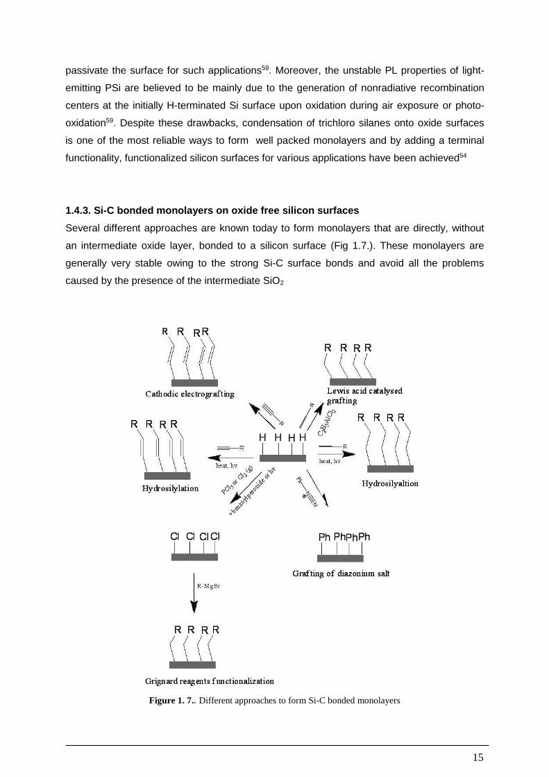
1.4.3. Si-C bonded monolayers on oxide free silicon surfaces
Several different approaches are known today to form monolayers that are directly, without
an intermediate oxide layer, bonded to a silicon surface (Fig 1.7.). These monolayers are
generally very stable owing to the strong Si-C surface bonds and avoid all the problems
caused by the presence of the intermediate SiO2
Figure 1. 7.. Different approaches to form Si-C bonded monolayers

16
Hydrosilylation
Among the methods to attach organic molecules to oxide free silicon surfaces under
formation of a covalent Si-C bond, the hydrosilylation reaction of alkynes or alkenes on H-
terminated silicon surfaces is probably the most versatile and best studied route (Fig. 1.8).
Typically, to initiate the reaction between a hydrogen terminated surface and a terminal
alkyne or alkene, heat or UV light are employed but also visible light and sonication60 has
been reported.
Figure 1.8. Hydrosilylation between a hydrogen terminated silicon surface and an alkyne or an alkene
The mechanism of this reaction is still controversial and seems to depend on the type of
activation employed. The thermally activated hydrosilylation mechanism is probably the least
debated and is generally accepted as a radical chain propagation (Fig. 1.9a). The initial step
is a thermal cleavage of a Si-H bond, forming a silyl radical at the hydrogen-terminated
silicon surface, known as a dangling bond. The silyl radical then attacks the alkene or alkyne
resulting in a new covalent Si-C bond and a migration of the radical to the β-carbon atom.
Subsequently one hydrogen atom is abstracted from a neighbouring Si-H bond at the
hydrogen terminated silicon surface resulting in a Si-C bonded alkyl or alkenyl group and a
new dangling bond at the silicon surface. This dangling bond can then react with another
hydrocarbon chain and in this way the monolayer formation propagates across the surface61.
Using deuterium terminated silicon surfaces, this mechanism has been experimentally
confirmed on different silicon substrates such as flat silicon, porous silicon62, SiNWs and
SiNPs63 and theoretical studied using DFT calculations64. The latter DFT study indicated that
due to a lower H-abstraction energy barrier and a larger overall reaction enthalpy the
reaction with terminal alkynes should be faster than with corresponding alkenes and should
also lead to a more stable organic overlayer. This was later experimentally confirmed by two
independent studies by Ciampi et.al 65 and Scheres et.al.66 Typical reaction conditions for

17
thermally induced hydrosilylation reactions are neat alkyne/alkene at temperatures above
160 °C, a reaction time of at least 3h and and rigorous exclusion of oxygen. Hydrosilylation
on porous silicon seems to demand less harsh reaction condition compared to flat silicon and
has been successfully carried out in refluxing toluene at 110 °C62.
For photo-initiated hydrosilylation reactions, four mechanisms have been proposed (Fig. 1.9):
(i) Si H bond homolysis followed by a radical reaction as described above (ii) photoemission:
Photo induced electron emission followed by a nucleophilic attack on the positively charged
silicon and hydrogen migration (iii) plasmon-mediated and (iv) exciton-mediated initiation: A
valence band electron is excited to the conduction band and is stabilized through coulomb
interaction with the formed electron hole in the valence band 61
Figure 1. 9. Hydrosilylation reaction mechanisms proposed by Buriak and co-workers (Scheme taken from Ref
61)
The mechanisms proposed for UV-initiated hydrosilylation are Si-bond homolysis and
photoemission. Visible-light induced hydrosilylation is in addition to photoemission proposed
to involve the formation of plasmons or quantum-confined exciton. The radical chain reaction
is not likely to happen, since visible light has insufficient energy to break the Si-H bond. The
mechanism of white-light initiated hydrosilylation reactions seems to follow a different route
compared to UV or thermal initiation and proposals involving both plasmons and excitons
have been presented. A result strongly in favour of the exciton mechanism is that efficient
white-light adsorption has only been observed on photoluminescent, porous silicon. As

18
photoluminescence originates in the recombination of excitons, this is a strong indication
supporting the exciton hypothesis.
Si(111) surfaces are in general easier to functionalize than Si(100), independent ofn the
functionalization strategy. The reason for this is the higher surface roughness of Si(100)
disturbing the monolayer formation and its more rapid oxidation making it more sensitive to
unwanted oxygen in the reaction vessel.
Grafting of diazonium salts
In addition to the hydrosilylation reaction one promising way to functionalize oxide-free silicon
surfaces with an organic layer is through electrochemical deposition of diazonium salts
carrying the desired functionality (Fig 1.7). This method is very interesting because it can be
used to modify a large variety of surfaces in addition to H-terminated silicon such as oxidized
silicon67, carbon, gold, platinum and more52. Thin films with a broad variety of functionalities
have been prepared and the grafting can be carried out in aqueous as well as non-aqueous
environments. The diazonium salts are relatively easy to prepare and the functionalized
aromatic groups could be further modified by classical chemical reactions. However, packing
densities and monolayer qualities are, in general, not as good as with other adsorption
protocols.
Reactions with halogen terminated surface
Silicon surfaces can also be functionalized by reaction of a Grignard reagent (R-MgX)
carrying the desired functionality with a halogenated silicon surface, prepared in the gas
phase under UV-irradiation68 or in solution phase by reaction with PCl569 An almost 100%
surface coverage was obtained when methyl groups were introduced using this approach,
resulting in an excellent protection against oxdiation37,69. However, this Grignard reaction is
essentially limited to alkyl substituents with few options for further functionalization, hence
limiting its practical applicability. Other drawbacks associated with this strategy are the
hazards of Grignard reagents and the two step modification procedure instead of a direct one
step modification in the hydrosilylation approach.
Pros/Cons Si-C bonded monolayers
The above described modification protocols for organic monolayers directly bonded onto
bare silicon surfaces through Si-C bonds avoid many problems associated with organosilane

19
monolayers on oxide-covered silicon. There is no insulating layer separating the desired
organic functionality from the surface, the monolayers are very stable also in alkaline
solutions, there are no interface traps destroying photoluminescent properties. A variety of
approaches including thermal, ultraviolet and visible light hydrosilylation, electrografting of
diazonium salts and Grignard reactions leaves many options to adapt the adsorption
conditions to the specific, required surface functionalities. Many reports in the literature have
proven successful covalent grafting of a large variety of functionalities either through pre-
syntheses adsorption or through multi step attachment procedures. Reactive H-terminated
silicon surfaces can relatively easy be prepared through etching of the native silicon oxide
layer in HF. Due to steric reasons, monolayers of long chain hydrocarbon yield a maximum
coverage of about 50% of the reactive Si-H sites. In spite of that, its oxidation protection and
electrical insulating properties are excellent70. However, several fundamental questions are
still unanswered, for example the conflicting results about the different adsorption
mechanisms, the optimal conditions of the functionalization or the influence of the substrate
morphology on monolayer formation and monolayer properties.

20
2. Characterization methods
As described in the last chapter, there are large amount of options to functionalize silicon
surfaces with self assembled monolayers. However, once you have decided which approach
that suits the system best, another great challenge remains, its characterization.
Method What is
measured?
Information
yielded
Complexity Advantages Disadvantages
Contact angle
Surface energy
Expected hydro (or solvo) phobicity; Small hysteresis (indicates homogeneity)
Low Simple, fast, sensitive. non-destructive
Contamination-sensitive
Elipsometry Thickness Layer thickness Refractive index
Low Simple, fast, non-destructive, non contact.
Contamination sensitive,
FTIR Molecular vibrations
Chemical
composition
profile.
Packing density
Molecular
orientation;
Medium Fast, non-destructive, Chemical and structural information
Contamination sensitive, Insensitive to some, vibrations/ orientations
XPS Core levels Elemental composition, chemical state, impurities
High Detects elements; Quantitative down to % of monolayer
Destructive, Limited extraction of vertical profile, slow, expensive
AFM Microscopic height & Position
Surface topography, surface structure (periodic and non-periodic
High Sub-microscopic lateral and depth information
Limited integration capability, tip dependence
Table 2.1. Overview of monolayer characterization methods45
The above mention techniques (table 2.1) were employed in this thesis to characterize self
assembled monolayers. These techniques provide detailed information for characterizing
monolayers and monitoring surface reaction. The most important informations for this thesis
were extracted from contact angle measurements, ellipsometry and FTIR, hence these 3
methods are described in more detail in this chapter. However, in addition to the methods in

21
table 2.1 there are a plethora of other techniques that in the literature are frequently used to
characterize monolayer (table 2.2.).
Experimental technique Information that can be obtained
Electronic techniques
Auger electron spectroscopy (AES) Surface elemental composition, growth mode, Coverage
X-ray photoemission spectroscopy (XPS) Elemental composition, chemical state, impurities
Ultraviolet photoemission spectroscopy (UPS) Valence band, density of occupied states, bonding nature, band dispersion
X-ray absorption near edge spectroscopy (XANES)
Conduction band, density of empty electronic
states, molecular orientation, bonding nature
High-resolution electron energy loss
spectroscopy (HREELS)
Adsorbate vibrations, phonons, adsorption sites
Structural techniques
Extended x-ray absorption fine structure (EXAFS)
Structural parameters. Atomic distances, molecular Orientation, thermal vibrational amplitudes. Coordination number
Programmed thermal desorption (TPD) Adsorption energies and site
Low-energy electron diffraction (LEED) Surface symmetry, atomic distances, molecular orientation, thermal vibrational amplitudes (needs periodicity)
X-ray diffraction (XRD) Grazing incidence x-ray diffraction (GIXD)
Crystal structure, atomic distances, molecular orientation, thermal vibrational amplitudes (needs periodicity), degree of order or crystallinity
Ion scattering spectroscopy (ISS) Time of flight direct recoil spectroscopy (TOF-DRS)
Surface structure and composition, H detection
Infrared spectroscopy (IR) Infrared reflection–absorption spectroscopy (IRAS)
Specific chemical groups, adsorption site, surface orientation
Surface plasmon enhanced Raman spectroscopy
Adsorbate vibration, surface phonons, molecular tilt
Atom scattering/diffraction Surface structure
Sum frequency generation (SFG) Adsorbate vibrations, surface coverage, conformation of alkyl chains, adsorbate–substrate bond
X-ray standing waves (XSW) Bond distance, adsorption site
X-ray reflectivity (XRR) (and also Neutron reflectivity, NR)
Surface normal relaxations, surface roughness, interface and thin layer thickness
Microscopic techniques
Scanning tunnelling microscopy (STM) Surface topography, surface structure (periodic and non-periodic)
Atomic force microscopy (AFM) Surface topography, surface structure (periodic and non-periodic)
Scanning tunnelling spectroscopy (STS) Local electronic states, single molecule conductance
Table 2.2. Surface science techniques for characterization of SAMs.71

22
2.1. Ellipsometry
Ellipsometry is a fast and simple method that is generally used to determine the optical
properties and thickness of different materials by detecting changes in light polarization
caused by reflection or transmission from the material. Important advantages with
ellipsometry is the easy, fast and non-destructive measurement procedure providing the
optical properties of the material and reliable film thicknesses down to 0.1 nanometer at
sample areas as small as 1 mm2.
Light travelling through space can be described as an electromagnetic wave with an electric
field orthogonal to the direction of propagation. Light from a source such as He/Ne is
unpolarized which mean that the orientation and phase of the electric field is completely
random oriented. The light will be linearly polarized when the two oscillating orthogonal light
waves are in phase (fig 2.1). If the orthogonal waves are 90° out-of-phase and equal in
amplitude, the resultant light is circularly polarized, elliptical polarization occur if orthogonal
waves of arbitrary amplitude and phase are combined
By elipsometric measurements, Monochromatic light travels through a filter that polarize the
light linearly, as the linearly polarized light is reflected from a surface, the phase and
amplitude of the electric waves changes, resulting in an elliptically polarized beam The now
elliptically polarized light is passed through a second polarizer, called the analyzer, that again
polarize the light linearly and the light intensity is subsequently detected by the detector as a
function of the angle of the analyzer. The phase and amplitude change (tan ψ) and the phase
difference (Λ) are analyzed to extract the optical properties of the material yielding
information such as the refractive index, the film thickness and surface roughness.
Figure 2.1 Schematic illustration of the construction of an ellipsometry

23
2.2. Contact angle Measurements
Information about surface energy, surface roughness and surface heterogeneity can be
obtained by measuring the angle at which a liquid vapour interface meets a solid surface 72,73
Contact angle measurements is then a powerful tool to characterize self assembled
monolayer as the measurement is fast, non-destructive and the obtained surface free energy
varies widely with the types of functional groups on the surface. For hydrophobic surfaces,
the free energy decreases in the order -CH2>-CH3>-CF2>-CF2H>-CF340, making the contact
angle sensitive to surface reactions and structural changes of the monolayer. For a self-
assembled alkyl monolayer adsorbed on the surface, well-ordered monolayer will expose the
CH3-groups with a different surface energy than CH2-gróups exposed in a disordered
monolayer. Perfectly ordered alkyl monolayers adsorbed on flat surfaces generally generate
a water contact angle of 109°-111° whereas defects immediately decreases this angle,
hence providing information about the monolayer quality
There are various ways to carry out contact angle measurements, one common method is
the sessile drop approach, there a liquid drop will be advanced very slowly over the surface
via a syringe mounted above, and the contact angle θ is subsequently measured with a
goniometer. If the substrate has an attractive force on the liquid the drop will wet the surface
at a relatively large contact area. If contrariwise the force between the surface and the liquid
is repulsive, the liquid will have a small contact area, hence a large contact angle is
recorded. Generally you say that liquids with contact angles below 90° are wettable or
lyophilic whereas surfaces with larger contact angles are dewetting or lyophobic.
Figure 2.2 Contact angle of a liquid droplet wetted to an ideal solid surface.
The contact angle of a liquid drop on a solid surface is defined by the molecular interactions
across the liquid/vapour, solid/vapour, and solid/liquid interfaces. The relation between them
is known as the Young's equation:

24
2.1.
where θ is the measured contact angle, γlv is the free surface energy of the liquid in contact
with vapour, γsv is the free surface energy of the solid in contact with vapour and γsl is the
free surface energy of a solid covered with liquid. Young's Equation contains only two
measurable quantities, the contact angle θ and the liquid–vapour surface tension, γlv. To
determine γsv and γsl from contact angle measurements, a couple of models are available,
such as the Neumann Model75 or Owens-Wendt-Rabel-Kaeble model (OWRK)76.
Micro and nano structures on the surface have a strong influence on the wettingproperties
and the Young equation isn’t valued on such surfaces. There are two major types of
mechanisms that explain the effect of roughness on the apparent contact angle of liquid
drops, known as the Wenzel Model and the Cassie-Baxter model77. These can be described
as
cos θc = r(γSV − γSL)/LV = r cos θ Wenzel Model 2.2.
and
cos θc = f1 cos θ1 + f2 cos θ2 Cassie-Baxter (CB) 2.3.
were θc is the contact angle, θ is the contact angle on flat surfaces, the r is the roughness
and f1 and f2 are the projected area fraction of the liquid and the air
Figure 2.3. Young model, Wenzel model and Cassie-Baxter model
Wenzel characterized rough surfaces by a roughness ratio factor ”r” defined as the ratio of
the true area of the solid surface to its projection i.e., r = Arough/Aflat Adding the roughness

25
ratio factor ”r” in Young’s equation (γSV becomes rγSV and γSL becomes rγSL) gives the
Wenzel equation, The Wenzel Model assumes that the liquid wets all of the rough surfaces,
and the equation immediately suggests that the increased total surface area geometrically
enhances hydrophobicity, θ>90 and hydrophilicity for θ<90 78 as illustrated in fig 2.4.
Effect of Substrate Roughness on Contact Angle (WENZEL model)
0
20
40
60
80
100
120
140
160
180
1 1,5 2 2,5 3 3,5 4
roughness r
co
nta
ct
an
gle
Figure 2.4. The contact angle for a defined θ as a function of surface roughness calculated with the Wenzel
equation.
The next model, the Cassie-Baxter Model, describes the presence of a heterogeneous solid
surface that has domains with different surface free energies. This model considers the
interface composed of two types of domains: fraction f1 with contact angle of θ1, and fraction
f2 with contact angle of θ2 where f1+ f2=1. If one of the 2 components is air with a contact
angle of 180° the Cassie-Baxter equation can be simplified as
cos θc = f(cosθ+1) – 1 2.4
In contrast to the Wenzel relation, the Cassie relation allows of θc > 90°, even with θ < 90° if
f are small, fig 2.5.

26
Effect of substrate porosity (1-Φs) on contact angle (CASSIE Model)
0
20
40
60
80
100
120
140
160
180
0 0,1 0,2 0,3 0,4 0,5 0,6 0,7 0,8 0,9 1
Substrate Porosity p
Co
nta
ct
an
gle
Figure 2.5. The contact angle for a defined θ as a function of surface roughness calculated with the Cassie-
Baxter equation,
27
2.3. Infrared spectroscopy
A molecule can vibrate in various different ways, for a non-linear molecule with N atoms
there are 3N-6 different vibrations, and depending of the art of vibration, the masses of the
atoms involved and the strength of the bond, those vibrations oscillate at different
frequencies. Smaller masses oscillate at a higher frequency because they are lighter and
easier to move than larger masses. Deformation vibrations oscillate at lower frequencies
compared to corresponding stretching because it is easier to bend a bond than to stretch or
compress it. A molecular vibration is excited when the molecule absorbs a quantum of
energy, corresponding to the vibration's frequency. Such vibration transitions typically require
an amount of energy in the range of infrared radiation, allowing these vibrations, which are
characteristic for functional groups, to be probed with infrared spectroscopy.
One of the greatest strengths of Infrared spectroscopy compared to other characterization
methods is that it allows solid, liquid as well as gas phases to be characterized. For example,
if the sample is a powder it can be finely grounded together with KBr, and subsequently
measured in diffusion reflection or pressed into a thin disk to be measured in transmission.
Liquid samples are often sandwiched between two windows (for example KBR) and
measured in transmission. The spectrum is divided with a reference spectrum, containing
only KBr, to remove unwanted background contributions in the sample spectrum.
Infrared spectroscopy is also an important tool in analysing thin films on surfaces due to the
low cost, minimum sample preparation and the direct information about the surface
composition that can be provided. Thin films on flat surfaces can be characterized with
reflection methods such as Attenuated total reflection (ATR) and Reflection Absorption IR
(RAIRS) or in transmission IR (TIR). Nanostructured surfaces such as porous silicon and
silicon nanowire scatter the incident bream, hence characterized in diffuse reflection IR
(DRIFT) or transmission IR (TIR).
2.3.1. Reflection Absorption Infrared Spectroscopy (RAIRS)
In Reflection Absorption Infrared Spectroscopy, the infrared beam hits the film in a defined
incidence angle, passes through, is reflected at the substrate and passes the film again
before it finally hits the detector. The absorption is commonly expressed as -log (Rs/R0),
where Rs is the sample (substrate plus adsorbate) reflectivity and R0 is the reflectivity of a
clean reference substrate. It is today a well-established technique for spectroscopic
characterization of flat surfaces and provides information about the chemical composition as
well as structural information such as the surface orientation of adsorbates. The interaction
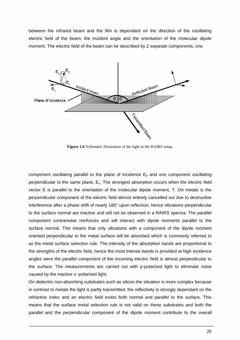
28
between the infrared beam and the film is dependant on the direction of the oscillating
electric field of the beam, the incident angle and the orientation of the molecular dipole
moment. The electric field of the beam can be described by 2 separate components, one
Figure 2.6 Schematic illustration of the light in the RAIRS setup.
component oscillating parallel to the plane of incidence Ep and one component oscillating
perpendicular to the same plane, Es. The strongest absorption occurs when the electric field
vector E is parallel to the orientation of the molecular dipole moment, T. On metals is the
perpendicular component of the electric field almost entirely cancelled out due to destructive
interference after a phase shift of nearly 180° upon reflection, hence vibrations perpendicular
to the surface normal are inactive and will not be observed in a RAIRS spectra. The parallel
component contrariwise reinforces and will interact with dipole moments parallel to the
surface normal. This means that only vibrations with a component of the dipole moment
oriented perpendicular to the metal surface will be absorbed which is commonly referred to
as the metal surface selection rule. The intensity of the absorption bands are proportional to
the strengths of the electric field, hence the most intense bands is provided at high incidence
angles were the parallel component of the incoming electric field is almost perpendicular to
the surface. The measurements are carried out with p-polarized light to eliminate noise
caused by the inactive s.-polarized light.
On dielectric non-absorbing substrates such as silicon the situation is more complex because
in contrast to metals the light is partly transmitted, the reflectivity is strongly dependant on the
refractive index and an electric field exists both normal and parallel to the surface. This
means that the surface metal selection rule is not valid on these substrates and both the
parallel and the perpendicular component of the dipole moment contribute to the overall

29
absorption. The existence of an electric field parallel to the surface allows s-polarized light to
Figure 2.7. a) Calculated reflectivity differences between the clean substrate (R0) and an isotropic adsorbate-
covered substrate (Rs) on a silicon surface. The solid line correspond to p-polarized light and the dashed to s-
polarized light. b) Calculated reflectivity differences between the clean substrate (R0) and an isotropic adsorbate-
covered substrate (Rs) on a gold surface In (c) calculated absorbances - log Rs/R0 of the hypothetical adsorbate
vibration at 3000 cm2 on a silicon surface as a function of the light incidence angle p-polarized radiation The
light are denoted with Ax and Az represent the parallel and perpendicular x z components, respectively, of the
total absorbance Ap, and u B is the Brewster angle. The same optical constants as in (a) were used for substrates
and adsorbate (Data taken from Ref 79)
be employed for spectroscopic surface characterization to detect surface vibration
perpendicular to the surface normal and p-polarized light, having both a parallel and a
perpendicular vector to detect both. In picture 2.7 published by Brunner et.al79, calculated
reflectivity differences between the clean substrate (R0) and the adsorbate-covered substrate
(Rs) illustrates that both R0 and Rs on dielectric substrates depend strongly on the incidence

30
angle and polarization of the infrared radiation. A complex IR spectra is provided were the
reflectivity change R0 - Rs upon absorption is not always positive, as one would expect as a
consequence of light being absorbed by the sample, but can also due to an increase in
reflectivity upon absorption be negative, resulting in inverted bands in the reflection
spectrum. Absorption of S-polarized light will exclusively give such inverted bands with a
maximum with angle of incidence below 60° whereas the reflectivity profile of p-polarized
light is more complex and depended on the incidence angle and the orientation of the dipole
moment since it interact both with perpendicular and parallel surface vibrations. The
contribution of parallel and perpendicular vibrations to the overall band intensity is described
in equation 2.4 and illustrated in fig 2.7 c from which can be concluded that their contribution
to the intensity is in opposite direction55,79,80.
αkαkR
RI(α sincos
0
S2
2
2
1)
2.4.
2.3.2. Determining surface orientation with Reflection absorption infrared spectroscopy
The orientation of an ordered anisotropic uniaxial organic carbon chain in respect to the
silicon substrate can be described by 3 angles as illustrated in figure 2.8. The angle α is the
angle between the molecular backbone and the surface normal, the twist angle β describes
the rotation of the hydrocarbon chain plane with respect to the molecular axis; and the angle
of precession (ψ) describes the tilt direction36. Most monolayer on most substrates have an
isotropic oriented ψ described with the “magic angle”, 54.7° and an 45° twist angle, which
means that in most cases the tilt angle α is the only unknown parameter.
Figure 2.8. Long chain alkyne adsorbed on a Silicon substrate

31
A carbon chain adsorbed on a surface, exhibit 4 main stretchings in the 3000 region, 2 CH2
absorptions at 2920 cm-1 (as(CH2)) and 2850 cm-1(s(CH2)) and 2 CH3 stretchings at 2963
cm-1(asCH3)), 2872 cm-1 (s(CH3)). The direction of their dipolmoment is correlated to the tilt
angle α, hence changing the tilt angle results in different absorbing band intensities and
provides very different spectra. Using electromagnetic wave theory it is possible to simulate
IR spectra as (-log(Rs/R0)) of SAM with different orientation parameters until an acceptable fit
between simulated spectra and experimental spectra is achieved, in this way can the surface
orientation of the film be determined 55,79,81. The exact procedure is described in ref [80] and
in the experimental section.

32
3. Experimental
4.1 Chemicals and materials
Materials:
(100) oriented, N(Phosphorus)-doped, single-sided polished, 0.5 mm thickness, 1_5 Ω cm
resistivity) were purchased from Si-Mat Silicon Materials (Landsberg, Germany) were used
for all substrates in this thesis.
Chemicals
Chemicals Purity Manufacture
DMF 99.9% Sigma-Aldrich
DMSO 99.7 Sigma Aldrich
Ethanol 99.9 Merck
CCl4
Sodium azide 99.99 Sigma Aldrich
Bromoctane 98% Fluka
Ethyleneglycol, anhydrous 99.8% Sigma Aldrich
Propiolic acid 95% Sigma Aldrich
Dodecyne ABCR
Pentadecyne ABCR
1-Bromohexadecan
Lithiumacetylide
Ethylenediamine Complex
90% Sigma Aldrich
Table 3.1 Used chemicals

33
3.2 Synthesis Synthesis of adsorbate molecules
1-Octadecyne was synthesized according to a general procedure described previously 29. 1-
Bromohexadecane (15g, 49 mmol) was slowly added to a suspension of a lithium acetylide-
ethylenediamine complex (6.5 g, 64 mmol) in dry DMSO (200 mL) at 0 °C under argon
atmosphere. The mixture was allowed to warm to room temperature and held at r.t. for 12 h.
Subsequently, water was carefully added, the resulting mixture was extracted with hexane
(3x 200 mL), the organic phase was dried with NaSO4, concentrated and distilled (bp. 110
ºC, 4.5 x 10⁻² mbar) yielding the product (10.1 g, 82%) as a colourless liquid.
IR (neat): 3319 ((H-C≡C)), (2929, 2857) ((CH2)), 2122 ((C≡C)), 1459 ((CH2)),
1H-NMR (250 MHz, CDCl3): 0.83 (m, 3H), 1,1-1,6 (m, 28H), 1,9-2 (m, 1H), 2,1-2,3 (m, 2H)
1,2 Ethanediol-dipropiolate (EDDP) was synthesized according to a general procedure82.
Ethylene glycol (10 mL, 0.1 mol) and propiolic acid (10.5 mL, 0.3 mol) were dissolved in
toluene (100 mL). P-toluenesulfonic acid (4 g, 0.021 mol) was added and the solution was
refluxed for 5 hours while continuously removing water via the water-toluene azeotrop (bp.
83 ºC).The remaining solution was diluted with 300 mL toluene, washed with water, dried
with anhydrous MgSO4, concentrated and distilled (bp. 50 ºC at 10-2 mbar), yielding 14.1 g
(86%) of EDDP as a colourless liquid. IR (neat): 3282 ((H-C≡C)), (2966, 2888) ((CH2)),
2122 ((C≡C)), 1717 ((C=O)), 1453 ((CH2)), 1212 ((C-O)). 1H-NMR (250 MHz, CDCl3) :
2.98 (s, 2H), 4.4 (s, 4H).
Tetradecanolpropiolate (TDP) was synthesized from tetradecanol and propiolic acid
according to the procedure described for EDDP. The crude were not distilled but
recrystallized in Hexane forming the product as a colourless solid in 79 % yield. IR: 3231
((H-C≡C)), 2966, ((CH3)), 2932,2856 ((CH2)), 2122 ((C≡C)), 1695 ((C=O)), 1453
((CH2)), 1212 ((C-O)). 1H-NMR (250 MHz, CDCl3) : 0.88 (m, 3 H), 1.25 (s, 23 H), 1.80 (m,
2H), 2.87 (s, 1H), 4.17 (t, J=6.5 Hz , 2H,)
1,2-Decadiol-dipropiolate (DDDP) was synthesized as EDDP from 1.2-decanediol and
recrystallized in Hexane forming the product as a white solid in 75% yield. Mp = 38-40 °C IR
(neat): 3282 ((H-C≡C)), (2966, 2888) ((CH2)), 2122 ((C≡C)), 1717 ((C=O)), 1453

34
((CH2)), 1212 ((C-O)). . 1H-NMR (250 MHz, CDCl3) : 1.30 (m, 12H), 1.86 (m, 4H), 2.8 (s,
2H), 4.19 (t, J=6.5 Hz , 4H,)
Pent-4-ynyl 3-(trimethylsilyl)propiolate
1-Pentynol (1.6 g, 19 mmol) and trimethylsilylpropiolic acid (2.8 g, 19 mmol) were dissolved
in toluene, 20 mL . P-toluenesulfonic acid (0,36 g, 1.9 mmol) was added and the solution was
refluxed for 5 hours while continuously removing water via the water-toluene azeotrop. The
black liquid was purified on a column toluene gave the product in 0.4 g (10 % yield) as a
yellow oil. 1.9 mmol
IR (neat):, (2966, 2888) ((CH2)), 2122 ((C≡C)), 1717 ((C=O)), 1453 ((CH2)), 1250 ((C-
O)). 1H-NMR (250 MHz, CDCl3) :, 0.25 (s, 9 H), 1.97-1.85 (m 3 H), 2.35-2.30 (m 2 H). 4.3 (t, J
= 6.5 Hz, 2H)
Synthesis of azides
Azides were prepared from corresponding bromine following a literature procedure for the
analogous C12 compound33.
1-azidooctane: The preparation of 1-octanazide describes a typical reaction. NaN3 (12.1 g,
0.18 mol) was stirred in 80 mL dried DMSO for 1 hour whereupon 1-bromooctane (20 g, 0.1
mol) in THF (300 mL) was added. The mixture was stirred for 2 days, diluted with H2O (100
mL), extracted with Et2O (3 x 150 mL), washed with H2O (3 x 100 mL) and concentrated,
yielding 1-azidooctane (14.2 g, 90%) as a colourless liquid. IR (neat): 2958 ((CH3)), (2925,
2855) ((CH2)), 2098 ((N=N=N)), 1464 ((CH2)) 1H-NMR (250 MHz, CDCl3) : 0.86 (t, 3H),
1.2 (m 10 H) 1.58 (q 2 H), 3.25 (t, 2 H).
1-azidopentadecane: 81% yield, IR: 2956 ((CH3)), (2929, 2854) ((CH2)), 2096
((N=N=N)), 1464 ((CH2)) 1H-NMR (250 MHz, CDCl3) : 0.86 (t, 3H), 1.2-1.6 (m, 26H), 3.3
(m, 2H)
Cyanooctaneazide: 60% yield IR (neat):(2975, 2938, 2878) ((CH2)), 2249 (C≡N), 2115
((N=N=N))

35
1-(azidomethyl)-4-isocyanobenzene: The compound were in addition distilled, 86-90°C at
4x10⁻² mbar. IR(KBr): 3066 (Ar), 2237 (C≡N), 2117 ((N=N=N)), 1479, 1281 1H-NMR (250
MHz, CDCl3) : 4.47 (s, 2H), 7.50.-7.55(m 4 H)
1,3-Diazidopropane
1,3-Diazidopropane was prepared from 1,3-dibromopropane and NaNO3 according to a
literature procedure83. In brief, 1,3-dibromopropane (10.0 g, 49.6 mmol) was dissolved in
N,N-dimethylformamide (160 mL) whereupon sodium azide (10.0 g,153.8 mmol) was added
while stirring under argon. The reaction mixture was heated to 65 °C and stirred for
approximately 60 h under argon. The reaction mixture was allowed to cool to room
temperature and then diluted with diethyl ether. The obtained suspension was washed with
water (3 x 200 mL) and brine (2 x 200 mL) and then dried over NaSO4. Filtration and
evaporation gave a pale yellow liquid. (4.9 g, 76%). 1H NMR (250 MHz, CDCl3) δ: 1.79-1.85
(m, 2H), 3.40 (t, J = 6.4 Hz, 4H).
Copper free Azide-alkyne cycloaddition (solution)
Ethane-1,2-diyl bis(1-octyl-1H-1,2,3-triazole-4-carboxylate)
EDDP (3g, 18 mmol) and 1-octaneazde (5.5 g, 36 mmol) were dissolved in ethanol and
stirred under reflux for 15 h. The formed solid was separated from the solution through
filtration and washed with ethanol, ether and hexane to remove any starting material. The 1,4
substituted triazole was formed in 6.6 g, 79% yield. 1H NMR (250 MHz, CDCl3) δ: 8.08 (s,
2H), 4.7 (s, 4H), 4.4 (t, 4H), 1.9 (m, 4H) 1.3-1.25(m, 18H), 0,87 (t, 3H) 13C-NMR (250 MHz,
CDCl3)): 160.5, 139.9, 127.8, 63.1, 51.0, 63.1, 51.0, 32.1, 30.4, 29.1, 26.6, 22.7, 14.2
IR(KBr): 3121 (C-H), 2961 (CH3), (2925, 2852) (CH2), 1720 (C=O), 1520, 1460 (CH2), 1383
3.3 Substrate Preparation
Oxide etch of flat substrate
Si wafers were cut into 18 mm x 25 mm pieces and were cleaned by wiping them with an
ethanol soaked towel followed by sonication in ethanol for 3 min and UV-ozone oxidation for
10 min in a commercial UV-ozone cleaning chamber (Boekel Industries). The remaining
native oxide layer was removed by 2 min etching in 5% HF, and subsequently rinsed with
distilled water and ethanol and blow-dried with high purity nitrogen.

36
Porous Silicon preparation
Porous silicon were prepared on commercial silicon wafers by stain etching following a
general recipe by Abramof et al84. Si wafers were cut into 20 mm x 25 mm pieces and were
cleaned by sonication in ethanol for 3 min followed by UV-ozone oxidation for 10 min in a
commercial UV-ozone cleaning chamber (Boekel Industries). The remaining native oxide
layer was subsequently removed by 2 min etching in 5% HF. The samples were washed with
distilled water and transferred into a HF/HNO3 etchant in a volume of 500:1 and etched for
10 min. Small amount of NaNO2 0.1 g/ l was added to the etch solution in order to
homogenize the stain
etching, After the etching the samples were rinsed in water and ethanol and blow-dried with
high purity nitrogen.
Silicon nanowire preparation.
Silicon nanowires were prepared on commercial silicon wafers by silver-catalyzed etching
following a general recipe by Zhang et al.34. Si wafers were cut into 20 mm x 25 mm pieces
and were cleaned by sonication in ethanol for 3 min followed by UV-ozone oxidation for 10
min in a commercial UV-ozone cleaning chamber (Boekel Industries). The remaining native
oxide layer was subsequently removed by 2 min etching in 5% HF, the samples were
washed with distilled water and transferred into a Ag coating solution containing 5 mM
AgNO3 and 4.5 M HF in water, where they were left for 1 min under slow stirring. Afterwards
they were washed with water to remove excess Ag and were immersed in an etching solution
containing 4.8 M HF and 0.4 M H2O2 in water for 30 min in the dark. The samples were
rinsed with water and finally immersed in 33% HNO3 to dissolve the deposited Ag catalyst,
The sample were subsequently rinsed with distilled water and ethanol and were blow-dried
with high purity nitrogen (99.999%). A homogeneous black surface of densely packed and
uniformly oriented nanowires was reproducibly obtained following this procedure.
3.4. Chemical modification of silicon substrates
The following step were carried out to chemically modify the silicon substrate
1) Cleaning and oxide etching (removal of contaminants and of the native oxide
forming a hydrogen terminated surface)
2) Hydrosilylation with alkynes in exclusive moisture and oxygen free environment to
form an alkenyl monolayer
3) Removal of physisorbed molecules
4) Post modification via click chemistry

37
Oxide etching
Oxide etching of silicon wafer:
Oxide etch of silicon wafers were carried out as previously described, the freshly etched
wafers were immediately used for further characterization and functionalization.
Oxide etch of porous silicon:
Porous silicon were cleaned by sonication in ethanol for 3 min and subsequently immersed in
a in piranha solution (95% H2SO4/30% H2O2 4:1 v/v) for 30 min, rinsed with water and
immersed in 5% HF solution for 5 min to remove the native oxide and create a H-terminated
surface.
The etched substrates were rinsed with water and ethanol and blow-dried with nitrogen gas
and immediately used for further characterization and functionalization..
Oxide etch of silicon nanowire
Silicon nanowires were placed in piranha solution (95% H2SO4/30% H2O2 4:1 v/v) for 30 min,
rinsed with water and immersed in 5% HF solution for 5 min to remove the native oxide and
create a H-terminated surface of the nanowires. The nanowire wafer were rinsed with water
and Ethanol, blow-dried in nitrogen and immediately used for further characterization and
functionalization.
Alkyl monolayer preparation
The hydrosilylation reaction conditions are the same for all substrate (silicon wafer, porous
silicon, silicon nanowire) but varies depending on which alkyne that is adsorbed. The exact
reaction conditions are outlined in table 3.2.
Alkyne Temperature (°C) Concentration (M)
n-Alkynes 170°C Neat alkyne
Dialkynes 170°C Neat alkyne
Propiolic acid 120°C 0.2 M (mesitylene)
Propiolate esters 120°C 0.2 M (mesitylene)
(pent-4-ynyl 3-
(trimethylsilyl)propiolate)
150°C 0.2 M (mesitylene)
Table 3.2. Reaction condition for adsorption of n- alkynes

38
The freshly etched silicon wafers were immersed into homemade flask (fig 3.1) containing a
flask, and reflux condenser with neat alkyne or alkyne in mesitylene, which had been
deoxygenated by a flow of argon for at least 1 h. Subsequently, the solution was heated by
immersing the flask into a silicon oil bath and it was left over night maintaining a weak Ar
flow. The flask was subsequently cooled to r.t and the sample was removed from the
solution, rinsed and cleaned to get rid of physisorbed materials.
Figur 3.1. Reaction vessel used for hydrosilylation reactions
Removal of physisorbed molecules, silicon wafer
Removal of physisorbed molecules, silicon wafer:
Silicon wafer were cleaned by wiping them with a ethanol soaked towel followed by
sonication in ethanol and toluene for 3 min. The wafer were subsequently rinsed with
ethanol and blow-dried with high purity nitrogen.
Removal of physisorbed molecules, porous silicon:
Porous silicon were cleaned by sonication in ethanol and toluene for 10 min, rinsed and
blow-dried with high purity nitrogen.
Removal of physisorbed molecules, silicon nanowire:
Since silicon nanowire breaks by sonication, they were cleaned in ethanol (50°C) for 1 h,
subsequently rinsed and blow-dried in high purity nitrogen.
39
Post modification via click chemistry
Copper catalysed Huisgen azide-alkyne coupling:
Copper catalysed click reaction on porous silicon and silicon nanowires were carried out
according to a slightly modified literature procedure85. Briefly in a typical click reaction,
alkyne-functionalized silicon surfaces were under R:T immersed into a solution containing
the 1-azidooctane (20 mM), ethanol/water 1:1, copper(II) sulphate pentahydrate (5 mol %
relative to the azide) and sodium ascorbate (25 mol % relative to the azide) and were kept
there approximately 24h. The modified samples were rinsed consecutively with copious
amounts of water, ethanol and toluene, were subsequently blow-dried with high purity
nitrogen and then analyzed.
Copper free azide-alkyne cycloaddition:
The Si substrates were placed in a 0.2 M solution of the azide in Ethanol at 50°C for
approximately 8h, was subsequently rinsed with ethanol and was blow-dried in nitrogen .
3.5. Infrared spectroscopy measurements
Infrared spectroscopy measurements were recorded on a Bruker Vertex 80 FT-IR
spectrometer equipped with an external globar source and a narrow-band MCT detector and
a TGS-detector.
FTIR measurements of solid substances
Solid chemicals were measured in diffusion reflection Infrared Fourier transformations
(DRIFT). The solid substance (20mg) were diluted with KBr (500 mg) and subsequently finely
grinded. The powder were mounted in a commercial variable-angle reflection unit (Seagull,
Harrick Scientific) set at 15º incidence angle and were probed with unpolarized IR-radiation.
64 scans at 4 cm-1 resolution were averaged from each sample and were ratioed against 64
scans from pure KBr. The IR were detected on a MCT detector.
FTIR measurements of liquid substances
Liquid substances were measured in transmission between two pressed NaCl plates The IR
were detected on a TGS detector.
Transmission Infrared measurements of porous silicon and silicon nanowire.
Spectra of modified SiNW samples were measured in transmission at normal incidence. A
native oxide covered Si sample, freshly cleaned in piranha solution, or a hydrogen
terminated sample etched in 5% HF solution, were used as a reference. 1024 scans at 4 cm-
1 resolution were measured from sample and reference, and the resulting transmission

40
spectra were baseline corrected using the OPUS interactive baseline correction software
supplied with the Bruker spectrometer.
Figur 3.2 Seagull reflection unit used for reflection IR measurements.
Reflection Absorption Infrared Spectroscopy (RAIRS) measurements of silicon wafers.
25mm x 18 mm silicon substrates were mounted in a commercial variable-angle reflection
unit (Seagull, Harrick Scientific, fig 3.2) set at 81° incidence angle and were probed with p-
polarized radiation obtained with a wire grid polarizer. 1024 scans at 4 cm-1 resolution were
averaged from each sample and were ratioed against 1024 scans from a clean, native silicon
reference substrate.
Diffusion Reflection Infrared Fourier Transformation (DRIFT) measurements of
structured Si substrates.
25mm x 18 mm silicon substrates were mounted in a commercial variable-angle reflection
unit (Seagull, Harrick Scientific) set at 15° incidence angle and were probed with unpolarized
IR-radiation. 1024 scans at 4 cm-1 resolution were averaged from each sample and were
ratioed against 1024 scans from a clean, native silicon reference substrate
ATR measurements
A Si ATR prism, 50x10x3 mm, 30 degree (Macrooptica Ltd) was mounted in a twin parallel
mirror reflection attachment unit (TMP-220, Harrich scientific corporation) and was probed

41
with unpolarized IR-radiation. 1024 scans at 4 cm-1 resolution were averaged from each
sample and were ratioed against 1024 scans from a clean, native Si ATR prism reference.
Spectral Simulations
Spectal simulation were described in detail previously80. Briefly, the sample is treated as a
classical three-phase parallel slab model (air/monolayer/silicon). Air and silicon are assumed
as semi-infinite, optically isotropic and non-absorbing (k=0) phases with a frequency-
independent refractive index of n(air) = 1 and n(Si) = 3.42 in the frequency range around
3000 cm-1. Each monolayer is characterized by a thickness d (measured ellipsometrically)
and an anisotropic dielectric function ε(ν,ξ) = [n(ν,ξ) + j k(ν,ξ)]2, which, for uniaxial symmetry
around the surface normal, is a diagonalized second rank tensor and depends on both
frequency and spatial direction ξ. The monolayer absorption coefficient k(ν,ξ) for a certain,
assumed molecule orientation in the monolayer is constructed, as previously described,
from the isotropic absorption coefficients of a suitable reference compound (see below) and
the internal coordinates of each vibration of the film molecules. The monolayer refractive
index n(ν,ξ) is then obtained from k(ν,ξ) by Kramers-Kronig transformation. The Fresnel
reflection coefficient rs (ν) of the three-phase model is then calculated as a function of
frequency based on classical electromagnetic theory, and by multiplication with the conjugate
complex coefficient the R = r.r* the sample reflectivity R() and the IR reflection spectrum for
the assumed molecule orientation are obtained. The only fitting parameters in the present
study were, for highly ordered films, the tilt angle α of the hydrocarbon chain axis with
respect to the surface normal and, for partly disordered films, the relative percentage of
ordered and disordered film domains. As the monolayers of a CnH2n-2 terminal alkyne were
assumed to consist of Cn-2H2n-3 alkyl groups attached to surface bound alkene (C2H2) units
(Scheme 1), we used hexadecyl (C16H33) as the reference compound for octadecyne
monolayers, tridecyl (C13H27) for pentadecyne monolayers and decyl (C10H21) for dodecyne
monolayers. The corresponding spectral parameters for the CH-stretching absorptions (peak
frequencies, absorption coefficients, absorption half widths) of these reference compounds
are listed in Table 1 and were derived from a transmission IR spectrum of dioctadecyl
disulfide under the assumption of constant, chain-length independent (CH3) spectral
parameters and (CH2) intensities linearly proportional to the number of CH2 groups in the
molecule.

42
vibration peak frequency
(cm-1)
band width (fwhm)
(cm-1)
absorption
coefficient
Hexadecyl Tridecyl Decyl
vas (CH3) ip 2962 12 0.030 0.030 0.030
vas (CH3) op 2950 10 0.023 0.023 0.023
vs (CH3)FR 2937 12 0.008 0.008 0.008
vas (α-CH2)b 2927 10 0.070 0.070 0.070
vas (CH2) 2919 12 0.267 0.210 0.153
vs (CH2)FR 2906 11 0.025 0.020 0.015
vs (CH2)FR 2892 17 0.027 0.021 0.016
vs (CH3) 2878 10 0.018 0.018 0.018
vs (α-CH2)b 2860 16 0.015 0.015 0.015
vs (β-CH2)b 2853 10 0.021 0.021 0.021
vs (CH2) 2851 12 0.151 0.116 0.081
Table 3.3. Spectral parameters for the CH stretching absorptions of different alkyl groups based on literature data for octadecyl55

43
3.6. Ellipsometric measurements
Ellipsometric film thickness measurements were carried out on a Plasmos SD 2300
ellipsometer with a rotating analyzer and a He-Ne laser at 68°. Film thicknesses were
calculated from the measured ellipsometric angles using the commercial instrument
software. An optically isotropic three-phase system (bulk silicon phase 0, organic film phase
1, air phase 2) were used with literature values for the optical compounds of silicon (n=3.865,
k=0.02) and a refractive index of 1,5 was assumed for the monolayer films (k = 0). Each
sample was measured at 3 different spots on the surface and these values always lay within
± 1 Å.
3.7. Contact Angle measurements
Wettability changes of the treated surfaces are characterized by static contact angle
measurements using the sessile drop technique. The measurements are performed at room
temperature on a Krüss DSA 30 (Krüuss-Germany) using two different liquids, distilled water
and ethylene glycol. The values of the contact angles shown in this thesis are the average of
at least 3 measurements. The surface free energy was subsequently determined by the
method of Owens–Wendt–Rabel-Kaeble method (OWRK) using the commercial instrument
software supplied with the Krüss DSA 30.
3.8. NMR measurements
1H and 13C NMR spectra were recorded on a Brucker Avance 250 (250.13 MHz {1H}, 62.86
MHz {13C}) spectrometer. Chemical shifts are reported as δ values with TMS as standard.

44
4. Results and discussion
4.1 Preparation and properties of oxide-free planar (2D) and structured (3D) silicon substrates.
As it was shown in the section 1.2. functionalized, oxide free silicon substrates can be
employed for a broad diversity of applications.
The first step to modify a silicon surface with organic compounds is the preparation of an
oxide-free surface with the desired topography. In this section the preparation of oxide free
planar silicon, porous silicon and silicon nanowire from Si(100) wafers are described.
Figure 4.1. Schematic illustration about the formation of H-terminated silicon substrate with different
topologies.

45
There are many ways to prepare nanostructured silicon surface. The focus in this thesis lies
in simplicity, methods that can be employed in any chemistry laboratory without the need of
expensive equipments.
Three methods are described here, oxide etching of native silicon wafers in dilute HF
solutions, anisotropic oxidative etching of silicon wafers to form a surface layer of porous
silicon and metal catalysed etching of silicon wafers to form silicon nanowires.
4.1.1 Silicon (100) wafers
Bare silicon surfaces are highly reactive and rapidly form a native oxide layer with a
thickness of several Ångström when exposed to the atmosphere. To remove this native
oxide, the silicon is exposed to a dilute fluoride solution which dissolves the native oxide to
hexafluororsilic acid. Generally Si(111) surfaces are etched in an ammonium fluoride etchant
solution in order to form a perfectly flat surface, since HF is known to cause microscopically
surfaces, Si(100) on he other hand, are etched in dilute HF for best homogeneous result
since NH4F is known to etch Si(100) anisotropically and hence roughen the surface86.
The oxide etching of Si(100) surfaces could be followed with a number of surface techniques,
including water contact angle measurements, ellipsometry, AFM, and RAIRS (Table 4.1.).
From these methods could be concluded that the oxide is etched away rapidly. Changes in
wetting properties due to hydrogen replacing hydroxyl groups could be observed already
after 20 s etching by an increase in water contact angle from <10° on oxidized wafers to
approximately 85° on etched wafers. That is in good agreement with reported values on H-
terminated silicon surfaces. The freshly etched hydrophobic wafers will strongly reject water,
hence resulting in an almost dry surface when taking out from the HF solution. In
comparison, oxidized hydrophilic surfaces are completely wetted by water. A slightly wet
surface after etching is an indication of either incomplete etching or, more likely, surface
contaminates. Ellipsometric measurements of the freshly etched silicon wafers showed a
decrease in the oxide layer thickness from about 12 Å to 3 Å. This residual 3 Å layer should
not be taken for oxide but is due to the internal roughness of the Si (100) wafer. The
roughness could further be confirmed by AFM imaging by comparing etched wafers with
Root-mean-Square (RMS) roughness of 0,1-0.2 nm compared to oxidized wafers that in
comparison are perfectly flat. RAIRS spectra further confirmed silicon mono-, di-, and tri-
hydride stretching.

46
Method Before etching After Etching
Ellipsometric
Measurements
12 Å 3 Å
AFM (RMS) 0.1-0.0.2 nm
FTIR 1242, 1052 (SiO2) (2085 cm-1) mono-,
(2115 cm-1) di- and
(2142) tri-hydride
stretchings
XPS Si 2p, 104 eV (oxide peak) No oxide peak
Table 4.1 Characteristics of Si(100) before and after etching in 5% HF-solution
Exposing the silicon samples to the HF solution for a longer time than 20 s seems to have
little or no influence on the wetting properties or the surface roughness as outlined in Table
4.2. We can thereby conclude that the silicon oxide rapidly dissolves and that the remaining
H-terminated silicon surface is relative inert to dilute HF-solutions, although slowly
roughening of the surface will appear with time.
Etching
time
Water
Contact
Angel
Oxide
thickness
AFM
(RMS)
0 min <10 12
20 s 79-84 3
1 min 80-85 3 0.15
2 min 80-85 3 0.14
5 min 80-85 3
10 min 80-85 3 0.18
30 min 80-85 3
45 min 80-85 3 0.28
Table 4.2 Etching of Si(100) wafer

47
4.1.2. Porous silicon
There are a number of methods available for anisotropic etching of silicon, including anodic
etching, chemical stain etching, chemical vapour etching, laser-induced etching (LIE), metal-
assisted etching, spark processing and reactive ion (plasma) etching. The by far most
commonly employed method is anodic etching due to the superior properties of the resulting
porous Si substrates (high photoluminescence efficiency, homogeneity, and reproducibility87).
In this work, porous silicon was prepared through stain etching in a HNO3/HF etchant
solution. This is a very easy and cheap way for porosification of silicon and despite its lower
reproducibility compared to anodic etching it is a fast and simple alternative. The structure of
stain etched, porous Si is similar to the one fabricated by the anodization method and the
resulting pores are in the range of 1 nm up to the several micrometers .87
Turner et.al87,88 proposed that there are anodic and cathodic sites on the surface of the
semiconductor with local cell currents flowing between them. Hence the following mechanism
is proposed, where m is the average number of holes required to dissolve one Si atom:
Anode:
Si + 2H2O + mh+ → SiO2 + 4H+ + (4 − m)e−
SiO2 + 6HF → H2SiF6 + 2H2O
Cathode:
HNO3 + 3H+ → NO + 2H2O + 3h+
Overall:
3Si + 4HNO3 + 18HF → 3H2SiF6 + 4NO + 8H2O +3(4 − m)h+ + 3(4 − m)e−
Etching silicon in a HF/HNO3 solution generally requires a long induction period prior to the
etching starts. To accelerate the induction time the stain HF/HNO3 etching is often assisted
with NaNO2. The importance of NaNO2 was first noted by Schwartz et.al,89. Turner et. al.
subsequently proposed that the formation of HNO2 which is easily generated in the presence
of NaNO2 is the rate determining step in silicon etching90.
Porous silicon was prepared here in 40% HF and conc. HNO3 in a volume ratio of 500:1 with
a small amount of NaNO2 (0.1 g/ l) added to the etch solution in order to homogenize and
reduce the induction time84. Immersing the silicon substrate in the etchant solution in the
absence of NaNO2 yielded very long etching induction times of more than 10 min. In the
presence of NaNO2 the etching generally started within minutes as could be confirmed
simple by observing the sample. Small bubbles started forming on a narrow part of the silicon

48
surface immediately followed by a colour chance due to the nanostructures formed. The
etching spreads within minutes to the rest of the surface, yielding a porous silicon layer with
cavelike holes of about 1 um sizes (4.2).
Figur 4.2 SEM image of prepared porous silicon
4.1.3. Silicon Nanowires
As described in section 1.3. there are many possibilities to prepare silicon nanowires. In this
thesis, they were prepared through metal-catalysed electroless etching28. The principles and
mechanism of this process is described in detail in section 1.3. of this work.
The process of silicon nanowire formation could easily be followed visually. The galvanic
deposition of Ag onto the surface immediately results in a colour change, whereby the shiny
grey metal colour of bare silicon wafers changes to blueish. For well ordered silicon nanowire
to be formed in the subsequent etching step, it is important that the surface after Ag
deposition has homogeneous dark blue colour. Inhomogeneous brighter surfaces that might
be the result of surface contaminants will yield disordered, nonuniform nanowire arrays. The
subsequent etching reaction starts immediately after exposing the Ag-covered substrate to
the HF/H2O2 solution. Rather vigorous hydrogen evolution starts and the blueish surface
changes to brown-yellow and eventually to black as the light absorbing nanowires are
formed. Characteristic for a uniform, highly ordered silicon nanowire array is a homogenous
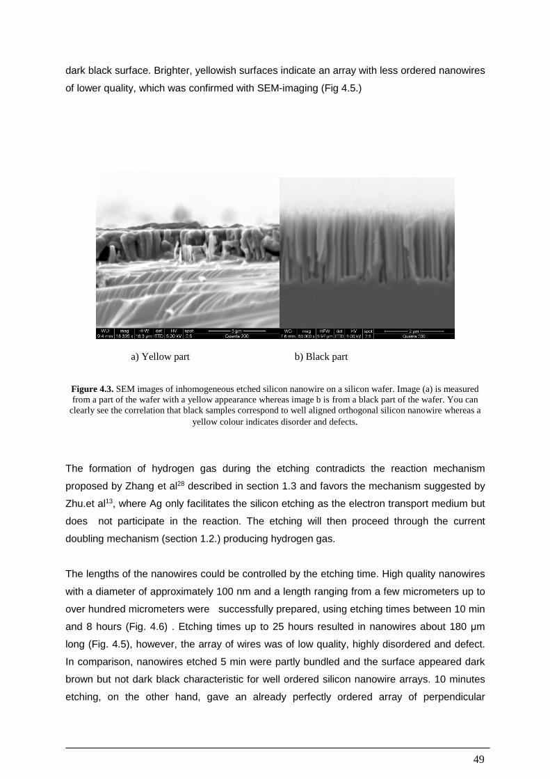
49
dark black surface. Brighter, yellowish surfaces indicate an array with less ordered nanowires
of lower quality, which was confirmed with SEM-imaging (Fig 4.5.)
a) Yellow part b) Black part
Figure 4.3. SEM images of inhomogeneous etched silicon nanowire on a silicon wafer. Image (a) is measured
from a part of the wafer with a yellow appearance whereas image b is from a black part of the wafer. You can
clearly see the correlation that black samples correspond to well aligned orthogonal silicon nanowire whereas a
yellow colour indicates disorder and defects.
The formation of hydrogen gas during the etching contradicts the reaction mechanism
proposed by Zhang et al28 described in section 1.3 and favors the mechanism suggested by
Zhu.et al13, where Ag only facilitates the silicon etching as the electron transport medium but
does not participate in the reaction. The etching will then proceed through the current
doubling mechanism (section 1.2.) producing hydrogen gas.
The lengths of the nanowires could be controlled by the etching time. High quality nanowires
with a diameter of approximately 100 nm and a length ranging from a few micrometers up to
over hundred micrometers were successfully prepared, using etching times between 10 min
and 8 hours (Fig. 4.6) . Etching times up to 25 hours resulted in nanowires about 180 μm
long (Fig. 4.5), however, the array of wires was of low quality, highly disordered and defect.
In comparison, nanowires etched 5 min were partly bundled and the surface appeared dark
brown but not dark black characteristic for well ordered silicon nanowire arrays. 10 minutes
etching, on the other hand, gave an already perfectly ordered array of perpendicular
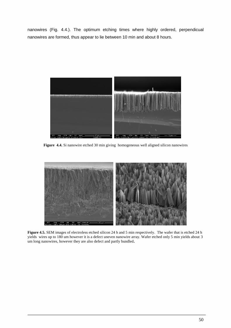
50
nanowires (Fig. 4.4.). The optimum etching times where highly ordered, perpendicual
nanowires are formed, thus appear to lie between 10 min and about 8 hours.
Figure 4.4. Si nanowire etched 30 min giving homogeneous well aligned silicon nanowires
Figure 4.5. SEM images of electroless etched silicon 24 h and 5 min respectively. The wafer that is etched 24 h
yields wires up to 180 um however it is a defect uneven nanowire array. Wafer etched only 5 min yields about 3
um long nanowires, however they are also defect and partly bundled.

51
Figure 4.6. Growth of silicon nanowire with metal catalysed chemical etching.

52
Also, the IR-transmittance of SiNWs in the mid-IR range strongly depends on the immersion
time in the HF/H2O2 etching solution. Fig. 4.7a shows typical IR transmittance spectra of
SiNW samples etched for 30 min, 60 min and 120 min, yielding nanowires with diameters
approximately 100 nm and lengths of about 20, 40 and 60 μm. The IR transmittance
decreases strongly with increasing nanowire length and falls below 2% in the mid-IR range
for 60 min etched wires. With respect to IR transmission measurements, an immersion time
of 30 min, providing about 20 μm long NWs, is the best choice in terms of spectral signal-to-
noise ratio and provides an optimum between a high-enough sample transmittance and a
sufficient sample surface area. Alternatively, IR spectra of SiNWs can als be measured in
diffuse reflection. Analogous to transmission, also the diffuse reflectivity of the silicon
nanowire array decreases strongly with etching times. Measurements of the diffuse
reflectivity from three nanowire samples etched 30 min, 1 h and 2h are shown in Fig. 4.7b.
and are quite representative for other samples.
As described in the literature91, we observe that silicon nanowires that are grown as a
disordered arrays with the VLS technique have a dull yellow appearance, indicating that a
large fraction of the incident light is reflected by scattering and not absorbed as in the case of
black, ordered nanowire arrays. Also the reflectivity of infrared light differs between ordered
and disordered NWs At 80 ° incidence angle the disordered silicon nanowire prepared via
VLS reflected very IR radiation well, more than twice as strong as a flat silicon substrate. The
reflectivity of ordered orthogonally aligned SiNWs, on the contrary, is lower than the blank
wafer.
1

53
Figure 4.7. a) Transmission spectra of silicon nanowire etched 30 min, 1h and 2h min divided by the empty
beam. b) Single beam DRIFT spectrum of nanowire etched 30 min, 1h and 2h executed at an incidence angle of
15°
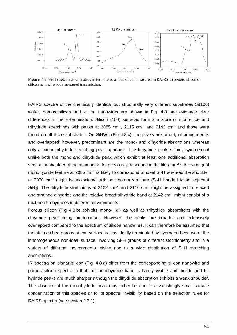
54
Figure 4.8. Si-H stretchings on hydrogen terminated a) flat silicon measured in RAIRS b) porous silicon c)
silicon nanowire both measured transmission.
RAIRS spectra of the chemically identical but structurally very different substrates Si(100)
wafer, porous silicon and silicon nanowires are shown in Fig. 4.8 and evidence clear
differences in the H-termination. Silicon (100) surfaces form a mixture of mono-, di- and
trihydride stretchings with peaks at 2085 cm-1, 2115 cm-1 and 2142 cm-1 and those were
found on all three substrates. On SiNWs (Fig 4.8.c), the peaks are broad, inhomogeneous
and overlapped; however, predominant are the mono- and dihydride absorptions whereas
only a minor trihydride stretching peak appears. The trihydride peak is fairly symmetrical
unlike both the mono and dihydride peak which exhibit at least one additional absorption
seen as a shoulder of the main peak. As previously described in the literature92, the strongest
monohydride feature at 2085 cm-1 is likely to correspond to ideal Si-H whereas the shoulder
at 2070 cm-1 might be associated with an adatom structure (Si-H bonded to an adjacent
SiH2). The dihydride stretchings at 2102 cm-1 and 2110 cm-1 might be assigned to relaxed
and strained dihydride and the relative broad trihydride band at 2142 cm-1 might consist of a
mixture of trihydrides in different environments.
Porous silicon (Fig 4.8.b) exhibits mono-, di- as well as trihydride absorpitons with the
dihydride peak being predominant. However, the peaks are broader and extensively
overlapped compared to the spectrum of silicon nanowires. It can therefore be assumed that
the stain etched porous silicon surface is less ideally terminated by hydrogen because of the
inhomogeneous non-ideal surface, involving Si-H groups of different stochiometry and in a
variety of different environments, giving rise to a wide distribution of Si-H stretching
absorptions..
IR spectra on planar silicon (Fig. 4.8.a) differ from the corresponding silicon nanowire and
porous silicon spectra in that the monohydride band is hardly visible and the di- and tri-
hydride peaks are much sharper although the dihydride absorption exhibits a weak shoulder.
The absence of the monohydride peak may either be due to a vanishingly small surface
concentration of this species or to its spectral invisibility based on the selection rules for
RAIRS spectra (see section 2.3.1)

55
Summary
The described experimental procedures allow simple and cheap preparation of oxide-free
hydrogen-terminated silicon surfaces with different topologies. Flat surfaces are simply
exposed to dilute HF solutions in order to remove the native oxide. Anisotropic oxidative
etching under formation of irregular pores were carried out in a HNO3/HF etchant solution
and high quality vertically aligned silicon nanowires were formed through Ag-catalyzed
etching in HF/H2O2. Especially the possibility to form defect free silicon nanowire arrays, at
low cost and in large scale is very interesting for new applications and it opens the field of
nanoscience to any research group having access to a chemistry laboratory. As a
consequence, we can expect a significant increase in publications dealing with silicon
nanowires for a broad range of different applications.

56
4.2. Alkylation of silicon surfaces via hydrosilylation of n-alkynes
4.2.1. Thermal hydrosilylation on planar and nanostructured silicon substrates.
As previously described in section 1.4, adsorbing an organic monolayer directly onto an
oxide free silicon surface will protect the surface against oxidation, and by attaching specific
functional groups, unique properties can be employed allowing the modified substrate to be
used in sensor18,19,30, photovoltaic51,93 or catalytic33 applications. Among a variety of methods
to attach such organic molecules to oxide free silicon surfaces under formation of a covalent
Si-C bond, the thermal-, UV- or white light initiated hydrosilylation reactions of alkynes
forming alkene monolayer or alkenes forming alkyl monolayers on H-terminated silicon
surfaces is probably the most versatile and best studied route.
In this thesis thermal hydrosilylation with alkynes were carried out. Hydrosilylation of Si(100)
surfaces is more difficult than Si(111) due to its internal roughness and its lower resistance
against oxidation. The hydrosilylation reactions is carried out at 170°C in neat alkyne and
under complete exclusion of oxygen and water in order to get a well packed monolayer.
The formation of ordered monolayers on flat silicon wafers could be confirmed by an
increase in water contact angle from about 83° to 109 ° which is in good agreement with
ordered, long-chain trichlorosilane monolayer on native silicon or thiol monolayers on gold.
Ellipsometric measurements also showed an increase in layer thickness in good agreement
with theoretically predicted values. In addition, XPS measurements showed an increase in
the carbon peak intensities and RAIRS measurements showed the characteristic CH
stretching bands known from trichlorosilane monolayers on oxide-covered silicon, namely
two positive CH2 peaks at 2920 cm-1 and 2850 cm-1 and two negative CH3 peaks at 2963 cm-
1 and 2872 cm-1.
The structure of the monolayer has been much debated, primarily whether it is an alkyl
monolayer or an alkenyl monolayer. In some studies alkenyl has been identified by a weak
infrared C=C stretching absorption around 1600 cm-194–96, other reports could not detect this
band97, either because of insufficient sensitivity or because of a follow up reaction of the C=C
double bond with a neighbour Si-H bond under the formation of a saturated double-bonded
alkyl group. We detected this C=C absorption in IR transmission spectra on high surface
area substrates such as silicon nanowires and porous silicon (fig 4.9.) but never saw it on
planar silicon wafers, most likely because of sensitivity reasons. We assume, although it
couldn’t be confirmed, that the chemistry on this substrate equals the chemistry on high
surface area substrates, forming an alkenyl monolayer upon hydrosilylation.

57
Figure 4.9 Transmission IR spectrum of H-terminated silicon nanowires before (a) and after (b) hydrosilylation
with octadecyne.
Other characteristic IR bands observed on those substrates were (CH3) at 2960 cm-1 ,
(CH2) at 2925, 2856 and (CH2) at 1465 cm-1 all confirming the formation of a hydrocarbon
adsorbate. Due to the high surface are of these substrates there is a possibility that
physisorption of the alkyne precursor is responsible for some of the CHx absorption. To
minimize the risk of such physisorption, porous silicon was sonicated in ethanol and toluene
for 5 min. Further sonication leads to no further intensity changes in the CHx bands, hence it
could be assumed that the CHx stretching bands correspond to alkyl chains covalently
bonded to the substrate through a Si-C bond. Silicon nanowires were cleaved off the
substrate upon sonication and could therefore not be cleand by sonification. Instead, they
were immersed after adsorption in ethanol and heated to 50 °C for 60 min to remove any
physysisorbed alkyne.
Both porous silicon and silicon nanowires could be characterized with transmission IR and
reflection IR. Because of the high surface roughness of both of those substrates, the incident
beam is strongly scattered after interacting with the surface, allowing Diffusion Reflection
Infrared Fourier Transformation (DRIFT) to be carried out with an optimal angle of incidence
of 15°.
Wafers recorded in DRIFT are limited to the size of the sample holder and the spectra are
often suffering from baseline shifts and other spectral artefacts. However, DRIFT is the only
applicable IR method for longer, ordered nanowires, which become intransparent for IR
radiation after an etching time of about 60 min (see Fig. 4.7). However, because nanowires
20 m long (etching time of 30 min) have a large enough surface area to obtain a satisfactory

58
SNR even from submonolayer coverages, IR transmission measurements were usually used
to follow the surface modification reactions of Si nanowires. Table 4.3. brings a compilation
of experimental results from Ellispometry, Contact Angel and RAIRS measurments for
different silicon substrates functionalized with alkyl groups of different chain lengths.
Method Si-wafer (H) Si-wafer (C18) Si-wafer (C15) Si-wafer (C12)
Ellipsometry 3 Å 21 Å 16 Å 14 Å
WCA 83° 109° 106° ------
RAIRS 2085 cm-1,
2115 cm-1,
2142 cm-1
2920 cm-1,
2850 2963 cm-1
and 2872 cm-1.
2920 cm-1, 2850
2963 cm-1 and
2872 cm-1.
2920 cm-1, 2850
2963 cm-1 and
2872 cm-1.
PSi (H) PSi (C18) SiNW (H) SiNW (C18)
FTIR 2085 cm-1,
2115 cm-1,
2142 cm-1
2920 cm-1,
2850 2963 cm-1
and 2872 cm-1.
1600 cm-1,
1400 cm-1
2085 cm-1,
2115 cm-1,
2142 cm-1
2920 cm-1, 2850
2963 cm-1 and
2872 cm-1. 1600
cm-1, 1400 cm-1
WCA 110-130° 110-130° 160-170° 160-170°
Table 4.3 Characteristics of oxide free Si(100) wafer, porous silicon and silicon nanowire before and after
hydrosilylation with octadecyne (C18), pentadecyne (C15) and dodecyne (C12).
4.2.2. Surface orientation of alkyne monolayers on Si (100) wafers
RAIRS was applied to investigate the degree of order and the surface orientation of alkyne
monolayers adsorbed on planar silicon. This information can be obtained by measuring the
CH stretching vibrations, which are extremely sensitive to the structure of the monolayer. A
high degree of structural order was confirmed by the highly anisotropic character of the
spectrum exhibiting both positive and negative peaks. The spectrum shows 2 positive CH2
peaks at 2920 cm-1 (as(CH2)) and 2850 cm-1(s(CH2)) as well as 2 negative peaks at 2963
cm-1(asCH3)), 2872 cm-1 (s(CH3)) resembling RAIRS spectra of highly ordered monolayers
of alkyltrichlorosilanes on oxidized silicon. The monolayer thickness was determined to 21 A
and the water contact angle was determined to 108 +/- 1°, both highly characteristic for an
ordered well packed monolayer.

59
3 different structure models (Fig 4.10) were utilized to calculate spectra which resemble the
experimental ones in order to determine the degree of order. In model A the monolayer is
perfectly anisotropic with ordered CH2 and CH3 groups and with the chain axis tilted by an
agle of α or -. α to the surface normal. The sign of the tilt angle has no influence on the
surface orientation of the CH2 groups. The surface orientation of the terminal CH3 groups,
however, is different for positive and negative angles. Using this model, the tilt angle of
monolayers of trichlorosilanes could earlier be determined to approximately 10°79. Model B
renders a mixture of a partly isotropic film, with an ordered well defined CH2 chain but with
the methyl groups randomly oriented, were each vibrational dipole assumes the isotropic tilt
angle of 54.7º (averaged angle over all possible spatial directions) with respect to the surface
normal. In this model the sign of the tilt angle α has no influence on the surface orientation
and on the IR absorption intensities any more. The third model is completely isotropic with no
structural order, resulting in a uniform isotropic tilt angle for all vibration dipoles.
Figur 4.10. Different structural models of monolayers of octadecyne adsorbed on silicon surfaces.
A)Anisotropic model with all-trans hydrocarbon chains. Note that the orientation of the terminal CH3 groups
depends in this case on the sign of the tilt angle . B) Mixed anisotropic/isotropic model with all-trans CH2
groups but randomly oriented CH3 chain terminal. The methyl groups orientation is independent of the value and
the sign of the chain tilt angle. C) Isotropic model with randomly oriented molecules
Figure 4.11 shows the experimental monolayer spectrum (A) in the CH stretching region of
octadecyne on a Si(100) wafer measured in Reflection Absorption Infrared Spectroscopy

60
with angle of incidence of 80° together with the calculated spectra (Figure 4.11 B-D) of a
hexadecyl group on a silicon surface for the 3 different structural models discussed above:
an all-trans geometry (model A) with a chain tilt angle of +31° (Fig 4.11B, solid line) and -31°
(Fig 4.11B, broken line), a mixed isotropic/anisotropic structure (model B) with all-trans
methylene chains tilted by 31° and disordered methyl groups (Fig 4.11 C) and a completely
disordered structure (Fig 4.11 D)
Figur 4.11 Experimental and simulated IR external reflection spectra of a high quality monolayer (d = 2.1 nm)
of octadecyne adsorbed on Si (100) (p-polarized light, 81° incidence) a) experimental spectrum b) simulated
spectrum for a fully anisotropic monolayer (model A) with a chain tilt angle of + 31° (solid line) and -31°
(broken line) c) simulated spectrum for a mixed anisotropic/isotropic monolayer (model B) with a 31° chain tilt
angle d) simulated spectrum for a fully isotropic monolayer (model C)

61
Fig. 4.11c clearly gives the best fit. The tilt angle of 31° resulting from these simulations is in
good agreement with previously reported values derived from x-ray reflectivity98, ellipsometric
film thicknesses66 or from dichroic ratios66,97–99 in ATR infrared spectra. The error margins of
these previous data have been estimated to be fairly high, whereas the infrared external
reflection spectra presented here yield an accuracy for the chain tilt angle of a few degrees,
as shown in Figure 4.12.
Figur 4.12. A) Experimental octadecyne monolayer layer spectra of five different samples with thicknesses
between 1.95 nm and 2.1 nm B) Simulated octadecyne monolayer spectra as in Fig. 4.13 c) (model B) for three
different chain tilt angles = 28°, 31° and 34°.
Figure 4.12A shows spectra of five independent samples of octadecyne monolayers, which
illustrate the reproducibility of the peak intensities in comparison to the predicted spectral
changes due to a tilt angle change of ± 3° (Fig 4.12B). Whereas the calculated spectrum for
α = 28° yields (CH2) peaks clearly stronger than in the experimental spectra, the simulated
spectrum for α = 34° shows (CH2) intensities clearly smaller than the experimental spectra.
Moreover, the (CH2) absorptions for α = 34° assume distinct derivative peak shapes, which
are caused by the increasing perpendicular component of the (CH2) transition dipoles with
increasing α, giving rise to negative peaks at slightly higher wavenumbers than the positive,
parallel component (an effect known as TO-LO splitting100). Based on the results shown in
Fig. 4.12 the alkyl group tilt angle is determined to 31± 3°.
Although a careful preparation of the monolayer films under rigorous exclusion of oxygen
normally yields high quality, ordered monolayers with very good spectral reproducibility (see
Figure 4.12A) and film thickness variations of ± 0.1 nm, lower quality films are produced from
time to time, presumably due to adventitious surface contaminations and/or partial surface

62
oxidation. Such lower quality films are often characterized by a slightly smaller film thickness
and lower water contact angles, and also show strongly altered IR reflection spectra (Fig.
4.13). In Figure 4.13 A, the spectrum of an octadecyne monolayer with 1.9 nm thickness is
shown, displaying strongly derivative-shaped (CH2) absorptions and negative (CH3) peaks.
Although derivative peak shapes are also predicted for an ordered monolayer with a chain tilt
angle > 34° (see Figure 4.12B), the more likely interpretation of the spectra in Figure 4.13 is
a film structure containing ordered and disordered domains. The experimental spectrum was
therefore fitted as a mixture of a highly ordered (model B) and a disordered contribution
(model C) and yields a very good agreement for a 74% ordered and 26% disordered ratio
(Figure 4.13A, broken line). Figure 4.13B shows another example of a more disordered
monolayer, where oxygen has been deliberately leaked into the reaction vessel to give a
monolayer of clearly diminished quality with a thickness of only 1.6 nm. Although all signs of
structural order (positive (CH2) peaks) seem to have disappeared in this spectrum, the
(CH2)/ (CH3) peak intensity ratios are considerably smaller than for a completely isotropic
film (see Fig. 4.11D) as a consequence of “hidden” positive contributions from ordered film
domains. The best fit for this spectrum is obtained for an ordered/disordered percentage of
59:41 (Figure 4B, broken line).
Fig 4.13. Experimental and simulated IR spectra of lower quality monolayers of octadecyne on Si (100). The
simulated spectra were calculated as mixtures of ordered (model B) and disordered (model C) domains: a) 74 %
ordered b) 59% ordered

63
Figur 4.14 Experimental and simulated IR spectra of high quality monolayers of a) pentadecyne (d = 1.65 nm)
and b) dodecyne (d = 1.5 nm). As in Fig. 1d), a mixed anisotropic/isotropic film structure with a 28° tilt angle of
the CH2 skeleton gave the best fit of the experimental spectra.
Fig. 4.14 shows the experimental and simulated IR reflection spectra of monolayers of 1-
pentadecyne and 1-dodecyne on Si(100). The spectra look qualitatively very similar to the
spectra of high-quality octadecyne films and show essentially identical peak maxima. Only
the (CH2) absorption intensities are reduced due to the smaller number of methylene groups
in the film molecules. An essentially identical, highly ordered structure is therefore implied
also for these shorter-chain molecules, and the best fits to the spectra are obtained for an
assumed 28° tilt angle for both compounds. The success rate of forming high-quality
monolayers with these short-chain compounds decreases and the error margins for the chain
tilt angle increases slightly to an estimated ± 5°. Structural disorder is again very clearly
indicated by a partial or complete inversion of the (CH2) absorptions (spectra not shown).
As described in section 2.3.1., the intensity of an absorption band in a reflection spectrum
can be expressed as -log Rs/R0, where Rs is the sample (substrate plus adsorbate) reflectivity
and R0 is the reflectivity of the clean substrate at the frequency of the absorption maximum
.The peak intensity depends, in addition to the orientation of the dipole moment, also strongly
on the incidence angle of the infrared beam and on the polarization direction.
For p-polarized light, the band intensities increase with increasing incidence angle while
retaining the initial band directions, until a sudden band inversion at the Brewster angle (73°
for silicon) occurs. This was observed for OTS monolayers on oxidized silicon wafers where
the negative v(CH3) as well as the positive v(CH2) bands changed direction and resulted in
identical inverted IR spectra (Fig 4.15a-b). The spectrum of a disordered film of octadecyne
adsorbed on oxide free silicon surface was also inverted upon crossing the Brewster angle:
Only negative peaks were observed above the Brewster angle (Fig 4.15c) as expected for a

64
disordered, isotropic film structure and only positive peaks were measured below the
Brewster angle (Fig 4.15d). A quite unexpected and not yet explainable result was obtained
for ordered films of octadecyne (Fig. 4.15e,f):
Figure 4.15. Experimental RAIRS spectra (solid lines) and calculated spectra (dotted lines) at 80° and 60°
incidence angle of(a-b) an ordered OTS monolayer on native silicon, (c-d) a disordered octadecyne monolayer
on silicon and (e-f) an ordered octadecyne monolayer on silicon.

65
The spectrum of ordered octadecyne at 80° incidence (Fig 4.15e) is essentiall identical to the
spectrum of OTS (Fig. 4.15a). Whereas all the peaks invert for OTS at 60° incidence (Fig
4.15b), as predicted by theory, only the CH3 peaks invert for octadecyne and the CH2 peaks
retain their positive direction (Fig 4.15f). The reason for thes discrepancies are yet unknown.
Summary
Monolayers of long-chain, terminal alkynes CnH2n+1C≡CH (n=10, 13, 16) yield highly ordered
structures with a uniform chain tilt angle, if prepared under optimized experimental conditions
under rigorous exclusion of oxygen. External reflection IR spectroscopy in combination with
spectral simulation routines yield tilt angles of 31±3° for octadecyne (n=16) and 28±5° for
pentadecyne (n=13) and dodecyne (n=10) monolayers. Lower-quality films with often
unchanged ellipsometric film thicknesses yield markedly different IR spectra, which could be
identified as due to mixtures of ordered and disordered film domains and allow a quantitative
evaluation of the degree of disorder.
In general, monolayers of alkynes on Si(100) surfaces seem to be less ordered than silanes
on silica or thiols on gold because the terminal CH3 groups of alkyne monlayers are randomly
oriented in contrast to the othe systems. One possible reason for this could be the surface
roughness of about 3 Å of hydrogen terminated Si(100) as opposed to the perfectly flat,
oxide-covered Si(100) substrate. Another possible reason is the stability of the Si-C bond
(Si-C bond energy 4 eV compared to 0.11 eV45 for Au-S bonds of thiols on gold). Although
stable monolayers are desirable because of more robustness against oxidation and heat, it is
also much harder for such strongly bound molecules to rearrange on the surface and pack
into a oriented, highly ordered structure.

66
4.2.3 Wetting properties of alkyl modified silicon substrates
The influence of surface porosity on wetting properties Fig 4.16 shows contact angle measurements on a silicon wafer, porous silicon and silicon
nanowires, which exhibit interesting trends and differences between these substrates and
demonstrate a pronounced influence of the surface porosity and the surface composition
(coating) on the wetting properties. The water contact angle on flat hydrogen terminated
silicon was determined to slightly above 80°, which is under the critical angle of 90°. This
means that structured silicon surfaces following the Wenzel model will exhibit a decrease in
water contact angle compared to flat silicon surfaces (see Fig 2.4). This is, however not
observed experimentally, instead, the water contact angle increased to 130° on hydrogen
terminated porous silicon and further up to 170° on hydrogen terminated silicon nanowires.
Thus, silicon nanowires exhibit what is called “superhydrophobic” properties, i.e. water
contact angles > 150°. This increase of an initially hydrophilic contact angle < 90° of the flat
substrate into the hydrophobic (>90°) or superhydrophobic (>150°) regime can only be
explained by a Cassie-Baxter type wetting (see Fig. 2.5), although a transformation from the
Cassie-Baxter state to the Wenzel state normally occurs for θ<90°. Coating the substrates
with octadecyne, results in an increase in water contact angle on flat silicon substrate from
80° to 109°. Nanostructured silicon, however, gave essentially the same contact angles for
the uncoated (H-terminated) and the octadecyne-coated substrates. This indicates that
among the two major factors determining the wetting properties – chemical composition and
surface morphology – the latter one is completely dominating in the systems studied here.
Figure 4.16. Illustration of how roughening the surface influences the contact angle on flat silicon, porous
silicon and silicon nanowires coated with octadecyne.

67
In addition to water, the contact angle of ethyleneglycol was also measured on the different
substrates (Fig 4.17a). Ethyleneglycol is less polar and the water contact angle on hydrogen
terminated flat silicon surfaces was distinctly lower, approximately 60°. Roughening the
surfaces resulted, contrary to the water contact angles, in a decrease in water contact angle
on porous silicon to less than 40° and full wetting (θ<10°) on silicon nanowires, as predicted
by the Wenzel wetting model (Fig 2.4). Thus, Cassie-Baxter wetting for water changes to
Wenzel wetting for ethylene glycol on hydrogen-terminated silicon substrates.
On coated flat silicon surfaces the WCA of ethylene glycol increases to 79°. On porous
silicon this angle decreases to slightly above 72°, thus still exhibiting Wenzel wetting
properties. On silicon nanowires, in comparison, the WCA increases up to 150° in
accordance with the Cassie-Baxter model. Thus, it seems that there is some critical contact
angle θc around 70° on flat surfaces, where the wetting of the corresponding structured
substrates changes suddenly from Wenzel-type for θ<θc to Cassie type for θ>θc.
Fig 4.17b shows the contact angles as a function of the porosity for hydrogen-terminated and
octadecyne-coated silicon substrates with water and ethylene glycol. The porosity of flat
silicon is 0 and the porosity of silicon nanowires is assumed to be close to 1 as water contact
angles over 170°C are measured (see Fig. 2.5). The porosity of porous silicon is assumed to
be somewhere around 0.4 and probably varies quite aubstantially from sample to sample as
the etching is not completely reproducible.
Porous silicon has a critical angle of slightly less than 80°, where a transition to the Wenzel
state occurs and roughening results in θ < θc. On silicon nanowires, this critical point is
lower, somewhere between 60° and 77° as judged from the increase in ethylene contact
angle on the octadecyne-coated substrate and a decrease on the hydrogen-terminated
substrate. It can be assumed that the Cassie-Baxter wetting on porous silicon is harder to
maintain compared to silicon nanowires with their very small, sharp needle array, having a
greater amount of air under the water droplet. Hence porous silicon reaches the critical point,
where a transition between the Cassie-Baxter state to the Wenzel state occurs, earlier than a
nanowire array.
From the contact angle measurement with water and ethyleneglygol could thereby be
confirmed that the hydrosilylation reaction indeed take place on all three substrates. The
surface free energy of hydrogen terminated and coated flat silicon were subsequently
determined by the method of Owens–Wendt–Rabel-Kaeble (OWRK) confirming a
significantly lower surface energy of coated flat silicon substrate, 22 mN/m compared to 48
mN/m on the hydrogen terminated surface.

68
a)
b)
Figure 4.17 a) Contact angle of water and ethylene glycol on H-terminated and octadecyne-coated silicon
substrates. b) same as a) but drawn as a function of substrate porosity

69
4.2.4. Oxidation of bare and alkylated silicon surfaces
Oxidation in ambient atmosphere
The hydrosilylation reaction competes with the much faster surface oxidation, hence for
successful attaching of organic monolayers, a strict moisture- and oxide-free environment is
demanded. Bare, hydrogen-terminated silicon surfaces are not stable for more than 10-15
minutes in air and form a native oxide layer 10-15 Ångström thick, hence non-reacted Si-H
sites of the initial surface will oxidize..
Time (hours)
0 2 4 6 8 10 12 14 16 18 20
Wa
ter
Co
nta
ct
An
ge
l(º)
40
60
80
100
120
140
160
180
SiNW-C18
SiNW-H
PS-C18
PS-H
Flat-C18
Flat-H
Figure 4.18 Contact angle measurements of H-terminated and octadecyne coated silicon substrates exposed to
60°C in an oven
Contact angle measurements were used to monitor the rate uf surface oxidation on
hydrogen-terminated and octadecyne-coated silicon substrates (silicon wafers, porous silicon
and silicon nanowires). The polar surface oxide decreases the water contact angle drastically
in comparison to a H-terminated or an alkyl-covered surface, and therefore the contact angle
is a rather sensitive parameter for the extent of surface oxidation. The results of these

70
measurements are shown in Fig. 4.18. A temperature of 60°C was chosen in order to
accelerate the rather slow oxidation of H-terminated silicon surfaces. It can be seen clearly
from Fig. 4.18, that the octadecyne coating provides an excellent protection against surface
oxidation for all three types of substrates, whereas the uncoated, H-terminated surfaces
oxidize rapidly under the conditions of these experiments.
Oxidation in basic solution
Hydrogen terminated silicon surfaces are quite unstable in aqueous basic solutions101. When
exposed to alkaline solutions, they are etched according to the following reaction.
Si + 2H2O +2OH- [Si(OH)2O2]2- + 2H2
Chemical etching initiated by OH- attack is highly anisotropic, however, in contrast to etching
in fluoride solutions where electron holes are directed to pore holes favouring etching,
etching in alkaline solutions is a thermally activated process and occurs essentially only at
step edges. Thereby, initiation by hydroxide attack leads to the production of atomically flat
surfaces , which is used in a process called chemically polishing of silicon wafer surfaces.
Here, the stability of H-terminated and octadecyne-coated Si nanowires in aqueous NaOH
solution of pH 12 was investigated by secondary electron microscopy. Fig. 4.19. shows SEM
images of uncoated and coated SiNWs after different immersion times in the basic solution.
H-terminated silicon nanowires are completely etched away already after 1 h exposed to
NaOH with only some stumps remaining. Those stumps are also etched away after longer
exposing times forming a flat surface. However, silicon nanowires coated with an octadecyl
monolayer prevail the attack of the hydroxyl group and the nanowires are intact and
essentially unchanged even after 12 h exposure.

71
Figur 4.19. Stability of coated and uncoated silicon nanowire in alkaline solution (R.T. pH12)
Summary
Interesting differences in the wetting properties of the H-terminated and alkyl-coated silicon
substrates were observed as well as the great influence of the surface roughness on the
wetting properties. The critical contact angle where a transition between the Cassie state and
the Wenzel state occurs on structured surfaces was found here as low as about 78°. This is
an interesting and unexpected result as it is normally believed that a Cassie state can only
occur for an intrinsic contact angle (also called θ flat ) larger than 90°. There are, however, a
few reports in the literature dealing with superhydrophobic surfaces with intrinsically
hydrophilic properties (θflat<90°), where the surface consists of micro textures with so-called
overhang structures102. One example of such a surface is the well known superhydrophobic

72
lotus leave35. On the nanowires prepared in this thesis, however, such a topology was not
aimed for and the SEM images show straight, vertical nanowires. Thus the
superhydrophobicity observed with these samples cannot be explained by such overhang
structures. Another interesting, future aspect of these studies is the construction of
superoleophobic surfaces, i.e. surfaces which repel water but also oils and hydrocarbon
solvents. Whereas superhydrophobis surfaces are quite common in nature, for example the
already mentioned lotus leave, the water strider legs, a special kind of butterflie`s wings and
other plant leves, there is no natural superoleophobic surface known and also synthetic
examples are rare, because it is not clear yet what makes a surface superoleophobic. In light
of some very promising applications, e.g. for stain resistant materials or for oil-water
separation, one can expect consolidated research efforts in this field in the near future
Another interesting result of the studies described in this chapter is the very efficient
protection of silicon nanowires against corrosion in alkaline solution. Also this can be
expected to be of practical importance for the protection of SiNW based devices like field
effect transistors or solar cells.

73
4.3. Adsorption of activated alkynes
4.3.1. Propiolic acid mono- and diesters
Liu et. al103 recently presented a mild and efficient Si (111) surface modification procedure
via hydrosilylation of activated alkynes such as propiolate esters, propiolic acid, but-3-yne-2-
one, propiolnitrile and phenylacetylene. The very mild reaction conditions inspired us to
investigate this approach further on flat silicon, porous silicon and silicon nanowires.
The silicon substrates were modified with 3 different terminal propiolate esters, a longchain
monoester (tetradecanolpropiolate, TDP), a longchain diester (decadioldipropiolate, DDDP)
and a short chain diester (ethanediol dipropiolate, EDDP). Si(100) wafers were first exposed
to neat DDDP under Ar atm at 170°C . However, DDDP was fully polymerized to a solid
polymer under these conditions, precluding this condition for monolayer adsorption. To avoid
polymerization, the esters were therefore adsorbed in solution (0.2 M in mesitylene) at lower
temperatures.
Figure 4.20. RAIRS spectra of tetradecanolpropiolate (solid line) and pentadecyne (dotted line) adsorbed on a
Si(100) wafer
Tetradecanolpropiolate was attached via hydrosilylation to a Si(100) wafer surface under
relatively mild condition (120 °C, 15 h). The RAIRS spectrum shown in Fig. 4.20 resembles
the spectrum of a pentadecyne monolayer with 2 positive CH2 peaks at 2920 cm-1 (as(CH2))
and 2850 cm-1(vs(CH2)) as well as 2 negative peaks at 2963 cm-1(asCH3)) and 2872 cm-1
(s(CH3)). The monolayer formed from the activated alkyne clearly has an ordered structure
similar to adsorbed n-alkynes as judged from the anisotropic character (positive and negative
peaks) of the RAIRS spectrum. The weaker peak intensities and the slightly distorted peak
shapes, however, indicate a slightly lower surface coverage and a partly disordered film
structure compared to n-alkyne monolayers. This might be due to steric reasons caused by

74
the bulky terminal ester group. The different adsorption conditions (0.2 M solution at 120°
instead of neat alkyne at 170°) might further hamper the formation of a perfect ordered
monolayer,Other characteristic IR vibrations such as the C=O stretching at 1700 cm-1 and
the C=C absorption at 1600 cm-1 couldn’t be detected, presumably because of insufficient
sensitivity.
Subsequently, the 2 diesters DDDP and EDDP were in the same manner adsorbed onto a
Si(100) wafer. Their shorter chain lengths and diminished peak intensities, however,
precluded a characterization with RAIRS. A different, more sensitive IR technique –
attenuated total relfection (ATR) – was therefore employed. The ATR spectra of TDP, DDDP
and EDDP are shown in Fig 4.21b and evidence the successful adsorption of all 3
compounds on the polycrystalline Si surface of the ATR element. The TDP spectrum shows
the CH2 peaks at 2925 cm-1 (as(CH2)) and 2855 cm-1(s(CH2)) as well as a peak at 2963 cm-
1 (asCH3)). The wavenumbers are slightly shifted compared to TDP adsorbed on a Si(100)
wafer, which indicate a less ordered monolayer film. One possible reason for these
differences might be the significantly larger amount of solvent necessary for the adsorption,
on the ATR crystal (20 mL compared to 3 mL), which might introduce additional oxygen and
contaminate the surface. The C=O stretching region in the ATR spectra of Fig. 4.21b is,
unfortunately, shadowed by a strong intrinsic absorption of the ATR crystal and does
therefore not allow any conclusive band assignments in this region. The ATR spectra of
DDDP and EDDP in Fig. 4.21b show in addition to the (CH2) absorptions the (C≡C)
stretching band at 2121 cm-1 of the terminal alkyne group. The terminal (H-C) absorption,
which is expected around 3260 cm-1, is not detected, presumably due to lack of sensitivity.
The mono- and dipropiolate esters were further adsorbed onto porous silicon and on silicon
nanowires to achieve information on how the surface morphology influences the adsorption
Transmission FTIR measurements of TDP adsorbed on silicon nanowires clearly evidenced
a successful adsorption (Fig 4.21a). In addition to the CH2 and CH3 absorptions that could be
detected also on Si(100) wafers, the ester (C=O) peak at 1726 cm-1. and the CH2
deformation mode at 1451 cm-1 were assigned. Also, successful adsorption of the diesters
DDDP and EDDP on Si nanowires could be derived from the IR spectra in Fig 4.21a, which
show absorptions of the terminal alkyne groups of adsorbed DDDP and EDDP at 3263 cm-1
((H-C)) and 2121 cm-1 ((C≡C)) as well as the ester (C=O) peak at 1726 cm-1. The CH2
absorptions appear below 3000 cm-1 and the CH2 deformation mode at 1451 cm-1. The ratio
A(C=O)/A(CnH2n/n) where A(C=O) is the integral of the C=O peak and A(CnH2n/n) is the
integral of the CH stretching peak divided by the number of carbon atoms, is approximately
twice as large for DDDP (4.8) compared to TDP(2.3) as expected due to the second carbonyl
group of the diester.

75
Figure 4.21 IR spectra of different silicon substrates modified with TDP, DDDP and EDDP a) silicon nanowires
b) flat polycrystalline silicon (ATR crystal) c) and porous silicon.

76
IR spectra of the propiolate esters adsorbed on porous silicon are shown in Fig 4.21c. The
spectrum of adsorbed TDP resembles the spectrum of TDP on nanowires with a ratio
A(C=O)/A(CnH2n/n) of 2.6. The DDDP and EDDP spectra on porous silicon differ, however,
clearly from the other substrates and do not show the characteristic alkyne peaks at 3263
cm-1 ((H-C)) and 2121 cm-1 ((C≡C)). The latter would also be hard to detect because of
strong Si-H stretchings in this region. The C=O peaks is present at 1725 cm-1 and the
(C=O)/A(CnHn-1/n) is 4.8, i.e. again – as on Si nanowires - approximately twice as large as
adsorbed TDP, indicating that the diesters were successfully attached onto porous silicon
surfaces although the terminal alkyne group could be detected in the IR spectra. A possible
explanation could be that that the inhomogeneous morphology and concave surface
geometry of porous silicon enables the diynes to bind with both terminal alkyne groups to the
substrate. This is illustrated in Fig. 4.26 and will be discussed in more detail later.
4.3.2. Reversible acid-base surface reactions of adsorbed propiolic acid.
Recently Imanishi et.al104 reported on reversible acid-base surface reactions on oxide free
Si(111) surfaces modified with α,β-unsaturated carbonyl compounds via hydrosilylation, As
electron deficient alkynes are more reactive and allow the hydrosilylation reaction to be
carried out under more moderate conditions, propiolic acid or acrylic acid and its derivatives
are interesting precursors to functionalize silicon surfaces under mild conditions. By treating
the carboxylic acid terminated surface alternatively with acid and alkaline solution, it was
possible to reversibly transform this functionality between the acid and the acid salt. Transfer
between the acid and the salt of the adsorbed film will potentially change the electronic
properties (e.g. the conductance) of the silicon substrate and, hence allowing it to be as a
simple sensor or switch. This study inspired us to try this approach for the functionalization of
Si nanowires and porous Si. Figure 4.22 a) shows the resultant transmission spectrum of H-
terminated porous silicon exposed to a 0.5 M propiolic acid/mesitylene solution for 12h at
120 °C. The peak at 1719 cm-1 is assigned to the C=O vibration of the COOH group
confirming that propiolic acid was attached to the Si surface, mainly in its acid form, however
a weak band at 1560 cm-1 indicated that a minor part was ionized..

77
Wavenumber (cm-1)
1400150016001700180019002000
Ab
so
rba
nce
-0,02
-0,01
0,00
0,01
0,02
0,03
0,04
0,05
0,06
C=C
C=O (COOH)
C=O (COO-)
1725
1575
a)
b)
c)
Figure 4.22 IR transmission spectra of porous silicon coated with propiolic acid a) spectrum of a freshly coated
substrate b) after rinsing in 0.01 NaOH solution. c) after further rinsing in 2.0 M HCl solution.
The small peak at 1605 cm-1 assigned to the C=C bond indicates that propiolic acid is
attached to the Si surface via hydrosilylation of the alkyne group and not through a side
reaction of the carboxylic group. The spectrum of the Si surface after rinsing in 0.01M NaOH
solution is shown in Figure 4.22b. The major absorption appears at 1575 cm-1 and is
assigned to the (COO-) stretching vibration of the carboxylate group, indicating that the
carboxyl group is ionized to its corresponding salt in alkaline solution. Exposing the alkali-
treated substrate to 2.0 M HCl solution results in the disappearance of the 1575 cm-1 salt
and regeneration of the original 1719 cm-1 absorption of the undissociated carboxylic acid.
A monolayer of propiolic acid adsorbed on porous silicon therefore allows reversible
switching between the acid and the basic form of the surface acid groups. .
Propiolic acid functionalized porous silicon substrates were subsequently placed in an oven
heated to 170 °C in order to explore the thermal stability of the acid monolayer. Fig 4.23.
shows the IR spectra monitoring potential thermally induced damage to the monolayer.

78
Figure 4.23 IR spectra of propiolic acid adsorbed on porous silicon and annealed at 170°C for different times. a)
freshly adsorbed propiolic acid b) after 5 min at 170 °C c) after 30 min at 170 °C d) after 16h at 170 °C e) after
7 days at 170 °C f) after subsequent exposure to 0.01 M NaOH g) after subsequent exposure to 2M HCl
Exposing the substrate for 7 days did not result in any decrease in the intensity of the acid
carbonyl peak.. However, the peak maximum shifted from 1719 cm-1 continuously to 1735
cm-1 after one week exposure, whereby a shift of 6 cm-1 was already observed after 5
minutes at 170°C. Subsequent rinsing with 0.01 M NaOH generated a carboxylate salt peak
(COO-)at 1576 cm-1 and further rinsing with 2M HCl regenerated the 1725 cm-1 acid peak
in complete analogy to the freshly adsorbed, not heated samples. This shows that the
chemical properties of this propiolic acid monolayer are unchanged even after one week at
170°. It also demonstrates the very high chemical and thermal stability of these Si-C bonded
monolayers. The high wavenumber shift of the C=O peak with increasing high temperature
exposure might be explained by an initial H-bonded structure of the freshly prepared sample,
which is successively destroyed at higher temperatures, shifting the C=O peak maximum to
higher wavenumbers.
Propiolic acid were subsequently adsorbed on silicon nanowire transistors. The idea was that
the electron withdrawing oxygen of the carboxylic group will through charge transfer
influence the conductivity of the silicon nanowire in a similar way as conventional doping.

79
Attaching a carboxylic acid would potentially allow tuning the electric properties of the silicon
nanowire with the pH level.
For this purpose, silicon nanowire transistors were fabricated, containing two Ni contact
connected with a Si nanowire allowing the Si nanowire conductance to be measured. The
transistors were treated according to the modification procedure described, oxide etching in
5% HF followed by hydrosilylation 0.5 M propiolic acid in mesitylene at 120 °C and the
electric properties were subsequently measured. Unfortunately modified nanowires did not
conduct any current and the reason for this was clear after comparing SEM pictured of the
Figure 4.24. Silicon nanowire transistors before and after treatment with 5% HF
transistors before and after the functionalization, Fig. 4.24a shows two nickel contacts
connected with a silicon nanowire and fig 4.23b shows the same transistors after being
treated with 5% HF. The Ni-Silicide contacts are clearly etched away precluding conductance
measurements. In order to avoid such as etching, the Ni-Silicide might be protected with a
PMMA photo-coating prior to the modification, alternatively the nanowires could be
functionalized prior to the fabrication of the transistor.

80
4.4. Surface functionalization via click chemistry
4.4.1. Copper-catalysed Huisgen cycloadditions
Adding functional groups to the silicon surface is of major importance for practical
applications, as mentioned before. This can be carried out in one step, by hydrosilylation with
an alkyne carrying the desired terminal functionality, as described in the previous section.
However, attaching complex molecules in one step has several drawbacks. One is the time
and potential difficulties involved in synthesising the molecule, more important, however, is
the often encountered incompatibility between the desired functionalities and the attachment
procedure. The desired functionalities must be robust enough to survive the rather harsh
reaction conditions of hydrosilylation, such as high temperatures up to 170°C or UV
irradiation. Moreover, the desired functionalities may react with the silicon hydride surface
which has a broad reactivity spectrum and, besides the hydrosilylation reaction with
unsaturated hydrocarbons, has been reported to react with halogens, nitriles, alcohols,
aldehydes, and ketones52. Hence, it is often a better strategy to immobilize the functionalities
onto silicon surfaces in a two-step attachment procedure where a primer layer containing a
compatible reactive terminal functionality is covalently attached to the surface and the
desired functionality is then added in a subsequent coupling reaction with the primer layer.
One of the most versatile and reliable coupling reactions for this purpose is the copper
catalysed Huisgen cycloaddition between an azide and an alkyne, forming a triazole ring in
often quantitative yields without any side products. This reaction has proven its versatility and
efficiency for surface modifications of a broad range of solid substrates, including oxide-free
silicon83,85,105–107 and is compatible with a wide range of functionalities. In order to test how
the surface morphology affects this modification strategy, this reaction was applied using
porous silicon and Si nanowires as substrates.
As described in the experimental section, porous silicon and silicon nanowire substrates
were modified with an acetylene terminated monolayer (1,8 nonadiyne), which was
subsequently coupled via a Cu(I)-catalyzed Huisgen 1,3-dipolar cycloaddition reaction (click
reaction) with an organic azide R-N3 The course of this surface click reaction was followed in
the infrared spectra (Fig. 4.25) and yielded some pronounced differences between porous Si
and Si nanowires as the substrate. The major absorptions in the spectra of the nonadiyne
primer layer shown in Fig. 4.25 are the CH2 stretching absorptions at 2860 and 2930 cm-1
and the terminal ( H-C≡C) band at 3322 cm-1. Upon coupling, the ( H-C≡C) band is
strongly reduced or disappears completely, the (CH2) bands increase and an additional

81
shoulder at 2960 cm-1 assigned to (CH3) of the coupled octyl group appears. The peak
intensity ratio (H-C≡C)/(CH2) in the nonadiyne monolayer spectra was about half on
porous silicon (0,08+/-0,03) compared to silicon nanowires (0.16 +/- 0,03), indicating a
substantially reduced surface concentration of free, terminal alkyne groups on porous silicon.
Moreover, the acetylene-terminated silicon nanowire surface couples quantitatively with
azidooctane as judged from the complete disappearance of the (H-C≡C) absorption at 3323
cm-1, whereas a residual (H-C≡C) is seen from unreacted nonadiyne in the spectrum on
porous silicon after coupling. Accordingly, the the intensity gain of the (CH2) absorptions
upon coupling is also much smaller – slightly less than half – on porous Si compared to Si
nanowires. The overall surface concentration of coupled azide is therefore estimated to be
less than 50% on porous Si compared to Si NWs.
Wavenumber (cm-1
)
2800300032003400
Ab
so
rba
nce
-0,02
0,00
0,02
0,04
0,06
0,08
0,10
0,12
0,14
0,16
CuSO4
C8H17N3
EtOH/H2O
Wavenumber (cm-1
)
2800300032003400
Ab
so
rba
nce
-0,05
0,00
0,05
0,10
0,15
0,20
0,25
Figure 4.25. IR spectra monitoring the copper catalysed click reaction between 1,8 nonadiyne coated porous
silicon (dashed line) and silicon nanowires (solid line) and 1-azidooctan
Similar results of a substantially reduced surface alkyne concentration on porous silicon
compared to Si NWs were obtained with the propiolic acid dieseters DDDP and EDDP
(section 4.3.1) We therefore postulate here again that the inhomogeneous morphology and
concave surface geometry of porous silicon might enable diynes to bind with both terminal
alkyne groups to the substrate, as shown schematically in Fig 4.26, rendering these
molecules unreactive in the subsequent click coupling step. This interpretation is also

82
supported by a substantially higher (C=C)/ (CH2) ratio in the nonadiyne monolayer spectra
on porous silicon compared to silicon nanowires ((C=C) is the absorption around 1600 cm-1
due to surface-bound alkenyl groups. Moreover, some of the surface alkyne groups might be
inaccessible to the azide due to steric reasons, resulting altogether in a strongly reduced
reaction yield on porous silicon.
Figure 4.26. Schematic illustration nonadiyne adsorbed on porous silicon and silicon nanowires. The
inhomogeneous morphology and concave surface geometry of porous silicon enable diynes to bind with both
terminal alkyne groups to the substrate
4.3.2 Copper-free click reactions
Although the copper-catalysed Huisgen cycloaddition is an easy and reliable way to
postfunctionalize silicon surfaces with desired groups, the use of copper is a major obstacle
and might cause problems in various applications. Traces of copper are known to retain on
the surface despite copious rinsing in EDTA and thereby alter the electronic properties of the
substrate dramatically108. In biological environments copper is often precluded because of its
cytotoxic properties109. Copper is also known to cause degradation of DNA molecules110 and
to induce protein denaturation111.
One alternative solution to bypass the problem caused by copper would be to design a
surface with terminal electron deficient alkynes, formed by adding an electron withdrawing
group on the gamma carbon atom. Such electron deficient alkynes are known to react with
azides in the absence of copper, whereby the surface is turned into a clickable platform,
which can, without any additives, be coupled with an over layer of an organic azide carrying
the desired terminal functionality. Although such a metal free postfunctionalization strategy of
surfaces would obviously be highly preferable, this topic is to date still rather unexplored.
This motivated us to explore this approach, aiming a reliable, robust functionalization
procedure that allows attachment of functional groups onto oxide-free silicon surfaces under
mild conditions without the addition of a metal catalyst

83
SiNWs about 20 μm long and 80 nm thick were prepared as previously described and
subjected to the following surface modification procedure shown schematically in Fig. 4.27:
In the first step, the native oxide layer is removed by HF, forming a hydrogen-terminated
surface. The next step is a hydrosilylation reaction forming a clickable anchor layer. To form
this anchor layer we chose 1,2-ethanediol dipropiolate (EDDP). It is a short chain, activated
dialkyne, easy to synthesize and, as shown in chapter 4.3, can be successfully attached to
silicon nanowires. The electron withdrawing carbonyl groups are known to activate the
terminal alkyne groups, which brings two important advantages for the purpose of this study:
First, such activated alkynes are more reactive for hydrosilylation103 such that the primer
layer formation can be carried out under milder reaction conditions. Second, the subsequent
surface click coupling via cycloaddition of an azide can be carried out without copper
catalysis. Thus, in summary, this compound EDDP is a promising precursor for the
functionalization of silicon surfaces under mild and catalyst-free conditions. The last step of
this modification procedure was then the click coupling of the EDDP primer layer with
octylazide, which was carried out in by immersion of the EDDP-primed SiNW substrate in a
0.5 M solution for 6 h in ethanol (toluene or DMSO can also be used as solvents
alternatively).
Figure 4.27. Water contact angles and infrared spectra of surface-modified silicon nanowires:(a) hydrogen-
terminated SiNW, (b) after hydrosilylation of (a) with 1,2-ethanediol dipropiolate, and (c) after click reaction of
(b) with 1-azidooctane.

84
The course of this surface modification process was followed with infrared spectroscopy.
Starting with a H-terminated Si surface (Figure 4.27a) with its characteristic –SiHx (x = 1, 2,
3) stretching vibrations at 2142 cm-1 (SiH3), 2110 cm-1 (SiH2) and 2087 cm-1 (SiH) , these
bands disappear completely upon adsorption of EDDP (Figure 4.27b) and are replaced by
absorptions of the terminal alkyne groups of adsorbed EDDP at 3263 cm-1 ((H-C)) and 2121
cm-1 ((C≡C)) as well as the ester (C=O) peak at 1726 cm-1. The alkyne ((H-C)) absorption
is unusually broad and is shifted by almost 50 cm-1 to lower wavenumbers compared to
adsorbed 1,8 nonadiyne. The CH stretching absorptions of EDDP appear below 3000 cm-1
and the CH2 deformation mode at 1451 cm-1. Clicking 1-azidooctane onto this EDDP
monolayer (Fig 4.27c) results in the disappearance of the alkyne (H-C) and (C≡C) peaks
and the growth of the (CH) and (CH2) absorptions of the octyl group at 2960cm-
1(as(CH3)), 2930 cm-1 (as(CH2)), 2859 cm-1 (s(CH2)) and 1455 cm-1 ((CH2)). A small peak
at 3142 cm-1 is presumably the (H-C=C) stretching absorption of the single CH group in the
triazole ring. The (C=O) absorption shifts from 1726 cm-1 to 1734 cm-1 upon click coupling.
This high frequency shift, together with the broad, low-frequency absorption of (H-C≡C) of
adsorbed EDDP in Fig 4.27b, indicates a hydrogen bonding interaction between the alkyne
hydrogen and the ester carbonyl group in the EDDP layer, which weakens both the alkyne H-
C bond and carbonyl bond and causes a low frequency shift of their stretching absorptions.
The click reaction removes the alkyne hydrogen and (C=O) shifts back to higher
wavenumbers in the click product (Figure 4.27c). A blind experiment – exposure of the EDDP
monolayer to pure solvent under the same conditions as in the click reaction – yielded an
unchanged EDDP monolayer spectrum. Under the current reaction conditions (6h exposure
at 50°C), the yield of the surface click reaction is essentially quantitative as judged from the
complete disappearance of the terminal alkyne absorptions. Another indication of successful
surface modification could also be achieved by following the changes in wetting properties in
the course of this modification. H-terminated silicon nanowire surfaces have
superhydrophobic wetting properties as a consequence of both structural and chemical
factors (see section 4.2.3) with water contact angels of 150-170º depending on the surface
morphology. Adsorbing the highly polar EDDP changes the chemical properties and results
in a superhydrophilic surface with a water contact angle less than 10°, which upon coupling
with azidooctane rises again to about 115º. This latter result is interesting in the sense that
densely packed hydrocarbon monolayers on SiNWs have been shown to yield
superhydrophobic properties with WCAs of 170° (see. 4.2.3) . After click coupling here, the
SiNWs should also be covered by a hydrocarbon layer albeit with a somewhat shorter chain
length (octyl) than the octadecyne monolayers described in 4.2.3. The measured contact
angle of 115° suggests that the octyl layer after click coupling is not as perfect and densely
packed as the octadecyl layer adsorbed directly. This is further supported by results for an

85
incomplete click coupling reaction with only 2h reaction time at 50°C, after which a WCA of
only 90° was measured.
Non-activated alkyne
H-C≡C-(CH2)7-C≡C-H
Activated alkyne
H-C≡C-OOC-(CH2)2-COO-C≡C-H
Figure 4.28. Click reaction of activated and non-activated alkynes adsorbed on Si nanowires with 1-azidooctane
No reaction occurred when the non-activated 1,8-nonadiyne was adsorbed and exposed
under the same reaction conditions to the click reagent 1-azidooctane (Fig. 4.28). Only in the
presence of a Cu-catalyst, this latter reaction proceeded quantitatively as shown in Fig. 4.28
and described in more detail in the previous chapter. This proves the importance of an
electron withdrawing group at the γ-carbon for successful cycloadditions to be carried out
under moderate conditions.
The modification protocol described above was used to attach different functional groups to
the silicon nanowires such as phenyl, nitrile and azide (Fig.4.29) . Coupling 1.2-
diazidoethane onto the EDDP anchor layers, for example, forms a new clickable platform of
an azide terminated surface allowing a second cycloaddition with a terminated alkyne - a so
called tandem click reaction - to be carried out. The coupling reactions shown in Fig. 4.29
were equally successful carried out in ethanol, toluene, THF and DMSO, showing that this
reaction can be carried out in polar as well as nonpolar solvents. This is another great
advantage of this copper-free modification strategy compared to the copper catalyzed
version, which, according to previous studies, gave rather poor yields in nonpolar solvents
because of insufficient solubility of the Cu catalyst112. To be able to carry out the coupling
in nonpolar solvents is obviously a great advantage when attaching large nonpolar molecules

86
like long-chain hydrocarbon compounds, which are insoluble in the standard H2O/EtOH
solution commonly utilized for the copper catalysed click reaction. Moreover, the silicon
substrate may be more resistant to oxidation in nonpolar solvents compared to polar solvents
because of their generally lower O2 solubilities.
Figure 4.29. Surface click coupling of different target functionalities onto silicon nanowires primed with
ethandiol dipropiolate (EDDP)

87
The surface modification procedure was also successfully carried out on planar Si. Due to
the limited sensitivity of RAIRS, the modification was followed by ATR as shown in Fig 4.30.
The surface in this case is a polycristalline silicon surface and certain spectral differences in
band shapes and peak positions compared to Si(100) as a substrate must be ascribed to the
different surface crystal structure. Starting with the hydrogen-terminated surface yielding a
broad band at 2100 cm-1-2190 cm-1(Fig. 4.30, upper spectrum), the SiHx band disappears
as on silicon nanowires upon adsorption of EDDP and is replaced by a sharp (C≡C)
stretching absorption at 2120 cm-1 (Fig. 4.30, middle spectrum), which upon exposure to 1-
azidooctane at 50 °C completely vanishes.(Fig. 4.30, lower spectrum). As the ATR crystal
absorbs radiation slightly above 1700 cm-1, an analysis of the C=O stretching absorption
was prohibited. The triazole absorption at 3142 and the (C=C) stretching band around 1600
cm-1 could not be detected, presumably because of insufficient sensitivity. .
Figur 4.30. Infrared spectra of surface-modified silicon ATR crystals. Top: a hydrogen-terminated ATR crystal.
Middle: after hydrosilylation with 1,2-ethanediol dipropiolate Bottom: after click reaction of with 1-azidooctane.
As mentioned in chapter 4.3, EDDP adsorbed on porous silicon yielded a different spectrum
than with silicon nanowires or Si wafers. It did not exhibit the peak at 2120 cm-1 nor the peak
at 3300 cm-1, neither was an increase in the CH stretching absorptions observed after
cycloaddition. The C=O, C=C and CH absorptions were detected, however, indicating that
the dialkyne bonds with both alkyne groups to the substrate isimilar to nonadiyne, which
essentially prohibited further functionalization.

88
To prevent such backbonding, an α-alkyne carrying a terminal propiolate group protected
with a trimethylsilyl group (hept-6-ynyl 3-(trimethylsilyl)propiolate) was used instead and
adsorbed first on a SiNW substrate. The adsorption was successful, as shown by the IR
spectrum in Fig 4.31a, however, the removal of the protecting group turned out to be
problematic. Deprotection with TBAF in THF, which is a standard, reliable method in solution
phase, failed and caused damage to the monolayer resulting in a decreased carbonyl
absorption. TBAF has previously been reported to deprotect TMS-groups on monolayers
formed by electrografting of diazonium salts113. Cai et. al.114 , on the contrary, who adsorbed
long chain alkenes with a terminal protected alkyne group on Si(100) surfaces with the
purpose of further functionalization through copper catalysed click chemistry, failed to
remove the TMS protecting group in fluoride solutions. They changed the protecting group to
GeMe3, which was successfully removed with copper allowing the deprotection and click
reaction to be carried out in one single step105. Due to our copper free modification approach
this solution wasn’t an alternative for us. Instead, deprotection in K2CO3-saturated EtOH
solution was carried out resulting in a partly removal of the TMS protection groups judged
from the decrease of the (Si-C) stretching bands in Fig. 4.31b. However, deprotection was
Figure 4.31. IR spectra of (hept-6-ynyl 3-(trimethylsilyl)propiolate adsorbed on silicon nanowires. a) Freshly
adsorbed b)after 1 min deprotection in ethanol saturated with K2CO3. c) after 5 min deprotection c) After 10 min
deprotection d) After 20 min deprotection.

89
not quantitative and with time damages on the monolayer occurred also here, resulting in a
decrease in the (C=O), (H-C≡C) and (CHx) bands (Fig. 4.31 c-e). This damage on the
monolayer is most likely caused by ester hydrolysis, removing the TMS protected propiolate
group altogether under forming an alcohol-terminated surface. Hence the modification
strategy described in this chapter is primarily suitable to silicon nanowires and to flat silicon
surfaces, whereas some improvements stil have to be found for porous silicon substrates.
Regioselectivity of metal free click chemistry Two possible products, the 1,4 isomer and the 1,5 isomer, can be formed in the
cycloaddition of an alkyne and an azide. For regioselective formation of the 1.5 product
ruthenium catalysts are115 used, whereas copper will direct the coupling to form exclusively
the 1.4 isomer116.
One drawback of copper-free click coupling is the loss of regioselectivity. Thermally activated
coupling – the major activation used in this work - often tends to produce an isomeric mixture
of both the 1.4 and the 1.5 regioisomers. For most applications today, the lack of
regioselectivity is not a major concern. However, to design complex surfaces for future
molecular nano devices, perfect control of the surface reactions including the substitution
pattern of the film molecules, might be required.
1,4 isomer 1,5 isomer

90
Earlier studies on solution phase copper-free azide-alkyne coupling of methylpropiolate
(closely related to EDDP), have shown a high percentage of regioselectivity in the coupling
with various azides. The ratios 1,4-:1,5 product were consistently about 9:1 in favour of the
1.4 isomer117,118. Based on this study, EDDP was also expected to couple fairly
regioselectively with azides and hence keeping a good control on the surface reaction.
Coupling of EDDP with 1-azidooctane in ethanol solution indeed yielded exclusively the 1.4
regioisomer as judged from the single triazole peak in the 1H NMR and 13C-NMR spectra
(see experimental section).
This is no guarantee that this regioselectivity is also maintained in a surface reaction.
However, because of steric reasons, the regioselectivity is rather expected to increase than
decrease in a well packed monolayer on a surface. Such effects of increasing regioselectivity
on surfaces compared to solution phase coupling has previously been observed on azide
terminated gold nanoparticles, which were coupled with methyl propyonate119,120. The 1,4
isomer was formed exclusively on the gold nanoparticles, whereas the coupling in solution
yielded a significant amount of the 1,5 isomer.
Hence there are strong reasons to believe that the coupling of EDDP on silicon surfaces is
regioselective, forming mainly the 1.4 regioisomer. However, for applications demanding full
control of the surface orientation and stereochemistry, further investigations and
experimental evidence are required.
Summary
Two different two-step approaches to modify silicon surfaces with specific functional groups
were investigated in this chapter. In the first approach, an alkyne terminated surface was
formed through hydrosilylation of an , dialkyne followed by Huisgen copper catalysed
cycloaddition between the alkyne terminated surface and an azide carrying the desired
functionality. A second, new copper free approach was described where the surface is
modified with a terminal electron deficient alkyne which allowed regioselective coupling with
azides at 50°C. The absence of copper makes this latter approach compatible with
semiconductor technology and it could possibly be applied in the future for a wealth of
surface-functionalized devices including catalysts, sensors and electronic devices.
Common to both approaches is that the success of the modification is strongly dependant on
the surface morphology of the substrate. Hence, to optimize the surface modifications many
aspects must be taken into account, e.g. how shall the molecules be grafted to the surface?
is a pre-adsorption approach or a 2 step approach best suited? And how will the surface
morphology influence the surface modification procedure

91

92
5. Conclusion and Perspectives
It has been demonstrated in this thesis that silicon substrates with different topographies
(silicon wafers, porous silicon, silicon nanowires) can be relatively easy prepared and
subsequently functionalized with organic monolayers directly bonded to the substrate
through hydrosilylation reactions and carrying specific terminal groups located at the
monolayer/ambient interface. Their surface chemistry and their structures can be assessed
using methods such as FTIR, ellipsometry and contact angle measurements which
evidenced some pronounced differences attributed to the different substrate morphologies.
FTIR measurements supported by spectra simulations provided detailed information about
the molecular orientation and structure of long-chain, terminal alkynes CnH2n+1C≡CH (n=10,
13, 16). The molecule’s tilt angle of ordered, long-chain alkyne monolayers on the surface
was determined as 31±3° and the structure as a partly isotropic film with an ordered well
defined CH2 chain but with the methyl groups randomly oriented. These results demonstrate
again the power of FTIR in determining the chemical composition and structure of monolayer
films.
The wetting properties of the substrates were investigated by contact angle measurements
and apart from confirming that the hydrosilylation reaction had taken place and that the
monolayer protects the surface from oxidation, interesting wetting profiles of the different
substrates were achieved, which provided some new, fundamental information about the
relative influence of chemical composition and surface morphology on the wettability of
surfaces. One particularily interesting and novel result was that the moderately hydrophilic
surface of a H-terminated silicon wafer with a water contact angle of 80° turned into a
superhydrophobic surface with a water contact angle of 170° for a chemically identical, but
nanostructured surface. It is expected that these superhydrophobic properties can be
extended to superoleophobic properties, i.e. to be able to fabricate surfaces that repel not
just water, but also organic substances. Self-cleaning materials would be only one out of
many promising applications of such synthetic surfaces. .

93
The last part of this work was devoted to different approaches for the preparation of surface-
functionalized monolayers on silicon. Direct, one-step absorption of propiolic acid on porous
silicon resulted in a pH-sensitive surface that can be switched between an acidic and a basic
form and presents an interesting model system for a pH sensor. Two-step approaches
including the popular copper-catalyzed Huisgen cycloaddition and a novel copper-free
alkyne-azide cycloaddition were both successfully employed on silicon wafers and silicon
nanowires, but failed on porous silicon, likely because the ,-dialkyne attached as the
primer layer in the first step is double bonded to the substrate, eliminating the second alkyne
group for a subsequent cycloaddition. Thus, for a successful surface modification strategy,
the substrate’s morphology is equally important as the chemical somposition of the surface.
Future work
Silicon has been studied intensively over the past 50 years and - with always increasing
demands for miniaturization and improvements in integrated circuit design - this will continue
in the near future. Si-C bonded monolayers have been investigated since 1993 when they
were first reported by Chidsey and co workers99. However, it is still an immature topic and not
at all that well explored as, for example, silane monolayers on silicon oxide. Self-assembled
monolayers are very important for developing biosensing interfaces, biomimicking surfaces
or immobilizing catalysts onto solid supports, because they allow close to molecular level
control over the interface design. Hence, strategies to form Si-C bonded monolayers will
continue to be developed in the future in order to achieve high quality monolayers under mild
conditions and allowing desired chemical functionalities to be introduced with good control on
a molecular level. Zhong et. al.60 very recently presented room temperature hydrosilylation of
alkenes through sonochemical activation and Liu et. al.103 presented room temperature
monolayer formation with activated alkynes. This indicates that there are still many untried
approaches and many parameters to play with in order to achieve a perfect monolayer with a
tailored structure and composition under the mildest possible conditions.
In addition, new two-step approaches should be developed and optimized in order to enlarge
the pool of functional groups that can be attached to a surface, because many coupling step
have previously turned out as relatively inefficient with yields of only 50% or less32,121,122. An
exception is the copper-catalysed Huisgen cycloaddition, which proceeds nearly
quantitatively on many substrates but has the limitation of requiring a catalyst that is
incompatible with electronic or biological applications. Hence we expect that the copper-
catalysed click reaction, to date one of the most common ways to functionalize monolayers,
will be replaced by copper-free strategies. Such copper-free approaches could be azide-

94
alkyne coupling with electron-deficient alkynes that until now has caught surprisingly little
attention.
The combination of chemical modification and nanostructuring of surfaces are further
expected to result in novel materials. Modified silicon nanowire transistors may generate
efficient label free sensor devices, monolayers on silicon nanowires may provide a tool to
protect silicon from oxidation and tune its electronic properties via charge transfer between
surface functional groups and the bulk. Nanostructured silicon has for a long time been
expected to revolutionize the world with groundbreaking applications, however, the step from
research to real world applications has not been as easy as initially anticipated. The
improvements in preparing surfaces with complex, tailored morphologies together with new
strategies for chemical modification of those surfaces are very promising and will hopefully
bring surface-functionalized silicon into our everyday life sometime soon. To conclude, I
believe there are unlimited opportunities in preparing and functionalizing silicon surfaces and
we are most likely still at the beginning of this endeavour.

95
6. References
1. Ciampi S, Harper JB, Gooding JJ. Wet chemical routes to the assembly of organic monolayers on
silicon surfaces via the formation of Si–C bonds: surface preparation, passivation and
functionalization. Chemical Society Reviews. 2010, 39, 2158.
2. Stewart MP, Buriak JM. New Approaches Toward the Formation of Silicon—Carbon Bonds on
Porous Silicon. ChemInform. 2002, 33, 257–257.
3. Shirahata N, Hozumi A, Yonezawa T. Monolayer-derivative functionalization of non-oxidized
silicon surfaces. Chem. Record. 2005, 5, 145–159.
4. Cullis AG, Canham LT, Calcott PDJ. The structural and luminescence properties of porous silicon.
Journal of Applied Physics. 1997, 82, 909.
5. Chen Z, Lee T-Y, Bosman G. Electrical band gap of porous silicon. Applied Physics Letters. 1994,
64, 3446.
6. Mentek R, Gelloz B, Koshida N. Photovoltaic Property of Wide-Gap Nanocrystalline Silicon
Layers. Japanese Journal of Applied Physics. 2012, 51, 02BP05.
7. Jarvis KL, Barnes TJ, Prestidge CA. Surface chemistry of porous silicon and implications for drug
encapsulation and delivery applications. Advances in Colloid and Interface Science. 2012, 175, 25–38.
8. Anglin EJ, Cheng L, Freeman WR, Sailor MJ. Porous silicon in drug delivery devices and materials.
Advanced drug delivery reviews. 2008, 60, 1266–1277.
9. Stewart MP, Buriak JM. Chemical and Biological Applications of Porous Silicon Technology. Adv.
Mater. 2000, 12, 859–869.
10. Sailor MJ, Wu EC. Photoluminescence-Based Sensing With Porous Silicon Films, Microparticles,
and Nanoparticles. Adv. Funct. Mater. 2009, 19, 3195–3208.
11. Kolasinski KW. Etching of silicon in fluoride solutions. Surface Science. 2009, 603, 1904–1911.
12. Lehmann V, Gosele U. Porous silicon formation: A quantum wire effect. Applied Physics Letters.
1991, 58, 856.
13. Fang H, Li X, Song S, Xu Y, Zhu J. Fabrication of slantingly-aligned silicon nanowire arrays for
solar cell applications. Nanotechnology. 2008, 19, 255703.
14. Tian B, Kempa TJ, Lieber CM. Single nanowire photovoltaics. Chem. Soc. Rev. 2009, 38, 16–24.

96
15. Peng K-Q, Lee S-T. Silicon Nanowires for Photovoltaic Solar Energy Conversion. Adv. Mater.
2011, 23, 198–215.
16. Hochbaum AI, Yang P. Semiconductor Nanowires for Energy Conversion. Chem. Rev. 2010, 110,
527–546.
17. Wan J, Deng S-R, Yang R, u. a. Silicon nanowire sensor for gas detection fabricated by
nanoimprint on SU8/SiO2/PMMA trilayer. Microelectronic Engineering. 2009, 86(4–6), 1238–1242.
18. Leão CR, Fazzio A, da Silva AJR. Si Nanowires as Sensors: Choosing the Right Surface. Nano
Letters. 2007, 7, 1172–1177.
19. Zhang GJ, Chua JH, Chee RE, u. a. Highly sensitive measurements of PNA-DNA hybridization
using oxide-etched silicon nanowire biosensors. Biosensors and Bioelectronics. 2008, 23, 1701–1707.
20. Chan CK, Peng H, Liu G, u. a. High-performance lithium battery anodes using silicon nanowires.
Nature Nanotech. 2007, 3, 31–35.
21. Collins G, Holmes JD. Chemical functionalisation of silicon and germanium nanowires. Journal of
Materials Chemistry. 2011, 21, 11052.
22. Kayes BM, Atwater HA, Lewis NS. Comparison of the device physics principles of planar and
radial p-n junction nanorod solar cells. Journal of Applied Physics. 2005, 97, 114302.
23. Shao M, Ma DDD, Lee S-T. Silicon Nanowires – Synthesis, Properties, and Applications. Eur. J.
Inorg. Chem. 2010, 27, 4264–4278.
24. Schmidt V, Wittemann JV, Senz S, Gösele U. Silicon Nanowires: A Review on Aspects of their
Growth and their Electrical Properties. Adv. Mater. 2009, 21, 2681–2702.
25. Lee M, Jeon Y, Moon T, Kim S. Top-Down Fabrication of Fully CMOS-Compatible Silicon
Nanowire Arrays and Their Integration into CMOS Inverters on Plastic. ACS nano. 2011, 5, 2629-
2636
26. Ozdemir B, Kulakci M, Turan R, Unalan HE. Effect of electroless etching parameters on the
growth and reflection properties of silicon nanowires. Nanotechnology. 2011, 22, 155606.
27. Peng K-Q, Yan Y-J, Gao S-P, Zhu J. Synthesis of Large-Area Silicon Nanowire Arrays via Self-
Assembling Nanoelectrochemistry. Advanced Materials. 2002, 14, 1164.
28. Zhang M-L, Peng K-Q, Fan X, u. a. Preparation of Large-Area Uniform Silicon Nanowires Arrays
through Metal-Assisted Chemical Etching. J. Phys. Chem. C. 2008, 112, 4444–4450.
29. Zhu J, Bart-Smith H, Begley MR, Zangari G, Reed ML. Formation of Silicon Nanoporous
Structures Induced by Colloidal Gold Nanoparticles in HF/H2O2 Solutions. Chemistry of Materials.
2009, 21, 2721–2726.
30. Chazalviel JN, Allongue P, Gouget-Laemmel A, u. a. Covalent Functionalizations of Silicon
Surfaces and Their Application to Biosensors. Science of Advanced Materials. 2011, 3, 332–353.
31. Mandler D, Kraus-Ophir S. Self-assembled monolayers (SAMs) for electrochemical sensing.
Journal of Solid State Electrochemistry. 2011, 15, 1535–1558.
32. Gooding JJ, Darwish N. The rise of self-assembled monolayers for fabricating electrochemical
biosensors—an interfacial perspective. Chem Record. 2012, 12, 92–105.

97
33. Masuda T, Fukumitsu H, Takakusagi S, u. a. Molecular Catalysts Confined on and Within
Molecular Layers Formed on a Si(111) Surface with Direct Si–C Bonds. Adv. Mater. 2012, 24, 268–
272.
34. SHIMOMURA M. The New Trends in Next Generation Biomimetics Material Technology:
Learning from Biodiversity. Quaterly review, 2010, 37, 53-75
35. Dawood MK, Zheng H, Liew TH, u. a. Mimicking Both Petal and Lotus Effects on a Single
Silicon Substrate by Tuning the Wettability of Nanostructured Surfaces. Langmuir. 2011, 27, 4126–
4133.
36. Vericat C, Vela ME, Benitez G, Carro P, Salvarezza RC. Self-assembled monolayers of thiols and
dithiols on gold: new challenges for a well-known system. Chemical Society Reviews. 2010, 39, 1805.
37. Haick H, Hurley PT, Hochbaum AI, Yang P, Lewis NS. Electrical characteristics and chemical
stability of non-oxidized, methyl-terminated silicon nanowires. Journal of the American Chemical
Society. 2006, 128, 8990–8991.
38. Suspene C, Barattin R, Celle C, Carella A, Simonato J-P. Chemical Functionalization of Silicon
Nanowires by an Electroactive Group: A Direct Spectroscopic Characterization of the Hybrid
Nanomaterial. The Journal of Physical Chemistry C. 2010, 114, 3924–3931.
39. Bashouti MY, Tung RT, Haick H. Tuning the Electrical Properties of Si Nanowire Field-Effect
Transistors by Molecular Engineering. Small. 2009, 5, 2761–2769.
40. Guo C-S, Luo L-B, Yuan G-D, u. a. Surface Passivation and Transfer Doping of Silicon
Nanowires. Angewandte Chemie International Edition. 2009, 48, 9896–9900.
41. He T, Ding H, Peor N, u. a. Silicon/Molecule Interfacial Electronic Modifications. J. Am. Chem.
Soc. 2008, 130, 1699–1710.
42. Yuan GD, Zhou YB, Guo CS, u. a. Tunable Electrical Properties of Silicon Nanowires via
Surface-Ambient Chemistry. ACS Nano. 2010, 4, 3045–3052.
43. Pham VB, Tung Pham XT, Duong Dang NT, u. a. Detection of DNA of genetically modified
maize by a silicon nanowire field-effect transistor. Advances in Natural Sciences: Nanoscience and
Nanotechnology. 2011, 2, 025010.
44. Paska Y, Stelzner T, Christiansen S, Haick H. Enhanced Sensing of Nonpolar Volatile Organic
Compounds by Silicon Nanowire Field Effect Transistors. ACS Nano. 2011, 5, 5620–5626.
45. Vilan A, Yaffe O, Biller A, u. a. Molecules on Si: Electronics with Chemistry. Advanced
Materials. 2010, 22, 140–159.
46. Walter MG, Warren EL, McKone JR, u. a. Solar Water Splitting Cells. Chemical Reviews. 2010,
110, 6446–6473.
47. Chen X, Lenhert S, Hirtz M, u. a. Langmuir–Blodgett Patterning: A Bottom–Up Way To Build
Mesostructures over Large Areas. Accounts of Chemical Research. 2007, 40, 393–401.
48. Ohgi T, Fujita D, Deng W, Dong ZC, Nejoh H. Scanning tunneling microscopy and X-ray
photoelectron spectroscopy of silver deposited octanethiol self-assembled monolayers. Surface
science. 2001, 493, 453–459.
49. Petrovykh DY, Kimura-Suda H, Opdahl A, u. a. Alkanethiols on Platinum: Multicomponent Self-
Assembled Monolayers. Langmuir. 2006, 22, 2578–2587.

98
50. Haensch C, Hoeppener S, Schubert US. Chemical modification of self-assembled silane based
monolayers by surface reactions. Chem. Soc. Rev. 2010, 39, 2323–2334.
51. Tada A, Geng Y, Nakamura M, u. a. Interfacial modification of organic photovoltaic devices by
molecular self-organization. Physical Chemistry Chemical Physics. 2012, 14, 3713.
52. Gooding JJ, Ciampi S. The molecular level modification of surfaces: from self-assembled
monolayers to complex molecular assemblies. Chem. Soc. Rev. 2011, 40, 2704.
53. Sagiv J. Organized monolayers by adsorption. 1. Formation and structure of oleophobic mixed
monolayers on solid surfaces. Journal of the American Chemical Society. 1980, 102, 92–98.
54. Onclin S, Ravoo BJ, Reinhoudt DN. Engineering Silicon Oxide Surfaces Using Self-Assembled
Monolayers. Angewandte Chemie International Edition. 2005, 44, 6282–6304.
55. Hoffmann H, Mayer U, Krischanitz A. Structure of alkylsiloxane monolayers on silicon surfaces
investigated by external reflection infrared spectroscopy. Langmuir. 1995, 11, 1304–1312.
56. Brunner H, Vallant T, Mayer U, Hoffmann H. Formation of Ultrathin Films at the Solid–Liquid
Interface Studied byIn SituEllipsometry. Journal of Colloid and Interface Science. 1999, 212, 545–
552.
57. Bierbaum K, Grunze M, Baski AA, u. a. Growth of Self-assembled n-alkyltrichlorosilane films on
Si (100) investigated by atomic force microscopy. Langmuir. 1995, 11, 2143–2150.
58. Vallant T, Brunner H, Mayer U, u. a. Formation of Self-Assembled Octadecylsiloxane Monolayers
on Mica and Silicon Surfaces Studied by Atomic Force Microscopy and Infrared Spectroscopy. J.
Phys. Chem. B. 1998, 102, 7190–7197.
59. Tamura T, Adachi S. Photo-oxidation effects of light-emitting porous Si. Journal of Applied
Physics. 2009, 105, 113518.
60. Zhong YL, Bernasek SL. Mild and efficient functionalization of hydrogen-terminated Si (111) via
sonochemical activated hydrosilylation. Journal of the American Chemical Society. 2011, 133, 8118–
8121
61. Huck LA, Buriak JM. Towards a Mechanistic Understanding of Exciton-Mediated Hydrosilylation
on Nanocrystalline Silicon. Journal of the American Chemical Society. 2012, 134, 489–497.
62. de Smet LCPM, Zuilhof H, Sudhölter EJR, u. a. Mechanism of the Hydrosilylation Reaction of
Alkenes at Porous Silicon: Experimental and Computational Deuterium Labeling Studies. The
Journal of Physical Chemistry B. 2005, 109, 12020–12031.
63. Holm J, Roberts JT. Thermally Induced Hydrosilylation at Deuterium-Terminated Silicon
Nanoparticles: An Investigation of the Radical Chain Propagation Mechanism. Langmuir. 2009, 25,
7050–7056.
64. Takeuchi N, Kanai Y, Selloni A. Surface reaction of alkynes and alkenes with H-Si (111): A
density functional theory study. Journal of the American Chemical Society. 2004, 126, 15890–15896.
65. Ng A, Ciampi S, James M, Harper JB, Gooding JJ. Comparing the Reactivity of Alkynes and
Alkenes on Silicon (100) Surfaces. Langmuir. 2009, 25, 13934–13941.
66. Scheres L, Giesbers M, Zuilhof H. Organic Monolayers onto Oxide-Free Silicon with Improved
Surface Coverage: Alkynes versus Alkenes. Langmuir. 2010, 26, 4790–4795.

99
67. Charlier J, Palacin S, Leroy J, u. a. Local silicon doping as a promoter of patterned electrografting
of diazonium for directed surface functionalization. Journal of Materials Chemistry. 2008, 18, 3136.
68. Buriak JM, others. Organometallic chemistry on silicon and germanium surfaces. Chemical
Reviews. 2002, 102, 1271–1308.
69. Bashouti MY, Stelzner T, Christiansen S, Haick H. Covalent Attachment of Alkyl Functionality to
50 nm Silicon Nanowires through a Chlorination/Alkylation Process. The Journal of Physical
Chemistry C. 2009, 113, 14823–14828.
70. Seitz O, Böcking T, Salomon A, Gooding JJ, Cahen D. Importance of Monolayer Quality for
Interpreting Current Transport through Organic Molecules: Alkyls on Oxide-Free Si. Langmuir. 2006,
22, 6915–6922.
71. Vericat C, Vela ME, Benitez GA, u. a. Surface characterization of sulfur and alkanethiol self-
assembled monolayers on Au (111). Journal of Physics: Condensed Matter. 2006, 18, R867.
72. Chau TT, Bruckard WJ, Koh PTL, Nguyen AV. A review of factors that affect contact angle and
implications for flotation practice. Advances in Colloid and Interface Science. 2009, 150, 106–115.
73. Kwok DY, Neumann AW. Contact angle measurement and contact angle interpretation. Advances
in Colloid and Interface Science. 1999, 81, 167–249.
74. Nishino T, Meguro M, Nakamae K, Matsushita M, Ueda Y. The Lowest Surface Free Energy
Based on −CF3 Alignment. Langmuir. 1999, 15, 4321–4323.
75. Neumann A., Good R., Hope C., Sejpal M. An equation-of-state approach to determine surface
tensions of low-energy solids from contact angles. Journal of Colloid and Interface Science. 1974, 49,
291–304.
76. Owens DK, Wendt RC. Estimation of the surface free energy of polymers. J. Appl. Polym. Sci.
1969, 13, 1741–1747.
77. Cassie ABD, Baxter S. Wettability of porous surfaces. Trans. Faraday Soc. 1944, 40, 546–551.
78. Banerjee S. Simple derivation of Young, Wenzel and Cassie-Baxter equations and its
interpretations. Arxiv preprint arXiv:0808.1460. 2008.
79. Brunner H, Mayer U, Hoffmann H. External reflection infrared spectroscopy of anisotropic
adsorbate layers on dielectric substrates. Applied spectroscopy. 1997, 51, 209–217.
80. Kattner J, Hoffmann H. External Reflection Spectroscopy of Thin Films on Dielectric Substrates.
In: Handbook of Vibrational Spectroscopy. John Wiley & Sons, Ltd; 2001.
81. Parikh AN, Allara DL. Quantitative determination of molecular structure in multilayered thin films
of biaxial and lower symmetry from photon spectroscopies. I. Reflection infrared vibrational
spectroscopy. The Journal of Chemical Physics. 1992, 96, 927.
82. Diercks R, Dieck tom H. Diazadiene als Steuerliganden in der homogenen Katalyse, IX.
Katalytische Cyclotetramerisierung von Propiolsäureestern. Chem. Ber. 1985, 118, 428–435.
83. Ciampi S, James M, Michaels P, Gooding JJ. Tandem “Click” Reactions at Acetylene-Terminated
Si(100) Monolayers. Langmuir. 2011, 27, 6940–6949.
84. Abramof PG, Beloto AF, Ueta AY, Ferreira NG. X-ray investigation of nanostructured stain-
etched porous silicon. Journal of Applied Physics. 2006, 99, 024304.

100
85. Ciampi S, Böcking T, Kilian KA, u. a. Functionalization of Acetylene-Terminated Monolayers on
Si(100) Surfaces: A Click Chemistry Approach. Langmuir. 2007, 23, 9320–9329.
86. Dumas P, Chabal YJ. Electron-energy-loss characterization of the H-terminated Si(111) and
Si(100) surfaces obtained by etching in NH4F. Chemical Physics Letters. 1991, 181, 537–543.
87. Korotcenkov G, Cho BK. Silicon Porosification: State of the Art. Critical Reviews in Solid State
and Materials Sciences. 2010, 35, 153–260.
88. Turner DR. On the Mechanism of Chemically Etching Germanium and Silicon. J. Electrochem.
Soc. 1960, 107, 810–816.
89. Schwartz B, Robbins H. Chemical Etching of Silicon. J. Electrochem. Soc. 1961, 108, 365–372.
90. Kelly MT, Chun JKM, Bocarsly AB. High efficiency chemical etchant for the formation of
luminescent porous silicon. Applied Physics Letters. 1994, 64, 1693.
91. Street RA, Qi P, Lujan R, Wong WS. Reflectivity of disordered silicon nanowires. Applied Physics
Letters. 2008, 93, 163109.
92. Mawhinney DB, Glass Jr JA, Yates Jr JT. FTIR study of the oxidation of porous silicon. The
Journal of Physical Chemistry B. 1997, 101, 1202–1206.
93. Yamada H, Imahori H, Nishimura Y, u. a. Photovoltaic Properties of Self-Assembled Monolayers
of Porphyrins and Porphyrin−Fullerene Dyads on ITO and Gold Surfaces. Journal of the American
Chemical Society. 2003, 125, 9129–9139.
94. Scheres L, Arafat A, Zuilhof H. Self-Assembly of High-Quality Covalently Bound Organic
Monolayers onto Silicon. Langmuir. 2007, 23, 8343–8346.
95. Cicero RL, Linford MR, Chidsey CED. Photoreactivity of Unsaturated Compounds with
Hydrogen-Terminated Silicon(111). Langmuir. 2000, 16, :5688–5695.
96. Stewart MP, Buriak JM. Photopatterned Hydrosilylation on Porous Silicon. Angewandte Chemie
International Edition. 1998, 37, 3257–3260.
97. Sieval AB, Opitz R, Maas HPA, u. a. Monolayers of 1-Alkynes on the H-Terminated Si(100)
Surface. Langmuir. 2000, 16, 10359–10368.
98. Sieval AB, Demirel AL, Nissink JWM, u. a. Highly stable si-C linked functionalized monolayers
on the silicon(100) surface. Langmuir. 1998 14, 1759-1768.
99. Linford MR, Chidsey CED. Alkyl monolayers covalently bonded to silicon surfaces. J. Am. Chem.
Soc. 1993, 115, 12631–12632.
100. Yamamoto K, Masui A. TO-LO Splitting in Infrared Spectra of Thin Films. Applied
spectroscopy. 1996, 50, 759–763.
101. Sun XH, Wang SD, Wong NB, u. a. FTIR Spectroscopic studies of the stabilities and reactivities
of hydrogen-terminated surfaces of silicon nanowires. Inorganic chemistry. 2003, 42, 2398–2404.
102. Cao L, Price TP, Weiss M, Gao D. Super Water- and Oil-Repellent Surfaces on Intrinsically
Hydrophilic and Oleophilic Porous Silicon Films. Langmuir. 2008, 24, 1640–1643.
103. Liu Y, Yamazaki S, Yamabe S, Nakato Y. A mild and efficient Si (111) surface modification via
hydrosilylation of activated alkynes. Journal of Materials Chemistry. 2005, 15, 4906.

101
104. Imanishi A, Yamane S, Nakato Y. Si(111) Surface Modified with α,β-Unsaturated Carboxyl
Groups Studied by MIR-FTIR. Langmuir. 2008, 24, 10755–10761.
105. Qin G, Santos C, Zhang W, u. a. Biofunctionalization on alkylated silicon substrate surfaces via
“click” chemistry. Journal of the American Chemical Society. 2010, 132, 16432–16441.
106. Campos MAC, Paulusse JMJ, Zuilhof H. Functional monolayers on oxide-free silicon surfaces
via thiol–ene click chemistry. Chem. Commun. 2010, 46, 5512.
107. Fournier D, Hoogenboom R, Schubert US. Clicking polymers: a straightforward approach to
novel macromolecular architectures. Chem. Soc. Rev. 2007, 36, 1369.
108. Zhou C, Walker AV. Formation of Multilayer Ultrathin Assemblies Using Chemical
Lithography. Langmuir. 2010, 26, 8441–8449.
109. Jewett JC, Bertozzi CR. Cu-free click cycloaddition reactions in chemical biology. Chem. Soc.
Rev. 2010, 39, 1272.
110. Burrows CJ, Muller JG. ChemInform Abstract: Oxidative Nucleobase Modifications Leading to
Strand Scission. ChemInform. 1998; 29.
111. Wang Q, Chan TR, Hilgraf R, u. a. Bioconjugation by Copper(I)-Catalyzed Azide-Alkyne [3 + 2]
Cycloaddition. J. Am. Chem. Soc. 2003, 125, 3192–3193.
112. Ciampi S, Le Saux G, Harper JB, Gooding JJ. Optimization of Click Chemistry of Ferrocene
Derivatives on Acetylene-Functionalized Silicon(100) Surfaces. Electroanalysis. 2008, 20, 1513–
1519.
113. Leroux YR, Fei H, Noe l J-M, Roux C, Hapiot P. Efficient Covalent Modification of a Carbon
Surface: Use of a Silyl Protecting Group To Form an Active Monolayer. J. Am. Chem. Soc. 2010, 132,
14039–14041.
114. Cai C, Yam CM, Gu J. Preparation of sensors on oligo- or poly(ethylene glycol) films on silicon
surfaces. PCT Int. Appl. WO2009131891 A120091029. 2009.
115. Boren BC, Narayan S, Rasmussen LK, u. a. Ruthenium-Catalyzed Azide−Alkyne Cycloaddition:
Scope and Mechanism. Journal of the American Chemical Society. 2008, 130, 8923–8930.
116. Himo F, Lovell T, Hilgraf R, u. a. Copper(I)-Catalyzed Synthesis of Azoles. DFT Study Predicts
Unprecedented Reactivity and Intermediates. J. Am. Chem. Soc. 2004, 127, 210–216.
117. Elamari H, Jlalia I, Louet C, u. a. On the reactivity of activated alkynes in copper and solvent-free
Huisgen’s reaction. Tetrahedron: Asymmetry. 2010;21, 1179–1183.
118. Li Z, Seo TS, Ju J. 1,3-Dipolar cycloaddition of azides with electron-deficient alkynes under mild
condition in water. Tetrahedron Letters. 2004, 45, 3143–3146.
119. Limapichat W, Basu A. Reagentless functionalization of gold nanoparticles via a 3+ 2 Huisgen
cycloaddition. Journal of colloid and interface science. 2008, 318, 140–144.
120. Fleming DA, Thode CJ, Williams ME. Triazole Cycloaddition as a General Route for
Functionalization of Au Nanoparticles. Chem. Mater. 2006, 182327–2334.

102
121. Liu J, Paddon-Row MN, Gooding JJ. Surface reconstitution of glucose oxidase onto a
norbornylogous bridge self-assembled monolayer. Chemical Physics. 2006, 324, 226–235.
122. Liu G, Paddon-Row MN, Justin Gooding J. Protein modulation of electrochemical signals:
application to immunobiosensing. Chemical Communications. 2008, 33, 3870.

103
List of tables
Table 2.1. Overview of monolayer characterization methods ................................................. 20
Table 2.2. Surface science techniques for characterization of SAMs. ................................... 21
Table 3.1 Used chemicals ........................................................................................................ 32
Table 3.2. Reaction condition for adsorption of n- alkynes .................................................... 37
Table 3.3. Spectral parameters for the CH stretching absorptions of different alkyl groups
based on literature data for octadecyl54 .................................................................................... 42
Table 4.1 Characteristics of Si(1000) before and after etching in 5% HF .............................. 46
Table 4.2 Etching of Si(100) wafer ......................................................................................... 46
Table 4.3 Characteristics of oxide free Si(100) wafer, porous silicon and silicon nanowire
before and after hydrosilylation with octadecyne. ................................................................... 58

104
List of figures
Figure 1.1. Etching of Si(100) and Si(111) in fluoride solutions .............................................. 2
Figure 1. 2. Proposed mechanism for anisotropic etching of silicon ........................................ 5
Figure 1. 3 Schemtic figure illustrating the nanowire growth Vapour-liquid-solid (VLS)
method by chemical vapour deposition (CVD) .......................................................................... 7
Figure 1.4. Electroless etching of silicon nanowire .................................................................. 9
Figure 1. 5. Some applications of self-assembled monolayers in nanotechnology ................. 11
Figure 1. 6. Monolayer formation of trichlorosilanes adsorbed on silicon substrate covered
with a native oxide. .................................................................................................................. 14
Figure 1. 7.. Different approaches to form Si-C bonded monolayer ....................................... 15
Figure 1.8.: Hydrosilylation between a hydrogen terminated silicon surface and an alkyne or
an alkene ................................................................................................................................... 16
Figure 1. 9. Hydrosilylation reaction mechanisms proposed by Buriak and co-workers........ 17
Figure 2.1. Schematic ilustration of the construction of an elipsometer ................................. 22
Figure 2.2. Contact angle of a liquid droplet wetted to an ideal solid surface. ....................... 23
Figure 2.3. Young model, Wenzel model and Cassie-Baxter model ...................................... 24
Figure 2.4. The contact angle for a defined θ as a function of surface roughness calculated
with the Wenzel equation. ........................................................................................................ 25
Figure 2.5. The contact angle for a defined θ as a function of surface roughness calculated
with the Cassie-Baxter equation, .............................................................................................. 26
Figure 2.6 Schematic illustration of the light in the RAIRS setup. ......................................... 28
Figure 2.7 a) Calculated reflectivity differences between the clean substrate (R0) and an
isotropic adsorbate-covered substrate (Rs) on a silicon surface..The solid line correspond to p-
polarized light and the dashed to s-polarized light. b) Calculated reflectivity differences
between the clean substrate (R0) and an isotropic adsorbate-covered substrate (Rs) on a gold
surface In (c) calculated absorbances - log Rs/R0 of the hypothetical adsorbate vibration at
3000 cm2 1 on a silicon surface as a function of the light incidence angle p-polarized
radiation The light are denoted with Ax and Az represent the parallel and perpendicular x z
components, respectively, of the total absorbance Ap, and u B is the Brewster angle. The
same optical constants as in (a) were used for substrates and adsorbate. ................................ 29
Figure 2.8. Long chain alkyne adorbed on a Silicon substrate ................................................ 30

105
Figure 3.1. Reaction vessel used for hydrosilylation reactions ............................................... 38
Figure 3.2 Seagull reflection unit used for reflection IR measurements. ................................ 40
Figure 4.1. Schematic ilustration about the formation of H-terminated silicon substrate with
different topologies. ................................................................................................................. 44
Figure 4.2 SEM image of prepared porous silicon .................................................................. 48
Figure 4.3. SEM images of inhomogeneous etched silicon nanowire on a silicon wafer. Image
(a) is measured from a part of the wafer with a yellow appearance whereas image b is from a
black part of the wafer. You can clearly see the correlation that black samples correspond to
well aligned orthogonal silicon nanowire whereas a yellow colour indicates disorder and
defects.. ..................................................................................................................................... 49
Figure 4.4. Si nanowire etched 30 min giving homogeneous well aligned silicon nanowires
.................................................................................................................................................. 50
Figure 4.5. SEM images of electroless etched silicon 24 h and 5 min respectively. The wafer
that is etched 24 h yields wires up to 180 um however it is a defect uneven nanowire array.
Wafer etched only 5 min yields about 3 um long nanowires, however they are also defect and
partly bundled.. ......................................................................................................................... 50
Figure 4.6. Growth of silicon nanowire with metal catalysed chemical etching. .................. 51
Figure 4.7. a) Transmission spectra of silicon nanowire etched 30 min, 1h and 2h min divided
by the empty beamn. b) Single beam DRIFT spectrum of nanowire etched 30 min, 1h and 2h
executed at an incidence angle of 15° ..................................................................................... 53
Figure 4.8. Si-H stretchings on hydrogenterminated a) flat silicon measured in RAIRS b)
porous silicon c) silicon nanowire both measured tranmission. ............................................... 54
Figure 4.9. Transmission IR spectrum of H-terminated silicon nanowires before (a) and after
(b) hydrosilylation with octadecyne. ....................................................................................... 57
Figure 4.10. Different structural models of monolayers of octadecyne adsorbed on silicon
surfaces. A)Anisotropic model with all-trans hydrocarbon chains. Note that the orientation of
the terminal CH3 groups depends in this case on the sign of the tilt angle . B) Mixed
anisotropic/isotropic model with all-trans CH2 groups but randomly oriented CH3 chain
termina. The methyl groups orientation is independent of the value and the sign of the chain
tilt angle. C) Isotropic model with randomly oriented molecules ............................................ 59
Figure 4.11 Experimental and simulated IR external reflection spectra of a high quality
monolayer (d = 2.1 nm) of octadecyne adsorbed on Si (100) (p-polarized light, 81° incidence)
a) experimental spectrum b) simulated spectrum for a fully anisotropic monolayer (model A)
with a chain tilt angle of + 31° (solid line) and -31° (broken line) c) simulated spectrum for a
mixed anisotropic/isotropic monolayer (model B) with a 31° chain tilt angle d) simulated
spectrum for a fully isotropic monolayer (model C) ................................................................ 60

106
Figure 4.12. a) Experimental octadecyne monolayer layer spectra of five different samples
with thicknesses between 1.95 nm and 2.1 nm Simulated octadecyne monolayer spectra as in
Fig. 4.11 c) (model B) for three different chain tilt angles = 28°, 31° and 34°. ................... 61
Figure 4.13. Experimental and simulated IR spectra of lower quality monolayers of
octadecyne on Si (100). The simulated spectra were calculated as mixtures of ordered (model
B) and disordered (model C) domains: a) 74 % ordered b) 59% ordered …………………..64
Figure 4.14 Experimental and simulated IR spectra of high quality monolayers of a)
pentadecyne (d = 1.65 nm) and b) dodecyne (d = 1.5 nm). As in Fig. 1d), a mixed
anisotropic/isotropic film structure with a 28° tilt angle of the CH2 skeleton gave the best fit
of the experimental spectra. ..................................................................................................... 63
Figure 4.15. Experimental RAIRS spectra (solid lines) and calculated spectra (dotted lines) at
80° and 60° incidence angle of(a-b) an ordered OTS monolayer on native silicon, (c-d) a
disordered octadecyne monolayer on silicon and (e-f) an ordered octadecyne monolayer on
silicon.. ..................................................................................................................................... 64
Figure 4.16. Illustration of how roughening the surface influences the contact angle on flat
silicon, porous silicon and silicon nanowires coated with octadecyne.. .................................. 66
Figure 4.17 a) Contact angle of water and ethylene glycol on H-terminated and octadecyne-
coated silicon substrates. b) same as a) but drawn as a function of substrate porosit. ........... 68
Figure 4.18 Contact angle measurements of H-terminated and octadecyne coated silicon
substrates exposed to 60°C in an oven ..................................................................................... 69
Figure 4.19. Stability of coated and uncoated silicon nanowire in alkaline solution (R.T.
pH12) ........................................................................................................................................ 71
Figure 4.20. RAIRS spectra of tetradecanolpropiolate (solid line) and pentadecyne (dotted
line) adsorbed on a Si(100) wafer. ........................................................................................... 73
Figure 4.21 IR spectra of different silicon substrates modified with TDP, DDDP and EDDP
a) silicon nanowires b) flat polycrystalline silicon (ATR crystal) c) and porous silicon ......... 75
Figure. 4.22 IR transmission spectra of porous silicon coated with propiolic acid a) spectrum
of a freshly coated substrate b) after rinsing in 0.01 NaOH solution. c) after further rinsing in
2.0 M HCl solution. .................................................................................................................. 77
Figure 4.23. IR spectra of propiolic acid adsorbed on porous silicon and annealed at 170°C
for different times. a) freshly adsorbed propiolic acid b) after 5 min at 170 °C c) after 30 min
at 170 °C d) after 16h at 170 °C e) after 7 days at 170 °C f) after subsequent exposure to 0.01
M NaOH g) after subsequent exposure to 2M HCll ................................................................. 78
Figure 4.24. Silicon nanowire transistors before and after etching in 5% HF ........................ 79
Figure 4.25. IR spectrum of copper catalysed click reaction between EDDP coated porous
silicon (dashed line) and silicon nanowire between (solid line) and 1-azidooctan .................. 81

107
Figure 4.26. Schematic figure of nanadiyne adsorbed on porous silicon and silicon nanowire.
The inhomogeneous morphology and concave surface geometry of porous silicon enable
diynes to bind with both terminal alkyne groups to the substrate ............................................ 82
Figure 4.27. Water contact angle and Infrared spectra of surface-modified silicon
nanowires:(a) hydrogen-terminated SiNW, (b) after hydrosilylation of (a) with 1,2-ethanediol
dipropiolate, and (c) after click reaction of (b) with 1-azidooctane. ........................................ 83
Figure 4.28. Click reaction of activated and non-activated alkynes adsorbed on Si nanowires
with 1-azidooctane ................................................................................................................... 85
Figure 4.29. Surface click coupling of different target functionalities onto silicon nanowires
primed with ethandiol dipropiolate (EDDP)
.................................................................................................................................................. 86
Figure 4.30. Infrared spectra of surface-modified silicon ATR crystals. Top: a hydrogen-
terminated ATR crystal. Middle: after hydrosilylation with 1,2-ethanediol dipropiolate
Bottom: after click reaction of with 1-azidooctane. ................................................................. 87
Figure 4.31. IR spectra of (hept-6-ynyl 3-(trimethylsilyl)propiolate adsorbed on silicon
nanowires. a) Freshly adsorbed b)after 1 min deprotection in ethanol saturated with K2CO3. c)
after 5 min deprotection c) After 10 min deprotection d) After 20 min deprotection.
. ................................................................................................................................................. 88