modular design of a program control unit by a thesis …
TRANSCRIPT

MODULAR DESIGN OF A PROGRAM CONTROL UNIT
by
TAARINYA POLEPEDDI, B.E.
A THESIS
IN
ELECTRICAL ENGINEERING
Submitted to the Graduate Faculty of Texas Tech University in
Partial Fulfillment of the Requirements for
the Degree of
MASTER OF SCIENCE
IN
ELECTRICAL ENGINEERING
Approved
August, 2000

ACKNOWLEDGEMENTS
I would like to express heartfelt gratitude towards, Dr. Micheal Parten, advisor
and chairperson for this thesis for his valuable guidance and colossal support through the
entire course of this work. This project done under his guidance has enriched me with
priceless experience, which I will cherish forever. I am also greatly indebted to Dr.
Sunanda Mitra, and Dr. Michael G. Giesselmann, thesis committee members, for their
excellent cooperation.
A special thanks to the Department of Electrical Engineering for giving me this
valuable opportunity to study at Texas Tech University. I wish to extend my deepest
gratitude to all my family and friends for their love, encouragement and good wishes
throughout my life.
11

TABLE OF CONTENTS
ACKNOWLEDGEMENTS ii
ABSTRACT vi
LIST OF TABLES vii
LIST OF FIGURES viii
CHAPTER
L INTRODUCTION 1
1.1 Computer development milestones 2
1.2 Application Specific integrated circuits 3
1.3 Design methods 3
1.4 General purpose versus application specific processors 5
1.5 Modular design concept 6
1.6 Outline 8
IL BASIC ARCHITECTURE OF MICROPROCESSOR 9
2.1 Microprocessor Structure 9
2.2 Instruction format 11
2.3 A simple processor architecture 13
III.THE PROGRAM CONTROL UNIT 26
3.1 The external memory unit 26
3.2 The data bus buffer 27
111

3.3 The IDB and IDB multiplexer 28
3.4 The program counter 30
3.5 The stack pointer 31
3.6 The address bus buffer 32
3.7 Program control unit upgrades 33
IV.MICROPROGRAM INSTRUCTION FORMATS 36
4.1 Addressing modes 36
4.2 Instruction set of program control unit 38
4.3 Hardware realization of PCU 46
4.4 Arthimetic Logic Unit 42
4.5 Arthimetic Logic Unit operand selector 43
4.6 Stack pointer 50
4.7 Stack memory 52
4.8 PC and R register 55
4.9 Muhiplexer 55
V. LAYOUT FOR 8-BIT PROGRAM CONTROL UNIT 57
5.1 Introduction to Layouts 57
5.2 Design Philosophies 58
5.3 Cell hierarchy 59
5.4 Floor plan 60
5.5 Placement goals and objectives 62
5.6 Routing 63.
IV

5.7 Layout for 8-bit program control unit 66
VL RESULTS 68
6.1 Gate level component testing 69
6.2 Gate level testing of the integrated system 74
6.3 Layout level testing 82
V. CONCLUSIONS 83
7.1 Conclusions 83
7.2 Future work 84
REFERENCES 85

ABSTRACT
Modular based design is used for flexibility, simplicity and to lower the cost and
labor in designing general purpose or application specific digital circuits. This research
investigates the nature and advantages of digital building blocks by implementing a
modular based design, 8-bit Program control unit. The 8-bit Program Control Unit is
designed using Logic Works 3.0.3, laid out using L-Edit(Version 7) and simulated in
PSpice. This paper contains the design method, layout considerations and simulation
results. It also discusses history, advantages and problems with digital building block
VI

LIST OF TABLES
1.1 Design tradeoffs 5
3.1 IDB Multiplexer 30
4.1 ALU Operand selector 48
4.2 Instructions 50
Vll

LIST OF FIGURES
2.1 Basic Microprocessor Organization 9
2.2 Machine Level Instruction 12
2.3 Microprogram Instruction 12
2.4 Schematic of a microprogrammable 8 bit processor 14
2.5 Instruction register 15
2.6 Mapping ROM 16
2.7 e c u Multiplexer 16
2.8 ALU Function generator 18
2.9ALU source multiplexer 19
2.10 Accumulator 20
2.11 Index Register 22
2.12 CCR 24
3.13 PC 30
3.2 SP 32
3.3 ABB 33
3.4 PCU 35
4.1 ALU 47
4.2 Adder 47
4.3 ALU operand selector 49
4.4 SP 50
Vlll

4.5 Stack Memory 53
4.6 Decoder 54
4.7 Register 55
4.8 D latch 55
4.9 MUX 56
5.1 Cells and hierarchy 60
5.2 Floor Plan 65
5.3Dflipflop 66
5.4 8-bit registers 66
5.5 8-bit Multiplexer 66
5.6 8-bit adder 67
5.7 8-bit operand selector 67
5.8 8-bit Decoder 67
6.1 Stack pointer results 69
6.2 PC and R results 70
6.3 ALU selector results 71
6.4 8-bit adder results 72
6.5 D-latch Hardware realization 73
6.6 Data for D-latch 73
6.7 RESET 74
6.8 Fetch PC 75
6.9 Fetch D 76
IX

6.10 Fetch PC+D 77
6.11 FPR 78
6.12 PUSH PC 79
6.13 JPPD 80
6.14 CHLD 81

CHAPTER I
INTRODUCTION
1.1 Computer development milestones
Computers have gone through two major stages of development: mechanical and
electronic. Prior to 1945, computers were made with mechanical or electromechanical
parts. The first mechanical computer can be traced back to 500 BC in the form of abacus
used in China. Blaise Pascal built mechanical adder/subtractor in France in 1642. Charles
Babbage designed a difference engine in England for polynomial evaluation in 1827.
Konard Zuse built the first binary mechanical computer in Germany in 1941. Howard the
very first electromechanical decimal computer, which was. built as the Harvard Mark I
by IBM in 1944. Both Zuse and Aiken machines are designed for general-purpose
computation. Obviously, the fact that computing and communication were carried out
with moving mechanical parts greatly limited the computing speed and reliability of the
mechanical computers. Modem computers were marked by the introduction of electronic
components. The moving parts in mechanical computers are replaced by the high
mobility electrons in electronic computers.
Over past five decades, electronic computers have gone through five generations
of development. The division of generations is marked primarily by the sharp changes in
hardware and software technologies. As far as hardware technology is concerned, the first
generation (1945-1954) used vacuum tubes and relay memories interconnected by the
insulated wires. The second generation (1955-1964) was marked by the use of discrete
transistors, diodes, and magnetic ferrite cores, interconnected by printed circuits. The
third generation (1965-1974) began to use integrated circuits (ICs) for both logic and
memory in small-scale or medium-scale integration (SSI or MSI) and multi layered
printed circuits. The fourth generation (1974-1991) used large-scale or very-large-scale
integration (LSI or VLSI), semiconductor memory replaced core memory as computers
moved from third to fourth generation. The fifth generation (1991-present) is highlighted
by the use of high-density and high-speed processor and memory chips based on even
more improved VLSI technology. For example, 64-bit 150-MHz microprocessors are
now available on single chip with over one million transistors. Four-megabit dynamic
random-access memory (RAM) and 256K-bit static RAM are now in widespread use in
today's high-performance computers. It has been projected that four microprocessors will
be built on single CMOS chip with more than 50 million transistors, and 64M-bit
dynamic RAM will become available in large quantities within the next decade.
1.2 Application Specific integrated circuit
As VLSI became a reality, it was possible to build a system from a smaller number of
components by combining many standard ICs into a few Custom ICs. This design
methodology reduces cost and improves reliability. As different types of ICs began to
evolve for different types of applications, these new ICs, gave rise to new term:
Application Specific IC, or ASIC. The exact definition of any ASIC is difficult. ASIC
was the natural outcome of VLSI circuit technology. Broadly speaking the ASICs are
divided into fiill-custom ASIC, semi-custom ASIC, programmable ASICs. In ftill-custom

ASIC an engineer designs all logic cells, circuits or layout specifically for one ASIC and
the use of protested and precharacterized cells are abandoned for the design. In semi-
custom ASIC design pre-designed logic cells known as standard cells are used.
Programmable ASICs are standard ICs that are available in standard configurations
which can configured or programmed to create a part customized to specific application
[3].
1.3 Design Methods:
There are four basic choices for the implementation of design:
• Hard wired logic,
• Fixed Instruction Set architecture,
• Microprogrammable or Bit-Slice architecture,
• ASIC design.
In the hard-wired logic digital ICs are faster, no programming cost and less costly for
simple devices. The instruction set architecture of a processor serves as the interface
between hardware and software. Among the characteristics attributed to fixed instruction
set architecture is its abihty to use an efficient instruction pipeline. The simplicity of the
instruction set can be utilized to implement an instruction pipeline using small number of
suboperations with each being executed in one clock cycle. Because of the fixed-length
instruction format, the decoding of the operation can occur at the same time as the
register selection. These fixed instruction set architecture rely on the efficiency of the
compiler to detect and minimize the delays encountered with data conflicts and branch

penalties. Microprogrammable architecture, such as bit-slice architecture, allows closer
control over the architecture, but not total control. Bit slice architecture includes
interruptible sequencers and ALUs. The customization of the bit-slice modules to an
application is done through customer designed module interconnection, the implemented
commands and their sequences. The commands or instruction set is called the micro
program for the design. ASICs (Application Specific Integrated Circuits) allow designers
to implement architectures that are suited for solving the design problem rather than
focusing on one architecture to solve every thing. This is a natural extension of bit-slice
architecture, where some control of the architecture is possible through
microprogramming but where the basic building blocks are of fixed design.
A number of factors influence the decision as to which design method is best for
the application. These factors can be categorized as architecture, size, word length,
instruction set and speed. Basically where high speed, long word lengths or critical
instruction sets occur, FIS caimot be used. If design time, part count or board space
restrictions also exist, or if production volumes do not support the effort required to do an
SSI/MSI design (considered the most difficult to do correctly in a given Ume frame), bit-
slice devices are the best choice [1]. The design tradeoffs are shown in Table 1.1.

Table 1.1: Design Tradeoffs
Architecture Size(typical) Word length Instruction set
Operating speed Design time Debug
Documentation
Upgrades
Cost
SSI/MSI
Any desired 500 chips Any desired Any desired (May be hardwired) Relatively faster Long, slow Difficult
tedious
Up to fiill redesign may be required Highest
i FIS Bit-Slice Devices >,.
Microprocessor Pseudo-flexible ! Pre-designed 50 3-6 Multiples of 2,4 4,8,16,32.64 Any desired (may be microprogrammed) Relatively faster Fast Development systems aid process Forced via microprogram Easily done, can be pre-planned upgrade Medium
Constrained if speed is a problem Relatively slower Fast Development systems aid process Software is a major portion Easily done (software) Lowest
1.4 General purpose versus Application specific processors
With the increasing number of tasks expected from the processor to perform, the
complexity, design time and cost have increased. As a result there are several questions a
designer has to face before making design decisions. Based on the requirements and
considering different constraints the designer makes a decision to use either application
specific device or general-purpose processor. Both of these devices have their own
unavoidable disadvantages and advantages. General-purpose processors sacrifice
performance in order to achieve flexibility and generality. In contrast, application specific
processors are optimized for their intended applications, often achieving an order of
magnitude improvement in performance. The perceivable advantage with application
specific processors is that no processing power is wasted on unnecessary capabilit\. On

the flip side, the main disadvantage of these processors are their high cost, as each design
is uniquely made for a particular application. The two good reasons in favor of general-
purpose processors are that they allow development cost to be amortized over a
potenfially long run, which reduces cost to any individual user. In addition the risk of
ftmdamental defects in design is reduced. However, the problem remains that general-
purpose processors generally offer inadequate throughput for many problems [9].
A hybrid of applications specific and general purpose is how Application Specific
Programmable Processor (ASPP) can be broadly described. ASPPs are designed to
overcome some of the problems in applications specific and general-purpose processors.
They incorporate the best of both worlds for applications in a specific domain, such as
digital filtering. ASPPs can be used as processor cores to speed up the design of complex
chips and also open the door for the new trend, "design reuse." Design reuse is using
previous designs as building blocks in new designs. This concept makes a strong case for
modular design.
1.5 Modular design concept
The basic idea underlying modular design is to organize a complex system as a set
of disfinct components that can be developed independently and then plugged together.
Although this may appear a simple idea, experience shows that the effectiveness of the
technique depends critically on the manner in which systems are divided into
components. Simple interfaces reduce the number of interactions that must be considered
when verifying that a system performs its intended fimcfion. Simple interfaces also make

it easier to reuse components in different circumstances. Reuse is a major cost saver. It
reduces the time spent in design, and testing. The benefits of modularity do not follow
automatically from the act of subdividing a system. The way in which a system is
decomposed can make an enormous difference to how easily the system can be
implemented and modified.
It is clear that chip design has grown to a very high level of complexity in an
attempt to execute more instructions per cycle. However, complexity often fails to yield
the expected throughput and increases up costing a lot in terms of die size, clock cycles
and scheduling. Even though many computer aided design tools are in use, they do not
incorporate huge module building blocks which are necessary to reduce the time and
effort to implement MCMs or ASPPs. Again there is no standard for modular systems on
a chip. The answer to all these problems can be designing ftmdamental building blocks
for digital design. With this, engineers will be provided with some powerful, fast,
expandable and flexible building blocks to be tied together to meet the requirements in an
ASIC design or in general purpose application. Even though some of the present
integrated circuit layout tools have libraries with building blocks, they are frequently
primitive gates (AND, OR, XOR, INVERTER, etc.) only. It takes a long time and
significant labor to design complicated circuits from these gates. To obtain the
advantages of modular based design, tool libraries must have building blocks at the MSI
or LSI level [8]. In designing a system the design cost is extremely high, but the
production cost per unit is extremely low. Hence, the economics of VLSI are \er\
attractive when a large number of each type can be used.

This research aims at investigating the nature, advantages of this kind of digital
building block. Rather than containing static fimctions, the ftmctions of these de\ices
should be capable of being controlled externally (i.e., by logic external to the device). To
serve as building blocks in a large number of systems these devices should be capable of
performing a large number of functions, many of which might not be used in a particular
design. At the same time these universal devices should place few, if any. restrictions on
the design in which they might be used (e.g., restrictions on the data path size). This idea
is investigated by implementing a modular program control unit of a microprocessor.
1.6 Outline
This project implements a modular program control control unit with using
modular design concept and emphasis on microprogramming. This program control unit
is operational in controlling the program flow, branching and jumping and returning from
or jumping to subroutines and ftmctions. The urut was designed and simulated using logic
works, the physical design of the CMOS ALU control unit was laid out using L-Edit (a
software package used for layout of physical design of any CMOS circuit) and the results
verified in PSpice using extracted file from layout.
Chapter II discusses the microprocessor structure and the microprogramming
approach. Chapter III discusses the design procedure of 8-bit program control unit.
Chapter IV discusses the microprogram instruction formats. Chapter V deals with layout
procedure of program control unit. Chapter VI includes the simulation results from
PSpice and conclusions are presented in Chapter VII.

CHAPTER II
BASIC ARCHITECTURE OF MICROPROCESSOR
2.1. Microprocessor Structure
The basic generic structure of a typical microprocessor is as shown.
Control
<
]
Operands
f
Control
Instru< Di
:tions/ Lta
1 Memory
Results
Data
Control .-^
Sta tus
^ •
ALU
Figure 2.1. Basic microprocessor organization
There are three main areas. The memory area is used for internal storage of data within
the microprocessor. The purpose of the control circuitry within a microprocessor is to
take a given instruction, and decode it such that the desired operation is performed on the
desired data. There are two basic approaches, hard-wired control, and microprogrammed
control.

2.1.1. Hard Wired Control
In a hard wired control system the control circuitry has a set of output lines
connected directly to each part of the ALU which has some control aspect associated with
it. The decoding of the instruction involves generating the appropriate set of outputs on
the lines to perform the desired ftmction. Since the number of output lines is fixed, this
process can simply be implemented as a combinational circuit, or as a ROM device [1 ].
2.1.2 Microprogrammed Control
Microprogramming is to hardware design what structured programming is to
software design. If a bipolar Schottky TTL machine is to be built in bit-slice or in
SSI/MSI or ASIC, its control should be done in structured microprogramming. First
random sequential logic circuits are replaced by memory (writable control store or ROM
[read only memory] or PROM [programmable ROM] or related devices). This results in
a more structured organization onto the design. Second, changes in the microprogram can
facilitate sufficient upgrading. As this is an augmentation in the microprogram code no
hardware is disturbed.
Third, an initial design can be done such that several variations exist simply by changing
the microprogram [1].
Microprogramming is an approach that implements complex instructions from a
basic set of ftmctions. This reduces significantly the amount of circuitry required in the
ALU at the expense of speed. Microprogramming works by breaking down each
processor instruction in to a sequence of microinstructions which, when executed in
10

sequence, implement the desired instruction. The microinstructions may be stored in
some form of ROM device. The microprocessor is a state machine. A ROM-based
controller facilitates its clock-cycle by clock-cycle control. The contents of ROM are
referred as the microprogram. The ROM itself is referred as a microprogram ROM. The
data word generated by the ROM is referred as a microprogram word.
The machine level instructions are what the computer control unit (CCU)
receives. In a microprogrammed machine, each machine level instruction (referred to as
macroinstruction) is decoded and a microroutine is addressed which, as it executed, sends
the required physical control signals in their proper sequence to the rest of the system.
This is where software instruction via a firmware microprogram is converted into
hardware activity. The machine level instructions are what the computer control unit (the
CCU) receives. In a microprogrammed machine, each machine level instruction (referred
to as a macroinstruction) is decoded and a microroutine is addressed which, as it
executes, sends the required physical control signals in thetr proper sequence to the rest
of the system. This is where the software instruction via a firmware microprogram is
converted into hardware activity.
2.2. Instruction Format
Figure 2.2 shows a simple format of a machine level instruction. Each machine-
level instruction has an op-code and operand field. There may be several different
formats for the instructions in any one machine. The control unit decodes these
instructions, and the decoding produces an address, which is used to access the
11

microprogram memory. The microroutine for the indi\idual machine or macroinstruction
is called into execution and may be one or more microinstructions in length. (A
microinstruction will be assumed to execute in one microcycle.) Each microinstruction
field directs or controls one or more specific hardware elements in the system. E\ er\' time
that a particular machine instruction occurs, the same microroutine is executed [1 ]. The
particular sequencing of the available microroutines constitutes the execution of a
specific program. Figure 2.3 shows the format of a microprogram instruction
Opcode Destination Register Source Register
Bits 15 8 7 4 3- -0
Figure 2.2. Machine Level Instruction
Branch
Address
fi-Inst. CC
MUX
IR
Load
ALU
Controls
Mux
Control
Figure 2.3. Microprogram Instruction
Microprogramming is done in the format or formats designed by the programmer. Once
chosen, the format becomes fixed. Each field controls a specific hardware unit or units
and the possible bit patterns for each field are determined by the signals required by the
hardware units being controlled.
12

2.3 A Simple Processor Architecture
Figure 2.4 shows simple processor architecture. This can be organized into three
major components as
• Computer Control Unit
• Arithmetic Logic unit.
• Program Control Unit.

tXU.^'M.it
P l i »
f>j7»
iN^iHMn. iv\-(\ m^.
P 4 « —
: ! A " B
. . B
. t
• » - •
• •
- < - •
n e k
n r •i 0 Y
• 1
• n PI
!P
u ••J
I T
•« i i
• f
Fisure 2.4 Schematic of a microprogrammable 8-bit processor [5]
14

2.3.1 Computer Control Unit
The CCU consists of the instruction register, mapping ROM. CCU multiplexer.
combinational Incrementer, microprogram counter, microprogram ROM. and pipelme
register [5].
1. Instruction Register. The instruction register (IR) is an edge-tnggered latch that
stores the value present on the external data bus. Its purpose is to store the
macroinstruction Opcode during the execution of the instruction.
POT
TO HAPPtinr
ECU '
TO IDB IPUX AHD CCE
IR
/LteD
qS q4
qO
as dS di d2 at d l dO
a FECH EXTERHAL » l&T?. BUS
Fig 2.5 Instruction Register
2. Mapping ROM. The mapping ROM is simply a list of starting addresses. It gets
its data from the instruction register, expecting an opcode value as an address. It uses this
address to look up the list of numbers stored in it. These numbers are the starting
addresses of microprogramms stored in the microprogram ROM. The output of the
mapping ROM is suppHed to the CCU multiplexer so that it can be presented to the
microprogram ROM at appropriate time.
15

TO
ZZXS HDM
imppnTG ROM
tc '' t d5 ^1 ^* ^ ^'
: az '^ ^ ^ ^' qO
FECH
HSTEUCTIOB
EEI>I:TEK
Fig 2.6 Mapping ROM
3. CCU Multiplexer. The microprocessor while in stable state, is stable by virtue
of the microprogram word stored in the pipeline register. Its bits define the logic states of
control lines within it. The states in which the microprocessor rests are always followed
by another stable generated by the change in the pipeline register. Each state is generated
by a single microprogram word stored in the microprogram ROM.The processor is
advanced from state to state by the advancing of addresses supplied to the microprogram
ROM.This is where CCU multiplexer performs its ftmction. It determines, on the basis of
the states of most significant bits from pipeline register which of the address sources are
sent to the microprogram ROM.
/BESET
ERCH PIPELIME
EE&ISTEE
AO « « dS Al CCU MUX
rEOH H.!iPPiin;
ECH
FECW
'HICEOPROOE.iH
COUHTEE
TO CCMBIll-.Tiai;.ri
IMCPmEHTEE
TO
HICEC(PEOtR=iH EOH
Fig 2.7 CCU Multiplexer
16

4. The Microprogram ROM. The microprogram ROM recei\es address from the
CCU multiplexer and presents its output to the pipeline register .The microprogram ROM
contains the microprogramms that are executed in order to complete sequences defined
by macroinstruction opcodes. When a macroinstruction opcode is presented to the
mapping ROM, one of the starting addresses is presented to the CCU multiplexer. When
this address is presented to the microprogram ROM, the ROM will look up the
microprogram word that defines the stable state of the processor at the beginning of the
microprogram .As addresses are sequentially presented to the ROM, the microprogram
words generated by it cause the processor to go through a sequences of the defined state
changes. The microprogram ROM is used to store the microprogram words that define
the logical states of the microprocessor. A sequence of the microprogram words is
referred to as a microprogram, which defines a sequence of state changes in the
microprocessor.
2.3.2 Arithmetic Logic Unit
The arithmetic logic unit (ALU) is a combinational logic neUvork that provides
the facility for generating arithmetic, logical ftmctions of data items presented at its
inputs. The task of ALU control unit is to make sure that the proper inputs are available at
the inputs of the ALU ftmction generator, to generate status fimctions of data items
presented to it [5].
The ALU includes the internal data bus, the accumulator, the index register and
the program counter. The ALU control unit consists of the ALU source multiplexer, the
17

accumulator, the index register and the condition code register. The ALU processes two
of five operands, placing the generated ftmction on the ALL bus. which is available to
the address bus buffer, the stack pointer, the program counter and the internal data bus
2.3.2.1 ALU fiinction generator
Figure 2.8 shows the block diagram with inputs, outputs and control lines
associated with it. Functions are selected by the pipeline register bits .The arithmetic
functions also have the facihty of utilizing an input carry operand, which is included as
pipeline register bit C,n.
From Source Mux
PortB
From Source Mux
Port A C
ALU bus
Figure 2.8 ALU function generator
The ALU ftmction generator determines the output on the basis of two operands
and the input carry. These two input operands are referred to as port A and port B. There
are five available sources from which the two operands are selected, and this selection is
carried out by the ALU source multiplexer, which provides operands for the ALU
fiinction generator. The output function is the source for the ALU bus, an eight-bit wide
bus that provides input data for the address bus buffer, the stack pointer, the program
18

counter, the accumulator, the index register and the internal data bus. Those ALU
ftmctions include addition, subtraction, AND, OR, EXCLUSI\T OR logic and shifting.
2.3.2.2 ALU Source multiplexer
ALU source multiplexer provides operands for the ALU function generator.
Figure 2.9 is the block diagram for ALU source multiplexer with control inputs, data
inputs and data outputs.
Clock
Index Register
Accumulator Register
O
Q_ L
T
O
L
T
Program Counter
GND
MuxAO
MuxAl
MuxA2
Internal ^ Data bus
>
^
O
ALU SOUUCE
MUX
> To ALU PortB
To ALU Port A
Figure 2.9. ALU Source multiplexer
The five ALU sources include the internal data bus (D), the accumulator (ACC),
the index register (X), the program counter (PC) and a logical 0 (Z). There are ten output
combinations for the multiplexer. Four control lines are needed to achieve this. However
19

ignoring the combinations of X,PC and PC,Z (which are of no use), only three control
lines are needed.
The ACC and X (accumulator and index register) sources for the ALU source
multiplexer are latched at the beginning of the clock cycle. This is done so that the output
of the two registers will be stable during the entire clock cycle. The accumulator, index
register and condition code register are loaded on the rising edge of the clock. Because
the outputs of the registers are latched at the beginning of the cycle, the changes that take
place within them in the middle of the cycle will not be present at the input of ALU
source Mux. This allows us to change the registers in the same clock cycle in which their
initial values are used [8].
2.3.2.3 Accumulator
The accumulator (ACC) is an active-low edge-triggered eight-bit latch used by
the microprogrammer as a hardware storage resource. Figure 2.10 shows a block diagram
of the accumulator.
CLOCK
Accl
,; _^
~'~\ ''^'''—— — • ) _ _ ^ ^ ^ '
From ALU Bus
^^
acc LOAD DT DC D5 D4 D2 HI Dl DO
Q7
Q5 Q4 Q5
01 QO
- ToALU — Source Mux
Figure 2.10 Accumulator
20

The accumulator is available for temporary storage of b\ie-length data for an\ purpose
the programmer desires, ft is loaded by pipeline register bit 'Accf. The control line is
gated through OR logic with the inverted clock. This causes the ACC-LOAD line to
remain high for the first half of the clock cycle, delaying its high to low transition until
half way through the clock cycle. This delay provides enough propagation time so that
the processor status can settle following some ALU operation, and the results can be
loaded into the accumulator in the same clock cycle.
For example, the contents of the accumulator can be incremented in one clock
cycle. At the begirming of the clock cycle, the accumulator contents are passed through
the ALU source Mux and incremented by the ALU fiinction generator. The resulting
ftmction is fed back to the accumulator. All of this takes place within the first half of the
system clock cycle. Midway through the cycle, the accumulator can be loaded \\ ith the
data. The latch on the output of the accumulator prevents the data change from
propagating to the ALU source Mux, so the output of the ALU function generator is
stable through the clock cycle [8].
21

2.3.2.4 Index Register
The index register (X) is an active edge-triggered eight-bit latch used b\' the
microprogrammer. Figure 2.11 shows the block diagram of index register.
CLOCK XL
From ALU Bus
X LOAD D7 De D5 D4 m D2 Dl DO
(JV yt-Ub (J4 Q5 (J2 Ui (JO
Figure 2.11 Index Register
The index register is available for temporary storage of byte-length data for any
purpose the programmer designs. However, its intended use is to store a number that can
be added to an address in order to provide indexed addressing. It is loaded by pipeline
register bit "XL". The control line is gated through OR logic w ith the inverted clock. This
causes the X-LOAD line to remain high for the first half of the clock cycle, delaying its
high to low transition until halfway through the clock cycle. This delay provides enough
propagation time so that the processor status can settle following some ALU operation,
and the results can be loaded into the index register in the same clock cycle.
2.3.2.5 Flags
2.3.1.5.1 N - Negative. After the arithmetic or logic operation, if bit D7 of the result
(usually in the accumulator) is 1, the negative flag is set. This flag is used with signed
??

numbers. In a given byte, if D7 is 1, the number is viewed as a negatn e number: if it is <).
the number is considered positive. In arithmetic operations \\ ith signed numbers, bit D7
is reserved for indicating the sign and the remaining se\ en bits are used to represent the
magnitude of a number [5].
2.3.2.5.2 Z -Ze ro flag. The zero flag is set if the ALU operation results in zero, and the
flag is reset if the result is not 0. This flag can be modified by the results in the other
registers as well. This can be implemented simply by applying all the data bits to a XOR
gate, which gives an output of 1 when all the inputs are Os [5].
2.3.2.5.3 C - Carry flag. If the arithmetic operation results in carry, the Carry flag is set;
otherwise it is reset. The carry flag also serves as a borrow flag for subtraction. In the
ALU fimction generator, designed by ISLAM, this bit is designated by C8 [5].
2.3.2.5.4 V - Overflow flag. The Overflow flag is set if there is an overflow after an
arithmetic operation and the flag is reset if there is no overflow. The detection of an
overflow after the addition of two binary numbers depends on w hether the numbers are
signed or unsigned. When two unsigned numbers are added, an oxerflow is detected from
the end carry out of the most significant position. In the case of signed numbers, the left
most bit always represents the sign and signed numbers are in 2's complement form.
When two signed numbers are added, the sign bit is treated as part of the number and end
carry does not indicate an overflow.
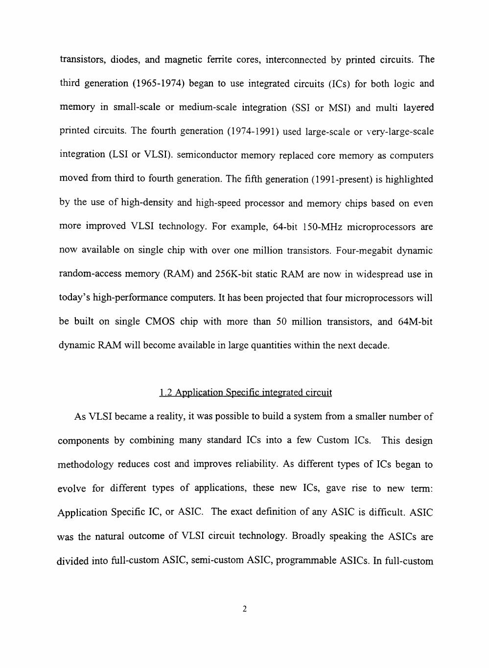
2.3.2.6 Condition Codes Register
The condition codes register (CCR) is an active-low edge tnggered four-bit latch
that is used to store the arithmetic and logical status flags generated b> the flags. Figure
2.12 shows the block diagram for the condition codes register. The circuit includes a
multiplexer, which allows any one of the four bits to be selected for output. In addition,
each logical status of each bit is available for output, providing for the selection of one of
eight possible combinations.
The CCR is loaded with the status flags from the Flag register on high to low
transition on pipeline register bit "CCRL". However, the control line is gated using OR
logic with the system clock. The result is to delay the drop of the control line until the
middle of the clock cycle. This provides enough delay so that the flags can be loaded in
the same clock cycle in which they are generated. This same principle is used in loading
the accumulator and index register.
From Instruction Register
CLOC Ccri
• To PC-Load
Figure: 2.12 CCR
24
2.3.3 Program Control Unit
The program control unit provides access to the extemal memon. unit for reading
of the program information and for reading and writing of data information. It consists of
the program counter, stack pointer, address bus buffer, data bus buffer and IDB
multiplexer.
The complete description of this unit is provided in the next chapter.
25

CHAPTER III
THE PROGRAM CONTROL L^TT
The program control unit provides access to the extemal memor\ unit for reading
of the program information and for reading and writing of data information. It consists of
the program counter , stack pointer , address bus buffer , data bus buffer and IDB
multiplexer.
Figure 3.1
3.1 The Extemal Memory unit
The extemal memory unit is not actually the part of the processor. The memory
data register (MDR) and memory address register (MAR) identifies it. Without extemal
memory, the processor has no information to process. Stored in the extemal memory are
the machine language instmctions that will be executed by the processor. The extemal
memory is also used to store data items to be processed. In addition, a segment of the
memory is reserved for the storage of the subroutine addresses. This segment in the
system is referred as the system "stack" and will be at the top of the memory segment, at
its higher addresses [5].
The read/write line defines whether memory is on a READ c\cle or a WRITE
cycle. On a READ cycle , the memory looks up data stored at the address identified on
the extemal address bus , placing it in the MDR. On WRITE cycle, the memory stores the
data presented to the MDR at the address of the extemal address bus. The Valid memor\
26

address (VMA) line must be a logical 1 to enable the memory to execute a READ or
WRITE cycle. The memory address register (MAR) is used to terminate the extemal
address bus. Its contents are always the same as the data currently on the extemal address
bus. The memory data register (MDR) is used to terminate the extemal data bus. On
READ operations, its contents are defined as the contents of the addressed memor>'
location. When there is valid and stable address on the extemal address bus, the
read/write line is logical 1, and VMA is tme, the memory enters its READ cycle. After a
propagation delay period, the contents of MDR are valid and ready to be copied into the
processor data bus buffer. Although the MAR and MDR appear to be sequential devices,
the memory unit is actually a combinational logic circuit. Its operation is a fiinction of its
stimulus and reaches a stable state when the stimulus is held stable. The final state occurs
after a propagation delay time referred as the access time of the device. It is necessary for
the stimulus to the memory unit to be stable for atleast access time before it reaches a
stable state. On read/write operations, it is necessary that the information on the extemal
address bus be stable while read/write line is a logical-1 and the VMA is tme.
3.2 The Data Bus Buffer
The data bus buffer utilizes an eight-bit low edge triggered latch to hold information
being read from and written to memory. An octal 2-1 multiplexer provides the inputs to
the DBB, which can be selected from either the memory unit. The output of the data bus
buffer drives port 0 of the IDB multiplexer and the bi-directional bus buffer is also a
ftmction of read/vvrite line, and is consistent with the READ/WRITE cycle operations.
27

3.2.1 Memory READ Data Direction
The read/write line is set to logical 1. This has following affects:
• It switches the bi-directional bus buffer to pass data from memor\' to the multiplexer.
• It switches the multiplexer to pass data from the bi-directional bus buffer to the DBB.
• It sets the memory unit to the READ mode.
• The DBB LOAD line will be dropped low, causing the DBB to be loaded \Mth
memory data immediately following a memory READ cycle.
3.2.2 Memory WRITE Data Direction
The read/write line is set to logical 0. This has the following effects:
• It switches the bi-directional bus buffer to pass data from the DBB to the extemal
memory unit.
• It switches the multiplexer to pass data from the intemal data bus (IDB) to the DBB
• It sets the memory unit to the WRITE mode.
• The data to be stored in the memory must be latched into the DBB during the READ
cycle.
3.3 The intemal data bus and IDB multiplexer
One of the primary paths for the data movement within the processor is the
intemal data bus. The IDB multiplexer selects any one of the following sources for the
placement on IDB:
• Data bus buffer (DBB),
28
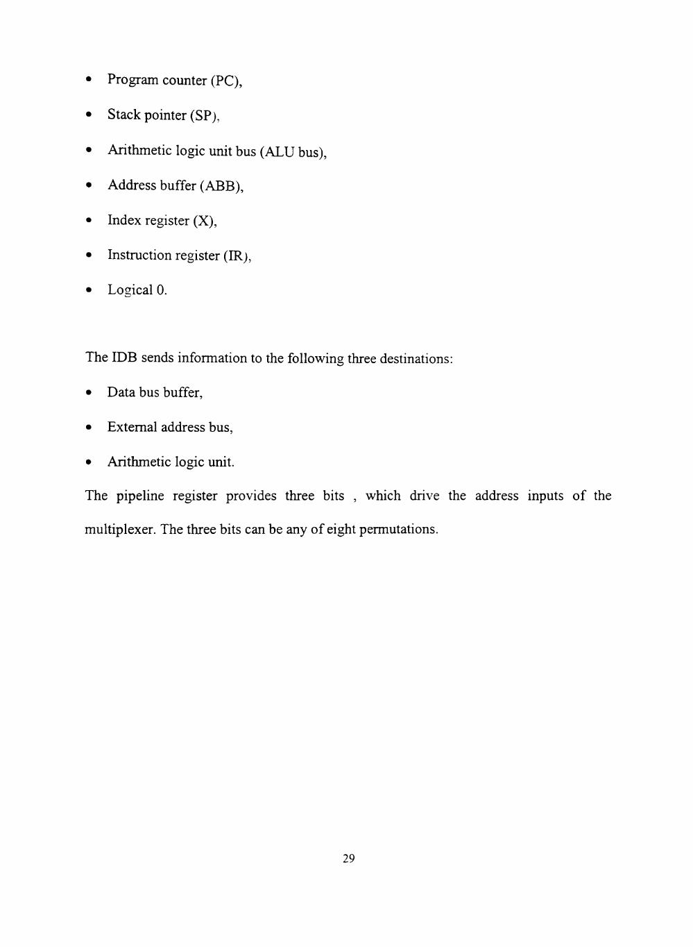
Program counter (PC),
Stack pointer (SP),
Arithmetic logic unit bus (ALU bus).
Address buffer (ABB),
Index register (X),
Instmction register (IR),
Logical 0.
The IDB sends information to the following three destinations:
• Data bus buffer,
• Extemal address bus,
• Arithmetic logic unit.
The pipeline register provides three bits , which drive the address inputs of the
multiplexer. The three bits can be any of eight permutations.
29
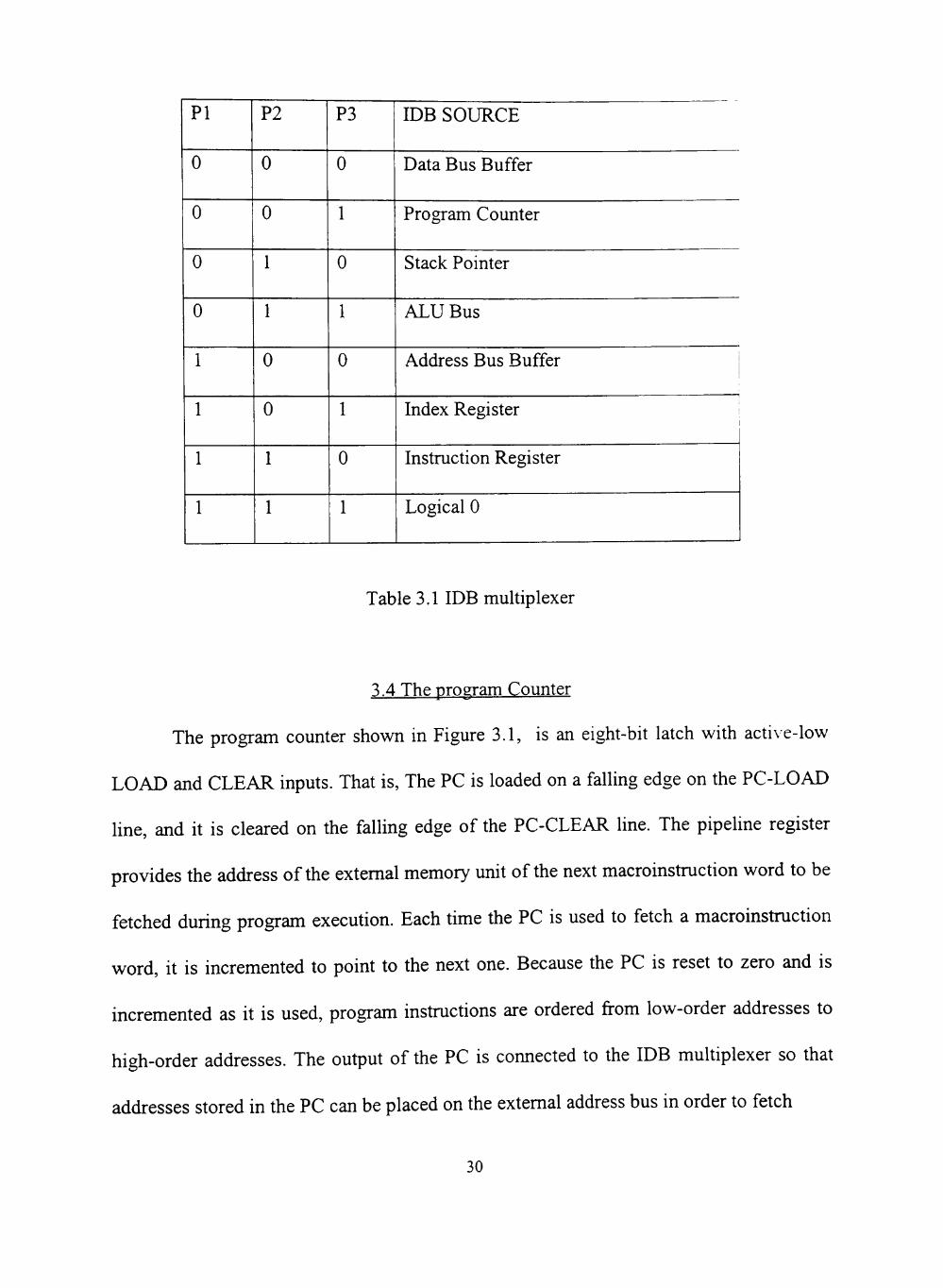
PI
0
0
0
0
1
1
1
1
P2
0
0
1
1
0
0
1
1
P3
0
1
0
1
0
1
0
1
IDB SOURCE
Data Bus Buffer
Program Counter
Stack Pointer
ALU Bus
Address Bus Buffer
Index Register
Instmction Register
Logical 0
Table 3.1 IDB multiplexer
3.4 The program Counter
The program counter shown in Figure 3.1, is an eight-bit latch with active-low
LOAD and CLEAR inputs. That is. The PC is loaded on a falling edge on the PC-LOAD
line, and it is cleared on the falling edge of the PC-CLEAR line. The pipeline register
provides the address of the extemal memory unit of the next macroinstmction word to be
fetched during program execution. Each time the PC is used to fetch a macroinstmction
word, it is incremented to point to the next one. Because the PC is reset to zero and is
incremented as it is used, program instmctions are ordered from low-order addresses to
high-order addresses. The output of the PC is connected to the IDB multiplexer so that
addresses stored in the PC can be placed on the extemal address bus in order to fetch
30

PC — /LOi-Ii — D7 Q7 — m Q6 — — DS Q5 —
D4 Q4 — DJ QJ — Di Qt — Dl 01 DO QO — / C L E
Figure 3.1 PC
microprogram instmctions. To increment PC, its contents are placed on the IDB b>
selecting portl on the IDB multiplexer. With PC contents on the IDB, the PC can be
incremented b\- the ALU and the loaded back into the PC from the ALU bus.
3.5 The Stack Pointer
The stack pointer shown in Figure 3.2, is an eight-bit latch with acti\ e-low LOAD
and CLEAR inputs. That is the SP is loaded on the falling edge of the SP_LO.\D line,
and it is cleared on the falling edge of the SP-CLEAR line. The purpose of the stack
pointer is to maintain the extemal memory address at the top of the system stack. It is
initialized to a logical 0 when the processor is reset. The system stack is a segment of the
extemal memory where temporary data can be stored by using stack pointer. The basic
idea is that stack pointer contains the address of the last item to b stored in the system
stack in memory.
To push an item onto the stack .the stack pointer is first decremented to point to the new
top of the stack , and then address in the stack pointer is used to store the item to be
pushed. This is referred to as a "pre-decrement PUSH"". To pop an item off the stack, the
address stored within the stack pointer is used to read the item from the memor\-. Once
the item has been read, the stack pointer is incremented to point to new top of the stack.
31

Since there is no command signal for incrementing or decrementing the stack pointer, the
contents of the SP must be placed on the IDB. With SP contents on the IDB. the SP can
be incremented or decremented by the ALU, then loaded back into the SP from the ALU
bus.
—
— — —
F
SP /LC&D D7 Q7 Hi Q6 D5 Q5 D4 Q4 D2 QJ Li QZ Dl 01 DO QO /CLR
igure 3.2 SP
3.6 The Address Bus Buffer
The address bus buffer shown in Figure 3.3, is an eight-bit latch with an active-
low LOAD input. That is, the ABB is loaded on the falling edge of the ABB-LOAD line.
The pipeline register provides the load control of the register. The purpose of the address
bus buffer is to provide a resource local to the microprogrammer for the storage of
temporary eight-bit data during the execution of a microprogram. For example, it is
common for the addresses to be calculated prior to use. The ABB can be used to hold
these calculated values and then to read from or write to memory at the calculated
address. The ABB is not accessible to the macroprogrammer. It is used only as needed in
the execution of a microprogram that is executing a single microinstmction.
Consequently the contents of the ABB are never maintained between two
macroinstmctions.
32

ABE - /LOAD - D7 - D6 - D5 - D4 - D2 - Di - D l - DO
Figure
07 Q6 05 04 QJ Qt 01 QO
'3.3 ABB
3.7 Program Control Unit Upgrades
The above method placed the program control unit and stack pointer ben\ een
ALU ftmction generator and the IDB multiplexer. This method was easy to program but
took two clock cycles for incrementing or decrementing. The draw back of this abo\e
method is use of ALU function generator for increment and decrement functions. The
ALU will provide significant number of arithmetic and logical fimctions, using it for PC
and SP management is a bit of overkill. Also, the incrementing and decrementing of the
PC and SP usually require extra clock cycles to execute, because ALU cannot be used for
any other purpose while incrementing and decrementing is taking place.
The solution to this dilemma is to provide an adder/subtractor circuit that is
dedicated to use by the PC and SP. With such design, the incrementing or decrementing
of the registers can be executed concurrently with other process. By organizing the
program control unit as a separate section of the design and driving it with the pipeline
register, we are enabling its operation to be concurrent with other processes, speeding up
the throughput of the system significantly.
33

The program control unit we are going to investigate also includes a P-word
macroinstmction stack, which is useful for storing remm addresses during subroutine and
ftmction calls. This implies that subroutines can be nested as deep as 17 levels and still
use the on chip stack, making memory access for stack operations unnecessary. This also
speeds up the throughput of the significantly. One drawback of this design is that there
are some apphcations in which subroutine nesting gets deeper than 17 levels. When these
algorithms are executed, a processor register must be used as a user stack pointer to
define a stack in extemal memory.
The PCU shown in Figure 3.4 , is a stand alone device that has only one data
input, one data output, six control bits and an input from the conditions code register. The
circuit is placed between the intemal data bus and extemal address bus.
34

•:U^
^
^ ^
Fig 3.4 PCU
35

CHAPTER IV
MICROPROGRAM INSTRUCTION FORMATS
As the block diagram is already realized ftmctionally, this chapter deals w ith the
hardware realization of each block. The following section is dedicated to explaining the
different types of addressing modes and instmctions associated with this program control
unit.
4.1 Addressing Modes
The method used to obtain address in memory where data processing is to take
place is referred to as an addressing mode. The effective address is that memory address
where data processing is to take place. Often the effective address is implied in the
instmction. Other times it is contained in the operand. Sometimes it must be calculated on
the basis of values of operands or processor register. The following are addressing modes
currently included in our discussion.
1. Implied Addressing. In implied addressing, the opcode contains all of the
information needed to execute the instmction. There is no operand and no necessity to
access memory during the EXECUTE cycle. Implied addressing is sometimes referred to
as inherent addressing.
2. Quick Immediate Addressing. This mode of addressing is used to initialize or
apply constants to intemal processor register when the value of the constant can be
expressed in three binary bits. These bits are stored in the three least significant bits of
36

the instmction register and fetched during the FETCH cycle. The contents of the IR are
placed on the IDB in order to felicitate the completion of the instmction.
3. Immediate Addressing. This mode is used to initialize or apply constants to
intemal processor registers when the value of the constant can be expressed in four to
eight binary bits. The operands follows the opcode in the program and must be fetched
into the DBB during the EXECUTE cycle. The contents of the DBB are placed on the
IDB in order to facilitate the completion of the instmction. The effective address is
literally the program counter, because it points to the operand.
4. Direct Addressing. In this mode, the operand of the instmction contains the
effective address. During the EXECUTE cycle, the operand must be loaded into the DBB
and then must be placed on the IDB, where it is used to access the memory location to be
processed. Direct addressing is also referred to as an absolute addressing.
5. Direct Index Addressing. In direct indexed addressing, the operand of the
instmction is added to the contents of the index register in order to determine the
effective address. In a typical application, the operand is used as a base address of a table
of data, and the index register is used as a displacement that can be moved up and down
the table. During the EXECUTE cycle, the operand must be fetched into the DBB and
passed through the ALU with the index register added to it. It then must be placed in the
address bus buffer. The contents of the ABB are then placed on the IDB in order to
facilitate the completion of the instmction. Direct indexed addressing is also referred to
as absolute indexed addressing.
37

6. Indirect Addressing. In this addressing mode, the operand of the instmction
points to a memory location containing the effective address. When direct addressing is
used, the effective address is the operand, and is therefore a constant. Indirect addressing
allows the effective address to be a variable by locating it in memory in a data area
separated from the macroprogram. During the EXECUTE cycle, the program counter is
used in a READ cycle to fetch the operand into the DBB. The DBB is then used in a
READ cycle to fetch the effective address into itself Now with the effective address in
the DBB, the DBB is placed on the IDB in order to facilitate the completion of
instmction.
7. Relative Addressing. In relative addressing, the operand of the instmction is
added to the contents of the program counter in order to determine the effective address.
When relative addressing is used, the program operation is not affected by \'ar\ang the
beginning address in memory where the program is stored. As the program is relocated to
a different address, the program branches and data references move along with it.
4.2 Instmction Set of PCU
The instmctions are divided into two sets. The first set of instmctions, with
opcodes of 00000 through 01111, are unconditional. Their operation is unaffected by the
CC input.
38

4.2.1 Unconditional PCU instmctions
00000 PRST (Reset)
This instmction might be included in the power-up initialization program. It clears
program counter, stack pointer and places a logical 0 on the outputs of the PCU.
00001 FPC (Fetch PC)
This is most commonly used command. The current contents of the program
counter are presented at the output of the PCU, enabling fetch from the memor>' using
program counter. Halfway through the clock cycle, the PC can be incremented by setting
CI=1.
00010 FR (Fetch R)
This instmction places the R register on the outputs of the PCU. Halfway through
the clock cycle. The PC can be incremented by setting CI=1. The R register is a scratch
pad register local to the microprogrammer for any purpose. Its contents are never defined
upon entry to a microprogram. It is not used to pass information between microprograms.
00011 FD (Fetch D)
This instmction places the input of the PCU on its outputs. Because the PCU
inputs are tied to the intemal data bus. This instmction has the effect of setting up a data
path between the IDB and the MAR. This allows us to generate an address within any
resource that can be placed on the IDB. Halfway through the clock cycle. The PC can be
incremented by setting CI=1.
39

00100 FRD (Fetch R+D)
This instmction places the sum of the R register and the data on the IDB on the
output of the PCU. This allows for realtive and index addressing using the two soources
as operands. The contents of the R register are not affected. Half\va\' through the clock
cycle, the PC can be incremented by setting CI=1.
00101 FPD (Fetch PC+D)
Intended for relative addressing, this instmction adds the value on the D inputs to
the contents of the program counter and places the sum on the PCU output. Halftvay
through the clock cycle, the PC can be incremented by setting CI=1
00110 FPR (Fetch PC+R)
Intended for relative addressing, this instmction adds the contents of the R
register to the contents of the program counter and places the sum on the PCU output.
Halfway through the clock cycle, the PC can be incremented by setting CI=1
001IIFSD (Fetch S+D)
Intended for indexed addressing, this instmction adds the current \'alue on the D
inputs to the value last placed on the top of stack and places the sum on the pcu output.
.Halfway through the clock cycle, the PC can be incremented by setting CI=1
01000 FPLR (Fetch PC to Load R)
This instmction is used to load the R register with the current contents of the
program counter. Note that load of the register takes place on the rising edge of the clock
pulse. Halfway through the clock cycle, the PC can be incremented by setting CI=1
40

01001 FRDR (Fetch R + D to Load R)
This instmction places the sum of the R register and the current \alue on the D
inputs on the outputs of the PCU. It also loads the sum into the R register on the rising
edge of the clock. The effect is to add the current value of the D inputs to the R register. .
Halfway through the clock cycle, the PC can be incremented by setting CI=1
01010 PLDR (Load R)
This instmction places the current value of the program counter on the PCU
outputs and loads the R register with the current value on the D inputs on the rising edge
of the clock.
Halfway through the clock cycle, the PC can be incremented by setting CI=1
0101IPSHP (Push PC)
This instmction places the current value of the program counter on the PCU
outputs and pushes it onto the top of the stack. The stack pointer is updated in the
process. Halfway through the clock cycle, the PC can be incremented by setting CI=1.
OllOOPSHD(PushD)
This instmcion places the current value of the program counter on the PCU
outputs and pushes the current value on the D inputs onto the system stacks. The stack
pointer is updated in the process. Halfway through the clock cycle, the PC can be
incremented by setting CI=1.
01101 POPS (Pop S)
This insttmction places the current value on the top of the stack on the PCU
outputs and decrements the stack pointer by 1 . The result is effecti\ely a "pop address"
41

operation; that is, the address on the top of the stack is popped off and placed on the
outputs of the PCU for subsequent memory cycle. Halfway through the clock cycle, the
PC can be incremented by setting CI=1.
OlllOPOPP(PopPC)
This instmction places the current value of the program counter on the PCU
outputs. Halfway through the clock cycle, the PC can be incremented by setting CI=1.
Also, the stack pointer is decremented, effecting a "pop"" operation. How e\ er. there is no
transfer of stack data.
01111 PHLD (Hold)
This instmction is an unconditional hold, or "no operation"', command. The
current contents of the program counter are placed on the outputs of the PCU.The current
contents of the PC,R and stack are not affected.
4.2.2 Conditional PCU instmctions
Fail condition: cc=l Execute FPC
When the output of the CCR(status registers) is enabled, the state of the CCR
output determines whether or not a conditional PCU command is executed. When CC=1.
the fail condition exists. In this event, the current contents of the program counter are
placed on the PCU outputs. Halfway through the clock cycle, the PC can be incremented
by setting CI=1. This condition is same as the unconditional FPC command.
Pass Condition: CC=0
42

10000 JMPR (Conditional Jump R)
This instmction loads the program counter with the current contents of the R
register plus the value of the CI flag. This results in a program jump to R-rCI. If the
output of the CCR is enabled, the instmction is conditional.
10001 JMPD (Conditional Jump D)
This instmction loads the program counter with the current \ alue on the D inputs
to the PCU plus the current value of the CI flag. This results in a program jump to D-CI.
If the output of the CCR is enabled. The instmction is conditional.
10010 JMPZ (Conditional Jump Zero)
This instuction loads the program counter with $0+CI. This results in a program
jump to address O+CI. If the output of the CCR is enabled. The instmction is conditional.
10011 JPRD (Conditional Jump R+D)
This instmction loads the program counter with the sum of the current contents of
the R register and the current value of the D inputs to the PCU. The result is a program
jump to R+D+CI. If the output of the CCR is enabled, the instmction is conditional.
10100 JPPD (Conditional Jump PC + D)
Intended to implement relative addressing, this instmction adds the value
currently on the D input to the program counter. This results in a relati\ e jump. The jump
is relative to the program counter, and the displacement of the jump is found at the D
input to the PCU. If the output of the CCR is enabled, the instmction is conditional.
10101 JPPR (Conditional Jump PC + R)
43

Intended to implement the relative addressing, this instmction adds the current
value of the R register to the program counter. This results in a relative jump. The jump is
relative to the program counter, and the displacement of the jump is found in the R
register. If the output of the CCR is enabled, the instmction is conditional.
10110 JSBR (Conditional Jump Subroutine R)
This instmction pushes the current value of the program counter onto the stack
and then loads the current contents of the R register plus the value of the CI flag into the
program counter. The result is a jump to R+CI after pushing the PC. If the output of the
CCR is enabled, the instmction is conditional.
10111 JSBD (Conditional Jump Subroutine D)
This instmction pushes the current value of the program counter onto the stack
and then loads the value on the D input plus the value of the CI flag into the program
counter. The result is a jump to D + CI after pushing the PC. If the output of the CCR is
enabled, the instmction is conditional.
11000 JSBZ (Conditional Jump Subroutine Zero)
This instmction pushes the current value of the program counter onto the stack
and the loads the program coounter onto the stack and then loads the program counter
with zero plus the CI flag. The result is jump to $0 + CI after pushing the PC. If the
output of the CCR is enabled, the instmction is conditional.
11001 JSRD (Conditional Jump Subroutine R + D)
This instmction pushes the current value of the program counter onto the stack
and then loads the sum of the contents of the R register and the value on the D input plus
44

the value of the CI flag into the program counter. The result is a jump to R + D + CI after
pushing the PC. If the output of the CCR is enabled, the instmction is conditional.
11010 JSPD (Conditional Jump Subroutine PC + D)
Intended to implement a relative subroutine jump, this instmction pushes the
current value of the program counter onto the system stack. It then adds the \ alue
currently on the D input to the program counter. This results in a relative jump after
pushing the PC. The jump is relative to the program counter, and the displacement of the
jump is found at the D input to the PCU. If the output of the CCR is enabled, the
instmction is conditional.
11011 JSPR (Conditional Jump Subroutine PC + R)
Intended to implement a relative subroutine jump, this instmction pushes the
current value of the program counter onto the system stack. It then adds the value
currently on the R register to the program counter. This results in a relative jump after
pushing the PC. The jump is relative to the program counter, and the displacement of the
jump is found in the R register of the PCU. If the output of the CCR is enabled, the
instmction is conditional.
11100 RTS (Conditional Return from subroutine S)
This instmction is intended to execute a retum from subroutine w here the retum
address is stored on the top of the system stack.The top of the stack is popped into the PC
, and the stack pointer is decremented, pointing to the last item stored on the stack. If the
output of the CCR is enabled, the instmction is conditional.
11101 RTSD (Conditional Retum from Subroutine S - D)
45

This instmction is intended to execute a retum from subroutine w here the retum
address is calculated by adding the current value of the D input to the value stored on the
top of the system stack.The top of the stack is popped into the PC, the value of the D
inputs is added to it and the stack pointer is decremented, pointing to the last item stored
on the stack. If the output of the CCR is enabled, the instmction is conditional.
11110 CHLD (Conditional Hold)
This instmction is a conditional hold, or "no operation" command. The current
contents of the program counter are placed on the outputs of the PCU. The current
contents of the PC, R and stack are not affected. If the output of the CCR is enabled, the
instmction is conditional.
11111 PSUS (Conditional PCU Suspend)
This instmction is designed to place the PCU in a suspended mode of operation
when not in use. It places the outputs of the PCU into a high-impedance state and has no
affect on the PC, R register, SP or system stack. If the output of the CCR is enabled, the
instmction is conditional.
4.3 Hardware realization of Program Control Unit
The Program control unit consists of the stack, stack pointer, ALU, ALU operand
selector, the program counter, the R register (scratch pad register) and five different
multiplexers.
46

4.4 Arithmetic Lo^ic I Init
JT
I I
FA Fft c i n . 0 couc I
FA It
eowc
!i y
FA
eout
FA
tout
FA FA FA I t
- ^ ^ ^ = f ^ ^ -a
Figure 4.1_ALU
This is a eight-bit adder shown in Figure 4.1, whose operands are provided b\ the
ALU operand selector. The output of the adder is on extemal bus which is provided to
extemal memory unit and also program counter, which increments and points to the next
address location. The hardware realization of full adder is as shown in Figure 4.2.
0 K ^ - c> >1
^]:>^-
> ^s>-
K>-
Figure 4.2 Adder
Where sum = A (exor) B (exor) Cin
G= A (exor) B
Carry out= A*B+ G* Cin
4.5 Arthimetic Logic Unit operand selector
The operand selector shown in Figure 4.3, provides operands to Adder depending
on the control inputs /CC, A0,A1. /CC control is provided by status shift control unit.
47

When the output of the CCR is enabled, the state of the CCR output determines w hether
or not a conditional PCU command is executed. When CC= 1 fail condition exists. In
this event, the current contents of the program counter are placed on the PCU outputs.
The tmth table for the control logic of the ALU operand selector is:
Table 4.1 ALU operand selector
/CC 0 0 0 0 1 1 1 1
AO 0 0 1 1 0 0 1 1
Al 0 1 0 1 0 1 0 1
Function Pass A PassB
Pass A, B Reset
Pass A Pass A Pass A Pass A
4S

C y_y V
V
• • Z > — '
- z^-^
,: 2> .
E- —
. E> .-_
E —
E) .-
. • E > •
;C
E^
E r -f-'
E>-
>E>-
E ^
E>-
=[I>
=C-
-O-
- c-
;-0
-=c--:=C -=c-
Figure 4.3. ALU operand selector
49

4.6 Stack Pointer
The stack pointer is supposed to take in a two bit input and produce a 3 bit
address and a stack fiill bit as an output. The 2 bit input (SI and SO) and their
correspondence to the operation of the stack pointer are shown in the Table 4.2. below.
For a block diagram of the stack pointer please, refer to the Figure 4.4 below.
Table 4.2 Instmctions
SI
0
0
1
1
so
0
1
0
1
Instmction mapping
i
Clear
Hold
i
Push
Pop
i
! M xnc
d e c
«: J 3
Ml. \ i i ^
:0-
c 4-bitinux
-5r\
4-l)itjimx JTL
4bitreg , 0
I i r
/v
Figure 4.4 Stack pointer
4-bitiiiux
1 ^ i2
bO b l b ! b :
4t)itreg
50

As a convention for the stack pointer, it was decided to use speculative prediction
and have two pointers. One pointer points to the next push location (output of the positive
edge register) and the pop pointer (address flowing from the decrementor to the third
mux). This assures that the word lines will be valid once the SI and SO inputs comes
since the third mux can choose one of these address pointers.
It was also decided that a stack access should only take one clock cycle and
hence, the stack pointer had to supply a valid address on the high part of the clock and the
read or write operation to occur on the low part of the clock.
Clear. On a clear, the second mux (that is the one with S1 as a selector) chooses
the 4 bit input on the 0 selector side. This input is an AND of SO and the current pointer
which results in an output of 0 (since SO is 0), thus resetting the counter to zero on the
next clock edge. Note that clearing is an operation that does no memory accesses such
that it is not important what the pointer to the memory is at the time of a clear. The
pointer just needs to be set to zero on the next clock edge.
Hold. Similar to the clear, there is really no memory access on a hold and it
should just be assured that the address pointers do not change. This is assured by the third
second mux selecting the 0 input which for this case is just the current output of the
positive edge register AND'ed with S0=1.
Push. When a push instmction comes, the push pointer has to flow through to the
stack memory and be valid on the low part of the clock. This is done by the third mux
which lets the output of the positive register (push pointer) through. The presence of the
51

negative edge register at the end will be discussed later in the timing considerations.
Since a push is made, the pointers needs to be changed to point to the next memor>
location for the next push. This is done by
the combinational logic to the left of the positive edge register. Keeping in mind that
S1=0 and Sl=l, it can be easily seen that the incrementor output will pass through as the
input to the positive edge register which will be latched at the next clock edge.
Pop. On a pop instmction, the pop pointer should be let through to the stack
memory. This is done by the third mux through the negative edge register. And similar to
the push instmctions, the pointer will be updated by the combinational logic to the right
of the positive edge register.
4.7 Stack Memory
The stack memory is connected to the datapath, getting some of its inputs from
the PC register and input data bus. ft provides inputs to the multiplexer whose datapath is
given to ALU. It also takes in a 3-bit address input from the stack pointer [2].
It was implemented using an 8x12-bit SRAM memory module, a clock coupled decoder,
a write signal generator and a 12 bit negative edge register. A diagram showing the
interconnections is shown Figure 4.5.
52

5- 1^
C5
-: K -l
y ^ v ^ v ^ * ^ ^
t- . '» " 0 , J . CI" j^ ^J . CIl ,_ » M- -i_l
r
0| = = » " Q _ X
* — * I " * ' - ->'
» I _ . " l - J
k H'^' ^
H'?'"-J_
I i
i!4
1
» 1
! j * * "
1
> 1
—-
1
- 1
!
••" » 1
• I
- 1 —
-nl-
_L
I k I
-n-, i ' ' I i ' - 1 — -
xH -4^
i -^ 'li! • ' — 0 - . = ' " o | -
S I k
: L 4 -| J^ , i i . c m „ ' —
s au.J_-
i ^ ^ n ^ j ^ XLL l-Li^LV_L±
Figure 4.5 Stack Memory
53

The clock coupled decoder shown in Figure 4.6, assures that the word line is only valid
to the low edge of the clock cycle when the read and write opreation occurs.
® 1 ^1
• i-
I
*-
y
>
>
>
>
m
) K>"
J
I
~-\
J
y
\
^ ^ ' •
-E> " "
• ^
) E>"^
") E>'-
'^ K> "•""
-E>' ^ ^
Figure 4.6 Decoder
The 8- it register at the end is to assure that the write data will be \ alid until the write is
done.
54

4.8 PC and R register^;
The negative edge triggerred eight bit register is shown in Figure 4.". The
program counter(PC) holds the value which always points to the next address location in
memory. The R register is simply a scratch pad register which is pro\ided to hold the
values between cycles of an instmction. They are loaded by pipeline register bit.
-- E>-
Cllc ^ d "•
EOatcb e l k e l k
o o a t c n — e l k I — elk 1
a i • elk - — e l k
^
Figure 4.7 Register
The negative edge triggred Dlatch is implemented as shownin Figure 4.8.
• ^
^ E>
Figure 4.8 Dlatch
4.9 Muhiplexer
There are five 2 to 1 eight-bit multiplexeres which provide the datapath between
different modules in the design. The different combinations of the control signals of these
multiplexers form different set of instmctions. The multiplexer is shown in Figure 4.9.
5!)

V
:'-" E>- J- - ^
= 01 E > - J- - ^ - - -
.'.: K>- J- O ^ E>- ^
y i:>—^ -U4 E > -
- ^
SU5 E > -> -E>
:0f K>-> C> '-'"
507 E > -> o -K>
ii« K>->
i l l K > ->
- : K>->
K> >
ii4, E>- "^ ^
ii^ IK>->
iif K>->
17 E > -
Figure 4.9 MUX
56

CHAPTER V
LAYOUT OF 8-BIT PROGRAM CONTROL L^NIT
5.1 Introduction to layouts
There are several approaches that can be used to describe an integrated circuit
(IC). In the basic sense, an IC is an electronic network that has been fabricated on a
single piece of a semiconductor material such as silicon. The silicon surface is subjected
to various processing steps in which impurities and other material layers are added w ith
specific geometrical pattems. The steps are sequenced to form three-dimensional regions
that act as transistors for use in switching and amplification. Passive elements, such as
resistors and capacitors, are not always included as elements in the circuit, but anse as
parasitic elements due to the electrical properties of the materials. The w iring among the
devices is achieved using interconnects, which are pattemed la\ers of low-resistance
materials such as aluminum. The resulting stmcture is equivalent to creating a
conventional electronic circuit using discrete components and copper wires.
So we can define an integrated circuit as a set of pattemed layers. Each la\'er has
specific electrical characteristics, such as sheet resistance, and is pattemed according to
layers above and below. Stacking different material pattems results in geometrical objects
that function electrically as devices or interconnects.
A layout editor such as L-Edit is used to design the pattems on each layer and
accomplish the physical design of the chip. The drawings represent the patterning of each
layer, and the overall image can be interpreted as the top view of the chip. Each la\er is
57

distinguished by a separate color on the computer monitor so that three-dimensional
stmctures such as transistors can be distinguished.
5.2 Design Philosophies
Digital VLSI can be implemented at several levels depending upon the starting
point. The most common divisions are as follows:
• Full Custom.
In full custom design every detail of the integrated circuit layout needs to be
completed. At this level, all gates must be designed, drawn and simulated.
• Cell-based.
Cell-based designs are based on existing cells stored in a library, which is a
collection of pre-designed gates and modules. The properties of each cell such as speed
and layout dimensions are provided to the system designer, who provides the
arrangement and interconnect to implement the system. Application-specific integrated
circuits (ASICs) are usually constmcted in this manner.
• Gate arrays.
Gate arrays consist of arrays of MOSWest that can be wired using inter-connect
lines to implement the desired ftmctions. Logic circuits can be prototyped very quickly
using this approach.
CMOS standard cells were used to layout the 8-bit program control unit. CMOS is
recognized as a leading contender for existing and future VLSI systems. CMOS provides
an inherently low power static circuit technology that exhibits a lower power-dela\'
58
• ^
product than other comparable design-mle Amos or pomes technologies. It also pro\ides
high density, primarily because the transistors can be made \er\' small.
Standard cells are designed to fit together like bricks in a wall. Standard cell design
allows the automation of the process of assembling an ASIC. Groups of standard cells fit
horizontally together to form rows. The rows stack vertically to form rectangular blocks.
5.3 Cells and Hierarchy
In this design cell is the basic unit. At the logic level this may be a simple logic
function or a complex Boolean operation. The circuit equivalent of a cell is a defined
layout pattem with given dimensions, input output ports and specified electrical
performance. On the other hand cell may be defined as a set of HDL declarations or
timing diagrams. A system is constmcted by interconnecting cells together [6]. At the
chip design level the most important factors are
5.3.1 Area and dimensions
Every cell consumes chip area and has a particular geometrical shape associated
with it. Both are important for high-density integration.
5.3.2 Ports
The location of the input and output ports is very important for routing the data
path. Also the power supply and ground are usually needed to provide electrical energy to
the cell.
59
• c \

5.3.3 Interconnect strategy
The cells must be wired together using the interconnect layers. Even with three or
four separate conducting layers, this can be the limiting factor in the logic density.
Cell level 3 -V ./7
Cell level 1 4
I ; I
CcJl level I
(a) Prirttitives Only ih]\risLances
Figure 5.1: Cells and Hierarchy
ic) Nested Insiynces
5 4 The Floor Plan
The floorplan is a physical description of an ASIC.ft is a mapping between the
logical description and the physical descnption. The goals of floorplannmg are to:
• Arrange the blocks on a chip,
• Decide the location ofthe I/O pads,
• Decide the location and number of the power pads,
• Decide the type of power distribution, and
60

• Decide the location and type of clock distribution.
We need to control the aspect ratio of our floorplan because the chip have to fit
into the die cavity. Generally the interconnect channels have a certain channel capacity;
that is, they can handle only a fixed number of interconnects. One measure of congestion
is the difference between the number of interconnects the are actually need, called the
charmel density, and the channel capacity. During floorplanning step we assign the areas
between blocks that are to be used for interconnect. This process is known as channel
definition or channel allocation.
Every chip communicates with the outside world. Signals flow onto and off the
chip and we need to supply power. So I/O and power constraints are considered earh' in
the floorplarming process. Special power pads are used for the positi\'e supply, or VDD,
power buses and the ground or negative supply, VSS or GND. Usually one set of
VDD/VSS pads supplies one power ring that mns around the pad ring and supplies power
to the I/O pads only. Another set of VDD/VSS pads connects to a second power ring that
supplies the logic core. We sometimes call the I/O power dirty power since it has to
supply large transient currents to the output transistors. We keep dirty power to avoid
injecting noise into the intemal-logic power. I/O pads also contain special circuits to
protect against electrostatic discharge. The circmts can withstand very short high-voltage
pulses that can be generated during human or machine handling.
61
WMHTv^

5.5 Placement Goals and Objectives
The goals of the placement are to arrange all the logic cells w ithin the flexible
blocks on a chip [3]. Ideally, the objectives ofthe placement step are to
• Guarantee the router can complete the routing step
• Minimize all the critical net delays
• Make chip as dense as possible
• Minimize the power dissipation
• Minimize cross talk between signals
The limiting factor in high-density system design is the interconnect routing and
connections. One reason for the situation is the existence of basic layout mles such as:
The minimum width and spacing rules for wires on the same layer and
Surround design mles that are required for contacts and vias.
These automatically limit the density of the wiring. Since, each layer is
intrinsically two-dimensional, wires on the same layer cannot cross without creating an
electrical short-circuit. Interconnect routing is complicated by parasitic electrical
coupling among lines that are physically close to each other. This is termed "crosstalk",
and can cause data transmission errors. Both logic '0' and logic ' 1 ' voltage levels can be
effected due to crosstalk .
Crosstalk problems can be difficuh to isolate, particularly in high-density layouts.
It is therefore best to avoid in the original design. The effects can be minimized by
obeying all design mle spacing, avoiding long lengths of parallel lines and purposeh
introducing "kinks" into the lines to disturb the coupling.
62
* ^
5.6 Routing
Once the designer has floor planned a chip and the logic cells withm the flexible
blocks have been placed, it is time to make connections by routing the chip. Routing is
usually split into global routing followed by detailed routing [3].
5.6.1. Global routing
The input to the global router is a floorplan that includes the locations of all the
fixed and flexible blocks; the placement information for flexible blocks; and the locations
of all the logic cells. The goal of global routing is to provide complete instmctions to
detailed router on where to route every net. The objectives of global routing are one or
more ofthe following:
• Minimize he total interconnect length.
• Maximize the probability that the detailed router can complete the routing.
• Maximize the critical path delay.
In both floorplanning and placement, with minimum interconnect length as an
objective, it is necessary to find the shortest total path length connecting a set of
terminals. This path is the MRST, which is hard to find. The altemative, for both
floorplanning and placement, is to use simple approximation to the length ofthe MRST.
5.6.2 Detailed Routing
The goal of detailed routing is to complete all the connection between logic cells.
The most common objective is to minimize one or more ofthe following:
63
^

• The total interconnect length and area
• The number of layers changes that the connections have to make
• The delay ofthe critical paths
Minimizing the number of layer changes corresponds to minimizing the number
of vias that add parasitic resistance and capacitance to a connection.
The global routing step determines the charmels to be used for each interconnect.
Using this information the detailed router decides the exact location and layers for each
interconnects. These mles determine the metal 1 routing pitch. WE can set the metal 1
pitch to one of three values:
1. Via-to-Via (VTV) pitch.
2. Via-to-line (VTL) pitch, or
3. Line-to Line (LTL) pitches.
In two level metal CMOS ASIC technology we complete the wiring using the two
different metal layers for the horizontal and vertical directions, one layer for each
direction. This is Manhattan routing.
After detailed routing is complete two different checks are performed before
fabrication. The first check is Design-Rule check (DRC) to ensure nothing has gone
wrong in the process of assembling the logic cells and routing. The DRC may be
performed at two levels. Since the detailed router normally works with logic cell
phantoms, the first level of DRC is a phantom-level DRC, which checks for shorts,
spacing violations, or other design mle problems between logic cells. The other check is a
64

layout versus schematic check to ensure that what is about to be committed to sil icon IS
what is really wanted. The floorplan is shown m Figure 5.2.
VDD
GNT)
CLOCK
Fig 5.2 Floorplan
65
• X
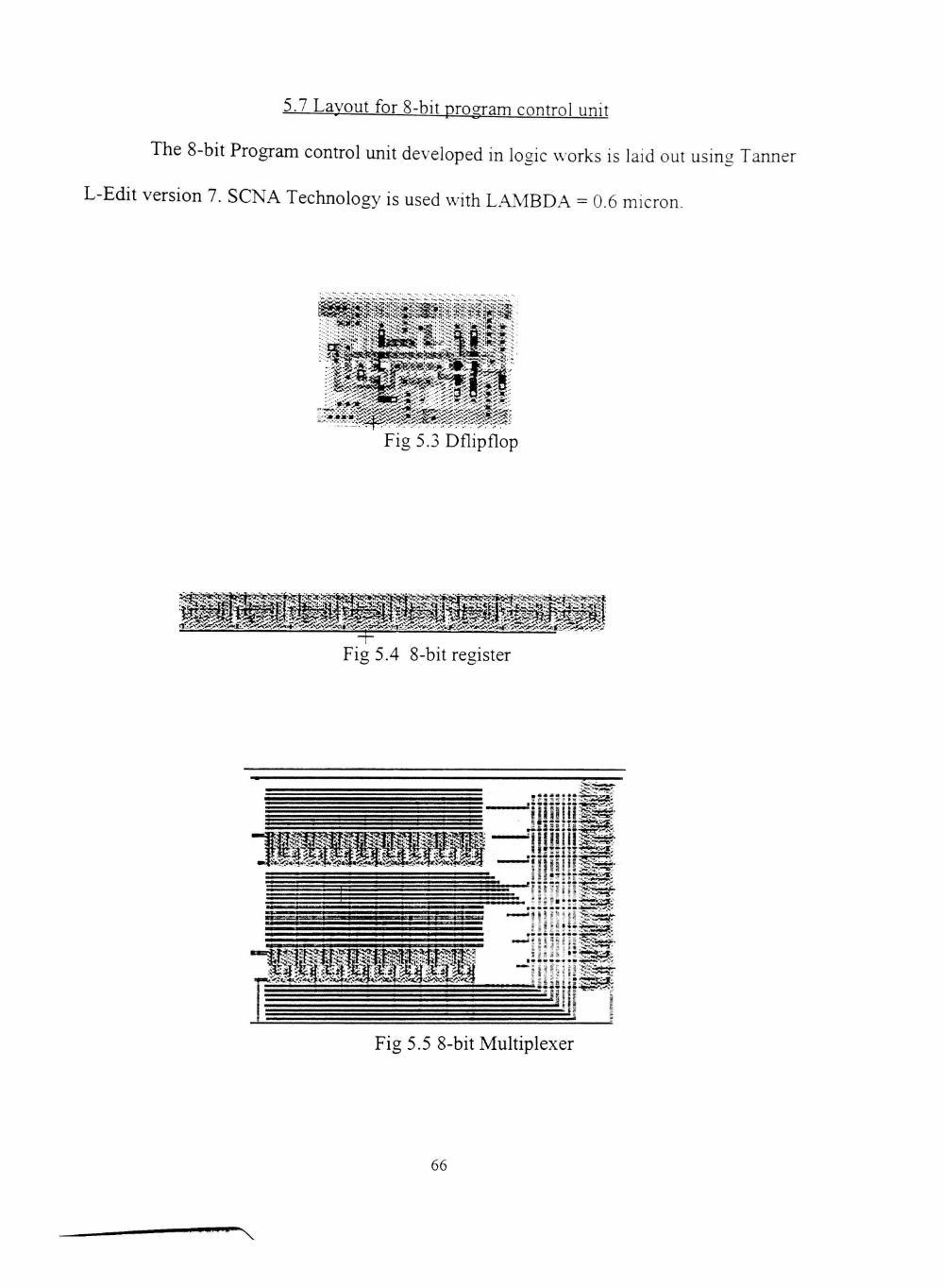
5.7 Lavout for ? -hit program control unit
The 8-bit Program control unit developed in logic works is laid out using Tanner
L-Edit version 7. SCNA Technology is used with L.AMBDA = 0.6 micron.
Fig5.3Dflipflop
Fig 5.4 8-bit register
Fig 5.5 8-bit Multiplexer
66

+
Fig 5.6 8-bit adder
Fig 5.7 8-bit ALU operand selector
I aES3> ^
msmsM n
Fig 5.8 8-bit decoder
67

CHAPTER VI
RESULTS
An 8-bit "MODULAR PROGRAM CONTROL UNIT"' was successfulK
implemented using a cell based implementation technique in Logic Works 3.0.3. The
physical layout was laid out in L-Edit (SCNA Technology is used with LAMBDA = 0.6
micron) and extracted into Pspice. Successful simulations were mn on extracted files in
Pspice.
The hierarchical stmcture of the design is exploited to test the design at different
levels. First, individual modules are tested at the gate level with Logic works and Pspice.
Since the interfaces between the different modules are well defined, it is rather
straightforward to generate test cases to check if input/output constraints are satisfied.
Next, when it was found that individual components were working correctly, all the
schematics are combined into a schematic version of the program control unit. Once the
gate-level simulations were found to be successful, the individual cells were laid out,
simulated and tested.
68
'N

6.1 Gate-level Component Testing: (All w^aveforms need to labeled as figures)
Stack pointer:
S0=0,S1=1 CLEAR
S0=1.S1=0 HOLD
so si elk ¥0
Wl IJ2
2. r
S0=0,S1=1 PUSH
S0=1,S1=1 POP
fi
elk
wl
u2
t cli
;2
Fig 6.1 Stack pointer results
In Figure 6.1, SO and SI are the control lines for the stack pointer. At the falling edge of
the clock, when S0=0, S1=0 then wO=0, wl=0 and w2=0. That means that stack pointer
is cleared to address location 000. When S0=1, S1=0 the stack pointer holds the current
value of address. From the Figure 6.2, when SO and SI change to 1 and 0, then the value
at wOwl w2 remain at Oil. When S0=0,S1=1 the value is pushed on the stack by
incrementing the address. As can be seen from the figure 6.3, when S0=0,S1==1 the value
w2, wl, wO is 110.
69

After each falling edge of the clock the \alue is incremented to
111,000,001,010.... and so on. During the pop command the value is read from the stack
by decrementing the address. From the figure 6.4, S0=1 and Sl = l. [w2 wl wO] =11 l.At
each falling edge ofthe clock the value at [w2 wl wO] is decrements by one.
Program Counter and R-relister:
dO dl d2 d3 d4 d5 d6 d7 en qO
ql q2 q3 q4 q5 q6 q7
Fig 6.2 PC and R results
The program counter and R- register are 8-bit latches, as shown in Figure 4.7 and
Figure 5.4. The values ofthe data inputs are latched at the falling edge ofthe clock. Any
further changes in input after the falling edge are not noticed till the falling edge of the
clock. In Figure 6.5, d0...d7 are data inputs and q0...q7 are corresponding outputs and
'en', is the enable input ofthe register. Consider any falling edge ofthe enable. The data
70
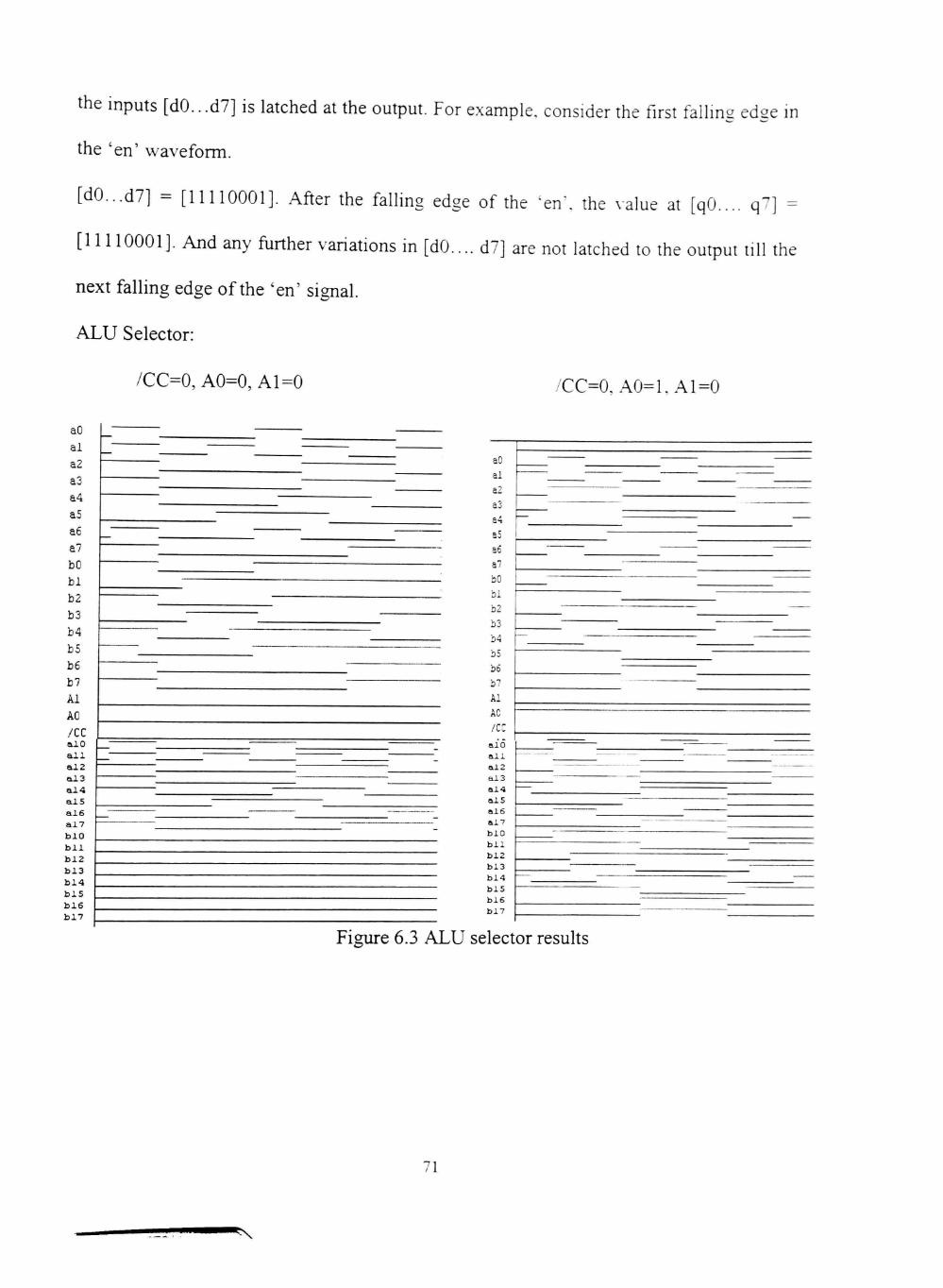
the inputs [d0...d7] is latched at the output. For example, consider the first falling edge in
the 'en' waveform.
[d0...d7] = [11110001]. After the falling edge ofthe 'en-, the value at [qO.... q7] =
[11110001 J. And any ftirther vanations m [dO.... d7] are not latched to the output till the
next falling edge ofthe 'en' signal.
ALU Selector:
/CC=0,AO=0, A1=0 /CC=0. A0=1.A1=0
aO
a l
a2
a3 a4
a5
a6
a7
bO b l
b2
b3
b4 bS
b6
b7 Al
AO
/CC a l O
a l l
&1Z
a l 3
a l 4 a l S
a l 6 a l 7
b l O
b l l
b l 2
b l 3
b l 4
b i s
b l 7
—
tt2
^^.
— a4
ai
a6 • - a /
' bO
hi
b2
b3 , 34
b5 b6
Dl
Al AC
/c: a l U
a l l
a l 2
Hi 3 ttl4 a l S
- • a l 6 a i 7 b l O
b l l
b l 2
b i 3
- • • • • b i 4
b i b
b l 6
'• '• b l 7
—
- - • —
•
Figure 6.3 ALU selector results
71
mm ^

The ALU selector as shown in Figure 4.3 and Figure 5 J. selects the operands
based on the combination of/CC, AO, Al. In Figure, A inputs are from AO.. .A7. B inputs
are from B0...B7. The controls are /CC, AO, Al. The outputs are AlO.... A17. BIO....
B17. As can be seen in Figure 6.6, when /CC=0 A0=0, A 1=0, ALU selector passes A
and the value at B output is zero. And from the Figure 6.3.WTien CCO. A0=1. A1=0,
ALU selector passes both A and B.
AO Al A2 A3 A4 AS A6 A7 BO Bl B2 B3 B4 B5 B6 B7 SO SI S2 S3 S4 S5 S6 S7
Fig 6.4 8-bit Adder resuhs
Figure 6.4 shows the results ofthe eight bit adder which is shown in Figures 4.2
and Figures 5.6. The inputs to the adder, in Figure 6.8, are indicated as ,A0...A7 and
72

BO.... B7. The outputs are SO.... S7. The waveforms m Figure 6.8 show the example of
A=[01111010] added to B=[01010011] which gives the correct sum of S=[10110011 ].
Stack:
The results of the stack are better shown by showms the simulation of the R.AM
cell.
JUTL
et
1 - X
0 -
I ^ .
i /
h 1 -0 ^
Fig 6.5 Dlatch hardware realization
Fig 6.6 Data for D-latch
73

When set=0 r/w=0/l, the output q=0 irrespective ofthe input and the \alue at ql
does not change. When set =1 r/w=l, the cell reads the value latched in the cell. i.e.. q
will have the value that is latched last into the cell. WTien r/w=0, the cell is in the wnte
mode and the input, D, will be latched into the cell. The Figure 6.5 shows the hardware
implementation of a Dlatch. As can be seen in Figure 6.6, ql follows D but the output q
remains zero.
6.2 Gate level Testing ofthe integrated system
After schematics of the individual modules were found to be working, they were
integrated and the resulting unit was used as a subunit for a Program Control Unit, as
shown in Figure 2.3. All the instructions that can be executed with this program control
unit are verified. The results for a few instructions are ^iven in
qO q l q 2 q 3 q 4 q 5 q6 q 7 mixxl mux 2 mux 3 mux 4 mux 5 A l AO /CC R_EN PC_EN SO
S I SP_CLK HEH_EN TJO U l W2
Figure 6.7 RESET
• ^

This instruction might be included m the power-up initialization program. It clears
the program counter, stack pointer and places a logical 0 on the outputs of the PCU. As
can be seen m Figure 6.11, when muxl^O, mux2=0, mux3=0. mux4=0, mux5=0,
A0=1,A1=1, /CC=0, the output values q0...q7 change to zero.
F€
dOO
dOl d02 d03 d04 dOS d06 d07 qO
ql Em ^^^^^^^ q3 q4 q5 qe ci7 muxl
mux 2
mux 3
mu>:4
mux 5
M
AO /CC
R EI —
PC EII
SO SI
.«L? riv
itch PC:
— —
—
1 1 — i -
Fig 6.8 Fetch PC
The current contents of the program counter are presented at the output of the PCU,
enabling a fetch from memory using the program counter. The control signals: are muxl
75
" ^

mux2, mux3, mux4, mux5, AO, Al, /CC. The inputs are dOO.... d07 and the outputs are
q0...q7. As can be seen in Figure 6.12 q0...q7 follows dOO.... d07.
Fetch D:
dO
dl
d2
d3
d4
d5
d6
d7
qO
q2
q3
q4
q5
q6
q7
muxl
mux 2
mux 3
mu>:4
mux 5
Al
AO
/CC
R_EN
PC EN
Fig 6.9 Fetch D
This instruction places the input ofthe PCU on its outputs. Because the PCU
inputs are tied to the intemal data bus, this instruction has the effect of setting up a data
path between the IDB and the MAR. This allows an address to be generated within any
resource that can be placed on the IDB. The control signals are muxl, mux2, mux3,
76
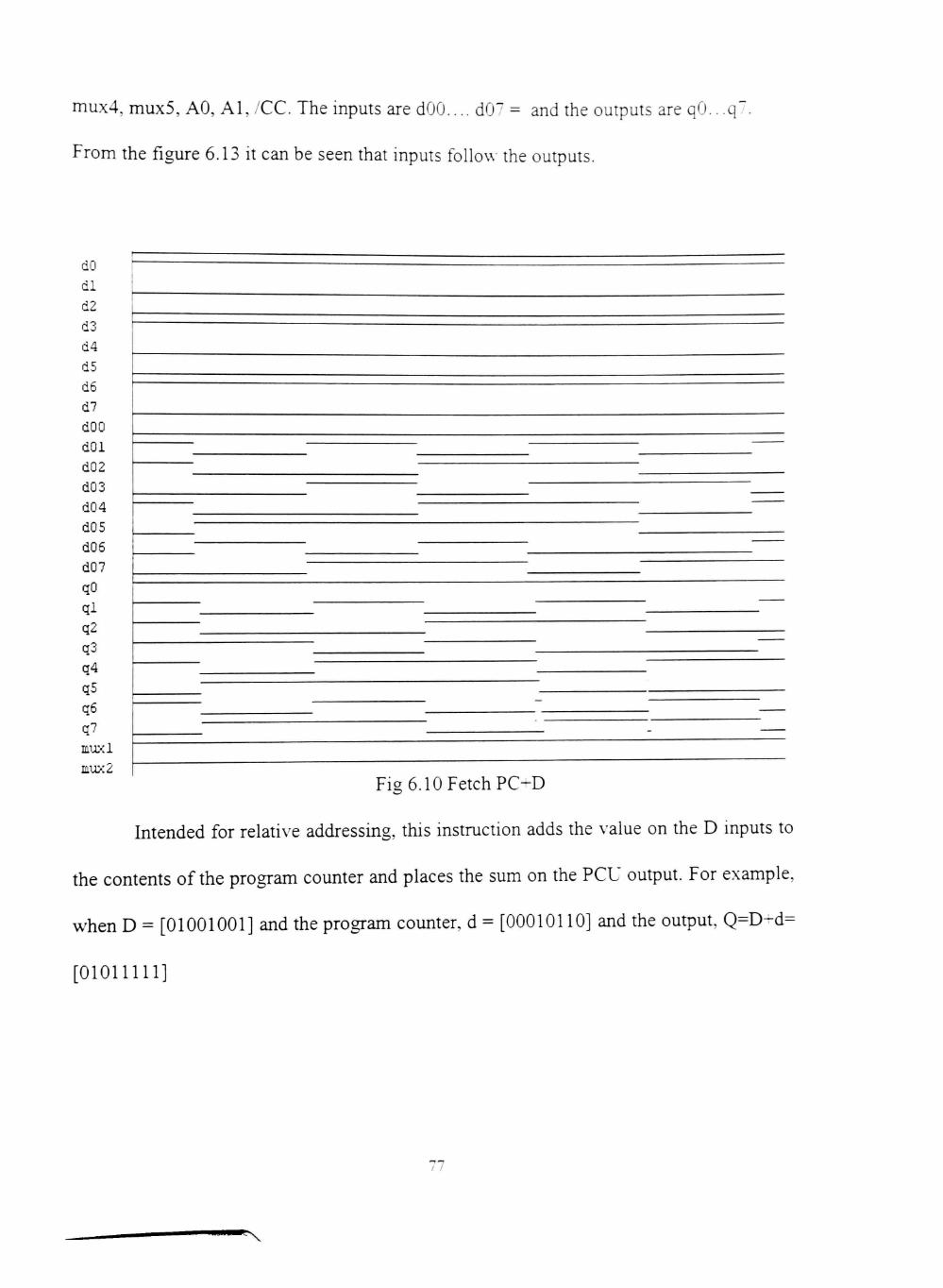
mux4, mux5, AO, Al, /CC. The inputs are dOO.... d07 = and the outputs are q0...q'
From the figure 6.13 it can be seen that inputs follow the outputs.
dO
dl
d2
d3
d4
d5
d6
d7
dOO
dOl
d02
d03
d04
d05
d06
d07
qO
ql q2 q3 q4 q5 q6 q7 mu:<l mu>:2
Fig 6.10 Fetch PC-D
Intended for relative addressmg, this instruction adds the value on the D inputs to
the contents ofthe program counter and places the sum on the PCU output. For example,
when D = [01001001] and the program counter, d = [00010110] and the output, Q=D-d=
[01011111]
77

dOO dOl dOZ d03 d04 do 5 d06 d07 xO x l x2 x3
x5 x6 x7 qO
q l q2 q3 q4 q5 q6 q7 muxl luuxZ
mux 3 miAx4
Fig 6.11 FPR
Intended for relative addressing, this instruction adds the contents ofthe R register to the
contents of the program counter and places the sum on the PCU output. For example,
when R register x = [01000001] and the program counter, D=[d00...d07] = [11011110]
and the output, Q = D + x = [00011111]
78

dOO
dOi
d02
d03
d04
d05
d06
d07
qO
ql
q2
q3
q4
q5
q6
q7
to
tl
t2
t3
t4
tS
t6
t7 ^
' Fig 6.12 Push PC
This instruction places the current value of the program counter on the PCU outputs and
pushes it onto the top ofthe stack. The stack pointer is updated in the process.
[d00....d07] = [1010000] are the contents of PC , [q0...q7] = [1010000] are the output
values on the PCU output. The contents ofthe stack are [t0...t7] = [1010000]. And the
stack pointer is incremented in this process to point to the next memory location on the
stack.
79

dOO
dOl
d02
d03
d04
d05
d06
d07
dO
dl
d2
d3
d4
d5
d6
d7
qO
ql
q2
q3
q4
qS
q6
q7
muxl
mTj:-:2
mux 3
mux 4
mux 5
R_EH
Al
AO
PC_EN
Fig 6.13 JPPD
Intended to implement relative addressing, this instruction adds the value currently on the
D input to the program counter. This results in a relative jump. d00....d07 are the
contents of PC. d0...d7 are the data on the inputs. When /CC=1 it passes the contents of
d00...d07 to the outputs of PCU. From the figure 6.18 it can be seen that [d00...d07] =
80
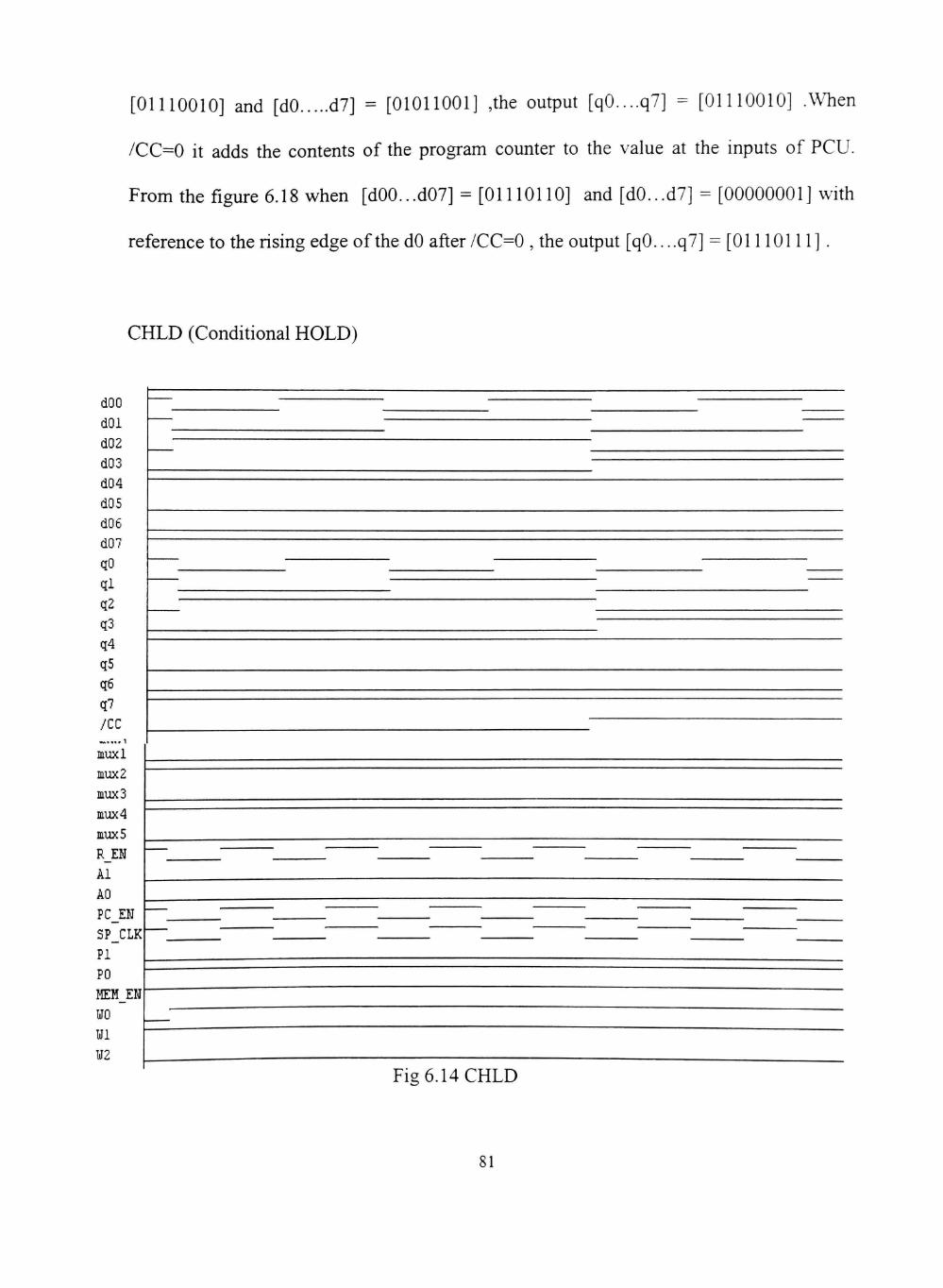
[01110010] and [dO d7] = [01011001] ,the output [q0....q7] = [01110010] .When
/CC=0 it adds the contents of the program counter to the value at the inputs of PCU.
From the figure 6.18 when [d00...d07] = [01110110] and [d0...d7] = [OOOOOOOIJ with
reference to the rising edge ofthe dO after /CC=0 , the output [qO.. ..q7] = [01110111].
CHLD (Conditional HOLD)
dOO
dOl
d02
d03
d04
d05
d06
d07
qO
q l
q2
q3
q4
q5
q6
q7
/CC
muxl
mux 2
mux 3
mux 4
mux 5
R_EN
Al
AO
PC_EJI
SP_CLK
PI
PO
HEH_EN
UO
Ul
¥2
Fig 6.14 CHLD
81

This instruction is a conditional hold, or "no operation" command. The current contents
of the program counter are placed on the outputs of the PCU. The current contents of the
PC, R and stack are not affected. If the output of the CCR is enabled, the instruction is
conditional. From the fig 6.19 the contents ofthe PC are [d00...d07] = [10010011]. The
outputs are denoted by [q0...q7] = [10010011] . And /CC is the output of CCR.The
contents ofthe stack pointer wO, wl,w2 are not changed.
6.3 Lavout level Testing
The layout for each individual component has been drawn and simulation results
have been found in agreement with the results from gate level simulations. But simulation
of the entire unit at layout level has not done due to the fact it would require excessive
simulation time and would be difficult to interpret.
82

CHAPTER VII
CONCLUSIONS
7.1 Conclusion
Any large-scale digital design expects to achieve the following objective
• Simplicity in design,
• Lower cost,
• Higher reliability (stability of outputs at desired clock speeds),
• Shorter design time and flexibility.
All the above are the fine points of this design endeavor. The logic design was
made as simple and straight forward as possible because simplicity is one ofthe
important criteria of modular design (building block). The simulation tool- Logic Works
that was used is also low cost, which is also in the best interest of any digital design of
this size.
This is a LSI level design, as the number of transistors used for the design can be
estimated to be above 3500-4000. This unit offers flexibility in various applications. In
broader terms it performs sequential, conditional and unconditional branching, and
subroutine control flows. It can be cascaded for any higher number of bits such as 16, 24,
32 bits.
One ofthe important disadvantages of modular based designs is low speed. As a
single module on its own, it can perform fast operations, but when cascaded speed is
83

sacrificed to achieve a bigger unit. But the program control unit is designed as a
synchronous
sequential logic system, where signals that affect the system are employed at discrete
instants of time. And the inputs to the are applied . So there is considerable reduction in
the loss of speed ofthe system as whole. The design has eight input pins, eight output
pins, and eleven control pins. This unit can be easily cascaded or used as part of a larger
design Hence the module achieves shorter design time and higher flexibility when
instituted as part of a bigger design.
7.2 Future Work
The hardware implementation and layout of the Program Control Unit has been
successfiilly achieved. The module can be made completely fianctional by using it as a
block in the microprocessor design.
84

REFERENCES
1. White, E. D, Logic Design for Array-Based Circuit, 1992, Academic Press, Inc., San Diego California.
2. Mano, M. M., Computer System Architecture, 1993, Prentice-Hall, Inc., Englewood Cliffs, N J.
3. Smith, Michael John Sebastian, Application-Specific Integrated Circuits, 1997, Addison-Wesley Publishing Company, Menlo Park, California.
4. Uyemura, J. P., Physical design of CMOS Integrated Circuits Using L-Edit™, 1998, PWS Publishing Company, Boston Massachusetts.
5. Carter, J. W., Microprocessor Architecture and Microprogramming: A state machine approach, 1996, Prentice Hall, Englewood Cliffs, NJ.
6. Uyemura, J. P., Physical design of CMOS Integrated Circuits Using L-Edit''^', 1998, PWS Publishing Company, Boston Massachusetts.
7. Rabaey, J. M., Digital Integrated circuits: a design perspective, 1996, Prentice-Hall Inc., Englewood Cliffs, N J.
8. Abraham, K. Bobby, "8-bit Micro Controller" Master Thesis, Texas Tech University, 1998.
9. Reddy, M. Pavan "Modular Arithmetic Logic Unit Controller" Master Thesis, Texas Tech University, 1999.
85