modulation and signal generation with r&s® signal ... · 2.1.4 angle modulation ... amplitude...
TRANSCRIPT

Modulation and Signal Generation with R&S® Signal Generators Educational Note
Products:
ı R&S®SMB100A
ı R&S®SMBV100A
ı R&S®SMC
ı HM8134-3/HM8135
ı HMF2525 / HMF2550
Signal generators play a vital role in electrical test and measurement. They generate the test signals that
are applied to components such as filters and amplifier, or even to entire modules, in order to ascertain and
test their behavior and characteristics. The first part of this educational note presents the applications for
and the most important types of signal generators. This is followed by a description of the construction and
functioning of analog and vector signal generators. To permit a better understanding of the specifications
found on data sheets, a closer look at the most important parameters for a signal generator is provided.
Beyond the output of spectrally pure signals, a key function of RF signal generators is the generation of
analog- and digitally modulated signals. The second part of this note therefore presents the fundamentals
for the most significant analog and digital modulation methods.
The third part of this educational note contains exercises on the topics of analog and digital modulation. All
described measurements were performed using the R&S®SMBV100A vector signal generator and the
R&S®FSV spectrum analyzer.
Note:
The most current version of this document is available on our homepage:
http://www.rohde-schwarz.com/appnote/1MA225.
R. W
agne
r, M
. Rei
l
8.20
16 1
MA
225-
2e
Edu
catio
nal N
ote

Contents
1MA225-2e Rohde & Schwarz Modulation and Signal Generation with R&S® Signal Generators
2
Contents
1 What Is a Signal Generator? .............................................................. 4
1.1 Why Do We Need Signal Generators? ....................................................................... 4
1.2 What Types of Signal Generators Are Available? .................................................... 5
1.2.1 Analog Signal Generators .............................................................................................. 5
1.2.2 Vector Signal Generators ............................................................................................19
1.2.3 Arbitrary Waveform Generators (ARBs) ......................................................................33
1.3 Key Signal Generator Characteristics .....................................................................36
1.3.1 Phase Noise .................................................................................................................36
1.3.2 Spurious Emissions .....................................................................................................41
1.3.3 Frequency Stability ......................................................................................................46
1.3.4 Level Accuracy and Level Setting Time ......................................................................47
1.3.5 Error Vector Magnitude (EVM) ....................................................................................48
1.3.6 Adjacent Channel Power (ACP) ..................................................................................50
1.3.7 Impedance Matching (VSWR) .....................................................................................51
2 Modulation Methods ......................................................................... 57
2.1 Analog Modulation Methods .....................................................................................57
2.1.1 Amplitude Modulation ..................................................................................................58
2.1.2 Time Function and Frequency Spectrum of Amplitude Modulation .............................58
2.1.3 Types of Amplitude Modulation ...................................................................................64
2.1.4 Angle Modulation .........................................................................................................67
2.1.5 Time Function and Frequency Spectrum.....................................................................67
2.1.6 Differentiation of Frequency versus Phase Modulation in Angle Modulation ..............71
2.1.7 Frequency Modulation with Predistortion ....................................................................72
2.1.8 Pros and Cons of Frequency Modulation versus Amplitude Modulation .....................73
2.2 Digital Modulation Methods ......................................................................................74
2.3 Principles of I/Q Modulation .....................................................................................75
2.4 Digital Modulation of a Sine-Wave Carrier ..............................................................77
2.4.1 Amplitude Shift Keying (ASK) ......................................................................................77
2.4.2 Frequency Shift Keying (FSK) .....................................................................................78
2.4.3 Phase Shift Keying (PSK) ............................................................................................82
2.4.4 Quadrature Amplitude Modulation (QAM) ...................................................................88
2.4.5 Comparing Different Phase Shift Keying Methods ......................................................91
2.4.6 Crest Factor / Linearity Requirements .........................................................................92
2.5 Access Methods.........................................................................................................93
3 Exercises ........................................................................................... 95
Contents
1MA225-2e Rohde & Schwarz Modulation and Signal Generation with R&S® Signal Generators
3
3.1 Amplitude Modulation ...............................................................................................95
3.1.1 Test Setup ....................................................................................................................95
3.1.2 Measurement ...............................................................................................................96
3.2 Frequency Modulation ..............................................................................................99
3.2.1 Test Setup ....................................................................................................................99
1.1 Measurement ..............................................................................................................99
3.3 Digital Modulation Exercises ..................................................................................103
3.3.1 Test Setup ..................................................................................................................104
3.3.2 Instrument Configurations ..........................................................................................104
3.3.3 Measuring Digital Signals ..........................................................................................107
3.4 Frequency Response Measurement ......................................................................118
3.4.1 Test Setup ..................................................................................................................118
3.4.2 Measurement .............................................................................................................119
4 Literature ......................................................................................... 123

What Is a Signal Generator?
1MA225-2e Rohde & Schwarz Modulation and Signal Generation with R&S® Signal Generators
4
1 What Is a Signal Generator?
A signal generator generates electrical signals with a specific time characteristic.
Depending on the type of signal generator, the generated signal waveforms can range
from simple sine-wave, sawtooth and square-wave to analog-modulated signals such
as AM, FM and PM and even complex digitally modulated signals such as those used
in mobile radio (GSM, UMTS, LTE, etc.). The frequency domain can extend from
several kHz into the two-digit GHz range. By adding external frequency multipliers, it is
even possible to obtain signal frequencies up to several hundred GHz. The frequency
of the output signal can typically be set in very small steps (< 1 Hz).
The RF generators used in the automated test setups for production can be remotely
controlled via a LAN connection, a USB port or a GPIB port, depending on the
available equipment.
RF signal generators are classified into two main types:
ı Analog signal generators and
ı Vector signal generators
1.1 Why Do We Need Signal Generators?
Signal generators are primarily used in the development and production of electronic
modules and components. The signal produced by the signal generator is fed to an RF
module (amplifier, filter, etc.) under test. The output signal from the module is then
analyzed using an appropriate test instrument such as a spectrum or signal analyzer,
oscilloscope, power meter, etc. (Fig. 1-1). Based on the results of this analysis, it is
possible to determine whether the module exhibits the expected behavior. In addition
to the typical settings for frequency, amplitude and modulation mode, state-of-the-art
signal generators also offer the ability to add noise to the test signal or to simulate
multipath propagation (fading) of the input signal. This makes it possible to study the
behavior of a receiver with very noisy receive signals that also reach the receiver via
multipath propagation.
Although signal generators are not a test instrument in the strictest sense, they are still
considered to be test transmitters because of the use case described above.
Fig. 1-1: The signal generator supplies the test signal for the functional test of the connected DUT.
What Is a Signal Generator?
1MA225-2e Rohde & Schwarz Modulation and Signal Generation with R&S® Signal Generators
5
1.2 What Types of Signal Generators Are Available?
The selection of the correct signal generator is always dependent on the application.
Important criteria include frequency domain, level range, spectral purity, available
modulations (analog, digital) and functionality for adding specific interference to signals
(noise, simulated multipath propagation).
Simple signal generators for the low-frequency range are called tone generators.
Typically, a tone generator produces a sine-wave, square-wave or sawtooth electrical
signal in the human-audible frequency range, i.e. 20 Hz to 20,000 Hz. The output
signal can be set manually both in frequency and in amplitude. Tone frequency
generators are most often used for acoustical test and measurement and for electro-
acoustics in combination with an appropriate audio level meter. This makes it possible
to determine whether the generated test tone passes through a tone transmitter
system at the desired level, for example. For sweep measurements, a suitable level
meter (e.g. oscilloscope, spectrum analyzer, power meter) can additionally be used to
acquire the full frequency response of a transmission system by continually shifting the
output frequency or by using a spectrum analyzer to supply the frequency.
Signal generators that produce only simple, periodic signals are called function
generators. This typically includes sine-wave, square-wave and triangle oscillations.
Today's function generators are overwhelmingly digital. These operate using direct
digital synthesis (DDS) (see also section 1.2.1.1 ) and can produce a variety of periodic
signal traces. Example function generators applications include the assessment of
electronic circuits such as amplifiers and filters.
HF-signal generators used to produce high-frequency sine-wave oscillations. These
often include a sweep function that permits repetitive sweeps through an adjustable
frequency domain. The frequency domain can extend from several kHz into the two-
digit GHz range. RF generators are categorized as either analog or vector signal
generators. Analog signal generators permit analog modulation of the output signal in
frequency and amplitude. They are also capable of producing pulsed signals. Vector
signal generators are additionally capable of producing digitally modulated signals for a
variety of standards from mobile radio, digital radio and TV and so on. Like analog
signal generators, vector signal generators also modulate a high-frequency carrier
signal.
Arbitrary waveform generators (ARBs) are vector signal generators for which the
modulation data is calculated in advance (rather than in realtime) and stored in the
instrument's RAM. The output signal is always a baseband signal. The advantage of
these generators is that they can produce and repeat almost any conceivable
waveform as often as necessary. ARBs are used as a universal signal source in
development, research, test and service.
The following section of this educational note provides a closer look at RF signal
generators (analog, vector-modulated) and at arbitrary waveform generators.
1.2.1 Analog Signal Generators
With analog signal generators, the focus is on producing a high-quality RF signal. They
provide support for the analog modulation modes AM / FM and φM. Many instruments
can also produce precise pulsed signals with varying characteristics.

What Is a Signal Generator?
1MA225-2e Rohde & Schwarz Modulation and Signal Generation with R&S® Signal Generators
6
Analog generators are available for frequencies extending up to the microwave range.
In addition to a frequency sweep over an adjustable frequency range, a few
instruments also can do a level sweep through the output levels within predefined
limits. This makes it possible to produce some of the same waveforms as a function
generator, such as sawtooth or triangle.
As mentioned, levels with a previously defined pulse/pause ratio can output a repetitive
sequence of square-wave amplitude characteristics. Analog generators typically exhibit
the following characteristics:
ı Very high spectral purity (nonharmonics), e.g. –100 dBc
ı Very low inherent broadband noise, e.g. –160 dBc
ı Very low SSB phase noise of typ. –140 dBc/Hz (at 10 kHz carrier spacing,
f = 1 GHz, 1 Hz measurement bandwidth)
Analog signal generators are used:
ı As a stable reference signal for use as a local oscillator, i.e. as a source for phase
noise measurements or as a calibration reference.
ı As a universal instrument for measuring gain, linearity, bandwidth, etc.
ı In the development and testing of RF chips and other semiconductor chips, such
as those used for A/D converters
ı For receiver tests (two-tone tests, generation of interferer and blocking signals)
ı For electromagnetic compatibility (EMC) testing
ı As automatic test equipment (ATE) during production
ı For avionics applications (such as VOR, ILS)
ı For radar tests
ı For military applications
Fig. 1-2 shows an example of a special impulse sequence for radar applications:
Fig. 1-2: Combination of impulses with different widths and interpulse periods for radar applications.
Analog signal generators are available with different specifications in all price classes.
The criteria listed in section 1.3 Key Signal Generator Characteristics can be used to
select an appropriate model. Some typical characteristics include a specific output
power level, rapid frequency and level settling, a defined degree of level and frequency
accuracy, a low VSWR or even the design and weight of the generator.

What Is a Signal Generator?
1MA225-2e Rohde & Schwarz Modulation and Signal Generation with R&S® Signal Generators
7
1.2.1.1 Design and functioning of an analog signal generator
Fig. 1-3 shows the basic design of an analog RF signal generator. A signal generator consists of three main functional blocks:
ı A synthesizer for producing the oscillation
ı An automatic level control for maintaining a constant output level
ı An output stage with amplifiers and step attenuators for controlling the output
power
Fig. 1-3: Schematic diagram of an analog RF signal generator.
Synthesizer:
The core of the generator is the synthesizer used to produce the oscillations. The term
synthesizer describes a functional principle in which oscillations are synthetically
derived by means of division and multiplication from the oscillations of a crystal with a
fixed reference frequency (reference oscillator). Usually a signal generator can also be
synchronized to an applied reference frequency via a reference frequency input. This
permits synchronization with other test instruments, such as a spectrum analyzer.
Because a frequency from a crystal provides long-term stability and low dependence
on temperature, crystal oscillators are used to generate the reference frequency. The
quality of an oscillator is typically assessed based on the stability of its amplitude,
frequency and phase. The stability can be increased further by using a temperature-
controlled crystal oscillator (TCXO). This consists of a voltage-controlled oscillator
(VCO) and a compensation circuit that compensates for the oscillator's temperature
dependency. The frequency accuracy of these oscillators is under 100 ppm (ppm:
What Is a Signal Generator?
1MA225-2e Rohde & Schwarz Modulation and Signal Generation with R&S® Signal Generators
8
parts per million, i.e.10–6
), making them up to ten thousand times more accurate than
an LC resonant circuit built from discrete components. Nevertheless, a TCXO always
retains a small thermal frequency drift that is disruptive for precision applications. To
further improve the frequency accuracy, most signal generators also offer an oven-
controlled crystal oscillator (OCXO) as an option. In an OCXO, the crystal oscillator is
located in a heated, temperature-controlled chamber. By regulating the temperature of
the oscillating crystal and the oscillator circuit to a value above room temperature, it is
possible to further stabilize the oscillation frequency, providing a higher degree of
accuracy than without heating. Depending on the type of oscillator used and the
application, the operating temperature lies in the range from +30 °C to +85 °C. This
provides a level of accuracy a thousand times better than that of a TCXO, in the range
of 0.001 ppm, or 10–9
. The frequency drift caused by aging of the oscillator is also
improved. In this case, the improvement is a factor of 100, from 10–6
/ year to 10–8
/
year. Because aging of the reference oscillator is unavoidable, a regular adjustment of
the reference frequency might be necessary in order to ensure a high absolute
accuracy, depending on the application.
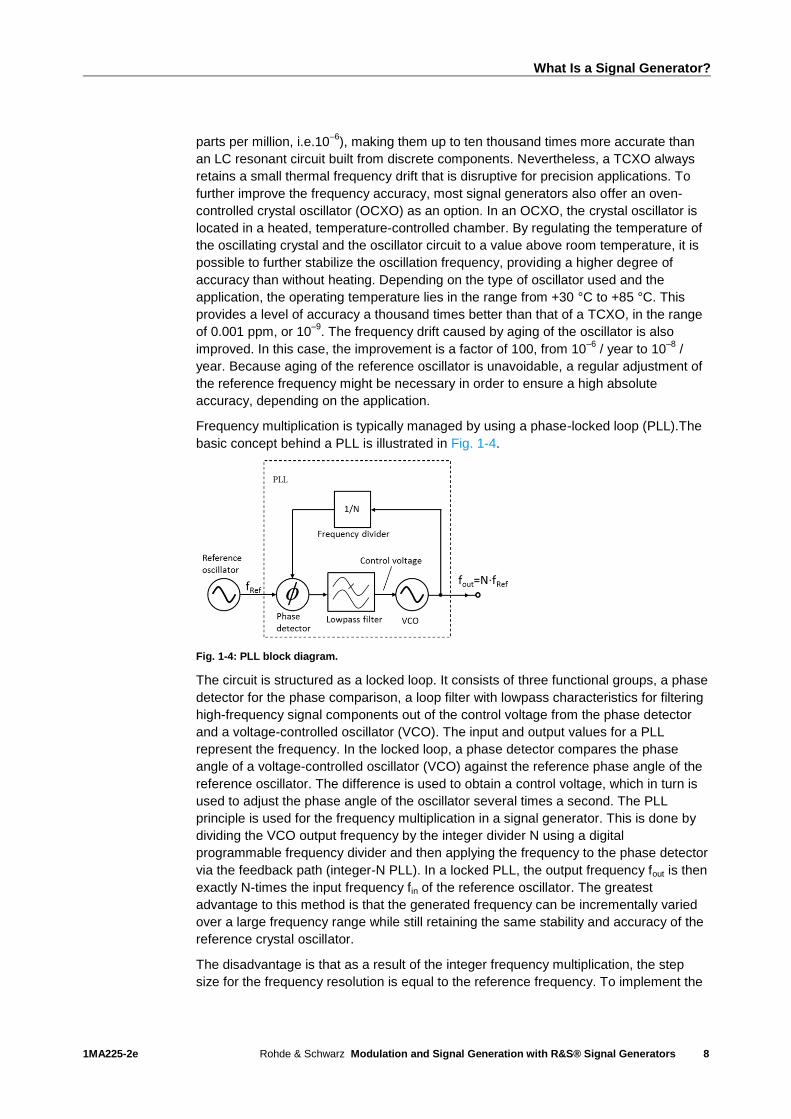
Frequency multiplication is typically managed by using a phase-locked loop (PLL).The
basic concept behind a PLL is illustrated in Fig. 1-4.
Fig. 1-4: PLL block diagram.
The circuit is structured as a locked loop. It consists of three functional groups, a phase
detector for the phase comparison, a loop filter with lowpass characteristics for filtering
high-frequency signal components out of the control voltage from the phase detector
and a voltage-controlled oscillator (VCO). The input and output values for a PLL
represent the frequency. In the locked loop, a phase detector compares the phase
angle of a voltage-controlled oscillator (VCO) against the reference phase angle of the
reference oscillator. The difference is used to obtain a control voltage, which in turn is
used to adjust the phase angle of the oscillator several times a second. The PLL
principle is used for the frequency multiplication in a signal generator. This is done by
dividing the VCO output frequency by the integer divider N using a digital
programmable frequency divider and then applying the frequency to the phase detector
via the feedback path (integer-N PLL). In a locked PLL, the output frequency fout is then
exactly N-times the input frequency fin of the reference oscillator. The greatest
advantage to this method is that the generated frequency can be incrementally varied
over a large frequency range while still retaining the same stability and accuracy of the
reference crystal oscillator.
The disadvantage is that as a result of the integer frequency multiplication, the step
size for the frequency resolution is equal to the reference frequency. To implement the
What Is a Signal Generator?
1MA225-2e Rohde & Schwarz Modulation and Signal Generation with R&S® Signal Generators
9
smallest frequency resolution steps possible, the frequency of the reference oscillator
can be divided down accordingly before the PLL by using a frequency divider. In order
to produce high frequencies, the resulting small steps make it necessary to select an
appropriate lager dividing factor N (works as a multiplier at the output of the PLL). This
in turn negatively affects the phase noise (see also section 1.3.1) of the output signal,
which increases by 20 log (N) dB. In the case of a signal generator with a step size of
100 kHz and a maximum generator frequency of 1 GHz, the phase noise up to 1 GHz
increases by 20 log (10000) dB = 80 dB. Lower reference frequencies additionally
require a narrow control bandwidth. The lock time depends primarily on the control
bandwidth. The smaller this is, the slower the PLL becomes.
In order to counteract the above-mentioned disadvantages of lager dividing factors and
the associated worsening of the phase noise, synthesizers can be equipped with
multiple PLLs as shown in Fig. 1-5.
Fig. 1-5: Multiloop synthesizer (multi-PLL).
To implement fine frequency steps, a frequency divider is placed in the upper signal
path at the output of the first PLL (PLL1). Larger frequency steps are generated in the
lower path by means of a second PLL (PLL2). At the output of yet another PLL (PLL3),
which contains a mixer in the feedback path instead of a frequency divider, the output
frequency with the dividing factors N1, N2 and M is described by the following equation:
Equation 1-1:
𝑓𝑜𝑢𝑡 = 𝑓𝑟𝑒𝑓 ∙ (𝑁1
𝑀+ 𝑁2)
For example, if N1 = 100, M = 100 and N2 = 99, at a reference frequency fref = 10 MHz
the above equation generates an output frequency of 1 GHz (fout = 1 GHz ). The
minimum step size is 100 kHz. In comparison to the simple PLL shown in Fig. 1-4, the
significantly smaller divider values result in a lower phase noise for the output signal. In
addition, from Equation 1-1 it becomes clear that with a multi-PLL, the appropriate
selection of N1 and M can also result in fractional factors for the frequency
multiplication, and therefore very small frequency steps. The disadvantage of a multi-
What Is a Signal Generator?
1MA225-2e Rohde & Schwarz Modulation and Signal Generation with R&S® Signal Generators
10
PLL is that a stable output signal requires that all PLLs be locked, which makes
extremely short frequency settling times impossible.
In summary, when dimensioning an integer-N PLL, a high frequency resolution stands
in opposition to the requirements for spectral purity and short lock times. A multi-PLL
delivers small step sizes with low phase noise. However, the frequency settling time is
not adequate for many applications, such as production environments.
In order to achieve a faster settling time, modern signal generators therefore add a
frequency divider to the feedback path of a PLL, which divides the VCO frequency
using fractional factors (see Fig. 1-3).
To do this, the dividing factors of various integer values are varied over time so that
they average value is equal to the desired fractional value. For example, to achieve an
divider of 100.5, one half of the time is divided by 100 and the remaining time by 101.
This averages out to the desired value of 100.5. Control loops that operate on this
principle are called fractional-N PLLs or fractional-N synthesizers. However, fractional
spurs are generated at the output of the phase detector that must be compensated for
or filtered out by using appropriate countermeasures (Delta-Sigma method). Fractional-
N synthesizers can provide infinitely fine frequency resolutions with simultaneously
short settling times and very high spectral purity. For further reduction of the phase
noise, fractional-N synthesizers are also implemented as multiloop fractional-N
synthesizers following the principle shown in Fig. 1-5.
Particularly low phase noise synthesizers are implemented based on the direct digital
synthesis (DDS) concept. This concept has its foundation in a method taken from
digital signal processing for the generation of periodic, band-limited signals with
infinitely fine frequency resolution. Next to PLL, DDS is the most important method
today for generating signals with finely adjustable frequencies into the mHz range, and
as such has found wide usage in the test and measurement field.
Because D/A converters are not yet available for generating high frequencies, the DDS
concept is limited to clock frequencies up to around 1 GHz. In signal generators
(function generators) for the frequency range up to several hundred MHz, DDS is often
the only signal generation method in use. To utilize the advantages offered by PLL
synthesizers and DSS, signal generators for higher frequencies often use a
combination of the two methods.
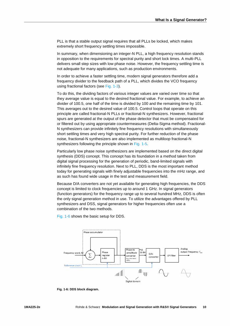
Fig. 1-6 shows the basic setup for DDS.
Fig. 1-6: DDS block diagram.
What Is a Signal Generator?
1MA225-2e Rohde & Schwarz Modulation and Signal Generation with R&S® Signal Generators
11
DDS is based on a phase accumulator that consists of a digital accumulator combined
with a register, including a feedback path. The register functions as storage for the
current phase angle. For each clock step, this phase accumulator adds the applied
frequency word via the feedback path and the phase register, and thus functions as a
counter. The digital frequency word, at a length ranging from 24 bits to 48 bits, is
equivalent to the desired output frequency. The instantaneous count corresponds to a
specific phase angle. The phase accumulator can also be viewed as a digital phase
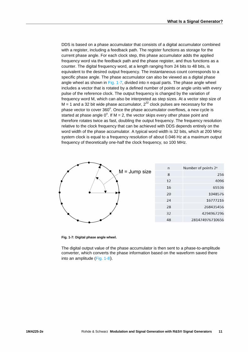
angle wheel as shown in Fig. 1-7, divided into n equal parts. The phase angle wheel
includes a vector that is rotated by a defined number of points or angle units with every
pulse of the reference clock. The output frequency is changed by the variation of
frequency word M, which can also be interpreted as step sizes. At a vector step size of
M = 1 and a 32 bit wide phase accumulator, 232
clock pulses are necessary for the
phase vector to cover 360o. Once the phase accumulator overflows, a new cycle is
started at phase angle 0o. If M = 2, the vector skips every other phase point and
therefore rotates twice as fast, doubling the output frequency. The frequency resolution
relative to the clock frequency that can be achieved with DDS depends entirely on the
word width of the phase accumulator. A typical word width is 32 bits, which at 200 MHz
system clock is equal to a frequency resolution of about 0.046 Hz at a maximum output
frequency of theoretically one-half the clock frequency, so 100 MHz.
Fig. 1-7: Digital phase angle wheel.
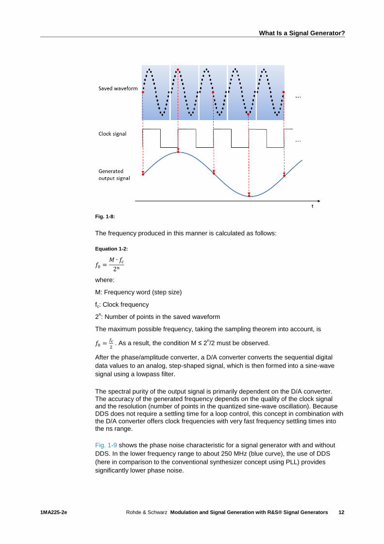
The digital output value of the phase accumulator is then sent to a phase-to-amplitude converter, which converts the phase information based on the waveform saved there
into an amplitude (Fig. 1-8).
M = Jump size
What Is a Signal Generator?
1MA225-2e Rohde & Schwarz Modulation and Signal Generation with R&S® Signal Generators
12
Fig. 1-8:
The frequency produced in this manner is calculated as follows:
Equation 1-2:
𝑓0 =𝑀 ∙ 𝑓𝑐
2𝑛
where:
M: Frequency word (step size)
fc: Clock frequency
2n: Number of points in the saved waveform
The maximum possible frequency, taking the sampling theorem into account, is
𝑓0 =𝑓𝑐
2 . As a result, the condition M ≤ 2
n/2 must be observed.
After the phase/amplitude converter, a D/A converter converts the sequential digital
data values to an analog, step-shaped signal, which is then formed into a sine-wave
signal using a lowpass filter.
The spectral purity of the output signal is primarily dependent on the D/A converter. The accuracy of the generated frequency depends on the quality of the clock signal and the resolution (number of points in the quantized sine-wave oscillation). Because DDS does not require a settling time for a loop control, this concept in combination with the D/A converter offers clock frequencies with very fast frequency settling times into the ns range.
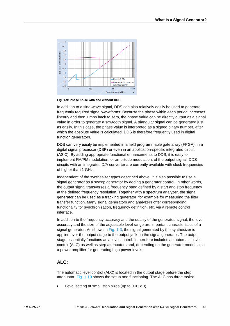
Fig. 1-9 shows the phase noise characteristic for a signal generator with and without
DDS. In the lower frequency range to about 250 MHz (blue curve), the use of DDS
(here in comparison to the conventional synthesizer concept using PLL) provides
significantly lower phase noise.
What Is a Signal Generator?
1MA225-2e Rohde & Schwarz Modulation and Signal Generation with R&S® Signal Generators
13
Fig. 1-9: Phase noise with and without DDS.
In addition to a sine-wave signal, DDS can also relatively easily be used to generate
frequently required signal waveforms. Because the phase within each period increases
linearly and then jumps back to zero, the phase value can be directly output as a signal
value in order to generate a sawtooth signal. A triangular signal can be generated just
as easily. In this case, the phase value is interpreted as a signed binary number, after
which the absolute value is calculated. DDS is therefore frequently used in digital
function generators.
DDS can very easily be implemented in a field programmable gate array (FPGA), in a
digital signal processor (DSP) or even in an application-specific integrated circuit
(ASIC). By adding appropriate functional enhancements to DDS, it is easy to
implement FM/PM modulation, or amplitude modulation, of the output signal. DDS
circuits with an integrated D/A converter are currently available with clock frequencies
of higher than 1 GHz.
Independent of the synthesizer types described above, it is also possible to use a
signal generator as a sweep generator by adding a generator control. In other words,
the output signal transverses a frequency band defined by a start and stop frequency
at the defined frequency resolution. Together with a spectrum analyzer, the signal
generator can be used as a tracking generator, for example for measuring the filter
transfer function. Many signal generators and analyzers offer corresponding
functionality for synchronization, frequency definition, etc. via a remote control
interface.
In addition to the frequency accuracy and the quality of the generated signal, the level
accuracy and the size of the adjustable level range are important characteristics of a
signal generator. As shown in Fig. 1-3, the signal generated by the synthesizer is
applied over the output stage to the output jack on the signal generator. The output
stage essentially functions as a level control. It therefore includes an automatic level
control (ALC) as well as step attenuators and, depending on the generator model, also
a power amplifier for generating high power levels.
ALC:
The automatic level control (ALC) is located in the output stage before the step attenuator. Fig. 1-10 shows the setup and functioning. The ALC has three tasks:
ı Level setting at small step sizes (up to 0.01 dB)

What Is a Signal Generator?
1MA225-2e Rohde & Schwarz Modulation and Signal Generation with R&S® Signal Generators
14
ı Constant maintenance of the level over temperature and time
ı Amplitude modulation (AM) through changes to the input variable
Fig. 1-10: Automatic level control (ALC) setup.
For the level control the synthesizer signal is supplied to a pin-diode modulator. The
PIN diode represents a DC-controlled resistance for higher frequencies that is used to
control the signal amplitude. The subsequent switchable lowpass filters serve to
suppress harmonics. The following amplifier compensates the insertion loss of the
modulator. Harmonics that lie above the maximum output frequency of the synthesizer
are subsequently suppressed with a lowpass filter. In the case of an ALC, a control
loop constantly maintains the output signal at a defined value. The control is
implemented by using a directional coupler with a known coupling loss behavior to
uncouple a portion of the output signal, which is then applied to a detector diode. An
ALC amplifier in the feedback path compares the reference voltage Vref that is equal to
the defined level against the actual voltage Vact. From the difference between the two
voltages, the correction DC voltage is derived in order to control the PIN diode. An ALC
makes a very precise electronic level attenuation up to 40 dB possible, for example
from –15 dBm to +25 dBm, along with small step sizes down to 0.01 dB. With an ALC,
a change in the control voltage (Vref) based on the wanted signal can very easily
generate an amplitude-modulated oscillation.
For most applications, the ALC is typically switched on. In the case of pulse-modulated
signals, however, an ALC would lead to level variations in the output pulse sequence.
Therefore, signal generators with ALC include the option of switching it off. Another set
of applications in which ALC negatively affects the measurements are multitone
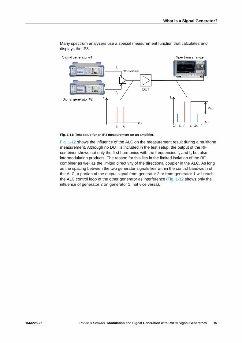
measurements with two signal generators. Fig. 1-11 shows a multitone measurement
for determining the third harmonic intercept point (IP3) of an amplifier. Two signals of
equal level are sent to the amplifier with different frequencies f1 and f2 via an RF
combiner. The output spectrum of the amplifier is determined using a spectrum
analyzer. From the third intermodulation ratio aIM3 (level offset between the first
harmonic and the third intermodulation product), it is possible to calculate the IP3.
What Is a Signal Generator?
1MA225-2e Rohde & Schwarz Modulation and Signal Generation with R&S® Signal Generators
15
Many spectrum analyzers use a special measurement function that calculates and
displays the IP3.
Fig. 1-11: Test setup for an IP3 measurement on an amplifier.
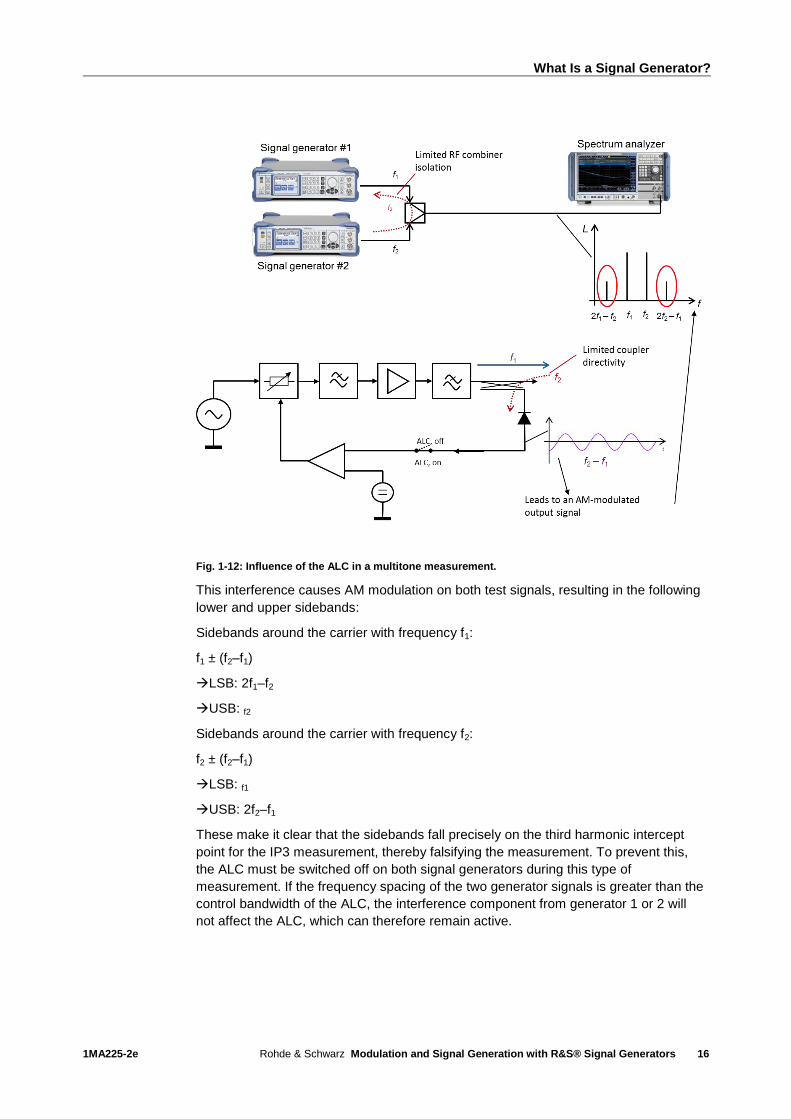
Fig. 1-12 shows the influence of the ALC on the measurement result during a multitone
measurement. Although no DUT is included in the test setup, the output of the RF
combiner shows not only the first harmonics with the frequencies f1 and f2 but also
intermodulation products. The reason for this lies in the limited isolation of the RF
combiner as well as the limited directivity of the directional coupler in the ALC. As long
as the spacing between the two generator signals lies within the control bandwidth of
the ALC, a portion of the output signal from generator 2 or from generator 1 will reach
the ALC control loop of the other generator as interference (Fig. 1-12 shows only the
influence of generator 2 on generator 1, not vice versa).
What Is a Signal Generator?
1MA225-2e Rohde & Schwarz Modulation and Signal Generation with R&S® Signal Generators
16
Fig. 1-12: Influence of the ALC in a multitone measurement.
This interference causes AM modulation on both test signals, resulting in the following
lower and upper sidebands:
Sidebands around the carrier with frequency f1:
f1 ± (f2–f1)
LSB: 2f1–f2
USB: f2
Sidebands around the carrier with frequency f2:
f2 ± (f2–f1)
LSB: f1
USB: 2f2–f1
These make it clear that the sidebands fall precisely on the third harmonic intercept
point for the IP3 measurement, thereby falsifying the measurement. To prevent this,
the ALC must be switched off on both signal generators during this type of
measurement. If the frequency spacing of the two generator signals is greater than the
control bandwidth of the ALC, the interference component from generator 1 or 2 will
not affect the ALC, which can therefore remain active.
What Is a Signal Generator?
1MA225-2e Rohde & Schwarz Modulation and Signal Generation with R&S® Signal Generators
17
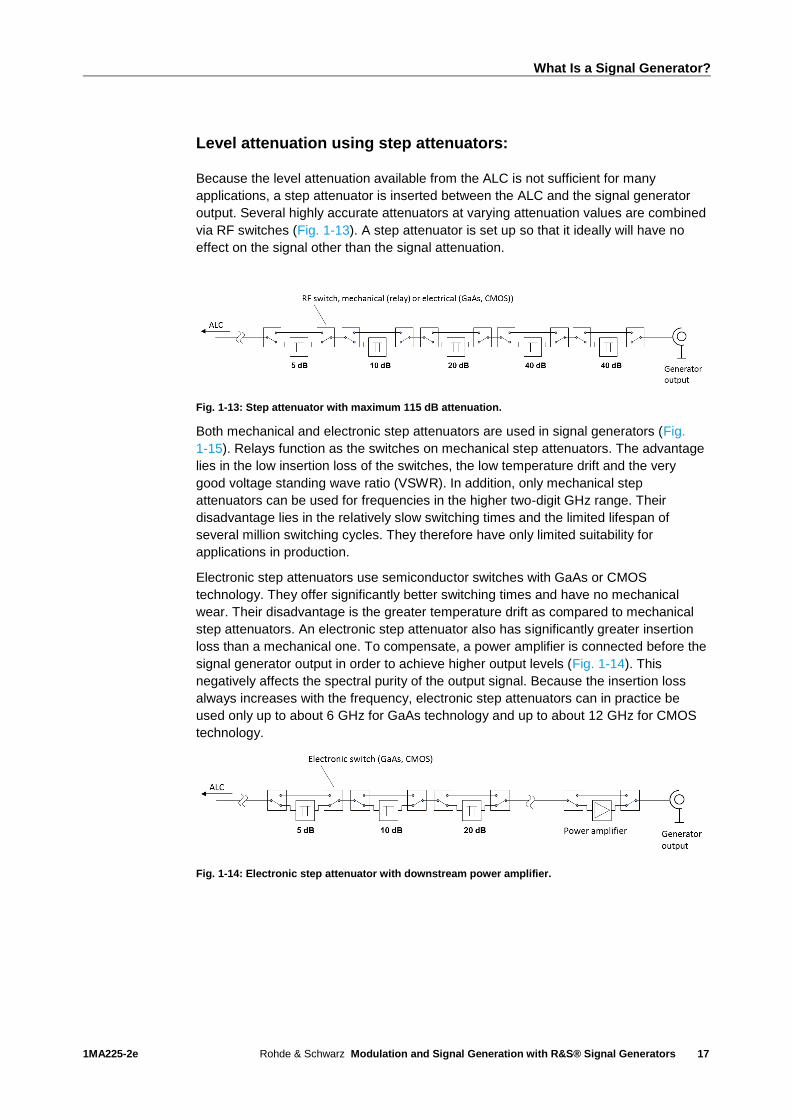
Level attenuation using step attenuators:
Because the level attenuation available from the ALC is not sufficient for many
applications, a step attenuator is inserted between the ALC and the signal generator
output. Several highly accurate attenuators at varying attenuation values are combined
via RF switches (Fig. 1-13). A step attenuator is set up so that it ideally will have no
effect on the signal other than the signal attenuation.
Fig. 1-13: Step attenuator with maximum 115 dB attenuation.
Both mechanical and electronic step attenuators are used in signal generators (Fig.
1-15). Relays function as the switches on mechanical step attenuators. The advantage
lies in the low insertion loss of the switches, the low temperature drift and the very
good voltage standing wave ratio (VSWR). In addition, only mechanical step
attenuators can be used for frequencies in the higher two-digit GHz range. Their
disadvantage lies in the relatively slow switching times and the limited lifespan of
several million switching cycles. They therefore have only limited suitability for
applications in production.
Electronic step attenuators use semiconductor switches with GaAs or CMOS
technology. They offer significantly better switching times and have no mechanical
wear. Their disadvantage is the greater temperature drift as compared to mechanical
step attenuators. An electronic step attenuator also has significantly greater insertion
loss than a mechanical one. To compensate, a power amplifier is connected before the
signal generator output in order to achieve higher output levels (Fig. 1-14). This
negatively affects the spectral purity of the output signal. Because the insertion loss
always increases with the frequency, electronic step attenuators can in practice be
used only up to about 6 GHz for GaAs technology and up to about 12 GHz for CMOS
technology.
Fig. 1-14: Electronic step attenuator with downstream power amplifier.

What Is a Signal Generator?
1MA225-2e Rohde & Schwarz Modulation and Signal Generation with R&S® Signal Generators
18
Fig. 1-15: Mechanical step attenuator (left), electronic step attenuator (right).
The traces in Fig. 1-16 show the level deviation of a signal generator for four different
frequencies. The comparison between the mechanical and the electronic step
attenuator shows that, on average, the total deviation from a defined reference level is
higher for the electronic step attenuator. However, in certain level ranges, the level
accuracy is fully comparable to that of a mechanically switched attenuator. The traces
for the electronic step attenuator at the bottom of Fig. 1-16 also show a consistent level
versus time over the entire dynamic range, making any compensation easier.
Fig. 1-16: The measured relative level deviation from the defined level for a mechanical step
attenuator (top) and for an electronic step attenuator (bottom). Blue: 89 MHz; red: 900 MHz; green:
1.9 GHz; yellow: 3.3 GHz.

What Is a Signal Generator?
1MA225-2e Rohde & Schwarz Modulation and Signal Generation with R&S® Signal Generators
19
1.2.2 Vector Signal Generators
Vector signal generators upconvert modulation signals (external or internal, analog or
digital) to the RF frequency and then output the signals. The modulation signal is
digitally generated and processed as a complex I/Q data stream in the baseband. This
also includes computational filtering and (if necessary) limitation of the amplitude
(clipping); it can also include other capabilities, such as generating asymmetric
characteristics. Some generators can add Gaussian noise into the generated signal.
This is helpful for investigating the limit at which a noisy signal can still be correctly
demodulated by a receiver, for example. Moreover, some generators are able to
numerically simulate multipath propagation (fading, MIMO) that will later occur for the
RF signal. As when adding noise, this can also be used to determine how the input
signal characteristics affect the demodulation in the receiver. In general, the complete
generation of the baseband signal is accomplished through realtime computation. ARB
generators are an exception to this (see section 1.2.3).
The generated baseband I/Q data is then converted to an RF operating frequency
(some vector generators operate only in the baseband without converting to RF
signals). Vector signal generators often also include analog or digital I/Q inputs for
including externally generated baseband signals.
Using I/Q technology (see also section 2.3 Principles of I/Q Modulation) makes it
possible to implement any modulation types – whether simple or complex, digital or
analog – as well as single-carrier and multicarrier signals. The signal demodulated by a
spectrum analyzer in
Fig. 1-17 was generated by a vector signal generator. Of course, there is no practical
application for this "four-quadrant beer mug", but it does illustrate how a modern vector
signal generator can be used to produce just about any conceivable waveform.
Fig. 1-17: I/Q diagram of a signal generated by a vector signal generator.
The requirements that the vector signal generators must meet are derived primarily
from the requirements established by wireless communications standards, but also
from digital broadband cable transmission and from A&D applications (generation of
modulated pulses).
The main areas of application for vector signal generators are:
ı Generating standards-compliant signals for wireless communications, digital radio
and TV, GPS, modulated radar, etc.
ı Testing digital receivers or modules in development and manufacturing
What Is a Signal Generator?
1MA225-2e Rohde & Schwarz Modulation and Signal Generation with R&S® Signal Generators
20
ı Simulating signal impairments (noise, fading, clipping, insertion of bit errors)
ı Generating signals for multi-antenna systems (multiple in / multiple out, or MIMO),
with and without phase coherence for beamforming
ı Generating modulated sources of interference for blocking tests and for
measuring suppression of adjacent channels
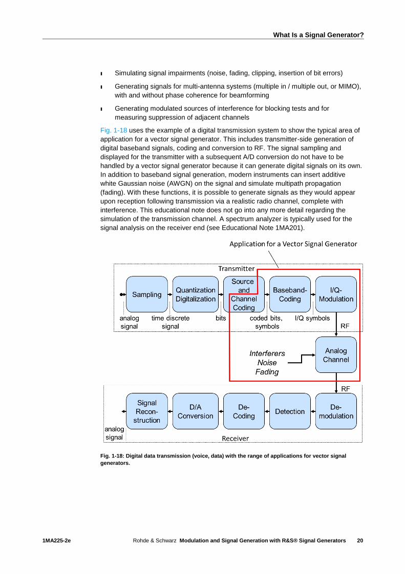
Fig. 1-18 uses the example of a digital transmission system to show the typical area of
application for a vector signal generator. This includes transmitter-side generation of
digital baseband signals, coding and conversion to RF. The signal sampling and
displayed for the transmitter with a subsequent A/D conversion do not have to be
handled by a vector signal generator because it can generate digital signals on its own.
In addition to baseband signal generation, modern instruments can insert additive
white Gaussian noise (AWGN) on the signal and simulate multipath propagation
(fading). With these functions, it is possible to generate signals as they would appear
upon reception following transmission via a realistic radio channel, complete with
interference. This educational note does not go into any more detail regarding the
simulation of the transmission channel. A spectrum analyzer is typically used for the
signal analysis on the receiver end (see Educational Note 1MA201).
Fig. 1-18: Digital data transmission (voice, data) with the range of applications for vector signal
generators.
What Is a Signal Generator?
1MA225-2e Rohde & Schwarz Modulation and Signal Generation with R&S® Signal Generators
21
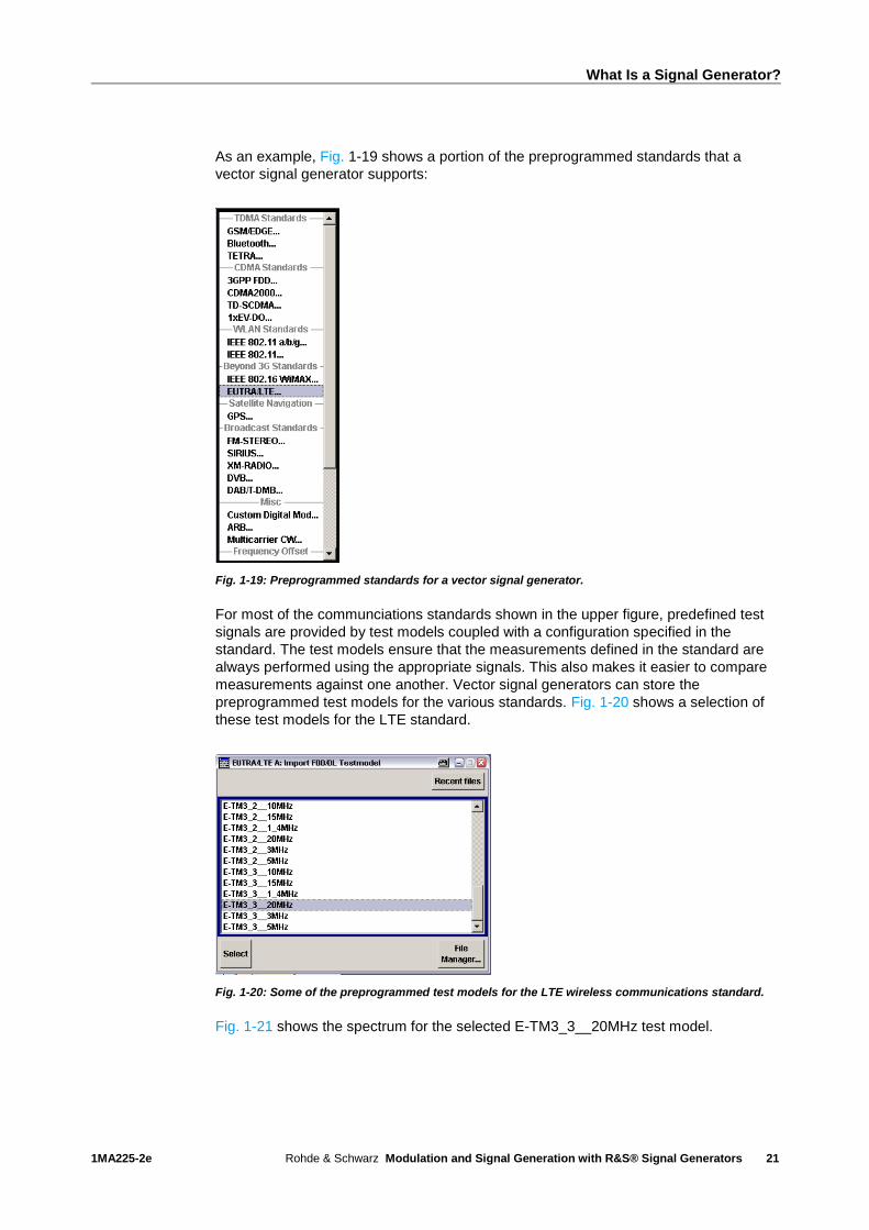
As an example, Fig. 1-19 shows a portion of the preprogrammed standards that a
vector signal generator supports:
Fig. 1-19: Preprogrammed standards for a vector signal generator.
For most of the communciations standards shown in the upper figure, predefined test
signals are provided by test models coupled with a configuration specified in the
standard. The test models ensure that the measurements defined in the standard are
always performed using the appropriate signals. This also makes it easier to compare
measurements against one another. Vector signal generators can store the
preprogrammed test models for the various standards. Fig. 1-20 shows a selection of
these test models for the LTE standard.
Fig. 1-20: Some of the preprogrammed test models for the LTE wireless communications standard.
Fig. 1-21 shows the spectrum for the selected E-TM3_3__20MHz test model.

What Is a Signal Generator?
1MA225-2e Rohde & Schwarz Modulation and Signal Generation with R&S® Signal Generators
22
Fig. 1-21: Multicarrier spectrum for the E-TM3_3__20MHz test model from the LTE standard.
The spectrum is approx. 18 MHz wide. A closer examination reveals that it consists of
1201 OFDM single carriers spaced 15 kHz apart, although they merge into each other
in this display due to the screen-resolution setting.
Fig. 1-22 shows the constellation diagram (I/Q display) for this test model.
Fig. 1-22: Overall constellation for the E-TM3_3__20MHz LTE test model.
The individual channels of this signal are modulated differently. All of the modulation
types being used are summarized in a single display:
BPSK (cyan), QPSK (red with blue crosses), 16 QAM (orange) and the constant
amplitude zero autocorrelation (CAZAC, blue) bits that are typical for LTE on the unit
circle.
In addition to the predefined test models and settings, today's vector signal generators
allow nearly all parameters of a digital standard to be modified. This makes it possible
to generate signals for almost any conceivable scenario that might be required for
specialized testing in development and production. For example, Fig. 1-23 shows the
input window for configuring an LTE frame.

What Is a Signal Generator?
1MA225-2e Rohde & Schwarz Modulation and Signal Generation with R&S® Signal Generators
23
Fig. 1-23: Configuration of an LTE frame.
Vector signal generators usually provide convenient triggering capabilities. This makes
it possible, for example, to fit generator bursts precisely into a prescribed time grid
(such as putting GSM bursts into the right time slots).
In parallel with the data stream, the generators generally also supply what are known
as marker signals at the device's jacks. These signals can be programmed for
activation at any position in the data stream (for example, at the beginning of a burst or
frame) in order to control a DUT or measuring instruments.
Unlike analog signals, digitally modulated signals sometimes have very high crest
factors. This means that the ratio between the average value and peak value can often
be more than 10 dB. Even small nonlinearities in the generator's amplifiers, mixers and
output stages can more readily cause harmonics and intermodulation products. In this
respect, there are considerable differences in the quality of individual generators.
Important characteristics for vector signal generators are the modulation bandwidth
and the achievable symbol rate, the modulation quality (error vector magnitude, EVM)
and the adjacent channel power (ACP) or adjacent channel leakage ratio (ACLR). For
more information, see section 1.3 Key Signal Generator Characteristics1.3. State-of-
the-art generators far exceed the requirements of the current mobile radio standards,
making them ready for the future. They also support a large number of international
standards.
As for analog generators, general criteria for selecting a vector signal generator include
the required output power, the settling time and accuracy for frequency and level, plus
a low reflection coefficient or VSWR. Additional considerations include low EVM
values, high dynamic range for ACP measurements and the number of supported
standards.
1.2.2.1 Design and functioning of a vector signal generator
The essential components of a vector signal generator are identical to that of an
analog generator. The synthesizer and output stage with ALC and step attenuator are
found here as well. As shown in Fig. 1-24, a baseband generator and an I-Q modulator
are used to generate the modulation (analog and digital) or to generate standard-
compliant mobile radio signals.

What Is a Signal Generator?
1MA225-2e Rohde & Schwarz Modulation and Signal Generation with R&S® Signal Generators
24
Fig. 1-24: Schematic of a vector signal generator.
Baseband generator
A vector signal generator produces modulated signals using I/Q modulation (see also
section 2.3). Often, an integrated baseband generator supplies in realtime the
modulation data that an I-Q modulator uses to modulate an RF carrier. Alternatively, a
vector signal generator can be supplied with the complex modulation signals and a
universal analog I and Q input via an external true baseband generator. Although
digital supply is also common, only proprietary inputs are available because no
industry-wide standard has been agreed upon for digital modulation using signal
generators.
What Is a Signal Generator?
1MA225-2e Rohde & Schwarz Modulation and Signal Generation with R&S® Signal Generators
25
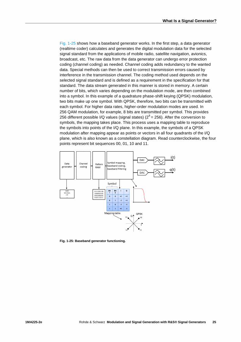
Fig. 1-25 shows how a baseband generator works. In the first step, a data generator
(realtime coder) calculates and generates the digital modulation data for the selected
signal standard from the applications of mobile radio, satellite navigation, avionics,
broadcast, etc. The raw data from the data generator can undergo error protection
coding (channel coding) as needed. Channel coding adds redundancy to the wanted
data. Special methods can then be used to correct transmission errors caused by
interference in the transmission channel. The coding method used depends on the
selected signal standard and is defined as a requirement in the specification for that
standard. The data stream generated in this manner is stored in memory. A certain
number of bits, which varies depending on the modulation mode, are then combined
into a symbol. In this example of a quadrature phase-shift keying (QPSK) modulation,
two bits make up one symbol. With QPSK, therefore, two bits can be transmitted with
each symbol. For higher data rates, higher-order modulation modes are used. In
256 QAM modulation, for example, 8 bits are transmitted per symbol. This provides
256 different possible I/Q values (signal states) (28 = 256). After the conversion to
symbols, the mapping takes place. This process uses a mapping table to reproduce
the symbols into points of the I/Q plane. In this example, the symbols of a QPSK
modulation after mapping appear as points or vectors in all four quadrants of the I/Q
plane, which is also known as a constellation diagram. Read counterclockwise, the four
points represent bit sequences 00, 01, 10 and 11.
Fig. 1-25: Baseband generator functioning.
What Is a Signal Generator?
1MA225-2e Rohde & Schwarz Modulation and Signal Generation with R&S® Signal Generators
26
Fig. 1-26 shows the data streams i(t) and q(t) after the mapping of a QPSK-modulated
signal and the derived vector position.
Fig. 1-26: Time characteristic of i(t) and q(t) for QPSK.
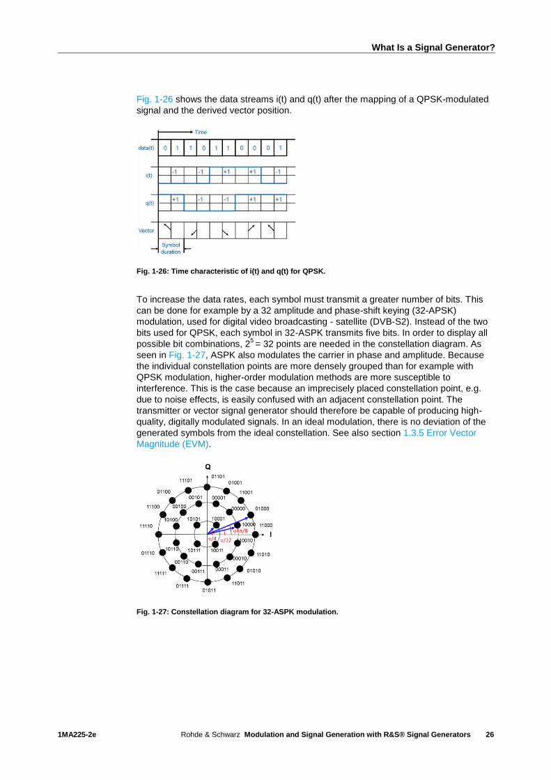
To increase the data rates, each symbol must transmit a greater number of bits. This
can be done for example by a 32 amplitude and phase-shift keying (32-APSK)
modulation, used for digital video broadcasting - satellite (DVB-S2). Instead of the two
bits used for QPSK, each symbol in 32-ASPK transmits five bits. In order to display all
possible bit combinations, 25 = 32 points are needed in the constellation diagram. As
seen in Fig. 1-27, ASPK also modulates the carrier in phase and amplitude. Because
the individual constellation points are more densely grouped than for example with
QPSK modulation, higher-order modulation methods are more susceptible to
interference. This is the case because an imprecisely placed constellation point, e.g.
due to noise effects, is easily confused with an adjacent constellation point. The
transmitter or vector signal generator should therefore be capable of producing high-
quality, digitally modulated signals. In an ideal modulation, there is no deviation of the
generated symbols from the ideal constellation. See also section 1.3.5 Error Vector
Magnitude (EVM).
Fig. 1-27: Constellation diagram for 32-ASPK modulation.
What Is a Signal Generator?
1MA225-2e Rohde & Schwarz Modulation and Signal Generation with R&S® Signal Generators
27
In the case of a digital modulation, certain symbol sequences can result in extreme
jumps between two points in the constellation diagram. For example, a change in the
symbol from 11001 to 11111 (Fig. 1-27) will cause a transition from maximum
amplitude – zero crossing – maximum amplitude; amplification of these types of
signals requires a great deal of effort as a result of the high crest factor. To prevent
these zero crossings, special modulation modes such as π/4-DQPSK are used (see
section 2.4.3). To prevent high crest factors (ratio of peak value to RMS value, see
section 2.4.6 ), a baseband coding also takes place in the baseband. With a suitable
coding, this should prevent small amplitude jumps without zero crossings at a symbol
transition (Fig. 1-28).
Fig. 1-28: Preventing large amplitude jumps through the use of a π/4-DQPSK modulation.
In the time domain, the data streams from Fig. 1-26 represent square-wave pulse sequences with pulse duration ∆t and a pulse period duration T. In the frequency
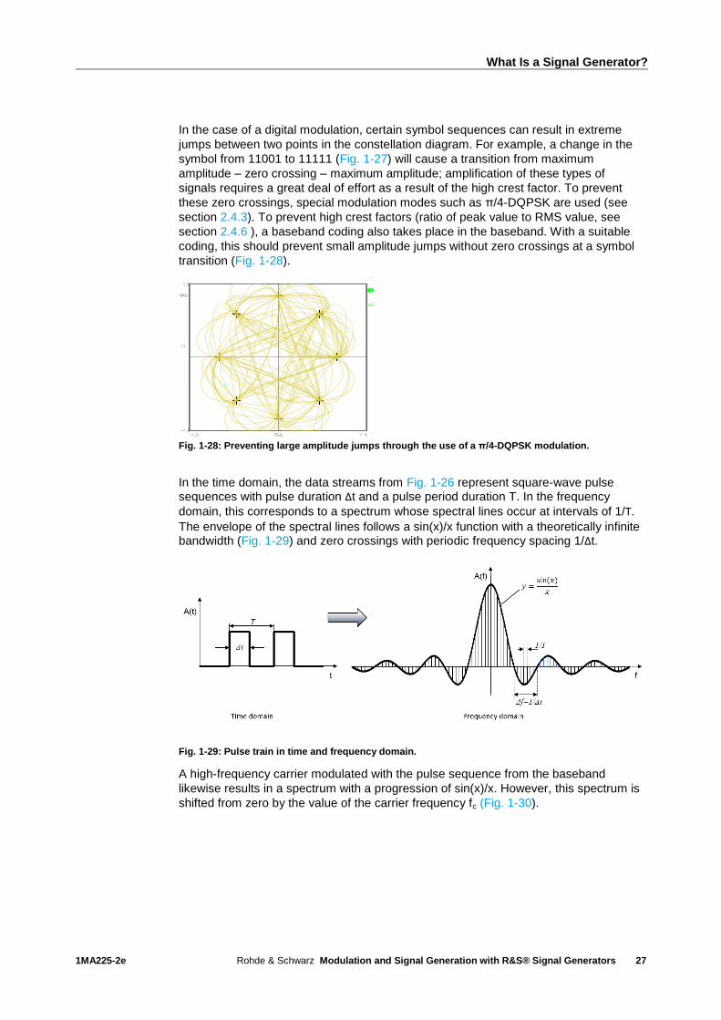
domain, this corresponds to a spectrum whose spectral lines occur at intervals of 1/T.
The envelope of the spectral lines follows a sin(x)/x function with a theoretically infinite bandwidth (Fig. 1-29) and zero crossings with periodic frequency spacing 1/∆t.
Fig. 1-29: Pulse train in time and frequency domain.
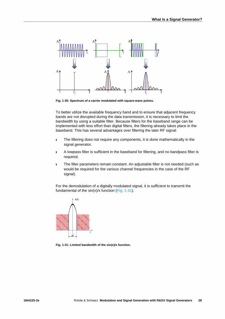
A high-frequency carrier modulated with the pulse sequence from the baseband
likewise results in a spectrum with a progression of sin(x)/x. However, this spectrum is
shifted from zero by the value of the carrier frequency fc (Fig. 1-30).
What Is a Signal Generator?
1MA225-2e Rohde & Schwarz Modulation and Signal Generation with R&S® Signal Generators
28
Fig. 1-30: Spectrum of a carrier modulated with square-wave pulses.
To better utilize the available frequency band and to ensure that adjacent frequency
bands are not disrupted during the data transmission, it is necessary to limit the
bandwidth by using a suitable filter. Because filters for the baseband range can be
implemented with less effort than digital filters, the filtering already takes place in the
baseband. This has several advantages over filtering the later RF signal:
ı The filtering does not require any components, it is done mathematically in the
signal generator.
ı A lowpass filter is sufficient in the baseband for filtering, and no bandpass filter is
required.
ı The filter parameters remain constant. An adjustable filter is not needed (such as
would be required for the various channel frequencies in the case of the RF
signal).
For the demodulation of a digitally modulated signal, it is sufficient to transmit the
fundamental of the sin(x)/x function (Fig. 1-31).
Fig. 1-31: Limited bandwidth of the sin(x)/x function.
What Is a Signal Generator?
1MA225-2e Rohde & Schwarz Modulation and Signal Generation with R&S® Signal Generators
29
In practice, however, the filtering is not performed using a square-wave filter as shown
in Fig. 1-31. Square-wave filters (also called ideal lowpass filters) lead to strong,
disruptive signal overshoots in the time domain (Fig. 1-30). This makes it impossible to
correctly distinguish the individual bits in a bit sequence. To prevent this, filters with
special filter characteristics or special edge shapes are used. Examples include raised
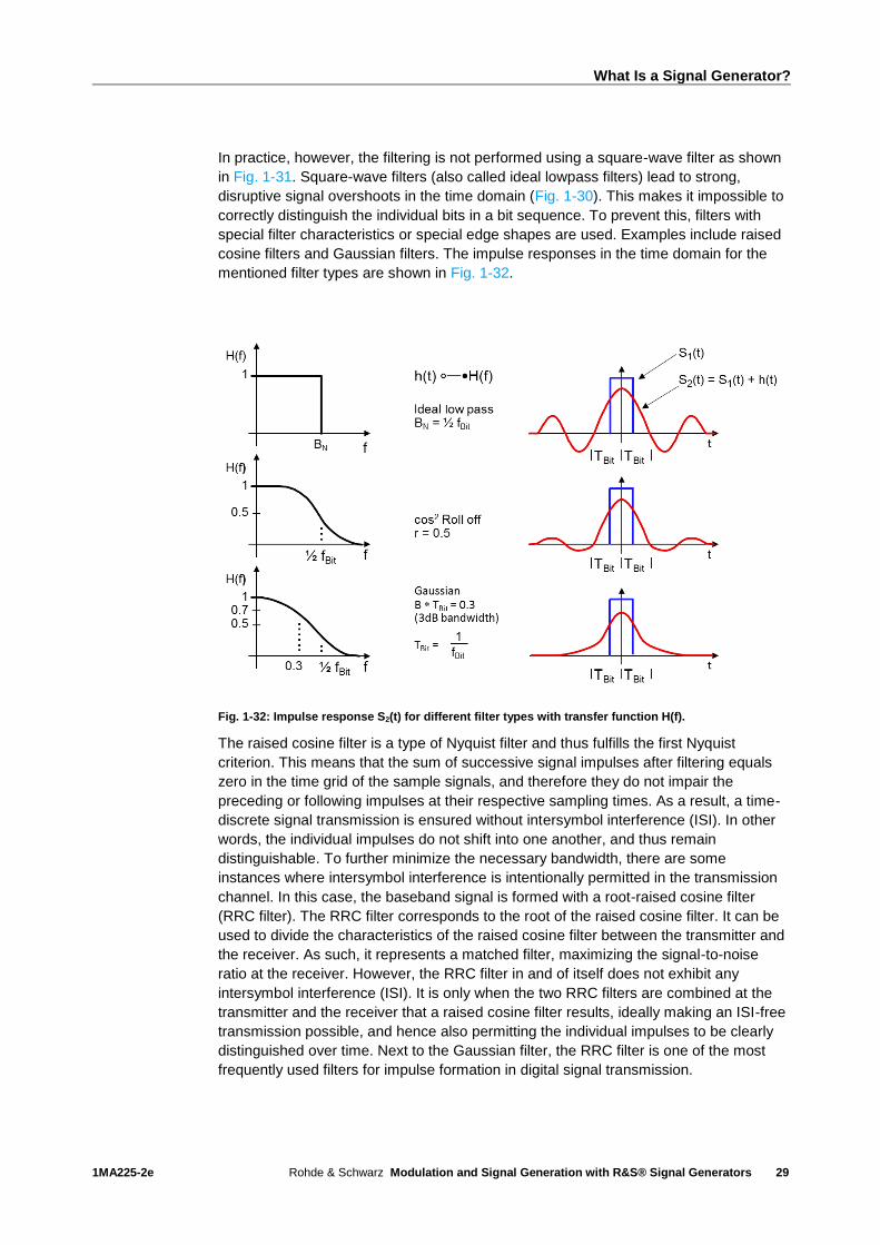
cosine filters and Gaussian filters. The impulse responses in the time domain for the
mentioned filter types are shown in Fig. 1-32.
Fig. 1-32: Impulse response S2(t) for different filter types with transfer function H(f).
The raised cosine filter is a type of Nyquist filter and thus fulfills the first Nyquist
criterion. This means that the sum of successive signal impulses after filtering equals
zero in the time grid of the sample signals, and therefore they do not impair the
preceding or following impulses at their respective sampling times. As a result, a time-
discrete signal transmission is ensured without intersymbol interference (ISI). In other
words, the individual impulses do not shift into one another, and thus remain
distinguishable. To further minimize the necessary bandwidth, there are some
instances where intersymbol interference is intentionally permitted in the transmission
channel. In this case, the baseband signal is formed with a root-raised cosine filter
(RRC filter). The RRC filter corresponds to the root of the raised cosine filter. It can be
used to divide the characteristics of the raised cosine filter between the transmitter and
the receiver. As such, it represents a matched filter, maximizing the signal-to-noise
ratio at the receiver. However, the RRC filter in and of itself does not exhibit any
intersymbol interference (ISI). It is only when the two RRC filters are combined at the
transmitter and the receiver that a raised cosine filter results, ideally making an ISI-free
transmission possible, and hence also permitting the individual impulses to be clearly
distinguished over time. Next to the Gaussian filter, the RRC filter is one of the most
frequently used filters for impulse formation in digital signal transmission.

What Is a Signal Generator?
1MA225-2e Rohde & Schwarz Modulation and Signal Generation with R&S® Signal Generators
30
The transfer function of the raised cosine filter and the RRC filter is dependent on both the symbol rate (1/T) and the rolloff factor r. Fig. 1-33 shows the transfer function of the above-mentioned filters and the derived rolloff factor. The rolloff factor can be a value between 0 and 1 and influences the steepness of the transmission curve.
Fig. 1-33: Rolloff factor definition.
Fig. 1-34 shows the transfer function H(f) and time function h(t) of a raised cosine filter
with four different rolloff factors. Where r = 0, the result is an ideal lowpass with a
square-wave transfer function, while r = 1 delivers the flattest possible cosine edge.
Where r is an intermediate value, the frequency response is close to constant over a
certain range, then falls into a somewhat steeper cosine edge as the values for r
decrease. The filter bandwidth increases as the rolloff factor increases. The maximum
value of r = 1 is equal to the maximum bandwidth of 1/T. A decreasing rolloff factor
produces a steeper filter edge and leads to greater undesirable overshoots in the time
domain. In practice, however, a smaller rolloff factor in the range from 0.2 to 0.5 will
save bandwidth. For example, the UMTS mobile cellular standard uses a rolloff factor
of r = 0.22 for its impulse filter.
Fig. 1-34: Transfer function H(f) and time function h(t) of a raised cosine filter with various rolloff
factors.
What Is a Signal Generator?
1MA225-2e Rohde & Schwarz Modulation and Signal Generation with R&S® Signal Generators
31
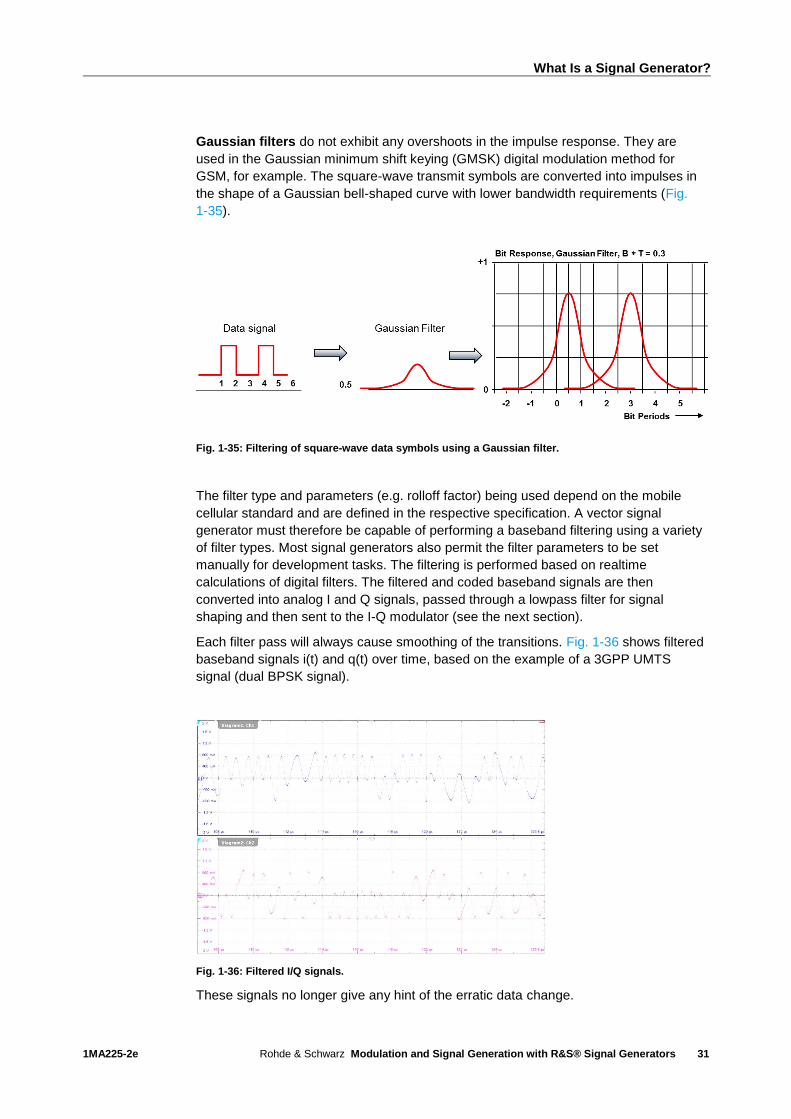
Gaussian filters do not exhibit any overshoots in the impulse response. They are
used in the Gaussian minimum shift keying (GMSK) digital modulation method for
GSM, for example. The square-wave transmit symbols are converted into impulses in
the shape of a Gaussian bell-shaped curve with lower bandwidth requirements (Fig.
1-35).
Fig. 1-35: Filtering of square-wave data symbols using a Gaussian filter.
The filter type and parameters (e.g. rolloff factor) being used depend on the mobile
cellular standard and are defined in the respective specification. A vector signal
generator must therefore be capable of performing a baseband filtering using a variety
of filter types. Most signal generators also permit the filter parameters to be set
manually for development tasks. The filtering is performed based on realtime
calculations of digital filters. The filtered and coded baseband signals are then
converted into analog I and Q signals, passed through a lowpass filter for signal
shaping and then sent to the I-Q modulator (see the next section).
Each filter pass will always cause smoothing of the transitions. Fig. 1-36 shows filtered
baseband signals i(t) and q(t) over time, based on the example of a 3GPP UMTS
signal (dual BPSK signal).
Fig. 1-36: Filtered I/Q signals.
These signals no longer give any hint of the erratic data change.
What Is a Signal Generator?
1MA225-2e Rohde & Schwarz Modulation and Signal Generation with R&S® Signal Generators
32
At the left of Fig. 1-37 is the position of an I/Q constellation relative to the symbol times
and to the right is the I/Q vector over time. As a result of filtering, this no longer follows
the shortest straight line between the symbols, but rather describes the filtering
characteristics of the symbol transitions.
Fig. 1-37: Constellation (left) and continuous vector display.
I-Q modulator
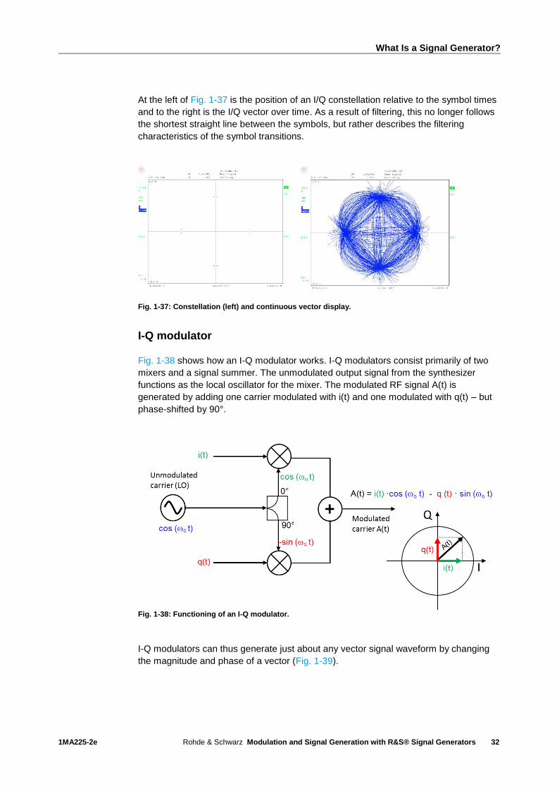
Fig. 1-38 shows how an I-Q modulator works. I-Q modulators consist primarily of two
mixers and a signal summer. The unmodulated output signal from the synthesizer
functions as the local oscillator for the mixer. The modulated RF signal A(t) is
generated by adding one carrier modulated with i(t) and one modulated with q(t) – but
phase-shifted by 90°.
Fig. 1-38: Functioning of an I-Q modulator.
I-Q modulators can thus generate just about any vector signal waveform by changing
the magnitude and phase of a vector (Fig. 1-39).

What Is a Signal Generator?
1MA225-2e Rohde & Schwarz Modulation and Signal Generation with R&S® Signal Generators
33
Fig. 1-39: Using an I-Q modulator to generate a signal from the I and Q signal.
For even more flexibility during signal generation, some signal generators can
optionally also include an arbitrary waveform generator (ARB) as the baseband signal
source (see also section 1.2.3). This generates signals of almost unlimited complexity.
The disadvantage is that the signal generation cannot be performed in realtime and a
precalculated signal waveform must be available, for example created using PC
software or a mathematical software application.
1.2.3 Arbitrary Waveform Generators (ARBs)
Arbitrary waveform generators (ARBs) are specialized vector signal generators for the
baseband. The modulation data for ARBs is calculated in advance (rather than in
realtime) and stored in the instrument's RAM. The memory content is then output at the
realtime symbol rate. Many vector signal generators have an ARB option; see selection
in Fig. 1-19. ARBs differ from realtime vector generators in use and application as
listed here:
ı ARBs have zero restrictions for configuring the content of an I/Q data stream
(hence the name "arbitrary").
ı Only time-limited or cyclic signals are allowed (the memory depth is finite).
The memory depth and word width for the I/Q data sets are additional characteristics
for ARBs. Some ARB generators allow sequential playback of different memory
segments containing multiple precalculated waveforms, without any further preliminary
calculation.
As with realtime generators, ARBs offer different triggering options as well as the ability
to output marker signals for controlling connected hardware and measurement
instruments in parallel to the waveform playback. Users can combine a variety of
waveforms of varying durations into a single sequence for production tests (see Fig.
1-40). The sequence and duration is defined either in the ARB by means of a remote
control program or by using an external trigger signal. For example, the output
sequence can consist of data streams with varying bit rates that must be verified during
production.
What Is a Signal Generator?
1MA225-2e Rohde & Schwarz Modulation and Signal Generation with R&S® Signal Generators
34
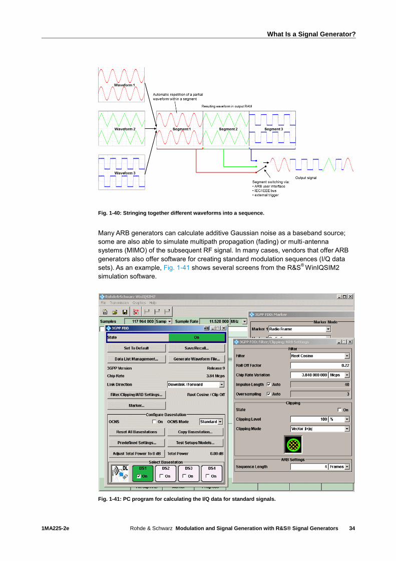
Fig. 1-40: Stringing together different waveforms into a sequence.
Many ARB generators can calculate additive Gaussian noise as a baseband source;
some are also able to simulate multipath propagation (fading) or multi-antenna
systems (MIMO) of the subsequent RF signal. In many cases, vendors that offer ARB
generators also offer software for creating standard modulation sequences (I/Q data
sets). As an example, Fig. 1-41 shows several screens from the R&S®
WinIQSIM2
simulation software.
Fig. 1-41: PC program for calculating the I/Q data for standard signals.

What Is a Signal Generator?
1MA225-2e Rohde & Schwarz Modulation and Signal Generation with R&S® Signal Generators
35
This example uses the 3GPP FDD (UMTS) mobile cellular standard. It illustrates the
creation of a downlink, i.e. the signal from a base station (BS) to a mobile phone. The
program can generate the signals from up to four base stations; in Fig. 1-41, only BS1
is active. The filtering complies with the UMTS standard. No clipping is performed. The
Marker1 device jack will subsequently deliver a signal with each new radio frame.
Once all the required entries have been made, the user initiates calculation of the I/Q
data by clicking the Generate Waveform File button. The data is then transferred from
the program to the ARB, and the output can be started immediately.
Fig. 1-42 shows the basic functioning of an ARB. The sequencer takes the waveforms
saved in memory and combines them into a predefined sequence, then forwards them
to the sample rate converter (resampler).
The resampler is used to adjust a variable memory symbol clock to a fixed clock rate
from the D/A converter. This has two major advantages. First, the D/A converter
always uses the optimal clock rate for the best possible resolution, and second, the
variable memory clock ensures that the memory is optimally utilized. In other words,
changing the clock ensures that the longest possible sequence can be generated.
This is illustrated in the following example:
An ARB with a memory depth of 1 Gsample can generate a GSM signal with
270 ksamples/s and triple oversampling with a duration of 1234 s.
(𝑡 = 1 𝐺𝑠𝑎𝑚𝑝𝑙𝑒
3∙270 𝑘𝑠𝑎𝑚𝑝𝑙𝑒). If the memory clock rate is equal to that of the D/A converter, for
example 300 MHz, the possible duration for the signal output would be reduced to
3.3 s (𝑡 = 1 𝐺𝑠𝑎𝑚𝑝𝑙𝑒
300 𝑀𝑠𝑎𝑚𝑝𝑙𝑒/𝑠).
Because the clock rate of the D/A converter is always within the optimal range, the
output signal has a high, spurious-free dynamic range (SFDR) that is independent of
the memory clock rate.
Fig. 1-42: ARB block diagram.

What Is a Signal Generator?
1MA225-2e Rohde & Schwarz Modulation and Signal Generation with R&S® Signal Generators
36
1.3 Key Signal Generator Characteristics
An ideal assumed signal generator delivers an undistorted sine-wave signal that
exactly matches the defined frequency and the defined level at its output. Fig. 1-43
shows an ideal sine-wave signal in the time and frequency domains.
Fig. 1-43: Output signal of an ideal signal generator in the time and frequency domains.
Because a signal generator is constructed from real components with non-ideal
characteristics, the wanted carrier signal with frequency fc (c: carrier) arrives at the
output along with other, unwanted signals. In reality, even the carrier signal will include
a level error and a frequency error. In fact, as a result of the phase noise, the real
carrier signal is not consistently displayed in the spectrum as a thin line, or Dirac pulse
(see Fig. 1-44).
Fig. 1-44: Real spectrum for a non-ideal signal generator.
The following sections take a closer look at the key signal generator characteristics
used to assess signal quality.
1.3.1 Phase Noise
Phase noise is a measure of the short-term stability of oscillators as used in a signal
generator for producing signals of varying frequency and shape. Phase noise is
caused by fluctuations in phase, frequency and amplitudes of an oscillator output

What Is a Signal Generator?
1MA225-2e Rohde & Schwarz Modulation and Signal Generation with R&S® Signal Generators
37
signal, although the latter are usually not a consideration. These fluctuations have a
modulating effect. Phase noise typically occurs symmetrically around the carrier, which
is why it is sufficient to consider only the phase noise on one side of the carrier. Its
amplitude is therefore specified as single sideband phase noise (SSB) at a defined
carrier offset referenced to the carrier amplitude. The specified values are usually
relative, i.e. they are defined as a noise power level within a bandwidth of 1 Hz.
Accordingly, the unit is noted as dBc (1 Hz) or as dBc/Hz, where "c" references the
carrier. Because the phase noise power is lower than the carrier power, negative
values are to be expected in the specifications for a signal generator. The effects of
phase noise are shown in Fig. 1-45.
Fig. 1-45: Phase noise of an OCXO, a VCO and a VCO connected to the OCXO at varying PLL
bandwidths.
Ideally, a pure sine-wave signal would result in a single spectral line in the frequency
domain. In practice, however, the spectrum of a signal generated by a real oscillator is
significantly broader. Signals from all oscillators exhibit phase noise to some degree.
By making appropriate changes to the circuitry, this can be minimized to a certain
extent, but never completely eliminated. In modern signal generators, oscillators are
implemented as synthesizers, i.e. the actual oscillators are locked to a highly precise
reference frequency, e.g. 10 MHz, by phase-locked loops as described in 1.2.1.1. The
phase noise characteristics are affected by the PLL bandwidth of the frequency locking
circuitry. The following subranges can therefore be identified (see also ranges 1, 2 and
3 in Fig. 1-45):
ı Close to the carrier (frequency offset up to about 1 kHz)
In this range, the phase noise caused by the multiplication in the locked loop is
higher than that from the reference oscillator.
ı Range extending to the upper boundary of the PLL bandwidth (starting at about
1 kHz)
What Is a Signal Generator?
1MA225-2e Rohde & Schwarz Modulation and Signal Generation with R&S® Signal Generators
38
Within the PLL bandwidth, the phase noise corresponds to the total noise from
multiple components in the locked loop, including the attenuator, the phase
detector and the multiplexed reference signal. The upper boundary of this range is
dependent on the signal generator, or more accurately, on the type of oscillator
used.
ı Range outside of the control bandwidth
Outside of the control bandwidth, the phase noise is determined almost entirely by
the phase noise of the oscillator during unsynchronized operation. In this range, it
falls 20 dB per decade.
Fig. 1-45 shows the phase noise for the various PLL bandwidths. Of interest is the
comparison of the phase noise from the unsynchronized oscillator against the phase
noise using the various PLL bandwidths as reference. The following different situations
can occur:
ı Large PLL bandwidth
The loop gain in the locked loop is so high that the noise from the oscillator
connected to the reference is reduced to the level of the noise from the reference.
Far away from the carrier, however, the phase noise increases as a result of the
phase shift caused by the filtering.
ı Medium PLL bandwidth
The loop gain is not sufficient to reach the reference noise close to the carrier.
However, the increase in phase noise far away from the carrier is less than with a
large control bandwidth.
ı Narrow PLL bandwidth
The phase noise far away from the carrier is not any worse than that from the
unsynchronized oscillator. Close to the carrier however, it is significantly greater
compared to the medium and large control bandwidths.
Mathematical description of phase noise:
The output signal v(t) of an ideal oscillator can be described by
Equation 1-3:
v(t) = Vo · sin(2πfo t) where
Vo Signal amplitude
F0 Signal frequency and
2πfo t Signal phase
With real signals, both the signal's amplitude and its phase are subject to fluctuations:
Equation 1-4:
v(t) = (Vo + )(t ) sin(2πfo + )(t ) where

What Is a Signal Generator?
1MA225-2e Rohde & Schwarz Modulation and Signal Generation with R&S® Signal Generators
39
)(t The signal's amplitude variation and
)(t The signal's (phase variation or) phase noise
When working with the term )(t , it is necessary to differentiate between two types:
ı Deterministic phase fluctuation due to e.g. AC hum or to insufficient suppression
of other frequencies during signal processing. These fluctuations appear as
discrete lines of interference.
ı Random phase fluctuations caused by thermal, shot or flicker noise in the active
elements of oscillators.
One measure of phase noise is the noise power density referenced to 1 Hertz of
bandwidth:
Equation 1-5:
Hz
rad
Hz1)(
2rms
2
fS
In practice, single sideband (SSB) phase noise L is usually used to describe an
oscillator's phase-noise characteristics. It is defined as the ratio of the noise power
measured in a single sideband SSBP at 1 Hz of bandwidth) to the signal power CarrierP
at a frequency offset offsetf from the carrier (see also Fig. 1-46).
Equation 1-6:
Carrier
SSB Hz1)(
P
PfL offset
Fig. 1-46: Ideal signal and signal with phase noise.

What Is a Signal Generator?
1MA225-2e Rohde & Schwarz Modulation and Signal Generation with R&S® Signal Generators
40
If the modulation sidebands are very small due to noise, i.e. if the phase deviation is
much smaller than 1 rad, the SSB phase noise can be derived from the noise power
density:
Equation 1-7:
)(2
1)( fSfL
The SSB phase noise is commonly specified on a logarithmic scale:
Equation 1-8:
dBc))((lg10)( offsetoffsetc fLfL
The SSB phase noise from a signal generator based on the frequency offset to the
carrier is shown in Fig. 1-47. Because the components used for signal generation
possess frequency-dependent characteristics, and because the higher frequencies
require additional signal paths for the signal generation, the phase noise is also
dependent on the frequency currently defined for the signal generator. Fig. 1-47 shows
this dependency for several carrier frequencies ranging from 10 MHz to 6 GHz. This
illustrates that phase noise increases almost continuously in relationship to the
frequency.
Fig. 1-47: SSB phase noise based on the frequency offset at various carrier frequencies.
Low phase noise values as seen in Fig. 1-47 are particularly significant when a signal
generator will be used as a stable reference signal, for example for phase noise
measurements, or as a calibration reference during servicing. Low-jitter microwave

What Is a Signal Generator?
1MA225-2e Rohde & Schwarz Modulation and Signal Generation with R&S® Signal Generators
41
signals, i.e. signals with low SSB phase noise – in particular close to the carrier – are
essential for characterizing ever-faster A/D converters.
1.3.2 Spurious Emissions
The spurious emissions shown in Fig. 1-44 (harmonics and subharmonics) are the
result of non-linearities in the components (amplifiers, mixers, etc.) in the signal path of
the signal generator. This is described in more detail below.
An ideal linear two-port device transfers signals from the input to the output without
distorting them. The voltage transfer function of this type of two-port device is:
Equation 1-9:
Vout(t) = GV · Vin(t)
where Vout(t): Voltage at the output of the two-port device
Vin(t): Voltage at the input of the two-port device
GV: Voltage gain in the two-port device
In practice, these types of ideal two-port devices can be achieved only by using
passive components.
For example, resistive attenuators can be assumed to be ideal. On the other hand,
two-port devices containing semiconductor components, e.g. amplifiers or mixers, do
exhibit non-linearities. In this case, the transfer function can be approximated by using
a power series. The following applies:
Equation 1-10:
v𝑜𝑢𝑡(t) = ∑ 𝑎𝑛 ∙ v𝑖𝑛𝑛 (𝑡) =
∞
𝑛=1
𝑎1 ∙ v𝑖𝑛(𝑡) + 𝑎2 ∙ v𝑖𝑛2 (𝑡) + 𝑎3 ∙ v𝑖𝑛
3 (𝑡)+. ..
where vout(t): Voltage at the output of the two-port device
vin(t): Voltage at the input of the two-port device
an: Coefficient of the respective non-linear element for the voltage
gain
In most cases, it is sufficient to consider the square and cubic members, so that the
power series need only be developed up to n = 3 as shown in Equation 1-10. Signal
generators should deliver the most distortion-free signals possible. Linearity is
therefore a key criterion for assessing a signal generator. The effects of a two-port
device's non-linearities on its output spectrum are dependent on the input signal:
Single-tone modulation
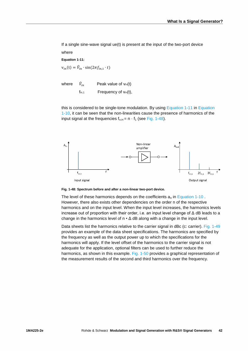
What Is a Signal Generator?
1MA225-2e Rohde & Schwarz Modulation and Signal Generation with R&S® Signal Generators
42
If a single sine-wave signal ue(t) is present at the input of the two-port device
where
Equation 1-11:
v𝑖𝑛(t) = 𝑖𝑛 ∙ sin(2𝜋𝑓𝑖𝑛,1 ∙ 𝑡)
where 𝑖𝑛 Peak value of vin(t)
fin,1 Frequency of vin(t),
this is considered to be single-tone modulation. By using Equation 1-11 in Equation
1-10, it can be seen that the non-linearities cause the presence of harmonics of the
input signal at the frequencies fn.H = n · f1 (see Fig. 1-48).
Fig. 1-48: Spectrum before and after a non-linear two-port device.
The level of these harmonics depends on the coefficients an in Equation 1-10 .
However, there also exists other dependencies on the order n of the respective
harmonics and on the input level. When the input level increases, the harmonics levels
increase out of proportion with their order, i.e. an input level change of Δ dB leads to a
change in the harmonics level of n • Δ dB along with a change in the input level.
Data sheets list the harmonics relative to the carrier signal in dBc (c: carrier). Fig. 1-49
provides an example of the data sheet specifications. The harmonics are specified by
the frequency as well as the output power up to which the specifications for the
harmonics will apply. If the level offset of the harmonics to the carrier signal is not
adequate for the application, optional filters can be used to further reduce the
harmonics, as shown in this example. Fig. 1-50 provides a graphical representation of
the measurement results of the second and third harmonics over the frequency.

What Is a Signal Generator?
1MA225-2e Rohde & Schwarz Modulation and Signal Generation with R&S® Signal Generators
43
Fig. 1-49: Example specifications for harmonics.
Fig. 1-50: Graphical display of the second and third harmonics up to 6 GHz, output power +15 dBm
(measured).
Two-tone modulation
In addition to the harmonics described above, the signal generation also results in non-
harmonic signal components. Because the isolation of the signal paths is limited, these
components can be caused by crosstalk from internal power supplies or from other
clock frequencies present in the signal generator, for example. This includes
intermodulation products such as those that occur during two-tone modulation of non-
linear components. In the case of two-tone modulation, a signal Vin(t) consisting of two
sine-wave signals of the same amplitude is applied at the input of the two-port device.
The following applies for the input signal:
Equation 1-12:
v𝑖𝑛(t) = 𝑖𝑛 ∙ sin(2𝜋𝑓𝑖𝑛,1 ∙ 𝑡) + 𝑖𝑛 ∙ sin(2𝜋𝑓𝑖𝑛,2 ∙ 𝑡)
where 𝑖𝑛 Peak value of the two sine-wave signals
fin,1, fin,2 Signal frequencies
By using Equation 1-12 in the non-linear transfer function per Equation 1-10, the
intermodulation products listed in Table 1-1 are present at the output of the two-port
device. The angular frequency ω is always specified with ω1 = 2π · fin,1 and
ω2 = 2 π · fin,2.
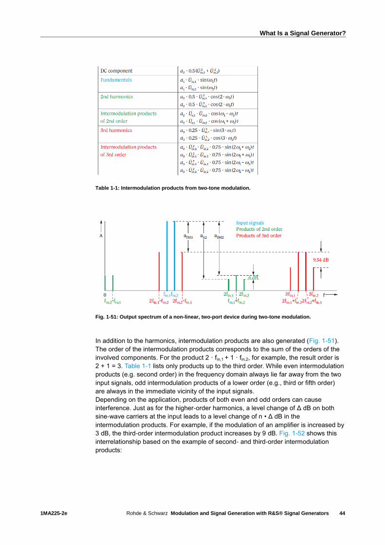
What Is a Signal Generator?
1MA225-2e Rohde & Schwarz Modulation and Signal Generation with R&S® Signal Generators
44
Table 1-1: Intermodulation products from two-tone modulation.
Fig. 1-51: Output spectrum of a non-linear, two-port device during two-tone modulation.
In addition to the harmonics, intermodulation products are also generated (Fig. 1-51).
The order of the intermodulation products corresponds to the sum of the orders of the
involved components. For the product 2 · fin,1 + 1 · fin,2, for example, the result order is
2 + 1 = 3. Table 1-1 lists only products up to the third order. While even intermodulation
products (e.g. second order) in the frequency domain always lie far away from the two
input signals, odd intermodulation products of a lower order (e.g., third or fifth order)
are always in the immediate vicinity of the input signals.
Depending on the application, products of both even and odd orders can cause
interference. Just as for the higher-order harmonics, a level change of Δ dB on both
sine-wave carriers at the input leads to a level change of n • Δ dB in the
intermodulation products. For example, if the modulation of an amplifier is increased by
3 dB, the third-order intermodulation product increases by 9 dB. Fig. 1-52 shows this
interrelationship based on the example of second- and third-order intermodulation
products:
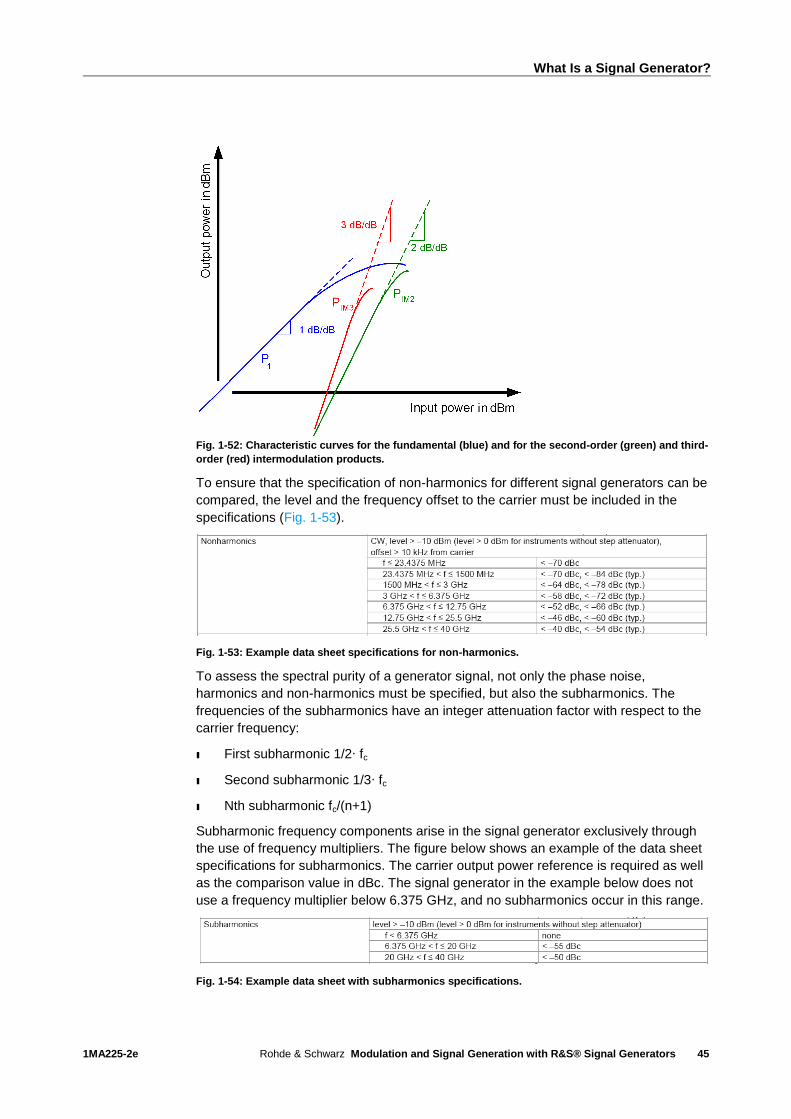
What Is a Signal Generator?
1MA225-2e Rohde & Schwarz Modulation and Signal Generation with R&S® Signal Generators
45
Fig. 1-52: Characteristic curves for the fundamental (blue) and for the second-order (green) and third-
order (red) intermodulation products.
To ensure that the specification of non-harmonics for different signal generators can be
compared, the level and the frequency offset to the carrier must be included in the
specifications (Fig. 1-53).
Fig. 1-53: Example data sheet specifications for non-harmonics.
To assess the spectral purity of a generator signal, not only the phase noise,
harmonics and non-harmonics must be specified, but also the subharmonics. The
frequencies of the subharmonics have an integer attenuation factor with respect to the
carrier frequency:
ı First subharmonic 1/2∙ fc
ı Second subharmonic 1/3∙ fc
ı Nth subharmonic fc/(n+1)
Subharmonic frequency components arise in the signal generator exclusively through
the use of frequency multipliers. The figure below shows an example of the data sheet
specifications for subharmonics. The carrier output power reference is required as well
as the comparison value in dBc. The signal generator in the example below does not
use a frequency multiplier below 6.375 GHz, and no subharmonics occur in this range.
Fig. 1-54: Example data sheet with subharmonics specifications.
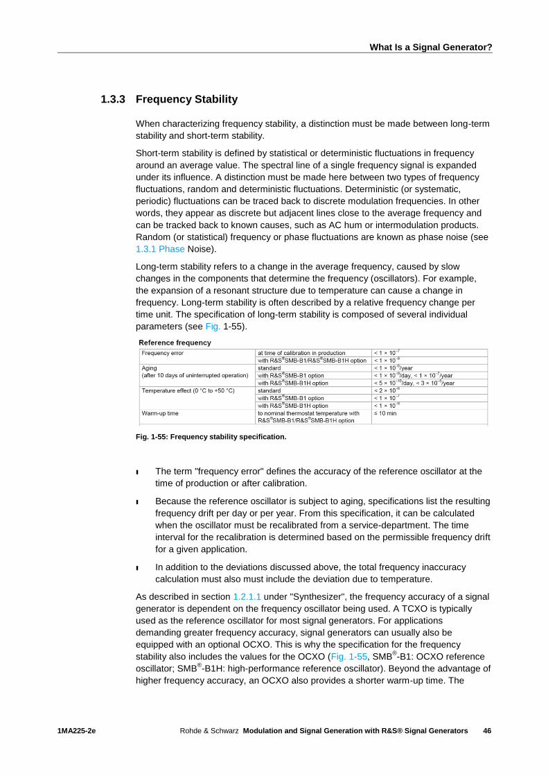
What Is a Signal Generator?
1MA225-2e Rohde & Schwarz Modulation and Signal Generation with R&S® Signal Generators
46
1.3.3 Frequency Stability
When characterizing frequency stability, a distinction must be made between long-term
stability and short-term stability.
Short-term stability is defined by statistical or deterministic fluctuations in frequency
around an average value. The spectral line of a single frequency signal is expanded
under its influence. A distinction must be made here between two types of frequency
fluctuations, random and deterministic fluctuations. Deterministic (or systematic,
periodic) fluctuations can be traced back to discrete modulation frequencies. In other
words, they appear as discrete but adjacent lines close to the average frequency and
can be tracked back to known causes, such as AC hum or intermodulation products.
Random (or statistical) frequency or phase fluctuations are known as phase noise (see
1.3.1 Phase Noise).
Long-term stability refers to a change in the average frequency, caused by slow
changes in the components that determine the frequency (oscillators). For example,
the expansion of a resonant structure due to temperature can cause a change in
frequency. Long-term stability is often described by a relative frequency change per
time unit. The specification of long-term stability is composed of several individual
parameters (see Fig. 1-55).
Fig. 1-55: Frequency stability specification.
ı The term "frequency error" defines the accuracy of the reference oscillator at the
time of production or after calibration.
ı Because the reference oscillator is subject to aging, specifications list the resulting
frequency drift per day or per year. From this specification, it can be calculated
when the oscillator must be recalibrated from a service-department. The time
interval for the recalibration is determined based on the permissible frequency drift
for a given application.
ı In addition to the deviations discussed above, the total frequency inaccuracy
calculation must also must include the deviation due to temperature.
As described in section 1.2.1.1 under "Synthesizer", the frequency accuracy of a signal
generator is dependent on the frequency oscillator being used. A TCXO is typically
used as the reference oscillator for most signal generators. For applications
demanding greater frequency accuracy, signal generators can usually also be
equipped with an optional OCXO. This is why the specification for the frequency
stability also includes the values for the OCXO (Fig. 1-55, SMB®-B1: OCXO reference
oscillator; SMB®-B1H: high-performance reference oscillator). Beyond the advantage of
higher frequency accuracy, an OCXO also provides a shorter warm-up time. The

What Is a Signal Generator?
1MA225-2e Rohde & Schwarz Modulation and Signal Generation with R&S® Signal Generators
47
specifications provided in the data sheet apply only after this time period. In this
example, the warm-up time with the standard frequency oscillator is 30 min. With the
OCXO, the warm-up time is reduced to 10 min. (Fig. 1-55).
1.3.4 Level Accuracy and Level Setting Time
As described in section 1.2.1.1, level accuracy and level setting time depend on the
synthesizer model being used, the type of step attenuator and whether ALC is used.
Fig. 1-1 provides example level error specifications from a data sheet for various
frequency domains. Due to the high degree of precision for a mechanical step
attenuator and the similarly improved matching of the RF output jack, the level error is
less than that for a signal generator without a step attenuator.
Fig. 1-56: Specification of level error with mechanical step attenuator and without step attenuator.
As described in section 1.2.1.1 under "Level attenuation using step attenuators", when
an electronic step attenuator is used, a power amplifier is connected downstream in
order to compensate the attenuation. This leads to a drop in the spectral purity and to
an increase in the level error. The diagrams in Fig. 1-57 and Fig. 1-58 show the level
error for various frequencies based on the output level. Fig. 1-58 shows the negative
effect on the level accuracy when a power amplifier is switched on.
Fig. 1-57: Level error with electronic step attenuator at different frequencies.
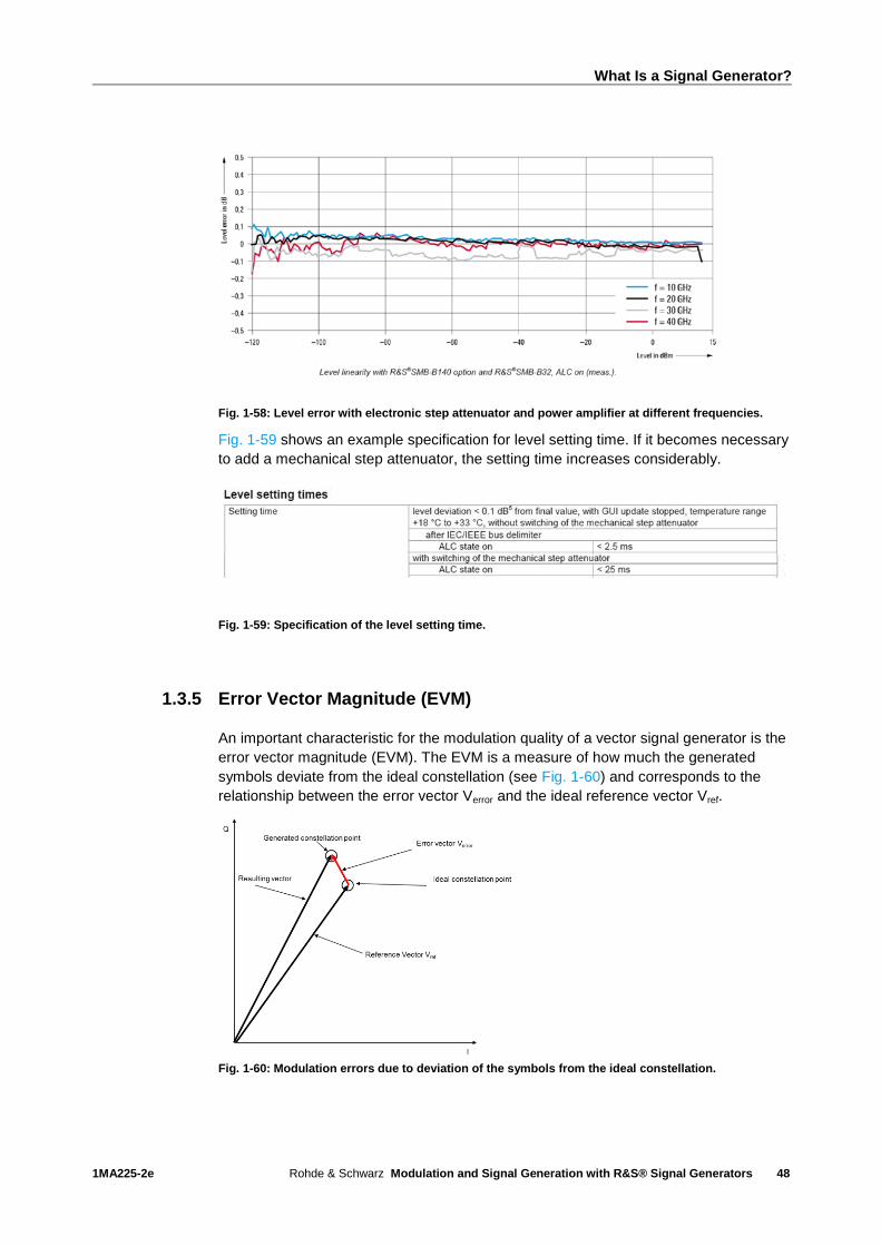
What Is a Signal Generator?
1MA225-2e Rohde & Schwarz Modulation and Signal Generation with R&S® Signal Generators
48
Fig. 1-58: Level error with electronic step attenuator and power amplifier at different frequencies.
Fig. 1-59 shows an example specification for level setting time. If it becomes necessary
to add a mechanical step attenuator, the setting time increases considerably.
Fig. 1-59: Specification of the level setting time.
1.3.5 Error Vector Magnitude (EVM)
An important characteristic for the modulation quality of a vector signal generator is the
error vector magnitude (EVM). The EVM is a measure of how much the generated
symbols deviate from the ideal constellation (see Fig. 1-60) and corresponds to the
relationship between the error vector Verror and the ideal reference vector Vref.
Fig. 1-60: Modulation errors due to deviation of the symbols from the ideal constellation.
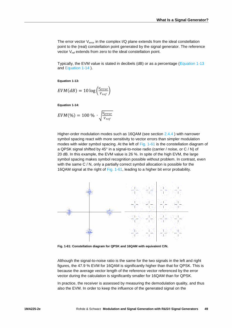
What Is a Signal Generator?
1MA225-2e Rohde & Schwarz Modulation and Signal Generation with R&S® Signal Generators
49
The error vector Verror in the complex I/Q plane extends from the ideal constellation
point to the (real) constellation point generated by the signal generator. The reference
vector Vref extends from zero to the ideal constellation point.
Typically, the EVM value is stated in decibels (dB) or as a percentage (Equation 1-13 and Equation 1-14 ). Equation 1-13:
𝐸𝑉𝑀(𝑑𝐵) = 10 log (𝑉𝑒𝑟𝑟𝑜𝑟
𝑉𝑟𝑒𝑓)
Equation 1-14:
𝐸𝑉𝑀(%) = 100 % ∙ √𝑉𝑒𝑟𝑟𝑜𝑟
𝑉𝑟𝑒𝑓
Higher-order modulation modes such as 16QAM (see section 2.4.4 ) with narrower
symbol spacing react with more sensitivity to vector errors than simpler modulation
modes with wider symbol spacing. At the left of Fig. 1-61 is the constellation diagram of
a QPSK signal shifted by 45° in a signal-to-noise radio (carrier / noise, or C / N) of
20 dB. In this example, the EVM value is 26 %. In spite of the high EVM, the large
symbol spacing makes symbol recognition possible without problem. In contrast, even
with the same C / N, only a partially correct symbol allocation is possible for the
16QAM signal at the right of Fig. 1-61, leading to a higher bit error probability.
Fig. 1-61: Constellation diagram for QPSK and 16QAM with equivalent C/N.
Although the signal-to-noise ratio is the same for the two signals in the left and right
figures, the 47.9 % EVM for 16QAM is significantly higher than that for QPSK. This is
because the average vector length of the reference vector referenced by the error
vector during the calculation is significantly smaller for 16QAM than for QPSK.
In practice, the receiver is assessed by measuring the demodulation quality, and thus
also the EVM. In order to keep the influence of the generated signal on the

What Is a Signal Generator?
1MA225-2e Rohde & Schwarz Modulation and Signal Generation with R&S® Signal Generators
50
measurement result to a minimum, it is therefore important that the signal generator
produce a signal with a high modulation quality, i.e. a low EVM. The EVM of a vector
signal generator depends on the baseband filtering, modulation mode, symbol rate
and, for mobile radio signals, also on the selected mobile cellular standard (see also
excerpt from a data sheet in Fig. 1-62).
Fig. 1-62: Example of an EVM specification.
1.3.6 Adjacent Channel Power (ACP)
In order to ensure that transmitted information is received without interference by as
many subscribers as possible, the adjacent channels in the frequency domain must
always remain free of interference. One measure for this interference is the adjacent
channel power, which should remain as low as possible and which is stated either as
an absolute value (in dBm) or as a relative value referenced to the channel power in
the transmission channel. The adjacent channel power (ACP) is also known as
adjacent channel leakage power ratio (ACLR) or the adjacent channel power ratio
(ACPR). The unwanted spurious emissions are primarily caused by amplifiers and their
third-order intermodulation products in the first adjacent channel as well as by fifth-
order intermodulation products in the second adjacent channel (the alternate channel).
In order to test the amplifiers for generated disturbance power in the adjacent channel,
it is important that the test signal produced by the vector signal generator itself have a
very high adjacent channel power suppression. The ACPR value is therefore another
important quality characteristic for a vector signal generator. As seen in the data sheet
excerpt in the figure below, this value is also dependent on the generated signal and
on the selected standard.
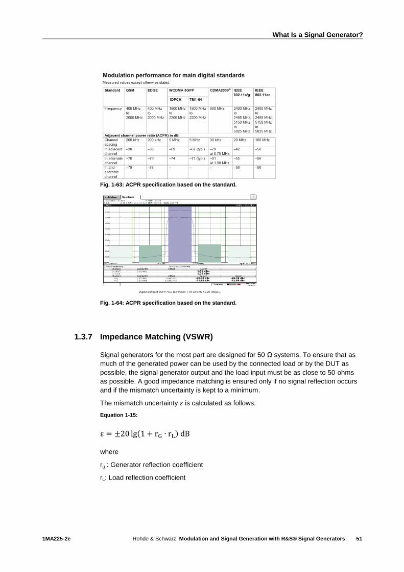
What Is a Signal Generator?
1MA225-2e Rohde & Schwarz Modulation and Signal Generation with R&S® Signal Generators
51
Fig. 1-63: ACPR specification based on the standard.
Fig. 1-64: ACPR specification based on the standard.
1.3.7 Impedance Matching (VSWR)
Signal generators for the most part are designed for 50 Ω systems. To ensure that as
much of the generated power can be used by the connected load or by the DUT as
possible, the signal generator output and the load input must be as close to 50 ohms
as possible. A good impedance matching is ensured only if no signal reflection occurs
and if the mismatch uncertainty is kept to a minimum.
The mismatch uncertainty 𝜀 is calculated as follows:
Equation 1-15:
ε = ±20 lg(1 + rG ∙ rL) dB
where
rg : Generator reflection coefficient
rL: Load reflection coefficient
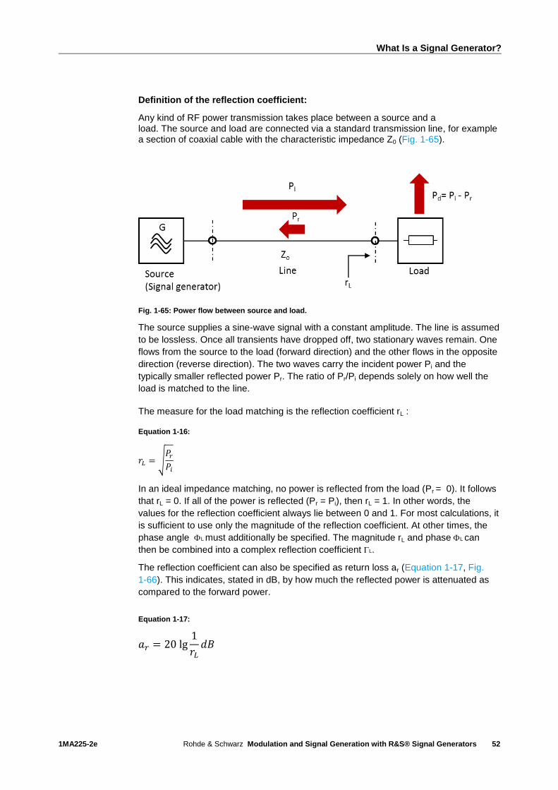
What Is a Signal Generator?
1MA225-2e Rohde & Schwarz Modulation and Signal Generation with R&S® Signal Generators
52
Definition of the reflection coefficient:
Any kind of RF power transmission takes place between a source and a load. The source and load are connected via a standard transmission line, for example a section of coaxial cable with the characteristic impedance Z0 (Fig. 1-65).
Fig. 1-65: Power flow between source and load.
The source supplies a sine-wave signal with a constant amplitude. The line is assumed
to be lossless. Once all transients have dropped off, two stationary waves remain. One
flows from the source to the load (forward direction) and the other flows in the opposite
direction (reverse direction). The two waves carry the incident power Pi and the
typically smaller reflected power Pr. The ratio of Pr/Pi depends solely on how well the
load is matched to the line.
The measure for the load matching is the reflection coefficient rL : Equation 1-16:
𝑟𝐿 = √𝑃𝑟
𝑃𝑖
In an ideal impedance matching, no power is reflected from the load (Pr = 0). It follows
that rL = 0. If all of the power is reflected (Pr = Pi), then rL = 1. In other words, the
values for the reflection coefficient always lie between 0 and 1. For most calculations, it
is sufficient to use only the magnitude of the reflection coefficient. At other times, the
phase angle L must additionally be specified. The magnitude rL and phase L can
then be combined into a complex reflection coefficient L.
The reflection coefficient can also be specified as return loss ar (Equation 1-17, Fig.
1-66). This indicates, stated in dB, by how much the reflected power is attenuated as
compared to the forward power.
Equation 1-17:
𝑎𝑟 = 20 lg 1
𝑟𝐿𝑑𝐵

What Is a Signal Generator?
1MA225-2e Rohde & Schwarz Modulation and Signal Generation with R&S® Signal Generators
53
As seen in Fig. Fig. 1-65, the load receives only the net difference between the forward
power and the reflected power. It is therefore also known as the net power or the
absorbed power Pd:
Equation 1-18:
𝑃𝑑 = 𝑃𝑖 + 𝑃𝑟
The specifications for a signal generator output typically include the impedance
matching but not the reflection coefficient. Another typical measure for the impedance
matching is the voltage standing wave ratio (VSWR).
Definition of VSWR:
The interference pattern resulting from the superposition of forward and reflected
waves is called a standing wave. It is periodic with one half a line wavelength. At the
positions where the voltage and current of both waves are either in phase or out of
phase, maxima and minima values are produced. The ratio of maximum to minimum
values is a measure of the magnitude of the load-side reflection coefficient. This ripple
s and the extreme values can be very precisely determined on transmission lines.
More commonly used than the term "ripple" is the term voltage standing wave ratio
(VSWR), or simply SWR. Unlike the reflection coefficient, the VSWR is calculated not
from the power ratio, but rather from the maximum and minimum voltage values of the
standing wave. The following definition applies for s, or VSWR:
Equation 1-19:
𝑠 = 𝑉𝑆𝑊𝑅 = 𝑆𝑊𝑅 =𝑉𝑚𝑎𝑥
𝑉𝑚𝑖𝑛
The VSWR and the reflection coefficient have the following relationship:
Equation 1-20:
𝑉𝑆𝑊𝑅 =1 + 𝑟𝐿
1 − 𝑟𝐿
For impedance matching where rL = 0, the result is VSWR = 1. For total reflection
where rL = 1, the result is VSWR = ∞. The value range for VSWR therefore lies
between 0 and ∞ (see also Fig. 1-66).

What Is a Signal Generator?
1MA225-2e Rohde & Schwarz Modulation and Signal Generation with R&S® Signal Generators
54
Fig. 1-66: Conversion table for reflection coefficient r, return loss ar and standing wave ratio VSWR.
The abbreviation VSWR is so widely used that it has also come to describe the source-
side impedance matching. However, that is not to say that the concept of replacing rL
with rG in Equation 1-20 is merely semantics, with no foundation in physical science.
The following equation can also be used for the VSWR of a signal generator:
Equation 1-21:
𝑉𝑆𝑊𝑅 =1 + 𝑟𝐺
1– 𝑟𝐺
Because the type of step attenuators used in the signal generator can have an effect
on the generator matching, the VSWR value is typically specified for several different
instrument configurations. Fig. 1-67 provides an example from a data sheet for a signal
generator.
Fig. 1-67: Excerpt from the R&S® SMB100A signal generator data sheet.
In the following example, the mismatch uncertainty of a signal generator is calculated
with a connected load, or DUT.
Impedance matching for the generator : VSWRG= 1.6 (R&S® SMB100A up to 20 GHz)
Impedance matching for the load: VSWRL= 1.7
To make it possible to calculate the mismatch uncertainty using Equation 1-15, the reflection coefficients rG and rL are calculated from the known VSWR as follows after solving Equation 1-20 and
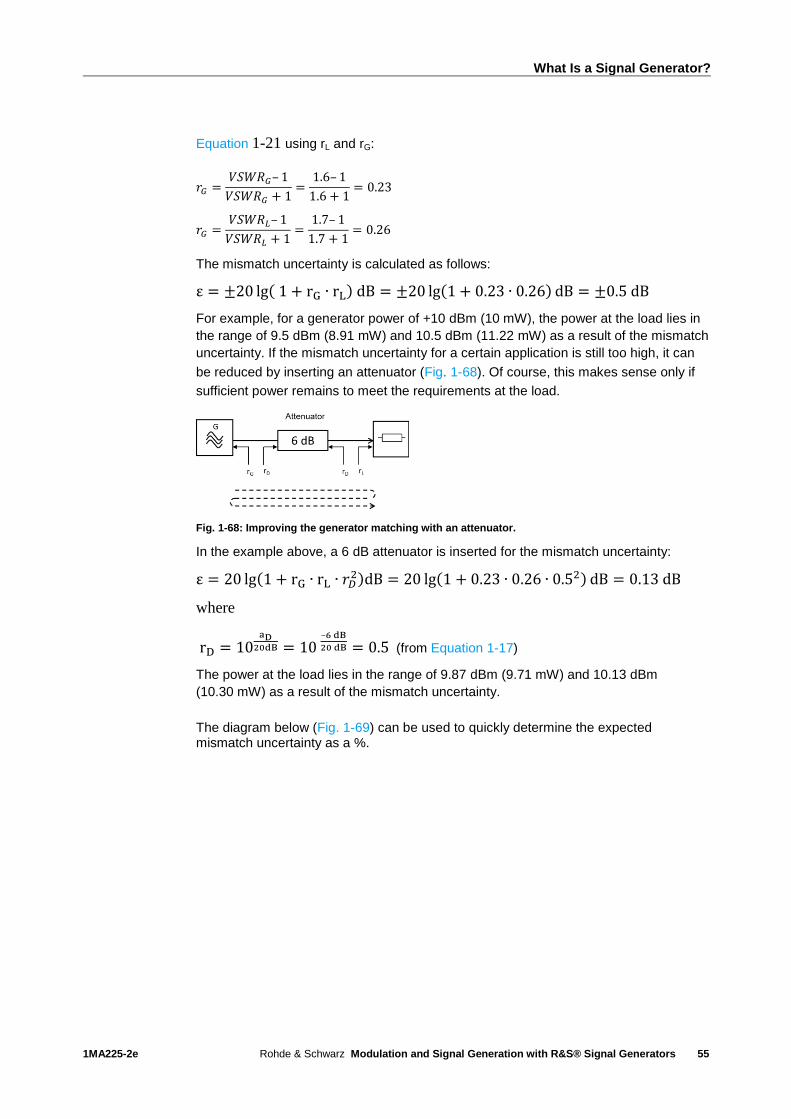
What Is a Signal Generator?
1MA225-2e Rohde & Schwarz Modulation and Signal Generation with R&S® Signal Generators
55
Equation 1-21 using rL and rG:
𝑟𝐺 =𝑉𝑆𝑊𝑅𝐺– 1
𝑉𝑆𝑊𝑅𝐺 + 1=
1.6– 1
1.6 + 1= 0.23
𝑟𝐺 =𝑉𝑆𝑊𝑅𝐿– 1
𝑉𝑆𝑊𝑅𝐿 + 1=
1.7– 1
1.7 + 1= 0.26
The mismatch uncertainty is calculated as follows:
ε = ±20 lg( 1 + rG ∙ rL) dB = ±20 lg(1 + 0.23 ∙ 0.26) dB = ±0.5 dB
For example, for a generator power of +10 dBm (10 mW), the power at the load lies in
the range of 9.5 dBm (8.91 mW) and 10.5 dBm (11.22 mW) as a result of the mismatch
uncertainty. If the mismatch uncertainty for a certain application is still too high, it can
be reduced by inserting an attenuator (Fig. 1-68). Of course, this makes sense only if
sufficient power remains to meet the requirements at the load.
Fig. 1-68: Improving the generator matching with an attenuator.
In the example above, a 6 dB attenuator is inserted for the mismatch uncertainty:
ε = 20 lg(1 + rG ∙ rL ∙ 𝑟𝐷2)dB = 20 lg(1 + 0.23 ∙ 0.26 ∙ 0.52) dB = 0.13 dB
where
rD = 10aD
20dB = 10 –6 dB
20 dB = 0.5 (from Equation 1-17)
The power at the load lies in the range of 9.87 dBm (9.71 mW) and 10.13 dBm
(10.30 mW) as a result of the mismatch uncertainty.
The diagram below (Fig. 1-69) can be used to quickly determine the expected mismatch uncertainty as a %.

What Is a Signal Generator?
1MA225-2e Rohde & Schwarz Modulation and Signal Generation with R&S® Signal Generators
56
Fig. 1-69: Mismatch uncertainty for the forward power and for the power available at Z0.

Modulation Methods
1MA225-2e Rohde & Schwarz Modulation and Signal Generation with R&S® Signal Generators
57
2 Modulation Methods
In order to transmit electrical information signals efficiently and with as little distortion
as possible, the signals must be adapted to the physical characteristics of the
transmission channel. To do this, the amplitude, frequency or phase angle of a carrier
signal is modified by the wanted signal (voice, music, data) to permit efficient utilization
of the transmission channel. This process is known as modulation. Within the carrier
frequency range, the transmit signal occupies a bandwidth that is dependent on the
wanted signal. The carrier signal itself has no significance with respect to the
transmitted message and can be suppressed for certain modulation modes. Because
only high-frequency signals can be radiated as electromagnetic waves over an
antenna, the wireless transmission of signals requires a modulated, high-frequency
carrier. On the receiver end, the wanted signal is restored by means of a demodulator
(Fig. 2-1). The transmission channel can involve a conducted transmission over
electrical or fiber-optic cables, or it can involve a radio link via antennas.
Fig. 2-1: Signal path during the transmission of information using modulated signals.
Continuous-time modulation methods use a continuous signal, such as a sine-wave
oscillation, as the carrier. The two varieties of continuous-time methods are continuous
value modulation and discrete value modulation. The continuous-value influence of a
time-continuous carrier is better known as analog modulation, while a discrete-value
influence of the carrier is known as digital modulation.
To better utilize the transmission channel, wanted signals are transmitted in parallel
over a common channel by means of multiplexing. The practical implementation of the
various multiplexing methods, including time-division multiplexing, frequency-division
multiplexing and code-division multiplexing, is likewise achieved through the use of the
appropriate modulation methods.
2.1 Analog Modulation Methods
Analog modulations continuously process analog wanted signals such as voice, music
or video signals without digitizing the transmission signal values. There are two main
types of analog modulation, amplitude modulation and angle modulation. All other
analog modulation methods are derived from these two modulation techniques. Table
2-1 shows the most important types of analog modulation.
Type of modulation Abbreviation
Amplitude modulation AM
Single-sideband modulation SSB-AM
Vestigial-sideband modulation VSB-AM Double-sideband suppressed carrier DSBSC-AM
Frequency modulation FM
Phase modulation PM
Table 2-1: Summary of the most important types of analog modulation
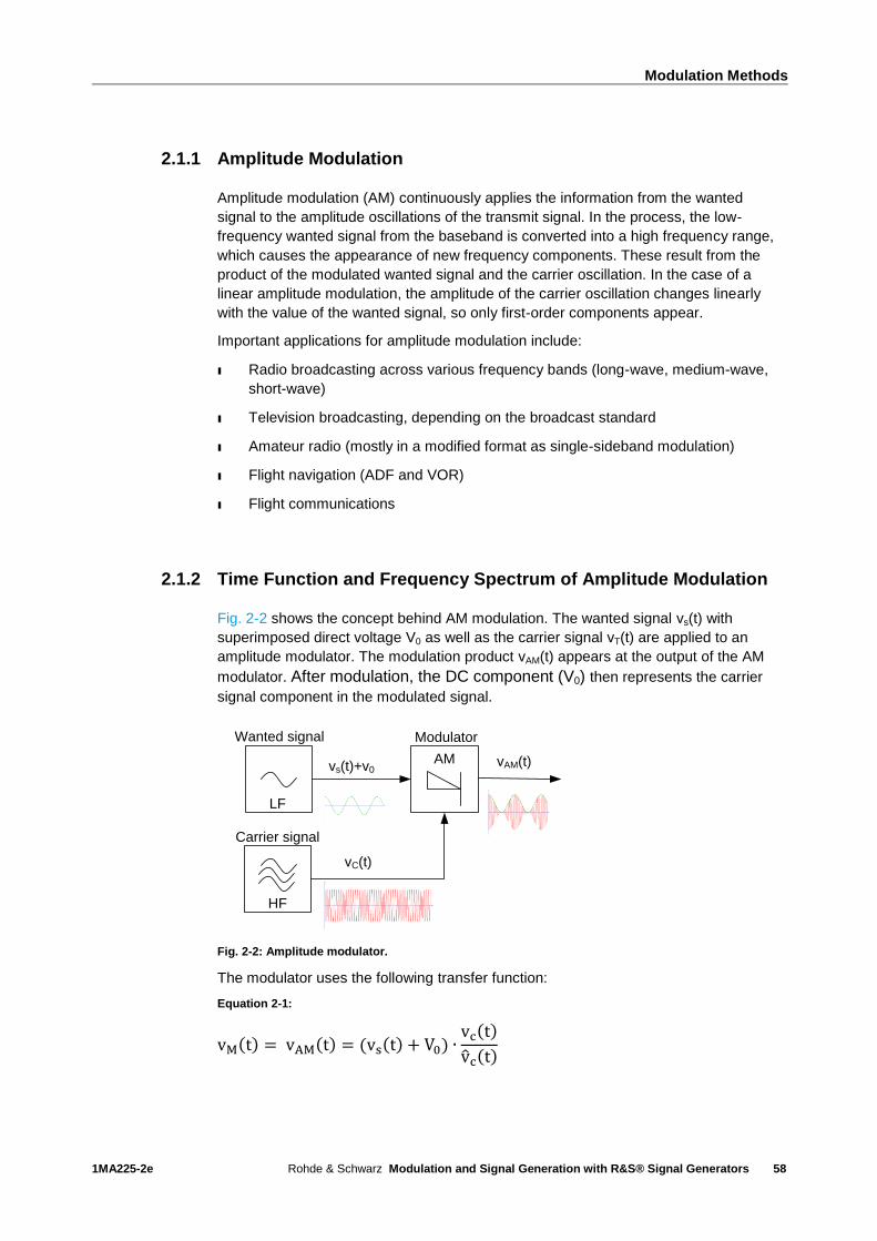
Modulation Methods
1MA225-2e Rohde & Schwarz Modulation and Signal Generation with R&S® Signal Generators
58
2.1.1 Amplitude Modulation
Amplitude modulation (AM) continuously applies the information from the wanted
signal to the amplitude oscillations of the transmit signal. In the process, the low-
frequency wanted signal from the baseband is converted into a high frequency range,
which causes the appearance of new frequency components. These result from the
product of the modulated wanted signal and the carrier oscillation. In the case of a
linear amplitude modulation, the amplitude of the carrier oscillation changes linearly
with the value of the wanted signal, so only first-order components appear.
Important applications for amplitude modulation include:
ı Radio broadcasting across various frequency bands (long-wave, medium-wave,
short-wave)
ı Television broadcasting, depending on the broadcast standard
ı Amateur radio (mostly in a modified format as single-sideband modulation)
ı Flight navigation (ADF and VOR)
ı Flight communications
2.1.2 Time Function and Frequency Spectrum of Amplitude Modulation
Fig. 2-2 shows the concept behind AM modulation. The wanted signal vs(t) with
superimposed direct voltage V0 as well as the carrier signal vT(t) are applied to an
amplitude modulator. The modulation product vAM(t) appears at the output of the AM
modulator. After modulation, the DC component (V0) then represents the carrier
signal component in the modulated signal.
HF
Carrier signal
Wanted signal
LF
Modulator
vs(t)+v0
vC(t)
vAM(t)AM
Fig. 2-2: Amplitude modulator.
The modulator uses the following transfer function:
Equation 2-1:
vM(t) = vAM(t) = (vs(t) + V0) ∙vc(t)
vc(t)
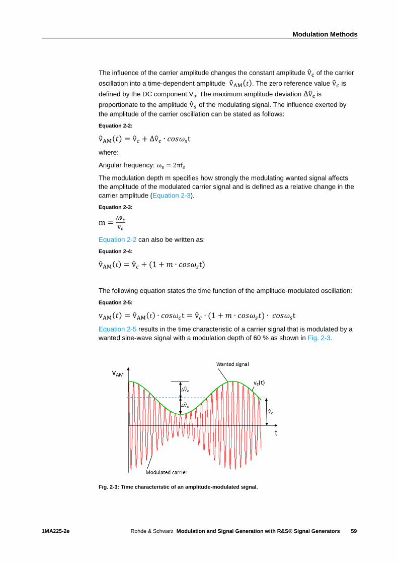
Modulation Methods
1MA225-2e Rohde & Schwarz Modulation and Signal Generation with R&S® Signal Generators
59
The influence of the carrier amplitude changes the constant amplitude vc of the carrier
oscillation into a time-dependent amplitude vAM(𝑡). The zero reference value v𝑐 is
defined by the DC component Vo. The maximum amplitude deviation ∆vc is
proportionate to the amplitude vs of the modulating signal. The influence exerted by
the amplitude of the carrier oscillation can be stated as follows:
Equation 2-2:
vAM(𝑡) = v𝑐 + ∆vc ∙ 𝑐𝑜𝑠𝜔𝑠t
where:
Angular frequency: ωs = 2πf𝑠
The modulation depth m specifies how strongly the modulating wanted signal affects
the amplitude of the modulated carrier signal and is defined as a relative change in the
carrier amplitude (Equation 2-3).
Equation 2-3:
m =∆v𝑐
v𝑐
Equation 2-2 can also be written as:
Equation 2-4:
vAM(𝑡) = v𝑐 + (1 + 𝑚 ∙ 𝑐𝑜𝑠𝜔𝑠t)
The following equation states the time function of the amplitude-modulated oscillation:
Equation 2-5:
vAM(𝑡) = vAM(𝑡) ∙ 𝑐𝑜𝑠𝜔𝑐t = v𝑐 ∙ (1 + 𝑚 ∙ 𝑐𝑜𝑠𝜔𝑠𝑡) ∙ 𝑐𝑜𝑠𝜔𝑠t
Equation 2-5 results in the time characteristic of a carrier signal that is modulated by a
wanted sine-wave signal with a modulation depth of 60 % as shown in Fig. 2-3.
Fig. 2-3: Time characteristic of an amplitude-modulated signal.
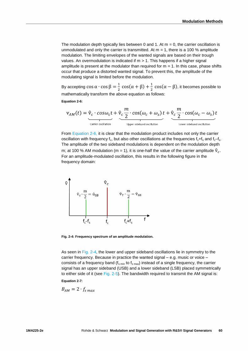
Modulation Methods
1MA225-2e Rohde & Schwarz Modulation and Signal Generation with R&S® Signal Generators
60
The modulation depth typically lies between 0 and 1. At m = 0, the carrier oscillation is
unmodulated and only the carrier is transmitted. At m = 1, there is a 100 % amplitude
modulation. The limiting envelopes of the wanted signals are based on their trough
values. An overmodulation is indicated if m > 1. This happens if a higher signal
amplitude is present at the modulator than required for m = 1. In this case, phase shifts
occur that produce a distorted wanted signal. To prevent this, the amplitude of the
modulating signal is limited before the modulation.
By accepting cos α ∙ cos β =1
2 cos(α + β) +
1
2 cos(α − β), it becomes possible to
mathematically transform the above equation as follows:
Equation 2-6:
From Equation 2-6, it is clear that the modulation product includes not only the carrier
oscillation with frequency fc, but also other oscillations at the frequencies fc+fs and fc–fs.
The amplitude of the two sideband modulations is dependent on the modulation depth
m; at 100 % AM modulation (m = 1), it is one-half the value of the carrier amplitude v𝑐 .
For an amplitude-modulated oscillation, this results in the following figure in the
frequency domain:
Fig. 2-4: Frequency spectrum of an amplitude modulation.
As seen in Fig. 2-4, the lower and upper sideband oscillations lie in symmetry to the
carrier frequency. Because in practice the wanted signal – e.g. music or voice –
consists of a frequency band (fs min to fs max) instead of a single frequency, the carrier
signal has an upper sideband (USB) and a lower sideband (LSB) placed symmetrically
to either side of it (see Fig. 2-5). The bandwidth required to transmit the AM signal is:
Equation 2-7:
𝐵𝐴𝑀 = 2 ∙ 𝑓𝑠 𝑚𝑎𝑥
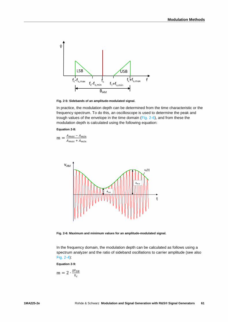
Modulation Methods
1MA225-2e Rohde & Schwarz Modulation and Signal Generation with R&S® Signal Generators
61
Fig. 2-5: Sidebands of an amplitude-modulated signal.
In practice, the modulation depth can be determined from the time characteristic or the
frequency spectrum. To do this, an oscilloscope is used to determine the peak and
trough values of the envelope in the time domain (Fig. 2-6), and from these the
modulation depth is calculated using the following equation:
Equation 2-8:
m =𝐴𝑚𝑎𝑥 − 𝐴𝑚𝑖𝑛
𝐴𝑚𝑎𝑥 + 𝐴𝑚𝑖𝑛
Fig. 2-6: Maximum and minimum values for an amplitude-modulated signal.
In the frequency domain, the modulation depth can be calculated as follows using a
spectrum analyzer and the ratio of sideband oscillations to carrier amplitude (see also
Fig. 2-4):
Equation 2-9:
m = 2 ∙∆v𝑆𝐵
v𝑐

Modulation Methods
1MA225-2e Rohde & Schwarz Modulation and Signal Generation with R&S® Signal Generators
62
Usually a spectrum analyzer displays the signal amplitudes on a logarithmic scale (Fig.
2-7). From the delta ∆L between the carrier level Lc and the sideband oscillation level
LSB, the modulation depth can be calculated using Equation 2-10 without converting to
linear values.
Equation 2-10:
m = 10(6 𝑑𝐵−∆𝐿
20 𝑑𝐵)
Fig. 2-7: Logarithmic frequency spectrum of an amplitude-modulated signal.
Another way to determine the modulation depth is to use the trapezoid method. This is
done by operating the oscilloscope in XY mode. The horizontal deflection (X-deflection)
of the modulating signal vs(t) and the vertical deflection (Y-deflection) of the amplitude-
modulated signal vAM(t) are applied. Displayed as an oscillogram, for m < 1 a trapezoid
results with sides 2 ∙ Amax and 2 ∙ Amin. (Modulation depth calculated using Equation
2-8). For m = 1, the trapezoid changes to a triangle (Amin = 0). With overmodulation
(m > 1), an extension of the triangle can be seen (Fig. 2-8).
Fig. 2-8: Modulation trapezoid at various modulation depths.
If a phase shift lies between the modulating signal and the envelope, the upper and
lower boundaries of the trapezoid are represented by an ellipse (Fig. 2-9).
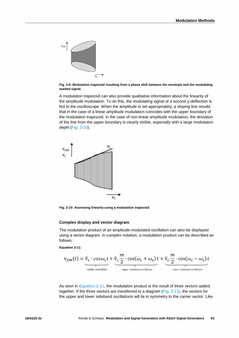
Modulation Methods
1MA225-2e Rohde & Schwarz Modulation and Signal Generation with R&S® Signal Generators
63
Fig. 2-9: Modulation trapezoid resulting from a phase shift between the envelope and the modulating
wanted signal.
A modulation trapezoid can also provide qualitative information about the linearity of
the amplitude modulation. To do this, the modulating signal of a second y-deflection is
fed to the oscilloscope. When the amplitude is set appropriately, a sloping line results
that in the case of a linear amplitude modulation coincides with the upper boundary of
the modulation trapezoid. In the case of non-linear amplitude modulation, the deviation
of the line from the upper boundary is clearly visible, especially with a large modulation
depth (Fig. 2-10).
Fig. 2-10: Assessing linearity using a modulation trapezoid.
Complex display and vector diagram
The modulation product of an amplitude-modulated oscillation can also be displayed
using a vector diagram. In complex notation, a modulation product can be described as
follows:
Equation 2-11:
As seen in Equation 2-11, the modulation product is the result of three vectors added
together. If the three vectors are transferred to a diagram (Fig. 2-11), the vectors for
the upper and lower sideband oscillations will lie in symmetry to the carrier vector. Like
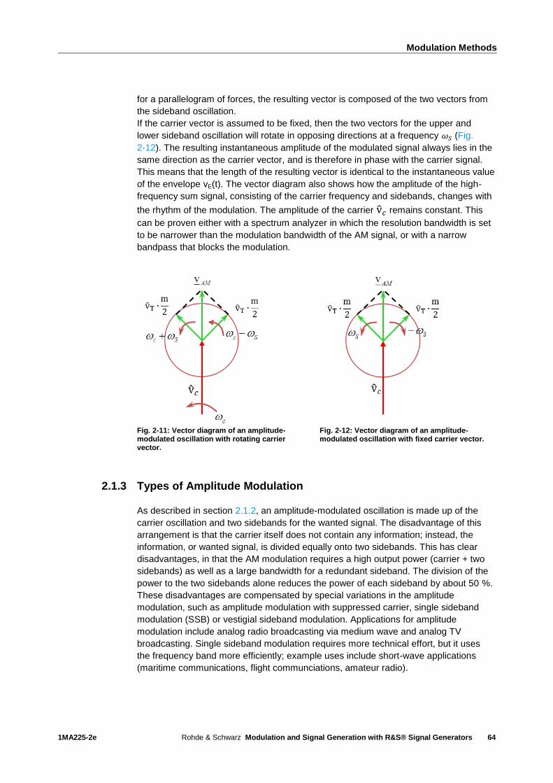
Modulation Methods
1MA225-2e Rohde & Schwarz Modulation and Signal Generation with R&S® Signal Generators
64
for a parallelogram of forces, the resulting vector is composed of the two vectors from
the sideband oscillation.
If the carrier vector is assumed to be fixed, then the two vectors for the upper and
lower sideband oscillation will rotate in opposing directions at a frequency 𝜔𝑆 (Fig.
2-12). The resulting instantaneous amplitude of the modulated signal always lies in the
same direction as the carrier vector, and is therefore in phase with the carrier signal.
This means that the length of the resulting vector is identical to the instantaneous value
of the envelope vE(t). The vector diagram also shows how the amplitude of the high-
frequency sum signal, consisting of the carrier frequency and sidebands, changes with
the rhythm of the modulation. The amplitude of the carrier v𝑐 remains constant. This
can be proven either with a spectrum analyzer in which the resolution bandwidth is set
to be narrower than the modulation bandwidth of the AM signal, or with a narrow
bandpass that blocks the modulation.
Fig. 2-11: Vector diagram of an amplitude-modulated oscillation with rotating carrier vector.
Fig. 2-12: Vector diagram of an amplitude-modulated oscillation with fixed carrier vector.
2.1.3 Types of Amplitude Modulation
As described in section 2.1.2, an amplitude-modulated oscillation is made up of the
carrier oscillation and two sidebands for the wanted signal. The disadvantage of this
arrangement is that the carrier itself does not contain any information; instead, the
information, or wanted signal, is divided equally onto two sidebands. This has clear
disadvantages, in that the AM modulation requires a high output power (carrier + two
sidebands) as well as a large bandwidth for a redundant sideband. The division of the
power to the two sidebands alone reduces the power of each sideband by about 50 %.
These disadvantages are compensated by special variations in the amplitude
modulation, such as amplitude modulation with suppressed carrier, single sideband
modulation (SSB) or vestigial sideband modulation. Applications for amplitude
modulation include analog radio broadcasting via medium wave and analog TV
broadcasting. Single sideband modulation requires more technical effort, but it uses
the frequency band more efficiently; example uses include short-wave applications
(maritime communications, flight communciations, amateur radio).
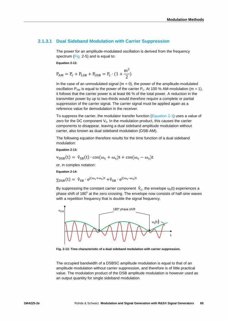
Modulation Methods
1MA225-2e Rohde & Schwarz Modulation and Signal Generation with R&S® Signal Generators
65
2.1.3.1 Dual Sideband Modulation with Carrier Suppression
The power for an amplitude-modulated oscillation is derived from the frequency
spectrum (Fig. 2-5) and is equal to:
Equation 2-12:
PAM = Pc + PLSB + PUSB = Pc ∙ (1 +m2
2)
In the case of an unmodulated signal (m = 0), the power of the amplitude-modulated
oscillation PAM is equal to the power of the carrier Pc. At 100 % AM-modulation (m = 1),
it follows that the carrier power is at least 66 % of the total power. A reduction in the
transmitter power by up to two-thirds would therefore require a complete or partial
suppression of the carrier signal. The carrier signal must be applied again as a
reference value for demodulation in the receiver.
To suppress the carrier, the modulator transfer function (Equation 2-1) uses a value of
zero for the DC component V0. In the modulation product, this causes the carrier
components to disappear, leaving a dual sideband amplitude modulation without
carrier, also known as dual sideband modulation (DSB-AM).
The following equation therefore results for the time function of a dual sideband
modulation:
Equation 2-13:
vDSB(t) = vSB(t) ∙ cos(ωc + ωs)t + cos(ωc − ωs)t
or, in complex notation:
Equation 2-14:
vDSB(t) = vSB ∙ ej(ωc+ωs)t +vSB ∙ ej(ωc–ωs)t
By suppressing the constant carrier component vc, the envelope uE(t) experiences a
phase shift of 180o at the zero crossing. The envelope now consists of half-sine waves
with a repetition frequency that is double the signal frequency.
Fig. 2-13: Time characteristic of a dual sideband modulation with carrier suppression.
The occupied bandwidth of a DSBSC amplitude modulation is equal to that of an
amplitude modulation without carrier suppression, and therefore is of little practical
value. The modulation product of the DSB amplitude modulation is however used as
an output quantity for single sideband modulation.

Modulation Methods
1MA225-2e Rohde & Schwarz Modulation and Signal Generation with R&S® Signal Generators
66
2.1.3.2 Single Sideband Modulation
In order to reduce the required bandwidth, only one sideband is used for single
sideband amplitude modulation (SSB-AM). This is done by suppressing the second
sideband. This is possible because both sidebands contain the same information. In
addition to the bandwidth advantage, a SSB modulation can apply all of the transmit
energy to the information contained in the signal. The result is an increased coverage
and a greater signal-to-noise ratio at the same transmit power. In many cases, the
transmission includes not only the sidebands, but also a residual carrier as a reference
quantity for the demodulation. The highly accurate transmit and receive oscillators
available today make this type of modulation of little significance, however.
2.1.3.3 Vestigial Sideband Modulation
When vestigial sideband modulation is used to transmit information signals with very
small frequency components, a filter with a very steep edge slope must be used to
suppress the unwanted sidebands. Apart from the high technical effort to implement,
steep-edged filters have the disadvantage that they exhibit a strong group delay at the
boundary to the passband. Pulsed signals in particular are strongly distorted during
transmission. A vestigial sideband modulation (VSB-AM) can help. This is
accomplished by using filters whose transfer function has a relatively flat falling edge.
The ensures that a portion of the sideband that is to be suppressed (vestigial
sideband) is included in the transmission (Fig. 2-14).
Fig. 2-14: Partial suppression of the lower sideband during vestigial sideband modulation.
Because VSB-AM causes the entire upper sideband and a portion of the lower
sideband to be transmitted, the signal amplitudes of the low and high frequencies are
significantly different after demodulation. To compensate, a filter with a Nyquist edge is
used before the demodulation. The carrier frequency lies about halfway on the sloping
filter edge (Fig. 2-15). At high signal frequencies, this filter provides less amplification
within the lower frequency range on the upper sideband than it does at the upper
frequencies. This dissipation is eliminated by the portion of the lower sideband that lies
below the Nyquist edge. As a result, a signal with a compensated amplitude frequency
response can be supplied to the demodulator. The restored information is for the most
part free of linear distortion. One use for VSB-AM is transmitting vision carriers. The
edge width of the Nyquist filter in a television receiver is 1.5 MHz.

Modulation Methods
1MA225-2e Rohde & Schwarz Modulation and Signal Generation with R&S® Signal Generators
67
Fig. 2-15: Frequency response compensation using a filter with a Nyquist edge on the receive end.
2.1.4 Angle Modulation
Unlike amplitude modulation where the amplitude is modified, angle modulation
modifies the phase angle of a carrier oscillation dependent on the wanted signal.
Because this causes a simultaneous change in the carrier frequency, the angle
modulation can be considered a type of phase modulation (PM) or frequency
modulation. The distinctions are described in more detail in section 2.1.6. With both
modulations, the amplitude of the carrier signal remains constant.
Angle modulations, of which the primary types are frequency modulation (FM) and
phase modulation (PM), apply the wanted signal to the phase angle of the carrier
signal. This causes a change in the carrier frequency or the phase angle of the carrier
signal. Examples of applications for these technologies are found in analog VHF FM
radio broadcasting.
2.1.5 Time Function and Frequency Spectrum
Fig. 2-16 shows the principles behind angle modulation. The wanted signal vs(t) with
superimposed DC voltage V0 and the carrier signal vc(t) are fed to an angle modulator.
HF
Carrier signal
Wanted signal
NF
Modulator
vs(t)+V0
vc(t)
vAngleMod(t)
Fig. 2-16: Angle modulator.
The starting point for angle modulation is a sine-wave carrier oscillation:
Equation 2-15:
v𝑐(𝑡) = v𝑐 ∙ 𝑐𝑜𝑠𝜔𝑐t = v𝑐 ∙ 𝑐𝑜𝑠𝜑𝑐(𝑡)
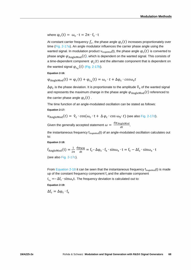
Modulation Methods
1MA225-2e Rohde & Schwarz Modulation and Signal Generation with R&S® Signal Generators
68
where φ𝑐(t) = ωc ∙ t = 2π ∙ fc ∙ t
At constant carrier frequency 𝑓𝑐, the phase angle 𝜑c(𝑡) increases proportionately over
time (Fig. 2-17a). An angle modulator influences the carrier phase angle using the
wanted signal. In modulation product vAngleMod(t), the phase angle 𝜑c(𝑡) is converted to
phase angle 𝜑AngleMod(𝑡), which is dependent on the wanted signal. This consists of
a time-dependent component 𝜑c(𝑡) and the alternate component that is dependent on
the wanted signal 𝜑𝑐𝑎(𝑡) (Fig. 2-17b).
Equation 2-16:
φAngleMod(t) = φ𝑐(t) + φ𝑐𝑎(t) = ωc ∙ 𝑡 + ∆φc ∙ 𝑐𝑜𝑠ωs𝑡
∆𝜑c is the phase deviation. It is proportionate to the amplitude vs of the wanted signal
and represents the maximum change in the phase angle 𝜑AngleMod(𝑡) referenced to
the carrier phase angle 𝜑c(𝑡) .
The time function of an angle-modulated oscillation can be stated as follows:
Equation 2-17:
uAngleMod(𝑡) = vc ∙ cos (ωc ∙ t + ∆ 𝜑c ∙ cos ωS∙ 𝑡) (see also Fig. 2-17d).
Given the generally accepted statement 𝜔 = 𝑑𝜑𝐴𝑛𝑔𝑙𝑒𝑀𝑜𝑑
𝑑𝑡,
the instantaneous frequency fAngleMod(t) of an angle-modulated oscillation calculates out
to:
Equation 2-18:
fAngleMod(t) =1
2π dφWM
dt= fc– ∆φc ∙ fs ∙ sinωs ∙ t = fc − ∆fc ∙ sinωs ∙ t
(see also Fig. 2-17c).
From Equation 2-18 it can be seen that the instantaneous frequency fAngleMod(t) is made
up of the constant frequency component fc and the alternate component
fca=– ∆fc ∙ sinωst. The frequency deviation is calculated out to:
Equation 2-19:
∆fc = ∆φc ∙ fs

Modulation Methods
1MA225-2e Rohde & Schwarz Modulation and Signal Generation with R&S® Signal Generators
69
Fig. 2-17: The phase angle and frequency of an angle-modulated signal based on the wanted signal.
a) Wanted signal, b) Phase angle, c) Frequency, d) Time function of the angle-modulated oscillation.
Like for amplitude modulation (see Equation 2-11), the equation for angle modulation
vAngleMod(t) can be used to derive a representation of the frequency spectrum. Because
a simple trigonometric transformation of the expression
cos (ωc ∙ t + ∆ φc ∙ cos ωc ∙ t) from Equation 2-17: is not possible, the derivation
requires the use of complex notation, followed by an application of the power series
expansion of the e-function. The full derivation will not be explained in more detail
here. The result of this method is:

Modulation Methods
1MA225-2e Rohde & Schwarz Modulation and Signal Generation with R&S® Signal Generators
70
Equation 2-20:
vAngleMod(t) = vc ∙ [J0(∆φC) ∙ cos ωct − J1(∆φc) ∙ [sin(ωc + ωs) t +
+ sin(ωc − ωs) t] − J2(∆φc) ∙ [cos(ωc + 2ωs) t + cos(ωc − 2ωs) t] +
+J3(∆φc) ∙ [sin(ωc + 3ωs) t + sin(ωc − 3ωs) t] + ⋯ ]
From the above equation, it can be seen that the spectrum of an angle-modulated
oscillation contains not only the carrier signal with frequency fc, but theoretically also an
infinite number of discrete sideband oscillations at the frequencies fc ± n ∙ fs in
symmetry to the carrier frequency. The amplitudes of the individual frequency
components are calculated from the Bessel function values of the first kind 𝐽𝑛(∆𝜑c)
and the nth kind (Fig. 2-18). Even where the Bessel functions have negative values,
the amplitude values of the two side lines are displayed as positive numbers in the
spectrum. In the phase diagram, this is indicated by a phase shift of 180°.
Fig. 2-18: Bessel function 𝑱𝒏(∆𝝋𝐜) for n=0 to 7 over a range from ∆𝝋𝐜 = 𝟎 𝒕𝒐 ∆𝝋𝐜 = 𝟏𝟎
The example values in Fig. 2-18 for ∆𝜑c (∆𝜑c = 1, blue; ∆𝜑c = 2.4 red) result in the
spectra shown in Fig. 2-19 for a sine-wave, angle-modulated oscillation.
Fig. 2-19: Frequency spectra for an angle-modulated oscillation at various phase deviations. ∆𝝋𝐓
As seen from the Bessel functions, the carrier oscillation or individual sideband
oscillations can range from ∆𝜑c to zero at certain values. For example, at ∆𝜑c = 2.4,
the carrier component disappears completely from the spectrum. It can also be seen
Modulation Methods
1MA225-2e Rohde & Schwarz Modulation and Signal Generation with R&S® Signal Generators
71
that the carrier amplitude depends on the phase deviation and therefore takes on the
larger value when unmodulated (∆𝜑c = 0).
Per Equation 2-20, the bandwidth of an angle-modulated signal can be very large. In
particular, an increase in the phase deviation will cause ever more sideband
oscillations to appear. In practice, therefore, the bandwidth is considered to be finite.
This includes all spectral lines up to around 10 % or 1 % of the carrier amplitude. As a
result, 90 % or 99 % of the spectral lines lie within the bandwidths calculated with
Equation 2-21 or Equation 2-22.
Equation 2-21:
BAngleMod10%= 2 ∙ fsmax
∙ (∆φ𝑐 + 1) for average transmission quality
Equation 2-22:
BAngleMod1%= 2 ∙ fsmax
∙ (∆φTc + 2) for high transmission quality
This means that the bandwidth of an angle-modulated signal (∆𝜑c > 0) is always
greater than the bandwidth of an amplitude-modulated signal.
2.1.6 Differentiation of Frequency versus Phase Modulation in Angle
Modulation
In angle modulation, frequency modulation (FM) and phase modulation (PM) occur
simultaneously. The instantaneous phase angle φAngleMod(t) is calculated as shown in
Equation 2-16 and the instantaneous frequency fAngleMod(t) is calculated as shown in
Equation 2-18. There is a fundamental link between the frequency deviation and the
phase deviation
as described in Equation 2-19: ∆fc = ∆φc ∙ fs
In practice, however, a distinction is made between FM and PM during angle
modulation. The difference lies in how the modulation product for an angle-modulated
oscillation is generated. It is not possible to tell from the modulation product or the
representation as a time function vAngleMod(t) whether an FM or a PM is involved.
However, it is possible to distinguish between the two by studying the spectrum at
different frequencies of a wanted sine-wave signal. As seen in Fig. 2-20, a change in
the wanted signal frequency causes a change in the spectral line spacing for both FM
and for PM. In phase modulation, the amplitudes of the frequency components are not
influenced by the wanted signal frequency. In contrast, the amplitude of the carrier and
the sideband oscillations undergo a change in frequency modulation.

Modulation Methods
1MA225-2e Rohde & Schwarz Modulation and Signal Generation with R&S® Signal Generators
72
Fig. 2-20: Frequency spectra for FM and PM at different frequencies and constant amplitude 𝒔 of the
wanted signal.
The following applies for frequency modulation: After a change in the frequency of the
wanted signal with constant amplitude, the frequency deviation remains constant and
the phase deviation changes proportionately with the wanted signal frequency.
The following applies for phase modulation: After a change in the frequency of the
wanted signal with constant amplitude, the phase deviation remains constant and the
frequency deviation changes directly proportionately with the wanted signal frequency.
In practice, a true phase modulation makes little sense for analog applications. It is
very important however for digital applications and is quite frequently used (2.4.3).
2.1.7 Frequency Modulation with Predistortion
For FM at high frequencies for the wanted signal, the amplitudes of the two sideband
oscillations are smaller, which results in a reduction of the signal-to-noise ratio during
radio transmission. The reason is that the phase deviation behaves in directly
proportionate opposition to the wanted signal frequency (∆φc~1
fs).
In FM radio broadcasting, this disadvantage of a decreasing phase deviation at higher
frequencies can be compensated by a transmitter-side predistortion of the signal using
an RC highpass before the modulator, called preemphasis. This ensures that the
amplitudes of high frequencies are boosted nonlinearly. Caused by the predistortion
the FM transmitter signal contains both frequency-modulated and phase-modulated
characteristics. To restore a linear amplitude frequency response on the receiver end,
the boost in amplitude for the high frequency signal components after the FM
demodulator must be reversed by means of a counteracting deemphasis using a
lowpass filter.

Modulation Methods
1MA225-2e Rohde & Schwarz Modulation and Signal Generation with R&S® Signal Generators
73
The corresponding standards define the appropriate time constants for the precorrection and the distortion. These can be used to calculate the associated limit frequencies for the highpass and lowpass filters.
2.1.8 Pros and Cons of Frequency Modulation versus Amplitude
Modulation
Because almost all spurious signals affect the signal amplitude during radio
transmission, but do not change the frequency, a significant advantage of FM is a
greater resistance to interference. In FM demodulation, the wanted signal is recovered
from the sequence of signal zero crossings, which means that amplitude changes of
the FM signal will have no effect as long as the receiver is not overdriven or operated
at its sensitivity limit. In addition, the dynamic range for FM is greater than that for AM
and is limited only by the distance to an adjacent transmitter. The relatively large
spacing in transmitter carrier frequencies for VHF FM permits a good quality low
frequency transmission, since almost the entire bandwidth can be used. The bandwidth
for FM is 15 kHz while it is 4.5 kHz for AM. The maximum wanted signal frequency for
AM is dependent on the offset to the adjacent carrier. At 4.5 kHz offset, the upper limit
frequency is therefore similar to that for telephony.
The disadvantage of FM is that the technical effort to implement the required signal
predistortion (see section 2.1.7 ) is greater than for AM.

Modulation Methods
1MA225-2e Rohde & Schwarz Modulation and Signal Generation with R&S® Signal Generators
74
2.2 Digital Modulation Methods
It is possible to reduce the influence of interference signals on transmitted information
signals by expanding the information signal spectrum for the selected modulation
method. Examples are the analog frequency modulation and phase modulation
described in section 2.1.4.
Another, more efficient option of transmitting a signal as free of interference as
possible is to use digital modulation methods. Only digital modulation provides
methods such as coding that make it possible to regenerate a faulty information signal
by means of an error correction during decoding at the receiver. The interference from
some digital modulation methods can be analyzed using an eye diagram or by a
constellation diagram, which displays transmit symbols in the complex plane
(constellation diagram).
The digital information signal is transmitted either in its original frequency domain via
wire (baseband transmission) or via radio link. The radio link transmission is
accomplished by means of modulation (keying) of a high-frequency carrier.
Methods for baseband transmission are for example pulse code modulation and delta
modulation. These types of modulation are not discussed in this educational note.
Radio transmission involving the keying of a high-frequency sine-wave carrier, as used
in wireless communications, is described in more detail in section 2.4.
Digital modulation methods transmit symbols that are uniquely defined for the
transmitter and receiver. A symbol represents the smallest information element.
Symbols combine – depending on modulation mode – n individual bits, where n is
taken from the set of natural numbers. These symbols form the set of numbers used by
a modulation mode. The throughput of the air interface is constrained by the symbol
rate and the number of bits per symbol. The shape of the symbols must be changed
through filtering (baseband filtering) so that the spectrum required for transmission
remains within the prescribed bandwidth for the transmission channel. Analog signals
(voice, music) must be digitized for transmission by means of a digital modulation
method. The digital data is then mapped to the symbols to be transmitted. The digital
modulation delivers valid values only at defined sample times and is therefore time
discrete. The spacing in time between the sampling points is called the symbol rate.
Digital modulation transmits only a finite number of different values, and is therefore
value discrete. The transmission can hold 2n numbers with n bits. Referenced to the
transmitted information signal, a digital modulation therefore is considered to be a
discrete-time and discrete-value modulation method. The time characteristic of the
high-frequency modulation signal on the other hand is continuous time and continuous
value.
Some of the digital modulation methods are derived directly from the analog
modulation methods. By studying a digitally modulated signal in the vector diagram, it
becomes clear that digital modulation is nothing more than analog modulation with a
finite number of discrete states.
Phase modulation plays an important role here, in particular for wireless
communications (see 2.4.3). However, there are also a number of digital modulations
that
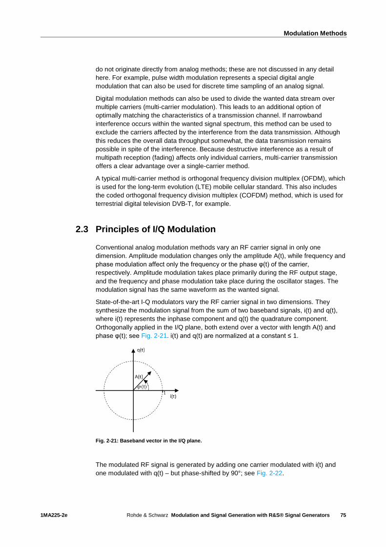
Modulation Methods
1MA225-2e Rohde & Schwarz Modulation and Signal Generation with R&S® Signal Generators
75
do not originate directly from analog methods; these are not discussed in any detail
here. For example, pulse width modulation represents a special digital angle
modulation that can also be used for discrete time sampling of an analog signal.
Digital modulation methods can also be used to divide the wanted data stream over
multiple carriers (multi-carrier modulation). This leads to an additional option of
optimally matching the characteristics of a transmission channel. If narrowband
interference occurs within the wanted signal spectrum, this method can be used to
exclude the carriers affected by the interference from the data transmission. Although
this reduces the overall data throughput somewhat, the data transmission remains
possible in spite of the interference. Because destructive interference as a result of
multipath reception (fading) affects only individual carriers, multi-carrier transmission
offers a clear advantage over a single-carrier method.
A typical multi-carrier method is orthogonal frequency division multiplex (OFDM), which
is used for the long-term evolution (LTE) mobile cellular standard. This also includes
the coded orthogonal frequency division multiplex (COFDM) method, which is used for
terrestrial digital television DVB-T, for example.
2.3 Principles of I/Q Modulation
Conventional analog modulation methods vary an RF carrier signal in only one
dimension. Amplitude modulation changes only the amplitude A(t), while frequency and
phase modulation affect only the frequency or the phase φ(t) of the carrier,
respectively. Amplitude modulation takes place primarily during the RF output stage,
and the frequency and phase modulation take place during the oscillator stages. The
modulation signal has the same waveform as the wanted signal.
State-of-the-art I-Q modulators vary the RF carrier signal in two dimensions. They
synthesize the modulation signal from the sum of two baseband signals, i(t) and q(t),
where i(t) represents the inphase component and q(t) the quadrature component.
Orthogonally applied in the I/Q plane, both extend over a vector with length A(t) and
phase φ(t); see Fig. 2-21. i(t) and q(t) are normalized at a constant ≤ 1.
Fig. 2-21: Baseband vector in the I/Q plane.
The modulated RF signal is generated by adding one carrier modulated with i(t) and
one modulated with q(t) – but phase-shifted by 90°; see Fig. 2-22.

Modulation Methods
1MA225-2e Rohde & Schwarz Modulation and Signal Generation with R&S® Signal Generators
76
Fig. 2-22: Upconversion of the baseband signals.
By using two baseband signals, it is possible to determine the magnitude as well as the
phase of the modulated signal at any given point in time. This also makes it fairly easy
to implement analog modulation.
Amplitude modulation is performed by varying the length of the vector φ(t) versus time
without changing the phase. Frequency modulation and phase modulation involve
varying the phase φ(t) of the sum vector without changing the amplitude (see also I-Q
Modulator, section 1.2.2.1).
Constellation diagram
The constellation diagram provides a graphical representation of the in-phase and
quadrature-phase components of the digitally modulated signal. This displays a vector
in a Cartesian system of coordinates, along with the amplitude and phase of a given
carrier at the sampling point in time. Because the symbols to be transmitted represent
complex numbers, they can be displayed as points in the constellation diagram, which
corresponds to the complex plane. These points in turn correspond to the terminals of
the respective I/Q vectors.
Fig. 2-23 shows the constellation diagram for binary phase shift keying (BPSK) and for
4-PSK (see section 2.4.3 ). As can also be seen here, the included I/Q states are in a
steady state only at the symbol points in time. Of course, transitions occur between
those points in time.
Fig. 2-23: Constellation diagram for BPSK (left) and 4-PSK (right).
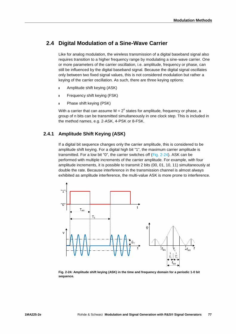
Modulation Methods
1MA225-2e Rohde & Schwarz Modulation and Signal Generation with R&S® Signal Generators
77
2.4 Digital Modulation of a Sine-Wave Carrier
Like for analog modulation, the wireless transmission of a digital baseband signal also
requires transition to a higher frequency range by modulating a sine-wave carrier. One
or more parameters of the carrier oscillation, i.e. amplitude, frequency or phase, can
still be influenced by the digital baseband signal. Because the digital signal oscillates
only between two fixed signal values, this is not considered modulation but rather a
keying of the carrier oscillation. As such, there are three keying options:
ı Amplitude shift keying (ASK)
ı Frequency shift keying (FSK)
ı Phase shift keying (PSK)
With a carrier that can assume M = 2n states for amplitude, frequency or phase, a
group of n bits can be transmitted simultaneously in one clock step. This is included in
the method names, e.g. 2-ASK, 4-PSK or 8-FSK.
2.4.1 Amplitude Shift Keying (ASK)
If a digital bit sequence changes only the carrier amplitude, this is considered to be
amplitude shift keying. For a digital high bit "1", the maximum carrier amplitude is
transmitted. For a low bit "0", the carrier switches off (Fig. 2-24). ASK can be
performed with multiple increments of the carrier amplitude. For example, with four
amplitude increments, it is possible to transmit 2 bits (00, 01, 10, 11) simultaneously at
double the rate. Because interference in the transmission channel is almost always
exhibited as amplitude interference, the multi-value ASK is more prone to interference.
Fig. 2-24: Amplitude shift keying (ASK) in the time and frequency domain for a periodic 1-0 bit
sequence.
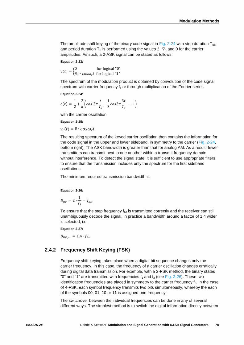
Modulation Methods
1MA225-2e Rohde & Schwarz Modulation and Signal Generation with R&S® Signal Generators
78
The amplitude shift keying of the binary code signal in Fig. 2-24 with step duration TBit
and period duration TS is performed using the values 2 ∙ v𝑐 and 0 for the carrier
amplitudes. As such, a 2-ASK signal can be stated as follows:
Equation 2-23:
v(𝑡) = 0 for logical "0"v𝑇 ∙ 𝑐𝑜𝑠𝜔𝑐𝑡 for logical "1"
The spectrum of the modulation product is obtained by convolution of the code signal
spectrum with carrier frequency fc or through multiplication of the Fourier series
Equation 2-24:
𝑐(𝑡) = 1
2+
2
𝜋(𝑐𝑜𝑠 2𝜋
𝑡
𝑇𝑆
−1
3𝑐𝑜𝑠2𝜋
3𝑡
𝑇𝑆
+ ⋯ )
with the carrier oscillation
Equation 2-25:
v𝑐(𝑡) = v ∙ 𝑐𝑜𝑠𝜔𝑐𝑡
The resulting spectrum of the keyed carrier oscillation then contains the information for
the code signal in the upper and lower sideband, in symmetry to the carrier (Fig. 2-24,
bottom right). The ASK bandwidth is greater than that for analog AM. As a result, fewer
transmitters can transmit next to one another within a transmit frequency domain
without interference. To detect the signal state, it is sufficient to use appropriate filters
to ensure that the transmission includes only the spectrum for the first sideband
oscillations.
The minimum required transmission bandwidth is:
Equation 2-26:
𝐵𝐻𝐹 = 2 ∙1
𝑇𝑆
= 𝑓𝐵𝑖𝑡
To ensure that the step frequency fbit is transmitted correctly and the receiver can still
unambiguously decode the signal, in practice a bandwidth around a factor of 1.4 wider
is selected, i.e.
Equation 2-27:
𝐵𝐻𝐹,𝑝𝑟 = 1.4 ∙ 𝑓𝐵𝑖𝑡
2.4.2 Frequency Shift Keying (FSK)
Frequency shift keying takes place when a digital bit sequence changes only the
carrier frequency. In this case, the frequency of a carrier oscillation changes erratically
during digital data transmission. For example, with a 2-FSK method, the binary states
"0" and "1" are transmitted with frequencies f1 and f2 (see Fig. 2-26). These two
identification frequencies are placed in symmetry to the carrier frequency fc. In the case
of 4-FSK, each symbol frequency transmits two bits simultaneously, whereby the each
of the symbols 00, 01, 10 or 11 is assigned one frequency.
The switchover between the individual frequencies can be done in any of several
different ways. The simplest method is to switch the digital information directly between
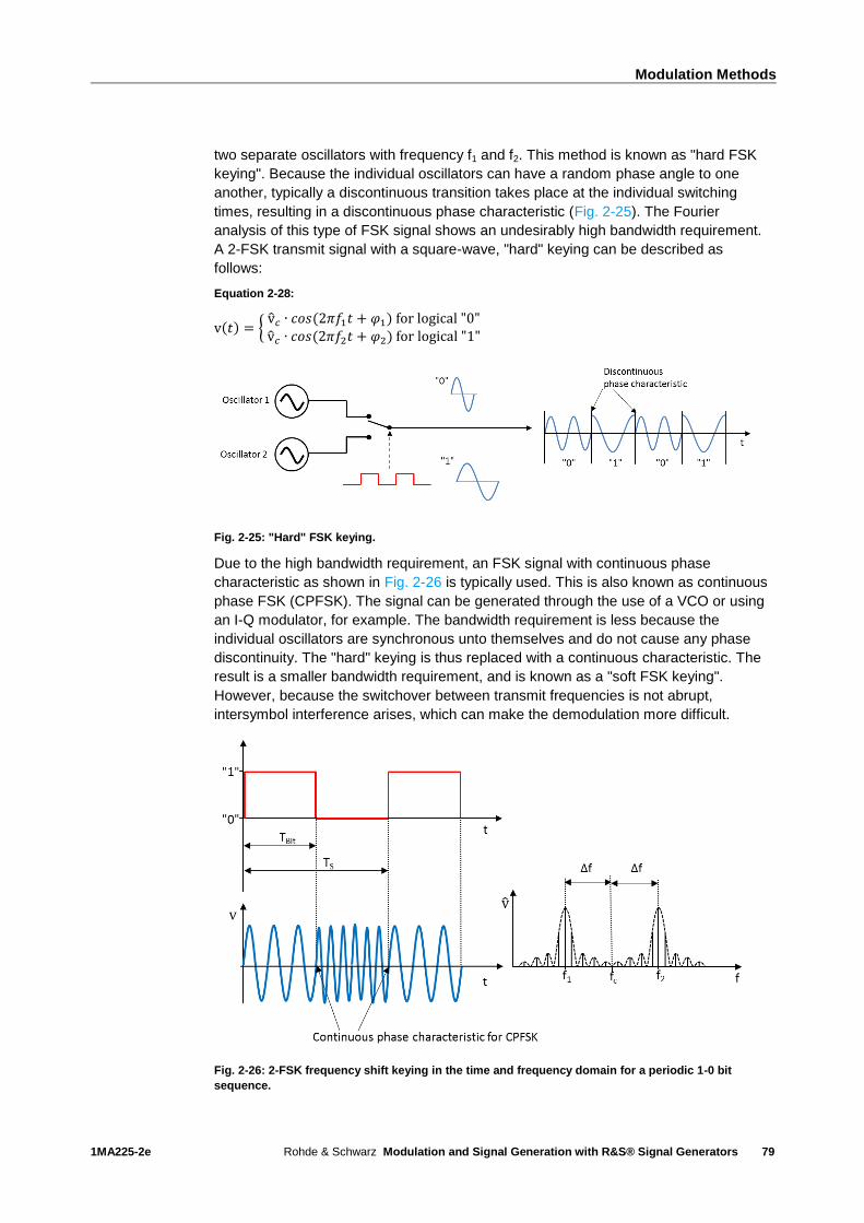
Modulation Methods
1MA225-2e Rohde & Schwarz Modulation and Signal Generation with R&S® Signal Generators
79
two separate oscillators with frequency f1 and f2. This method is known as "hard FSK
keying". Because the individual oscillators can have a random phase angle to one
another, typically a discontinuous transition takes place at the individual switching
times, resulting in a discontinuous phase characteristic (Fig. 2-25). The Fourier
analysis of this type of FSK signal shows an undesirably high bandwidth requirement.
A 2-FSK transmit signal with a square-wave, "hard" keying can be described as
follows:
Equation 2-28:
v(𝑡) = v𝑐 ∙ 𝑐𝑜𝑠(2𝜋𝑓1𝑡 + 𝜑1) for logical "0"v𝑐 ∙ 𝑐𝑜𝑠(2𝜋𝑓2𝑡 + 𝜑2) for logical "1"
Fig. 2-25: "Hard" FSK keying.
Due to the high bandwidth requirement, an FSK signal with continuous phase
characteristic as shown in Fig. 2-26 is typically used. This is also known as continuous
phase FSK (CPFSK). The signal can be generated through the use of a VCO or using
an I-Q modulator, for example. The bandwidth requirement is less because the
individual oscillators are synchronous unto themselves and do not cause any phase
discontinuity. The "hard" keying is thus replaced with a continuous characteristic. The
result is a smaller bandwidth requirement, and is known as a "soft FSK keying".
However, because the switchover between transmit frequencies is not abrupt,
intersymbol interference arises, which can make the demodulation more difficult.
Fig. 2-26: 2-FSK frequency shift keying in the time and frequency domain for a periodic 1-0 bit
sequence.

Modulation Methods
1MA225-2e Rohde & Schwarz Modulation and Signal Generation with R&S® Signal Generators
80
A 2-FSK signal can also be seen as the superposition of two amplitude-keyed
oscillations with the frequencies f1 and f2. This translates into the spectrum based on a
superposition of the spectra of the two ASK signals. The required bandwidth for a
2-FSK signal depends on the frequency deviation ∆f or on the frequency difference
ǀf1-f2ǀ = 2∙∆f . For 2 ∙ ∆𝑓 >>1
𝑇𝐵𝑖𝑡, with a periodic 1-0 bit sequence, the result is a
symmetrical spectrum as shown in Fig. 2-26, bottom right. If the distribution is unequal,
the spectrum will be asymmetrical. For 2 ∙ ∆𝑓 >1
𝑇𝐵𝑖𝑡, the following bandwidth can be
approximated:
Equation 2-29:
𝐵𝐻𝐹 = 2 ∙ (∆𝑓 + 𝐵)
where: B = Bandwidth of the baseband signal
The modulation index m for FSK is the product of the overall frequency deviation
(2 ∙ ∆𝑓) and the duration TBit of a symbol:
Equation 2-30:
m = 2 ∙ ∆𝑓 ∙ 𝑇𝐵𝑖𝑡
Like for analog FM, the frequency deviation ∆𝑓 is defined as the maximum deviation of
the instantaneous frequency from the carrier frequency fc. As seen in Equation 2-30,
the modulation index decreases as the offset for the two frequencies f1 and f2 is
reduced at a constant symbol rate. The smallest possible value of m that still permits
an orthogonal FSK is 0.5. It is only with an orthogonal FSK and an integer multiplier of
m = 0.5 that the intersymbol interference between two individual symbols remains at a
minimum, with the result that the mutual influence is also minimal. The method that
uses m = 0.5 is known as minimum shift keying (MSK), or fast frequency shift keying
(FFSK). For MSK, ∆𝑓 between binary "1" and "0" is exactly one half the data rate.
Fig. 2-27: Relationship between data signal, frequency, and phase for MSK.
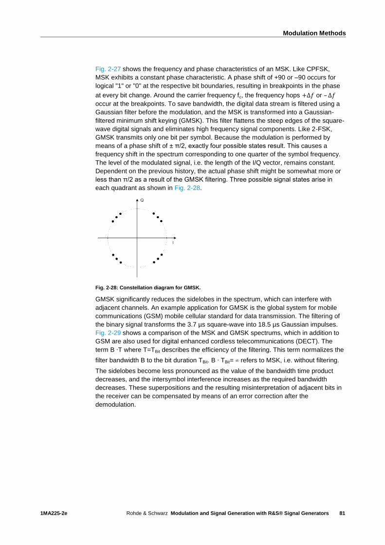
Modulation Methods
1MA225-2e Rohde & Schwarz Modulation and Signal Generation with R&S® Signal Generators
81
Fig. 2-27 shows the frequency and phase characteristics of an MSK. Like CPFSK,
MSK exhibits a constant phase characteristic. A phase shift of +90 or –90 occurs for
logical "1" or "0" at the respective bit boundaries, resulting in breakpoints in the phase
at every bit change. Around the carrier frequency fc, the frequency hops +∆𝑓 or – ∆𝑓
occur at the breakpoints. To save bandwidth, the digital data stream is filtered using a
Gaussian filter before the modulation, and the MSK is transformed into a Gaussian-
filtered minimum shift keying (GMSK). This filter flattens the steep edges of the square-
wave digital signals and eliminates high frequency signal components. Like 2-FSK,
GMSK transmits only one bit per symbol. Because the modulation is performed by
means of a phase shift of ± π/2, exactly four possible states result. This causes a
frequency shift in the spectrum corresponding to one quarter of the symbol frequency.
The level of the modulated signal, i.e. the length of the I/Q vector, remains constant.
Dependent on the previous history, the actual phase shift might be somewhat more or
less than π/2 as a result of the GMSK filtering. Three possible signal states arise in
each quadrant as shown in Fig. 2-28.
Fig. 2-28: Constellation diagram for GMSK.
GMSK significantly reduces the sidelobes in the spectrum, which can interfere with
adjacent channels. An example application for GMSK is the global system for mobile
communications (GSM) mobile cellular standard for data transmission. The filtering of
the binary signal transforms the 3.7 µs square-wave into 18.5 µs Gaussian impulses.
Fig. 2-29 shows a comparison of the MSK and GMSK spectrums, which in addition to
GSM are also used for digital enhanced cordless telecommunications (DECT). The
term B ∙T where T=TBit describes the efficiency of the filtering. This term normalizes the
filter bandwidth B to the bit duration TBit. B ∙ TBit= ∞ refers to MSK, i.e. without filtering.
The sidelobes become less pronounced as the value of the bandwidth time product
decreases, and the intersymbol interference increases as the required bandwidth
decreases. These superpositions and the resulting misinterpretation of adjacent bits in
the receiver can be compensated by means of an error correction after the
demodulation.
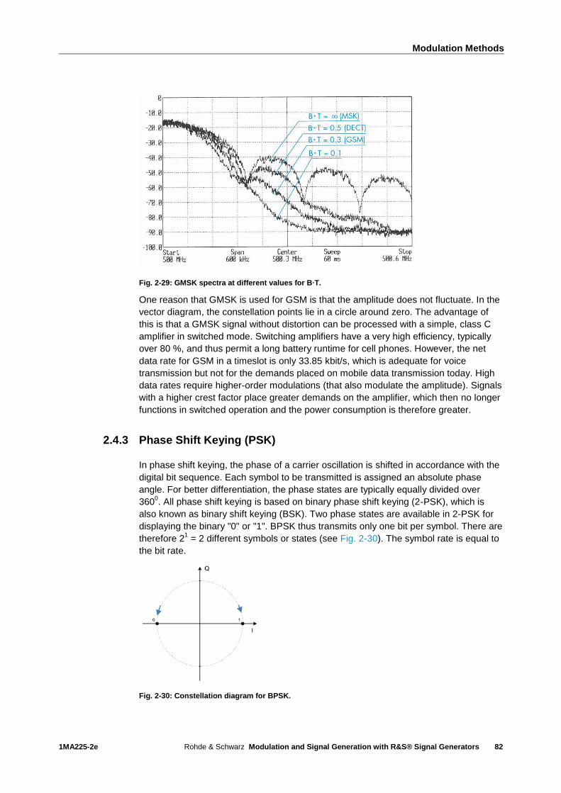
Modulation Methods
1MA225-2e Rohde & Schwarz Modulation and Signal Generation with R&S® Signal Generators
82
Fig. 2-29: GMSK spectra at different values for B∙T.
One reason that GMSK is used for GSM is that the amplitude does not fluctuate. In the
vector diagram, the constellation points lie in a circle around zero. The advantage of
this is that a GMSK signal without distortion can be processed with a simple, class C
amplifier in switched mode. Switching amplifiers have a very high efficiency, typically
over 80 %, and thus permit a long battery runtime for cell phones. However, the net
data rate for GSM in a timeslot is only 33.85 kbit/s, which is adequate for voice
transmission but not for the demands placed on mobile data transmission today. High
data rates require higher-order modulations (that also modulate the amplitude). Signals
with a higher crest factor place greater demands on the amplifier, which then no longer
functions in switched operation and the power consumption is therefore greater.
2.4.3 Phase Shift Keying (PSK)
In phase shift keying, the phase of a carrier oscillation is shifted in accordance with the
digital bit sequence. Each symbol to be transmitted is assigned an absolute phase
angle. For better differentiation, the phase states are typically equally divided over
3600. All phase shift keying is based on binary phase shift keying (2-PSK), which is
also known as binary shift keying (BSK). Two phase states are available in 2-PSK for
displaying the binary "0" or "1". BPSK thus transmits only one bit per symbol. There are
therefore 21 = 2 different symbols or states (see Fig. 2-30). The symbol rate is equal to
the bit rate.
Fig. 2-30: Constellation diagram for BPSK.
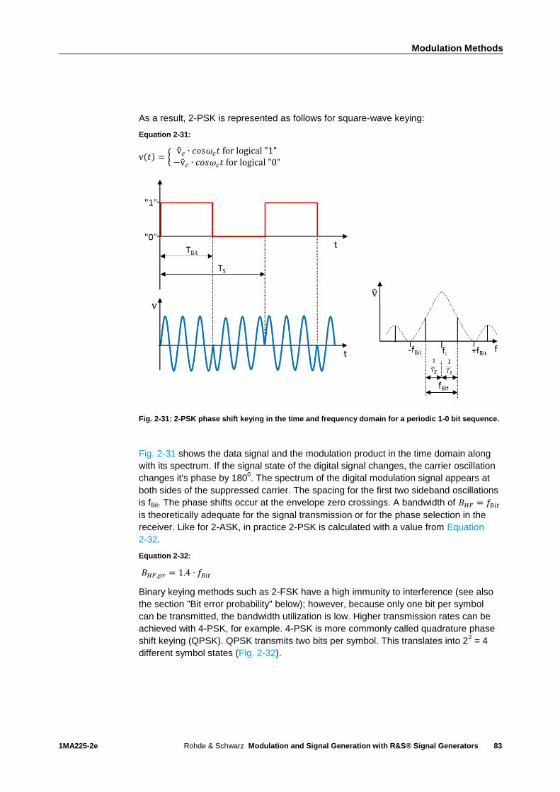
Modulation Methods
1MA225-2e Rohde & Schwarz Modulation and Signal Generation with R&S® Signal Generators
83
As a result, 2-PSK is represented as follows for square-wave keying:
Equation 2-31:
v(𝑡) = v𝑐 ∙ 𝑐𝑜𝑠𝜔𝑐𝑡 for logical "1"
−v𝑐 ∙ 𝑐𝑜𝑠𝜔𝑐𝑡 for logical "0"
Fig. 2-31: 2-PSK phase shift keying in the time and frequency domain for a periodic 1-0 bit sequence.
Fig. 2-31 shows the data signal and the modulation product in the time domain along
with its spectrum. If the signal state of the digital signal changes, the carrier oscillation
changes it's phase by 1800. The spectrum of the digital modulation signal appears at
both sides of the suppressed carrier. The spacing for the first two sideband oscillations
is fBit. The phase shifts occur at the envelope zero crossings. A bandwidth of 𝐵𝐻𝐹 = 𝑓𝐵𝑖𝑡
is theoretically adequate for the signal transmission or for the phase selection in the
receiver. Like for 2-ASK, in practice 2-PSK is calculated with a value from Equation
2-32.
Equation 2-32:
𝐵𝐻𝐹,𝑝𝑟 = 1.4 ∙ 𝑓𝐵𝑖𝑡
Binary keying methods such as 2-FSK have a high immunity to interference (see also
the section "Bit error probability" below); however, because only one bit per symbol
can be transmitted, the bandwidth utilization is low. Higher transmission rates can be
achieved with 4-PSK, for example. 4-PSK is more commonly called quadrature phase
shift keying (QPSK). QPSK transmits two bits per symbol. This translates into 22 = 4
different symbol states (Fig. 2-32).
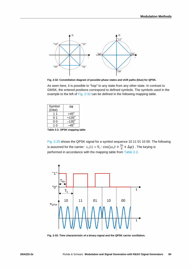
Modulation Methods
1MA225-2e Rohde & Schwarz Modulation and Signal Generation with R&S® Signal Generators
84
Fig. 2-32: Constellation diagram of possible phase states and shift paths (blue) for QPSK.
As seen here, it is possible to "hop" to any state from any other state. In contrast to
GMSK, the entered positions correspond to defined symbols. The symbols used in the
example to the left of Fig. 2-32 can be defined in the following mapping table.
Symbol (Dibit)
∆φ
1 1 +45o
0 1 +135o
0 0 –1350
1 0 –450
Table 2-2: OPSK mapping table
Fig. 2-33 shows the QPSK signal for a symbol sequence 10 11 01 10 00. The following
is assumed for the carrier: v𝑐(𝑡) = v𝑐 ∙ cos (𝜔𝑐𝑡 + 3𝜋
4+ ∆𝜑) . The keying is
performed in accordance with the mapping table from Table 2-2.
Fig. 2-33: Time characteristic of a binary signal and the QPSK carrier oscillation.
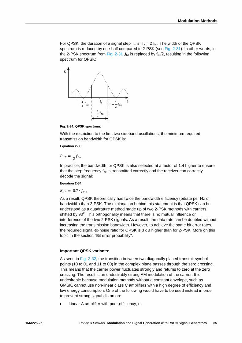
Modulation Methods
1MA225-2e Rohde & Schwarz Modulation and Signal Generation with R&S® Signal Generators
85
For QPSK, the duration of a signal step Ts is: Ts = 2Tbit. The width of the QPSK
spectrum is reduced by one-half compared to 2-PSK (see Fig. 2-31). In other words, in
the 2-PSK spectrum from Fig. 2-31 ,fbit is replaced by fbit/2, resulting in the following
spectrum for QPSK:
Fig. 2-34: QPSK spectrum.
With the restriction to the first two sideband oscillations, the minimum required
transmission bandwidth for QPSK is:
Equation 2-33:
𝐵𝐻𝐹 = 1
2𝑓𝐵𝑖𝑡
In practice, the bandwidth for QPSK is also selected at a factor of 1.4 higher to ensure
that the step frequency fbit is transmitted correctly and the receiver can correctly
decode the signal:
Equation 2-34:
𝐵𝐻𝐹 = 0.7 ∙ 𝑓𝐵𝑖𝑡
As a result, QPSK theoretically has twice the bandwidth efficiency (bitrate per Hz of
bandwidth) than 2-PSK. The explanation behind this statement is that QPSK can be
understood as a quadrature method made up of two 2-PSK methods with carriers
shifted by 90o. This orthogonality means that there is no mutual influence or
interference of the two 2-PSK signals. As a result, the data rate can be doubled without
increasing the transmission bandwidth. However, to achieve the same bit error rates,
the required signal-to-noise ratio for QPSK is 3 dB higher than for 2-PSK. More on this
topic in the section "Bit error probability".
Important QPSK variants:
As seen in Fig. 2-32, the transition between two diagonally placed transmit symbol
points (10 to 01 and 11 to 00) in the complex plane passes through the zero crossing.
This means that the carrier power fluctuates strongly and returns to zero at the zero
crossing. The result is an undesirably strong AM modulation of the carrier. It is
undesirable because modulation methods without a constant envelope, such as
GMSK, cannot use non-linear class C amplifiers with a high degree of efficiency and
low energy consumption. One of the following would have to be used instead in order
to prevent strong signal distortion:
ı Linear A amplifier with poor efficiency, or

Modulation Methods
1MA225-2e Rohde & Schwarz Modulation and Signal Generation with R&S® Signal Generators
86
ı CPU-intensive signal predistortion of the amplifier characteristics
As seen in Fig. 2-34, the spectral line for carrier frequency fc is missing from the
spectrum in QPSK modulation, or in any phase-modulated RF carrier for that matter.
As a result, the current phase angle is not referenced to the phase of the unmodulated
carrier. The zero crossings in QPSK make it more difficult to restore the carrier for a
coherent demodulation, by which is meant the exact reconstruction of the carrier
frequency with the associated phase angle.
This problem can be alleviated with π/4-DQPSK modulation. Independent of the user
data, an additional phase shift of π/4 (45°) is performed after each transmit symbol.
This ensures that the transition between two symbols never transverses the origin and
always only one carrier amplitude is transmitted (see Fig. 2-35).
Fig. 2-35: 𝝅
𝟒 DQPSK for preventing zero crossings.
In addition, information is not transmitted regarding the current phase angle, but rather
regarding the difference to the previous phase angle. Hence the name differential
quadrature phase shift keying (π/4-DQPSK). The biggest advantage of this method is
that no coherent demodulation is needed, eliminating the complex reconstruction of the
carrier. In addition, the clock synchronization on the receiver end is made easier
because regular phase shifts are present in the receive signal, independent of the user
data and its coding. Table 2-3 lists the permissible phase states for π/4-DQPSK. This
shows that π/4-DQPSK allows only 45o and 135
o phase rotations.
Symbol (Dibit)
Phase transition ∆φ
0 0 0 ∙ π/2 + π/4 = 45o
0 1 1 ∙ π/2 + π/4 = 3π/4 = 135o
1 1 2 ∙ π/2 + π/4 = 5π/4 = 225o = –135
o
1 0 3 ∙ π/2 + π/4 = 7π/4 = 315o = –45
o
Table 2-3: Allowed phase states for π/4-DQPSK
Another option for preventing zero crossings and the associated reduction in amplitude
is offered by offset QPSK (OQPSK). To achieve this, the maximum phase change for
OQPSK is only 90o instead of the 180
o for conventional QPSK. With QPSK, the two bit
streams used to generate the I and Q signals are synchronous, i.e. their sign changes
occur simultaneously. If both binary signals change state at the same time in QPSK, a

Modulation Methods
1MA225-2e Rohde & Schwarz Modulation and Signal Generation with R&S® Signal Generators
87
phase shift of 180o occurs. In the case of OQPSK, the two data streams are shifted
toward one another at half a step length of TS or at a bit time of TBit and then applied to
the modulators for I and Q (Fig. 2-36), ensuring that they no longer change
simultaneously.
Fig. 2-36: Generating an offset QPSK.
As a result, only one of the two modulators will undergo a phase change at the same
time as a bit change. 180o phase shifts are therefore eliminated, and instead are split
into two shifts of 90o each. An example is provided in Fig. 2-37.
Fig. 2-37: Phase characteristic of QPSK and OQPSK over time.
In contrast to true QPSK, state transitions for OQPSK form a square defined by the
four states. This prevents diagonal paths with a zero crossing (Fig. 2-38).
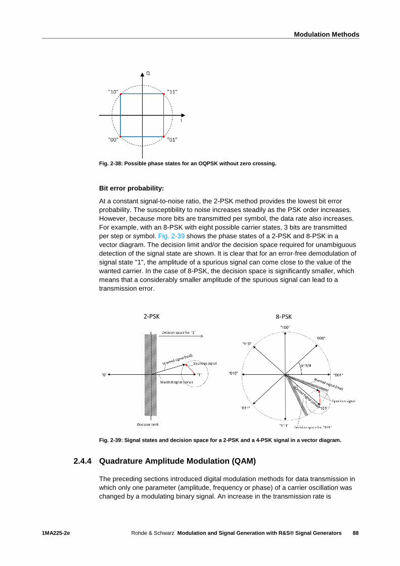
Modulation Methods
1MA225-2e Rohde & Schwarz Modulation and Signal Generation with R&S® Signal Generators
88
Fig. 2-38: Possible phase states for an OQPSK without zero crossing.
Bit error probability:
At a constant signal-to-noise ratio, the 2-PSK method provides the lowest bit error
probability. The susceptibility to noise increases steadily as the PSK order increases.
However, because more bits are transmitted per symbol, the data rate also increases.
For example, with an 8-PSK with eight possible carrier states, 3 bits are transmitted
per step or symbol. Fig. 2-39 shows the phase states of a 2-PSK and 8-PSK in a
vector diagram. The decision limit and/or the decision space required for unambiguous
detection of the signal state are shown. It is clear that for an error-free demodulation of
signal state "1", the amplitude of a spurious signal can come close to the value of the
wanted carrier. In the case of 8-PSK, the decision space is significantly smaller, which
means that a considerably smaller amplitude of the spurious signal can lead to a
transmission error.
Fig. 2-39: Signal states and decision space for a 2-PSK and a 4-PSK signal in a vector diagram.
2.4.4 Quadrature Amplitude Modulation (QAM)
The preceding sections introduced digital modulation methods for data transmission in
which only one parameter (amplitude, frequency or phase) of a carrier oscillation was
changed by a modulating binary signal. An increase in the transmission rate is

Modulation Methods
1MA225-2e Rohde & Schwarz Modulation and Signal Generation with R&S® Signal Generators
89
achieved by modulating the amplitude and phase of a high-frequency carrier. The
method that combines amplitude and phase modulation is known as quadrature
amplitude modulation (QAM). While the signal states lie in a circle for PSK, this is no
longer the case when the amplitude is changed. The only exception is 4-QAM, which is
identical to 4-PSK/QPSK (see Fig. 2-40, left). Fig. 2-40 (right) shows the signal states
for 16-QAM as an example. Four bits are transmitted per symbol. The result is 24 = 16
symbols. The symbol rate is ¼ the bit rate. This symbol placement in the constellation
diagram includes three different amplitudes, one with eight different phase values and
two with four phase values.
Fig. 2-40: Constellation diagram for 4-QAM or 4-PSK (QPSK) on the left and for 16-QAM on the right.
Fig. 2-41 shows another example of the symbol placement for 16-QAM. This diagram
includes four different values for amplitude, each with four values for phase.
Fig. 2-41: 16-QAM with four amplitudes, each with four different phases.
A QAM requires less power than PSK at the same weighting M and the same bit error
probability. The following general statement applies for a QAM signal:
Equation 2-35:
v(𝑡) = 𝐼(𝑡) ∙ 𝑐𝑜𝑠𝜔𝑐𝑡 − 𝑄(𝑡) ∙ sin 𝜔𝑐𝑡
where 𝜔𝑐 = 2𝜋𝑓𝑐
The following applies for the complex envelope of the QAM signal:
Equation 2-36:
v(𝑡) = 𝐼(𝑡) + 𝑗𝑄(𝑡) = v𝑐(𝑡) ∙ 𝑒𝑗𝜑(𝑡)
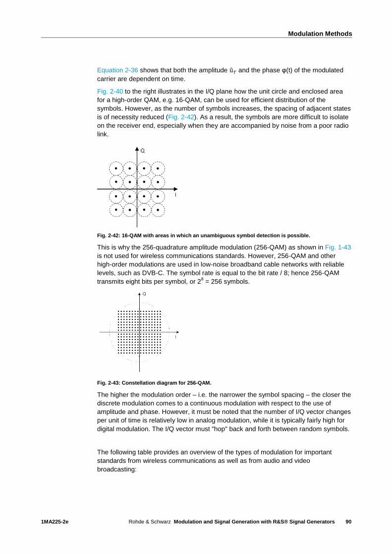
Modulation Methods
1MA225-2e Rohde & Schwarz Modulation and Signal Generation with R&S® Signal Generators
90
Equation 2-36 shows that both the amplitude u𝑇 and the phase φ(t) of the modulated
carrier are dependent on time.
Fig. 2-40 to the right illustrates in the I/Q plane how the unit circle and enclosed area
for a high-order QAM, e.g. 16-QAM, can be used for efficient distribution of the
symbols. However, as the number of symbols increases, the spacing of adjacent states
is of necessity reduced (Fig. 2-42). As a result, the symbols are more difficult to isolate
on the receiver end, especially when they are accompanied by noise from a poor radio
link.
Fig. 2-42: 16-QAM with areas in which an unambiguous symbol detection is possible.
This is why the 256-quadrature amplitude modulation (256-QAM) as shown in Fig. 1-43
is not used for wireless communications standards. However, 256-QAM and other
high-order modulations are used in low-noise broadband cable networks with reliable
levels, such as DVB-C. The symbol rate is equal to the bit rate / 8; hence 256-QAM
transmits eight bits per symbol, or 28 = 256 symbols.
Fig. 2-43: Constellation diagram for 256-QAM.
The higher the modulation order – i.e. the narrower the symbol spacing – the closer the
discrete modulation comes to a continuous modulation with respect to the use of
amplitude and phase. However, it must be noted that the number of I/Q vector changes
per unit of time is relatively low in analog modulation, while it is typically fairly high for
digital modulation. The I/Q vector must "hop" back and forth between random symbols.
The following table provides an overview of the types of modulation for important
standards from wireless communications as well as from audio and video
broadcasting:
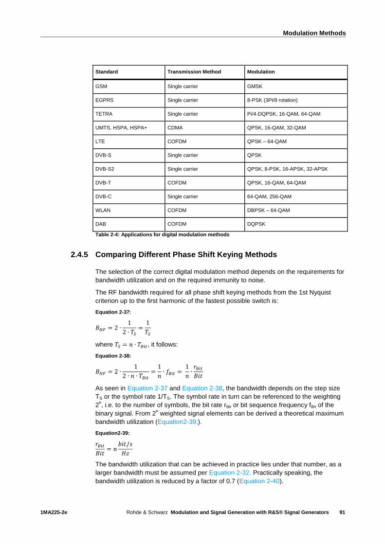
Modulation Methods
1MA225-2e Rohde & Schwarz Modulation and Signal Generation with R&S® Signal Generators
91
Standard Transmission Method Modulation
GSM Single carrier GMSK
EGPRS Single carrier 8-PSK (3Pi/8 rotation)
TETRA Single carrier Pi/4-DQPSK, 16-QAM, 64-QAM
UMTS, HSPA, HSPA+ CDMA QPSK, 16-QAM, 32-QAM
LTE COFDM QPSK – 64-QAM
DVB-S Single carrier QPSK
DVB-S2 Single carrier QPSK, 8-PSK, 16-APSK, 32-APSK
DVB-T COFDM QPSK, 16-QAM, 64-QAM
DVB-C Single carrier 64-QAM, 256-QAM
WLAN COFDM DBPSK – 64-QAM
DAB COFDM DQPSK
Table 2-4: Applications for digital modulation methods
2.4.5 Comparing Different Phase Shift Keying Methods
The selection of the correct digital modulation method depends on the requirements for
bandwidth utilization and on the required immunity to noise.
The RF bandwidth required for all phase shift keying methods from the 1st Nyquist
criterion up to the first harmonic of the fastest possible switch is:
Equation 2-37:
𝐵𝐻𝐹 = 2 ∙1
2 ∙ 𝑇𝑆
=1
𝑇𝑆
where 𝑇𝑆 = 𝑛 ∙ 𝑇𝐵𝑖𝑡, it follows:
Equation 2-38:
𝐵𝐻𝐹 = 2 ∙1
2 ∙ 𝑛 ∙ 𝑇𝐵𝑖𝑡
=1
𝑛∙ 𝑓𝐵𝑖𝑡 =
1
𝑛∙
𝑟𝐵𝑖𝑡
𝐵𝑖𝑡
As seen in Equation 2-37 and Equation 2-38, the bandwidth depends on the step size
TS or the symbol rate 1/TS. The symbol rate in turn can be referenced to the weighting
2n, i.e. to the number of symbols, the bit rate rBit or bit sequence frequency fBit of the
binary signal. From 2n weighted signal elements can be derived a theoretical maximum
bandwidth utilization (Equation2-39:).
Equation2-39:
𝑟𝐵𝑖𝑡
𝐵𝑖𝑡= 𝑛
𝑏𝑖𝑡/𝑠
𝐻𝑧
The bandwidth utilization that can be achieved in practice lies under that number, as a
larger bandwidth must be assumed per Equation 2-32. Practically speaking, the
bandwidth utilization is reduced by a factor of 0.7 (Equation 2-40).

Modulation Methods
1MA225-2e Rohde & Schwarz Modulation and Signal Generation with R&S® Signal Generators
92
Equation 2-40:
𝑟𝐵𝑖𝑡
𝐵𝑖𝑡= 0.7 ∙ 𝑛
𝑏𝑖𝑡/𝑠
𝐻𝑧
The comparison of the variously weighted PSK and QAM methods in Table 2-5 shows
that the bandwidth utilization increases with the weighting of the method, and the
bandwidth can be reduced at the specified bit rate. The table also shows that with an
increasing bandwidth utilization, the signal-to-noise ratio (C/N) must steadily increase
in order not to stay below a defined bit error rate (BER).
Modulation 2-PSK 4-PSK 8-PSK 16-PSK 16-QAM 32-QAM 64-QAM
Amplitude states 1 1 1 1 3 5 9
Phase states 2 4 8 16 12 28 52
Carrier states 2 4 8 16 16 32 64
Theoretical maximum bandwidth utilization in (bit/s)/Hz
1 2 3 4 4 5 6
Practical bandwidth utilization in (bit/s)/Hz
0.7 1.4 2.1 2.8 2.8 3.6 4.2
C/N in dB for BER=10–6
, in practice
10.7 13.7 18.8 24 20.5 24 27
Table 2-5: Comparison of different phase shift keying methods
2.4.6 Crest Factor / Linearity Requirements
The amplitude of the modulated RF transmit signal is always proportionate to the
corresponding vector length in the baseband – including between the symbol points in
time. When considered in this light, it is clear that the unit circle is frequently violated
by the transitions between the symbols. The ratio of peak value to average value is
called the crest factor. It determines the power margin that must be reserved at the TX
output stage.
Similarly, Fig. 2-44 shows signal breaks that pass through the origin and then return to
zero. For an error-free demodulation on the receiver end, it is important that the signal
characteristic be transmitted totally without distortion. The transmit output stage must
therefore not only maintain some headroom for high power levels, but must also exhibit
very high linearity over the entire power range from 0 watts to the maximum power.
Fig. 2-44: Constellation and continuous vector diagram.
GSM primarily uses the two modulation methods GMSK and 8-PSK. In GMSK, the
ideal I/Q vector remains exclusively on the unit circle. Theoretically there are no power
peaks or amplitude notches, and no crest factors of 1.

Modulation Methods
1MA225-2e Rohde & Schwarz Modulation and Signal Generation with R&S® Signal Generators
93
With 8-PSK, the zero crossings required during hops between opposing symbols in the
I/Q diagram are avoided by rotating the constellation diagram by 3π/8 between the
symbol clocks. The vector diagram in Fig. 2-45 shows the desired effect, which has no
zero crossings. The transmit power in Fig. 2-46 shows level breaks of about 12 dB
during data transmission, but not down to zero. This somewhat moderates the linearity
requirements for the TX output stage.
As a result of the rotation, about 16 symbol states will be recalculated at the receiver
end during demodulation.
Fig. 2-45: Preventing zero crossings by rotating the constellation.
Fig. 2-46: Progression of the envelope power for a 3π/8 rotated, 8-PSK-modulated signal.
2.5 Access Methods
Digital wireless communications networks are organized into cells. Because radio
waves have a limited range, it is possible to define an area – called a cell – inside of
which service to wireless subscribers is provided by a single base station (BS). At the
reception boundaries, a mobile phone (also called a mobile station, MS or user
equipment, UE) is automatically switched to the adjacent cell that is most suitable
(handover). This typically also involves a change in frequency. The original frequency
might then be available again in the next cell over (frequency reuse).
Because every cell is limited to a specific area, it can handle a finite number of wireless
subscribers. Or, stated conversely: The size of a wireless communications cell is
Modulation Methods
1MA225-2e Rohde & Schwarz Modulation and Signal Generation with R&S® Signal Generators
94
determined primarily by its required capacity. Because the available resources of
frequency, time and – as we will see later – code are limited, locations with a large
potential number of subscribers must have many base stations with correspondingly
low power. Regions with fewer subscribers can have large cells with powerful base
stations. The point is to ensure that multiple subscribers have access to a fixed
percentage of the resources frequency, time and code – independent of the uplink /
downlink duplex.
Three different methods are used most frequently:
ı Frequency-division multiple access (FDMA)
ı Time-division multiple access (TDMA)
ı Code-division multiple access (CDMA)
Modern vector signal generators are able to offer these methods for standard-
compliant generation of signals.
Fig. 2-47 illustrates the primary differences. This simplification assumes only five
subscribers (each represented by a different color), all with equal power. This is
seldom the case in practice, but it is sufficient for understanding the differences.
Fig. 2-47: Three important access methods.
FDMA divides the wireless subscribers in a cell among different frequencies. Fig. 2-47
shows five subscribers allocated to five frequencies. For FDD, this means five
frequency pairs. FDMA is very easy to implement. This method is particularly useful in
small cells where the allocated frequencies can be reused a short distance away.
FDMA is frequently used in combination with TDD, e.g. for DECT1 and WLAN
2 (both
standards specialize in connections over short distances).
1 Digital enhanced cordless telecommunications
2 Wireless local area network

Exercises
1MA225-2e Rohde & Schwarz Modulation and Signal Generation with R&S® Signal Generators
95
3 Exercises
3.1 Amplitude Modulation
Amplitude modulation is one of the oldest modulation methods. Even if this type of
modulation plays a lesser role in today's world, amplitude-modulated signals represent
a very good way of understanding modulation fundamentals.
The objective of this lab exercise is to generate amplitude-modulated signals and to
observe and measure variable modulation parameters. It will also provide a feel for the
various signal waveforms in the time and spectral domain.
3.1.1 Test Setup
In order to generate and measure modulation signals, you will need a generator, a
signal analyzer and an oscilloscope as shown in Fig. 3-1. The oscilloscope is used to
measure the modulation signal at the same times as it measures the unmodulated
wanted signal.
Fig. 3-1: Hardware setup for measuring AM signals.

Exercises
1MA225-2e Rohde & Schwarz Modulation and Signal Generation with R&S® Signal Generators
96
3.1.2 Measurement
Set up the signal generator as follows: Carrier frequency 100 kHz Signal frequency 1 kHz Amplitude 0 dBm Modulation depth any LF Gen Shape Sine
These settings are made in "RF/A Mod" > "Amplitude Modulation"; see Fig. 3-2.
Fig. 3-2: Configuring the generator.
To display the wanted signal on the oscilloscope, switch on the LF generator output on
the SMBV.
Under "RF/A Mod" > "LF Generator / Output", set the "LF Output State" option to
ON and set the level to 500 mV; see Fig. 3-3.
Fig. 3-3: Configuring the LF generator.
Make the appropriate settings on the oscilloscope.
On the screen, at least two periods of the wanted signal should be clearly visible along with the modulated and the original signal. Verify both signals, taking special note of the phase angle.
Change the modulation depth and other parameters and observe the effects on the time domain signal.
Exercises
1MA225-2e Rohde & Schwarz Modulation and Signal Generation with R&S® Signal Generators
97
Measurements in the time domain
In the time domain, the modulation depth can be calculated using the formula 𝑚 =
v𝑐,𝑚𝑎𝑥− v𝑐,𝑚𝑖𝑛
v𝑐,𝑚𝑎𝑥+ v𝑐,𝑚𝑖𝑛=
û𝑠
û𝑐; see Fig. 3-4.
Fig. 3-4: Determining the modulation index in the time domain display.
Use the oscilloscope to calculate the modulation depth for your setup.
You can also use the modulation trapezoid to quickly determine the modulation depth
or to detect non-linear distortions.
Switch the oscilloscope into XY mode.
Vary the modulation depth and observe the effects.
Fig. 3-5: Modulation trapezoid.
The modulation depth can be determined using the following formula for the
modulation trapezoid (see Fig. 3-5)
𝑚 = 𝑎–𝑏
𝑎+𝑏.

Exercises
1MA225-2e Rohde & Schwarz Modulation and Signal Generation with R&S® Signal Generators
98
Use the modulation trapezoid to calculate the modulation depth for your setup.
What is the shape of the modulation trapezoid for m < 1, m = 1 and m→∞? What
special amplitude modulation situation corresponds to m→∞?
Measurements in the frequency domain
Set the following values on the signal analyzer:
Frequency 100 kHz
Range 10 kHz
Set a variety of signal waveforms on the generator and observe the spectrum.
LF Gen Shape Square, Triangle, …
What bandwidth requirements are placed on the channel in order to make distortion-
free transmission possible?
The formula 𝑚 =û𝑠𝑏
û𝑐 can likewise be used in the spectrum to determine the modulation
depth. Remember that the power of the wanted signal is split into the two sidebands
and is displayed in dBm as shown in Fig. 3-6.
How can the power balance of the transmission be improved? What considerations
must be taken into account?
Fig. 3-6: Determining the modulation index from the spectrum.
Determine the modulation depth from the spectrum for your setup.
The carrier power of an AM signal is set to 7 dBm and the modulation depth is
50 %. What is the power of one sideband?

Exercises
1MA225-2e Rohde & Schwarz Modulation and Signal Generation with R&S® Signal Generators
99
3.2 Frequency Modulation
The objective of this lab exercise is to generate and observe frequency-modulated
signals in the time and spectral domain as well as to compare and contrast frequency
modulation and phase modulation. An FM stereo signal is also generated, analyzed
and noise applied.
3.2.1 Test Setup
In order to generate and measure the modulation signals, you will need a generator, a
signal analyzer and an oscilloscope as shown in Fig. 3-7. The oscilloscope is used to
measure the modulation signal at the same time as it measures the unmodulated
wanted signal (output at LF Out).
Fig. 3-7: Hardware setup for measuring FM signals.
1.1 Measurement
This first measurement uses the typical VHF FM broadcast transmitter settings for frequency modulation. Set up the function generator as follows: Carrier frequency 100 MHz Signal frequency 15 kHz Amplitude 0 dBm FM Mode normal Frequency deviation 75 kHz LF Gen Shape Sine
Exercises
1MA225-2e Rohde & Schwarz Modulation and Signal Generation with R&S® Signal Generators
100
These settings are made in "RF/A Mod" > "Frequency Modulation"; see Fig. 3-8. After making the settings, press the "TOGGLE" key to enable them.
Fig. 3-8: Configuring the generator.
Make the appropriate settings on the spectrum analyzer. What is the minimum bandwidth that should be displayed?
How will the spectrum change if the frequency deviation or the wanted signal frequency changes?
Reduce the wanted signal frequency in small steps down to about 13.7 kHz. What do you see? Where in the Bessel spectrum can be signal be placed?
Return the signal frequency to 15 kHz.
Frequency and phase modulation are very closely related. The next exercise will show the differences and commonalities for the two modulation methods.
Calculate the modulation index / phase deviation for the current settings.
Switch to phase modulation by following the steps in Fig. 3-8 and using "Phase Modulation" as the mode.
Enter your results for the modulation index under "PhiM Deviation".
The spectrum should not have changed, in spite of the change in the modulation mode.
Reduce the wanted signal frequency again. What differences do you note as compared to frequency modulation, and why?
Switch back to frequency modulation using the settings from Fig. 3-8.

Exercises
1MA225-2e Rohde & Schwarz Modulation and Signal Generation with R&S® Signal Generators
101
The next step is to assess the simplest form of digital frequency modulation.
In the "Frequency Modulation" screen, set "LF Gen Shape" to "Square"
Vary the frequency deviation for the modulation and observe the resulting changes
in the spectrum. What peculiarities do you notice with large and small deviations?
What bandwidth is required and what is the modulation mode for the signal?
In order to clearly display the frequency modulation on the oscilloscope, parameters
must be used that are unrealistic in practical applications.
Set up the function generator as follows: Carrier frequency 100 kHz Signal frequency 5 kHz Amplitude 0 dBm FM Mode normal Frequency deviation 30 kHz LF Gen Shape Sine
To display the wanted signal on the oscilloscope, switch on the LF generator output on
the SMBV.
Under "RF/A Mod" > "LF Generator / Output", set the "LF Output State" option to
ON and set the level to 500 mV; see Fig. 3-9
Fig. 3-9: Configuring the LF generator.
Observe the signal on the oscilloscope.
Switch back to a square-wave signal.
Exercises
1MA225-2e Rohde & Schwarz Modulation and Signal Generation with R&S® Signal Generators
102
In this next exercise, you will modulate an FM stereo transmitter. To do this, configure
the signal generator as follows:
Press the "Preset" key to initialize the generator.
Use the "TOGGLE" key to enable all blocks, then go to "Baseband" > "Broadcast
Standards" > FM-STEREO and enter the settings as shown in Fig. 3-10.
Alternatively, you can specify a .wav file under "Audio Source".
Fig. 3-10: Configuring an FM stereo transmitter.
If you are using an FSV signal analyzer with the appropriate options, the FM stereo
signal can be demodulated and measured at the same time; see Fig. 3-11.
Fig. 3-11: Demodulating an FM signal.
Press the "MODE" button and enable FM stereo measurements.
The FM stereo signal should now be audible and overlaid with noise.
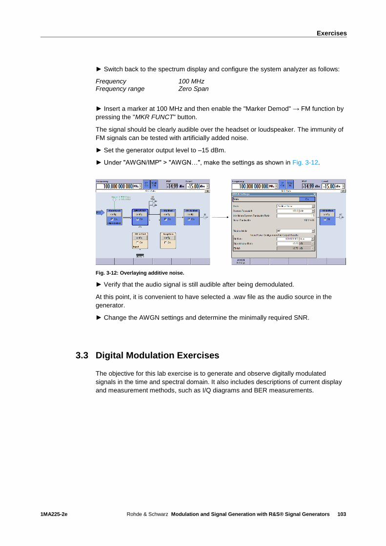
Exercises
1MA225-2e Rohde & Schwarz Modulation and Signal Generation with R&S® Signal Generators
103
Switch back to the spectrum display and configure the system analyzer as follows:
Frequency 100 MHz Frequency range Zero Span
Insert a marker at 100 MHz and then enable the "Marker Demod" → FM function by
pressing the "MKR FUNCT" button.
The signal should be clearly audible over the headset or loudspeaker. The immunity of
FM signals can be tested with artificially added noise.
Set the generator output level to –15 dBm.
Under "AWGN/IMP" > "AWGN…", make the settings as shown in Fig. 3-12.
Fig. 3-12: Overlaying additive noise.
Verify that the audio signal is still audible after being demodulated.
At this point, it is convenient to have selected a .wav file as the audio source in the
generator.
Change the AWGN settings and determine the minimally required SNR.
3.3 Digital Modulation Exercises
The objective for this lab exercise is to generate and observe digitally modulated
signals in the time and spectral domain. It also includes descriptions of current display
and measurement methods, such as I/Q diagrams and BER measurements.
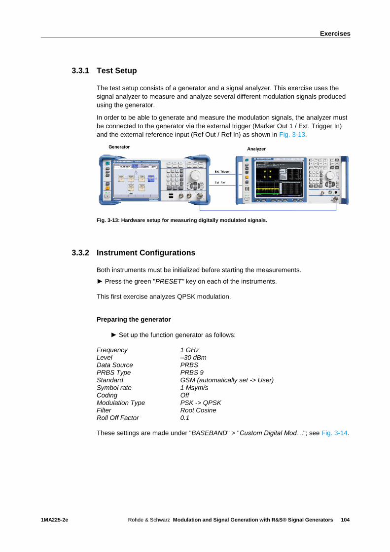
Exercises
1MA225-2e Rohde & Schwarz Modulation and Signal Generation with R&S® Signal Generators
104
3.3.1 Test Setup
The test setup consists of a generator and a signal analyzer. This exercise uses the
signal analyzer to measure and analyze several different modulation signals produced
using the generator.
In order to be able to generate and measure the modulation signals, the analyzer must
be connected to the generator via the external trigger (Marker Out 1 / Ext. Trigger In)
and the external reference input (Ref Out / Ref In) as shown in Fig. 3-13.
Fig. 3-13: Hardware setup for measuring digitally modulated signals.
3.3.2 Instrument Configurations
Both instruments must be initialized before starting the measurements.
Press the green "PRESET" key on each of the instruments. This first exercise analyzes QPSK modulation.
Preparing the generator
Set up the function generator as follows: Frequency 1 GHz Level –30 dBm Data Source PRBS PRBS Type PRBS 9 Standard GSM (automatically set -> User) Symbol rate 1 Msym/s Coding Off Modulation Type PSK -> QPSK Filter Root Cosine Roll Off Factor 0.1
These settings are made under "BASEBAND" > "Custom Digital Mod…"; see Fig. 3-14.
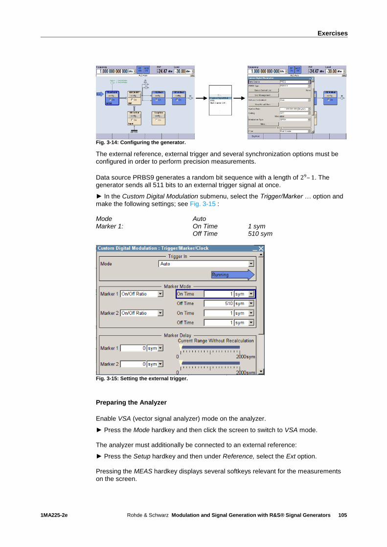
Exercises
1MA225-2e Rohde & Schwarz Modulation and Signal Generation with R&S® Signal Generators
105
Fig. 3-14: Configuring the generator.
The external reference, external trigger and several synchronization options must be configured in order to perform precision measurements.
Data source PRBS9 generates a random bit sequence with a length of 29– 1. The generator sends all 511 bits to an external trigger signal at once.
In the Custom Digital Modulation submenu, select the Trigger/Marker … option and make the following settings; see Fig. 3-15 : Mode Auto Marker 1: On Time 1 sym Off Time 510 sym
Fig. 3-15: Setting the external trigger.
Preparing the Analyzer
Enable VSA (vector signal analyzer) mode on the analyzer.
Press the Mode hardkey and then click the screen to switch to VSA mode. The analyzer must additionally be connected to an external reference:
Press the Setup hardkey and then under Reference, select the Ext option. Pressing the MEAS hardkey displays several softkeys relevant for the measurements on the screen.
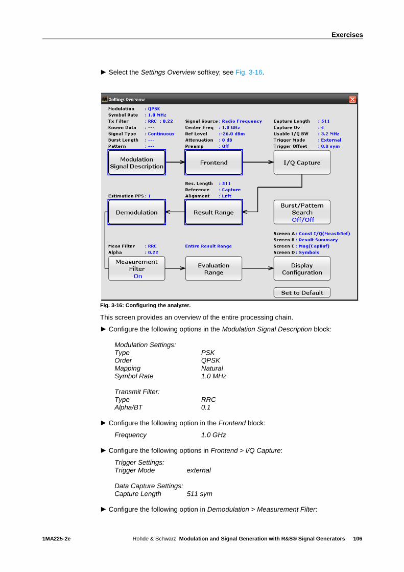
Exercises
1MA225-2e Rohde & Schwarz Modulation and Signal Generation with R&S® Signal Generators
106
Select the Settings Overview softkey; see Fig. 3-16.
Fig. 3-16: Configuring the analyzer.
This screen provides an overview of the entire processing chain.
Configure the following options in the Modulation Signal Description block: Modulation Settings: Type PSK Order QPSK Mapping Natural Symbol Rate 1.0 MHz Transmit Filter: Type RRC Alpha/BT 0.1 Configure the following option in the Frontend block:
Frequency 1.0 GHz Configure the following options in Frontend > I/Q Capture:
Trigger Settings: Trigger Mode external Data Capture Settings: Capture Length 511 sym Configure the following option in Demodulation > Measurement Filter:
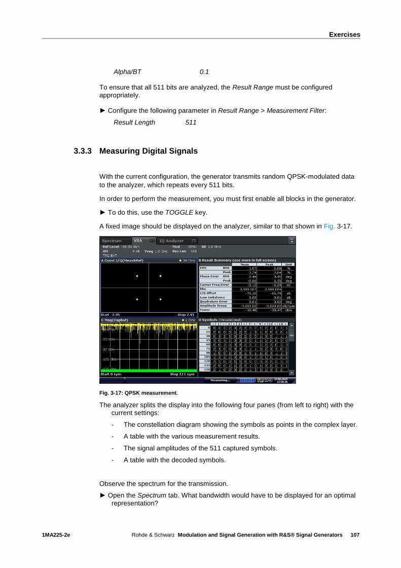
Exercises
1MA225-2e Rohde & Schwarz Modulation and Signal Generation with R&S® Signal Generators
107
Alpha/BT 0.1 To ensure that all 511 bits are analyzed, the Result Range must be configured appropriately. Configure the following parameter in Result Range > Measurement Filter:
Result Length 511
3.3.3 Measuring Digital Signals
With the current configuration, the generator transmits random QPSK-modulated data
to the analyzer, which repeats every 511 bits.
In order to perform the measurement, you must first enable all blocks in the generator.
To do this, use the TOGGLE key.
A fixed image should be displayed on the analyzer, similar to that shown in Fig. 3-17.
Fig. 3-17: QPSK measurement.
The analyzer splits the display into the following four panes (from left to right) with the current settings:
- The constellation diagram showing the symbols as points in the complex layer.
- A table with the various measurement results.
- The signal amplitudes of the 511 captured symbols.
- A table with the decoded symbols.
Observe the spectrum for the transmission.
Open the Spectrum tab. What bandwidth would have to be displayed for an optimal representation?

Exercises
1MA225-2e Rohde & Schwarz Modulation and Signal Generation with R&S® Signal Generators
108
On the generator, change the rolloff factor for the filter. How does this change affect
the spectrum, and what effects can be expected for the signal transmission? Transitions between the possible states are often of interest as well. The IQ Analyzer
displays all measured signal states.
Press the Mode hardkey and select IQ Analyzer.
Under Display Config, select the IQ Vector option and then use the Level function to
optimally adjust the results. Your display should look something like Fig. 3-18.
The effects of the rolloff factor are not limited to the spectrum; the influence of these
variables is also clearly visible in the I/Q vector display.
What changes would you expect at various rolloff factors?
Change the factor to various positions across the entire range and verify your
assumptions.
Fig. 3-18: I/Q diagram for QPSK.
Influence of I/Q impairments during QPSK modulation
The R&S® SMBV generator supports a wide variety of options for influencing the signal
quality.
What would be the result of switching on the quadrature offset?
On the generator, go to I/Q Mod > I/Q Settings. Set the options as follows:
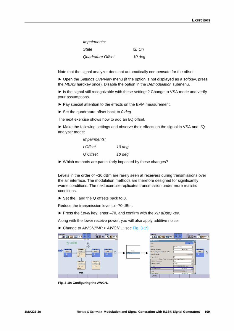
Exercises
1MA225-2e Rohde & Schwarz Modulation and Signal Generation with R&S® Signal Generators
109
Impairments:
State On
Quadrature Offset 10 deg
Note that the signal analyzer does not automatically compensate for the offset.
Open the Settings Overview menu (if the option is not displayed as a softkey, press
the MEAS hardkey once). Disable the option in the Demodulation submenu.
Is the signal still recognizable with these settings? Change to VSA mode and verify
your assumptions.
Pay special attention to the effects on the EVM measurement.
Set the quadrature offset back to 0 deg.
The next exercise shows how to add an I/Q offset.
Make the following settings and observe their effects on the signal in VSA and I/Q
analyzer mode:
Impairments:
I Offset 10 deg
Q Offset 10 deg
Which methods are particularly impacted by these changes? Levels in the order of –30 dBm are rarely seen at receivers during transmissions over
the air interface. The modulation methods are therefore designed for significantly
worse conditions. The next exercise replicates transmission under more realistic
conditions.
Set the I and the Q offsets back to 0.
Reduce the transmission level to –70 dBm.
Press the Level key, enter –70, and confirm with the x1/ dB(m) key.
Along with the lower receive power, you will also apply additive noise.
Change to AWGN/IMP > AWGN…; see Fig. 3-19.
Fig. 3-19: Configuring the AWGN.

Exercises
1MA225-2e Rohde & Schwarz Modulation and Signal Generation with R&S® Signal Generators
110
Set the options as follows: State On Carrier/Noise Ratio 15 dB Observe the effects on the constellation diagram and on the spectrum. How low does the SNR need to be for this transmission? Check the result against your assumptions. Can interference-free transmission still be expected for a signal as shown in Fig. 3-20. What exactly does the EVM measurement show, and where can this value be found?
Fig. 3-20: Low SNR with QPSK.
Frequently, an RRC filter is used during transmission to suppress intersymbol
interference (ISI). This filter is typically split into two parts in order to achieve the best
possible noise suppression: One filter is located in the transmitter and one in the
receiver, and the two combined provide a raised cosine transfer function.
Does changing the rolloff factor affect the EVM measurement? What factor provides
the best result readings, and why is this factor not used in practice?
Test other filters and their behavior with interference. Make note of the required
settings on the transmitter and the receiver end.
Switch back to the RRC filter.
Using QPSK modulation places special demands on the amplifier that are particularly
disadvantageous for mobile devices.
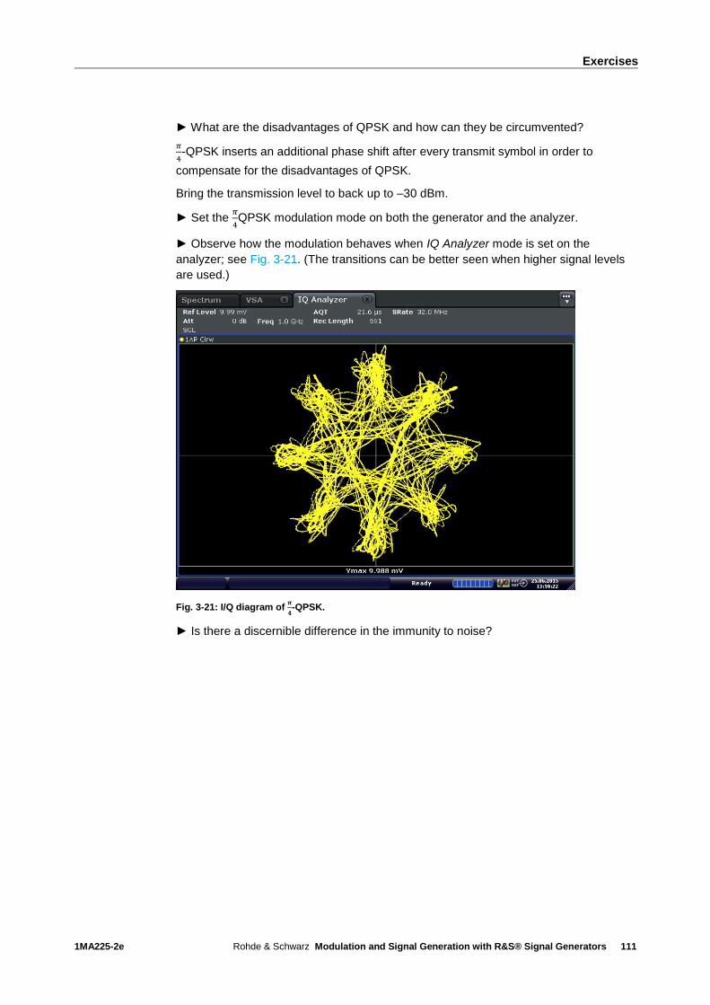
Exercises
1MA225-2e Rohde & Schwarz Modulation and Signal Generation with R&S® Signal Generators
111
What are the disadvantages of QPSK and how can they be circumvented?
𝜋
4-QPSK inserts an additional phase shift after every transmit symbol in order to
compensate for the disadvantages of QPSK.
Bring the transmission level to back up to –30 dBm.
Set the 𝜋
4QPSK modulation mode on both the generator and the analyzer.
Observe how the modulation behaves when IQ Analyzer mode is set on the
analyzer; see Fig. 3-21. (The transitions can be better seen when higher signal levels
are used.)
Fig. 3-21: I/Q diagram of 𝝅
𝟒-QPSK.
Is there a discernible difference in the immunity to noise?

Exercises
1MA225-2e Rohde & Schwarz Modulation and Signal Generation with R&S® Signal Generators
112
QAM signals
With QAM modulation, the available signal space is improved by adding signal states.
Set modulation mode 16-QAM on both the generator and the analyzer.
Add the same I and Q offsets as used above for QPSK. Evaluate the results; see
also Fig. 3-22.
Test a variety of SNR values and compare them against the result gained during the
QPSK measurements.
Fig. 3-22: 16-QAM with I and Q distortions.
This next exercise shows how to work with data lists, which can replace random
sequences. Data lists provide for better synchronization and unambiguous
demodulation, and can also be used for bit error rate measurements.
In this section, you will create a data list on the generator and demodulate the data
using the signal generator and an appropriate synchronization sequence.
In the Custom Digital Modulation screen, select submenu Data Source and then the
List Management option.
Press Select Data List to Edit > New List, then select a memory location and assign
a name for the new list.
Select the new list and fill it with 32 hexadecimal values; see Fig. 3-23.

Exercises
1MA225-2e Rohde & Schwarz Modulation and Signal Generation with R&S® Signal Generators
113
Fig. 3-23: Creating a data list with 32 hexadecimal values.
Because the bit sequence is known, there is no longer any need for an external trigger.
In submenu I/Q Capture, switch to trigger mode Free Run; see Fig. 3-16.
Set a Capture Length of 256 symbols.
By using a known pattern, it is possible to demodulate the QPSK-modulated signal
unambiguously. This requires that a segment of the data be supplied to the analyzer.
Press the MEAS CONFIG hardkey and select submenu Config Pattern.
Under All Patterns, select New to create a new pattern. Select a segment of the
previously created list and fill in the remaining fields as appropriate; see Fig. 3-24.
Fig. 3-24: Creating a known pattern.
Save the pattern and apply the settings to the Predefined Patterns column.
Use Burst/Pattern Search to load the saved pattern. The analyzer should detect the
bit sequence in the signal and synchronize it correctly; see Fig. 3-25.
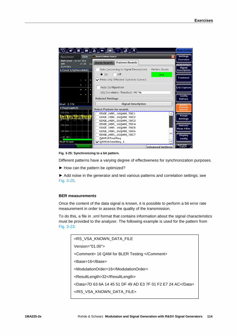
Exercises
1MA225-2e Rohde & Schwarz Modulation and Signal Generation with R&S® Signal Generators
114
Fig. 3-25: Synchronizing to a bit pattern.
Different patterns have a varying degree of effectiveness for synchronization purposes.
How can the pattern be optimized?
Add noise in the generator and test various patterns and correlation settings; see
Fig. 3-25.
BER measurements
Once the content of the data signal is known, it is possible to perform a bit error rate
measurement in order to assess the quality of the transmission.
To do this, a file in .xml format that contains information about the signal characteristics
must be provided to the analyzer. The following example is used for the pattern from
Fig. 3-23:
<RS_VSA_KNOWN_DATA_FILE
Version="01.00">
<Comment> 16 QAM for BLER Testing </Comment>
<Base>16</Base>
<ModulationOrder>16</ModulationOrder>
<ResultLength>32</ResultLength>
<Data>7D 63 6A 14 45 51 DF 49 AD E3 7F 01 F2 E7 24 AC</Data>
</RS_VSA_KNOWN_DATA_FILE>

Exercises
1MA225-2e Rohde & Schwarz Modulation and Signal Generation with R&S® Signal Generators
115
Load the file into the R&S® FSV.
In the Modulation Signal Description menu, use the Known Data option to load the
data.
Complete the remaining settings as shown in Fig. 3-26.
The QAM16TestSeq pattern includes the full contents for the transmission (7Dh …
ACh).
Configure the BER measurement under Display Configuration > Modulation
Accuracy > Bit Error Rate.
Fig. 3-26: Configuring the BER measurement.
At low noise, the results will be as shown in Fig. 3-27.

Exercises
1MA225-2e Rohde & Schwarz Modulation and Signal Generation with R&S® Signal Generators
116
Fig. 3-27: BER measurement under good conditions.
UMTS signals
In this last set of exercises, a simple UMTS cellular signal will be generated and
several parameters measured. The objective is to gain an understanding of the
spectrum and the basic structure of WCDMA signals.
Configure the signal generator for UMTS signals:
In the Baseband block, open 3GPP FDD (found under CDMA Standards).
Use State > On to enable the generation of UMTS signals.
Increase the frequency to 2110 MHz (band 1).
The generator produces downlink UMTS signals from a simulated base station.
Ensure that the analyzer is set to the correct frequency and observe the spectrum of
the WCDMA transmission.
The analyzer must be in 3G FDD BTS mode in order to measure a UMTS base station.
Press the MODE hardkey to change to 3G FDD BTS mode.
Before starting a measurement, you should familiarize yourself with the possible
analyzer settings in this mode.
Use the Settings Overview softkey to open the summary display; see Fig. 3-28.
The first measurement (Fig. 3-29) displayed when you change to 3G FDD BTS mode
shows the level for all detected channels (yellow) in the selected slot. Codes that
cannot be allocated to a channel are shown in turquoise.

Exercises
1MA225-2e Rohde & Schwarz Modulation and Signal Generation with R&S® Signal Generators
117
What is the purpose of the Channelization Codes and the Scrambling Codes?
Fig. 3-28: Overview of UMTS settings.
Fig. 3-29: Display of all detected channels and their level.
The R&S®FSV also allows simultaneous measurement of the levels of adjacent
channels (ACLR), the allocated bandwidth and spectrum masks (SEM).
Start the RF Combi measurement.
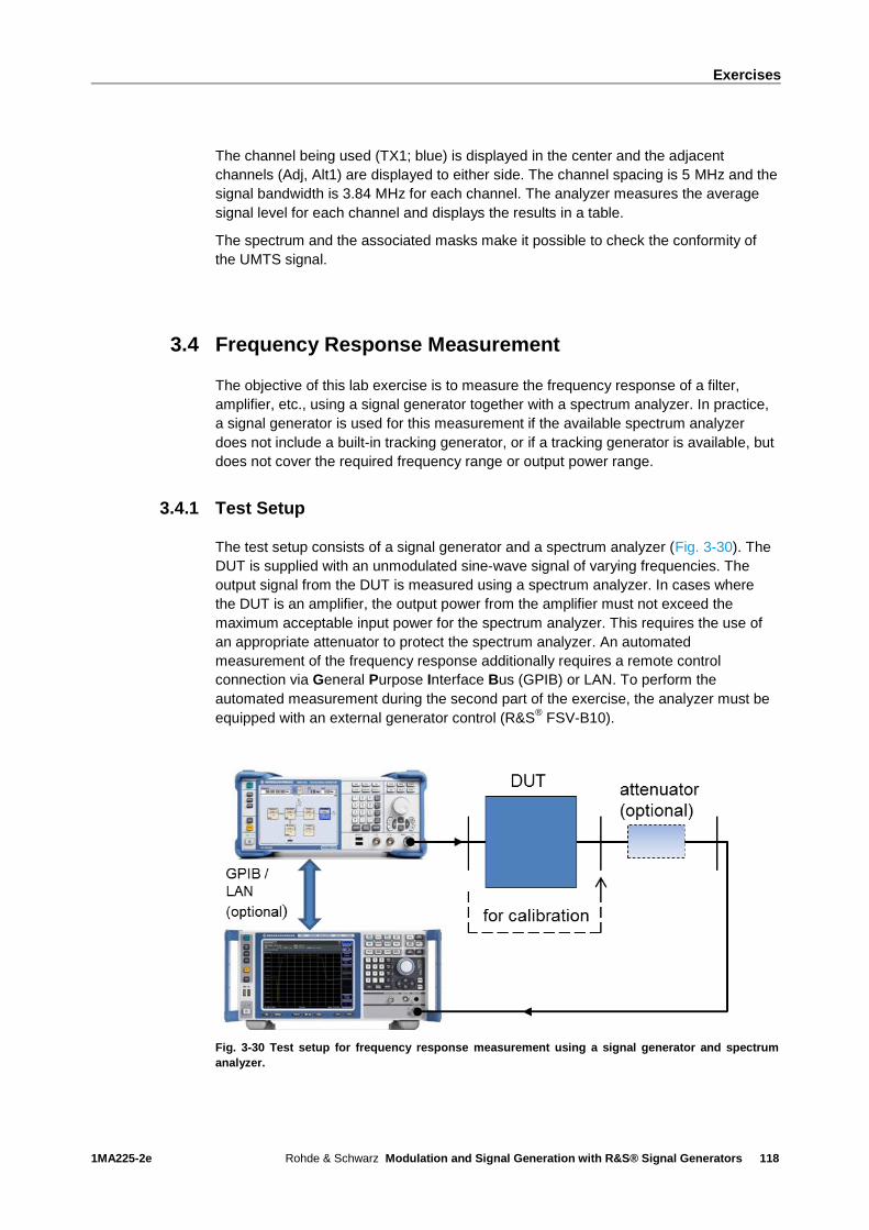
Exercises
1MA225-2e Rohde & Schwarz Modulation and Signal Generation with R&S® Signal Generators
118
The channel being used (TX1; blue) is displayed in the center and the adjacent
channels (Adj, Alt1) are displayed to either side. The channel spacing is 5 MHz and the
signal bandwidth is 3.84 MHz for each channel. The analyzer measures the average
signal level for each channel and displays the results in a table.
The spectrum and the associated masks make it possible to check the conformity of
the UMTS signal.
3.4 Frequency Response Measurement
The objective of this lab exercise is to measure the frequency response of a filter,
amplifier, etc., using a signal generator together with a spectrum analyzer. In practice,
a signal generator is used for this measurement if the available spectrum analyzer
does not include a built-in tracking generator, or if a tracking generator is available, but
does not cover the required frequency range or output power range.
3.4.1 Test Setup
The test setup consists of a signal generator and a spectrum analyzer (Fig. 3-30). The
DUT is supplied with an unmodulated sine-wave signal of varying frequencies. The
output signal from the DUT is measured using a spectrum analyzer. In cases where
the DUT is an amplifier, the output power from the amplifier must not exceed the
maximum acceptable input power for the spectrum analyzer. This requires the use of
an appropriate attenuator to protect the spectrum analyzer. An automated
measurement of the frequency response additionally requires a remote control
connection via General Purpose Interface Bus (GPIB) or LAN. To perform the
automated measurement during the second part of the exercise, the analyzer must be
equipped with an external generator control (R&S® FSV-B10).
Fig. 3-30 Test setup for frequency response measurement using a signal generator and spectrum
analyzer.
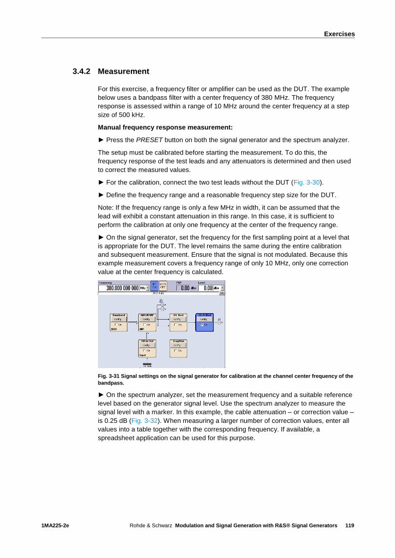
Exercises
1MA225-2e Rohde & Schwarz Modulation and Signal Generation with R&S® Signal Generators
119
3.4.2 Measurement
For this exercise, a frequency filter or amplifier can be used as the DUT. The example
below uses a bandpass filter with a center frequency of 380 MHz. The frequency
response is assessed within a range of 10 MHz around the center frequency at a step
size of 500 kHz.
Manual frequency response measurement:
Press the PRESET button on both the signal generator and the spectrum analyzer.
The setup must be calibrated before starting the measurement. To do this, the
frequency response of the test leads and any attenuators is determined and then used
to correct the measured values.
For the calibration, connect the two test leads without the DUT (Fig. 3-30).
Define the frequency range and a reasonable frequency step size for the DUT.
Note: If the frequency range is only a few MHz in width, it can be assumed that the
lead will exhibit a constant attenuation in this range. In this case, it is sufficient to
perform the calibration at only one frequency at the center of the frequency range.
On the signal generator, set the frequency for the first sampling point at a level that
is appropriate for the DUT. The level remains the same during the entire calibration
and subsequent measurement. Ensure that the signal is not modulated. Because this
example measurement covers a frequency range of only 10 MHz, only one correction
value at the center frequency is calculated.
Fig. 3-31 Signal settings on the signal generator for calibration at the channel center frequency of the
bandpass.
On the spectrum analyzer, set the measurement frequency and a suitable reference
level based on the generator signal level. Use the spectrum analyzer to measure the
signal level with a marker. In this example, the cable attenuation – or correction value –
is 0.25 dB (Fig. 3-32). When measuring a larger number of correction values, enter all
values into a table together with the corresponding frequency. If available, a
spreadsheet application can be used for this purpose.

Exercises
1MA225-2e Rohde & Schwarz Modulation and Signal Generation with R&S® Signal Generators
120
Fig. 3-32 Measuring the correction value at the bandpass center frequency.
As shown in Fig. 3-30, connect the DUT between the signal generator and the
spectrum analyzer.
On the signal generator, set all of the measurement frequencies with the defined
step size, then use the spectrum analyzer to measure the output level at the DUT.
Enter the measured values for each of the calibration values into a column of the table
next to the corresponding correction values.
Fig. 3-33 shows the example measurement result. A spreadsheet application can
easily display the measured values of the frequency response graphically.
Fig. 3-33 Frequency response of a bandpass.
Automated frequency response measurement:
An external generator control greatly simplifies the frequency response measurement.
This control, which is typically available as an option, allows the spectrum analyzer to
control the generator frequency synchronously with its frequency sweep.
Connect the signal generator to the GPIB port on the R&S® FSV-B10 option or via
LAN.
Settings on the R&S® FSV:
Set the frequency range and reference level required for the measurement.
Press the INPUT/OUTPUT button and then select Tracking Generator -> Source
Config.

Exercises
1MA225-2e Rohde & Schwarz Modulation and Signal Generation with R&S® Signal Generators
121
Configure the generator level and set Source Freq. Coupling to Auto. Auto sets the
frequency range to match that on the spectrum analyzer.
Configure the interface (generator type, LAN or GPIB and device address).
Fig. 3-34 External tracking generator settings.
Switch on the generator by setting the source to RF EXTERNAL 1 ON.
Calibration:
Connect the two test leads (without the DUT).
Select Source Cal.
Start the calibration with Calibrate Transmission and wait until the calibration
completes.
As shown in Fig. 3-30, connect the DUT between the signal generator and the
spectrum analyzer.
The spectrum analyzer display will show the frequency response of the DUT as shown
in Fig. 3-35.
Fig. 3-35 Automated frequency response measurement using an external signal generator as the
tracking generator.

Exercises
1MA225-2e Rohde & Schwarz Modulation and Signal Generation with R&S® Signal Generators
122
What advantages does an automated measurement provide over a manual
measurement?
Consider the results in Fig. 3-33 and Fig. 3-35. How can the differing curve
characteristics be explained?
What influences can be corrected with the calibration?

Literature
1MA225-2e Rohde & Schwarz Modulation and Signal Generation with R&S® Signal Generators
123
4 Literature
[1] Analog Devices. 1999. A Technical Tutorial on Digital Signal Synthesis. 1999.
[2] Dr. Banerjee, Markus. 2001. Möglichkeiten und Genauigkeiten der
elektronischen Pegeleinstellung. 2001. NEUES von Rohde & Schwarz® Heft 171.
[3] Liebl, Detlev. 2014. Moderne Mobilfunkmessungen. Educational Note. s.l. :
Rohde & Schwarz®, 2014. 1MA231_3d.
[4] Mäusl, Rudolf. 1988. Analoge Modulationsverfahren. s.l. : Hüthig Verlag, 1988.
Vol. 1.
[5] —. 1991. Digitale Modulationsverfahren. s.l. : Hüthig Verlag, 1991. Vol. 2.
[6] National Instruments. 2015. NI Tutorial. Understanding Direct Digital Synthesis.
2015.
[7] Pehl, Erich. 1998. Digitale und analoge Nachrichtenübertragung. s.l. : Hüthig
Verlag, 1998. 2.
[8] R&S® SMB100A RF and Microwave Signal Generator Brochure.
[9] R&S® SMBV100A Vector Signal Generator User Manual.
[10] R&S® SMF Microwave Signal Generator Brochure.
[11] R&SV® SMBV100A Vector Signal Generator SMBV100A Specifications Data
Sheet 6.00.
[12] Rauscher, Christoph. 2011. Grundlagen der Spektrumanalyse. s.l. : Rohde &
Schwarz®, 2011. 5.
[13] Rohde & Schwarz®. Digitale Modulation im Mobilfunk. PD 757.3470.12.
[14] —. Spannungs- und Leistungsmeßtechnik. PD 757.0835.13.
[15] Texas Instruments. 1999. Fractional/Integer-N PLL Basics. 1999. Technical Brief
SWRA029.
[16] Wolf, Josef. 1995. Messung des Phasenrauschens mit den
Spektrumanalysatoren der FSE-Familie. Application Note 1EPAN 16D. s.l. :
Rohde & Schwarz, 1995.

Rohde & Schwarz
The Rohde & Schwarz electronics group offers
innovative solutions in the following business fields:
test and measurement, broadcast and media, secure
communications, cybersecurity, radiomonitoring and
radiolocation. Founded more than 80 years ago, this
independent company has an extensive sales and
service network and is present in more than 70
countries.
The electronics group is among the world market
leaders in its established business fields. The
company is headquartered in Munich, Germany.
Regional headquarters are located in Singapore and
in Columbia, Maryland in the U.S.
Regional contact
Europe, Africa, Middle East +49 89 4129 12345 [email protected] North America 1 888 TEST RSA (1 888 837 87 72) [email protected] Latin America +1 410 910 79 88 [email protected] Asia Pacific +65 65 13 04 88 [email protected]
China +86 800 810 82 28 |+86 400 650 58 96 [email protected]
Sustainable product design
ı Environmental compatibility and eco-footprint
ı Energy efficiency and low emissions
ı Longevity and optimized total cost of ownership
This document and any included programs may be
used only upon acceptance of the terms and
conditions of use as defined in the downloads area
of the Rohde & Schwarz Internet site.
R&S ® is a registered trademark of Rohde & Schwarz GmbH &
Co. KG Trade names are trademarks of the owners