module -18 flip flops 1. 2. 3. the trigger signal 4
TRANSCRIPT
1
Electronic Science Digital Electronics
18. Flip flops
Module -18 Flip flops
1. Introduction
2. Comparison of latches and flip flops.
3. Clock – the trigger signal
4. Flip flops
4.1. Level triggered flip flops – SR, D and JK flip flops
4.2. Edge triggered flip flops
4.3. Master slave flip flops
4.4. Flip flop ICs
4.5. Operating characteristics
5. Applications of flip flops
6. Summary
Learning objectives
1. To understand the difference between latches and flip flops.
2. To study the principles of triggering methods
3. To learn about construction and working of RS, D, JK and T flip flops
4. To know the applications of flip flops

2
Electronic Science Digital Electronics
18. Flip flops
1. Introduction
Latches and flip flops are memory devices used in the construction of Sequential circuits. These memory devices can remain in the same state even if the inputs are removed. These devices can hold a binary value 0 or 1 until is forced to change state. Latches and flip flops are bistable devices. But they differ in the way the change their state. Latches are asynchronous bistable devices where latch accepts the input signal as soon as it changes and does not require any external timing signal. A flip flop is a memory device which accepts the input only in synchronism with the timing signal known as the clock. The clock may be in the form of level, or an edge or a pulse. A level trigger means that the flip flop accepts the input depending upon voltage -high level or low level. An edge trigger changes the flip flop condition at rising edge (positive edge) or falling (negative) edge. The low to high transition on the clock is a rising edge or positive going edge and high to low transition is known as falling edge or negative going edge. In addition, there is pulse trigger signal on the clock to change the state. There are four types of flip flops used for storing 1-bit information namely SR, D, JK and T flip flop. Flip-flops are digital logic circuits that can be in one of two states. Flip-flops maintain their state indefinitely until an input pulse called a trigger is received. When a trigger is received, the flip-flop outputs change state according to defined rules and remain in those states until another trigger is received.
2. Comparison between latches and Flip flops
Latches and flip flops are sequential circuits capable of storing an information and find applications in many electronic gadgets. Figure-1 indicates the comparison table for latches and flip flops. First column in the table includes important keywords or parameters used for the comparison.
Latches are asynchronous bistable multivibrator devices whereas flip flops are synchronous bistable multivibrator devices. Latches and flip flops are the basic elements and these are used to store information. One flip flop and latch can store one bit of data, hence referred to as 1-bit memory cell. Latch can hold the data without gating or clocking signal. Certain latches can use enable signal for gating the data into the latch. It changes state whenever the enable is asserted. Flip flops can store the data in synchronism with a clock signal. Flip flops can be clocked as level, edge or pulse triggering methods.

3
Electronic Science Digital Electronics
18. Flip flops
Latches Flip flops
Principle Asynchronous bistable Synchronous bistable
Storage 1-bit memory cell 1-bit memory cell
Gating or
clocking
mechanism
Either absent or use of enable signal Level , edge or pulse trigger
State change Checks the input continuously and
changes the output as soon as the input changes (after a small propagation
delay).
Checks the input continuously and
changes the output only at time determined by clock
Sensitivity Similar to Level sensitive FF Edge or pulse sensitive FF
Figure-1: Comparison table of Latches and Flip flops.
The main difference between the latches and flip flops is the way how state changes. A latch checks input continuously and changes the output whenever there is a change in input. But, flip flop is a combination of latch and a clock which continuously checks input and changes the output only at time determined by the clock. Latches can be treated just similar to a level triggered flip flop, where the voltage level decides the enabling of the flip flop. Flip flops can be either edge or pulse sensitive.
2. Clock- the trigger signal
Figure 2: Clock – the trigger signal
A clock is a periodic signal that changes between 0 and 1 or low level and high level. The time it takes for a waveform to repeat is called a period (T). The frequency of a clock is the inverse of the period. Thus, f = 1/T. The smaller the period, the larger the frequency. Frequency is measured as s-1 which is inverse seconds. This is also called Hertz, abbreviated Hz. Usually a clock provides output 1 half the time and output 0for the other half, such signal is referred to as a square wave. Clock signal can have unequal time for high and low states,
4
Electronic Science Digital Electronics
18. Flip flops
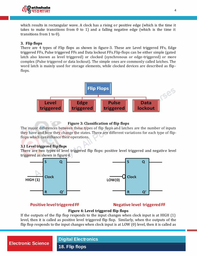
which results in rectangular wave. A clock has a rising or positive edge (which is the time it takes to make transitions from 0 to 1) and a falling negative edge (which is the time it transitions from 1 to 0). 3. Flip flops There are 4 types of Flip flops as shown in figure-3. These are Level triggered FFs, Edge triggered FFs, Pulse triggered FFs and Data lockout FFs.Flip-flops can be either simple (gated latch also known as level triggered) or clocked (synchronous or edge-triggered) or more complex (Pulse triggered or data lockout). The simple ones are commonly called latches. The word latch is mainly used for storage elements, while clocked devices are described as flip -flops.
Figure 3: Classification of flip flops
The major differences between these types of flip flops and latches are the number of inputs they have and how they change the states. There are different variations for each type of flip-flops which can enhance their operations.
3.1 Level triggered flip flops
There are two types of level triggered flip flops: positive level triggered and negative level triggered as shown in figure 4.
Figure 4: Level triggered flip flops
If the outputs of the flip flop responds to the input changes when clock input is at HIGH (1) level, then it is called as positive level triggered flip flop. Similarly, when the outputs of the flip flop responds to the input changes when clock input is at LOW (0) level, then it is called as

5
Electronic Science Digital Electronics
18. Flip flops
negative level triggered flip flop. Negative level triggered flip flop has bubble at clock input indicating negative level triggered input. Level triggering is not used practically because of similarity with the latches. Latches are basically are level sensitive. The difference between a gated latch and level triggered flip flop is that latch has enable input and level triggered flip flop has clock input. Level clocking means FF responds either on LOW level of clock or HIGH level of clock. HIGH level clock is termed as positive level triggered and LOW level clocked is also termed as negative level clock. Positive level triggered SR flip flop The logic symbol of SR flip contains two SR inputs, a clock input and complementary outputs Q and Q’ is shown in figure 5. The logic diagram contains two sections: gating circuit for latch with clock input and an active low cross coupled NAND latch. When clock input is at High level (1), S and R inputs controls the state of latch.
Figure 5: Positive level triggered SR flip flop.
When Clock is 1 and both S and R inputs are 0 then inputs to latch are 11. Therefore, Q and Q’ will not change. The output remains in the last state. The output of SR flip flop will be RESET, if clock input is High and SR inputs are 01. The SR flip flop output goes High when clock input is 1 and SR inputs are 10. This is a SET condition for the flip flop. If both SR inputs are high (1) then the flip flop generates invalid output i.e. both Q and Q’ are at 0 level. This generates invalid condition, which is not allowed. When clock level is 0 then irrespective of S and R inputs latch inputs at high (1) state. Therefore, both the outputs do not change. Thus last state is maintained. Negative level triggered SR flip flop The logic symbol, logic diagram and truth table for negative level triggered SR flip flop are shown in figure 6. The Clock input has the bubble at the input in the logic symbol and inverter is inserted at the clock input in the logic diagram.

6
Electronic Science Digital Electronics
18. Flip flops
Figure 6: Negative level triggered SR flip flop.
The truth table of SR flip flop is generated at the negative level (0) applied to the clock input. The S and R inputs decide the state of the flip flop i.e. SET, RESET, No Change or Invalid.
Positive level triggered D flip flop
The gated D flip flop has only one input along with the clock input. This input is a D or data input. The logic symbol and logic diagram indicates that it is a positive level triggered flip flop as shown in figure 7.
Figure 7: Positive level triggered D flip flop.
When the clock input is high, the Q output follows the input D. It is possible to store data 0 or 1 in the flip flop. When D=0 then flip flop output is RESET state and at D=1, the flip flops stores 1 i.e. SET state. During low level of clock irrespective of the value of D input, the Q output of flip flop do not change irrespective of D input. Thus flip flop keeps the last state. As the inputs appear at output after some delay, hence D flip flop is also called as Delay flip flop.

7
Electronic Science Digital Electronics
18. Flip flops
Positive level triggered JK flip flop The basic SR flip circuit has many applications but it has some switching problems. First, when both S and R input are at logic 1 then SR flip flop generate invalid or not allowed condition, which must always be avoided. Similarly, if S or R input changes when clock is active then the correct latching action may not occur. To overcome these two problems with SR flip flop, the JK flip flop is developed. The JK flip flop is considered to be a universal flip flop because it is possible to convert JK flip flop into any other types of flip flops like SR or D type. The logic symbol of this flip flop includes JK inputs along with Clock input. The JK flip flop is exactly the same as the SR flip flop except the difference is that it does not generate invalid or not allowed condition. The logic diagram of flip flop indicates that both S and R inputs of SR flip flop are replaced by two inputs called the J and K inputs respectively i.e. J=S and K=R. The name JK flip flop is given after its inventor Jack Kilby. Second modification in the logic diagram is that the two input NAND gates of gated SR flip flop are now replaced by two 3-input NAND gates. The third input of NAND gates are connected cross-coupled fashion i.e. Q output is connected to K side and Q’ is connected to the J side of flip flop as shown in figure 8. This cross coupling removes the invalid condition when S=1 and R=1 and replaces it by a toggle output condition.
Figure 8: Positive level triggered JK flip flop
Let us now talk about the truth table of JK flip flop. The JK flip flop is basically an SR flip flop with feedback which enables only one of its two inputs to be active at any given time. When clock is High (i.e. logic 1) and both JK inputs are 00 then, the latch output do not change. Thus JK flip flop holds the last state. The flip flop enters into RESET mode (i.e. Q=0), when J=0 and K=1 with high state on clock. When J=1 and K=0, with clock input at High state, the output enter in SET mode by setting Q as 1. When clock as well as both J and K inputs are HIGH then output toggles from its previous state i.e. if Q=0 then it becomes 1 and if Q=1 then it becomes0. Let us consider Q=0 and Q’=1 then output of J side NAND gate provide 0 which changes the output to 1. Let us find out the change at k-side NAND gate. Q is initially 0, the K side NAND will provide output as 1 and with new Q as 1 the final Q’ changes to 0 from 1. Now let us consider a case when clock is inactive

8
Electronic Science Digital Electronics
18. Flip flops
i.e. when clock is Low (0), the outputs do not change irrespective of the JK inputs. This is once again the hold state of JK flip flop. Race-around condition The unpredictable or invalid condition of SR flip flop when both inputs are 1(S=R=1) is eliminated in a JK flip flop by using the feedback connection from outputs to the inputs. Therefore, changes in the output results change in input. Consider for example that the inputs J=K=1 and CLK=1. Let us assume Q=0. After a time t equal to propagation delay through two NAND gates in series the output will change to Q=1. Now we have J=K=1 and Q=1 and after another time t the output will change back to Q=0. Hence , we conclude that as long as CLK=1, the outputs will oscillate back and forth between 0 and 1. At the end of clock the output Q value is uncertain. This situation is referred to as the race around condition. To avoid racing, it is now important to think about different approach in designing the flip flop.
3.2 Edge triggered flip flops
Figure 9: Edge triggering
The problem of race around condition in the level triggered flip flop can be solved by ‘edge triggering’ the flip flop. Flip flops change state either at the positive edge (rising edge) or at the negative edge (falling) edge of the clock pulse as shown in figure 9.. These are also called as Low-to-high or High-to-low clock transitions. Positive edge triggered flip flops
Figure 10: Positive edge triggered flip flops
Positive edge triggered flip flops are those in which state transitions take place only at positive going (0 to 1) edge of the clock signal. Positive edge triggering is indicated by a triangle at the clock terminal of the flip flop as shown in figure 10. The positive edge triggered SR, D and JK flip flops are shown here.

9
Electronic Science Digital Electronics
18. Flip flops
Negative edge triggered flip flops
Figure 11: Negative edge triggered flip flops
Negative edge triggered flip flops are those in which state transitions take place only at negative going (1 to 0) edge of the clock signal. Negative edge triggering is indicated by a triangle along with small circle or bubble at the clock terminal of the flip flop. The negative edge triggered SR, D and JK flip flops are shown figure 11. Methods of edge triggering There are two methods of generating edge triggering for the flip flops. First simple method is by using RC differentiator circuit in the clock input of the flip flop. The second method is by using edge detector circuit. One way to make flip flop respond to a pulse transition positive or negative edges is to use capacitive coupling ( a differentiator circuit) as shown in figure 12. By designing, the RC time constant is much smaller than the clock’s pulse width. Because of this, the capacitor can charge fully when clock goes high. This exponential charging produces a narrow positive spike across the resistor. Later the negative edge of the pulse results in a narrow negative spike. The narrow positive spike enables FF for small duration and negative spike doe s nothing.
Figure 12: RC differentiator circuit for edge triggering
Many application do not use RC circuits to obtain narrow spikes because capacitors are difficult fabricate on chip for bipolar logic families like TTL. The most popular method for obtaining the narrow spikes is with the help of logic gate delay circuit.

10
Electronic Science Digital Electronics
18. Flip flops
Figure 13: Edge generator circuit for triggering
Let us consider a circuit to generate narrow pulse at positive edge of the clock. The inverter produces delay of a few nanoseconds. The AND gate produces an output spike that is HIGH only for few nanoseconds when CLK and CLK’ are both HIGH. This results in a narrow pulse at the output of the AND gate which occurs at positive going transition of the clock signal. Similarly a narrow positive spike is generated at the following edge of the clock by using an inverter and an active HIGH NOR gate (or active low AND) gate. The inverter produces a delay of few nanoseconds. The NOR gate produces an output spike that is HIGH only for few nanoseconds when both CLK and CLK’ are LOW. This results in a narrow pulse at the output of NOR gate which occurs at negative going transition of the clock. There are four edge triggered flip flops: SR, D, JK and T flip flops. Positive edge triggered SR flip flop
Inputs Outputs Mode
CLK S R Qn+1
0 0 Qn Last state (hold)
0 1 0 Reset
1 0 1 Set
1 1 ? Invalid
x x Qn Last state (hold)
Figure 14: Edge triggered SR flip flop

11
Electronic Science Digital Electronics
18. Flip flops
The logic symbol for edge triggered SR flip flop is shown in figure 14. The clock input is marked by the small angle indicates positive edge triggered flip flop and small circle or bubble before the angle mark indicates negative edge triggered flip flop. The positive edge triggered SR flip flop is activated at the positive going edge of the clock pulse. The implementation of SR flip flop shows an edge detector circuit, a gating circuit and basic latch. The SR inputs at the clock transition controls the output of SR flip flop. The flip flop respond at a LOW to HIGH transition of clock. The SR flip flop enters into SET or RESET mode depending on SR input condition and positive triggering transition of clock. Flip flop holds the last state when both S and R inputs are 0. Similarly, flip flop generates invalid output condition when both S and R inputs are at 1 logic at clock triggering transition. The outputs of FF will not change at either levels (HIGH or LOW) or the negative edge at the clock input. The input value at S and R inputs do not affect the output in such situation. Positive edge triggered D flip flop Let us now convert edge triggered SR flip flop into D flip flop. This edge triggered flip flop has only one input terminal called D input, in addition to the clock input. It is obtained by adding one inverter between S and R inputs as shown in figure 15. The logic symbols for edge triggered D flip flops is also shown here. The clock input is marked by the small triangle indicates positive edge triggered flip flop and small circle before the angle mark indicates negative edge triggered flip flop.
Figure 15a: Positive edge triggered D flip flop
Figure 15b: Truth table of edge triggered D flip flop
The Q output of D flip flop will have 0 state or 1 state depending on the value at D input either 0 or 1 respectively at positive or LOW to HIGH clock transition. In other words, output Q follows D input. The outputs of FF will not change at either levels at the negative edge or

12
Electronic Science Digital Electronics
18. Flip flops
(HIGH or LOW) at the clock input. The input value at D input do not affect the output in such situation. Thus the flip flop holds the last state during these triggering transitions. It can be noted that the negative edge triggered flip flop operates in the same way as positive edge triggered flip flop. Positive edge triggered JK flip flop
Figure 16: Positive edge triggered JK flip flop
The problem of race around condition associated with level triggered flip flop can be overcome by using edge triggered JK flip flop. When J=0 and K=0 at clock triggering transition, there is no change at the output of the flip flop. In short, the flip flop holds the last state as shown in figure 16. When J=0 and K=1 at Low to High transition, the flip flop enters in Reset state i.e. Q=0. Flip flop enters into SET state, when J=1 and K=0 at the positive clock transition. When J=1 and K=1 at positive triggering transition, the flip flop toggles i.e. goes to the complement of the present state. Note that, in this edge triggering method, the flip flop changes the state only once at the positive edge. Thus the problem of racing is avoided. The JK flip flop holds the last state at the negative edge or at either levels (HIGH or LOW) at the clock input. There is no change at the output of the JK flip flop. Positive edge triggered T flip flop
Figure 17: Positive edge triggered T flip flop

13
Electronic Science Digital Electronics
18. Flip flops
A T-flip flop has a single control input labeled as T for Toggle in addition to the positive clock triggering input as shown in figure 17. A JK flip flop can be converted into T flip flop just by connecting J and K inputs together. When T=0, the J and K input are at logic 0, the outputs do not change. Thus flip flop holds the last state. When T=1, both J and K inputs are at logic 1 and the flip flop toggles. i.e. goes to the complement of the present state. Note that, in the edge triggering method, the flip flop changes the state only once i.e. at the positive edge. Thus the problem of racing is avoided. All these changes are synchronized at the positive edge of the clock input. The T flip flop holds the last state at either levels (HIGH or LOW) or the negative edge at the clock input. Flip flop asynchronous inputs
Figure 18: Asynchronous inputs
Two extra inputs are often found on flip flops, either clear or preset the output. These inputs are effective at any time, thus are called asynchronous. If the Clear is at logic 0 then the output is forced to 0, irrespective of the other normal inputs as shown in figure 18. If the Preset is at logic 0 then the output is forced to 1, irrespective of the other normal inputs. The preset and the clear inputs cannot be 0 simultaneously. In the Preset and Clear are both 1 then the flip flop behaves according to its normal truth table. Pulse triggered flip flop A master slave flip flop is also called a pulse triggered flip flop because the length s of the time required for its output to change state equals the width of one clock pulse. In pulse triggered flip flops, data are entered into the flip flop on the leading edge of the clock pulse, but the output does not reflect input state until the fall ing edge of the clock pulse. The symbols of pulse triggered flip flops are shown in figure 19.
Figure 19: Pulse triggered flip flop

14
Electronic Science Digital Electronics
18. Flip flops
The inputs must be set prior to the clock rising edge of the clock pulse, but the output is postponed until the falling edge of the clock. Another restriction is the date inputs must not change while clock pulse is HIGH. The pulse triggered or master slave flip flop actually contains two flip flops – a master flip flop and a slave flip flop. Master Slave JK flip flop There are basically two sections – master section and slave section. The external control inputs (i.e. J, K and Clock) are applied to master JK section. The slave section is the same as the master section except that it is clocked on inverted clock pulse and is controlled by the outputs of the master section. The feedbacks from slave Q and Q’ are connected to master JK inputs. The master section assumes the state determined by the J and K inputs at the positive going edge of the clock pulse and the slave section at the negative going edge of the clock pulse. The state of the slave then immediately appears at Q and Q’ outputs. Q output of slave is connected back to NAND gate which receives K input of master and Q’ output is connected back into NAND ga te which receives J input of master.
Figure 20: Master Slave JK flip flop
When J=0 and K=0 at pulse triggering, there is no change at the output of the flip flop. In short, the flip flop holds the last state. When J=0 and K=1 at pulse trigger, the flip flop enters in Reset

15
Electronic Science Digital Electronics
18. Flip flops
state i.e. Q=0. Flip flop enters into SET state, when J=1 and K=0 at pulse clock transition. When J=1 and K=1 at triggering transition, the flip flop toggles i.e. goes to the complement of the present state. Note that, in this pulse triggering method, the flip flop changes the state only once after a clock pulse. Thus the problem of racing is avoided. Data lock out flip flops The major disadvantage of Master-slave flip flop is that the data inputs must be held constant while the clock is HIGH, because it responds to any changes in the data input. The data lock-out flip-flop is similar to the pulse-triggered (master-slave) flip-flop except it has a dynamic clock input i.e. edge triggering. This makes the flip flop sensitive to data inputs only during clock transitions. After the rising positive edge, the data inputs are disabled or locked out. Therefore, it is not necessary to hold data input constant while the clock pulse is HIGH. In short, master section of this flip-flop is like an edge-triggered device and the slave section becomes a pulse-triggered device to produce a postponed output on the falling edge of the clock pulse.
Figure 21: Symbols for data lock out flip flops
The logic symbols of S-R, J-K and D data lock-out flip-flops are shown in figure 21 with the dynamic input indicator as well as the postponed output symbol. Flip flop ICs
Positive edge triggered Flip flops
7470 JK flip flop with Preset and Clear
7474 Dual D flip flop with Preset and Clear
74174 Hex D flip flop with clear
74273 Octal D flip flop with Clear
74376 Quad JK flip flop with clear
Negative edge triggered Flip flops
74101 AND-OR gated JK flip flop with preset
74102 AND-OR gated JK flip flop with preset & Clear
74103 Dual JK with clear
74276 Quad JK with preset and clear

16
Electronic Science Digital Electronics
18. Flip flops
Level triggered Flip flops
7475 Dual 2 bit transparent latches
74100 Dual 4 bit transparent latches
74259 8-bit addressable latches with clear
Master Slave Flip flop
7473 Dual JK flip flop with clear
7474 Dual JK flip flop with preset and clear
Flip flop operating Characteristics
The operating characteristics and technical specifications of all the commercially available ICs are given in the datasheets of both TTL and CMOS families. The performance characteristics or parameters are
1. Propagation delay 2. Set up time 3. Hold time 4. Maximum clock frequency 5. Pulse widths 6. Power dissipation
1. Propagation delay
Figure 22: Propagation delay
Propagation delay (tpd) is the time required for a digital signal to travel from input(s) of the logic circuit to the output. It is measured in micro or nano or pico second. The propagation delay tpHL as measured from clock triggering edge to Low-to-High transition of the output. The

17
Electronic Science Digital Electronics
18. Flip flops
propagation delay tpLH is measured from clock triggering edge to High-to-Low transition as shown in figure 22. The tp(min) is the minimum amount of time it takes for the input to propagate through the Flip flop and influence the output. The tp(max) is the maximum amount of time it takes for the output to be influenced by a given input that has propagated through the Flip flop.
2. Setup time –
Figure 23: Set up time
Amount of time that the input has to be held constant value before the clock has occurred. In this case, the data input must be present at least ts time before the clock triggering transition. The transition is assumed to be at 50% point for the inputs. 3. Hold time
Figure 24: Hold time
Amount of time that the input has to be held at a constant value after the clock has occurred. In this case, the data input must be present at least th time after the clock triggering transition for settling the input. The transition is assumed to be at 50% point for the inputs as shown in figure 24.
4. Maximum clock frequency
The maximum clock frequency (fmax) is the highest rate at which a flip flop can be reliably triggered. For standard TTL and Fast TTL has maximum clock frequency 25 MHz and 100 MHz respectively.

18
Electronic Science Digital Electronics
18. Flip flops
5. Pulse width
The maximum pulse width (tw) for reliable operation is normally specified by manufacturer for the clock preset and clear inputs. For standard TTL and Fast TTL has maximum pulse width 25ns and 4ns respectively. 6. Power dissipation The power dissipation of any digital circuit is the total power consumption of the device. For standard TTL and Fast TTL has maximum power dissipation for 50% duty cycle is 44 mw and 88mW respectively.
Applications of Flip flops
There is large number of applications of flip flops. Some of the basic applications are listed here. 1. Memory device – Flip flop is basically a 1-bit memory cell. 2. Register for storage and shift- A group of flip flops is called register. Registers can be used
as storing n-bits or shifting left or right. 3. Data transfer- serial or parallel: N flip flops can be used for transferring data in parallel as
well as serial one. 4. Counter- A series of flip flops can be arranged in a manner such that it can count up or
count down 5. Frequency divider- As the name implies, a frequency divider is a circuit the produces a
digital output signal that is half the frequency of the input. Flip flops can also be used to divide the clock or signal by any integer.
6. Event detector- Flip-flops are well-known to preserve their state until the appearance of a suitable condition at their inputs, which means they can act as event detectors.
7. Data synchronizer - Normally, timing is not a concern with combinational logic. However, due to gate delays, the outputs of combinational logic can change at different times. To solve
this problem, a data synchronizer circuit can be added to the outputs.
8. Delay circuit- D flip flop takes the state of the D input at the moment of positive edge of the clock and delays it by one clock cycle. That’s why, it is commonly known as a delay flip flop.
9. Finite state machine- Flip flops are popularly used to implement the state machine with finite number of states.
10. Control unit- The hardwired control unit requires the state must be sequentially generated. Flip flops are used to generate control signals for controlling the data unit of microprocessor.
11. Pipeline buffer- In the advanced microprocessor, flip flops can act as buffers to implement the pipeline architecture.
Summary
Flip-flops can be used to store one bit, or binary digit, of data.
There are several different kinds of flip-flop circuits, with designators such as S-R (set/reset) J-K, T (toggle) and D (delay).

19
Electronic Science Digital Electronics
18. Flip flops
A flip-flop typically includes zero, one, or two input signals as well as a clock signal and an output signal.
Some flip-flops also include a clear input signal to reset the current output or Preset input to set the output to 1.
Different operating parameters need to be understood before selecting the flip flop for desired application. These parameters are Propagation delay, setup time, hold time, pulse width, maximum clock frequency and power dissipation.
Flip flops can be used as for storing information, counting events or generating a desired sequence for various electronic systems. In this module, we shall discuss on all the aspects related to sequential circuit.