molecular dynamics simulation study of deformation ... · molecular dynamics simulation study of...
TRANSCRIPT
1
Molecular dynamics simulation study of deformation mechanisms in 3C-SiC
during nanometric cutting at elevated temperatures
Saeed Zare Chavoshi, Xichun Luo*
Centre for Precision Manufacturing, Department of Design, Manufacture and Engineering
Management, University of Strathclyde, Glasgow, G1 1XJ, UK
*Corresponding author: [email protected]
Abstract:
Molecular dynamics (MD) simulation was employed in this study to elucidate the
dislocation/amorphization-based plasticity mechanisms in single crystal 3C-SiC during nanometric
cutting on different crystallographic orientations across a range of cutting temperatures, 300 K to
3000 K, using two sorts of interatomic potentials namely analytical bond order potential (ABOP)
and Tersoff potential. Of particular interesting finding while cutting the (110)<001̅> was the
formation and subsequent annihilation of stacking fault-couple and Lomer-Cottrell (L-C) lock at
high temperatures, i.e. 2000 K and 3000 K, and generation of the cross-junctions between pairs of
counter stacking faults meditated by the gliding of Shockley partials at 3000 K. Another point of
interest was the directional dependency of the mode of nanoscale plasticity, i.e. while dislocation
nucleation and stacking fault formation were observed to be dominant during cutting the
(110)<001̅>, low defect activity was witnessed for the (010)<100> and (111)<1̅10> crystal setups.
Nonetheless, the initial response of 3C-SiC substrate was found to be solid-state amorphization for
all the studied cases. Further analysis through virtual X-ray diffraction (XRD) and radial
distribution function (RDF) showed the crystal quality and structural changes of the substrate
2
during nanometric cutting. A key observation was that the von Mises stress to cause yielding was
reduced by 49% on the (110) crystal plane at 3000 K compared to what it took to cut at 300 K. The
simulation results were supplemented by additional calculations of mechanical properties,
generalized stacking faults energy (GSFE) surfaces and ideal shear stresses for the two main slip
systems of 3C-SiC given by the employed interatomic potentials.
Keywords: Molecular dynamics; 3C-SiC; Plasticity; Defect formation; Amorphization; Nanometric
cutting
1. Introduction
Due to its exceptional physical and chemical properties, silicon carbide (SiC) has become a
consummate candidate for the fabrication of nano-devices which require high performance in
extreme environments. 3C-SiC, as a zinc blende structured SiC possesses the highest fracture
toughness and hardness among the SiC polytypes. It is a kind of brittle material at room temperature
owing to its relatively low fracture toughness and high hardness, i.e. 2.02 MPa m1/2 and 26.4 GPa
[1], respectively. This restricted room-temperature plasticity makes this material to show poor
machinability. It is believed that with the increase of temperature, plasticity plays a greater role in
the fracture and deformation processes of 3C-SiC primarily as a result of thermally-generated
intrinsic defects and thermal softening processes.
Appreciation of crystal plasticity of materials subjected to complex loading at low and high
temperatures has been a long-lasting challenge in materials science. There are few studies on
discovering the plastic deformation mechanisms of 3C-SiC under a variety of different contact
loading conditions such as pressure loading [2-3], nanoscratching [4-5], nanoindentation [6-9] and
nanometric cutting [10-11]. What is known from these studies is that there is substantial
incongruence on the plasticity mechanisms of 3C-SiC. For instance, while shear instability induced
3
amorphization was considered by Tang [4] as the underlying mechanism in nanoscratching,
Noreyan et al. [5] attributed the plastic behaviour to the rocksalt structural transformation of 3C-
SiC. Similarly, Goel et al. [10] claimed that 3C-SiC undergoes sp3-sp2 disorder during nanometric
cutting whereas Mishra and Szlufarska [11] attributed the plasticity to the dislocation nucleation
event. However, the extant literature concerning nanoscale plasticity of 3C-SiC is seen to focus on
study of the deformation behaviour at room temperature (300 K) and there exists no research on
revealing the mechanisms involved in the plasticity of this material at elevated temperatures.
Particularly, in nanometric cutting which is a shear-dominant process, resulting in more deviatoric
stress conditions thus multiple plasticity mechanisms are conceivable; hence providing an extensive
insight of the plastic deformation of 3C-SiC. Accordingly, the following four important research
questions regarding the plasticity of 3C-SiC during high temperature nanometric cutting were
recognized and attempted to be answered in this study:
1- How do the thermally-driven phenomena contribute to the crystal plasticity of 3C-SiC
during nanometric cutting at elevated temperatures?
2- What is the role of amorphization in driving the plasticity of 3C-SiC?
3- What is the critical magnitude of the stress causing single crystal 3C-SiC to flow during its
nanometric cutting? More particularly, how do the critical yield stresses e.g. von Mises
stress, octahedral stress, Tresca stress and Principal stresses vary during elevated
temperature deformation?
4- How much influence does the employed interatomic potential on the aforementioned
parameters?
In order to answer these questions, this work used molecular dynamics (MD) simulation to explore
incipient plasticity and mechanisms involved in the plastic deformation of single crystal 3C-SiC
during nanometric cutting on the (010), (110) and (111) crystallographic orientations at a wide
range of temperatures (300 K-3000 K) using two types of interatomic potentials namely analytical
4
bond order potential (ABOP) [12] and Tersoff potential [13]. In order to evaluate the plasticity
mechanisms occurring in the hot nanometric cutting, dislocation extraction algorithm (DXA) [14]
was adopted and the generalized stacking faults energy (GSFE) surfaces and ideal shear stresses
were calculated for the two main slip systems of 3C-SiC in order to obtain a better appreciation of
defect formation. The local environment of atoms up to the second neighbour shell was also
monitored and virtual XRD along with RDF analysis was performed to qualify the structural
changes during nanometric cutting.
2. Modelling and simulation methodology
2.1. Nanometric cutting simulation model
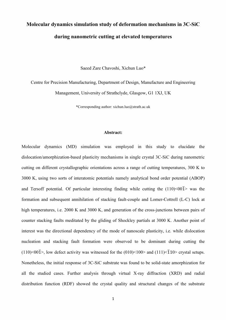
Inspired from the previous works of the authors [15-18], the same simulation model was adapted in
this study, which is shown in Fig. 1. Similar to those studies, the diamond cutting tool in this work
was modelled as a deformable body. The substrate and the cutting tool were divided into three
distinct areas namely, Newtonian, thermostat and boundary zones. Atoms in the boundary region
were kept fixed so as to reduce boundary effect and maintain lattice regularity. The simulation
model is extremely small and hence the thermostat area was used to artificially disperse the extra
heat generated within the cutting zone which in reality would have otherwise been taken away by
chips and coolant. Newtonian area follows traditional Newtonian mechanics (LAMMPS NVE
dynamics) so that the employed potential energy function decides the position of atoms as they are
integrated over time. Periodic boundary condition (PBC) was applied along the z direction. In order
to address the problem of lattice mismatch of silicon and diamond in periodic boundary condition,
the periodic box dimension was selected so that the two lattice constants were in an integer
proportion. Further description on the adjustment procedure concerning mismatch in the lattice
constant between silicon and diamond while employing PBC can be found elsewhere [19]. To keep
the simulation model simple, a major assumption here was to use the vacuum environment. This
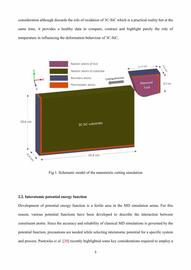
5
consideration although discards the role of oxidation of 3C-SiC which is a practical reality but at the
same time, it provides a healthy data to compare, contrast and highlight purely the role of
temperature in influencing the deformation behaviour of 3C-SiC.
Fig 1. Schematic model of the nanometric cutting simulation
2.2. Interatomic potential energy function
Development of potential energy function is a fertile area in the MD simulation arena. For this
reason, various potential functions have been developed to describe the interaction between
constituent atoms. Since the accuracy and reliability of classical MD simulations is governed by the
potential function, precautions are needed while selecting interatomic potential for a specific system
and process. Pastewka et al. [20] recently highlighted some key considerations required to employ a
6
potential energy function to model the phenomena of fracture, wear or plasticity in materials such as
silicon, carbon and silicon carbide (SiC). The most broadly adopted formalism for simulating Si-C
system is the Tersoff potential function [13], which was developed in 1994 to appropriately estimate
the ground-state structure, energies, and elastic properties of both 3C-SiC and amorphous SiC. One
decade later, Erhart and Albe [12] proposed an analytical bond order potential (ABOP) which could
describe both bulk as well as the dimer properties of SiC more properly over Tersoff potential.
Therefore, in this study, both the ABOP and Tersoff potentials were utilized to define the
interactions between the atoms of silicon and carbon and to make a comparison between the results.
2.3 Simulation procedure
MD simulations were implemented by using a public-domain computer code, known as “large-scale
atomic/molecular massively parallel simulator” (LAMMPS) [21]. The simulated cutting
temperatures were 300 K, 900 K, 1200 K, 1400 K, 2000 K and 3000 K, regulated via a Berendsen
thermostat. The details of simulation model and the process parameters employed in the simulations
are shown in Table 1.
Using improper equilibrium lattice constant will force the simulation system far away from
equilibrium and consequently the accuracy of the MD simulation results is inaccurate. Hence, the
simulation model was fed with the appropriate lattice constants shown in Table 2, which were
calculated as the equilibrium lattice constants at various temperatures from the potentials employed
in this study. The equilibrium lattice constant of diamond (cutting tool) at 300 K was computed as
3.568 Å and 3.558 Å for the ABOP and Tersoff potentials, respectively. At the start of the
simulation, the diamond tool was set at a distance of 10 Å (1 nm) from the 3C-SiC substrate (free
travel before cutting), in order to ensure that the tool atoms are far from the equilibrium cut-off
range of the Si-C interaction potential. The simulation model was equilibrated for a total time of 30
ps before the commencement of cutting. The trials were performed at a cutting speed of 50 m/s
7
since it is almost impossible to implement parametric investigations at real cutting speeds, which
are anticipated to be about 1 to 2 m/s. The visualization of atomic trajectories was carried out using
“Open Visualization Tool” (OVITO) [22] and “Dislocation Extraction Algorithm” (DXA) [14] was
employed for the sake of analysing dislocation and defects.
Table 1. Details of the MD simulation model and the cutting parameters used in the study
Substrate material Single crystal 3C-SiC
Substrate dimensions 34.8×19.6×4.4 nm3
Tool material Single crystal diamond
Cutting edge radius (tip radius) 3.5 nm
Uncut chip thickness (cutting depth in 2D) 3 nm
Cutting orientation and cutting direction Case 1: (010)<100>
Case 2: (110)<001̅>
Case 3: (111)<1̅10>
Rake and clearance angle of the cutting
tool
-25° and 10°
Substrate temperature 300 K, 900 K, 1200 K, 1400 K, 2000 K and
3000 K
Cutting speed 50 m/s
Time step 1 fs
Potential energy function ABOP [12] and Tersoff [13]
Table 2. Calculated equilibrium lattice constants and cohesive energy of single crystal 3C-SiC at
different temperatures using ABOP and Tersoff potential energy functions
Temperature (K) ABOP
lattice
constant (Å)
ABOP
cohesive
energy (eV)
Tersoff
lattice
constant
(Å)
Tersoff
cohesive
energy (eV)
Experimental
lattice constant
(Å) [23]
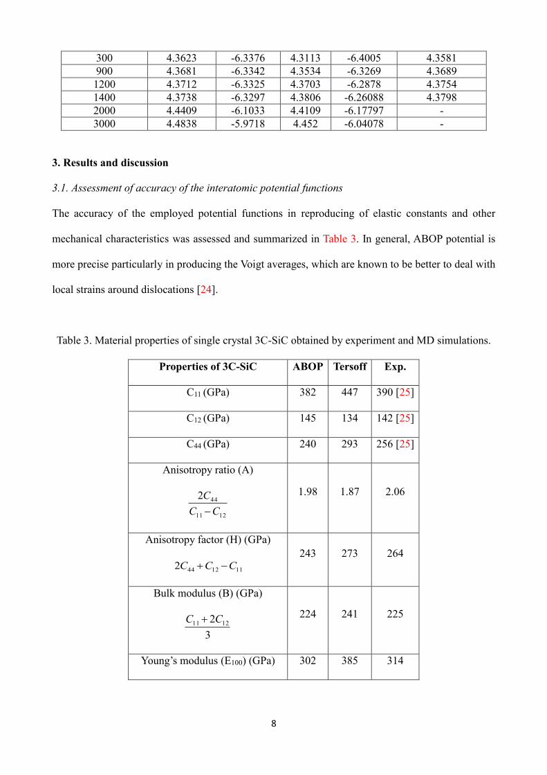
8
300 4.3623 -6.3376 4.3113 -6.4005 4.3581
900 4.3681 -6.3342 4.3534 -6.3269 4.3689
1200 4.3712 -6.3325 4.3703 -6.2878 4.3754
1400 4.3738 -6.3297 4.3806 -6.26088 4.3798
2000 4.4409 -6.1033 4.4109 -6.17797 -
3000 4.4838 -5.9718 4.452 -6.04078 -
3. Results and discussion
3.1. Assessment of accuracy of the interatomic potential functions
The accuracy of the employed potential functions in reproducing of elastic constants and other
mechanical characteristics was assessed and summarized in Table 3. In general, ABOP potential is
more precise particularly in producing the Voigt averages, which are known to be better to deal with
local strains around dislocations [24].
Table 3. Material properties of single crystal 3C-SiC obtained by experiment and MD simulations.
Properties of 3C-SiC ABOP Tersoff Exp.
C11 (GPa) 382 447 390 [25]
C12 (GPa) 145 134 142 [25]
C44 (GPa) 240 293 256 [25]
Anisotropy ratio (A)
1211
442
CC
C
1.98 1.87 2.06
Anisotropy factor (H) (GPa)
1112442 CCC 243 273 264
Bulk modulus (B) (GPa)
3
2 1211 CC
224 241 225
Young’s modulus (E100) (GPa) 302 385 314
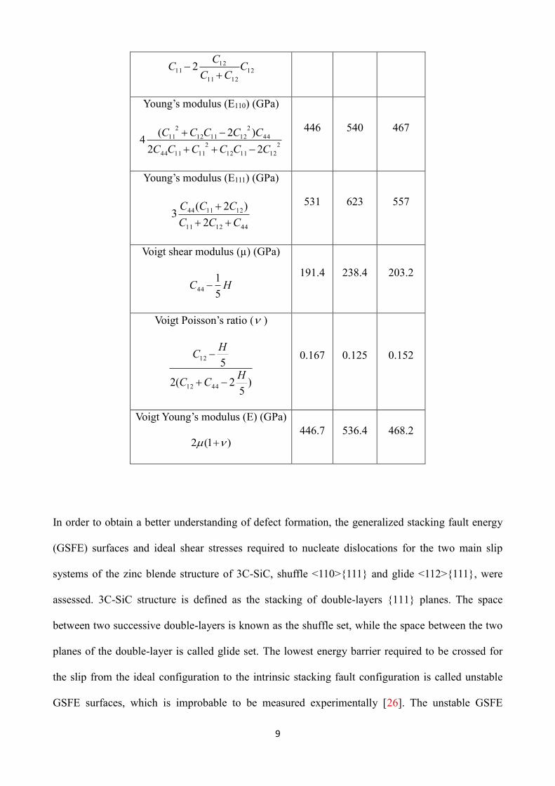
9
12
1211
1211 2 C
CC
CC
Young’s modulus (E110) (GPa)
2
121112
2
111144
44
2
121112
2
11
22
)2(4
CCCCCC
CCCCC
446 540 467
Young’s modulus (E111) (GPa)
441211
121144
2
)2(3
CCC
CCC
531 623 557
Voigt shear modulus (µ) (GPa)
HC5
144
191.4 238.4 203.2
Voigt Poisson’s ratio ( )
)5
2(2
5
4412
12
HCC
HC
0.167 0.125 0.152
Voigt Young’s modulus (E) (GPa)
)1(2 446.7 536.4 468.2
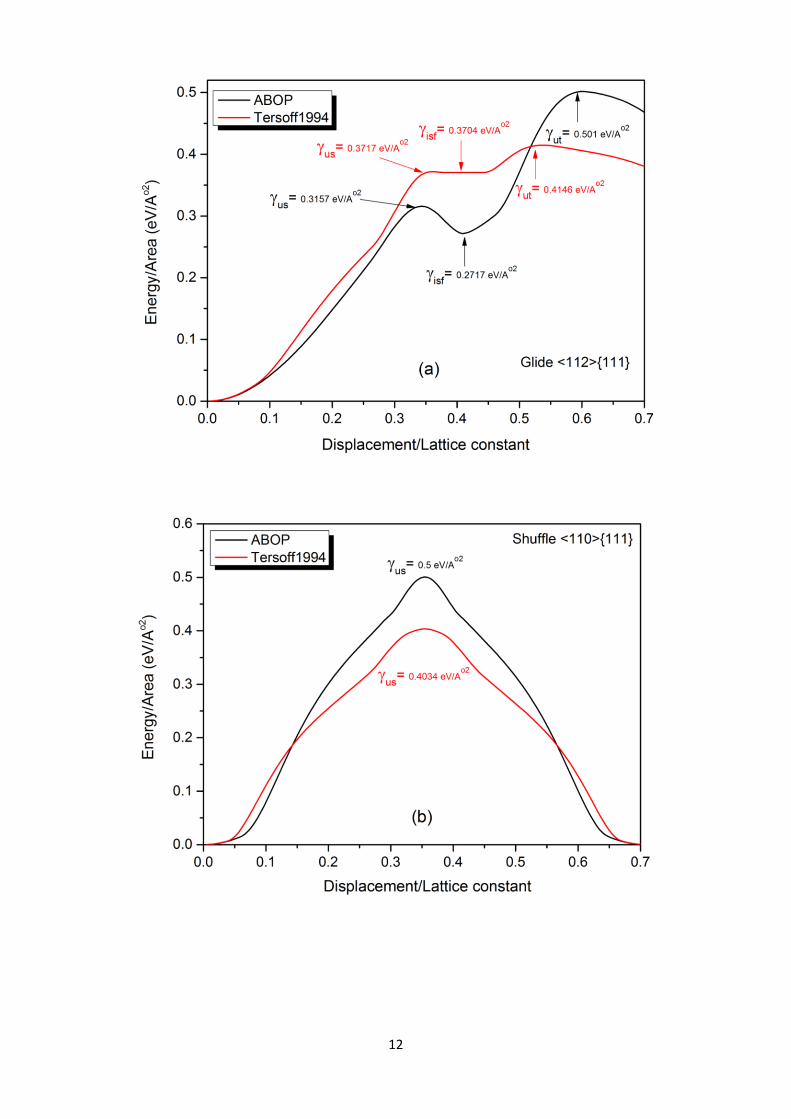
In order to obtain a better understanding of defect formation, the generalized stacking fault energy
(GSFE) surfaces and ideal shear stresses required to nucleate dislocations for the two main slip
systems of the zinc blende structure of 3C-SiC, shuffle <110>{111} and glide <112>{111}, were
assessed. 3C-SiC structure is defined as the stacking of double-layers {111} planes. The space
between two successive double-layers is known as the shuffle set, while the space between the two
planes of the double-layer is called glide set. The lowest energy barrier required to be crossed for
the slip from the ideal configuration to the intrinsic stacking fault configuration is called unstable
GSFE surfaces, which is improbable to be measured experimentally [26]. The unstable GSFE
10
surfaces can be combined with Peierls-Nabarro (PN) models [27-28] to estimate dislocation core
properties. Fig. 2a and 2b depict the GSFE curves obtained via block shearing process. Two
interatomic potentials exhibit almost similar qualitative behaviour for the shuffle and glide sets. The
unstable and intrinsic stacking fault configurations correspond to a slip of 0.342𝑎0 and 0.409𝑎0 (𝑎0
is the lattice constant), respectively, in the <112> directions. The projection of GSFE curves on the
<110> direction is symmetric corresponding to a slip of 0.353𝑎0. As seen in Fig. 2a, the value of
unstable stacking fault energy (𝛾𝑢𝑠) in the glide <112>{111} predicted by the ABOP is lower than
that of the Tersoff potential, indicative of smaller energy barrier, suggesting that dislocations can be
nucleated more easily while using the ABOP potential. It is worth pointing out here that the DFT
calculates the unstable GSFE surfaces in the glide set to be 0.1747 𝑒𝑉Å2⁄ [29-30], suggesting the
overestimation of the unstable GSFE by the two empirical potentials employed in this study.
Nevertheless, the given value by the ABOP is closer to the DFT calculation. Furthermore, the
intrinsic stacking fault energy (𝛾𝑖𝑠𝑓) for Tersoff is found much higher than that of ABOP, indicating
that the stacking faults are less likely to form while applying Tersoff potential. It is generalized that
stacking faults are common in SiC owing to the low stacking fault energy [31]. The ab initio
calculations revealed a value of 𝛾𝑖𝑠𝑓 = 0.2323 𝑒𝑉Å2⁄ [32], which is close to the magnitude given
by the ABOP (0.2717 𝑒𝑉Å2⁄ ).
It is also instructive to mention that the unstable twinning fault energy (𝛾𝑢𝑡) estimated by the ABOP
is higher than that of the Tersoff. The high ratio of 𝛾𝑢𝑡/𝛾𝑢𝑠 (~1.58) for the ABOP shows that the
energy barriers for twinning formation are higher than those for dislocation nucleation thus
twinning is difficult to form (low twinability) while utilizing this potential. However, this value for
the Tersoff is close to unity, signifying the ease of twinning formation under specific circumstances.
As for the shuffle <110>{111} slip, the predicted unstable GSFE by the Tersoff potential is lower
than that of the ABOP. The calculated unstable GSFE surface in the shuffle set by the DFT is 0.169
𝑒𝑉Å2⁄ [29-30], which is much lower than those estimated by the two potential functions. It is of
11
note that the dislocation activity is strongly subject to the crystallographic orientations of cutting
plane and cutting direction [33].
In order to obtain better insights into the favourable slip systems in our simulation setup, the
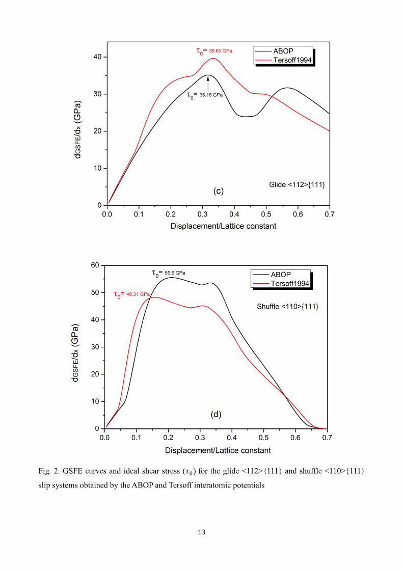
gradient of GSFE surfaces for the shuffle and glide slip systems is plotted in Fig. 2c-d. In these
plots, the maximum magnitude corresponds to the ideal shear stress (𝜏0) needed for destabilizing a
perfect crystal sheared on the shuffle <110>{111} or glide <112>{111}. Hence, 𝜏0 reflects the
critical stress required to nucleate a dislocation from a free surface in a pure crystal. As observed in
Fig. 2c-d, the ideal shear stress related to the nucleation of a dislocation on the glide set is ~35 GPa
and ~40 GPa, respectively, for the ABOP and Tersoff potentials. It appears that the ideal shear stress
in the glide set is overpredicted by both the potentials in comparison with the DFT calculations,
which is ~28 GPa [34]. On the shuffle set, the ABOP potential predicts the ideal shear stress to be
~55 GPa whereas the corresponding value estimated by the Tersoff is ~48 GPa at a shorter Burgers
vector. The ideal shear stress for the shuffle set calculated by DFT is ~37 GPa [34]. It can be
inferred that the ideal shear strength of the glide <112>{111} slip systems are lower than that of the
shuffle <110>{111}slip systems, signifying that the glide <112>{111} slip systems are more
favourable than shuffle <110>{111}slip systems. More importantly, the Schmid factor of glide slip
system is 0.47 which is larger than that of shuffle slip system, i.e. 0.41. In addition, glide
dislocations are more sensitive to thermal activation [35].
Overall, it can conclude that ABOP is more robust in predicting the mechanical properties
especially Voigt averages which are associated to the dislocations. Besides, dislocation nucleation in
the glide set and stacking fault formation given by ABOP are in better agreement with the DFT and
ab initio calculations. Hence, we report the results based on the ABOP function and whenever
needed, comparison is made with the results obtained by Tersoff potential.
12
13
Fig. 2. GSFE curves and ideal shear stress (𝜏0) for the glide <112>{111} and shuffle <110>{111}
slip systems obtained by the ABOP and Tersoff interatomic potentials
14
3.2. Analysis of crystal defects
Single crystal 3C-SiC is regarded as a face-centred cubic (FCC) crystal in the Bravais lattice group,
which simply results in multiple-slips on the four equivalent {111} planes. The preferred slip
systems are closely correlated to the core structure of their mobile dislocations. Hence, dislocations
have to glide in these planes with a trivial lattice resistance, as estimated by P-N models [27-28]. As
a starting point, we analyse the crystal defect formation when cutting is performed on the (110)
orientation since this cutting direction and cutting plane is more prone to defect formation according
to the simulation setup. Fig. 3a-b demonstrates the crystal defects at a cutting distance of 10 nm
when nanometric cutting is implemented at 300 K. The perfect dislocation loop with 1/2 < 110 >
Burgers vectors is seen to glide ahead of the tool tip. V-shaped perfect dislocation and partial half
loop are also nucleated ahead of the tool, facilitating the plasticity of 3C-SiC. Such V-shaped
dislocations were also seen by Mishra and Szlufarska [33] during sliding/cutting at a cutting depth
of 3.5 nm. Additionally, it is generalized that the non-equilibrium intrinsic point defects such as
vacancies can be created during plastic deformation process [36], leading to the formation of the
vacancy-originated stacking fault in the Si-C monolayer. So, the stacking fault observed in Fig. 3b
could be a consequence of formation of such point defects. These observations confirm that aside
from formation of one-dimensional defects, two-dimensional defects, i.e. stacking faults, can be
generated within the restricted volume of 3C-SiC substrate during nanometric cutting at room
temperature. Stacking fault formation in 3C-SiC was also observed in multimillion-atom MD
simulation of nanoindentation [37] and in thick 3C-SiC crystals grown by CF-PVT [38]. Note that
the white atoms shown in Fig. 3 represent the highly-discorded (amorphous) atoms, which have
been obtained through monitoring the local environment of atoms up to the second neighbour shell.
In Fig. 3, the chip and subsurface of substrate attain amorphous state, signifying order-disorder
(amorphization) transition of 3C-SiC atoms. The results are in accord with the simulations of Goel
et al. [39], which showed that atoms in the chip and subsurface of the substrate lose their pristine
diamond cubic lattice. Indeed, the initial response of substrate was observed to be the formation of
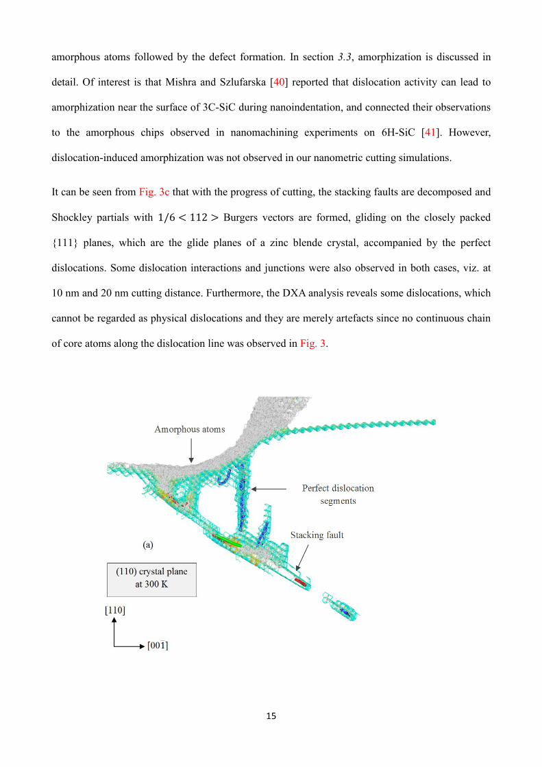
15
amorphous atoms followed by the defect formation. In section 3.3, amorphization is discussed in
detail. Of interest is that Mishra and Szlufarska [40] reported that dislocation activity can lead to
amorphization near the surface of 3C-SiC during nanoindentation, and connected their observations
to the amorphous chips observed in nanomachining experiments on 6H-SiC [41]. However,
dislocation-induced amorphization was not observed in our nanometric cutting simulations.
It can be seen from Fig. 3c that with the progress of cutting, the stacking faults are decomposed and
Shockley partials with 1/6 < 112 > Burgers vectors are formed, gliding on the closely packed
{111} planes, which are the glide planes of a zinc blende crystal, accompanied by the perfect
dislocations. Some dislocation interactions and junctions were also observed in both cases, viz. at
10 nm and 20 nm cutting distance. Furthermore, the DXA analysis reveals some dislocations, which
cannot be regarded as physical dislocations and they are merely artefacts since no continuous chain
of core atoms along the dislocation line was observed in Fig. 3.
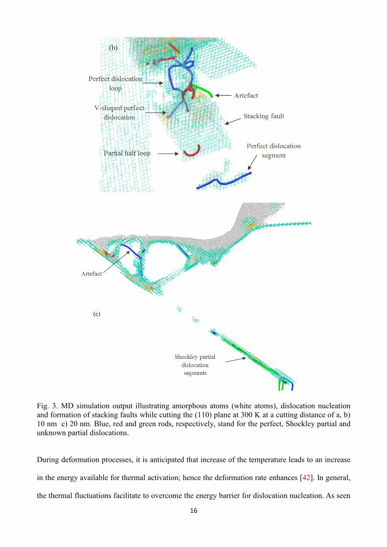
16
Fig. 3. MD simulation output illustrating amorphous atoms (white atoms), dislocation nucleation
and formation of stacking faults while cutting the (110) plane at 300 K at a cutting distance of a, b)
10 nm c) 20 nm. Blue, red and green rods, respectively, stand for the perfect, Shockley partial and
unknown partial dislocations.
During deformation processes, it is anticipated that increase of the temperature leads to an increase
in the energy available for thermal activation; hence the deformation rate enhances [42]. In general,
the thermal fluctuations facilitate to overcome the energy barrier for dislocation nucleation. As seen
17
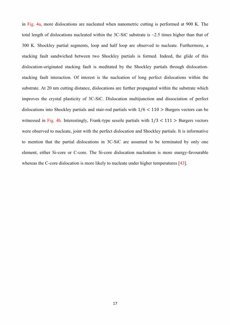
in Fig. 4a, more dislocations are nucleated when nanometric cutting is performed at 900 K. The
total length of dislocations nucleated within the 3C-SiC substrate is ~2.5 times higher than that of
300 K. Shockley partial segments, loop and half loop are observed to nucleate. Furthermore, a
stacking fault sandwiched between two Shockley partials is formed. Indeed, the glide of this
dislocation-originated stacking fault is meditated by the Shockley partials through dislocation-
stacking fault interaction. Of interest is the nucleation of long perfect dislocations within the
substrate. At 20 nm cutting distance, dislocations are further propagated within the substrate which
improves the crystal plasticity of 3C-SiC. Dislocation multijunction and dissociation of perfect
dislocations into Shockley partials and stair-rod partials with 1/6 < 110 > Burgers vectors can be
witnessed in Fig. 4b. Interestingly, Frank-type sessile partials with 1/3 < 111 > Burgers vectors
were observed to nucleate, joint with the perfect dislocation and Shockley partials. It is informative
to mention that the partial dislocations in 3C-SiC are assumed to be terminated by only one
element, either Si-core or C-core. The Si-core dislocation nucleation is more energy-favourable
whereas the C-core dislocation is more likely to nucleate under higher temperatures [43].
18
19
Fig. 4. Formation of crystal defects while cutting the (110) plane at 900 K at a cutting distance of a)
10 nm b) 20 nm. Pink and aqua rods represent the stair-rod and Frank partial dislocations.
Fig. 5a demonstrates that the defect formation mode at 1200 K is relatively similar to that of 900 K.
However, longer perfect dislocation ahead of the tool and a stacking fault beneath the tool tip can be
seen to form in this case. Phonon and thermal vibration of the atoms within the substrate rises due
to the thermal excitation, leading to an increase in the probability of having atoms with higher
energy state in the system. When the thermal energy is adequately high, there exists the possibility
of having an atom jump out of the lattice, creating a point defect in the material. The generated
point defect can lead to the formation of the vacancy-originated stacking fault. Hence, the stacking
fault observed underneath the tool tip in Fig. 5a could be a result of a point defect. Shockley partial
loops and dislocation-originated stacking fault are also nucleated. Analogous to what was observed
in Fig 3b and Fig. 4b, dislocations are multiplied continuously while cutting process advances, as
shown in Fig. 5b. Frank-type sessile partials and stair-rod partial were also witnessed to nucleate in
this case.
20
Fig. 5. Formation of crystal defects while cutting the (110) plane at 1200 K at a cutting distance of
a) 10 nm b) 20 nm
21
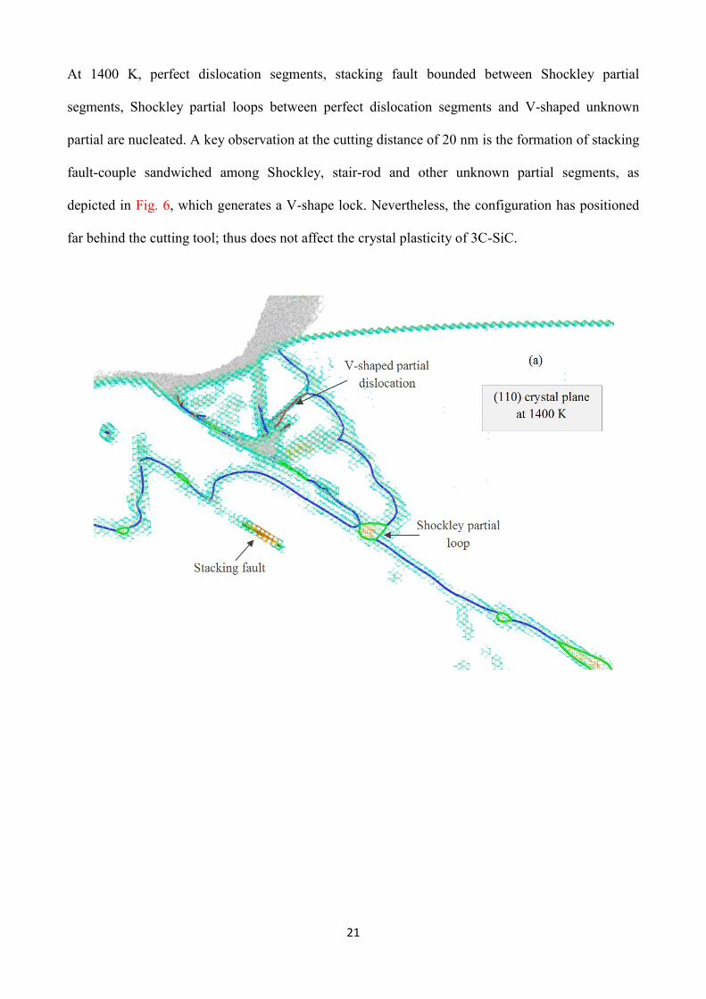
At 1400 K, perfect dislocation segments, stacking fault bounded between Shockley partial
segments, Shockley partial loops between perfect dislocation segments and V-shaped unknown
partial are nucleated. A key observation at the cutting distance of 20 nm is the formation of stacking
fault-couple sandwiched among Shockley, stair-rod and other unknown partial segments, as
depicted in Fig. 6, which generates a V-shape lock. Nevertheless, the configuration has positioned
far behind the cutting tool; thus does not affect the crystal plasticity of 3C-SiC.
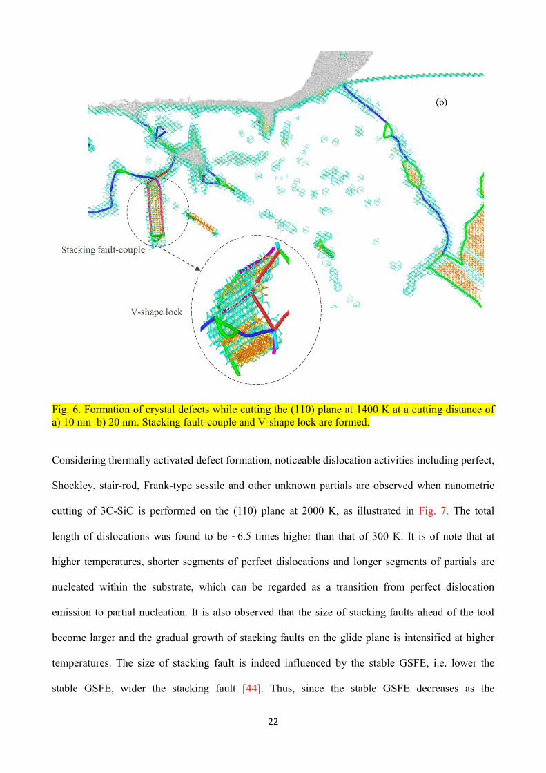
22
Fig. 6. Formation of crystal defects while cutting the (110) plane at 1400 K at a cutting distance of
a) 10 nm b) 20 nm. Stacking fault-couple and V-shape lock are formed.
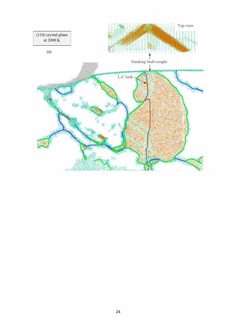
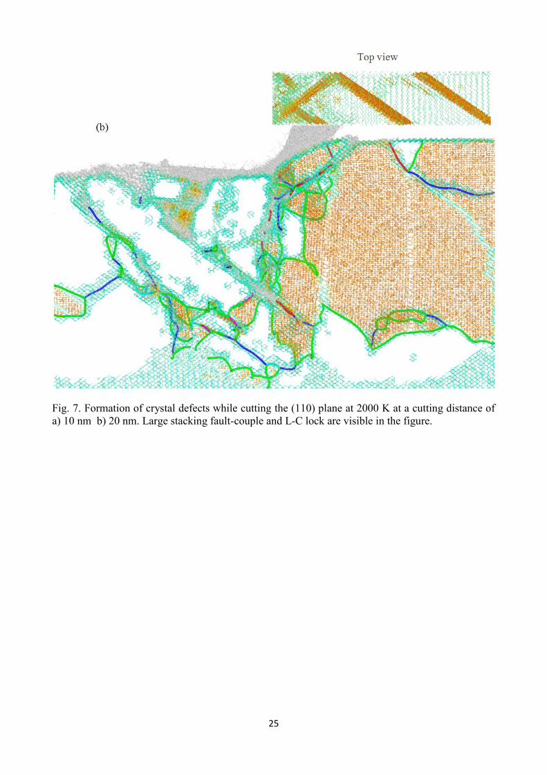
Considering thermally activated defect formation, noticeable dislocation activities including perfect,
Shockley, stair-rod, Frank-type sessile and other unknown partials are observed when nanometric
cutting of 3C-SiC is performed on the (110) plane at 2000 K, as illustrated in Fig. 7. The total
length of dislocations was found to be ~6.5 times higher than that of 300 K. It is of note that at
higher temperatures, shorter segments of perfect dislocations and longer segments of partials are
nucleated within the substrate, which can be regarded as a transition from perfect dislocation
emission to partial nucleation. It is also observed that the size of stacking faults ahead of the tool
become larger and the gradual growth of stacking faults on the glide plane is intensified at higher
temperatures. The size of stacking fault is indeed influenced by the stable GSFE, i.e. lower the
stable GSFE, wider the stacking fault [44]. Thus, since the stable GSFE decreases as the
23
temperature increases [42], wider stacking faults are observed at elevated temperatures. It has been
reported that the plastic deformation of 4H-SiC during compression loading at high temperatures is
driven by Shockley partials that bound a ribbon of stacking fault in an experimental study [45].
Since Polytypism of SiC has been reported to have a trivial effect on the dislocation core energies
and Peierls stress [46], the obtained results could be comparable with the aforementioned study.
Stacking fault-couple is also formed, which is bounded between Shockley and unknown partial
segments. These dislocations form V-shape junctions, which are typical signature of Lomer-Cottrell
(L-C) lock, arising from the interaction of dislocations on two sets of inclined {111} planes. Hence,
the combination can be recognized as an L-C lock. The bands of stacking faults form a
configuration resembling steps on a stairway. These steps are barriers to further slip on the atomic
planes involved, as well as in the adjacent planes. These arrangements, i.e. L-C lock and steps,
could culminate in the consolidation of material [47], which is analogous to what has been observed
for the low stacking fault energy metals [48]. Hence, it can be postulated that such phenomenon are
likely to happen for low stacking fault energy materials including metals and semiconductors.
Indeed, stacking fault-couple and L-C lock are supposed to be one of the primary mechanisms of
strain hardening in FCC metals with low stacking fault energy [49]. Note that with further progress
of the cutting tool, the configuration could become unlocked and L-C Lock would be annihilated.
Hence, it can be regarded as an unstable combination. In such condition, stacking faults could be
decomposed by their counterparts owing to the disconnected slip planes and thus new stacking
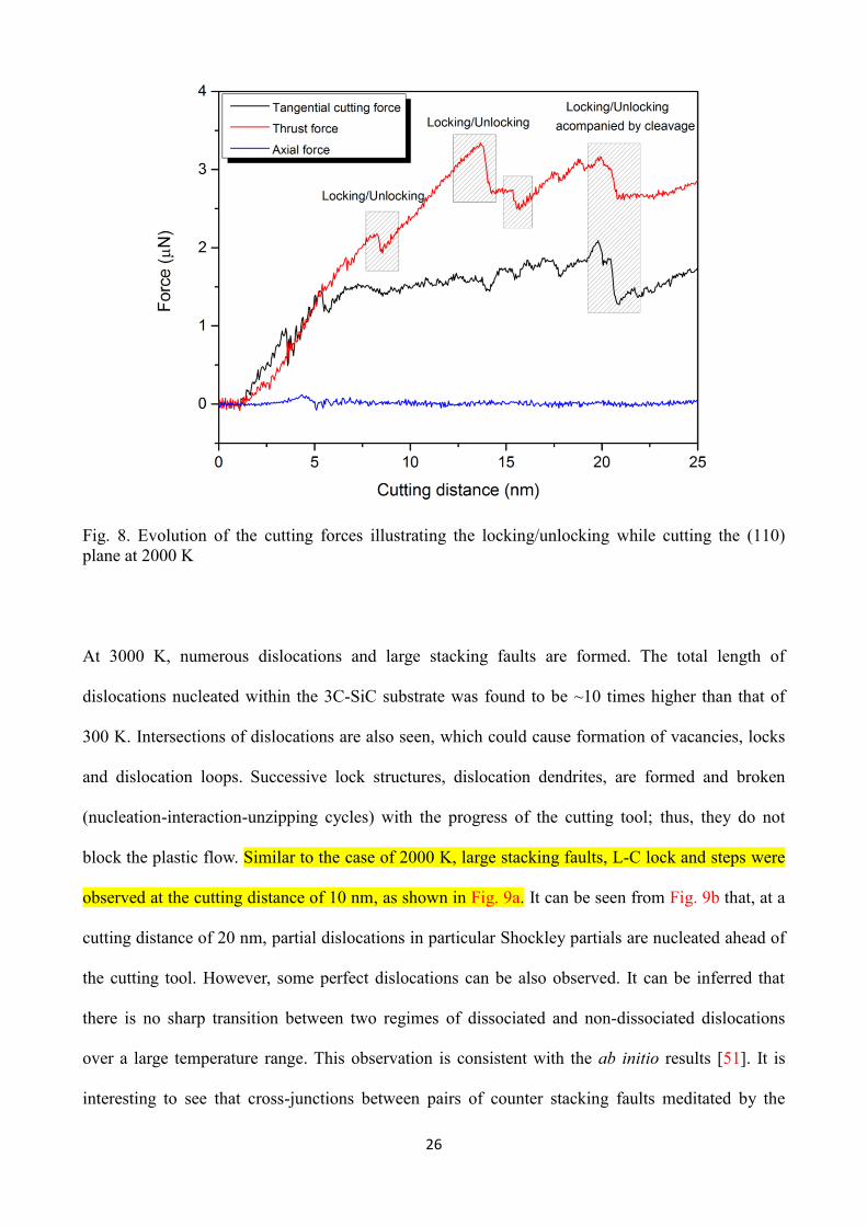
faults can be formed, as seen in Fig. 7b. As a demonstration of the occurrence of locking/unlocking
event, the evolution of cutting forces is plotted in Fig. 8. This figure provides the overall
mechanical response of 3C-SiC substrate during nanometric cutting at 2000 K. Abrupt drops in the
cutting force can be observed at the highlighted regions, indicating the unlocking process. Upon
careful examination, it was observed that the last unlocking was accompanied by the occurrence of
cleavage [50].
24
25
Fig. 7. Formation of crystal defects while cutting the (110) plane at 2000 K at a cutting distance of
a) 10 nm b) 20 nm. Large stacking fault-couple and L-C lock are visible in the figure.
26
Fig. 8. Evolution of the cutting forces illustrating the locking/unlocking while cutting the (110)
plane at 2000 K
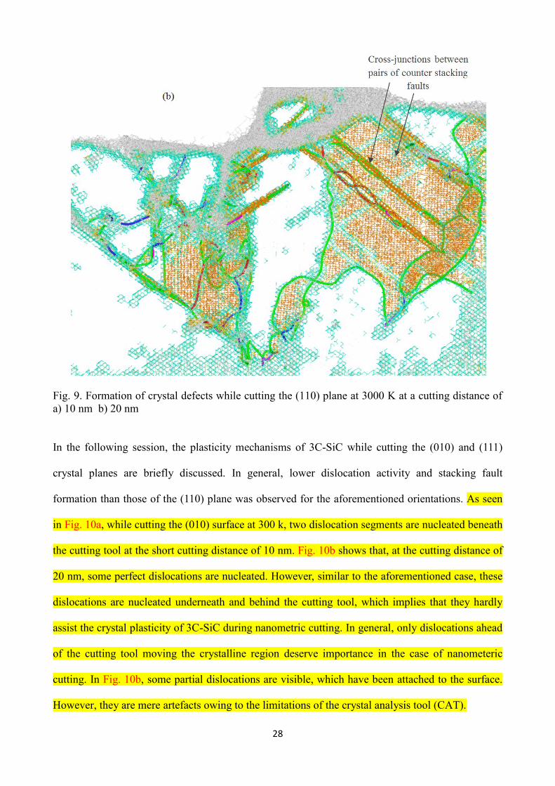
At 3000 K, numerous dislocations and large stacking faults are formed. The total length of
dislocations nucleated within the 3C-SiC substrate was found to be ~10 times higher than that of
300 K. Intersections of dislocations are also seen, which could cause formation of vacancies, locks
and dislocation loops. Successive lock structures, dislocation dendrites, are formed and broken
(nucleation-interaction-unzipping cycles) with the progress of the cutting tool; thus, they do not
block the plastic flow. Similar to the case of 2000 K, large stacking faults, L-C lock and steps were
observed at the cutting distance of 10 nm, as shown in Fig. 9a. It can be seen from Fig. 9b that, at a
cutting distance of 20 nm, partial dislocations in particular Shockley partials are nucleated ahead of
the cutting tool. However, some perfect dislocations can be also observed. It can be inferred that
there is no sharp transition between two regimes of dissociated and non-dissociated dislocations
over a large temperature range. This observation is consistent with the ab initio results [51]. It is
interesting to see that cross-junctions between pairs of counter stacking faults meditated by the

27
gliding of Shockley partials on different slip planes are formed. The intersection of counter pairs of
stacking faults could possibly create forest dislocations. This fact can be attributed to the decrease
of activation energy of dislocations with the temperature rise. Accordingly, the C-core dislocations
turn into mobile leading to the expansion of Si-terminated stacking faults. Intersection of the
counter pairs of stacking faults with each other, therefore, could result in the generation of forest
dislocations. This phenomenon could impede propagation of successive mobile dislocations.
Overall, It can be concluded that while cutting the (110) crystal plane at high temperatures, the
plasticity of 3C-SiC is mediated by large stacking faults gliding ahead of the tool tip and continuous
movement, multiplication, and entanglement of perfect and dissociated dislocations ahead,
underneath and behind of the cutting tool.
28
Fig. 9. Formation of crystal defects while cutting the (110) plane at 3000 K at a cutting distance of
a) 10 nm b) 20 nm
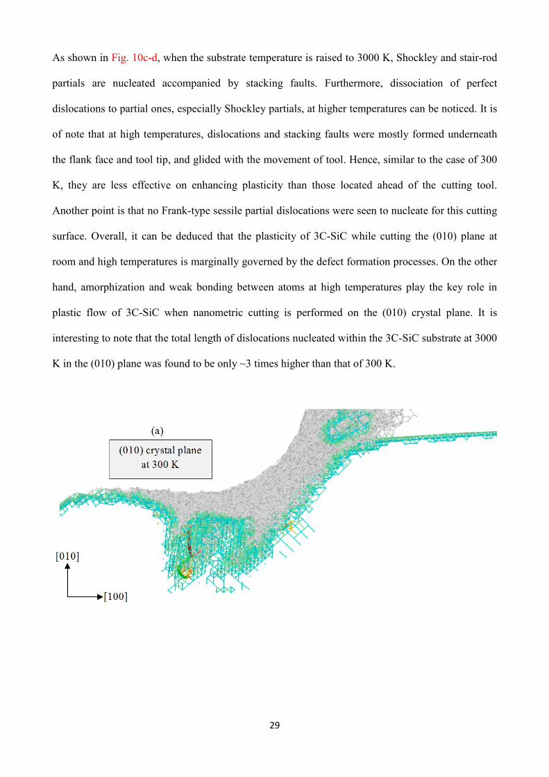
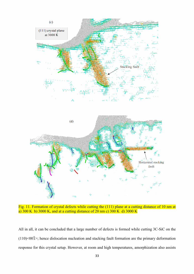
In the following session, the plasticity mechanisms of 3C-SiC while cutting the (010) and (111)
crystal planes are briefly discussed. In general, lower dislocation activity and stacking fault
formation than those of the (110) plane was observed for the aforementioned orientations. As seen
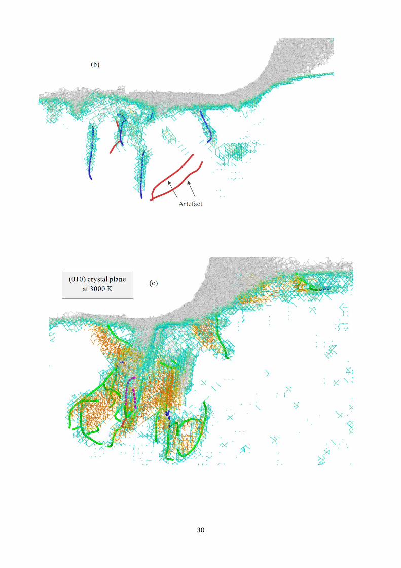
in Fig. 10a, while cutting the (010) surface at 300 k, two dislocation segments are nucleated beneath
the cutting tool at the short cutting distance of 10 nm. Fig. 10b shows that, at the cutting distance of
20 nm, some perfect dislocations are nucleated. However, similar to the aforementioned case, these
dislocations are nucleated underneath and behind the cutting tool, which implies that they hardly
assist the crystal plasticity of 3C-SiC during nanometric cutting. In general, only dislocations ahead
of the cutting tool moving the crystalline region deserve importance in the case of nanometeric
cutting. In Fig. 10b, some partial dislocations are visible, which have been attached to the surface.
However, they are mere artefacts owing to the limitations of the crystal analysis tool (CAT).
29
As shown in Fig. 10c-d, when the substrate temperature is raised to 3000 K, Shockley and stair-rod
partials are nucleated accompanied by stacking faults. Furthermore, dissociation of perfect
dislocations to partial ones, especially Shockley partials, at higher temperatures can be noticed. It is
of note that at high temperatures, dislocations and stacking faults were mostly formed underneath
the flank face and tool tip, and glided with the movement of tool. Hence, similar to the case of 300
K, they are less effective on enhancing plasticity than those located ahead of the cutting tool.
Another point is that no Frank-type sessile partial dislocations were seen to nucleate for this cutting
surface. Overall, it can be deduced that the plasticity of 3C-SiC while cutting the (010) plane at
room and high temperatures is marginally governed by the defect formation processes. On the other
hand, amorphization and weak bonding between atoms at high temperatures play the key role in
plastic flow of 3C-SiC when nanometric cutting is performed on the (010) crystal plane. It is
interesting to note that the total length of dislocations nucleated within the 3C-SiC substrate at 3000
K in the (010) plane was found to be only ~3 times higher than that of 300 K.
30
31
Fig. 10. Formation of crystal defects while cutting the (010) plane at a cutting distance of 10 nm at
a) 300 K b) 3000 K, and at a cutting distance of 20 nm c) 300 K d) 3000 K
Defect formation processes while cutting 3C-SiC on the (111) plane are shown in Fig. 11. In this
case, defects are found to be positioned ahead of the tool tip rather than underneath the cutting tool.
However, the dislocation activity while cutting the (111) surface is seen to be low at short cutting
distances, i.e. 10 nm, as illustrated in Fig. 11a, as opposed to the (110) crystal plane. With the
progress of cutting, more dislocations are nucleated ahead of the tool, as shown in Fig. 11b. At
higher temperatures i.e. 3000 K, dislocation nucleation and stacking fault formation were observed
at short cutting distances. An interesting observation was the formation of horizontal stacking fault
at high temperatures of 2000 K and 3000 K at the cutting distance of 20 nm, as shown in Fig. 11d.
Also, Frank-type sessile partial dislocation was seen to nucleate as opposed to the (010) plane. The
total length of dislocations nucleated within the 3C-SiC substrate at 3000 K was found to be ~4
times higher than that of 300 K.
32
33
Fig. 11. Formation of crystal defects while cutting the (111) plane at a cutting distance of 10 nm at
a) 300 K b) 3000 K, and at a cutting distance of 20 nm c) 300 K d) 3000 K
All in all, it can be concluded that a large number of defects is formed while cutting 3C-SiC on the
(110)<001̅>; hence dislocation nucleation and stacking fault formation are the primary deformation
response for this crystal setup. However, at room and high temperatures, amorphization also assists
34
the plasticity of 3C-SiC. Overall, the initial response of substrate in all the studied cases was the
formation of disordered (amorphous) atoms thus it can be generalized that the incipient plasticity of
3C-SiC in nanometric cutting occurs by solid-state amorphization. In addition, at high temperatures,
the amplitude of atomic vibration of the substrate atoms increases, which is regarded as an increase
in the number of phonons. This phenomenon results in generating atomic displacements. The
atomic displacements within the substrate causes an increase in the interatomic distances and a
decrease in the restoring forces due to thermal expansion, which lowers the energy required to break
the atomic bonds. As a consequence, deformation of 3C-SiC at high temperatures is facilitated.
When nanometric cutting is performed on the (010)<100> orientation setup at room and high
temperatures, the plasticity of 3C-SiC is marginally governed by the defect formation processes.
Thus, the plasticity is primarily meditated by amorphization and weak bonding between atoms at
high temperatures. With the (111)<1̅10> setup, room temperature plasticity at short cutting
distances is mainly governed by the amorphization whereas at long distances, dislocation nucleation
also assists the plastic deformation of 3C-SiC. At higher temperatures, the plasticity of 3C-SiC on
the (111) plane is meditated by the defect formation, as well as the amorphization and weak
bonding between atoms. It should be also noted that at higher temperatures a small number of stair-
rod and Frank-type sessile partials are observed to nucleate while cutting 3C-SiC on the different
crystal planes.
It is instructive to note that in the cases where the Tersoff potential were applied, no stacking fault
formation was observed, attributable to the high stacking fault energy given by this potential, as
calculated in Section 3.1. In addition, very low dislocation activity was observed while applying
Tersoff potential. For instance, while cutting 3C-SiC on the (010) and (111) planes in the
temperature range of 900 K to 3000 K, no dislocation was nucleated. In the case of (110)
orientation, a low density of dislocations was observed at temperatures higher than 900 K.
35
3.3. Structural changes
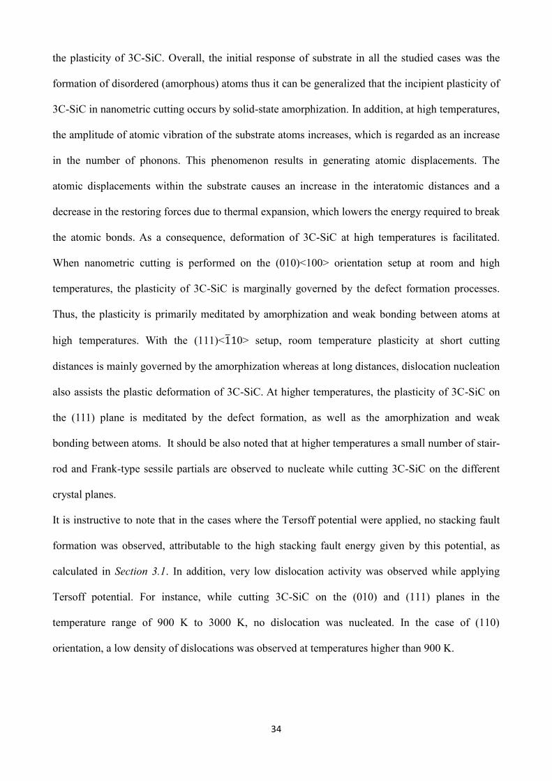
To obtain better insights about structural changes of the zinc blende structure, the radial distribution
function g(r) before and after nanometric cutting of 3C-SiC at elevated temperatures are plotted.
The radial distribution function (RDF), or pair distribution function, is regarded as the major
connection between macroscopic thermodynamic characteristics and interatomic activities. It can be
seen from Fig. 12 that various peaks occur in the RDF for each individual cutting temperature. The
bond length at the peaks has a small discrepancy. The first three peaks of RDF correspond to C-Si,
C-C and C-Si bonds relative to the equilibrium bond lengths of 1.88 Å, 3.08 Å and 3.62 Å,
respectively, as shown in Fig. 12. Evidently, the peaks become weaker as temperature of the
substrate increases, which is an indication of increased amplitude of atomic vibrations and
corresponding atomic displacements from their original equilibrium positions. Apart from the
peaks, the bond length increases with the increase of temperature, representing the enhanced
structural changes and consequently superior plasticity of 3C-SiC before and during the cutting. An
interesting observation from Fig 12 is the growth of an embryo peak at the interatomic distance of
1.45 Å, which is the equilibrium bond length of C-C, signifying the formation of C-C bond. It
should be noted here that the analogous qualitative trend was observed for the three crystal planes.
36
Fig. 12. Radial distribution function showing interatomic bond lengths at different temperatures
before and after nanometric cutting on the (010) crystal surface.
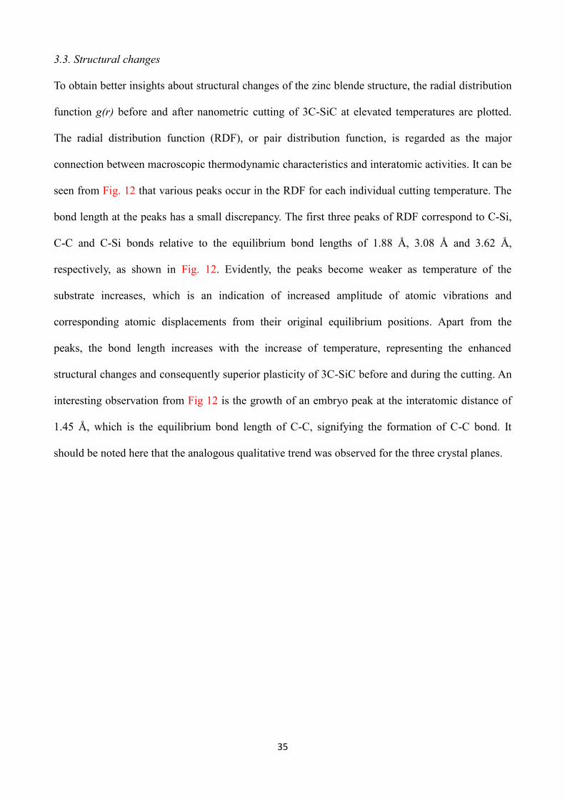
As mentioned in Section 3.2, the white atoms in the cutting chip and subsurface of substrate
presented in Figs. 3-7 and 9-11 have experienced the transition to a disordered state, a phenomenon
known as solid-state amorphization [52]. In order to further characterize the crystal qualities of 3C-
SiC substrate during nanometric cutting, virtual X-ray diffraction (XRD) [53] with Cu Kα radiation
(1.5418 Å) was carried on an elemental atomic volume (3×3×3 nm3 including 2552 atoms) in the
cutting region. The XRD spectrums obtained from the simulations are illustrated in Fig. 13. Peaks
at 2θ value of 35.96°, 40.38°, 55.13° and 76.19° shown in Fig. 13a correspond to the crystalline 3C-
SiC, which is consistent with the standard XRD pattern of 3C-SiC powders displayed in Fig. 13d
[54]. Note that a small amount of mismatch in peak position is commonly acceptable. The
prominent peak at 2θ=35.96° is diffracted from 3C-SiC (111) according to the database of joint
committee on powder diffraction standards (JCPDS). The second, third and fourth ones are
diffracted form 3C-SiC (200), (220) and (311), respectively. It can be seen from Fig. 13b that, after
cutting, both relative intensities and number of the diffraction peaks alter noticeably, and several
37
new diffractions appear. The peaks possess lower relative intensities, particularly the strong peaks
shown in Fig. 13a almost disappear, signifying the amorphization of atoms in the cutting
deformation zone owing to the large shear stresses and plastic strains. Note that an increase in the
intensity of 3C-SiC (200) can be seen. However, due to the fact that Si and C atoms have ionicity so
the local crystal structures are not simple like elements. Hence, it is very challenging to bring a
specific reason for this observation.
Fig. 13c shows the XRD profile of 3C-SiC during the cutting, a mixture of crystalline and
amorphous atoms in the cutting region, where the pattern could be assumed as a combination of
crystalline and amorphous XRD spectra observed in Fig. 13a and 13b. It can be found from Fig. 13c
that the intensity maxima of 3C-SiC (111) at 2θ=35.96° is approximately 3.8 times lower than that
of the crystalline 3C-SiC, indicating an inferior crystal quality in presence of both crystalline and
amorphous structure in the cutting region.

38
Fig. 13. XRD spectrum of 3C-SiC in the cutting region a) before b) after and c) during nanometric
cutting on the (010) crystal surface. d) Standard XRD pattern of 3C-SiC powders
It should be mentioned here that the available bond order potential (BOP) functions, including
ABOP and Tersoff potentials, are not robust in describing and capturing all the structural phases as
they are not able to properly resolve competing mechanisms involving subtle influences of chemical
bonding, i.e. ionic bonding. Thus, phase transformation mechanisms cannot be realized using BOP
potentials. It is instructive to note that there has been a long debate on the possibility of
polymorphic transition to another lattice structure during contact loading of SiC polytypes. Such
mechanism has been proposed from experimental studies on 3C-SiC [55]; however, in almost all
MD studies no direct evidence has been presented. Instead, indirect observation has been reported,
meaning that if SiC undergoes a local pressure as high as 100 GPa then the transformation to
rocksalt structure would take place [56]. Nevertheless, Mishra and Szlufarska [40] have shown that,
using Vashishta et al’s. potential function [29] which has been reported to be more accurate for
describing the high pressure phase transformation of SiC, even under the local atomic pressures as
high as 100 GPa, the polymorphic transition does not occur in SiC. The only direct observation of
phase transformation in MD simulation was provided by Xiao et al. [57], where very small amount
of atoms were seen to undergo phase transition from 6H-SiC to rocksalt structure. However, more
39
evidence is needed to be able to generalize occurrence of the phase transition at a strictly nanometre
level in MD trials. Hence, polymorphic transition is still a hypothesis for the deformation
mechanisms of SiC in MD simulation, in contrast to silicon where phase transformation has been
witnessed [58]. However, defect-free specimen employed in MD simulation might play a role in
hindering the occurrence of such transition in MD simulations of SiC.
3.4. Yielding stresses
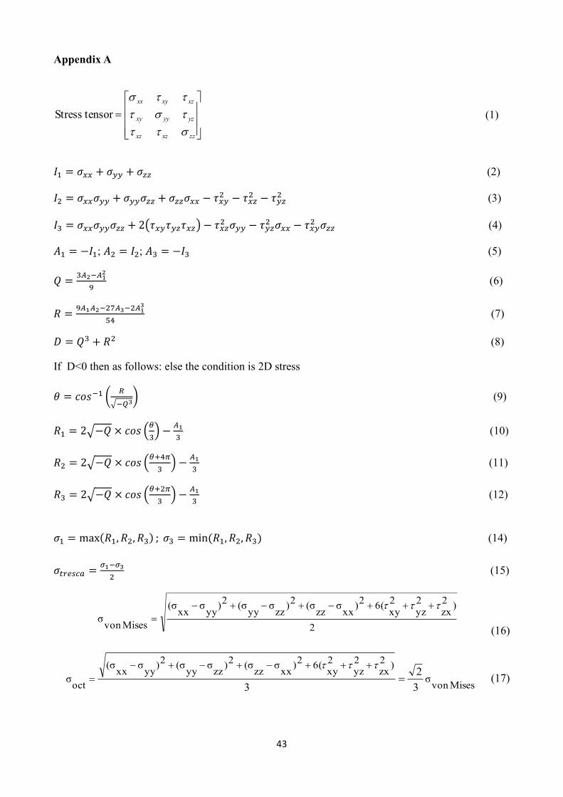
Material dependent yielding criteria such as von Mises stress, Principal stress and Tresca stress
measures were employed to predict yielding of 3C-SiC under various circumstances in this study. In
order to compute the atomic stress tensor1, an elemental atomic volume (1×1.5×3 nm3 including
442 atoms) was considered in the cutting region and accordingly the physical stress tensor was
obtained. Equations shown in Appendix A were adopted to calculate the aforementioned yielding
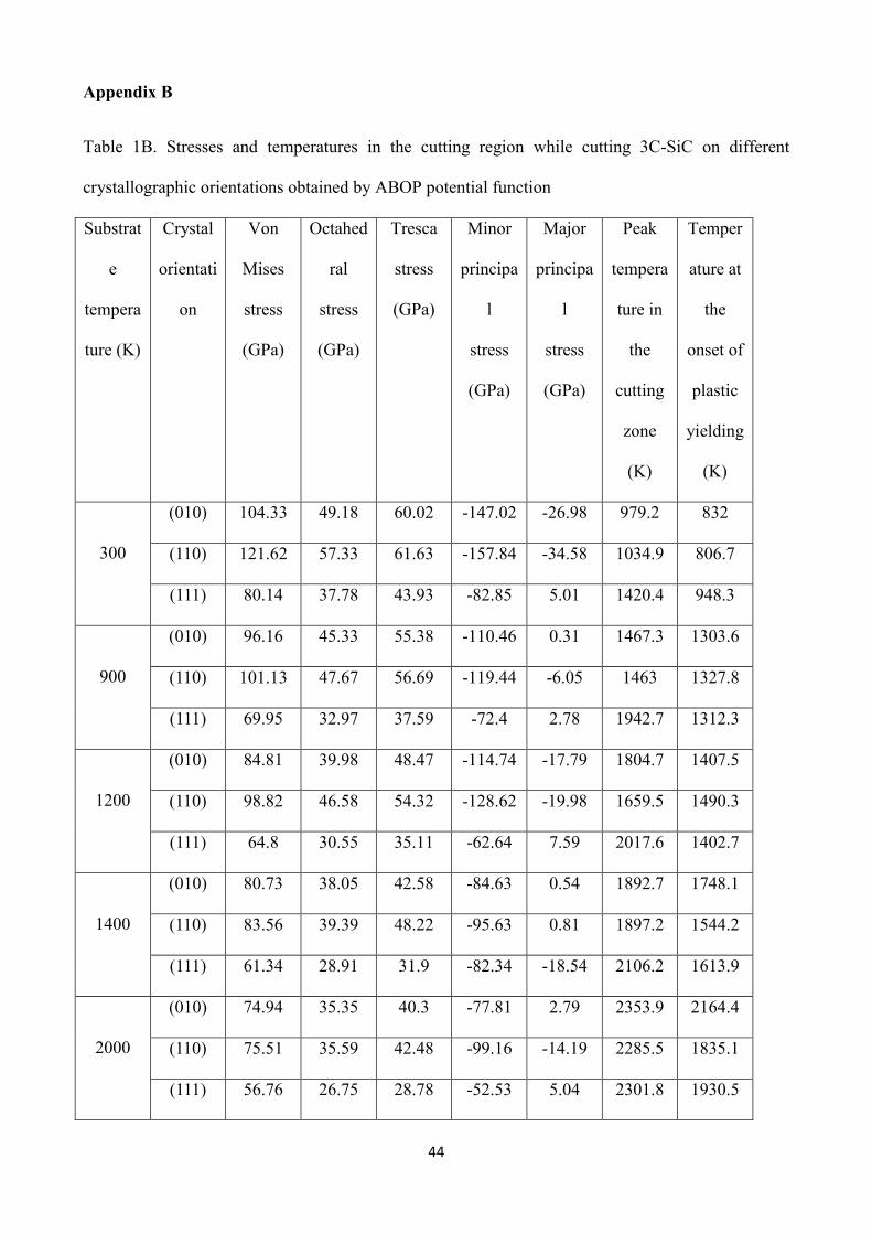
measures. Table 1B in Appendix B summarizes the magnitude of all the stresses obtained from the
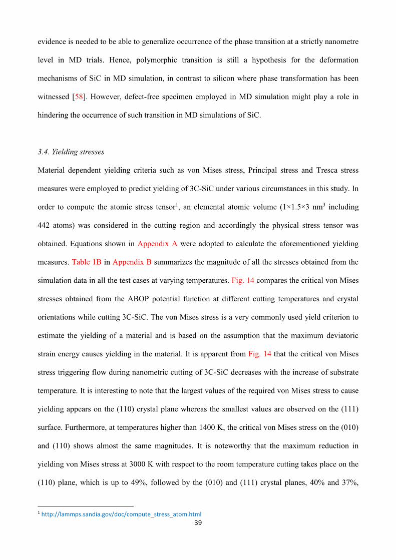
simulation data in all the test cases at varying temperatures. Fig. 14 compares the critical von Mises
stresses obtained from the ABOP potential function at different cutting temperatures and crystal
orientations while cutting 3C-SiC. The von Mises stress is a very commonly used yield criterion to
estimate the yielding of a material and is based on the assumption that the maximum deviatoric
strain energy causes yielding in the material. It is apparent from Fig. 14 that the critical von Mises
stress triggering flow during nanometric cutting of 3C-SiC decreases with the increase of substrate
temperature. It is interesting to note that the largest values of the required von Mises stress to cause
yielding appears on the (110) crystal plane whereas the smallest values are observed on the (111)
surface. Furthermore, at temperatures higher than 1400 K, the critical von Mises stress on the (010)
and (110) shows almost the same magnitudes. It is noteworthy that the maximum reduction in
yielding von Mises stress at 3000 K with respect to the room temperature cutting takes place on the
(110) plane, which is up to 49%, followed by the (010) and (111) crystal planes, 40% and 37%,
1 http://lammps.sandia.gov/doc/compute_stress_atom.html
40
respectively.
Fig. 14. Variation of critical von Mises stress in the cutting region while cutting 3C-SiC on different
crystal planes and at different temperatures obtained by ABOP potential function
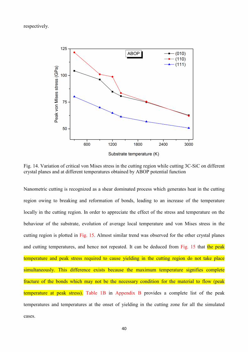
Nanometric cutting is recognized as a shear dominated process which generates heat in the cutting
region owing to breaking and reformation of bonds, leading to an increase of the temperature
locally in the cutting region. In order to appreciate the effect of the stress and temperature on the
behaviour of the substrate, evolution of average local temperature and von Mises stress in the
cutting region is plotted in Fig. 15. Almost similar trend was observed for the other crystal planes
and cutting temperatures, and hence not repeated. It can be deduced from Fig. 15 that the peak
temperature and peak stress required to cause yielding in the cutting region do not take place
simultaneously. This difference exists because the maximum temperature signifies complete
fracture of the bonds which may not be the necessary condition for the material to flow (peak
temperature at peak stress). Table 1B in Appendix B provides a complete list of the peak
temperatures and temperatures at the onset of yielding in the cutting zone for all the simulated
cases.
41
Fig. 15. Evolution of the temperature and von Mises stress in the cutting region recorded on the
same plot while cutting 3C-SiC on the (111) crystal plane at 1200 K
4. Concluding remarks
This work made use of the MD simulation to deal with the nanoscale plasticity of single crystal 3C-
SiC during nanometric cutting on different crystallographic orientations at a range of temperature
(from 300 K to 3000 K) using two potential energy functions, i.e. ABOP and Tersoff.
Complimentary calculations of mechanical properties, GSFE surfaces and ideal shear stresses lend
further credence to the reported findings. Based on the aforementioned results, conclusions can be
drawn as:
1. Successive formation and destruction of stacking fault-couple bounding between partial
dislocation segments and Lomer-Cottrell (L-C) lock were observed while cutting 3C-SiC on
the (110)<001̅> orientation setup at high temperatures. Furthermore, cross-junctions
42
between pairs of counter stacking faults meditated by the gliding of Shockley partials on
different slip planes were formed at 3000 K for the aforementioned crystal setup.
2. Dislocation multi-junction, Frank-type sessile and stair-rod partials were observed to
nucleate at substrate temperatures 𝑇 ≥ 900 𝐾 when cutting was performed on the (110)
surface.
3. Dislocation nucleation and stacking fault formation were observed to be dominant during
cutting the (110)<001̅> crystal setup. However, low defect activity was seen for the
(010)<100> and (111)<1̅10> crystal setups. More importantly, the incipient plasticity of 3C-
SiC in nanometric cutting was observed to occur by solid-state amorphization.
4. Substantial difference was observed in both the relative intensities and number of the
diffraction peaks of the virtual XRD spectrums before and after cutting, signifying the
amorphization of atoms in the cutting deformation region. In addition, the peaks in RDF
became weaker and bond length was seen to increase as substrate temperature increased or
after cutting.
5. The maximum reduction in yielding stresses with respect to the increase of cutting
temperature occurred on the (110) crystal plane.
Acknowledgment
The authors gratefully acknowledge the financial support from the EPSRC (EP/K018345/1) and
Royal Society-NSFC international exchange programme (IE141422) for this study. The authors also
acknowledge the use of the EPSRC (EP/K000586/1) funded ARCHIE-WeSt High Performance
Computer at the University of Strathclyde. The first author (SZC) also acknowledges the help of Dr.
Saurav Goel from Queen’s University, Belfast, UK and Dr. Alexander Stukowski from TU
Darmstadt, Germany for their useful advice.
43
Appendix A
zzxzxz
yzyyxy
xzxyxx
tensorStress (1)
𝐼1 = 𝜎𝑥𝑥 + 𝜎𝑦𝑦 + 𝜎𝑧𝑧 (2)
𝐼2 = 𝜎𝑥𝑥𝜎𝑦𝑦 + 𝜎𝑦𝑦𝜎𝑧𝑧 + 𝜎𝑧𝑧𝜎𝑥𝑥 − 𝜏𝑥𝑦2 − 𝜏𝑥𝑧
2 − 𝜏𝑦𝑧2 (3)
𝐼3 = 𝜎𝑥𝑥𝜎𝑦𝑦𝜎𝑧𝑧 + 2(𝜏𝑥𝑦𝜏𝑦𝑧𝜏𝑥𝑧) − 𝜏𝑥𝑧2 𝜎𝑦𝑦 − 𝜏𝑦𝑧
2 𝜎𝑥𝑥 − 𝜏𝑥𝑦2 𝜎𝑧𝑧 (4)
𝐴1 = −𝐼1; 𝐴2 = 𝐼2; 𝐴3 = −𝐼3 (5)
𝑄 =3𝐴2−𝐴1
2
9 (6)
𝑅 =9𝐴1𝐴2−27𝐴3−2𝐴1
3
54 (7)
𝐷 = 𝑄3 + 𝑅2 (8)
If D<0 then as follows: else the condition is 2D stress
𝜃 = 𝑐𝑜𝑠−1 (𝑅
√−𝑄3) (9)
𝑅1 = 2√−𝑄 × 𝑐𝑜𝑠 (𝜃
3) −
𝐴1
3 (10)
𝑅2 = 2√−𝑄 × 𝑐𝑜𝑠 (𝜃+4𝜋
3) −
𝐴1
3 (11)
𝑅3 = 2√−𝑄 × 𝑐𝑜𝑠 (𝜃+2𝜋
3) −
𝐴1
3 (12)
𝜎1 = max(𝑅1, 𝑅2, 𝑅3) ; 𝜎3 = min (𝑅1, 𝑅2, 𝑅3) (14)
𝜎𝑡𝑟𝑒𝑠𝑐𝑎 =𝜎1−𝜎3
2 (15)
2
)2zx
2yz
2xy
6(2
)xxσ
zz(σ
2)
zzσ
yy(σ
2)
yyσ
xx(σ
Misesvonσ
(16)
Misesvonσ
)2zx
2yz
2xy
6(2
)xxσ
zz(σ
2)
zzσ
yy(σ
2)
yyσ
xx(σ
octσ
3
2
3
(17)
44
Appendix B
Table 1B. Stresses and temperatures in the cutting region while cutting 3C-SiC on different
crystallographic orientations obtained by ABOP potential function
Substrat
e
tempera
ture (K)
Crystal
orientati
on
Von
Mises
stress
(GPa)
Octahed
ral
stress
(GPa)
Tresca
stress
(GPa)
Minor
principa
l
stress
(GPa)
Major
principa
l
stress
(GPa)
Peak
tempera
ture in
the
cutting
zone
(K)
Temper
ature at
the
onset of
plastic
yielding
(K)
300
(010) 104.33 49.18 60.02 -147.02 -26.98 979.2 832
(110) 121.62 57.33 61.63 -157.84 -34.58 1034.9 806.7
(111) 80.14 37.78 43.93 -82.85 5.01 1420.4 948.3
900
(010) 96.16 45.33 55.38 -110.46 0.31 1467.3 1303.6
(110) 101.13 47.67 56.69 -119.44 -6.05 1463 1327.8
(111) 69.95 32.97 37.59 -72.4 2.78 1942.7 1312.3
1200
(010) 84.81 39.98 48.47 -114.74 -17.79 1804.7 1407.5
(110) 98.82 46.58 54.32 -128.62 -19.98 1659.5 1490.3
(111) 64.8 30.55 35.11 -62.64 7.59 2017.6 1402.7
1400
(010) 80.73 38.05 42.58 -84.63 0.54 1892.7 1748.1
(110) 83.56 39.39 48.22 -95.63 0.81 1897.2 1544.2
(111) 61.34 28.91 31.9 -82.34 -18.54 2106.2 1613.9
2000
(010) 74.94 35.35 40.3 -77.81 2.79 2353.9 2164.4
(110) 75.51 35.59 42.48 -99.16 -14.19 2285.5 1835.1
(111) 56.76 26.75 28.78 -52.53 5.04 2301.8 1930.5
45
3000
(010) 62.68 29.55 36.02 -66.76 5.28 3395.6 2590.1
(110) 62.17 29.31 34.87 -80.34 -10.59 3267.5 2527.6
(111) 50.71 23.9 26.36 -49.88 2.85 3230 2565.3
References
[1] S. Goel, The current understanding on the diamond machining of silicon carbide. J. Phys. D:
Appl. Phys. 47 (2014) 243001
[2] M. Yoshida et al, Pressure-induced phase transition in SiC. Phys. Rev. B 48 (1993) 10587-90
[3] F. Shimojo et al, Molecular dynamics simulation of structural transformation in silicon carbide
under pressure. Phys. Rev. Lett. 84 (2000) 3338
[4] M. Tang, Elastic instabilities and structural responses of Beta-SiC under stress PhD Thesis
Massachusetts Institute of Technology, Cambridge, MA (1995).
[5] A. Noreyan A, J. G. Amar, I. Marinescu, Molecular dynamics simulations of nanoindentation of
beta-SiC with diamond indenter. Mater. Sci. Eng. B 117 (2005) 235-40
[6] I. Szlufarska, R. K. Kalia, A. Nakano, P. Vashishta, Atomistic mechanisms of amorphization
during nanoindentation of SiC: a molecular dynamics study. Phys. Rev. B 71 (2005) 174113
[7] M. Mishra, I. Szlufarska, Possibility of high-pressure transformation during nanoindentation of
SiC. Acta Mater. 57 (2009) 6156-65
[8] J-L. Demenet et al, Dislocations in 4H- and 3C-SiC single crystals in the brittle regime Phys.
Status Solidi c10 (2013) 64-7
[9] X. Zhao et al, Onset plastic deformation and cracking behaviour of silicon carbide under contact
load at room temperature J. Am. Ceram. Soc. 94 (2011) 3509-14
46
[10] S. Goel, X. Luo, R. L. Reuben, Shear instability of nanocrystalline silicon carbide during
nanometric cutting Appl. Phys. Lett. 100 (2012) 231902
[11] M. Mishra, I. Szlufarska, Dislocation controlled wear in single crystal silicon carbide J. Mater.
Sci. 48 (2013) 1593-603
[12] P. Erhart, K. Albe, Analytical potential for atomistic simulations of silicon, carbon, and silicon
carbide. Physical Review B, 71(3) (2005) 035211
[13] Tersoff, J., Chemical order in amorphous silicon carbide. Physical Review B, 49 (23) (1994)
16349
[14] A. Stukowski, K. Albe, Extracting dislocations and non-dislocation crystal defects from
atomistic simulation data. Modelling Simul. Mater. Sci. Eng. 18 (2010) 085001
[15] S. Z. Chavoshi, S. Goel, X. Luo, Molecular dynamics simulation investigation on plastic flow
behaviour of silicon during nanometric cutting. Modelling Simul. Mater. Sci. Eng. 24 (2016)
015002
[16] S. Z. Chavoshi, S. Goel, X. Luo, Influence of temperature on the anisotropic cutting behaviour
of single crystal silicon: A molecular dynamics simulation investigation. Submitted for publication
[17] S. Z. Chavoshi, X. Luo, Defect mediated plasticity in silicon during nanometric cutting: A
molecular dynamics simulation study. Submitted for publication
[18] S. Z. Chavoshi, X. Luo, An atomistic simulation investigation on chip related phenomena in
nanometric cutting of single crystal silicon at elevated temperatures. Computational Materials
Science, (2015) doi:10.1016/j.commatsci.2015.11.027
[19] S. Goel, X. Luo, A. Agrawal, R. L. Reuben, Diamond machining of silicon: A review of
advances in molecular dynamics simulation, International Journal of Machine Tools & Manufacture
88 (2015) 131-164
47
[20] L. Pastewka, A. Klemenz, P. Gumbsch, M. Moseler, Screened empirical bond-order potentials
for Si-C. Phys. Rev. B 87 (2013) 205410
[21] S. Plimpton, Fast parallel algorithms for short-range molecular-dynamics. Journal of
computational physics, 117 (1) (1995) 1-19
[22] A. Stukowski, Visualization and analysis of atomistic simulation data with OVITO-the Open
Visualization Tool Modelling Simul. Mater. Sci. Eng. 18 (2010), 015012
[23] Z. Li, R. C. Bradt, Thermal expansion of the cubic (3C) polytype of SiC. Journal of Materials
Science 21 (1986) 4366-4368
[24] R. Hull, Properties of Crystalline Silicon. INSPEC publication (1999)
[25] W. R. L. Lambrecht, B. Segall, M. Methfessel, M. van Schilfgaarde, Calculated elastic
constants and deformation potentials of cubic SiC. Phys. Rev. B 44 (1991) 3685
[26] H. V. Swygenhoven, P. M. Derlet, A. G. Frøseth, Stacking fault energies and slip in
nanocrystalline metals. Nature Mater. 3, (2004) 399-403
[27] R. Peierls, The size of a dislocation. Proc. Phys. Soc. 52 (1940) 34-37
[28] F. R. N. Nabarro, Dislocations in a simple cubic lattice. Proc. Phys. Soc. 59 (1947) 256-272
[29] P. Vashishta, R. K. Kalia, A. Nakano, J. P. Rino, Interaction potential for silicon carbide: A
molecular dynamics study of elastic constants and vibrational density of states for crystalline and
amorphous silicon carbide. Journal of applied physics 101 (2007) 103515
[30] T. Thomas, D. Pandey, U. V. Waghmare, Soft modes at the stacking faults in SiC crystals:
First-principles calculations. Physical Review B 77, 121203 (R) (2008)
[31] G. Cheng, T-H Chang, Qi. Qin, H. Huang, Y. Zhu, Mechanical Properties of Silicon Carbide
Nanowires: Effect of Size- Dependent Defect Density. Nano Lett. 2014, 14, 754-758
48
[32] Y. Umeno, K. Yagi, H. Nagasawa, ab initio density functional theory calculation of stacking
fault energy and stress in 3C-SiC. Phys. Status Solidi B 249 (6) (2012) 1229-1234
[33] M. Mishra, I. Szlufarska, Dislocation controlled wear in single crystal silicon carbide. J Mater
Sci 48 (2013) 1593-1603
[34] Y. Umeno, Y. Kinoshita, T. Kitamura, Ab initio DFT simulation of ideal shear deformation of
SiC polytypes. Modelling Simul. Mater. Sci. Eng. 15 27 (2007)
[35] L. Kubin, Dislocations, Mesoscale Simulations and Plastic Flow. Oxford publication, ISBN-13:
9780198525011 (2013)
[36] A. George, Plastic deformation of semiconductors: some recent advances and persistent
challenges. Materials Science and Engineering A233 (1997) 88-102
[37] H. P. Chen, R. K. Kalia, A. Nakano, P. Vashishta, I. Szlufarska, Multimillion-atom
nanoindentation simulation of crystalline silicon carbide: Orientation dependence and anisotropic
pileup. Journal of Applied Physics 102 (6), 063514
[38] A. Boulle, D. Chaussende, F. Pecqueux, F. Conchon, L. Latu-Romain, O. Masson,
Determination of stacking fault densities in 3C-SiC crystals by diffuse X-ray scattering. Phys.
Status Solidi A, 204 (2007) 2528-2534
[39] S. Goel et al, Anisotropy of single-crystal 3C-SiC during nanometric cutting. Modelling Simul.
Mater. Sci. Eng. 21 (2013) 065004
[40] M. Mishra, I. Szlufarska, Possibility of high-pressure transformation during nanoindentation of
SiC. Acta Materialia 57 (2009) 6156-6165
[41] J. Patten, W. I. Gao, K. Yasuto, Ductile Regime Nanomachining of Single-Crystal Silicon
Carbide. J Manuf Sci Eng-Trans ASME, 127 (2005), p. 522
49
[42] V. I. Yamakov, D. H. Warner, R. J.Zamora, E. Saether, W. A. Curtin, E. H .Glaessgen,
Investigation of crack tip dislocation emission in aluminum using multiscale molecular dynamics
simulation and continuum modelling. Journal of the Mechanics and Physics of Solids 65(2014) 35-
53
[43] Y. Sun, S. Izumi, S. Sakai, K. Yagi, H. Nagasawa, Core element effects on dislocation
nucleation in 3C-SiC: Reaction pathway analysis. Computational Materials Science 79 (2013) 216-
222
[44] J. P. Hirth and J. Lothe, Theory of Dislocations, John Wiley and Sons Inc, New York (1991)
[45] J. L. Demenet, M. H. Hong, P. Pirouz, Plastic behaviour of 4H-SiC single crystals deformed at
low strain rates. Scripta Mater. 43, 865 (2000).
[46] L. Pizzagalli, Stability and mobility of screw dislocations in 4H, 2H and 3C silicon carbide.
Acta Materialia 78 (2014) 236-244
[47] J. H. Lee et al., Direct observation of Lomer-Cottrell Locks during strain hardening in
nanocrystalline nickel by in situ TEM. Scientific Reports 3 (2013) 1061
[48] V. Yamakov, D. Wolf, S. R. Phillpot, A. K. Mukherjee, H. Gleiter, Deformation-mechanism
map for nanocrystalline metals by molecular-dynamics simulation. Nature Mater. 3, 43-47 (2004)
[49] V. Bulatov, F. Abraham, L. Kubin, B. Devincre, S. Yip, Connecting atomistic and mesoscale
simulations of crystal plasticity. Nature, 391 (1998) 669
[50] S. Z. Chavoshi, X. Luo, An atomistic simulation study on the hot nanometric cutting of single
crystal 3C-SiC. Submitted for publication
[51] P. K. Sitch, R. Jones, S. Öberg, M. I. Heggie, Ab initio investigation of the dislocation
structure and activation energy for dislocation motion in silicon carbide. Phys. Rev. B 52 (1995)
4951
50
[52] J. Li, W. Cai, J. Chang, S. Yip, Commentary on Atomistic Simulations of Materials Strength
and Deformation: Prospects for Mechanistic Insights. ISMS-2, A (2001) 220-233
[53] S. P. Coleman, D. E. Spearot, L. Capolungo, Virtual diffraction analysis of Ni [010] symmetric
tilt grain boundaries. Modelling and Simulation in Materials Science and Engineering, 21 (2013)
055020
[54] D. Huang, Y. Ikuhara, M. Narisawa, Kiyohito Okamura, Characterization of b-Silicon Carbide
Powders Synthesized by the Carbothermal Reduction of Silicon Carbide Precursors. J. Am. Ceram.
Soc., 81 (12) 3173-76 (1998)
[55] M. Yoshida, A. Onodera, M. Ueno, K. Takemura, O. Shimomura, Pressure-induced phase
transition in SiC. Phys Rev B, 48 (1993), 10587
[56] A. Noreyan, J. G. Amar, I. Marinescu, Molecular dynamics simulations of nanoindentation of
β-SiC with diamond indenter. Materials Science and Engineering B 117 (2005) 235-240
[57] G. Xiao, S. To, G. Zhang, The mechanism of ductile deformation in ductile regime machining
of 6H-SiC. Computational Materials Science 98 (2015) 178-188
[58] S. Goel, X. Luo, A. Agrawal, R. L. Reuben, Diamond machining of silicon: A review of
advances in molecular dynamics simulation, International Journal of Machine Tools & Manufacture
88 (2015) 131-164

51