monitoring of energy conservation and losses in …mccreery/rlm publication pdfs...monitoring of...
TRANSCRIPT
Full p
aper
© 2016 WILEY-VCH Verlag GmbH & Co. KGaA, Weinheim (1 of 10) 1600351wileyonlinelibrary.com
Monitoring of Energy Conservation and Losses in Molecular Junctions through Characterization of Light Emission
Oleksii Ivashenko, Adam Johan Bergren,* and Richard L. McCreery*
Dr. O. Ivashenko, Prof. R. L. McCreeryDepartment of ChemistryUniversity of Alberta11421 Saskatchewan Dr. Edmonton AB T6G 2M9, CanadaE-mail: [email protected]. A. J. Bergren, Prof. R. L. McCreeryNational Institute for Nanotechnology11421 Saskatchewan Dr. Edmonton AB T6G 2M9, CanadaE-mail: [email protected]
DOI: 10.1002/aelm.201600351
Several groups have shown that the elec-tronic characteristics of molecular devices are consistent with quantum mechanical tunneling[4] for molecular layer thick-nesses less than ≈6 nm. A transition from tunneling to other transport mechanisms above 6 nm has been noted, and proposals for this “beyond tunneling” regime include activated hopping[5] and field ionization.[3b] Additional mechanisms have also been proposed as a function of variables other than thickness, including voltage, electric field, and temperature.[6]
Hot carrier devices are emerging as a platform for making functional elec-tronic devices with possible applications in optics, energy capture, chemistry, and plasmonics.[6a] This platform relies on carriers in a nonequilibrium state (i.e., with excess energy compared to elec-trons in bulk) to stimulate physical or chemical phenomenon such as chemical reactions,[7] local heating,[6a] and light emission.[8] In the last case, hot carriers generated electronically can interact with plasmons in metal structures, which can
then decay by emission of photons. In past work, light emission from inorganic metal-oxide-metal (M-O-M) tunnel junctions has been correlated with plasmonic excitation and decay.[9] The hot carriers were generated by quantum mechanical tunneling across thin (≈3 nm) oxide barriers, which resulted in low effi-ciency broadband light emission that could be correlated with the applied voltage and the plasmonic nature of the top contact (i.e., its identity and roughness). It is important to note that the process can be reversed, so that incident light may generate hot carriers in some devices. In these cases, a photocurrent pro-duced by internal photoemission[10] can be used to characterize transport barriers and other important device features (such as when the molecule absorbs light).[11]
Following the initial observation of light emission from M-O-M structures,[12] light emission originating from metal-molecule-STM (scanning tunneling microscope) tip structures has also been reported. While bare metal STM tips over conduc-tors were shown to emit light due to localized surface plasmons excited by inelastic tunneling electrons,[13] molecules adsorbed onto the surface enhanced the effect.[14] In these cases, two pro-cesses were proposed: (1) decay of localized surface plasmons excited by inelastic tunneling; and (2) fluorescence mediated by injection of hot carriers into lowest unoccupied molecular orbitals (LUMO)s.[15] Since close proximity of metallic surfaces
Emission of visible light from large area molecular junctions provides a direct measure of the energy of carriers when they encounter a conducting contact and stimulate photon emission. For carbon/molecule/carbon molecular junc-tions containing aromatic molecular layers with thicknesses less than 5 nm, transport is elastic, and the maximum emitted photon energy (i.e., “cut-off” energy, hvco) is equal to eVapp, where Vapp is the bias across the molecular junction. hvco increases monotonically with Vapp, is symmetric with polarity, but is weakly dependent on the nature of the contact material. Light emis-sion from molecular junctions containing oligomeric films of anthraquinone, nitroazobenzene, naphthalene diimide, and bis-thienyl benzene with thick-nesses of 4.5–59 nm is observed as a function of bias. For layers thicker than 5–7 nm, hvco < eVapp, indicating loss of energy and therefore inelastic trans-port. The energy loss depends strongly on molecular structure and is linear with molecular layer thickness. When the molecular layer thickness exceeds 5–7 nm, the results provide strong evidence for a transition from elastic to inelastic transport and for stepwise, activationless transport up to 65 nm molecular layer thicknesses. Such information proves valuable for deter-mining transport mechanisms and ultimately designing molecular junctions with desirable electronic properties.
1. Introduction
Molecular electronics is an area of study that seeks to under-stand devices that use molecules as circuit components,[1] and was recently realized commercially in audio processing.[2] Many paradigms are used in molecular electronics, including methods for making electrical contact to single molecules as well as large area molecular junctions that contain many bil-lions of molecules oriented between two conductive contacts. In general, the distance of charge transport in molecular devices is comparable to the length of small molecules (≈10 nm or less), but there have been cases in which thicker films are used in order to gain insights into nanoscale charge transport.[3]
www.MaterialsViews.com www.advelectronicmat.de
Adv. Electron. Mater. 2016, 1600351

Full
paper
© 2016 WILEY-VCH Verlag GmbH & Co. KGaA, Weinheim1600351 (2 of 10) wileyonlinelibrary.com
is known to quench radiative transitions, the observation of light emission from molec-ular films involved oxide or long molecular spacers to decouple molecules from the metal.[15b,16] Finally, luminescence from a complete single molecule junction consisting of a naphthalenediimide chromophore bridging two metallic carbon nanotubes was reported,[17] for which a mechanism involving molecular orbitals similar to that proposed for light emission from organic light emit-ting diodes (OLEDs) was invoked.
We have reported light emitting “all carbon” molecular junctions[3a] with the char-acteristics of the emitted light depending strongly on both molecular structure and molecular layer thickness. For thin molecular layers, the highest emitted photon energy, or “cut-off” energy, hvco, was determined by the applied bias (Vapp), according to the relation hvco = eVapp, where h is Planck’s constant and e is the charge on an electron. A recent report by Nijhuis and co-workers,[18] describes light emission by large area molecular junctions based on Ag/thiol self-assembled monolayers, for which emitted light originates in “hot spots” attributed to nonuniform con-tacts between the metallic conductors and the molecular layer. The polarization of the emitted light and its spectral distribu-tion varied with applied bias and polarity. Both of these recent results establish that electrons transported across a molecular junction can couple to surface plasmons in the contacts which can then emit light. In addition, we observed a linear decrease of the emitted photon energy with increasing molecular layer thickness, and attributed the change to losses in carrier energy during transport in thicker films. The current report expands the initial paper in several aspects and addresses the following additional points: (1) light emission from a wider range of molecular structures; (2) the effect of contact materials and the origin of photoemission; (3) demonstration of activation-less charge transfer through 65 nm; and (4) deductions about charge transfer mechanisms over distances of 5–65 nm. Note that light emission from molecular junctions[3a,18] differs funda-mentally from that in widely studied OLEDs, since the mecha-nism involves hot carriers coupling to plasmons rather than the electron/hole recombination reactions required in OLEDs.
2. Results
The molecular junction (MJ) design has been described in detail previously and consists of diazonium-derived organic oli-gomers between conducting carbon contacts.[3a,11a,19] Additional details relevant to light emission are provided in the Experi-mental Section below and in the Supporting Information, and in all cases, the MJ was based on electron-beam deposited carbon (eC) contacts, with the structure Au30/eC10/Molx/eC3/Au20 noted in Figure 1, where the subscripts designate the layer thicknesses in nm. Current density versus bias voltage (JV) curves for a range of thicknesses for MJs containing oligomers
of nitroazobenzene (NAB), bis-thienyl benzene (BTB), 2-anth-raquinone (AQ), and a naphthalene di-imide derivative (NDI) are shown in Figure 2, all at room temperature.
The JV behavior for thick molecular junctions (d > 30, in nm) is presented for the first time, while curves for thinner junctions are in agreement with those of thin molecular layers reported previously,[4c,11a,19c,20] but in all cases herein, the curves shown are for the same devices as those used for light emis-sion. The JV response for eC/BTB/eC devices is very similar to that reported previously with a pyrolyzed carbon substrate and eC top contact, with BTB layers from 4.5 to 22 nm thick.[3b] In all cases, J decreases rapidly with increasing thickness, and the JV curves are approximately symmetric with respect to bias polarity, with positive polarity at the bottom electrode yielding slightly higher currents. Note that for all cases, it is possible to achieve high current density (>20 A cm−2), even for thick films. Figure 3 compares the JV responses for the four molecules with thicknesses of 9–10 and 26–27 nm, and a similar plot for d = 7–8 nm was presented in our initial communication.[3a]
Figure 4a shows light emission spectra for an NAB junc-tion with d = 10 nm, plotted as charge coupled device (CCD) response per second for a series of bias values from −4.3 to −5.5 V (bottom contact relative to top), viewed from the top of the junction (i.e., the eC3/Au20 contact). A low initial constant bias was applied for 30 s of light collection, then the bias was made progressively more negative and collection repeated. Both the emitted light intensity (Figure 4a) and the junction current (Figure 2) increase rapidly with more negative Vapp. As noted previously,[3a] the maximum emitted photon energy increases with bias for all molecules and junctions examined. Emission from an Al/AlOx/eC/Au junction is included in Figure 4a to demonstrate that the junction structure is capable of gener-ating and emitting photons with energies at least up to 3.3 eV. Figure 4b shows the results of Figure 4a divided by the junction current, in order to more readily compare devices of different
www.MaterialsViews.comwww.advelectronicmat.de
Adv. Electron. Mater. 2016, 1600351
Figure 1. Experimental schematic for monitoring light emission from molecular junctions con-sisting of 4–60 nm thick layers of organic molecules (as shown for NAB) between conducting contacts. Upper left photo is a working device and probes viewed through the collection micro-scope objective. Many details can be found in the main text, as well as in a previous report.[3a] Subscripts on the schematic of lower right indicate layer thickness in nm, and junction area was 0.00068 cm2. Figure adapted with permission.[3a] Copyright 2016, American Chemical Society.

Full p
aper
© 2016 WILEY-VCH Verlag GmbH & Co. KGaA, Weinheim (3 of 10) 1600351wileyonlinelibrary.com
type. The most important feature of the spectra in Figure 4a/b is the high-energy cut-off (hνco), as determined by the intercept of the emission curve with the abscissa. The value of hνco indi-cates the energy of the most energetic photon emitted by the MJ, and is more evident in Figure 4c, which shows the same emission curves on a logarithmic ordinate.
The horizontal dashed line in Figure 4c is a typical detection limit for photon emission, equal to three times the standard deviation of the background (or “dark”) response, which was acquired before each emission spectrum. The intercept of the emission curve (or its extrapolated linear portion) on the high energy side with the 3σb line is then taken as hνco. The monotonic progression of hvco with increasing bias apparent in Figure 4c is plotted in Figure 4d, for identical MJs with different NAB layer thicknesses of 10 and 5.5 nm. The dashed line indi-cates the ideal elastic response, in which the maximum photon energy equals the voltage bias across the MJ, with a slope of
−1.0, and was observed for both AlOx and thin NAB layers. The offset and difference in slope for the NAB10 MJ compared to NAB5.5 shows that hνco is lower than eVapp for the thicker film. Low energy photons emitted by thin junctions at low bias were more difficult to detect due to the weaker CCD response, and the error in hvco increased from <5% for hvco > 2.0 eV to 15% for hvco < 2.0 eV (as dis-cussed in section 6, Supporting Information). Figure S2 (Supporting Information) shows emission spectra for Al/AlOx/eC/Au refer-ence devices which are qualitatively similar to those of Figure 4a, without a molecule or carbon layer present, indicating that light emission occurs for both oxide and molecular tunnel barriers.
The origin of the light emitted by carbon-based MJs was probed initially by considering the symmetry of the JV response and light emission as well as the effect of the top con-tact composition. For all the devices studied, the JV curves are essentially symmetric with respect to bias polarity. We have noted this previously for carbon/molecule/Cu[4c] and “all carbon” molecular junctions,[3b,20] and an example from the current devices is shown in Figure S3 (Supporting Information) for
AlOx, BTB, and NAB.[3a] Figure 5a shows the emission spectra for an NAB8 MJ biased with opposite polarities but viewed from the same “top contact,” as shown in Figure 1, i.e., without changing observation geometry. The shapes of the spectra for both polarities are similar, but the peak intensity is consistently lower when the substrate is biased positive, over a range of 2.8–4.2 V (Figure 5b). This difference is likely due to absorption of emitted photons by the NAB layer, implying that the photons are generated more efficiently at the positively biased electrode. Therefore, positive polarity causes photoemission “under” the molecular layer, adding the NAB absorbance to that of the eC/Au top contact. If light emission results from hot carriers coupling to surface plasmons, the emission spectrum should depend on the contact material, so NAB8 MJs were made with Au/eC sub-strates and top contacts of Au only or eC/Au with either 3 or 18 nm of eC. Emission spectra for the three different top contact cases biased at −4.3 V are compared in Figure 5c, and do show
variation in shape for different top contacts. The Au-only contact exhibits a doublet similar to that reported for AlOx tunnel junctions,[21] and this doublet disappears with increasing thickness of eC. As shown in Figure 5d, hvco is linear with bias for both Au and eC/Au as well as with both polarities for Au/eC/NAB8/eC/Au. As already noted in Figure 4, the eC3/Au20 top contact and optical detection equip-ment are capable of generating and moni-toring emitted light from 1.3 to 3.4 eV, which is adequate for the current study.
Additional light emission spectra for four junction structures and thickness range of
www.MaterialsViews.com www.advelectronicmat.de
Adv. Electron. Mater. 2016, 1600351
Figure 2. JV curves for Au30/eC10/Molx/eC3/Au20 MJs containing the indicated molecules, with the numbers on each curve denoting molecular layer thickness in nm. In all cases, Vapp was initiated at 0 volts with a Keithley 2602 source-measurement unit, and required <1 s for data acquisition. The polarity of Vapp is the bottom contact relative to the top, with subsequent light emission observed from the top contact. Additional JV curves are provided in Figure S1 (Sup-porting Information).
Figure 3. Comparison of JV responses for four molecules with similar thickness of a) 9–10 nm and b) 26–27 nm. Conditions same as those in Figure 2.

Full
paper
© 2016 WILEY-VCH Verlag GmbH & Co. KGaA, Weinheim1600351 (4 of 10) wileyonlinelibrary.com
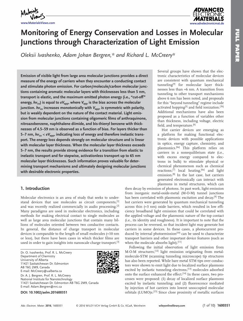
8–26 nm are shown in Figures S4 and S5 (Supporting Information). Figure 6a shows selected spectra for all four molecules, in addition to an azobenzene spectrum pre-sented previously.[3a] Since photon emission reached its maximum at different bias values for different molecules, the spectra are diffi-cult to compare for a single Vapp.
Upon initial inspection of Figure 6a, the emission spectra are qualitatively similar except for NDI which has a reproducible sec-ondary peak at ≈1.5 eV. The NDI molecule is fluorescent and exhibits a similar secondary peak at ≈1.5 eV when a single NDI molecule acts as a conductor between biased carbon nanotubes.[17] In the present case, this feature may be excited by photons from the hot car-rier photoemission at ≈2 eV. The similarity of the spectra is consistent with an emission process involving excitation of plasmons in the eC/Au contact by nonequilibrium carriers, which can then decay by emitting photons, as described above. However, the bias required to produce the spectra of Figure 6a varies significantly for different molecules, e.g, by ≈1.5 V for the case of BTB10 and NAB10. A more informative parameter for com-paring molecules is “energy loss,” defined as (eVapp − hν) and shown in Figure 6b, which
indicates directly the loss of energy between the applied bias and the emitted photons when d exceeds 5–7 nm. Figure 6c shows the spectra of Figure 6a replotted versus (eVapp − hν ) rather than hv itself, which high-lights differences in energy loss instead of hvco. Note that the spectra reverse direction on the x-axis, and clearly emphasize the observed energy loss of the highest energy emitted photon (shown by the red arrow in Figure 6c for the case of BTB10). Figure 6d shows a com-parison of the same five spectra with those of additional molecular junctions, with energy losses ranging from 0 (vertical dashed line, eVapp = hv) to 9 eV, and eVapp − hνco values from near zero for BTB7 to 7.5 eV for NAB27. The advantage of using the “loss” axis is apparent by noting that NAB10 with Vapp = −5.3 V and BTB10 with Vapp = −3.8 V have similar hvco apparent in Figure 6a equal to ≈2.8 eV. However, their spectra plotted versus (eVapp − hv) in Figure 6d are offset sig-nificantly, showing energy losses of 0.9 eV for BTB10 and 2.3 eV for NAB10 for the most energetic emitted photons. The format of Figure 6d provides a direct indication of the effect of molecular layer structure, thick-ness, and Vapp on the energy losses between the applied bias and the emitted photon, and
www.MaterialsViews.comwww.advelectronicmat.de
Adv. Electron. Mater. 2016, 1600351
Figure 4. Emission spectra from NAB10 MJs with progressively negative Vapp, plotted a) on a linear intensity scale, b) on a scale normalized to junction current, and c) on a logarithmic scale. d) Corresponding hvco for NAB10, AlOx, and NAB5.5 MJs as a function of Vapp. The “elastic” line in (d) corresponds to hvco = eVapp. Error bars in (d) were determined as described in Section S6 (Supporting Information). The dark signal from the CCD was subtracted from all spectra, and the CCD gain was ≈1 cnt per photon.
Figure 5. a) Emission spectra for a single eC/NAB8/eC MJ biased with both polarities (solid curves - negative bias, dashed curves - positive bias) on the same intensity axis. b) Intensity versus |Vapp| for the NAB8 MJ at both polarities. c) Emission spectra for Au30/eC10/NAB8/MJs with three different top contacts, as indicated, with Vapp = −4.3 V. d) Plots of hvco versus |Vapp| for two different top contacts, as indicated. Both bias polarities (red and blue lines) are shown for the eC/Au top contact.
Full p
aper
© 2016 WILEY-VCH Verlag GmbH & Co. KGaA, Weinheim (5 of 10) 1600351wileyonlinelibrary.com
permits convenient comparison of different MJs. A complete set of spectra for NAB from d = 5 to 59 nm is provided in Figure S5 (Sup-porting Information). As noted above, the emission spectrum is a complex function of the contact materials and other factors, so we rely only on the hvco for deductions about the junction electronic behavior.[3a]
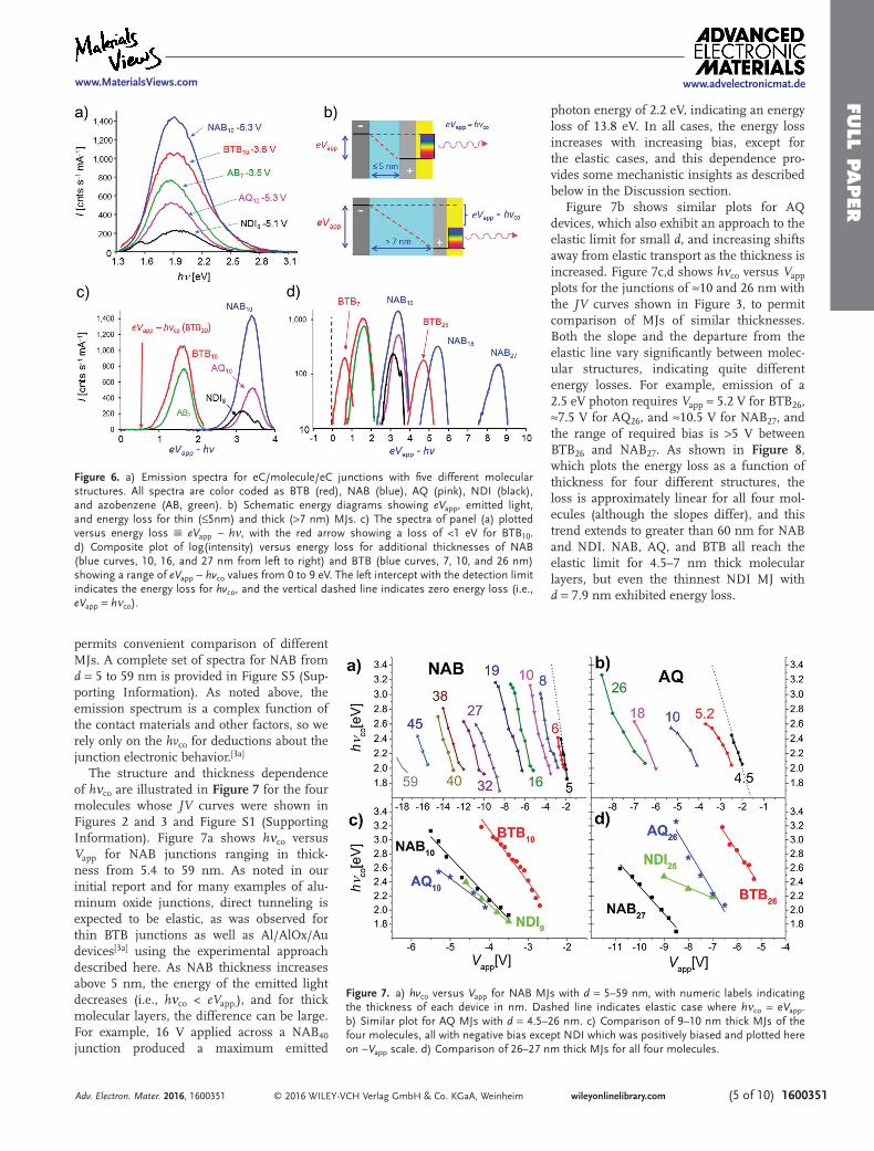
The structure and thickness dependence of hνco are illustrated in Figure 7 for the four molecules whose JV curves were shown in Figures 2 and 3 and Figure S1 (Supporting Information). Figure 7a shows hνco versus Vapp for NAB junctions ranging in thick-ness from 5.4 to 59 nm. As noted in our initial report and for many examples of alu-minum oxide junctions, direct tunneling is expected to be elastic, as was observed for thin BTB junctions as well as Al/AlOx/Au devices[3a] using the experimental approach described here. As NAB thickness increases above 5 nm, the energy of the emitted light decreases (i.e., hνco < eVapp,), and for thick molecular layers, the difference can be large. For example, 16 V applied across a NAB40 junction produced a maximum emitted
photon energy of 2.2 eV, indicating an energy loss of 13.8 eV. In all cases, the energy loss increases with increasing bias, except for the elastic cases, and this dependence pro-vides some mechanistic insights as described below in the Discussion section.
Figure 7b shows similar plots for AQ devices, which also exhibit an approach to the elastic limit for small d, and increasing shifts away from elastic transport as the thickness is increased. Figure 7c,d shows hνco versus Vapp plots for the junctions of ≈10 and 26 nm with the JV curves shown in Figure 3, to permit comparison of MJs of similar thicknesses. Both the slope and the departure from the elastic line vary significantly between molec-ular structures, indicating quite different energy losses. For example, emission of a 2.5 eV photon requires Vapp ≈ 5.2 V for BTB26, ≈7.5 V for AQ26, and ≈10.5 V for NAB27, and the range of required bias is >5 V between BTB26 and NAB27. As shown in Figure 8, which plots the energy loss as a function of thickness for four different structures, the loss is approximately linear for all four mol-ecules (although the slopes differ), and this trend extends to greater than 60 nm for NAB and NDI. NAB, AQ, and BTB all reach the elastic limit for 4.5–7 nm thick molecular layers, but even the thinnest NDI MJ with d = 7.9 nm exhibited energy loss.
www.MaterialsViews.com www.advelectronicmat.de
Adv. Electron. Mater. 2016, 1600351
Figure 6. a) Emission spectra for eC/molecule/eC junctions with five different molecular structures. All spectra are color coded as BTB (red), NAB (blue), AQ (pink), NDI (black), and azobenzene (AB, green). b) Schematic energy diagrams showing eVapp, emitted light, and energy loss for thin (≤5nm) and thick (>7 nm) MJs. c) The spectra of panel (a) plotted versus energy loss eVapp − hν, with the red arrow showing a loss of <1 eV for BTB10. d) Composite plot of log(intensity) versus energy loss for additional thicknesses of NAB (blue curves, 10, 16, and 27 nm from left to right) and BTB (blue curves, 7, 10, and 26 nm) showing a range of eVapp − hvco values from 0 to 9 eV. The left intercept with the detection limit indicates the energy loss for hvco, and the vertical dashed line indicates zero energy loss (i.e., eVapp = hνco).
Figure 7. a) hvco versus Vapp for NAB MJs with d = 5–59 nm, with numeric labels indicating the thickness of each device in nm. Dashed line indicates elastic case where hνco = eVapp. b) Similar plot for AQ MJs with d = 4.5–26 nm. c) Comparison of 9–10 nm thick MJs of the four molecules, all with negative bias except NDI which was positively biased and plotted here on −Vapp scale. d) Comparison of 26–27 nm thick MJs for all four molecules.

Full
paper
© 2016 WILEY-VCH Verlag GmbH & Co. KGaA, Weinheim1600351 (6 of 10) wileyonlinelibrary.com
The focus of the current report is on light emission from molecular junctions and the variables which affect it, rather than a detailed discussion of transport mechanisms in thick diazonium-derived molecular layers. However, a preliminary investigation of the effect temperature on NAB devices was undertaken to assist the interpretation of the light emission results. Past measurements on devices have been carried out from above room temperature to <10 K for molecular layers less than 5 nm,[4c,22] and for BTB up to 22 nm.[3b] Here, four NAB junctions were selected that both overlap and extend these previous measurements (d = 3.5, 8.0, 35, and 65 nm) over a 77–325 K temperature range. The JV behavior of the four NAB junctions at selected temperatures (all in <10−5 torr vacuum) are shown in Figure 9a.
The current density is weakly dependent on temperature for all four thickness below 200 K, with an activated response for NAB65 above 200 K. Due to the large variations in current den-sity with thickness, it was not possible to construct Arrhenius plots for the four thicknesses at a single Vapp, but Figure 9b shows ln J versus 1000/T plots at bias values with measurable current densities. Although some linear regions may be present
at high T, the plots do not exhibit classical Arrhenius behavior, with very little temperature dependence between 77 and 200 K. Table 1 lists the apparent activation energies determined from the Arrhenius slopes at low and high T, showing the lack of significant activation.
3. Discussion
Both the ubiquitous light emitting diodes and their organic equivalent OLEDs depend on recombination of electrons with holes generated by injection of charge from conducting con-tacts.[23] Light emitting tunnel junctions based on aluminum oxide generate hot carriers in the light emitting contact (usually Au, Ag, Al, or Cu) by tunneling across a thin AlOx layer.[12,24] These hot carriers then couple to plasmons in the contact which emit light. The current model for light emission by thin (d < 5 nm) organic tunnel junctions described in the Introduc-tion assumes similar hot carrier generation by coherent tun-neling, then plasmon coupling to produce light.[3a,18] The main question of the current report is how the hot carrier model changes for MJs with thickness beyond 5 nm, where coherent tunneling is unlikely. A major associated motivation is to use emitted light to probe transport mechanisms, particularly those associated with transport distances beyond the usual limits for coherent tunneling. Several experimental observations sup-port the conclusion that nonequilibrium carriers act to excite light emission from the contact(s). First, the emission spec-trum varies with contact composition, all else being constant (Figure 5c). Second, emission spectra are quite similar for dif-ferent molecules, with only NDI at high bias showing a sec-ondary peak due to luminescence. Third, the emission profile shape and high energy cut-off (hνco) are similar for both bias polarities in Au/eC/NAB/eC/Au MJs reported here, when both are viewed with the same geometry (Figure 5a,b). This result indicates that electrons traversing the MJ in either direction (toward or away from the observation point) produce qualita-tively similar light emission. However, the decreased intensity for positive bias is likely due to photon absorption by the NAB molecular layer, implying that light emission occurs more effi-ciently at the positively biased electrode. Fourth, the change in emission spectrum shape for Au and eC/Au contacts (Figure 5c) with increasing eC thickness further implies that light emis-
sion may occur from either or both of the Au and eC layers. As discussed previously, black body radiation cannot account for the emission curve shapes and positions, since the required temperatures would destroy the device.[3a] The shape of the emission spec-trum is determined largely by the properties of the contacts, while its intensity and energy loss are determined by molecular properties, namely structure and layer thickness
Although the photon emission profile is expected to vary with contact material, viewing angle, polarization, etc., the only fea-ture used in the current analysis is hvco. The device structure and observation system are capable of generating and monitoring light in
www.MaterialsViews.comwww.advelectronicmat.de
Adv. Electron. Mater. 2016, 1600351
Figure 8. Plots of eVapp − hvco at the onset of light emission for all four molecules, with their slopes indicated. Note that the x-axis intercept is similar for all cases, in the range of 4.5–6 nm. Horizontal dashed line indicates elastic transport with zero energy loss.
Figure 9. a) JV curves for negative Vapp for eC/NAB/eC MJs with the indicated thicknesses between 3.5 and 65 nm. The curves shown are overlays of a range of temperatures between 77 and 325 K. b) Arrhenius plots constructed at the indicated Vapp for all four thicknesses.

Full p
aper
© 2016 WILEY-VCH Verlag GmbH & Co. KGaA, Weinheim (7 of 10) 1600351wileyonlinelibrary.com
at least the range of 1.4–3.4 eV, so a value of hνco within that range is a direct indication of the maximum energy of the car-riers that reach the contact and stimulate light emission. This statement is supported by the similarity of hνco values for a range of bias values for both Au and eC/Au contacts, as well for both bias polarities with eC/Au (Figure 5d). Furthermore, the energy of maximum emission intensity shifts slightly with increasing Vapp, but the high energy cutoff (hvco) depends strongly on Vapp (Figure 4c). We view the plasmon mediated light emission as a “reporter” for the carrier energy reaching either contact, with the maximum emitted energy indicating the highest energy carrier traversing the junction. The general shape of the emission spectrum depends mainly on the contact material, but hνco depends directly on Vapp and energy losses in the MJ. The plasmonic properties of the light-emitting contact presumably limit the maximum photon energy, but that limit is above the 3.4 eV range apparent in Figures 4, 6, and 7. A critical point to subsequent discussion is that hνco indicates the energy after the carrier has traversed the molecular junction, since the photon can only be generated when the hot carrier reaches the contact to stimulate light emission.
As shown in Figure 7a,b, light emission from the NAB5.5 and AQ4.5 MJs satisfies the “elastic” condition, meaning that hνco = eVapp. This was also the case for the BTB7 MJ and AlOx devices reported previously,[3a] and for classical studies of Al/AlOx/Au tunnel junc-tions.[12,24,25] Therefore, the results strongly support elastic transport when d < 5 nm, with minimal change in energy loss during transport for at least an observable fraction of the carriers traversing the molecular layer. Elastic transport by coherent tunneling is one possibility, and is shown schematically in Figure 10a,b. Molecules are represented by highest occupied molecular orbital (HOMO, blue) and LUMO (red) levels between con-tacts, in which the filled levels are indicated by gray shading. The horizontal dashed line represents the electrostatic potential profile, assumed to be linear for simplicity.
Coherent tunneling is depicted in Figure 10b for negative bias of the bottom contact, resulting in a hot electron at the top electrode which then stimulates photon emission. In the elastic limit, the maximum emitted photon energy (hvco) equals eVapp, as observed experimentally for thin (d ≈ 5 nm) AQ, NAB, and BTB junctions, as well as AlOx.[3a,12,24,25] The departure of hνco from
elastic behavior observed for all junctions with d > 5 nm (or 7 nm for BTB) clearly indicates an energy loss somewhere in the system, since the maximum emitted photon energy (hνco) is significantly smaller than the input energy of eVapp. Absence of finite loss in some cases and the linearity of the loss with molecular layer thickness rules out parasitic losses in the leads or contacts, as well as significant losses during carrier injec-tion at the electrode/molecule interfaces. Figure S7 in the Sup-porting Information shows that variation of eC thickness from 2 to 25 nm in the top contact had minimal effect on either the JV response or hνco, thus ruling out significant ohmic losses inside the carbon films. Classical inelastic scattering in conductors and insulators is generally exponential with distance, whereas the losses apparent in Figure 8 are linear with thickness. Note that the slopes shown in Figure 8 (0.14–0.30 eV nm−1) are similar in magnitude to the applied electric fields assuming a linear potential profile (≈0.2–0.3 V nm−1). We conclude from the results that energy loss occurs within the molecular layer, and is associated with incoherent carrier transport, likely involving multiple steps. Figure 10c shows schematic energy levels for a 12 nm molecular layer, with the HOMO and LUMO levels shifted in accordance with the applied electric field. Note that the HOMO levels represent molecular orbitals which are separated from each other by a tunneling barrier, such as might result from nonplanar dihedral angles between molec-ular subunits. Although coherent tunneling across 12 nm is unreasonable, electrons may transfer to empty contact orbitals by either tunneling or field ionization,[3b] as shown by the red arrows. Based on the experimental results, such transport is possible for distances less than 5–7 nm, and results in a hot
www.MaterialsViews.com www.advelectronicmat.de
Adv. Electron. Mater. 2016, 1600351
Table 1. Apparent activation energies, Eact.
NAB3.5 NAB8.0 NAB35 NAB65
Vapp [V] −0.60 −1.9 −8.5 −19
Eact [meV], 225–325 K 8.9 43.5 21.0 62.3
Eact [meV], 100–200 K <1 <1 1.4 1.7
Figure 10. a) Schematic energy level diagram of a molecular junction consisting of contacts (gray), HOMO levels (blue), and LUMOs (red) in the molecular layer. Energies are referred to vacuum, with the contact Fermi level equal to −4.8 V. b) Schematic of thin molecular junction under negative bias, with dashed line indicating the electrostatic potential profile. Horizontal red arrow shows elastic transport followed by emission of light in the positive contact. c) Sche-matic for 12 nm molecular junction under negative bias, with electron transfers indicated by horizontal red arrows. d) Enlargement of molecular layer, as described in the text.

Full
paper
© 2016 WILEY-VCH Verlag GmbH & Co. KGaA, Weinheim1600351 (8 of 10) wileyonlinelibrary.com
carrier in a contact. As indicated in Figure 10c, there may be more than one HOMO which can transfer electrons to the posi-tively biased contact, resulting in photons of lower energy, but the maximum photon energy is determined by the orbital at the limit of elastic transport. As a result, hνco is less than eVapp for junctions thicker than 5–7 nm. Figure 10d shows a possible mechanism for transport within the organic layer subsequent to the initial hot electron generation. A cascade of tunneling events followed by thermal relaxation would allow electrons to traverse the film to fill the hole left behind by the hot elec-tron. These could be inelastic tunneling events[12,26] or coherent tunneling followed by vibrational relaxation, but in either case they result in an energy loss for each “step.” Furthermore, this energy loss increases with Vapp (as shown in Figure 7) if the number of “steps” stays constant. The model of Figure 10 and the experimental observations are consistent with an approxi-mately linear potential distribution in the organic layer, but not with significant potential losses as the eC/molecule interfaces.
Extensive research on transport through organic films much thicker than those examined here (generally d > 100 nm), has resulted in a collection of “hopping” models based on a sequence of discrete steps, for example, between conductive regions in a conducting polymer such as polythiophene.[27] Several of these models involve activated, Marcus-like elec-tron transfer reactions and among those is “redox exchange” in which transport occurs by a series of electron transfers in a redox or conducting polymer.[28] At least for NAB, the small activation energies of Figure 9 and Table 1 rule out Marcus-like electron transfer, since typical Eact values for reorganization exceed 200 meV. It is important to note that although the small Eact values rule out significant reorganization preceding elec-tron transport, structural changes or fluctuations after transport are still possible, with the energy dissipated in the matrix. The current results on four molecules demonstrate that inelastic, weakly activated (at least for NAB and BTB) transport can occur across distances of 6–62 nm, with an accompanying energy loss that depends on molecular structure. Research is ongoing into transport mechanisms beyond the ≈5 nm limit normally observed for elastic transport, and we anticipate that light emis-sion and associated energy losses will provide valuable evidence for elucidating transport mechanism.
4. Conclusions
Carbon based molecular junctions with molecular layer thick-nesses of 5–59 nm emit light under bias, with the spectrum and its intensity varying with molecular layer structure and thickness. Light is generated when a “hot” carrier arrives at the molecule/contact interface, then couples to surface plasmons in the contact. Junction current is symmetric with respect to bias polarity, with slightly weaker light emission for positive bias indicating that light emission occurs predominantly at the positively biased contact, with the molecular layer absorbing some of the light when the bottom contact is positive. The shape of the emission spectrum is largely determined by the properties of the contacts rather than the molecules, how-ever the maximum emitted photon energy (hvco) is limited to the applied bias, i.e., eVapp. Hence hvco indicates energy losses
during transport through the junction, with elastic transport corresponding to the case where hvco = eVapp. For AQ and NAB molecular layers, the elastic condition is satisfied for films less than 5 nm thick, and for BTB up to 7 nm. For thicker films of all molecules examined, hvco < eVapp, and the energy loss is linear with molecular layer thickness. The observed energy loss is strongly dependent on molecular structure, for example, var-ying by ≈5 eV for the four different structures and d = 26 nm (Figures 6d and 7d). The JV behavior for NAB devices is weakly dependent on temperature, with an apparent activation energy of less than 2 meV for d = 3.3–65 nm and T = 100–200 K. The results clearly indicate inelastic transport for films thicker than 5 nm, although they are not consistent with either redox exchange or classical inelastic scattering mechanisms. The near-zero Arrhenius slopes for a wide range of molecular layer thickness clearly indicate that thermally induced reorganiza-tion preceding electron transfer is unnecessary, but do not rule out energy transfer to the matrix following electron transfer. A probable transport mechanism for d > 5 nm involves mul-tiple steps down an approximately linear potential profile, with energy losses by inelastic tunneling or vibrational relaxa-tion. The ability to determine carrier energy upon arrival at the second contact/molecule interface should prove valuable for determining transport mechanism across 5–60 nm dis-tances, and ways to control transport by variation of molecular structure.
5. Experimental SectionLight emission was monitored with an Olympus BX60 microscope and fiber optic output coupled to an Andor Solis spectrograph with an Andor Newton DU-920N CCD cooled to −60 °C. Samples were mounted on a custom-built sample holder with four probes for applying an external bias using a Keithley 2602a in a DC mode. A Keithley 2602a was connected to the sample stage throughout the experiment, i.e., for initial and final i–V curve measurements as well as for DC bias application. After electrical connection, samples were aligned in the microscope stage and focused using a 50×, NA = 0.45 objective (where the field of view was approximately the same as the junction area) and an i–V curve was acquired with a Keithley 2602a to verify contact and ensure a non-shorted sample. An opaque screen was used to isolate the stage from external ambient background light. Acquisition of light consisted of the measurement of a background with no bias applied to the sample. The following spectra were measured at a constant bias (Vapp), starting at low initial bias values to verify the absence of emission at Vapp < Vonset. Acquisition was performed using four accumulations of 7.5 s with a 50 kHz readout rate, a preamplifier gain of 4×, full vertical binning, and 8 pixel horizontal binning. Intermediate measurements of i–V curves were conducted to verify sample function. Selected spectra were corrected for the spectrometer response function according the procedure described in section 5 (Supporting Information) and are shown in Figure S6 (Supporting Information) for all four junction types. The response correction had the greatest effect on the low-energy regions of the spectra, but had a minor effect (typically <0.1 eV) on the observed hvco. All hvco values reported were determined with uncorrected spectra, in part to reduce noise. Maximum photon energy, hvco values, and their uncertainties were determined by the procedure described in Section 6 and Figure S7 (Supporting Information).
Junctions were prepared as described previously,[3a] with the general structure of Au30/eC10/Molx/eC3/Au20. Details regarding molecular layer and contact deposition specific to the current report are provided in section 8 (Supporting Information). J–V curve measurements and DC
www.MaterialsViews.comwww.advelectronicmat.de
Adv. Electron. Mater. 2016, 1600351

Full p
aper
© 2016 WILEY-VCH Verlag GmbH & Co. KGaA, Weinheim (9 of 10) 1600351wileyonlinelibrary.com
www.MaterialsViews.com www.advelectronicmat.de
Adv. Electron. Mater. 2016, 1600351
bias application were performed using a Keithley 2602a SourceMeter in a four probe configuration[29] to minimize contact resistance errors. JV curves were collected starting from 0 V, sweeping toward positive or negative direction to reach limiting current density of ca. ±30 A cm−2. Notably, most of the junctions were able to tolerate higher current densities, up to 100 A cm−2 using fast scans, but JV curves measured with the limiting current of ±30 A cm−2 provided sufficient information and intact junctions for further light emission measurements. 100 data points, with NPLC 0.001, and filter 10 were used for each polarity measurement, with a nominal duration 0.1 s to avoid junction breakdown. Temperature dependent measurements were performed similarly using Keithley 2602a, connected to a Janus ST-500-1-4CX vacuum probe station with liquid nitrogen cooling. Base pressure during data accumulation was 1–2 × 10⁻⁶ mbar. Measurement started at 77 K followed by slow heating up to room temperature, using a Scientific Instruments 9700 temperature controller. At each temperature, the sample was allowed to stabilize for ca. 5 min before JV curves were recorded.
JV curves obtained before and after light emission had similar shapes. A single light emission measurement at a lower bias, close to the onset of light emission, did not affect the current density of the junction. Extensive measurement at increased biases (>2 V higher than onset voltage) for 3–5 min caused a decrease in current density by 50%–90%. If significant DC bias caused junction breakdown due to short circuit, light emission terminated, confirming that light generation could not proceed in the presence of direct short between the contacts.
Supporting InformationSupporting Information is available from the Wiley Online Library or from the author.
AcknowledgementsThis work was supported by the University of Alberta, the National Research Council of Canada, the National Science and Engineering Research Council, and the Alberta Innovates Technology Futures. The authors thank Amin Morteza Najarian, Mykola Kondratenko, Akhtar Bayat, and Jerry Alfred Fereiro for the synthesis of diazonium salts used for fabrication of MJs and Prof. Jean-Christophe Lacroix of the University of Paris for providing the BTB amine precursor used to prepare BTB molecular junctions.
Received: August 31, 2016Published online:
[1] a) R. M. Metzger, Chem. Rev. 2015, 115, 5056; b) N. Amdursky, D. Marchak, L. Sepunaru, I. Pecht, M. Sheves, D. Cahen, Adv. Mater. 2014, 26, 7142; c) R. L. McCreery, A. J. Bergren, Adv. Mater. 2009, 21, 4303; d) A. Vilan, O. Yaffe, A. Biller, A. Salomon, A. Kahn, D. Cahen, Adv. Mater. 2010, 22, 140; e) A. Salomon, D. Cahen, S. Lindsay, J. Tomfohr, V. B. Engelkes, C. D. Frisbie, Adv. Mater. 2003, 15, 1881; f) J. R. Heath, Annu. Rev. Mater. Res. 2009, 39, 1; g) P. Song, C. S. S. Sangeeth, D. Thompson, W. Du, K. P. Loh, C. A. Nijhuis, Adv. Mater. 2016, 28, 631; h) A. Wan, C. S. Suchand Sangeeth, L. Wang, L. Yuan, L. Jiang, C. A. Nijhuis, Nanoscale 2015, 7, 19547.
[2] A. J. Bergren, L. Zeer-Wanklyn, M. Semple, N. Pekas, B. Szeto, R. L. McCreery, J. Phys.: Condens. Matter 2016, 28, 094011.
[3] a) O. Ivashenko, A. J. Bergren, R. L. McCreery, J. Am. Chem. Soc. 2016, 138, 722; b) H. Yan, A. J. Bergren, R. McCreery,
M. L. Della Rocca, P. Martin, P. Lafarge, J. C. Lacroix, Proc. Natl. Acad. Sci. USA 2013, 110, 5326.
[4] a) S. H. Choi, B. Kim, C. D. Frisbie, Science 2008, 320, 1482; b) H. B. Akkerman, R. C. G. Naber, B. Jongbloed, P. A. van Hal, P. W. M. Blom, D. M. de Leeuw, B. de Boer, Proc. Natl. Acad. Sci. USA 2007, 104, 11161; c) A. J. Bergren, R. L. McCreery, S. R. Stoyanov, S. Gusarov, A. Kovalenko, J. Phys. Chem. C 2010, 114, 15806; d) V. B. Engelkes, J. M. Beebe, C. D. Frisbie, J. Am. Chem. Soc. 2004, 126, 14287; e) R. Har-Lavan, O. Yaffe, P. Joshi, R. Kazaz, H. Cohen, D. Cahen, AIP Adv. 2012, 2, 012164.
[5] S. H. Choi, C. Risko, M. C. R. Delgado, B. Kim, J.-L. Bredas, C. D. Frisbie, J. Am. Chem. Soc. 2010, 132, 4358.
[6] a) M. L. Brongersma, N. J. Halas, P. Nordlander, Nat. Nanotechnol. 2015, 10, 25; b) S. A. DiBenedetto, A. Facchetti, M. A. Ratner, T. J. Marks, J. Am. Chem. Soc. 2009, 131, 7158.
[7] S. Mukherjee, L. Zhou, A. M. Goodman, N. Large, C. Ayala-Orozco, Y. Zhang, P. Nordlander, N. J. Halas, J. Am. Chem. Soc. 2014, 136, 64.
[8] K. Turvey, J. W. Allen, J. Phys. C: Solid State Phys. 1973, 6, 2887.[9] a) P. D. Sparks, J. E. Rutledge, Phys. Rev. B 1989, 40, 7574;
b) A. M. Goodman, Phys. Rev. 1966, 144, 588; c) A. M. Goodman, J. Appl. Phys. 1970, 41, 2176.
[10] V. V. Afanas’ev, Internal Photoemission Spectroscopy: Principles and Applications, Elsevier Science, Oxford, UK 2008.
[11] a) J. A. Fereiro, M. Kondratenko, A. J. Bergren, R. L. McCreery, J. Am. Chem. Soc. 2015, 137, 1296; b) J. A. Fereiro, R. L. McCreery, A. J. Bergren, J. Am. Chem. Soc. 2013, 135, 9584.
[12] J. Lambe, S. L. McCarthy, Phys. Rev. Lett. 1976, 37, 923.[13] A. Yu, S. Li, G. Czap, W. Ho, Nano Lett. 2016, 16, 5433.[14] a) E. Flaxer, O. Sneh, O. Cheshnovsky, Science 1993, 262, 2012;
b) D. Fujita, T. Ohgi, W. L. Deng, K. Ishige, T. Okamoto, S. Yokoyama, T. Kamikado, S. Mashiko, Surf. Sci. 2001, 493, 702; c) G. Hoffmann, L. Libioulle, R. Berndt, Phys. Rev. B 2002, 65, 212107
[15] a) Z. C. Dong, X. L. Guo, A. S. Trifonov, P. S. Dorozhkin, K. Miki, K. Kimura, S. Yokoyama, S. Mashiko, Phys. Rev. Lett. 2004, 92, 086801; b) F. Rossel, M. Pivetta, W. D. Schneider, Surf. Sci. Rep. 2010, 65, 129.
[16] T. Shamai, Y. Selzer, Chem. Soc. Rev. 2011, 40, 2293.[17] C. W. Marquardt, S. Grunder, A. Błaszczyk, S. Dehm, F. Hennrich,
H. V. Löhneysen, M. Mayor, R. Krupke, Nat. Nanotechnol. 2010, 5, 863.
[18] W. Du, T. Wang, H.-S. Chu, L. Wu, R. Liu, S. Sun, W. K. Phua, L. Wang, N. Tomczak, C. A. Nijhuis, Nat. Photonics 2016, 10, 274.
[19] a) S. Y. Sayed, A. Bayat, M. Kondratenko, Y. Leroux, P. Hapiot, R. L. McCreery, J. Am. Chem. Soc. 2013, 135, 12972; b) R. McCreery, H. Yan, A. J. Bergren, Phys. Chem. Chem. Phys. 2013, 15, 1065; c) S. Y. Sayed, J. A. Fereiro, H. Yan, R. L. McCreery, A. J. Bergren, Proc. Natl. Acad. Sci. USA 2012, 109, 11498.
[20] H. Yan, A. J. Bergren, R. L. McCreery, J. Am. Chem. Soc. 2011, 133, 19168.
[21] a) A. J. L. Ferguson, P. Dawson, D. G. Walmsley, J. Phys.: Condens. Matter 1989, 1, 9021; b) P. Dawson, D. G. Walmsley, H. A. Quinn, A. J. L. Ferguson, Phys. Rev. B 1984, 30, 3164.
[22] A. M. Mahmoud, A. J. Bergren, N. Pekas, R. L. McCreery, Adv. Funct. Mater. 2011, 21, 2273.
[23] a) T. Sengoku, T. Yamao, S. Hotta, J. Non-Cryst. Solids 2012, 358, 2525; b) C. Fan, C. Yang, Chem. Soc. Rev. 2014, 43, 6439; c) J.-H. Jou, S. Kumar, A. Agrawal, T.-H. Li, S. Sahoo, J. Mater. Chem. C 2015, 3, 2974; d) X. Yang, G. Zhou, W.-Y. Wong, Chem. Soc. Rev. 2015, 44, 8484.
[24] a) S. L. McCarthy, J. Lambe, Appl. Phys. Lett. 1978, 33, 858; b) J. R. Kirtley, T. N. Theis, J. C. Tsang, Appl. Phys. Lett. 1980, 37,

Full
paper
© 2016 WILEY-VCH Verlag GmbH & Co. KGaA, Weinheim1600351 (10 of 10) wileyonlinelibrary.com
www.MaterialsViews.comwww.advelectronicmat.de
Adv. Electron. Mater. 2016, 1600351
436; c) J. Kirtley, T. N. Theis, J. C. Tsang, Phys. Rev. B 1981, 24, 5650.
[25] T. N. Theis, J. R. Kirtley, D. J. DiMaria, D. W. Dong, Phys. Rev. Lett. 1983, 50, 750.
[26] R. Berndt, J. K. Gimzewski, P. Johansson, Phys. Rev. Lett. 1991, 67, 3796.
[27] a) J. C. Lacroix, K. I. Chane-Ching, F. Maquere, F. Maurel, J. Am. Chem. Soc. 2006, 128, 7264; b) E. Johansson, S. Larsson, Synth.
Met. 2004, 144, 183; c) A. S. Dhoot, G. M. Wang, D. Moses, A. J. Heeger, Phys. Rev. Lett. 2006, 96, 246403.
[28] a) R. H. Terrill, R. W. Murray, in Molecular Electronics (Eds: J. Jortner, M. Ratner), Blackwell Science Ltd., Cambridge, MA, 1997, p. 215; b) S. Ranganathan, R. W. Murray, J. Phys. Chem. B 2004, 108, 19982; c) D. A. Buttry, F. C. Anson, J. Am. Chem. Soc. 1983, 105, 685.
[29] A. J. Bergren, R. L. McCreery, Annu. Rev. Anal. Chem. 2011, 4, 173.