monopolar biphasic stimulator with discharge function and
TRANSCRIPT

568 IEEE TRANSACTIONS ON BIOMEDICAL CIRCUITS AND SYSTEMS, VOL. 15, NO. 3, JUNE 2021
Monopolar Biphasic Stimulator With DischargeFunction and Negative Level Shifter for
Neuromodulation SoC Integration in Low-VoltageCMOS Process
Chia-Chi Hsieh and Ming-Dou Ker , Fellow, IEEE
Abstract—A 16-channel monopolar biphasic stimulator chipwith discharge function for biomedical applications is proposed anddesigned. To provide monopolar biphasic stimulus currents, thepositive (6V) and the negative (-6V) voltage sources are supportedto generate the desired current pulses of ±3 mA. The monopolarbiphasic stimulator chip was fabricated in a 0.18-µm 1.8-V/3.3-VCMOS process with the common grounded p-type substrate. Theoverstress and reliability issues on the low-voltage transistors inthe stimulator circuits were fully overcome by circuit design. Thesilicon area of each single channel only occupies 0.08 mm2 and theoutput level of stimulus current is up to ±3 mA. By applying thedischarge function, safety concern of unbalanced charge in neuro-stimulation can be dealt properly. The residual average dc currentis less than 3.42 nA after discharge is activated. Moreover, this chiphas also been verified with both in-vitro imitation measurementand in-vivo animal test.
Index Terms—Biphasic stimulus, charge balance, monopolarstimulator, neuro-modulation, deep brain stimulation.
I. INTRODUCTION
N EUROLOGICAL disorder such as Parkinson’s disease orepilepsy afflicts about 1% of the world’s population. Com-
bining with medical treatment, functional electrical stimulation(FES) has recently been developed and widely used in neuro-modulation to achieve better therapeutic efficacy. Therefore, thestimulator system often integrates with other helpful devices toadapt various biomedical applications from old days to moderndays [1]–[3]. For instance, Fig. 1 shows an implanted system onchip (SoC), which is placed in implantable impulse generator(IPG) case, incorporates with external control that consists of
Manuscript received February 17, 2021; revised April 21, 2021 and May24, 2021; accepted June 2, 2021. Date of publication June 7, 2021; date ofcurrent version August 17, 2021. This work was supported in part by the “Centerfor Neuromodulation Medical Electronics Systems” from The Featured AreasResearch Center Program within the framework of the Higher Education SproutProject by the Ministry of Education (MOE) in Taiwan and in part by theMinistry of Science and Technology (MOST), Taiwan, under Contracts MOST110-2321-B-009-004 and MOST 109-2221-E-009-100-MY3. (Correspondingauthor: Ming-Dou Ker.)
The authors are with the Biomedical Electronics Translational ResearchCenter, National Yang Ming Chiao Tung University, Hsinchu 300, Taiwan(e-mail: [email protected]; [email protected]).
Color versions of one or more figures in this article are available at https://doi.org/10.1109/TBCAS.2021.3087036.
Digital Object Identifier 10.1109/TBCAS.2021.3087036
Fig. 1. Block diagram of the closed-loop implantable SoC for Parkinson’sdisease with its equivalent electrode-tissue model.
a graphic user interface (GUI) and a bilateral data transceiverto realize a closed-loop network. The implanted SoC is com-prised of a power management unit (PMU), bio-signal processer(BSP), neural-signal acquisition (NSA), voltage generator, andstimulator. PMU provides the powers to other circuit blocks,and recharges itself wirelessly through coils from the outsideof the human body. The monopolar stimulator is powered bythe voltage generator which is able to generate positive andnegative high voltages from lower voltages provided by thePMU. Due to the perspective of on-chip integration and energyefficiency, charge pumps are often adopted for stimulators inmicroelectronic implantation [4]–[8]. BSP serves as a commu-nication interface between the external control and the implantedSoC. The BSP guarantees that all the biological data receivedfrom the NSA will be monitored on the GUI, and gives propercommands to the stimulator in order to generate FES towardpatients. Stimulation pulses are then delivered to electrode leadsthrough SoC outputs (E1 to E16), which are shared by theNSA and stimulator. In deep brain stimulation (DBS) therapyfor Parkinson’s disease, electrode leads are formed as a finecylinder with conductive segments [9]. As for epileptic seizurecontrol, intracranial electrodes are used for regional stimulation[10]. The electrode array of multi-pixel architecture is designedfor sub-retinal prosthetic [11]. According to different biomed-ical applications, diverse electrode types are devised to benefit
1932-4545 © 2021 IEEE. Personal use is permitted, but republication/redistribution requires IEEE permission.See https://www.ieee.org/publications/rights/index.html for more information.
Authorized licensed use limited to: IEEE Associate Editors. Downloaded on August 14,2021 at 14:21:34 UTC from IEEE Xplore. Restrictions apply.

HSIEH AND KER: MONOPOLAR BIPHASIC STIMULATOR WITH DISCHARGE FUNCTION AND NEGATIVE LEVEL 569
the treatment effect. Furthermore, stimulus configurations canbe divided into monopolar (unipolar) and bipolar (H-bridge).Some studies showed that the monopolar configuration hasmore advantages in specific field, as compared to that of thebipolar structure [12]–[15]. In this work, the monopolar biphasicstimulator is developed for DBS applications.
Depending on distinct electrode area, material, and the loca-tion of implantation, the output impedance of stimulator maychange from case to case. Ordinarily, a simplified model of theelectrode-tissue impedance includes a double-layer capacitance(CDL), a charge-transfer resistance (RCT), and a spread resis-tance (RS) [16], [17]. The resistance scale of RCT is usuallyreported high value from hundreds of kilo-ohm to mega-ohm,hence considered as open circuit to the stimulus current [17]–[19]. Therefore, the minimum positive high voltage from thevoltage generator can be calculated as
VCCMIN = IMAX_A × RS + (IMAX_A × TANO)/CDL
+VH_MIN, (1)
where IMAX_A, TANO, and VH_MIN are the maximum anodicstimulus current, anodic stimulus time, and minimum voltageheadroom for the current generator circuit, respectively. Dueto the symmetrical characteristic of the monopolar stimulator,the specification of minimum negative high voltage can beobtained from a similar calculation with minus sign. Mostly,the range of CDL is from hundred nano-farad to micro-farad,except for tiny size of electrodes used in retinal prosthesis areunder 50 nF. Regarding of the value of RS, it is often less than10 kΩ [11], [17]–[19]. It can be calculated from (1) that thevoltage difference on RS is the main factor which determinesVCCMIN of the stimulator circuit, compared to the voltageaccumulated on CDL during stimulation phase. Thus, accordingto the wide range of RS, stimulus drivers are designed to toleratethe voltage compliance, and circuit schemes such as adaptivegate bias or CMOS stack techniques have been proposed toavoid the gate-oxide overstress of the transistors [20], [21]. Inaddition, in monopolar configuration, the drivers need to standeven higher voltage difference than bipolar structure. It can bederived from (1) that during the anodic stimulation phase, thevoltage difference of half of the stimulator drivers are calculatedas
VDIFF_M = (IMAX_A × RS + (IMAX_A × TANO)/CDL)
− (−VCCMIN). (2)
That is to say, the driver of monopolar stimulator has totolerate the voltage of 2VCCMIN – VH_MIN during stimulationphase.
This paper is organized as follows. Section II presents a briefdiscussion of stimulus configurations. In Section III, the circuitdesign and implementation details of the proposed monopolarstimulator will be presented. Section IV demonstrates the ex-perimental results that include electrical verifications, in-vitroimitation measurements, and in-vivo animal test. Finally, theconclusion is given in Section V.
II. DISCUSSION OF STIMULUS CONFIGURATIONS
Figs. 2(a) and (b) present the conceptual circuit structureof monopolar and bipolar stimulus configurations those areused in neuro-stimulation. Both are reported effective for neuraldisorders as mentioned in previous section. However, regard-less of which circuit structure is demanded, biphasic stimuli(ISTI) shown in Fig. 2(c) is needed for minimizing redundantcharges in the body to avoid physiological harm [20]–[23]. Themost obvious difference between monopolar and bipolar is thatthe former completes biphasic stimulation through the currentsource from the positive high voltage (+VCC) and the currentsink from ground to the negative high voltage (–VCC) by driverswitches in a single stimulus driver. As illustrated in Fig. 2(a),switches SM1, SM2 and SM3 are built for anodic stimulation,cathodic stimulation, and discharge, respectively. On the otherhand, biphasic pulses can be generated by bipolar circuit withonly the positive high voltage (+VCC). Fig. 2(b) indicates themethod of anodic stimuli that the stimulus current sequentiallyflows through SB1, tissue, and SB4. In contrast, SB2 and SB3
compose the cathodic stimuli current path. SB2 and SB4 arefor discharge operation. Another circuit structure of bipolarstimulator includes both the current source and the current sink[24], [25]. Nevertheless, driver switches in two different stimulusdrivers are chosen to achieve the bi-directional current deliv-ering. Therefore, in order to generate a single biphasic pulse,bipolar structure doubles the silicon area on driver circuits. Inthe bipolar structure, all the devices are operated under positivevoltage whether in anodic, cathodic, or discharge phase. On thecontrary, monopolar configuration requires both positive andnegative voltages to accomplish the biphasic stimulation. Thedevices those operate with negative voltage should be carefullydeal with all the parasitic junction diodes, because the voltageof p-substrate has to be tied to 0 V instead of the most negativevoltage for SoC integration with other circuit blocks together. Inthe closed-loop implantable SoC system, not only analog blocksbut also digital circuits are included. The digital circuits areusually implemented through automatic placement and routing(APR) flow to generate the circuit layout with the standardcells provided from foundry, in which the p-substrate has beendirectly tied to 0 V. Therefore, the common p-substrate of a SoC,including stimulator circuit, analog frond-end blocks, and digitalcircuit blocks, has to be tied to 0 V for all circuit blocks in thelow-voltage CMOS technology.
As shown in Fig. 3(a), when the PMOS operates in a negativecondition and the p-sub is biased at 0 V, the current can easilyflow through p-sub/n-well diode (PD2) and causes side effectson the circuit behavior. Fig. 3(b) shows the cross-sectional viewof a deep n-well NMOS. Under the situation of negative voltageoperation, the deep n-well is indispensable to isolate p-well fromp-sub, and is usually biased to the highest voltage in the circuitto prevent current leakage from parasitic diodes ND2 and ND3.Since the bulk and source terminals are generally bound togetherin analog design to avoid body effect, the n+/p-well diode (ND1)in NMOS will not suffer from junction leakage. Therefore, aslong as the voltage differences between p-well/deep n-well anddeep n-well/p-sub are within process limitation, NMOS can
Authorized licensed use limited to: IEEE Associate Editors. Downloaded on August 14,2021 at 14:21:34 UTC from IEEE Xplore. Restrictions apply.

570 IEEE TRANSACTIONS ON BIOMEDICAL CIRCUITS AND SYSTEMS, VOL. 15, NO. 3, JUNE 2021
Fig. 2. Conceptual circuit structure of (a) monopolar and (b) bipolar stimulus configurations. The operation of cathodic/anodic stimulation and discharge withelectrode-tissue model are labeled, respectively. (c) The control sequence of the output current (ISTI) for the biphasic stimulus with cathodic (CAT), anodic (ANO),and discharge (DIS) phases.
Fig. 3. Cross-sectional view and corresponding parasitic diode paths of (a)PMOS and (b) NMOS with deep n-well.
be realized in negative voltage with all the parasitic junctiondiodes are reverse biased. As a result, NMOS is more reliablethan PMOS in LV CMOS process regarding negative voltageimplementation [4], [6]. As for the voltage level of output nodes,ST_OUT1 and ST_OUT2 in Fig. 2(b) are always in the positivevoltage domain. However, ST_OUT in Fig. 2(a) will changefrom the negative to positive voltage during biphasic stimulation.At the meantime, discharge path should remain off state when thestimulus current is delivered. Since the discharge path is builtbetween ST_OUT and ground for shorting operation, devicesthat are used in discharge circuit have to fit the various powerdomain. Thus, the terminal voltage of every PMOS and NMOSthat are jointed to ST_OUT should be cautious of the p+/n-welldiode (PD1) and n+/p-well (ND1) diode leakage.
III. PROPOSED MONOPOLAR STIMULATOR CIRCUIT
The block diagram of proposed monopolar biphasic stimula-tor (one-lead, 8-channel) is shown in Fig. 4, which is composedof a digital control decoder, a reference current source (RCS),a 4-bit current digital-to-analog converter (DAC), a biphasiccurrent generator (BCG), and 8-channel stimulus drivers. Thedigital input signals will first be processed through the decoder,which then gives the order to the drivers for channel selection andstimulus sequence. As for the stimulus current level, it is decidedby 4-bit binary code AMP[3:0]. Initially, a reference current(IREF) is generated by RCS, which preserves the trimmingprobability (TRIM[2:0]) against process variation. Next, IREF
is mirrored and multiplied by the corresponding MOS size in thecurrent DAC to provide 15 current steps of IDAC. Finally, the
Fig. 4. The block diagram of proposed monopolar biphasic stimulator (drawnwith one lead).
BCG divides IDAC into two current paths, and enlarges IDAC tothe desired stimulus current level. At last, the biphasic currentwill be delivered by the chosen channel (driver). In the proposedstimulator, all the drivers share the same RCS, current DAC andthe BCG. The stimulator is designed for SoC integration, so thelow operating voltages of 1.8 V (VDDL) and 3 V (VDDH) aregenerated from the PMU. Other powers including the positivehigh voltage of 6 V (2VDDH), the negative low voltage of –3 V(–VDDH), and the negative high voltage of –6 V (–2VDDH) canbe provided by the on-chip charge pump circuits. Those werenot included into this paper presentation with main focus on thestimulator circuit design. All the digital control inputs are 0 Vto 1.8 V.
A. Stimulus Driver
Fig. 5 shows the transistor-level of a single driver with BCGand the power domain of all related control circuits. Stimulusdrivers are designed to tolerate the voltage compliance from2VDDH to –2VDDH, i.e. 12-V voltage difference, and each drivercomprises driver switches (MPD1 and MND1), stack transistors(MPD2, MPD3, MND2, and MND3), the discharge circuit, dis-charge and sensing control, and the corresponding level shifters.The current sink and current source are generated by the BCGcircuit for cathodic and anodic stimulus. Despite driver switchesare contained in the stimulus driver, current switches are alsoused in the BCG not only to disable the current sink and currentsource but also to prevent any of the leakage paths. Therefore,the digital control signals are shifted from 0 V to –VDDH and
Authorized licensed use limited to: IEEE Associate Editors. Downloaded on August 14,2021 at 14:21:34 UTC from IEEE Xplore. Restrictions apply.

HSIEH AND KER: MONOPOLAR BIPHASIC STIMULATOR WITH DISCHARGE FUNCTION AND NEGATIVE LEVEL 571
Fig. 5. Transistor-level schematic of a single driver (channel) with biphasiccurrent generator and the power domain of related control circuits.
VDDL to 0 V by the negative low-side level shifter (N-LSLS) forblocking the stimulus current in the current DAC before IDAC isamplified. Meanwhile, the positive and negative high-side levelshifter (P-HSLS and N-HSLS) turns off the current source orcurrent sink by transferring the control logic state from VDDL
to 2VDDH or –2VDDH. The logic low and logic high states ofP-HSLS (N-HSLS) are VDDH (–2VDDH) and 2VDDH (–VDDH).Since the voltage difference between all the logic states is within3 V, overstress issues can be successfully avoided.
As aforementioned in Fig. 2(c), the control sequence ofbiphasic output waveform in one stimulation period includescathodic (CAT), anodic (ANO), discharge (DIS), and a shortinter-phase delay between the control signals. In Fig. 5, all thedriver switches stay off at the beginning. SDA and SDC arethe control signals of stimulus driver that shifted by P-HSLSand N-HSLS respectively. When a specified channel is selectedfor cathodic stimulation, SDC is transferred from logic low(–2VDDH) to logic high (–VDDH), yet MPD1 remains off. Thecathodic stimulus current (ICAT) then sinks from the ground ofbio-tissue through ST_OUT (electrode) to –2VDDH via MND3,MND2, and MND1. The anodic stimulus current (IANO) is deliv-ered in a similar way, MND1 is turned off and the logic state ofSDA changed from high (2VDDH) to low (VDDH), which allowsIANO to flow to the bio-tissue through MPD1, MPD2, and MPD3.Thus, the biphasic current stimulus pattern can be generated bythe monopolar stimulator.
With the maximum output voltage of ±3 V in this work,VDIFF_M in equation (2) of stimulus driver reaches 9 V underthe supply voltages of ±6 V. To prevent device overstress, thestack transistors MPD2 and MND2 are biased at VDDH and–VDDH separately, and both MPD3 and MND3 are biased at 0 V.Regardless of either the ICAT or IANO is delivered, which leadsthe drain voltage of MPD3 and MND3 to negative or positive, withsuitable n-well/p-well bias of 3.3-V devices, the driver can avoidp-n junction forward leakage when the p-substrate is 0 V. Among
Fig. 6. Transistor-level schematic of the biphasic current generator circuit.
all the stimulus drivers, one channel will be enabled during astimulation period. For those channels that are not selected, SDC
is at logic low and SDA is at logic high, which represents that twodriver switches are off, and the driver circuit is in high-Z state.Under high-Z circumstance, even if the disabled drivers sensethe artifacts on ST_OUT caused by the enabled neighborhoodchannel, driver devices still do not suffer from overstress issuedue to MPD2, MPD3, MND2, and MND3.
Discharge circuit is driven by the discharge and sensingcontrol. In discharge phase, the redundant charge on bio-tissueresult from the mismatch between ICAT and IANO will be resetby shorting ST_OUT to the ground through discharge circuit.The BCG is off during discharge operation, as well as MPD1
and MND1. After electrodes are discharged, the NSA recordsbio-signals with the built in preamplifiers. The electrode nodesare shared by the stimulator and NSA, which is also realizedin LV CMOS process. A conductive path is provide in thestimulator for NSA so that the negative and positive voltageson electrodes caused by ISTI and RS can be blocked during thestimulus phase. Thus, the discharge circuit prevents the circuitin NSA from device overstress and junction leakage problem.
B. Biphasic Current Generator (BCG)
Fig. 6 shows the transistor-level schematic of BCG circuit,which is composed of the 4-bit current DAC and three currentpaths. The first current path contains MP1 to MP3 and MN1 toMN5. The second current path consists of MP4, MP5, and MN6 toMN11. Regarding to the third current path, the node A and nodeC serve as the current source (IANO) and the current sink (ICAT)for the stimulus drivers. All the current switches (MP1, MN8,MASW1, MCSW1, and MCSW2) are controlled by the digital inputsignals CAT or ANO to turn on or off in the stimulus phase. Sincethe 4-bit current DAC is shared by IANO and ICAT, IDAC flowsfrom VDDL to –2VDDH in the first current path after generatedfrom the current DAC, and then mirrored to the second current
Authorized licensed use limited to: IEEE Associate Editors. Downloaded on August 14,2021 at 14:21:34 UTC from IEEE Xplore. Restrictions apply.

572 IEEE TRANSACTIONS ON BIOMEDICAL CIRCUITS AND SYSTEMS, VOL. 15, NO. 3, JUNE 2021
Fig. 7. Level shifters served as logic control circuit in the proposed stimulator. (a) Positive high-side level shifter (P-HSLS) with voltage limiting technique. (b)Voltage limiting technique with PMOS and NMOS causes reliability issue in the negative high-side level shifter (N-HSLS). (c) Proposed N-HSLS that can dealwith the reliability issue of MOSFETs realized in the negative power domain.
path. So, the current source can be powered by 2VDDH to getthe sufficient headroom for IANO delivering. Finally, IANO andICAT will be amplified 40 times in the third current path by MP6,MP7, MN12, and MN13. Due to the transferring from VDDL to2VDDH in the positive power domain, the devices drawn withthick gate in Fig. 6 are 3.3-V devices. MP1 and the transistorsthose are used in the 4-bit current DAC are 1.8-V devices.
However, the voltage differences across the current paths arehigher than the normal operation voltage of LV devices. In orderto guarantee that all the current paths are free from overstressissue, stack transistors (MP2, MP3, MN6, MN7, and MN9) withproper gate bias voltages and diode-connected MOSFETs (MN1,MN2, and MN3) are added in the BCG. The bulk terminal ofMP3 is tied to 0 V instead of its source terminal to prevent theforward bias of p-sub/n-well junction since MP3 operates inthe negative power domain. As for the current switches, MN8,MASW1, MCSW1, and MCSW2, the logic levels of gate controlsignals are shifted from 0 V to VDDL to a proper logic states byN-LSLS, P-HSLS, N-HSLS, and N-HSLS, respectively. SBCG
is the gate control signal of MP1, its logic state remains 0 Vduring the stimulation phase. Otherwise, SBCG keeps at VDDL
to turn off MP1 in order to block IDAC. MN8 only turns onduring the anodic phase with gate control of 0 V. MASW1 isused to disable IANO. When MASW1 is on, the gate bias of MP4
and MP6 will be pulled up to 2VDDH, thus to stop the currentmirrored path. MCSW1 and MCSW2 are corresponding to ICAT,and they operate in the opposite situation. To generate ICAT,MCSW1 is on and MCSW2 is off, which complete the currentmirrored path. When ICAT has to be disabled, MCSW1 is offand MCSW2 is on. MN13 will be off since the gate bias is pulledlow to –2VDDH by MCSW2. At the meantime, MCSW1 is off toprevent –2VDDH from passing to the first and the second currentpaths.
In summary, during the cathodic phase, MP1, MASW1, andMCSW1 are on, while MN8 and MCSW2 are off. During theanodic phase, MP1, MN8, MCSW2 are on, while MASW1 andMCSW1 are off. In non-stimulation phase, MASW1 and MCSW2
TABLE ITHE RATIO OF MOSFETS USED IN P-HSLS AND N-HSLS
are on, while MP1, MN8, and MCSW1 are off. Thus, the currentswitches not only disable the current sink and current source butalso prevent any of the leakage paths in the BCG circuit.
C. Level Shifter in Negative Voltage
The circuit scheme of the high-side level shifters that areused in the proposed stimulator with 3.3-V devices are shown inFig. 7. The corresponding ratio of MOSFETs used in P-HSLSand N-HSLS are listed in Table I. In the P-HSLS (Fig. 7(a)), thelogic state of digital control Vin from 0 V to VDDL can be shiftedto VDDH to 2VDDH. Voltage limiting technique with NMOS(MN1 and MN2) and PMOS (MP3 and MP4) is implemented toavoid terminal overstress of MOSFETs [26]. The output voltagelevel is latched by cross-coupled pair MP1 and MP2 as conven-tional level shifters. However, for the N-HSLS in Fig. 7(b), thepower domain covers from VDDL to –2VDDH. Even though thevoltage limiting transistors MN1, MP3, MN2, and MP4 operatein a normal voltage range, the voltage limiting technique stillfails because of the p-sub/n-well forward bias of PMOS (MP5
and MP6) that are immersed in negative voltage. At the push-pullbuffer stage, MP7 also encounters the same issue. In [6] and [27],the negative level shifters are designed with HV transistors. The
Authorized licensed use limited to: IEEE Associate Editors. Downloaded on August 14,2021 at 14:21:34 UTC from IEEE Xplore. Restrictions apply.

HSIEH AND KER: MONOPOLAR BIPHASIC STIMULATOR WITH DISCHARGE FUNCTION AND NEGATIVE LEVEL 573
Fig. 8. Cross-sectional view of stack body diode connected transistors MN1
to MN6 (MN7 to MN12) used in proposed N-HSLS.
isolated rings in HV process such as deep p-well and n+ buriedlayer keep off the negative voltage from transistors. In [28],another structure of negative level shifter is implemented under0.18-µm triple-well standard CMOS technology, however, thevoltage level of logic low only reaches to –3.3 V.
Fig. 7(c) illustrates the proposed N-HSLS that transfers thelogic low of digital control signals from 0 V to –2VDDH andlogic high from VDDL to –VDDH. Voltage limiting transistorsare replaced by stack devices (MN1 to MN6 and MN7 to MN12)between 0 V and –VDDH. The gate terminal of each NMOSis connected to its source, and the bulk terminal is jointed toits drain. In this case, the current is forced to flow through theparasitic p-n junction diode instead of the channel of MOSFETs.The cross-sectional view of stack devices is shown in Fig. 8.Since the deep n-well is tied to VDDL, which is the highestvoltage level of the N-HSLS, the parasitic BJT stays in offstate. Hence, redundant leakage current can be avoided in thestack devices. Owing to the higher cut-in voltage of the p-njunction compared to the turn-on voltage of the MOS channel,the voltage drop of the body diode connection scheme is largerthan diode-connected MOS [29]. Therefore, the body diodeconnection reduces the number of stack transistors, and ensuresthe reliability of level shifter circuit in negative usage with 0 Vbiased p-substrate. As for the output stage of proposed N-HSLS,the NMOS-based buffer stage is presented. The high/low stateof Vin is shifted directly on node Vout while Voutb can generatethe opposite logic state. MN17 (MN19) serves as pull-high devicewith the gate control of –2VDDH (0 V) or 0 V (–2VDDH) whenVin is 0 V or VDDL. Meanwhile, MN18 (MN20) acts as pull-lowdevice with the gate control of –VDDH (–2VDDH) or –2VDDH
(–VDDH). With NMOS-based buffer stages and cross-coupledlatch pair MN15 and MN16, the N-HSLS does not consume anydc power, thus the stand-by power consumption of stimulatorcan be minimized, as compared to the prior work that containscapacitors [27]. The proposed N-HSLS is able to transfer thedigital input pulse from 0 V to –6 V or 1.8 V to –3 V withoutreliability or overstress issues since all the transistors in negativevoltage are realized with deep n-well NMOS.
D. Discharge and Sensing in Monopolar Stimulator
Despite that several calibration circuits have been applied tocurrent source design whether in monopolar or bipolar con-figuration [20]–[26], the mismatch between ICAT and IANO
Fig. 9. (a) Parasitic diode paths, (b) corresponding gate bias control waveformsin a stimulation period, and (c) cross-sectional view of discharge circuit.
cannot be totally eliminated due to process variation and theparasitic paths in layout floor plan. In this work, dischargefunction is proposed to guarantee the safety concern in electricalneuro-stimulation. The discharge circuit is included in eachstimulus driver. The major purpose of discharge circuit is toground the ST_OUT in order to release the unbalance charge onthe bio-tissue. The minor goal is to block the negative/positivevoltages on ST_OUT during stimulation for the inputs of pream-plifier circuits in the NSA, and to offer a conductive path forbio-signal acquisition after stimulus phase. The power domain ofthe discharge circuit can be either negative or positive since oneof the terminal is ST_OUT and the other is always connected toground for shorting operation. For every transistor that attachesto ST_OUT, the bulk terminal should be biased at a propervoltage to prevent p+/n-well or n+/p-well junction leakage.Meanwhile, the voltage difference between two arbitrary ter-minals of the device should not exceed 3.3 V.
Fig. 9(a) reveals the proposed discharge circuit with its par-asitic diode paths and the cross-sectional view is illustratedin Fig. 9(c). The corresponding gate bias control waveformsof stimulus, discharge, and sensing phase within a stimulationperiod are shown in Fig. 9(b). The gate control signals (VPD andVND) for MPD4 and MND4 are from the discharge and sensingcontrol logic. The gate-level logic diagram of discharge andsensing control circuit is shown in Fig. 10, where ST_EN, DIS,and CH_EN represent the digital input signals of stimulationenable, discharge, and channel enable, respectively. After thelogic operation, the logic state of VPD is shifted to –VDDH
to 0 V by N-LSLS, and the logic state of VND is shifted to0 V to VDDH by positive low-side level shifter (P-LSLS). Dueto various negative/positive voltages on the source terminal ofMPD4, the p-sub/n-well diode (D2) suffers from forward biasduring cathodic stimuli when the bulk terminal is connectedto the source. Although the junction leakage of D2 can be
Authorized licensed use limited to: IEEE Associate Editors. Downloaded on August 14,2021 at 14:21:34 UTC from IEEE Xplore. Restrictions apply.
574 IEEE TRANSACTIONS ON BIOMEDICAL CIRCUITS AND SYSTEMS, VOL. 15, NO. 3, JUNE 2021
Fig. 10. Gate-level logic diagram of the discharge and sensing control circuit.
prevented from biasing the body to the positive voltage suchas VDDL or VDDH, MPD4 will suffer from device overstresssince the most negative voltage on the source terminal maybe –VDDH. Therefore, in order to ensure the device reliabilitywithout dynamic body-biasing technique [30], the bulk terminalof MPD4 is connected to its drain.
In stimulus phase, and the grounded path must remain off.Since ST_EN and CH_EN are logic high, both VPD and VND
are set to 0 V regardless of the polarity of the stimulus current.When the cathodic stimulus is delivered, negative voltage levelwill show on ST_OUT, thus both MPD4 and MND4 are off. NodeAFEA_IN is at a voltage level that approximates to 0 V, D1, D2,and D3 stay off. During anodic stimulation, a positive ST_OUTmakes MPD4 on and charge AFEA_IN to the same voltage levelas ST_OUT. As a result, MND4 remains off, and D1, D2, andD3 are off as well. Due to the slight current mismatch afterbiphasic stimulus, the voltage on ST_OUT is close to 0 V. Indischarge phase, DIS and CH_EN are logic high, VPD is shiftedto –VDDH, and on the other hand, VND is transferred to VDDH.Under this condition, both MPD4 and MND4 are on. Therefore,ST_OUT can be shorted to the ground completely and keep D1,D2, and D3 in off state simultaneously. The sensing phase comesafter stimulus and discharge. In the sensing phase, ST_EN andDIS are logic low, the logic states of VPD and VND become–VDDH and 0 V, respectively. Therefore, MPD4 turns on whileMND4 is off, and the bio-signal can be passed from ST_OUTto AFEA_IN through all channels of the stimulator. During thesensing phase, all the parasitic junction diodes are also off. Thedischarge circuit thereby completes the shorting operation andprovides bio-signal sensing path without device overstress orjunction forward bias.
IV. EXPERIMENTAL RESULTS
The proposed monopolar stimulator chip has been fabricatedin tsmc 0.18-µm 1.8-V/3.3-V LV CMOS process, and the diemicrophotograph is shown in Fig. 11. The current source com-prises RCS, current DAC, and the BCG. All the I/O pads ofdigital control signals that can be chosen from the BSP ormanual control are reserved, and also the 16-channel outputs toAFEA. Therefore, the area of all I/O pads included is 4.15 mm2.As for SoC integration, the stimulator only occupies the areaof 2.28 mm2 without I/O pads, and the silicon area per eachchannel is 0.08 mm2. In this section, electrical verifications ofthe stimulator chip will be shown, and both imitation experimentand animal test results are going to be demonstrated.
Fig. 11. Die microphotograph of the fabricated monopolar stimulator chipmarked with sub-circuit block names. The die size with and without I/O padsare also labeled.
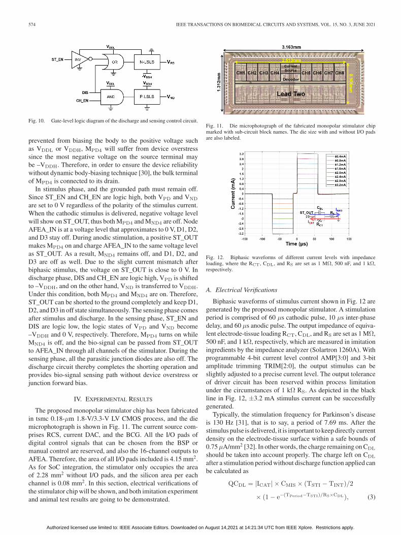
Fig. 12. Biphasic waveforms of different current levels with impedanceloading, where the RCT, CDL, and RS are set as 1 MΩ, 500 nF, and 1 kΩ,respectively.
A. Electrical Verifications
Biphasic waveforms of stimulus current shown in Fig. 12 aregenerated by the proposed monopolar stimulator. A stimulationperiod is comprised of 60 µs cathodic pulse, 10 µs inter-phasedelay, and 60 µs anodic pulse. The output impedance of equiva-lent electrode-tissue loading RCT, CDL, and RS are set as 1 MΩ,500 nF, and 1 kΩ, respectively, which are measured in imitationingredients by the impedance analyzer (Solartron 1260A). Withprogrammable 4-bit current level control AMP[3:0] and 3-bitamplitude trimming TRIM[2:0], the output stimulus can beslightly adjusted to a precise current level. The output toleranceof driver circuit has been reserved within process limitationunder the circumstances of 1 kΩ RS. As depicted in the blackline in Fig. 12, ±3.2 mA stimulus current can be successfullygenerated.
Typically, the stimulation frequency for Parkinson’s diseaseis 130 Hz [31], that is to say, a period of 7.69 ms. After thestimulus pulse is delivered, it is important to keep directly currentdensity on the electrode-tissue surface within a safe bounds of0.75µA/mm2 [32]. In other words, the charge remaining on CDL
should be taken into account properly. The charge left on CDL
after a stimulation period without discharge function applied canbe calculated as
QCDL = |ICAT| × CMIS × (TSTI − TINT)/2
× (1− e−(TPeriod−TSTI)/RS×CDL), (3)
Authorized licensed use limited to: IEEE Associate Editors. Downloaded on August 14,2021 at 14:21:34 UTC from IEEE Xplore. Restrictions apply.

HSIEH AND KER: MONOPOLAR BIPHASIC STIMULATOR WITH DISCHARGE FUNCTION AND NEGATIVE LEVEL 575
Fig. 13. Average current mismatch between cathodic/anodic stimulationpulses and extra current among five stimulator chips.
where |ICAT| × CMIS represents the extra current that causesredundant charge, TSTI, TINT, and TPeriod are the time of stim-ulus pulse interval, inter-phase delay, and stimulation period,respectively, all the timing parameters are labeled in Fig. 9(b).The exponential term explains RC discharge through spreadresistance RS and double-layer capacitance CDL. In this work,the time constant of RS and CDL is 0.5 ms. Fig. 13 shows theaverage current mismatch between the cathodic/anodic stimuluspulses of five stimulator chips, and is abbreviated as CMIS in(3). The current mismatch of all current levels is depicted as theblue line. It can be seen that the mismatch percentage is moresensitive to lower current levels, since it is calculated as theratio of |ICAT| – IANO to |ICAT|. However, the red line in Fig. 13stands for the value of the extra current, which is more importanton the safety issue. As marked in Fig. 13, the maximum extracurrent is 17.6 µA in average. Therefore, maximum charge erroron CDL is 1.056 nC. From (3), it can be found that the redundantcharge barely discharged by the impedance model itself when thestimulator is under high-Z state. The residual average dc currentwithout discharge function applied equals to QCDL divided bythe time interval of TPeriod – TSTI, and can be computed as1.056 nC × (1 – e−15.12) / 7.56 ms = 139.68 nA.
If the discharge function is activated, the node ST_OUT willbe shorted to ground, thus accelerates the discharge program.The charge left on CDL after a stimulus phase with shortingoperation can be expressed as
QCDL = |ICAT| × CMIS × (TSTI − TINT)/2
× e−TDIS/RS×CDL , (4)
Where TDIS indicates the discharge time that is given fromthe digital control. It is well known that 4 times duration ofthe time constant makes the charge reduce to 1.8% left of RCcircuit. Therefore, 2 ms of discharge time is given in this case.The residual average dc current with discharge function appliedequals to the QCDL after shorting operation divided by thetime interval of TPeriod – TSTI – TDIS, which is calculatedas 1.056 nC × 1.8% / 5.56 ms = 3.42 nA. Fig. 14 shows thecomparison of average dc current on ST_OUT that with andwithout discharge operation to the criteria in ISO 14708-1, part1 [32]. For the surface area of 5.985 mm2 (Medtronic 3389),
Fig. 14. Charge error after one stimulation period of all output current levels,and the average dc current is significantly reduced by applying dischargeoperation.
Fig. 15. (a) An oscilloscope capture of ISTI, ST_OUT, and the voltagedifference on CDL (ΔVCDL), which allows the measurement of accumulatedcharges after 10 stimulation pulses. (b) The enlarged y-axis of ΔVCDL in (a).
the limitation of safety concern can be calculated as 4489 nA. Itcan be seen that the residual average dc current is significantlyreduced by implementing the shorting operation.
Due to the small mismatch between cathodic/anodic pulses,the residual charge is within safety boundary according to ISO14708-1 even though the discharge operation is not activatedafter one stimulation. However, the redundant charge will accu-mulate until next stimulation. Fig. 15 illustrates the charge accu-mulation on CDL by delivering 10 biphasic stimuli continuously,and the voltage difference on CDL (ΔVCDL) comes to 34.63 mVat the end of the 10th stimulation, which is enlarged in Fig. 15(b).
Authorized licensed use limited to: IEEE Associate Editors. Downloaded on August 14,2021 at 14:21:34 UTC from IEEE Xplore. Restrictions apply.

576 IEEE TRANSACTIONS ON BIOMEDICAL CIRCUITS AND SYSTEMS, VOL. 15, NO. 3, JUNE 2021
Fig. 16. (a) Diagram of imitation experimental setup. (b) Experimental picturewith Medtronic 3389 electrode.
Nevertheless,ΔVCDL drops to 1.56 mV after the 2 ms dischargeis applied, which means only 0.78 nC is remaining, and theresidual dc current reduce to 2.53 nA. In addition, infer fromthe standard of 4489 nA average dc current and impedancemodel, ΔVCDL should be less than 4489 nA × 7.56 ms /500 nF = 67.8 mV during the time interval TPeriod – TSTI.Thus, 10 stimuli to 1 discharge has been proved to be safe in thiscase so that the time after the stimulus pulse can be used moreefficiently for bio-signal processing.
B. Imitation Measurements
The proposed monopolar stimulator chip is first verified inphantom gels, which mimic brain features, before it is usedin in-vivo animal test [33]. Fig. 16(a) shows the experimentalsetup for imitation measurements in detail, where the gel ismade of NaCl, agar, and deionized (DI) water with a properratio [33], and an electrode lead contains four channels. Oneside of Medtronic 3389 electrode lead was inserted into thegels, at the meantime, the other side of it was connected tothe stimulator output (ST_OUT) and the oscilloscope (DigilentAnalog Discovery 2). Fig. 16(b) is the real picture of in-vitroexperiment. When one channel delivers the stimulation pulses,the artifact of the stimulus appears on the other three channels.Hence, those disabled drivers of the stimulator are designedto tolerate artifacts causes by the enabled channel. Also, fromthe perspective of bio-signal processing, bio-signal is oftencontaminated by large saturating artifacts [34]. Therefore, thescale of the artifact is an important factor that should be takeninto consideration in neural-stimulator system development.Fig. 17(a) shows the measured results of artifact by delivering±3 mA stimulus current on CH1. It can be observed that thelargest artifact appears at the neighborhood channel with 62% ofstimulation amplitude. Although it drops to 53% on the farthestchannel, the difference between CH3 and CH4 is only 3%. Inconclusion, at least half of the stimulus magnitude will be seenon other non-stimulated channels.
In Fig. 17(b), another aspect of the imitation measurementis shown. As mentioned in the previous section, the outputvoltage of stimulator equals to ISTI multiplied by RS. Thespread resistance not only changes from case to case in differentapplications, but is also affected by the distance from ST_OUTto the ground. Fig. 17(b) shows the output waveforms that aremeasured on various ground distances. As expected, the farther
Fig. 17. Measured results in agar by delivering ±3 mA biphasic current fromthe stimulator to electrode lead CH1. (a) Artifact on CH2, CH3, and CH4. (b)Different distance between stimulator ground and electrode lead, 1 cm per stepfrom the near to the distant.
the ground is located, the larger the RS is gauged. The range ofRS various from 0.972 kΩ to 1.2 kΩ in 5 cm, i.e. about 20%deviation should be considered.
C. Animal Test
The function of the fabricated monopolar stimulator chipwas also verified with in-vivo animal experiment, which hasbeen reviewed and approved by the Institutional Animal Careand Use Committee (IACUC). Parkinson’s disease onset ofrat was induced by injecting 6-hydroxydopamine (6-OHDA).Fig. 18(a) depicts the measurement setup of the animal test.Both the stimulator output and the local field potential (LFP)of the rat are monitored on the computer by the oscilloscope(Digilent Analog Discovery 2) and the data acquisition system(ADInstruments PowerLab 4/30). Electrodes are inserted in thesubthalamic nucleus (STN). An area that is considered of themost effective in DBS treatment [9], [12], [31]. The detailconnections of the animal test is shown in Fig. 18(b), whereeach electrode lead can be divided into two wires for outputand return. One lead is for stimulation, the other is for LFP
Authorized licensed use limited to: IEEE Associate Editors. Downloaded on August 14,2021 at 14:21:34 UTC from IEEE Xplore. Restrictions apply.

HSIEH AND KER: MONOPOLAR BIPHASIC STIMULATOR WITH DISCHARGE FUNCTION AND NEGATIVE LEVEL 577
TABLE IIPERFORMANCE COMPARISON WITH RELATED PRIOR WORKS
∗The area contains only the shorting circuit. ∗∗The area contains only the current compensate circuits.ΦProvides only the mismatch current of 1.12 µA after calibration. ΦΦProvides only the voltage on stimulator output of 20 mV after calibration.
Fig. 18. (a) Diagram of animal experimental setup of local field potential (LFP)measurement that connects to proposed stimulator chip. (b) Enlarged photo fromtop of the rat head with electrodes implanted.
recording. In this case, the stimulator return is connected toground for monopolar stimulation. Besides, the LFP reference isalso grounded through the amplifier (Grass Instruments P511K).In Fig. 19, one minute of LFP signal is recorded, which consistsof 20 s before stimulation, 20 s of current stimulation, and 20 s
Fig. 19. Measured data of LFP and electrical stimulation. Recording LFPfrom rat onset of Parkinson’s disease before stimulation and after stimulation.The power spectrum peak of beta band can be successfully supressed by theproposed monopolar biphasic stimulus currrent of ±0.2 mA.
after stimulation. Due to the tiny size of rat STN, the current of±0.2 mA is applied under 130 Hz, which can be measured onboth data acquisition and scope. The spectral power of beta band(12-30 Hz) is an important sign to diagnose Parkinson’s disease[9], [31]. It can be seen that beta band peaks appear at 21.5 Hzand 24.4 Hz before stimulation. After biphasic current pulsesare delivered, beta band peaks are suppressed successfully.
V. CONCLUSION
A 16-channel monopolar biphasic stimulus circuit with dis-charge function has been designed and fabricated in a 0.18-µm1.8V/3.3V CMOS process. With common grounded p-substrateand the area of 0.08 mm2 per channel, the stimulator is ben-eficial to SoC integration with analog acquisition circuits and
Authorized licensed use limited to: IEEE Associate Editors. Downloaded on August 14,2021 at 14:21:34 UTC from IEEE Xplore. Restrictions apply.

578 IEEE TRANSACTIONS ON BIOMEDICAL CIRCUITS AND SYSTEMS, VOL. 15, NO. 3, JUNE 2021
digital bio-signal processor together for implantable biomedicaldevices. Without suffering the device overstress or p-n junctionbreakdown issue, the maximum stimulus current of ±3 mAcan be generated under 12-V compliance voltage. Performancecomparisons among the prior works are shown in Table II.The calibration techniques often contain extra circuits such ascomparator or ADC, which lead to power and area inefficiency.The proposed discharge circuit can keep the maximum averageresidual dc current under 3.42 nA with two transistors. It hasbeen proved that the stimulator is able to suppress the beta bandeffectively through in vivo animal test. With the programmablecontrol signals, the developed stimulator is flexible for biomed-ical applications.
ACKNOWLEDGMENT
The authors would like to thank Taiwan Semiconductor Re-search Institute (TSRI) for the support of chip design EDA Toolsand silicon fabrication via TSMC.
REFERENCES
[1] C.-Y. Wu et al., “Design considerations and clinical applications of closed-loop neural disorder control SoCs,” in Proc. IEEE 22nd Asia South PacificDes. Automat., 2017, pp. 295–298, doi: 10.1109/ASPDAC.2017.7858337.
[2] F.-G. Zeng, S. Rebscher, W. Harrison, X. Sun, and H. Feng, “Cochlearimplants: system design, integration, and evaluation,” IEEE Rev. Biomed.Eng., vol. 1, pp. 115–142, Nov. 2008, doi: 10.1109/RBME.2008.2008250.
[3] B. Geng, J. Dong, W. Jensen, S. Dosen, D. Farina, and E. N.Kamavuako, “Psychophysical evaluation of subdermal electrical stim-ulation in relation to prosthesis sensory feedback,” IEEE Trans. Neu-ral Syst. Rehabil. Eng., vol. 26, no. 3, pp. 709–715, Mar. 2018, doi:10.1109/TNSRE.2018.2803844.
[4] S.-P. Lin and M.-D. Ker, “Design of multiple-charge-pump system forimplantable biomedical applications,” in Proc. IEEE Biomed. Circuits Syst.Conf. (BioCAS), 2018, pp. 1–4, doi: 10.1109/BIOCAS.2018.8584758.
[5] Z. Luo, L.-C. Yu, and M.-D. Ker, “An efficient, wide-output, high-voltagecharge pump with a stage selection circuit realized in a low-voltage CMOSprocess,” IEEE Trans. Circuits Syst. I, Regular Papers, vol. 66, no. 9,pp. 3437–3444, Sep. 2019, doi: 10.1109/TCSI.2019.2924581.
[6] S.-P. Lin and M.-D. Ker, “Design of stage-selective negative voltagegenerator to improve on-chip power conversion efficiency for neuronstimulation,” IEEE Trans. Circuits Syst. I, Regular Papers, vol. 67, no. 11,pp. 4122–4131, Nov. 2020, doi: 10.1109/TCSI.2020.3012086.
[7] J. Zhao, L. Yao, R.-F. Xue, P. Li, M. Je, and Y. P. Xu, “An integratedwireless power management and data telemetry IC for high-compliance-voltage electrical stimulation applications,” IEEE Trans. Biomed. Cir-cuits Syst., vol. 10, no. 1, pp. 113–124, Feb. 2016, doi: 10.1109/TB-CAS.2015.2404038.
[8] M. H. Maghami, A. M. Sodagar, and M. Sawan, “Versatile stimulationback-end with programmable exponential current pulse shapes for a retinalvisual prosthesis,” IEEE Trans. Neural Syst. Rehabil. Eng., vol. 24, no. 11,pp. 1243–1253, Nov. 2016, doi: 10.1109/TNSRE.2016.2542112.
[9] T. M. Herrington, J. J. Cheng, and E. N. Eskandar, “Mechanisms of deepbrain stimulation,” J. Neurophysiol., vol. 115, no. 1, pp. 19–38, Jan. 2015,doi: 10.1152/jn.00281.2015.
[10] C. P. Warren, S. Hu, M. Stead, B. H. Brinkmann, M. R. Bower, and G.A. Worrell, “Synchrony in normal and focal epileptic brain: the seizureonset zone is functionally disconnected,” J. Neurophysiol., vol. 104, no. 6,pp. 3530–3539, Dec. 2010, doi: 10.1152/jn.00368.2010.
[11] C.-Y. Wu et al., “CMOS 256-pixel/480-pixel photovoltaic-powered sub-retinal prosthetic chips with wide image dynamic range and bi/four-directional sharing electrodes and their ex vivo experimental validationswith mice,” IEEE Trans. Circuits Syst. I, Regular Papers, vol. 67, no. 10,pp. 3273–3282, Oct. 2020, doi: 10.1109/TCSI.2020.2976716.
[12] S. Little et al., “Adaptive deep brain stimulation in advanced Parkinsondisease,” Ann. Neurol., vol. 74, no. 3, pp. 449–457, Sep. 2013, doi:10.1002/ana.23951.
[13] M. Mohr, T. Schon, V. Tscharner, and B. M. Nigg, “Intermuscular co-herence between surface EMG signals is higher for monopolar comparedto bipolar electrode configurations,” Front. Physiol., vol. 9, pp. 566–579,May 2018, doi: 10.3389/fphys.2018.00566.
[14] M. J. Krenn, J. L. V. Luna, W. Mayr, and D. S. Stokic, “Bipolartranscutaneous spinal stimulation evokes short-latency reflex responsesin human lower limbs alike standard unipolar electrode configura-tion,” J. Neurophysiol., vol. 124, no. 4, pp. 1072–1082, Oct. 2020, doi:10.1152/jn.00433.2020.
[15] M. Gerhardt, G. Groeger, and N. MacCarthy, “Monopolar vs. bipolarsubretinal stimulation–an in vitro study,” J. Neurosci. Methods, vol. 199,no. 1, pp. 26–34, Jul. 2011, doi: 10.1016/j.jneumeth.2011.04.017.
[16] S. F. Cogan, “Neural stimulation and recording electrodes,”Annu. Rev. Biomed. Eng., vol. 10, pp. 275–309, Apr. 2008, doi:10.1146/annurev.bioeng.10.061807.160518.
[17] A. Zhou, B. C. Johnson, and R. Muller, “Toward true closed-loop neuro-modulation: artifact-free recording during stimulation,” Curr. Opin. Neu-robiol., vol. 50, pp. 119–127, Jun. 2018, doi: 10.1016/j.conb.2018.01.012.
[18] K. Sooksood, T. Stieglitz, and M. Ortmanns, “An active approachfor charge balancing in functional electrical stimulation,” IEEE Trans.Biomed. Circuits Syst., vol. 4, no. 3, pp. 162–170, Jun. 2010, doi:10.1109/TBCAS.2010.2040277.
[19] S. Oh et al., “Light-controlled biphasic current stimulator IC using CMOSimage sensors for high-resolution retinal prosthesis and in vitro experi-mental results with rd1 mouse,” IEEE Trans. Biomed. Eng., vol. 62, no. 1,pp. 70–79, Jan. 2015, doi: 10.1109/TBME.2014.2336799.
[20] Z. Luo and M.-D. Ker, “A high-voltage-tolerant and precise charge-balanced neuro-stimulator in low voltage CMOS process,” IEEE Trans.Biomed. Circuits Syst., vol. 10, no. 6, pp. 1087–1099, Dec. 2016, doi:10.1109/TBCAS.2015.2512443.
[21] M. Monge et al., “A fully intraocular high-density self-calibrating epireti-nal prosthesis,” IEEE Trans. Biomed. Circuits Syst., vol. 7, no. 6,pp. 747–760, Dec. 2013, doi: 10.1109/TBCAS.2014.2298334.
[22] N. Butz, A. Taschwer, S. Nessler, Y. Manoli, and M. Kuhl, “A 22 Vcompliant 56 µW twin-track active charge balancing enabling 100%charge compensation even in monophasic and 36% amplitude correctionin biphasic neural stimulators,” IEEE J. Solid-State Circuits, vol. 53, no. 8,pp. 2298–2310, Aug. 2018, doi: 10.1109/JSSC.2018.2828823.
[23] H. Chun, Y. Yang, and T. Lehmann, “Safety ensuring retinal prosthesis withprecise charge balance and low power consumption,” IEEE Trans. Biomed.Circuits Syst., vol. 8, no. 1, pp. 108–118, Feb. 2014, doi: 10.1109/TB-CAS.2013.2257171.
[24] Y. T. Wong et al., “Retinal neurostimulator for a multifocal vision prosthe-sis,” IEEE Trans. Neural Syst. Rehabil. Eng., vol. 15, no. 3, pp. 425–434,Sep. 2007, doi: 10.1109/TNSRE.2007.903958.
[25] V. Valente, A. Demosthenous, and R. Bayford, “A tripolar current-steeringstimulator ASIC for field shaping in deep brain stimulation,” IEEETrans. Biomed. Circuits Syst., vol. 6, no. 6, pp. 197–207, Jun. 2012, doi:10.1109/TBCAS.2011.2171036.
[26] C.-C. Chen and K.-T. Tang, “A 12 V-500 µA neuron stimulator withcurrent calibration mechanism in 0.18 µm standard CMOS process,” inProc. IEEE Biomed. Circuits Syst. Conf. (BioCAS), 2011, pp. 57–60, doi:10.1109/BioCAS.2011.6107726.
[27] P. Liu, X. Wang, D. Wu, Z. Zhang, and L. Pan, “A novel high-speed andlow-power negative voltage level shifter for low voltage applications,” inProc. IEEE Int. Symp. Circuits Syst. (ISCAS), 2010, pp. 601–604, doi:10.1109/ISCAS.2010.5537521.
[28] Y. E. Tsiatouhas, “A stress-relaxed negative voltage-level converter,” IEEETrans. Circuits Syst. II, Exp. Briefs, vol. 54, no. 3, pp. 282–286, Mar. 2007,doi: 10.1109/TCSII.2006.886877.
[29] H.-W. Chiu et al., “Pain control on demand based on pulsed radio-frequency stimulation of the dorsal root ganglion using a batterylessimplantable CMOS SoC,” IEEE Trans. Biomed. Circuits Syst., vol. 4, no. 6,pp. 350–359, Dec. 2010, doi: 10.1109/TBCAS.2010.2081668.
[30] J. Qin, S. Chen, C. Guo, and Y. Du, “Simulation study of the single-eventeffects sensitivity in nanoscale CMOS for body-biasing circuits,” IEEETrans. Device Mater. Rel., vol. 14, no. 2, pp. 639–644, Jun. 2014, doi:10.1109/TDMR.2014.2308592.
[31] J. K. Krauss et al., “Technology of deep brain stimulation: current statusand future directions,” Nat. Rev. Neurol., vol. 17, pp. 75–87, Nov. 2020,doi: 10.1038/s41582-020-00426-z.
[32] Implants for surgery—Active implantable medical devices—Part 1: Gen-eral requirements for safety, marking and for information to be providedby the manufacturer, Standard ISO 14708-1:2014(E), International Orga-nization for Standardization, Geneva, Switzerland, 2014.
Authorized licensed use limited to: IEEE Associate Editors. Downloaded on August 14,2021 at 14:21:34 UTC from IEEE Xplore. Restrictions apply.

HSIEH AND KER: MONOPOLAR BIPHASIC STIMULATOR WITH DISCHARGE FUNCTION AND NEGATIVE LEVEL 579
[33] M. A. Kandadai, J. L. Raymond, and G. J. Shaw, “Comparison of electricalconductivities of various brain phantom gels: developing a ‘brain gelmodel’,” Mater. Sci. Eng. C, vol. 32, no. 8, pp. 2664–2667, Dec. 2012,doi: 10.1016/j.msec.2012.07.024.
[34] S. Qiu et al., “A stimulus artifact removal technique for SEMG sig-nal processing during functional electrical stimulation,” IEEE Trans.Biomed. Eng., vol. 62, no. 8, pp. 1959–1968, Aug. 2015, doi:10.1109/TBME.2015.2407834.
[35] K. Chen, Z. Yang, L. Hoang, J. Weiland, M. Humayun, andW. Liu, “An integrated 256-channel epiretinal prosthesis,” IEEE J.Solid-State Circuits, vol. 45, no. 9, pp. 1946–1956, Sep. 2010, doi:10.1109/JSSC.2010.2055371.
Chia-Chi Hsieh received the B.S. degree from theDepartment of Electrical and Computer Engineering,National Chiao Tung University (NCTU), Hsinchu,Taiwan, in 2016, and the M.S. degree from the Insti-tute of Electronics, NCTU, in 2018. She is currentlyworking toward the Ph.D. degree on the topic of ana-log circuit design for biomedical applications with theInstitute of Electronics, National Yang Ming ChiaoTung University, Hsinchu, Taiwan.
Ming-Dou Ker (Fellow, IEEE) received the Ph.D.degree from the Institute of Electronics, NationalChiao Tung University, Hsinchu, Taiwan, in 1993.He is currently a Distinguished Professor with theInstitute of Electronics, National Yang Ming ChiaoTung University (NYCU), Hsinchu, Taiwan, and alsothe Director at Biomedical Electronics TranslationalResearch Center, NYCU, working on biomedicalelectronics translational projects. In the technical fieldof reliability and quality design for microelectroniccircuits and systems, he has authored or coauthored
more than 590 technical papers in international journals and conferences. Hehas proposed many solutions to improve the reliability and quality of integratedcircuits, which have been granted with hundreds of U.S. patents. His currentresearch interests include the circuits and systems for biomedical applications,and circuit-related reliability issue. He was a Member of the Technical ProgramCommittee and the Session Chair of numerous international conferences formany years, including IEEE Symposium on VLSI Circuits, IEEE Interna-tional Symposium on Circuits and Systems (ISCAS), and IEEE InternationalSolid-State Circuits Conference. He was an Associate Editor for the IEEETRANSACTIONS ON VLSI SYSTEMS, Associate Editor for the IEEE TRANSAC-TIONS ON BIOMEDICAL CIRCUITS AND SYSTEMS, and the Guest Editor of theISCAS2019 Special Issue in IEEE TRANSACTIONS ON BIOMEDICAL CIRCUITS
AND SYSTEMS. He is the Editor of the IEEE TRANSACTION ON DEVICE AND
MATERIALS RELIABILITY, and the Guest Editor of the Frontiers in Neuroscienceon the research topic of microelectronic implants for central and peripheralnervous system.
Authorized licensed use limited to: IEEE Associate Editors. Downloaded on August 14,2021 at 14:21:34 UTC from IEEE Xplore. Restrictions apply.