monopole antenna arrays for optical trapping, … antenna arrays for optical trapping, spectroscopy,...
TRANSCRIPT
Monopole antenna arrays for optical trapping, spectroscopy, and sensingA. E. Çetin,1 Ahmet Ali Yanik,1 Cihan Yilmaz,2 Sivasubramanian Somu,2
Ahmed Busnaina,2 and Hatice Altug1,a�
1Department of Electrical and Computer Engineering, Boston University, Boston, Massachusetts 02215,USA and Photonics Center, Boston University, Boston, Massachusetts 02215, USA2NSF Nanoscale Science and Engineering Center for High-rate Nanomanufacturing,Northeastern University, Boston, Massachusetts 02215, USA
�Received 21 December 2010; accepted 3 February 2011; published online 17 March 2011�
We introduce a nanoplasmonic platform merging multiple modalities for optical trapping,nanospectroscopy, and biosensing applications. Our platform is based on surface plasmon polaritondriven monopole antenna arrays combining complementary strengths of localized and extendedsurface plasmons. Tailoring of spectrally narrow resonances lead to large index sensitivities �S�675 nm /RIU� with record high figure of merits �FOM�112.5�. These monopole antennassupporting strong light localization with easily accessible near-field enhanced hotspots are suitablefor vibrational nanospectroscopy and optical trapping. Strong optical forces �350 pN /W /�m2� areshown at these hotspots enabling directional control with incident light polarization. © 2011American Institute of Physics. �doi:10.1063/1.3559620�
Surface confinement of light through propagating andlocalized surface plasmons �SPs� holds great promise for ap-plications in biosensing,1,2 nanospectroscopy,3–5 and opticaltrapping of bioparticles.6,7 Within the past decade, manygroundbreaking observations are demonstrated using metal-lic nanostructures. Plasmonic biosensors with high multi-plexing characteristics are shown.8 Ultrasensitive vibrationalnanospectroscopy down to zepto-mole levels of proteins isdemonstrated by using surface enhanced absorption signalsamplified with collective plasmonic excitations.9 Low-powerplasmonic tweezers with minute trapping volumes well be-low the diffraction limited volume of light are realized withlow power laser sources.10 However, most of these plas-monic structures serve for a single operational purpose. Forexample, biosensing platforms based on effective refractiveindex modulation are not very suitable for spectroscopic ap-plications since the near-field enhancements are relativelysmaller than the nanoparticle based approaches with sharpstructural features. On the other hand, plasmonic structuresused for nanoparticle trapping are equipped with high gradi-ent electromagnetic near-fields suitable for creating largetransverse gradient forces, but lack spectrally sharp resonantbehavior needed for sensing applications.
In this letter, we present a plasmonic platform mergingmultiple modalities by bringing complementary characteris-tics of localized and extended SPs together. The proposedplatform, based on periodic arrays of nanopillars on a singlemetal sheet, allows enhanced device performances for bio-sensing, nanospectroscopy, and optical trapping applicationsat the same time. We achieve high refractive index sensitivi-ties �S�675 nm /RIU� with large figure of merits �FOM�112.5� for detection limits. Such large figures are attrib-uted to tight localization of plasmonic excitations in nanopil-lar structures leading to spectrally narrow resonances. Plas-monic hot spots created at the tips of the nanopillarstructures are easily accessible by biochemical analytes,which is important for ultrasensitive spectroscopic measure-ments and optical trapping of nanoparticles with low power
excitation sources. Polarization dependent optical forcegradient enabled by the nanopillar arrays also provides theability to control the direction of the trapping force. Thisplatform, allowing optical trapping of bioparticles and simul-taneous measurement of spectroscopic signatures and realtime biodetection events, could find wide range of applica-tions in sensing applications.
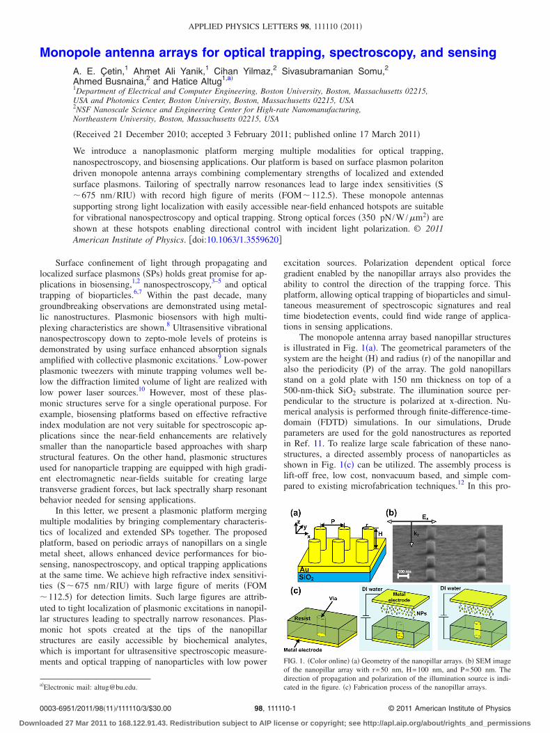
The monopole antenna array based nanopillar structuresis illustrated in Fig. 1�a�. The geometrical parameters of thesystem are the height �H� and radius �r� of the nanopillar andalso the periodicity �P� of the array. The gold nanopillarsstand on a gold plate with 150 nm thickness on top of a500-nm-thick SiO2 substrate. The illumination source per-pendicular to the structure is polarized at x-direction. Nu-merical analysis is performed through finite-difference-time-domain �FDTD� simulations. In our simulations, Drudeparameters are used for the gold nanostructures as reportedin Ref. 11. To realize large scale fabrication of these nano-structures, a directed assembly process of nanoparticles asshown in Fig. 1�c� can be utilized. The assembly process islift-off free, low cost, nonvacuum based, and simple com-pared to existing microfabrication techniques.12 In this pro-
a�Electronic mail: [email protected].
FIG. 1. �Color online� �a� Geometry of the nanopillar arrays. �b� SEM imageof the nanopillar array with r=50 nm, H=100 nm, and P=500 nm. Thedirection of propagation and polarization of the illumination source is indi-cated in the figure. �c� Fabrication process of the nanopillar arrays.
APPLIED PHYSICS LETTERS 98, 111110 �2011�
0003-6951/2011/98�11�/111110/3/$30.00 © 2011 American Institute of Physics98, 111110-1
Downloaded 27 Mar 2011 to 168.122.91.43. Redistribution subject to AIP license or copyright; see http://apl.aip.org/about/rights_and_permissions
cess, initially, gold layer is deposited on a glass substrate.Subsequently, nanoscale vias are fabricated with conven-tional electron-beam nanolithography using poly-methylmethacrylate �PMMA� resist. Then, metallic nanoparticlessuspended in de-ionized �DI� water are precisely assembledinto the vias by applying an electric field between the fixedbottom electrode and a top counter electrode placed far awayfrom the resist. The dimension of fabricated nanopillars iscontrolled by the size of the vias. During the assembly pro-cess, nanoparticles are fused due to the current passingthrough them resulting in nanopillar formation in the vias. Asa final step in the fabrication, the resist is dissolved usingacetone. With this process, we can fabricate tall as well ashigh-aspect ratio nanopillars. Figure 1�b� shows scanningelectron microscope �SEM� image of a preliminary result ofa fabricated nanopillar array �r=50 nm, H=100 nm, and P=500 nm� employing the directed assembly process. Thefabrication of a three-dimensional �3D� nanopillar array plat-form for optical measurements needs further developmentsto scale the nanopillar height to the optimized values.
Figure 2�a� shows the strong role of the localized and theextended SP couplings in periodic nanopillar array response.In periodic arrays, two resonance dips in the reflection spec-tra are observed corresponding to excitation of the SP polari-tons �SPPs� by different grating orders. The relativelysharper and stronger resonance dip observed at longer wave-lengths is due to the monopole antenna behavior of the nano-pillar structure driven by the Au/DI�1,0� SPP excitation. Theweaker resonance dip, on the other hand, is due to the exci-tation of the Au/DI�1,1� mode. It is also important to notethat our nanopillar array is excited with perpendicularly illu-minated light source. Unlike previous offerings based onprism coupling, this collinear arrangement enables massivemultiplexing with minimal alignment requirements.3 For thesingle nanopillar structure, resonances are not observable dueto the weak coupling of the directly incident light. This ob-servation proves the important role of SPPs in excitation ofstrong monopole antenna resonances in these structures. Fig-ure 2�b� shows the radius dependence of resonance behavior
of nanopillar arrays for a fixed height �H=400 nm� in DIwater �n=1.33�. Structures with small radiuses, i.e., r=50 nm, exhibit weak resonance behaviors, since the polar-izability of the small nanopillars is relatively weaker. As theradius of the nanopillars increases, larger polarizability of thepillars enables stronger coupling of the SPPs to localized SPs�LSPs�. An optimum resonance behavior with a spectrallysharp reflectance dip is observed when the radius of thestructures is r=100 nm. Further increasing of nanopillar ra-dius leads to redshifting in both Au/DI�1,0� and Au/DI�1,1�resonance modes as the LSPs shift to longer wavelengths.However, larger dimensions also lead to broader resonancesdue to increased losses.
As shown in Fig. 2�c�, increasing height of the nano-structures �with a fixed radius of r=100 nm� results in red-shifting in the plasmonic resonance dips. Optimum monopo-lar antenna behavior with nearly zero reflectance is observedwhen the height of the nanopillars is H=400 nm. As thelength of the nanopillars further increases, the resonance getsbroadened and reflectance dips become smaller. In the fol-lowing analysis, nanopillar arrays with r=100 nm and H=400 nm are used since the best monopole antenna behaviorwith minimum reflectance and narrowest resonance linewidths is observed for these structure parameters. The fabri-cation scheme described above is suitable for achieving theproposed structure. An optimized periodicity P=600 nm re-sulted with the sharpest resonance behavior. Figure 2�d�shows the resonance shifts for varying indexes of bulk solu-tions for the optimized arrays. As large as 675 nm/RIU �S=�� /�n� refractive index sensitivity is achieved for thesestructures. For the optimized structure with spectrally narrowresonances �FWHM=6 nm�, we showed that FOMs can beas large as 112.5. These values are more an order of magni-tude larger than the previously recorded FOMs for nanopar-ticle and metamaterial sensors based on localized SPs.13,14
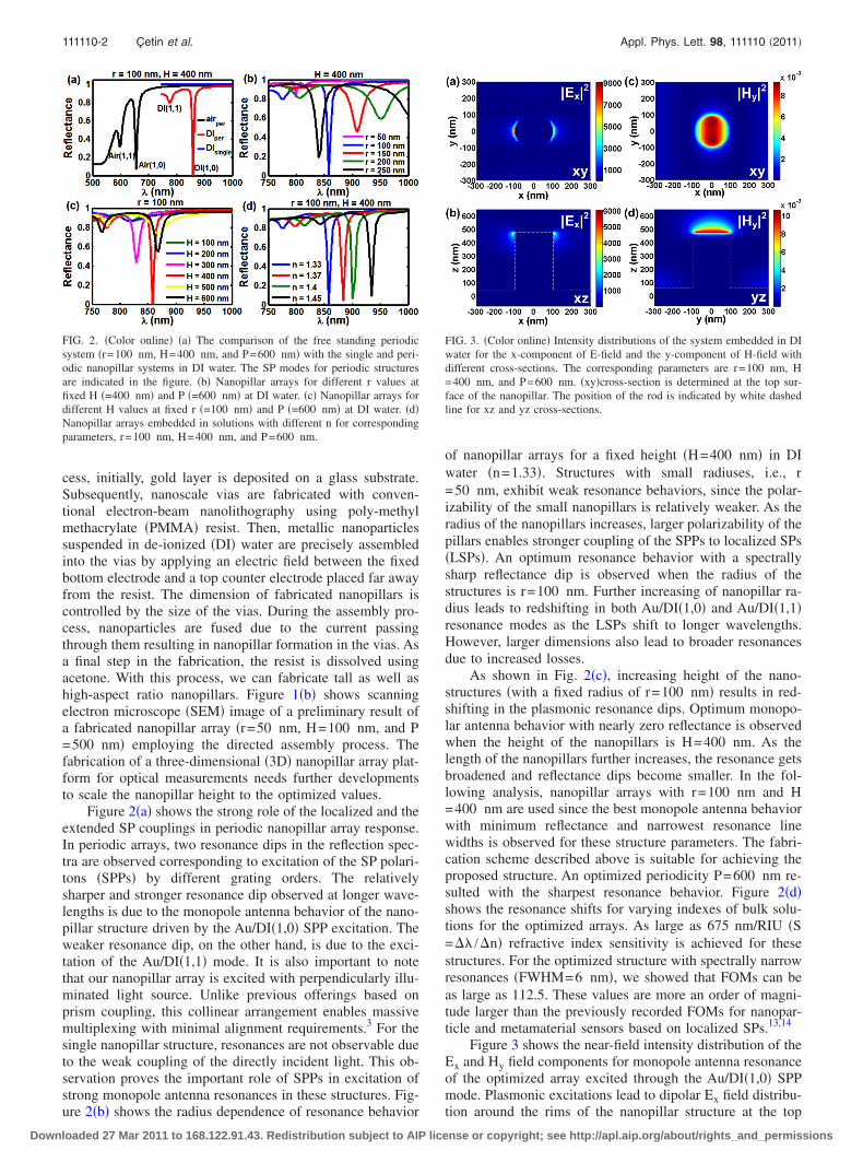
Figure 3 shows the near-field intensity distribution of theEx and Hy field components for monopole antenna resonanceof the optimized array excited through the Au/DI�1,0� SPPmode. Plasmonic excitations lead to dipolar Ex field distribu-tion around the rims of the nanopillar structure at the top
FIG. 2. �Color online� �a� The comparison of the free standing periodicsystem �r=100 nm, H=400 nm, and P=600 nm� with the single and peri-odic nanopillar systems in DI water. The SP modes for periodic structuresare indicated in the figure. �b� Nanopillar arrays for different r values atfixed H �=400 nm� and P �=600 nm� at DI water. �c� Nanopillar arrays fordifferent H values at fixed r �=100 nm� and P �=600 nm� at DI water. �d�Nanopillar arrays embedded in solutions with different n for correspondingparameters, r=100 nm, H=400 nm, and P=600 nm.
FIG. 3. �Color online� Intensity distributions of the system embedded in DIwater for the x-component of E-field and the y-component of H-field withdifferent cross-sections. The corresponding parameters are r=100 nm, H=400 nm, and P=600 nm. �xy�cross-section is determined at the top sur-face of the nanopillar. The position of the rod is indicated by white dashedline for xz and yz cross-sections.
111110-2 Çetin et al. Appl. Phys. Lett. 98, 111110 �2011�
Downloaded 27 Mar 2011 to 168.122.91.43. Redistribution subject to AIP license or copyright; see http://apl.aip.org/about/rights_and_permissions

surface with enhancement factors close to 9000 �Fig. 3�a��.Monopolar antenna behavior is clearly observable in the xz-cross sectional field profile cutting through the center of thisstructure �Fig. 3�b��. As shown in Figs. 3�c� and 3�d�, near-field profile of Hy field component demonstrates strong near-field enhancements on the top surface of the pillar structurepenetrating into the dielectric medium right above it. Strongnear-field intensities extending into medium are ideal for en-hanced vibrational spectroscopy applications as we can havemaximum overlap between the analyte and the optical field.This characteristic is also highly suitable for optical trapping.
Optical forces can be obtained by integrating Maxwellstress tensor over an area surrounding a nanoparticle. In Figs.4�a� and 4�b�, 3D and two-dimensional �2D� illustrations arepresented for three different locations of a dielectric spheri-cal bead �radius 50 nm� where the optical forces are calcu-lated within the near field of pillar structure. For all configu-rations, the center of the bead is positioned 200 nm above thetop surface of the nanopillar structure �in z-direction�. Thex-y locations are chosen in a way that the bead is locatedalways on an arc �radius 200 nm� centered at the nanopillaraxis. Subsequently, the following three settings are chosen:�i� bead is located on the y-axis �blue colored�. �ii� bead islocated on the diagonal of the x-y axes �red colored�. �iii�bead is located on the x-axis �black colored�. In Fig. 4�c�,different components of the optical forces acting on a beadare compared for different locations. Due to the dipolar modecharacter of the nanopillar LPs, the near-field gradients aresymmetric in the x-direction when illuminated with anx-polarized light source. Hence, Fx component is zero for abead located at �i�. Similarly, Fy component is zero for abead located at �iii�. Both x- and y-direction force compo-nents exist for a bead located on the diagonal �ii�. The stron-ger optical force in the y-direction �Fx�Fy� pulls the diago-nally located bead �ii� toward the hotspot where the near-field gradients are expected to be largest. The strongestoptical force is obtained once the bead is located at �iii� withFz=350 pN /W /�m2, due to the direction of the propagationand the polarization of the illumination source. The ability tocontrol the locations of the hotspots with the polarization ofthe incident light source also allows tunability of the opticalgradient force. This strong and directional optical force canbe utilized for optical trapping applications with polarizationcontrol.
In conclusion, we present a periodic gold nanopillar sys-tem merging multiple modalities by bringing complementarycharacteristics of localized and extended SPs together. Theproposed platform which allows light coupling through theperpendicularly incident light could be advantageous formultiplexing applications. The platform enables high refrac-tive index sensing measurements �675 nm/RIU� with verysharp resonance behavior �FWHM=6 nm�. As a result, itoffers large FOMs �FOM=112.5�, which is an order of mag-nitude larger than the previously recorded FOMs for nano-particle and metamaterial sensors based on localized SPs.Large near-field intensities �with enhancement factors closeto 9000� that are easily accessible to biochemical analytesare shown for surface enhanced Raman spectroscopy mea-
surements. Strong optical forces as high as 350 pN /W /�m2
are achieved around the hotspots. These strong and direc-tional forces around the hotspots also allow directional con-trol of the optical forces with the incident light polarization.Our platform, integrating multiple sensing modalities, in-cluding biosensing, spectroscopy and optical trapping in acompact form could find wide range of applications.
This work is supported by National Science FoundationCAREER Award �ECCS-0954790� Engineering ResearchCenter on Smart Lighting �EEC-0812056�, NSF Grant No.0832785, as well as by ONR Young Investigator Award,Massachusetts Life Science Center New Investigator Award.Authors acknowledge Kostas Research Center at Northeast-ern University and Boston University Photonics Center.
1A. V. Kabashin, Nature Mater. 8, 867 �2009�.2A. A. Yanik, M. Huang, A. Artar, T.-Y. Chang, and H. Altug, Appl. Phys.Lett. 96, 021101 �2010�.
3V. Liberman, C. Yilmaz, T. M. Bloomstein, S. Somu, Y. Echegoyen, A.Busnaina, S. G. Cann, K. E. Krohn, M. F. Marchant, and M. Rothschild,Adv. Mater. �Weinheim, Ger.� 22, 4298 �2010�.
4Z. Huang, G. Meng, Q. Huang, Y. Yanh, and C. Zhu, Adv. Mater. �Wein-heim, Ger.� 22, 4136 �2010�.
5S. Wang, D. F. P. Pile, C. Sun, and X. Zhang, Nano Lett. 7, 1076 �2007�.6L. Huang, S. J. Maerkl, and O. J. F. Martin, Opt. Express 17, 6018 �2009�.7V. D. Miljkovic, T. Pakizeh, B. Sepulveda, P. Johansson, and M. Kall, J.Phys. Chem. C 114, 7472 �2010�.
8J. N. Anker, W. P. Hall, O. Lyandres, N. C. Shah, J. Zhao, and R. P. V.Duyne, Nature Mater. 7, 442 �2008�.
9R. Adato, A. A. Yanik, J. J. Amsden, D. L. Kaplan, F. G. Omenetto, M. K.Hong, S. Erramilli, and H. Altug, Proc. Natl. Acad. Sci. U.S.A. 106,19227 �2009�.
10A. N. Grigorenko, N. W. Roberts, M. R. Dickinson, and Y. Zhang, Nat.Photonics 2, 365 �2008�.
11E. D. Palik, Handbook of Optical Constants of Solids �Academic, Orlando,FL, 1985�.
12C. Yilmaz, T.-H. Kim, S. Somu, and A. Busnaina, IEEE Trans. Nanotech-nol. 9, 653 �2010�.
13N. A. Mirin, K. Bao, and P. Nordlander, J. Phys. Chem. A 113, 4028�2009�.
14H. Liao, C. L. Nehl, and J. H. Hafner, Nanomedicine 1, 201 �2006�.
FIG. 4. �Color online� �a� 3D-schematic view of the structure with threebeads with n=1.5 positioned differently inserted in DI-water. �b� 2D-view ofthe structure with the beads. �c� x-, y-, and z-component of the opticalgradient force for three beads. The corresponding parameters are r=100 nm, H=400 nm, and P=600 nm.
111110-3 Çetin et al. Appl. Phys. Lett. 98, 111110 �2011�
Downloaded 27 Mar 2011 to 168.122.91.43. Redistribution subject to AIP license or copyright; see http://apl.aip.org/about/rights_and_permissions