morphology and electrical characteristics of p-type zno
TRANSCRIPT
RSC Advances
PAPER
Ope
n A
cces
s A
rtic
le. P
ublis
hed
on 1
2 O
ctob
er 2
018.
Dow
nloa
ded
on 1
1/26
/202
1 12
:48:
46 P
M.
Thi
s ar
ticle
is li
cens
ed u
nder
a C
reat
ive
Com
mon
s A
ttrib
utio
n 3.
0 U
npor
ted
Lic
ence
.
View Article OnlineView Journal | View Issue
Morphology and
aState Key Laboratory of High Power Semic
Science and Technology, No. 7186 Wei-Xi
Republic of China. E-mail: zouyg@cust.
85583395bState Key Laboratory of Luminescence an
Optics, Fine Mechanics and Physics, Ch
Dongnanhu Road, Changchun, 130033, PeocInstitute of Atomic and Molecular Physics,
Changchun, 130012, People's Republic of C
† Electronic supplementary informa10.1039/c8ra07135g
Cite this: RSC Adv., 2018, 8, 35023
Received 27th August 2018Accepted 3rd October 2018
DOI: 10.1039/c8ra07135g
rsc.li/rsc-advances
This journal is © The Royal Society of C
electrical characteristics of p-typeZnO microwires with zigzag rough surfacesinduced by Sb doping†
Linlin Shi, a Luchao Du,c Yingtian Xu,a Liang Jin,a He Zhang,a Yan Li,a Xiaohui Ma,a
Yonggang Zou *a and Dongxu Zhaob
Sb-doped p-type ZnO microwires with zigzag rough surfaces were synthesized by two zone chemical
vapor deposition. The zigzag morphology characteristics analyzed by high resolution scanning electron
microscopy and transmission electron microscopy show the existence of surface defects caused by Sb
doping. The incorporation of Sb into a ZnO lattice induces lattice imperfection, which is the origin of the
zigzag rough surface. Photoluminescence and electrical properties of the obtained Sb-doped ZnO
microwires were determined. The crossed structure microwire-based p–n homojunction device was
fabricated by applying as-synthesized Sb-doped p-type ZnO microwires and undoped n-type ZnO
microwires. The doped microwires demonstrate reproducible p-type conduction and enhanced
rectifying behavior with increasing Sb doping concentration. The results demonstrated that the
optimizable optical and electrical characteristics, controlled by increasing the doping concentration, are
reflected in the surface morphology changes which would be helpful for characterizing the doping
effects in micro/nanoscale materials.
Introduction
Single crystalline metal oxide semiconductor micro/nanomaterials have been utilized as building blocks in manyphotonic and electronic applications.1–3 Because of their supe-rior properties, such as multi-functionality, high crystallinity,quantum size effects, high transparency, and stability in air,micro/nanomaterials can act as future electronic materialalternatives to bulk materials. ZnO is one of the promisingmaterials for the fabrication of optoelectronic devices operatingin the blue and ultraviolet regions because of the wide directband gap (3.37 eV) and large exciton binding energy (60 mV).4,5
p-Type doping in ZnO is essential for device applications tomeet the increasing needs of present applications, and enor-mous efforts have been dedicated to the doping of ZnO withselective elements to fabricate homojunction devices, whichhave the advantages of high sensitivity, fast response speed, and
onductor Laser, Changchun University of
ng Road, Changchun, 130022, People's
edu.cn; Fax: +86-85583395; Tel: +86-
d Applications, Changchun Institute of
inese Academy of Sciences, No. 3888
ple's Republic of China
Jilin University, No. 2699 Qian-Jin Road,
hina
tion (ESI) available. See DOI:
hemistry 2018
high stability in various environments.6,7 However reports basedon the homojunction devices of ZnO nanostructure are rela-tively rare; stable and reproducible p-type doping of ZnO is stilla great challenge.8–11 Much effort has been made to obtain highquality p-type ZnO, it had been reported that Sb element witha large atom size is a good choice of ZnO dopant.12–14 Sb atomwould substitute for a Zn atom and simultaneously produce twocorresponding Zn vacancies, therefore Sb-doped ZnO showsstrong p-type conduction based on rst-principles calculation,15
hence large-mismatched Sb atoms are efficient p-type dopantsfor ZnO nanowires.16–18
Recently, various synthesis methods have been developed tosynthesize micro/nanomaterials with controlling of their sizeand shape, including both vapor phase and solution phasesynthesis, to enhance the multi-functionality of ZnO in differentapplication elds.19,20 ZnOmicrowires with a novel square cross-section have promising prospect in the eld of cavity quantumelectrodynamics and the development of miniature optoelec-tronic devices.21,22 The electrical, optical, and magnetic prop-erties of ZnO nanostructures can be drastically modied byimpurity doping.23,24 Moreover, more complex ZnO structurescan be developed when impurities are mixed into the sourcematerial. Some researchers reported that Sb in ZnO have aneffect on the morphology of nanostructure.25–27 The introduc-tion of Sb can alter the morphology of the ZnO nanomaterials,including crystal size, orientation, and aspect ratio, which alsohave important effects on their electrical and optical properties,gas sensitivity and catalytic properties.28 When Sb was
RSC Adv., 2018, 8, 35023–35030 | 35023
RSC Advances Paper
Ope
n A
cces
s A
rtic
le. P
ublis
hed
on 1
2 O
ctob
er 2
018.
Dow
nloa
ded
on 1
1/26
/202
1 12
:48:
46 P
M.
Thi
s ar
ticle
is li
cens
ed u
nder
a C
reat
ive
Com
mon
s A
ttrib
utio
n 3.
0 U
npor
ted
Lic
ence
.View Article Online
introduced into ZnO, it has higher resistance and diffusereectivity than those of the undoped ZnO. But to our knowl-edge, there is no report concerning p-type conduction proper-ties affected by morphology variation in Sb-doped ZnO.
Furthermore, micro/nanowires with 1D nanostructure havepromising applications in developing novel devices. Noveldevices constructed by two crossed micro/nanowire compo-nents to create efficient nanoscale p–n junction diodes havebeen previously congured as diodes successfully.29,30 Theability to fabricate micro/nanowire heterostructures shouldfurther increase the versatility of nanowire based electronic andphotonic devices and also provide convenient subsequentassembly processes.31,32
In this study, ultralong Sb-doped ZnO single crystallinemicrowires were synthesized by vapor phase synthesis, the ob-tained Sb-doped ZnOmicrowire showed high crystalline in bothzigzag surface area and inside area. P-type properties of ZnOmicrowires were examined by photoluminescence and electricalmeasurements, and the morphology and electrical propertieschanges with the concentration of Sb-doping. The crossed p–nhomojunction was fabricated to identify p-type properties ofzigzag by crossing a single Sb-doped ZnOmicrowire and a singleundoped ZnO microwire.
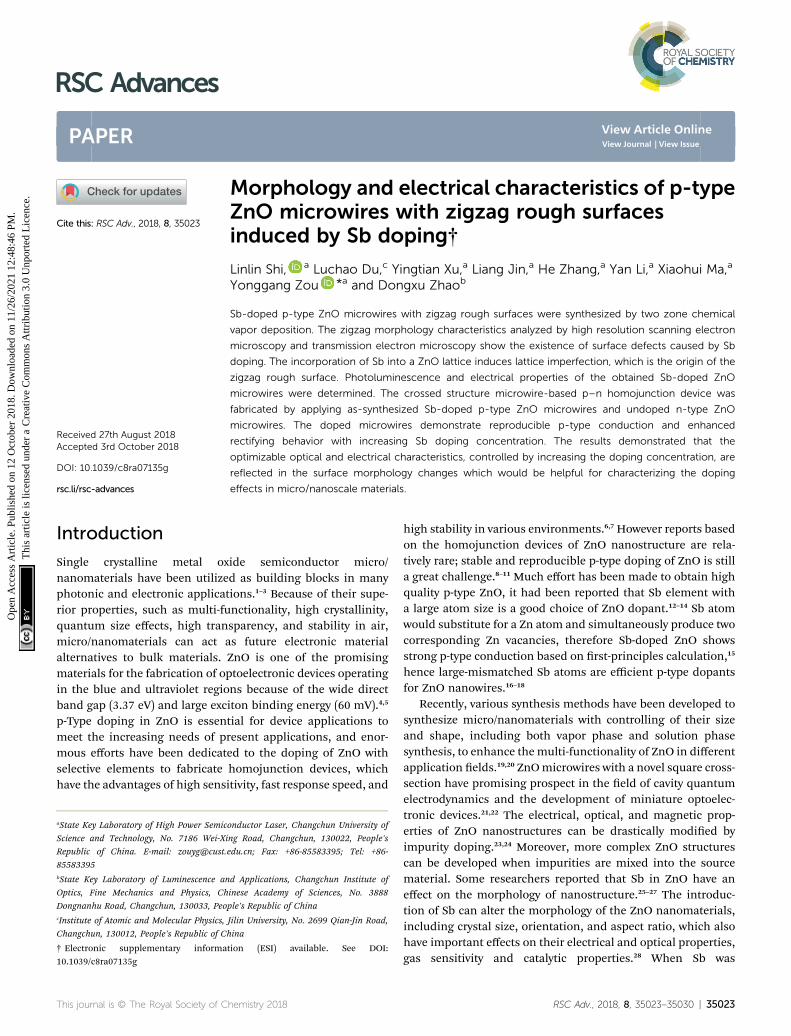
Fig. 1 SEM images of the (a) undoped ZnOmicrowire shows a smooth su3% Sb-doped ZnO microwire shows more obviously zigzag rough surfaOptical image of the as-synthesized ultralong Sb-doped ZnO microwimicrowires, (g–j) the elemental mappings of Zn, O, Sb of the cross sect
35024 | RSC Adv., 2018, 8, 35023–35030
Results and discussionMorphologies and characterization
The as-synthesized ZnO microwire was analysed by ScanningElectron Microscope (SEM) to demonstrate the structuralcharacters. The morphologies of both undoped and Sb-dopedultralong ZnO microwires with square cross-section arerevealed in Fig. 1a–c. The surface morphology changesdistinctly due to the incorporation of the Sb dopant, themicrowire presents a zigzag rough surface compared to thesmooth surface of the undoped ZnO microwire. Fig. 1d displaysoptical imaging of the as synthesized ultralong ZnO microwireson an alumina boat, the length can reach to about 10 milli-meters. To determine the composition of Sb in ZnOmicrowires,we performed the Energy Dispersive X-ray spectroscopy (EDX)composition analysis taken in various regions to investigate Sband Zn distribution. The morphology variation was investi-gated, it changes with the concentration of the Sb element inthe microwire, Sb concentration was 0.1% and 0.3% in Sb-doped microwires within the measurement limit of EDX. Thesurface of zigzag roughness increases with the doping concen-tration, the details are shown from the inset enlarged SEMimage in Fig. 1e and f. With the increase of doping
rface. (b) 1% Sb-doped ZnOmicrowire shows a zigzag rough surface. (c)ce. Inset: the enlarged SEM images of Sb-doped ZnO microwires. (d)res. (e and f) EDX element analysis of 0.1% and 0.3% Sb-doped ZnOion of a Sb-doped ZnO microwire.
This journal is © The Royal Society of Chemistry 2018

Fig. 2 (a and b) HRTEM image taken from the zigzag area of ZnOmicrowire shows high quality crystallite. (c) The corresponding SAEDpattern. (d and e) SEM images amplification of the edges of Sb-dopedZnO microwire.
Fig. 3 (a) Schematic diagram of the growth process of the Sb-dopedZnO microwire, (b) schematic diagram of the two zone growthcondition.
Paper RSC Advances
Ope
n A
cces
s A
rtic
le. P
ublis
hed
on 1
2 O
ctob
er 2
018.
Dow
nloa
ded
on 1
1/26
/202
1 12
:48:
46 P
M.
Thi
s ar
ticle
is li
cens
ed u
nder
a C
reat
ive
Com
mon
s A
ttrib
utio
n 3.
0 U
npor
ted
Lic
ence
.View Article Online
concentration, triangle embossment became intensively andobviously in 0.3% Sb-doped microwire. To further conrm theexistence of Sb-doping, the cross section element mappings ofindividual Sb-doped ZnO microwires using EDX are depicted inFig. 1g–j. Zn, O and Sb are homogeneously and uniformlydistributed in the microwires. The inset is the local magniedportion with the energy from about 4 keV to 6 keV, indicatingthe existence of Sb in the doped material.
To understand the origin of the novel zigzag surfaces in themicrowires, the corresponding magnication of triangle edgesof the Sb-doped ZnO microwire were further determined byhigh-resolution TEM and SEM analysis. The results are recor-ded in Fig. 2. Detailed information can be obtained from theclear lattice structure, indicate good crystal quality. The c-axisgrowth direction with d-spacing of 0.52 nm was indicated byadjacent lattice spacing, it can be indexed into [0001] growthorientation, which is the favoured growth direction of ZnOmicrowire. The angle measurement of edges with respect to the[002] direction revealed an angle of �60� between the twoplanar defects,25 which is consistent with the angle relationshipbetween the (010) and (002) planes in the SAED pattern.33 Thecorresponding selected area electron diffraction (SAED) patternin Fig. 2c reveals that the growth orientations is along [0001].The internal structures of the Sb-doped ZnO microwires werefurther characterized by enlarged SEM characterizations oftriangle zone of microwire surface which are shown in Fig. 2dand e. The enlarged images of the edges of ZnO microwiredisplay a smooth transition of the edges of ZnO displaya smooth transition between the zigzag surface and internalmicrowire, both in 0.1% Sb-doped (Fig. 2d) and 0.3% Sb-doped(Fig. 2e) microwire. The above results reveal that Sb-doped ZnOmicrowires were highly crystallized with zigzag surface.
The origination of the zigzag rough surface in ZnO micro-wires could be attributed to the introduction of Sb dopants. Sbelement is responsible for the formation of the single-side
This journal is © The Royal Society of Chemistry 2018
zigzag boundaries in the nanowires, the radius of Sb3+ (0.078nm) is much larger than that of Zn2+ (0.074 nm), the introduc-tion of Sb3+ ions should cause a large structural strain. Since theradius of Sb3+ (0.78 A) is much larger than that of Zn2+ (0.74 A),the introduction of Sb atoms would cause a large structuralstrain, the release of the structural strain could result in theformation of the planar defects.34 When Sb in ZnO, the surfaceenergy of (001) planes is reduced, crystal growth along the (001)orientation is suppressed, and then the morphology of the ZnOmicro/nanowires can be changed. ZnO microwires usually growalong the c axis, and the side surfaces are {0110} and/or {2110}because of the lower energy surfaces compared to (0001).25 Thesolutes prefer to segregate from the host and occupy the surfaceof the nanostructures, result in a decreased surface energy.26
Hence we propose that Sb is responsible for the zigzag surfaceand zigzag shaped microwires are surrounded by (0002), (0110)and (2110) as the surface.27
Growth mechanism
In our experiment, the doping procedure performed under thetwo zone in situ synthesis condition, the synthesis condition isshown in Fig. 3. The Sb source served as the dopant sourcematerial could vaporize at the same speed with Zn source. Whenthe substrate was heated to about 1100 �C, oxygen was intro-duced for about 2 min to keep the synthesis under the oxygen-rich conditions which would suppress the formation of SbO.The rough surface morphologies become obviously withincreasing the O2 ow, which is shown in Fig. S1.† Based on theabove experimental process and relevant analyses, we proposedthe growth mechanism of the doping procedure of in situdoping of Sb-doped ZnO microwire, the schematic diagram isshown in Fig. 3a. The reaction temperature of Sb source (Sb2O3
powder) is about 600 �C, which is much lower than the synthesistemperature of ZnO. By separating two heating zones, Zn and Sbvapor was generated simultaneously to the growth substrate
RSC Adv., 2018, 8, 35023–35030 | 35025

RSC Advances Paper
Ope
n A
cces
s A
rtic
le. P
ublis
hed
on 1
2 O
ctob
er 2
018.
Dow
nloa
ded
on 1
1/26
/202
1 12
:48:
46 P
M.
Thi
s ar
ticle
is li
cens
ed u
nder
a C
reat
ive
Com
mon
s A
ttrib
utio
n 3.
0 U
npor
ted
Lic
ence
.View Article Online
with the temperature increasing, deposited on the growthsubstrate to form droplets. As the O2 gas was introduced intothe furnace at 1100 �C, when the ZnO in the droplets reacha saturated concentration, Sb-doped crystalline ZnO begin togrow from the droplets. The initially formed Sb vapor from thesource can provide the necessary feeding dopant material forthe microwire growth. It suggests that Sb vapor is diffused fullof the whole growth process, the surface zigzag morphologyaffected by the inside defect could contribute to the introduc-tion of Sb atoms in the ZnO crystal growth process.24
Optical properties
To investigate optical properties of the ZnO microwires, pho-toluminescence (PL) spectra were measured at room tempera-ture using the 325 nm line of a He–Cd laser as an excitationsource, the results are shown in Fig. 4a. As can be seen from thePL spectra, the near-band edge (NBE) emission centered at382 nm can be mainly observed in both undoped and Sb-dopedZnO microwires, there are two emission peaks in Sb-doped ZnOmicrowires with an ultraviolet (UV) emission related to the NBE
Fig. 4 (a) Normalized photoluminescence of Sb-doped and undopedZnOmicrowires at room temperature, (b) Raman spectra of Sb-dopedand undoped ZnO microwires.
35026 | RSC Adv., 2018, 8, 35023–35030
attributed to the exciton recombination of ZnO, and a broadgreen emission band related to defects at centered at 500 nm inboth 0.1% and 0.3% Sb-doped microwires. The broad visibleemission can be identied as deep level defects which usuallycaused by impurities and structural defects.35 According to thenormalized PL spectrum in Fig. 4a, the intensity ratios of thevisible emission to the UV emission of 0.3% Sb-doped micro-wire is larger than 0.1% Sb-doped microwire, the increasingdefect emission peak could be result from the introducing ofincreased impurity atoms, indicates the decreased crystallinityof the zigzag ZnO nanostructure and effective Sb defects inside.Compared with the undoped ZnO microwire, the intrinsicemission of 0.3% doped microwire is at 377.37 nm (3.26 eV),with a marked deviation of 0.085 eV from the emission(387.65 nm, 3.19 eV) of undoped ZnO. For 0.1% Sb-dopedmicrowire (384.04 nm, 3.23 eV), the deviation is 0.04 eV,which is smaller than the 0.3% Sb-doped microwire. This isprobably due to the formation of acceptor levels by Sb doping.With the doping concentration increases, the intensity of defectemission peak increases and the zigzag rough surfaces becomeobvious.
The microstructure characterization and the optical propertyof the microwires were also investigated by the Raman scat-tering to further conrm the incorporation of Sb atoms into theZnO microwire lattices. As shown in Fig. 4b, the peak centeredat 436 cm�1 is usually attributed to the E2 modes of the undo-ped ZnO single crystal, and this peak shis toward lowerfrequency to 434 cm�1 when doping with Sb, which is caused bythe formation of the SbZn–2VZn low formation energy complexacceptor in Sb-doped ZnO microwires, the defect can be iden-tied as represented the shallow acceptor defect levels.34,36 Thepeak at 380 cm�1 corresponds to the A1T modes in ZnO isdepressed by Sb doping. Since the oxygen defect or the dopantatom directly affects the A1T modes, indicates that Sb dopantatoms would be responsible for the depression in 380 cm�1.37
Consequently, PL and Raman spectra characteristics reveal thatSb was incorporated into ZnO crystal lattices and the zigzagmorphology have an impact on the emission according to Sbdoping.
The p-type behaviour of the nanowires can also be conrmedoptically by low-temperature photoluminescence (PL). The low-temperature (at 85 K) PL spectra of Sb-doped ZnO microwireswere shown in Fig. 5a. The Sb-doped ZnO microwire spectrumshows a dominated emission peak centered at 3.354 eV, whichis associated with the neutral-acceptor-bound exciton (A0X)recombination.38 The emission peaks located at 3.296 eV and3.226 eV are ascribed to the free electron to acceptor (FA) anddonor–acceptor-pair (DAP) transitions, respectively.39 The PLanalysis suggests that the Sb-doped ZnO has shallow acceptorinduced energy levels, which result in the p-type behavior of themicrowires. The acceptor binding energy of EA in ZnO can beestimated by the following formula:
EA ¼ Egap � EFA þ kBT
2(1)
where EFA is a free electron to the FA, kB is the Boltzmanconstant, and T is the temperature. According to the equation,
This journal is © The Royal Society of Chemistry 2018
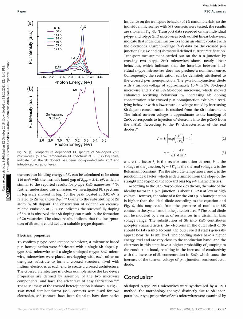
Fig. 5 (a) Temperature dependent PL spectra of Sb-doped ZnOmicrowires. (b) Low temperature PL spectrum at 85 K in log scale,indicate that the Sb dopant has been incorporated into ZnO andintroduced acceptor levels.
Paper RSC Advances
Ope
n A
cces
s A
rtic
le. P
ublis
hed
on 1
2 O
ctob
er 2
018.
Dow
nloa
ded
on 1
1/26
/202
1 12
:48:
46 P
M.
Thi
s ar
ticle
is li
cens
ed u
nder
a C
reat
ive
Com
mon
s A
ttrib
utio
n 3.
0 U
npor
ted
Lic
ence
.View Article Online
the acceptor binding energy of EA can be calculated to be about116 meV with the intrinsic band gap of Egap ¼ 3.41 eV, which issimilar to the reported results for p-type ZnO nanowires.13 Tofurther understand this emission, we investigated PL spectrumin log scale showed in Fig. 5b, the peak located at 3.02 eV isrelated to Zn vacancies (VZn).40 Owing to the substituting of Znatom by Sb dopant, the observation of evident Zn vacancy-related emission at 3.02 eV indicates the successfully dopingof Sb. It is observed that Sb doping can result in the formationof Zn vacancies. The above results indicate that the incorpora-tion of Sb atom could act as a suitable p-type dopant.
Electrical properties
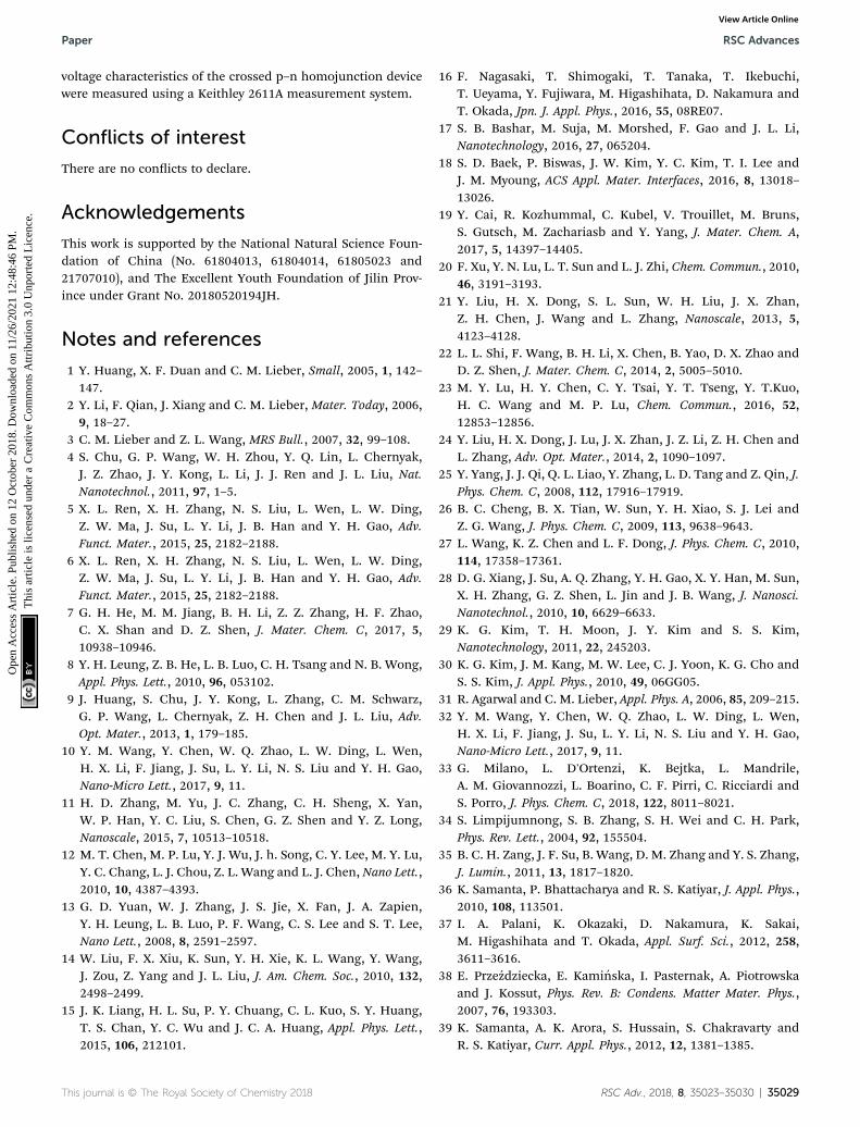
To conrm p-type conductance behaviour, a microwire-basedp–n homojunction were fabricated with a single Sb doped p-type ZnO microwire and a single undoped n-type ZnO micro-wire, microwires were placed overlapping with each other onthe glass substrate to form a crossed structure, xed withindium electrodes at each end to create a crossed architecture.The crossed architecture is a clear example since the key deviceproperties are dened by assembly of the two microwirecomponents, and have the advantage of easy fabrication.41,42
The SEM image of the crossed heterojunction is shown in Fig. 6.Two metal–semiconductor (MS) contacts were used for twoelectrodes, MS contacts have been found to have dominative
This journal is © The Royal Society of Chemistry 2018
inuence on the transport behavior of 1D nanomaterials, so theindividual microwires with MS contacts were tested, the resultsare shown in Fig. 6b. Transport data recorded on the individualp-type and n-type ZnOmicrowires both exhibit linear behaviors,indicate that individual microwires form an ohmic contact withthe electrodes. Current–voltage (I–V) data for the crossed p–njunction (Fig. 6c and d) shows well-dened current rectication.Transport measurement carried out on the n–n junction bycrossing two n-type ZnO microwires shows nearly linearbehaviour, which indicates that the interface between indi-vidual n-type microwires does not produce a nonlinear curve.Consequently, the rectication can be denitely attributed tothe crossed p–n homojunction. The p–n homojunction diodewith a turn-on voltage of approximately 10 V in 1% Sb-dopedmicrowire and 5 V in 3% Sb-doped microwire, which showedenhanced rectifying behaviour by increasing Sb dopingconcentration. The crossed p–n homojunction exhibits a recti-fying behavior with a lower turn-on voltage tuned by increasingSb dopant concentration is resulted from the Sb inducement.The initial turn-on voltage is approximate to the bandgap ofZnO, corresponds to injection of electrons into the p-ZnO fromthe n-ZnO. According to the IV characteristics of the realdiodes,43
I ¼ I0
�exp
�V
nVt
�� 1
�(2)
n ¼ q
kT
dV
d ln I(3)
where the factor I0 is the reverse saturation current, V is thevoltage at the junction, Vi ¼ kT/q is the thermal voltage, k is theBoltzmann constant, T is the absolute temperature, and n is thejunction ideal factor, which is determined from the slope of thestraight line region of the forward bias log I–V characteristics.
According to the Sah–Noyce–Shockley theory, the value of theideality factor in a p–n junction is about 1.0–2.0 at low or highvoltage. However, the value of n for the ZnO p–n homojunctionis higher than the ideal diode according to the equation andFig. 6, this may result from the presence of nonlinear MScontact in the system and in the junction area.44 The basal diodecan be modeled by a series of resistances in a dissimilar biasvoltage range. The substitution of Sb into ZnO contributesacceptor characteristics, the electrons in the outer shell of Sbshould be taken into account, the outer shell d states generallyappear near the Fermi level. The bonding states have a higherenergy level and are very close to the conduction band, and theelectrons in this state have a higher probability of jumping tothe conduction band, resulting in the increase of conductivitywith the increase of Sb concentration in ZnO, which cause theincrease of the turn-on voltage of p–n junction semiconductordiode.
Conclusion
Sb-doped p-type ZnO microwires were synthesized by a CVDmethod, the morphology changed distinctly due to Sb incor-poration. P-type properties of ZnOmicrowires were examined by
RSC Adv., 2018, 8, 35023–35030 | 35027

Fig. 6 (a) SEM image of microwire based crossed p–n homojunction. (b) I–V characteristics of individual n-type and p-type ZnOmicrowires andcrossed two single n-type ZnOmicrowires with n–n junction, (c and d) I–V characteristics of the crossed ZnOmicrowire p–n homojunction with0.1% Sb concentration (c) and 0.3% Sb concentration (d).
RSC Advances Paper
Ope
n A
cces
s A
rtic
le. P
ublis
hed
on 1
2 O
ctob
er 2
018.
Dow
nloa
ded
on 1
1/26
/202
1 12
:48:
46 P
M.
Thi
s ar
ticle
is li
cens
ed u
nder
a C
reat
ive
Com
mon
s A
ttrib
utio
n 3.
0 U
npor
ted
Lic
ence
.View Article Online
photoluminescence and electrical measurements. Low-temperature PL and Raman spectra measurements showedthat shallow acceptor was formed in the Sb-doped ZnO micro-wire. Fine rectication character was obtained on the crossedZnO microwire p–n homojunction indicating the p-typeconductivity of the Sb-doped ZnO microwire. The morphologyand electrical properties changes with Sb-doping. The dopedmicrowires demonstrate reproducible p-type conduction andenhanced rectifying behavior with increasing Sb dopingconcentration. The zigzag shape of ZnO microwires aerintroducing dopant could be a reection of effective doping, thecapability of testing p-type conduction characteristics and theunderstanding of emission behaviour of Sb-doped ZnO micro-wires have promising future applications of ZnO micro/nanowire based electronic and optoelectronic devices.
ExperimentalSynthesis of ZnO microwire
Sb-doped ZnO microwires were grown by a catalyst-free chem-ical vapor deposition (CVD) method with a two-zone tubefurnace. ZnO and graphite powders were thoroughly mixed witha weight ratio of 1 : 1, then the mixture was put into an aluminaboat to act as the reactant source material. The Sb2O3 powderswhich served as the dopant source material were loaded intoanother boat at the upstream to ensure that Sb2O3 and ZnOpowders could vaporize at the same speed. A 100 nm ZnO lm
35028 | RSC Adv., 2018, 8, 35023–35030
was deposited on the Si substrate by the sputtering method, andthen the substrate was loaded above the ZnO powders. Duringthe synthesis progress, the two sources were loaded into thefurnace at different temperature zones with a constant ow of100 sccm argon (99.99%) as the carrier gas. The reactant ZnOsource was heated to 1100 �C and the Sb2O3 dopant source washeated to 600 �C, simultaneously. When the ZnO source washeated to about 1100 �C, oxygen was introduced with a 20 sccmow rate for about 2 min to keep the synthesis under theoxygen-rich conditions which would suppress the formation ofVO and SbO. Aer maintaining the source temperature for40 min, the furnace was turned off and cooled down to roomtemperature. The synthesis of the undoped ZnO microwiresfollows the same procedure without the Sb dopant source.
Measurements
The morphology of the ZnO microwires was characterized bya eld-emission scanning electron microscope (FE-SEM)(model: Hitachi S-4800) equipped with an X-ray energy disper-sive spectrometer (EDX). The selected area electron diffraction(SAED) patterns were obtained on a JEOL JEM-2100F. Photo-luminescence (PL) measurement was carried out with a JY-630micro-Raman spectrometer employing the 325 nm line ofa He–Cd laser as the excitation source, and the room tempera-ture Raman spectra were recorded using the samemicro-Ramanspectrometer with a 488 nm excitation source. The current–
This journal is © The Royal Society of Chemistry 2018
Paper RSC Advances
Ope
n A
cces
s A
rtic
le. P
ublis
hed
on 1
2 O
ctob
er 2
018.
Dow
nloa
ded
on 1
1/26
/202
1 12
:48:
46 P
M.
Thi
s ar
ticle
is li
cens
ed u
nder
a C
reat
ive
Com
mon
s A
ttrib
utio
n 3.
0 U
npor
ted
Lic
ence
.View Article Online
voltage characteristics of the crossed p–n homojunction devicewere measured using a Keithley 2611A measurement system.
Conflicts of interest
There are no conicts to declare.
Acknowledgements
This work is supported by the National Natural Science Foun-dation of China (No. 61804013, 61804014, 61805023 and21707010), and The Excellent Youth Foundation of Jilin Prov-ince under Grant No. 20180520194JH.
Notes and references
1 Y. Huang, X. F. Duan and C. M. Lieber, Small, 2005, 1, 142–147.
2 Y. Li, F. Qian, J. Xiang and C. M. Lieber, Mater. Today, 2006,9, 18–27.
3 C. M. Lieber and Z. L. Wang, MRS Bull., 2007, 32, 99–108.4 S. Chu, G. P. Wang, W. H. Zhou, Y. Q. Lin, L. Chernyak,J. Z. Zhao, J. Y. Kong, L. Li, J. J. Ren and J. L. Liu, Nat.Nanotechnol., 2011, 97, 1–5.
5 X. L. Ren, X. H. Zhang, N. S. Liu, L. Wen, L. W. Ding,Z. W. Ma, J. Su, L. Y. Li, J. B. Han and Y. H. Gao, Adv.Funct. Mater., 2015, 25, 2182–2188.
6 X. L. Ren, X. H. Zhang, N. S. Liu, L. Wen, L. W. Ding,Z. W. Ma, J. Su, L. Y. Li, J. B. Han and Y. H. Gao, Adv.Funct. Mater., 2015, 25, 2182–2188.
7 G. H. He, M. M. Jiang, B. H. Li, Z. Z. Zhang, H. F. Zhao,C. X. Shan and D. Z. Shen, J. Mater. Chem. C, 2017, 5,10938–10946.
8 Y. H. Leung, Z. B. He, L. B. Luo, C. H. Tsang and N. B. Wong,Appl. Phys. Lett., 2010, 96, 053102.
9 J. Huang, S. Chu, J. Y. Kong, L. Zhang, C. M. Schwarz,G. P. Wang, L. Chernyak, Z. H. Chen and J. L. Liu, Adv.Opt. Mater., 2013, 1, 179–185.
10 Y. M. Wang, Y. Chen, W. Q. Zhao, L. W. Ding, L. Wen,H. X. Li, F. Jiang, J. Su, L. Y. Li, N. S. Liu and Y. H. Gao,Nano-Micro Lett., 2017, 9, 11.
11 H. D. Zhang, M. Yu, J. C. Zhang, C. H. Sheng, X. Yan,W. P. Han, Y. C. Liu, S. Chen, G. Z. Shen and Y. Z. Long,Nanoscale, 2015, 7, 10513–10518.
12 M. T. Chen, M. P. Lu, Y. J. Wu, J. h. Song, C. Y. Lee, M. Y. Lu,Y. C. Chang, L. J. Chou, Z. L. Wang and L. J. Chen, Nano Lett.,2010, 10, 4387–4393.
13 G. D. Yuan, W. J. Zhang, J. S. Jie, X. Fan, J. A. Zapien,Y. H. Leung, L. B. Luo, P. F. Wang, C. S. Lee and S. T. Lee,Nano Lett., 2008, 8, 2591–2597.
14 W. Liu, F. X. Xiu, K. Sun, Y. H. Xie, K. L. Wang, Y. Wang,J. Zou, Z. Yang and J. L. Liu, J. Am. Chem. Soc., 2010, 132,2498–2499.
15 J. K. Liang, H. L. Su, P. Y. Chuang, C. L. Kuo, S. Y. Huang,T. S. Chan, Y. C. Wu and J. C. A. Huang, Appl. Phys. Lett.,2015, 106, 212101.
This journal is © The Royal Society of Chemistry 2018
16 F. Nagasaki, T. Shimogaki, T. Tanaka, T. Ikebuchi,T. Ueyama, Y. Fujiwara, M. Higashihata, D. Nakamura andT. Okada, Jpn. J. Appl. Phys., 2016, 55, 08RE07.
17 S. B. Bashar, M. Suja, M. Morshed, F. Gao and J. L. Li,Nanotechnology, 2016, 27, 065204.
18 S. D. Baek, P. Biswas, J. W. Kim, Y. C. Kim, T. I. Lee andJ. M. Myoung, ACS Appl. Mater. Interfaces, 2016, 8, 13018–13026.
19 Y. Cai, R. Kozhummal, C. Kubel, V. Trouillet, M. Bruns,S. Gutsch, M. Zachariasb and Y. Yang, J. Mater. Chem. A,2017, 5, 14397–14405.
20 F. Xu, Y. N. Lu, L. T. Sun and L. J. Zhi, Chem. Commun., 2010,46, 3191–3193.
21 Y. Liu, H. X. Dong, S. L. Sun, W. H. Liu, J. X. Zhan,Z. H. Chen, J. Wang and L. Zhang, Nanoscale, 2013, 5,4123–4128.
22 L. L. Shi, F. Wang, B. H. Li, X. Chen, B. Yao, D. X. Zhao andD. Z. Shen, J. Mater. Chem. C, 2014, 2, 5005–5010.
23 M. Y. Lu, H. Y. Chen, C. Y. Tsai, Y. T. Tseng, Y. T.Kuo,H. C. Wang and M. P. Lu, Chem. Commun., 2016, 52,12853–12856.
24 Y. Liu, H. X. Dong, J. Lu, J. X. Zhan, J. Z. Li, Z. H. Chen andL. Zhang, Adv. Opt. Mater., 2014, 2, 1090–1097.
25 Y. Yang, J. J. Qi, Q. L. Liao, Y. Zhang, L. D. Tang and Z. Qin, J.Phys. Chem. C, 2008, 112, 17916–17919.
26 B. C. Cheng, B. X. Tian, W. Sun, Y. H. Xiao, S. J. Lei andZ. G. Wang, J. Phys. Chem. C, 2009, 113, 9638–9643.
27 L. Wang, K. Z. Chen and L. F. Dong, J. Phys. Chem. C, 2010,114, 17358–17361.
28 D. G. Xiang, J. Su, A. Q. Zhang, Y. H. Gao, X. Y. Han, M. Sun,X. H. Zhang, G. Z. Shen, L. Jin and J. B. Wang, J. Nanosci.Nanotechnol., 2010, 10, 6629–6633.
29 K. G. Kim, T. H. Moon, J. Y. Kim and S. S. Kim,Nanotechnology, 2011, 22, 245203.
30 K. G. Kim, J. M. Kang, M. W. Lee, C. J. Yoon, K. G. Cho andS. S. Kim, J. Appl. Phys., 2010, 49, 06GG05.
31 R. Agarwal and C. M. Lieber, Appl. Phys. A, 2006, 85, 209–215.32 Y. M. Wang, Y. Chen, W. Q. Zhao, L. W. Ding, L. Wen,
H. X. Li, F. Jiang, J. Su, L. Y. Li, N. S. Liu and Y. H. Gao,Nano-Micro Lett., 2017, 9, 11.
33 G. Milano, L. D'Ortenzi, K. Bejtka, L. Mandrile,A. M. Giovannozzi, L. Boarino, C. F. Pirri, C. Ricciardi andS. Porro, J. Phys. Chem. C, 2018, 122, 8011–8021.
34 S. Limpijumnong, S. B. Zhang, S. H. Wei and C. H. Park,Phys. Rev. Lett., 2004, 92, 155504.
35 B. C. H. Zang, J. F. Su, B. Wang, D. M. Zhang and Y. S. Zhang,J. Lumin., 2011, 13, 1817–1820.
36 K. Samanta, P. Bhattacharya and R. S. Katiyar, J. Appl. Phys.,2010, 108, 113501.
37 I. A. Palani, K. Okazaki, D. Nakamura, K. Sakai,M. Higashihata and T. Okada, Appl. Surf. Sci., 2012, 258,3611–3616.
38 E. Przezdziecka, E. Kaminska, I. Pasternak, A. Piotrowskaand J. Kossut, Phys. Rev. B: Condens. Matter Mater. Phys.,2007, 76, 193303.
39 K. Samanta, A. K. Arora, S. Hussain, S. Chakravarty andR. S. Katiyar, Curr. Appl. Phys., 2012, 12, 1381–1385.
RSC Adv., 2018, 8, 35023–35030 | 35029
RSC Advances Paper
Ope
n A
cces
s A
rtic
le. P
ublis
hed
on 1
2 O
ctob
er 2
018.
Dow
nloa
ded
on 1
1/26
/202
1 12
:48:
46 P
M.
Thi
s ar
ticle
is li
cens
ed u
nder
a C
reat
ive
Com
mon
s A
ttrib
utio
n 3.
0 U
npor
ted
Lic
ence
.View Article Online
40 F. X. Xiu, Z. Yang, L. J. Mandalapu, D. T. Zhao and J. L. Liu,Appl. Phys. Lett., 2005, 87, 252102.
41 M. Ding, Z. Guo, L. Q. Zhou, X. Fang, L. L. Zhang, L. Y. Zeng,L. N. Xie and H. B. Zhao, Crystals, 2018, 8, 223.
42 D. Panda and T. Y. Tseng, J. Mater. Sci., 2013, 48, 6849–6877.
35030 | RSC Adv., 2018, 8, 35023–35030
43 C. X. Wang, G. W. Yang, H. W. Liu, Y. H. Han, J. F. Luo,C. X. Gao and G. T. Zou, Appl. Phys. Lett., 2004, 84, 2427.
44 G. X. Zhu, Y. J. Liu, C. Zhang, Z. l. Zhu and Z. Xu, Chem. Lett.,2010, 39, 994–995.
This journal is © The Royal Society of Chemistry 2018