mos logic and gate circuits -...
TRANSCRIPT
MOS Logic and Gate Circuits
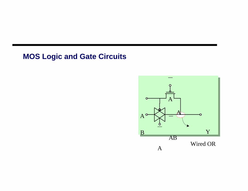
A
Y
A
BAB
A
A
Wired OR
IntroductionNMOS Logic
Resistive Load Saturated Enhancement LoadLinear Enhancement LoadDepletion LoadSome GatesTransient in NMOS CircuitPseudo-NMOS
CMOS LogicStatic CMOS Logic Gates
• NOT• NAND• NOR• Realization of More Complicated Gate CircuitsTransmission Gates Family
• NMOS Only Switch• CMOS
Differential Cascode Voltage Switch LogicRules of Thumb
Summary
Contents

The MOS inverter is the basic circuit exhibits all of the essential features of MOS Logic. Extension of MOS inverter concepts to NOR and NAND Gate is very simple. In this lecture we will analysis for VTC, NM, PD,… . Both NMOS and CMOS circuits are considered. Digital MOS circuits can be classified into two categories:
Static Circuits: require no clock or other periodic signal for operation. Clocks are required for static circuit in sequential logicDynamic Circuits: require periodic clock signals, synchronized with data signals, for proper operation even in combinational logic
Introduction

Vdd+
Vo
Vi
RL
Vo
VioOLV
Vdd
NMOS Logic
Resistive Load
W VoL C SpeedL
P RL Area
⎛ ⎞ ↑⇒ ↓⇒ ↑⇒ ↓⎜ ⎟⎝ ⎠↓⇒ ↑⇒ ↑
NMOS Logic
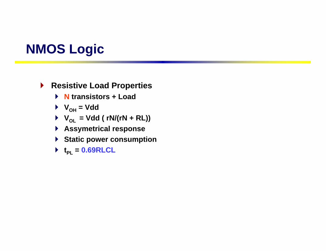
Resistive Load PropertiesN transistors + LoadVOH = VddVOL = Vdd ( rN/(rN + RL))Assymetrical responseStatic power consumptiontPL = 0.69RLCL
Vo
Vi
Vdd+ Vdd+
M2
M1Vo
VioOLV
OHV
Vo 1Vi
δ= −
δ
R∝ β
ILVIHV
NMOS Logic
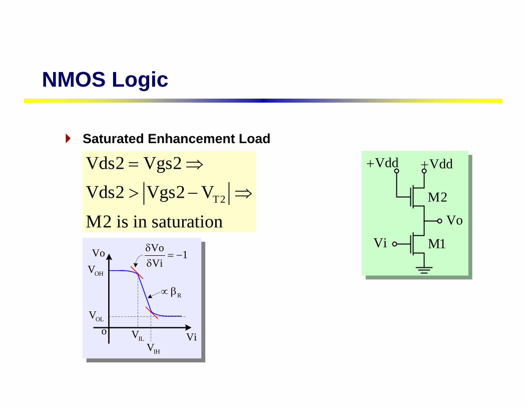
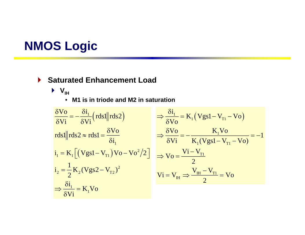
Saturated Enhancement Load
T2
Vds2 Vgs2Vds2 Vgs2 VM2 is in saturation
= ⇒
> − ⇒

Saturated Enhancement LoadVIL
IL T12 2
1 T1 2 T2
I 1
T
R
L
2
T
R
V V M1, M2 are in saturation
K (Vgs1 V ) K (Vgs2 V ) ,V CteVoVgs1 Vi, Vgs2 Vdd Vo , 1Vi
Vo 1Vi
V V
≥ ⇒
⇒ − = − ≈δ
= = − ⇒ = − β β >δ
δ⇒− ≈⇒ ≠
δ
NMOS Logic
Vo
VioOLV
OHV
Vo 1Vi
δ= −
δ
R∝ β
ILVIHV

Saturated Enhancement LoadVOL
• VOL is difficult to obtain because it is the output voltage when input equal to VOH, the resulting expression is a fourth order polynomial!
NMOS Logic
Vo
VioOLV
OHV
Vo 1Vi
δ= −
δ
R∝ β
ILVIHV
NMOS Logic
( )
( )
1
1
21 1 T1
22 2 T2
11
iVo rds1 rds2Vi Vi
Vords1 rds2 rds1i
i K Vgs1 V Vo Vo 2
1i K (Vgs2 V )2i
K VoVi
δδ= −
δ δδ
≈ =δ
⎡ ⎤= − −⎣ ⎦
= −
δ⇒ =
δ
Saturated Enhancement LoadVIH
• M1 is in triode and M2 in saturation
( )11 T1
1
1 T1
T1
IH T1IH
iK Vgs1 V Vo
VoK VoVo 1
Vi K (Vgs1 V Vo)Vi V
Vo2V V
Vi V Vo2
δ⇒ = − −
δδ
⇒ = − = −δ − −
−⇒ =
−= ⇒ =
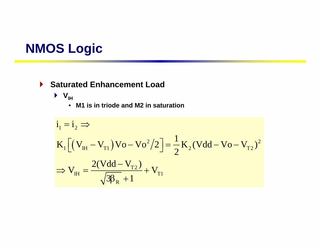
( )1 2
2 21 IH T1 2 T2
T2IH T1
R
i i1K V V Vo Vo 2 K (Vdd Vo V )2
2(Vdd V )V V
3 1
= ⇒
⎡ ⎤− − = − −⎣ ⎦
−⇒ = +
β +
NMOS Logic
Saturated Enhancement LoadVIH
• M1 is in triode and M2 in saturation
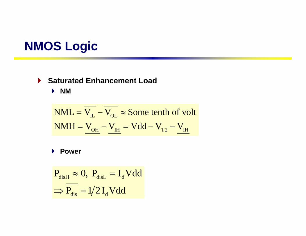
IL OL
OH IH T2 IH
NML V V Some tenth of voltNMH V V Vdd V V
= − ≈
= − = − −
NMOS Logic
Saturated Enhancement LoadNM
Power
disH disL d
dis d
P 0, P I Vdd
P 1 2I Vdd
≈ =
⇒ =
Vo
Vi
VGG
Vdd+
M2
M1
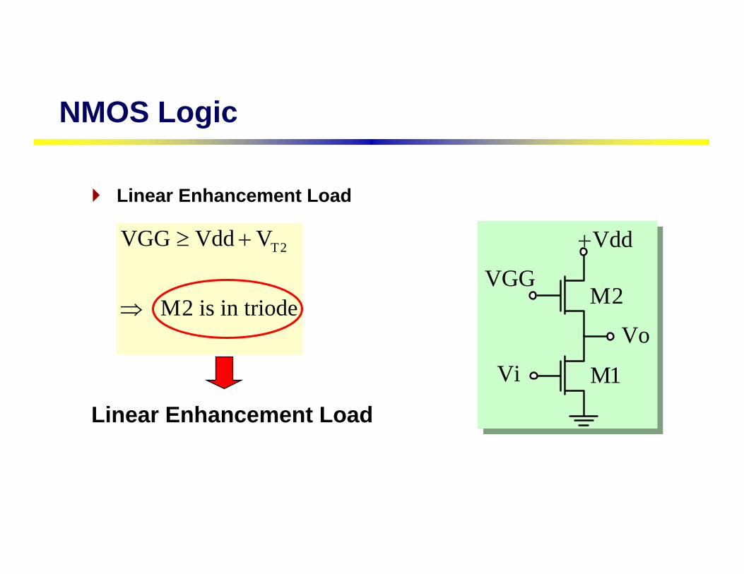
NMOS Logic
Linear Enhancement Load
Linear Enhancement Load
T2VGG Vdd V
M2 is in triode
≥ +
⇒

NMOS Logic
Vo
VioOLV
Vdd
ILVIHVTVVdd
Linear Enhancement LoadVTC
• By this circuit the VOHcan be increased (or Vddcan be decreased because Vomax = Vdd )

Linear Enhancement LoadVIL
• M1 is in saturation and M2 in triode
VIH • M1 and M2 are in triode
( )
( )
1 1
1
22 2 T2
22 T2
i iVo Vds2rds2Vi Vi Vi i
i K Vgs2 V Vds2 Vds2 2
iK VGG Vo V Vds2
Vds2
δ δδ δ= − = −
δ δ δ δ
⎡ ⎤= − −⎣ ⎦δ
= − − −δ
( )
21 1 T1
11 T1
1 T1
2 T2
IL
1i K (Vi V )2
iK Vi V
ViK (Vi V )Vo 1
Vi K (VGG Vo V Vds2)V f (Vo)
= −
δ= −
δ− −δ
= − =δ − − −⇒ =
NMOS Logic
rds2 rds1 rds2→
Rβ
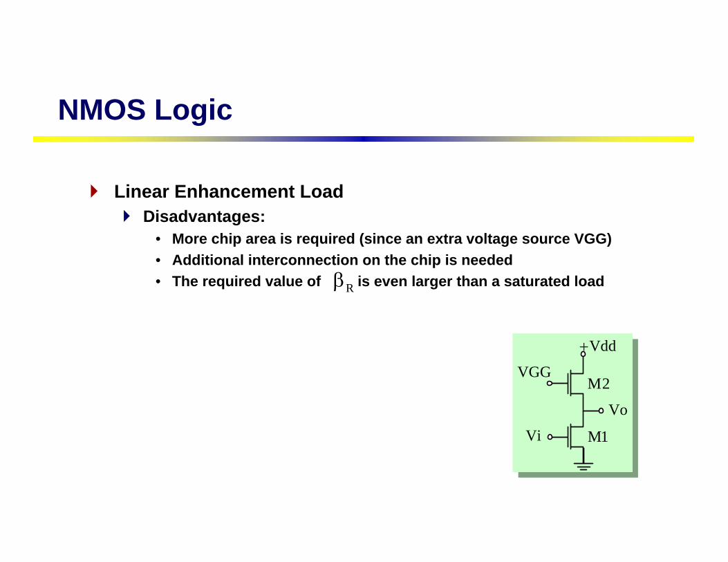
NMOS Logic
Linear Enhancement LoadDisadvantages:
• More chip area is required (since an extra voltage source VGG)• Additional interconnection on the chip is needed• The required value of is even larger than a saturated load
Vo
Vi
VGG
Vdd+
M2
M1

NMOS Logic
Depletion LoadIon implantation processing step is needed to create depletion device, but overcome the disadvantages of the previous circuit
Vo
Vi M1
Vdd+
M2

NMOS Logic
Depletion LoadVTC
Therefore M2 is in triode
1 1 2
222 T2 2
Vi Low i 0, M1 in cutoff i i 0K
if M2 is in saturation then i (Vgs2 V ) , Vgs2 0 i 02
= ⇒ = ⇒ = =
= − = ⇒ >
Vo
VioOLV
Vdd
ILVIHVTVVdd
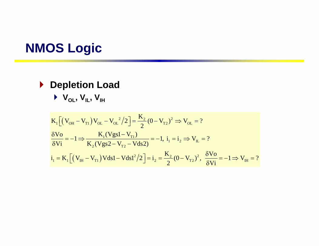
Depletion LoadVOL, VIL, VIH
NMOS Logic
( )
( )
2 221 OH T1 OL OL T2 OL
1 T11 2 IL
2 T2
2 221 1 IH T1 2 T2 IH
KK V V V V 2 (0 V ) V ?
2K (Vgs1 V )Vo 1 1, i i V ?
Vi K (Vgs2 V Vds2)K Voi K V V Vds1 Vds1 2 i (0 V ) , 1 V ?2 Vi
⎡ ⎤− − = − ⇒ =⎣ ⎦
−δ= − ⇒ = − = ⇒ =
δ − −
δ⎡ ⎤= − − = = − = − ⇒ =⎣ ⎦ δ
Some GatesIn all previous structures which different only in load, the following Gates can be implemented. Note that the NMOS Gates are not available as separately packaged individual circuits, but they are used extensively in LSI systems
• NOR Gates• NAND Gates
NMOS Logic
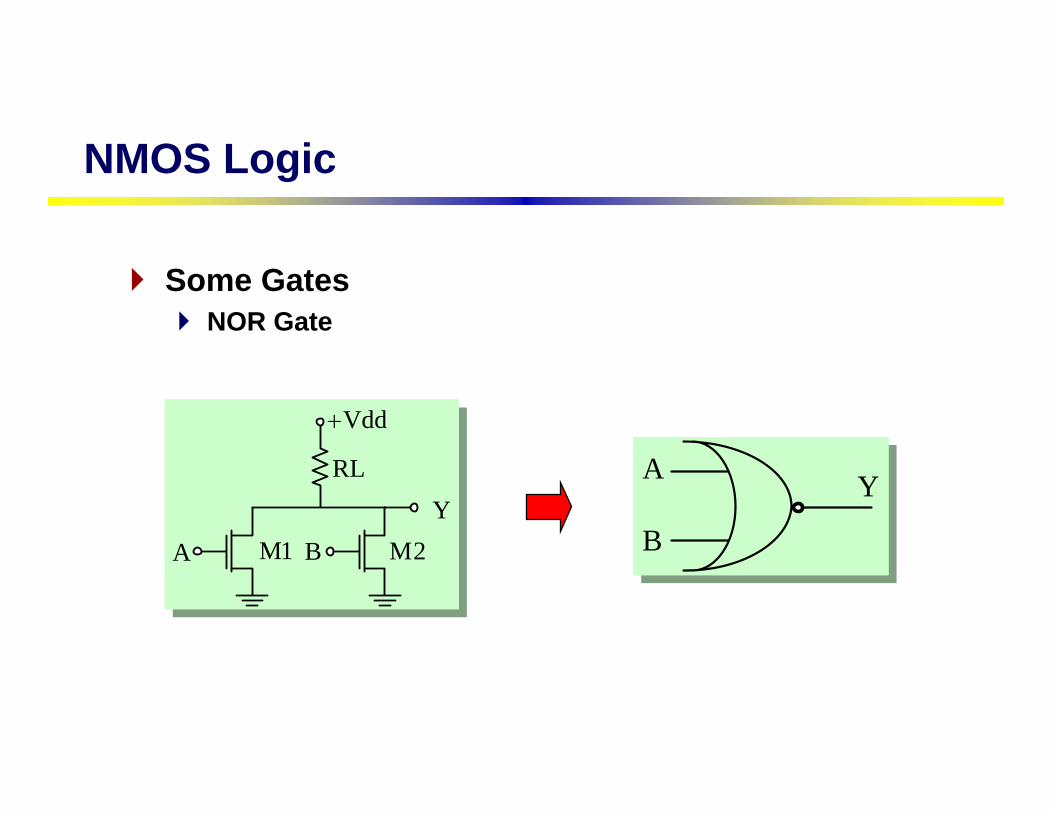
Some GatesNOR Gate
NMOS Logic
A M1Y
B M2
Vdd+
RL YA
B
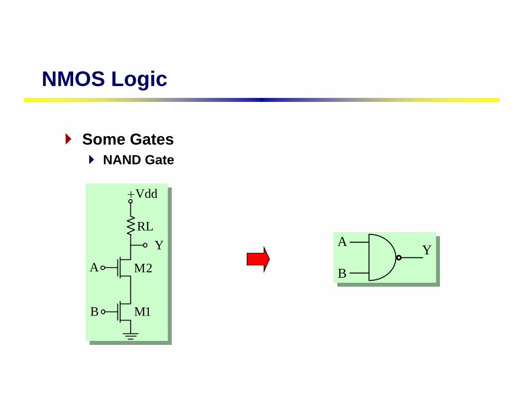
Some GatesNAND Gate
NMOS Logic
B
A
Vdd+
M2
M1
YRL
A
B
Y

Some GatesIn NOR Gate two transistors are paralleled but in NAND Gate two transistors are in series. Because of the need for increased area when adding NAND inputs, NAND logic with more than 2 inputs is not economically be attractive in NMOS. NOR logic is preferableIn NAND the M2 has body effectIn NOR we need the less interconnection (this can be shown from layout)
NMOS Logic
NMOS Logic
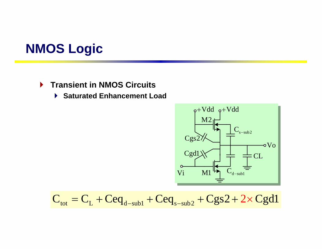
Transient in NMOS CircuitsSaturated Enhancement Load
tot L d sub1 s sub2C C Ceq Ceq Cgs2 Cgd2 1− −= + + + + ×
Vdd+Vdd+
M1
M2
Vi
Cgs2
Cgd1
s sub2C −
d sub1C −
CLVo
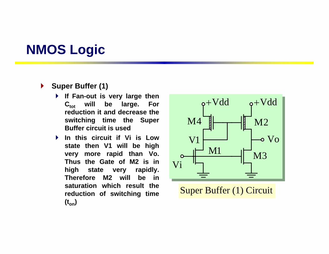
Super Buffer (1)If Fan-out is very large then Ctot will be large. For reduction it and decrease the switching time the Super Buffer circuit is usedIn this circuit if Vi is Low state then V1 will be high very more rapid than Vo. Thus the Gate of M2 is in high state very rapidly. Therefore M2 will be in saturation which result the reduction of switching time (ton)
M1
Vdd+
M4
Vo
M3
Vdd+
M2
Vi
V1
NMOS Logic
Super Buffer (1) Circuit
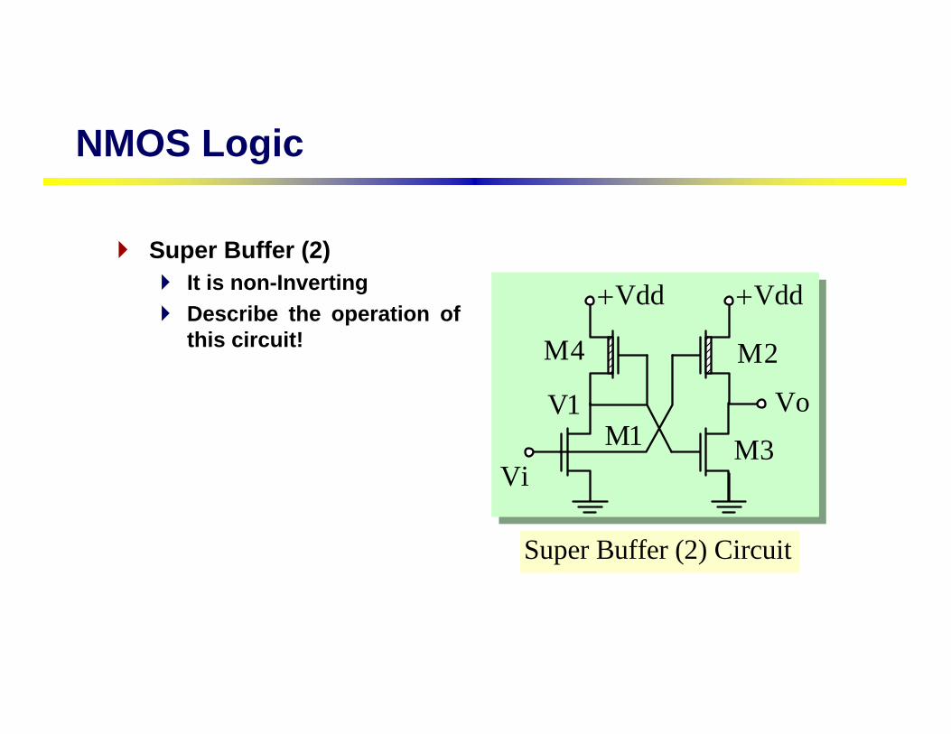
Super Buffer (2)It is non-InvertingDescribe the operation of this circuit!
NMOS Logic
Super Buffer (2) Circuit
M1
Vdd+
M4
Vo
M3
Vdd+
M2
Vi
V1

Pseudo-NMOSWhat makes a circuit fast?• I = C dV/dt -> tpd ∝ (C/I) DV• low capacitance• high current• small swing
Logical effort is proportional to C/IPMOS are the enemy!• High capacitance for a given current
Can we take the PMOS capacitance off the input?Various circuit families try to do this…
NMOS Logic

Pseudo-NMOSIn the old days, NMOS processes had no PMOS• Instead, use pull-up transistor that is always ON
In CMOS, use a PMOS that is always ON• Make PMOS about ¼ effective strength of pulldown
network
NMOS Logic
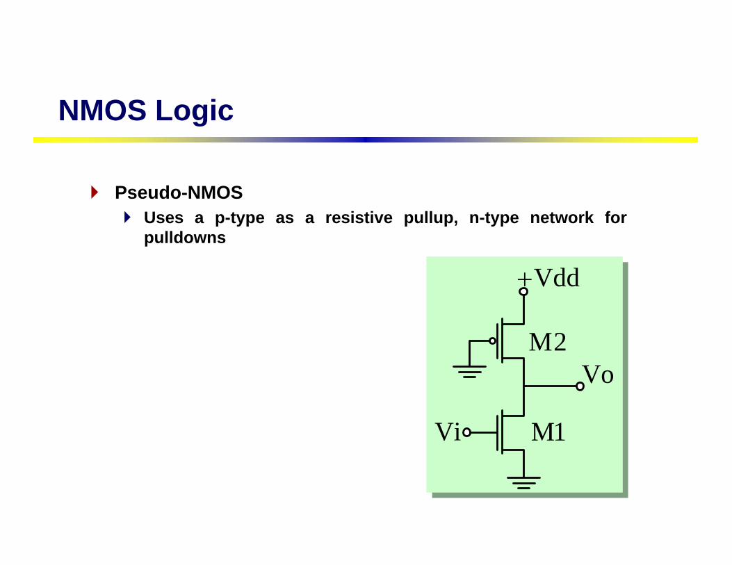
Pseudo-NMOSUses a p-type as a resistive pullup, n-type network for pulldowns
NMOS Logic
Vi M1
Vdd+
VoM2
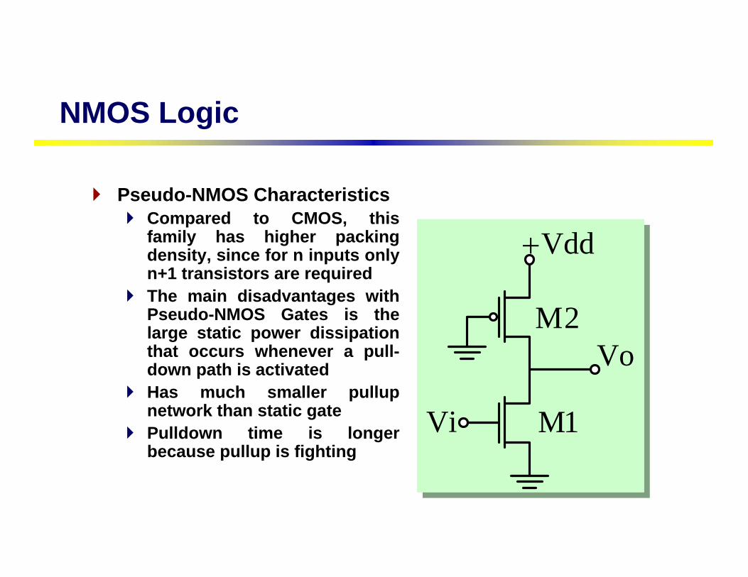
Pseudo-NMOS CharacteristicsCompared to CMOS, this family has higher packing density, since for n inputs only n+1 transistors are requiredThe main disadvantages with Pseudo-NMOS Gates is the large static power dissipation that occurs whenever a pull-down path is activated Has much smaller pullupnetwork than static gatePulldown time is longer because pullup is fighting
NMOS Logic
Vi M1
Vdd+
VoM2
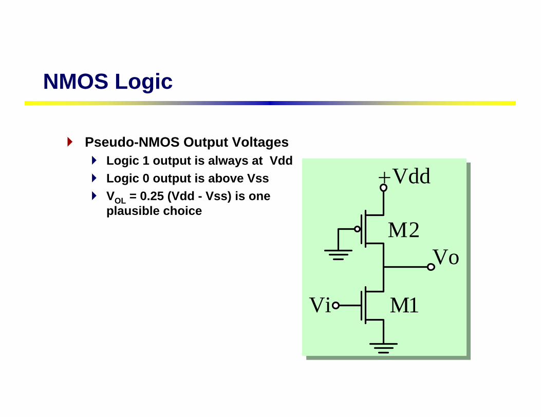
Pseudo-NMOS Output VoltagesLogic 1 output is always at VddLogic 0 output is above VssVOL = 0.25 (Vdd - Vss) is one plausible choice
Vi M1
Vdd+
VoM2
NMOS Logic
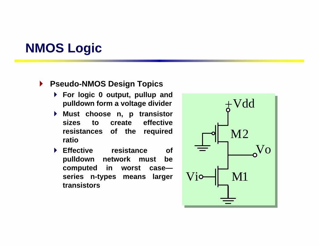
Pseudo-NMOS Design TopicsFor logic 0 output, pullup and pulldown form a voltage dividerMust choose n, p transistor sizes to create effective resistances of the required ratioEffective resistance of pulldown network must be computed in worst case—series n-types means larger transistors
Vi M1
Vdd+
VoM2
NMOS Logic
NMOS Logic
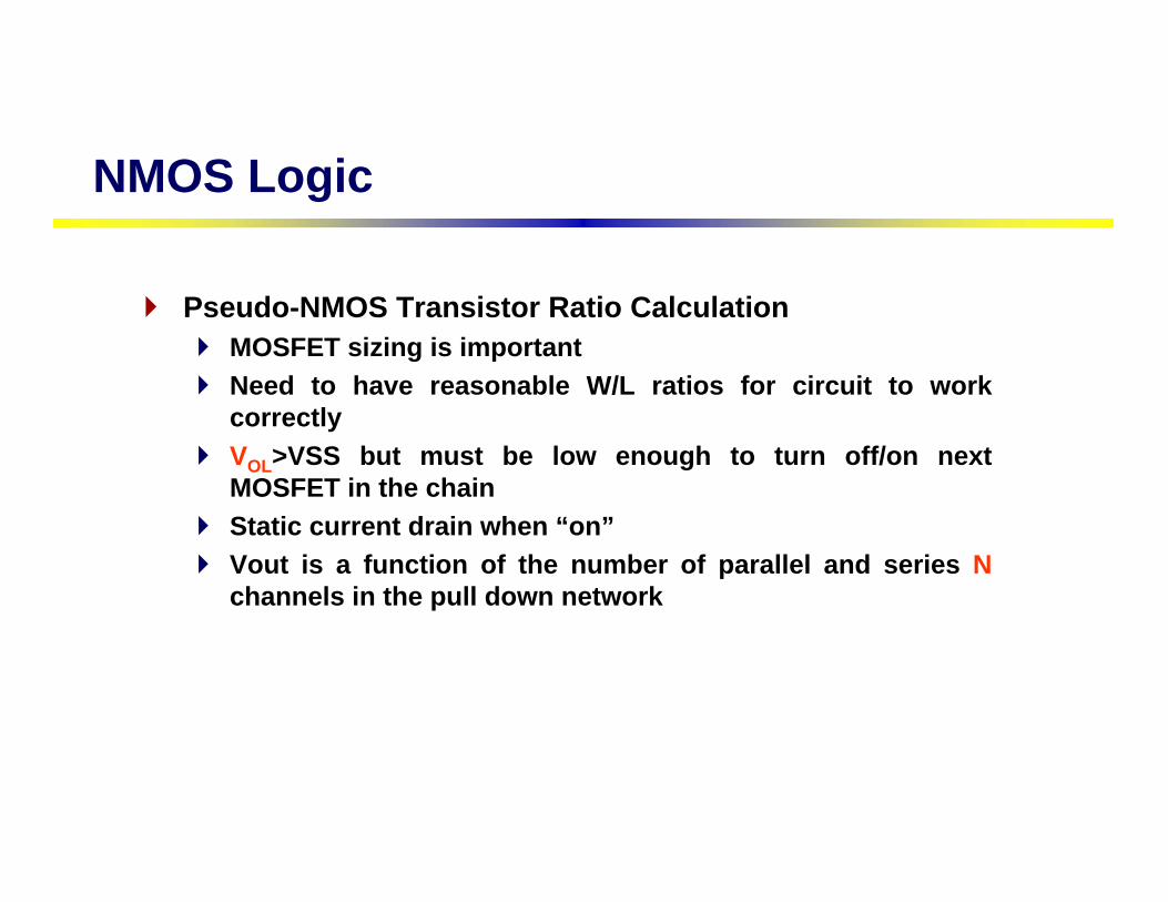
Pseudo-NMOS Transistor Ratio CalculationMOSFET sizing is importantNeed to have reasonable W/L ratios for circuit to work correctlyVOL>VSS but must be low enough to turn off/on next MOSFET in the chainStatic current drain when “on”Vout is a function of the number of parallel and series Nchannels in the pull down network
NMOS Logic
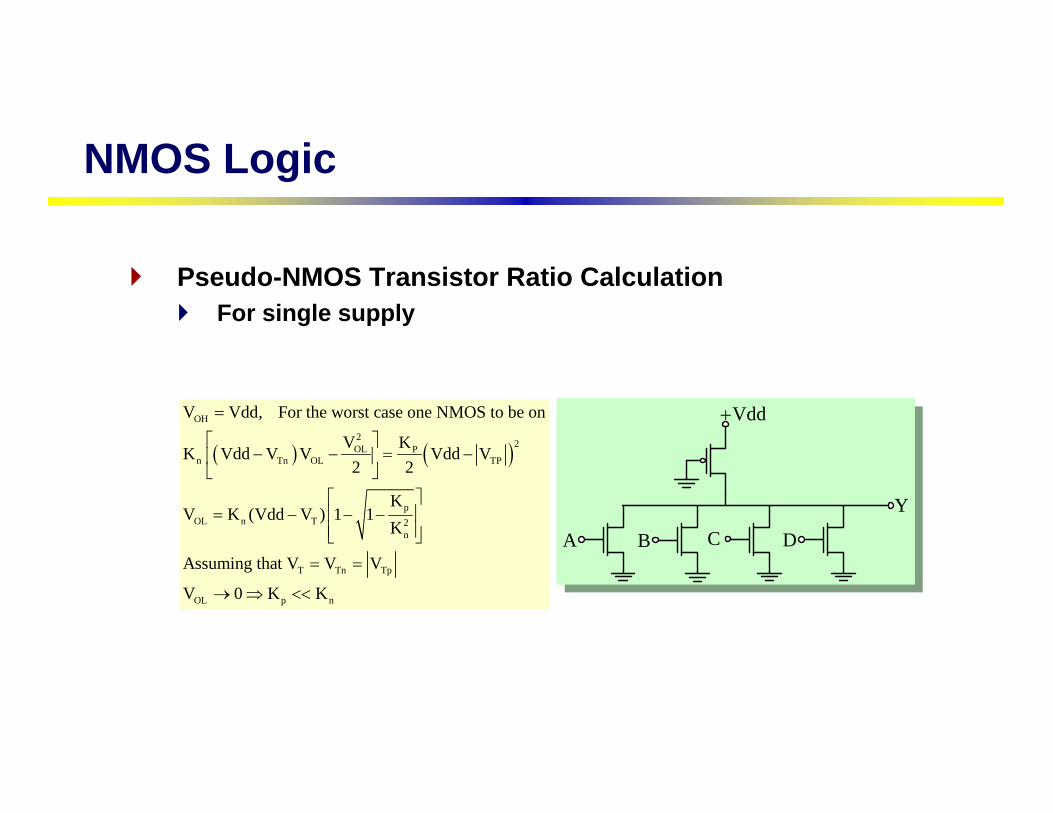
Pseudo-NMOS Transistor Ratio CalculationFor single supply
( ) ( )OH
22OL P
n Tn OL TP
pOL n T 2
n
T Tn Tp
OL p n
V Vdd, For the worst case one NMOS to be on
V KK Vdd V V Vdd V
2 2
KV K (Vdd V ) 1 1
K
Assuming that V V V
V 0 K K
=
⎡ ⎤− − = −⎢ ⎥
⎣ ⎦⎡ ⎤
= − − −⎢ ⎥⎢ ⎥⎣ ⎦
= =
→ ⇒ <<
A B C D
Vdd+
Y

0.0 0.5 1.0 1.5 2.0 2.50.0
0.5
1.0
1.5
2.0
2.5
3.0
Vin [V]
Vou
t[V
]
W/Lp = 4
W/Lp = 2
W/Lp = 1
W/Lp = 0.25
W/Lp = 0.5
NMOS Logic
Pseudo-NMOS VTC ( W/Ln=1)
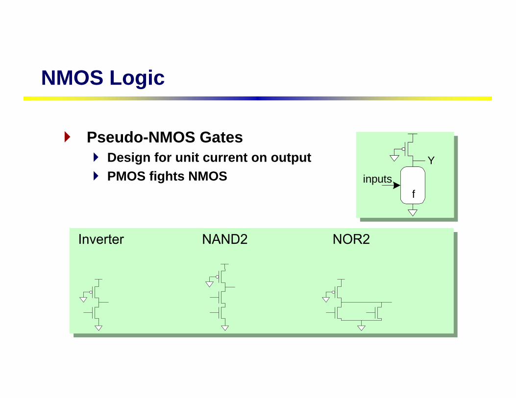
Pseudo-NMOS GatesDesign for unit current on outputPMOS fights NMOS
finputs
Y
NMOS Logic

Pseudo-NMOS PowerPseudo-NMOS draws power whenever Y = 0• Called static power P = I•VDD• A few mA / gate * 1M gates would be a problem• This is why NMOS went extinct!
Use Pseudo-NMOS sparingly for wide NORsTurn off PMOS when not in use
A BY
C
en
NMOS Logic
Out
In1 In2 In3 In4
NMOS Logic
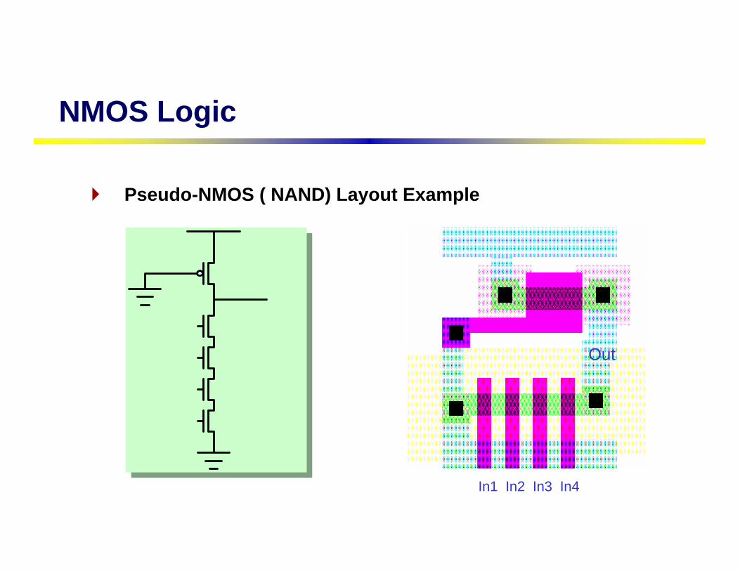
Pseudo-NMOS ( NAND) Layout Example

Static CMOS Logic FamilyAll of the circuits described in the previous sections have a large static power dissipation. This disadvantage can be overcome by using Static CMOS Logic Family
CMOS Logic
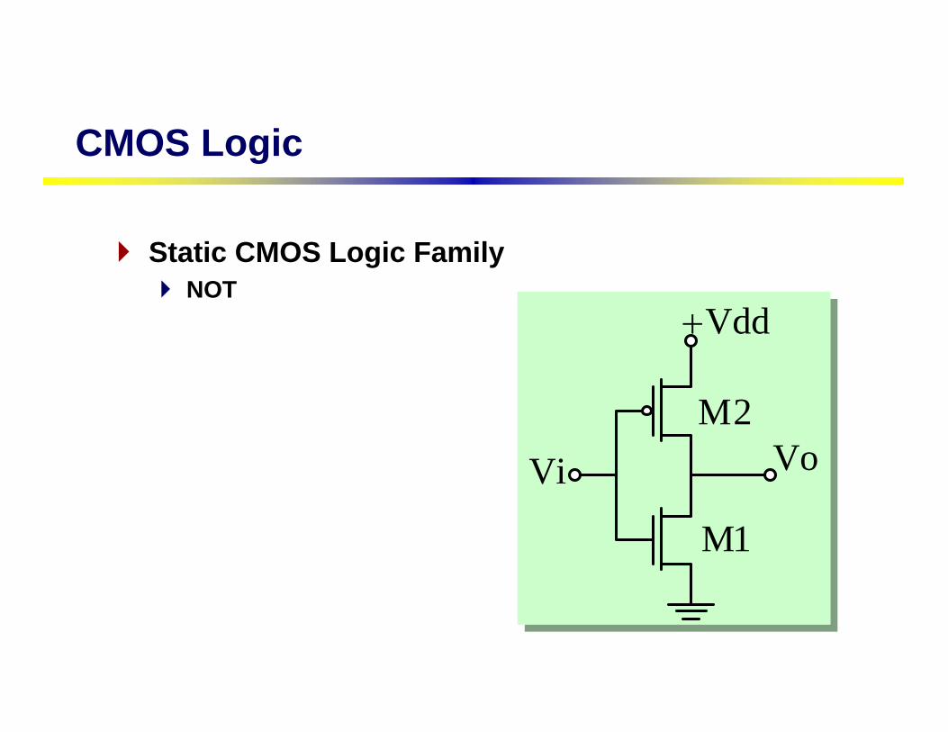
Vi
M1
Vdd+
VoM2
CMOS Logic
Static CMOS Logic FamilyNOT
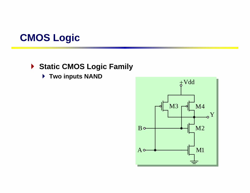
CMOS Logic
Static CMOS Logic FamilyTwo inputs NAND
M3
B M2
YM4
Vdd+
A M1

CMOS Logic
Static CMOS Logic FamilyTwo inputs NOR
Y
A
B
Vdd+
CMOS Logic
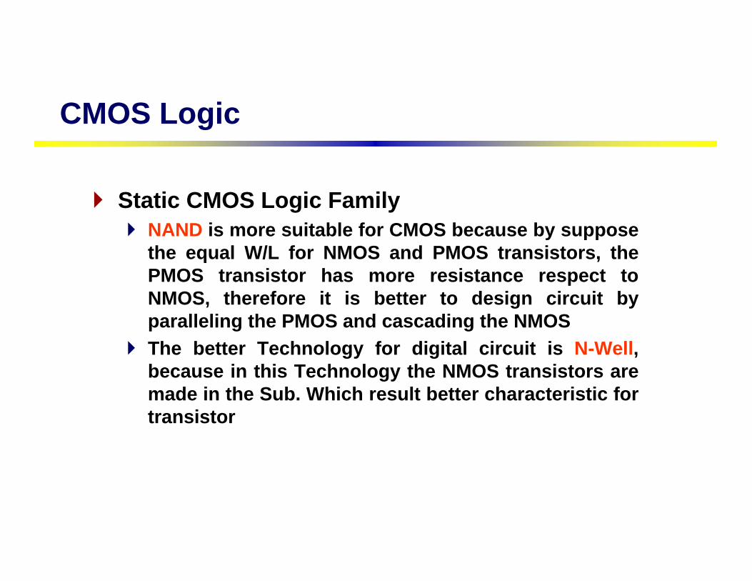
Static CMOS Logic FamilyNAND is more suitable for CMOS because by suppose the equal W/L for NMOS and PMOS transistors, the PMOS transistor has more resistance respect to NMOS, therefore it is better to design circuit by paralleling the PMOS and cascading the NMOSThe better Technology for digital circuit is N-Well, because in this Technology the NMOS transistors are made in the Sub. Which result better characteristic for transistor

Realization of More Complicated Gate Circuitsa) Y = A(B+C)It can be implemented in three levels:
• Gate Level• Transistor Level• Layout Level
CMOS Logic
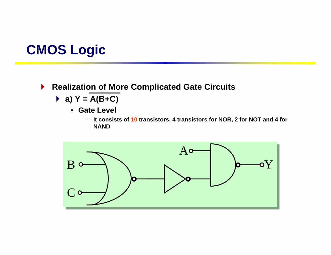
Realization of More Complicated Gate Circuitsa) Y = A(B+C)
• Gate Level– It consists of 10 transistors, 4 transistors for NOR, 2 for NOT and 4 for
NAND
AYB
C
CMOS Logic
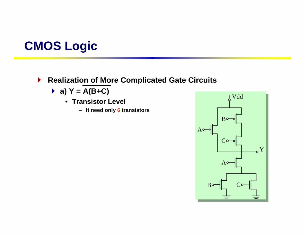
Realization of More Complicated Gate Circuitsa) Y = A(B+C)
• Transistor Level– It need only 6 transistors
A
B
C
Vdd+
Y
A
B C
CMOS Logic

Realization of More Complicated Gate Circuitsa) Y = A(B+C)
• Layout Level– By proper construction of layout, the parasitic capacitors are also
reduced and area can be saved
CMOS Logic
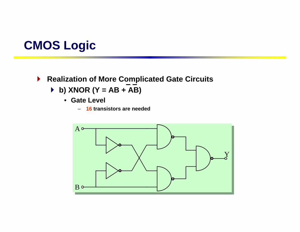
Realization of More Complicated Gate Circuitsb) XNOR (Y = AB + AB)
• Gate Level– 16 transistors are needed
A
B
Y
CMOS Logic
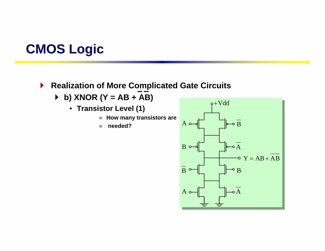
Realization of More Complicated Gate Circuitsb) XNOR (Y = AB + AB)
• Transistor Level (1)» How many transistors are» needed?
Vdd+
A
A
A
A
B
BB
B
Y AB AB= +
CMOS Logic
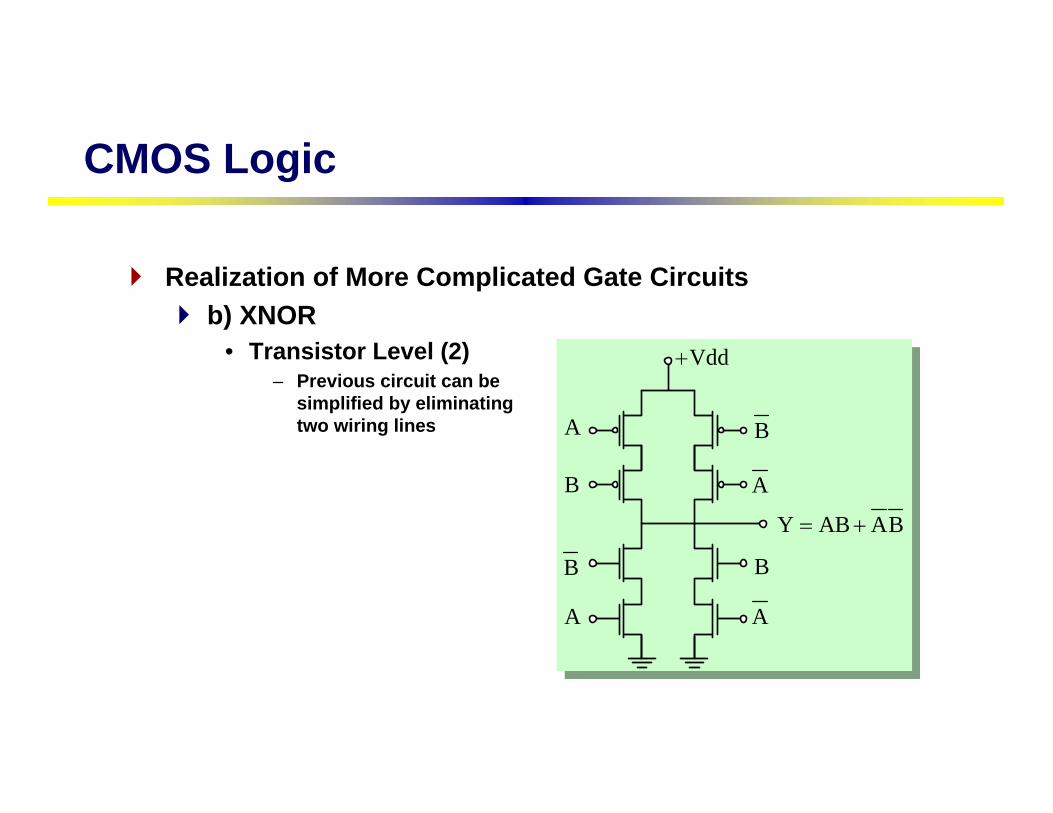
Realization of More Complicated Gate Circuitsb) XNOR
• Transistor Level (2)– Previous circuit can be
simplified by eliminatingtwo wiring lines
Vdd+
A
A
A
A
B
BB
B
Y AB AB= +
CMOS Logic

Realization of More Complicated Gate Circuitsb) XNOR
• Transistor Level (3)– In this circuit we have
static power dissipationin the state of (A=0,B=1)or (A=1,B=0)
A
M1
Vdd+
M3Y AB AB= +
M2
B
CMOS Logic
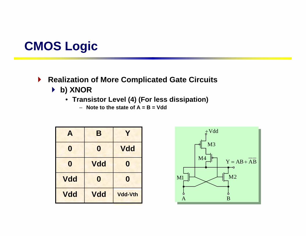
Realization of More Complicated Gate Circuitsb) XNOR
• Transistor Level (4) (For less dissipation)– Note to the state of A = B = Vdd
A
M1
Vdd+
M3
Y AB AB= +
M2
B
M4
Vdd-VthVddVdd
00Vdd
0Vdd0
Vdd00
YBA
CMOS Logic
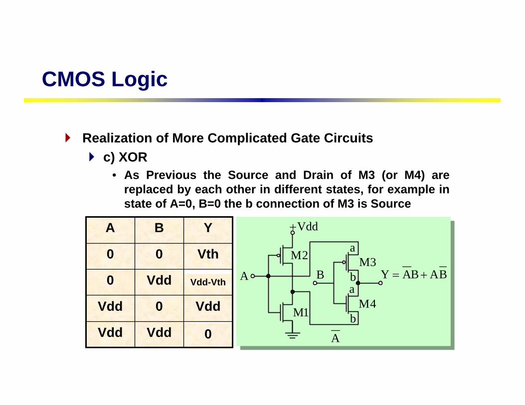
Realization of More Complicated Gate Circuitsc) XOR
• As Previous the Source and Drain of M3 (or M4) are replaced by each other in different states, for example in state of A=0, B=0 the b connection of M3 is Source
0VddVdd
Vdd0Vdd
Vdd-VthVdd0
Vth00
YBA Vdd+
A B
M1
M2 M3
M4
Y AB AB= +
A
a
ab
b
CMOS Logic

Realization of More Complicated Gate Circuitsd) Tri-State Outputs
• A floating state at the output is needed– Non-Inverting
D
En
Y
D
Vdd+En
Y
En 1 Y DEn 0 Y Hi Z
= ⇒ =⎧⎨ = ⇒ = −⎩
CMOS Logic
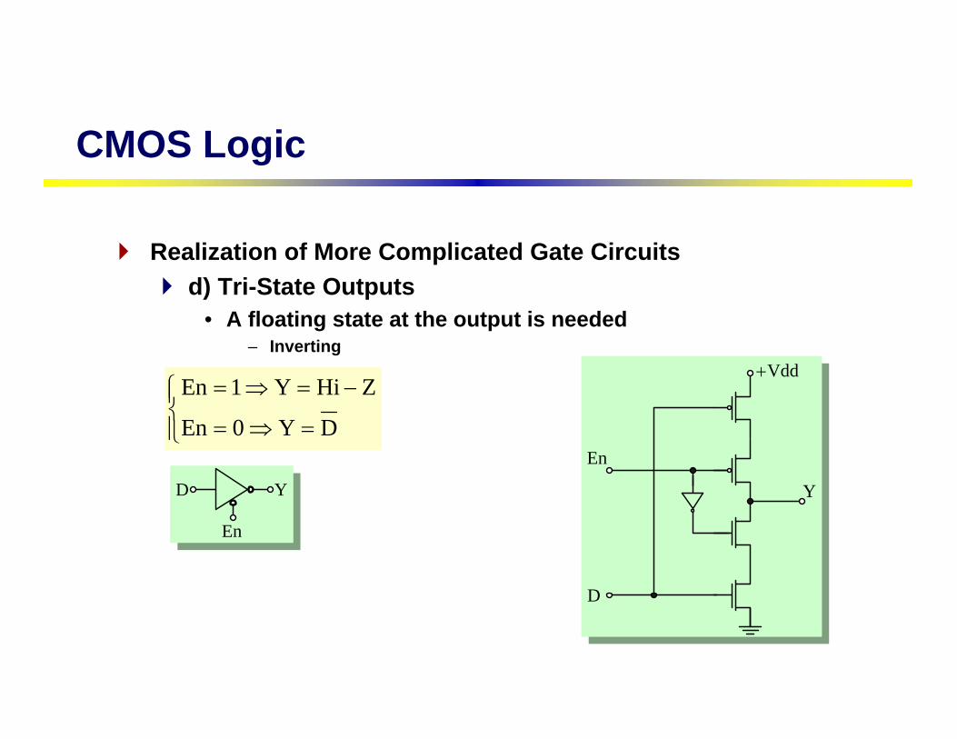
Realization of More Complicated Gate Circuitsd) Tri-State Outputs
• A floating state at the output is needed– Inverting
En 1 Y Hi Z
En 0 Y D
= ⇒ = −⎧⎪⎨
= ⇒ =⎪⎩
D
En
Y
Vdd+
D
En
Y
CMOS Logic
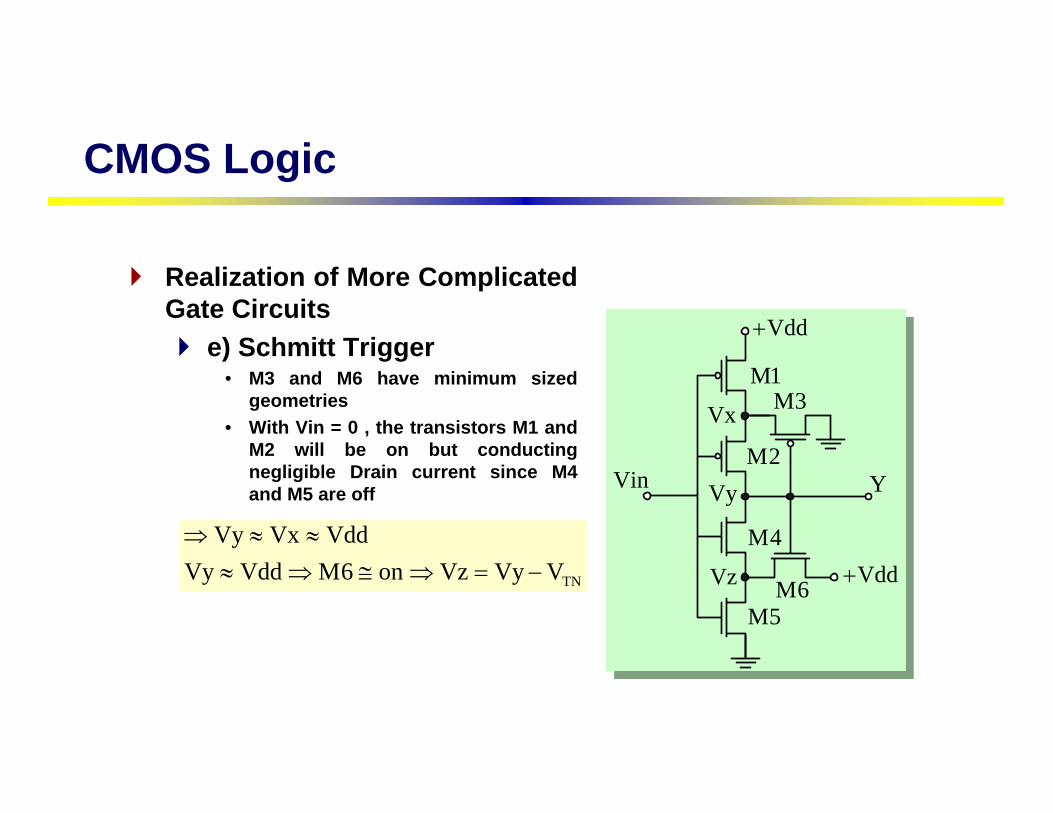
Realization of More Complicated Gate Circuits
e) Schmitt Trigger• M3 and M6 have minimum sized
geometries• With Vin = 0 , the transistors M1 and
M2 will be on but conducting negligible Drain current since M4 and M5 are off
Vdd+
Vin Y
Vdd+
M5M6Vz
M4
VyM2
M3M1
Vx
TN
Vy Vx VddVy Vdd M6 on Vz Vy V⇒ ≈ ≈
≈ ⇒ ≅ ⇒ = −
CMOS Logic
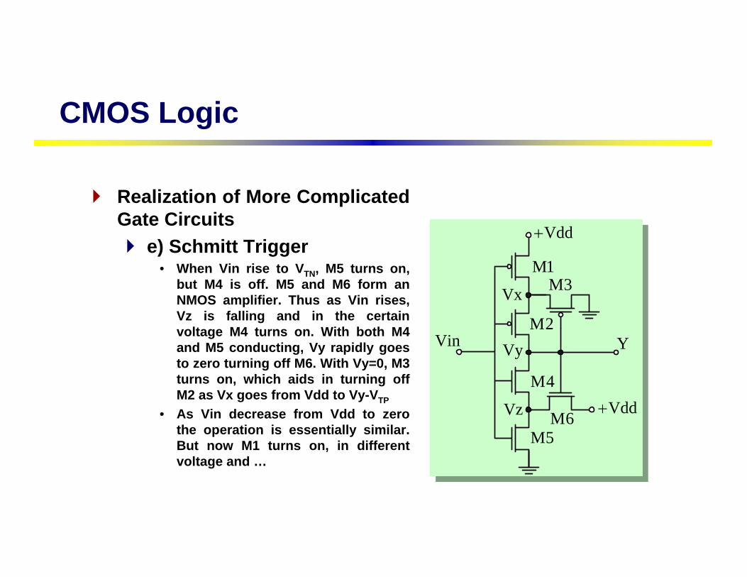
Realization of More Complicated Gate Circuits
e) Schmitt Trigger• When Vin rise to VTN, M5 turns on,
but M4 is off. M5 and M6 form an NMOS amplifier. Thus as Vin rises, Vz is falling and in the certain voltage M4 turns on. With both M4 and M5 conducting, Vy rapidly goes to zero turning off M6. With Vy=0, M3 turns on, which aids in turning off M2 as Vx goes from Vdd to Vy-VTP
• As Vin decrease from Vdd to zero the operation is essentially similar. But now M1 turns on, in different voltage and …
Vdd+
Vin Y
Vdd+
M5M6Vz
M4
VyM2
M3M1
Vx
CMOS Logic
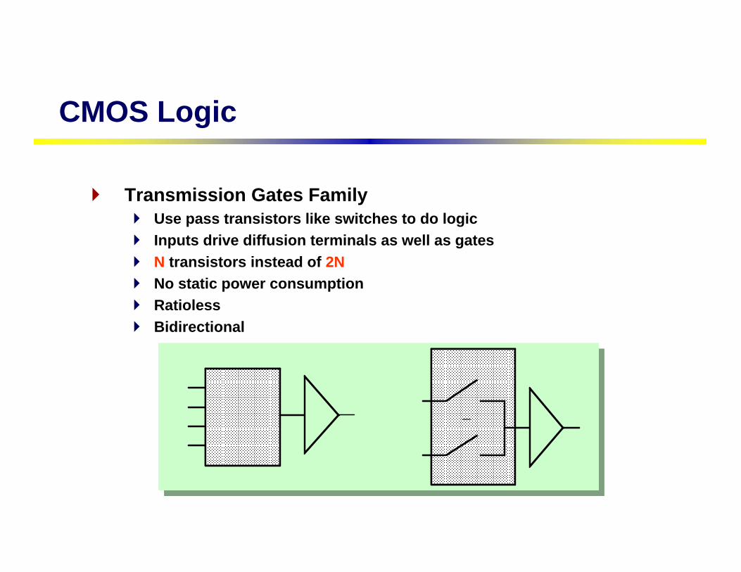
Transmission Gates FamilyUse pass transistors like switches to do logicInputs drive diffusion terminals as well as gatesN transistors instead of 2NNo static power consumptionRatiolessBidirectional
CMOS Logic
Transmission Gates FamilyNMOS Only Switch
CMOS Logic
0 0.5 1 1.5 20.0
1.0
2.0
3.0
Time [ns]
Volta
g e[V
]x
Out
In
Vdd X
In

Transmission Gates FamilyNMOS Only Switch• VB does not pull up to 2.5V, but 2.5-VTN
• Threshold voltage loss causes (M2 may be weakly conducting forming a path from Vdd to GND)
• NMOS has higher threshold than PMOS (body effect)
CMOS Logic

CMOS Logic
Transmission Gates FamilyNMOS Only Switch• Pass transistor gates should never be cascaded as on
the left• Logic on the right suffers from static power dissipation
and reduced noise margins
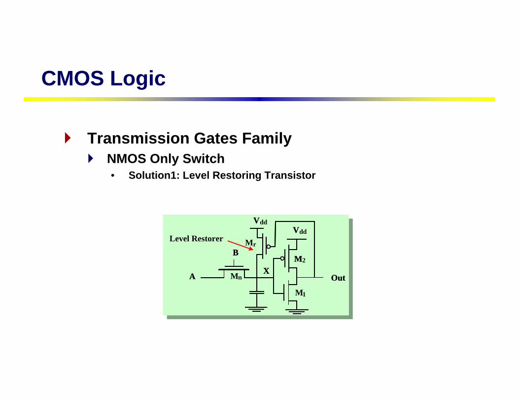
Transmission Gates FamilyNMOS Only Switch• Solution1: Level Restoring Transistor
CMOS Logic
M2
M1
n OutA
B
VVdd
XM
M
Mr
OutA
B
VddV
Level Restorer
X

Transmission Gates FamilyNMOS Only Switch• Solution1: Level Restoring Transistor
Advantages• Full swing on x (due to Level Restorer) so no static power
consumption by inverter• No static backward current path through Level Restorer and PT
since Restorer is only active when A is high• Restorer adds capacitance, takes away pull down current at X
For correct operation Mr must be sized correctly (ratioed)
CMOS Logic

Transmission Gates FamilyNMOS Only Switch• Solution2: Multiple VT Transistors
CMOS Logic
Out
In2 = 0V
In1 = 2.5V
A = 2.5V
B = 0V
low VT transistors
sneak path
on
off but leaking
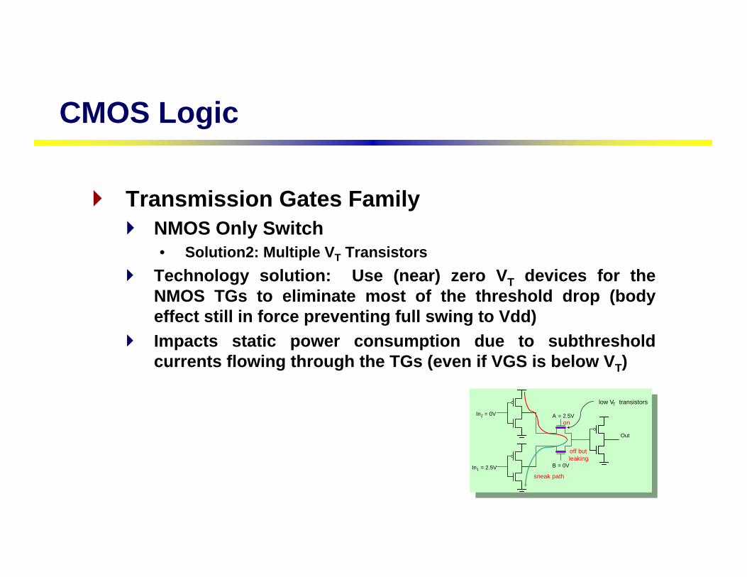
Transmission Gates FamilyNMOS Only Switch• Solution2: Multiple VT Transistors
Technology solution: Use (near) zero VT devices for the NMOS TGs to eliminate most of the threshold drop (body effect still in force preventing full swing to Vdd)Impacts static power consumption due to subthresholdcurrents flowing through the TGs (even if VGS is below VT)
CMOS Logic
Out
In2 = 0V
In1 = 2.5V
A = 2.5V
B = 0V
low VT transistors
sneak path
on
off but leaking
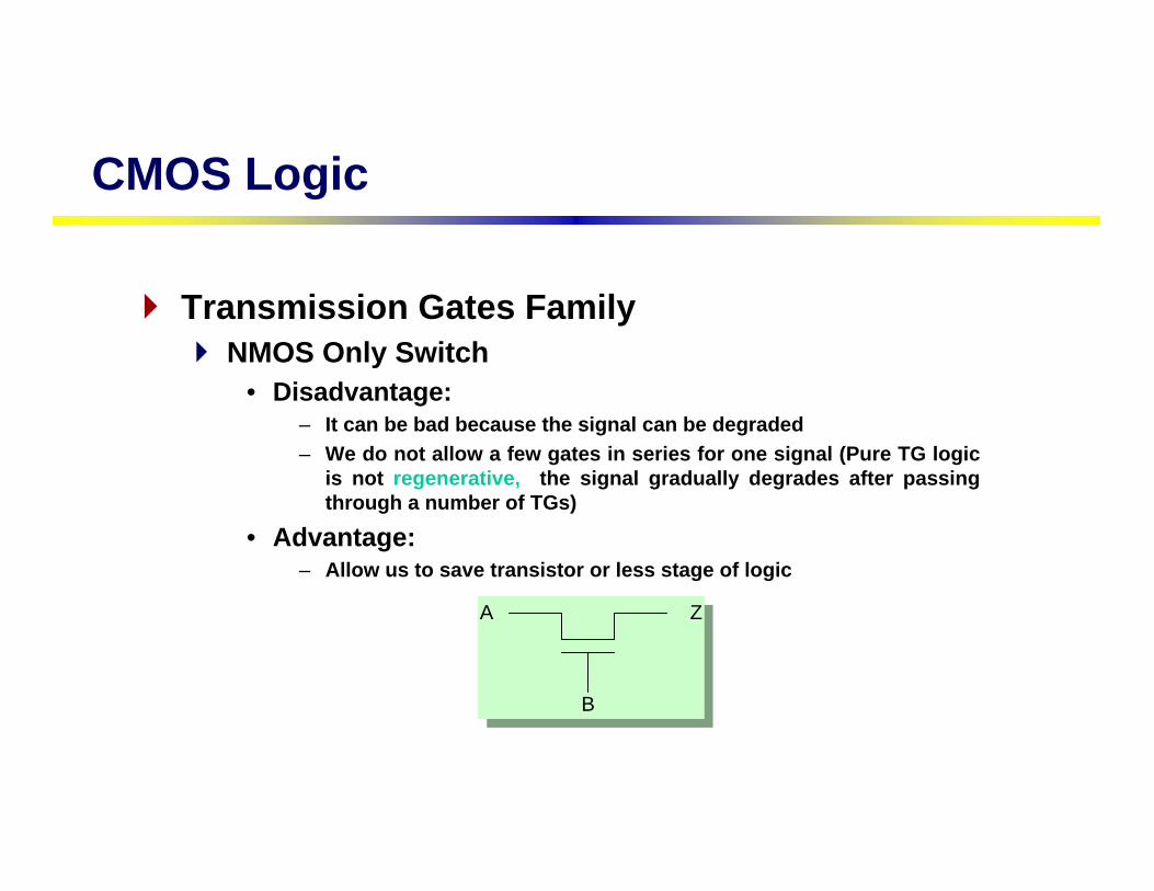
Transmission Gates FamilyNMOS Only Switch
• Disadvantage:– It can be bad because the signal can be degraded– We do not allow a few gates in series for one signal (Pure TG logic
is not regenerative, the signal gradually degrades after passing through a number of TGs)
• Advantage:– Allow us to save transistor or less stage of logic
CMOS Logic
ZA
B
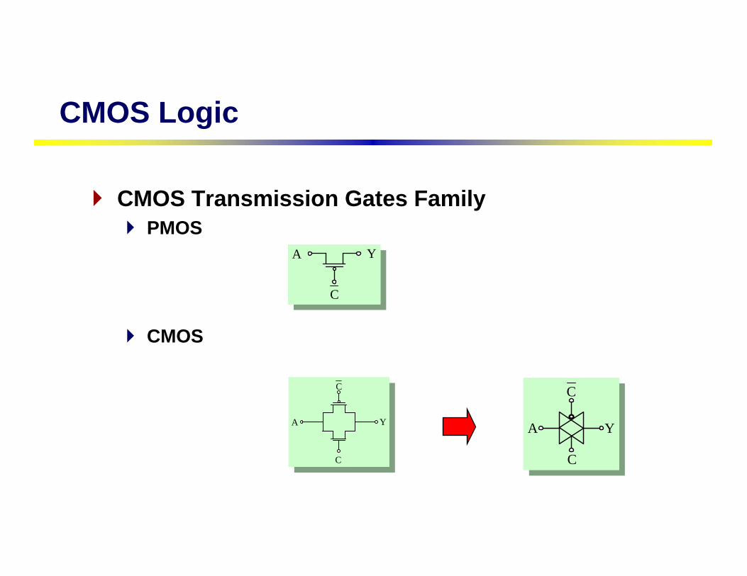
CMOS Transmission Gates FamilyPMOS
CMOS
A Y
C
CMOS Logic
C
C
A Y A Y
C
C
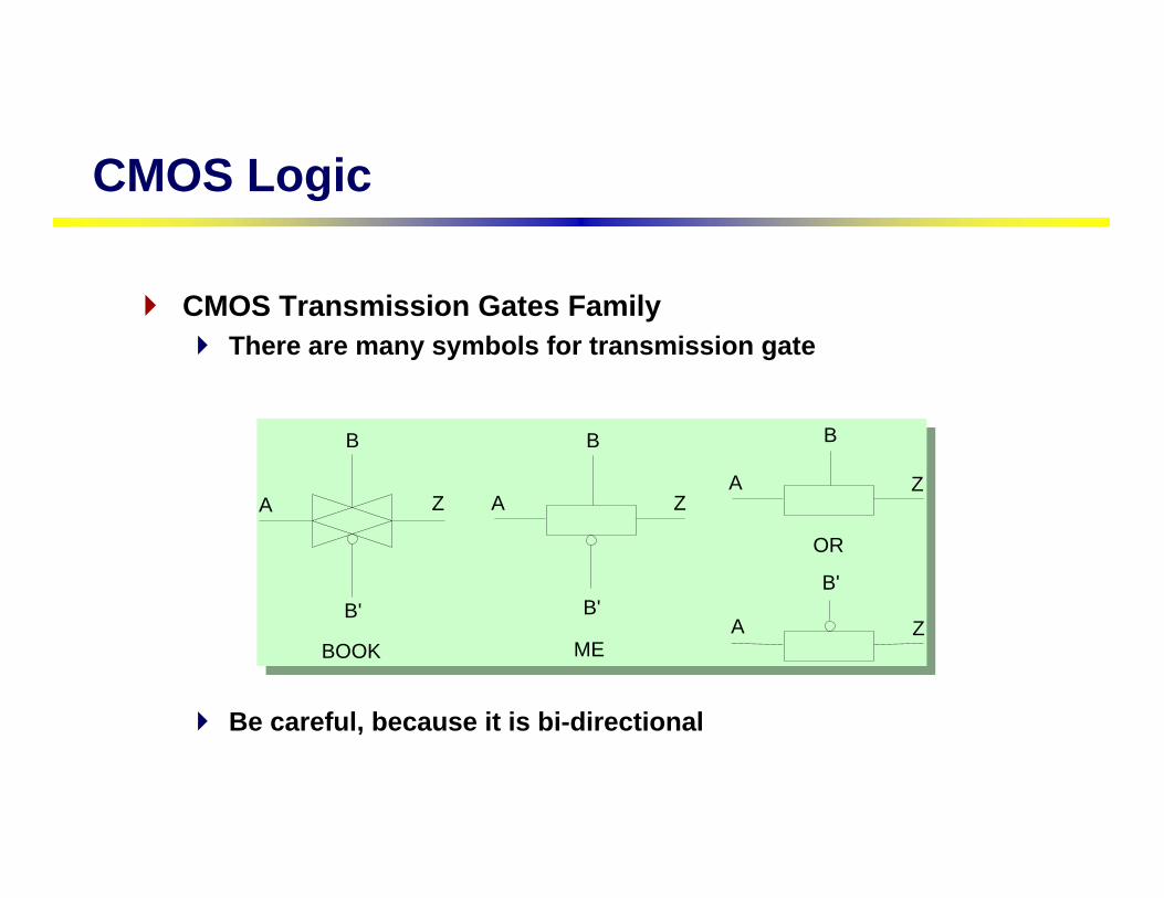
CMOS Transmission Gates FamilyThere are many symbols for transmission gate
Be careful, because it is bi-directional
B'
B
A Z
B'
B
A Z
B
A Z
OR
B'
A ZBOOK ME
CMOS Logic
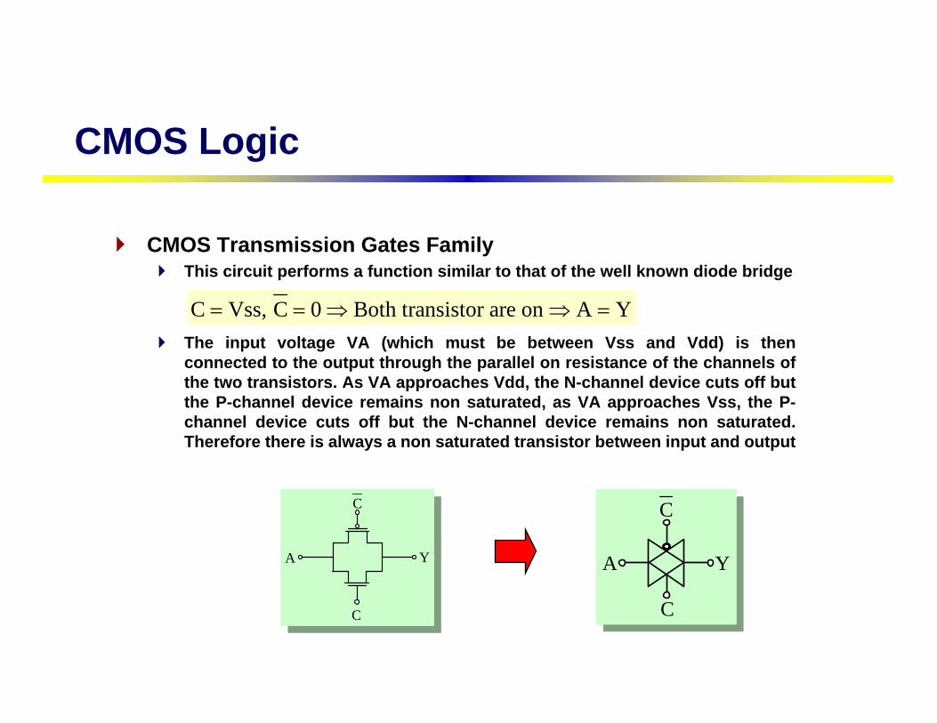
CMOS Transmission Gates FamilyThis circuit performs a function similar to that of the well known diode bridge
The input voltage VA (which must be between Vss and Vdd) is then connected to the output through the parallel on resistance of the channels of the two transistors. As VA approaches Vdd, the N-channel device cuts off but the P-channel device remains non saturated, as VA approaches Vss, the P-channel device cuts off but the N-channel device remains non saturated. Therefore there is always a non saturated transistor between input and output
CMOS Logic
C
C
A Y A Y
C
C
C Vss, C 0 Both transistor are on A Y= = ⇒ ⇒ =

C
C
A YCL
PI
NI
S
D
t
VA
Vdd
Vy
CMOS Transmission Gates FamilyFor more understanding note to this circuitWe assume:
CMOS Logic
TP TNVy(0 ) 0, C Vdd, C 0, V Vdd V− = = = < −

C
C
A YCL
PI
NI
CMOS Transmission Gates Family
CMOS Logic
TP
TP TN
TN
CL N PVy V
PVy V Vy Vdd V
PVy Vdd V Vy Vdd
N sat0 t t I I I
P sat
N satt t t r CL
P triode
N offt t t r CL
P triode
=
= = −
= − =
=⎧≤ ≤ ⇒ ⇒ = +⎨ =⎩
=⎧≤ ≤ ⇒ ⇒ τ ≈⎨ =⎩
=⎧≤ ≤ ⇒ ⇒ τ ≈⎨ =⎩

C
C
A YCL
PI
NI
CMOS Transmission Gates FamilyIt is normally assumed as a resistor
CMOS Logic
A
TG
TG TG
TG N P
V (t) Vddu(t)
tVy(t) Vdd 1 exp u(t)
R CLR r r
=
⎡ ⎤⎛ ⎞−= −⎢ ⎥⎜ ⎟
τ⎢ ⎥⎝ ⎠⎣ ⎦τ =
=
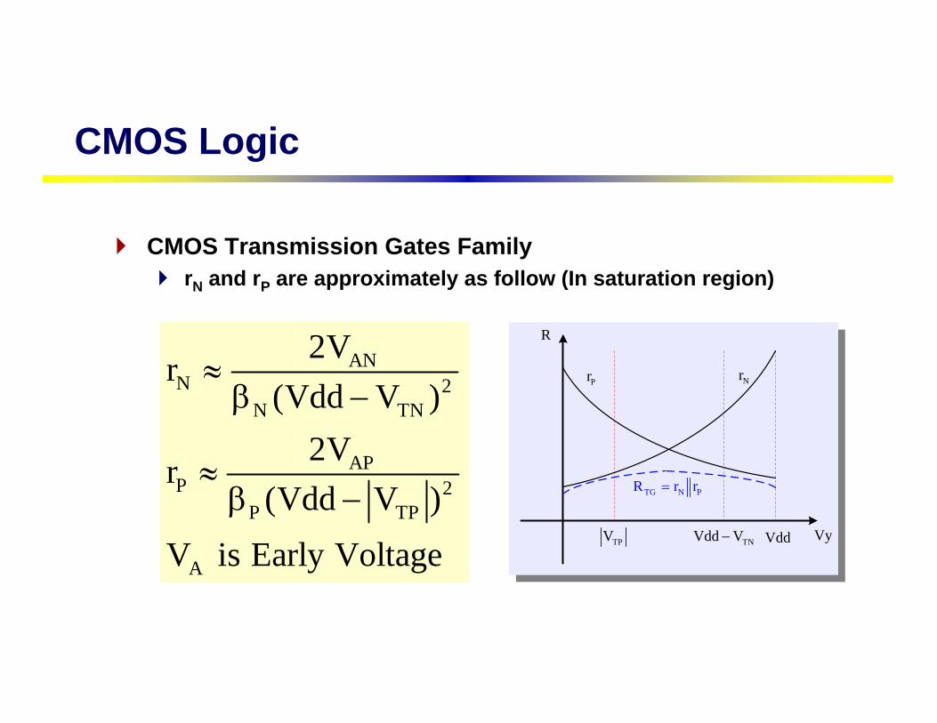
CMOS Transmission Gates FamilyrN and rP are approximately as follow (In saturation region)
ANN 2
N TN
APP 2
P TP
A
2Vr
(Vdd V )2V
r(Vdd V )
V is Early Voltage
≈β −
≈β −
CMOS Logic
R
VyTPV TNVdd V− Vdd
Pr Nr
TG N PR r r=

CMOS Transmission Gates FamilyWhat to note about TG
• The inputs must be able to give high current because they are connected directly to Drain and Source of transistors
• Since each input is connected to an RC circuit, The delay can be considered directly
• Limited Fan-in• Excessive Fan-out• Noise vulnerability (not restoring)• Supply voltage offset/bias vulnerability• Poor high voltage levels if NMOS-only• Body effect
CMOS Logic

CMOS Transmission Gates Family Rules of Thumb• Pass-Logic may consume half the power of static logic. But be
careful of VT drop resulting in static leakage • Pass-Gate Logic is not appropriate when long interconnects
separate logic stages or when circuits have high Fan-out load (use buffering)
CMOS Logic
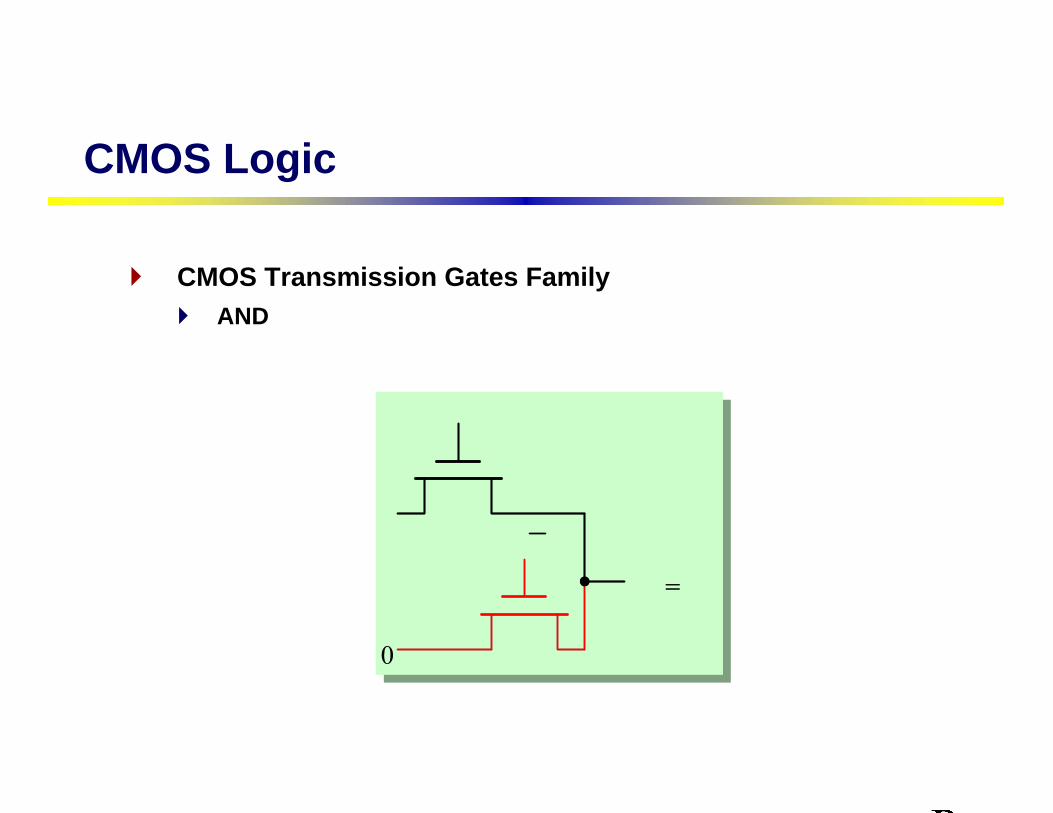
CMOS Transmission Gates FamilyAND
CMOS Logic
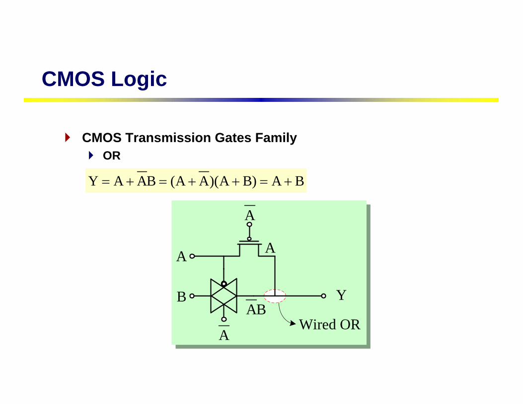
CMOS Transmission Gates FamilyOR
Y A AB (A A)(A B) A B= + = + + = +
CMOS Logic
A
Y
A
BAB
A
A
Wired OR

CMOS Transmission Gates FamilyMUX
A S 1Y
B S 0=⎧
= ⎨ =⎩
CMOS Logic
A
Y
S
B
S
S
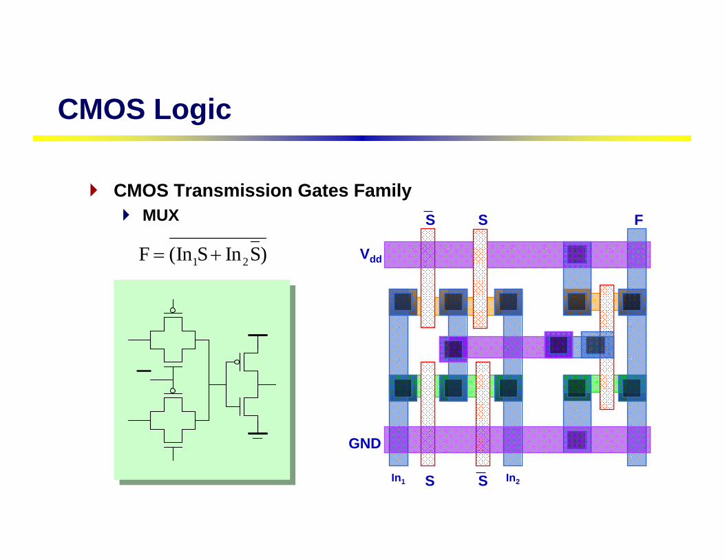
CMOS Transmission Gates FamilyMUX
CMOS Logic
GND
Vdd
In1 In2S S
S S F
1 2F (In S In S)= +
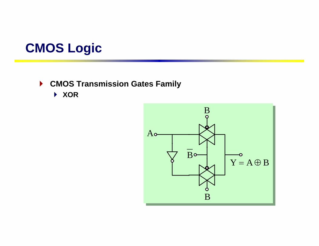
CMOS Transmission Gates FamilyXOR
CMOS Logic
A
Y A B= ⊕
B
B
B

CMOS Transmission Gates FamilyXNOR
CMOS Logic
A
Y AB AB= +B
B
B
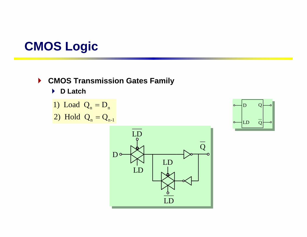
CMOS Transmission Gates FamilyD Latch
CMOS Logic
D
LD
Q
Q
n n
n n-1
1) Load Q D2) Hold Q Q
==
DQ
LD
LD
LDLD

CMOS Transmission Gates FamilyD Latch
CMOS Logic
1) Load LD 1=
2) Hold LD 0=
D Q D=
D Q=
Q
Q

CMOS Transmission Gates FamilyD Latch (Simpler Realization)
• If in Load Mode a level voltage opposite to the output of weak inverter is applied to the input by TG, Q = D and weak inverter is not damaged!
CMOS Logic
DQ
LD
LD
QWeak Inverter
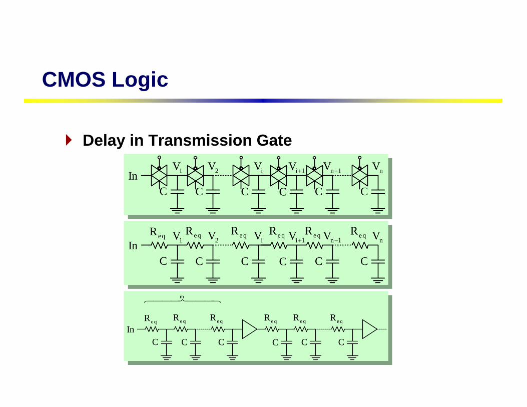
C C C C C C
e qR e qR e qR e qR e qR e qRIn
m
644474448
C C C C C C
e qR e qR e qR e qR e qR e qRIn 1V 2V iV i 1V + n 1V − nV
C C C C C CIn 1V 2V iV i 1V + n 1V − nV
CMOS Logic
Delay in Transmission Gate

Delay OptimizationDelay of RC chain
Delay of Buffered chain
n
P e q eqk 1
n(n 1)t 0.69 C R k 0.69C R2=
+= =∑
CMOS Logic
P e q buf
e q buf
Pbufopt
e q
n m(m 1) nt 0.69 C R 1 tm 2 m
n(m 1) n0.69 C R 1 t2 m
tm 1.7
C R
+⎡ ⎤ ⎛ ⎞= + −⎜ ⎟⎢ ⎥⎣ ⎦ ⎝ ⎠+⎡ ⎤ ⎛ ⎞= + −⎜ ⎟⎢ ⎥⎣ ⎦ ⎝ ⎠
=
CMOS Logic
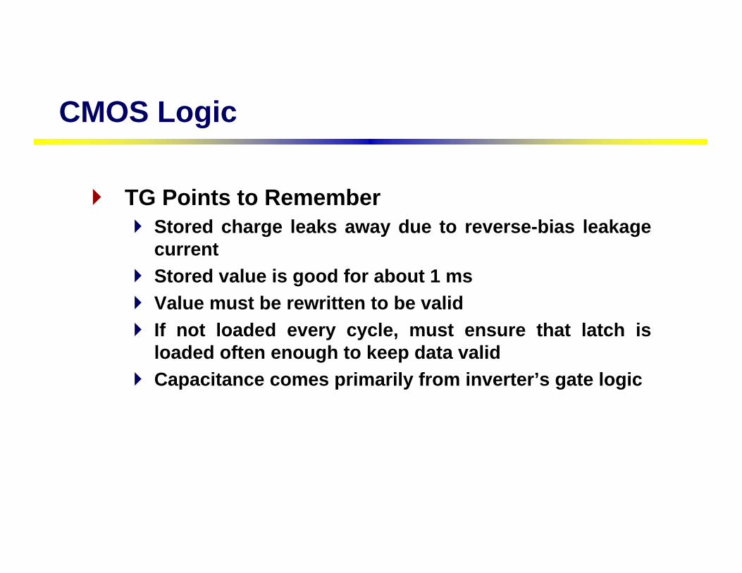
TG Points to RememberStored charge leaks away due to reverse-bias leakage currentStored value is good for about 1 msValue must be rewritten to be validIf not loaded every cycle, must ensure that latch is loaded often enough to keep data validCapacitance comes primarily from inverter’s gate logic
CMOS Logic
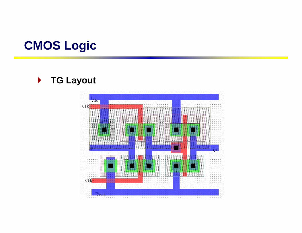
TG Layout
CMOS Logic
TG PropertiesStrong pull-upStrong pull-downMay be difficult to design into a circuit (layout) because of close proximity of N and P devices (design rule separation)Always requires 2N transisitors for any N x TG designMany logic functions (multiplexers in particular) are easily implemented using TG based designs

Complementary Pass-transistor Logic (CPL) or Differential (+) TG Logic
Dual-rail form of pass transistor logicAvoids need for ratioed feedback
B
S
S
S
S
A
B
AY
YL
L
CMOS Logic
A
B
AB
PT Network F
A
B
AB
Inverse PT Network F
F
F
CMOS Logic
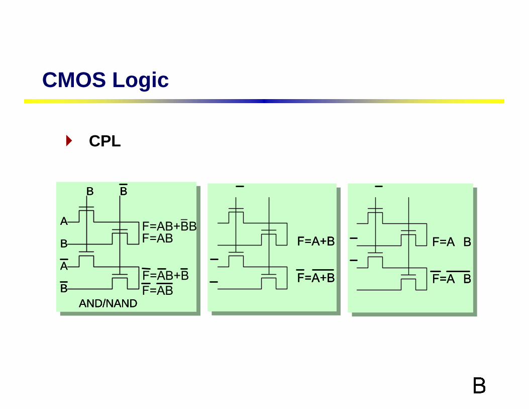
CPL
A
A
B
B
B B
AND/NAND
A
A
B
B
B B
AND/NAND
A
A
B
BB
B BB
AND/NAND

CMOS Logic
4 Input NAND in CPL

CMOS Logic
CPL AdvantagesDifferential so complementary data inputs and outputs are always available (so don’t need extra inverters)Still static, since the output defining nodes are always tied to Vdd or GND through a low resistance pathDesign is modular, all gates use the same topology, only the inputs are permutedSimple XOR makes it attractive for structures like addersFast (assuming number of transistors in series is small)
CMOS Logic
CPL DisadvantagesAdditional routing overhead for complementary signalsStill have static power dissipation problemsVOH is very weak! Then we need an inverter at the output
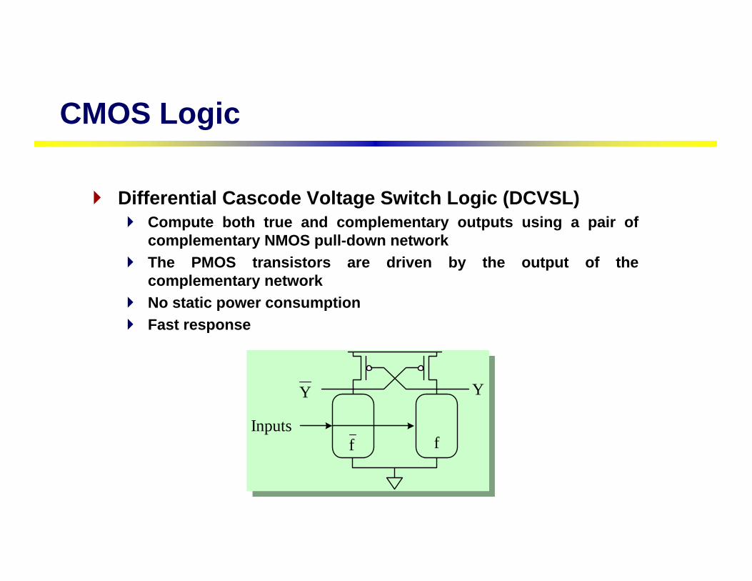
Differential Cascode Voltage Switch Logic (DCVSL)Compute both true and complementary outputs using a pair of complementary NMOS pull-down networkThe PMOS transistors are driven by the output of the complementary networkNo static power consumptionFast response
CMOS Logic
Inputs
Y Y
f f

Differential Cascode Voltage Switch Logic (DCVSL)Example: NAND/AND
CMOS Logic
Y AB=
BA
A
B
Y A B= +
Series⎫⎬⎭

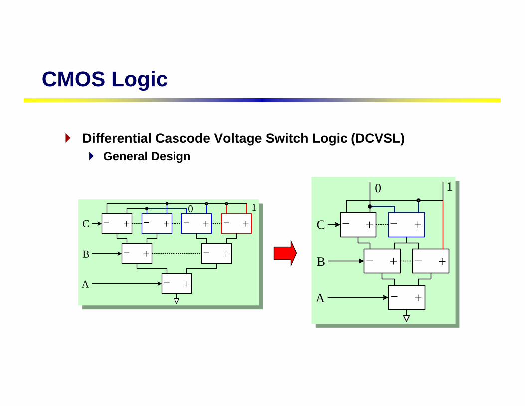
Differential Cascode Voltage Switch Logic (DCVSL)General Design
11111011110100011110001001001000FCBA
CMOS Logic
+ + + +
++
+
_ _ _ _
__
_A
B
C0 1

Differential Cascode Voltage Switch Logic (DCVSL)General Design
+_x
a b
u
x x
a b
uu ax bx= +
≡
CMOS Logic
+_x
u
≡
u
+_x
a b
1u
+_
a b
2u
+_x
a b
1u
≡
2u
Differential Cascode Voltage Switch Logic (DCVSL)General Design
+ + + +
++
+
_ _ _ _
__
_A
B
C0 1
CMOS Logic
+ +
++
+
_ _
__
_A
B
C
0 1
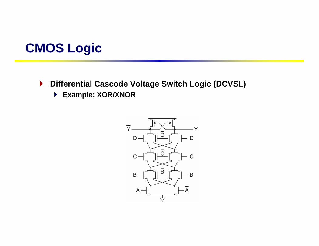
Differential Cascode Voltage Switch Logic (DCVSL)Example: XOR/XNOR
CMOS Logic
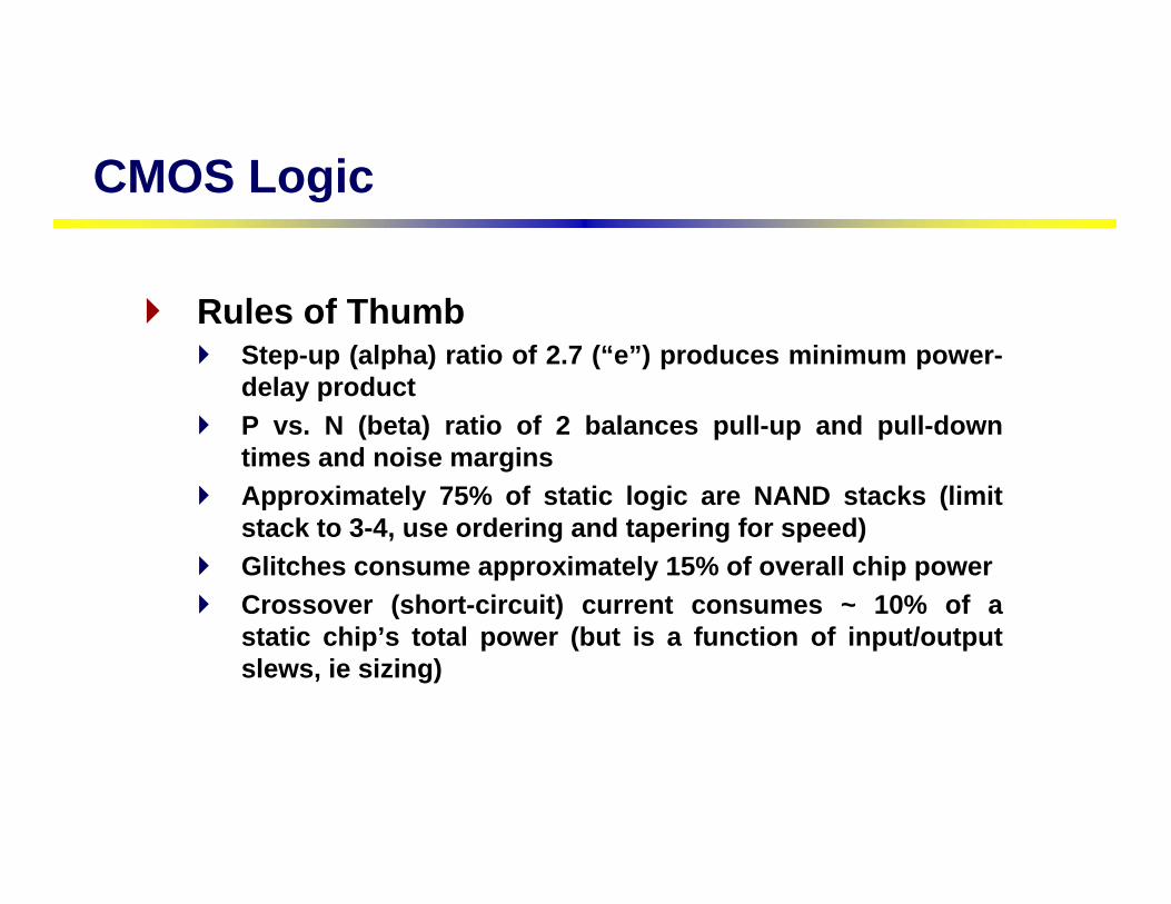
Rules of ThumbStep-up (alpha) ratio of 2.7 (“e”) produces minimum power-delay productP vs. N (beta) ratio of 2 balances pull-up and pull-down times and noise marginsApproximately 75% of static logic are NAND stacks (limit stack to 3-4, use ordering and tapering for speed)Glitches consume approximately 15% of overall chip powerCrossover (short-circuit) current consumes ~ 10% of a static chip’s total power (but is a function of input/output slews, ie sizing)
CMOS Logic
Summary
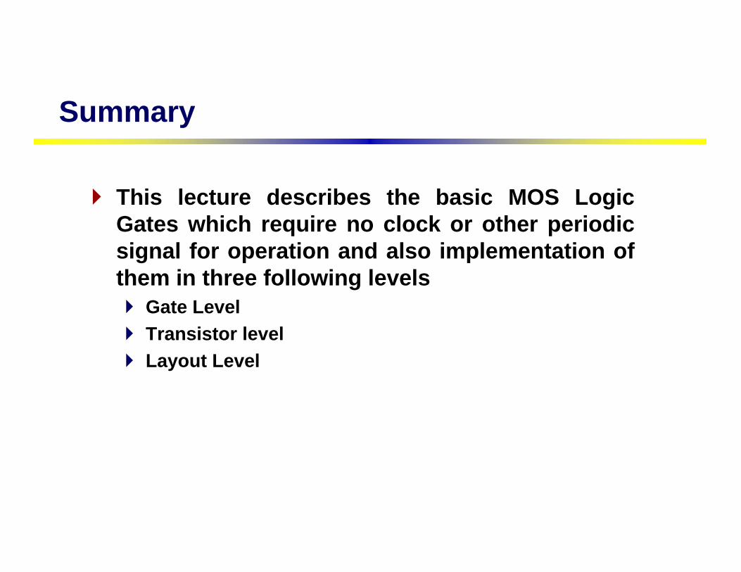
This lecture describes the basic MOS Logic Gates which require no clock or other periodic signal for operation and also implementation of them in three following levels
Gate LevelTransistor levelLayout Level
Contents
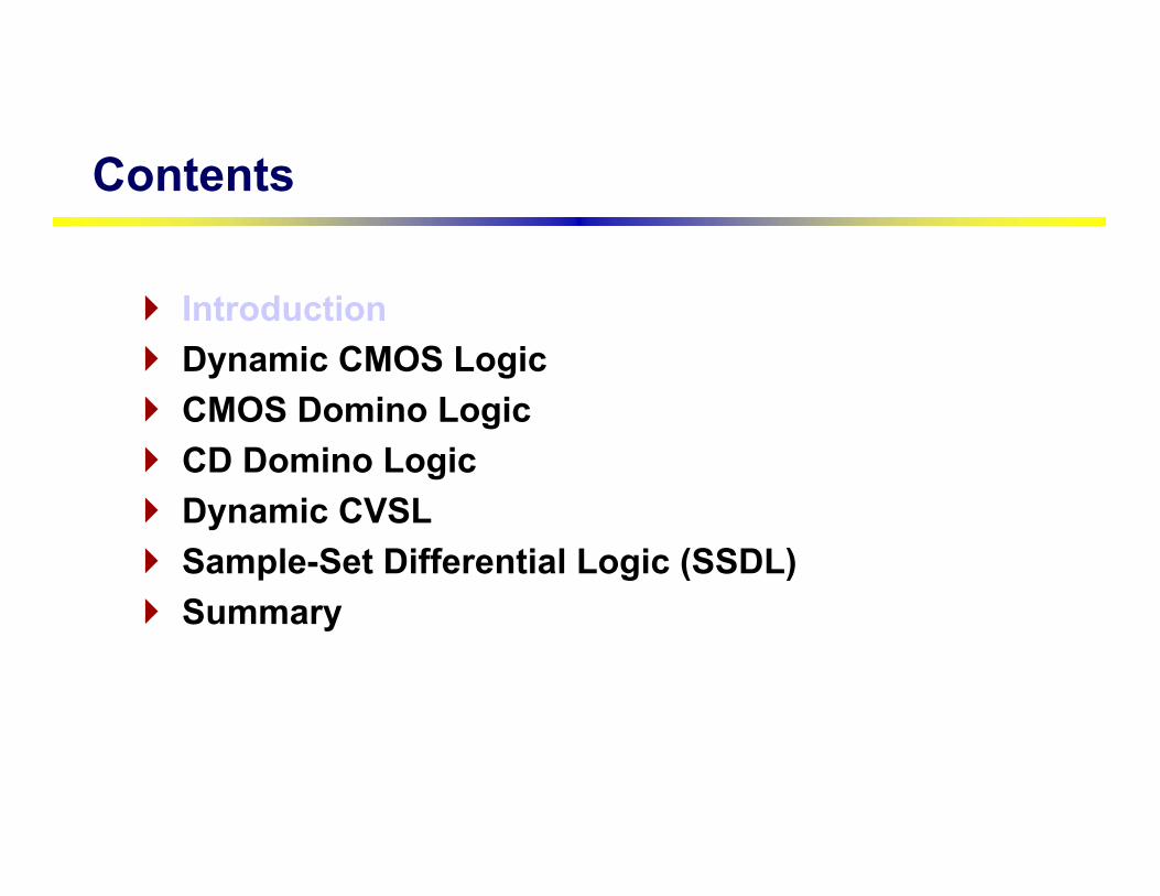
IntroductionDynamic CMOS LogicCMOS Domino LogicCD Domino LogicDynamic CVSLSample-Set Differential Logic (SSDL)Summary
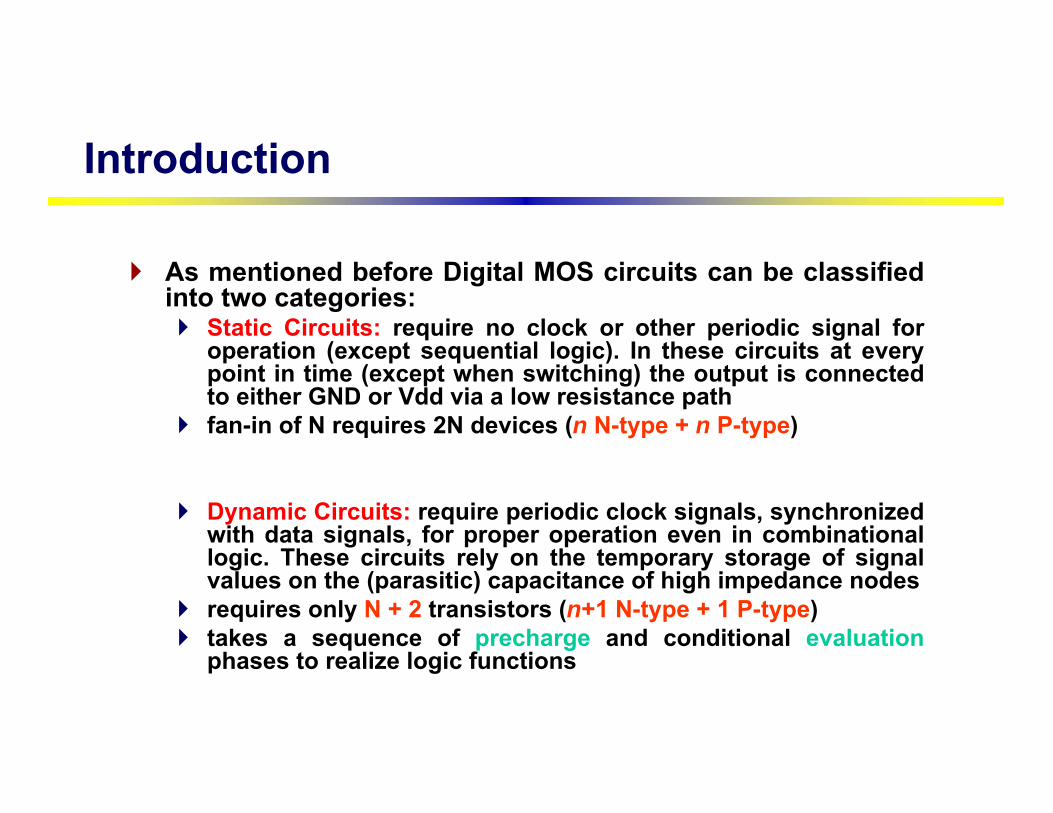
As mentioned before Digital MOS circuits can be classified into two categories:
Static Circuits: require no clock or other periodic signal for operation (except sequential logic). In these circuits at every point in time (except when switching) the output is connected to either GND or Vdd via a low resistance pathfan-in of N requires 2N devices (n N-type + n P-type)
Dynamic Circuits: require periodic clock signals, synchronized with data signals, for proper operation even in combinational logic. These circuits rely on the temporary storage of signal values on the (parasitic) capacitance of high impedance nodesrequires only N + 2 transistors (n+1 N-type + 1 P-type) takes a sequence of precharge and conditional evaluationphases to realize logic functions
Introduction

Why Dynamic Logic?In the area of high speed, higher Fan-in, extremely low power dissipation, other digital logic circuit have been considered. In this lecture, two of these alternatives to CMOS are described. The circuits are basically NMOS or CMOS Gates with slight improvements. These are:
Dynamic CMOS LogicCMOS Domino Logic
Each of them have specific operating advantages over NMOS or CMOS, but exhibit disadvantages in other areas
Introduction

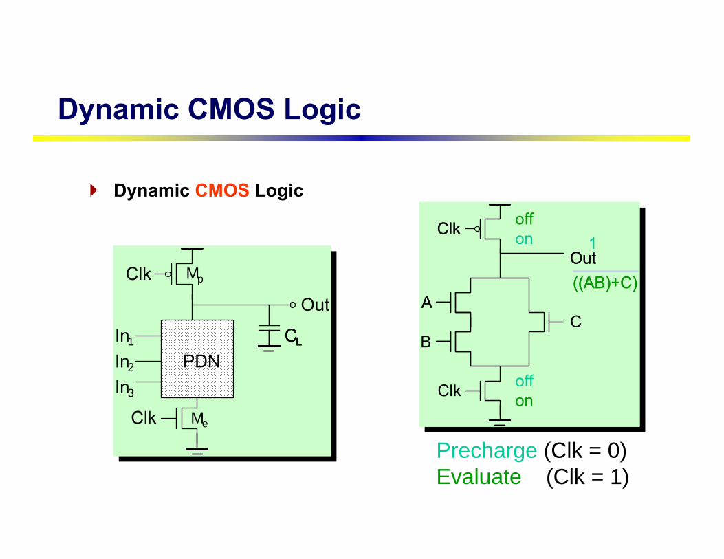
Dynamic Gates use a clocked PMOS pullupTwo modes: precharge and evaluate
φ Precharge Evaluate
Y
Precharge
Dynamic CMOS Logic
The FootWhat if pulldown network is ON during precharge?Use series evaluation transistor to prevent fight
AY
φ
foot
precharge transistor
Dynamic CMOS Logic
Dynamic CMOS Logic
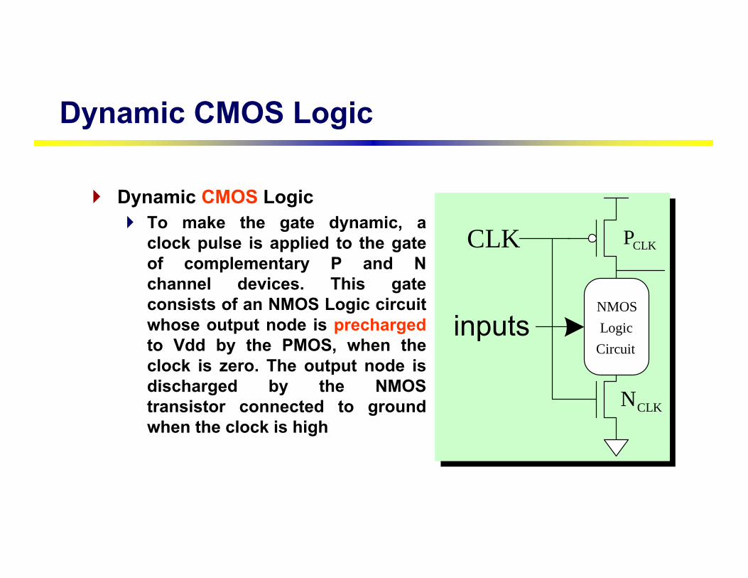
Dynamic CMOS LogicTo make the gate dynamic, a clock pulse is applied to the gate of complementary P and N channel devices. This gate consists of an NMOS Logic circuit whose output node is prechargedto Vdd by the PMOS, when the clock is zero. The output node is discharged by the NMOS transistor connected to ground when the clock is high
NMOSLogic
Circuit
CLKP
CLKN
CLK
Precharge (Clk = 0)Evaluate (Clk = 1)
Dynamic CMOS Logic
1
2
3
Me
Mp
LL
Dynamic CMOS Logic
Once the output of a dynamic gate is discharged, it cannot be charged again until the next precharge operationInputs to the gate can make at most one transition during evaluationOutput can be in the high impedance state during and after evaluation (PDN off), state is stored on CL
Dynamic CMOS Logic
Dynamic CMOS Logic
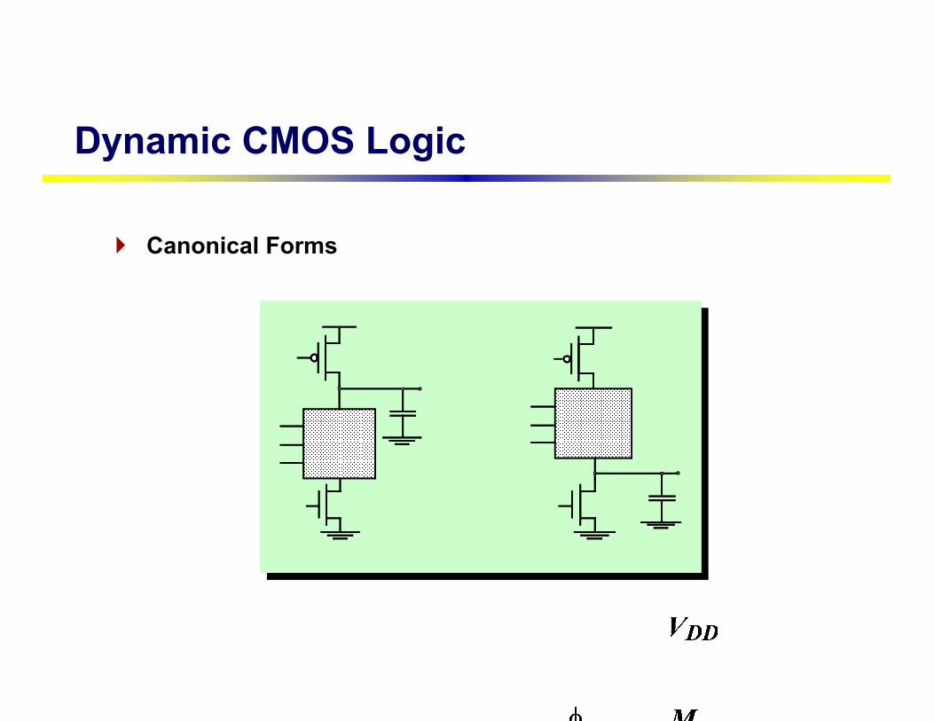
Canonical Forms

Dynamic CMOS Logic
Properties of Dynamic GatesLogic function is implemented by the PDN only
• should be smaller in area than static complementary CMOSFull swing outputs (VOL = GND and VOH = VDD)Nonratioed - sizing of the devices is not important for proper functioning (only for performance)Faster switching speeds
• reduced load capacitance due to lower number of transistors per gate (Cint) so a reduced logical effort
• reduced load capacitance due to smaller fan-out (Cext)• no Isc, so all the current provided by PDN goes into discharging
CL
• Ignoring the influence of precharge time on the switching speed of the gate, tpLH = 0 but the presence of the evaluation transistor slows down the tpHL

Dynamic CMOS Logic
Properties of Dynamic GatesPower dissipation should be better
• consumes only dynamic power – no short circuit power consumption since the pull-up path is not on when evaluating
• lower CL- both Cint (since there are fewer transistors connected to the drain output) and Cext (since there the output load is one per connected gate, not two)
But power dissipation can be significantly higher due to• higher transition probabilities• extra load on CLK
PDN starts to work as soon as the input signals exceed VTn, so set VM, VIH and VIL all equal to VTn
• low noise margin (NML)Needs a precharge/evaluate clock
Dynamic CMOS Logic
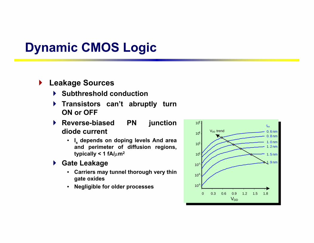
Leakage SourcesSubthreshold conductionTransistors can’t abruptly turn ON or OFFReverse-biased PN junction diode current
• Is depends on doping levels And area and perimeter of diffusion regions, typically < 1 fA/µm2
Gate Leakage• Carriers may tunnel thorough very thin
gate oxides• Negligible for older processes
VDD
0 0.3 0.6 0.9 1.2 1.5 1.8
10-9
10-6
10-3
100
103
106
109
tox
0. 6 nm0. 8 nm
1. 0 nm1. 2 nm
1. 5 nm
1. 9 nm
VDD trend
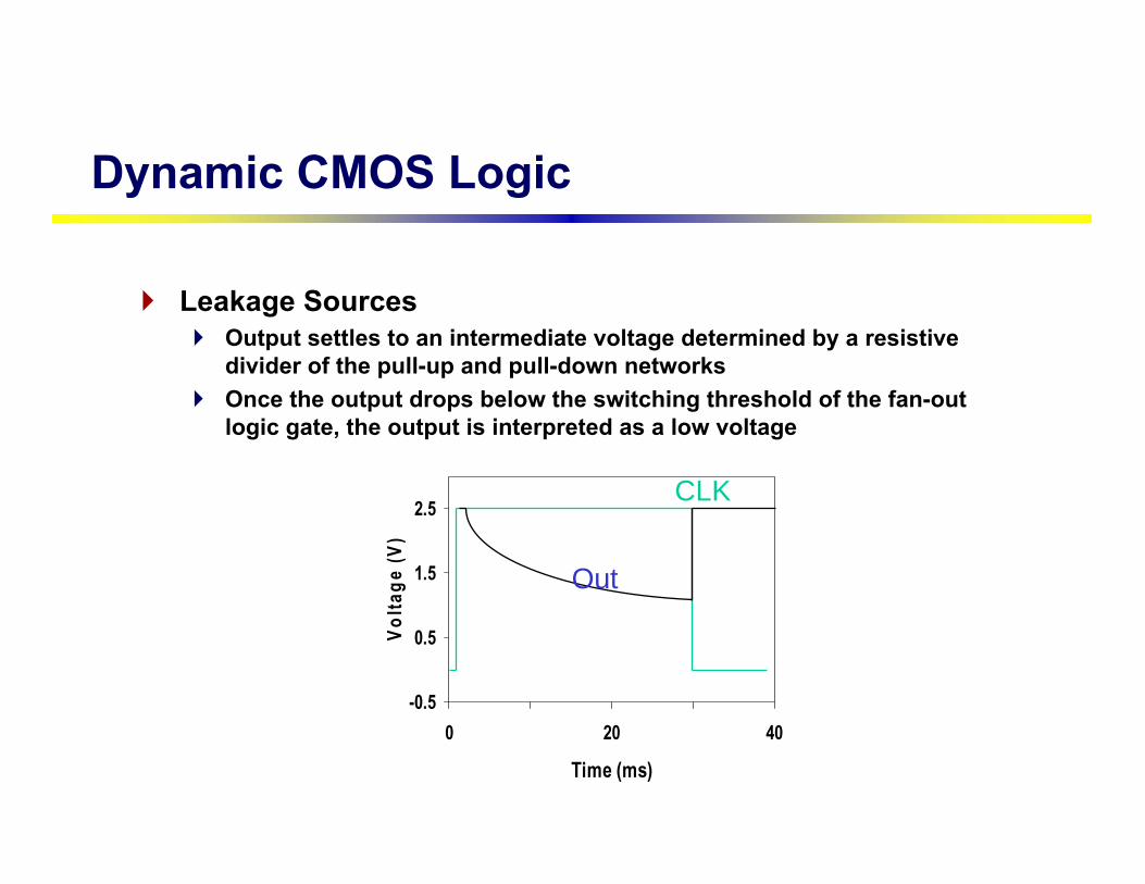
Leakage SourcesOutput settles to an intermediate voltage determined by a resistive divider of the pull-up and pull-down networksOnce the output drops below the switching threshold of the fan-out logic gate, the output is interpreted as a low voltage
Dynamic CMOS Logic
-0.5
0.5
1.5
2.5
0 20 40
Time (ms)
Volta
ge (V
)
CLK
Out
Leakage sources
CLK
VOut
Precharge
Evaluate
Dynamic CMOS Logic
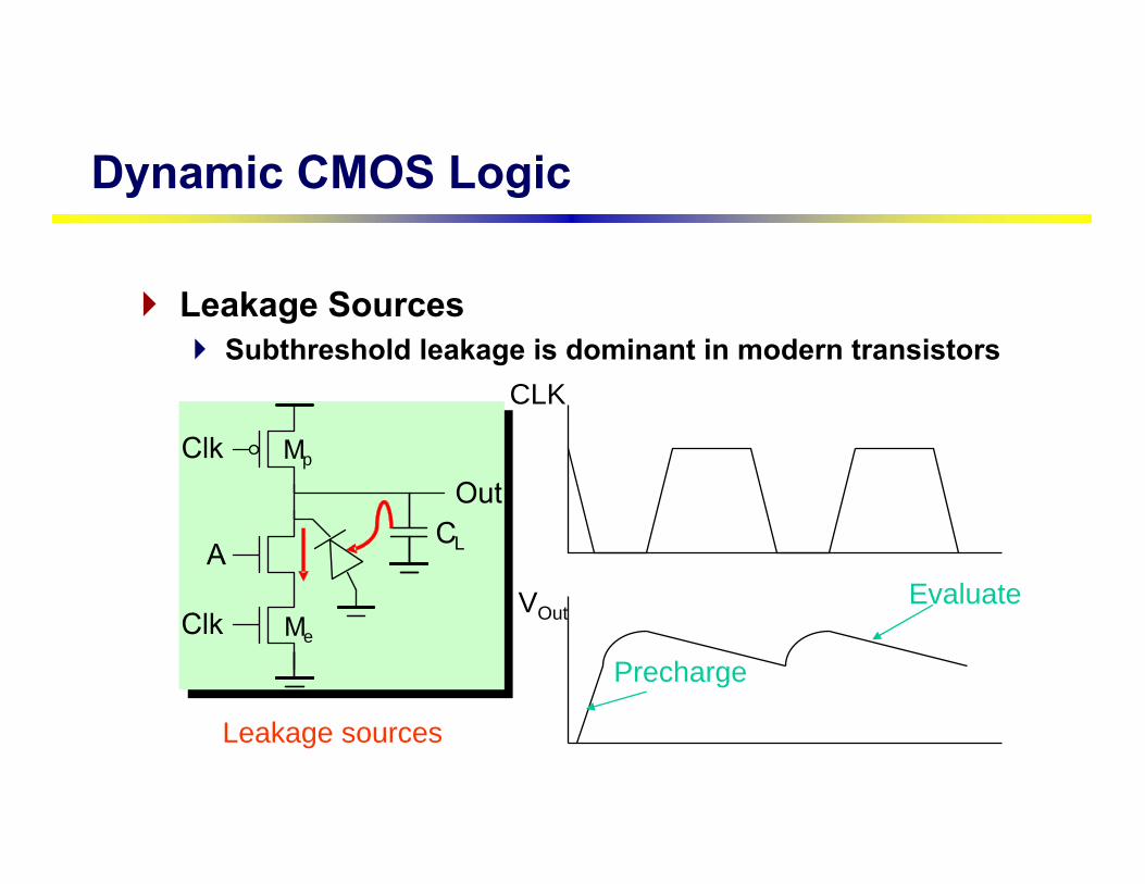
Leakage SourcesSubthreshold leakage is dominant in modern transistors
L
p
e
Dynamic CMOS Logic
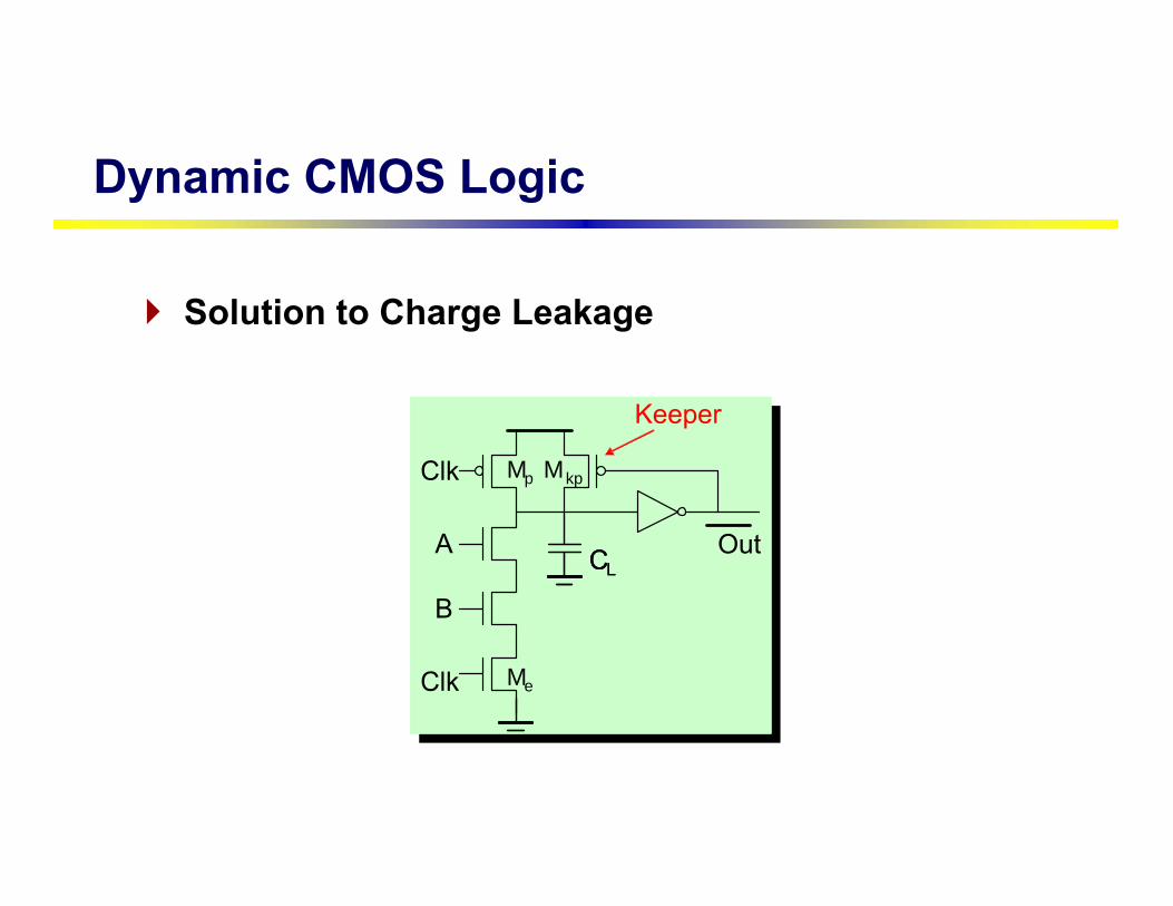
Solution to Charge Leakage
LL
Me
Mp Mkp

Charge SharingCharge stored originally on CY is redistributed (shared) over CXleading to static power consumption by downstream gates and possible circuit malfunctionWhen ∆Vout = - Vdd (CX / (CX + CY )) the drop in Vout is large enough to be below the switching threshold of the gate it drivescausing a malfunction
B = 0
AY
φ
x
Cx
CY
A
φ
x
Y
Charge sharing noise
= =+Y
x Y ddx Y
CV V VC C
Dynamic CMOS Logic

Solution to Charge Redistribution Add secondary precharge transistors (at the cost of increased area and power)
• Typically need to precharge every other node• Secondary precharge transistors should be small because their
diffusion capacitance slows the evaluation (increase delay)• Big load capacitance CY helps as well
B
AY
x
secondaryprechargetransistor
Dynamic CMOS Logic
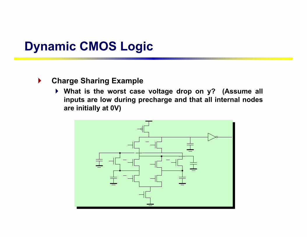
Charge Sharing ExampleWhat is the worst case voltage drop on y? (Assume all inputs are low during precharge and that all internal nodes are initially at 0V)
Dynamic CMOS Logic
Dynamic CMOS Logic
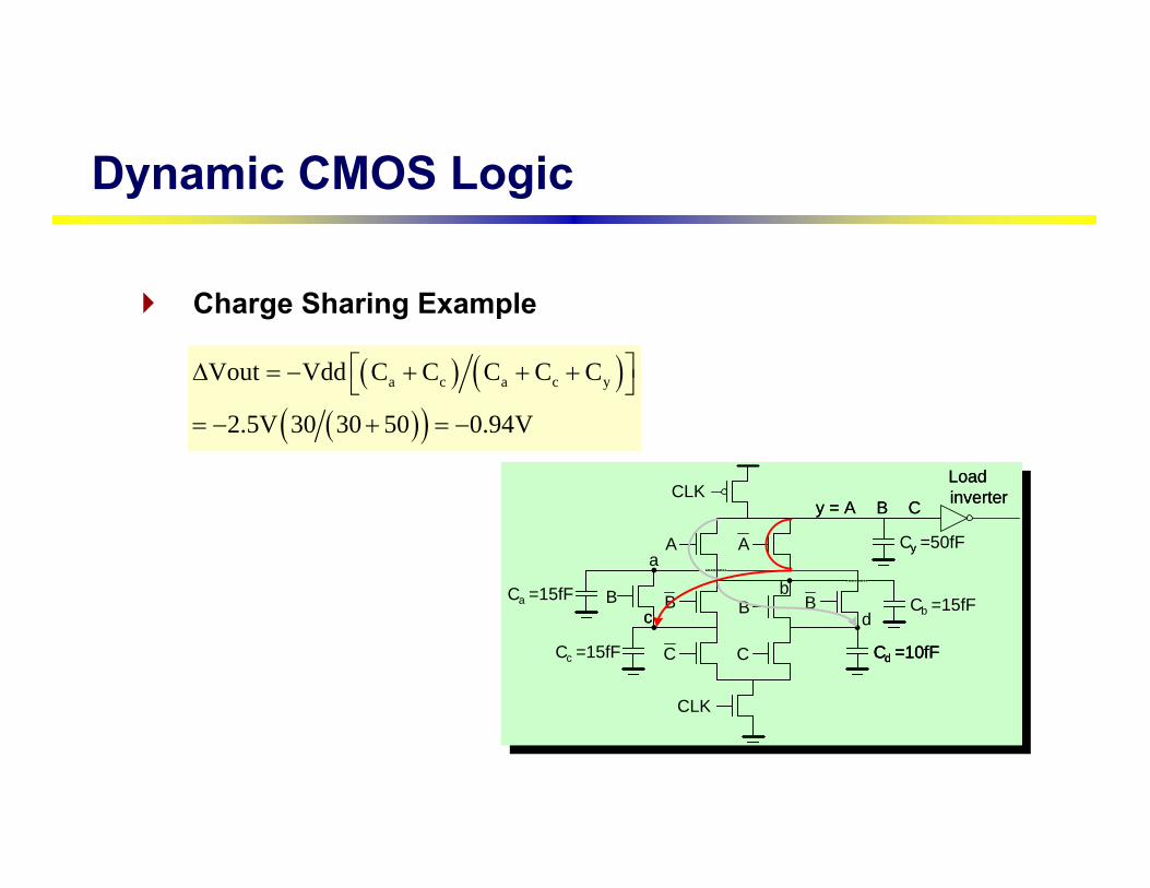
Charge Sharing Example
y
CLK
CLK
A A
B B B
CC
y = A B C
Ca =15fF
Cc =15fF
Cb =15fF
Cd =10fF
Loadinverter
ab
dc
Cy =50fF
y = A B C
Cd =10fFCd =10fF
Loadinverter
cB
( ) ( )( )( )
a c a c yVout Vdd C C C C C
2.5V 30 30 50 0.94V
⎡ ⎤∆ = − + + +⎣ ⎦
= − + = −
Dynamic CMOS Logic
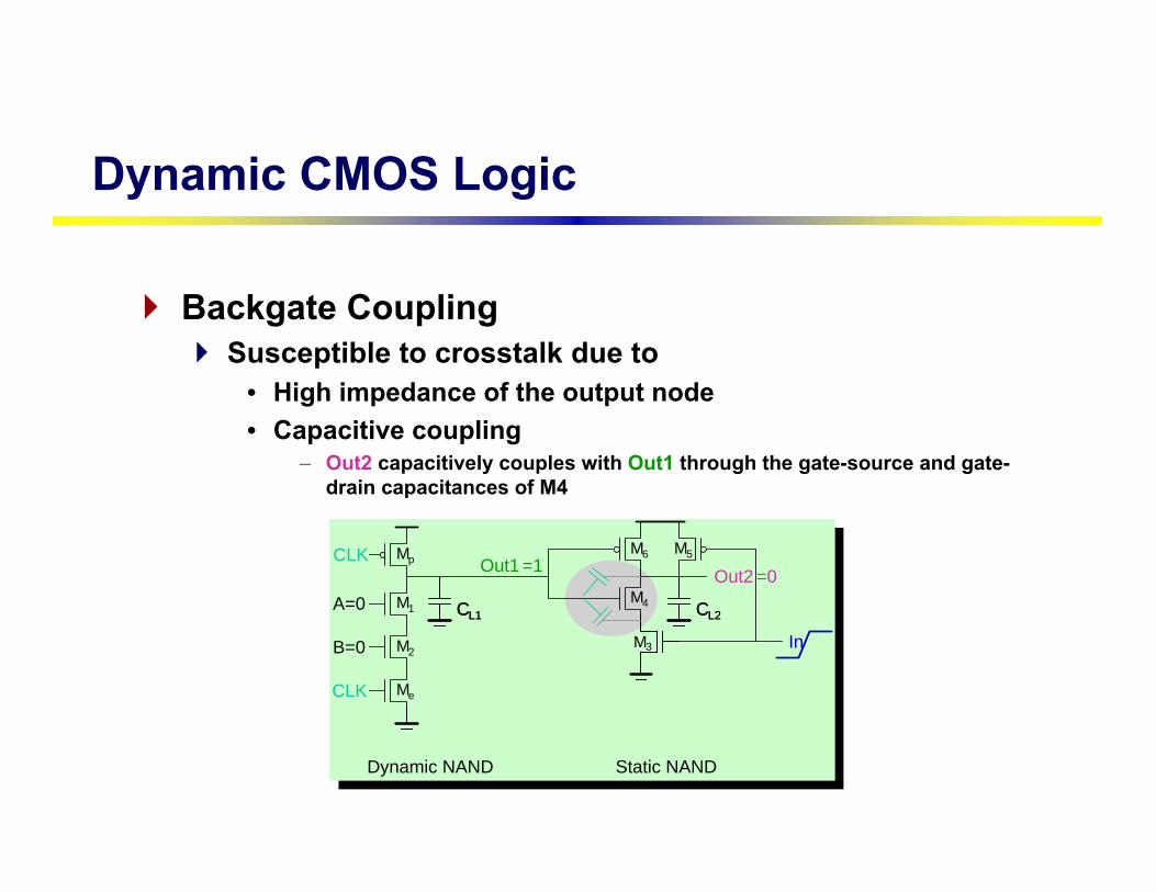
Backgate CouplingSusceptible to crosstalk due to
• High impedance of the output node • Capacitive coupling
– Out2 capacitively couples with Out1 through the gate-source and gate-drain capacitances of M4
CL1CL1
CLK
CLK
B=0
A=0
Out1Mp
Me
Out2
CL2CL2
In
Dynamic NAND Static NAND
=1 =0M1
M2M3
M4
M5M6

Capacitive coupling means Out1 drops significantly so Out2 doesn’t go all the way to ground
Dynamic CMOS Logic
Backgate Coupling
-1
0
1
2
3
0 2 4 6
Vol
tage
Time, ns
Clk
In
Out1
Out2
Due to backgate
Due to clk feedthrough
Dynamic CMOS Logic
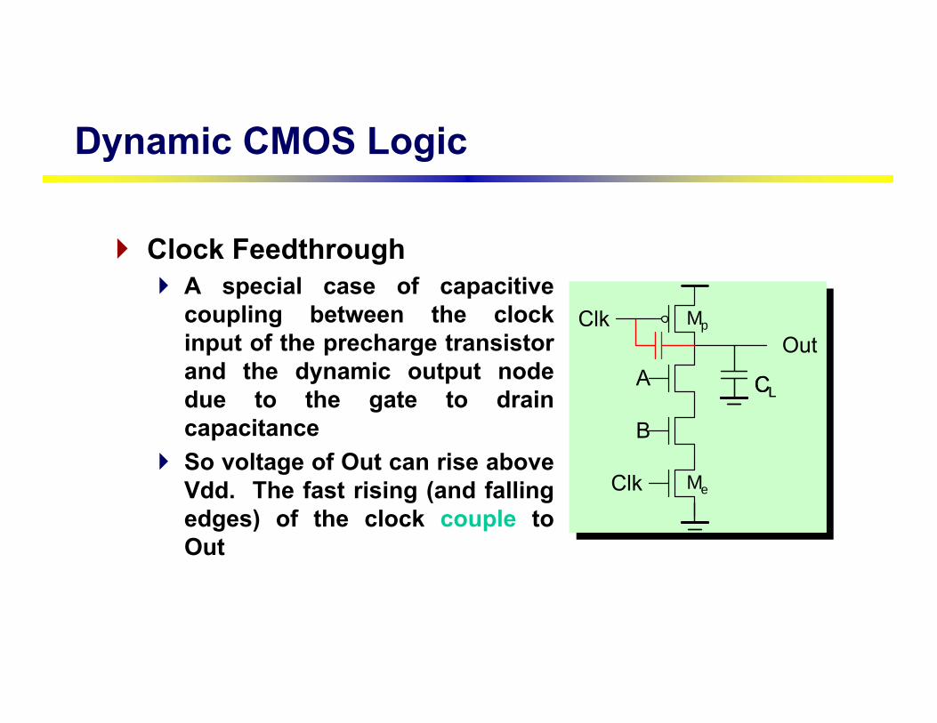
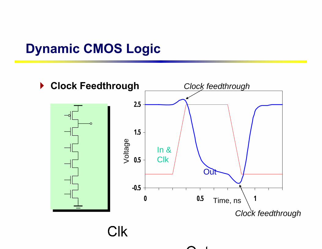
Clock FeedthroughA special case of capacitive coupling between the clock input of the precharge transistor and the dynamic output node due to the gate to drain capacitanceSo voltage of Out can rise above Vdd. The fast rising (and falling edges) of the clock couple to Out
LL
Mp
Me
-0.5
0.5
1.5
2.5
0 0.5 1
In &Clk
Out
Time, ns
Vol
tage
Clock feedthrough
Clock feedthrough
Dynamic CMOS Logic
Clock Feedthrough

Other EffectsCapacitive couplingSubstrate couplingMinority charge injectionSupply noise (Ground bounce)Floating output nodes
Dynamic CMOS Logic
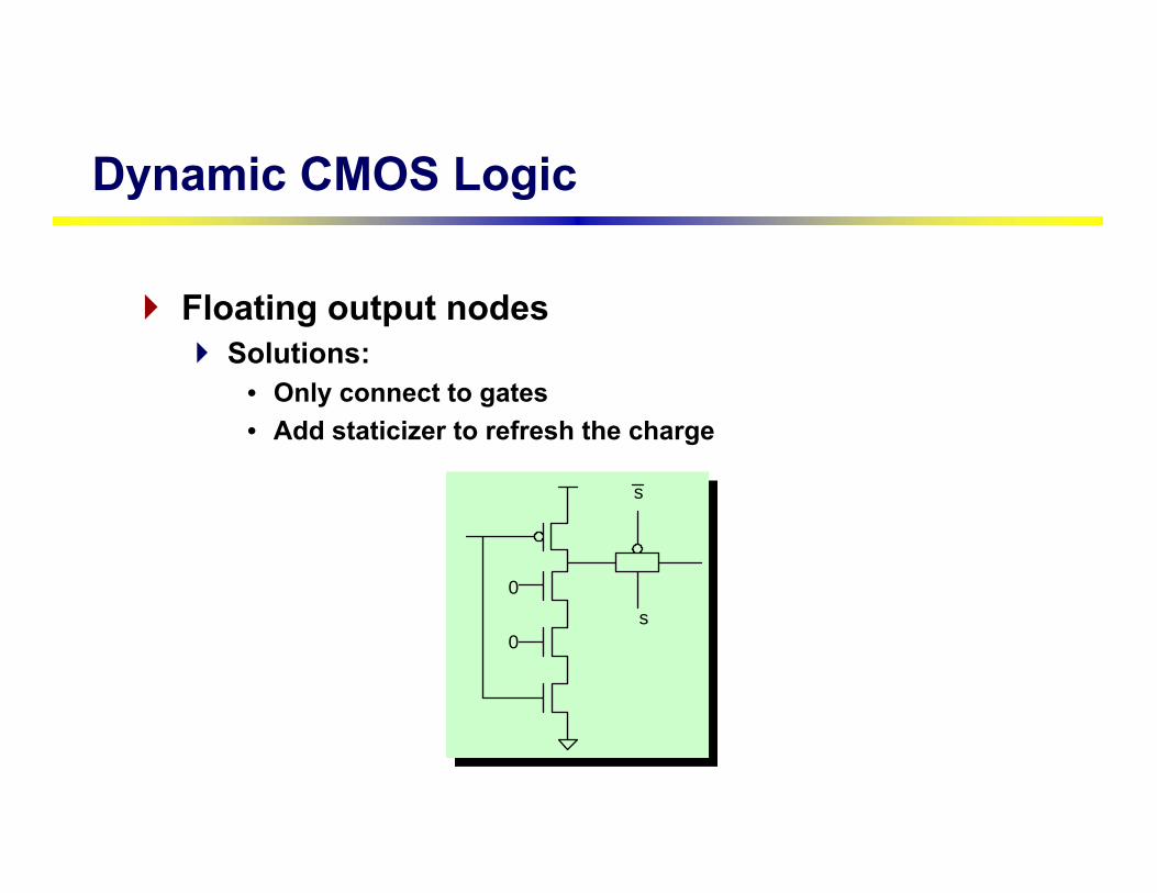
Floating output nodesSolutions:
• Only connect to gates• Add staticizer to refresh the charge
Dynamic CMOS Logic
s
s
0
0
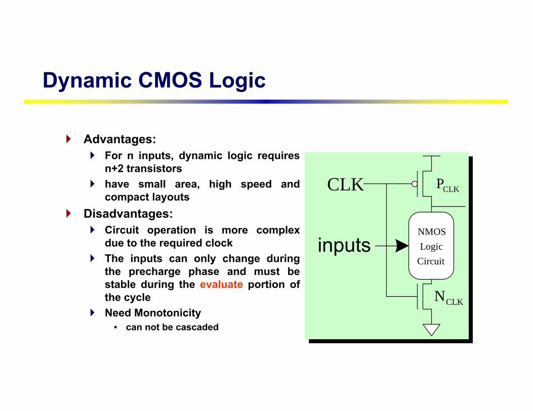
Advantages:For n inputs, dynamic logic requires n+2 transistorshave small area, high speed and compact layouts
Disadvantages:Circuit operation is more complex due to the required clockThe inputs can only change during the precharge phase and must be stable during the evaluate portion of the cycleNeed Monotonicity
• can not be cascaded
Dynamic CMOS Logic
NMOSLogic
Circuit
CLKP
CLKN
CLK
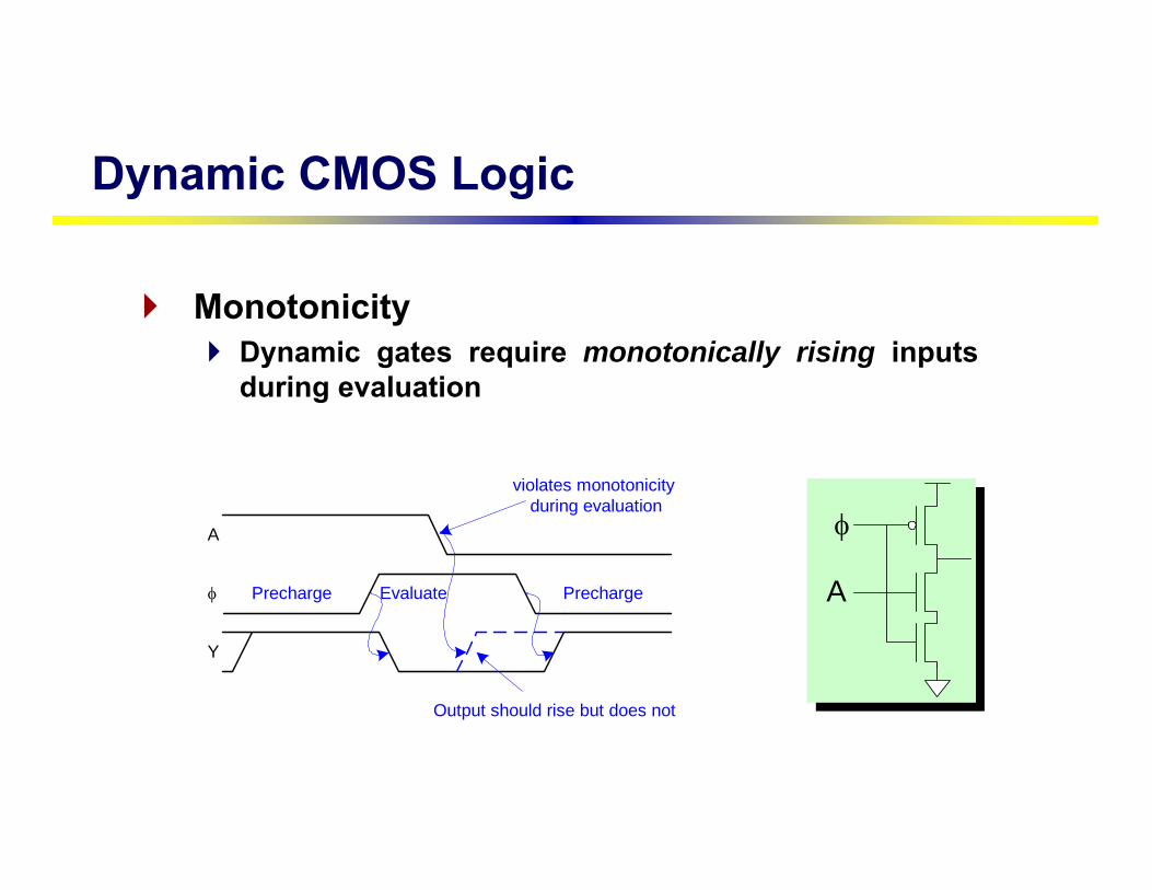
MonotonicityDynamic gates require monotonically rising inputs during evaluation
φ Precharge Evaluate
Y
Precharge
A
Output should rise but does not
violates monotonicity during evaluation
A
φ
Dynamic CMOS Logic
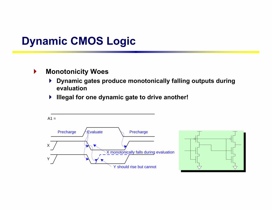
Monotonicity WoesDynamic gates produce monotonically falling outputs during evaluationIllegal for one dynamic gate to drive another!
Dynamic CMOS Logic
Precharge Evaluate
X
Precharge
A = 1
Y should rise but cannot
Y
X monotonically falls during evaluation
V
t
Clk
In
Out1
Out2 ∆V
VTn
Only 0 → 1 transitions allowed at inputs!
Dynamic CMOS Logic
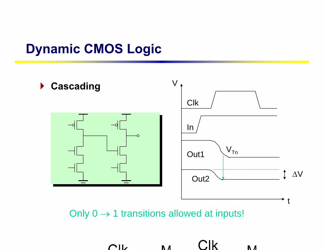
Cascading

CascadingInput going from high to low during evaluation
• a is 5V when precharge b = 5V, c = 5V• During evaluation:
– Wanted: b 0V, c 5V– But, b takes some time to drop to 0V– Consequently, c may fall to some unknown value
SolutionNP-CMOSNORA LogicDomino logic
Dynamic CMOS Logic
a
cb
Dynamic CMOS Logic
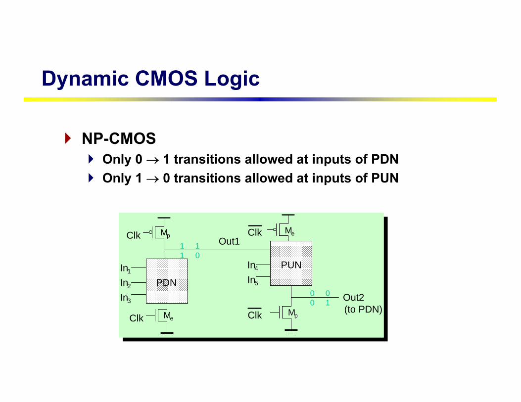
NP-CMOSOnly 0 → 1 transitions allowed at inputs of PDN Only 1 → 0 transitions allowed at inputs of PUN
In1
In2 PDNIn3
Me
Mp
Clk
Clk Out1
In4 PUNIn5
Me
MpClk
Clk
Out2(to PDN)
1 11 0
0 00 1
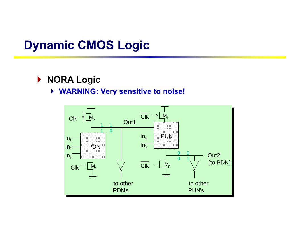
Dynamic CMOS Logic
NORA LogicWARNING: Very sensitive to noise!
In1
In2 PDNIn3
Me
Mp
Clk
Clk Out1
In4 PUNIn5
Me
MpClk
Clk
Out2(to PDN)
1 11 0
0 00 1
to otherPDN’s
to otherPUN’s
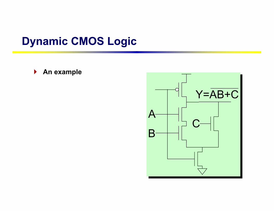
An example
Dynamic CMOS Logic

In1In2In3In4
Out
VDD
GNDφ
Dynamic CMOS Logic
Dynamic 4 Input NAND Gate
1
2
3
e
p
LL
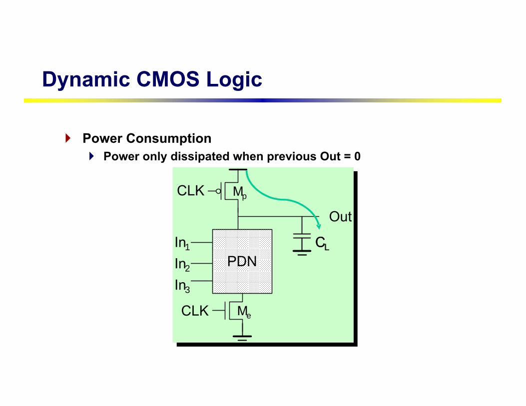
Power ConsumptionPower only dissipated when previous Out = 0
Dynamic CMOS Logic
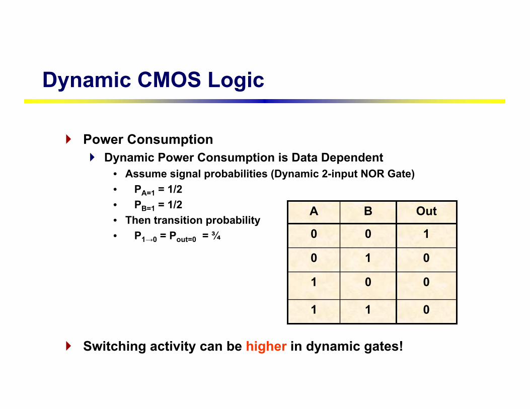
011
001
010
100
OutBA
Power ConsumptionDynamic Power Consumption is Data Dependent
• Assume signal probabilities (Dynamic 2-input NOR Gate)• PA=1 = 1/2• PB=1 = 1/2• Then transition probability• P1→0 = Pout=0 = ¾
Switching activity can be higher in dynamic gates!
Dynamic CMOS Logic

Rules of ThumbDynamic logic is best for wide OR/NOR structure (e.g. bit-lines), providing 50% delay improvement over static CMOSDynamic logic consumes 2x power due to its phase activity (unconditional pre-charging), not counting clock power
Dynamic CMOS Logic
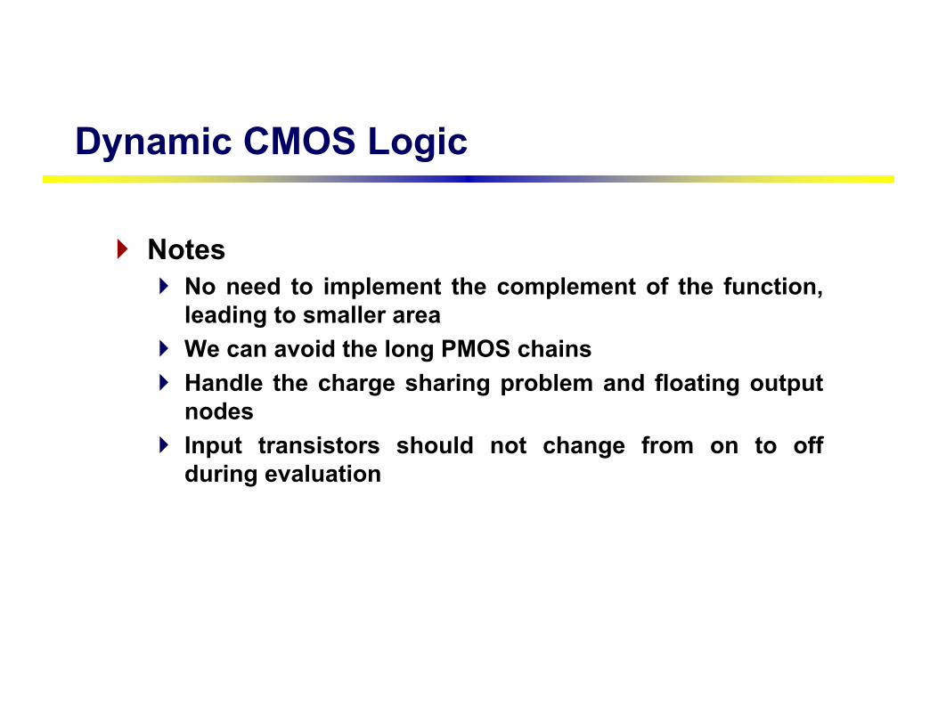
NotesNo need to implement the complement of the function, leading to smaller areaWe can avoid the long PMOS chainsHandle the charge sharing problem and floating output nodesInput transistors should not change from on to off during evaluation
Dynamic CMOS Logic

CMOS Domino Logic
It is an extension of dynamic CMOS gates that allow cascading of stagesThe simple modification entails incorporating a static CMOS inverter at the output of each logic gate
A
W
φ
B C
X Y Z
domino AND
dynamicNAND
staticinverter
In1
In2 PDN
In3
Me
Mp
Clk
ClkOut1
In4PDN
In5
Me
Mp
Clk
ClkOut2
Mkp
1 11 0
0 00 1
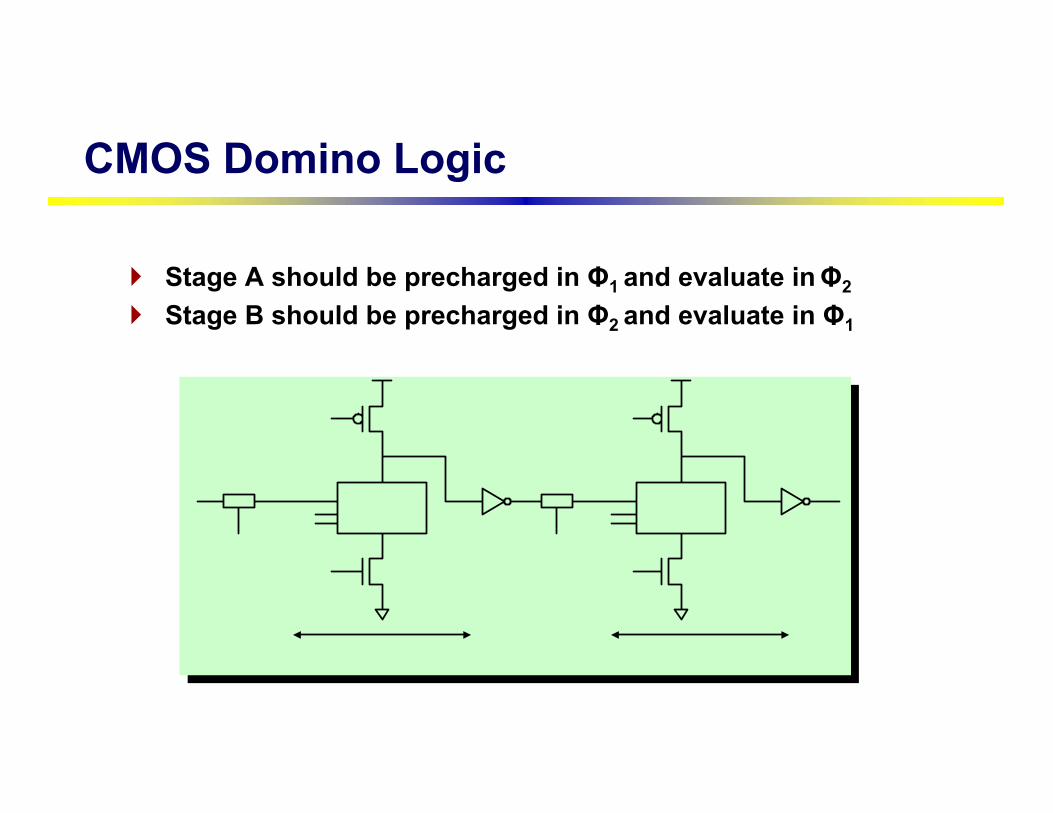
Stage A should be precharged in Φ1 and evaluate inΦ2
Stage B should be precharged in Φ2 and evaluate in Φ1
CMOS Domino Logic

During precharge (clk=0), the output node of the dynamic gate is precharged high and the output node of the CMOS inverter is low. Then subsequent stages will be turned off during the precharge phase
When the clk=1, the output of the driving gate will conditionally discharge, allowing the output of the inverter to conditionally go high. Each connected gate output can then make a transition from low-to-high, in sequence
There is no restriction on the number of logic stages that can be cascaded provided that all stages can evaluate during one clock pulse
CMOS Domino Logic
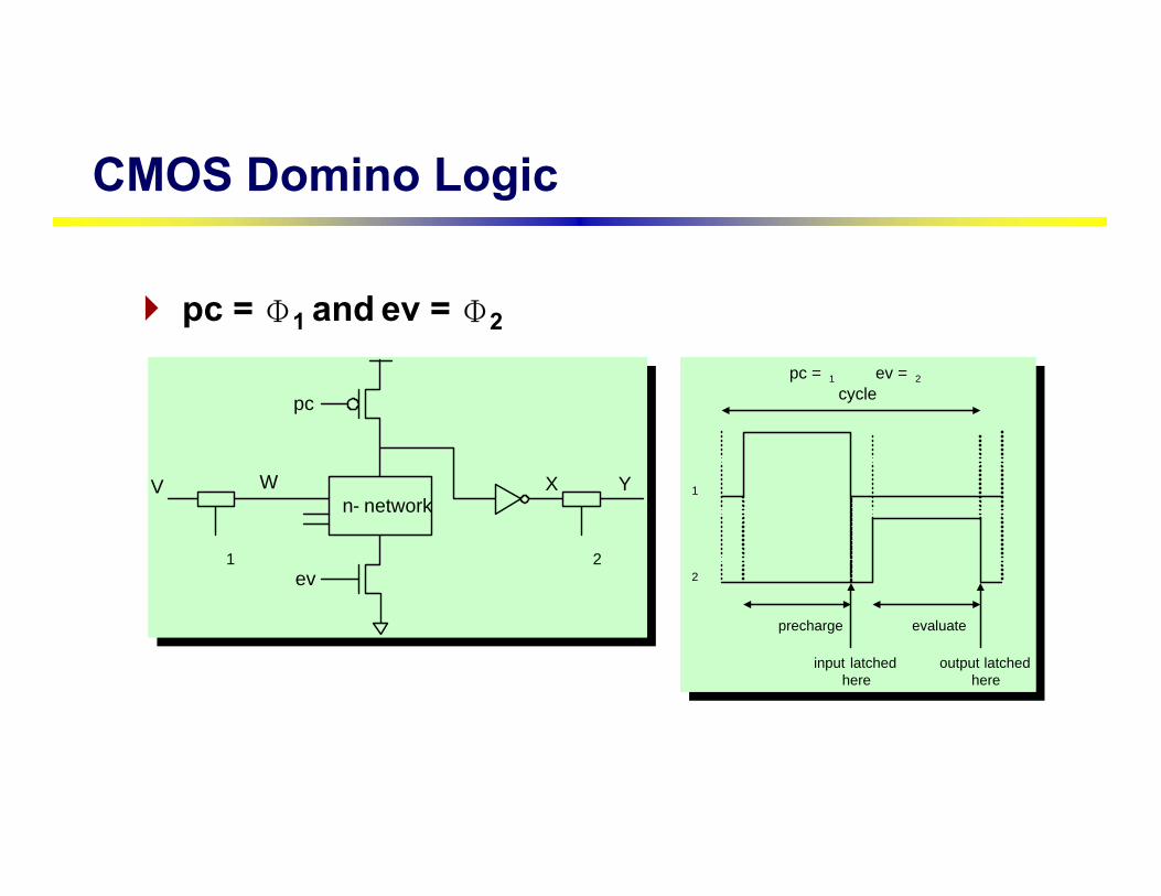
n- network
ev
V
1
W
pc
2
X Y
pc = Φ1 and ev = Φ2
CMOS Domino Logic
cycle
1
2
precharge evaluate
input latchedhere
output latchedhere
pc = 1 ev = 2

Won’t work! If pc = Φ2 and ev = Φ1
CMOS Domino Logic
cycle
1
2
prechargeevaluate
input latchedhere
output latchedhere
pc = 2 ev = 1
evaluate
precharge
CMOS Domino Logic
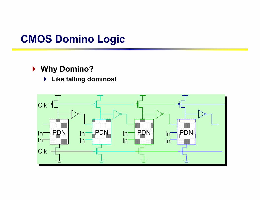
Why Domino?Like falling dominos!

Produces monotonic outputs
φ Precharge Evaluate
W
Precharge
X
Y
Z
A
φ
B C
φ φ φ
C
AB
W X Y Z =X
ZH H
A
W
φ
B C
X Y Z
domino AND
dynamicNAND
staticinverter
CMOS Domino Logic
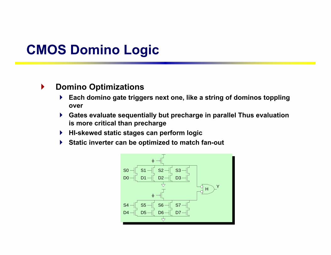
Domino OptimizationsEach domino gate triggers next one, like a string of dominos toppling overGates evaluate sequentially but precharge in parallel Thus evaluation is more critical than prechargeHI-skewed static stages can perform logicStatic inverter can be optimized to match fan-out
S0
D0
S1
D1
S2
D2
S3
D3
φ
S4
D4
S5
D5
S6
D6
S7
D7
φ
YH
CMOS Domino Logic
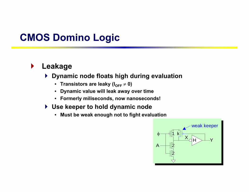
LeakageDynamic node floats high during evaluation
• Transistors are leaky (IOFF ≠ 0)• Dynamic value will leak away over time• Formerly miliseconds, now nanoseconds!
Use keeper to hold dynamic node• Must be weak enough not to fight evaluation
A
φH
2
2
1 kX Y
weak keeper
CMOS Domino Logic
Noise SensitivityDynamic gates are very sensitive to noise• Inputs: VIH ≈ Vtn• Outputs: floating output susceptible noise
Noise sources• Capacitive crosstalk• Charge sharing• Power supply noise• Feedthrough noise• And … !
CMOS Domino Logic
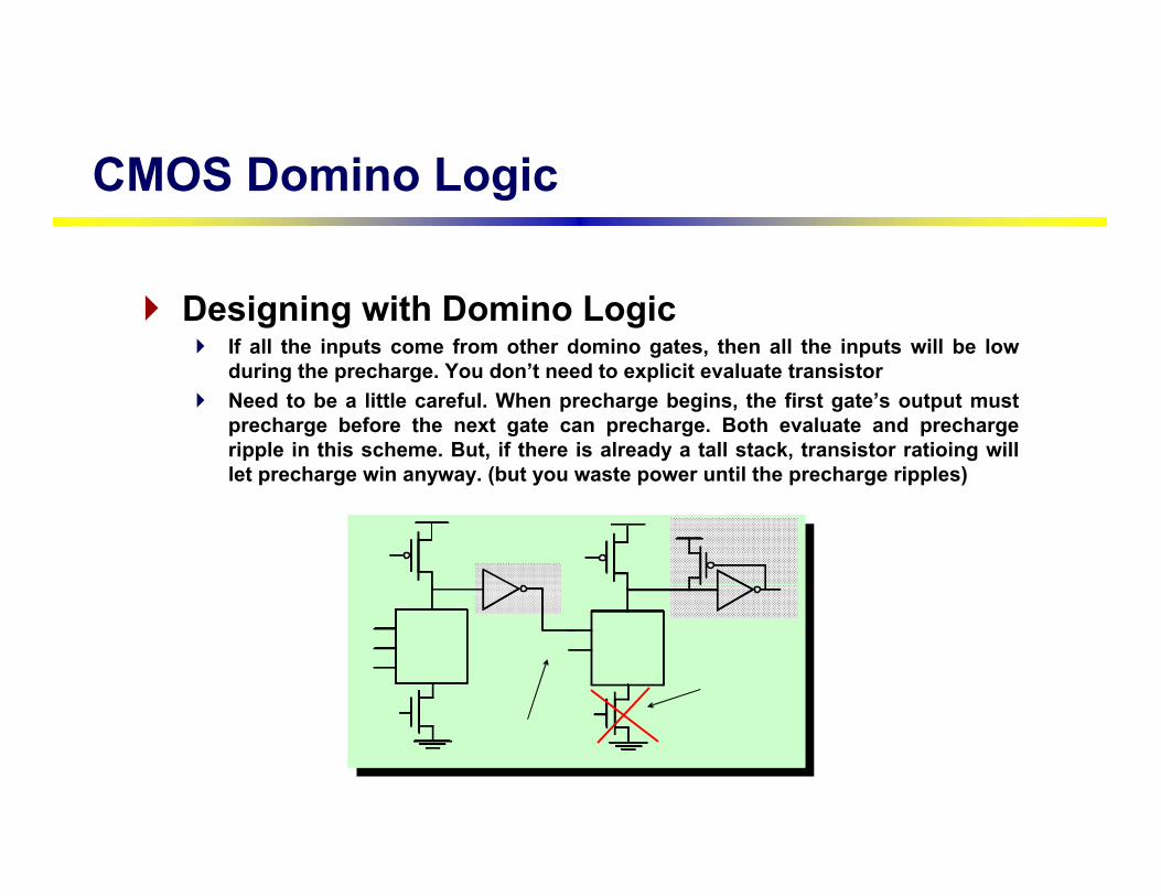
CMOS Domino Logic
Designing with Domino LogicIf all the inputs come from other domino gates, then all the inputs will be low during the precharge. You don’t need to explicit evaluate transistorNeed to be a little careful. When precharge begins, the first gate’s output must precharge before the next gate can precharge. Both evaluate and prechargeripple in this scheme. But, if there is already a tall stack, transistor ratioing will let precharge win anyway. (but you waste power until the precharge ripples)

ExampleDuring precharge, x, y, z = 1, x, y = 0During evaluation, x = 0 when a = b = 1Therefore, z = a b c d
CMOS Domino Logic
a
b
x
c
xy
d
y z
Advantages:Large Fan-in, fewer transistors (n+4 transistors, whereas CMOS requires 2n)Single clock can be used to precharge and evaluate all stages at the same timeIt is attractive for high-speed circuits1.5 – 2x faster than static CMOSWidely used in high-performance microprocessors
Disadvantages:Each logic block must incorporate a separate inverterEach block performs only non-inverting logicMonotonicityLeakageCharge sharingNoise
CMOS Domino Logic
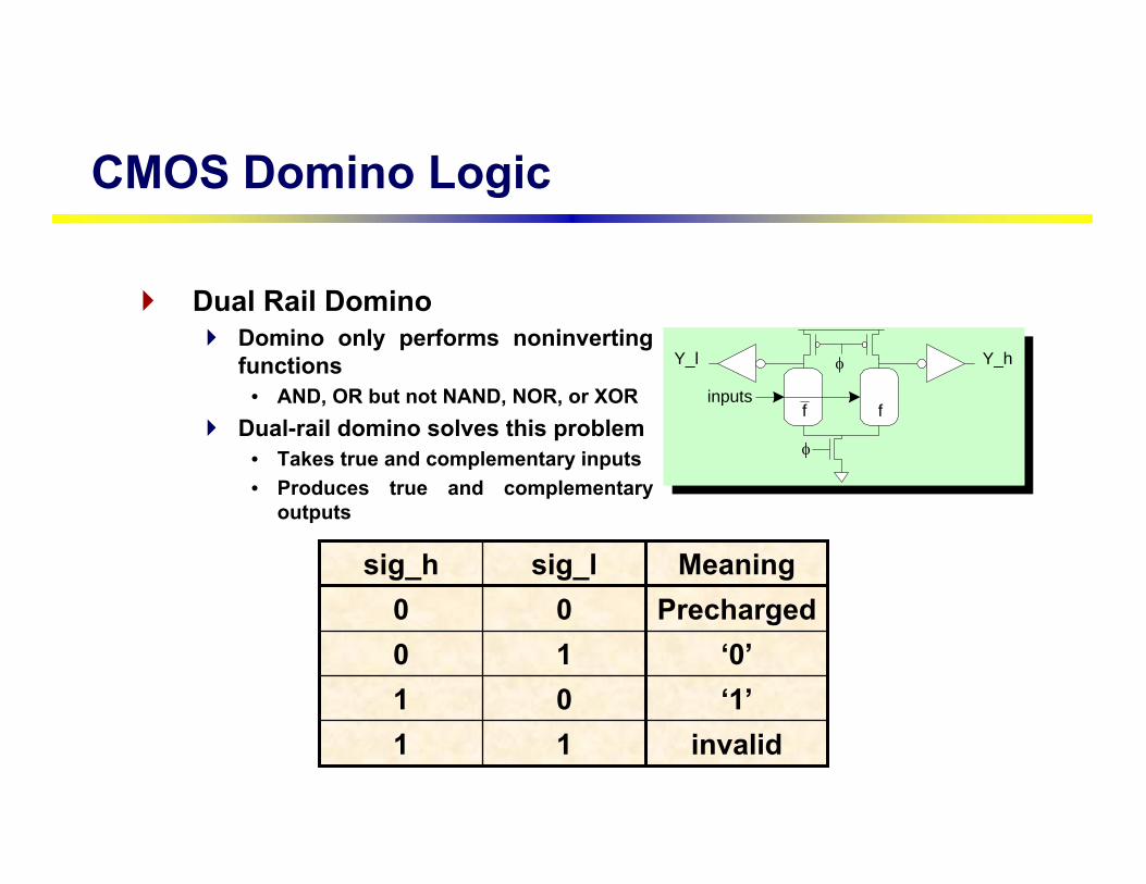
Dual Rail DominoDomino only performs noninverting functions
• AND, OR but not NAND, NOR, or XORDual-rail domino solves this problem
• Takes true and complementary inputs • Produces true and complementary
outputs
invalid11‘1’01‘0’10
Precharged00Meaningsig_lsig_h
Y_h
f
φ
φ
inputs
Y_l
f
CMOS Domino Logic
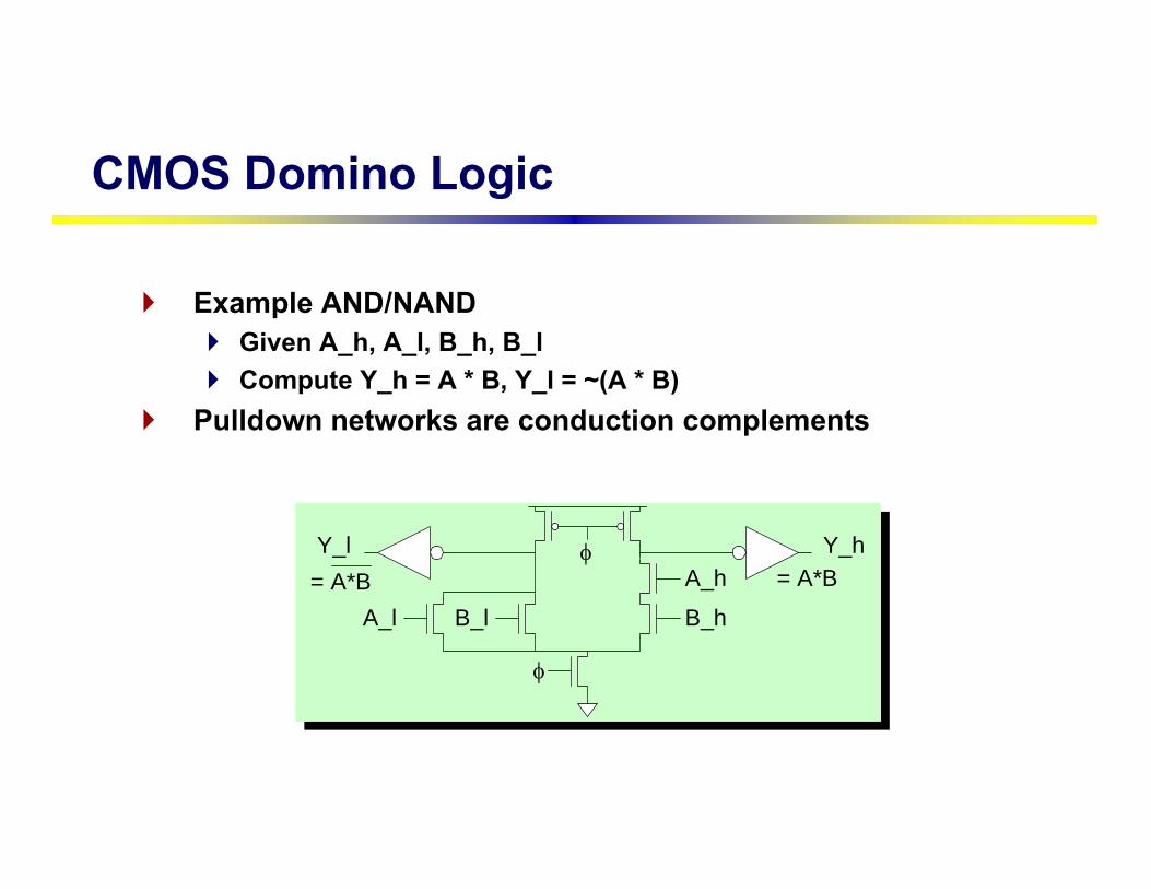
Example AND/NANDGiven A_h, A_l, B_h, B_lCompute Y_h = A * B, Y_l = ~(A * B)
Pulldown networks are conduction complements
CMOS Domino Logic
Y_hφ
φ
Y_lA_h
B_hB_lA_l
= A*B= A*B
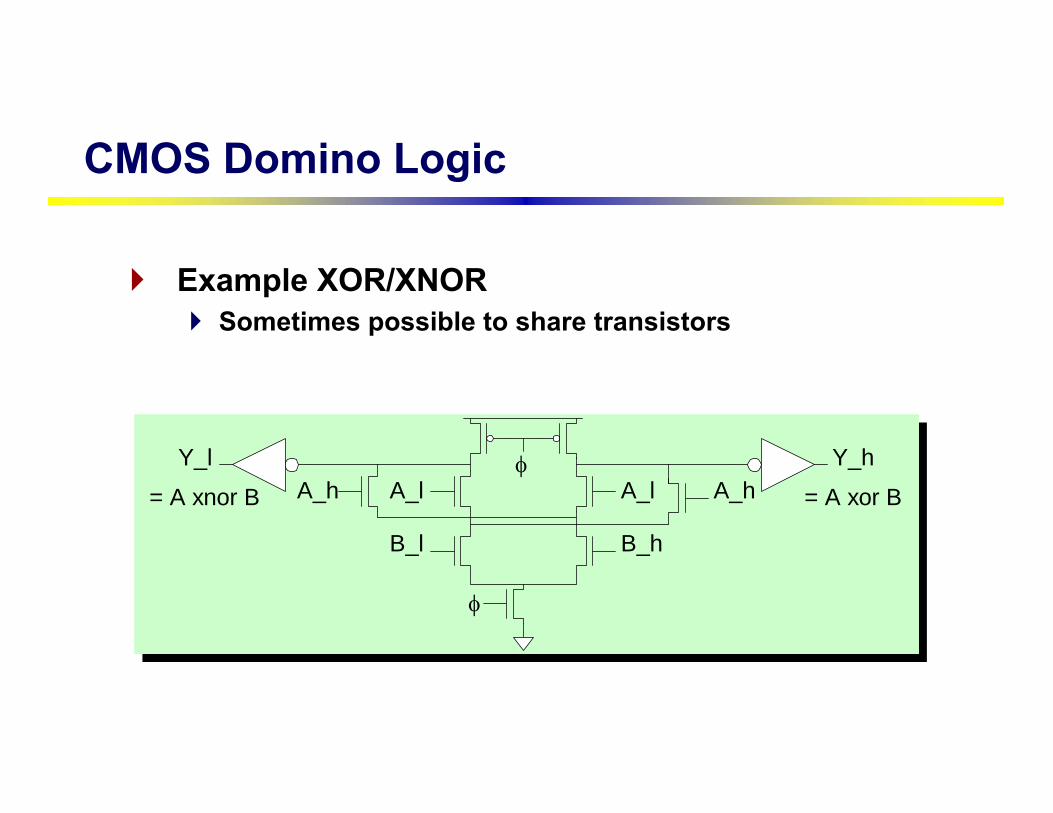
Example XOR/XNORSometimes possible to share transistors
Y_hφ
φ
Y_lA_l
B_h
= A xor B
B_l
A_hA_lA_h= A xnor B
CMOS Domino Logic

Rules of ThumbTypical domino keepers have W/L = 5-20% of effective width of evaluate treeTypical domino output buffers have a beta ratio of ~ 6:1 to push the switch point higher for fast rise-time
CMOS Domino Logic
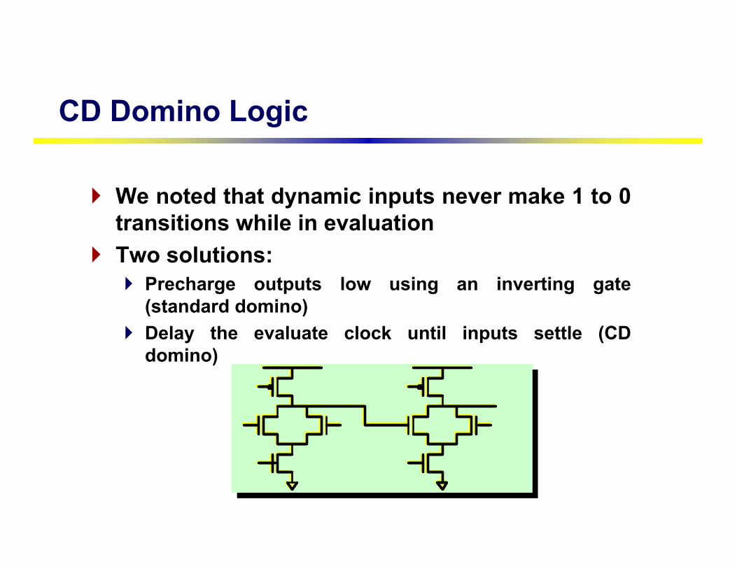
We noted that dynamic inputs never make 1 to 0 transitions while in evaluationTwo solutions:
Precharge outputs low using an inverting gate (standard domino)Delay the evaluate clock until inputs settle (CD domino)
CD Domino Logic
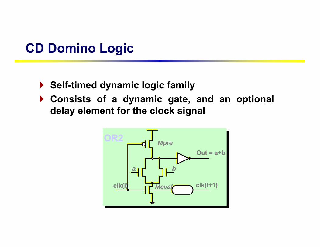
Self-timed dynamic logic familyConsists of a dynamic gate, and an optional delay element for the clock signal
CD Domino Logic
clk(i) clk(i+1)delay
Out = a+bMpre
Meval
a b
clk(i) clk(i+1)delay
Out = a+bMpre
Meval
a b
AdvantagesUses single-rail circuits, rather than dual-rail for standard dominoProvides both inverting and non-inverting functionsHigh-speed, large fan-in NOR and OR circuits
CD Domino Logic
CD Domino Logic
Delay MatchingCD domino requires delay matching between the slowest dynamic gate at a level and a delay elementA 20% margin is typically added to the delay of the fixed delay element to account for PVT variationsThus, 20% of the speed gain possible with CD domino is not realizedAverage speed gain of (60+20)% is theoretically possible
Use digitally programmable delay elements (PDEs) to reduce the margin and attain a speed improvement without affecting the reliability in the presence of variations

Clocking SchemeThe circuits are fully levelizedThe delay element on each level is tuned to the slowest gate at its level, plus a 20% margin
CD Domino Logic
dynamic gate
dynamic gate
dynamic gate
dynamic gate
dynamic gate
dynamic gate
fixed delay fixed delay fixed delay clk1 clk2 clk3 clk4
gate level 1
gate level 3
gate level 2
primary inputs
(other gates)..(other gates)..
(other gates)..dynamic
gate
dynamic gate
dynamic gate
dynamic gate
dynamic gate
dynamic gate
clk1 clk2 clk3 clk4gate level gate level gate level
(other gates)..(other gates)..
(other gates)..(other gates)..
(other gates)..(other gates)..
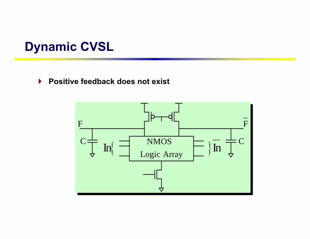
Positive feedback does not exist
Dynamic CVSL
{In }InC
F F
C NMOSLogic Array
It is one type of Dynamic CVSL with positive feedbackBy this logic the low level output is guaranteed to zero in evaluation phase
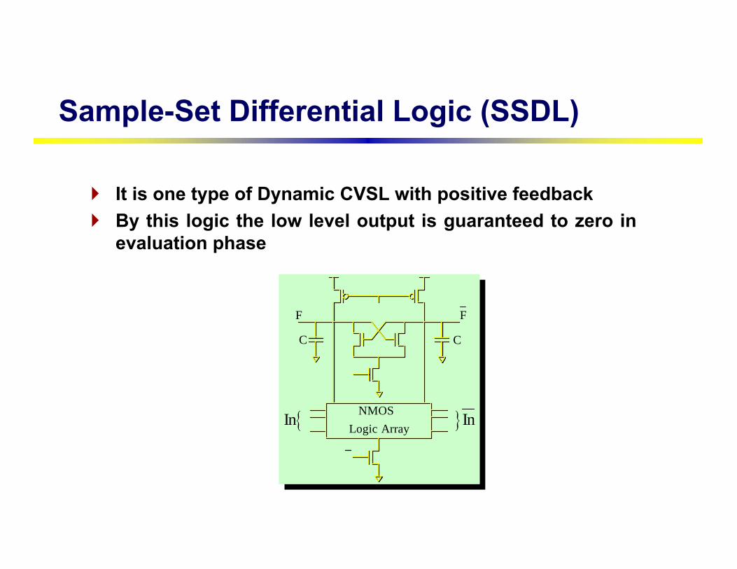
Sample-Set Differential Logic (SSDL)
{In }In
C
F F
C
NMOSLogic Array
Summary
This lecture describes many basics CMOS Logic Gates which require clock or other periodic signal for operation These circuits rely on the temporary storage of signal values on the (parasitic) capacitance of high impedance nodes