mosfet driver with protection and diagnostic
TRANSCRIPT

Automotive IPS
MOSFET Driver AUIR3200S
1 Rev 1.1 2016-05-2
Automotive grade
MOSFET DRIVER WITH PROTECTION AND DIAGNOSTIC
Features Bootstrap and charge pump Over temperature shutdown (with Ptc interface) Short circuit protection (Vds detection) Reverse battery protection (turns On the MOSFET) Ground loss protection Diagnostic
ESD protection
Description The AUIR3200S is a high side mosfet driver for very low Rdson automotive application. It offers over-current, over-temperature protection and diagnostic. The over-current protection is done by monitoring the Vds voltage, the threshold is programmable by external resistor. The over-temperature protection uses a thermal sensor. The AUIR3200S offers diagnostic on the input pin.
Product Summary
Operating voltage 6-36V Vgate 6V
Package
SO8
Ordering Information
Base Part Number Package Type Standard Pack
Complete Part Number Form Quantity
AUIR3200S SOIC-8 leads Tape and Reel 2500 AUIR3200STR

AUIR3200S
2 Rev 1.1 2016-05-02
Typical Connection
Cboot
Load
+Bat
Input Signal V Diag
Rdiag
G
S In/Dg
Gnd
Vcc
Ptc
Vds
Rin
Rvds
Ptc sensor
AUIR3200S
Rgate
MOSFET Logic level
100nF

AUIR3200S
3 Rev 1.1 2016-05-02
Absolute Maximum Ratings Absolute maximum ratings indicate sustained limits beyond which damage to the device may occur. All voltage parameters are referenced to Ground lead. (Tj= -40°C..150°C unless otherwise specified).
Symbol Parameter Min. Max. Units Vcc-gnd Maximum Vcc voltage -0.3 60
V
Vcc-Vds Maximum Vds pin voltage -0.3 5.5
Vcc-Vptc Maximum Ptc pin voltage -0.3 5.5
Vin-gnd Maximum IN pin voltage -0.3 5.5
Vcc-Vs Maximum S pin voltage -0.3 60
Vcboot-Vs Maximum Cboot pin voltage -0.3 8
Vcc cont. Maximum continuous Vcc voltage 36
Tj max. Maximum operating junction temperature -40 150
°C Maximum storage temperature -55 150
Tsoldering Soldering temperature (10 seconds) 300
Thermal Characteristics
Symbol Parameter Typ. Max. Units Rth Thermal resistance junction to ambient 100 °C/W
Recommended Operating Conditions
Symbol Parameter Min. Max. Units VIH High level input voltage 2.7 5.5
V VIL Low level input voltage 0 0.9
Rin Recommended resistor in series with IN pin 10 15
k Rdiag Recommended resistor in series with Diag pin 4 15
Rvds Maximum recommended Rvds, see page 7 2.9

AUIR3200S
4 Rev 1.1 2016-05-02
Static Electrical Characteristics Tj=-40°C..125°C, Vcc=6-36V (unless otherwise specified), typical value are given for Vcc=14V and Tj=25°C.
Symbol Parameter Min. Typ. Max. Units Test Conditions Vcc op. Operating voltage range 6 36 V
Icc Off Supply current in sleep mode Tj=25°C 1 5 µA Vcc=14V, Vin=0V
Icc On Supply current when On 10 15 mA Vin=5V, Vptc=Vbat, Vds=Vbat
VIH IN High threshold voltage 2 2.6
V
VIL IN Low threshold voltage 0.5 1.7 2.1
In hyst. Input hysteresis 0.2 0.5 1
Iin on On state input current 33 50 µA Vin=5V
Vgs Gate output voltage 5 5.7 7
V
Igs=0µA
Vgs rev Gate output voltage during reverse battery Tj=25°C
4.5 5.6 7 Igs=50µA, Vbat=14V
Vin, off Input voltage when the part is in fault mode
0.25 0.4 Idg=300µA
Protection Characteristics Tj=-40°C..125°C, Vcc=6-36V (unless otherwise specified), typical value are given for Vcc=14V and Tj=25°C.
Symbol Parameter Min. Typ. Max. Units Test Conditions
Ivds Vds current reference
0.7 0.8 0.91
mA
Vcc-Vds=0V, Tj=-40°C
0.84 0.93 1.05 Vcc-Vds=0V, Tj=25°C
1 1.15 1.33 Vcc-Vds=0V, Tj=125°C
Vds offset Vds comparator offset -10 0 10 mV
Tblank on Vds detection blanking time during turn on
15 22 35 µs
Tdiag Diagnostic time 10
ms see figure 6 Tsleep Time to enter in sleep mode 7 15 30
Treset Time to enter in sleep mode and reset the fault
5
Twkp Time to leave the sleep mode 0.5 µs
Rin=10k see figure 7 &8
Tpwr on rst Power on reset duration Tj=25°C 40 100 200
UV Under voltage threshold 5.2 5.9 V
T UV hold Time to keep UV detection active 150 350 600 µs
Ptc_sensor Ptc sensor threshold value when over temperature
1.3 5 14.3
k
see page 2 & 8
Rptc Pull down resistor on the PTC pin 4 10 20 Buit-in resistor See page 6
Vptc PTC comparator voltage threshold (Vcc-Vptc)
1.5 2 2.5 V Vin=5V, Vcc=14V

AUIR3200S
5 Rev 1.1 2016-05-02
Switching Characteristics Tj=-40..125°C, Vcc=6..36V (unless otherwise specified), typical value are given for Vcc=14V and Tj=25°C.
Symbol Parameter Min. Typ. Max. Units Test Conditions Tdon Turn-on delay to 20% of Vgs 1.6
µs Qg=220nc,
Rgate=0
Tr Rise time 20% to 80% of Vgs 1
Tdoff Turn off delay time to 80% of Vgs 2
Tf Fall time from 80% to 20% of Vgs 1
Igs+ Gate output high pulsed current 100 160 mA
Vgs=0V
Igs- Gate output low pulsed current 100 130 Vgs=5.7V
Iboot Cboot capacitor charge current 0.35 0.8 A
Vboot-Source Cboot capacitor charge voltage 5.6 6 V
True Table
Operating Conditions IN OUT DG Normal ON H H H
Normal OFF L L L
Short circuit to Gnd H L L
Short circuit to Gnd L L L
Over-temperature H L L
Over-temperature L L L

AUIR3200S
6 Rev 1.1 2016-05-02
Lead Assignments
Functional Block Diagram All values are typical
+
-
75V
Boot strap regulator
11V
6V
6V 6V 1mA
Level
Shifter
+
-
Vcc-6V
Vcc-6V
Vptc=Vcc-2V
UV 4 clk
Counter
t Blanking
ON
Rptc
IN/DG
VCC
15
0k
Charge
Pump
2V
1.7V
6V
GND
75V
PTC Vds
G
S
Cboot
S
R
Q
Q
Diagnostic Sleep mode
10
0
10
k
Driver

AUIR3200S
7 Rev 1.1 2016-05-02
Over-current protection The over-current protection is done by monitoring the Vds voltage of the Mosfet. The threshold is adjusted by connecting the appropriate resistor between Vcc and Vds pin => Rvds. Below the formula to set the appropriate over-current threshold:
_Ivds Rvds
Isd thresholdRdsOn
We advise to you to take low tolerance resistor for Rvds for optimize the precision of your current level protection. The AUIR3200S doesn’t have feedback of the Mosfet temperature. We take in the consideration that Tcase of AUIR3200S will be almost the same like the Tcase of Mosfet. The current Ivds has a positive temperature coefficient to compensate the positive temperature coefficient of the Rdson of the Mosfet. The above formula is only valid when the Mosfet is fully ON. Therefore during the turn on of the MOSFET, the time ‘Tblank on’ disables the vds protection until the Mosfet is fully On. Therefore a maximum resistor is specified for Rvds in the recommended section. With a higher resistor, the part will latch.
Figure 1: Protection Vds
t
Vin (V)
Iout (A)
Vds (V)
Over-current shutdown
Vdiag (V)
Vds > Vrvds
V Rvds (V)
0
0
0
0
t
t
t
Vds threshold

AUIR3200S
8 Rev 1.1 2016-05-02
Over-temperature protection The temperature protection uses a PTC sensor connected to the tab or the drain of the Mosfet depending on the mounting. This sensor will increase with the temperature. When his value is above 5kΩ (typical value) the protection will be activated.
VPTC > 2V when the RPTC > 5kΩ:
Figure 2: Protection PTC
For optimize the precision of the protection it is important to maximize the thermal interface between the sensor and the junction. The PTC sensor needs to be placed the closest possible of the MOSFET and to be surrounded by copper. The connection with AUIR3200S could be doing by a trace in bottom side of the PCB.
Figure 3: Layout example (top side)
Vin (V)
Iout (A)
Tj (°C)
Over-temperature shutdown
Vdiag (V)
Vcc - Vptc (V) 2V (typ.)
t
t
t
t 0
0
0
0
0 t
MOSFET
PTC sensor
Copper plan

AUIR3200S
9 Rev 1.1 2016-05-02
The PTC protection could be activated if PTC sensor is higher than 1.3kΩ (see page 4: ‘Ptc sensor’ characteristic).
Figure 4: Typical PTC curve (Rptc vs Temperature)
In this area the PTC protection
could be activated
PTC sensor<1.3kΩ: no activation
possible of PTC protection

AUIR3200S
10 Rev 1.1 2016-05-02
Protection evaluation The PTC sensor, the Vds threshold and the Mosfet must be chosen in order to not exceed the maximum junction temperature of the Mosfet during a short circuit. Protection is evaluated by switching the Mosfet on different currents and by evaluating the junction temperature when the Mosfet is switched off by the protections. This evaluation gives the following drawing.
- For high impedance short circuit, Vds is smaller than Vds threshold, so the over-temperature will act. - For low impedance short circuit, the Vds protection will switch off the Mosfet.
At the transition current between the 2 protections the junction temperature of the Mosfet is the maximum and should be lower than the maximum rating.
Figure 5: Protection evaluation
Maximum Tj of your system. Need to be lower than Tj max of the mosfet.
Ju
nc
tio
n t
em
pe
ratu
re a
t sw
itch
off
Short-circuit current
Over-temperature protection
Over-current protection

AUIR3200S
11 Rev 1.1 2016-05-02
Sleep_mode / Diagnostic Sleep_mode block manages the diagnostic and the sleep_mode. The device enters in sleep mode if input is inactive during a delay higher than Tsleep.
IN
diag internal
diag
out
tdiag
tdiag
sleep mode Fault mode Normal mode
treset
tsleep
Figure 6
Wake up sequence To wake up the part from the sleep mode, the input must be activated at least during Twkp, then the bootstrap regulator is switched on and the bootstrap capacitor is charged. The output will not be activated during Tpw on rst.
IN
out
sleep mode Normal mode
tpw on rst
twkp
tsleep
sleep mode
Figure 7
IN
out
sleep mode Normal mode
tpw on rst
twkp
Figure 8
AUIR3200S
12 Rev 1.1 2016-05-02
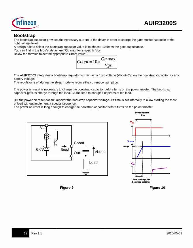
Bootstrap The bootstrap capacitor provides the necessary current to the driver in order to charge the gate mosfet capacitor to the right voltage level. A design rule to select the bootstrap capacitor value is to choose 10 times the gate capacitance. You can find in the Mosfet datasheet ‘Qg max’ for a specific Vgs. Below the formula to set the appropriate Cboot value:
max10
QgCboot
Vgs
The AUIR3200S integrates a bootstrap regulator to maintain a fixed voltage (Vboot=6V) on the bootstrap capacitor for any battery voltage. The regulator is off during the sleep mode to reduce the current consumption. The power on reset is necessary to charge the bootstrap capacitor before turns on the power mosfet. The bootstrap capacitor gets its charge through the load. So the time to charge it depends of the load. But the power on reset doesn’t monitor the bootstrap capacitor voltage. Its time is set internally to allow starting the most of load without implement a special sequence: The power on reset is long enough to charge the bootstrap capacitor before turns on the power mosfet.
Cboot
Vcc
Out 6.6V
Load
Iboot Vboot
Figure 9 Figure 10
charged
V in
V g
Power on reset time
Time to charge the bootstrap capacitor
charged
V in
V gs
Power on reset time
Time to charge the bootstrap capacitor
V boot

AUIR3200S
13 Rev 1.1 2016-05-02
If the inductance of the load is too important, the power on reset is not enough long to charge completely the bootstrap capacitor before turns on the power mosfet. So the micro-processor need to implement a special sequence to start the device without activates the output power mosfet. The micro-processor send one short pulse (Twkp max < short pulse < Tpwr_on_rst min) then wait for the bootstrap capacitor is totally charged and after provide the appropriate duty cycle. The bootstrap charge depends of the battery voltage, the bootstrap capacitor value and the inductance load value.
Figure 11
charged
V boot
V in
V g
Power on reset time
Time to charge the bootstrap capacitor
charged
V
V in
V gs
Power on reset time
Time to charge the bootstrap capacitor
Twake min

AUIR3200S
14 Rev 1.1 2016-05-02
IN frequency and duty cycle The Vds protection is not active if the time ON is lower than Tblank on. So the minimum time ON (ton) is ‘Tblank on max’ to be sure that this protection will be active. The times OFF (toff) needs to be setup for assure that the capacitor bootstrap will be recharged up to 6V. The bootstrap time charge depends of the bootstrap capacitor value and the inductance load value.
Figure 12
If the capacitor is discharged at the turn ON of the MOSFET, the AUIR3200S will detect a fault (VDS protection) after Tblank ON because the MOSFET won’t be fully ON.
Figure 13
Vds threshold
ton
toff IN
Vboot
Vdiag
Normal mode
0V
Vds
MOSFET
0V
6V
Tblank On Tblank On
IN
Vboot
Vdiag
Fault mode Normal mode
0V
Vds
MOSFET
0V
VDS threshold
VDS > VDS threshold

AUIR3200S
15 Rev 1.1 2016-05-02
Under voltage protection in short-circuit mode During short circuit condition, it may happen that the supply voltage drops below the under voltage before the short is detected by the Vds protection due to the blanking time ‘Tblank on’. In under voltage condition the AUIR3200S turns off the MOSFET. The time ‘Tblank On’ is reset.
Figure 14
In order to detect the short circuit condition, the AUIR3200S has a counter and after 4 ‘under voltage’ detections, the part is latched and the fault diagnostic is activated. The counter is reset when the part goes to sleep mode.
Figure 15
IN
Vcc
UV
0V
Vds
MOSFET
0V
Tblank On
T UV hold
Tblank On
IN
Vcc
Vdiag
sleep mode Fault mode Normal mode
UV
0V
Vds
MOSFET
0V

AUIR3200S
16 Rev 1.1 2016-05-02
PWM operation ( Ton<Tblank on) PWM operation is also possible. The boostrap feature allows fast switching. When the Ton is shorter than the Tblank On, the Vds protection is no longer activated. In order to protect the Power Mosfet, the AUIR3200S integrates a counter which is incremented by the input signal and reset when the Vds voltage is below the Vds threshold. The counter latches off the AUIR3200S after 4 activations. During PWM operation ( Ton< Tblank On) on a short circuit, the Vds is always above the Vds threshold and 4 activations on the input will latch the AUIR3200S and the fault diagnostic is activated.
Figure 16
IN
Vdiag
Fault mode Normal mode
Vds th
Vds
MOSFET
0V
1 2 3 4
<Tblank On

AUIR3200S
17 Rev 1.1 2016-05-02
Tj, junction temperature (°C)
Figure 17: Icc off (µA) Vs Tj (°C) (Vcc=14V,Vin=0V)
Icc o
ff, supply
le
akage c
urr
ent (µ
A)
Tj, junction temperature (°C)
Vih
and V
il (V
)
Figure 18: Vih and Vil (V) Vs Tj (°C)
0.0
0.2
0.4
0.6
0.8
1.0
1.2
1.4
1.6
1.8
2.0
-40 10 60 110
0
1
2
3
4
5
6
7
0 10 20 30
Vcc, operating voltage (V)
Vgs,
outp
ut
gate
voltage (
V)
Figure 19: Vgs vs Vcc with Ivgs=50µA
0.0
0.5
1.0
1.5
2.0
2.5
-40 -20 0 20 40 60 80 100 120 140
Vih
Vil
Parameters curves: typical value

AUIR3200S
18 Rev 1.1 2016-05-02
Case Outline – SO8

AUIR3200S
19 Rev 1.1 2016-05-02
Tape & Reel SO8

AUIR3200S
20 Rev 1.1 2016-05-02
Part Marking Information
Qualification Information†
Qualification Level
Automotive (per AEC-Q100)
Comments: This family of ICs has passed an Automotive qualification. IR’s Industrial and Consumer qualification level is granted by extension of the higher Automotive level.
Moisture Sensitivity Level SOIC8N MSL2
260°C
(per IPC/JEDEC J-STD-020)
ESD
Machine Model Class M1B(+/-100V) (per AEC-Q100-003)
Human Body Model Class H1C (+/-1500V) (per AEC-Q100-002)
Charged Device Model Class C4 (+/-1000V) (per AEC-Q100-011)
IC Latch-Up Test Class II, Level A
(per AEC-Q100-004)
RoHS Compliant Yes
† Qualification standards can be found at International Rectifier’s web site http://www.irf.com/

AUIR3200S
21 Rev 1.1 2016-05-02
Published by Infineon Technologies AG 81726 München, Germany
© Infineon Technologies AG 2015
All Rights Reserved. IMPORTANT NOTICE The information given in this document shall in no event be regarded as a guarantee of conditions or characteristics (“Beschaffenheitsgarantie”). With respect to any examples, hints or any typical values stated herein and/or any information regarding the application of the product, Infineon Technologies hereby disclaims any and all warranties and liabilities of any kind, including without limitation warranties of non-infringement of intellectual property rights of any third party. In addition, any information given in this document is subject to customer’s compliance with its obligations stated in this document and any applicable legal requirements, norms and standards concerning customer’s products and any use of the product of Infineon Technologies in customer’s applications. The data contained in this document is exclusively intended for technically trained staff. It is the responsibility of customer’s technical departments to evaluate the suitability of the product for the intended application and the completeness of the product information given in this document with respect to such application. For further information on the product, technology, delivery terms and conditions and prices please contact your nearest Infineon Technologies office (www.infineon.com). WARNINGS
Due to technical requirements products may contain dangerous substances. For information on the types in question please contact your nearest Infineon Technologies office. Except as otherwise explicitly approved by Infineon Technologies in a written document signed by authorized representatives of Infineon Technologies, Infineon Technologies’ products may not be used in any applications where a failure of the product or any consequences of the use thereof can reasonably be expected to result in personal injury.

AUIR3200S
22 Rev 1.1 2016-05-02
Revision History Revision Date Notes/Changes
A November, 2nd 2012 Initial release
B January, 3rd 2013 Add max Rvds
D April, 24th 2015 Add ‘Rptc sensor’ parameter Add explanation for current protection and temperature protection
E1 June, 3 th 2015 Add Vgs max and Vgs rev max
E3 September, 24 th 2015
IFX template
E4 October, 2 2015 Twkp max added
1.1 May 02, 2016 Ground loss protection Update revision name