mosfet scaling - rice universityphys533/notes/week09_lectures.pdf · mosfet scaling • can we just...
TRANSCRIPT

1
MOSFET scaling
• Can we just keep miniaturizing conventional FETs?
No - new physical effects kick in at small length scales. Not all these effects are bad, but certainly make design more complicated. Some can be mitigated by particular scaling schemes.
• What kind of variations on CMOS are proposed, and why?
• How far can these variations take us - when does it become essential to change to a new architecture based on new operating principles?
What happens in smaller transistors?
If we simply shrink all length scales, a number of physical effects can become relevant that are unimportant in larger MOSFETs:
• Channel shortening
• “Punch-through”
• Tunneling / thermionic leakage
• Threshold voltage variation with drain bias
• Finite width effects
• Velocity saturation
• Field-dependent mobility
• Avalanche breakdown
• Oxide failure

2
Where is all the action?
We derived transistor characteristics (e.g. square law) by looking at the charge in this box area under the gate.
“Gate Charge Approximation” (GCA): assumes that charge distribution in that box is dominated by effects from gate field. That is, for electric fields in that region.xy FF >>
Anything that affects charge distribution in or very near this box will produce changes away from our simple model predictions….
Channel shortening
First example happens when VD approaches (VG-VT). In long channel devices, we get pinchoff and saturation of ID:
L-∆L ∆L
In really short devices, ∆L can be a significant fraction of L!
What happens then?
Remember, Fx is large over ∆L - that’s where most of the source-drain voltage is dropped.
While inversion layer is gone, drift is enhanced by high electric field there: result is a boost in ID as VD is increased beyond Vdsat.

3
Channel shortening
( )DD
DTGx
D VV
VVVL
CWI λµ + −−= 1
2)(
2
Semiempirical formula based on square law picture:
( )DDTGx
Dsat VVVV
L
CWI λµ + −≈ 1
2
)( 2
• No true saturation.
• Can even have problems at gate voltages that should be below threshold!
Punch-throughIn sufficiently small devices, the depletion regions from the source and drain can actually merge.
This is particularly awkward since the drain depletion region is strongly altered by VD.
• Gate only influences small volume near surface.
• Current can flow through depletion zone - “space-charge-limited” ~ VD
2.
• How to mitigate? Higher doping concentration in bulk wafer leads to shorter depletion widths, though there is an upper limit to reasonable doping.

4
Tunneling / thermionic leakage
Consider an n-MOSFET below threshold, but with a finite source-drain bias.
Plot the energy of the conduction band as a function of position along the channel.
decreasingdevice length, increasing bias.
“Drain-Induced Barrier Lowering” (DIBL).
Thermionic leakage / tunneling
• Both processes can be relevant.
• Tunneling matters more for smaller devices; thermionic emission matters more for higher temperatures.
• Biggest problem is that these can lead to substantial off-currents and power dissipation!

5
Threshold voltage variation
Consider electrostatic potential contours as devices are shortened.
For fixed VG, shorter channel means φ more dominated by VD, just from geometry.
Result: Apparent VT can be quite different in short devices!
Trends:• Shorter channel = lower threshold voltage• Higher VD = lower threshold voltage.• Thinner oxide = higher threshold voltage.
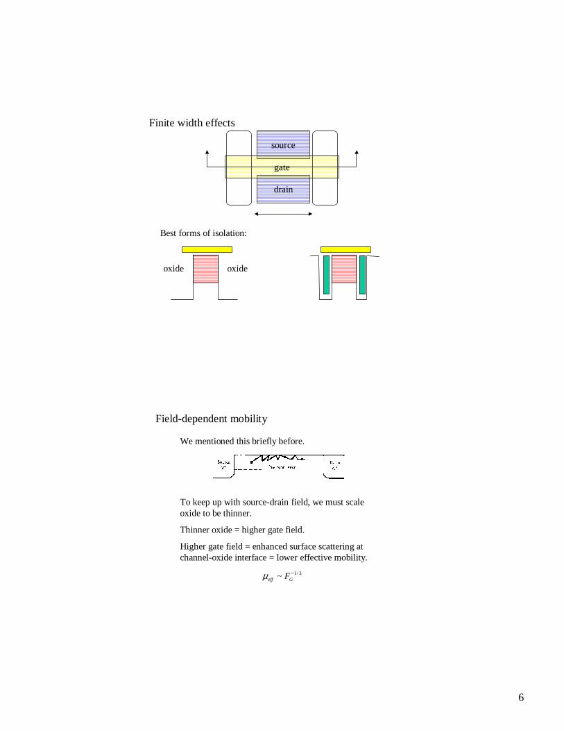
Finite width effects
Top view of MOSFET:
source
drain
gate
W
Some kind of isolation, to prevent gate from affecting more semiconductor than desired.
As overall devices shrink, isolation becomes increasingly important to avoid “parasitic” effects.
6
Finite width effects
source
drain
gate
Best forms of isolation:
oxide oxide
Field-dependent mobility
We mentioned this briefly before.
To keep up with source-drain field, we must scale oxide to be thinner.
Thinner oxide = higher gate field.
Higher gate field = enhanced surface scattering at channel-oxide interface = lower effective mobility.
3/1~ −Geff Fµ

7
Velocity saturation
Electric fields can get quite large in short channel devices.
Does our simple mobility picture still work?
• No: if velocity of carriers becomes large enough, they can lose energy by inelastic processes (e.g. shedding optical phonons).
• If L is long compared to the inelastic scattering length, one sees velocity saturation:
satTGxDsat vVVWCI )( −→
Results:
• This is a significant reduction in current.
• Saturation current now depends linearly on VG-VT rather than almost quadratically.
Velocity saturation
Some example numbers:
Si, 300 K vsat ~ 107 cm/s
when Fx > ~ 3 x 10⁴ V/cm for electrons,
when Fx > ~ 105 V/cm for holes.
real data model with vsat model with novsat

8
Velocity overshoot
What happens if channel is shorter than inelastic scattering length?
• Velocity overshoot: can get channel velocities higher than what would be expected for simple equilibrium transport
• Result can be odd features in transistor characteristics:
Nonmonotonic behavior of ID due to overshoot.
Higher fields = more inelastic scattering = shorter inelastic length.
Other potential problems:
Avalanche breakdown:
• At high enough energies (regions with big electric fields, like drain pinch-off area) carriers can collisionally produce electron-hole pairs.
• These pairs may not be bound, and can then also accelerate, leading to more pairs.
• Result is runaway ID not controlled by VG.
Parasitic transistor action:
Can get odd unintentional bipolar transistor behavior between source, drain, and bulk:

9
Oxide failureUnsurprisingly, very thin gate oxides tend to be fragile.
Short-term failure: static electricity can easily cause local electric fields high enough to kill oxides.
Mechanism: high energy electrons accelerated by large fields can actually break bonds - can effectively introduce enough defect states in gap to permit sufficient conduction to get runaway failure.
Oxide failure
Long term failure caused by accumulated damage:
Certain probability per electron of damage (~ Fy).
As damage accumulates, leakage currents go up, increasing damage rate.
initial leakage (tunneling +thermionic emission)
field-emission from defect sites.

10
Oxide failure
• Still not well-understood microscopically.
• Can see weird things - “soft breakdown”, “healing”
• On one hand, would think this will be less of a problem when one switches to thicker layers of alternative (high-K) dielectrics materials.
• However: thermal SiO2 has among the best breakdown field properties of any oxide. Typical fields for failure are several109 V/m. In contrast, alumina can be as much as 5 times worse, and only has a dielectric constant of ~ 9.
• Also, band offset concerns: SiO2 works well because its bands don’t line up with doped Si. More exotic high-K materials (SrTiO3) may not be so fortunate….
Contact resistances
The source and drain ohmic contacts (metal to “polysilicon” to highly doped wafer material) are ohmic, but have some specific contact resistivity.
Current requirements: Rcont < 4.7 x 10⁻⁷ Ω-cm2.
As cross-sections of contacts decrease, the actual resistance goes up like 1/contact area unless materials are modified.
Remember, our FET formulae are all derived assuming negligible series resistance from sources other than the channel.
11
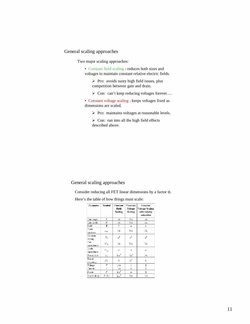
General scaling approaches
Two major scaling approaches:
• Constant field scaling- reduces both sizes and voltages to maintain constant relative electric fields. Pro: avoids nasty high field issues, plus
competition between gate and drain. Con: can’t keep reducing voltages forever….
• Constant voltage scaling- keeps voltages fixed as dimensions are scaled. Pro: maintains voltages at reasonable levels. Con: run into all the high field effects
described above.
General scaling approaches
Consider reducing all FET linear dimensions by a factor α.
Here’s the table of how things must scale:

12
Empirical scaling formulae
)14,21max( 55.077.0 lltox ××≈
75.05 lVDD ×≈
6.116104 −×≈ lNB
Assuming effective channel length l in microns, empirical data on “good” transistors predicts:
oxide thickness (nm)
supply voltage (V)
dopant density in bulk (cm-3)
From these empirical formula, can derive other quantities:
Dopant density must go up to avoid punch-through.
75.242 102.22/ lVCU xg ×=≡ minimal switching energy (can run into discreteness of levels….)
3.255.0 lVth ≈ threshold decrease due to DIBL….
Summary:
• A number of device physics issues crop up if one attempts to aggressively scale standard Si MOSFETs.
• Typical resulting problems:
• gate no longer effectively controls source-drain current
• substantial currents even when device should be “off”
• carrier behavior differs from that in larger devices
• There are ways of scaling that minimize these effects, but there’s no avoiding the eventual impending demise of scaling this device configuration.

13
Next time:
There are a number of competing candidate CMOS solutions to try and get around both the device engineering problems discussed today, and some of the fabrication and diagnostic issues mentioned last time.
Typical approaches:
• Change the gate geometry substantially to mitigate field problems.
• Change overall device shape to improve fabrication process and yield.
• Materials changes.
1
Alternatives to standard MOSFETs
A number of alternative FET schemes have been proposed, with an eye toward scaling up to the 10 nm node. Modifications to the standard MOSFET include:
• Silicon-in-insulator
• Silicon-on-”nothing”
• Double-gate FETs
• FinFETs
• Vertical FETs
• Vertical replacement gate FET
• Ballistic FET
• Tunneling FET
What problems are we really trying to solve?
There are several specific device physics problems that are addressed by these proposals:
• Short-channel effects (lack of saturation of ID)
• Short-channel threshold modification (drain-induced barrier lowering)
• Parasitics and isolation
• Doping problems and punchthrough
There are also manufacturing / engineering problems:
• Lithographic definition of very short channels
• Alignment of gate electrode with channel

2
Silicon-on-insulator
The basic idea:
ordinary MOSFET
“partially depleted” SOI
“fully depleted” SOI
Build transistors on a buried oxide layer rather than on bulk doped Si.
• Lowers source and drain capacitance to increase speeds.
• Reduces parasitic effects (e.g. unintentional bipolar transistor action).
• Solving Poisson’s equation shows reduced “body” effects such punch-through + VT
modifications.
Silicon-on-insulator
“partially depleted” SOI “fully depleted” SOI
• Partially depleted SOI: still some small “body” that can lead to slower speeds + parasitic effects.
• Fully depleted SOI: best possible situation, but considerablytougher to fabricate with high quality.
How to produce buried oxide layer?
• Oxygen implantation + annealing
• Growth (epitaxy) on top of preexisting insulator
• Wafer bonding

3
Silicon-on-insulator
• IBM already selling high-performance chips based on SOI technology.
• Much interest in SOI from MEMS community (sacrificial layers) + telecommunications (integration of optical waveguides, amplifiers) also.
image from IBM
Silicon-on-“nothing”
Basic idea: use an extremely thin dielectric (or even air!) cavity under the channel.
Gives the benefits of fully depleted SOI, but may not require whole-wafer SOI processing.
Takes advantage of selective etching of well-controlled sacrificial SiGe layer.

4
Double-gate FET
Best way to mitigate drain influence is to increase field effects of gate.
One method: double-gating.
Double-gate FET
Ideal DGFET shown at right.
Design minimizes parasitics and coupling capacitances.
For devices this small, quantum effects are significant:
Both symmetric DGFETs and backgate FETs have threshold voltages substantially greater (~100% !) than just classical electrostatic prediction.

5
Double-gate FET
Double-gate and FinFETs
The scheme on the previous page shows one approach: again using a sacrificial layer (with very well-controlled thickness) to define a critical dimension: the channel thickness.
Another version of this is the FinFET:
• Uses a thin “fin” of Si as the channel, and wraps the gate around/over the fin.
• Allows large (low resistance) source & drain contacts.

6
FinFET
Vertical FET
An alternative geometry.
Engineering:
• Channel length set by layer thickness rather than lithography.
• Packing density not set by channel length anymore.
• Wrap-around gate possible.
• Stronger confinement effects than planar devices.

7
Vertical FET
Gate = highly doped polysilicon.
To find VT, must keep track of bands throughout device.
Images from Oh thesis
Voffset
Criterion for inversion: when potential at channel/oxide interface is some small voltage Voffset below conduction band.
Bands in channel bend until depletion; then all shift.
source-drain
Vertical FET
Voffsetsource-drain
Rectangular double-gate MOSFET Threshold voltage: 02 εε x
xSiAoffsetoffsetoxT
tteNVVVV +−=−=
Cylindrical vertical MOSFET threshold voltage: ++−=−=
Si
xSi
x
SiAoffsetoffsetoxT r
trreNVVVV ln
2 0
2
εε
Here, tx = oxide thickness, εx = oxide dielectric constant.

8
Vertical replacement gate FET
One particular implementation of the vertical MOSFET.
Lucent team (Hergenrother, Monroe) developed to be fully compatible with standard CMOS processing for easy integration:
Vertical replacement gate FET

9
VRG FET
VRG FET

10
Ballistic FETs
For smallest devices, it’s possible to make FETs with channels smaller / shorter than the elastic mean free path in Si.
Room temperature mobility ~ 200 cm2/Vs
Direction-averaged effective mass in Si ~ 0.31 m0
Result: τ ~ 3.5 x 10⁻¹⁴ s.
Assuming a nondegenerate source of carriers at room temperature, vT = thermal velocity ~ (2kBT/m*)1/2 = 1.7x10⁵ m/s.
Typical elastic mean free path: ~ 6 nm.
Next lecture we’ll go into these devices in more detail; merges with Landauer-Buttiker picture….
Tunneling FET
• Special case of a quantum-limited FET.
• We already know tunneling probability depends exponentially on barrier height.
• We also know effective barrier can be controlled using a gate - essentially, carriers traversing the barrier region feel the (screened) gate potential.
• It’s possible to make a transistor where tunneling is the dominant transport mechanism.
Two examples:
• Double quantum well tunneling (Sandia)
• Metal-oxide-metal tunneling (ONR)

11
Tunneling FET
Downsides:
• Uses GaAs.
• Works at 77K.
• Requires thinned-down sample (back-side processing).
Upsides:
• Can be extremely fast (THz speeds).
• More functionality than just regular FET.
• No short-channel effects, effectively.
Metal tunneling FET
Start with metal strip (Ti, Al, Nb).
Use AFM to electrochemically oxidize a ~10-30 nm wide line across strip to act as tunnel barrier.
Substrate is gate in prototype.
Can get significant modulation of tunneling barrier.
Upsides: all metal (!), no short channel effects.
Downsides: labor intensive; fragile; not defect tolerant.
12
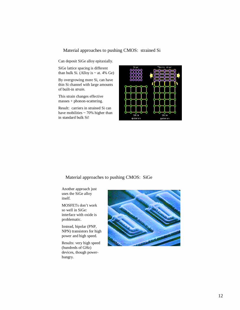
Material approaches to pushing CMOS: strained Si
Can deposit SiGe alloy epitaxially.
SiGe lattice spacing is different than bulk Si. (Alloy is ~ at. 4% Ge)
By overgrowing more Si, can have thin Si channel with large amounts of built-in strain.
This strain changes effective masses + phonon-scattering.
Result: carriers in strained Si can have mobilities ~ 70% higher than in standard bulk Si!
Material approaches to pushing CMOS: SiGe
Another approach just uses the SiGe alloy itself.
MOSFETs don’t work so well in SiGe: interface with oxide is problematic.
Instead, bipolar (PNP, NPN) transistors for high power and high speed.
Results: very high speed (hundreds of GHz) devices, though power-hungry.
13
Summary:
• A number of clever device-design approaches to mitigating the problems that can crop up in small CMOS devices.
• Recurring theme: using layer thicknesses rather than lithography to define critical length scales.
• Recurring theme: quantum effects can become important (or even essential) in device properties at ~ 10 nm scale.
• Material engineering can be promising as well.
Next time:
The ballistic transistor: where Landauer-Buttiker meets higher temperatures and practical (?) devices.
After that:
Coulomb blockade and single-electron transistors
Molecular electronics
Organic electronics
1
Ballistic nanotransistors
Modeled on analysis by Mark Lundstrom (ECE, Purdue). Unless otherwise indicated, all images are his.
Interesting hybrid of classical transistor behavior, quantum confinement effects, and Landauer-Buttiker type ideas.
Device parameters:
Length: L > ~ 10 nm to avoid contributions of direct source-drain tunneling.
First look at effects of confinement and see what we can neglect.
Subbands and quantum confinement
This problem is essentially something we’ve done several times before.
One can solve the Schroedinger equation for neutral, noninteracting particles confined in two dimensions but extended in the third.
This is effectively a 1d quantum system, with 1d subbands separated in energy by spacings that look like those between low-lying levels of a 2d particle in a box.
As usual, we recall that one can consider the envelope function of Bloch waves, and arrive at an identical equation for the single-particle levels for non-interacting electrons.
2
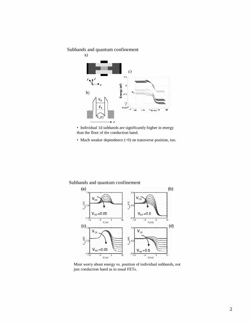
Subbands and quantum confinement
• Individual 1d subbands are significantly higher in energy than the floor of the conduction band.
• Much weaker dependence (~0) on transverse position, too.
Subbands and quantum confinement
Must worry about energy vs. position of individual subbands, not just conduction band as in usual FETs.

3
Complete solution
In generality, one must self-consistently solve the electrostatic and quantum mechanical problems.
Generally this is requires numerical solution, but it is possible to come up with analytical expressions in certain limits.
First, we’ll look qualitatively at what happens as gate and drain bias are varied.
Then we’ll consider three regimes:
T >> 0 -- nondegenerate carriers
T ~ 0 -- degenerate carriers
T > 0 -- general case.
Nonequilibrium velocity (momentum) distributions
Remember our Landauer formula discussions? We worked in 1d and considered the chemical potential at different places along a device:
Tcontact 1 contact 2
lead 1 lead 2
µ1 µ1 µ1µ1µ2µ1 µ2µ1 µ2µ1 µ2µ1µ2 µ2µ2µ2
1
Can do same thing here, but plot velocity (momentum) distributions as a function of position:

4
Nonequilibrium velocity (momentum) distributions
In source at top of barrier
near drain in drain
Plots for case of high gate voltage and high drain voltage, finite temperature.
Nonequilibrium velocity (momentum) distributions
Now fix gate bias.
Examine distributions as function of drain bias at top of barrier.
At low VD, carriers pass over the barrier in both directions.
As VD is increased, higher fraction of carriers getting over barrier are from the source.
At sufficiently large VD, no carriers from drain reach top of barrier.
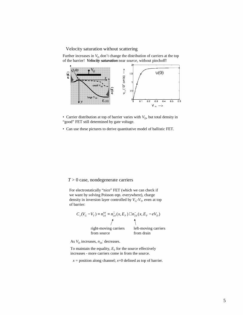
Further increases in VD don’t change the distribution of carriers at the top of the barrier! Velocity saturation near source, without pinchoff!
5
Velocity saturation without scattering
Further increases in VD don’t change the distribution of carriers at the top of the barrier! Velocity saturation near source, without pinchoff!
• Carrier distribution at top of barrier varies with VD, but total density in “good” FET still determined by gate voltage.
• Can use these pictures to derive quantitative model of ballistic FET.
T > 0 case, nondegenerate carriers
For electrostatically “nice” FET (which we can check if we want by solving Poisson eqn. everywhere), charge density in inversion layer controlled by VG-VT, even at top of barrier:
),(),()( 222 DFdFdtotdTGx eVExnExnnVVC −+==− −+
right-moving carriers from source
left-moving carriers from drain
As VD increases, n2d- decreases.
To maintain the equality, EF for the source effectively increases - more carriers come in from the source.
x = position along channel; x=0 defined as top of barrier.

6
T > 0 case, nondegenerate carriers
Net current is, similarly, given by an expression familiar from our Landauer picture:
)()( DFFD eVEIEII −−= −+
Velocity distribution of right moving carriers is hemi-Maxwellian: ∑
>
=⋅=yx pp
BMxT m
TkEfvv
,0 *
2)(
π
Maxwell-Boltzmann distribution.
Same argument works for left-moving carriers, so their average speed is essentially identical to that of the right-movers.
T > 0 case, nondegenerate carriers
Resulting current density:
TdTdD venvenWI )0()0(/ 22++ −=
))0(/)0(1(
))0(/)0(1(/
22
222 −+
−+
+−=
dd
ddT
totdD nn
nnvenWI
Ahh, but we can figure out the ratio n2d+/n2d
- : −=+
Tk
EENn
B
Fdd exp
22
2 −−=−
Tk
EeVENn
B
DFdd exp
22
2
where Tkm
N Bd = 2*
2 hπ
Effective density of states

7
T > 0 case, nondegenerate carriers
Result for current density:
)1(
)1(/ /
/
2 TkeV
TkeV
TtotdD BD
BD
e
evenWI −
−
+−=
))0(/)0(1(
))0(/)0(1(/
22
222 −+
−+
+−=
dd
ddT
totdD nn
nnvenWI
Plugging in our expression for carrier density in a “nice” FET gives:
)1(
)1()( /
/
TkeV
TkeV
TTGxD BD
BD
e
evVVWCI −
−
+−−=
ID
VD
T > 0 case, nondegenerate carriers - saturation
ID
VD
There is saturation at high VD, because all current is determined by charge density at top of barrier, where effective velocity saturates out to the hemi-Maxwell mean velocity.
Unlike the standard MOSFET, VDsat is independent of VG:
)1(
)1()( /
/
TkeV
TkeV
TTGxD BD
BD
e
evVVWCI −
−
+−−=
e
TkV B
Dsat
2≈
For VD >> Vdsat,
TTGxDsat vVVWCI )( −=

8
T > 0 case, nondegenerate carriers – linear regime
)1(
)1()( /
/
TkeV
TkeV
TTGxD BD
BD
e
evVVWCI −
−
+−−=
ID
VD
We can expand
for small eVD/kBT to find linear regime behavior:
DB
TTGxD V
eTk
vVVWCI −≈
/2)(
So, channel conductanceeTk
I
eTk
vVVWCG
B
Dsat
B
TTGx /2/2)( =−=
Regular MOSFET hasL
VVWCG TGx
µ)( −=
Since regular MOSFET can never be better than ballistic case,
TB ve
Tk
L<→ 2µ Upper limit on mobility….
T > 0 case, nondegenerate carriers – linear regime
Note that channel conductance is finite even for ballistic case, as in Landauer picture.
Here, it’s a direct consequence of the thermionic emission model used here when examined at small bias.
Left-moving current down from right-moving current by exp(-eVD/kBT)
eTk
vVVWCG
B
TTGx /2)( −=

9
T ~ 0, degenerate case, linear regime
Still have
DF
DFF eVE
IeVEIEI ∂
∂≈−−+
−+ )()(
)()( DFFD eVEIEII −−= −+
22*
2/3*
*2
3
3
)2(
3)( hh
ππ m
EmeW
m
keWEI FF
F ==+
Assuming hard transverse walls, transverse modes spaced by (π/W) in k space,
Result: DF
D VWk
h
eI =
π
22
This is the Landauer expression, with M, the number of channels, given by
W
kM F
/π= DD V
h
eMI =
22
T ~ 0, degenerate case, “saturated” regime
If transistor is “on” all the way, current is just I+ :
*2
3
3)(
m
keWEI F
F πh=+
For 2d gas (one vert. subband, many transverse modes), all the right-moving carriers must be due to gate:
e
VVCkn TGxFtot
d
)(
4
2
2
−==π
Plugging in, −−= πqVVCm
VVWCI TGxTGxDsat /)(3
8)(
*
h

10
T ~ 0, degenerate case, “saturated” regime
Generically, for ballistic FET, Idsatvaries like (VG-VT)α.
For nondegenerate case, α = 1.
For degenerate case, α = 3/2.
Saturation happens when VD pulls right contact Fermi level below bottom of conduction band.
This happens here:
)()2/( 2
2 TGd
xDsat VV
e
CV −=
ν
General finite temperature results:
Defining the general Fermi-Dirac integral of order s as:∫∞
−−≡
0 1)exp()(
ηη
x
dxxF
s
s
and the normalized drain voltage: )//( eTkVU BDD ≡
we find: −+−−−=
)(/)(1
)(/)(1~)(00
2/12/1
FDF
FDFTTGxD FUF
FUFvVVeWCI
ηηηη
and the normalized Fermi energy: TkE BFF /)( 1εη −≡
where:
)(
)(2~
0
2/1
* F
FBT F
F
m
Tkv
ηη
π=
11
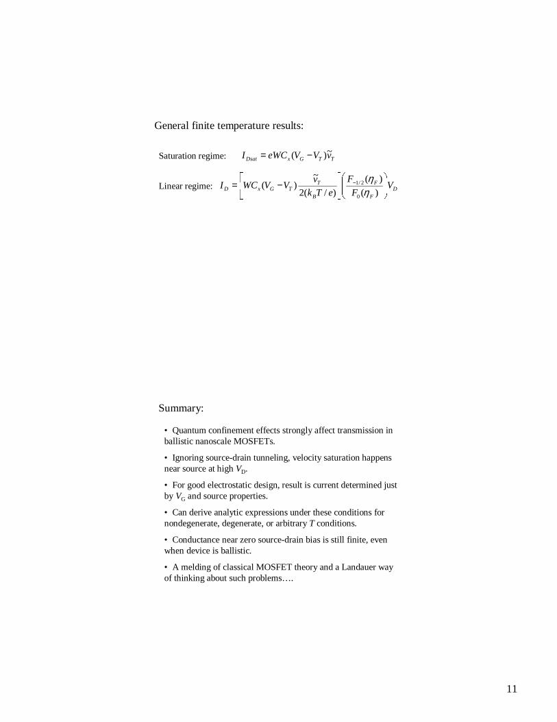
General finite temperature results:
Saturation regime: TTGxDsat vVVeWCI ~)( −=
Linear regime: DF
F
B
TTGxD V
F
F
eTk
vVVWCI −= −
)(
)(
)/(2
~)(
0
2/1
ηη
Summary:
• Quantum confinement effects strongly affect transmission in ballistic nanoscale MOSFETs.
• Ignoring source-drain tunneling, velocity saturation happens near source at high VD.
• For good electrostatic design, result is current determined just by VG and source properties.
• Can derive analytic expressions under these conditions for nondegenerate, degenerate, or arbitrary T conditions.
• Conductance near zero source-drain bias is still finite, even when device is ballistic.
• A melding of classical MOSFET theory and a Landauer way of thinking about such problems….

12
Next time:
• Coulomb Blockade physics
• Single-electron devices as successors to MOSFETs?