motion controller for stepper motors integrated circuits · pdf filemotion controller for...
TRANSCRIPT
MOTION CONTROLLER FOR STEPPER MOTORS INTEGRATED CIRCUITS
TRINAMIC Motion Control GmbH & Co. KG Hamburg, Germany
TMC429 DATASHEET
Intelligent Triple Stepper Motor Controller with Serial Peripheral Interfaces and Step/Direction Full Compatible Successor of the TMC428
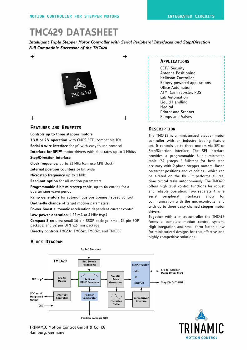
BLOCK DIAGRAM
FEATURES AND BENEFITS Controls up to three stepper motors
3.3 V or 5 V operation with CMOS / TTL compatible IOs
Serial 4-wire interface for µC with easy-to-use protocol
Interface for SPI™ motor drivers with data rates up to 1 Mbit/s
Step/Direction interface
Clock frequency: up to 32 MHz (can use CPU clock)
Internal position counters 24 bit wide
Microstep frequency up to 1 MHz
Read-out option for all motion parameters
Programmable 6 bit microstep table, up to 64 entries for a quarter sine wave period
Ramp generators for autonomous positioning / speed control
On-the-fly change of target motion parameters
Power boost automatic acceleration dependent current control
Low power operation: 1.25 mA at 4 MHz (typ.)
Compact Size: ultra small 16 pin SSOP package, small 24 pin SOP package, and 32 pin QFN 5x5 mm package
Directly controls TMC23x, TMC24x, TMC26x, and TMC389
APPLICATIONS CCTV, Security Antenna Positioning Heliostat Controller Battery powered applications Office Automation ATM, Cash recycler, POS Lab Automation Liquid Handling Medical Printer and Scanner Pumps and Valves
DESCRIPTION The TMC429 is a miniaturized stepper motor controller with an industry leading feature set. It controls up to three motors via SPI or Step/Direction interface. The SPI interface provides a programmable 6 bit microstep table (64 µsteps / fullstep) for best step accuracy with 2-phase stepper motors. Based on target positions and velocities - which can be altered on the fly - it performs all real time critical tasks autonomously. The TMC429 offers high level control functions for robust and reliable operation. Two separate 4 wire serial peripheral interfaces allow for communication with the microcontroller and with up to three daisy chained stepper motor drivers. Together with a microcontroller the TMC429 forms a complete motion control system. High integration and small form factor allow for miniaturized designs for cost-effective and highly competitive solutions.
TMC429
SPI to Master
CLK
Position Comparator
InterruptController
Ref. Switch Processing
Step/DirPulse
Generation
OUTPUT SELECT
- SPI
or
- Step/Dir
Microstep Table
Serial Driver Interface
3x Ref. Switches
3x Linear RAMP Generator
SPI to Stepper Motor Driver 0/1/2
Step/Dir OUT 0/1/2SPI to µC
SDO to µC Muliplexed Output
Position Compare OUT
TMC429 DATASHEET (Rev. 2.04 / 2015-JUN-03) 2
www.trinamic.com
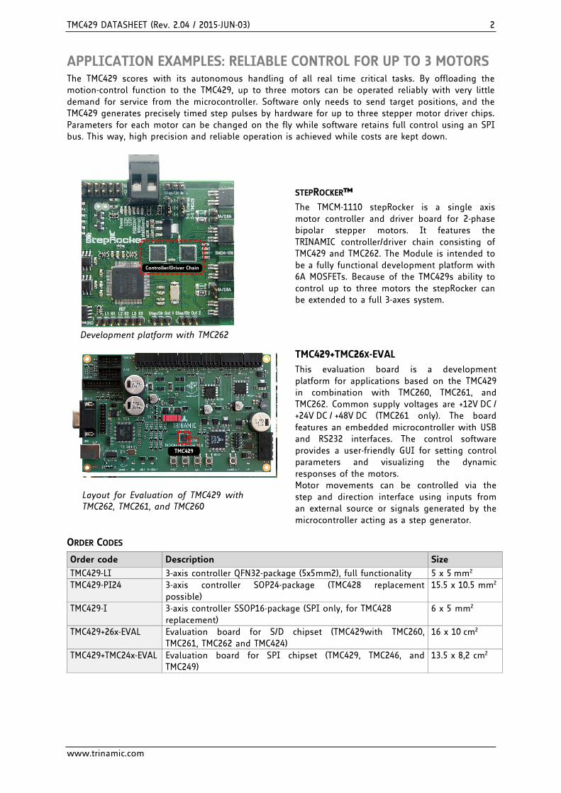
Layout for Evaluation of TMC429 with TMC262, TMC261, and TMC260
APPLICATION EXAMPLES: RELIABLE CONTROL FOR UP TO 3 MOTORS The TMC429 scores with its autonomous handling of all real time critical tasks. By offloading the motion-control function to the TMC429, up to three motors can be operated reliably with very little demand for service from the microcontroller. Software only needs to send target positions, and the TMC429 generates precisely timed step pulses by hardware for up to three stepper motor driver chips. Parameters for each motor can be changed on the fly while software retains full control using an SPI bus. This way, high precision and reliable operation is achieved while costs are kept down.
Controller/Driver Chain
Development platform with TMC262
TMC429
ORDER CODES
Order code Description Size
TMC429-LI 3-axis controller QFN32-package (5x5mm2), full functionality 5 x 5 mm2 TMC429-PI24 3-axis controller SOP24-package (TMC428 replacement
possible) 15.5 x 10.5 mm2
TMC429-I 3-axis controller SSOP16-package (SPI only, for TMC428 replacement)
6 x 5 mm2
TMC429+26x-EVAL Evaluation board for S/D chipset (TMC429with TMC260, TMC261, TMC262 and TMC424)
16 x 10 cm2
TMC429+TMC24x-EVAL Evaluation board for SPI chipset (TMC429, TMC246, and TMC249)
13.5 x 8,2 cm2
STEPROCKER™ The TMCM-1110 stepRocker is a single axis motor controller and driver board for 2-phase bipolar stepper motors. It features the TRINAMIC controller/driver chain consisting of TMC429 and TMC262. The Module is intended to be a fully functional development platform with 6A MOSFETs. Because of the TMC429s ability to control up to three motors the stepRocker can be extended to a full 3-axes system.
TMC429+TMC26X-EVAL This evaluation board is a development platform for applications based on the TMC429 in combination with TMC260, TMC261, and TMC262. Common supply voltages are +12V DC / +24V DC / +48V DC (TMC261 only). The board features an embedded microcontroller with USB and RS232 interfaces. The control software provides a user-friendly GUI for setting control parameters and visualizing the dynamic responses of the motors. Motor movements can be controlled via the step and direction interface using inputs from an external source or signals generated by the microcontroller acting as a step generator.

TMC429 DATASHEET (Rev. 2.04 / 2015-JUN-03) 3
www.trinamic.com
TABLE OF CONTENTS 1 PRINCIPLES OF OPERATION 4
1.1 KEY CONCEPTS 4 1.2 CONTROL INTERFACES 5 1.3 SOFTWARE VISIBILITY 6 1.4 STEP FREQUENCIES 6 1.5 MOVING THE MOTOR 7
2 GENERAL DEFINITIONS, UNITS, AND NOTATIONS 9
2.1 NOTATIONS 9 2.2 SIGNAL POLARITIES 9 2.3 UNITS OF MOTION PARAMETERS 9 2.4 REPRESENTATION OF SIGNED VALUES BY TWO’S
COMPLEMENT 9
3 PACKAGE VARIANTS 10
4 PIN ASSIGNMENTS 10
4.1 PACKAGE OUTLINES 11 4.2 SIGNAL DESCRIPTIONS 12
5 SAMPLE CIRCUITS 13
5.1 APPLICATION EXAMPLE: TMC429 IN QFN32
PACKAGE 13 5.2 APPLICATION EXAMPLE: TMC429 IN SSOP16
PACKAGE 14 5.3 APPLICATION EXAMPLE: TMC429 WITH DRIVERS
WITHOUT SERIAL DATA OUTPUT (SDO) 14
6 CONTROL INTERFACE 15
6.1 BUS SIGNALS 15 6.2 SERIAL PERIPHERAL INTERFACE FOR µC 15
7 ADDRESS SPACE PARTITIONS 20
7.1 READ AND WRITE 20 7.2 REGISTER SET 20 7.3 REGISTER MAPPING 21
8 REGISTER DESCRIPTION 22
8.1 AXIS PARAMETER REGISTERS 22 8.2 GLOBAL PARAMETER REGISTERS 39
9 REFERENCE SWITCH INPUTS 49
9.1 REFERENCE SWITCH CONFIGURATION, MOT1R, AND REFMUX 49
9.2 TRIPLE SWITCH CONFIGURATION 51 9.3 HOMING PROCEDURE 52 9.4 SIMULTANEOUS START OF UP TO THREE STEPPER
MOTORS 52
10 STEP/DIR DRIVERS 53
10.1 TIMING 53
11 SPI MODE DRIVER INTERFACE 54
11.1 BUS SIGNALS 54 11.2 TIMING 54 11.3 RAM ADDRESS PARTITIONING AND DATA
ORGANIZATION 55 11.4 STEPPER DRIVER SPI DATAGRAM CONFIGURATION
57 11.5 INITIALIZATION OF MICROSTEP LOOK-UP TABLE62
12 RUNNING A MOTOR 67
12.1 GETTING STARTED 67 12.2 RUNNING A MOTOR WITH START-STOP-SPEED IN
RAMP_MODE 67
13 ON-CHIP VOLTAGE REGULATOR 68
14 POWER-ON RESET 69
15 ABSOLUTE MAXIMUM RATINGS 70
16 ELECTRICAL CHARACTERISTICS 70
16.1 POWER DISSIPATION 70 16.2 DC CHARACTERISTICS 71 16.3 TIMING CHARACTERISTICS 72
18 PACKAGE MACHANICAL DATA 73
18.1 TMC429-LI / QFN32 73 18.2 TMC429-PI24 / SOP24 74 18.4 TMC429-I / SSOP16 75
19 MARKING 76
20 COMPATIBILITY INFORMATION: TMC429 AND TMC428 77
20.1 SIGNAL DESCRIPTIONS: TMC428 VS. TMC42977 20.2 TMC428 SDO_C OUTPUT 78 20.3 UNUSED ADDRESSES 78 20.4 GENERAL TIMING PARAMETERS 79
21 DISCLAIMER 80
22 ESD SENSITIVE DEVICE 80
23 TABLE OF FIGURES 81
24 REVISION HISTORY 82
25 REFERENCES 83

TMC429 DATASHEET (Rev. 2.04 / 2015-JUN-03) 4
www.trinamic.com
1 Principles of Operation
Serial µC
Interface
3 x RAMP Generator
3 x STEPPULS Generator
3x Step/Dir
MicrostepUnit
(incl. Sequencer)
Serial DriverInterface
Multiple Ported RAM
MUX
SPI Mode
6
VoltageRegulator
GND
Power-on Reset
POSCOMP
Interrupt Controller
REF
1REF
2REF
3
REF
1R*
REF
2R*
REF
3R*
nSCS_C
SCK_C
SDI_C
nINT_SDO_C
TEST
SDOZ_C*nSCS_S / Step 2SCK_S / Dir 1SDO_S / Step 1
SDI_S / Dir 2
nSCS3 / Dir 3*nSCS2 / Step 3*
470nF
POSCMP*
CLK4-32MHz
GND
DIE PAD
GND GND
100nF
TMC429
GND
V5 /+5V supply or +3V supply
* Not available with all IC packages. Please refer to the package outlines.
SPI
SPI / Step/Dir
to driver
SPI to
µC
Connect for +3.3V operation
V33
V5
Figure 1.1 TMC429 functional block diagram
The TMC429 is a miniaturized high performance stepper motor controller with an outstanding cost-performance ratio. It is designed for high volume automotive as well as for demanding industrial motion control applications. Once initialized the TMC429 controls up to three 2-phase stepper motors simultaneously. A programmable sequencer for 2-phase motors is integrated. The TMC429 motion controller is equipped with an SPI™ host interface with easy-to-use protocol and two driver interfaces (SPI and STEP/DIR) for addressing various stepper motor driver types.
1.1 Key Concepts The TMC429 realizes real time critical tasks autonomously and guarantees for a robust and reliable drive. These following features contribute toward greater precision, greater efficiency, higher reliability, and smoother motion in many stepper motor applications. Initialization Adapt the TMC429 to the driver type and configuration and send initial configuration
data to SPI drivers. Configure microstep resolution and waveform for SPI drivers. Interfacing The TMC429 offers application specific interfacing via Step/Dir or SPI. Positioning The TMC429 operates the motors based on user specified target positions and
velocities. Modify all motion target parameters on-the-fly during motion. Programming Every parameter can be changed at any time. The uniform access to any TMC429
register simplifies application programming. A read-back option for all internal registers is available.
Microstepping Based on internal position counters the TMC429 performs up to ±223 (micro)steps completely independent from the microcontroller. Microstep resolutions are individually programmable for each stepper motor.
The range goes from full stepping (1 microstep = 1 full step) and half stepping (2 microsteps per full step) up to 6 bit micro stepping (64 microsteps per full step) for precise positioning and noiseless stepper motor rotation. With STEP/DIR drivers any microstep resolution is possible as supported by the driver. The internal microstep table can be adapted to specific motor characteristics to further reduce torque ripple, if desired.

TMC429 DATASHEET (Rev. 2.04 / 2015-JUN-03) 5
www.trinamic.com
1.2 Control Interfaces
1.2.1 Serial µC Interface From the software point of view, the TMC429 provides a set of registers, accessed by a microcontroller via a serial interface in a uniform way. Each datagram contains address bits, a read-write selection bit, and data bits to access the registers and the on-chip memory. Each time the microcontroller sends a datagram to the TMC429 it simultaneously receives a datagram from the TMC429. This simplifies the communication with the TMC429 and makes programming easy. Most microcontrollers have an SPI hardware interface, which directly connects to the serial four wire microcontroller interface of the TMC429. For microcontrollers without SPI hardware software doing the serial communication is sufficient and can easily be implemented.
1.2.2 Step/Dir Driver Interface The TMC429-LI controls the motor position by sending pulses on the STEP signal while indicating the direction on the DIR signal. A programmable step pulse length and step frequencies up to 1MHz allow operation at high speed and high microstep resolution. The driver chip converts these signals into the coil currents which control the position of the motor. The TMC429-LI perfectly fits to the TMC26x smart power Step/Dir driver family.
µCHigh Level Interface
Stepper Motor Driver
e.g. TMC260/TMC261
M
Motor 3
Stepper Motor Driver
e.g. TMC260/TMC261
M
Motor 2
Stepper Motor Driver
e.g. TMC260/TMC261
M
Motor 1
TMC429Motion Controller
SPI
Step/Dir 1 Step/Dir 3Step/Dir 2SPI
Figure 1.2 Application example using Step/Dir driver interface
1.2.3 Serial Driver Interface The TMC429 automatically generates the required data-stream for SPI drivers and provides user configurable microstep waves and motor ramps for up to three motors. The serial interface to the motor drivers is flexibly configurable for different types (from different vendors) with up to 64 bit length for the SPI daisy chain. The TMC429-I perfectly fits to the TMC24x driver family.
µCHigh Level Interface
Stepper Motor Driver
e.g. TMC236/TMC246
M
Motor 3
Stepper Motor Driver
e.g. TMC236/TMC246
M
Motor 2
Stepper Motor Driver
e.g. TMC236/TMC246
M
Motor 1
TMC429Motion Controller
SPI
SPI
Figure 1.3 Application example using SPI driver interface

TMC429 DATASHEET (Rev. 2.04 / 2015-JUN-03) 6
www.trinamic.com
1.3 Software Visibility From the software point of view the TMC429 provides a set of registers and on-chip RAM (see Figure 1.1), accessed via the serial µC interface in a uniform way. The serial interface uses a simple protocol with fixed datagram length for the read- and write-access. These registers are used for initializing the chip as required by the hardware configuration. Afterwards the motor can be moved by writing target positions or velocity and acceleration values.
1.4 Step Frequencies The desired motor velocity is an important design parameter of an application. Therefore it is important to understand the limiting factors.
1.4.1 Step Frequencies using the Step/Dir driver interface The step pulses can directly be fed to a Step/Dir driver. The maximum full step rate (fsfmax) depends on the microstep resolution of the external driver chip.
The TMC429 microstep rate (µsf) is up to 1/32 of the clock frequency:
µ𝑠𝑠f𝑚𝑚𝑚𝑚𝑚𝑚 =fCLK32
EXAMPLE FOR FULL STEP FREQUENCY CALCULATION fCLK = 16 MHz µsfmax = 500 kHz µstep resolution of external driver: 16
𝑓𝑓𝑠𝑠𝑓𝑓𝑚𝑚𝑚𝑚𝑚𝑚 = 500 𝑘𝑘𝑘𝑘𝑘𝑘
16= 31.25 𝑘𝑘𝑘𝑘𝑘𝑘
With a standard motor with 1.8° per full step this results in up to 31.25kHz/200= 156 rotations per second, which is far above realistic motor velocities for this kind of motor and thus imposes no real limit on the application.
A 16 microsteps resolution can be extrapolated to 256 microsteps within the driver when using the TMC26x driver family.
1.4.2 Step frequencies using the SPI driver interface The microstep unit with included sequencer processes step pulses from the pulse generator, which represent microsteps, half steps, or full steps (depending on the selected step resolution). The serial driver interface sends datagrams to the stepper motor driver chain whenever a step pulse comes. The theoretical microstep frequency is identical to Step/Dir mode, but the achievable step frequency may be limited by the SPI data rate. Maximum SPI frequency (bit rate) is clock frequency divided by 16 (when CLK2DIV=7). An overhead of 1.5 bits is required per datagram. The maximum microstep transmission frequency depends on the total length of the datagrams sent to the SPI stepper motor driver chain.
EXAMPLE FOR SPI DATA RATE CALCULATION At a clock frequency of 16 MHz, with a daisy chain of three SPI stepper motor drivers of 12 bit datagram length each (e.g. TMC246), the theoretical maximum SPI transmission frequency (fSPImax) is:
𝑓𝑓𝑓𝑓𝑓𝑓𝑓𝑓𝑚𝑚𝑚𝑚𝑚𝑚 = 16 𝑀𝑀𝑘𝑘𝑘𝑘
163 × 12 + 1.5
This is approximately 27 kHz. It is the theoretical upper limit for the fullstep frequency. In an application, the maximum desired fullstep frequency should be a factor 4 to 8 lower in order to avoid a beat between the step frequency and the SPI transmission rate. The microstep rate may be higher than the SPI transmission frequency, even if the stepper motor driver does not note all microsteps due to the SPI data rate limit. At high step rates (respectively pulse rates) the differences between microstepping and full step excitation vanish.

TMC429 DATASHEET (Rev. 2.04 / 2015-JUN-03) 7
www.trinamic.com
1.5 Moving the Motor Moving the motor is simple: - To move a motor to a new target position, write the target position into the associated register
by sending a datagram to the TMC429. - To move a motor with a new target velocity, write the velocity into the register assigned to the
stepper motor.
1.5.1 Motion Controller Functionality The ramp generator monitors the motion parameters stored in its registers and calculates velocity profiles. Based on the actual ramp generator velocity a pulse generator supplies step pulses to the motor driver.
1.5.2 Modes of Motion – Individually Programmable for Each Axis ramp_mode For positioning applications the ramp_mode is most suitable. The user sets the
position and the TMC429 calculates a trapezoidal velocity profile and drives autonomously to the target position. During motion, the position may be altered arbitrarily.
velocity_mode For constant velocity applications the velocity_mode is most suitable. In velocity_mode, a target velocity is set by the user and the TMC429 takes into account user defined limits of velocity and acceleration.
hold_mode In hold_mode, the user sets target velocities, but the TMC429 ignores any limits of velocity and acceleration, to realize arbitrary velocity profiles, controlled completely by the user.
soft_mode The soft_mode is similar to the ramp_mode, but the decrease of the velocity during deceleration is done with a soft, exponentially shaped velocity profile.
1.5.3 Interrupts The TMC429 has capabilities to generate interrupts. Interrupts are based on ramp generator conditions which can be set using an interrupt mask. The interrupt controller (which continuously monitors reference switches and ramp generator conditions) generates an interrupt if required.
SPECIAL HANDLING: TMC429-I / 16-PIN PACKAGE - On 16-pin package the SDO_C signal becomes a low active interrupt signal called nINT_SDO_C
while nSCS_C is high. Set SDO_INT=1 to access the non-multiplexed interrupt signal output nINT_SDO_C for the other packages.
- If the microcontroller disables the interrupt during access to the TMC429 and enables the interrupt otherwise, the multiplexed interrupt output of the TMC429 behaves like a dedicated interrupt output.
- For polling, the TMC429 sends the status of the interrupt signal to the microcontroller with each datagram.
1.5.4 Reference Switch Handling The TMC429 has a left and a right reference switch input for each motor. Note, that these inputs are not available with all packages.
SPECIAL HANDLING: TMC429-I / 16-PIN PACKAGE Because of its 16-pin package the TMC429-I has only three reference switch inputs: REF1, REF2, and REF3. Therefore the TMC429-I provides two different modes for reference switch handling:
- In the Default Reference Switch Mode the three reference switch inputs are defined as left side reference switches, one for each stepper motor.
- The Second Reference Switch Mode defines the first reference input REF1 as left reference switch input of motor one, the second reference input REF2 as left reference switch input of motor two, and the 3rd reference input REF3 as right reference switch input of motor one. In the second reference switch mode there is no reference switch input available for stepper motor three.
- With an external multiplexer 74HC157 any stepper motor may have a left and a right reference switch.

TMC429 DATASHEET (Rev. 2.04 / 2015-JUN-03) 8
www.trinamic.com
1.5.5 Integrated Programmable µstep Sequencer The serial SPI interface to the stepper motor driver chain has to be configured by an initialization sequence which writes the configuration into the on-chip RAM. Once configured the serial driver interface works autonomously. The internal multiple port RAM controller of the TMC429 takes care of access scheduling. So, the user may read and write registers and on-chip RAM at any time. The registers hold global configuration parameters and motion parameters. The on-chip RAM stores the configuration of the serial driver interface and the microstep table. The sequencer internally generates a number of control signals available for transmission to SPI driver ICs. These sequencer output signals are selected as configured by the internal stepper motor driver datagram configuration table. During power-on reset, the TMC429 initializes a default configuration within the on-chip RAM for an SPI driver chain for TMC23x and TMC24x stepper motor drivers.
1.5.6 Access to Status and Error Bits
STEP/DIR The microcontroller directly controls and monitors the stepper drivers. It also needs to take care for advanced current control, e.g. power down in stand still.
SPI Many serial stepper motor drivers provide status bits (driver active, inactive…) and error bits (short to ground, wire open…), which are sent back from the stepper motor driver chain to the motion controller. To have access to error bits and datagrams with a total length up to 48 bits the TMC429 buffers the information by means of two 24 bit wide registers. The microcontroller has direct access to these registers. Although, the TMC429 provides datagrams with up to 64 bits to the driver chain, only the last 48 bits sent back from the driver chain are buffered for read out by the microcontroller. Buffering of up to 48 bits is sufficient for a chain of three stepper motor drivers. For a chain of three TMC23x / TMC24x stepper motor driver chips all status bits are accessible.
TMC429 DATASHEET (Rev. 2.04 / 2015-JUN-03) 9
www.trinamic.com
2 General Definitions, Units, and Notations
2.1 Notations - Decimal numbers are used as usual without additional identification. - Binary numbers are identified by a prefixed % character. - Hexadecimal numbers are identified by a prefixed $ character.
EXAMPLE Decimal: 42 Binary: %101010 Hexadecimal: $2A
TMC429 DATAGRAMS ARE WRITTEN AS 32 BIT NUMBERS, E.G.: $1234ABCD = %0001 0010 0011 0100 1010 1011 1100 1101
TWO TO THE POWER OF N In addition to the basic arithmetic operators (+, -, *, /) the operator two to the power of n is required at different sections of this data sheet. For better readability instead of 2n the notation 2^n is used.
2.2 Signal Polarities External and internal signals are high active per default, but the polarity of some signals is programmable to be inverted. A pre-fixed lower case n indicates low active signals (e.g. nSCS_C, nSCS_S). See chapter 8.2, too.
2.3 Units of Motion Parameters The motion parameters position, velocity, and acceleration are given as integer values within TMC429 specific units. With a given stepper motor resolution one can calculate physical units for angle, angular velocity, angular acceleration. (See chapter 8.1.13)
2.4 Representation of Signed Values by Two’s Complement Motion parameters which have to cover negative and positive motion direction are processed as signed numbers represented by two’s complement as usual. Limit motion parameters are represented as unsigned binary numbers.
SIGNED MOTION PARAMETERS ARE: V_TARGET / V_ACTUAL / A_ACTUAL / A_THRESHOLD
UNSIGNED MOTION PARAMETERS ARE: V_MIN / V_MAX / A_MAX
POSITIONS X_TARGET / X_ACTUAL can be treated as signed or unsigned, as desired.

TMC429 DATASHEET (Rev. 2.04 / 2015-JUN-03) 10
www.trinamic.com
3 Package Variants The TMC429 is available in three different package variants, qualified for the industrial temperature range. An additional variant is available for the automotive temperature range. All package variants are RoHS compilant.
Order code Package Characteristics JEDEC Drawing
TMC429-LI QFN32 5x5mm, 32 pins, plastic package, industrial (-40… +85°C) MO-220 ?
TMC429-PI24 SOP24 300 mils, 24 pins, plastic package, industrial (-40… +85°C) MS-013 (300 mils)
TMC429-I SSOP16 150 mils, 16 pins, plastic package, industrial (-40… +85°C) MO-137 (150 mils)
4 Pin Assignments The three package variants of the TMC429 offer different signal sets for various applications:
Type Package Compatibility Remarks
TMC429-LI QFN32 - Full functionality including SPI and Step/Dir driver interfaces for up to three stepper motor driver chips
- Fits best to TMC26x and TMC389. TMC429-PI24 SOP24 TMC428-PI24
replacement
- SPI interface for up to three stepper driver chips - STEP/DIR interface for up to three stepper driver
chips - The right reference switch for motor 3 is not
available. TMC429-I SSOP16 TMC428-I
replacement - SPI interface for up to three stepper motor driver
chips (complements the TMC24x). - Step/Dir interface for up to two motors. - The additional reference right side switch inputs
REF1R, REF2R, and REF3R are not available. - An additional multiplexer 74hc157 might be
necessary. The multiplexing control signal is only available in SPI stepper motor driver chain mode.
Some third party SPI stepper motor drivers have no serial data output and therefore cannot simply be arranged in a daisy chain to drive more than one motor. The package variants SOP24 and QFN32 have two additional driver selection outputs nSCS2 and nSCS3 for stepper motor drivers without serial data output. All inputs are Schmitt-Trigger. Unused inputs (REF1, REF2, REF3, and SDI_S) need to be connected to ground. Unused reference switch inputs have to be connected to ground, too. A pull-down resistor is necessary at the SDI_S input of the TMC429 for those serial peripheral interface stepper motor drivers that set their serial data output to high impedance Z while inactive. STEP function outputs are S1, S2, and S3. Corresponding DIR outputs are D1, D2, and D3. The multiplexed output nINT_SDO_C of TMC429-LI and TMC429-PI24 can be configured in a de-multiplexed mode. An additional output named POSCMP is available for triggering when moving over a programmable position. Attention - After power on-reset, the TMC429 starts in TMC428 mode. That is, because the TMC429 is a 100%
compatible successor of the TMC428 motion controller. Additional outputs of the TMC429 including specific functions have to be activated by dedicated TMC429 configuration registers.
- Preferably, long wires to the reference switch inputs (REF1, REF2, and REF3) should be avoided. For long wires, a low pass filter for spike suppression should be provided (refer the TMC429 evaluation board schematic as example).
TMC429 DATASHEET (Rev. 2.04 / 2015-JUN-03) 11
www.trinamic.com
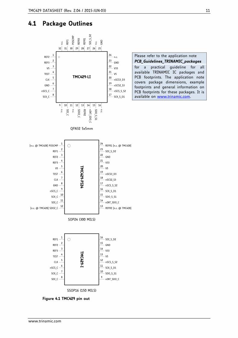
4.1 Package Outlines
TMC429-I
V33
nSCS_C
GND
SDI_C
TEST V5
SCK_C
SDI_S_D2
nINT_SDO_C
CLK nSCS_S_S2
REF2
REF1
REF3
SCK_S_D1
SDO_S_S1
1
2
3
4
5
6
7
8
16
10
11
12
13
14
15
9
SSOP16 (150 MILS)
TMC429-PI24
V33
nSCS_C
GND
SDI_C
TEST
V5
SCK_C
SDI_S_D2
nINT_SDO_C
CLK
nSCS_S_S2
REF2
REF1
REF3
SCK_S_D1
SDO_S_S1
3
4
5
6
7
8
9
10
23
15
16
17
20
21
22
14
1
2
11
12
24
13
18nSCS2_S3
19nSCS3_D3
SOP24 (300 MILS)
V5
GND
REFR1 [n.c. @ TMC428]
REFR2 [n.c. @ TMC428]
[n.c. @ TMC428] POSCMP
[n.c. @ TMC428] SDOZ_C
TMC429-LI
nSCS_C
TEST
SCK_C
CLK
REF2
REF3
3
4
5
6
7
8
9
1
2
QFN32 5x5mm
V5
GND
n.c.
10 11 12 13 14 15 16
32 31 30 29 28 27 26 25
22
21
20
19
18
17
24
23
REF1
n.c.
SDI_C
n.c.
SDOZ_C
REFR2
nIN
T_SDO_C
SDO_S_S1
n.c.
SCK_S_D1
nSCS_S_S2
nSCS2_S3
nSCS3_D3
V5
V33
GND
n.c.
SDI_
S_D2
REFR
1
REFR
3
POSC
MP
GND
n.c.
Figure 4.1 TMC429 pin out
Please refer to the application note PCB_Guidelines_TRINAMIC_packages for a practical guideline for all available TRINAMIC IC packages and PCB footprints. The application note covers package dimensions, example footprints and general information on PCB footprints for these packages. It is available on www.trinamic.com.
TMC429 DATASHEET (Rev. 2.04 / 2015-JUN-03) 12
www.trinamic.com
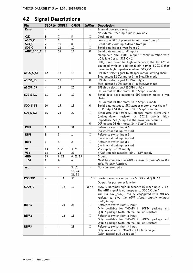
4.2 Signal Descriptions Pin SSOP16 SOP24 QFN32 In/Out Description Reset - - - - Internal power-on reset.
No external reset input pin is available. CLK 5 7 5 I Clock input nSCS_C 6 9 7 I Low active SPI chip select input driven from µC SCK_C 7 10 8 I Serial data clock input driven from µC SDI_C 8 11 10 I Serial data input driven from µC nINT_SDO_C
9 14 14 O Serial data output to µC input / Multiplexed nINTERRUPT output if communication with µC is idle (resp. nSCS_C = 1) SDO_C will never be high impedance; the TMC429 is equipped with an additional pin named SDOZ_C that becomes high impedance when nSCS_C=1.
nSCS_S_S2
12 17 18 O SPI chip select signal to stepper motor driving chain Step output S2 (for motor 2) in Step/Dir mode
nSCS2_S3
- 18 19 O SPI chip select signal (SOP24 only) / Step output S3 (for motor 3) in Step/Dir mode
nSCS3_D3
- 19 20 O SPI chip select signal (SOP24 only) / DIR output D3 (for motor 3) in Step/Dir mode
SCK_S_D1
11 16 17 O Serial data clock output to SPI stepper motor driver chain / DIR output D1 (for motor 1) in Step/Dir mode
SDO_S_S1
10 15 15 O Serial data output to SPI stepper motor driver chain / STEP output S1 (for motor 1) in Step/Dir mode
SDI_S_D2
16 23 27 I O
Serial data input from SPI stepper motor driver chain (pull-up/-down resistor at SDI_S avoids high impedance; SDI_S input is the power-on default) / DIR output D2 (for motor 2) in Step/Dir mode
REF1 1 2 31 I Reference switch input 1 (no internal pull-up resistor)
REF2 2 3 1 I Reference switch input 2 (no internal pull-up resistor)
REF3 3 4 2 I Reference switch input 3 (no internal pull-up resistor)
V5 13 5, 20 3, 21 +5V supply / +3.3V supply V33 14 21 22 470nF ceramic capacitor pin / +3.3V supply GND 15 8, 22 6, 23, 25 Ground TEST 4 6 4 I Must be connected to GND as close as possible to the
chip. No user function. n.c. - - 9, 11,
16, 24, 26, 32
- Not connected pins
POSCMP
- 1 30 n.c. / O Position compare output for SOP24 and QFN32 /
Output for pos_comp function
SDOZ_C - 12 12 O / Z SDOZ_C becomes high impedance (Z) when nSCS_C=1 / The nINT signal is not mapped to SDOZ_C pin / The pin nINT_SDO_C can be configured with TMC429 register to give the nINT signal directly without multiplexing
REFR1 - 24 28 I Reference switch right 1 input Only available for TMC429 in SOP24 package and QFN32 package (with internal pull-up resistor)
REFR2 - 13 13 I Reference switch right 2 input Only available for TMC429 in SOP24 package and QFN32 package (with internal pull-up resistor)
REFR3 - - 29 I Reference switch right 3 input Only available for TMC429 in QFN32 package (with internal pull-up resistor)

TMC429 DATASHEET (Rev. 2.04 / 2015-JUN-03) 13
www.trinamic.com
5 Sample Circuits The sample circuits show the connection of the external components.
5.1 Application Example: TMC429 in QFN32 Package All signals of the TMC429 are available with the QFN32 package. We recommend this package for applications using TRINAMICs TMC26x smart power driver family.
SCK_S_D1
SDO_S_S1
SDI_S_D2
nSCS_S_S2
REF2 REF3REF1
TEST GND
SDI_C
nSCS_C
SCK_C
nINT_SDO_C
CLK V5V33
TMC429-LI
nSCS3_D3
nSCS2_S3
POSCMP
REFR3REFR2REFR1
SDOZ_C
STP_3
DIR_3
STP_2
DIR_2
STP_1
DIR_1
MISO
MOSI
SCK
nSCS
µC
TMC26x
TMC26x
TMC26x
Figure 5.1 TMC429 within QFN32 package
STEP
DIR
CSN
SCK
SDI
SDO
TMC26x #1
STEP
DIR
CSN
SCK
SDI
SDO
TMC26x #2
STEP
DIR
CSN
SCK
SDI
SDO
TMC26x #3
nSCS2_S3
nSCS3_D3
nSCS_S_S2
SDI_S_D2
SDO_S_S1
SCK_S_D1
nSCS_C
SCK_C
SDI_C
SDOZ_C
MOSIMISO
SCK
TMC429-LI
CSn_0
CSn_1CSn_2CSn_3
CLKCLK
100K
Figure 5.2 TMC429 / TMC26x outline for configuration via SPI and STEP/DIR for motion
APPLICATION ENVIRONMENT OF TMC429 (QFN32 PACKAGE) AND 3 X TMC26X STEPPER MOTOR DRIVER: - One SPI chip select signal CSN_0 selects the TMC429 SPI microcontroller interface. - Up to three SPI chip select signals (CSN_3, CSN_2, CSN1) select up to three TMC262 SPI for
configuration. - The TMC429 SDOZ_C is high impedance when nSCS_C is 1.

TMC429 DATASHEET (Rev. 2.04 / 2015-JUN-03) 14
www.trinamic.com
5.2 Application Example: TMC429 in SSOP16 Package The low-prized TMC429-I is an optimum choice for SPI stepper motor drivers if the additional functions of the TMC429-LI are not required. We recommend this package for TRINAMICs TMC23x and TMC24x stepper driver family.
10K
SCK_S
SDO_S
SDI_S
nSCS_S
SDOCSN
SDI
SCK
SDOCSN
SDI
SCK
SDOCSN
SDI
SCKTMC23x / TMC24x TMC23x / TMC24x TMC23x / TMC24x
REF2 REF3REF1
TEST GND
µC
SCK
MOSI
MISO
SS
SDI_C
nSCS_C
SCK_C
SDO_C
CLK
CLK V5V33
470 nF
+5 V
1K 1K
Reference Switch Inputs active high
SM#3 SM#2 SM#1
TMC429-LI
1K
100 nF
Output SDO_C will nerver be high impedance
10nF 10nF 10nF
4.7K
4.7K
4.7K
Optional filter for long cables and to avoid failure if switch wires are next to motor cables.
Figure 5.3 TMC429 application environment with TMC429 in SSOP16 package
5.3 Application Example: TMC429 with Drivers without Serial Data Output (SDO)
For driver chips without serial data output the TMC429-LI and the TMC429-PI24 with two additional chip select outputs are available. The TMC429 sends data to the driver chain on demand only, which minimizes the interface traffic and reduces the power consumption.
10K
SCK_S
SDO_S
SDI_S
nSCS_S
nSCSSDI
SCK
nSCSSDI
SCK
nSCSSDI
SCK
Driver w/ o SDO
Driverw/ o SDO
REF2 REF3REF1
TEST GND
µC
SCK
MOSI
MISO
SS
SDI_C
nSCS_C
SCK_C
SDO_C/SDOZ_C
CLK
CLK V5V33
470 nF
+ 5 V
SM#3 SM#2 SM#1
TMC429- LI / TMC429-PI24
nSCS2
nSCS3
V5 GND
Output SDO_ C will nerver be high impedance
Driverw/ o SDO
REFR1 REFR2 REFR3
Figure 5.4 Usage of drivers without serial data output (SDO) with TMC429 in SOP24 or in QFN32 packages

TMC429 DATASHEET (Rev. 2.04 / 2015-JUN-03) 15
www.trinamic.com
6 Control Interface The communication takes place via four wire serial interfaces and 32 bit datagrams of fixed length. Stepper motor drivers with parallel inputs can be used in connection with the TMC429 with some additional glue logic.
RESPONSIBILITIES ARE DEFINED AS FOLLOWS: - The microcontroller is master of the TMC429. - The TMC429 is master of the stepper motor driver daisy chain.
AUTOMATIC POWER-ON RESET: - The TMC429 cannot be accessed before the power-on reset is completed and the clock is stable. - All register bits are initialized with 0 during power-on-reset, except the SPI clock pre-divider
clk2_div that is initialized with 15 (see section 8.2.5.3).
6.1 Bus Signals Signal Description TMC429 Microcontroller
Bus clock input SCK_C Serial data input SDI_C Serial data output SDO_C Chip select input nSCS_C
6.2 Serial Peripheral Interface for µC The serial microcontroller interface of the TMC429 acts as a 32 bit shift register.
COMMUNICATION BETWEEN µC AND THE TMC429 1. The serial µC interface shifts serial data into SDI_C with each rising edge of the clock signal
SCK_C. 2. Then, it copies the content of the 32 bit shift register into a buffer register with the rising
edge of the selection signal nSCS_C. 3. The serial interface of the TMC429 immediately sends back data read from registers or read
from internal RAM via the signal SDO_C. 4. The signal SDO_C can be sampled with the rising edge of SCK_C. SDO_C becomes valid at
least four CLK clock cycles after SCK_C becomes low as outlined in the timing diagram.
6.2.1 Timing A complete serial datagram frame has a fixed length of 32 bit. Because of on-the-fly processing of the input data stream, the serial µC interface of the TMC429 requires the serial data clock signal SCK_C to have a minimum low / high time of three clock cycles. The SPI signals from the µC interface may be asynchronous to the clock signal CLK of the TMC429. If the microcontroller and the TMC429 work on different clock domains that run asynchronously by the timing of the SPI interface of the microcontroller should be made conservative in the way that the length of one SPI clock cycle equals 8 or more clock cycles of the TMC429 clock CLK.

TMC429 DATASHEET (Rev. 2.04 / 2015-JUN-03) 16
www.trinamic.com
tSDtSD
CLK
sdi_c_bit#31
tSCKCL tSCKCHtSUCSC tHDCSC
1 x SDI_C sampled
one full 32 bit datagram
SDO_C(for TMC429-I)
SDI_C
SCK_C
nSCS_C
sdi_c_bit#30 . . . sdi_c_bit#1
30 x sampled SDI_C
sdi_c_bit#0
1 x SDI_C sampled
tCLK
tDATAGRAMuC
tPDtIS
tSD
tSI
tHDCSC tSUCSC
sdo_c_bit#31 sdo_c_bit#30 ... sdo_c_bit#1 sdo_c_bit#0
nINT sdo_c_bit#31 sdo_c_bit#30 ... sdo_c_bit#1 sdo_c_bit#0 nINT
SDOZ_C
Figure 6.1 Timing diagram of the serial µC interface
EXPLANATORY NOTES - While the data transmission from the microcontroller to the TMC429 is idle, the low active serial
chip select input nSCS_C and also the serial data clock signal SCK_C are set to high. - While the signal nSCS_C is high, the TMC429 assigns the status of the internal low active
interrupt signal nINT to the serial data output SDO_C. - The data signal SDI_C driven by the microcontroller has to be valid at the rising edge of the
serial data clock input SCK_C. The maximum duration of the serial data clock period is unlimited. - While the µC interface of the TMC429 is idle, the SDO_C signal is the (active low) interrupt status
nINT of the integrated interrupt controller of the TMC429. The timing of the multiplexed interrupt status signal nINT is characterized by the parameters tIS and tSI (see chapter 16.3).
The following SPI clock frequencies are recommended in order to avoid possible issues concerning the SPI frequency between microcontroller and TMC429: - For fCLK = 16MHz an upper SPI clock frequency of 1MHz is recommended. - For fCLK = 32MHz an upper SPI clock frequency of 2MHz is recommended.
PROCEDURE OF DATA TRANSMISSION 1. The signal nSCS_C has to be high for at least three clock cycles before starting a datagram
transmission. To initiate a transmission, the signal nSCS_C has to be set to low. 2. Three clock cycles later the serial data clock may go low. 3. The most significant bit (MSB) of a 32 bit wide datagram comes first and the least significant
bit (LSB) is transmitted as the last one. 4. A data transmission is finished by setting nSCS_C high three or more CLK cycles after the last
rising SCK_C slope. 5. So, nSCS_C and SCK_C change in opposite order from low to high at the end of a data
transmission as these signals change from high to low at the beginning. Information for TMC429-I / 16-pin package In contrast to most other SPI compatible devices, the serial data output SDO_C of the TMC429-I is always driven. It will never be high impedance Z. If high impedance is required for the SDO_C connected to the microcontroller, it can be realized using a single gate 74HCT1G125. An additional pin named SDOZ_C is available for the TMC429 with an integrated high impedance driver.
TMC429 DATASHEET (Rev. 2.04 / 2015-JUN-03) 17
www.trinamic.com
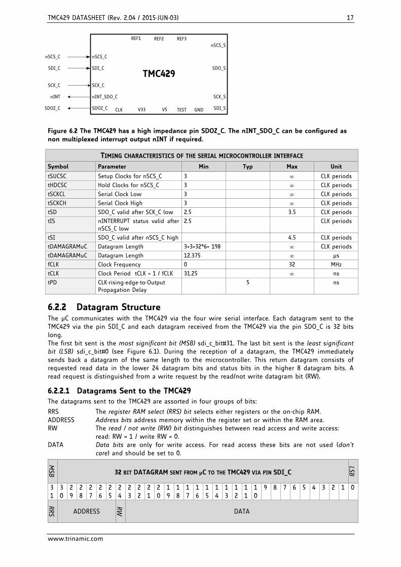
SCK_S
SDO_S
SDI_S
nSCS_SREF2 REF3REF1
TEST GNDCLK V5V33
TMC429SCK_C
SDI_C
nSCS_C
SDOZ_C
SCK_C
SDI_C
nSCS_C
SDOZ_C
nINT_SDO_CnINT
Figure 6.2 The TMC429 has a high impedance pin SDOZ_C. The nINT_SDO_C can be configured as non multiplexed interrupt output nINT if required.
TIMING CHARACTERISTICS OF THE SERIAL MICROCONTROLLER INTERFACE Symbol Parameter Min Typ Max Unit
tSUCSC Setup Clocks for nSCS_C 3 ∞ CLK periods
tHDCSC Hold Clocks for nSCS_C 3 ∞ CLK periods
tSCKCL Serial Clock Low 3 ∞ CLK periods
tSCKCH Serial Clock High 3 ∞ CLK periods
tSD SDO_C valid after SCK_C low 2.5 3.5 CLK periods
tIS nINTERRUPT status valid after nSCS_C low
2.5 CLK periods
tSI SDO_C valid after nSCS_C high 4.5 CLK periods
tDAMAGRAMuC Datagram Length 3+3+32*6= 198 ∞ CLK periods
tDAMAGRAMuC Datagram Length 12.375 ∞ µs
fCLK Clock Frequency 0 32 MHz
tCLK Clock Period tCLK = 1 / fCLK 31.25 ∞ ns
tPD CLK-rising-edge-to-Output Propagation Delay
5 ns
6.2.2 Datagram Structure The µC communicates with the TMC429 via the four wire serial interface. Each datagram sent to the TMC429 via the pin SDI_C and each datagram received from the TMC429 via the pin SDO_C is 32 bits long. The first bit sent is the most significant bit (MSB) sdi_c_bit#31. The last bit sent is the least significant bit (LSB) sdi_c_bit#0 (see Figure 6.1). During the reception of a datagram, the TMC429 immediately sends back a datagram of the same length to the microcontroller. This return datagram consists of requested read data in the lower 24 datagram bits and status bits in the higher 8 datagram bits. A read request is distinguished from a write request by the read/not write datagram bit (RW).
6.2.2.1 Datagrams Sent to the TMC429 The datagrams sent to the TMC429 are assorted in four groups of bits:
RRS The register RAM select (RRS) bit selects either registers or the on-chip RAM. ADDRESS Address bits address memory within the register set or within the RAM area. RW The read / not write (RW) bit distinguishes between read access and write access:
read: RW = 1 / write RW = 0. DATA Data bits are only for write access. For read access these bits are not used (don’t
care) and should be set to 0.
MSB
32 BIT DATAGRAM SENT FROM µC TO THE TMC429 VIA PIN SDI_C
LSB
31
30
29
28
27
26
25
24
23
22
21
20
19
18
17
16
15
14
13
12
11
10
9 8 7 6 5 4 3 2 1 0
RRS ADDRESS
RW DATA
TMC429 DATASHEET (Rev. 2.04 / 2015-JUN-03) 18
www.trinamic.com
NOTE - Different internal registers of the TMC429 have different lengths. For some registers only a subset
of 24 data bits is used. - Unused data bits should be set to 0. - Some addresses select a couple of registers mapped together into the 24 data bit space.
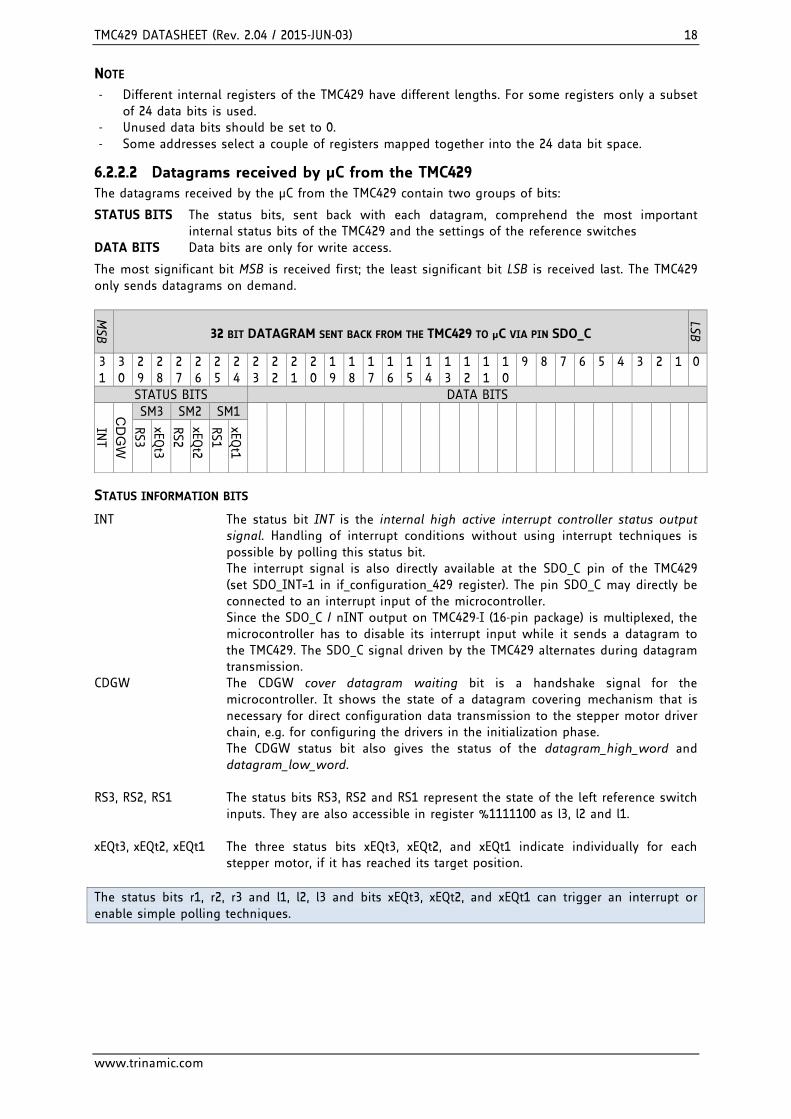
6.2.2.2 Datagrams received by µC from the TMC429 The datagrams received by the µC from the TMC429 contain two groups of bits:
STATUS BITS The status bits, sent back with each datagram, comprehend the most important internal status bits of the TMC429 and the settings of the reference switches
DATA BITS Data bits are only for write access.
The most significant bit MSB is received first; the least significant bit LSB is received last. The TMC429 only sends datagrams on demand.
MSB
32 BIT DATAGRAM SENT BACK FROM THE TMC429 TO µC VIA PIN SDO_C
LSB
31
30
29
28
27
26
25
24
23
22
21
20
19
18
17
16
15
14
13
12
11
10
9 8 7 6 5 4 3 2 1 0
STATUS BITS DATA BITS
INT
CD
GW
SM3 SM2 SM1
RS3
xEQt3
RS2
xEQt2
RS1
xEQt1
STATUS INFORMATION BITS
INT The status bit INT is the internal high active interrupt controller status output signal. Handling of interrupt conditions without using interrupt techniques is possible by polling this status bit.
The interrupt signal is also directly available at the SDO_C pin of the TMC429 (set SDO_INT=1 in if_configuration_429 register). The pin SDO_C may directly be connected to an interrupt input of the microcontroller.
Since the SDO_C / nINT output on TMC429-I (16-pin package) is multiplexed, the microcontroller has to disable its interrupt input while it sends a datagram to the TMC429. The SDO_C signal driven by the TMC429 alternates during datagram transmission.
CDGW The CDGW cover datagram waiting bit is a handshake signal for the microcontroller. It shows the state of a datagram covering mechanism that is necessary for direct configuration data transmission to the stepper motor driver chain, e.g. for configuring the drivers in the initialization phase.
The CDGW status bit also gives the status of the datagram_high_word and datagram_low_word.
RS3, RS2, RS1 The status bits RS3, RS2 and RS1 represent the state of the left reference switch
inputs. They are also accessible in register %1111100 as l3, l2 and l1. xEQt3, xEQt2, xEQt1 The three status bits xEQt3, xEQt2, and xEQt1 indicate individually for each
stepper motor, if it has reached its target position. The status bits r1, r2, r3 and l1, l2, l3 and bits xEQt3, xEQt2, and xEQt1 can trigger an interrupt or enable simple polling techniques.

TMC429 DATASHEET (Rev. 2.04 / 2015-JUN-03) 19
www.trinamic.com
6.2.3 Simple Datagram Examples The % prefix – normally indicating binary representation in this data sheet – is omitted for the following datagram examples. Assuming, one would like to write (RW=0) to a register (RRS=0) at the address %001101 the following data word %0000 0000 0000 0001 0010 0011, one would have to send the following 32 bit datagram 00011010000000000000000100100011 to the TMC429. With inactive interrupt (INT=0), no cover datagram waiting (CDGW=0), all reference switches inactive (RS3=0, RS2=0, RS1=0), and all stepper motors at target position (xEQt3=1, xEQt2=1, xEQt1=1) the status bits would be %10010101 the TMC429 would send back the 32 bit datagram: 10010101000000000000000000000000 To read (RW=1) back the register written before, one would have to send the 32 bit datagram 00011011000000000000000000000000 to the TMC429 and the TMC429 would reply with the datagram 10010101000000000000000100100011. Write (RW=0) access to on-chip RAM (RRS=1) to an address %111111 occurs similar to register access, but with RRS=1. To write two 6 bit data words %100001 and %100011 to successive pair-wise RAM addresses %1111110 and %1111111 (%100001 to %1111110 and %100011 to %1111111) which are commonly addressed by one datagram, one would have to send the datagram 11111110000000000010001100100001. To read (rw=1) from that on-chip memory address, one would have to send the datagram 11111111000000000000000000000000.

TMC429 DATASHEET (Rev. 2.04 / 2015-JUN-03) 20
www.trinamic.com
7 Address Space Partitions The functionality of the TMC429 is mapped to registers which are combined to groups and mapped to the address space: - Each stepper motor has a set of registers individually assigned to it and arranged within a
contiguous address space. - A set of registers within the address space holds the global parameters which are common for
all stepper motors. A single dedicated global parameter register is essential for the configuration of the serial four wire stepper motor driver interface.
- One half of the on-chip RAM address space holds the configuration parameters for the stepper motor driver chain (used for SPI mode, only).
- The other half of the on-chip RAM address space is provided to store a microstep table if required (used for SPI mode, only).
- The first seven datagram bits (sdi_c_bit#31 and sdi_c_bit#30 ... sdi_c_bit#25, respectively RRS and ADDRESS) address the whole address space of the TMC429.
ADDRESS SPACE PARTITIONS
Address ranges (incl. RRS) Assignment
%000 0000 . . . %000 1111 16 registers for stepper motor #1
Registers with up to 24 bits
%001 0000 . . . %001 1111 16 registers for stepper motor #2
%010 0000 . . . %010 1111 16 registers for stepper motor #3
%011 0000 . . . %011 1110 15 common registers
%011 1111 1 global parameter register
%100 0000 . . . %101 1111 32 addresses of 2x6 bit for driver chain configuration RAM 128x6 bit %110 0000 . . . %111 1111 32 addresses of 2x6 bit for microstep table
CHANGING TARGET POSITION OR TARGET VELOCITY OF SINGLE MOTORS The stepper motors are controlled directly by writing motion parameters into associated registers. Only one register write access is necessary for changing a target motion parameter. Thus the microcontroller has to send one 32 bit datagram to the TMC429 for altering the target position or the target velocity of one stepper motor.
CHANGING DRIVER CONFIGURATION OR MICROSTEP TABLE OF ALL MOTORS Some parameters are packed together in a single data word at a single address. These parameters have to be initialized once and remain unchanged during operation. They have to be changed in common. The access to the on-chip RAM addresses concern two successive RAM addresses. So, always two data words are modified with each write access to the on-chip RAM. Once initialized after power-up, the content of the RAM is usually left unchanged.
7.1 Read and Write Read and write access is selected by the RW bit (sdi_c_bit#24) of the datagram sent from the µC to the TMC429. The on-chip configuration RAM and the registers are writeable with read-back option. Some addresses are read-only. Write access (RW=0) to some of those read-only registers triggers additional functions, explained in detail later.
7.2 Register Set The register address mapping is given in chapter 7.3. The registers are initialized internally during power-up. During power-up initialization, the TMC429 does not send any datagrams to the stepper motor driver chain. The TMC429 loads a default RAM configuration for a TMC236 / TMC239 / TMC246 / TMC249 SPI driver chain on power-on reset. For a Step/Dir driver chain this is of no relevance.

TMC429 DATASHEET (Rev. 2.04 / 2015-JUN-03) 21
www.trinamic.com
7.3 Register Mapping All register bits are initialized with 0 during power on reset, except the SPI clock pre-divider clk2_div (see section 8.2.5.3) that is initialized with 15. The on-chip RAM of the TMC429 is initialized internally during power-up. It can be modified by the microcontroller as required.
TMC429 REGISTER MAPPING
32 BIT DATAGRAM SENT FROM µC TO THE TMC429 VIA PIN SDI_C
31
30
29
28
27
26
25
24
23
22
21
20
19
18
17
16
15
14
13
12
11
10
9 8 7 6 5 4 3 2 1 0
RRS ADDRESS
RW
DATA
0
SMDA IDX
RW=0 : W
RITE access / RW=1 : REA
D access
THREE STEPPER MOTOR REGISTER SETS (SMDA=00, 01, 10)
0 0 1
0 1 0
0 0 0 0 X_TARGET 0 0 0 1 X_ACTUAL 0 0 1 0 V_MIN 0 0 1 1 V_MAX 0 1 0 0 V_TARGET 0 1 0 1 V_ACTUAL 0 1 1 0 A_MAX 0 1 1 1 A_ACTUAL 1 0 0 0 IS_AGTAT IS_ALEAT IS_v0 A_THRESHOLD 1 0 0 1 1 PMUL PDIV 1 0 1 0 lp REF_CONF R_M 1 0 1 1 INTERRUPT_MASK INTERRUPF_FLAGS 1 1 0 0 PULSE_DIV RAMP_DIV USRS 1 1 0 1 DX_REF_TOLERANCE 1 1 1 0 X_LATCHED
1 1 1 1 USTEP_COUNT_429
1 1
JDX COMMON REGISTERS (SMDA=11) 0 0 0 0 DATAGRAM_LOW_WORD 0 0 0 1 DATAGRAM_HIGH_WORD 0 0 1 0 cw COVER_POSITION COVER_LEN 0 0 1 1 COVER_DATAGRAM 0 1 0 0 IF_CONFIGURATION_429 0 1 0 1 POS_COMP_429 0 1 1 0 POS_COMP_INT_429 M I 1 0 0 0 POWER-DOWN 1 0 0 1 TYPE_VERSION_429 (= $429101 for TMC429 version 1.01, read-only) 1 1 1 0 l3 r3 l2 r2 l1 r1
1 1 1 1 1 1
mot1r
refmux
cont_upd
ate
CLK2_DIV
cs_Com
Ind
POLARITIES
LSMD
dac_ab
fd_ab
ph_ab
sck_s
nscs_s 0 0 0 0 STPDIV_429
(if en_sd=1)
SMDA = stepper motor driver address M = mask R_M = RAMP_MODE I = interrupt cw = cover waiting RRS = register RAM select l1, l2, l3 = left switch 1/2/3 (read-out) r1, r2, r3 = right switch 1/2/3 (read-out)
unused bits

TMC429 DATASHEET (Rev. 2.04 / 2015-JUN-03) 22
www.trinamic.com
8 Register Description The TMC429 provides axis parameter registers and global parameter registers.
8.1 Axis Parameter Registers The registers hold binary coded numbers. Some are unsigned (positive) numbers, some are signed numbers in two’s complement, and some are control bits or single flags. The functionality of different registers depends on the RAMP_MODE (refer to chapter 8.1.11).
OVERVIEW AXIS PARAMETER REGISTER MAPPING
REGISTER R / W TYPE DESCRIPTION X_TARGET R/W 24 bit This register holds the current target position in units of
microsteps. Positions can be treated as signed or unsigned. X_ACTUAL R/W*2 24 bit The current position of each stepper motor is available by read
out of this register. Positions can be treated as signed or unsigned.
V_MIN R/W 11 bit unsigned
This register holds the absolute velocity value at or below which the stepper motor can be stopped abruptly.
V_MAX R/W 11 bit unsigned
This parameter sets the maximum motor velocity.
V_TARGET R/W 12 bit signed The V_TARGET register holds the current target velocity. The use of V_TARGET depends on the chosen mode of operation.
V_ACTUAL R*1 12 bit signed This read-only register holds the current velocity of the associated stepper motor.
A_MAX R/W 11 bit unsigned
This register defines the absolute value of the desired acceleration for velocity_mode and ramp_mode (resp. soft_mode) with a value range from 0 to 2047.
A_ACTUAL R 12 bit signed The actual acceleration can be read out by the microcontroller from the A_ACTUAL read-only register.
IS_AGTAT IS_ALEAT IS_V0 A_THRESHOLD
R/W R/W R/W R/W
3 bit 3 bit 3 bit 11 bit unsigned
These parameters control the current scaling values IS in SPI driver mode. Depending on the ramp phase they are applied to the motor by scaling the amplitudes of the internal sequencer.
PMUL PDIV
R/W R/W
1+7 bit 4 bit unsigned
These values form a floating point number with PMUL as mantissa and PDIV as exponent. PMUL and PDIV are used for calculating the deceleration ramp.
RAMP_MODE REF_CONF lp
R/W R/W R
2 bit 4 bit 1 bit
The two bits RAMP_MODE (R_M) select one of the four possible modes of operation. The configuration bits REF_CONF select the behavior of the reference switches. The bit called lp (latched position) is a read only status bit.
INTERRUPT_MASK INTERRUPT_FLAGS
R/W R/W
8 bit 8 bit
The TMC429 provides one interrupt register of eight flags for each stepper motor.
RAMP_DIV PULSE_DIV USRS
R/W R/W R/W
4 bit 4 bit 2 bit
The parameter RAMP_DIV scales the acceleration parameter A_MAX. The pulse generator clock – defining the maximum step pulse rate – is determined by the parameter PULSE_DIV. The parameter PULSE_DIV scales the velocity parameters. The parameter USRS (µstep resolution selection) is used for setting the microstep resolution in SPI mode.
DX_REF_TOLERANCE R/W
12 bit DX_REF_TOLERANCE excludes a motion range to allow motion near the reference position.
X_LATCHED R 24 bit unsigned
This read-only register stores the actual position X_ACTUAL upon a change of the reference switch state.
USTEP_COUNT_429 R/W
8 bit The read-write register USTEP_COUNT_429 holds the actual microstep pointer of the internal sequencer.
*1 in hold_mode only, this register is a read-write register.
*2 before overwriting X_ACTUAL choose velocity_mode or hold_mode. Refer to chapter 8.1.2.

TMC429 DATASHEET (Rev. 2.04 / 2015-JUN-03) 23
www.trinamic.com
8.1.1 X_TARGET (IDX=%0000) This register holds the current target position in units of microsteps.
UNIT OF TARGET POSITION The unit of the target position depends on the setting of the associated microstep resolution register usrs.
POSITIONING - If the difference X_TARGET to X_ACTUAL is not zero and R_M = ramp_mode or soft_mode, the
TMC429 moves the stepper motor in the direction of X_TARGET in order to position X_ACTUAL to X_TARGET. Usually X_TARGET is modified to start a positioning.
- The condition | X_TARGET – X_ACTUAL | < 223 must be satisfied for motion into correct direction. - Target position X_TARGET and current position X_ACTUAL may be altered on the fly. - To move from one position to another, the ramp generator of the TMC429 automatically
generates ramp profiles in consideration of the velocity limits V_MIN and V_MAX and acceleration limit A_MAX.
The registers X_TARGET, X_ACTUAL, V_MIN, V_MAX, and A_MAX are initialized with zero after power up.
8.1.2 X_ACTUAL (IDX=%0001) The current position of each stepper motor is available by read out of the registers called X_ACTUAL. The actual position can be overwritten by the microcontroller. This feature is important for the reference switch position calibration controlled by the microcontroller.
UNIT OF CURRENT POSITION The unit of the target position depends on the setting of the associated microstep resolution register usrs. Attention Before overwriting X_ACTUAL choose velocity_mode or hold_mode. If X_ACTUAL is overwritten in ramp_mode or soft_mode the motor directly drives to X_TARGET.

TMC429 DATASHEET (Rev. 2.04 / 2015-JUN-03) 24
www.trinamic.com
8.1.3 V_MIN (IDX=%0010) This register holds the absolute velocity value at or below which the stepper motor can be stopped abruptly.
UNIT OF VELOCITY The unit of velocity parameters is steps per time unit. The scale of velocity parameters (V_MIN, V_MAX, V_TARGET, V_ACTUAL) is defined by the parameter PULSE_DIV (see page 8.1.13 for details) and depends on the clock frequency of the TMC429.
DECELERATION - The parameter V_MIN is relevant for deceleration while reaching a target position. V_MIN should
be set greater than zero. - This control value allows reaching the target position faster because the stepper motor is not
slowed down below V_MIN before the target is reached. - Due to the finite numerical representation of integral relations the target position cannot be
reached exactly, if the calculated velocity is less than one, before the target is reached. Setting V_MIN to at least one assures reaching each target position exactly.
t
v(t)
t0 t1
A_MAX
t3 t4t2
Δv
t7 t8t5
ΔvA_MAX
- A_MAX
- A_MAX
t6
acceleration constant velocity deceleration acceleration deceleration
Δt01 Δt56
Figure 8.1 Velocity ramp parameters and velocity profiles
8.1.4 V_MAX (IDX=%0011) This parameter sets the maximum motor velocity. The absolute value of the velocity will not exceed this limit, except if the limit V_MAX is changed during motion to a value below the current velocity.
UNIT OF VELOCITY The unit of velocity parameters is steps per time unit. The scale of velocity parameters (V_MIN, V_MAX, V_TARGET, V_ACTUAL) is defined by the parameter PULSE_DIV (see page 8.1.13 for details) and depends on the clock frequency of the TMC429.
HOMING PROCEDURE To set target position X_TARGET and current position X_ACTUAL to an equivalent value (e.g. to set both to zero at a reference point) the assigned stepper motor should be stopped first and the parameter V_MAX should be set to zero to hold the assigned stepper motor at rest before writing into the register X_TARGET and X_ACTUAL. Attention Before overwriting X_ACTUAL choose velocity_mode or hold_mode. If X_ACTUAL is overwritten in ramp_mode or soft_mode the motor directly drives to X_TARGET.

TMC429 DATASHEET (Rev. 2.04 / 2015-JUN-03) 25
www.trinamic.com
8.1.5 V_TARGET (IDX=%0100) The use of V_TARGET depends on the chosen mode of operation:
Mode of operation Functionality of V_TARGET
ramp_mode The V_TARGET register holds the current target velocity calculated internally by the ramp generator.
velocity_mode A target velocity can be written into the V_TARGET register. The associated stepper motor accelerates until it reaches the specified target velocity. The velocity is changed according to the motion parameter limits if the register V_TARGET is changed.
hold_mode The register V_TARGET is ignored. soft_mode The V_TARGET register holds the current target velocity calculated internally
by the ramp generator.
UNIT OF VELOCITY The unit of velocity parameters is steps per time unit. The scale of velocity parameters (V_MIN, V_MAX, V_TARGET, V_ACTUAL) is defined by the parameter PULSE_DIV (see chapter 8.1.13 for details) and depends on the clock frequency of the TMC429.
8.1.6 V_ACTUAL (IDX=%0101) This read-only register holds the current velocity of the associated stepper motor. Internally, the ramp generator of the TMC429 processes with 20 bits while only 12 bits (the most significant bits) can be read out as V_ACTUAL. In hold_mode only, this register is a read-write register. Writing zero to the register V_ACTUAL immediately stops the associated stepper motor, because hidden bits are set to zero with each write access to the register V_ACTUAL. In hold_mode motion parameters are ignored and the microcontroller has the full control to generate a ramp. The TMC429 only handles the microstepping and datagram generation for the associated stepper motor of the daisy chain.
UNIT The unit of velocity parameters is steps per time unit. The scale of velocity parameters (V_MIN, V_MAX, V_TARGET, and V_ACTUAL) is defined by the parameter PULSE_DIV (see chapter 8.1.13 for details) and depends on the clock frequency of the TMC429.
An actual velocity of zero read out by the microcontroller means that the current velocity is in an interval between zero and one. Therefore the actual velocity should not be used to detect a stop of a stepper motor. It is advised to detect the target_reached flag instead.
8.1.7 A_MAX (IDX=%0110) This register defines the absolute value of the desired acceleration for velocity_mode and ramp_mode (resp. soft_mode) with a value range from 0 to 2047.
Note The motion controller cannot stop the stepper motor if A_MAX is set to zero on the fly because afterwards the velocity cannot be changed automatically any more.
UNIT The unit of the acceleration is change of step frequency per time unit divided by 256. The scale of acceleration parameters (A_MAX, A_ACTUAL, and A_THRESHOLD) is defined by the parameter RAMP_DIV (see section 8.1.13) and depends on the clock frequency of the TMC429.
8.1.7.1 A_MAX in ramp_mode As long as RAMP_DIV ≥ PULSE_DIV – 1 is valid, any value of A_MAX within its range (0… 2047) is allowed and there exists a valid pair PMUL, PDIV for each A_MAX. The reason is that the acceleration scaling determined by RAMP_DIV is compatible with the step velocity scaling determined by PULSE_DIV. A large RAMP_DIV stands for low acceleration and a large PULSE_DIV stands for low velocity. Low acceleration is compatible with low speed and high speed as well, but high acceleration is more compatible with high speed.

TMC429 DATASHEET (Rev. 2.04 / 2015-JUN-03) 26
www.trinamic.com
Changing one parameter out of the triple A_MAX, RAMP_DIV, PULSE_DIV requires re-calculation of the parameter pair PMUL, PDIV to update the associated register. For description of the parameters PMUL and PDIV see section 8.1.10.
8.1.7.1.1 Deceleration in ramp_mode and soft_mode If RAMP_DIV and PULSE_DIV differ more than one while deceleration in ramp_mode or soft_mode the parameter A_MAX needs to have a lower limit (>1) and an upper limit (<2047). The reason is that the deceleration ramp is internally limited to 219 steps (respectively microsteps).
THE LOWER LIMIT OF A_MAX IS GIVEN BY
𝐴𝐴_𝑀𝑀𝐴𝐴𝑀𝑀𝐿𝐿𝐿𝐿𝐿𝐿𝐿𝐿𝐿𝐿_𝐿𝐿𝐿𝐿𝐿𝐿𝐿𝐿𝐿𝐿 = 2(𝐿𝐿𝑅𝑅𝐿𝐿𝑅𝑅_𝐷𝐷𝐿𝐿𝐷𝐷−𝑅𝑅𝑃𝑃𝐿𝐿𝑃𝑃𝐿𝐿_𝐷𝐷𝐿𝐿𝐷𝐷−1)
- With V_MAX set to 2048√2
(≈ 1448) or lower the A_MAXLOWER_LIMIT is half of this value.
- If RAMP_DIV – PULSE_DIV – 1 ≤ 0 the limit A_MAXLOWER_LIMIT is 1 and the parameter A_MAX may be set to 1.
THE UPPER LIMIT OF A_MAX IS GIVEN BY
𝐴𝐴_𝑀𝑀𝐴𝐴𝑀𝑀𝑃𝑃𝑅𝑅𝑅𝑅𝐿𝐿𝐿𝐿_𝐿𝐿𝐿𝐿𝐿𝐿𝐿𝐿𝐿𝐿 = 2(𝐿𝐿𝑅𝑅𝐿𝐿𝑅𝑅_𝐷𝐷𝐿𝐿𝐷𝐷−𝑅𝑅𝑃𝑃𝐿𝐿𝑃𝑃𝐿𝐿_𝐷𝐷𝐿𝐿𝐷𝐷+12) - 1
- If RAMP_DIV – PULSE_DIV + 1 ≥ 0 the A_MAX_UPPER_LIMIT is > 2048 and the parameter A_MAX might be set to any value up to 2047.
CONDITIONS The parameter A_MAX must not be set below A_MAXLOWER_LIMIT except A_MAX is set to 0. The condition A_MAX ≥ A_MAXLOWER_LIMIT as well as A_MAX ≤ A_MAXUPPER_LIMIT must be satisfied to reach any target position without oscillations. If that condition is not satisfied, oscillations around a target position may occur.
8.1.8 A_ACTUAL (IDX=%0111) The actual acceleration can be read out by the microcontroller from the A_ACTUAL read-only register. The actual acceleration is used to select scale factors for the coil currents. It is updated with each clock. The returned value A_ACTUAL is smoothed to avoid oscillations of the readout value. Thus, returned A_ACTUAL values should not be used directly for precise calculations.
UNIT The unit of the acceleration is change of step frequency per time unit divided by 256. The scale of acceleration parameters (A_MAX, A_ACTUAL, and A_THRESHOLD) is defined by the parameter RAMP_DIV (see section 8.1.13) and depends on the clock frequency of the TMC429.
8.1.9 IS_AGTAT, IS_ALEAT, IS_V0, and A_THRESHOLD (IDX=%1000) These parameters are only relevant in SPI mode. The parameters IS_AGTAT, IS_ALEAT, IS_V0, and A_THRESHOLD represent the current scaling values IS. Depending on the ramp phase they are applied to the motor by scaling the current amplitudes of the internal sequencer. The automatic motion dependent current scale feature of the TMC429 is provided primarily for microstep operation. It may also be applied for full step or half step drivers, if those provide current control bits. In this special case it is possible to initialize the microstep table with a constant function, square function or sine wave using the two most significant DAC bits.
IS_AGTAT The parameter IS_AGTAT is applied if the acceleration is greater than the threshold acceleration. This is used to increase current during acceleration phases.
IS_ALEAT The parameter IS_ALEAT is applied if the acceleration is lower than or equal to the threshold acceleration. This is the nominal motor current.
IS_V0 The third parameter IS_V0 is applied if the stepper motor is at rest. The parameter is used to save power, keep it cool, and avoid noise probably caused by chopper drivers.
A_THRESHOLD The parameter A_THRESHOLD is the threshold used for comparing with the current acceleration in order to select the current scale factor.

TMC429 DATASHEET (Rev. 2.04 / 2015-JUN-03) 27
www.trinamic.com
RELATIONSHIP BETWEEN IS_AGTAT, IS_ALEAT, AND IS_V0 AND THE INTERIM BIT VECTOR I_SCALE The parameters IS_AGTAT, IS_ALEAT, and IS_V0 are bit vectors of three bit width. One of these bit vectors is selected conditionally and assigned to the interim bit vector I_SCALE.
I_SCALE IS
0 0 0 1 = 100 % 0 0 1 1 / 8 = 12.5 % 0 1 0 2 / 8 = 25 % 0 1 1 3 / 8 = 37.5 % 1 0 0 4 / 8 = 50 % 1 0 1 5 / 8 = 62.5 % 1 1 0 6 / 8 = 75 % 1 1 1 7 / 8 = 87.5 %
NOTE - The maximum current scaling factor 1 is selected by I_SCALE = %000. This is the power-on
default. - The minimum current scaling factor 1/8 = 0.125 is selected by I_SCALE = %001. - The current scaling factor IS proportionally reduces the effective number of microsteps per full
step. For example, with I_SCALE = %100 (= 4/8 = 50%) the number of effective microsteps per full step is halved.
- When a low current scaling factor IS becomes used, the effective number of microsteps per full step may decrease, because less DAC steps are used to distinguish the same number of current levels. Therefore, it is advised to operate the application normally at 50% to 100% current scale.
The current scale selection scheme shows which of the scale factors IS_AGTAT, IS_ALEAT, and IS_V0 is selected corresponding to their conditions: If the velocity is zero, the parameter IS_V0 is used for scaling. If the velocity is not zero, either IS_ALEAT or IS_AGTAT is used for scaling. This depends on the absolute value of the acceleration and the acceleration threshold A_THRESHOLD.
CURRENT SCALE SELECTION SCHEME
Velocity value ATHRESHOLD value IS scale factor selection v= 0*1) IS := IS_V0*2)
v ≠ 0 ATHRESHOLD > 1023 IS := IS_ALEAT*3) | a | ≤ ATHRESHOLD IS := IS_ALEAT | a | > ATHRESHOLD IS := IS_AGTAT
*1) The configuration bit continuous_update of the stepper motor global parameter register must be set to 1 to make sure that the coil current is scaled for v=0 if all motors are at rest. The current scale for V=0 takes place delayed to avoid mechanical step loss due to oscillations of the motor after it has been stopped.
The delay time is: 𝑡𝑡𝐿𝐿𝑃𝑃_𝐷𝐷0_𝐷𝐷𝐿𝐿𝐿𝐿𝑅𝑅𝐷𝐷[𝑃𝑃] = 255×(32×2𝑅𝑅𝑅𝑅𝑅𝑅𝑅𝑅_𝐷𝐷𝐷𝐷𝐷𝐷 )𝑓𝑓𝐶𝐶𝐶𝐶𝐶𝐶[𝐻𝐻𝐻𝐻]
*2) For selection of current scaling IS_V0 (at rest) IS_AGTAT and IS_ALEAT must be larger than 0. *3) It is not advised to use A_THRESHOLD > 1023. Due to comparing of A_THRESHOLD with A_MAX a
setting of A_THRESHOLD with a value greater than 1023 results in using IS_ALEAT if A_MAX is greater than 1023 during acceleration.
For most applications setting IS_ALEAT and IS_AGTAT to the same value and using a lower value for IS_V0 is the best choice.

TMC429 DATASHEET (Rev. 2.04 / 2015-JUN-03) 28
www.trinamic.com
8.1.10 PMUL & PDIV (IDX=%1001) In ramp mode, the TMC429 uses an internal algorithm to calculate the deceleration ramp on the fly. This algorithm requires an additional proportionality factor P which allows the TMC429 to calculate the velocity required for stopping in time to exactly reach the target position without overshooting. This calculation is done for each ramp step. The result of this calculation can be read in the register V_TARGET. Whenever V_TARGET falls below the actual velocity, the TMC429 decelerates. As there is a large range of acceleration and velocity values, p is stored in a floating point representation, using the registers PMUL (mantissa) and PDIV (exponent). Using the proportionality factor P target positions are quickly reached without overshooting. The proportionality factor primarily depends on the acceleration limit A_MAX and on the two clock divider parameters PULSE_DIV and RAMP_DIV. These two separate clock divider parameters (set to the same value for most applications) provide an extremely wide dynamic range for acceleration and velocity. PULSE_DIV and RAMP_DIV allow reaching very high velocities with very low acceleration. Changing one parameter out of the triple A_MAX, RAMP_DIV, PULSE_DIV requires re-calculation of the parameter pair PMUL, PDIV to update the associated register.
8.1.10.1 Calculation of the Proportionality Factor p The representation of the proportionality factor p by the two parameters PMUL and PDIV is a floating point representation.
NOTATIONS Registers are PMUL and PDIV. Operating values are PMUL and PDIV.
CALCULATE P AS FOLLOWS:
𝑝𝑝 =𝑓𝑓𝐿𝐿𝑃𝑃𝐿𝐿𝑓𝑓𝐷𝐷𝐿𝐿𝐷𝐷
with PMUL = 128… 255 representing a factor of 1.000 to 1.992 (=1+127/128)
PDIV = 23, 24, 25… 214, 215, 216 PMUL ranges from 128 to 255. PDIV is a power of two with a range from 8 to 65536. Values of p less than 128 can be achieved by increasing PDIV.
The TMC429 does not directly store the PDIV parameter. The motion controller stores PDIV with
𝑓𝑓𝐷𝐷𝐿𝐿𝐷𝐷 = 23+𝑅𝑅𝐷𝐷𝐿𝐿𝐷𝐷
NOTE - Setting the factor p too small will result in a slow approach to the target position. - Setting the factor p too large will cause overshooting and even oscillations around the target
position. - The parameters PMUL and PDIV share the address IDX=%1001. The MSB of PMUL is fixed set to 1
and cannot be changed. This way, PMUL represents a mantissa in the range 1.000 (%1000 0000) to 1.992 (%1111 1111).
V_MAX
Target Position Calculation
Velocity Ramp Generator
(Micro-) Step pulsesV_TARGET
X_TARGET
X_ACTUAL
PDIVPMUL A_MAXV_MIN
PULSE_DIVRAMP_DIVclk32
CLOCK_DIV32clk
V_ACTUALPuls Generator
Figure 8.2 Target position calculation, ramp generator, and pulse generator

TMC429 DATASHEET (Rev. 2.04 / 2015-JUN-03) 29
www.trinamic.com
8.1.10.1.1 Calculation of p for a Given Acceleration p and the fitting PMUL and PDIV values can be calculated by the microcontroller. Optionally a pair of matching values of A_MAX, PMUL and PDIV can be stored into the microcontroller memory. The acceleration limit is a stepper motor parameter which is fixed in most applications. If the acceleration limit has to be changed nevertheless, the microcontroller can calculate a pair of PMUL and PDIV on demand for each new acceleration limit A_MAX with RAMP_DIV and PULSE_DIV. Also, pre-calculated pairs of PMUL and PDIV read from a table can be sufficient.
8.1.10.2 Calculation of PMUL and PDIV A pair of PMUL and PDIV has to be calculated for each provided acceleration limit A_MAX. Note, that there may be more than one valid pair of PMUL and PDIV for a given A_MAX acceleration limit.
CONSIDERATIONS FOR THE CALCULATION OF PMUL AND PDIV - To accelerate, the ramp generator accumulates the acceleration value to the actual velocity with
each time step. - The absolute value V_MAX of the velocity internally is represented by 11+8=19 bits, while only the
most significant 11 bits and the sign are used as input for the step pulse generator. So, there are 211=2048 values possible for specifying a velocity within a range of 0 to 2047.
- The ramp generator accumulates 1/256*A_MAX with each time step to the actual velocity value V_ACTUAL during acceleration phases. This accumulation uses 8 bits for decimals. So, the acceleration from a velocity V_ACTUAL=0 to the maximum possible velocity V_MAX=2047 spans over 2048*256 / A_MAX pulse generator clock pulses.
- Within the acceleration phase the pulse generator generates S = ½ * 2048* 256 / A_MAX * T steps for the (micro) step unit.
- The parameter T is the clock divider ratio: T = 2RAMP_DIV/ 2PULSE_DIV= 2RAMP_DIV– PULSE_DIV During the acceleration, the velocity has to be increased until the velocity limit V_MAX is reached or deceleration is required in order to exactly reach the target position. The TMC429 automatically determines the deceleration position in ramp_mode and decelerates. This calculation uses the difference between current position and target position and the proportionality parameter p, which has to be p = 2048 / S. The following formula results:
𝑝𝑝 =2048
12 ∗ 2048 ∗ 256
𝐴𝐴𝐿𝐿𝑅𝑅𝑀𝑀 ∗ 2𝐿𝐿𝑅𝑅𝐿𝐿𝑅𝑅_𝐷𝐷𝐿𝐿𝐷𝐷−𝑅𝑅𝑃𝑃𝐿𝐿𝑃𝑃𝐿𝐿_𝐷𝐷𝐿𝐿𝐷𝐷
This can be simplified to
𝑝𝑝 =𝐴𝐴_𝑀𝑀𝐴𝐴𝑀𝑀
128 ∗ 2𝐿𝐿𝑅𝑅𝐿𝐿𝑅𝑅_𝐷𝐷𝐿𝐿𝐷𝐷−𝑅𝑅𝑃𝑃𝐿𝐿𝑃𝑃𝐿𝐿_𝐷𝐷𝐿𝐿𝐷𝐷
HINTS - To avoid overshooting, the parameter PMUL should be made approximately 1% smaller than
calculated. Alternatively set p reduced by an amount of 1%. - If the proportionality parameter p is too small, the target position will be reached slower,
because the slow down ramp starts earlier. The target position is approached with minimal velocity V_MIN, whenever the internally calculated target velocity becomes less than V_MIN.
- With a good parameter p the minimal velocity V_MIN is reached a couple of steps before the target position.
- With parameter p set a little bit too large and a small V_MIN overshooting of one step (respectively one microstep) may occur. A decrement of the parameter PMUL avoids this one-step overshooting.

TMC429 DATASHEET (Rev. 2.04 / 2015-JUN-03) 30
www.trinamic.com
∆v
V_MAX
v(t)
V_MIN
p too small
p too large
p good
t1t0 t2
Figure 8.3 Proportionality parameter p and outline of velocity profile(s)
8.1.10.2.1 Choosing a Pair of PMUL and PDIV The calculation is based on the formula
𝑝𝑝 =𝑓𝑓𝐿𝐿𝑃𝑃𝐿𝐿𝑓𝑓𝐷𝐷𝐿𝐿𝐷𝐷
=𝑓𝑓𝑀𝑀𝑃𝑃𝑃𝑃
23+𝑅𝑅𝐷𝐷𝐿𝐿𝐷𝐷
CALCULATIONS 1. To represent the parameter p choose a pair of PMUL and PDIV which approximates p. 2. Value range for PMUL: 128… 255 3. Value range for PDIV: one out of 0, 1, 2, 3, 4, 5, 6, 7, 8, 9, 10, 11, 12, 13 (representing PDIV
one out of 8, 16, 32, 64, 128, 256, 512, 1024, 2048, 4096, 8192, 16384, 32786, 65536) 4. Try all 128 * 14 = 1792 possible pairs of PMUL and PDIV with a program and choose a matching
pair. 5. To find a pair, calculate for each pair of PMUL and PDIV
𝑝𝑝 = 𝑅𝑅_𝐿𝐿𝑅𝑅𝑀𝑀128∗2𝑅𝑅𝑅𝑅𝑅𝑅𝑅𝑅_𝐷𝐷𝐷𝐷𝐷𝐷−𝑅𝑅𝑃𝑃𝐶𝐶𝑃𝑃𝑃𝑃_𝐷𝐷𝐷𝐷𝐷𝐷 and
𝑝𝑝′ = 𝑅𝑅𝑅𝑅𝑃𝑃𝐶𝐶𝑅𝑅𝐷𝐷𝐷𝐷𝐷𝐷
= 𝑅𝑅𝐿𝐿𝑃𝑃𝐿𝐿23+𝑅𝑅𝐷𝐷𝐷𝐷𝐷𝐷
and
𝑞𝑞 =𝑝𝑝′
𝑝𝑝
6. Select one of the pairs satisfying the condition 0.95 < q < 1.0. The value q interpreted as a function q(a_max, ramp_div, pulse_div, pmul, pdiv) gives the quality criterion required.
Although q = 1.0 indicates that the chosen P_MUL and P_DIV perfectly represent the desired p factor for a given A_MAX, overshooting could result because of finite numerical precision. On the other hand in case of high resolution microstepping, overshooting of one microstep is negligible in most applications. To avoid overshooting, use P_MUL-1 instead of the selected P_MUL or select a pair (P_MUL, P_DIV) with q = 0.99.
8.1.10.2.2 Optimized Calculation of PMUL and PDIV The calculation of the parameters PMUL and PDIV can be simplified using the expression
𝑓𝑓𝑀𝑀𝑃𝑃𝑃𝑃 = 𝑝𝑝 ∗ 23 ∗ 2𝑅𝑅𝐷𝐷𝐿𝐿𝐷𝐷 with 𝑝𝑝 = 𝑅𝑅_𝐿𝐿𝑅𝑅𝑀𝑀128∗2𝑅𝑅𝑅𝑅𝑅𝑅𝑅𝑅_𝐷𝐷𝐷𝐷𝐷𝐷−𝑅𝑅𝑃𝑃𝐶𝐶𝑃𝑃𝑃𝑃_𝐷𝐷𝐷𝐷𝐷𝐷
To avoid overshooting, use
𝑝𝑝𝑟𝑟𝑟𝑟𝑟𝑟𝑟𝑟𝑟𝑟𝑟𝑟𝑟𝑟 = 𝑝𝑝 ∗ (1 − 𝑝𝑝𝑟𝑟𝑟𝑟𝑟𝑟𝑟𝑟𝑟𝑟𝑟𝑟𝑟𝑟𝑟𝑟𝑟𝑟[%]) with p_reduction approximately 1%
This results in:
𝑓𝑓𝑀𝑀𝑃𝑃𝑃𝑃 = 𝑝𝑝𝑟𝑟𝑟𝑟𝑟𝑟𝑟𝑟𝑟𝑟𝑟𝑟𝑟𝑟 ∗ 23 ∗ 2𝑅𝑅𝐷𝐷𝐿𝐿𝐷𝐷 = 0.99 ∗ 𝑝𝑝 ∗ 23 ∗ 2𝑅𝑅𝐷𝐷𝐿𝐿𝐷𝐷 PMUL becomes a function of the parameter PDIV. To find a valid pair PMUL, PDIV choose one out of 14 pairs for PDIV = 0, 1, 2, 3, ..., 13 with PMUL within the valid range 128 ≤ PMUL ≤ 255. The C language example pmulpdiv.c can be found on www.trinamic.com. The source code can directly be copied from the PDF datasheet file.

TMC429 DATASHEET (Rev. 2.04 / 2015-JUN-03) 31
www.trinamic.com
8.1.10.2.3 Calculation Example: PMUL and PDIV /* PROGRAM EXAMPLE ‘pmulpdiv.c’ : How to Calculate p_mul & p_div for the TMC429 */ #include <math.h> #include <stdio.h> #include <stdlib.h> #include <string.h> void CalcPMulPDiv(int a_max, int ramp_div, int pulse_div, float p_reduction, int *p_mul, int *p_div, double *PIdeal, double *PBest, double *PRedu ) int pdiv, pmul, pm, pd ; double p_ideal, p_best, p, p_reduced; pm=-1; pd=-1; // -1 indicates : no valid pair found p_ideal = a_max / (pow(2, ramp_div-pulse_div)*128.0); p = a_max / ( 128.0 * pow(2, ramp_div-pulse_div) ); p_reduced = p * ( 1.0 – p_reduction ); for (pdiv=0; pdiv<=13; pdiv++) pmul = (int)(p_reduced * 8.0 * pow(2, pdiv)) – 128; if ( (0 <= pmul) && (pmul <= 127) ) pm = pmul + 128; pd = pdiv; *p_mul = pm; *p_div = pd; p_best = ((double)(pm)) / ((double)pow(2,pd+3)); *PIdeal = p_ideal; *PBest = p_best; *PRedu = p_reduced; int main(int argc, char **argv) int a_max=0, ramp_div=0, pulse_div=0, p_mul, p_div, a_max_lower_limit=0, a_max_upper_limit=0; double pideal, pbest, predu; float p_reduction=0.0; char **argp; if (argc>1) while (argv++, argc--) argp = argv + 1; if (*argp==NULL) break; if ( (!strcmp(*argv,”-a”)) ) sscanf(*argp,”%d”,&a_max); else if ( (!strcmp(*argv,”-r”)) ) sscanf(*argp,”%d”,&ramp_div); else if ( (!strcmp(*argv,”-p”)) ) sscanf(*argp,”%d”,&pulse_div); else if ( (!strcmp(*argv,”-pr”))) sscanf(*argp,”%f”,&p_reduction); else fprintf(stderr,”\n USAGE : pmulpdiv –a <a_max> -r <ramp_div> -p <pulse_div> -pr <0.00 .. 0.10>\n” “ EXAMPLE : pmulpdiv –a 10 –r 3 –p 3 –pr 0.05\n”); return 1; printf(“\n\n a_max=%d\tramp_div=%d\tpulse_div=%d\tp_reduction=%f\n\n”, a_max, ramp_div, pulse_div, p_reduction); CalcPMulPDiv(a_max, ramp_div, pulse_div, p_reduction, &p_mul, &p_div, &pideal, &pbest, &predu ); printf(“ p_mul = %3.3d\n p_div = %3d\n\n p_ideal = %f\n p_best = %f\n p_redu = %f\n\n”, p_mul, p_div, pideal, pbest, predu); a_max_lower_limit = (int)pow(2,(ramp_div-pulse_div-1)); printf(“\n a_max_lower_limit = %d”,a_max_lower_limit); if (a_max < a_max_lower_limit) printf(“ [WARNING: a_max < a_max_lower_limit]”); a_max_upper_limit = ((int)pow(2,(12+(ramp_div-pulse_div)))) -1; printf(“\n a_max_upper_limit = %d”,a_max_upper_limit); if (a_max > a_max_upper_limit) printf(“ [WARNING: a_max > a_max_upper_limit]”); printf(“\n\n”); return 0; /* -------------------------------------------------------------------------- */
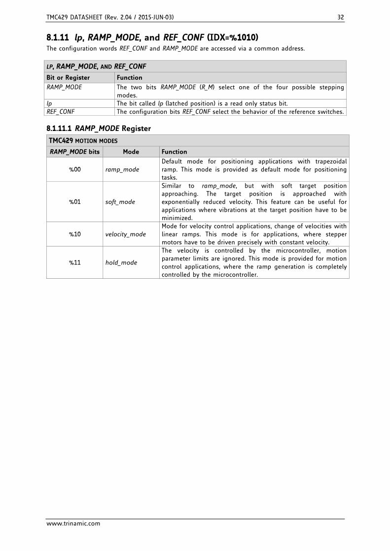
TMC429 DATASHEET (Rev. 2.04 / 2015-JUN-03) 32
www.trinamic.com
8.1.11 lp, RAMP_MODE, and REF_CONF (IDX=%1010) The configuration words REF_CONF and RAMP_MODE are accessed via a common address.
LP, RAMP_MODE, AND REF_CONF
Bit or Register Function
RAMP_MODE The two bits RAMP_MODE (R_M) select one of the four possible stepping modes.
lp The bit called lp (latched position) is a read only status bit. REF_CONF The configuration bits REF_CONF select the behavior of the reference switches.
8.1.11.1 RAMP_MODE Register
TMC429 MOTION MODES
RAMP_MODE bits Mode Function
%00 ramp_mode Default mode for positioning applications with trapezoidal ramp. This mode is provided as default mode for positioning tasks.
%01 soft_mode
Similar to ramp_mode, but with soft target position approaching. The target position is approached with exponentially reduced velocity. This feature can be useful for applications where vibrations at the target position have to be minimized.
%10 velocity_mode Mode for velocity control applications, change of velocities with linear ramps. This mode is for applications, where stepper motors have to be driven precisely with constant velocity.
%11 hold_mode
The velocity is controlled by the microcontroller, motion parameter limits are ignored. This mode is provided for motion control applications, where the ramp generation is completely controlled by the microcontroller.

TMC429 DATASHEET (Rev. 2.04 / 2015-JUN-03) 33
www.trinamic.com
8.1.11.2 The REF_CONF Register and the lp Read-Only Status Bit A reference switch can be used as an automatic stop switch. The reference switch indicates the reference position within a given tolerance. The automatic stop function of the switches can be enabled or disabled. Also a reference tolerance range (see register DX_REF_TOLERANCE, chapter 8.1.14) can be programmed to allow motion within the reference switch active range during homing. When a reference switch is triggered, the actual position can be stored automatically. This allows a precise determination of the reference point. It is initiated by writing a dummy value to the register X_LATCHED (see chapter 8.1.15). The read-only status bit lp (latch position waiting) indicates that the next change of the selected reference switch will trigger latching the position X_ACTUAL. The lp bit is automatically reset after position latching.
Negative direction
Mechanical inaccuracy of switches (switching hysteresis)
x1 x2
Motor
Traveller
Left switch
xleft
DX_REF_TOLERANCE
Positive direction
x3 x4xright
Right switch
xtraveler
Figure 8.4 Left switch and right switch for reference search and automatic stop function
The bits contained in the REF_CONF register control the semantic and the actions of the reference/stop switch modes for interrupt generation as explained later. The stepper motor stops if the reference/stop switch becomes active. This mechanism reacts only to the switch which corresponds to the actual motion direction, e.g. the right switch when moving to a more positive position. The configuration bits named disable_stop_l respectively disable_stop_r disable these automatic stop functions. If the bit soft_stop is set, the motor stops with linear ramp as determined by A_MAX.
REFERENCE SWITCH CONFIGURATION BITS REF_CONF AND LP STATUS BIT
REF_CONF mnemonic Function
disable_stop_l
0 : The motor will be stopped when the velocity is negative (V_ACTUAL < 0) and the left reference switch becomes active.
1 : Left reference switch is disabled as an automatic stop switch. disable_stop_r
0 : Stops a motor if the velocity is positive (V_ACTUAL > 0) and the right reference switch becomes active.
1 : Right reference switch is disabled as an automatic stop switch. soft_stop
0 : Stopping takes place immediately; motion parameter limits are ignored.
1 : Stopping takes place in consideration of motion parameter limits; stops with linear ramp.
ref_RnL
0 :
The bit ref_RnL (reference switch Right not Left) defines which switch will be used as the reference switch. The definition of the reference switch by the configuration bit ref_RnL has no effect on the stop function of the reference switches if disable_stop_l = 0 respectively disable_stop_r = 0. The left reference switch controls reference switch functions.
1 : The right (not left) reference switch controls reference switch functions.
lp
0 : This is the power-on default of the lp (latched position waiting) bit.
1 : X_LATCHED has been initialized by a write access to latch the position on a change of the reference switch. It is set to 0 after a position has been latched.
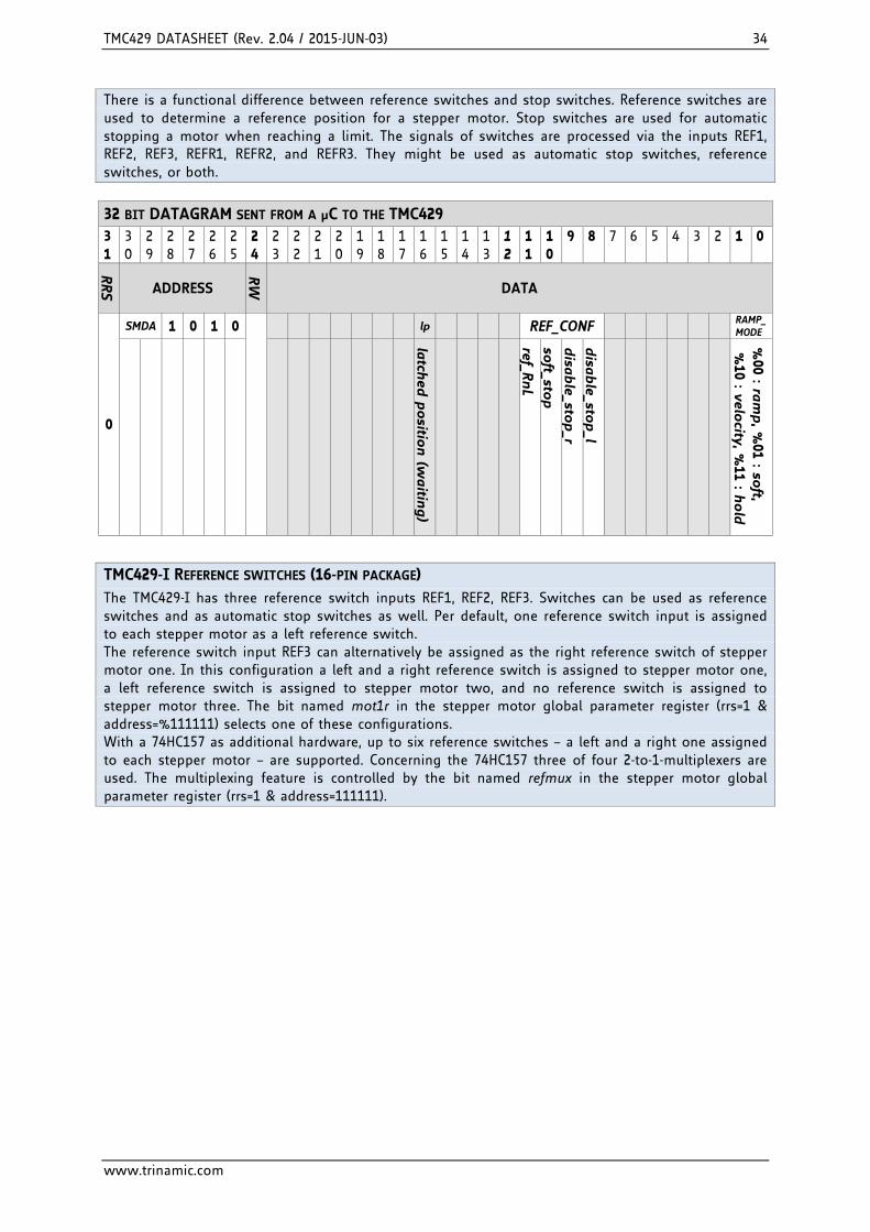
TMC429 DATASHEET (Rev. 2.04 / 2015-JUN-03) 34
www.trinamic.com
There is a functional difference between reference switches and stop switches. Reference switches are used to determine a reference position for a stepper motor. Stop switches are used for automatic stopping a motor when reaching a limit. The signals of switches are processed via the inputs REF1, REF2, REF3, REFR1, REFR2, and REFR3. They might be used as automatic stop switches, reference switches, or both.
32 BIT DATAGRAM SENT FROM A µC TO THE TMC429 31
30
29
28
27
26
25
24
23
22
21
20
19
18
17
16
15
14
13
12
11
10
9 8 7 6 5 4 3 2 1 0
RRS ADDRESS
RW
DATA
0
SMDA 1 0 1 0
lp REF_CONF RAMP_MODE
latch
ed p
ositio
n (w
aiting)
ref_RnL
soft_sto
p
disab
le_stop_r
disab
le_stop_l
%00 : ram
p, %
01 : soft,
%10 : velo
city, %11 : h
old
TMC429-I REFERENCE SWITCHES (16-PIN PACKAGE) The TMC429-I has three reference switch inputs REF1, REF2, REF3. Switches can be used as reference switches and as automatic stop switches as well. Per default, one reference switch input is assigned to each stepper motor as a left reference switch. The reference switch input REF3 can alternatively be assigned as the right reference switch of stepper motor one. In this configuration a left and a right reference switch is assigned to stepper motor one, a left reference switch is assigned to stepper motor two, and no reference switch is assigned to stepper motor three. The bit named mot1r in the stepper motor global parameter register (rrs=1 & address=%111111) selects one of these configurations. With a 74HC157 as additional hardware, up to six reference switches – a left and a right one assigned to each stepper motor – are supported. Concerning the 74HC157 three of four 2-to-1-multiplexers are used. The multiplexing feature is controlled by the bit named refmux in the stepper motor global parameter register (rrs=1 & address=111111).

TMC429 DATASHEET (Rev. 2.04 / 2015-JUN-03) 35
www.trinamic.com
8.1.12 INTERRUPT_MASK & INTERRUPT_FLAGS (IDX=%1011) The TMC429 provides one interrupt register of eight flags for each stepper motor. Interrupt bits are named int_<mnemonic>. The interrupt out nINT_SDO_C is set active low and the interrupt status bit int is set active high if at least one interrupt flag of one motor becomes set. If the interrupt status is inactive, nINT is high (1) and int is low (0).
SETTING MASKS AND FLAGS - An interrupt flag is set to 1 if its assigned interrupt condition occurs. - Each interrupt bit can either be enabled or disabled (1/0) individually by an associated interrupt
mask bit named mask_<mnemonic>. - Interrupt flags are reset to 0 by a write access (RW=0) to their interrupt register address
(IDX=%1011). Write 1 at the position of the bit to clear the flag. Writing a 0 to the corresponding position leaves the interrupt flag untouched.
- Interrupt flags are forced to 0 if the corresponding mask bit is disabled (0).
INTERRUPT FLAGS FOR EACH MOTOR
int_<mnemonic> Function
int_pos_end If a target position is reached while the interrupt mask mask_pos_end is 1, the bit is set to 1.
int_ref_wrong Reference switch signal was active outside the reference switch tolerance range (defined by the DX_REF_TOLERANCE register). The switches processed via the inputs REF1, REF2, REF3, REFR1, REFR2, and REFR3 can be used as stop switches for automatic motion limiting, as reference switches, and for both. If a reference switch becomes active out of the reference switch tolerance range the interrupt flag int_ref_wrong is set if the interrupt mask bit mask_ref_wrong is set.
int_ref_miss The interrupt flag int_ref_miss is set if the reference switch is inactive at the 0 position and the mask mask_ref_miss is enabled.
int_stop The int_stop flag is set, if the reference switch has forced a stop during motion and if the interrupt mask mask_stop is set.
int_stop_left_low High to low transition of left reference switch. The int_stop_left_low flag is set if the reference switch changes from high to low and if the interrupt mask bit mask_stop_left_low is set.
int_stop_right_low High to low transition of right reference switch. The int_stop_right_low flag is set if the reference switch changes from high to low and if the interrupt mask bit mask_stop_right_low is set.
int_stop_left_high Low to high transition of left reference switch. The int_stop_left_high flag indicates that the left reference switch input changes from low to high if the mask bit mask_stop_left_high is set.
int_stop_right_high Low to high transition of right reference switch. The int_stop_right_high flag indicates that the right reference switch input changes from low to high if the mask bit mask_stop_right_high is set.
INTERRUPT MASK BIT FOR EACH MOTOR
mask_<mnemonic> Function
mask_pos_end 1: mask enabled; 0: mask disabled. mask_ref_wrong 1: mask enabled; 0: mask disabled. mask_ref_miss 1: mask enabled; 0: mask disabled. mask_stop 1: mask enabled; 0: mask disabled. mask_stop_left_low 1: mask enabled; 0: mask disabled. mask_stop_right_low 1: mask enabled; 0: mask disabled. mask_stop_left_high 1: mask enabled; 0: mask disabled. mask_stop_right_high 1: mask enabled; 0: mask disabled.

TMC429 DATASHEET (Rev. 2.04 / 2015-JUN-03) 36
www.trinamic.com
32 BIT DATAGRAM SENT FROM A µC TO THE TMC429 31
30
29
28
27
26
25
24
23
22
21
20
19
18
17
16
15
14
13
12
11
10
9 8 7 6 5 4 3 2 1 0
RRS ADDRESS
RW
DATA
0
SMDA 1 0 1 1
INTERRUPT_MASK INTERRUPT_FLAGS
mask_sto
p_rig
ht_h
igh
mask_sto
p_left_h
igh
mask_sto
p_rig
ht_lo
w
mask_sto
p_left_lo
w
mask_sto
p
mask_ref_m
iss m
ask_ref_wro
ng
mask_p
os_en
d
int_sto
p_rig
ht_h
igh
int_sto
p_left_h
igh
int_sto
p_rig
ht_lo
w
int_sto
p_left_lo
w
int_sto
p
int_ref_m
iss in
t_ref_wro
ng
int_p
os_en
d
The interrupt status is mapped to the most significant bit (31) of each datagram sent back to the µC and it is only available at the nINT_SDO_C pin of the TMC429 if the pin nSCS_C is high. De-multiplexing of the multiplexed interrupt status signal at the pin nINT_SDO_C can be done using additional hardware. It is not necessary if the microcontroller always disables its interrupt while it sends a datagram to the TMC429.
8.1.13 PULSE_DIV & RAMP_DIV & USRS (IDX=%1100) The frequency of the external clock signal (pin CLK) is divided by 32 (see Figure 8.2). This clock drives two programmable clock dividers: RAMP_DIV for the ramp generator and PULSE_DIV for the pulse generator. RAMP_DIV and PULSE_DIV allow a division of 1/32 fCLK by the following value settings:
value 0 1 2 3 4 5 6 7 8 9 10 11 12 13 division by 1 2 4 8 16 32 64 128 256 512 1024 2048 4096 8192 PULSE_DIV The pulse generator clock – defining the maximum step pulse rate – is determined by
the parameter PULSE_DIV. The parameter PULSE_DIV scales the velocity parameters. RAMP_DIV The parameter RAMP_DIV scales the acceleration parameter A_MAX. USRS The parameter USRS (µstep resolution selection) is used for setting the microstep
frequency in SPI mode. In Step/Dir mode the external driver controls the number of microsteps and USRS has no significance.
8.1.13.1 Calculating the Step Pulse Rate R
𝑅𝑅[𝑘𝑘𝑘𝑘] =𝑓𝑓𝐶𝐶𝐿𝐿𝐶𝐶[𝑘𝑘𝐻𝐻] ∗ 𝑣𝑣𝑣𝑣𝑣𝑣𝑣𝑣𝑣𝑣𝑣𝑣𝑡𝑡𝑣𝑣
2𝑅𝑅𝑃𝑃𝐿𝐿𝑃𝑃𝐿𝐿_𝐷𝐷𝐿𝐿𝐷𝐷 ∗ 2048 ∗ 32
where
fCLK[Hz] is the frequency of the external clock signal.
velocity is in range 0 to 2047 and represents parameters V_MIN, V_MAX, and absolute values of V_TARGET and V_ACTUAL. The pulse generator of the TMC429 generates one step pulse with each 1/(32*2^PULSE_DIV) clock pulse with a given theoretical velocity setting of 2048. [Attention: Range ±2047]
TMC429 DATASHEET (Rev. 2.04 / 2015-JUN-03) 37
www.trinamic.com
The full step frequency RFS in Step/Dir mode is given by
𝑅𝑅𝐹𝐹𝑃𝑃[𝑘𝑘𝑘𝑘] =𝑅𝑅[𝑘𝑘𝐻𝐻]
#𝑚𝑚𝑣𝑣𝑣𝑣𝑚𝑚𝑣𝑣𝑠𝑠𝑡𝑡𝑣𝑣𝑝𝑝𝑠𝑠 𝑣𝑣𝑓𝑓 𝑣𝑣𝑒𝑒𝑡𝑡𝑣𝑣𝑚𝑚𝑒𝑒𝑒𝑒𝑣𝑣 𝑑𝑑𝑚𝑚𝑣𝑣𝑣𝑣𝑣𝑣𝑚𝑚
The full step frequency RFS in SPI mode is given by
𝑅𝑅𝐹𝐹𝑃𝑃[𝑘𝑘𝑘𝑘] =𝑅𝑅[𝑘𝑘𝐻𝐻]2𝑃𝑃𝑃𝑃𝐿𝐿𝑃𝑃
The change ∆R in the pulse rate per time unit is given by
∆𝑅𝑅[𝑘𝑘𝑘𝑘/𝑠𝑠] =𝑓𝑓𝐶𝐶𝐿𝐿𝐶𝐶[𝑘𝑘𝐻𝐻] ∗ 𝑓𝑓𝐶𝐶𝐿𝐿𝐶𝐶[𝑘𝑘𝐻𝐻] ∗ 𝐴𝐴_𝑀𝑀𝐴𝐴𝑀𝑀
2𝑅𝑅𝑃𝑃𝐿𝐿𝑃𝑃𝐿𝐿_𝐷𝐷𝐿𝐿𝐷𝐷+𝐿𝐿𝑅𝑅𝐿𝐿𝑅𝑅_𝐷𝐷𝐿𝐿𝐷𝐷+29
where
∆R: pulse frequency change per second (acceleration) 29: the constant is derived form 229 = 25 * 25 * 28 * 211 = 32*32*256*2048. 32 comes from fixed clock pre-dividers, 256 comes from the velocity accumulation clock pre-divider, and 2048 comes from the velocity accumulation clock divider programmed by A_MAX. The parameter
A_MAX is in range 0 to 2047.
The change of fullstep frequency ∆RFS in the pulse rate per time unit in Step/Dir mode is given by
∆𝑅𝑅𝐹𝐹𝑃𝑃[𝑘𝑘𝑘𝑘] =∆𝑅𝑅[𝑘𝑘𝐻𝐻]
#𝑚𝑚𝑣𝑣𝑣𝑣𝑚𝑚𝑣𝑣𝑠𝑠𝑡𝑡𝑣𝑣𝑝𝑝𝑠𝑠 𝑣𝑣𝑓𝑓 𝑣𝑣𝑒𝑒𝑡𝑡𝑣𝑣𝑚𝑚𝑒𝑒𝑒𝑒𝑣𝑣 𝑑𝑑𝑚𝑚𝑣𝑣𝑣𝑣𝑣𝑣𝑚𝑚
The change of fullstep frequency ∆RFS in the pulse rate per time unit in SPI mode is given by
∆𝑅𝑅𝐹𝐹𝑃𝑃[𝑘𝑘𝑘𝑘] =∆𝑅𝑅[𝑘𝑘𝐻𝐻]
2𝑃𝑃𝑃𝑃𝐿𝐿𝑃𝑃
The angular velocity of a stepper motor can be calculated based on the full step frequency RFS[Hz] for a given number of full steps per rotation. Similarly, the angular acceleration of a stepper motor can be calculated based on the change of the full step frequency per second ∆RFS[Hz].
8.1.13.2 Calculating the Number of Steps during Linear Acceleration
𝑓𝑓 =12∗𝑣𝑣2
𝑒𝑒
where S = number of steps a = linear acceleration v = velocity
With v = R[Hz] and a = ∆R[Hz/s] one gets:
𝑓𝑓 =12∗
𝑣𝑣2
𝐴𝐴𝐿𝐿𝑅𝑅𝑀𝑀∗
2𝐿𝐿𝑅𝑅𝐿𝐿𝑅𝑅_𝐷𝐷𝐿𝐿𝐷𝐷
2𝑅𝑅𝑃𝑃𝐿𝐿𝑃𝑃𝐿𝐿_𝐷𝐷𝐿𝐿𝐷𝐷 ÷ 23
The number of full steps SFS in Step/Dir mode during linear acceleration is given by
𝑓𝑓𝐹𝐹𝑃𝑃 =𝑓𝑓
#𝑚𝑚𝑣𝑣𝑣𝑣𝑚𝑚𝑣𝑣𝑠𝑠𝑡𝑡𝑣𝑣𝑝𝑝𝑠𝑠 𝑣𝑣𝑓𝑓 𝑣𝑣𝑒𝑒𝑡𝑡𝑣𝑣𝑚𝑚𝑒𝑒𝑒𝑒𝑣𝑣 𝑑𝑑𝑚𝑚𝑣𝑣𝑣𝑣𝑣𝑣𝑚𝑚
The number of full steps SFS in SPI mode during linear acceleration is given by
𝑓𝑓𝐹𝐹𝑃𝑃 =𝑓𝑓
2𝑟𝑟𝑢𝑢𝑟𝑟𝑢𝑢
Changing PULSE_DIV in velocity_mode or in hold_mode might force an internal microstep (with microstep resolution defined by usrs) depending on the actual microstep position. This behavior can be observed especially when the motor is at rest. In ramp_mode this does not occur. PULSE_DIV should only be changed in ramp_mode!

TMC429 DATASHEET (Rev. 2.04 / 2015-JUN-03) 38
www.trinamic.com
8.1.13.3 Choosing the Microstep Resolution in SPI Mode The three bit wide parameter USRS determine the microstep resolution for an associated stepper motor. There is an individual set of 6 DAC bits provided for each of the two phases (coils) of each motor. These two six bit values control the SPI driver coil currents. With 6 bit DAC resolution, the TMC429 can provide up to 64 microsteps per full step. With 4 bits, fewer positions can be determined, but still an improvement can be experienced when choosing more than 16 microsteps resolution. Depending on the microstep resolution, a subset of the 6 DAC bits is significant. The motors also can be operated in fullstep. For fullstepping, the current amplitude is constant for both phases of a stepper motor and the polarity of one phase changes with each full step. The microstep counters are initialized to 0 during power-on reset. With each microstep an associated counter accumulates the programmed microstep resolution value USRS.
MICROSTEP RESOLUTION SELECTION (USRS) PARAMETER
USRS [Microsteps / full step] Significant DAC Bits
(controlling current amplitude) Comment
0 0 0 1 - full step (constant current amplitude) 0 0 1 2 5 (MSB) half step 0 1 0 4 5 (MSB), 4
microstepping
0 1 1 8 5 (MSB), 4, 3 1 0 0 16 5 (MSB), 4, 3, 2 1 0 1 32 5 (MSB), 4, 3, 2, 1 1 1 0
64 5 (MSB), 4, 3, 2, 1, 0 (LSB) 1 1 1
8.1.14 DX_REF_TOLERANCE (IDX=%1101) Generally, the switch inputs REF1, REF2, REF3, REFR1, REFR2, and REFR3 can be used as stop switches for automatic motion limiting and as reference switches defining a reference position for the stepper motor. To allow the motor to drive near the reference point, it is possible to exclude a motion range of steps from the stop switch function. The parameter DX_REF_TOLERANCE disables automatic stopping by a switch around the origin (see Figure 8.4). To use the DX_REF_TOLERANCE far from the origin, the actual position has to be adapted, e.g. by setting it to zero in the center of the tolerance range. Additionally, the parameter DX_REF_TOLERANCE affects interrupt conditions as described before (section 8.1.12).
8.1.15 X_LATCHED (IDX=%1110) This read-only register stores the actual position X_ACTUAL upon a change of the reference switch state. The reference switch is defined by the bit ref_RnL of the configuration register 8.2.4.5. Writing a dummy value to the (read-only) register X_LATCHED initializes the position storage mechanism. The actual position is saved with the next rising edge or falling edge signal of the reference switch depending on the actual motion direction of the stepper motor. The actual position is latched when the switch defined as the reference switch by the ref_RnL bit changes (see chapter 1.5.4). The status bit lp signals, if latching of a position is pending. This way, a precise reference is available for homing. An event at the reference switch associated to the actual motion direction takes effect only during motion (when V_ACTUAL ≠ 0).
8.1.16 USTEP_COUNT_429 (IDX=%1111) The read only register USTEP_COUNT_429 holds the actual microstep pointer. This register is intended for applications where the motion controller part is completely switched off for power saving and the motor needs to be initialized to the same position after re-switching power on. Reading the USTEP_COUNT_429 allows reading the actual sequencer position of the internal sequencer. This is useful to support a system power down of an SPI driver based system without position loss: Store the position counter and the microstep counter USTEP_COUNT_429 before power down. After power up, set actual and target position to a value equal to the stored target position minus the stored microstep counter. Then, move to the stored target position. The target position and electrical position now match the values before power down. Afterwards, you can enable the stepper motor driver.
TMC429 DATASHEET (Rev. 2.04 / 2015-JUN-03) 39
www.trinamic.com
8.2 Global Parameter Registers The registers addressed by RRS=0 with SMDA=%11 are global common parameter registers. To emphasize this difference, the address label JDX is used as index name instead of IDX (see overview in chapter 7.3).
OVERVIEW GLOBAL PARAMETER REGISTER MAPPING REGISTER DESCRIPTION DATAGRAM_LOW_WORD DATAGRAM_HIGH_WORD
The registers are used to store datagrams sent back from the stepper motor driver chain.
cdgw The status bit signals an update of DATAGRAM_LOW_WORD and DATAGRAM_HIGH_WORD.
COVER_DATAGRAM The TMC429 provides for directly sending datagrams from the microcontroller to the stepper motor drivers. A datagram can be transferred to the stepper motor driver by partially covering one datagram sent to the driver chain.
COVER_POS COVER_LEN
The parameter COVER_POS defines the position of the first datagram bit to be covered by the COVER_DATAGRAM (JDX=%0011). The number of bits to be covered is defined by COVER_LEN.
IF_CONFIGURATION_429
This register is used for configuration of - the reference switch inputs - the de-multiplexed interrupt output - the Step/Dir interface - the association of the position compare output signal to one stepper motor
STEPPER MOTOR GLOBAL PARAMETER REGISTER
This register holds different configuration bits for the stepper motor driver chain and defines - polarities and chip select signal (SPI) - timing (SPI mode / Step/Dir mode) - number of stepper motor drivers in the chain (SPI) - updates (SPI) - multiplexing reference switch inputs (TMC429-I and TMC429-PI24) - reference switch adjustments (TMC429-I)

TMC429 DATASHEET (Rev. 2.04 / 2015-JUN-03) 40
www.trinamic.com
8.2.1 DATAGRAM_LOW_WORD (JDX=%0000) & DATAGRAM_HIGH_WORD (JDX=%0001)
The TMC429 stores datagrams sent back from the stepper motor driver chain with a total length of up to 48 bits. The two registers DATAGRAM_LOW_WORD and DATAGRAM_HIGH_WORD form a 48 bit shift register in which
DATAGRAM_LOW_WORD holds the lower 24 bits and DATAGRAM_HIGH_WORD holds the higher 24 bits.
The data from the pin SDI_S is shifted left into the register with each datagram bit sent to the stepper motor driver chain via the signal SDO_S. A write to one of these read-only registers initializes them, to update their contents with the next datagram received from the driver chain.
23 22 21 20 19 18 17 16 15 14 13 12 11 10 9 8 7 6 5 4 3 2 1 0
last TMC246 driver of the chain (stepper motor #1)
LD2 LD1 LD0 1 OT OTPW UV OCHS OLB OLA OCB OCA
DATAGRAM_HIGH_WORD
DATAGRAM_LOW_WORD
23 22 21 20 19 18 17 16 15 14 13 12 11 10 9 8 7 6 5 4 3 2 1 0
first TMC246 driver of the chain (stepper motor #3)second TMC246 driver of the chain (stepper motor #2)
LD2 LD1 LD0 1 OT OTPW UV OCHS OLB OLA OCB OCALD2 LD1 LD0 1 OT OTPW UV OCHS OLB OLA OCB OCA
SDI_S
Figure 8.5 Example of status bit mapping for a chain of three TMC246 or TMC249
8.2.1.1 Functionality of the cdgw Status Bit The cdgw (= cover datagram waiting; see section 8.2.3) status bit is set to 1 until a datagram is received from the stepper motor driver chain. In order to read out the DATAGRAM_LOW_WORD and the DATAGRAM_HIGH_WORD the cdgw status bit is needed to detect a complete datagram transfer after an initial write to one of the two registers. The fact that the cdgw is formed by a logical OR between the cover datagram status and the status of the DATAGRAM_LOW_WORD and DATAGRAM_HIGH_WORD does not cause any restriction concerning its usage. This is because a write to the COVER_DATAGRAM register forces sending a datagram which results in an update of the DATAGRAM_LOW_WORD and DATAGRAM_HIGH_WORD registers. If the COVER_DATAGRAM mechanism is not used, the cdgw status bit is exclusively available as status signal of DATAGRAM_LOW_WORD and DATAGRAM_HIGH_WORD.

TMC429 DATASHEET (Rev. 2.04 / 2015-JUN-03) 41
www.trinamic.com
8.2.2 COVER_POS & COVER_LEN (JDX=%0010) The TMC429 allows for directly sending datagrams to the stepper motor drivers. This is important for initialization purpose when using drivers which require a configuration prior to operation, like the TMC262 in SPI mode. Also during operation, datagrams may be required to change the driver mode of operation. A datagram with up to 24 bits can be transferred to the stepper motor driver by covering one datagram sent to the driver chain. The parameter COVER_POS defines the position of the first datagram bit to be covered by the COVER_DATAGRAM (JDX=%0011) of length COVER_LEN. In contrast to the datagram numbering order of bits, the position count for the cover datagram starts with 0. The COVER_DATAGRAM bits indexed from cover_len-1 to 0 cover the datagram sent to the driver chain. A step bit used to control stepper motor drivers must not be covered while a motor is running! The reason is that the coverage of a step bit causes losing the associated step if the step bit is active.
WRITE ACCESS VERSUS READ ACCESS The TMC429 stores COVER_POS+1 instead of COVER_POS due to internal requirements. So, one writes COVER_POS but reads back COVER_POS+1. The cw (= cover waiting) bit is available by read out of this register and indicates that the cover datagram has not been sent yet.
CDGW VERSUS CW The cdgw status bit (see section 8.2.3) is the result of a logical OR between cw and an internal signal that indicates the status of the stepper motor serial driver chain send register.
8.2.3 COVER_DATAGRAM (JDX=%0011) The TMC429 provides direct sending of datagrams from the microcontroller to the stepper motor drivers. A datagram can be transferred to the stepper motor driver by covering one datagram sent to the driver chain. The register COVER_DATAGRAM holds up to 24 bit. A cover datagram covers the next datagram sent to the stepper motor driver chain. If no datagrams are sent to the driver chain, the cover datagram is sent immediately after writing it into the COVER_DATAGRAM register.
0 1 2 3 4 5 6 7 8 9 10 11 12 34 35 36 37 38 6 5 4 3 2 1 0 47
23 22 21 20 19 18 17 16 15 14 13 12 11 10 9 8 7 6MSB
5 4 3 2 1 0LSB
length = 7: COVER_LEN = 7
up to 24 COVER_DATAGRAM bits
39 40 41 42 43 45 46datagram bits #39 to #46 covered by cover_datagram bits #6 to #0
position=39: COVER_POS = 39
cover datagram bits #6 to #0 cover the 7 datagram bits #39 to #46
48 datagram bits send to the stepper motor driver chain
MSB of the cover datagram (here bit #6) is sent first.
Figure 8.6 Cover datagram example with 7 bits covering 7 bits of a 48 bit datagram
The cdgw status bit has to be checked to be sure that no cover datagram is waiting to be processed. After that, a new cover datagram can be written into the COVER_DATAGRAM register. The cdgw bit is set to 1 until the COVER_DATAGRAM is sent. The cdgw status bit is also used as status bit for the DATAGRAM_LOW_WORD and DATAGRAM_HIGH_WORD (see section 0).
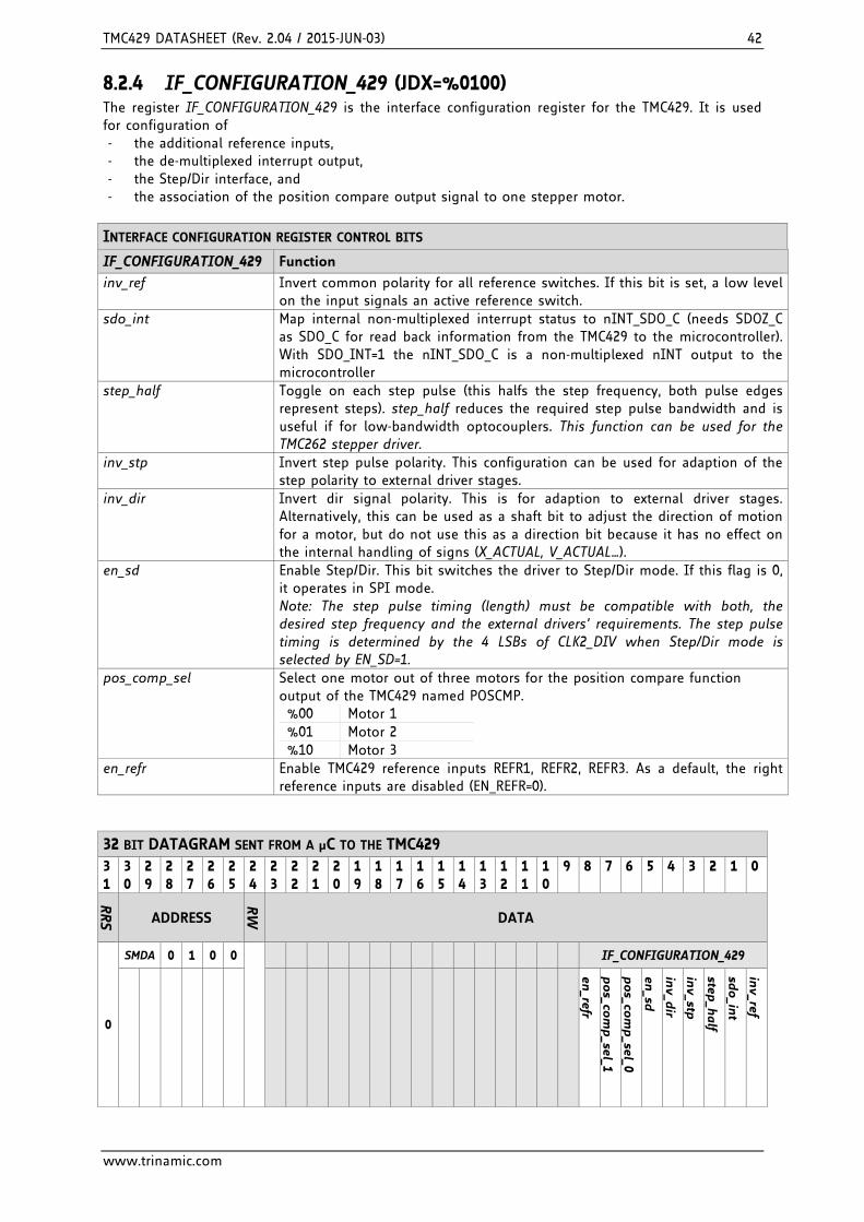
TMC429 DATASHEET (Rev. 2.04 / 2015-JUN-03) 42
www.trinamic.com
8.2.4 IF_CONFIGURATION_429 (JDX=%0100) The register IF_CONFIGURATION_429 is the interface configuration register for the TMC429. It is used for configuration of - the additional reference inputs, - the de-multiplexed interrupt output, - the Step/Dir interface, and - the association of the position compare output signal to one stepper motor.
INTERFACE CONFIGURATION REGISTER CONTROL BITS
IF_CONFIGURATION_429 Function
inv_ref Invert common polarity for all reference switches. If this bit is set, a low level on the input signals an active reference switch.
sdo_int Map internal non-multiplexed interrupt status to nINT_SDO_C (needs SDOZ_C as SDO_C for read back information from the TMC429 to the microcontroller). With SDO_INT=1 the nINT_SDO_C is a non-multiplexed nINT output to the microcontroller
step_half Toggle on each step pulse (this halfs the step frequency, both pulse edges represent steps). step_half reduces the required step pulse bandwidth and is useful if for low-bandwidth optocouplers. This function can be used for the TMC262 stepper driver.
inv_stp Invert step pulse polarity. This configuration can be used for adaption of the step polarity to external driver stages.
inv_dir Invert dir signal polarity. This is for adaption to external driver stages. Alternatively, this can be used as a shaft bit to adjust the direction of motion for a motor, but do not use this as a direction bit because it has no effect on the internal handling of signs (X_ACTUAL, V_ACTUAL…).
en_sd Enable Step/Dir. This bit switches the driver to Step/Dir mode. If this flag is 0, it operates in SPI mode. Note: The step pulse timing (length) must be compatible with both, the desired step frequency and the external drivers’ requirements. The step pulse timing is determined by the 4 LSBs of CLK2_DIV when Step/Dir mode is selected by EN_SD=1.
pos_comp_sel
Select one motor out of three motors for the position compare function output of the TMC429 named POSCMP. %00 Motor 1 %01 Motor 2 %10 Motor 3
en_refr Enable TMC429 reference inputs REFR1, REFR2, REFR3. As a default, the right reference inputs are disabled (EN_REFR=0).
32 BIT DATAGRAM SENT FROM A µC TO THE TMC429 31
30
29
28
27
26
25
24
23
22
21
20
19
18
17
16
15
14
13
12
11
10
9 8 7 6 5 4 3 2 1 0
RRS ADDRESS
RW
DATA
0
SMDA 0 1 0 0
IF_CONFIGURATION_429
en_refr
pos_co
mp_sel_1
pos_co
mp_sel_0
en_sd
inv_d
ir
inv_stp
step_h
alf
sdo_in
t
inv_ref

TMC429 DATASHEET (Rev. 2.04 / 2015-JUN-03) 43
www.trinamic.com
NOTE - After power-on, the TMC429 is in SPI mode. The output signals are logic high until they become
configured for step/direction mode. - Open inputs REFR1, REFR2, and REFR3 in Step/Dir mode have active state if REFMUX=0 due to their
internal pull-up resistors. If EN_REFR=0 these additional reference switch inputs are ignored. - REFMUX does not work in Step/Dir mode because the SPI signal nSCS_S is not available. The
output is signal S2 (step2) in Step/Dir mode - Do not enable unused REFR1, REFR2, REFR3 inputs of the TMC429 as STOP switches if these
inputs are open!
8.2.4.1 POS_COMP_429 (JDX=%0101) POS_COMP_429 defines a position, which becomes compared to the selected motor position (select via pos_comp_sel). Whenever the positions match, the POS_COMP output becomes active.
8.2.4.2 POS_COMP_INT_429 (JDX=%0110) The position compare interrupt mask (M) and interrupt flag (I) register hold the mask and interrupt concerning the position compare function of the TMC429.
8.2.4.3 POWER_DOWN (JDX=%1000) A write to the register address POWER_DOWN sets the TMC429 into the power down mode until it detects a falling edge at the pin nSCS_C. During power down, all internal clocks are stopped. All outputs remain stable, and all register contents are preserved.
8.2.4.4 TYPE_AND_VERSION_429 (JDX=%1001) Read only register that gives type und version of the design. For the TMC429 version 1.01 it reads 0x429101.
8.2.4.5 REFERENCE_SWITCHES l3, r3, l2, r2, l1, and r1 (JDX=%1110) The current state of the reference switches can be read out with this register. The TMC429-LI, TMC429-PI24, and the TMC429-I require different settings of related bits and registers before a read-out of the reference switch bits is possible.
OVERVIEW: REASONABLE SETTINGS FOR DIFFERENT PACKAGES
refmux mot1r en_refr TMC429-I TMC429-PI24 TMC429-LI
1l 1r 2l 2r 3l 3r 1l 1r 2l 2r 3l 3r 1l 1r 2l 2r 3l 3r 0 0 0 x - x - x - x - x - x - x - x - x - 0 0 1 don’t use x x x x x *1 x x x x x x 0 1 0 x x x - - - don’t use don’t use 1 0 0 x x x x x x x x x x x x don’t use
*1 always reads as high level (internal pull-ups)
If it is desired to invert the polarity of the reference switches, the bit inv_ref of the IF_CONFIGURATION_429 register can be set. This allows matching normally open contacts or normally closed contacts.
TMC429-LI To enable right reference switch inputs (REFR1, REFR2 and REFR3) and the associated status bits r1, r2, and r3 for the right switches set en_refr of the register IF_CONFIGURATION_429 to 1 (refer to chapter 0). With the default value en_refr=0 the right reference inputs REFR1, REFR2, and REFR3 are disabled and shown as inactive.
TMC429-PI24 To enable right reference switch inputs (REFR1, REFR2) and the associated status bits r1 and r2 for the right switches set en_refr of the register IF_CONFIGURATION_429 to 1 (refer to chapter 0). With the default value en_refr=0 the right reference inputs REFR1 and REFR2 are disabled and shown as inactive. If a right reference switch for the third motor is needed and SPI motor drivers are used, the refmux bit of the STEPPER MOTOR GLOBAL PARAMETER CONTROL can be set to 1 (refer to chapter 0).
TMC429 DATASHEET (Rev. 2.04 / 2015-JUN-03) 44
www.trinamic.com
Note: the refmux bit is only used for multiplexing reference switch inputs by using a 74HC157 multiplexer. Related to the TMC429-PI24 this is only required for getting a third right reference switch input. The bit continuous_update of the STEPPER MOTOR GLOBAL PARAMETER REGISTER (JDX=%1111) is important for reading out the reference switches if the external multiplexer is used.
TMC429-I With the default value 0 of the bit en_refr (see IF_CONFIGURATION_429, chapter 8.2.4) all three right reference switch inputs of the TMC429-I are inactive, because the inputs are not available on the package. There are different possibilities for configuration and multiplexing of the three reference switch inputs. In chapter 8.2.4.5 they are explained in detail. If all six reference switches are used in an SPI stepper motor driver chain (via an external 74HC157 multiplexer), these inputs are de-multiplexed internally by the TMC429-I. The states of the switches can be read out from the REFERENCE_SWITCHES read-only register. The bit continuous_update of the STEPPER MOTOR GLOBAL PARAMETER REGISTER (JDX=%1111) is important for reading out the reference switches if SPI drivers and the external multiplexer are used.

TMC429 DATASHEET (Rev. 2.04 / 2015-JUN-03) 45
www.trinamic.com
8.2.5 STEPPER MOTOR GLOBAL PARAMETER REGISTER (JDX=%1111) This register holds different configuration bits for the stepper motor driver chain. The absolute address (RRS & ADDRESS) of the stepper motor global parameter register is %01111110 = $7E.
Please note that these registers and bits are mainly for SPI mode. In Step/Dir mode refmux and mot1r can be used for the switch configuration (TMC429-I) and the four LSBs [3…0] of the CLK2_DIV register (named STPDIV_429 in Step/Dir mode) are used for timing. Please refer to chapter 10 for the calculation of Step/Dir timing.
OVERVIEW OF STEPPER MOTOR GLOBAL PARAMETER CONTROL
Register Interface Function
POLARITIES SPI This five bit register defines polarities and chip select signals for the stepper motor driver chain.
cs_ComInd SPI This bit is used to define either if a single chip select signal nSCS_S is used in common for all stepper motor driver chips or if three chip select signals nSCS_S, nSCS2, nSCS3 are used to select stepper motor driver chips individually.
CLK2_DIV SPI and Step/Dir
SPI mode: the eight bits named CLK2_DIV determine the clock frequency of the stepper motor driver chain clock signal SCK_S.
Step/Dir mode: The timing of the Step/Dir interface is controlled by the four LSBs [3…0] of the CLK2_DIV register. The CLK2_DIV[3…0] is named STPDIV_429. Please refer to chapter 10 for the calculation of Step/Dir timing.
LSMD SPI For datagram configuration in SPI mode the number of stepper motor drivers is important. It is represented by the 2 bit parameter LSMD (last stepper motor driver).
continuous_update SPI Setting
This bit can be set if a continuous update of the datagrams to the motor driver chain is necessary and an external multiplexer is used. The continuous update is carried out during periods of rest (velocity=0), too. This bit is required for the automatic current control during rest periods when using SPI drivers.
refmux SPI
refmux is used for multiplexing the reference switch inputs of the TMC429_I (by using a 74HC157 multiplexer). If a right reference switch for the third motor is needed refmux can be used for the TMC429-PI24, too.
mot1r SPI and Step/Dir
This bit is only used with the TMC429-I (16-pin package). Three available reference switches can be adjusted. Refer to chapter 9.1 (including Figure 9.2 and Figure 9.3 for further information).
32 BIT DATAGRAM SENT FROM A µC TO THE TMC429 1 3
0 29
28
27
26
25
24
23
22
21
20
19
18
17
16
15
14
13
12
11
10
9 8 7 6 5 4 3 2 1 0
RRS ADDRESS
RW
DATA
0
1 1 1 1 1 1
CLK2_DIV POLARITIES LSMD
mot1r
refmux
contin
uous_up
date
csCom
monIn
divid
ual
polarity_d
ac_ab
polarity_fd
polarity_p
h_ab
polarity_sck_s
polarity_n
scs_s
last stepper m
oto
r driver

TMC429 DATASHEET (Rev. 2.04 / 2015-JUN-03) 46
www.trinamic.com
8.2.5.1 POLARITIES The global parameter register POLARITIES is only used with SPI motor drivers and defines all polarities necessary.
POLARITIES - GLOBAL PARAMETER REGISTER
POLARITIES (6 bits) Function
polarity_nscs_s Controls the polarity of the selection signal nSCS_S for the stepper motor driver chain. 0 The nSCS_S signal is low active. 1 The nSCS_S signal it is high active.
polarity_sck_s Defines the polarity of the stepper motor driver chain clock signal SCK_S. 0 The clock polarity is according to Figure 11.1. 1 The clock signal SCK_S is inverted.
polarity_ph_ab Defines the polarity of the phase bits for the stepper motor. 0 Normal polarity. 1 Polarity inverted.
polarity_fd Defines the polarity of the fast decay controlling bit. 0 Fast decay is high active. 1 Fast decay is low active.
polarity_dac_ab Defines the polarity of the DAC bit vectors. 0 The DAC bits are high active (normal polarity). 1 The DAC bits are inverted (low active).
8.2.5.2 csCommonIndividual
CSCOMMONINDIVIDUAL - GLOBAL PARAMETER REGISTER csComInd Defines either if a single chip select signal nSCS_S is used in common for
all stepper motor driver chips (e.g. for TMC236, TMC239, TMC246, TMC249) or if three chip select signals nSCS_S, nSCS2, nSCS3 are used to select the stepper motor driver chips individually. This feature is useful only for the TMC429 within the larger packages, where the two additional chip select signals (nSCS2, nSCS3) are available. The common chip select signal nSCS_S is used if csCommonIndividual=0. The polarity control bit for the nSCS_S signal must be set to polarity_nscs_s=0 if csCommonIndividual=1. The chip select polarity is always negative for three individual chips select signals.
8.2.5.3 CLK2_DIV The eight CLK2_DIV bits determine the clock frequency of the motor driver chain in SPI mode. (For information about timing in Step/Dir mode refer to chapter 10.)
UNIT The range of CLK2_DIV is 7, 8, 9, … 253, 254, 255.
- The default value after power-on reset is CLK2_DIV = 15. - A value of 7 (%00000111, $07) is the lower limit for the clock divider parameter. With CLK2_DIV =
7 the clock frequency of SCK_S is at maximum. This value is best for the TRINAMIC drivers TMC236 / TMC239 / TMC246 / TMC249.
- The frequency fSCK_S[Hz] of SCK_S does not become higher for CLK2_DIV < 7, but the signal SCK_S becomes asymmetric with respect to its duty cycle. An asymmetric duty cycle may cause instable SPI transmission to stepper drivers, because the timing might become too fast.
- A value of 255 (%11111111, $FF) is the upper limit for the parameter CLK2_DIV. With CLK2_DIV = 255 the clock frequency of SCK_S is at minimum.
Which level of variations of step frequencies is acceptable depends on the application. At high microstep resolutions the step rate can be a multiple of the SPI rate without impact on the motor smoothness.

TMC429 DATASHEET (Rev. 2.04 / 2015-JUN-03) 47
www.trinamic.com
CLOCK FREQUENCY fSCK_S[Hz]
The frequency fSCK_S[Hz] of the stepper motor driver chain clock signal SCK_S is given by
𝑓𝑓𝑃𝑃𝐶𝐶𝐶𝐶_𝑃𝑃 =𝑓𝑓𝐶𝐶𝐿𝐿𝐶𝐶
2 ∗ (𝐶𝐶𝑃𝑃𝐶𝐶2_𝐷𝐷𝑓𝑓𝐷𝐷 + 1)
- For smooth motion even at high step frequencies the clock frequency fSCK_S[Hz] should be set as high as possible by choosing the parameter CLK2_DIV in consideration of the data clock frequency limit defined by the slowest stepper motor driver chip of the daisy chain.
- If step frequencies reach the order of magnitude of the maximum datagram frequency (determined by the clock frequency of SCK_S and by the datagram length) the step frequencies may jitter, which is an inherent property of SPI communication. Up to which level variations of step frequencies are acceptable depends on the application.
For most applications, a setting of CLK2_DIV = 7 is recommended.
DATAGRAM FREQUENCY fDATAGRAM[Hz]
The datagram frequency fDATAGRAM[Hz] is given by
𝑓𝑓𝐷𝐷𝑅𝑅𝐿𝐿𝑅𝑅𝐷𝐷𝐿𝐿𝑅𝑅𝐿𝐿 =𝑓𝑓𝑃𝑃𝐶𝐶𝐶𝐶_𝑃𝑃[𝑘𝑘𝑘𝑘]
1 + 𝐷𝐷𝐴𝐴𝐷𝐷𝐴𝐴𝐷𝐷𝑅𝑅𝐴𝐴𝑀𝑀_𝑃𝑃𝐿𝐿𝐿𝐿𝐷𝐷𝐷𝐷𝑘𝑘[𝑏𝑏𝑣𝑣𝑡𝑡] + 1
This formula is an approximation for the upper limit. - For CLK2_DIV = 7 the processing of the NxM bit (next motor bit) requires 1 SPI clock cycle. - The processing of the NxM bit requires 1.5 SPI clock cycles for CLK2_DIV > 7.
As result for a chain of three drivers with 12 bit datagram length each, the upper limit of the datagram frequency is
𝑓𝑓𝐷𝐷𝑅𝑅𝐿𝐿𝑅𝑅𝐷𝐷𝐿𝐿𝑅𝑅𝐿𝐿[Hz] =𝑓𝑓𝑃𝑃𝐶𝐶K_S[𝑘𝑘𝑘𝑘]
1 + 3 ∗ (12 + 1) + 1=𝑓𝑓𝑃𝑃𝐶𝐶K_S[𝑘𝑘𝑘𝑘]
41
8.2.5.4 LSMD - Last Stepper Motor Driver For the datagram configuration in SPI mode the number of stepper motor drivers is important. It is represented by the parameter LSMD (last stepper motor driver).
SETTING THE NUMBER OF STEPPER MOTOR DRIVERS LSMD Number motor drivers
%00 (=0) 1 motor driver %01 (=1) 2 motor drivers %10 (=2) 3 motors drivers %11 (=3) not allowed!
TMC429 DATASHEET (Rev. 2.04 / 2015-JUN-03) 48
www.trinamic.com
8.2.5.5 continuous_update The TMC429 in SPI mode sends datagrams to the stepper motor driver chain only on demand. The continuous_update bit offers two possibilities.
CONTINUOUS_UPDATE SETTINGS
continuous _update Description
0
No datagrams are sent during rest periods if continuous_update is set to 0. This reduces communication traffic. The multiplexed reference switch inputs are only processed while datagrams are sent to the stepper motor driver chain. A stepper motor (stopped at reference switch / switch became inactive) stays at rest until a new datagram is sent from the TMC429 to the stepper motor driver chain. Afterwards, the stepper motor can be either moved into the direction opposite to the reference switch or it can be moved in both directions by disabling the automatic stop function. There is no automatic coil current scaling if the motors are at rest! This setting is recommended for low power applications, e.g. if the stepper motor drivers shall be put into standby mode.
1
When using a reference switch multiplexer, with the reference switches configured to stop associated stepper motors automatically, the configuration bit continuous_update must be set to 1. This forces the periodic sending of datagrams to the stepper motor driver chain and samples the reference switches periodically, if all stepper motors are at rest. With this, a stepper motor restarts if the associated reference switch becomes inactive. For automatic coil current scaling this bit must be set to 1. The coil current is scaled even though all motors are at rest (velocity=0). Refer to chapter 8.1.9. This is the normal setting enabling all features.
The continuous update datagram frequency is given by
𝑓𝑓𝑟𝑟𝑟𝑟𝑐𝑐𝑟𝑟_𝑢𝑢[Hz] =𝑓𝑓𝐶𝐶𝐿𝐿𝐶𝐶[Hz] ∗ ( 1
2RAMP_DIV_0 + 12RAMP_DIV_1 + 1
2RAMP_DIV_2)
32768
where RAMP_DIV_0, RAMP_DIV_1, and RAMP_DIV_2 are the RAMP_DIV settings of the three stepper motors.

TMC429 DATASHEET (Rev. 2.04 / 2015-JUN-03) 49
www.trinamic.com
9 Reference Switch Inputs
9.1 Reference Switch Configuration, mot1r, and refmux mot1r is useful for single or dual motor applications with the TMC429-I. It can be used in SPI mode and in Step/Dir mode. In a configuration with SPI drivers and external reference multiplexer (refmux =1) all reference switches are available even with TMC429-I. This configuration may also be useful with the TMC429-PI24. Without multiplexing the TMC429-PI24 offers three left switches but only two right switches.
ASSOCIATION OF REFERENCE INPUTS DEPENDING ON CONFIGURATION BITS
refmux TMC429-I and TMC429-PI24
SPI only
mot1r SPI only
Motor 1 Motor 2 Motor 3
left switch right switch left switch right switch left switch right switch
0 0 REF1 % REF2 % REF3 %
0 1 REF1 REF3 REF2 % % %
1 0 REF1_LEFT REF1_RIGHT REF2_LEFT REF2_RIGHT REF3_LEFT REF3_RIGHT
1 1 REF1_LEFT REF1_RIGHT REF2_LEFT REF2_RIGHT REF3_LEFT REF3_RIGHT
NOTES - With refmux set to 0, the association of the reference switch inputs REF1, REF2, and REF3 depend
on the setting of mot1r. - If reference switch multiplexing is enabled, mot1r is ignored. - Power-on default values are refmux=0 and mot1r=0. - After power-on-reset, the default setting (refmux=0 and mot1r=0) selects the basic single reference
switch configuration as outlined in Figure 9.2.
TMC429-LI AND TMC429-PI24 The TMC429-LI offers two reference switches (right and left) for each stepper motor. Therefore the TMC429-LI does not need to be configured with refmux and mot1r. The TMC429-PI24 offers one left reference switch for each motor and a right reference switch for motor 1 and motor 2. refmux may be used with the TMC429-PI24 in SPI mode if a right reference switch for motor 3 is needed. mot1r has no relevance for the TMC429-PI24.
SCK_S
SDO_S
SDI_S
nSCS_S
REF2R REF3REF1R
TEST GNDCLK V5V33
SCK_C
SDI_C
nSCS_C
SDOZ_C
nINT_SDO_C
REF1 REF3RREF2
SCK_S
SDO_S
SDI_S
nSCS_S
REF2R REF3REF1R
TEST GNDCLK V5V33
SCK_C
SDI_C
nSCS_C
SDOZ_C
nINT_SDO_C
REF1 REF2
TMC429-LI TMC429-PI24
Figure 9.1 TMC429-LI has three right reference inputs. TMC429-PI24 has two right reference inputs.

TMC429 DATASHEET (Rev. 2.04 / 2015-JUN-03) 50
www.trinamic.com
TMC429-I The TMC429-I offers three reference switch inputs, which can be used left-side-only or two-one-zero as shown in Figure 9.2 and in Figure 9.3. mot1r is used to set the reference switch configuration (left-side-only resp. two-one-zero). refmux is used for the configuration of multiplexing the three reference switches (e.g. with 74HC157 multiplexer).
LEFT-SIDE-ONLY
The power-on default value of mot1r is 0. With this default value, REF1 is associated to the left reference switch of stepper motor #1, REF2 is associated to the left reference switch of stepper motor #2, and REF3 is associated to the left reference switch of stepper motor #3.
REF
_SW
3_LE
FT
REF
_SW
2_LE
FT
REF
_SW
1_LE
FT
SCK_S
SDO_S
SDI_S
nSCS_SREF2 REF3REF1
TEST GND
SDI_C
nSCS_C
SCK_C
SDO_C CLK V5V33
TMC429-I
+VCC+VCC+VCC
Figure 9.2 Reference switch configuration left-side-only for mot1r=0 (and refmux=0)
TWO-ONE-ZERO
If mot1r is set to 1 the input REF1 is also associated with the left reference switch of stepper motor #1. REF2 is also associated to the left reference switch of stepper motor #2. But, the input REF3 is associated to the right reference switch of stepper motor #1 and no reference switch input is associated to stepper motor number#3 (see Figure 9.3)
+VCC +VCC+VCC
No reference switch for stepper motor 3.
SCK_S
SDO_S
SDI_S
nSCS_SREF2 REF3REF1
TEST GND
SDI_C
nSCS_C
SCK_C
SDO_C CLK V5V33
TMC429-I
REF
_SW
2_LE
FT
REF
_SW
1_RI
GHT
REF
_SW
1_LE
FT
Figure 9.3 Reference switch configuration two-one-zero for mot1r=1 (and refmux=0)
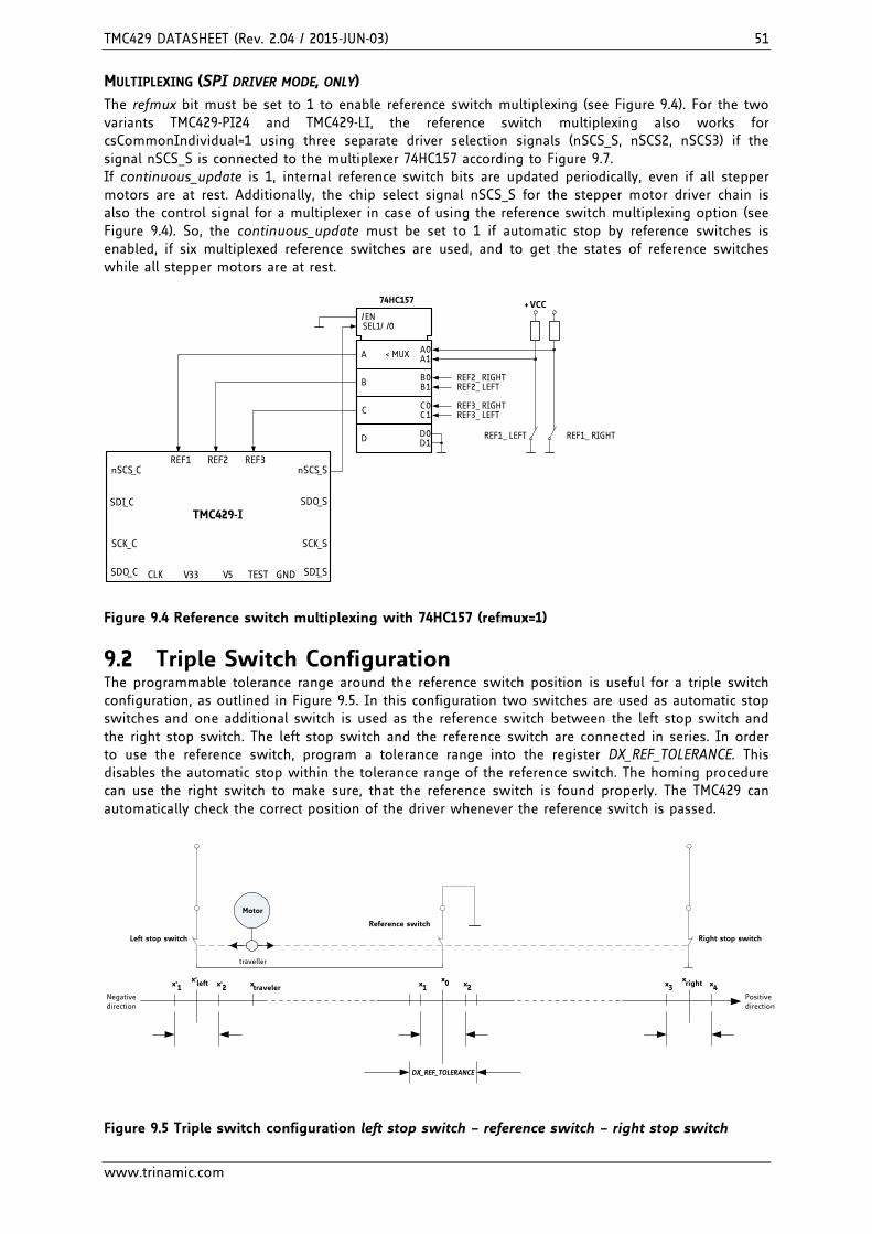
TMC429 DATASHEET (Rev. 2.04 / 2015-JUN-03) 51
www.trinamic.com
MULTIPLEXING (SPI DRIVER MODE, ONLY) The refmux bit must be set to 1 to enable reference switch multiplexing (see Figure 9.4). For the two variants TMC429-PI24 and TMC429-LI, the reference switch multiplexing also works for csCommonIndividual=1 using three separate driver selection signals (nSCS_S, nSCS2, nSCS3) if the signal nSCS_S is connected to the multiplexer 74HC157 according to Figure 9.7. If continuous_update is 1, internal reference switch bits are updated periodically, even if all stepper motors are at rest. Additionally, the chip select signal nSCS_S for the stepper motor driver chain is also the control signal for a multiplexer in case of using the reference switch multiplexing option (see Figure 9.4). So, the continuous_update must be set to 1 if automatic stop by reference switches is enabled, if six multiplexed reference switches are used, and to get the states of reference switches while all stepper motors are at rest.
A1A0A < MUX
B
C
D
B1B0
C1C0
D1D0
SEL1/ /0/EN
REF1_ LEFT REF1_ RIGHT
REF2_ LEFTREF2_ RIGHT
REF3_ LEFTREF3_ RIGHT
+ VCC74HC157
SCK_S
SDO_S
SDI_S
nSCS_SREF2 REF3REF1
TEST GND
SDI_C
nSCS_C
SCK_C
SDO_C CLK V5V33
TMC429-I
Figure 9.4 Reference switch multiplexing with 74HC157 (refmux=1)
9.2 Triple Switch Configuration The programmable tolerance range around the reference switch position is useful for a triple switch configuration, as outlined in Figure 9.5. In this configuration two switches are used as automatic stop switches and one additional switch is used as the reference switch between the left stop switch and the right stop switch. The left stop switch and the reference switch are connected in series. In order to use the reference switch, program a tolerance range into the register DX_REF_TOLERANCE. This disables the automatic stop within the tolerance range of the reference switch. The homing procedure can use the right switch to make sure, that the reference switch is found properly. The TMC429 can automatically check the correct position of the driver whenever the reference switch is passed.
Negative direction
x'1 x'2
Left stop switch
x'left x1 x2
Reference switch
x0
Positive direction
x3 x4xright
Right stop switch
DX_REF_TOLERANCE
Motor
traveller
xtraveler
Figure 9.5 Triple switch configuration left stop switch – reference switch – right stop switch

TMC429 DATASHEET (Rev. 2.04 / 2015-JUN-03) 52
www.trinamic.com
9.3 Homing Procedure In order to home the drive, the reference switch position xref must be determined after each power on (see Figure 9.6).
PROCEED AS FOLLOWS: 1. Due to mechanical inaccuracy of switches, the reference switch is active within the following
range: x1 < xref < x2, where x1 and x2 may vary. If the traveler is within the range x1 < xtraveler < x2 at the start of the homing procedure, it is necessary to leave this range, because the associated reference switch is active. A dummy write access to X_LATCHED initializes the position latch register.
2. With the traveler within the range x2 < xtraveler < xmax and the register X_LATCHED initialized, the position x2 can simply be determined by motion with a target position X_TARGET set to –xmax.
3. When reaching position x2 the position is latched automatically. 4. With stop switch enabled, the stepper motor automatically stops if the position x2 is reached. 5. Now, set the DX_REF_TOLERANCE in order to allow motion within the active reference switch
range x1 < xref < x2 and to move the traveler to a position xtraveler < x1 if desired. 6. Afterwards initialize the register X_LATCHED again to latch the position x1 by a motion to a
target position xtraveler < x1. 7. When the positions x1 and x2 are determined the reference position xref = (x1 + x2 ) / 2 can be set.
Finally, one should move to the target position X_TARGET = xref and set X_TARGET := 0 and X_ACTUAL := 0 when reached.
mechanical inaccuracy of switches(switching hysteresis)
x1 x2
reference
switch
dx2dx1
DX_REF_TOLERANCE
xref xmax
Motor
traveller
xtraveler
Negative direction
Positive direction
Figure 9.6 Reference search
9.4 Simultaneous Start of up to Three Stepper Motors Starting stepper motors simultaneously can be achieved by sending successive datagrams starting the stepper motors. If the delay between those datagrams is of the magnitude of some microseconds, the stepper motors can be considered as started simultaneously. Feeding the reference switch signals through or gates (see Figure 9.7) allows exact simultaneous start of the stepper motors under software control.
A1A0A < MUX
B
C
D
B1B0
C1C0
D1D0
SEL1/ /0/EN
REF1_LEFT REF1_RIGHT
REF2_LEFTREF2_RIGHT
REF3_LEFTREF3_RIGHT
+VCC
74HC157
74HC32
hold
hold
SCK_S
SDO_S
SDI_S
nSCS_SREF2 REF3REF1
TEST GND
SDI_C
nSCS_C
SCK_C
SDO_C CLK V5V33
TMC429-I
SCK_S
SDO_S
SDI_S
nSCS_S
REF2R REF3REF1R
TEST GNDCLK V5V33
SCK_C
SDI_C
nSCS_C
SDOZ_C
nINT_SDO_C
REF1 REF3RREF2
TMC429-LI
Figure 9.7 Reference switch gateing for exact simultanous stepper motor start
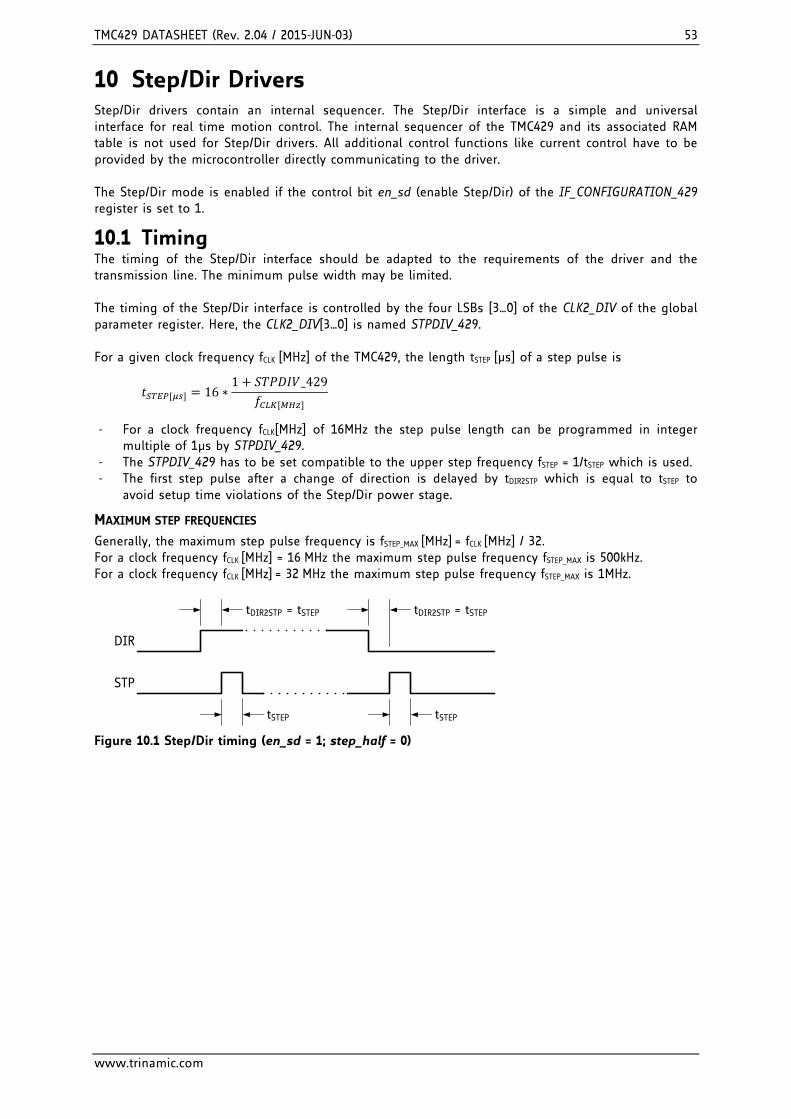
TMC429 DATASHEET (Rev. 2.04 / 2015-JUN-03) 53
www.trinamic.com
10 Step/Dir Drivers Step/Dir drivers contain an internal sequencer. The Step/Dir interface is a simple and universal interface for real time motion control. The internal sequencer of the TMC429 and its associated RAM table is not used for Step/Dir drivers. All additional control functions like current control have to be provided by the microcontroller directly communicating to the driver. The Step/Dir mode is enabled if the control bit en_sd (enable Step/Dir) of the IF_CONFIGURATION_429 register is set to 1.
10.1 Timing The timing of the Step/Dir interface should be adapted to the requirements of the driver and the transmission line. The minimum pulse width may be limited. The timing of the Step/Dir interface is controlled by the four LSBs [3…0] of the CLK2_DIV of the global parameter register. Here, the CLK2_DIV[3…0] is named STPDIV_429. For a given clock frequency fCLK [MHz] of the TMC429, the length tSTEP [µs] of a step pulse is
𝑡𝑡𝑃𝑃𝐿𝐿𝐿𝐿𝑅𝑅[𝜇𝜇𝑢𝑢] = 16 ∗1 + 𝑓𝑓𝐷𝐷𝑓𝑓𝐷𝐷𝑓𝑓𝐷𝐷_429
𝑓𝑓𝐶𝐶𝐿𝐿𝐶𝐶[𝐿𝐿𝐻𝐻𝐻𝐻]
- For a clock frequency fCLK[MHz] of 16MHz the step pulse length can be programmed in integer multiple of 1µs by STPDIV_429.
- The STPDIV_429 has to be set compatible to the upper step frequency fSTEP = 1/tSTEP which is used. - The first step pulse after a change of direction is delayed by tDIR2STP which is equal to tSTEP to
avoid setup time violations of the Step/Dir power stage.
MAXIMUM STEP FREQUENCIES Generally, the maximum step pulse frequency is fSTEP_MAX [MHz] = fCLK [MHz] / 32. For a clock frequency fCLK [MHz] = 16 MHz the maximum step pulse frequency fSTEP_MAX is 500kHz. For a clock frequency fCLK [MHz] = 32 MHz the maximum step pulse frequency fSTEP_MAX is 1MHz.
STP
DIR
tSTEP
tDIR2STP = tSTEP
tSTEP
tDIR2STP = tSTEP
Figure 10.1 Step/Dir timing (en_sd = 1; step_half = 0)

TMC429 DATASHEET (Rev. 2.04 / 2015-JUN-03) 54
www.trinamic.com
11 SPI Mode Driver Interface The TMC429 contains a microstep sequencer, which directly connects to SPI stepper motor drivers. The internal sequencer provides the full set of control signals for three stepper motor driver ICs. The SPI datagram is individually configurable for each stepper motor driver chip of the daisy chain. This is necessary, because there is no standard for the sequence, the meaning, and the number of the control bits for serial stepper motor drivers. The stepper motor driver datagram configuration adapts the specific sequence of control bits required by the driver IC. It is stored within the first 32 addresses representing 64 values of the on-chip RAM (see chapter 10). The TMC429 is simply configurable by sending a fixed sequence of datagrams to initialize it after power-up. Once initialized, the TMC429 autonomously generates the datagrams for the stepper motor driver daisy chain without any additional interventions of the microcontroller. To operate the TMC429 in SPI mode set en_sd to 0 (see chapter 0). The addressing of the stepper motor drivers within a daisy chain is determined by their position in the SPI chain: the last IC in the chain is motor driver 0.
For TRINAMIC drivers, configuration data is provided.
11.1 Bus Signals Signal Description TMC429 Stepper Driver
Bus clock input SCK_S Serial data input SDI_S Serial data output SDO_S Chip select input nSCS_S
11.2 Timing The timing of the serial stepper motor interface is similar to that of the microcontroller interface.
CLK
tCLK
SCK_S
nSCS_S
SDI_S
SDO_S
sdi_s_bit#0
tPD tPD tPD
1 x sampled SDI_S
tSUSCSdrv tHDSCSdrv tCKSL tCKSH
sdo_s_bit#0
sdi_s_bit#n-1
sdo_s_bit#n-1sdo_s_bit#1
sdi_s_bit#1
sdo_s_bit#n
sdi_s_bit#n
m datagram bits
one full stepper motor driver datagram
tDATAGRAMdrv
1 x sampled SDI_Sm x sampled SDI_S
Figure 11.1 Timing diagram of the serial stepper motor driver interface
EXPLANATORY NOTES - The clock divider provides 16 up to 512 clock cycles (tCLK) for a serial driver interface data clock
period. - The default duration of a clock period (tSCKCL+tSCKCH) of the signal nSCS_S is 16+16=32 clock
periods of the clock signal CLK. - The minimal duration of a serial interface clock period (tSCKCL+tSCKCH) is 8+8=16 clock cycles of
signal CLK. Set CLK_DIV=7. This setting provides best performance in most cases. - The polarities of the signals nSCS_S and SCK_S are programmable to use driver chips with
inverted polarities without additional glue logic. - The input SDI_S of the serial driver interface must always be driven to a defined level. To avoid
high impedance (Z) at this input pin while the stepper motor driver chain is idle, a pull-up resistor or a pull-down resistor of 10 KΩ is required at the input.

TMC429 DATASHEET (Rev. 2.04 / 2015-JUN-03) 55
www.trinamic.com
TIMING CHARACTERISTICS OF SERIAL STEPPER MOTOR DRIVER INTERFACE Symbol Parameter Min Typ Max Unit
tSUSCSdrv 8 16 256 CLK periods
tHDSCSdrv 8 16 256 CLK periods
tCKSL 8 16 256 CLK periods
tCKSH 8 16 256 CLK periods
tDAMAGRAMdrv Datagram Length 8+8+1*16+8+8=48 512+64*512+512= 33792
CLK periods
tDAMAGRAMdrv Datagram Duration for 1 - 64 bits @ fCLK = 16 MHz
3 2112 µs
tDAMAGRAMdrv Datagram Duration for 1 – 64 bits @ fCLK = 32 MHz
3 1056 µs
tPD CLK-rising-edge to Outputs Delay
5 ns
11.3 RAM Address Partitioning and Data Organization The SPI datagram for each stepper motor driver is composed of internal sequencer output signals provided by the microstep unit of the TMC429 individually for each stepper motor. Each internal sequencer output signal is represented by a five bit code word called driver configuration code. The order of internal sequencer output signals forming the SPI datagrams for the stepper motor driver daisy chain is defined by the order of driver configuration code words in the configuration RAM area.
The on-chip RAM capacity is 128 x 6 bit. The 128 on-chip RAM cells of 6 bit width are addressed via 64 addresses with 2 x 6 data words. From the addressing point of view, the address space enfolds 64 addresses of 12 bit wide data. The 64 addresses are partitioned into two ranges of 32 addresses – selected by the register RAM select RRS bit.
The registers of the TMC429 are addressed with RRS=0. The on-chip RAM is addressed with RRS=1.
PARTITIONING OF THE ON-CHIP RAM ADDRESS SPACE
32 BIT DATAGRAM SENT FROM A µC TO THE TMC429 VIA PIN SDI_C 31
30
29
28
27
26
25
24
23
22
21
20
19
18
17
16
15
14
13
12
11
10
9 8 7 6 5 4 3 2 1 0
RRS ADDRESS
RW
DATA
data @ odd RAM
addresses
data @ even RAM addresses
1 0
32 x (2x6 bit)
driver chain datagram
configuration range
NxM
_1
signal_codes
NxM
_0
signal_codes
1 1
32 x (2x6 bit)
quarter period sine wave LUT
range
quarter sine wave
values (amplitude)
quarter sine wave
values (amplitude)
DRIVER CHAIN DATA CONFIGURATION The sequencer internally generates a number of control signals available for transmission to SPI driver ICs. These sequencer output signals are selected as configured by the internal stepper motor driver datagram configuration table. The first 32 addresses are provided for the configuration of the serial stepper motor driver chain. Each of these 32 addresses stores two configuration words, composed of the so called NxM (next motor) bit together with the 5 bit wide driver configuration code. While sending a datagram, the driver
TMC429 DATASHEET (Rev. 2.04 / 2015-JUN-03) 56
www.trinamic.com
configuration code words are read sequentially beginning with the first address of the driver chain datagram configuration memory range. Each driver configuration code word selects a signal provided by the microstep unit.
MICROSTEP TABLE The second 32 addresses are provided to store the microstep table. This table usually is a quarter period of a sine wave or of a periodic function, which has been optimized for a given motor type. Different stepper motors may step with different microstep resolutions, but the microstep look up table (LUT) is the same for all stepper motors controlled by one TMC429. Any quarter wave period stored in the microstep table is expanded automatically to a full period wave together with its 90° phase shifted wave.
NXM The NxM bit tells the TMC429 that the last bit of a motor driver SPI register is reached. The TMC429 increments the internal stepper motor addressing counter and switches to the next driver in the chain after reading an SPI configuration word with NxM=1. If the internal stepper motor addressing counter is equivalent to the last stepper motor driver LSMD parameter, the datagram transmission is finished and the counter is preset to %00 for the next datagram transmission to the stepper motor driver chain.
The total data word width is six bit: five for an internal sequencer output signals and one NxM bit.
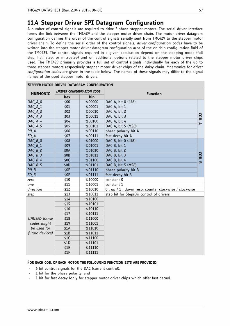
TMC429 DATASHEET (Rev. 2.04 / 2015-JUN-03) 57
www.trinamic.com
11.4 Stepper Driver SPI Datagram Configuration A number of control signals are required to drive 2-phase stepper motors. The serial driver interface forms the link between the TMC429 and the stepper motor driver chain. The motor driver datagram configuration defines the order of the control signals serially sent from TMC429 to the stepper motor driver chain. To define the serial order of the control signals, driver configuration codes have to be written into the stepper motor driver datagram configuration area of the on-chip configuration RAM of the TMC429. The control signals required in a given application depend on the stepping mode (full step, half step, or microstep) and on additional options related to the stepper motor driver chips used. The TMC429 primarily provides a full set of control signals individually for each of the up to three stepper motors respectively stepper motor driver chips of the daisy chain. Mnemonics for driver configuration codes are given in the table below. The names of these signals may differ to the signal names of the used stepper motor drivers.
STEPPER MOTOR DRIVER DATAGRAM CONFIGURATION
MNEMONIC DRIVER CONFIGURATION CODE
Function hex bin
DAC_A_0 $00 %00000 DAC A, bit 0 (LSB)
COIL A
DAC_A_1 $01 %00001 DAC A, bit 1 DAC_A_2 $02 %00010 DAC A, bit 2 DAC_A_3 $03 %00011 DAC A, bit 3 DAC_A_4 $04 %00100 DAC A, bit 4 DAC_A_5 $05 %00101 DAC A, bit 5 (MSB) PH_A $06 %00110 phase polarity bit A FD_A $07 %00111 fast decay bit A DAC_B_0 $08 %01000 DAC B, bit 0 (LSB)
COIL B
DAC_B_1 $09 %01001 DAC B, bit 1 DAC_B_2 $0A %01010 DAC B, bit 2 DAC_B_3 $0B %01011 DAC B, bit 3 DAC_B_4 $0C %01100 DAC B, bit 4 DAC_B_5 $0D %01101 DAC B, bit 5 (MSB) PH_B $0E %01110 phase polarity bit B FD_B $0F %01111 fast decay bit B zero $10 %10000 constant 0 one $11 %10001 constant 1 direction $12 %10010 0 : up / 1 : down resp. counter clockwise / clockwise step $13 %10011 step bit for Step/Dir control of drivers
UNUSED (these codes might be used for
future devices)
$14 %10100
$15 %10101 $16 %10110 $17 %10111 $18 %11000 $19 %11001 $1A %11010 $1B %11011 $1C %11100 $1D %11101 $1E %11110 $1F %11111
FOR EACH COIL OF EACH MOTOR THE FOLLOWING FUNCTION BITS ARE PROVIDED: - 6 bit control signals for the DAC (current control), - 1 bit for the phase polarity, and - 1 bit for fast decay (only for stepper motor driver chips which offer fast decay).

TMC429 DATASHEET (Rev. 2.04 / 2015-JUN-03) 58
www.trinamic.com
FOR BOTH COILS OF EACH MOTOR FURTHER FUNCTION BITS ARE PROVIDED: - 1 constant configuration bit named zero, - 1 constant configuration bit named one, - 1 direction bit for Step/dir control of drivers, and - 1 step bit for Step/Dir control of drivers. Figure 11.2 outlines how to connect the control signals of the TMC429 with the signals used to control the digital part of a stepper motor driver.
Serial Driver Interface
ZeroOne
DAC_A_0DAC_A_1
...
PH_AFD_A
DAC_B_0DAC_B_1
...
PH_BFD_B
DirectionStep
3 x
Micro Stepping Unit(incl. sequencer)
TMC429Multiple
Ported RAM
Serial-to-Parallel Interface(s)
CA3
PHA
MDA
Stepper Motor DriverControl Logic
Stepper Motor Driver (Chain)e.g. TMC236 / TMC239 / TMC246 / TMC249
MSB
LSB
CA2CA1CA0
CB3
PHB
MDB
CB2CB1CB0
Status Signals DAC_A_5
PH_A
FD_A
DAC_A_4DAC_A_3DAC_A_2
DAC_B_5
PH_B
FD_B
DAC_B_4DAC_B_3DAC_B2
CA3
PHA
MDA
CA2CA1CA0
CB3
PHB
MDB
CB2CB1CB0
n
Status Signals
Control Signals
Status Signals n
Figure 11.2 Serially transmitted control and status signals between TMC429 and driver chain
If fullstep operation of an SPI stepper motor is desired, e.g. at higher velocities, the driver configuration codes for the DAC bits can be replaced by constant ‘1’ bits (signal code %11) on the fly during high velocity motion. This way, the microstep resolution does not need to be changed. UNDERSTANDING THE CONFIGURABLE SPI DATAGRAM SEQUENCER
1. The TMC429 sends datagrams to the stepper motor driver chain only on demand. To guarantee the integrity of each datagram, the status of all internal sequencer output signals is buffered internally before sending.
2. Afterwards, the transmission starts with selection of the buffered internal sequencer output signals of the first motor (SMDA=%00) by reading the first driver configuration code word (even data word at on-chip RAM address %00000) from on-chip configuration RAM area.
3. The driver configuration codes select the sequencer output signals provided for the first stepper motor. The first stepper motor is addressed until the NxM (next motor) bit is read from on-chip configuration RAM. The stepper motor driver address is incremented with each NxM=1 as long as the current stepper motor driver address is below the value set by the parameter LSMD (last stepper motor driver). If the stepper motor driver address is equivalent to the LSMD parameter, NxM=1 indicates the completion of the transmission.
4. Now, the stepper motor driver address counter of the serial interface is reinitialized to %00 and the unit waits for the next transmission request.
Note - The order of driver configuration codes in the on-chip RAM configuration area determines the
order of datagram bits for the stepper motor driver chain, whereas the prefixed NxM bit determines the stepper motor driver positions. If no NxM bit with a value of 1 is stored within the on-chip RAM, the TMC429 will send endlessly.
- The on-chip RAM has to be configured first! - After power-on reset, the registers of the TMC429 are initialized in a way that no transmission of
datagrams to the motor driver chain is required. - Access to on-chip RAM is always possible, also during transmission of datagrams to the driver
chain.

TMC429 DATASHEET (Rev. 2.04 / 2015-JUN-03) 59
www.trinamic.com
11.4.1 Initialization of On-Chip RAM by µC after Power-On After the automatic power-on reset all registers are initialized and all stepper motors are at rest. The on-chip RAM of the TMC429 is initialized with a default configuration for a TMC23x or TM24x stepper motor driver chain. Writing to TMC429 registers may cause action of the stepper motor units (initiated by the TMC429) which results in sending datagrams to the stepper motor driver chain! Before moving a motor using other stepper motor drivers than TMC236/TMC239/TMC246/TMC249 in an SPI chain the on-chip RAM must be initialized.
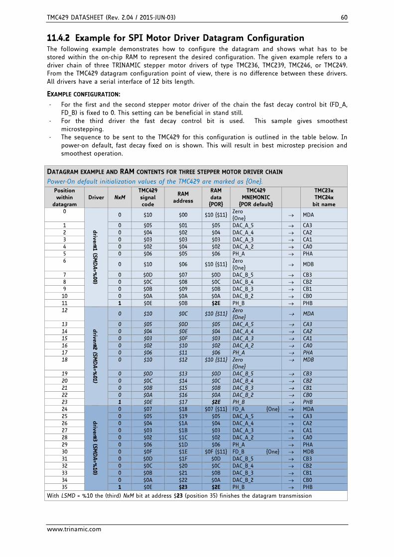
TMC429 DATASHEET (Rev. 2.04 / 2015-JUN-03) 60
www.trinamic.com
11.4.2 Example for SPI Motor Driver Datagram Configuration The following example demonstrates how to configure the datagram and shows what has to be stored within the on-chip RAM to represent the desired configuration. The given example refers to a driver chain of three TRINAMIC stepper motor drivers of type TMC236, TMC239, TMC246, or TMC249. From the TMC429 datagram configuration point of view, there is no difference between these drivers. All drivers have a serial interface of 12 bits length.
EXAMPLE CONFIGURATION: - For the first and the second stepper motor driver of the chain the fast decay control bit (FD_A,
FD_B) is fixed to 0. This setting can be beneficial in stand still. - For the third driver the fast decay control bit is used. This sample gives smoothest
microstepping. - The sequence to be sent to the TMC429 for this configuration is outlined in the table below. In
power-on default, fast decay fixed on is shown. This will result in best microstep precision and smoothest operation.
DATAGRAM EXAMPLE AND RAM CONTENTS FOR THREE STEPPER MOTOR DRIVER CHAIN Power-On default initialization values of the TMC429 are marked as One.
Position within
datagram Driver NxM
TMC429 signal code
RAM address
RAM data POR
TMC429 MNEMONIC
POR default
TMC23x TMC24x
bit name 0
driver#1 (SM
DA=%
00)
0 $10 $00 $10 $11 Zero One
→ MDA
1 0 $05 $01 $05 DAC_A_5 → CA3 2 0 $04 $02 $04 DAC_A_4 → CA2 3 0 $03 $03 $03 DAC_A_3 → CA1 4 0 $02 $04 $02 DAC_A_2 → CA0 5 0 $06 $05 $06 PH_A → PHA 6
0 $10 $06 $10 $11 Zero One
→ MDB
7 0 $0D $07 $0D DAC_B_5 → CB3 8 0 $0C $08 $0C DAC_B_4 → CB2 9 0 $0B $09 $0B DAC_B_3 → CB1 10 0 $0A $0A $0A DAC_B_2 → CB0 11 1 $0E $0B $2E PH_B → PHB 12
driver#2 (SM
DA=%
01)
0 $10 $0C $10 $11 Zero One
→ MDA
13 0 $05 $0D $05 DAC_A_5 → CA3 14 0 $04 $0E $04 DAC_A_4 → CA2 15 0 $03 $0F $03 DAC_A_3 → CA1 16 0 $02 $10 $02 DAC_A_2 → CA0 17 0 $06 $11 $06 PH_A → PHA 18 0 $10 $12 $10 $11 Zero
One → MDB
19 0 $0D $13 $0D DAC_B_5 → CB3 20 0 $0C $14 $0C DAC_B_4 → CB2 21 0 $0B $15 $0B DAC_B_3 → CB1 22 0 $0A $16 $0A DAC_B_2 → CB0 23 1 $0E $17 $2E PH_B → PHB 24
driver#3 (SM
DA=%
10)
0 $07 $18 $07 $11 FD_A One → MDA 25 0 $05 $19 $05 DAC_A_5 → CA3 26 0 $04 $1A $04 DAC_A_4 → CA2 27 0 $03 $1B $03 DAC_A_3 → CA1 28 0 $02 $1C $02 DAC_A_2 → CA0 29 0 $06 $1D $06 PH_A → PHA 30 0 $0F $1E $0F $11 FD_B One → MDB 31 0 $0D $1F $0D DAC_B_5 → CB3 32 0 $0C $20 $0C DAC_B_4 → CB2 33 0 $0B $21 $0B DAC_B_3 → CB1 34 0 $0A $22 $0A DAC_B_2 → CB0 35 1 $0E $23 $2E PH_B → PHB
With LSMD = %10 the (third) NxM bit at address $23 (position 35) finishes the datagram transmission

TMC429 DATASHEET (Rev. 2.04 / 2015-JUN-03) 61
www.trinamic.com
The stepper motor driver datagram configuration can be accessed at any time without conflict, e.g. to change between a configuration using fast decay versus a configuration where fast decay is disabled.
CONFIGURATION DATAGRAM SEQUENCE FOR THE EXAMPLE with – = don’t cares
binary datagram specification : hexadecimal datagram %10000000----------000101–010000 : $80000510 %10000010----------000011–000100 : $82000304 %10000100----------000110–000010 : $84000602 %10000110----------001101–010000 : $86000D10 %10001000----------001011–001100 : $88000B0C %10001010----------101110–001010 : $8a002E0A %10001100----------000101–010000 : $8c000510 %10001110----------000011–000100 : $8e000304 %10010000----------000110–000010 : $90000602 %10010010----------001101–010000 : $92000D10 %10010100----------001011–001100 : $94000B0C %10010110----------101110–001010 : $96002E0A %10011000----------000101–000111 : $98000507 %10011010----------000011–000100 : $9a000304 %10011100----------000110–000010 : $9c000602 %10011110----------001101–001111 : $9e000D0F %10100000----------001011–001100 : $a0000B0C %10100010----------101110–001010 : $a2002E0A
11.4.3 Initialization of SPI Motor Drivers Using Cover Datagrams Some stepper drivers require an initialization. When they are driven in SPI-Mode by a TMC429 there is no direct access from the µC to stepper motor drivers. The TMC429 supports tunneling of data from the µC to each stepper motor driver in the chain. This mechanism is called cover datagram. Also, status information from the drivers may need to be fed back to the µC for special functions. This is enabled by a set of two registers: datagram-low-word and datagram-high-word buffer data sent back from the drivers.
PROCEDURE: - The TMC429 enables direct communication between the microcontroller and the stepper motor
driver chain by sending a cover datagram. - The position cover_position and actual length cover_len of a cover datagram is specified by
writing them into a common register. - Writing an up to 24 bit wide cover datagram to the register cover_datagram will fade in that
cover datagram into the next datagram sent to the stepper motor driver chain.

TMC429 DATASHEET (Rev. 2.04 / 2015-JUN-03) 62
www.trinamic.com
11.5 Initialization of Microstep Look-Up Table For an SPI driver chain the TMC429 provides a look-up table (LUT) of 64 values of 6 bit for microstepping. The microstep LUT can be adapted by storing an arbitrary quarter period of a periodic function to match individual stepper motor characteristics. It is common to use a sine wave function for microstepping. With that, the current of one phase is driven with the sine function whereas the other phase is driven with the cosine function. To initialize the LUT for microstepping, load a quarter sine wave period into the microstep LUT. Each two successive values of the sine wave function are combined in one datagram similar to the driver configuration code words for the stepper motor driver chain configuration. The TMC429 automatically expands the quarter sine wave period to a full sine and cosine function. The necessary data values y(i) to represent a quarter sine wave period for the microstep LUT are defined by
𝑣𝑣(𝑣𝑣) = 𝑣𝑣𝑒𝑒𝑡𝑡 12
+ 64 ∗ sin 14∗ 2 ∗ π ∗ i
64
with i = 0, 1, 2, 3,… 60, 61, 62, 63
where the conditional replacement y(i) := 63 for y(i) > 63 has to be done. The last five values (which are calculated to be 64) have to be replaced by 63. With this replacement one finally gets y(i) = 0, 2, 3, 5, 6, 8, 9, 11, 12, 14, 16, 17, 19, 20, 22, 23, 24, 26, 27, 29, 30, 32, 33, 34, 36, 37, 38, 39, 41, 42, 43, 44, 45, 46, 47, 48, 49, 50, 51, 52, 53, 54, 55, 56, 56, 57, 58, 59, 59, 60, 60, 61, 61, 62, 62, 62, 63, 63, 63, 63, 63, 63, 63, 63 .
The power-on reset default initialization of the TMC429 sine wave LUT is with offset for TMC236/TMC239/TMC246/TMC249 with mixed decay control = One (ON).
Step/Dir control: TMC260/TMC261/TMC262 have their own optimized build-in sine wave look-up table.
SCHEME OF ¼ SINE WAVE PERIOD WITH 6 BIT RESOLUTION AND 64 (32 X 2) VALUES
32 BIT DATAGRAM SENT FROM A µC TO THE TMC429 VIA PIN SDI_C 31
30
29
28
27
26
25
24
23
22
21
20
19
18
17
16
15
14
13
12
11
10
9 8 7 6 5 4 3 2 1 0
RRS ADDRESS
RW
DATA
(x)10 data @ odd RAM
addresses (x)10
data @ even RAM addresses
1 1
0 0 0 0 0
0
2 0 0 0 0 1 0 0 0 0 0 0 0 0
0 0 0 0 1 5 0 0 0 1 0 1 3 0 0 0 0 1 1
0 0 0 1 0 8 0 0 1 0 0 0 6 0 0 0 1 1 0
0 0 0 1 1 11 0 0 1 0 1 1 9 0 0 1 0 0 1
0 0 1 0 0 14 0 0 1 1 1 0 12 0 0 1 1 0 0
… … … … … … … … … … … … … …
…
…
…
1 1 0 1 1 62 1 1 1 1 1 0 62 1 1 1 1 1 0
1 1 1 0 0 63 1 1 1 1 1 1 63 1 1 1 1 1 1
1 1 1 0 1 63 1 1 1 1 1 1 63 1 1 1 1 1 1
1 1 1 1 0 63 1 1 1 1 1 1 63 1 1 1 1 1 1
1 1 1 1 1 63 1 1 1 1 1 1 63 1 1 1 1 1 1
These 64 values represent a quarter sine period in the interval [0… π/4] which is expanded automatically by the TMC429 to a full sine cosine period (see section 11.5.1).

TMC429 DATASHEET (Rev. 2.04 / 2015-JUN-03) 63
www.trinamic.com
The table is sent to the on-chip RAM of the TMC429 by 32 datagrams: % binary representation of the datagram : decimal represented pair of values
(separated by & character) : $ hexadecimal representation
% 11 00000 0 00000000 00 000010 00 000000 : 2 & 0 : $C0000200 % 11 00001 0 00000000 00 000101 00 000011 : 5 & 3 : $C2000503 % 11 00010 0 00000000 00 001000 00 000110 : 8 & 6 : $C4000806 % 11 00011 0 00000000 00 001011 00 001001 : 11 & 9 : $C6000B09 % 11 00100 0 00000000 00 001110 00 001100 : 14 & 12 : $C8000E0C % 11 00101 0 00000000 00 010001 00 010000 : 17 & 16 : $CA001110 % 11 00110 0 00000000 00 010100 00 010011 : 20 & 19 : $CC001413 % 11 00111 0 00000000 00 010111 00 010110 : 23 & 22 : $CE001716 % 11 01000 0 00000000 00 011010 00 011000 : 26 & 24 : $D0001A18 % 11 01001 0 00000000 00 011101 00 011011 : 29 & 27 : $D2001D1B % 11 01010 0 00000000 00 100000 00 011110 : 32 & 30 : $D400201E % 11 01011 0 00000000 00 100010 00 100001 : 34 & 33 : $D6002221 % 11 01100 0 00000000 00 100101 00 100100 : 37 & 36 : $D8002524 % 11 01101 0 00000000 00 100111 00 100110 : 39 & 38 : $DA002726 % 11 01110 0 00000000 00 101010 00 101001 : 42 & 41 : $DC002A29 % 11 01111 0 00000000 00 101100 00 101011 : 44 & 43 : $DE002C2B % 11 10000 0 00000000 00 101110 00 101101 : 46 & 45 : $E0002E2D % 11 10001 0 00000000 00 110000 00 101111 : 48 & 47 : $E200302F % 11 10010 0 00000000 00 110010 00 110001 : 50 & 49 : $E4003231 % 11 10011 0 00000000 00 110100 00 110011 : 52 & 51 : $E6003433 % 11 10100 0 00000000 00 110110 00 110101 : 54 & 53 : $E8003635 % 11 10101 0 00000000 00 111000 00 110111 : 56 & 55 : $EA003837 % 11 10110 0 00000000 00 111001 00 111000 : 57 & 56 : $EC003938 % 11 10111 0 00000000 00 111011 00 111010 : 59 & 58 : $EE003B3A % 11 11000 0 00000000 00 111100 00 111011 : 60 & 59 : $F0003C3B % 11 11001 0 00000000 00 111101 00 111100 : 61 & 60 : $F2003D3C % 11 11010 0 00000000 00 111110 00 111101 : 62 & 61 : $F4003E3D % 11 11011 0 00000000 00 111110 00 111110 : 62 & 62 : $F6003E3E % 11 11100 0 00000000 00 111111 00 111111 : 63 & 63 : $F8003F3F % 11 11101 0 00000000 00 111111 00 111111 : 63 & 63 : $FA003F3F % 11 11110 0 00000000 00 111111 00 111111 : 63 & 63 : $FC003F3F % 11 11111 0 00000000 00 111111 00 111111 : 63 & 63 : $FE003F3F
NOTE - These 32 datagrams for initialization of a quarter sine wave period microstep look-up table are
sufficient for all programmable microstep resolutions. - If microstepping is used for at least one stepper motor, these 32 datagrams have to be sent
once to the TMC429 for initialization of the microstep table after power-on reset. - The initialization of the microstep look-up table is not necessary, if full stepping is used for all
stepper motors. - A complete initialization of the microstep look-up table is recommended to avoid trouble caused
by missing look-up table entries. - A fully initialized microstep look-up table allows the selection of individual microstep resolutions
for different stepper motors.
FURTHER FORMULAS FOR SINE WAVE LOOK-UP TABLES A sine wave table tailored to the motor gives the best fit with respect to equidistance of microsteps or concerning torque ripple. Alternatively, a sine wave look-up table based on the following formula can be used:
𝑣𝑣(𝑣𝑣) = 𝑣𝑣𝑒𝑒𝑡𝑡 63 ∗ sin 14∗ 2 ∗ π ∗ i
64
Even, adding some offset o within theoretical range from 0 to 63 might enhance the microstep behavior together with mixed decay:
𝑣𝑣(𝑣𝑣) = 𝑣𝑣𝑒𝑒𝑡𝑡 𝑣𝑣 + (63 − 𝑣𝑣) ∗ sin 14∗ 2 ∗ π ∗ i
64
Finally, a sine wave look-up table has to be tested within the application and might need some fine adjustments for optimization.

TMC429 DATASHEET (Rev. 2.04 / 2015-JUN-03) 64
www.trinamic.com
11.5.1 Stepping through the Wave Look-Up Table (LUT) The 64 values of the wave look-up table (LUT) hold a quarter period of a sine wave, indexed from 0 to 63. This quarter sine wave is expanded to a full sine wave and full cosine wave by indexing the 64 values of the LUT. The LUT index is mapped from a wave index of a full period from 0 to 255. The stepping through the LUT is done with fixed increment width. The increment width is a power of two and it depends on the microstep resolution selection USRS. For motion in positive direction, the full period index is incremented from microstep to microstep. For motion in negative direction, the full period index is decremented from microstep to microstep. The sine is associated to phase A (ph_a) and the cosine is associated to phase B (ph_b). The phase bits represent the sign of the sine resp. cosine function. The polarity of the phase bit (ph_a, ph_b) and the polarity of the fast decay control bits (fd_a, fd_b) can be changed by the polarity bits within the global stepper motor parameter register (see section 0, page 45).
PHASE BITS AND FAST DECAY CONTROL BITS MSBs of full wave index (range)
Quadrant ph_a sin
ph_b cos
fd_a sin
fd_b cos
%00 (0...63) 1st 1 1 0 1 %01 (64...127) 2nd 1 0 1 0 %10 (128...191) 3rd 0 0 0 1 %11 (192...255) 4th 0 1 1 0
NOTE - Always initialize the whole LUT to be sure to read valid wave values and use the MSB DAC bits
(no matter what microstep resolution is set). - The addressing starts with 0 after power-on reset. - Changing the microstep resolution after some microsteps causes an offset for the addressing
which has to be taken into account for positioning a stepper motor. - With lower microstep resolutions, a slightly different motor behavior may be experienced for left
and right rotation. This is, because the TMC236 drivers treat zero current differently depending on the polarity.
WAVE LUT INDICES FOR DIFFERENT µSTEP RESOLUTIONS
USRS increment
width 1st quadrant 2nd quadrant 3rd quadrant 4th quadrant
%110 1 sin 0, 1, 2, 3, …, 61, 62, 63, 63, 63, 62, 61, …, 3, 2, 1, 0, 1, 2, 3, …, 61, 62, 63, 63, 63, 62, 61, …, 3, 2, 1 cos 63, 63, 62, 61, …, 2, 1, 0, 1, 2, 3, …, 61, 62, 63, 63, 63, 62, 61, …,3, 2, 1, 0, 1, 2, 3, …, 61, 62, 63
%101 2 sin 0, 2, 4, 6, …, 58, 60, 62, 63, 60, 58, 56, …, 4, 2, 0, 2, 4, 6, …, 58, 60, 62, 63, 60, 58, 56, …, 4, 2 cos 63, 60, 58, 56, …, 4, 2, 0, 2, 4, 6, …, 58, 60, 62, 63, 60, 58, 56, …, 4, 2, 0, 2, 4, 6, …, 58, 60, 62
%100 4 sin 0, 4, 8, 12, …, 56, 60, 63, 60, 56, …, 12, 8, 4, 0, 4, 8, 12, …, 56, 60, 63, 60, 56, …, 12, 8, 4 cos 63, 60, 56, …, 12, 8, 4, 0, 4, 8, 12, …, 56, 60, 63, 60, 56, …, 12, 8, 4, 0, 4, 8, 12, …, 56, 60
%011 8 sin 0, 8, 16, 24, …, 48, 56 63, 56, 48, 40, …,16, 8, 0, 8, 16, 24, …, 48, 56 63, 56, 48, 40, …, 16, 8 cos 63, 56, 48, 40, …, 16, 8, 0, 8, 16, 24, …, 48, 56 63, 56, 48, 40, …, 16, 8, 0, 8, 16, 24, …, 48, 56
%010 16 sin 0, 16, 32, 48, 63, 48, 32, 16, 0, 16, 32, 48, 63, 48, 32, 16 cos 63, 48, 32, 16, 0, 16, 32, 48, 63, 48, 32, 16, 0, 16, 32, 48
%001 (HS)
32 sin 0, 32, 63, 32, 0, 32, 63, 32 cos 63, 32, 0, 32, 63, 32 0, 32
%000 (FS)
64 sin 0, 63, 0, 63 cos 63, 0, 63 0
11.5.2 Partial Look-Up Table Initialization If all stepper motors (except those driven in full step mode) are programmed to use the same microstep resolution constantly before a single microstep is processed, a partially initialized microstep table can be sufficient. With a partially initialized LUT, the microstep resolution must be chosen before any step is made after power-on reset. A partially initialized LUT should only be taken into account, if the memory of the host microcontroller is not big enough to store a full table. Instead of a partial initialization of the TMC429 look-up table an initialization with a triangular function 𝑓𝑓𝑟𝑟ℎ𝑟𝑟𝑚𝑚𝑜𝑜(𝜑𝜑) is recommended.

TMC429 DATASHEET (Rev. 2.04 / 2015-JUN-03) 65
www.trinamic.com
11.5.3 Microstep Enhancement Even for stepper motors optimized for sine-cosine control, it is possible to improve the microstep behavior by adapting the microstep look-up table. For different types of stepper motors a periodic trapezoidal or triangular function (similar to a sine function) as superposition or replacement might be a good choice. Taking the physics of stepper motors into account, the choice of the function can be determined by a single shape parameter σ. The programmability of the microstep look-up table provides a simple and effective facility to enhance microstepping for a given type of two-phase stepper motor. Enhanced microstepping requires accurate current control. So, stepper motor driver chips with enabled and well tuned fast decay (resp. mixed decay) have to be used, e.g. TRINAMICs TMC236 / TMC239 / TMC246 / TMC249 driver chips. Non-linearity (resulting from magnetic field configuration determined by shapes of pole shoes), ferromagnetic characteristics, and other stepper motor characteristics affect non-linearity in microstep behavior of stepper motors. The non-linearity of microstepping causes microstep positioning displacements, vibrations and noise, which can be reduced with an adapted microstep table. The best fitting microstep table can be determined by measuring the microstep motor behavior, e.g. using a laser pointer based on the sine-cosine microstepping table. Nevertheless sine-cosine microstepping is a good first order approach for microstepping. The micro step enhancement possible with the TMC429 is based on a replacement of the look-up table initialization function sin(ϕ) used for sine-cosine microstepping by a function with the shape parameter σ. A quarter sine wave period is the basic approach for initialization of the microstep look-up table. A quarter of a trapezoidal function or a quarter of a triangular function is chosen depending on the shape parameter σ for a given stepper motor type:
𝑓𝑓𝜎𝜎(𝜑𝜑) = 𝑓𝑓𝑜𝑜𝑟𝑟𝑚𝑚_𝑟𝑟𝑟𝑟𝑟𝑟𝑟𝑟𝑐𝑐𝑟𝑟(𝜑𝜑) for σ > 0 𝑓𝑓𝑟𝑟𝑟𝑟𝑟𝑟𝑟𝑟𝑐𝑐𝑟𝑟(𝜑𝜑) for σ = 0 𝑓𝑓𝑟𝑟𝑟𝑟𝑟𝑟𝑟𝑟𝑐𝑐𝑟𝑟_𝑟𝑟ℎ𝑟𝑟𝑚𝑚𝑜𝑜(𝜑𝜑) for σ < 0
with − 1.0 ≤ σ ≤ +1.0 and 0 ≤ φ <π2
The look-up table 𝑓𝑓(𝜑𝜑) of the TMC429 enfolds a quarter period (0 ≤ φ < π2 ) only. This quarter period is
expanded to a full period (0 ≤ φ < 2𝜋𝜋) and the phase shifted companion function value 𝑓𝑓 𝜑𝜑 − π2 is
added automatically by the TMC429 during operation. So, to reach a function value 𝑓𝑓(𝜑𝜑), one
automatically gets a pair of function values 𝑓𝑓(𝜑𝜑); 𝑓𝑓 𝜑𝜑 − π2 respectively sin (ϕ); cos (ϕ). This
automatic expansion of the TMC429 functionality – primarily provided for sine cosine microstepping 𝑓𝑓(𝜑𝜑) = sin(ϕ) – also works fine with other microstep wave forms fσ.
x0
4π
2π0 π
π2
43π
)(ϕf
ϕ
box
rhom
b
circle
1
1
2π
y
up to 64 microsteps
1 full step
up to 64 micro steps w
ithin a quadrant
1 full step
21
Figure 11.3 Microstep enhancement by introduction of a shape function

TMC429 DATASHEET (Rev. 2.04 / 2015-JUN-03) 66
www.trinamic.com
The shape parameter σ selects one of three functions: (respectively a superposition of two of them)
- 𝑓𝑓𝑜𝑜𝑟𝑟𝑚𝑚(𝜑𝜑) - 𝑓𝑓𝑟𝑟𝑟𝑟𝑟𝑟𝑟𝑟𝑐𝑐𝑟𝑟(𝜑𝜑) - 𝑓𝑓𝑟𝑟ℎ𝑟𝑟𝑚𝑚𝑜𝑜(𝜑𝜑)
The shape parameter σ = 0 selects the function 𝑓𝑓𝑟𝑟𝑟𝑟𝑟𝑟𝑟𝑟𝑐𝑐𝑟𝑟(𝜑𝜑) which is the sine function sin(𝜑𝜑) as used for sine cosine microstepping. One gets the unit circle (r=1.0) by transformation to Cartesian coordinates y = sin(𝜑𝜑); x = cos(𝜑𝜑) as outlined in Figure 11.3. Shape parameter σ = +1.0 results in a box. Shape parameter σ = -1.0 results in a rhomb. Other values result in something between a box and a circle respectively something between a circle and a rhomb. The data values 𝑣𝑣(𝑣𝑣) of the look-up table range from 0 to 63 and the argument I ranges also from 0 to 63. In the following, natural angles (radians) ranging from (0 ≤ φ < 2𝜋𝜋) are used for the description. The three functions for superposition controlled by the shape parameter σ are
𝑓𝑓𝑜𝑜𝑟𝑟𝑚𝑚(𝜑𝜑) =
⎩⎨
⎧4
π ∗ √2∗ φ if 0 ≤ φ <
π4
1√2
if φ ≥π4
𝑓𝑓𝑟𝑟𝑟𝑟𝑟𝑟𝑟𝑟𝑐𝑐𝑟𝑟(𝜑𝜑) = sin(φ)
𝑓𝑓𝑟𝑟ℎ𝑟𝑟𝑚𝑚𝑜𝑜(𝜑𝜑) =2π∗ φ
All together, these three functions are combined to form the function
𝑓𝑓𝜎𝜎(𝜑𝜑) = 𝑓𝑓𝑟𝑟𝑟𝑟𝑟𝑟𝑟𝑟𝑐𝑐𝑟𝑟(𝜑𝜑) + σ ∗ [𝑓𝑓𝑜𝑜𝑟𝑟𝑚𝑚(𝜑𝜑) − 𝑓𝑓𝑟𝑟𝑟𝑟𝑟𝑟𝑟𝑟𝑐𝑐𝑟𝑟(𝜑𝜑)] for σ > 0𝑓𝑓𝑟𝑟𝑟𝑟𝑟𝑟𝑟𝑟𝑐𝑐𝑟𝑟(𝜑𝜑) for σ = 0𝑓𝑓𝑟𝑟𝑟𝑟𝑟𝑟𝑟𝑟𝑐𝑐𝑟𝑟(𝜑𝜑) + σ ∗ [𝑓𝑓𝑟𝑟𝑟𝑟𝑟𝑟𝑟𝑟𝑐𝑐𝑟𝑟(𝜑𝜑) − 𝑓𝑓𝑟𝑟ℎ𝑟𝑟𝑚𝑚𝑜𝑜(𝜑𝜑)] for σ < 0
The shape parameter σ selects the type of function and it also provides a continuous transition between circle and box respectively circle and rhomb. To estimate, what function is best for a given type of stepper motor, try microstepping based on different shape parameters σ by downloading different microstep tables on-the-fly into the TMC429 during motion of a stepper motor. For the calculation of data for the microstep look-up table replace ϕ → ϕI ranging from 0 to π /2 for the quarter period by
𝜑𝜑𝐿𝐿 =𝜋𝜋2∗𝑣𝑣
64 𝑤𝑤𝑣𝑣𝑡𝑡ℎ 𝑣𝑣 = 0,1,2,3, … ,63
The amplitude of the shape function 𝑓𝑓𝜎𝜎(𝜑𝜑𝐿𝐿) has to be limited to the range of 0.0 to 1.0 respectively to the range of 0 to 63 for the on-chip RAM. A fourier synthesis or an experimentally optimized wave is an option. Sometimes even a small change like a zero offset is beneficial.
TMC429 DATASHEET (Rev. 2.04 / 2015-JUN-03) 67
www.trinamic.com
12 Running a Motor
12.1 Getting Started For starting a motor proceed as follows:
1. Write the stepper motor driver datagram configuration into the RAM area. (SPI mode only) 2. Initialize the microstep look-up table LUT when using microstepping. (SPI mode only; not
necessary for TRINAMIC motor driver chips) 3. Initialize the parameter LSMD, which is part of the global parameter register. (SPI mode only) 4. Set the velocity parameters V_MIN and V_MAX. 5. Set the clock pre-dividers PULSE_DIV and RAMP_DIV. 6. Set the microstep resolution USRS. 7. Set A_MAX with a valid pair of PMUL and PDIV. 8. Choose the ramp mode with RAMP_MODE register. 9. Choose the reference switch configuration with REF_CONF register. The reference switch inputs
REF1, REF2, and REF3 should be pulled down to ground. Use the REF_CONF register. 10. Now, the TMC429 runs a motor if you write either X_TARGET or V_TARGET, depending on the
choice of the ramp mode.
12.2 Running a Motor with Start-Stop-Speed in ramp_mode The TMC429 has an integrated automatic start-stop-speed mechanism. This can easily be realized by a simple command sequence. To start and stop with a speed V_START_STOP different from zero, one has to proceed as follows:
1. Set V_MIN := V_START_STOP. 2. Set ramp_mode. 3. Set X_TARGET to desired target position. 4. Set V_ACTUAL immediately with correct sign for V_ACTUAL to +V_MIN resp. –V_MIN, depending
on the direction of positioning.

TMC429 DATASHEET (Rev. 2.04 / 2015-JUN-03) 68
www.trinamic.com
13 On-Chip Voltage Regulator The on-chip voltage regulator delivers a 3.3 V supply for the chip core. The TMC429 provides two operational modes to operate in 5 V or in 3.3 V environments. For both operational modes one resp. two external capacitors are required. Please keep all connections as short as possible!
OPERATIONAL MODE Operational mode Necessary additional hardware
5 V
- An external 100nF ceramic capacitor (CBLOCK) has to be connected between pin V5 and ground.
- An external 470nF ceramic capacitor has to be connected between the V33 pin and ground.
3.3 V An external 100nF ceramic capacitor is necessary only between pin V33 and ground.
CHARACTERISTICS OF THE ON-CHIP VOLTAGE REGULATOR Symbol Parameter Conditions Min Typ Max Unit
VDD5REG Supply voltage vdd5 5 V Operational Mode 4.5 5 5.5 V CBLOCK Block capacitor 5 V Operational Mode, x7r ceramic
capacitor 100 nF
VDD3REG Supply voltage vdd3 3.3 V Operational Mode 2.9 3.3 3.6 V ICCNLREG Current consumption No load 50 100 µA tSREG Startup time No external capacitor connected 20 µs tSREGC Startup time C_load = 470 nF 150 µs TDRFT Temperature drift 300 ppm /
°C VRIPPLE Ripple on vdd3 With ripple over 50 mV the input
thresholds may differ from that specified in the data sheet
100 mV
CREG External capacitor Use x7r ceramic capacitors on pin 33. Using an external capacitor with capacity other than typical, the ripple should be measured on pin v33 to be sure that requirements are satisfied.
33 470 nF
COPT Optional capacitor Optional parallel capacitor for additional reduction of high frequency ripple, c0g ceramic, unnecessary in most cases
470 pF
SCK_S
SDO_S
SDI_S
nSCS_SREF2 REF3REF1
TEST GND
SDI_C
nSCS_C
SCK_C
SDO_C CLK V5V33
470 nF *
+ 5 V
100 nF *
Copt
Pins named GND and TEST have to be connectedto ground as close as possible to the chip..
* Capacitors should be placed as cloase as possible to the chip.
SCK_S
SDO_S
SDI_S
nSCS_SREF2 REF3REF1
TEST GND
SDI_ C
nSCS_C
SCK_C
SDO_C CLK V5V33
TMC429
+3.3V 100 nF *
3.3V Operation (CMOS)
In most cases the optional capacitor Copt is not necessary.
.
TMC429
5V Operation (TTL)
Figure 13.1 3 V operation (CMOS) vs. 5 V operation (TTL)

TMC429 DATASHEET (Rev. 2.04 / 2015-JUN-03) 69
www.trinamic.com
14 Power-On Reset The TMC429 is equipped with a static and dynamic reset with an internal hysteresis. The chip performs an automatic reset during power-on. If the power supply voltage falls below the threshold VON, an automatic power-on reset is performed. The power-on reset time tRESPOR depends on the power-up time of the on-chip voltage regulator.
CHARACTERISTICS OF THE ON-CHIP POWER-ON-RESET Symbol Parameter Min Typ Max Unit VDD Power supply range 3.0 3.3 3.6 V Temp Temperature -55 25 125 °C VOP Reset ON/OFF hysteresis 0.80 V VOFF Reset OFF 1.58 2.13 2.85 V VON Reset ON 1.49 1.98 2.70 V tRESPOR Reset time of on-chip power-on-reset 2.14 3.31 5.52 µs
Static Dynamic
tRESPOR
VOFF
VON
VOP
0
VOFF
VON
VOP
0
Figure 14.1 Operating principle of the power-on-reset

TMC429 DATASHEET (Rev. 2.04 / 2015-JUN-03) 70
www.trinamic.com
15 Absolute Maximum Ratings The maximum ratings may not be exceeded under any circumstances. Operating the circuit at or near more than one maximum rating at a time for extended periods shall be avoided by application design.
Symbol Parameter Conditions Min Max Unit
VDD3 DC supply voltage Voltage at Pin V33 in 3.3V mode
-0.3 3.6 V
VI3 DC input voltage, 3.3 V I/Os
-0.3 VDD3 + 0.3 V
VO3 DC output voltage, 3.3 V I/Os
-0.3 VDD3 + 0.3 V
VDD5 DC supply voltage Voltage at Pin V5 -0.3 5.5 V VI5 DC input voltage,
5V I/Os Continuous DC Voltage -0.3 VDD5 + 0.3,
5.5 max V
VO5 DC output voltage, 5V I/Os
Continuous DC Voltage -0.3 VDD5 + 0.3, 5.5 max
V
VESD ESD voltage PAD cells are designed to resist ESD voltages according to Human Body Model according to MIL-STD-883, with RC = 1 – 10 MΩ, RD = 1.5 KΩ, and CS = 100 pF, but it cannot be guaranteed.
±2000 V
TEMPD2 Ambient air temperature range
Industrial / consumer type -40 +85 °C
TEMPD3 Ambient air temperature range
Automotive type -55 +125 °C
TEMPD4 Ambient air temperature range
Industrial type -40 +105 °C
TSG Storage temperature -60 +150 °C
16 Electrical Characteristics
16.1 Power Dissipation
General DC characteristics
Symbol Parameter Conditions Min Typ Max Unit
ISC32MHZ Supply current f = 32 MHz at Tc = 25°C 15 mA ISC16MHZ Supply current f = 16 MHz at Tc = 25°C 5 10 mA ISC8MHZ429 Supply current f = 8 MHz at Tc = 25°C
(IOs driven) 5 mA
ISC4MHZ Supply current f = 4 MHz at Tc = 25°C 1.25 2.5 mA IPDN25C Power down current Power down mode at
Tc = 25°C, 5V supply 70 150 µA

TMC429 DATASHEET (Rev. 2.04 / 2015-JUN-03) 71
www.trinamic.com
16.2 DC Characteristics DC characteristics contain the spread of values guaranteed within the specified supply voltage range unless otherwise specified. A device with typical values will not leave Min/Max range within the full temperature range.
General DC characteristics
Symbol Parameter Conditions Min Typ Max Unit
ILC Input leakage current -10 10 µA CIN Input capacitance 7 pF LIL Input with pull up VIN = 0V (REF1R, REF2R,
REF3R) -110 -30 -5 µA
DC characteristics for 3.3V supply mode
Symbol Parameter Conditions Min Typ Max Unit
VDD3 DC supply voltage 3.0 3.3 3.6 V VI3 DC input voltage 0 VDD3 V VIL3 Low level input voltage Pin TEST only 0 0.3 x VDD3 V VIH3 High level input voltage Pin TEST only 0.7 x VDD3 VDD3 + 0.3 V VLTH3 Low level input voltage
threshold All inputs except TEST 0.9 1.2 V
VHTH3 High level input voltage threshold
All inputs except TEST 1.5 1.9 V
VHYS3 Schmitt-Trigger hysteresis
0.4 0.7 V
VOL3 Low level output voltage IOL = 0.3 mA 0.1 V VOH3 High level output
voltage IOH = 0.3 mA VDD3–0.1 V
VOL3 Low level output voltage IOL = 2 mA 0.4 VOH3 High level output
voltage IOH = 2 mA VDD3–0.4 V
Ripple on VDD3 has to be taken into account when measuring thresholds and hysteresis.
DC characteristics for 5V supply mode
Symbol Parameter Conditions Min Typ Max Unit
VDD5 DC supply voltage 4.5 5 5.5 V VI5 DC input voltage 0 VDD5 V VIL5 Low level input voltage Pin TEST only 0 0.3 x VDD5 V VIH5 High level input voltage Pin TEST only 0.7 x VDD5 VDD5 + 0.3 V VLTH5 Low level input voltage
threshold All inputs except TEST, VDD5=5V
0.9 1.2 V
VHTH5 High level input voltage threshold
All inputs except TEST, VDD5=5V
1.5 1.9 V
VHYS5 Schmitt-Trigger hysteresis
0.4 0.7 V
VOL5 Low level output voltage IOL = 0.3 mA 0.1 V VOH5 High level output
voltage IOH = 0.3 mA VDD5–0.1 V
VOL5 Low level output voltage IOL = 4 mA 0.4 VOH5 High level output
voltage IOH = 4 mA VDD5–0.4 V

TMC429 DATASHEET (Rev. 2.04 / 2015-JUN-03) 72
www.trinamic.com
16.3 Timing Characteristics
General timing parameters (TMC429 with EMI optimized output drivers)
Symbol Parameter Conditions Min Typ Max Unit
fCLK Operation frequency fCLK = 1 / tCLK 0 16 32 MHz tCLK Clock period Rising edge to rising
edge of CLK 31.25 ∞ ns
tCLK_L Clock time low 12.5 ∞ ns tCLK_H Clock time high 12.5 ∞ ns tRISE_I Input signal rise time 10% to 90% except TEST
pin 0.5 ∞ ns
tFALL_I Input signal fall time 90% to 10% except TEST pin
0.5 ∞ ns
tRISE_O_429 Output signal rise time 10% to 90% 7 ns tFALL_O_429 Output signal fall time 90% to 10% 7 ns tSU Setup time Relative to falling clock
edge at CLK 1 ns
tHD Hold time Relative to falling clock edge at CLK
1 ns
tPD_429 Propagation delay time 50% of rising edge of the clock CLK to the 50% of the output
1
10
ns
tCLK_LtCLK_H
tCLK
tSU
tPD
90%
10%
50%
50%
tHDtFALL
tRISE
CLK
OUTPUT
Figure 16.1 General timing parameters

TMC429 DATASHEET (Rev. 2.04 / 2015-JUN-03) 73
www.trinamic.com
18 Package Machanical Data The TMC429 is available within three packages: QFN32, SOP24, and SSOP16
18.1 TMC429-LI / QFN32
18.1.1 Dimensional Drawings Attention: Drawings not to scale.
Figure 18.1 Dimensional drawings of QFN32
DIMENSIONS OF PACKAGE QFN32 Parameter Ref Min Nom Max Total thickness A 0.80 0.85 0.90 Standoff A1 0.00 0.035 0.05 Mold thickness A2 - 0.65 0.67 Lead frame thickness A3 0.203 Lead width b 0.2 0.25 0.3 Body size X D 5.0 Body size Y E 5.0 Lead pitch e 0.5 Exposed die pad size X J 3.2 3.3 3.4 Exposed die pad size Y K 3.2 3.3 3.4 Lead length L 0.35 0.4 0.45 Package edge tolerance aaa 0.1 Mold flatness bbb 0.1 Coplanarity ccc 0.08 Lead offset ddd 0.1 Exposed pad offset eee 0.1
18.1.2 Package Code Device Package Temperature range Code/ Marking
TMC429 QFN32 (RoHS) -40° to +105°C TMC429-LI
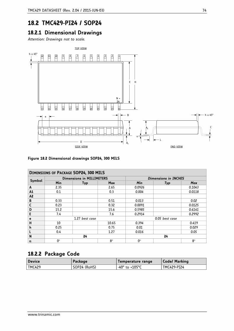
TMC429 DATASHEET (Rev. 2.04 / 2015-JUN-03) 74
www.trinamic.com
18.2 TMC429-PI24 / SOP24
18.2.1 Dimensional Drawings Attention: Drawings not to scale.
123
H
e
E
D
A
A1
h x 45°
B h x 45°
A2C
L
TOP VIEW
SIDE VIEW
456789101112
13 14 15 16 17 18 19 20 21 22 23
N = 24
24
END VIEW
α
Figure 18.2 Dimensional drawings SOP24, 300 MILS
DIMENSIONS OF PACKAGE SOP24, 300 MILS
Symbol Dimensions in MILLIMETERS Dimensions in INCHES
Min Typ Max Min Typ Max A 2.35 2.65 0.0926 0.1043 A1 0.1 0.3 0.004 0.0118 A2 B 0.33 0.51 0.013 0.02 C 0.23 0.32 0.0091 0.0125 D 15.2 15.6 0.5985 0.6141 E 7.4 7.6 0.2914 0.2992 e 1.27 best case 0.05 best case H 10 10.65 0.394 0.419 h 0.25 0.75 0.01 0.029 L 0.4 1.27 0.016 0.05 N 24 24 α 0° 8° 0° 8°
18.2.2 Package Code Device Package Temperature range Code/ Marking
TMC429 SOP24 (RoHS) -40° to +105°C TMC429-PI24

TMC429 DATASHEET (Rev. 2.04 / 2015-JUN-03) 75
www.trinamic.com
18.4 TMC429-I / SSOP16
18.4.1 Dimensional Drawings Attention: Drawings not to scale.
HE
h x 45° 123
16
8
9
e
D
A
A1
h x 45°
A2
L
WITH PLATING
b1
c1 c
b
BASE METAL
TOP VIEW
SIDE VIEW
C
B
4567
151413121110
END VIEW
LEAD (SIDE VIEW)
N=16
S
α
Figure 18.3 Dimensional drawings SSOP16, 150 MILS, 0.635mm (0.025 inch) pitch
DIMENSIONS OF PACKAGE SSOP16, 150 MILS
Symbol Dimensions in MILLIMETERS Dimensions in INCHES
Min Typ Max Min Typ Max A 1.55 1.63 1.73 0.061 0.064 0.068 A1 0.10 0.15 0.25 0.004 0.006 0.0098 A2 1.40 1.47 1.55 0.055 0.058 0.061 b 0.20 0.30 0.008 0.012 b1 0.20 0.25 0.28 0.008 0.010 0.011 c 0.18 0.25 0.007 0.010 c1 0.18 0.20 0.23 0.007 0.008 0.009 B 0.20 0.25 0.31 0.008 0.010 0.012 C 0.19 0.20 0.25 0.0075 0.008 0.0098 D 4.80 4.93 4.98 0.189 0.194 0.196 E 3.91 best case 0.154 best case e 0.635 best case 0.025 best case H 6.02 best case 0.237 best case h 0.25 0.33 0.41 0.010 0.013 0.016 L 0.41 0.635 0.89 0.016 0.025 0.035 N 16 16 S 0.051 0.114 0.178 0.0020 0.0045 0.0070 α 0° 5° 8° 0° 5° 8°
18.4.2 Package Code Device Package Temperature range Code/ Marking
TMC429 SSOP16 (RoHS) -40° to +105°C TMC429-I

TMC429 DATASHEET (Rev. 2.04 / 2015-JUN-03) 76
www.trinamic.com
19 Marking PRODUCT NAME TMC429-I Package SSOP16 – 150 MILS Date code WWYY (week WW and year YY) Lot number identifier LLLL Logo No
Zoomed Size
TMC429-ITrinamic
WWYYLLLL
PRODUCT NAME TMC429-LI Package QFN32 5mm * 5mm Date code WWYY (week WW and year YY) Lot number identifier LLLL Logo Yes
Zoomed Size
TRINAMICTMC429-LIWWYY LLLL
PRODUCT NAME TMC429-PI24 Package SOP24 – 300 MILS Date code WWYY (week WW and year YY) Lot number identifier LLLL Logo Yes
Zoomed Size
TMC429-PI24TrinamicWWYY LLLL

TMC429 DATASHEET (Rev. 2.04 / 2015-JUN-03) 77
www.trinamic.com
20 Compatibility Information: TMC429 and TMC428 The TMC429 is the 100% functional and pin compatible successor of the TMC428. The TMC429 can replace a TMC428 in existing hardware / software environments. There are some additional functions of the TMC429 which are mapped in register address ranges that were indicated reserved addresses for later versions. When these additional registers of the TMC429 are not accessed, the TMC429 behaves identically as a TMC428. Registers, which are added in the TMC429, are labeled with _429 (e.g. register if_configuration_429). The TMC429 has a step/direction interface that perfectly fits to the TRINAMIC stepper motor driver family TMC260, TMC261, and TMC262. The TMC429 has a higher clock frequency range than the TMC428: - The TMC428 can be clocked up to 16MHz. - The TMC429 can be clocked with up to 32MHz.
20.1 Signal Descriptions: TMC428 vs. TMC429 Please note, that the STEP/DIR interface of the TMC429 is not mentioned in this section because elder TMC428 applications always use SPI interface. All pin functions necessary for replacing the TMC428 by the TMC429 are described in this table. Pin TMC429 Pin TMC428
SSOP16 SOP24 TMC428
SOP24 TMC429
In/Out Description
Reset - - - - Internal power-on reset CLK 5 7 7 I Clock input nSCS_C 6 9 9 I Low active SPI chip select input driven from µC SCK_C 7 10 10 I Serial data clock input driven from µC SDI_C 8 11 11 I Serial data input driven from µC nINT_SDO_C SDO_C / nINT
9 14 14 O Serial data output to µC input / multiplexed nINTERRUPT output if communication with µC is idle (resp. nSCS_C = 1) SDO_C will never be high impedance, but this function can be added with a single gate 74HCT1G125 (see Figure 20.1). The TMC429 is equipped with an additional pin named SDOZ_C which becomes high impedance when nSCS_C=1.
nSCS_S_S2 nSCS_S
12 17 17 O SPI chip select signal to stepper motor driving chain
nSCS2_S3 nSCS2
- 18 18 O SPI chip select signal
nSCS3_D3 nSCS3
- 19 19 O SPI chip select signal
SCK_S_D1 SCK_S
11 16 16 O Serial data clock output to SPI stepper motor driver chain
SDO_S_S1 SDO_S
10 15 15 O Serial data output to SPI stepper motor driver chain
SDI_S_D2 SDI_S
16 23 23 I
Serial data input from SPI stepper motor driver chain (pull-up/-down resistor at SDI_S avoids high impedance; SDI_S input is the power-on default)
REF1 1 2 2 I Reference switch input 1 No internal pull-up R
REF2 2 3 3 I Reference switch input 2 No internal pull-up R
REF3 3 4 4 I Reference switch input 3 No internal pull-up R
V5 13 5, 20 5, 20 +5V supply / +3.3V supply V33 14 21 21 470nF ceramic capacitor pin / +3.3V supply GND 15 8, 22 8, 22 Ground

TMC429 DATASHEET (Rev. 2.04 / 2015-JUN-03) 78
www.trinamic.com
Pin TMC429 Pin TMC428
SSOP16 SOP24 TMC428
SOP24 TMC429
In/Out Description
TEST 4 6 6 I Must be connected to GND as close as possible to the chip
n.c. - 1, 12, 13, 24
- - Not connected pins
POSCMP n.c.
- n.c. 1 n.c. / O Position compare output for SOP24 / output for pos_comp function (TMC429 only)
SDOZ_C - n.c. 12 O / Z SDOZ_C becomes high impedance (Z) when nSCS_C=1 / The nINT signal is not mapped to SDOZ_C pin / The TMC429 provides a register for configuration of the pin nINT_SDO_C to give the nINT signal directly without multiplexing.
REFR1 - n.c. 24 I Reference switch right 1 input Only available for TMC429 in SOP24 package; internal pull-up R
REFR2 - n.c. 13 I Reference switch right 2 input Only available for TMC429 in SOP24 package; internal pull-up R
Note
When replacing a TMC428 in SOP24 package by a TMC429 in SOP24 package on an existing PCB make sure that the pins 1 and 12 are not connected on the PCB. These pins are outputs for the TMC429 in SOP24 package.
The TMC428-I in SSOP16 can be replaced by a TMC429-I without restrictions.
20.2 TMC428 SDO_C Output
SCK_S
SDO_S
SDI_S
nSCS_SREF2 REF3REF1
TEST GNDCLK V5V33
TMC429SCK_C
SDI_C
nSCS_C
SDOZ_C
SCK_C
SDI_C
nSCS_C
SDOZ_C
nINT_SDO_C can be configured as non-mulitplexed interrupt output
nINT_SDO_CnINTSCK_S
SDO_S
SDI_S
nSCS_SREF2 REF3REF1
TEST GNDCLK V5V33
TMC428SCK_C
SDI_C
nSCS_C
SDO_C
74HCT1G125
SCK_C
SDI_C
nSCS_C
SDOZ_C
nINT optional multiplexed interrupt output / Hint: disable µC Interrupt input during SPI access while nSCS_C is low
Figure 20.1 TMC428 SDO_C tristate output using a single gate 74HCT1G125. The TMC429 has a dedicated tristate output (SDOZ_C). nINT_SDO_C can be switched to nINT.
20.3 Unused Addresses
20.3.1 Unused Address (IDX=%1111) Reading the register gives back the actual status bits and 24 data bits set to 0. Writing to this register has no effect for the TMC428. This register address (IDX=%1111) within each stepper motor register block SMDA=%00, %01, %10 is unused for the TMC428.
20.3.2 Unused Addresses (JDX=%0100, %0101, %0110, %1001) There are unused addresses within the address range of the global parameter registers. Access to these addresses has no effect for the TMC428. However, access should be avoided, because this address space may be used for future devices. For the TMC429, the global registers ad addresses JDX=%0100, %0101, %0110, %1001) are used for TMC429 specific function. Some bits of the clk2_div (JDX=%1111) are used for the timing configuration in step/direction mode of the TMC429.
For the TMC429 some of the un-used addresses are used for additional registers of the TMC429. Additional registers of the TMC429 are named as <NAME>_429 to indicate that these have TMC429 specific functions that are not available for the TMC428.

TMC429 DATASHEET (Rev. 2.04 / 2015-JUN-03) 79
www.trinamic.com
20.4 General Timing Parameters The TMC429 has improved values when compared to TMC428. In this table modified timing values are summarized.
General timing parameters (TMC428 with EMI optimized output drivers)
Symbol Parameter Conditions Min Typ Max Unit
fCLK Operation frequency fCLK = 1 / tCLK 0 16 32 MHz tCLK Clock period Raising edge to rising
edge of CLK 31.25 ∞ ns
tCLK_L Clock time low 12.5 ∞ ns tCLK_H Clock time high 12.5 ∞ ns tRISE_I Input signal rise time 10% to 90% except TEST
pin 0.5 ∞ ns
tFALL_I Input signal fall time 90% to 10% except TEST pin
0.5 ∞ ns
tRISE_O_428 Output signal rise time 10% to 90% 3 ns tFALL_O_428 Output signal fall time 90% to 10% 3 ns tSU Setup time Relative to falling clock
edge at CLK 1 ns
tHD Hold time Relative to falling clock edge at CLK
1 ns
tPD_428 Propagation delay time 50% of rising edge of the clock CLK to the 50% of the output
1
5
ns
TMC429 DATASHEET (Rev. 2.04 / 2015-JUN-03) 80
www.trinamic.com
21 Disclaimer TRINAMIC Motion Control GmbH & Co. KG does not authorize or warrant any of its products for use in life support systems, without the specific written consent of TRINAMIC Motion Control GmbH & Co. KG. Life support systems are equipment intended to support or sustain life, and whose failure to perform, when properly used in accordance with instructions provided, can be reasonably expected to result in personal injury or death. Information given in this data sheet is believed to be accurate and reliable. However no responsibility is assumed for the consequences of its use nor for any infringement of patents or other rights of third parties which may result from its use. Specifications are subject to change without notice. All trademarks used are property of their respective owners.
22 ESD Sensitive Device The TMC429 is an ESD-sensitive CMOS device and sensitive to electrostatic discharge. Take special care to use adequate grounding of personnel and machines in manual handling. After soldering the devices to the board, ESD requirements are more relaxed. Failure to do so can result in defects or decreased reliability. PAD cells are designed to resist ESD voltages corresponding to Human Body Model (MIL-STD-883, with RC = 1 – 10 MΩ, RD = 1.5 KΩ, and CS = 100 pF).
Note: In a modern SMD manufacturing process, ESD voltages well below 100V are standard. A major source for ESD is hot-plugging the motor during operation.

TMC429 DATASHEET (Rev. 2.04 / 2015-JUN-03) 81
www.trinamic.com
23 Table of Figures Figure 1.1 TMC429 functional block diagram ................................................................................................................ 4 Figure 1.2 Application example using Step/Dir driver interface ............................................................................. 5 Figure 1.3 Application example using SPI driver interface ...................................................................................... 5 Figure 4.1 TMC429 pin out ............................................................................................................................................... 11 Figure 5.1 TMC429 within QFN32 package ................................................................................................................... 13 Figure 5.2 TMC429 / TMC26x outline for configuration via SPI and STEP/DIR for motion ............................ 13 Figure 5.3 TMC429 application environment with TMC429 in SSOP16 package ............................................... 14 Figure 5.4 Usage of drivers without serial data output (SDO) with TMC429 in SOP24 or in QFN32 packages ................................................................................................................................................................................ 14 Figure 6.1 Timing diagram of the serial µC interface .............................................................................................. 16 Figure 6.2 The TMC429 has a high impedance pin SDOZ_C. The nINT_SDO_C can be configured as non multiplexed interrupt output nINT if required. .......................................................................................................... 17 Figure 8.1 Velocity ramp parameters and velocity profiles .................................................................................... 24 Figure 8.2 Target position calculation, ramp generator, and pulse generator................................................. 28 Figure 8.3 Proportionality parameter p and outline of velocity profile(s) ......................................................... 30 Figure 8.4 Left switch and right switch for reference search and automatic stop function ....................... 33 Figure 8.5 Example of status bit mapping for a chain of three TMC246 or TMC249 ...................................... 40 Figure 8.6 Cover datagram example with 7 bits covering 7 bits of a 48 bit datagram ................................ 41 Figure 9.1 TMC429-LI has three right reference inputs. TMC429-PI24 has two right reference inputs. .... 49 Figure 9.2 Reference switch configuration left-side-only for mot1r=0 (and refmux=0) .................................. 50 Figure 9.3 Reference switch configuration two-one-zero for mot1r=1 (and refmux=0) .................................. 50 Figure 9.4 Reference switch multiplexing with 74HC157 (refmux=1) ................................................................... 51 Figure 9.5 Triple switch configuration left stop switch – reference switch – right stop switch ................ 51 Figure 9.6 Reference search ............................................................................................................................................. 52 Figure 9.7 Reference switch gateing for exact simultanous stepper motor start ........................................... 52 Figure 10.1 Step/Dir timing (en_sd = 1; step_half = 0) ............................................................................................. 53 Figure 11.1 Timing diagram of the serial stepper motor driver interface ......................................................... 54 Figure 11.2 Serially transmitted control and status signals between TMC429 and driver chain ................ 58 Figure 11.3 Microstep enhancement by introduction of a shape function ....................................................... 65 Figure 13.1 3 V operation (CMOS) vs. 5 V operation (TTL) ..................................................................................... 68 Figure 14.1 Operating principle of the power-on-reset ........................................................................................... 69 Figure 16.1 General timing parameters ........................................................................................................................ 72 Figure 18.1 Dimensional drawings of QFN32 ............................................................................................................. 73 Figure 18.2 Dimensional drawings SOP24, 300 MILS ............................................................................................... 74 Figure 18.3 Dimensional drawings SSOP16, 150 MILS, 0.635mm (0.025 inch) pitch ....................................... 75 Figure 20.1 TMC428 SDO_C tristate output using a single gate 74HCT1G125. The TMC429 has a dedicated tristate output (SDOZ_C). nINT_SDO_C can be switched to nINT. .................................................... 78

TMC429 DATASHEET (Rev. 2.04 / 2015-JUN-03) 82
www.trinamic.com
24 Revision History Version Date Author
LL – Lars Larsson
BD – Bernhard Dwersteg
SD – Sonja Dwersteg
Description
1.00 2009-DEC-08 LL - TMC429 Datasheet Rev. 1.00 based on TMC428 Datasheet Rev. 2.03 / December 18, 2009.
- Corrections: p = a_max / ( 128 * 2^( pulse_div – ramp_div ) ) p = a_max / ( 128 * 2^( ramp_div - pulse_div ) );
2010-MAY-05 LL - QFN32 package pinning added. - Hint added concerning changing of pluse_div while
VELOCITY_MODE or HOLD_MODE that might force am internal step pulse depending on the current position.
- DIL20 package of TMC428 removed. 2010-AUG-05 LL - Pin out GND @ 25 and n.c. @ 32 added for QFN32
package. - Pinning table updated with TMC428 SOP24 package
variant. - Hints added for new functions of the TMC429. - Section 20.3 Unused Addresses - Unused Address (IDX=%1111) , p. 78 and section
8.1.16USTEP_COUNT_429 (IDX=%1111) modified / added because this register was unused for the TMC428 but is a read / write register for the TMC429.
2010-AUG-26) LL - SDO_C renamed to iINT_SDC_C at package drawings. - SPI configuration outline added.
2010-SEP-10 LL - Figure 20.1 TMC428 SDO_C tristate output using a single gate 74HCT1G125. The TMC429 has a dedicated tristate output (SDOZ_C). nINT_SDO_C can be switched to nINT.
- Description of if_Configuration_429 finalized. - Step/direction timing figure and description added
(section 10 Step/Dir , page 53). - Short description of differences between TMC428 vs.
TMC429. - Section 12.2 Running a Motor with Start-Stop-Speed in
ramp_mode, page 67 new. 1.01 2010-OCT-10 LL - Marking (section 19, p. 76) updated.
- Timing parameter updated 1.02 2010-NOV-01 LL Pinning of SSOP16 (pin 10) package variant corrected. 1.03 2010-NOV-05 LL - TMC428 drawings (Figure 20.1, Figure 9.2, Figure 9.3,
Figure 9.1, Figure 9.4, Figure 9.7) updated concerning TMC428 / TMC429.
- Feature list updated concerning step direction interface; 1.04 2010-NOV-11 LL - Section 10 Step/Dir , page 53 equation tSTEP[µs]
corrected. 1.05 2010-DEC-06 LL - Position compare control register (pos_comp) and
associated output poscmp labelling unified. - TMC428 changed to TMC429 in text if necessary.
2011-APR-06
2011-MAY-17
2011-AUG-02
2011-DEC-15
LL - Preliminary removed and version date updated; no changes within the document itself.
- Hint concerning microstep frequency added in section 10, p. 53.
- Post address updated. - Hint concerning current scaling at rest added. - Typical current ISC32MHZ added and symbol ISC4MHZ429
corrected/changed to ISC8MHZ429. - Power-on default initialization of the SPI driver chain for

TMC429 DATASHEET (Rev. 2.04 / 2015-JUN-03) 83
www.trinamic.com
Version Date Author LL – Lars Larsson
BD – Bernhard Dwersteg
SD – Sonja Dwersteg
Description
2012-JAN-19
TMC236/TMC239/TMC246/TMC249 SPI stepper motor chain updated.
- TMC429 power-on reset (POR) default values added. - Hint concerning power-on defaults of sine wave table
added. 1.06 2012-JAN-27
2012-MAR-28
2012-MAY-22
LL - Section 12.2 Running a Motor with Start-Stop-Speed in ramp_mode item set X_TARGET := V_START_STOP corrected to set X_TARGET to desired position. Initialization of On-Chip RAM by µC after Power-On updated.
- Hint concerning frequency of SPI clock SCK relative to TMC429 clock fCLK added.
- Updated concerning dimensioning drawing at rising edge of direction signal (signal shape itself was correct).
1.07 2012-AUG-01 SD - Section 0 corrected: smda 0100. 2.00 2012-DEC-03 SD Amended datasheet version with new design. Several
changes. 2.01 2012-DEC-18 JP General DC characteristics changed 2.02 2013-NOV-04 SD - Application example in chapter 5.2 updated.
- USTEP_COUNT_429 description updated - Value ranges for X_TARGET and X_ACTUAL updated
(signed and unsigned are possible). - Chapter 1.2.1 (serial µC interface) corrected.
2.03 2015-MAR-10 BD - A_ACTUAL is signed, 12 bit (p. 22) 2.04 2015-JUN-03 BD Corrected meaning of RS bits in SPI status information field
25 References [TMC429+26x-EVAL] TMC429+26x-EVAL Manual / Evaluation board for S/D chipset (TMC429with
TMC260, TMC261, TMC262 and TMC424) [TMC429+TMC24x-EVAL] TMC429+TMC24x-EVAL Manual / Evaluation board for SPI chipset (TMC429,
TMC246, and TMC249)