motorola mc68030 - uvajesman/bigseti/ftp/microprocesadores/motorola/... · motorola mc68030...
TRANSCRIPT
MOTOROLA INC., 1992
MOTOROLAMC68030
ENHANCED 32-BITMICROPROCESSOR
USER’S MANUAL
Third Edition
MOTOROLA
MC68030 USER’S MANUAL
xxiii
PREFACE
The
MC68030 User's Manual
describes the capabilities, operation, and programming of theMC68030 32-bit second-generation enhanced microprocessor. The manual consists of thefollowing sections and appendix. For detailed information on the MC68030 instruction setrefer to M68000PM/AD,
M68000 Family Programmer's Reference Manual.
Section 1. Introduction
Section 2. Data Organization and Addressing Capabilities
Section 3. Instruction Set Summary
Section 4. Processing States
Section 5. Signal Description
Section 6. On-Chip Cache Memories
Section 7. Bus Operation
Section 8. Exception Processing
Section 9. Memory Management Unit
Section 10. Coprocessor Interface Description
Section 11. Instruction Execution Timing
Section 12. Applications Information
Section 13. Electrical Characteristics
Section 14. Ordering Information and Mechanical Data
Appendix A. M68000 Family Summary
Index
NOTE
In this manual, assertion and negation are used to specify forc-ing a signal to a particular state. In particular, assertion and as-sert refer to a signal that is active or true; negation and negateindicate a signal that is inactive or false. These terms are usedindependently of the voltage level (high or low) that they repre-sent.
The audience of this manual includes systems designers, systems programmers, andapplications programmers. Systems designers need some knowledge of all sections, withparticular emphasis on Sections 1, 5, 6, 7, 13, 14, and Appendix A. Designers whoimplement a coprocessor for their system also need a thorough knowledge of Section 10.
xxiv
MC68030 USER’S MANUAL
MOTOROLA
Systems programmers should become familiar with Sections 1, 2, 3, 4, 6, 8, 9, 11, andAppendix A. Applications programmers can find most of the information they need inSections 1, 2, 3, 4, 9, 11, 12, and Appendix A.
From a different viewpoint, the audience for this book consists of users of other M68000Family members and those who are not familiar with these microprocessors. Users of theother family members can find references to similarities to and differences from the otherMotorola microprocessors throughout the manual. However, Section 1 and Appendix Aspecifically identify the MC68030 within the rest of the family and contrast its differences.

MOTOROLA
MC68030 USER’S MANUAL
xxv
TABLE OF CONTENTS
ParagraphNumber
Title PageNumber
Section 1Introduction
1.1 Features . . . . . . . . . . . . . . . . . . . . . . . . . . . . . . . . . . . . . . . . . . . . . . . 1-31.2 MC68030 Extensions to the M68000 Family . . . . . . . . . . . . . . . . . . . 1-41.3 Programming Model . . . . . . . . . . . . . . . . . . . . . . . . . . . . . . . . . . . . . . 1-41.4 Data Types and Addressing Modes . . . . . . . . . . . . . . . . . . . . . . . . . . 1-101.5 Instruction Set Overview . . . . . . . . . . . . . . . . . . . . . . . . . . . . . . . . . . 1-101.6 Virtual Memory and Virtual Machine Concepts . . . . . . . . . . . . . . . . . 1-121.6.1 Virtual Memory . . . . . . . . . . . . . . . . . . . . . . . . . . . . . . . . . . . . . . . . 1-121.6.2 Virtual Machine . . . . . . . . . . . . . . . . . . . . . . . . . . . . . . . . . . . . . . . . 1-141.7 The Memory Management Unit . . . . . . . . . . . . . . . . . . . . . . . . . . . . . 1-151.8 Pipelined Architecture . . . . . . . . . . . . . . . . . . . . . . . . . . . . . . . . . . . . 1-161.9 The Cache Memories . . . . . . . . . . . . . . . . . . . . . . . . . . . . . . . . . . . . . 1-16
Section 2Data Organization and Addressing Capabilities
2.1 Instruction Operands . . . . . . . . . . . . . . . . . . . . . . . . . . . . . . . . . . . . . 2-12.2 Organization of Data in Registers . . . . . . . . . . . . . . . . . . . . . . . . . . . 2-22.2.1 Data Registers. . . . . . . . . . . . . . . . . . . . . . . . . . . . . . . . . . . . . . . . . 2-22.2.2 Address Registers . . . . . . . . . . . . . . . . . . . . . . . . . . . . . . . . . . . . . . 2-42.2.3 Control Registers. . . . . . . . . . . . . . . . . . . . . . . . . . . . . . . . . . . . . . . 2-42.3 Organization of Data in Memory. . . . . . . . . . . . . . . . . . . . . . . . . . . . . 2-52.4 Addressing Modes . . . . . . . . . . . . . . . . . . . . . . . . . . . . . . . . . . . . . . . 2-82.4.1 Data Register Direct Mode . . . . . . . . . . . . . . . . . . . . . . . . . . . . . . . 2-92.4.2 Address Register Direct Mode. . . . . . . . . . . . . . . . . . . . . . . . . . . . . 2-102.4.3 Address Register Indirect Mode . . . . . . . . . . . . . . . . . . . . . . . . . . . 2-102.4.4 Address Register Indirect with Postincrement Mode. . . . . . . . . . . . 2-102.4.5 Address Register Indirect with Predecrement Mode . . . . . . . . . . . . 2-112.4.6 Address Register Indirect with Displacement Mode . . . . . . . . . . . . 2-122.4.7 Address Register Indirect with Index (8-Bit Displacement) Mode . . 2-122.4.8 Address Register Indirect with Index (Base Displacement) Mode. . 2-132.4.9 Memory Indirect Postindexed Mode . . . . . . . . . . . . . . . . . . . . . . . . 2-142.4.10 Memory Indirect Preindexed Mode . . . . . . . . . . . . . . . . . . . . . . . . . 2-152.4.11 Program Counter Indirect with Displacement Mode . . . . . . . . . . . . 2-162.4.12 Program Counter Indirect with Index (8-Bit Displacement) Mode . . 2-162.4.13 Program Counter Indirect with Index (Base Displacement) Mode. . 2-172.4.14 Program Counter Memory Indirect Postindexed Mode . . . . . . . . . . 2-182.4.15 Program Counter Memory Indirect Preindexed Mode . . . . . . . . . . . 2-192.4.16 Absolute Short Addressing Mode . . . . . . . . . . . . . . . . . . . . . . . . . . 2-202.4.17 Absolute Long Addressing Mode. . . . . . . . . . . . . . . . . . . . . . . . . . . 2-202.4.18 Immediate Data . . . . . . . . . . . . . . . . . . . . . . . . . . . . . . . . . . . . . . . . 2-212.5 Effective Address Encoding Summary. . . . . . . . . . . . . . . . . . . . . . . . 2-22
xxvi
MC68030 USER’S MANUAL
MOTOROLA
TABLE OF CONTENTS
(
Continued
)
ParagraphNumber
Title PageNumber
2.6 Programmer`s View of Addressing Modes. . . . . . . . . . . . . . . . . . . . . 2-242.6.1 Addressing Capabilities . . . . . . . . . . . . . . . . . . . . . . . . . . . . . . . . . . 2-252.6.2 General Addressing Mode Summary . . . . . . . . . . . . . . . . . . . . . . . 2-312.7 M68000 Family Addressing Compatibility . . . . . . . . . . . . . . . . . . . . . 2-362.8 Other Data Structures . . . . . . . . . . . . . . . . . . . . . . . . . . . . . . . . . . . . 2-362.8.1 System Stack. . . . . . . . . . . . . . . . . . . . . . . . . . . . . . . . . . . . . . . . . . 2-362.8.2 User Program Stacks . . . . . . . . . . . . . . . . . . . . . . . . . . . . . . . . . . . 2-382.8.3 Queues . . . . . . . . . . . . . . . . . . . . . . . . . . . . . . . . . . . . . . . . . . . . . . 2-39
Section 3Instruction Set Summary
3.1 Instruction Format . . . . . . . . . . . . . . . . . . . . . . . . . . . . . . . . . . . . . . . 3-13.2 Instruction Summary . . . . . . . . . . . . . . . . . . . . . . . . . . . . . . . . . . . . . 3-23.2.1 Data Movement Instructions . . . . . . . . . . . . . . . . . . . . . . . . . . . . . . 3-43.2.2 Integer Arithmetic Instructions . . . . . . . . . . . . . . . . . . . . . . . . . . . . . 3-53.2.3 Logical Instructions . . . . . . . . . . . . . . . . . . . . . . . . . . . . . . . . . . . . . 3-63.2.4 Shift and Rotate Instructions . . . . . . . . . . . . . . . . . . . . . . . . . . . . . . 3-73.2.5 Bit Manipulation Instructions . . . . . . . . . . . . . . . . . . . . . . . . . . . . . . 3-83.2.6 Bit Field Operations . . . . . . . . . . . . . . . . . . . . . . . . . . . . . . . . . . . . . 3-93.2.7 Binary–coded Decimal Instructions . . . . . . . . . . . . . . . . . . . . . . . . . 3-103.2.8 Program Control Instructions. . . . . . . . . . . . . . . . . . . . . . . . . . . . . . 3-113.2.9 System Control Instructions. . . . . . . . . . . . . . . . . . . . . . . . . . . . . . . 3-123.2.10 Memory Management Unit Instructions. . . . . . . . . . . . . . . . . . . . . . 3-133.2.11 Multiprocessor Instructions . . . . . . . . . . . . . . . . . . . . . . . . . . . . . . . 3-133.3 Integer Condition Codes. . . . . . . . . . . . . . . . . . . . . . . . . . . . . . . . . . . 3-143.3.1 Condition Code Computation . . . . . . . . . . . . . . . . . . . . . . . . . . . . . 3-153.3.2 Conditional Tests. . . . . . . . . . . . . . . . . . . . . . . . . . . . . . . . . . . . . . . 3-173.4 Instruction Set Summary . . . . . . . . . . . . . . . . . . . . . . . . . . . . . . . . . . 3-183.5 Instruction Examples . . . . . . . . . . . . . . . . . . . . . . . . . . . . . . . . . . . . . 3-253.5.1 Using the CAS and CAS2 Instructions . . . . . . . . . . . . . . . . . . . . . . 3-253.5.2 Nested Subroutine Calls . . . . . . . . . . . . . . . . . . . . . . . . . . . . . . . . . 3-303.5.3 Bit Field Operations . . . . . . . . . . . . . . . . . . . . . . . . . . . . . . . . . . . . . 3-313.5.4 Pipeline Synchronization with the Nop Instruction. . . . . . . . . . . . . . 3-32
Section 4Processing States
4.1 Privilege Levels . . . . . . . . . . . . . . . . . . . . . . . . . . . . . . . . . . . . . . . . . 4-24.1.1 Supervisor Privilege Level . . . . . . . . . . . . . . . . . . . . . . . . . . . . . . . . 4-24.1.2 User Privilege Level. . . . . . . . . . . . . . . . . . . . . . . . . . . . . . . . . . . . . 4-34.1.3 Changing Privilege Level. . . . . . . . . . . . . . . . . . . . . . . . . . . . . . . . . 4-44.2 Address Space Types . . . . . . . . . . . . . . . . . . . . . . . . . . . . . . . . . . . . 4-54.3 Exception Processing. . . . . . . . . . . . . . . . . . . . . . . . . . . . . . . . . . . . . 4-6

MOTOROLA
MC68030 USER’S MANUAL
xxvii
TABLE OF CONTENTS
(
Continued
)
ParagraphNumber
Title PageNumber
4.3.1 Exception Vectors . . . . . . . . . . . . . . . . . . . . . . . . . . . . . . . . . . . . . . 4-64.3.2 Exception Stack Frame . . . . . . . . . . . . . . . . . . . . . . . . . . . . . . . . . . 4-7
Section 5Signal Description
5.1 Signal Index . . . . . . . . . . . . . . . . . . . . . . . . . . . . . . . . . . . . . . . . . . . . 5-25.2 Function Code Signals (FC0–FC2) . . . . . . . . . . . . . . . . . . . . . . . . . . 5-45.3 Address Bus (A0–A31). . . . . . . . . . . . . . . . . . . . . . . . . . . . . . . . . . . . 5-45.4 Data Bus (D0–D31) . . . . . . . . . . . . . . . . . . . . . . . . . . . . . . . . . . . . . . 5-45.5 Transfer Size Signals (SIZ0, SIZ1). . . . . . . . . . . . . . . . . . . . . . . . . . . 5-45.6 Bus Control Signals . . . . . . . . . . . . . . . . . . . . . . . . . . . . . . . . . . . . . . 5-55.6.1 Operand Cycle Start (OCS). . . . . . . . . . . . . . . . . . . . . . . . . . . . . . . 5-55.6.2 External Cycle Start (ECS) . . . . . . . . . . . . . . . . . . . . . . . . . . . . . . . 5-55.6.3 Read/Write (R/W) . . . . . . . . . . . . . . . . . . . . . . . . . . . . . . . . . . . . . . 5-55.6.4 Read-Modify-Write Cycle (RMC) . . . . . . . . . . . . . . . . . . . . . . . . . . . 5-55.6.5 Address Strobe (AS) . . . . . . . . . . . . . . . . . . . . . . . . . . . . . . . . . . . . 5-55.6.6 Data Strobe (DS) . . . . . . . . . . . . . . . . . . . . . . . . . . . . . . . . . . . . . . . 5-65.6.7 Data Buffer Enable (DBEN). . . . . . . . . . . . . . . . . . . . . . . . . . . . . . . 5-65.6.8 Data Transfer and Size Acknowledge (DSACK0, DSACK1) . . . . . . 5-65.6.9 Synchronous Termination (STERM) . . . . . . . . . . . . . . . . . . . . . . . . 5-65.7 Cache Control Signals . . . . . . . . . . . . . . . . . . . . . . . . . . . . . . . . . . . . 5-75.7.1 Cache Inhibit Input (CIIN) . . . . . . . . . . . . . . . . . . . . . . . . . . . . . . . . 5-75.7.2 Cache Inhibit Output (CIOUT) . . . . . . . . . . . . . . . . . . . . . . . . . . . . . 5-75.7.3 Cache Burst Request (CBREQ) . . . . . . . . . . . . . . . . . . . . . . . . . . . 5-75.7.4 Cache Burst Acknowledge (CBACK). . . . . . . . . . . . . . . . . . . . . . . . 5-75.8 Interrupt Control Signals. . . . . . . . . . . . . . . . . . . . . . . . . . . . . . . . . . . 5-85.8.1 Interrupt Priority Level Signals. . . . . . . . . . . . . . . . . . . . . . . . . . . . . 5-85.8.2 Interrupt Pending (IPEND). . . . . . . . . . . . . . . . . . . . . . . . . . . . . . . . 5-85.8.3 Autovector (AVEC) . . . . . . . . . . . . . . . . . . . . . . . . . . . . . . . . . . . . . 5-85.9 Bus Arbitration Control Signals . . . . . . . . . . . . . . . . . . . . . . . . . . . . . 5-85.9.1 Bus Request (BR) . . . . . . . . . . . . . . . . . . . . . . . . . . . . . . . . . . . . . . 5-85.9.2 Bus Grant (BG) . . . . . . . . . . . . . . . . . . . . . . . . . . . . . . . . . . . . . . . . 5-95.9.3 Bus Grant Acknowledge (BGACK) . . . . . . . . . . . . . . . . . . . . . . . . . 5-95.10 Bus Exception Control Signals . . . . . . . . . . . . . . . . . . . . . . . . . . . . . . 5-95.10.1 Reset (RESET) . . . . . . . . . . . . . . . . . . . . . . . . . . . . . . . . . . . . . . . . 5-95.10.2 Halt (HALT) . . . . . . . . . . . . . . . . . . . . . . . . . . . . . . . . . . . . . . . . . . . 5-95.10.3 Bus Error (BERR) . . . . . . . . . . . . . . . . . . . . . . . . . . . . . . . . . . . . . . 5-95.11 Emulator Support Signals. . . . . . . . . . . . . . . . . . . . . . . . . . . . . . . . . . 5-105.11.1 Cache Disable (CDIS) . . . . . . . . . . . . . . . . . . . . . . . . . . . . . . . . . . . 5-105.11.2 MMU Disable (MMUDIS) . . . . . . . . . . . . . . . . . . . . . . . . . . . . . . . . . 5-105.11.3 Pipeline Refill (REFILL) . . . . . . . . . . . . . . . . . . . . . . . . . . . . . . . . . . 5-105.11.4 Internal Microsequencer Status (STATUS) . . . . . . . . . . . . . . . . . . . 5-10

xxviii
MC68030 USER’S MANUAL
MOTOROLA
TABLE OF CONTENTS
(
Continued
)
ParagraphNumber
Title PageNumber
5.12 Clock (CLK) . . . . . . . . . . . . . . . . . . . . . . . . . . . . . . . . . . . . . . . . . . . . 5-115.13 Power Supply Connections . . . . . . . . . . . . . . . . . . . . . . . . . . . . . . . . 5-115.14 Signal Summary. . . . . . . . . . . . . . . . . . . . . . . . . . . . . . . . . . . . . . . . . 5-11
Section 6On-Chip Cache Memories
6.1 On-Chip Cache Organization and Operation . . . . . . . . . . . . . . . . . . . 6-36.1.1 Instruction Cache. . . . . . . . . . . . . . . . . . . . . . . . . . . . . . . . . . . . . . . 6-46.1.2 Data Cache . . . . . . . . . . . . . . . . . . . . . . . . . . . . . . . . . . . . . . . . . . . 6-66.1.2.1 Write Allocation . . . . . . . . . . . . . . . . . . . . . . . . . . . . . . . . . . . . . . 6-86.1.2.2 Read-Modify-Write Accesses. . . . . . . . . . . . . . . . . . . . . . . . . . . . 6-106.1.3 Cache Filling . . . . . . . . . . . . . . . . . . . . . . . . . . . . . . . . . . . . . . . . . . 6-106.1.3.1 Single Entry Mode . . . . . . . . . . . . . . . . . . . . . . . . . . . . . . . . . . . . 6-106.1.3.2 Burst Mode Filling . . . . . . . . . . . . . . . . . . . . . . . . . . . . . . . . . . . . 6-156.2 Cache Reset. . . . . . . . . . . . . . . . . . . . . . . . . . . . . . . . . . . . . . . . . . . . 6-206.3 Cache Control . . . . . . . . . . . . . . . . . . . . . . . . . . . . . . . . . . . . . . . . . . 6-206.3.1 Cache Control Register . . . . . . . . . . . . . . . . . . . . . . . . . . . . . . . . . . 6-206.3.1.1 Write Allocate. . . . . . . . . . . . . . . . . . . . . . . . . . . . . . . . . . . . . . . . 6-216.3.1.2 Data Burst Enable . . . . . . . . . . . . . . . . . . . . . . . . . . . . . . . . . . . . 6-216.3.1.3 Clear Data Cache . . . . . . . . . . . . . . . . . . . . . . . . . . . . . . . . . . . . 6-216.3.1.4 Clear Entry in Data Cache . . . . . . . . . . . . . . . . . . . . . . . . . . . . . . 6-216.3.1.5 Freeze Data Cache . . . . . . . . . . . . . . . . . . . . . . . . . . . . . . . . . . . 6-226.3.1.6 Enable Data Cache . . . . . . . . . . . . . . . . . . . . . . . . . . . . . . . . . . . 6-226.3.1.7 Instruction Burst Enable. . . . . . . . . . . . . . . . . . . . . . . . . . . . . . . . 6-226.3.1.8 Clear Instruction Cache . . . . . . . . . . . . . . . . . . . . . . . . . . . . . . . . 6-226.3.1.9 Clear Entry in Instruction Cache . . . . . . . . . . . . . . . . . . . . . . . . . 6-226.3.1.10 Freeze Instruction Cache. . . . . . . . . . . . . . . . . . . . . . . . . . . . . . . 6-236.3.1.11 Enable Instruction Cache. . . . . . . . . . . . . . . . . . . . . . . . . . . . . . . 6-236.3.2 Cache Address Register . . . . . . . . . . . . . . . . . . . . . . . . . . . . . . . . . 6-23
Section 7Bus Operation
7.1 Bus Transfer Signals . . . . . . . . . . . . . . . . . . . . . . . . . . . . . . . . . . . . . 7-17.1.1 Bus Control Signals . . . . . . . . . . . . . . . . . . . . . . . . . . . . . . . . . . . . . 7-37.1.2 Address Bus . . . . . . . . . . . . . . . . . . . . . . . . . . . . . . . . . . . . . . . . . . 7-47.1.3 Address Strobe . . . . . . . . . . . . . . . . . . . . . . . . . . . . . . . . . . . . . . . . 7-47.1.4 Data Bus . . . . . . . . . . . . . . . . . . . . . . . . . . . . . . . . . . . . . . . . . . . . . 7-57.1.5 Data Strobe . . . . . . . . . . . . . . . . . . . . . . . . . . . . . . . . . . . . . . . . . . . 7-57.1.6 Data Buffer Enable . . . . . . . . . . . . . . . . . . . . . . . . . . . . . . . . . . . . . 7-57.1.7 Bus Cycle Termination Signals . . . . . . . . . . . . . . . . . . . . . . . . . . . . 7-57.2 Data Transfer Mechanism . . . . . . . . . . . . . . . . . . . . . . . . . . . . . . . . . 7-67.2.1 Dynamic Bus Sizing. . . . . . . . . . . . . . . . . . . . . . . . . . . . . . . . . . . . . 7-6
MOTOROLA
MC68030 USER’S MANUAL
xxix
TABLE OF CONTENTS
(
Continued
)
ParagraphNumber
Title PageNumber
7.2.2 Misaligned Operands. . . . . . . . . . . . . . . . . . . . . . . . . . . . . . . . . . . . 7-137.2.3 Effects of Dynamic Bus Sizing and Operand Misalignment . . . . . . 7-197.2.4 Address, Size, and Data Bus Relationships . . . . . . . . . . . . . . . . . . 7-227.2.5 MC68030 versus MC68020 Dynamic Bus Sizing . . . . . . . . . . . . . . 7-247.2.6 Cache Filling . . . . . . . . . . . . . . . . . . . . . . . . . . . . . . . . . . . . . . . . . . 7-247.2.7 Cache Interactions. . . . . . . . . . . . . . . . . . . . . . . . . . . . . . . . . . . . . . 7-267.2.8 Asynchronous Operation . . . . . . . . . . . . . . . . . . . . . . . . . . . . . . . . . 7-277.2.9 Synchronous Operation with DSACKx . . . . . . . . . . . . . . . . . . . . . . 7-287.2.10 Synchronous Operation with STERM . . . . . . . . . . . . . . . . . . . . . . . 7-297.3 Data Transfer Cycles . . . . . . . . . . . . . . . . . . . . . . . . . . . . . . . . . . . . . 7-307.3.1 Asynchronous Read Cycle . . . . . . . . . . . . . . . . . . . . . . . . . . . . . . . 7-317.3.2 Asynchronous Write Cycle . . . . . . . . . . . . . . . . . . . . . . . . . . . . . . . 7-377.3.3 Asynchronous Read-Modify-Write Cycle. . . . . . . . . . . . . . . . . . . . . 7-437.3.4 Synchronous Read Cycle . . . . . . . . . . . . . . . . . . . . . . . . . . . . . . . . 7-487.3.5 Synchronous Write Cycle . . . . . . . . . . . . . . . . . . . . . . . . . . . . . . . . 7-517.3.6 Synchronous Read-Modify-Write Cycle. . . . . . . . . . . . . . . . . . . . . . 7-547.3.7 Burst Operation Cycles . . . . . . . . . . . . . . . . . . . . . . . . . . . . . . . . . . 7-597.4 CPU Space Cycles. . . . . . . . . . . . . . . . . . . . . . . . . . . . . . . . . . . . . . . 7-687.4.1 Interrupt Acknowledge Bus Cycles . . . . . . . . . . . . . . . . . . . . . . . . . 7-697.4.1.1 Interrupt Acknowledge Cycle — Terminated Normally . . . . . . . . 7-707.4.1.2 Autovector Interrupt Acknowledge Cycle . . . . . . . . . . . . . . . . . . . 7-717.4.1.3 Spurious Interrupt Cycle . . . . . . . . . . . . . . . . . . . . . . . . . . . . . . . 7-747.4.2 Breakpoint Acknowledge Cycle . . . . . . . . . . . . . . . . . . . . . . . . . . . . 7-747.4.3 Coprocessor Communication Cycles . . . . . . . . . . . . . . . . . . . . . . . 7-747.5 Bus Exception Control Cycles . . . . . . . . . . . . . . . . . . . . . . . . . . . . . . 7-757.5.1 Bus Errors . . . . . . . . . . . . . . . . . . . . . . . . . . . . . . . . . . . . . . . . . . . . 7-827.5.2 Retry Operation . . . . . . . . . . . . . . . . . . . . . . . . . . . . . . . . . . . . . . . . 7-897.5.3 Halt Operation . . . . . . . . . . . . . . . . . . . . . . . . . . . . . . . . . . . . . . . . . 7-917.5.4 Double Bus Fault . . . . . . . . . . . . . . . . . . . . . . . . . . . . . . . . . . . . . . . 7-947.6 Bus Synchronization. . . . . . . . . . . . . . . . . . . . . . . . . . . . . . . . . . . . . . 7-957.7 Bus Arbitration . . . . . . . . . . . . . . . . . . . . . . . . . . . . . . . . . . . . . . . . . . 7-967.7.1 Bus Request . . . . . . . . . . . . . . . . . . . . . . . . . . . . . . . . . . . . . . . . . . 7-987.7.2 Bus Grant . . . . . . . . . . . . . . . . . . . . . . . . . . . . . . . . . . . . . . . . . . . . 7-997.7.3 Bus Grant Acknowledge . . . . . . . . . . . . . . . . . . . . . . . . . . . . . . . . . 7-1007.7.4 Bus Arbitration Control . . . . . . . . . . . . . . . . . . . . . . . . . . . . . . . . . . 7-1007.8 Reset Operation . . . . . . . . . . . . . . . . . . . . . . . . . . . . . . . . . . . . . . . . . 7-103
Section 8Exception Processing
8.1 Exception Processing Sequence . . . . . . . . . . . . . . . . . . . . . . . . . . . . 8-18.1.1 Reset Exception . . . . . . . . . . . . . . . . . . . . . . . . . . . . . . . . . . . . . . . 8-58.1.2 Bus Error Exception. . . . . . . . . . . . . . . . . . . . . . . . . . . . . . . . . . . . . 8-7
xxx
MC68030 USER’S MANUAL
MOTOROLA
TABLE OF CONTENTS
(
Continued
)
ParagraphNumber
Title PageNumber
8.1.3 Address Error Exception . . . . . . . . . . . . . . . . . . . . . . . . . . . . . . . . . 8-88.1.4 Instruction Trap Exception. . . . . . . . . . . . . . . . . . . . . . . . . . . . . . . . 8-98.1.5 Illegal Instruction and Unimplemented Instruction Exceptions . . . . 8-98.1.6 Privilege Violation Exception . . . . . . . . . . . . . . . . . . . . . . . . . . . . . . 8-118.1.7 Trace Exception. . . . . . . . . . . . . . . . . . . . . . . . . . . . . . . . . . . . . . . . 8-128.1.8 Format Error Exception . . . . . . . . . . . . . . . . . . . . . . . . . . . . . . . . . . 8-148.1.9 Interrupt Exceptions. . . . . . . . . . . . . . . . . . . . . . . . . . . . . . . . . . . . . 8-148.1.10 MMU Configuration Exception. . . . . . . . . . . . . . . . . . . . . . . . . . . . . 8-218.1.11 Breakpoint Instruction Exception . . . . . . . . . . . . . . . . . . . . . . . . . . . 8-228.1.12 Multiple Exceptions . . . . . . . . . . . . . . . . . . . . . . . . . . . . . . . . . . . . . 8-238.1.13 Return from Exception. . . . . . . . . . . . . . . . . . . . . . . . . . . . . . . . . . . 8-248.2 Bus Fault Recovery . . . . . . . . . . . . . . . . . . . . . . . . . . . . . . . . . . . . . . 8-278.2.1 Special Status Word (SSW) . . . . . . . . . . . . . . . . . . . . . . . . . . . . . . 8-288.2.2 Using Software to Complete the Bus Cycles. . . . . . . . . . . . . . . . . . 8-298.2.3 Completing the Bus Cycles with Rte . . . . . . . . . . . . . . . . . . . . . . . . 8-318.3 Coprocessor Considerations . . . . . . . . . . . . . . . . . . . . . . . . . . . . . . . 8-328.4 Exception Stack Frame Formats . . . . . . . . . . . . . . . . . . . . . . . . . . . . 8-32
Section 9Memory Management Unit
9.1 Translation Table Structure . . . . . . . . . . . . . . . . . . . . . . . . . . . . . . . . 9-69.1.1 Translation Control . . . . . . . . . . . . . . . . . . . . . . . . . . . . . . . . . . . . . 9-89.1.2 Translation Table Descriptors . . . . . . . . . . . . . . . . . . . . . . . . . . . . . 9-109.2 Address Translation . . . . . . . . . . . . . . . . . . . . . . . . . . . . . . . . . . . . . . 9-139.2.1 General Flow for Address Translation . . . . . . . . . . . . . . . . . . . . . . . 9-139.2.2 Effect of RESET On MMU . . . . . . . . . . . . . . . . . . . . . . . . . . . . . . . . 9-159.2.3 Effect of MMUDIS On Address Translation . . . . . . . . . . . . . . . . . . . 9-159.3 Transparent Translation . . . . . . . . . . . . . . . . . . . . . . . . . . . . . . . . . . . 9-169.4 Address Translation Cache . . . . . . . . . . . . . . . . . . . . . . . . . . . . . . . . 9-179.5 Translation Table Details . . . . . . . . . . . . . . . . . . . . . . . . . . . . . . . . . . 9-209.5.1 Descriptor Details . . . . . . . . . . . . . . . . . . . . . . . . . . . . . . . . . . . . . . 9-209.5.1.1 Descriptor Field Definitions . . . . . . . . . . . . . . . . . . . . . . . . . . . . . 9-209.5.1.2 Root Pointer Descriptor . . . . . . . . . . . . . . . . . . . . . . . . . . . . . . . . 9-239.5.1.3 Short-Format Table Descriptor . . . . . . . . . . . . . . . . . . . . . . . . . . 9-249.5.1.4 Long-Fomat Table Descriptor . . . . . . . . . . . . . . . . . . . . . . . . . . . 9-249.5.1.5 Short-Format Early Termination Page Descriptor . . . . . . . . . . . . 9-259.5.1.6 Long-Format Early Termination Page Descriptor . . . . . . . . . . . . 9-259.5.1.7 Short-Format Page Descriptor . . . . . . . . . . . . . . . . . . . . . . . . . . . 9-269.5.1.8 Long-Format Page Descriptor . . . . . . . . . . . . . . . . . . . . . . . . . . . 9-269.5.1.9 Short-Format Invalid Descriptor . . . . . . . . . . . . . . . . . . . . . . . . . . 9-269.5.1.10 Long-Format Indirect Descriptor . . . . . . . . . . . . . . . . . . . . . . . . . 9-279.5.1.11 Short-Format Indirect Descriptor . . . . . . . . . . . . . . . . . . . . . . . . . 9-27

xxxi
MC68030 USER’S MANUAL
MOTOROLA
TABLE OF CONTENTS
(
Concluded
)
ParagraphNumber
Title PageNumber
9.5.1.12 Long-Format Indirect Descriptor . . . . . . . . . . . . . . . . . . . . . . . . . 9-289.5.2 General Table Search . . . . . . . . . . . . . . . . . . . . . . . . . . . . . . . . . . . 9-289.5.3 Variations in Translation Table Structure . . . . . . . . . . . . . . . . . . . . 9-339.5.3.1 Early Termination and Contiguous Memory. . . . . . . . . . . . . . . . . 9-339.5.3.2 Indirection . . . . . . . . . . . . . . . . . . . . . . . . . . . . . . . . . . . . . . . . . . 9-349.5.3.3 Table Sharing Between Tasks. . . . . . . . . . . . . . . . . . . . . . . . . . . 9-379.5.3.4 Paging of Tables . . . . . . . . . . . . . . . . . . . . . . . . . . . . . . . . . . . . . 9-379.5.3.5 Dynamic Allocation of Tables. . . . . . . . . . . . . . . . . . . . . . . . . . . . 9-409.5.4 Detail of Table Search Operations . . . . . . . . . . . . . . . . . . . . . . . . . 9-409.5.5 Protection . . . . . . . . . . . . . . . . . . . . . . . . . . . . . . . . . . . . . . . . . . . . 9-439.5.5.1 Function Code Lookup. . . . . . . . . . . . . . . . . . . . . . . . . . . . . . . . . 9-459.5.5.2 Supervisor Translation Tree. . . . . . . . . . . . . . . . . . . . . . . . . . . . . 9-489.5.5.3 Supervisor Only . . . . . . . . . . . . . . . . . . . . . . . . . . . . . . . . . . . . . . 9-489.5.5.4 Write Protect . . . . . . . . . . . . . . . . . . . . . . . . . . . . . . . . . . . . . . . . 9-489.6 MC68030 and MC68851 Mmu Differences . . . . . . . . . . . . . . . . . . . . 9-519.7 Registers . . . . . . . . . . . . . . . . . . . . . . . . . . . . . . . . . . . . . . . . . . . . . . 9-529.7.1 Root Pointer Registers . . . . . . . . . . . . . . . . . . . . . . . . . . . . . . . . . . 9-529.7.2 Translation Control Register . . . . . . . . . . . . . . . . . . . . . . . . . . . . . . 9-549.7.3 Transparent Translation Registers . . . . . . . . . . . . . . . . . . . . . . . . . 9-579.7.4 MMU Status Register . . . . . . . . . . . . . . . . . . . . . . . . . . . . . . . . . . . 9-599.7.5 Register Programming Considerations . . . . . . . . . . . . . . . . . . . . . . 9-619.7.5.1 Register Side Effects . . . . . . . . . . . . . . . . . . . . . . . . . . . . . . . . . . 9-619.7.5.2 MMU Status Register Decoding. . . . . . . . . . . . . . . . . . . . . . . . . . 9-619.7.5.3 MMU Configuration Exception . . . . . . . . . . . . . . . . . . . . . . . . . . . 9-629.8 Mmu Instructions . . . . . . . . . . . . . . . . . . . . . . . . . . . . . . . . . . . . . . . . 9-639.9 Defining and Using Page Tables in An Operating System. . . . . . . . . 9-659.9.1 Root Pointer Registers . . . . . . . . . . . . . . . . . . . . . . . . . . . . . . . . . . 9-659.9.2 Task Memory Map Definition. . . . . . . . . . . . . . . . . . . . . . . . . . . . . . 9-669.9.3 Impact of MMU Features On Table Definition . . . . . . . . . . . . . . . . . 9-689.9.3.1 Number of Table Levels. . . . . . . . . . . . . . . . . . . . . . . . . . . . . . . . 9-689.9.3.2 Initial Shift Count . . . . . . . . . . . . . . . . . . . . . . . . . . . . . . . . . . . . . 9-699.9.3.3 Limit Fields. . . . . . . . . . . . . . . . . . . . . . . . . . . . . . . . . . . . . . . . . . 9-709.9.3.4 Early Termination Page Descriptors . . . . . . . . . . . . . . . . . . . . . . 9-709.9.3.5 Indirect Descriptors . . . . . . . . . . . . . . . . . . . . . . . . . . . . . . . . . . . 9-719.9.3.6 Using Unused Descriptor Bits . . . . . . . . . . . . . . . . . . . . . . . . . . . 9-719.10 An Example of Paging Implementation in an Operating System . . . . 9-729.10.1 System Description . . . . . . . . . . . . . . . . . . . . . . . . . . . . . . . . . . . . . 9-729.10.2 Allocation Routines . . . . . . . . . . . . . . . . . . . . . . . . . . . . . . . . . . . . . 9-789.10.3 Bus Error Handler Routine . . . . . . . . . . . . . . . . . . . . . . . . . . . . . . . 9-82
Section 10Coprocessor Interface Description
xxxii
MC68030 USER’S MANUAL
MOTOROLA
TABLE OF CONTENTS
(
Continued
)
ParagraphNumber
Title PageNumber
10.1 Introduction. . . . . . . . . . . . . . . . . . . . . . . . . . . . . . . . . . . . . . . . . . . . . 10-110.1.1 Interface Features . . . . . . . . . . . . . . . . . . . . . . . . . . . . . . . . . . . . . . 10-210.1.2 Concurrent Operation Support . . . . . . . . . . . . . . . . . . . . . . . . . . . . 10-310.1.3 Coprocessor Instruction Format . . . . . . . . . . . . . . . . . . . . . . . . . . . 10-410.1.4 Coprocessor System Interface . . . . . . . . . . . . . . . . . . . . . . . . . . . . 10-510.1.4.1 Coprocessor Classification . . . . . . . . . . . . . . . . . . . . . . . . . . . . . 10-510.1.4.2 Processor-Coprocessor Interface . . . . . . . . . . . . . . . . . . . . . . . . 10-610.1.4.3 Coprocessor Interface Register Selection. . . . . . . . . . . . . . . . . . 10-810.2 Coprocessor Instruction Types. . . . . . . . . . . . . . . . . . . . . . . . . . . . . . 10-910.2.1 Coprocessor General Instructions . . . . . . . . . . . . . . . . . . . . . . . . . . 10-910.2.1.1 Format . . . . . . . . . . . . . . . . . . . . . . . . . . . . . . . . . . . . . . . . . . . . . 10-1010.2.1.2 Protocol.. . . . . . . . . . . . . . . . . . . . . . . . . . . . . . . . . . . . . . . . . . . . 10-1110.2.2 Coprocessor Conditional Instructions . . . . . . . . . . . . . . . . . . . . . . . 10-1210.2.2.1 Branch On Coprocessor Condition Instruction. . . . . . . . . . . . . . . 10-1310.2.2.1.1 Format. . . . . . . . . . . . . . . . . . . . . . . . . . . . . . . . . . . . . . . . . . . 10-1410.2.2.1.2 Protocol. . . . . . . . . . . . . . . . . . . . . . . . . . . . . . . . . . . . . . . . . . 10-1510.2.2.2 Set On Coprocessor Condition Instruction. . . . . . . . . . . . . . . . . . 10-1510.2.2.2.1 Format . . . . . . . . . . . . . . . . . . . . . . . . . . . . . . . . . . . . . . . . . . . 10-1510.2.2.2.2 Protocol. . . . . . . . . . . . . . . . . . . . . . . . . . . . . . . . . . . . . . . . . . 10-1610.2.2.3 Test Coprocessor Condition, Decrement and Branch Instruction 10-1710.2.2.3.1 Format . . . . . . . . . . . . . . . . . . . . . . . . . . . . . . . . . . . . . . . . . . . 10-1710.2.2.3.2 Protocol . . . . . . . . . . . . . . . . . . . . . . . . . . . . . . . . . . . . . . . . . . 10-1810.2.2.4 Trap On Coprocessor Condition. . . . . . . . . . . . . . . . . . . . . . . . . . 10-1810.2.2.4.1 Format . . . . . . . . . . . . . . . . . . . . . . . . . . . . . . . . . . . . . . . . . . . 10-1810.2.2.4.2 Protocol . . . . . . . . . . . . . . . . . . . . . . . . . . . . . . . . . . . . . . . . . . 10-1910.2.3 Coprocessor Save and Restore Instructions . . . . . . . . . . . . . . . . . . 10-2010.2.3.1 Coprocessor Internal State Frames. . . . . . . . . . . . . . . . . . . . . . . 10-2010.2.3.2 Coprocessor Format Words. . . . . . . . . . . . . . . . . . . . . . . . . . . . . 10-2210.2.3.2.1 Empty/Reset Format Word. . . . . . . . . . . . . . . . . . . . . . . . . . . . 10-2210.2.3.2.2 Not Ready Format Word.. . . . . . . . . . . . . . . . . . . . . . . . . . . . . 10-2310.2.3.2.3 Invalid Format Word . . . . . . . . . . . . . . . . . . . . . . . . . . . . . . . . 10-2310.2.3.2.4 Valid Format Word. . . . . . . . . . . . . . . . . . . . . . . . . . . . . . . . . . 10-2410.2.3.3 Coprocessor Context Save Instruction . . . . . . . . . . . . . . . . . . . . 10-2410.2.3.3.1 Format . . . . . . . . . . . . . . . . . . . . . . . . . . . . . . . . . . . . . . . . . . . 10-2410.2.3.3.2 Protocol . . . . . . . . . . . . . . . . . . . . . . . . . . . . . . . . . . . . . . . . . . 10-2510.2.3.4 Coprocessor Context Restore Instruction. . . . . . . . . . . . . . . . . . . 10-2710.2.3.4.1 Format . . . . . . . . . . . . . . . . . . . . . . . . . . . . . . . . . . . . . . . . . . . 10-2710.2.3.4.2 Protocol. . . . . . . . . . . . . . . . . . . . . . . . . . . . . . . . . . . . . . . . . . 10-2810.3 Coprocessor Interface Register Set . . . . . . . . . . . . . . . . . . . . . . . . . . 10-2910.3.1 Response CIR . . . . . . . . . . . . . . . . . . . . . . . . . . . . . . . . . . . . . . . . . 10-2910.3.2 Control CIR . . . . . . . . . . . . . . . . . . . . . . . . . . . . . . . . . . . . . . . . . . . 10-3010.3.3 Save CIR . . . . . . . . . . . . . . . . . . . . . . . . . . . . . . . . . . . . . . . . . . . . . 10-30
MOTOROLA
MC68030 USER’S MANUAL
xxxiii
TABLE OF CONTENTS
(
Continued
)
ParagraphNumber
Title PageNumber
10.3.4 Restore CIR. . . . . . . . . . . . . . . . . . . . . . . . . . . . . . . . . . . . . . . . . . . 10-3110.3.5 Operation Word CIR . . . . . . . . . . . . . . . . . . . . . . . . . . . . . . . . . . . . 10-3110.3.6 Command CIR. . . . . . . . . . . . . . . . . . . . . . . . . . . . . . . . . . . . . . . . . 10-3110.3.7 Condition CIR . . . . . . . . . . . . . . . . . . . . . . . . . . . . . . . . . . . . . . . . . 10-3110.3.8 Operand CIR . . . . . . . . . . . . . . . . . . . . . . . . . . . . . . . . . . . . . . . . . . 10-3210.3.9 Register Select CIR . . . . . . . . . . . . . . . . . . . . . . . . . . . . . . . . . . . . . 10-3210.3.10 Instruction Address CIR. . . . . . . . . . . . . . . . . . . . . . . . . . . . . . . . . . 10-3310.3.11 Operand Address CIR . . . . . . . . . . . . . . . . . . . . . . . . . . . . . . . . . . . 10-3310.4 Coprocessor Response Primitives . . . . . . . . . . . . . . . . . . . . . . . . . . . 10-3310.4.1 ScanPC . . . . . . . . . . . . . . . . . . . . . . . . . . . . . . . . . . . . . . . . . . . . . . 10-3410.4.2 Coprocessor Response Primitive General Format . . . . . . . . . . . . . 10-3510.4.3 Busy Primitive . . . . . . . . . . . . . . . . . . . . . . . . . . . . . . . . . . . . . . . . . 10-3610.4.4 Null Primitive . . . . . . . . . . . . . . . . . . . . . . . . . . . . . . . . . . . . . . . . . . 10-3710.4.5 Supervisor Check Primitive . . . . . . . . . . . . . . . . . . . . . . . . . . . . . . . 10-4010.4.6 Transfer Operation Word Primitive . . . . . . . . . . . . . . . . . . . . . . . . . 10-4010.4.7 Transfer from Instruction Stream Primitive . . . . . . . . . . . . . . . . . . . 10-4110.4.8 Evaluate and Transfer Effective Address Primitive . . . . . . . . . . . . . 10-4210.4.9 Evaluate Effective Address and Transfer Data Primitive. . . . . . . . . 10-4310.4.10 Write to Previously Evaluated Effective Address Primitive . . . . . . . 10-4610.4.11 Take Address and Transfer Data Primitive . . . . . . . . . . . . . . . . . . . 10-4810.4.12 Transfer to/from Top of Stack Primitive . . . . . . . . . . . . . . . . . . . . . . 10-4910.4.13 Transfer Single Main Processor Register Primitive . . . . . . . . . . . . . 10-5010.4.14 Transfer Main Processor Control Register Primitive . . . . . . . . . . . . 10-5010.4.15 Transfer Multiple Main Processor Registers Primitive. . . . . . . . . . . 10-5210.4.16 Transfer Multiple Coprocessor Registers Primitive . . . . . . . . . . . . . 10-5210.4.17 Transfer Status Register and ScanPC Primitive . . . . . . . . . . . . . . . 10-5510.4.18 Take Pre-Instruction Exception Primitive. . . . . . . . . . . . . . . . . . . . . 10-5610.4.19 Take Mid-Instruction Exception Primitive . . . . . . . . . . . . . . . . . . . . 10-5810.4.20 Take Post-Instruction Exception Primitive . . . . . . . . . . . . . . . . . . . . 10-6010.5 Exceptions . . . . . . . . . . . . . . . . . . . . . . . . . . . . . . . . . . . . . . . . . . . . . 10-6110.5.1 Coprocessor-Detected Exceptions . . . . . . . . . . . . . . . . . . . . . . . . . 10-6110.5.1.1 Coprocessor-Detected Protocol Violations . . . . . . . . . . . . . . . . . 10-6210.5.1.2 Coprocessor-Detected Illegal Command or Condition Words . . . 10-6310.5.1.3 Coprocessor Data-Processing Exceptions . . . . . . . . . . . . . . . . . 10-6310.5.1.4 Coprocessor System-Related Exceptions . . . . . . . . . . . . . . . . . . 10-6410.5.1.5 Format Errors. . . . . . . . . . . . . . . . . . . . . . . . . . . . . . . . . . . . . . . . 10-6410.5.2 Main-Processor-Detected Exceptions . . . . . . . . . . . . . . . . . . . . . . . 10-6510.5.2.1 Protocol Violations . . . . . . . . . . . . . . . . . . . . . . . . . . . . . . . . . . . . 10-6510.5.2.2 F-Line Emulator Exceptions. . . . . . . . . . . . . . . . . . . . . . . . . . . . . 10-6810.5.2.3 Privilege Violations. . . . . . . . . . . . . . . . . . . . . . . . . . . . . . . . . . . . 10-6910.5.2.4 cpTRAPcc Instruction Traps . . . . . . . . . . . . . . . . . . . . . . . . . . . . 10-6910.5.2.5 Trace Exceptions . . . . . . . . . . . . . . . . . . . . . . . . . . . . . . . . . . . . . 10-70
xxxiv
MC68030 USER’S MANUAL
MOTOROLA
TABLE OF CONTENTS
(
Continued
)
ParagraphNumber
Title PageNumber
10.5.2.6 Interrupts . . . . . . . . . . . . . . . . . . . . . . . . . . . . . . . . . . . . . . . . . . . 10-7110.5.2.7 Format Errors. . . . . . . . . . . . . . . . . . . . . . . . . . . . . . . . . . . . . . . . 10-7110.5.2.8 Address and Bus Errors. . . . . . . . . . . . . . . . . . . . . . . . . . . . . . . . 10-7210.5.3 Coprocessor Reset . . . . . . . . . . . . . . . . . . . . . . . . . . . . . . . . . . . . . 10-7210.6 Coprocessor Summary. . . . . . . . . . . . . . . . . . . . . . . . . . . . . . . . . . . . 10-72
Section 11Instruction Execution Timing
11.1 Performance Tradeoffs. . . . . . . . . . . . . . . . . . . . . . . . . . . . . . . . . . . . 11-111.2 Resource Scheduling . . . . . . . . . . . . . . . . . . . . . . . . . . . . . . . . . . . . . 11-211.2.1 Microsequencer . . . . . . . . . . . . . . . . . . . . . . . . . . . . . . . . . . . . . . . . 11-211.2.2 Instruction Pipe . . . . . . . . . . . . . . . . . . . . . . . . . . . . . . . . . . . . . . . . 11-211.2.3 Instruction Cache. . . . . . . . . . . . . . . . . . . . . . . . . . . . . . . . . . . . . . . 11-411.2.4 Data Cache . . . . . . . . . . . . . . . . . . . . . . . . . . . . . . . . . . . . . . . . . . . 11-411.2.5 Bus Controller Resources . . . . . . . . . . . . . . . . . . . . . . . . . . . . . . . . 11-411.2.5.1 Instruction Fetch Pending Buffer . . . . . . . . . . . . . . . . . . . . . . . . . 11-511.2.5.2 Write Pending Buffer . . . . . . . . . . . . . . . . . . . . . . . . . . . . . . . . . . 11-511.2.5.3 Micro Bus Controller . . . . . . . . . . . . . . . . . . . . . . . . . . . . . . . . . . 11-511.2.6 Memory Management Unit . . . . . . . . . . . . . . . . . . . . . . . . . . . . . . . 11-611.3 Instruction Execution Timing Calculations . . . . . . . . . . . . . . . . . . . . . 11-611.3.1 Instruction-Cache Case . . . . . . . . . . . . . . . . . . . . . . . . . . . . . . . . . . 11-611.3.2 Overlap and Best Case . . . . . . . . . . . . . . . . . . . . . . . . . . . . . . . . . . 11-711.3.3 Average No-Cache Case. . . . . . . . . . . . . . . . . . . . . . . . . . . . . . . . . 11-811.3.4 Actual Instruction-Cache-Case Execution Time Calculations . . . . . 11-1111.4 Effect of Data Cache . . . . . . . . . . . . . . . . . . . . . . . . . . . . . . . . . . . . . 11-1611.5 Effect of Wait States. . . . . . . . . . . . . . . . . . . . . . . . . . . . . . . . . . . . . . 11-1811.6 Instruction Timing Tables . . . . . . . . . . . . . . . . . . . . . . . . . . . . . . . . . . 11-2411.6.1 Fetch Effective Address (fea) . . . . . . . . . . . . . . . . . . . . . . . . . . . . . 11-2611.6.2 Fetch Immediate Effective Address (fiea) . . . . . . . . . . . . . . . . . . . . 11-2811.6.3 Calculate Effective Address (cea) . . . . . . . . . . . . . . . . . . . . . . . . . . 11-3011.6.4 Calculate Immediate Effective Address (ciea). . . . . . . . . . . . . . . . . 11-3211.6.5 Jump Effective Address. . . . . . . . . . . . . . . . . . . . . . . . . . . . . . . . . . 11-3511.6.6 MOVE Instruction . . . . . . . . . . . . . . . . . . . . . . . . . . . . . . . . . . . . . . 11-3711.6.7 Special-Purpose Move Instruction. . . . . . . . . . . . . . . . . . . . . . . . . . 11-3911.6.8 Arithmetical/Logical Instructions . . . . . . . . . . . . . . . . . . . . . . . . . . . 11-4011.6.9 Immediate Arithmetical/Logical Instructions . . . . . . . . . . . . . . . . . . 11-4211.6.10 Binary-Coded Decimal and Extended Instructions . . . . . . . . . . . . . 11-4311.6.11 Single Operand Instructions . . . . . . . . . . . . . . . . . . . . . . . . . . . . . . 11-4411.6.12 Shift/Rotate Instructions . . . . . . . . . . . . . . . . . . . . . . . . . . . . . . . . . 11-4511.6.13 Bit Manipulation Instructions . . . . . . . . . . . . . . . . . . . . . . . . . . . . . . 11-4611.6.14 Bit Field Manipulation Instructions. . . . . . . . . . . . . . . . . . . . . . . . . . 11-4711.6.15 Conditional Branch Instructions. . . . . . . . . . . . . . . . . . . . . . . . . . . . 11-48
MOTOROLA
MC68030 USER’S MANUAL
xxxv
TABLE OF CONTENTS
(
Continued
)
ParagraphNumber
Title PageNumber
11.6.16 Control Instructions . . . . . . . . . . . . . . . . . . . . . . . . . . . . . . . . . . . . . 11-4911.6.17 Exception-Related Instructions and Operations . . . . . . . . . . . . . . . 11-5011.6.18 Save and Restore Operations . . . . . . . . . . . . . . . . . . . . . . . . . . . . . 11-5111.7 Address Translation Tree Search Timing. . . . . . . . . . . . . . . . . . . . . . 11-5111.7.1 MMU Effective Address Calculation . . . . . . . . . . . . . . . . . . . . . . . . 11-5811.7.2 MMU Instruction Timing. . . . . . . . . . . . . . . . . . . . . . . . . . . . . . . . . . 11-6011.8 Interrupt Latency . . . . . . . . . . . . . . . . . . . . . . . . . . . . . . . . . . . . . . . . 11-6111.9 Bus Arbitration Latency . . . . . . . . . . . . . . . . . . . . . . . . . . . . . . . . . . . 11-62
Section 12Applications Information
12.1 Adapting the MC68030 to MC68020 Designs . . . . . . . . . . . . . . . . . . 12-112.1.1 Signal Routing . . . . . . . . . . . . . . . . . . . . . . . . . . . . . . . . . . . . . . . . . 12-212.1.2 Hardware Differences . . . . . . . . . . . . . . . . . . . . . . . . . . . . . . . . . . . 12-312.1.3 Software Differences . . . . . . . . . . . . . . . . . . . . . . . . . . . . . . . . . . . . 12-412.2 Floating-Point Units . . . . . . . . . . . . . . . . . . . . . . . . . . . . . . . . . . . . . . 12-512.3 Byte Select Logic for the MC68030 . . . . . . . . . . . . . . . . . . . . . . . . . . 12-912.4 Memory Interface . . . . . . . . . . . . . . . . . . . . . . . . . . . . . . . . . . . . . . . . 12-1112.4.1 Access Time Calculations . . . . . . . . . . . . . . . . . . . . . . . . . . . . . . . . 12-1412.4.2 Burst Mode Cycles . . . . . . . . . . . . . . . . . . . . . . . . . . . . . . . . . . . . . 12-1712.5 Static RAM Memory Banks . . . . . . . . . . . . . . . . . . . . . . . . . . . . . . . . 12-1812.5.1 A Two-Clock Synchronous Memory Bank Using SRAMS . . . . . . . . 12-1812.5.2 A 2-1-1-1 Burst Mode Memory Bank Using SRAMS . . . . . . . . . . . . 12-2412.5.3 A 3-1-1-1 Burst Mode Memory Bank Using SRAMS . . . . . . . . . . . . 12-2712.6 External Caches. . . . . . . . . . . . . . . . . . . . . . . . . . . . . . . . . . . . . . . . . 12-3012.6.1 Cache Implementation. . . . . . . . . . . . . . . . . . . . . . . . . . . . . . . . . . . 12-3212.6.2 Instruction-Only External Cache Implementations . . . . . . . . . . . . . 12-3512.7 Debugging Aids . . . . . . . . . . . . . . . . . . . . . . . . . . . . . . . . . . . . . . . . . 12-3512.7.1 Status and Refill . . . . . . . . . . . . . . . . . . . . . . . . . . . . . . . . . . . . . . . 12-3612.7.2 Real-Time Instruction Trace . . . . . . . . . . . . . . . . . . . . . . . . . . . . . . 12-3912.8 Power and Ground Considerations . . . . . . . . . . . . . . . . . . . . . . . . . . 12-43
Section 13Electrical Characteristics
13.1 Maximum Ratings. . . . . . . . . . . . . . . . . . . . . . . . . . . . . . . . . . . . . . . . 13-113.2 Thermal Characteristics — PGA Package . . . . . . . . . . . . . . . . . . . . . 13-1
xxxvi
MC68030 USER’S MANUAL
MOTOROLA
TABLE OF CONTENTS
(
Concluded
)
ParagraphNumber
Title PageNumber
Section 14Ordering Information and Mechanical Data
14.1 Standard MC68030 Ordering Information . . . . . . . . . . . . . . . . . . . . . 14-114.2 Pin Assignments — Pin Grid Array (RC Suffix) . . . . . . . . . . . . . . . . . 14-214.3 Pin Assignments — Ceramic Surface Mount (FE Suffix) . . . . . . . . . . 14-314.4 Package Dimensions . . . . . . . . . . . . . . . . . . . . . . . . . . . . . . . . . . . . . 14-4
Appendix A M68000 Family Summary

MOTOROLA
MC68030 USER’S MANUAL
xxxvii
LIST OF ILLUSTRATIONS
FigureNumber
Title PageNumber
1-1 Block Diagram . . . . . . . . . . . . . . . . . . . . . . . . . . . . . . . . . . . . . . . . . . . . . . 1-21-2 User Programming Model . . . . . . . . . . . . . . . . . . . . . . . . . . . . . . . . . . . . . 1-61-3 Supervisor Programming Model Supplement. . . . . . . . . . . . . . . . . . . . . . . 1-71-4 Status Register. . . . . . . . . . . . . . . . . . . . . . . . . . . . . . . . . . . . . . . . . . . . . . 1-8
2-1 Memory Operand Address . . . . . . . . . . . . . . . . . . . . . . . . . . . . . . . . . . . . . 2-62-2 Memory Data Organization . . . . . . . . . . . . . . . . . . . . . . . . . . . . . . . . . . . . 2-72-3 Single Effective Address . . . . . . . . . . . . . . . . . . . . . . . . . . . . . . . . . . . . . . 2-82-4 Effective Address Specification Formats . . . . . . . . . . . . . . . . . . . . . . . . . . 2-232-5 Using SIZE in the Index Selection . . . . . . . . . . . . . . . . . . . . . . . . . . . . . . . 2-252-6 Using Absolute Address with Indexes . . . . . . . . . . . . . . . . . . . . . . . . . . . . 2-262-7 Addressing Array Items . . . . . . . . . . . . . . . . . . . . . . . . . . . . . . . . . . . . . . . 2-272-8 Using Indirect Absolute Memory Addressing . . . . . . . . . . . . . . . . . . . . . . . 2-282-9 Accessing an Item in a Structure Using a Pointer . . . . . . . . . . . . . . . . . . . 2-282-10 Indirect Addressing, Suppressed Index Register . . . . . . . . . . . . . . . . . . . . 2-292-11 Preindexed Indirect Addressing . . . . . . . . . . . . . . . . . . . . . . . . . . . . . . . . . 2-292-12 Postindexed Indirect Addressing . . . . . . . . . . . . . . . . . . . . . . . . . . . . . . . . 2-302-13 Preindexed Indirect Addressing with Outer Displacement . . . . . . . . . . . . . 2-302-14 Postindexed Indirect Addressing with Outer Displacement . . . . . . . . . . . . 2-312-15 M68000 Family Address Extension Words . . . . . . . . . . . . . . . . . . . . . . . . 2-37
3-1 Instruction Word General Format . . . . . . . . . . . . . . . . . . . . . . . . . . . . . . . . 3-13-2 Linked List Insertion . . . . . . . . . . . . . . . . . . . . . . . . . . . . . . . . . . . . . . . . . . 3-263-3 Linked List Deletion . . . . . . . . . . . . . . . . . . . . . . . . . . . . . . . . . . . . . . . . . . 3-273-4 Doubly Linked List Insertion . . . . . . . . . . . . . . . . . . . . . . . . . . . . . . . . . . . 3-293-5 Doubly Linked List Deletion . . . . . . . . . . . . . . . . . . . . . . . . . . . . . . . . . . . . 3-30
4-1 General Exception Stack Frame . . . . . . . . . . . . . . . . . . . . . . . . . . . . . . . . 4-7
5-1 Functional Signal Groups . . . . . . . . . . . . . . . . . . . . . . . . . . . . . . . . . . . . . . 5-1
6-1 Internal Caches and the MC68030. . . . . . . . . . . . . . . . . . . . . . . . . . . . . . . 6-26-2 On-Chip Instruction Cache Organization . . . . . . . . . . . . . . . . . . . . . . . . . . 6-56-3 On-Chip Data Cache Organization. . . . . . . . . . . . . . . . . . . . . . . . . . . . . . . 6-76-4 No-Write-Allocation and Write-Allocation Mode Examples . . . . . . . . . . . . 6-96-5 Single Entry Mode Operation — 8-Bit Port . . . . . . . . . . . . . . . . . . . . . . . . 6-116-6 Single Entry Mode Operation — 16-Bit Port . . . . . . . . . . . . . . . . . . . . . . . 6-126-7 Single Entry Mode Operation — 32-Bit Port . . . . . . . . . . . . . . . . . . . . . . . 6-126-8 Single Entry Mode Operation — Misaligned Long Word and 8-Bit Port. . . 6-136-9 Single Entry Mode Operation — Misaligned Long Word and 16-Bit Port. . 6-146-10 Single Entry Mode Operation — Misaligned Long Word and 32-Bit
DSACKx Port . . . . . . . . . . . . . . . . . . . . . . . . . . . . . . . . . . . . . . . . . . . . . . . 6-15
xxxviii
MC68030 USER’S MANUAL
MOTOROLA
LIST OF ILLUSTRATIONS (Continued)
FigureNumber
Title PageNumber
6-11 Burst Operation Cycles and Burst Mode . . . . . . . . . . . . . . . . . . . . . . . . . . 6-176-12 Burst Filling Wraparound Example. . . . . . . . . . . . . . . . . . . . . . . . . . . . . . . 6-176-13 Deferred Burst Filling Example. . . . . . . . . . . . . . . . . . . . . . . . . . . . . . . . . . 6-186-14 Cache Control Register . . . . . . . . . . . . . . . . . . . . . . . . . . . . . . . . . . . . . . . 6-216-15 Cache Address Register . . . . . . . . . . . . . . . . . . . . . . . . . . . . . . . . . . . . . . 6-23
7-1 Relationship between External and Internal Signals . . . . . . . . . . . . . . . . . 7-27-2 Asynchronous Input Sample Window. . . . . . . . . . . . . . . . . . . . . . . . . . . . . 7-37-3 Internal Operand Representation . . . . . . . . . . . . . . . . . . . . . . . . . . . . . . . . 7-87-4 MC68030 Interface to Various Port Sizes . . . . . . . . . . . . . . . . . . . . . . . . . 7-97-5 Example of Long-Word Transfer to Word Port . . . . . . . . . . . . . . . . . . . . . . 7-117-6 Long-Word Operand Write Timing (16-Bit Data Port) . . . . . . . . . . . . . . . . 7-127-7 Example of Word Transfer to Byte Port . . . . . . . . . . . . . . . . . . . . . . . . . . . 7-137-8 Word Operand Write Timing (8-Bit Data Port) . . . . . . . . . . . . . . . . . . . . . . 7-147-9 Misaligned Long-Word Transfer to Word Port Example. . . . . . . . . . . . . . . 7-157-10 Misaligned Long-Word Transfer to Word Port . . . . . . . . . . . . . . . . . . . . . . 7-167-11 Misaligned Cachable Long-Word Transfer from Word Port Example . . . . 7-177-12 Misaligned Word Transfer to Word Port Example . . . . . . . . . . . . . . . . . . . 7-177-13 Misaligned Word Transfer to Word Port . . . . . . . . . . . . . . . . . . . . . . . . . . . 7-187-14 Example of Misaligned Cachable Word Transfer from Word Bus . . . . . . . 7-207-15 Misaligned Long-Word Transfer to Long-Word Port. . . . . . . . . . . . . . . . . . 7-207-16 Misaligned Write Cycles to Long-Word Port. . . . . . . . . . . . . . . . . . . . . . . . 7-217-17 Misaligned Cachable Long-Word Transfer from Long-Word Bus. . . . . . . . 7-227-18 Byte Data Select Generation for 16- and 32-Bit Ports . . . . . . . . . . . . . . . . 7-257-19 Asynchronous Long-Word Read Cycle Flowchart . . . . . . . . . . . . . . . . . . . 7-327-20 Asynchronous Byte Read Cycle Flowchart . . . . . . . . . . . . . . . . . . . . . . . . 7-327-21 Asynchronous Byte and Word Read Cycles — 32-Bit Port . . . . . . . . . . . . 7-337-22 Long-Word Read — 8-Bit Port with CIOUT Asserted. . . . . . . . . . . . . . . . . 7-347-23 Long-Word Read — 16-Bit and 32-Bit Port . . . . . . . . . . . . . . . . . . . . . . . . 7-357-24 Asynchronous Write Cycle Flowchart. . . . . . . . . . . . . . . . . . . . . . . . . . . . . 7-377-25 Asynchronous Read-Write-Read Cycles — 32-Bit Port . . . . . . . . . . . . . . . 7-387-26 Asynchronous Byte and Word Write Cycles — 32-Bit Port . . . . . . . . . . . . 7-397-27 Long-Word Operand Write — 8-Bit Port. . . . . . . . . . . . . . . . . . . . . . . . . . . 7-407-28 Long-Word Operand Write — 16-Bit Port. . . . . . . . . . . . . . . . . . . . . . . . . . 7-417-29 Asynchronous Read-Modify-Write Cycle Flowchart . . . . . . . . . . . . . . . . . . 7-447-30 Asynchronous Byte Read-Modify-Write Cycle — 32-Bit Port
(TAS Instruction with CIOUT or CIIN Asserted) . . . . . . . . . . . . . . . . . . . . . 7-457-31 Synchronous Long-Word Read Cycle Flowchart —
No Burst Allowed . . . . . . . . . . . . . . . . . . . . . . . . . . . . . . . . . . . . . . . . . . . . 7-497-32 Synchronous Read with CIIN Asserted and CBACK Negated . . . . . . . . . . 7-507-33 Synchronous Write Cycle Flowchart . . . . . . . . . . . . . . . . . . . . . . . . . . . . . 7-527-34 Synchronous Write Cycle with Wait States — CIOUT Asserted . . . . . . . . 7-53
MOTOROLA
MC68030 USER’S MANUAL
xxxix
FigureNumber
Title PageNumber
LIST OF ILLUSTRATIONS (Continued)
7-35 Synchronous Read-Modify-Write Cycle Flowchart. . . . . . . . . . . . . . . . . . . 7-557-36 Synchronous Read-Modify-Write Cycle Timing — CIIN Asserted . . . . . . . 7-567-37 Burst Operation Flowchart — Four Long Words Transferred. . . . . . . . . . . 7-627-38 Long-Word Operand Request from $07 with
Burst Request and Wait Cycle . . . . . . . . . . . . . . . . . . . . . . . . . . . . . . . . . . 7-637-39 Long-Word Operand Request from $07 with
Burst Request — CBACK Negated Early. . . . . . . . . . . . . . . . . . . . . . . . . . 7-647-40 Long-Word Operand Request from $0E — Burst Fill Deferred . . . . . . . . . 7-657-41 Long-Word Operand Request from $07 with
Burst Request — CBACK and CIIN Asserted . . . . . . . . . . . . . . . . . . . . . . 7-667-42 MC68030 CPU Space Address Encoding . . . . . . . . . . . . . . . . . . . . . . . . . 7-697-43 Interrupt Acknowledge Cycle Flowchart . . . . . . . . . . . . . . . . . . . . . . . . . . . 7-717-44 Interrupt Acknowledge Cycle Timing . . . . . . . . . . . . . . . . . . . . . . . . . . . . . 7-727-45 Autovector Operation Timing . . . . . . . . . . . . . . . . . . . . . . . . . . . . . . . . . . . 7-737-46 Breakpoint Operation Flow. . . . . . . . . . . . . . . . . . . . . . . . . . . . . . . . . . . . . 7-757-47 Breakpoint Acknowledge Cycle Timing . . . . . . . . . . . . . . . . . . . . . . . . . . . 7-767-48 Breakpoint Acknowledge Cycle Timing (Exception Signaled) . . . . . . . . . . 7-777-49 Bus Error without DSACKx. . . . . . . . . . . . . . . . . . . . . . . . . . . . . . . . . . . . . 7-847-50 Late Bus Error with DSACKx . . . . . . . . . . . . . . . . . . . . . . . . . . . . . . . . . . . 7-857-51 Late Bus Error with STERM — Exception Taken. . . . . . . . . . . . . . . . . . . . 7-867-52 Long-Word Operand Request — Late BERR on Third Access . . . . . . . . . 7-877-53 Long-Word Operand Request — BERR on Second Access . . . . . . . . . . . 7-887-54 Asynchronous Late Retry . . . . . . . . . . . . . . . . . . . . . . . . . . . . . . . . . . . . . . 7-907-55 Synchronous Late Retry. . . . . . . . . . . . . . . . . . . . . . . . . . . . . . . . . . . . . . . 7-917-56 Late Retry Operation for a Burst . . . . . . . . . . . . . . . . . . . . . . . . . . . . . . . . 7-927-57 Halt Operation Timing . . . . . . . . . . . . . . . . . . . . . . . . . . . . . . . . . . . . . . . . 7-937-58 Bus Synchronization Example . . . . . . . . . . . . . . . . . . . . . . . . . . . . . . . . . . 7-967-59 Bus Arbitration Flowchart for Single Request. . . . . . . . . . . . . . . . . . . . . . . 7-987-60 Bus Arbitration Operation Timing . . . . . . . . . . . . . . . . . . . . . . . . . . . . . . . . 7-997-61 Bus Arbitration State Diagram . . . . . . . . . . . . . . . . . . . . . . . . . . . . . . . . . . 7-1017-62 Single-Wire Bus Arbitration Timing Diagram . . . . . . . . . . . . . . . . . . . . . . . 7-1037-63 Bus Arbitration Operation (Bus Inactive) . . . . . . . . . . . . . . . . . . . . . . . . . . 7-1047-64 Initial Reset Operation Timing . . . . . . . . . . . . . . . . . . . . . . . . . . . . . . . . . . 7-1057-65 Processor-Generated Reset Operation . . . . . . . . . . . . . . . . . . . . . . . . . . . 7-106
8-1 Reset Operation Flowchart. . . . . . . . . . . . . . . . . . . . . . . . . . . . . . . . . . . . . 8-68-2 Interrupt Pending Procedure . . . . . . . . . . . . . . . . . . . . . . . . . . . . . . . . . . . 8-158-3 Interrupt Recognition Examples . . . . . . . . . . . . . . . . . . . . . . . . . . . . . . . . . 8-178-4 Assertion of IPEND . . . . . . . . . . . . . . . . . . . . . . . . . . . . . . . . . . . . . . . . . . 8-188-5 Interrupt Exception Processing Flowchart . . . . . . . . . . . . . . . . . . . . . . . . . 8-198-6 Examples of Interrupt Recognition and Instruction Boundaries . . . . . . . . . 8-208-7 Breakpoint Instruction Flowchart . . . . . . . . . . . . . . . . . . . . . . . . . . . . . . . . 8-23
xl
MC68030 USER’S MANUAL
MOTOROLA
LIST OF ILLUSTRATIONS (Continued)
FigureNumber
Title PageNumber
8-8 RTE Instruction for Throwaway Four-Word Frame . . . . . . . . . . . . . . . . . . 8-268-9 Special Status Word (SSW) . . . . . . . . . . . . . . . . . . . . . . . . . . . . . . . . . . . . 8-28
9-1 MMU Block Diagram . . . . . . . . . . . . . . . . . . . . . . . . . . . . . . . . . . . . . . . . . 9-39-2 MMU Programming Model . . . . . . . . . . . . . . . . . . . . . . . . . . . . . . . . . . . . . 9-49-3 Translation Table Tree . . . . . . . . . . . . . . . . . . . . . . . . . . . . . . . . . . . . . . . . 9-59-4 Example Translation Table Tree . . . . . . . . . . . . . . . . . . . . . . . . . . . . . . . . 9-79-5 Example Translation Tree Layout in Memory. . . . . . . . . . . . . . . . . . . . . . . 9-89-6 Derivation of Table Index Fields. . . . . . . . . . . . . . . . . . . . . . . . . . . . . . . . . 9-99-7 Example Translation Tree Using Different Format Descriptors . . . . . . . . . 9-129-8 Address Translation General Flowchart . . . . . . . . . . . . . . . . . . . . . . . . . . . 9-149-9 Root Pointer Descriptor Format . . . . . . . . . . . . . . . . . . . . . . . . . . . . . . . . . 9-239-10 Short-Format Table Descriptor. . . . . . . . . . . . . . . . . . . . . . . . . . . . . . . . . . 9-249-11 Long-Format Table Descriptor . . . . . . . . . . . . . . . . . . . . . . . . . . . . . . . . . . 9-249-12 Short-Format Page Descriptor and Short-Format Early
Termination Page Descriptor . . . . . . . . . . . . . . . . . . . . . . . . . . . . . . . . . . . 9-259-13 Long-Format Early Termination Page Descriptor. . . . . . . . . . . . . . . . . . . . 9-259-14 Long-Format Page Descriptor . . . . . . . . . . . . . . . . . . . . . . . . . . . . . . . . . . 9-269-15 Short-Format Invalid Descriptor . . . . . . . . . . . . . . . . . . . . . . . . . . . . . . . . . 9-269-16 Long-Format Invalid Descriptor . . . . . . . . . . . . . . . . . . . . . . . . . . . . . . . . . 9-279-17 Short-Format Indirect Descriptor . . . . . . . . . . . . . . . . . . . . . . . . . . . . . . . . 9-279-18 Long-Format Indirect Descriptor. . . . . . . . . . . . . . . . . . . . . . . . . . . . . . . . . 9-289-19 Simplified Table Search Flowchart. . . . . . . . . . . . . . . . . . . . . . . . . . . . . . . 9-299-20 Five-Level Table Search . . . . . . . . . . . . . . . . . . . . . . . . . . . . . . . . . . . . . . 9-319-21 Example Translation Tree Using Contiguous Memory. . . . . . . . . . . . . . . . 9-359-22 Example Translation Tree Using Indirect Descriptors . . . . . . . . . . . . . . . . 9-369-23 Example Translation Tree Using Shared Tables . . . . . . . . . . . . . . . . . . . . 9-389-24 Example Translation Tree with Nonresident Tables. . . . . . . . . . . . . . . . . . 9-399-25 Detailed Flowchart of MMU Table Search Operation. . . . . . . . . . . . . . . . . 9-419-26 Table Search Initialization Flowchart . . . . . . . . . . . . . . . . . . . . . . . . . . . . . 9-429-27 ATC Entry Creation Flowchart . . . . . . . . . . . . . . . . . . . . . . . . . . . . . . . . . . 9-429-28 Limit Check Procedure Flowchart . . . . . . . . . . . . . . . . . . . . . . . . . . . . . . . 9-439-29 Detailed Flowchart of Descriptor Fetch Operation . . . . . . . . . . . . . . . . . . . 9-449-30 Logical Address Map Using Function Code Lookup . . . . . . . . . . . . . . . . . 9-459-31 Example Translation Tree Using Function Code Lookup. . . . . . . . . . . . . . 9-469-32 Example Translation Tree Structure for Two Tasks . . . . . . . . . . . . . . . . . . 9-479-33 Exmple Logical Address Map with Shared Supervisor
and User Address Spaces . . . . . . . . . . . . . . . . . . . . . . . . . . . . . . . . . . . . . 9-499-34 Exmple Translation Tree Using S and WP Bits to Set Protection . . . . . . . 9-509-35 Root Pointer Register (CRP, SRP) Format . . . . . . . . . . . . . . . . . . . . . . . . 9-549-36 Translation Control Register (TC) Format . . . . . . . . . . . . . . . . . . . . . . . . . 9-549-37 Transparent Translation Register (TT0 and TT1) Format . . . . . . . . . . . . . 9-57
MOTOROLA
MC68030 USER’S MANUAL
xli
FigureNumber
Title PageNumber
LIST OF ILLUSTRATIONS (Continued)
9-38 MMU Status Register (MMUSR) Format . . . . . . . . . . . . . . . . . . . . . . . . . . 9-599-39 MMU Status Interpretation PTEST Level 0 . . . . . . . . . . . . . . . . . . . . . . . . 9-629-40 MMU Status Interpretation PTEST Level 7 . . . . . . . . . . . . . . . . . . . . . . . . 9-63
10-1 F-Line Coprocessor Instruction Operation Word . . . . . . . . . . . . . . . . . . . . 10-410-2 Asynchronous Non-DMA M68000 Coprocessor Interface Signal Usage . . 10-610-3 MC68030 CPU Space Address Encodings . . . . . . . . . . . . . . . . . . . . . . . . 10-710-4 Coprocessor Address Map in MC68030 CPU Space. . . . . . . . . . . . . . . . . 10-810-5 Coprocessor Interface Register Set Map . . . . . . . . . . . . . . . . . . . . . . . . . . 10-910-6 Coprocessor General Instruction Format (cpGEN) . . . . . . . . . . . . . . . . . . 10-1010-7 Coprocessor Interface Protocol for General Category Instructions . . . . . . 10-1110-8 Coprocessor Interface Protocol for Conditional Category Instructions. . . . 10-1310-9 Branch on Coprocessor Condition Instruction (cpBcc.W) . . . . . . . . . . . . . 10-1410-10 Branch On Coprocessor Condition Instruction (cpBcc.L). . . . . . . . . . . . . . 10-1410-11 Set On Coprocessor Condition (cpScc) . . . . . . . . . . . . . . . . . . . . . . . . . . . 10-1510-12 Test Coprocessor Condition, Decrement and Branch
Instruction Format (cpDBcc). . . . . . . . . . . . . . . . . . . . . . . . . . . . . . . . . . . . 10-1710-13 Trap On Coprocessor Condition (cpTRAPcc) . . . . . . . . . . . . . . . . . . . . . . 10-1810-14 Coprocessor State Frame Format in Memory . . . . . . . . . . . . . . . . . . . . . . 10-2110-15 Coprocessor Context Save Instruction Format (cpSAVE) . . . . . . . . . . . . . 10-2510-16 Coprocessor Context Save Instruction Protocol. . . . . . . . . . . . . . . . . . . . . 10-2610-17 Coprocessor Context Restore Instruction Format (cpRESTORE) . . . . . . . 10-2710-18 Coprocessor Context Restore Instruction Protocol . . . . . . . . . . . . . . . . . . 10-2810-19 Control CIR Format . . . . . . . . . . . . . . . . . . . . . . . . . . . . . . . . . . . . . . . . . . 10-3010-20 Condition CIR Format. . . . . . . . . . . . . . . . . . . . . . . . . . . . . . . . . . . . . . . . . 10-3110-21 Operand Alignment for Operand CIR Accesses. . . . . . . . . . . . . . . . . . . . . 10-3210-22 Coprocessor Response Primitive Format. . . . . . . . . . . . . . . . . . . . . . . . . . 10-3510-23 Busy Primitive Format . . . . . . . . . . . . . . . . . . . . . . . . . . . . . . . . . . . . . . . . 10-3610-24 Null Primitive Format . . . . . . . . . . . . . . . . . . . . . . . . . . . . . . . . . . . . . . . . . 10-3710-25 Supervisor Check Primitive Format . . . . . . . . . . . . . . . . . . . . . . . . . . . . . . 10-4010-26 Transfer Operation Word Primitive Format . . . . . . . . . . . . . . . . . . . . . . . . 10-4110-27 Transfer from Instruction Stream Primitive Format . . . . . . . . . . . . . . . . . . 10-4110-28 Evaluate and Transfer Effective Address Primitive Format . . . . . . . . . . . . 10-4210-29 Evaluate Effective Address and Transfer Data Primitive . . . . . . . . . . . . . . 10-4310-30 Write to Previously Evaluated EffectiveAddress Primitive Format . . . . . . . 10-4610-31 Take Address and Transfer Data Primitive Format . . . . . . . . . . . . . . . . . . 10-4810-32 Transfer To/From Top of Stack Primitive Format . . . . . . . . . . . . . . . . . . . . 10-4910-33 Transfer Single Main Processor Register Primitive Format . . . . . . . . . . . . 10-5010-34 Transfer Main Processor Control Register Primitive Format . . . . . . . . . . . 10-5110-35 Transfer Multiple Main Processor Registers Primitive Format . . . . . . . . . . 10-5210-36 Register Select Mask Format . . . . . . . . . . . . . . . . . . . . . . . . . . . . . . . . . . . 10-5210-37 Transfer Multiple Coprocessor Registers Primitive Format . . . . . . . . . . . . 10-53
xlii
MC68030 USER’S MANUAL
MOTOROLA
LIST OF ILLUSTRATIONS (Concluded)
FigureNumber
Title PageNumber
10-38 Operand Format in Memory for Transfer to —(An) . . . . . . . . . . . . . . . . . . 10-5410-39 Transfer Status Register and ScanPC Primitive Format . . . . . . . . . . . . . . 10-5510-40 Take Pre-Instruction Exception Primitive Format . . . . . . . . . . . . . . . . . . . . 10-5610-41 MC68030 Pre-Instruction Stack Frame . . . . . . . . . . . . . . . . . . . . . . . . . . . 10-5710-42 Take Mid-Instruction Exception Primitive Format. . . . . . . . . . . . . . . . . . . . 10-5810-43 MC68030 Mid-Instruction Stack Frame . . . . . . . . . . . . . . . . . . . . . . . . . . . 10-5910-44 Take Post-Instruction Exception Primitive Format . . . . . . . . . . . . . . . . . . . 10-6010-45 MC68030 Post-Instruction Stack Frame . . . . . . . . . . . . . . . . . . . . . . . . . . 10-60
11-1 Block Diagram – Eight Independent Resources. . . . . . . . . . . . . . . . . . . . . 11-311-2 Simultaneous Instruction Execution . . . . . . . . . . . . . . . . . . . . . . . . . . . . . . 11-711-3 Derivation of Instruction Overlap Time . . . . . . . . . . . . . . . . . . . . . . . . . . . . 11-811-4 Processor Activity – Even Alignment . . . . . . . . . . . . . . . . . . . . . . . . . . . . . 11-911-5 Processor Activity – Odd Alignment . . . . . . . . . . . . . . . . . . . . . . . . . . . . . . 11-10
12-1 Signal Routing for Adapting the MC68030 to MC68020 Designs . . . . . . . 12-212-2 32-Bit Data Bus Coprocessor Connection . . . . . . . . . . . . . . . . . . . . . . . . . 12-612-3 Chip-Select Generation PAL . . . . . . . . . . . . . . . . . . . . . . . . . . . . . . . . . . . 12-812-4 PAL Equations . . . . . . . . . . . . . . . . . . . . . . . . . . . . . . . . . . . . . . . . . . . . . . 12-812-5 Bus Cycle Timing Diagram. . . . . . . . . . . . . . . . . . . . . . . . . . . . . . . . . . . . . 12-912-6 Example MC68030 Byte Select PAL System Configuration . . . . . . . . . . . 12-1212-7 MC68030 Byte Select PAL Equations . . . . . . . . . . . . . . . . . . . . . . . . . . . . 12-1312-8 Access Time Computation Diagram. . . . . . . . . . . . . . . . . . . . . . . . . . . . . . 12-1512-9 Example Two-Clock Read, Three-Clock Write Memory Bank . . . . . . . . . . 12-1912-10 Example PAL Equations for Two-Clock Memory Bank . . . . . . . . . . . . . . . 12-2012-11 Additional Memory Enable Circuits . . . . . . . . . . . . . . . . . . . . . . . . . . . . . . 12-2112-12 Example Two-Clock Read and Write Memory Bank . . . . . . . . . . . . . . . . . 12-2212-13 Example PAL Equation for Two-Clock Read and Write Memory Bank . . . 12-2312-14 Example 2-1-1-1 Burst Mode Memory Bank at 20 MHz, 256K Bytes . . . . 12-2512-15 Example 3-1-1-1 Pipelined Burst Mode Memory Bank at
20 MHz, 256K Bytes. . . . . . . . . . . . . . . . . . . . . . . . . . . . . . . . . . . . . . . . . . 12-2812-16 Additional Memory Enable Circuits . . . . . . . . . . . . . . . . . . . . . . . . . . . . . . 12-2912-17 Example MC68030 Hardware Configuration with
External Physical Cache . . . . . . . . . . . . . . . . . . . . . . . . . . . . . . . . . . . . . . 12-3312-18 Example Early Termination Control Circuit . . . . . . . . . . . . . . . . . . . . . . . . 12-3412-19 Normal Instruction Boundaries . . . . . . . . . . . . . . . . . . . . . . . . . . . . . . . . . . 12-3712-20 Trace or Interrupt Exception. . . . . . . . . . . . . . . . . . . . . . . . . . . . . . . . . . . . 12-3812-21 Other Exceptions . . . . . . . . . . . . . . . . . . . . . . . . . . . . . . . . . . . . . . . . . . . . 12-3812-22 Processor Halted . . . . . . . . . . . . . . . . . . . . . . . . . . . . . . . . . . . . . . . . . . . . 12-3912-23 Trace Interface Circuit . . . . . . . . . . . . . . . . . . . . . . . . . . . . . . . . . . . . . . . . 12-4112-24 PAL Pin Definition . . . . . . . . . . . . . . . . . . . . . . . . . . . . . . . . . . . . . . . . . . . 12-4412-25 Logic Equations . . . . . . . . . . . . . . . . . . . . . . . . . . . . . . . . . . . . . . . . . . . . . 12-45
MOTOROLA
MC68030 USER’S MANUAL
xliii
LIST OF TABLES
TableNumber
Title PageNumber
1-1 Addressing Modes . . . . . . . . . . . . . . . . . . . . . . . . . . . . . . . . . . . . . . . . . . . 1-111-2 Instruction Set . . . . . . . . . . . . . . . . . . . . . . . . . . . . . . . . . . . . . . . . . . . . . . 1-13
2-1 IS–I/IS Memory Indirection Encodings. . . . . . . . . . . . . . . . . . . . . . . . . . . . 2-22
3-1 Data Movement Operations . . . . . . . . . . . . . . . . . . . . . . . . . . . . . . . . . . . . 3-53-2 Integer Arithmetic Operations . . . . . . . . . . . . . . . . . . . . . . . . . . . . . . . . . . 3-63-3 Logical Operations . . . . . . . . . . . . . . . . . . . . . . . . . . . . . . . . . . . . . . . . . . . 3-73-4 Shift and Rotate Operations. . . . . . . . . . . . . . . . . . . . . . . . . . . . . . . . . . . . 3-83-5 Bit Manipulation Operations. . . . . . . . . . . . . . . . . . . . . . . . . . . . . . . . . . . . 3-93-6 Bit Field Operations . . . . . . . . . . . . . . . . . . . . . . . . . . . . . . . . . . . . . . . . . . 3-93-7 BCD Operations. . . . . . . . . . . . . . . . . . . . . . . . . . . . . . . . . . . . . . . . . . . . . 3-103-8 Program Control Operations . . . . . . . . . . . . . . . . . . . . . . . . . . . . . . . . . . . 3-113-9 System Control Operations . . . . . . . . . . . . . . . . . . . . . . . . . . . . . . . . . . . . 3-123-10 MMU Instructions . . . . . . . . . . . . . . . . . . . . . . . . . . . . . . . . . . . . . . . . . . . . 3-133-11 Multiprocessor Operations (Read-Modify-Write) . . . . . . . . . . . . . . . . . . . . 3-133-12 Condition Code Computations (Sheet 1 of 2) . . . . . . . . . . . . . . . . . . . . . . 3-153-13 Conditional Tests . . . . . . . . . . . . . . . . . . . . . . . . . . . . . . . . . . . . . . . . . . . . 3-173-14 Instruction Set Summary (Sheet 1 of 5) . . . . . . . . . . . . . . . . . . . . . . . . . . . 3-20
4-1 Address Space Encodings. . . . . . . . . . . . . . . . . . . . . . . . . . . . . . . . . . . . . 4-5
5-1 Signal Index (Sheet 1 of 2). . . . . . . . . . . . . . . . . . . . . . . . . . . . . . . . . . . . . 5-25-2 Signal Summary. . . . . . . . . . . . . . . . . . . . . . . . . . . . . . . . . . . . . . . . . . . . . 5-12
7-1 DSACK Codes and Results . . . . . . . . . . . . . . . . . . . . . . . . . . . . . . . . . . . . 7-77-2 Size Signal Encoding . . . . . . . . . . . . . . . . . . . . . . . . . . . . . . . . . . . . . . . . . 7-97-3 Address OffsetEncodings. . . . . . . . . . . . . . . . . . . . . . . . . . . . . . . . . . . . . . 7-97-4 Data Bus Requirements for Read Cycles. . . . . . . . . . . . . . . . . . . . . . . . . . 7-107-5 MC68030 Internal to External Data Bus. . . . . . . . . . . . . . . . . . . . . . . . . . . 7-117-6 Memory Alignment and Port Size Influence on Write Bus Cycles . . . . . . . 7-197-7 Data Bus Write Enable Signals for Byte, Word, and Long-Word Ports . . . 7-237-8 DSACK, BERR, and HALT Assertion Results . . . . . . . . . . . . . . . . . . . . . . 7-797-9 STERM, BERR, and HALT Assertion Results . . . . . . . . . . . . . . . . . . . . . . 7-81
8-1 Exception Vector Assignments (Sheet 2 of 2) . . . . . . . . . . . . . . . . . . . . . . 8-28-2 Exception Vector Assignments (Sheet 1 of 2) . . . . . . . . . . . . . . . . . . . . . . 8-38-3 Microsequencer STATUS Indications . . . . . . . . . . . . . . . . . . . . . . . . . . . . 8-48-4 Tracing Control. . . . . . . . . . . . . . . . . . . . . . . . . . . . . . . . . . . . . . . . . . . . . . 8-138-5 Interrupt Levels and Mask Values . . . . . . . . . . . . . . . . . . . . . . . . . . . . . . . 8-168-6 Exception Priority Groups . . . . . . . . . . . . . . . . . . . . . . . . . . . . . . . . . . . . . 8-24

xliv
MC68030 USER’S MANUAL
MOTOROLA
TableNumber
Title PageNumber
LIST OF TABLES (Continued)
9-1 Size Restrictions . . . . . . . . . . . . . . . . . . . . . . . . . . . . . . . . . . . . . . . . . . . . 9-109-2 Translation Tree Selection . . . . . . . . . . . . . . . . . . . . . . . . . . . . . . . . . . . . . 9-309-3 MMUSR Bit Definitions. . . . . . . . . . . . . . . . . . . . . . . . . . . . . . . . . . . . . . . . 9-60
10-1 cpTRAPcc Opmode . . . . . . . . . . . . . . . . . . . . . . . . . . . . . . . . . . . . . . . . . . 10-1910-2 Coprocessor Format Word Encodings. . . . . . . . . . . . . . . . . . . . . . . . . . . . 10-2210-3 Null Coprocessor Response Primitive Encodings . . . . . . . . . . . . . . . . . . . 10-3910-4 Valid EffectiveAddress Codes . . . . . . . . . . . . . . . . . . . . . . . . . . . . . . . . . . 10-4310-5 Main Processor Control Register . . . . . . . . . . . . . . . . . . . . . . . . . . . . . . . . 10-5110-6 Exceptions Related to Primitive Processing. . . . . . . . . . . . . . . . . . . . . . . . 10-66
12-1 Data Bus Activity for Byte, Word, and Long-Word Ports . . . . . . . . . . . . . . 12-1112-2 Memory Access Time Equations at 20 MHz . . . . . . . . . . . . . . . . . . . . . . . 12-1612-3 Calculated t
AVDV
Values for Operation at FrequenciesLess Than or Equal to the CPU Maximum Frequency Rating . . . . . . . . . 12-17
12-4 Microsequencer STATUS Indications . . . . . . . . . . . . . . . . . . . . . . . . . . . . 12-3612-5 List of Parts . . . . . . . . . . . . . . . . . . . . . . . . . . . . . . . . . . . . . . . . . . . . . . . . 12-4212-6 AS and ECSC Indicates. . . . . . . . . . . . . . . . . . . . . . . . . . . . . . . . . . . . . . . 12-4312-7 V
CC
and GND Pin Assignments. . . . . . . . . . . . . . . . . . . . . . . . . . . . . . . . . 12-46
MOTOROLA
MC68030 USER’S MANUAL
1-1
SECTION 1INTRODUCTION
The MC68030 is a second-generation full 32-bit enhanced microprocessor from Motorola.The MC68030 is a member of the M68000 Family of devices that combines a centralprocessing unit (CPU) core, a data cache, an instruction cache, an enhanced bus controller,and a memory management unit (MMU) in a single VLSI device. The processor is designedto operate at clock speeds beyond 20 MHz. The MC68030 is implemented with 32-bitregisters and data paths, 32-bit addresses, a rich instruction set, and versatile addressingmodes.
The MC68030 is upward object code compatible with the earlier members of the M68000Family and has the added features of an on-chip MMU, a data cache, and an improved businterface. It retains the flexible coprocessor interface pioneered in the MC68020 andprovides full IEEE floating-point support through this interface with the MC68881 orMC68882 floating-point coprocessor. Also, the internal functional blocks of thismicroprocessor are designed to operate in parallel, allowing instruction execution to beoverlapped. In addition to instruction execution, the internal caches, the on-chip MMU, andthe external bus controller all operate in parallel.
The MC68030 fully supports the nonmultiplexed bus structure of the MC68020, with 32 bitsof address and 32 bits of data. The MC68030 bus has an enhanced controller that supportsboth asynchronous and synchronous bus cycles and burst data transfers. It also supportsthe MC68020 dynamic bus sizing mechanism that automatically determines device portsizes on a cycle-by-cycle basis as the processor transfers operands to or from externaldevices.
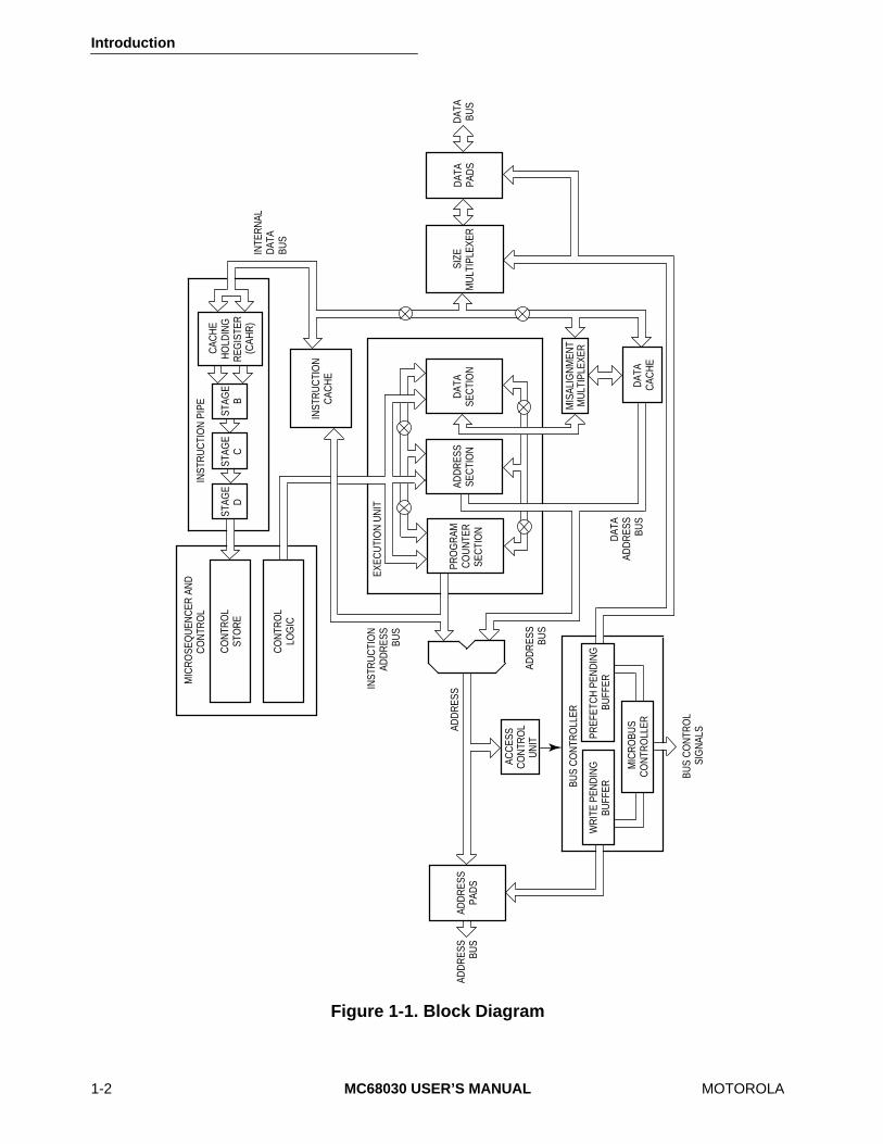
A block diagram of the MC68030 is shown in Figure 1-1. The instructions and data requiredby the processor are supplied from the internal caches whenever possible. The MMUtranslates the logical address generated by the processor into a physical address utilizingits address translation cache (ATC). The bus controller manages the transfer of databetween the CPU and memory or devices at the physical address.
Introduction
1-2
MC68030 USER’S MANUAL
MOTOROLA
Figure 1-1. Block Diagram
MIC
RO
SEQ
UEN
CER
AN
DC
ON
TRO
L
CO
NTR
OL
STO
RE
INST
RU
CTI
ON
CAC
HE
STAG
EB
STAG
EC
STAG
ED
INTE
RN
ALD
ATA
BUS
INST
RU
CTI
ON
PIP
E
INST
RU
CTI
ON
ADD
RES
SBU
S
ADD
RES
SSE
CTI
ON
PRO
GR
AMC
OU
NTE
RSE
CTI
ON
DAT
ASE
CTI
ON
EXEC
UTI
ON
UN
IT
MIS
ALIG
NM
ENT
MU
LTIP
LEXE
R
SIZE
MU
LTIP
LEXE
RD
ATA
PAD
SD
ATA
BUS
WR
ITE
PEN
DIN
GBU
FFER
PREF
ETC
H P
END
ING
BUFF
ER
MIC
RO
BUS
CO
NTR
OLL
ER
BUS
CO
NTR
OLL
ER
BUS
CO
NTR
OL
SIG
NAL
S
ADD
RES
SBU
S
ADD
RES
SPA
DS
ADD
RES
SBU
S
ADD
RES
S
DAT
AC
ACH
E
DAT
AAD
DR
ESS
BUS
CAC
HE
HO
LDIN
GR
EGIS
TER
(CAH
R)
ACC
ESS
CO
NTR
OL
UN
IT
CO
NTR
OL
LOG
IC
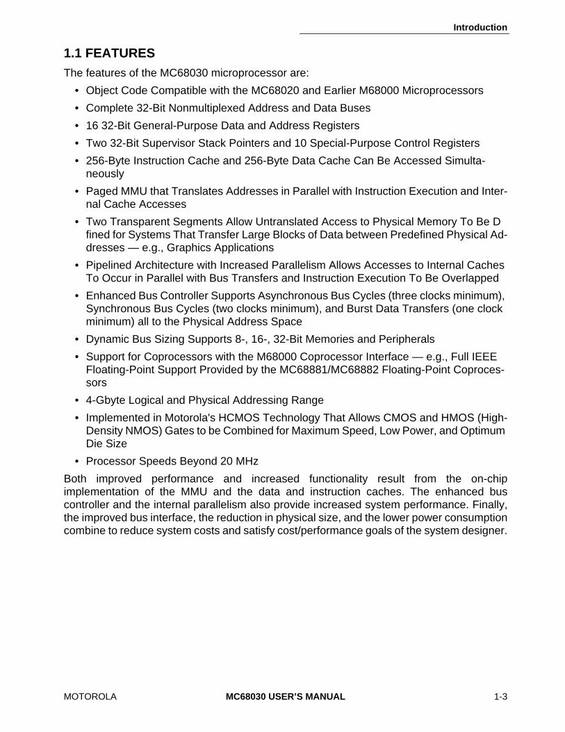
Introduction
MOTOROLA
MC68030 USER’S MANUAL
1-3
1.1 FEATURES
The features of the MC68030 microprocessor are:
• Object Code Compatible with the MC68020 and Earlier M68000 Microprocessors
• Complete 32-Bit Nonmultiplexed Address and Data Buses
• 16 32-Bit General-Purpose Data and Address Registers
• Two 32-Bit Supervisor Stack Pointers and 10 Special-Purpose Control Registers
• 256-Byte Instruction Cache and 256-Byte Data Cache Can Be Accessed Simulta-neously
• Paged MMU that Translates Addresses in Parallel with Instruction Execution and Inter-nal Cache Accesses
• Two Transparent Segments Allow Untranslated Access to Physical Memory To Be D fined for Systems That Transfer Large Blocks of Data between Predefined Physical Ad-dresses — e.g., Graphics Applications
• Pipelined Architecture with Increased Parallelism Allows Accesses to Internal Caches To Occur in Parallel with Bus Transfers and Instruction Execution To Be Overlapped
• Enhanced Bus Controller Supports Asynchronous Bus Cycles (three clocks minimum), Synchronous Bus Cycles (two clocks minimum), and Burst Data Transfers (one clock minimum) all to the Physical Address Space
• Dynamic Bus Sizing Supports 8-, 16-, 32-Bit Memories and Peripherals
• Support for Coprocessors with the M68000 Coprocessor Interface — e.g., Full IEEE Floating-Point Support Provided by the MC68881/MC68882 Floating-Point Coproces-sors
• 4-Gbyte Logical and Physical Addressing Range
• Implemented in Motorola's HCMOS Technology That Allows CMOS and HMOS (High-Density NMOS) Gates to be Combined for Maximum Speed, Low Power, and Optimum Die Size
• Processor Speeds Beyond 20 MHz
Both improved performance and increased functionality result from the on-chipimplementation of the MMU and the data and instruction caches. The enhanced buscontroller and the internal parallelism also provide increased system performance. Finally,the improved bus interface, the reduction in physical size, and the lower power consumptioncombine to reduce system costs and satisfy cost/performance goals of the system designer.

Introduction
1-4
MC68030 USER’S MANUAL
MOTOROLA
1.2 MC68030 EXTENSIONS TO THE M68000 FAMILY
In addition to the on-chip instruction cache present in the MC68020, the MC68030 has aninternal data cache. Data that is accessed during read cycles may be stored in the on-chipcache, where it is available for subsequent accesses. The data cache reduces the numberof external bus cycles when the data operand required by an instruction is already in thedata cache.
Performance is enhanced further because the on-chip caches can be internally accessed ina single clock cycle. In addition, the bus controller provides a two-clock cycle synchronousmode and burst mode accesses that can transfer data in as little as one clock per long word.
The MC68030 enhanced microprocessor contains an on-chip MMU that allows addresstranslation to operate in parallel with the CPU core, the internal caches, and the buscontroller.
Additional signals support emulation and system analysis. External debug equipment candisable the on-chip caches and the MMU to freeze the MC68030 internal state duringbreakpoint processing. In addition, the MC68030 indicates:
1. The start of a refill of the instruction pipe
2. Instruction boundaries
3. Pending trace or interrupt processing
4. Exception processing
5. Halt conditions
This status and control information allows external debugging equipment to trace theMC68030 activity and interact nonintrusively with the MC68030 to effectively reduce systemdebug effort.
1.3 PROGRAMMING MODEL
The programming model of the MC68030 consists of two groups of registers: the user modeland the supervisor model. This corresponds to the user and supervisor privilege levels. Userprograms executing at the user privilege level use the registers of the user model. Systemsoftware executing at the supervisor level uses the control registers of the supervisor levelto perform supervisor functions.
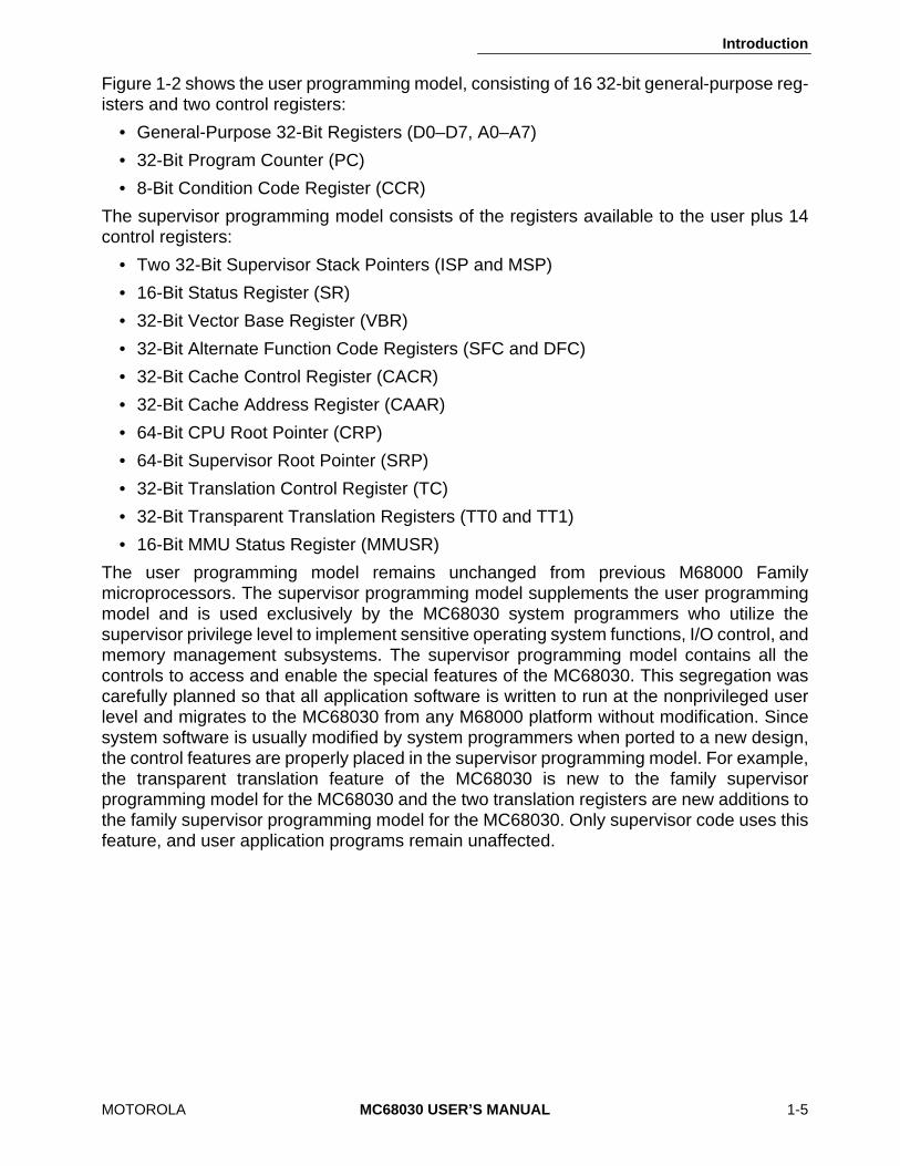
Introduction
MOTOROLA
MC68030 USER’S MANUAL
1-5
Figure 1-2 shows the user programming model, consisting of 16 32-bit general-purpose reg-isters and two control registers:
• General-Purpose 32-Bit Registers (D0–D7, A0–A7)
• 32-Bit Program Counter (PC)
• 8-Bit Condition Code Register (CCR)
The supervisor programming model consists of the registers available to the user plus 14control registers:
• Two 32-Bit Supervisor Stack Pointers (ISP and MSP)
• 16-Bit Status Register (SR)
• 32-Bit Vector Base Register (VBR)
• 32-Bit Alternate Function Code Registers (SFC and DFC)
• 32-Bit Cache Control Register (CACR)
• 32-Bit Cache Address Register (CAAR)
• 64-Bit CPU Root Pointer (CRP)
• 64-Bit Supervisor Root Pointer (SRP)
• 32-Bit Translation Control Register (TC)
• 32-Bit Transparent Translation Registers (TT0 and TT1)
• 16-Bit MMU Status Register (MMUSR)
The user programming model remains unchanged from previous M68000 Familymicroprocessors. The supervisor programming model supplements the user programmingmodel and is used exclusively by the MC68030 system programmers who utilize thesupervisor privilege level to implement sensitive operating system functions, I/O control, andmemory management subsystems. The supervisor programming model contains all thecontrols to access and enable the special features of the MC68030. This segregation wascarefully planned so that all application software is written to run at the nonprivileged userlevel and migrates to the MC68030 from any M68000 platform without modification. Sincesystem software is usually modified by system programmers when ported to a new design,the control features are properly placed in the supervisor programming model. For example,the transparent translation feature of the MC68030 is new to the family supervisorprogramming model for the MC68030 and the two translation registers are new additions tothe family supervisor programming model for the MC68030. Only supervisor code uses thisfeature, and user application programs remain unaffected.
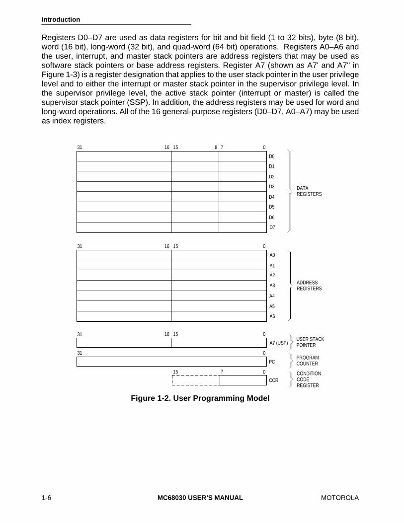
Introduction
1-6
MC68030 USER’S MANUAL
MOTOROLA
Registers D0–D7 are used as data registers for bit and bit field (1 to 32 bits), byte (8 bit),word (16 bit), long-word (32 bit), and quad-word (64 bit) operations. Registers A0–A6 andthe user, interrupt, and master stack pointers are address registers that may be used assoftware stack pointers or base address registers. Register A7 (shown as A7' and A7'' inFigure 1-3) is a register designation that applies to the user stack pointer in the user privilegelevel and to either the interrupt or master stack pointer in the supervisor privilege level. Inthe supervisor privilege level, the active stack pointer (interrupt or master) is called thesupervisor stack pointer (SSP). In addition, the address registers may be used for word andlong-word operations. All of the 16 general-purpose registers (D0–D7, A0–A7) may be usedas index registers.
Figure 1-2. User Programming Model
31 16 15 8 7
7
0
31 16 15 0
31 16 15
15
0
31 0
0
CCR
PC
A7 (USP)
D0
D1
D2
D3
D4
D5
D6
D7
A0
A1
A2
A3
A4
A5
A6
DATAREGISTERS
ADDRESSREGISTERS
USER STACKPOINTER
PROGRAMCOUNTER
CONDITIONCODEREGISTER
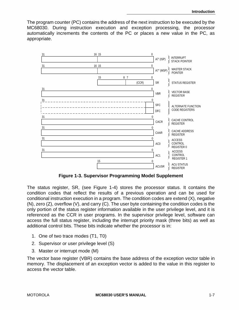
Introduction
MOTOROLA
MC68030 USER’S MANUAL
1-7
The program counter (PC) contains the address of the next instruction to be executed by theMC68030. During instruction execution and exception processing, the processorautomatically increments the contents of the PC or places a new value in the PC, asappropriate.
The status register, SR, (see Figure 1-4) stores the processor status. It contains thecondition codes that reflect the results of a previous operation and can be used forconditional instruction execution in a program. The condition codes are extend (X), negative(N), zero (Z), overflow (V), and carry (C). The user byte containing the condition codes is theonly portion of the status register information available in the user privilege level, and it isreferenced as the CCR in user programs. In the supervisor privilege level, software canaccess the full status register, including the interrupt priority mask (three bits) as well asadditional control bits. These bits indicate whether the processor is in:
1. One of two trace modes (T1, T0)
2. Supervisor or user privilege level (S)
3. Master or interrupt mode (M)
The vector base register (VBR) contains the base address of the exception vector table inmemory. The displacement of an exception vector is added to the value in this register toaccess the vector table.
Figure 1-3. Supervisor Programming Model Supplement
31 16 15 0
31 16 15 0
15 8 7 0
(CCR) SR
A7" (MSP)
A7' (ISP)
31 0
VBR
SFC
DFC
CACR
CAAR
INTERRUPTSTACK POINTER
MASTER STACKPOINTER
STATUS REGISTER
VECTOR BASEREGISTER
ALTERNATE FUNCTIONCODE REGISTERS
CACHE CONTROLREGISTER
CACHE ADDRESSREGISTER
0
0
0
31
31
31
AC0ACCESSCONTROLREGISTER 0
031
AC1ACCESSCONTROLREGISTER 1
031
ACUSRACU STATUSREGISTER
015

Introduction
1-8
MC68030 USER’S MANUAL
MOTOROLA
Alternate function code registers, SFC and DFC, contain 3-bit function codes. Functioncodes can be considered extensions of the 32-bit linear address that optionally provide asmany as eight 4-Gbyte address spaces. Function codes are automatically generated by theprocessor to select address spaces for data and program at the user and supervisorprivilege levels and a CPU address space for processor functions (e.g., coprocessorcommunications). Registers SFC and DFC are used by certain instructions to explicitlyspecify the function codes for operations.
The cache control register (CACR) controls the on-chip instruction and data caches of theMC68030. The cache address register (CAAR) stores an address for cache controlfunctions.
The CPU root pointer (CRP) contains a pointer to the root of the translation tree for thecurrently executing task of the MC68030. This tree contains the mapping information for thetask's address space. When the MC68030 is configured to provide a separate addressspace for supervisor routines, the supervisor root pointer (SRP) contains a pointer to the rootof the translation tree describing the supervisor's address space.
The translation control register (TC) consists of several fields that control addresstranslation. These fields enable and disable address translation, enable and disable the useof SRP for the supervisor address space, and select or ignore the function codes intranslating addresses. Other fields define the size of memory pages, the number of addressbits used in translation, and the translation table structure.
The transparent translation registers, TT0 and TT1, can each specify separate blocks ofmemory as directly accessible without address translation. Logical addresses in these areasbecome the physical addresses for memory access. Function codes and the eight mostsignificant bits of the address can be used to define the area of memory and type of access;either read, write, or both types of memory access can be directly mapped. The transparenttranslation feature allows rapid movement of large blocks of data in memory or I/O spacewithout disturbing the context of the on-chip address translation cache or incurring delaysassociated with translation table lookups. This feature is useful to graphics, controller, andreal-time applications.
Figure 1-4. Status Register
T1 T0 S M 0 I2 I1 I0 X N Z V C0 0 0
SYSTEM BYTEUSER BYTE
(CONDITION CODE REGISTER)
TRACEENABLE
INTERRUPTPRIORITY MASK
SUPERVISOR/USERSTATE
MASTER/INTERRUPTSTATE EXTEND
NEGATIVE
ZERO
OVERFLOW
CARRY
15 14 13 12 11 10 9 8 7 56 4 3 2 1 0

Introduction
MOTOROLA
MC68030 USER’S MANUAL
1-9
The MMU status register (MMUSR) contains memory management status informationresulting from a search of the address translation cache or the translation tree for a particularlogical address.
1.4 DATA TYPES AND ADDRESSING MODES
Seven basic data types are supported:
1. Bits
2. Bit Fields (Fields of consecutive bits, 1–32 bits long)
3. BCD Digits (Packed: 2 digits/byte, Unpacked: 1 digit/byte)
4. Byte Integers (8 bits)
5. Word Integers (16 bits)
6. Long-Word Integers (32 bits)
7. Quad-Word Integers (64 bits)
In addition, the instruction set supports operations on other data types such as memoryaddresses. The coprocessor mechanism allows direct support of floating-point operationswith the MC68881 and MC68882 floating-point coprocessors as well as specialized user-defined data types and functions.
The 18 addressing modes, shown in Table 1-1, include nine basic types:
1. Register Direct
2. Register Indirect
3. Register Indirect with Index
4. Memory Indirect
5. Program Counter Indirect with Displacement
6. Program Counter Indirect with Index
7. Program Counter Memory Indirect
8. Absolute
9. Immediate
The register indirect addressing modes can also postincrement, predecrement, offset, andindex addresses. The program counter relative mode also has index and offset capabilities.As in the MC68020, both modes are extended to provide indirect reference through memory.In addition to these addressing modes, many instructions implicitly specify the use of thecondition code register, stack pointer, and/or program counter.
1.5 INSTRUCTION SET OVERVIEW
The instructions in the MC68030 instruction set are listed in Table 1-2. The instruction sethas been tailored to support structured high-level languages and sophisticated operatingsystems. Many instructions operate on bytes, words, or long words, and most instructionscan use any of the 18 addressing modes.

Introduction
1-10
MC68030 USER’S MANUAL
MOTOROLA
NOTES:Dn = Data Register, D0–D7An = Address Register, A0–A7
8,
d
16 = A twos-complement or sign-extended displacement; added as part of the effective address calculation; size is 8 (d
8
) or 16 (d
16
) bits; when omitted, assemblers use a value of zero.Xn = Address or data register used as an index register; form is Xn.SIZE*SCALE, where SIZE is .W
or .L indicates index register size) and SCALE is 1, 2, 4, or 8 (index register is multiplied by SCALE); use of SIZE and/or SCALE is optional.
bd = A twos-complement base displacement;when present, size can be 16 or 32 bits.od = Outer displacement, added as part of effective address calculation after any memory
indirection; use is optional with asize of 16 or 32 bits.PC = Program Counter
(data) = Immediate value of 8, 16, or 32 bits( ) = Effective Address[ ] = Use as indirect access to long-word address.
Table 1-1. Addressing Modes
Addressing Modes Syntax
Register DirectData Register DirectAddress Register Direct
DnAn
Register IndirectAddress Register IndirectAddress Register Indirect with PostincrementAddress Register Indirect with PredecrementAddress Register Indirect with Displacement
(An)(An)–(An)(d
16
,An)
Register Indirect with IndexAddress Register Indirect with Index (8-BitDisplacement)Address Register Indirect with Index (Base Displacement)
(d
8
,An,Xn)(bd,An,Xn)
Memory IndirectMemory Indirect PostindexedMemory Indirect Preindexed
([bd,An],Xn,od)([bd,An,Xn],od)
Program Counter Indirect with Displacement (d
16
,PC)
Program Cou nter Indirect with IndexPC Indirect with Index (8-Bit Displacement)PC Indirect with Index (Base Displacement)
(d
8
,PC,Xn)(bd,PC,Xn)
Program Counter Memory IndirectPC Memory Indirect PostindexedPC Memory Indirect Preindexed
([bd,PC],Xn,od)([bd,PC,Xn],od)
AbsoluteAbsolute ShortAbsolute Long
(xxx).W(xxx).L
Immediate #(data)

Introduction
MOTOROLA
MC68030 USER’S MANUAL
1-11
1.6 VIRTUAL MEMORY AND VIRTUAL MACHINE CONCEPTS
The full addressing range of the MC68030 is 4 Gbytes (4,294,967,296 bytes) in each of eightaddress spaces. Even though most systems implement a smaller physical memory, thesystem can be made to appear to have a full 4 Gbytes of memory available to each userprogram by using virtual memory techniques.
In a virtual memory system, a user program can be written as if it has a large amount ofmemory available, when the physical memory actually present is much smaller. Similarly, asystem can be designed to allow user programs to access devices that are not physicallypresent in the system, such as tape drives, disk drives, printers, terminals, and so forth. Withproper software emulation, a physical system can appear to be any other M68000 computersystem to a user program, and the program can be given full access to all of the resourcesof that emulated system. Such an emulated system is called a virtual machine.
1.6.1 Virtual Memory
A system that supports virtual memory has a limited amount of high-speed physical memorythat can be accessed directly by the processor and maintains an image of a much largervirtual memory on a secondary storage device such as a large-capacity disk drive. Whenthe processor attempts to access a location in the virtual memory map that is not resident inphysical memory, a page fault occurs. The access to that location is temporarily suspendedwhile the necessary data is fetched from secondary storage and placed in physical memory.The suspended access is then either restarted or continued.
The MC68030 uses instruction continuation to support virtual memory. When a bus cycle isterminated with a bus error, the microprocessor suspends the current instruction andexecutes the virtual memory bus error handler. When the bus error handler has completedexecution, it returns control to the program that was executing when the error was detected,reruns the faulted bus cycle (when required), and continues the suspended instruction.
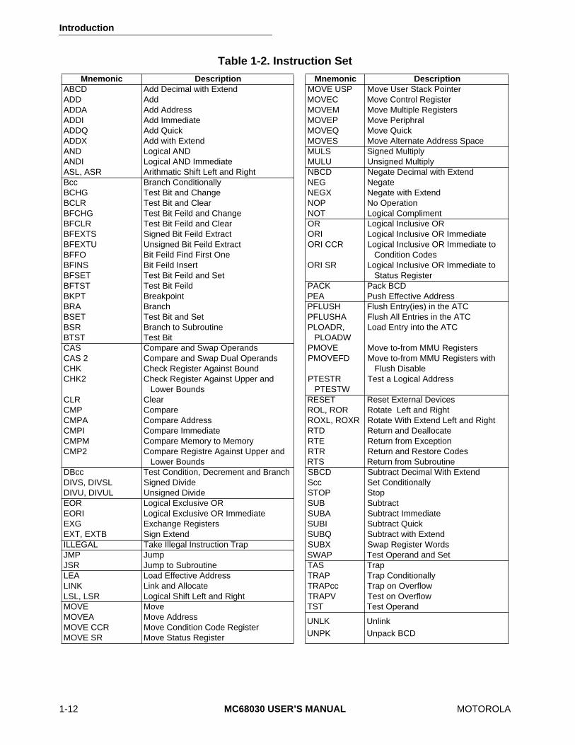
Introduction
1-12
MC68030 USER’S MANUAL
MOTOROLA
Table 1-2. Instruction Set
Mnemonic Description Mnemonic Description
ABCD Add Decimal with Extend MOVE USP Move User Stack PointerADD Add MOVEC Move Control RegisterADDA Add Address MOVEM Move Multiple RegistersADDI Add Immediate MOVEP Move PeriphralADDQ Add Quick MOVEQ Move QuickADDX Add with Extend MOVES Move Alternate Address SpaceAND Logical AND MULS Signed MultiplyANDI Logical AND Immediate MULU Unsigned MultiplyASL, ASR Arithmatic Shift Left and Right NBCD Negate Decimal with ExtendBcc Branch Conditionally NEG NegateBCHG Test Bit and Change NEGX Negate with Extend BCLR Test Bit and Clear NOP No OperationBFCHG Test Bit Feild and Change NOT Logical ComplimentBFCLR Test Bit Feild and Clear OR Logical Inclusive ORBFEXTS Signed Bit Feild Extract ORI Logical Inclusive OR ImmediateBFEXTU Unsigned Bit Feild Extract ORI CCR Logical Inclusive OR Immediate toBFFO Bit Feild Find First One Condition CodesBFINS Bit Feild Insert ORI SR Logical Inclusive OR Immediate toBFSET Test Bit Feild and Set Status RegisterBFTST Test Bit Feild PACK Pack BCDBKPT Breakpoint PEA Push Effective AddressBRA Branch PFLUSH Flush Entry(ies) in the ATCBSET Test Bit and Set PFLUSHA Flush All Entries in the ATCBSR Branch to Subroutine PLOADR, Load Entry into the ATCBTST Test Bit PLOADWCAS Compare and Swap Operands PMOVE Move to-from MMU RegistersCAS 2 Compare and Swap Dual Operands PMOVEFD Move to-from MMU Registers withCHK Check Register Against Bound Flush DisableCHK2 Check Register Against Upper and PTESTR Test a Logical Address
Lower Bounds PTESTWCLR Clear RESET Reset External Devices CMP Compare ROL, ROR Rotate Left and RightCMPA Compare Address ROXL, ROXR Rotate With Extend Left and RightCMPI Compare Immediate RTD Return and Deallocate CMPM Compare Memory to Memory RTE Return from ExceptionCMP2 Compare Registre Against Upper and RTR Return and Restore Codes
Lower Bounds RTS Return from SubroutineDBcc Test Condition, Decrement and Branch SBCD Subtract Decimal With ExtendDIVS, DIVSL Signed Divide Scc Set ConditionallyDIVU, DIVUL Unsigned Divide STOP StopEOR Logical Exclusive OR SUB Subtract EORI Logical Exclusive OR Immediate SUBA Subtract Immediate EXG Exchange Registers SUBI Subtract QuickEXT, EXTB Sign Extend SUBQ Subtract with Extend ILLEGAL Take Illegal Instruction Trap SUBX Swap Register WordsJMP Jump SWAP Test Operand and SetJSR Jump to Subroutine TAS Trap LEA Load Effective Address TRAP Trap ConditionallyLINK Link and Allocate TRAPcc Trap on OverflowLSL, LSR Logical Shift Left and Right TRAPV Test on OverflowMOVE Move TST Test Operand MOVEA Move Address UNLK
UNPKUnlinkUnpack BCD
MOVE CCR Move Condition Code RegisterMOVE SR Move Status Register
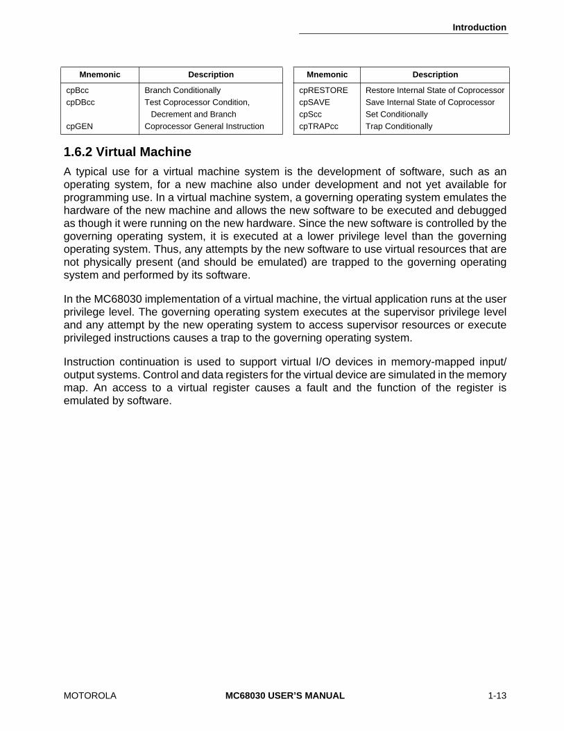
Introduction
MOTOROLA
MC68030 USER’S MANUAL
1-13
1.6.2 Virtual Machine
A typical use for a virtual machine system is the development of software, such as anoperating system, for a new machine also under development and not yet available forprogramming use. In a virtual machine system, a governing operating system emulates thehardware of the new machine and allows the new software to be executed and debuggedas though it were running on the new hardware. Since the new software is controlled by thegoverning operating system, it is executed at a lower privilege level than the governingoperating system. Thus, any attempts by the new software to use virtual resources that arenot physically present (and should be emulated) are trapped to the governing operatingsystem and performed by its software.
In the MC68030 implementation of a virtual machine, the virtual application runs at the userprivilege level. The governing operating system executes at the supervisor privilege leveland any attempt by the new operating system to access supervisor resources or executeprivileged instructions causes a trap to the governing operating system.
Instruction continuation is used to support virtual I/O devices in memory-mapped input/output systems. Control and data registers for the virtual device are simulated in the memorymap. An access to a virtual register causes a fault and the function of the register isemulated by software.
Mnemonic Description Mnemonic Description
cpBcccpDBcc
cpGEN
Branch ConditionallyTest Coprocessor Condition,
Decrement and BranchCoprocessor General Instruction
cpRESTOREcpSAVEcpScccpTRAPcc
Restore Internal State of CoprocessorSave Internal State of CoprocessorSet ConditionallyTrap Conditionally
Introduction
1-14
MC68030 USER’S MANUAL
MOTOROLA
1.7 THE MEMORY MANAGEMENT UNIT
The MMU supports virtual memory systems by translating logical addresses to physical ad-dresses using translation tables stored in memory. The MMU stores address mappings inan address translation cache (ATC) that contains the most recently used translations. Whenthe ATC contains the address for a bus cycle requested by the CPU, a translation tablesearch is not performed. Features of the MMU include:
• Multiple Level Translation Tables with Short- and Long-Format Descriptors for Efficient Table Space Usage
• Table Searches Automatically Performed in Microcode
• 22-Entry Fully Associative ATC
• Address Translations and Internal Instruction and Data Cache Accesses Performed in Parallel
• Eight Page Sizes Available Ranging from 256 to 32K Bytes
• Two Optional Transparent Blocks
• User and Supervisor Root Pointer Registers
• Write Protection and Supervisor Protection Attributes
• Translations Enabled/Disabled by Software
• Translations Can Be Disabled with External MMUDIS Signal
• Used and Modified Bits Automatically Maintained in Tables and ATC
• Cache Inhibit Output (CIOUT) Signal Can Be Asserted on a Page-by-Page Basis
• 32-Bit Internal Logical Address with Capability To Ignore as many as 15 Upper Address Bits
• 3-Bit Function Code Supports Separate Address Spaces
• 32-Bit Physical Address
The memory management function performed by the MMU is called demand paged memorymanagement. Since a task specifies the areas of memory it requires as it executes, memoryallocation is supported on a demand basis. If a requested access to memory is not currentlymapped by the system, then the access causes a demand for the operating system to loador allocate the required memory image. The technique used by the MC68030 is pagedmemory management because physical memory is managed in blocks of a specifiednumber of bytes, called page frames. The logical address space is divided into fixed-sizepages that contain the same number of bytes as the page frames. Memory managementassigns a physical base address to a logical page. The system software then transfers databetween secondary storage and memory one or more pages at a time.
Introduction
MOTOROLA
MC68030 USER’S MANUAL
1-15
1.8 PIPELINED ARCHITECTURE
The MC68030 uses a three-stage pipelined internal architecture to provide for optimuminstruction throughput. The pipeline allows as many as three words of a single instruction orthree consecutive instructions to be decoded concurrently.
1.9 THE CACHE MEMORIES
Due to locality of reference, instructions and data that are used in a program have a highprobability of being reused within a short time. Additionally, instructions and data operandsthat reside in proximity to the instructions and data currently in use also have a highprobability of being utilized within a short period. To exploit these locality characteristics, theMC68030 contains two on-chip logical caches, a data cache, and an instruction cache.
Each of the caches stores 256 bytes of information, organized as 16 entries, each containinga block of four long words (16 bytes). The processor fills the cache entries either one longword at a time or, during burst mode accesses, four long words consecutively. The burstmode of operation not only fills the cache efficiently but also captures adjacent instruction ordata items that are likely to be required in the near future due to locality characteristics ofthe executing task.
The caches improve the overall performance of the system by reducing the number of buscycles required by the processor to fetch information from memory and by increasing thebus bandwidth available for other bus masters in the system. Addition of the data cache inthe MC68030 extends the benefits of cache techniques to all memory accesses. During awrite cycle, the data cache circuitry writes data to a cached data item as well as to the itemin memory, maintaining consistency between data in the cache and that in memory.However, writing data that is not in the cache may or may not cause the data item to bestored in the cache, depending on the write allocation policy selected in the cache controlregister (CACR).
MOTOROLA
MC68030 USER’S MANUAL
2-1
SECTION 2DATA ORGANIZATION AND ADDRESSING CAPABILITIES
Most external references to memory by a microprocessor are either program references ordata references; they either access instruction words or operands (data items) for aninstruction. Program references are references to the program space, the section of memorythat contains the program instructions and any immediate data operands that reside in theinstruction stream. Refer to M68000PM/AD,
M68000 Programmer's Reference Manual
, fordescriptions of the instructions in the program space. Data references refer to the dataspace, the section of memory that contains the program data. Data items in the instructionstream can be accessed with the program counter relative addressing modes, and theseaccesses are classified as program references. A third type of external reference used forcoprocessor communications, interrupt acknowledge cycles, and breakpoint acknowledgecycles is classified as a CPU space reference. The MC68030 automatically sets the functioncodes to access the program space, the data space, or the CPU space for special functionsas required. The function codes can be used by the memory management unit to organizeseparate program (read only) and data (read-write) memory areas.
This section describes the data organization and addressing capabilities of the MC68030. Itlists the types of operands used by instructions and describes the registers and their use asoperands. Next, the section describes the organization of data in memory and theaddressing modes available to access data in memory. Last, the section describes thesystem stack and user program stacks and queues.
2.1 INSTRUCTION OPERANDS
The MC68030 supports a general-purpose set of operands to serve the requirements of alarge range of applications. Operands of MC68030 instructions may reside in registers, inmemory, or within the instructions themselves. An instruction operand might also reside ina coprocessor. An operand may be a single bit, a bit field of from 1 to 32 bits in length, a byte(8 bits), a word (16 bits), a long word (32 bits), or a quad word (64 bits). The operand sizefor each instruction is either explicitly encoded in the instruction or implicitly defined by theinstruction operation. Coprocessors are designed to support special computation modelsthat require very specific but widely varying data operand types and sizes. Hence,coprocessor instructions can specify operands of any size.

Data Organization and Addressing Capabilities
2-2
MC68030 USER’S MANUAL
MOTOROLA
2.2 ORGANIZATION OF DATA IN REGISTERS
The eight data registers can store data operands of 1, 8, 16, 32, and 64 bits, addresses of16 or 32 bits, or bit fields of 1 to 32 bits. The seven address registers and the three stackpointers are used for address operands of 16 or 32 bits. The control registers (SR, VBR,SFC, DFC, CACR, CAAR, CRP, SRP, TC, TT0, TT1, and MMUSR) vary in size accordingto function. Coprocessors may define unique operand sizes and support them with on-chipregisters accordingly.
2.2.1 Data Registers
Each data register is 32 bits wide. Byte operands occupy the low-order 8 bits, wordoperands the low-order 16 bits, and long-word operands the entire 32 bits. When a dataregister is used as either a source or destination operand, only the appropriate low-orderbyte or word (in byte or word operations, respectively) is used or changed; the remaininghigh-order portion is neither used nor changed. The least significant bit of a long-wordinteger is addressed as bit zero, and the most significant bit is addressed as bit 31. For bitfields, the most significant bit is addressed as bit zero, and the least significant bit isaddressed as the width of the field minus one. If the width of the field plus the offset is greaterthan 32, the bit field wraps around within the register. The following illustration shows theorganization of various types of data in the data registers.
Quad-word data consists of two long words; for example, the product of 32-bit multiply orthe quotient of 32-bit divide operations (signed and unsigned). Quad words may beorganized in any two data registers without restrictions on order or pairing. There are noexplicit instructions for the managment of this data type, although the MOVEM instructioncan be used to move a quad word into or out of the registers.
Binary-coded decimal (BCD) data represents decimal numbers in binary form. Althoughmany BCD codes have been devised, the BCD instructions of the M68000 Family supportformats which the four least significant bits consist of a binary number having the numericvalue of the corresponding decimal number. Two BCD formats are used. In the unpackedBCD format, a byte contains one digit; the four least significant bits contain the binary valueand the four most significant bits are undefined. Each byte of the packed BCD formatcontains two digits; the least significant four bits contain the least significant digit.
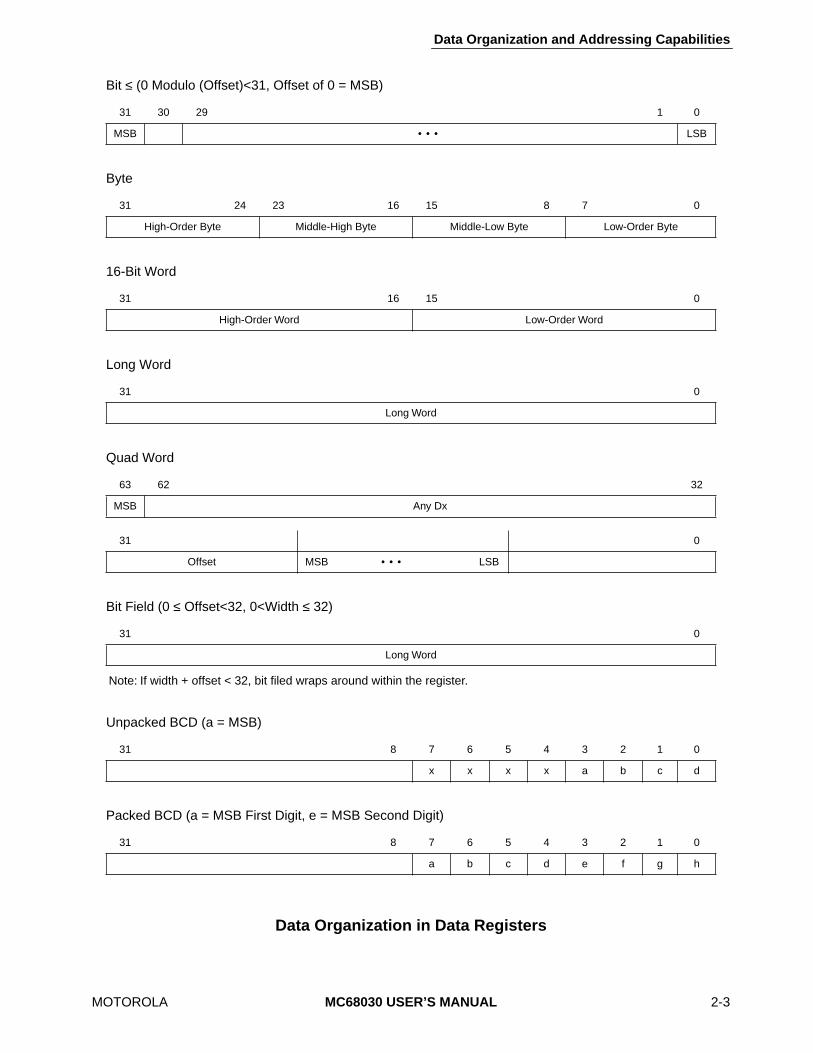
Data Organization and Addressing Capabilities
MOTOROLA
MC68030 USER’S MANUAL
2-3
Note: If width + offset < 32, bit filed wraps around within the register.
Data Organization in Data Registers
Bit
≤
(0 Modulo (Offset)<31, Offset of 0 = MSB)
31 30 29 1 0
MSB
• • •
LSB
Byte
31 24 23 16 15 8 7 0
High-Order Byte Middle-High Byte Middle-Low Byte Low-Order Byte
16-Bit Word
31 16 15 0
High-Order Word Low-Order Word
Long Word
31 0
Long Word
Quad Word
63 62 32
MSB Any Dx
31 0
Offset MSB
• • •
LSB
Bit Field (0
≤
Offset<32, 0<Width
≤
32)
31 0
Long Word
Unpacked BCD (a = MSB)
31 8 7 6 5 4 3 2 1 0
x x x x a b c d
Packed BCD (a = MSB First Digit, e = MSB Second Digit)
31 8 7 6 5 4 3 2 1 0
a b c d e f g h
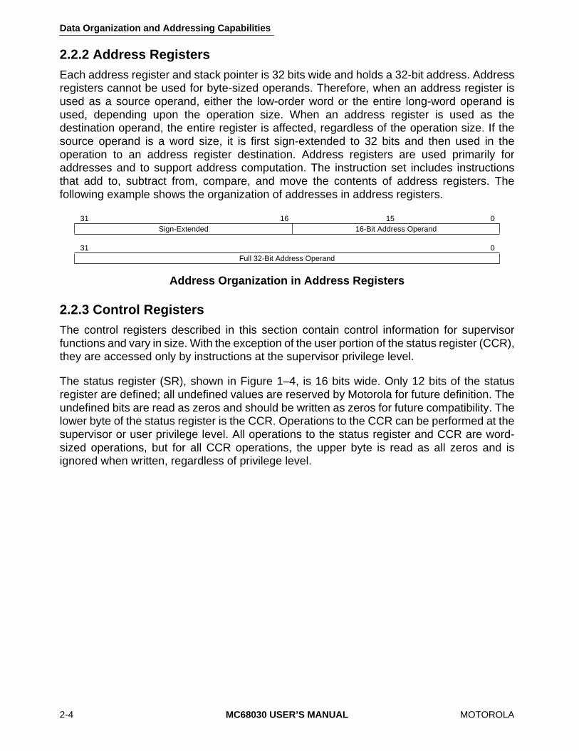
Data Organization and Addressing Capabilities
2-4
MC68030 USER’S MANUAL
MOTOROLA
2.2.2 Address Registers
Each address register and stack pointer is 32 bits wide and holds a 32-bit address. Addressregisters cannot be used for byte-sized operands. Therefore, when an address register isused as a source operand, either the low-order word or the entire long-word operand isused, depending upon the operation size. When an address register is used as thedestination operand, the entire register is affected, regardless of the operation size. If thesource operand is a word size, it is first sign-extended to 32 bits and then used in theoperation to an address register destination. Address registers are used primarily foraddresses and to support address computation. The instruction set includes instructionsthat add to, subtract from, compare, and move the contents of address registers. Thefollowing example shows the organization of addresses in address registers.
Address Organization in Address Registers
2.2.3 Control Registers
The control registers described in this section contain control information for supervisorfunctions and vary in size. With the exception of the user portion of the status register (CCR),they are accessed only by instructions at the supervisor privilege level.
The status register (SR), shown in Figure 1–4, is 16 bits wide. Only 12 bits of the statusregister are defined; all undefined values are reserved by Motorola for future definition. Theundefined bits are read as zeros and should be written as zeros for future compatibility. Thelower byte of the status register is the CCR. Operations to the CCR can be performed at thesupervisor or user privilege level. All operations to the status register and CCR are word-sized operations, but for all CCR operations, the upper byte is read as all zeros and isignored when written, regardless of privilege level.
31 16 15 0 Sign-Extended 16-Bit Address Operand
31 0Full 32-Bit Address Operand

Data Organization and Addressing Capabilities
MOTOROLA
MC68030 USER’S MANUAL
2-5
The supervisor programming model (see Figure 1–3) shows the control registers. The cachecontrol register (CACR) provides control and status information for the on-chip instructionand data caches. The cache address register (CAAR) contains the address for cache controlfunctions. The vector base register (VBR) provides the base address of the exception vectortable. All operations involving the CACR, CAAR, and VBR are long-word operations,whether these registers are used as the source or the destination operand.
The alternate function code registers (SFC and DFC)
are 32-bit registers with only bits 2:0 implemented that contain the address space values(FC0-FC2) for the read or write operands of MOVES, PLOAD, PFLUSH, and PTESTinstructions. The MOVEC instruction is used to transfer values to and from the alternatefunction code registers. These are long-word transfers; the upper 29 bits are read as zerosand are ignored when written.
The remaining control registers in the supervisor programming model are used by thememory management unit (MMU). The CPU root pointer (CRP) and supervisor root pointer(SRP) contain pointers to the user and supervisor address translation trees. Transfers ofdata to and from these 64-bit registers are quad-word transfers. The translation controlregister (TC) contains control information for the MMU. The MC68030 always uses long-word transfers to access this 32-bit register. The transparent translation registers (TT0 andTT1) also contain 32 bits each; they identify memory areas for direct addressing withoutaddress translation. Data transfers to and from these registers are long-word transfers. TheMMU status register (MMUSR) stores the status of the MMU after execution of a PTESTinstruction. It is a 16-bit register, and transfers to and from the MMUSR are word transfers.Refer to
Section 9 Memory Management Unit
for more detail.
2.3 ORGANIZATION OF DATA IN MEMORY
Memory is organized on a byte-addressable basis where lower addresses correspond tohigher order bytes. The address, N, of a long-word data item corresponds to the address ofthe most significant byte of the highest order word. The lower order word is located ataddress N + 2, leaving the least significant byte at address N + 3 (refer to Figure 2–1). Noticethat the MC68030 does not require data to be aligned on word boundaries (refer to Figure2–2), but the most efficient data transfers occur when data is aligned on the same byteboundary as its operand size. However, instruction words must be aligned on wordboundaries.
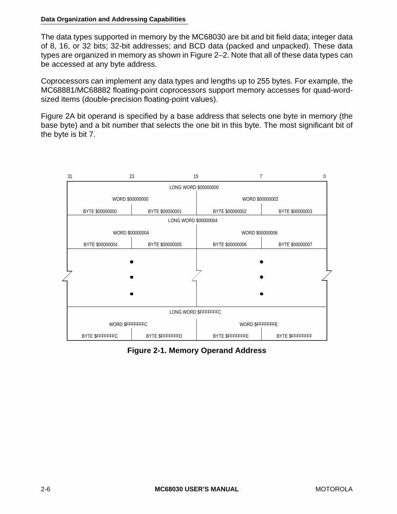
Data Organization and Addressing Capabilities
2-6
MC68030 USER’S MANUAL
MOTOROLA
The data types supported in memory by the MC68030 are bit and bit field data; integer dataof 8, 16, or 32 bits; 32-bit addresses; and BCD data (packed and unpacked). These datatypes are organized in memory as shown in Figure 2–2. Note that all of these data types canbe accessed at any byte address.
Coprocessors can implement any data types and lengths up to 255 bytes. For example, theMC68881/MC68882 floating-point coprocessors support memory accesses for quad-word-sized items (double-precision floating-point values).
Figure 2A bit operand is specified by a base address that selects one byte in memory (thebase byte) and a bit number that selects the one bit in this byte. The most significant bit ofthe byte is bit 7.
Figure 2-1. Memory Operand Address
31 23 15 7 0
BYTE $00000000
WORD $00000000
LONG WORD $00000000
BYTE $00000001 BYTE $00000002 BYTE $00000003
WORD $00000002
BYTE $00000004
WORD $00000004
LONG WORD $00000004
BYTE $00000005 BYTE $00000006 BYTE $00000007
WORD $00000006
BYTE $FFFFFFFC
WORD $FFFFFFFC
LONG WORD $FFFFFFFC
BYTE $FFFFFFFD BYTE $FFFFFFFE BYTE $FFFFFFFF
WORD $FFFFFFFE
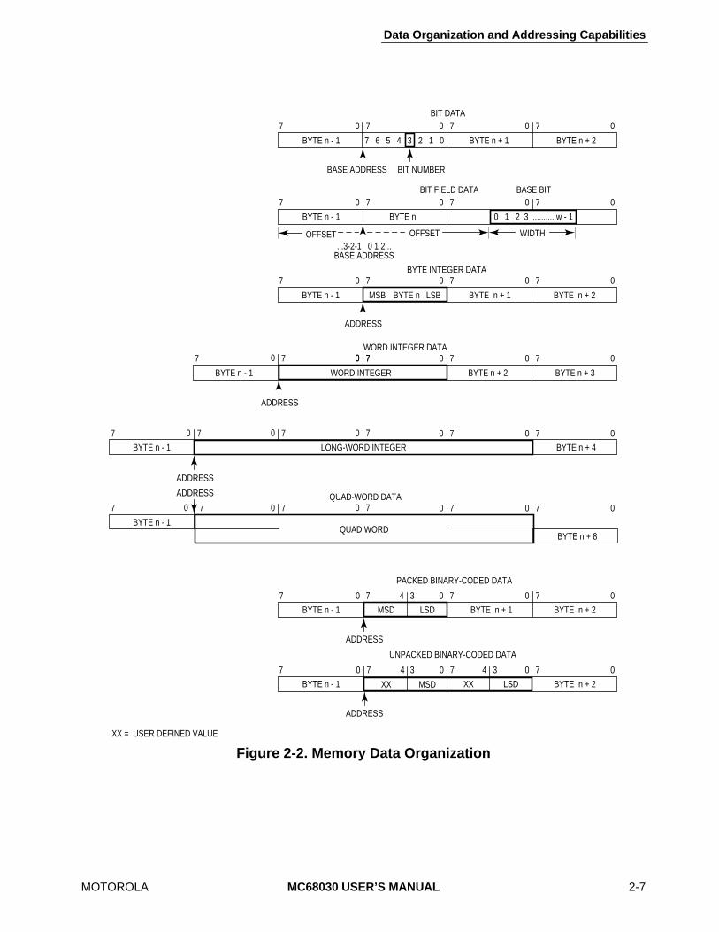
Data Organization and Addressing Capabilities
MOTOROLA
MC68030 USER’S MANUAL
2-7
Figure 2-2. Memory Data Organization
0 77 0 7 0 7 0
0 77 0 7 0 7 0
0 77 0 7 0 7 0
0 77 0 7 0 7 0
0 77 0 7 0 7 0
0 7 0 7 0 7 0
BYTE n - 1 BYTE n + 17 6 5 4 3 2 1 0 BYTE n + 2
BASE ADDRESS BIT NUMBER
BIT DATA
BYTE n - 1
BIT FIELD DATA BASE BIT
BYTE n 0 1 2 3 ...........w - 1
WIDTHOFFSETOFFSET ...3-2-1 0 1 2...BASE ADDRESS
BYTE n - 1 BYTE n + 2
BYTE INTEGER DATA
BYTE n + 1MSB BYTE n LSB
ADDRESS
WORD INTEGER BYTE n + 2 BYTE n + 3
ADDRESS
WORD INTEGER DATA7077 0
70 0 7 0 7 07077 0
LONG-WORD INTEGER BYTE n + 4
70 0 7 0 7 07077 0
ADDRESS
BYTE n - 1
QUAD WORDBYTE n + 8
BYTE n - 1
QUAD-WORD DATA
BYTE n - 1 BYTE n + 2BYTE n + 1MSD LSD
ADDRESS
PACKED BINARY-CODED DATA
4 3
BYTE n - 1 BYTE n + 2XX MSD
ADDRESS
4 3
XX LSD
4 3
XX = USER DEFINED VALUE
ADDRESS
UNPACKED BINARY-CODED DATA
BYTE n - 1
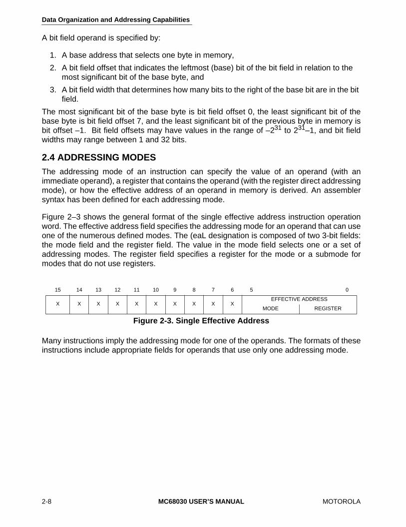
Data Organization and Addressing Capabilities
2-8
MC68030 USER’S MANUAL
MOTOROLA
A bit field operand is specified by:
1. A base address that selects one byte in memory,
2. A bit field offset that indicates the leftmost (base) bit of the bit field in relation to the most significant bit of the base byte, and
3. A bit field width that determines how many bits to the right of the base bit are in the bit field.
The most significant bit of the base byte is bit field offset 0, the least significant bit of thebase byte is bit field offset 7, and the least significant bit of the previous byte in memory isbit offset –1. Bit field offsets may have values in the range of –2
31
to 2
31
–1, and bit fieldwidths may range between 1 and 32 bits.
2.4 ADDRESSING MODES
The addressing mode of an instruction can specify the value of an operand (with animmediate operand), a register that contains the operand (with the register direct addressingmode), or how the effective address of an operand in memory is derived. An assemblersyntax has been defined for each addressing mode.
Figure 2–3 shows the general format of the single effective address instruction operationword. The effective address field specifies the addressing mode for an operand that can useone of the numerous defined modes. The (eaL designation is composed of two 3-bit fields:the mode field and the register field. The value in the mode field selects one or a set ofaddressing modes. The register field specifies a register for the mode or a submode formodes that do not use registers.
Figure 2-3. Single Effective Address
Many instructions imply the addressing mode for one of the operands. The formats of theseinstructions include appropriate fields for operands that use only one addressing mode.
15 14 13 12 11 10 9 8 7 6 5 0
X X X X X X X X X XEFFECTIVE ADDRESS
MODE REGISTER
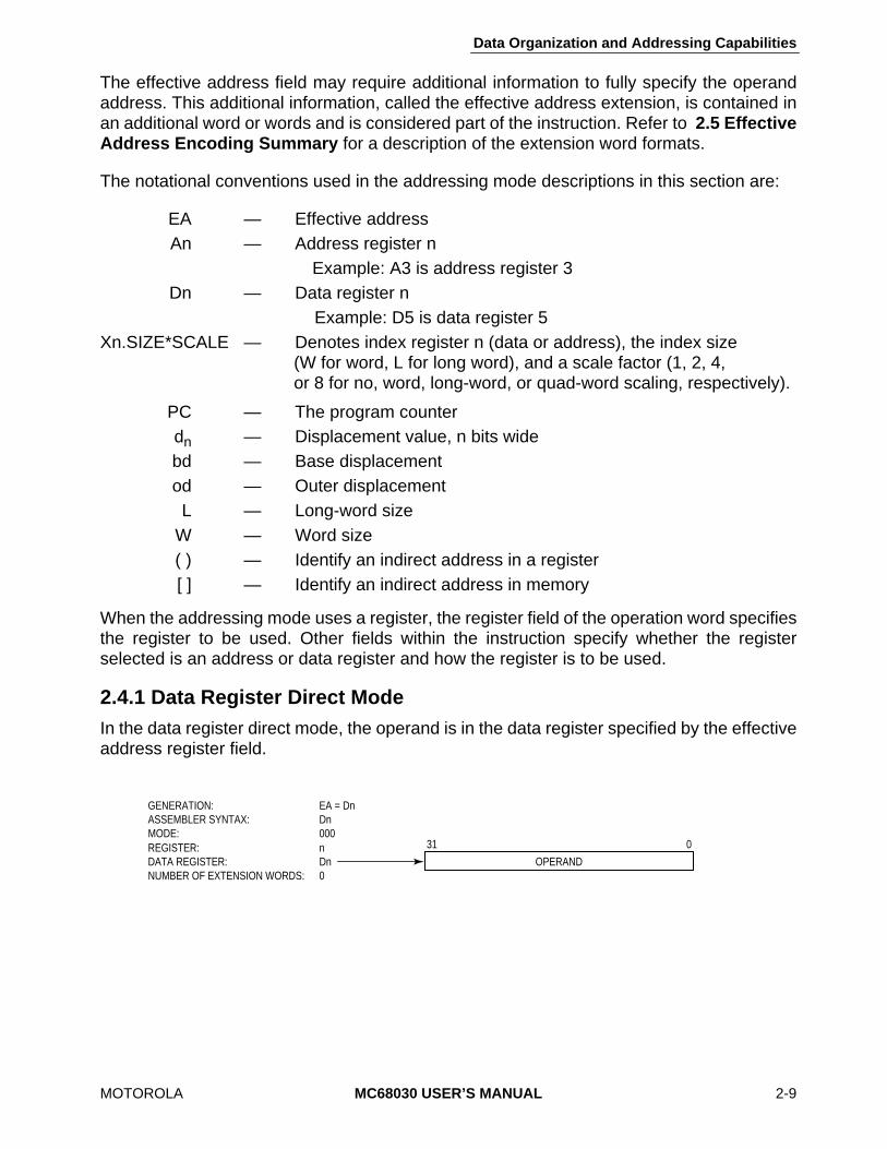
Data Organization and Addressing Capabilities
MOTOROLA
MC68030 USER’S MANUAL
2-9
The effective address field may require additional information to fully specify the operandaddress. This additional information, called the effective address extension, is contained inan additional word or words and is considered part of the instruction. Refer to
2.5 EffectiveAddress Encoding Summary
for a description of the extension word formats.
The notational conventions used in the addressing mode descriptions in this section are:
EA — Effective addressAn — Address register n
Example: A3 is address register 3Dn — Data register n
Example: D5 is data register 5Xn.SIZE*SCALE — Denotes index register n (data or address), the index size
(W for word, L for long word), and a scale factor (1, 2, 4, or 8 for no, word, long-word, or quad-word scaling, respectively).
PC — The program counterd
n
— Displacement value, n bits widebd — Base displacementod — Outer displacementL — Long-word size
W — Word size( ) — Identify an indirect address in a register[ ] — Identify an indirect address in memory
When the addressing mode uses a register, the register field of the operation word specifiesthe register to be used. Other fields within the instruction specify whether the registerselected is an address or data register and how the register is to be used.
2.4.1 Data Register Direct Mode
In the data register direct mode, the operand is in the data register specified by the effectiveaddress register field.
OPERAND
GENERATION:ASSEMBLER SYNTAX:MODE:REGISTER:DATA REGISTER:NUMBER OF EXTENSION WORDS:
EA = DnDn000nDn0
31 0
OPERAND
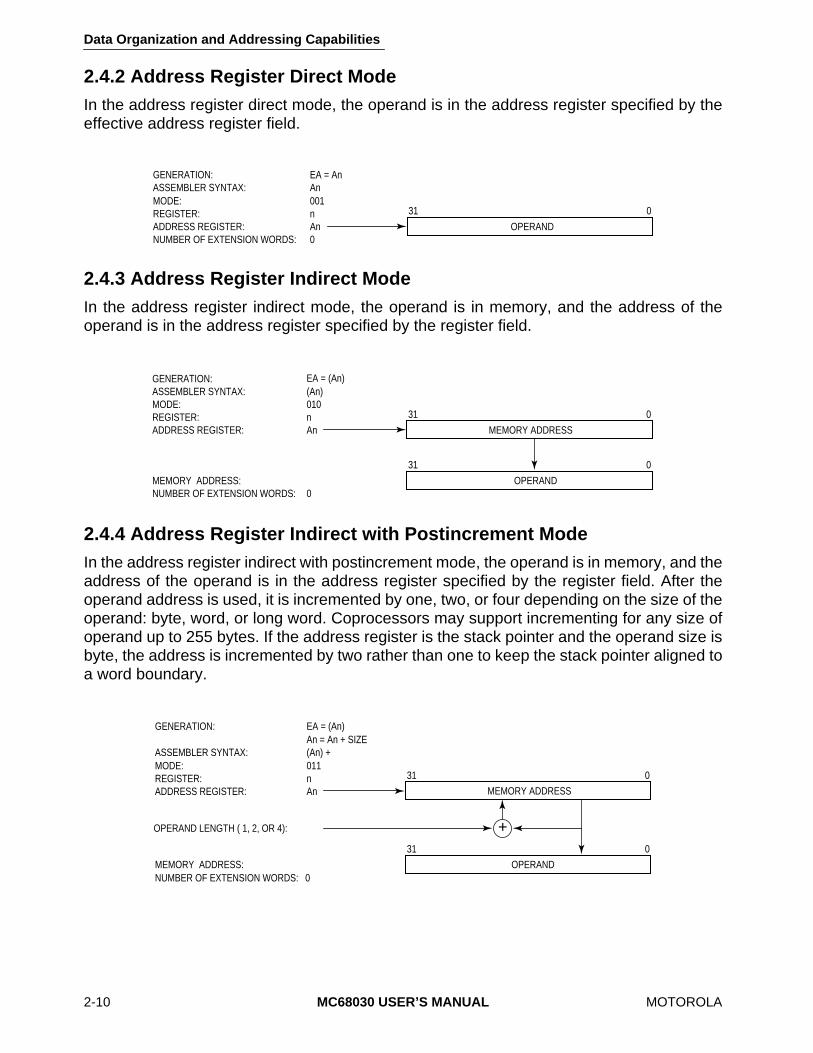
Data Organization and Addressing Capabilities
2-10
MC68030 USER’S MANUAL
MOTOROLA
2.4.2 Address Register Direct Mode
In the address register direct mode, the operand is in the address register specified by theeffective address register field.
2.4.3 Address Register Indirect Mode
In the address register indirect mode, the operand is in memory, and the address of theoperand is in the address register specified by the register field.
2.4.4 Address Register Indirect with Postincrement Mode
In the address register indirect with postincrement mode, the operand is in memory, and theaddress of the operand is in the address register specified by the register field. After theoperand address is used, it is incremented by one, two, or four depending on the size of theoperand: byte, word, or long word. Coprocessors may support incrementing for any size ofoperand up to 255 bytes. If the address register is the stack pointer and the operand size isbyte, the address is incremented by two rather than one to keep the stack pointer aligned toa word boundary.
31 0
OPERAND
EA = AnAn001nAn0
GENERATION:ASSEMBLER SYNTAX:MODE:REGISTER:ADDRESS REGISTER:NUMBER OF EXTENSION WORDS:
31 0
31 0
GENERATION:ASSEMBLER SYNTAX:MODE:REGISTER:ADDRESS REGISTER:
MEMORY ADDRESS:NUMBER OF EXTENSION WORDS:
EA = (An)(An)010nAn
OPERAND
MEMORY ADDRESS
0
31 0
31 0
+
MEMORY ADDRESS
OPERANDMEMORY ADDRESS:NUMBER OF EXTENSION WORDS:
OPERAND LENGTH ( 1, 2, OR 4):
GENERATION:
ASSEMBLER SYNTAX:MODE:REGISTER:ADDRESS REGISTER:
0
EA = (An)An = An + SIZE(An) +011nAn
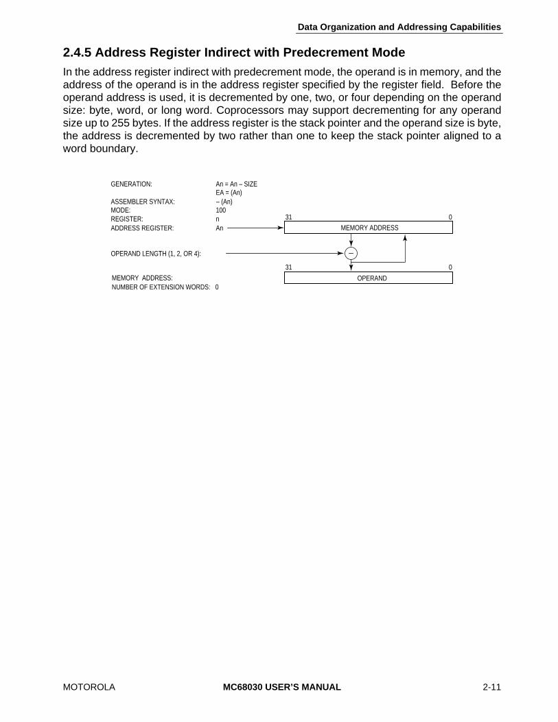
Data Organization and Addressing Capabilities
MOTOROLA
MC68030 USER’S MANUAL
2-11
2.4.5 Address Register Indirect with Predecrement Mode
In the address register indirect with predecrement mode, the operand is in memory, and theaddress of the operand is in the address register specified by the register field. Before theoperand address is used, it is decremented by one, two, or four depending on the operandsize: byte, word, or long word. Coprocessors may support decrementing for any operandsize up to 255 bytes. If the address register is the stack pointer and the operand size is byte,the address is decremented by two rather than one to keep the stack pointer aligned to aword boundary.
31 0
31 0
MEMORY ADDRESS
OPERANDMEMORY ADDRESS:NUMBER OF EXTENSION WORDS: 0
OPERAND LENGTH (1, 2, OR 4):
An = An – SIZEEA = (An)
– (An)100nAn
GENERATION:
ASSEMBLER SYNTAX:MODE:REGISTER:ADDRESS REGISTER:
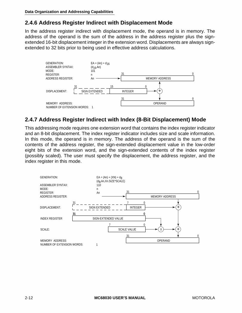
Data Organization and Addressing Capabilities
2-12
MC68030 USER’S MANUAL
MOTOROLA
2.4.6 Address Register Indirect with Displacement Mode
In the address register indirect with displacement mode, the operand is in memory. Theaddress of the operand is the sum of the address in the address register plus the sign-extended 16-bit displacement integer in the extension word. Displacements are always sign-extended to 32 bits prior to being used in effective address calculations.
2.4.7 Address Register Indirect with Index (8-Bit Displacement) Mode
This addressing mode requires one extension word that contains the index register indicatorand an 8-bit displacement. The index register indicator includes size and scale information.In this mode, the operand is in memory. The address of the operand is the sum of thecontents of the address register, the sign-extended displacement value in the low-ordereight bits of the extension word, and the sign-extended contents of the index register(possibly scaled). The user must specify the displacement, the address register, and theindex register in this mode.
31 0
31 0
EA = (An) + d(d ,An)101nAn
GENERATION:ASSEMBLER SYNTAX:MODE:REGISTER:ADDRESS REGISTER:
MEMORY ADDRESS:NUMBER OF EXTENSION WORDS: 1
OPERAND
+SIGN EXTENDED INTEGER
031 15
1616
MEMORY ADDRESS
DISPLACEMENT:
31 0
31 0
31 0
MEMORY ADDRESS
OPERANDMEMORY ADDRESS:NUMBER OF EXTENSION WORDS:
EA = (An) + (XN) + d(d ,An,Xn.SIZE*SCALE)110nAn
GENERATION:
ASSEMBLER SYNTAX:MODE:REGISTER:ADDRESS REGISTER:
INTEGER
SIGN-EXTENDED VALUE
SCALE VALUE
+0
0
+X
31
DISPLACEMENT:
INDEX REGISTER
SCALE:
1
7 0
7
SIGN EXTENDED
88
31

Data Organization and Addressing Capabilities
MOTOROLA
MC68030 USER’S MANUAL
2-13
2.4.8 Address Register Indirect with Index (Base Displacement) Mode
This addressing mode requires an index register indicator and an optional 16- or 32-bit sign-extended base displacement. The index register indicator includes size and scalinginformation. The operand is in memory. The address of the operand is the sum of thecontents of the address register, the scaled contents of the sign-extended index register,and the base displacement.
In this mode, the address register, the index register, and the displacement are all optional.If none is specified, the effective address is zero. This mode provides a data register indirectaddress when no address register is specified and the index register is a data register (Dn).
31 0
31 0
31 0
31 0
MEMORY ADDRESS:NUMBER OF EXTENSION WORDS: 1,2, OR 3
EA = (An) + (Xn) + bd(bd,An,Xn.SIZE*SCALE)110nAn
GENERATION:ASSEMBLER SYNTAX:MODE:REGISTER:ADDRESS REGISTER:
SIGN-EXTENDED VALUE
SIGN-EXTENDED VALUE
SCALE VALUE
OPERAND
+
+X
BASE DISPLACEMENT:
INDEX REGISTER:
SCALE:
MEMORY ADDRESS
7 0

Data Organization and Addressing Capabilities
2-14
MC68030 USER’S MANUAL
MOTOROLA
2.4.9 Memory Indirect Postindexed Mode
In this mode, the operand and its address are in memory. The processor calculates anintermediate indirect memory address using the base register (An) and base displacement(bd). The processor accesses a long word at this address and adds the index operand(Xn.SIZE*SCALE) and the outer displacement to yield the effective address. Bothdisplacements and the index register contents are sign-extended to 32 bits.
In the syntax for this mode, brackets enclose the values used to calculate the intermediatememory address. All four user-specified values are optional. Both the base and outerdisplacements may be null, word, or long word. When a displacement is omitted or anelement is suppressed, its value is taken as zero in the effective address calculation.
31 0
31 0
31 0
31 0
31 0
31 0
EFFECTIVE ADDRESS:NUMBER OF EXTENSION WORDS: 1,2, 3, 4, OR 5
EA = (bd + An) + Xn.SIZE*SCALE + od([bd,An],Xn.SIZE*SCALE,od)110An
GENERATION:ASSEMBLER SYNTAX:MODE:ADDRESS REGISTER:
SIGN-EXTENDED VALUE
SCALE VALUE
OPERAND
+
+
31 0
BASE DISPLACEMENT:
INDEX REGISTER:
SCALE:
MEMORY ADDRESS
INDIRECT MEMORY ADDRESS
VALUE AT INDIRECT MEMORY ADDRESS
POINTS TO
SIGN-EXTENDED VALUE
SIGN-EXTENDED VALUE
+X
OUTER DISPLACEMENT:
07
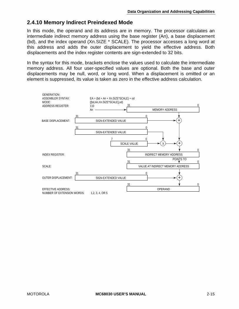
Data Organization and Addressing Capabilities
MOTOROLA
MC68030 USER’S MANUAL
2-15
2.4.10 Memory Indirect Preindexed Mode
In this mode, the operand and its address are in memory. The processor calculates anintermediate indirect memory address using the base register (An), a base displacement(bd), and the index operand (Xn.SIZE * SCALE). The processor accesses a long word atthis address and adds the outer displacement to yield the effective address. Bothdisplacements and the index register contents are sign-extended to 32 bits.
In the syntax for this mode, brackets enclose the values used to calculate the intermediatememory address. All four user-specified values are optional. Both the base and outerdisplacements may be null, word, or long word. When a displacement is omitted or anelement is suppressed, its value is taken as zero in the effective address calculation.
31 0
SIGN-EXTENDED VALUE
31 0
31 0
31 0
31 0
31 0
31 0
EFFECTIVE ADDRESS:NUMBER OF EXTENSION WORDS: 1,2, 3, 4, OR 5
EA = (bd + An + Xn.SIZE*SCALE) + od([bd,An,Xn.SIZE*SCALE],od)110An
GENERATION:ASSEMBLER SYNTAX:MODE:ADDRESS REGISTER:
SCALE VALUE
OPERAND
+
7
+BASE DISPLACEMENT:
INDEX REGISTER:
SCALE:
MEMORY ADDRESS
INDIRECT MEMORY ADDRESS
VALUE AT INDIRECT MEMORY ADDRESS
POINTS TO
SIGN-EXTENDED VALUE
SIGN-EXTENDED VALUE
+X
OUTER DISPLACEMENT:
0
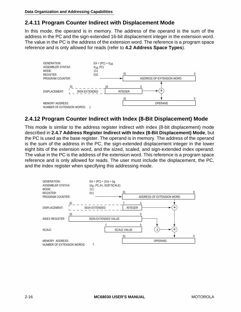
Data Organization and Addressing Capabilities
2-16
MC68030 USER’S MANUAL
MOTOROLA
2.4.11 Program Counter Indirect with Displacement Mode
In this mode, the operand is in memory. The address of the operand is the sum of theaddress in the PC and the sign-extended 16-bit displacement integer in the extension word.The value in the PC is the address of the extension word. The reference is a program spacereference and is only allowed for reads (refer to
4.2 Address Space Types
).
2.4.12 Program Counter Indirect with Index (8-Bit Displacement) Mode
This mode is similar to the address register indirect with index (8-bit displacement) modedescribed in
2.4.7 Address Register Indirect with Index (8-Bit Displacement) Mode
, butthe PC is used as the base register. The operand is in memory. The address of the operandis the sum of the address in the PC, the sign-extended displacement integer in the lowereight bits of the extension word, and the sized, scaled, and sign-extended index operand.The value in the PC is the address of the extension word. This reference is a program spacereference and is only allowed for reads. The user must include the displacement, the PC,and the index register when specifying this addressing mode.
31 0
31 0
EA = (PC) + dd ,PC)111010
GENERATION:ASSEMBLER SYNTAX:MODE:REGISTER:PROGRAM COUNTER:
MEMORY ADDRESS:NUMBER OF EXTENSION WORDS: 1
OPERAND
+ SIGN EXTENDED
031 15
1616
ADDRESS OF EXTENSION WORD
DISPLACEMENT: INTEGER
31 0
31 0
31 0
31 0
EA = (PC) + (Xn) + d(d , PC,Xn. SIZE*SCALE)111011
+
OPERANDMEMORY ADDRESS:NUMBER OF EXTENSION WORDS:
GENERATION:ASSEMBLER SYNTAX:MODE:REGISTER:PROGRAM COUNTER:
INTEGER
SIGN-EXTENDED VALUE
SCALE VALUE +X
DISPLACEMENT:
INDEX REGISTER
SCALE:
1
ADDRESS OF EXTENSION WORD
SIGN EXTENDED
7
88
7 0

Data Organization and Addressing Capabilities
MOTOROLA
MC68030 USER’S MANUAL
2-17
2.4.13 Program Counter Indirect with Index (Base Displacement) Mode
This mode is similar to the address register indirect with index (base displacement) modedescribed in
2.4.8 Address Register Indirect with Index (Base Displacement) Mode
, butthe PC is used as the base register. It requires an index register indicator and an optional16- or 32-bit sign-extended base displacement. The operand is in memory. The address ofthe operand is the sum of the contents of the PC, the scaled contents of the sign-extendedindex register, and the base displacement. The value of the PC is the address of the firstextension word. The reference is a program space reference and is only allowed for reads(refer to
4.2 Address Space Types
).
In this mode, the PC, the index register, and the displacement are all optional. However, theuser must supply the assembler notation "ZPC'' (zero value is taken for the PC) to indicatethat the PC is not used. This allows the user to access the program space without using thePC in calculating the effective address. The user can access the program space with a dataregister indirect access by placing ZPC in the instruction and specifying a data register (Dn)as the index register.
31 0
31 0
31 0
31 0
EA = (PC) + (Xn) + bd(bd, PC, Xn. SIZE*SCALE)111011
+
OPERANDMEMORY ADDRESS:NUMBER OF EXTENSION WORDS:
GENERATION:ASSEMBLER SYNTAX:MODE:REGISTER:PROGRAM COUNTER:
SIGN-EXTENDED VALUE
SCALE VALUE +X
BASE DISPLACEMENT:
INDEX REGISTER
SCALE:
1, 2 OR 3
ADDRESS OF EXTENSION WORD
SIGN-EXTENDED VALUE
07
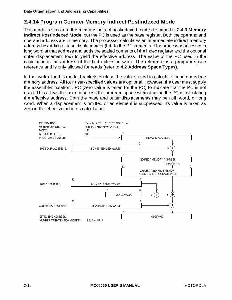
Data Organization and Addressing Capabilities
2-18 MC68030 USER’S MANUAL MOTOROLA
2.4.14 Program Counter Memory Indirect Postindexed ModeThis mode is similar to the memory indirect postindexed mode described in 2.4.9 MemoryIndirect Postindexed Mode, but the PC is used as the base register. Both the operand andoperand address are in memory. The processor calculates an intermediate indirect memoryaddress by adding a base displacement (bd) to the PC contents. The processor accesses along word at that address and adds the scaled contents of the index register and the optionalouter displacement (od) to yield the effective address. The value of the PC used in thecalculation is the address of the first extension word. The reference is a program spacereference and is only allowed for reads (refer to 4.2 Address Space Types).
In the syntax for this mode, brackets enclose the values used to calculate the intermediatememory address. All four user-specified values are optional. However, the user must supplythe assembler notation ZPC (zero value is taken for the PC) to indicate that the PC is notused. This allows the user to access the program space without using the PC in calculatingthe effective address. Both the base and outer displacements may be null, word, or longword. When a displacement is omitted or an element is suppressed, its value is taken aszero in the effective address calculation.
31 0
31 0
31 0
31 0
31 0
31 0
EFFECTIVE ADDRESS:NUMBER OF EXTENSION WORDS: 1,2, 3, 4, OR 5
EA = (bd + PC) + Xn.SIZE*SCALE + od([bd, PC], Xn.SIZE*SCALE,od)111011
GENERATION:ASSEMBLER SYNTAX:MODE:REGISTER FIELD:PROGRAM COUNTER:
SIGN-EXTENDED VALUE
SCALE VALUE
OPERAND
+
+
31 0
BASE DISPLACEMENT:
INDEX REGISTER:
MEMORY ADDRESS
INDIRECT MEMORY ADDRESS
VALUE AT INDIRECT MEMORYADDRESS IN PROGRAM SPACE
POINTS TO
SIGN-EXTENDED VALUE
SIGN-EXTENDED VALUE
+X
OUTER DISPLACEMENT:
07

Data Organization and Addressing Capabilities
MOTOROLA MC68030 USER’S MANUAL 2-19
2.4.15 Program Counter Memory Indirect Preindexed ModeThis mode is similar to the memory indirect preindexed mode described in 2.4.10 MemoryIndirect Preindexed Mode, but the PC is used as the base register. Both the operand andoperand address are in memory. The processor calculates an intermediate indirect memoryaddress by adding the PC contents, a base displacement (bd), and the scaled contents ofan index register. The processor accesses a long word at that address and adds the optionalouter displacement (od) to yield the effective address. The value of the PC is the address ofthe first extension word. The reference is a program space reference and is only allowed forreads (refer to 4.2 Address Space Types).
In the syntax for this mode, brackets enclose the values used to calculate the intermediatememory address. All four user-specified values are optional. However, the user must supplythe assembler notation ZPC (zero value is taken for the PC) to indicate that the PC is notused. This allows the user to access the program space without using the PC in calculatingthe effective address. Both the base and outer displacements may be null, word, or longword. When a displacement is omitted or an element is suppressed, its value is taken aszero in the effective address calculation.
31 0
31 0
31 0
31 0
31 0
31 0
31 0
EA = (bd + PC + Xn . SIZE * SCALE) + od([bd, PC, Xn. SIZE*SCALE],od)111011
+
OPERANDEFFECTIVE ADDRESS:NUMBER OF EXTENSION WORDS:
GENERATION:ASSEMBLER SYNTAX:MODE:REGISTER FIELD:PROGRAM COUNTER:
SIGN-EXTENDED VALUE
SCALE VALUE +X
BASE DISPLACEMENT:
INDEX REGISTER
1, 2, 3, 4 OR 5
ADDRESS OF EXTENSION WORD
SIGN-EXTENDED VALUE
INDIRECT MEMORY ADDRESS
POINTS TO
VALUE AT INDIRECT MEMORYADDRESS IN PROGRAM SPACE
SIGN-EXTENDED VALUE +OUTER DISPLACEMENT:
07

Data Organization and Addressing Capabilities
2-20 MC68030 USER’S MANUAL MOTOROLA
2.4.16 Absolute Short Addressing ModeIn this addressing mode, the operand is in memory, and the address of the operand is in theextension word. The 16-bit address is sign-extended to 32 bits before it is used.
2.4.17 Absolute Long Addressing ModeIn this mode, the operand is in memory, and the address of the operand occupies the twoextension words following the instruction word in memory. The first extension word containsthe high-order part of the address; the low-order part of the address is the second extensionword.
31 0
31 0OPERAND
MEMORY ADDRESSSIGN EXTENDED
15
GENERATION:ASSEMBLER SYNTAX:MODE:REGISTER FIELD:EXTENSION WORD:
EA GIVEN(xxx).W111000
MEMORY ADDRESS:NUMBER OF EXTENSION WORDS: 1
31 0
31 0
GENERATION:ASSEMBLER SYNTAX:MODE:REGISTER FIELD:FIRST EXTENSION WORD:
EA GIVEN(xxx).L111001
CONCATENATION
OPERAND
SECOND EXTENSION WORD:
MEMORY ADDRESS:NUMBER OF EXTENSION WORDS: 2
ADDRESS HIGH
ADDRESS LOW
0
015
15
Data Organization and Addressing Capabilities
MOTOROLA MC68030 USER’S MANUAL 2-21
2.4.18 Immediate DataIn this addressing mode, the operand is in one or two extension words:
Byte Operation
Operand is in the low-order byte of the extension word
Word Operation
Operand is in the extension word
Long-Word Operation
The high-order 16 bits of the operand are in the first extension word; the low-order 16bits are in the second extension word.
Coprocessor instructions can support immediate data of any size. The instruction word isfollowed by as many extension words as are required.
Generation: Operand givenAssembler Syntax: #xxxMode Field: 111Register Field: 100Number of Extension Words: 1 or 2, except for coprocessor instructions

Data Organization and Addressing Capabilities
2-22 MC68030 USER’S MANUAL MOTOROLA
2.5 EFFECTIVE ADDRESS ENCODING SUMMARYMost of the addressing modes use one of the three formats shown in Figure 2–4. The singleeffective address instruction is in the format of the instruction word. The encoding of themode field of this word selects the addressing mode. The register field contains the generalregister number or a value that selects the addressing mode when the mode field contains"111.'' Table 2–2 shows the encoding of these fields. Some indexed or indirect modes usethe instruction word followed by the brief format extension word. Other indexed or indirectmodes consist of the instruction word and the full format of extension words. The longestinstruction for the MC68030 contains 10 extension words. It is a MOVE instruction with fullformat extension words for both source and destination effective addresses and with 32-bitbase displacements and 32-bit outer displacements for both addresses. However,coprocessor instructions can have any number of extension words. Refer to the coprocessorinstruction formats in Section 10 Coprocessor Interface Description.
For effective addresses that use the full format, the index suppress (IS) bit and the index/indirect selection (I/IS) field determine the type of indexing and indirection. Table 2–1 liststhe indexing and indirection operations corresponding to all combinations of IS and I/ISvalues.
Table 2-1. IS–I/IS Memory Indirection Encodings
IS Index/Indirect Operation0 000 No Memory Indirection0 001 Indirect Preindexed with Null Outer Displacement0 010 Indirect Preindexed with Word Outer Displacement0 011 Indirect Preindexed with Long Outer Displacement0 100 Reserved0 101 Indirect Postindexed with Mull Outer Displacement0 110 Indirect Postindexed with Word Outer Displacement0 111 Indirect Postindexed with Long Outer Displacement1 000 No Memory Indirection1 001 Memory Indirect with Mull Outer Displacement1 010 Memory Indirect with Word Outer Displacement1 011 Memory Indirect with Long Outer Displacement1 100–111 Reserved
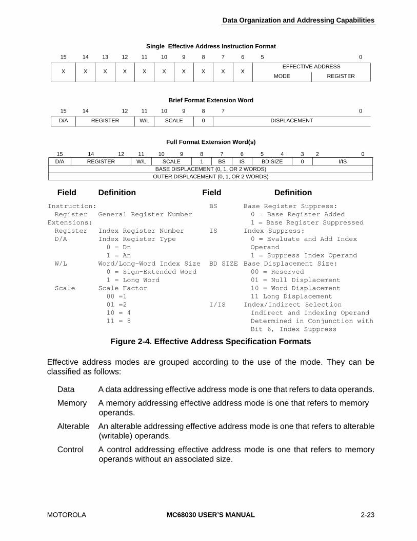
Data Organization and Addressing Capabilities
MOTOROLA MC68030 USER’S MANUAL 2-23
Field Definition Field Definition
Instruction: BS Base Register Suppress:Register General Register Number 0 = Base Register Added
Extensions: 1 = Base Register Suppressed Register Index Register Number IS Index Suppress: D/A Index Register Type 0 = Evaluate and Add Index
0 = Dn Operand1 = An 1 = Suppress Index Operand
W/L Word/Long-Word Index Size BD SIZE Base Displacement Size:0 = Sign-Extended Word 00 = Reserved1 = Long Word 01 = Null Displacement
Scale Scale Factor 10 = Word Displacement00 =1 11 Long Displacement01 =2 I/IS Index/Indirect Selection10 = 4 Indirect and Indexing Operand11 = 8 Determined in Conjunction with
Bit 6, Index Suppress
Figure 2-4. Effective Address Specification Formats
Effective address modes are grouped according to the use of the mode. They can beclassified as follows:
Data A data addressing effective address mode is one that refers to data operands.
Memory A memory addressing effective address mode is one that refers to memory operands.
Alterable An alterable addressing effective address mode is one that refers to alterable(writable) operands.
Control A control addressing effective address mode is one that refers to memoryoperands without an associated size.
Single Effective Address Instruction Format
15 14 13 12 11 10 9 8 7 6 5 0
X X X X X X X X X XEFFECTIVE ADDRESS
MODE REGISTER
Brief Format Extension Word
15 14 12 11 10 9 8 7 0
D/A REGISTER W/L SCALE 0 DISPLACEMENT
Full Format Extension Word(s)
15 14 12 11 10 9 8 7 6 5 4 3 2 0D/A REGISTER W/L SCALE 1 BS IS BD SIZE 0 I/IS
BASE DISPLACEMENT (0, 1, OR 2 WORDS)OUTER DISPLACEMENT (0, 1, OR 2 WORDS)
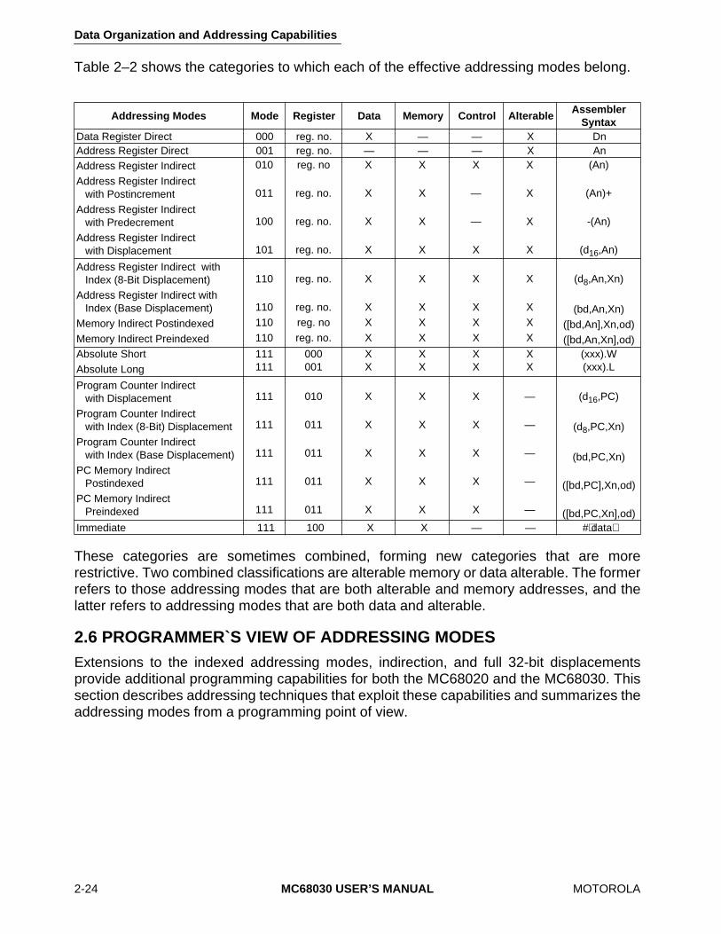
Data Organization and Addressing Capabilities
2-24 MC68030 USER’S MANUAL MOTOROLA
Table 2–2 shows the categories to which each of the effective addressing modes belong.
These categories are sometimes combined, forming new categories that are morerestrictive. Two combined classifications are alterable memory or data alterable. The formerrefers to those addressing modes that are both alterable and memory addresses, and thelatter refers to addressing modes that are both data and alterable.
2.6 PROGRAMMER`S VIEW OF ADDRESSING MODESExtensions to the indexed addressing modes, indirection, and full 32-bit displacementsprovide additional programming capabilities for both the MC68020 and the MC68030. Thissection describes addressing techniques that exploit these capabilities and summarizes theaddressing modes from a programming point of view.
Addressing Modes Mode Register Data Memory Control AlterableAssembler
SyntaxData Register Direct 000 reg. no. X — — X DnAddress Register Direct 001 reg. no. — — — X AnAddress Register IndirectAddress Register Indirect
with PostincrementAddress Register Indirect
with PredecrementAddress Register Indirect
with Displacement
010
011
100
101
reg. no
reg. no.
reg. no.
reg. no.
X
X
X
X
X
X
X
X
X
—
—
X
X
X
X
X
(An)
(An)+
-(An)
(d16,An)
Address Register Indirect withIndex (8-Bit Displacement)
Address Register Indirect withIndex (Base Displacement)
Memory Indirect PostindexedMemory Indirect Preindexed
110
110110110
reg. no.
reg. no.reg. noreg. no.
X
XXX
X
XXX
X
XXX
X
XXX
(d8,An,Xn)
(bd,An,Xn)([bd,An],Xn,od)([bd,An,Xn],od)
Absolute ShortAbsolute Long
111111
000001
XX
XX
XX
XX
(xxx).W(xxx).L
Program Counter Indirectwith Displacement
Program Counter Indirect with Index (8-Bit) Displacement
Program Counter Indirect with Index (Base Displacement)
PC Memory Indirect Postindexed
PC Memory Indirect Preindexed
111
111
111
111
111
010
011
011
011
011
X
X
X
X
X
X
X
X
X
X
X
X
X
X
X
—
—
—
—
—
(d16,PC)
(d8,PC,Xn)
(bd,PC,Xn)
([bd,PC],Xn,od)
([bd,PC,Xn],od)Immediate 111 100 X X — — #⟨data⟩
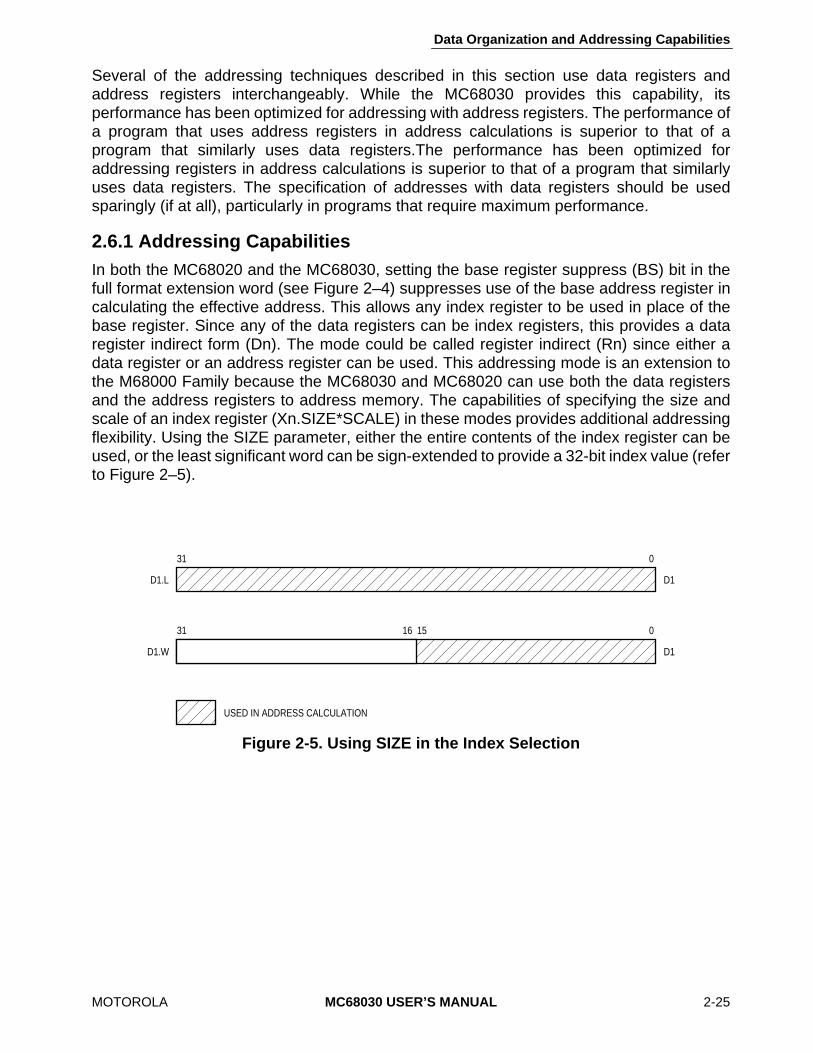
Data Organization and Addressing Capabilities
MOTOROLA MC68030 USER’S MANUAL 2-25
Several of the addressing techniques described in this section use data registers andaddress registers interchangeably. While the MC68030 provides this capability, itsperformance has been optimized for addressing with address registers. The performance ofa program that uses address registers in address calculations is superior to that of aprogram that similarly uses data registers.The performance has been optimized foraddressing registers in address calculations is superior to that of a program that similarlyuses data registers. The specification of addresses with data registers should be usedsparingly (if at all), particularly in programs that require maximum performance.
2.6.1 Addressing CapabilitiesIn both the MC68020 and the MC68030, setting the base register suppress (BS) bit in thefull format extension word (see Figure 2–4) suppresses use of the base address register incalculating the effective address. This allows any index register to be used in place of thebase register. Since any of the data registers can be index registers, this provides a dataregister indirect form (Dn). The mode could be called register indirect (Rn) since either adata register or an address register can be used. This addressing mode is an extension tothe M68000 Family because the MC68030 and MC68020 can use both the data registersand the address registers to address memory. The capabilities of specifying the size andscale of an index register (Xn.SIZE*SCALE) in these modes provides additional addressingflexibility. Using the SIZE parameter, either the entire contents of the index register can beused, or the least significant word can be sign-extended to provide a 32-bit index value (referto Figure 2–5).
Figure 2-5. Using SIZE in the Index Selection
D1.L
D1.W
D1
D1
31
16 1531 0
0
USED IN ADDRESS CALCULATION
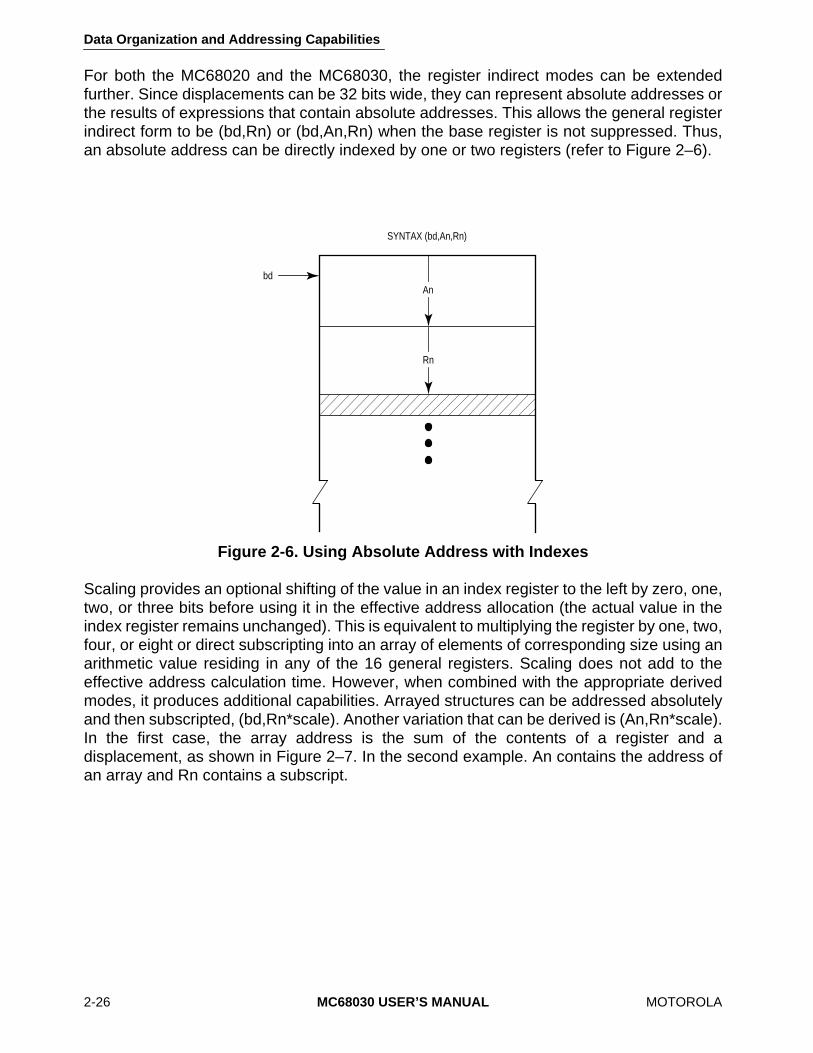
Data Organization and Addressing Capabilities
2-26 MC68030 USER’S MANUAL MOTOROLA
For both the MC68020 and the MC68030, the register indirect modes can be extendedfurther. Since displacements can be 32 bits wide, they can represent absolute addresses orthe results of expressions that contain absolute addresses. This allows the general registerindirect form to be (bd,Rn) or (bd,An,Rn) when the base register is not suppressed. Thus,an absolute address can be directly indexed by one or two registers (refer to Figure 2–6).
Scaling provides an optional shifting of the value in an index register to the left by zero, one,two, or three bits before using it in the effective address allocation (the actual value in theindex register remains unchanged). This is equivalent to multiplying the register by one, two,four, or eight or direct subscripting into an array of elements of corresponding size using anarithmetic value residing in any of the 16 general registers. Scaling does not add to theeffective address calculation time. However, when combined with the appropriate derivedmodes, it produces additional capabilities. Arrayed structures can be addressed absolutelyand then subscripted, (bd,Rn*scale). Another variation that can be derived is (An,Rn*scale).In the first case, the array address is the sum of the contents of a register and adisplacement, as shown in Figure 2–7. In the second example. An contains the address ofan array and Rn contains a subscript.
Figure 2-6. Using Absolute Address with Indexes
An
Rn
bd
SYNTAX (bd,An,Rn)
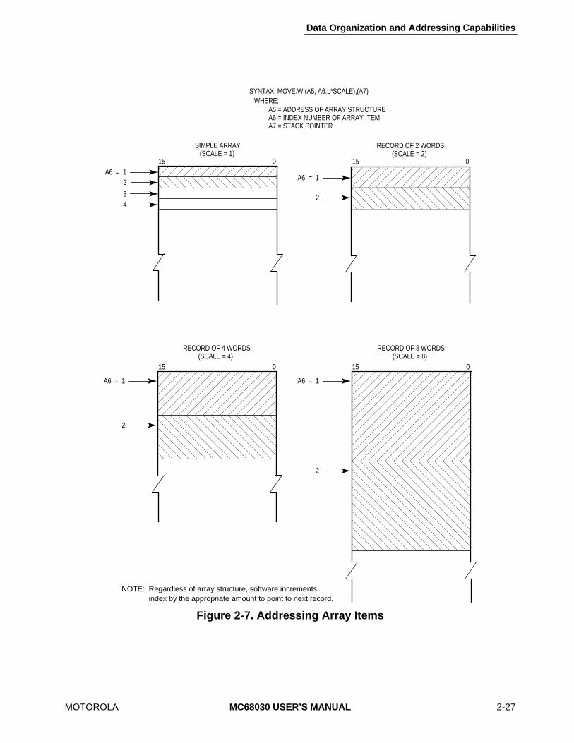
Data Organization and Addressing Capabilities
MOTOROLA MC68030 USER’S MANUAL 2-27
Figure 2-7. Addressing Array Items
A6 = 12
34
SIMPLE ARRAY(SCALE = 1)
RECORD OF 2 WORDS(SCALE = 2)
A6 = 1
2
2
A6 = 1
2
A6 = 1
15 015 0
SYNTAX: MOVE.W (A5, A6.L*SCALE),(A7)WHERE:
A5 = ADDRESS OF ARRAY STRUCTUREA6 = INDEX NUMBER OF ARRAY ITEMA7 = STACK POINTER
RECORD OF 4 WORDS(SCALE = 4)
RECORD OF 8 WORDS(SCALE = 8)
NOTE: Regardless of array structure, software increments index by the appropriate amount to point to next record.
15 0 15 0
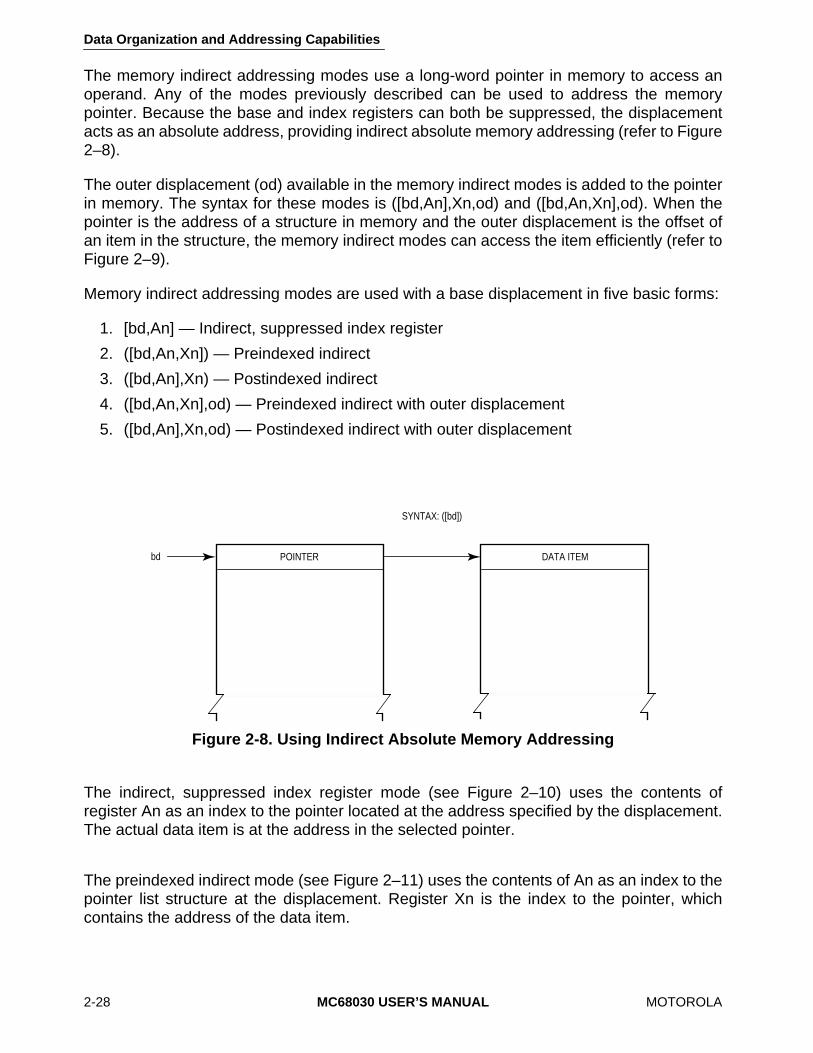
Data Organization and Addressing Capabilities
2-28 MC68030 USER’S MANUAL MOTOROLA
The memory indirect addressing modes use a long-word pointer in memory to access anoperand. Any of the modes previously described can be used to address the memorypointer. Because the base and index registers can both be suppressed, the displacementacts as an absolute address, providing indirect absolute memory addressing (refer to Figure2–8).
The outer displacement (od) available in the memory indirect modes is added to the pointerin memory. The syntax for these modes is ([bd,An],Xn,od) and ([bd,An,Xn],od). When thepointer is the address of a structure in memory and the outer displacement is the offset ofan item in the structure, the memory indirect modes can access the item efficiently (refer toFigure 2–9).
Memory indirect addressing modes are used with a base displacement in five basic forms:
1. [bd,An] — Indirect, suppressed index register
2. ([bd,An,Xn]) — Preindexed indirect
3. ([bd,An],Xn) — Postindexed indirect
4. ([bd,An,Xn],od) — Preindexed indirect with outer displacement
5. ([bd,An],Xn,od) — Postindexed indirect with outer displacement
The indirect, suppressed index register mode (see Figure 2–10) uses the contents ofregister An as an index to the pointer located at the address specified by the displacement.The actual data item is at the address in the selected pointer.
The preindexed indirect mode (see Figure 2–11) uses the contents of An as an index to thepointer list structure at the displacement. Register Xn is the index to the pointer, whichcontains the address of the data item.
Figure 2-8. Using Indirect Absolute Memory Addressing
POINTER DATA ITEMbd
SYNTAX: ([bd])

Data Organization and Addressing Capabilities
MOTOROLA MC68030 USER’S MANUAL 2-29
Figure 2-9. Accessing an Item in a Structure Using a Pointer
Figure 2-10. Indirect Addressing, Suppressed Index Register
POINTER
DATA ITEM
An
od
MEMORY STRUCTURE
SYNTAX: ([An],od)
POINTER DATA ITEM
bd
POINTER LIST
SYNTAX: ([bd,An])
An
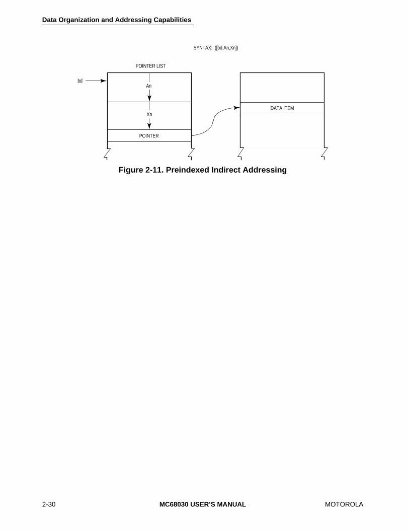
Data Organization and Addressing Capabilities
2-30 MC68030 USER’S MANUAL MOTOROLA
Figure 2-11. Preindexed Indirect Addressing
POINTER
DATA ITEM
bd
POINTER LIST
SYNTAX: ([bd,An,Xn])
Xn
An

Data Organization and Addressing Capabilities
MOTOROLA MC68030 USER’S MANUAL 2-31
The postindexed indirect mode (see Figure 2–12) uses the contents of An as an index to thepointer list at the displacement. Register Xn is used as an index to the structure of data itemslocated at the address specified by the pointer. Figure 2–13 shows the preindexed indirectaddressing with outer displacement mode.
Figure 2-12. Postindexed Indirect Addressing
Figure 2-13. Preindexed Indirect Addressing with Outer Displacement
POINTER DATA ITEM
bd
POINTER LIST
SYNTAX: ([bd,An],Xn)
Xn
An
POSTINDEXED STRUCTURE
POINTER DATA ITEM
bd
POINTER LIST
SYNTAX: ([bd,An,Xn],od)
od
An
Xn
STRUCTURE

Data Organization and Addressing Capabilities
2-32 MC68030 USER’S MANUAL MOTOROLA
The postindexed indirect mode with outer displacement (see Figure 2–14) uses the contentsof An as an index to the pointer list at the displacement. Register Xn is used as an index tothe structure of data structures at the address in the pointer. The outer displacement (od) isthe displacement of the data item within the selected data structure.
2.6.2 General Addressing Mode SummaryThe addressing modes described in the previous section are derived from specificcombinations of options in the indexing mode or a selection of two alternate addressingmodes. For example, the addressing mode called register indirect (Rn) assembles as theaddress register indirect if the register is an address register. If Rn is a data register, theassembler uses the address register indirect with index mode using the data register as theindirect register and suppresses the address register by setting the base suppress bit in theeffective address specification. Assigning an address register as Rn provides higherperformance than using a data register as Rn. Another case is (bd,An), which selects anaddressing mode depending on the size of the displacement. If the displacement is 16 bitsor less, the address register indirect with displacement mode (d16,An) is used. When a 32-bit displacement is required, the address register indirect with index (bd,An,Xn) is used withthe index register suppressed.
Figure 2-14. Postindexed Indirect Addressing with Outer Displacement
POINTER DATA ITEM
bd
POINTER LIST
SYNTAX: ([bd,An],Xn,od)
odAn
POSTINDEXED STRUCTUREWITH OUTER DISPLACEMENT
Xn
Data Organization and Addressing Capabilities
MOTOROLA MC68030 USER’S MANUAL 2-33
It is useful to examine the derived addressing modes available to a programmer (withoutregard to the MC68030 effective addressing mode actually encoded) because theprogrammer need not be concerned about these decisions. The assembler can choose themore efficient addressing mode to encode.
In the list of derived addressing modes that follows, common programming terms are used.The following definitions apply:
pointer — long-Word value in a register or in memory which represents anaddress.
base — A pointer combined with a displacement to represent an address.
index — A constant or variable value added into an effective address calcula-tion. A constant index is a displacement. A variable index is alwaysrepresented by a register containing the value.
disp — Displacement, a constant index.
subscript — The use of any of the data or address registers as a variable indexsubscript into arrays of items 1, 2, 4 or 8 bytes in size.
relative — An address calculated from the program counter contents. Theaddress is position independent and is in program space. All otheraddresses but psaddr are in data space.
addr — An absolute address.
psaddr — An absolute address in program space. All other addresses but PCrelative are in data space.
preindexed — All modes from absolute address through program counter relative.
postindexed— Any of the following modes:
addr — Absolute address in data space
psaddr,ZPC — Absolute address in program space
An — Register pointer with constant displacement
disp.An — Register pointer with constant displacement
addr,An — Absolute address with single variable name
disp,Pc — Simple PC relative
The addressing modes defined in programming terms, which are derivations of theaddressing modes provided by the MC68030 architecture, are as follows:
Immediate Data — #data:The data is a constant located in the instruction stream.
Register Direct — Rn:The contents of a register contain the operand.
Scanning Modes:(An)+
Data Organization and Addressing Capabilities
2-34 MC68030 USER’S MANUAL MOTOROLA
Address register pointer automatically incremented after use.
– (An)Address register pointer automatically decremented before use.
Absolute Address:(addr)
Absolute address in data space.
(psaddr,ZPC)Absolute address in program space. Symbol ZPC suppresses the PC,but retains PC relative mode to directly access the program space.
Register Pointer:(Rn)
Register as a pointer.
(disp,Rn)Register as a pointer with constant index (or base address).
Indexing
(An,Rn)
Register pointer An with variable index Rn.
(disp,An,Rn)
Register pointer with constant and variable index (or a base addresswith a variable index).
(addr,Rn)
Absolute address with two variable indexes.
Subscripting:
(An,Rn*scale)
Address register pointer subscript.
(disp,An,Rn*scale)
Address register pointer subscript with constant displacement(or base address with subscript).
(addr,Rn*scale)
Absolute address with subscript.
(addr,An,Rn*scale)
Absolute address subscript with variable index.
Program Relative:
Data Organization and Addressing Capabilities
MOTOROLA MC68030 USER’S MANUAL 2-35
(disp,PC)
Simple PC relative.
(disp,PC,Rn)
PC relative with variable index.
(disp,PC,Rn*scale)
PC relative with subscript.
Memory Pointer:
([preindexed])
Memory pointer directly to data operand.
([preindexed],disp)
Memory pointer as base with displacement to data operand.
([postindexed],Rn)
Memory pointer with variable index.
([postindexed],disp,Rn)
Memory pointer with constant and variable index.
([postindexed],Rn*scale)
Memory pointer subscripted.
([postindexed],disp,Rn*scale)
Memory pointer subscripted with constant index.
Data Organization and Addressing Capabilities
2-36 MC68030 USER’S MANUAL MOTOROLA
2.7 M68000 FAMILY ADDRESSING COMPATIBILITYPrograms can be easily transported from one member of the M68000 Family to another inan upward compatible fashion. The user object code of each early member of the family isupward compatible with newer members and can be executed on the newer microprocessorwithout change. The address extension word(s) are encoded with the information that allowsthe MC68020/MC68030 to distinguish the new address extension words for the earlyMC68000/MC68008/MC68010 microprocessors and for the newer 32-bit MC68020/MC68030 microprocessors are shown in Figure 2–15. Notice the encoding for SCALE usedby the MC68020/MC68030 is a compatible extension of the M68000 architecture. A valueof zero for SCALE is the same encoding for both extension words; hence, software that usesthis encoding is both upward and downward compatible across all processors in the productline. However, the other values of SCALE are not found in both extension formats; thus,while software can be easily migrated in an upward compatible direction, only nonscaledaddressing is supported in a downward fashion. If the MC68000 were to execute aninstruction that encoded a scaling factor, the scaling factor would be ignored and not accessthe desired memory address. The earlier microprocessors have no knowledge of theextension word formats implemented by newer processors; while they do detect illegalinstructions, they do not decode invalid encodings of the extension words as exceptions.
2.8 OTHER DATA STRUCTURESStacks and queues are widely used data structures. The MC68030 implements a systemstack and also provides instructions that support the use of user stacks and queues.
2.8.1 System StackAddress register seven (A7) is used as the system stack pointer (SP). Any of the threesystem stack registers is active at any one time. The M and S bits of the status registerdetermine which stack pointer is used. When S = 0 indicating user mode (user privilegelevel), the user stack pointer (USP) is the active system stack pointer, and the master andinterrupt stack pointers cannot be referenced. When S = 1 indicating supervisor mode (atsupervisor privilege level) and M = 1, the master stack pointer (MSP) is the active systemstack pointer. When S = 1 and M = 0, the interrupt stack pointer (ISP) is the active systemstack pointer. This mode is the MC68030 default mode after reset and corresponds to theMC68000, MC68008, and MC68010 supervisor mode. The term supervisor stack pointer(SSP) refers to the master or interrupt stack pointers, depending on the state of the M bit.When M = 1, the term SSP (or A7) refers to the MSP address register. When M = 0, the termis implicitly referenced by all instructions that use the system stack. Each system stack fillsfrom high to low memory.
Data Organization and Addressing Capabilities
MOTOROLA MC68030 USER’S MANUAL 2-37
A subroutine call saves the program counter on the active system stack, and the returnrestores it from the active system stack. During the processing of traps and interrupts, boththe program counter and the status register are saved on the supervisor stack (either masteror interrupt). Thus, the execution of supervisor code is independent of user code and thecondition of the user stack; conversely, user programs use the user stack pointerindependently of supervisor stack requirements.
To keep data on the system stack aligned for maximum efficiency, the active stack pointeris automatically decremented or incremented by two for all byte-sized operands moved toor from the stack. In long-word-organized memory, aligning the stack pointer on a long-wordaddress signed significantly increases the efficiency of stacking exception frames,subroutine calls and returns, and other stacking operations.
(UNABLE TO LOCATE ART. MUST BE RECREATED.)
Figure 2-15. M68000 Family Address Extension Words
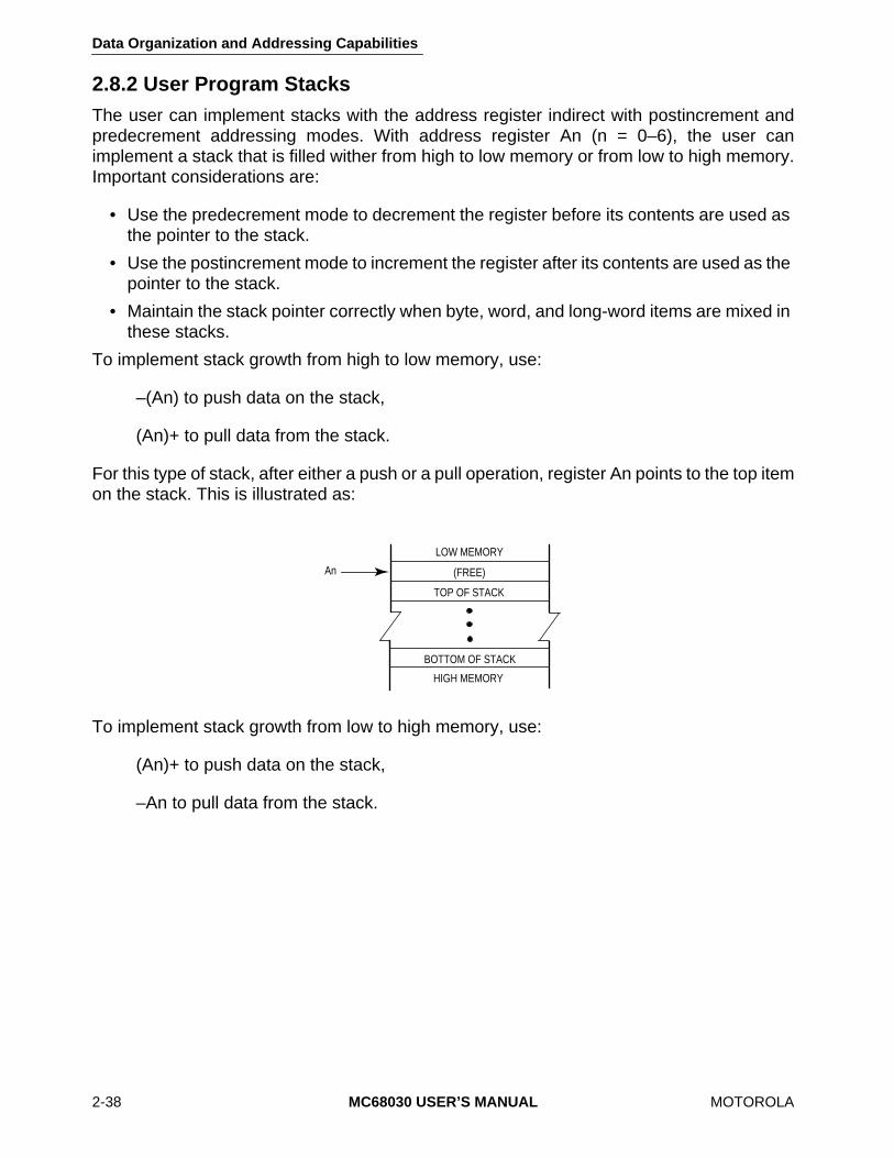
Data Organization and Addressing Capabilities
2-38 MC68030 USER’S MANUAL MOTOROLA
2.8.2 User Program StacksThe user can implement stacks with the address register indirect with postincrement andpredecrement addressing modes. With address register An (n = 0–6), the user canimplement a stack that is filled wither from high to low memory or from low to high memory.Important considerations are:
• Use the predecrement mode to decrement the register before its contents are used as the pointer to the stack.
• Use the postincrement mode to increment the register after its contents are used as the pointer to the stack.
• Maintain the stack pointer correctly when byte, word, and long-word items are mixed in these stacks.
To implement stack growth from high to low memory, use:
–(An) to push data on the stack,
(An)+ to pull data from the stack.
For this type of stack, after either a push or a pull operation, register An points to the top itemon the stack. This is illustrated as:
To implement stack growth from low to high memory, use:
(An)+ to push data on the stack,
–An to pull data from the stack.
An
LOW MEMORY
(FREE)
TOP OF STACK
BOTTOM OF STACK
HIGH MEMORY

Data Organization and Addressing Capabilities
MOTOROLA MC68030 USER’S MANUAL 2-39
In this case, after either a push or pull operation, register An points to the next availablespace on the stack. This is illustrated as:
2.8.3 QueuesThe user can implement queues with the address register indirect with postincrement orpredecrement addressing modes. Using a pair of address registers (who of A0–A6), the usercan implement a queue which is filled either from high to low memory or from low to highmemory. Two registers are used because queues are pushed from one end and pulled fromthe other. One register, An, contains the "put'' pointer; the other, Am, the "get'' pointer.
To implement growth of the queue from low to high memory, use:
(An)+ to put data into the queue,
(Am)+ to get data from the queue.
After a "put'' operation, the "put'' address register points to the next available space in thequeue, and the unchanged "get'' address register points to the next item to be removed fromthe queue. After a "get'' operation, the "get'' address register points to the next item to beremoved from the queue, and the unchanged "put'' address register points to the nextavailable space in the queue. This is illustrated as:
To implement the queue as a circular buffer, the relevant address register should bechecked and adjusted, if necessary, before performing the "put'' or "get'' operation. Theaddress register is adjusted by subtracting the buffer length (in bytes) from the register.
LOW MEMORY
TOP OF STACK
HIGH MEMORY
An
BOTTOM OF STACK
(FREE)
GET (Am) +
LOW MEMORY
(FREE)
HIGH MEMORY
LAST GET (FREE)
LAST PUT
NEXT GET
PUT (An) +
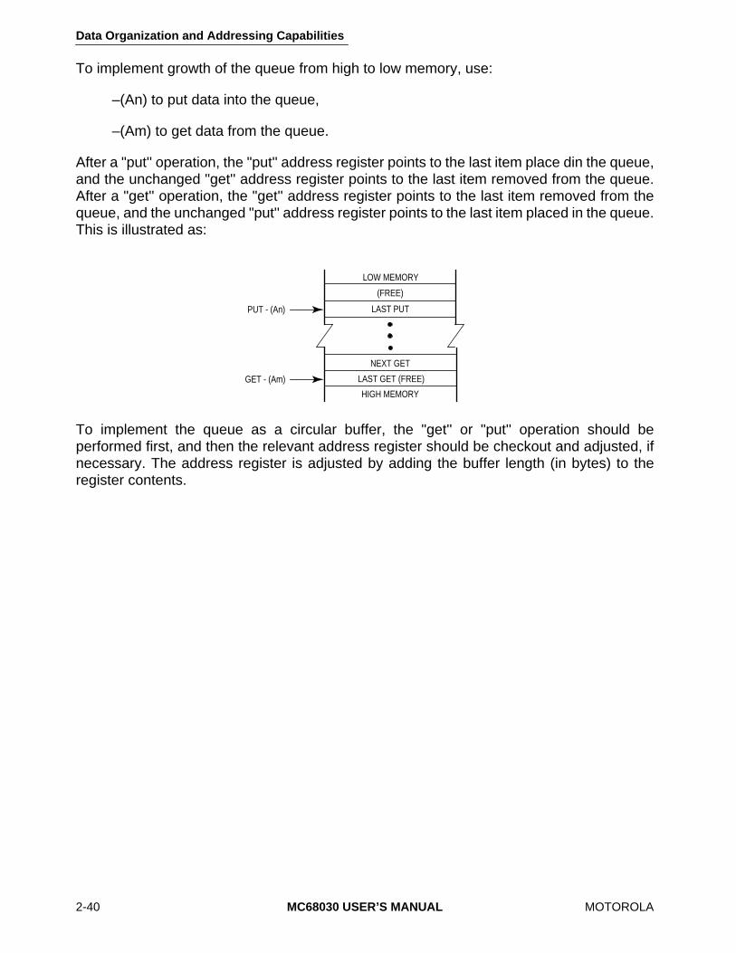
Data Organization and Addressing Capabilities
2-40 MC68030 USER’S MANUAL MOTOROLA
To implement growth of the queue from high to low memory, use:
–(An) to put data into the queue,
–(Am) to get data from the queue.
After a "put'' operation, the "put'' address register points to the last item place din the queue,and the unchanged "get'' address register points to the last item removed from the queue.After a "get'' operation, the "get'' address register points to the last item removed from thequeue, and the unchanged "put'' address register points to the last item placed in the queue.This is illustrated as:
To implement the queue as a circular buffer, the "get'' or "put'' operation should beperformed first, and then the relevant address register should be checkout and adjusted, ifnecessary. The address register is adjusted by adding the buffer length (in bytes) to theregister contents.
LOW MEMORY
(FREE)
HIGH MEMORY
LAST GET (FREE)
LAST PUT
NEXT GET
PUT - (An)
GET - (Am)
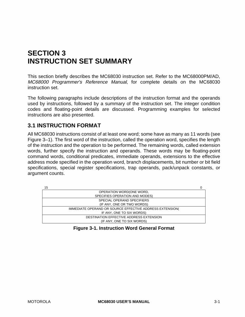
MOTOROLA
MC68030 USER’S MANUAL
3-1
SECTION 3INSTRUCTION SET SUMMARY
This section briefly describes the MC68030 instruction set. Refer to the MC68000PM/AD,
MC68000 Programmer's Reference Manual
, for complete details on the MC68030instruction set.
The following paragraphs include descriptions of the instruction format and the operandsused by instructions, followed by a summary of the instruction set. The integer conditioncodes and floating-point details are discussed. Programming examples for selectedinstructions are also presented.
3.1 INSTRUCTION FORMAT
All MC68030 instructions consist of at least one word; some have as many as 11 words (seeFigure 3–1). The first word of the instruction, called the operation word, specifies the lengthof the instruction and the operation to be performed. The remaining words, called extensionwords, further specify the instruction and operands. These words may be floating-pointcommand words, conditional predicates, immediate operands, extensions to the effectiveaddress mode specified in the operation word, branch displacements, bit number or bit fieldspecifications, special register specifications, trap operands, pack/unpack constants, orargument counts.
Figure 3-1. Instruction Word General Format
15 0OPERATION WORD(ONE WORD,
SPECIFIES OPERATION AND MODES)SPECIAL OPERAND SPECIFIERS(IF ANY, ONE OR TWO WORDS)
IMMEDIATE OPERAND OR SOURCE EFFECTIVE ADDRESS EXTENSION(IF ANY, ONE TO SIX WORDS)
DESTINATION EFFECTIVE ADDRESS EXTENSION(IF ANY, ONE TO SIX WORDS)
Instruction Set Summary
3-2
MC68030 USER’S MANUAL
MOTOROLA
Besides the operation code, which specifies the function to be performed, an instructiondefines the location of every operand for the function. Instructions specify an operandlocation in one of three ways:
1. Register Specification — A register field of the instruction contains the number of the register.
2. Effective Address — An effective address field of the instruction contains address mode information.
3. Implicit Reference — The definition of an instruction implies the use of specific regis-ters.
The register field within an instruction specifies the register to be used. Other fields withinthe instruction specify whether the register selected is an address or data register and howthe register is to be used.
Section 1 Introduction
contains register information.
Effective address information includes the registers, displacements, and absoluteaddresses for the effective address mode.
Section 2 Data Organization and AddressingCapabilities
describes the effective address modes in detail.
Certain instructions operate on specific registers. These instructions imply the requiredregisters.
3.2 INSTRUCTION SUMMARY
The instructions form a set of tools to perform the following operations:
Each instruction type is described in detail in the following paragraphs
Data MovementInteger ArithmeticLogicalShift and RotateBit Manipulation
Bit Field ManipulationBinary-Coded Decimal ArithmeticProgram ControlSystem ControlMultiprocessor Communications
Instruction Set Summary
MOTOROLA
MC68030 USER’S MANUAL
3-3
The following notations are used in this section. In the operand syntax statements of theinstruction definitions, the operand on the right is the destination operand.
An = any address register, A7–A0Dn = any data register, D7–D0Rn = any address or data register
CCR = condition code register (lower byte of status register)cc = condition codes from CCR
SR = status registerSP = active stack pointer
USP = user stack pointerISP = supervisor/interrupt stack pointer
MSP = supervisor/master stack pointerSSP = supervisor (master or interrupt) stack pointerDFC = destination function code registerSFC = source function code register
Rc = control register (VBR, SFC, DFC, CACR)
MRc= MMU control register (SRP, URP, TC, DTT0, DTT1, ITT0,
ITT1, MMUSR)MMUSR = MMU status registerB, W, L = specifies a signed integer data type (twos complement) of
byte, word, or long wordS = single-precision real data format (32 bits)D = double-precision real data format (64 bits)X = extended-precision real data format (96 bits, 16 bits unused)P = packed BCD real data format (96 bits, 12 bytes)
FPm, FPn = any floating-point data register, FP7-FP0
PFcr= floating-point system control register (FPCR, FPSR, or
FPIAR)k = a twos-complement signed integer (–64 to +17) that specifies
the format of a number to be stored in the packed BCD formatd = displacement; d
16
is a 16-bit displacement
⟨
ea
⟩
= effective addresslist = list of registers, for example D3 — D0
#
⟨
data
⟩
= immediate data; a literal integer{offset:width} = bit field selection
label = assemble program label[m] = bit m of an operand
[m:n] = bits m through n of operand
Instruction Set Summary
3-4
MC68030 USER’S MANUAL
MOTOROLA
3.2.1 Data Movement Instructions
The MOVE instructions with their associated addressing modes are the basic means oftransferring and storing addresses and data. MOVE instructions transfer byte, word, andlong-word operands from memory to memory, memory to register, register to memory, andregister to register. Address movement instructions (MOVE or MOVEA) transfer word andlong-word operands and ensure that only valid address manipulations are executed. Inaddition to the general MOVE instructions, there are several special data movementinstructions: move multiple registers (MOVEM), move peripheral data (MOVEP), movequick (MOVEQ), exchange registers (EXG), load effective address (LEA), push effectiveaddress (PEA), link stack (LINK), and unlink stack (UNLK).
X = extend (X) bit in CCRN = negative (N) bit in CCRZ = Zero (Z) bit in CCRV = overflow (V) bit in CCRC = carry (C) bit in CCR+ = arithmetic addition or postincrement indicator– = arithmetic subtraction or predecrement indicatorx = arithmetic multiplication
÷
= arithmetic division or conjunction symbol~ = invert; operand is logically complemented
Λ
= logical ANDV = logical OR
⊕
= logical exclusive ORDc = data register, D7-D0 used during compareDu = data register, D7-D0 used during update
Dr, Dq = data registers, remainder or quotient of divideDh, Dl = data registers, high or lo
•
order 32 bits of productMSW = most significant wordLSW = least significant wordMSB = most significant bit
FC = function code{R/W} = read or write indicator
[An] = address extensions
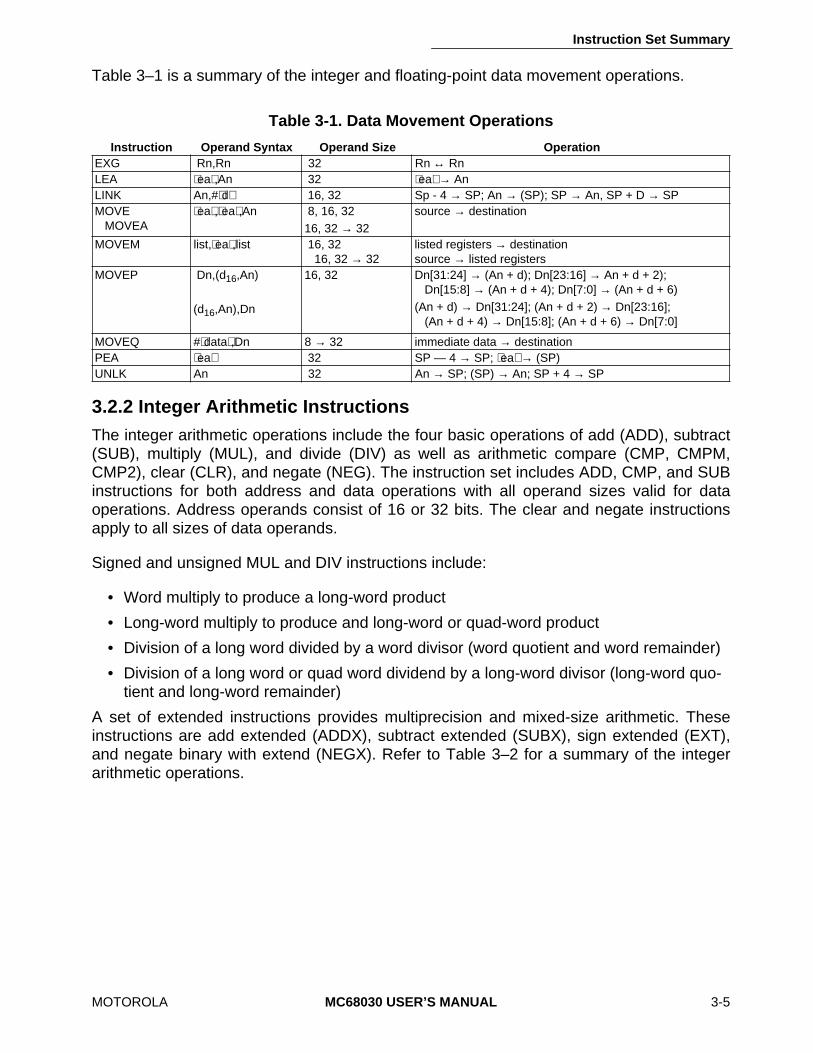
Instruction Set Summary
MOTOROLA
MC68030 USER’S MANUAL
3-5
Table 3–1 is a summary of the integer and floating-point data movement operations.
3.2.2 Integer Arithmetic Instructions
The integer arithmetic operations include the four basic operations of add (ADD), subtract(SUB), multiply (MUL), and divide (DIV) as well as arithmetic compare (CMP, CMPM,CMP2), clear (CLR), and negate (NEG). The instruction set includes ADD, CMP, and SUBinstructions for both address and data operations with all operand sizes valid for dataoperations. Address operands consist of 16 or 32 bits. The clear and negate instructionsapply to all sizes of data operands.
Signed and unsigned MUL and DIV instructions include:
• Word multiply to produce a long-word product
• Long-word multiply to produce and long-word or quad-word product
• Division of a long word divided by a word divisor (word quotient and word remainder)
• Division of a long word or quad word dividend by a long-word divisor (long-word quo-tient and long-word remainder)
A set of extended instructions provides multiprecision and mixed-size arithmetic. Theseinstructions are add extended (ADDX), subtract extended (SUBX), sign extended (EXT),and negate binary with extend (NEGX). Refer to Table 3–2 for a summary of the integerarithmetic operations.
Table 3-1. Data Movement Operations
Instruction Operand Syntax Operand Size Operation
EXG Rn,Rn 32 Rn
↔
Rn LEA
⟨
ea
⟩
,An 32
⟨
ea
⟩
→
AnLINK An,#
⟨
d
⟩
16, 32 Sp - 4
→
SP; An
→
(SP); SP
→
An, SP + D
→
SPMOVE
MOVEA
⟨
ea
⟩
,
⟨
ea
⟩
,An 8, 16, 32 16, 32
→
32source
→
destination
MOVEM list,
⟨
ea
⟩
,list 16, 32 16, 32
→
32 listed registers
→
destination source
→
listed registers MOVEP
Dn,(d
16
,An)
(d
16
,An),Dn
16, 32
Dn[31:24]
→
(An + d); Dn[23:16]
→
An + d + 2);Dn[15:8]
→
(An + d + 4); Dn[7:0]
→
(An + d + 6)(An + d)
→
Dn[31:24]; (An + d + 2)
→
Dn[23:16];(An + d + 4)
→
Dn[15:8]; (An + d + 6)
→
Dn[7:0]
MOVEQ #
⟨
data
⟩
,Dn 8
→
32 immediate data
→
destinationPEA
⟨
ea
⟩
32 SP — 4
→
SP;
⟨
ea
⟩
→
(SP)UNLK An 32 An
→
SP; (SP)
→
An; SP + 4
→
SP
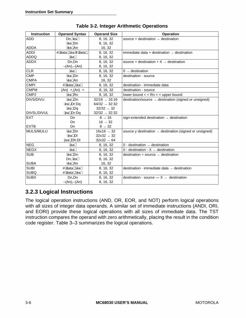
Instruction Set Summary
3-6
MC68030 USER’S MANUAL
MOTOROLA
3.2.3 Logical Instructions
The logical operation instructions (AND, OR, EOR, and NOT) perform logical operationswith all sizes of integer data operands. A similar set of immediate instructions (ANDI, ORI,and EORI) provide these logical operations with all sizes of immediate data. The TSTinstruction compares the operand with zero arithmetically, placing the result in the conditioncode register. Table 3–3 summarizes the logical operations.
Table 3-2. Integer Arithmetic Operations
Instruction Operand Syntax Operand Size Operation
ADD ADDA
Dn,
⟨
ea
⟩⟨
ea
⟩
,Dn
⟨
ea
⟩
,An
8, 16, 32 8, 16, 32 16, 32
source + destination
→
destination
ADDI ADDQ
#
⟨
data
⟩
,
⟨
ea
⟩
#
⟨
data
⟩
,
⟨
ea
⟩
8, 16, 32 8, 16, 32
immediate data + destination
→
destination
ADDX Dn,Dn
–(An),–(An) 8, 16, 32 8, 16, 32
source + destination + X
→
destination
CLR
⟨
ea
⟩
8, 16, 32 0
→
destination CMP CMPA
⟨
ea
⟩
,Dn
⟨
ea
⟩
,An 8, 16, 32 16, 32
destination - source
CMPI #
⟨
data
⟩
,
⟨
ea
⟩
8, 16, 32 destination - immediate data CMPM (An) +,(An) + 8, 16, 32 destination - sourceCMP2
⟨
ea
⟩
,Rn 8, 16, 32 lower bound < = Rn < = upper bound DIVS/DIVU
DIVSL/DIVUL
⟨
ea⟩,Dn⟨ea⟩,Dr:Dq
⟨ea⟩,Dq⟨ea⟩,Dr:Dq
32/16 → 16:1664/32 → 32:32
32/32 → 3232/32 → 32:32
destination/source → destination (signed or unsigned)
EXT
EXTB
Dn Dn Dn
8 → 1616 → 328 → 32
sign-extended destination → destination
MULS/MULU ⟨ea⟩,Dn⟨ea⟩,Dl
(ea⟩,Dh:Dl
16x16 → 3232x32 → 3232x32 → 64
source y destination → destination (signed or unsigned)
NEG ⟨ea⟩ 8, 16, 32 0 - destination → destinationNEGX ⟨ea⟩ 8, 16, 32 0 - destination - X → destinationSUB
SUBA
⟨ea⟩,DnDn,⟨ea⟩⟨ea⟩,An
8, 16, 32 8, 16, 32 16, 32
destination = source → destination
SUBI SUBQ
#⟨data⟩,⟨ea⟩#⟨data⟩,⟨ea⟩
8, 16, 32 8, 16, 32
destination - immediate data → destination
SUBX Dn,Dn –(An),–(An)
8, 16, 32 8, 16, 32
destination - source — X → destination

Instruction Set Summary
MOTOROLA MC68030 USER’S MANUAL 3-7
3.2.4 Shift and Rotate InstructionsThe arithmetic shift instructions (ASR and ASL) and logical shift instructions (LSR and LSL)provide shift operations in both directions. The ROR, ROL, ROXR, and ROXL instructionsperform rotate (circular shift) operations, with and without the extend bit. All shift and rotateoperations can be performed on either registers or memory.
Register shift and rotate operations shift all operand sizes. The shift count may be specifiedin the instruction operation word (to shift from 1–8 places) or in a register (modulo 64 shiftcount).
Memory shift and rotate operations shift word-length operands one bit position only. TheSWAP instruction exchanges the 16-bit halves of a register. Performance of shift/rotateinstructions is enhanced so that use of the ROR and ROL instructions with a shift count ofeight allows fast byte swapping. Table 3–4 is a summary of the shift and rotate operations.
Table 3-3. Logical Operations
Instruction Operand Syntax Operand Size OperationAND ⟨ea⟩,Dn
Dn,⟨ea⟩ 8, 16, 32 8, 16, 32
source Λ destination → destination
ANDI #⟨data⟩,⟨ea⟩ 8, 16, 32 immediate data Λ destination → destinationEOR Dn,⟨data⟩,⟨ea⟩ 8, 16, 32 source ⊕ destination → destinationEORI #⟨data⟩,⟨ea⟩ 8, 16, 32 immediate data x destination → destination NOT ⟨ea⟩ 8, 16, 32 ∼ destination → destinationOR ⟨ea⟩,Dn
Dn,⟨ea⟩ 8, 16, 32 8, 16, 32
source V destination → destination
ORI #⟨data⟩,⟨ea⟩ 8, 16, 32 immediate data V destination → destinationTST #⟨ea⟩ 8, 16, 32 source — 0 to set condition codes
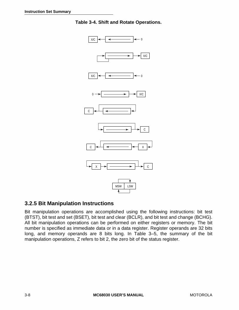
Instruction Set Summary
3-8 MC68030 USER’S MANUAL MOTOROLA
Table 3-4. Shift and Rotate Operations.
3.2.5 Bit Manipulation InstructionsBit manipulation operations are accomplished using the following instructions: bit test(BTST), bit test and set (BSET), bit test and clear (BCLR), and bit test and change (BCHG).All bit manipulation operations can be performed on either registers or memory. The bitnumber is specified as immediate data or in a data register. Register operands are 32 bitslong, and memory operands are 8 bits long. In Table 3–5, the summary of the bitmanipulation operations, Z refers to bit 2, the zero bit of the status register.
X/C
X/C 0
X/C0
C
C
XC
X/C 0
X C
MSW LSW
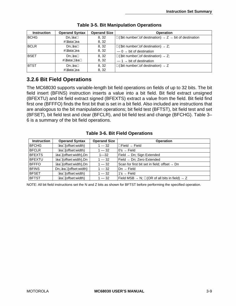
Instruction Set Summary
MOTOROLA MC68030 USER’S MANUAL 3-9
3.2.6 Bit Field OperationsThe MC68030 supports variable-length bit field operations on fields of up to 32 bits. The bitfield insert (BFINS) instruction inserts a value into a bit field. Bit field extract unsigned(BFEXTU) and bit field extract signed (BFEXTS) extract a value from the field. Bit field findfirst one (BFFFO) finds the first bit that is set in a bit field. Also included are instructions thatare analogous to the bit manipulation operations; bit field test (BFTST), bit field test and set(BFSET), bit field test and clear (BFCLR), and bit field test and change (BFCHG). Table 3–6 is a summary of the bit field operations.
NOTE: All bit field instructions set the N and Z bits as shown for BFTST before performing the specified operation.
Table 3-5. Bit Manipulation Operations
Instruction Operand Syntax Operand Size Operation BCHG Dn,⟨ea⟩
#⟨data⟩,ea 8, 32 8, 32
∼ (⟨bit number⟩ of destination) → Z → bit of destination
BCLR Dn,⟨ea⟩ #⟨data⟩,ea
8, 32 8, 32
∼ (⟨bit number⟩ of destination) → Z; — 0 → bit of destination
BSET Dn,⟨ea⟩ #⟨data⟩,⟨ea⟩
8, 32 8, 32
∼ (⟨bit number⟩ of destination) → Z; — 1 → bit of destination
BTST Dn,⟨ea⟩ #⟨data⟩,ea
8, 32 8, 32
∼ (⟨bit number⟩ of destination) → Z
Table 3-6. Bit Field Operations
Instruction Operand Syntax Operand Size OperationBFCHG ⟨ea⟩ {offset:width} 1 — 32 ∼ Field → FieldBFCLR ⟨ea⟩ {offset:width} 1 — 32 0's → FieldBFEXTS ⟨ea⟩ {offset:width},Dn 1—32 Field → Dn; Sign ExtendedBFEXTU ⟨ea⟩ {offset:width},Dn 1 — 32 Field → Dn; Zero ExtendedBFFFO ⟨ea⟩ {offset:width},Dn 1 — 32 Scan for first bit set in field; offset → DnBFINS Dn,⟨ea⟩ {offset:width} 1 — 32 Dn → FieldBFSET ⟨ea⟩ {offset:width} 1 — 32 1's → FieldBFTST ⟨ea⟩ {offset:width} 1 — 32 Field MSB → N; ∼ (OR of all bits in field) → Z
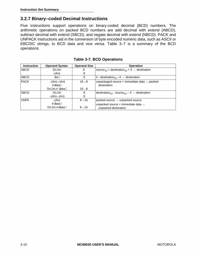
Instruction Set Summary
3-10 MC68030 USER’S MANUAL MOTOROLA
3.2.7 Binary–coded Decimal InstructionsFive instructions support operations on binary-coded decimal (BCD) numbers. Thearithmetic operations on packed BCD numbers are add decimal with extend (ABCD),subtract decimal with extend (SBCD), and negate decimal with extend (NBCD). PACK andUNPACK instructions aid in the conversion of byte encoded numeric data, such as ASCII orEBCDIC strings, to BCD data and vice versa. Table 3–7 is a summary of the BCDoperations.
Table 3-7. BCD Operations
Instruction Operand Syntax Operand Size OperationABCD Dn,Dn
–(An)8 8
source10 + destination10 + X → destination
NBCD ⟨ea⟩ 8 0 - destination10 –X → destination
PACK –(An),–(An) #⟨data⟩
Dn,Dn,# ⟨data⟩
16→8
16→8
unpackaged source + immediate data → packeddestination
SBCD Dn,Dn –(An),–(An)
8 8
destination10 - source10 – X → destination
UNPK –(An)#⟨data⟩
Dn,Dn,#⟨data⟩
8→16
8→16
packed source → unpacked sourceunpacked source + immediate data →
unpacked destination

Instruction Set Summary
MOTOROLA MC68030 USER’S MANUAL 3-11
3.2.8 Program Control InstructionsA set of subroutine call and return instructions and conditional and unconditional branchinstructions perform program control operations. The no operation instruction (NOP) may beused to force synchronization of the internal pipelines. Table 3–8 summarizes theseinstructions.
Letters cc in the integer instruction mnemonics Bcc, DBcc, and Scc specify testing one of the following conditions:CC — Carry clear GE — Greater or equalLS — Lower or same PL — PlusCS — Carry set GT — Greater thanLT — Less than T — Always true*EQ — Equal HI — HigherMI — Minus VC — Overflow clearF — Never true* LE — -Less or equalNE — Not equal VS — Overflow set*Not applicable to the Bcc instructions.
Table 3-8. Program Control Operations
Instruction Operand Syntax Operand Size OperationInteger and Floating-Point Conditional
Bcc ⟨ label⟩ 8, 16, 32 if condition true, then PC + d → PC DBcc Dn,⟨ label⟩ 16 if condition false, then Dn — 1 → Dn
if Dn ≠ -1, then PC + d → PCScc ⟨ea⟩ 8 if condition true, then 1's → destination;
else 0's → destinationUnconditional
BRA ⟨ label⟩ 8, 16, 32 PC + d → PCBSR ⟨ label⟩ 8, 16, 32 SP — 4 → SP; PC→(SP); PC + d → PCJMP ⟨ea⟩ none destination → PCJSR ⟨ea⟩ none SP — 4 → SP; PC→ (SP); destination → PCNOP none none PC + 2 → PC
ReturnsRTD #⟨d⟩ 16 (SP) → PC; SP + 4 + d → SPRTR none none (SP) → CCR; SP + 2 → SP; (SP) → PC; SP + 4 → SPRTS none none (SP) → PC; SP + 4→ SP
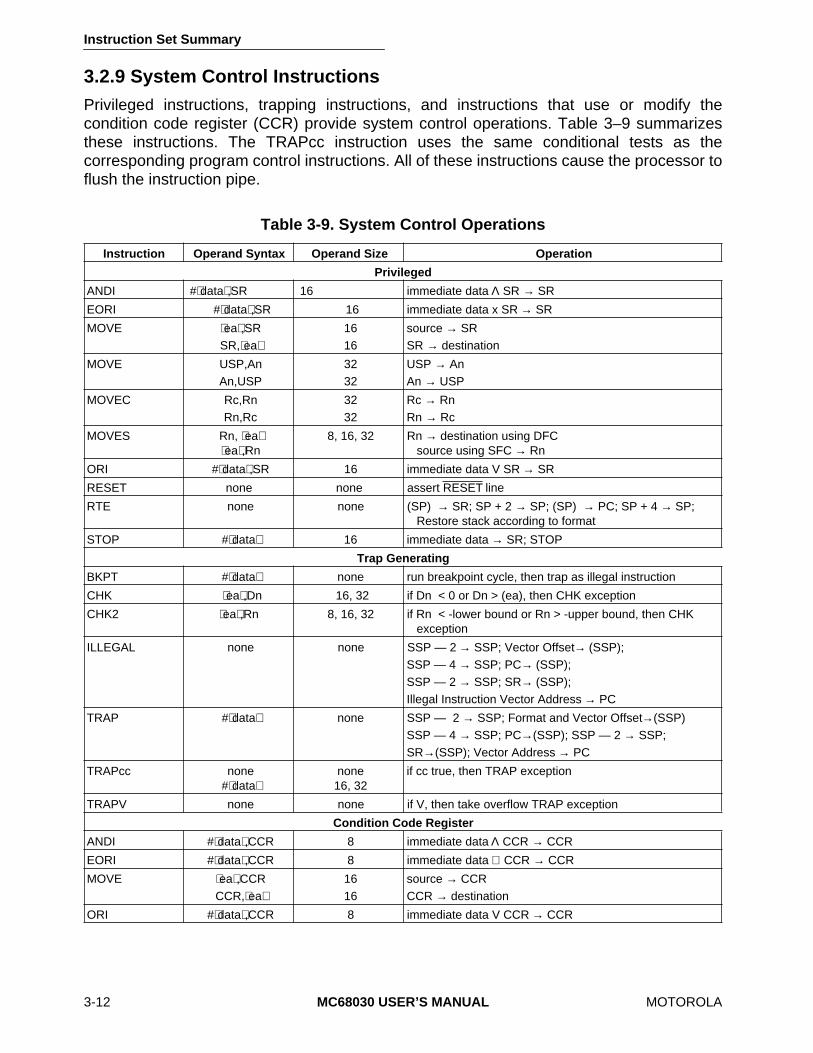
Instruction Set Summary
3-12 MC68030 USER’S MANUAL MOTOROLA
3.2.9 System Control InstructionsPrivileged instructions, trapping instructions, and instructions that use or modify thecondition code register (CCR) provide system control operations. Table 3–9 summarizesthese instructions. The TRAPcc instruction uses the same conditional tests as thecorresponding program control instructions. All of these instructions cause the processor toflush the instruction pipe.
Table 3-9. System Control Operations
Instruction Operand Syntax Operand Size Operation
Privileged
ANDI #⟨data⟩,SR 16 immediate data Λ SR → SR
EORI #⟨data⟩,SR 16 immediate data x SR → SR
MOVE ⟨ea⟩,SR SR,⟨ea⟩
16 16
source → SRSR → destination
MOVE USP,An An,USP
32 32
USP → AnAn → USP
MOVEC Rc,Rn Rn,Rc
32 32
Rc → RnRn → Rc
MOVES Rn, ⟨ea⟩ ⟨ea⟩,Rn
8, 16, 32 Rn → destination using DFCsource using SFC → Rn
ORI #⟨data⟩,SR 16 immediate data V SR → SR
RESET none none assert RESET line
RTE none none (SP) → SR; SP + 2 → SP; (SP) → PC; SP + 4 → SP;Restore stack according to format
STOP #⟨data⟩ 16 immediate data → SR; STOP
Trap Generating
BKPT #⟨data⟩ none run breakpoint cycle, then trap as illegal instruction
CHK ⟨ea⟩,Dn 16, 32 if Dn < 0 or Dn > (ea), then CHK exception
CHK2 ⟨ea⟩,Rn 8, 16, 32 if Rn < -lower bound or Rn > -upper bound, then CHK exception
ILLEGAL none none SSP — 2 → SSP; Vector Offset→ (SSP);SSP — 4 → SSP; PC→ (SSP);SSP — 2 → SSP; SR→ (SSP);Illegal Instruction Vector Address → PC
TRAP #⟨data⟩ none SSP — 2 → SSP; Format and Vector Offset→(SSP)SSP — 4 → SSP; PC→(SSP); SSP — 2 → SSP;SR→(SSP); Vector Address → PC
TRAPcc none #⟨data⟩
none 16, 32
if cc true, then TRAP exception
TRAPV none none if V, then take overflow TRAP exception
Condition Code Register
ANDI #⟨data⟩,CCR 8 immediate data Λ CCR → CCR
EORI #⟨data⟩,CCR 8 immediate data ⊕ CCR → CCR
MOVE ⟨ea⟩,CCR CCR,⟨ea⟩
16 16
source → CCRCCR → destination
ORI #⟨data⟩,CCR 8 immediate data V CCR → CCR
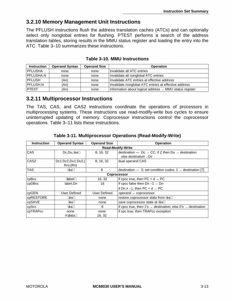
Instruction Set Summary
MOTOROLA MC68030 USER’S MANUAL 3-13
3.2.10 Memory Management Unit InstructionsThe PFLUSH instructions flush the address translation caches (ATCs) and can optionallyselect only nonglobal entries for flushing. PTEST performs a search of the addresstranslation tables, storing results in the MMU status register and loading the entry into theATC. Table 3–10 summarizes these instructions.
3.2.11 Multiprocessor InstructionsThe TAS, CAS, and CAS2 instructions coordinate the operations of processors inmultiprocessing systems. These instructions use read-modify-write bus cycles to ensureuninterrupted updating of memory. Coprocessor instructions control the coprocessoroperations. Table 3–11 lists these instructions.
Table 3-10. MMU Instructions
Instruction Operand Syntax Operand Size OperationPFLUSHA none none Invalidate all ATC entriesPFLUSHA.N none none Invalidate all nonglobal ATC entriesPFLUSH (An) none Invalidate ATC entries at effective addressPFLUSH.N (An) none Invalidate nonglobal ATC entries at effective addressPTEST (An) none Information about logical address → MMU status register
Table 3-11. Multiprocessor Operations (Read-Modify-Write)
Instruction Operand Syntax Operand Size OperationRead-Modify-Write
CAS Dc,Du,⟨ea⟩ 8, 16, 32 destination — Dc → CC; if Z then Du → destinationelse destination→Dc
CAS2 Dc1:Dc2,Du1:Du2,(Rn):(Rn)
8, 16, 32 dual operand CAS
TAS ⟨ea⟩ 8 destination — 0; set condition codes; 1 → destination [7]Coprocessor
cpBcc ⟨ label⟩ 16, 32 if cpcc true, then PC + d → PCcpDBcc label,Dn 16 if cpcc false then Dn –1 → Dn
if Dn ≠ –1, then PC + d → PCcpGEN User Defined User Defined operand → coprocessorcpRESTORE ⟨ea⟩ none restore coprocessor state from ⟨ea⟩cpSAVE ⟨ea⟩ none save coprocessor state at ⟨ea⟩cpScc ⟨ea⟩ 8 if cpcc true, then 1's → destination; else 0's → destinationcpTRAPcc none
#⟨data⟩ none16, 32
if cpc true, then TRAPcc exception

Instruction Set Summary
3-14 MC68030 USER’S MANUAL MOTOROLA
3.3 INTEGER CONDITION CODESThe CCR portion of the SR contains five bits which indicate the results of many integerinstructions. Program and system control instructions use certain combinations of these bitsto control program and system flow.
The first four bits represent a condition resulting from a processor operation. The X bit is anoperand for multiprecision computations; when it is used, it is set to the value of the C bit.The carry bit and the multiprecision extend bit are separate in the M68000 Family to simplifyprogramming techniques that use them (refer to Table 3–8 as an example).
The condition codes were developed to meet two criteria:
• Consistency across instructions, uses, and instances
• Meaningful Results no change unless it provides useful information
Consistency across instructions means that all instructions that are special cases of moregeneral instructions affect the condition codes in the same way. Consistency acrossinstances means that all instances of an instruction affect the condition codes in the sameway. Consistency across uses means that conditional instructions test the condition codessimilarly and provide the same results, regardless of whether the condition codes are set bya compare, test, or move instruction.
In the instruction set definitions, the CCR is shown as follows:
where:
X (extend)
Set to the value of the C bit for arithmetic operations. Otherwise not affected or set toa specified result.
N (negative)
Set if the most significant bit of the result is set. Cleared otherwise.
Z (zero)
Set if the result equals zero. Cleared otherwise.
V (overflow)
Set if arithmetic overflow occurs. This implies that the result cannot be represented inthe operand size. Cleared otherwise.
C (carry)
Set if a carry out of the most significant bit of the operand occurs for an addition. Alsoset if a borrow occurs in a subtraction. Cleared otherwise.
X N Z V C

Instruction Set Summary
MOTOROLA MC68030 USER’S MANUAL 3-15
3.3.1 Condition Code ComputationMost operations take a source operand and a destination operand, compute, and store theresult in the destination location. Single-operand operations take a destination operand,compute, and store the result in the destination location. Table 3–12 lists each instructionand how it affects the condition code bits.
Table 3-12. Condition Code Computations (Sheet 1 of 2)
Operations X N Z V C Special Definition
ABCD * U ? U ? C =-Decimal CarryZ =-Z Λ Rm Λ . . . Λ R0
ADD, ADDI, ADDQ * * * ? ? V = Sm Λ Dm Λ Rm V Sm Λ Dm Λ RmC = Sm Λ Dm V Rm Λ Dm V Sm Λ Rm
ADDX * * ? ? ? V = Sm Λ Dm Λ Rm V Sm Λ Dm Λ RmC = Sm Λ Dm V Rm Λ Dm V Sm Λ Rm Z = Z Λ Rm Λ . . . Λ R0
AND, ANDI, EOR, EORI,MOVEQ, MOVE, OR, ORICLR, EXT, NOT, TAS, TST
— * * 0 0
CHK — * U U U
CHK2, CMP2 — U ? U ? Z = (R = LB) V (R = UB)C = (LB < = UB) Λ (IR < LB) V (R > UB))V = (UB <LB) Λ (R >UB) Λ (R <LB)
SUB, SUBI, SUBQ * * * ? ? V = Sm Λ Dm Λ Rm V Sm Λ Dm Λ RmC = Sm Λ Dm V Rm Λ Dm V Sm Λ Rm
SUBX * * ? ? ? V = Sm Λ Dm Λ Rm V Sm Λ Dm Λ RmC = Sm Λ Dm V Rm Λ Dm V Sm Λ RmZ = Z Λ Rm Λ . . . Λ R0
CAS, CAS2, CMP, CMPI,CMPM
— * * ? ? V = Sm Λ Dm Λ Rm V Sm Λ Dm Λ RmC = Sm Λ Dm V Rm Λ Dm V Sm Λ Rm
DIVS, DUVI — * * ? 0 V = Division Overflow
MULS, MULU — * * ? 0 V = Multiplication Overflow
SBCD, NBCD * U U ? C = Decimal BorrowZ = Z Λ Rm Λ . . . Λ R0
NEG * * * ? ? V = Dm Λ RmC = Dm V Rm
NEGX * * ? ? ? V = Dm Λ RmC = Dm V RmZ = Z Λ Rm Λ . . . Λ R0
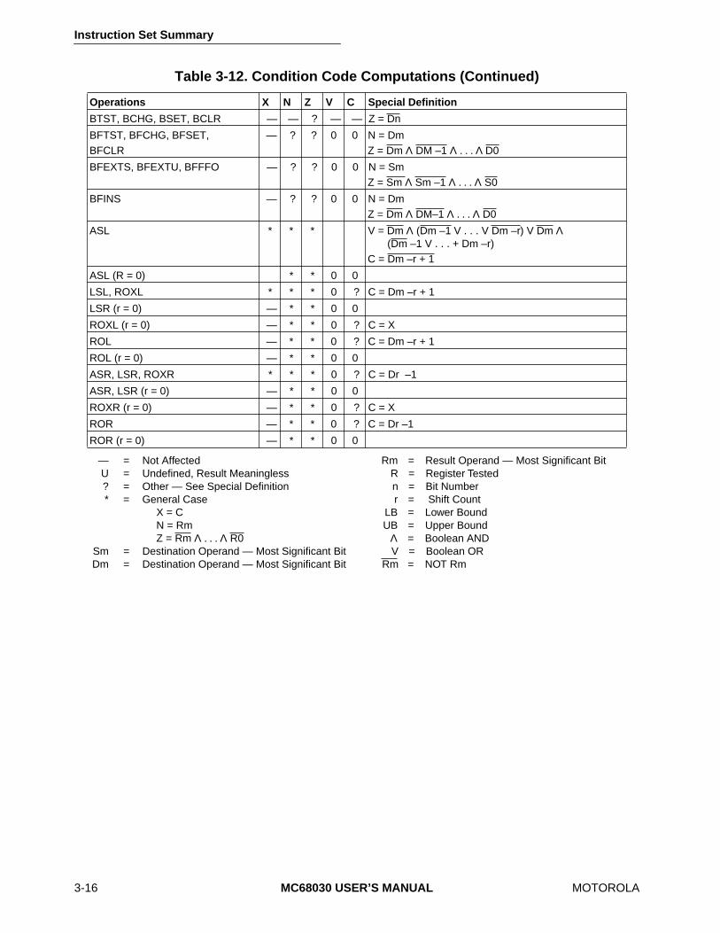
Instruction Set Summary
3-16 MC68030 USER’S MANUAL MOTOROLA
— = Not Affected Rm = Result Operand — Most Significant BitU = Undefined, Result Meaningless R = Register Tested? = Other — See Special Definition n = Bit Number* = General Case r = Shift Count
X = C LB = Lower BoundN = Rm UB = Upper BoundZ = Rm Λ . . . Λ R0 Λ = Boolean AND
Sm = Destination Operand — Most Significant Bit V = Boolean ORDm = Destination Operand — Most Significant Bit Rm = NOT Rm
Table 3-12. Condition Code Computations (Continued)
Operations X N Z V C Special Definition
BTST, BCHG, BSET, BCLR — — ? — — Z = Dn
BFTST, BFCHG, BFSET,BFCLR
— ? ? 0 0 N = DmZ = Dm Λ DM –1 Λ . . . Λ D0
BFEXTS, BFEXTU, BFFFO — ? ? 0 0 N = SmZ = Sm Λ Sm –1 Λ . . . Λ S0
BFINS — ? ? 0 0 N = DmZ = Dm Λ DM–1 Λ . . . Λ D0
ASL * * * V = Dm Λ (Dm –1 V . . . V Dm –r) V Dm Λ(Dm –1 V . . . + Dm –r)
C = Dm –r + 1
ASL (R = 0) * * 0 0
LSL, ROXL * * * 0 ? C = Dm –r + 1
LSR (r = 0) — * * 0 0
ROXL (r = 0) — * * 0 ? C = X
ROL — * * 0 ? C = Dm –r + 1
ROL (r = 0) — * * 0 0
ASR, LSR, ROXR * * * 0 ? C = Dr –1
ASR, LSR (r = 0) — * * 0 0
ROXR (r = 0) — * * 0 ? C = X
ROR — * * 0 ? C = Dr –1
ROR (r = 0) — * * 0 0
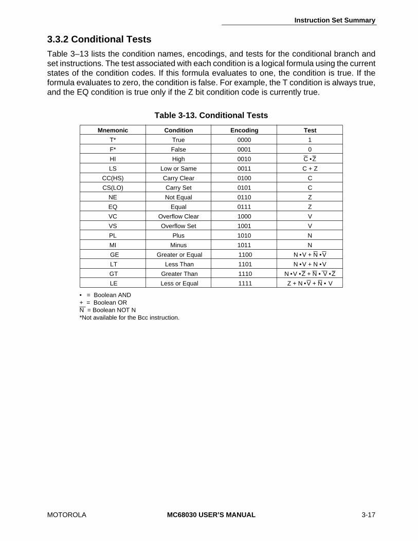
Instruction Set Summary
MOTOROLA MC68030 USER’S MANUAL 3-17
3.3.2 Conditional TestsTable 3–13 lists the condition names, encodings, and tests for the conditional branch andset instructions. The test associated with each condition is a logical formula using the currentstates of the condition codes. If this formula evaluates to one, the condition is true. If theformula evaluates to zero, the condition is false. For example, the T condition is always true,and the EQ condition is true only if the Z bit condition code is currently true.
• = Boolean AND+ = Boolean ORN = Boolean NOT N*Not available for the Bcc instruction.
Table 3-13. Conditional Tests
Mnemonic Condition Encoding Test
T* True 0000 1
F* False 0001 0
HI High 0010 C •Z
LS Low or Same 0011 C + Z
CC(HS) Carry Clear 0100 C
CS(LO) Carry Set 0101 C
NE Not Equal 0110 Z
EQ Equal 0111 Z
VC Overflow Clear 1000 V
VS Overflow Set 1001 V
PL Plus 1010 N
MI Minus 1011 N
GE Greater or Equal 1100 N •V + N •V
LT Less Than 1101 N •V + N •V
GT Greater Than 1110 N •V •Z + N • V •Z
LE Less or Equal 1111 Z + N •V + N • V
Instruction Set Summary
3-18 MC68030 USER’S MANUAL MOTOROLA
3.4 INSTRUCTION SET SUMMARYTable 3–14 provides a alphabetized listing of the MC68030 instruction set listed by opcode,operation, and syntax.
Table 3–14 use notational conventions for the operands, the subfields and qualifiers, andthe operations performed by the instructions. In the syntax descriptions, the left operand isthe source operand, and the right operand is the destination operand. The following listcontains the notations used in Table 3–14.
Notation for operands:
PC — Program counter
SR — Status register
V — Overflow condition code
Immediate Data — Immediate data from the instruction
Source — Source contents
Destination — Destination contents
Vector — Location of exception vector
+ inf — Positive infinity
–inf — Negative infinity
⟨fmt⟩ — Operand data format: byte (B) word (W), long(L), single (S), double (D), extended (X), or packed (P)
FPm — One of eight floating-point data registers (alwaysspecifies the source register)
FPn — One of eight floating-point data registers (alwaysspecifies the destination register)
Notation for subfields and qualifiers:
⟨bit⟩ of (operand⟩ — Selects a single bit of the operand
⟨ea⟩ {offset:width} — Selects a bit field
(⟨operand⟩) — The contents of the referenced location
⟨operand⟩ 10 — The operand is binary-coded decimal; operations are per-formed in decimal
(⟨address register⟩) — The register indirect operation
–(⟨address register⟩) — Indicates that the operand register points to the memory
(⟨address register⟩) + — Location of the instruction operand — the optional modequalifiers are -, +, (d), and (d,ix)
#xxx or #⟨data⟩ — Immediate data that follows the instruction word(s)
Instruction Set Summary
MOTOROLA MC68030 USER’S MANUAL 3-19
Notations for operations that have two operands, written ⟨operand⟩ ⟨op⟩ ⟨operand⟩ , where⟨op⟩ is one of the following:
→ — The source operand is moved to the destination operand
↔ — The two operands are exchanged
+ — The operands are added
– — The destination operand is subtracted from the sourceoperand
x — The operands are multiplied
÷ — The source operand is divided by the destination operand
< — Relational test, true if source operand is less than destina-tion operand
> — Relational test, true if source operand is greater than des-tination operand
V — Logical OR
⊕ — Logical exclusive OR
Λ — Logical AND
shifted by, rotated by — The source operand is shifted or rotated by the number ofpositions specified by the second operand
Notation for single-operand operations:~⟨operand⟩ — The operand is logically complemented
⟨operand⟩ sign-extended— The operand is sign extended; all bits of the upper portionare made equal to the high-order bit of the lower portion
⟨operand⟩ tested — The operand is compared to zero and the condition codesare set appropriately
Notation for other operations:TRAP — Equivalent to Format/Offset Word→ (SSP); SSP –2
→ SSP; PC→ (SSP); SSP – 4 → SSP; SR→ (SSP); SSP–2 → SSP; (vector) → PC
STOP — Enter the stopped state, waiting for the interrupts
If ⟨condition⟩ then — The condition is tested. If true, the operations
⟨operations⟩ else — after "then'' are performed. If the condition is
⟨operations⟩ — false and the optional "else'' clause is present, the opera-tions after "else" are performed. If the condition is false andelse is omitted, the instruction performs no operation. Referto the Bcc instruction description as an example.
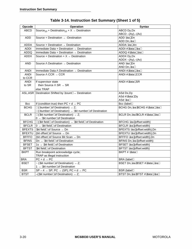
Instruction Set Summary
3-20 MC68030 USER’S MANUAL MOTOROLA
Table 3-14. Instruction Set Summary (Sheet 1 of 5)
Opcode Operation Syntax ABCD Source10 + Destination10 + X → Destination ABCD Dy,Dx
ABCD –(Ay),–(Ax) ADD Source + Destination → -Destination ADD ⟨ea⟩,Dn
ADD Dn,⟨ea⟩ ADDA Source + Destination → Destination ADDA ⟨ea⟩,An ADDI Immediate Data + Destination → Destination ADDI #⟨data⟩,⟨ea⟩ ADDQ Immediate Data + Destination → Destination ADDQ #⟨data⟩,⟨ea⟩ ADDX Source + Destination + X → Destination ADDX Dy,Dx
ADDX –(Ay),–(Ax) AND Source Λ Destination → Destination AND ⟨ea⟩,Dn
AND Dn,⟨ea⟩ ANDI Immediate Data Λ Destination → Destination ANDI #⟨data⟩,⟨ea⟩ ANDI
to CCRSource Λ CCR → CCR ANDI #⟨data⟩,CCR
ANDI to SR
If supervisor state then Source Λ SR → SR
else TRAP
ANDI #⟨data⟩,SR
ASL,ASR Destination Shifted by ⟨count⟩ → Destination ASd Dx,Dy ASd #⟨data⟩,DyASd ⟨ea⟩
Bcc If (condition true) then PC + d → PC Bcc (label⟩ BCHG ∼ (⟨number⟩ of Destination) → Z;
∼ (⟨number⟩ of Destination) → ⟨bit number⟩ of DestinationBCHG Dn,⟨ea⟩BCHG #⟨data⟩,⟨ea⟩
BCLR ∼ (⟨bit number⟩ of Destination) → Z;0 → ⟨bit number⟩ of Destination
BCLR Dn,⟨ea⟩BCLR #⟨data⟩,⟨ea⟩
BFCHG ∼ (⟨bit field⟩ of Destination) → ⟨bit field⟩ of Destination BFCHG ⟨ea⟩{offset:width} BFCLR 0 → ⟨bit field⟩ of Destination BFCLR ⟨ea⟩{offset:width}BFEXTS ⟨bit field⟩ of Source → Dn BFEXTS ⟨ea⟩{offset:width},DnBFEXTU (bit offset⟩ of Source → Dn BFEXTU ⟨ea⟩{offset:width},DnBFFFO (bit offset⟩ of Source Bit Scan → Dn BFFFO ⟨ea⟩{offset:width},DnBFINS Dn → ⟨bit field⟩ of Destination BFINS Dn,⟨ea⟩{offset:width}BFSET 1s → ⟨bit field⟩ of Destination BFSET ⟨ea⟩{offset:width}BFTST ⟨bit field⟩ of Destination BFTST ⟨ea⟩{offset:width}
BKPT Run breakpoint acknowledge cycle; TRAP as illegal instruction
BKPT # ⟨data⟩
BRA PC + d → PC BRA (label⟩ BSET ~ (⟨bit number⟩ of Destination) → Z;
1 → ⟨bit number⟩ of DestinationBSET Dn,⟨ea⟩BSET #⟨data⟩,⟨ea⟩
BSR SP – 4 → SP; PC → (SP); PC + d → PC BSR (label⟩ BTST –(⟨bit number⟩ of Destination) → Z; BTST Dn,⟨ea⟩BTST #⟨data⟩,⟨ea⟩
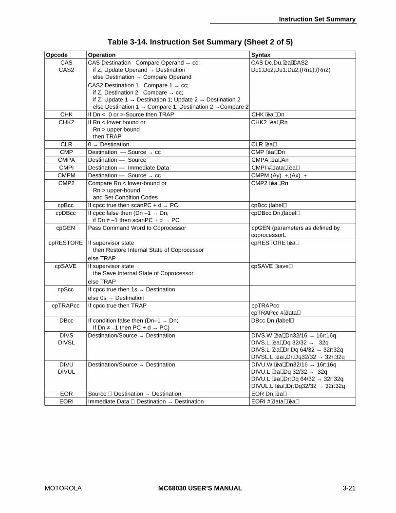
Instruction Set Summary
MOTOROLA MC68030 USER’S MANUAL 3-21
Table 3-14. Instruction Set Summary (Sheet 2 of 5)
Opcode Operation Syntax CAS CAS2
CAS Destination Compare Operand → cc; if Z, Update Operand → Destination else Destination → Compare Operand
CAS2 Destination 1 Compare 1 → cc; if Z, Destination 2 Compare → cc; if Z, Update 1 → Destination 1; Update 2 → Destination 2else Destination 1 → Compare 1; Destination 2 →Compare 2
CAS Dc,Du,⟨ea⟩CAS2 Dc1:Dc2,Du1:Du2,(Rn1):(Rn2)
CHK If Dn < 0 or >-Source then TRAP CHK ⟨ea⟩,Dn CHK2 If Rn < lower bound or
Rn > upper bound then TRAP
CHK2 ⟨ea⟩,Rn
CLR 0 → Destination CLR ⟨ea⟩ CMP Destination — Source → cc CMP ⟨ea⟩,Dn
CMPA Destination — Source CMPA ⟨ea⟩,An CMPI Destination — Immediate Data CMPI #⟨data⟩,⟨ea⟩ CMPM Destination — Source → cc CMPM (Ay) +,(Ax) + CMP2 Compare Rn < lower-bound or
Rn > upper-bound and Set Condition Codes
CMP2 ⟨ea⟩,Rn
cpBcc If cpcc true then scanPC + d → PC cpBcc (label⟩cpDBcc If cpcc false then (Dn –1 → Dn;
if Dn ≠ –1 then scanPC + d → PCcpDBcc Dn,(label⟩
cpGEN Pass Command Word to Coprocessor cpGEN (parameters as defined bycoprocessorL
cpRESTORE If supervisor statethen Restore Internal State of Coprocessor
else TRAP
cpRESTORE ⟨ea⟩
cpSAVE If supervisor statethe Save Internal State of Coprocessor
else TRAP
cpSAVE ⟨save⟩
cpScc If cpcc true then 1s → Destinationelse 0s → Destination
cpTRAPcc If cpcc true then TRAP cpTRAPcccpTRAPcc #⟨data⟩
DBcc If condition false then (Dn–1 → Dn;If Dn ≠ –1 then PC + d → PC)
DBcc Dn,(label⟩
DIVS DIVSL
Destination/Source → Destination DIVS.W ⟨ea⟩,Dn32/16 → 16r:16qDIVS.L ⟨ea⟩,Dq 32/32 → 32qDIVS.L ⟨ea⟩,Dr:Dq 64/32 → 32r:32qDIVSL.L ⟨ea⟩,Dr:Dq32/32 → 32r:32q
DIVU DIVUL
Destination/Source → Destination DIVU.W ⟨ea⟩,Dn32/16 → 16r:16qDIVU.L ⟨ea⟩,Dq 32/32 → 32qDIVU.L ⟨ea⟩,Dr:Dq 64/32 → 32r:32qDIVUL.L ⟨ea⟩,Dr:Dq32/32 → 32r:32q
EOR Source ⊕ Destination → Destination EOR Dn,⟨ea⟩ EORI Immediate Data ⊕ Destination → Destination EORI #⟨data⟩,⟨ea⟩
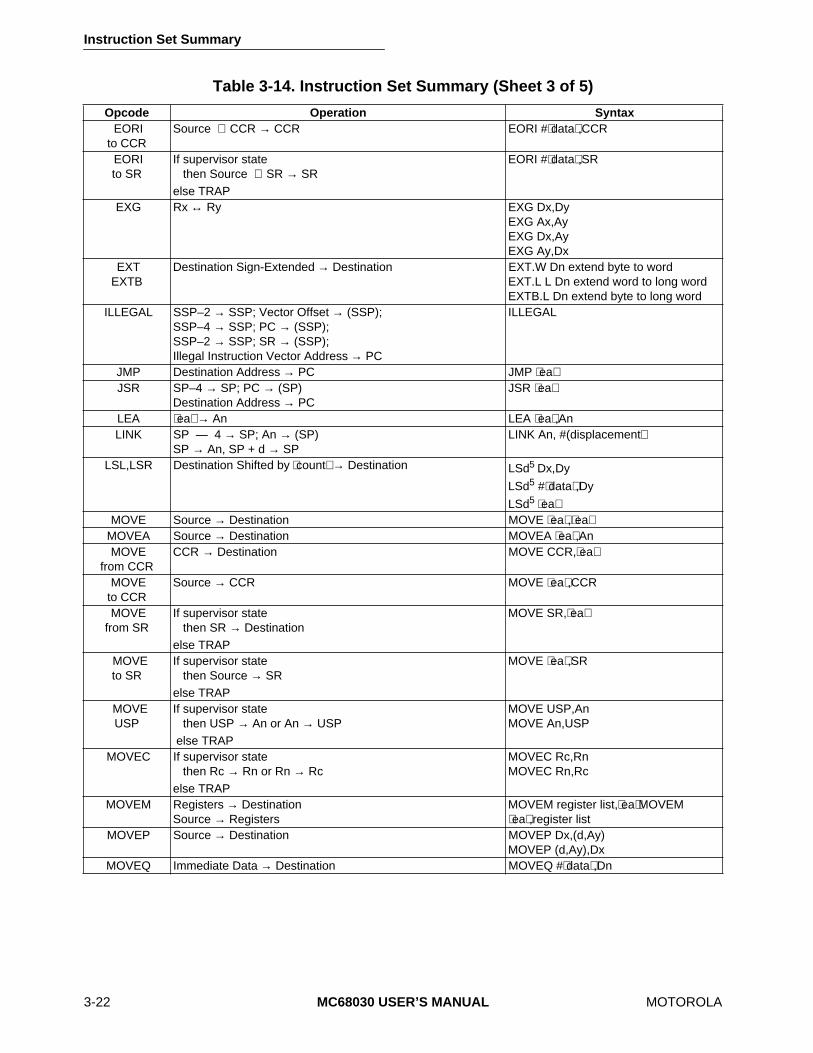
Instruction Set Summary
3-22 MC68030 USER’S MANUAL MOTOROLA
Table 3-14. Instruction Set Summary (Sheet 3 of 5)
Opcode Operation Syntax EORI to CCR
Source ⊕ CCR → CCR EORI #⟨data⟩,CCR
EORI to SR
If supervisor state then Source ⊕ SR → SR
else TRAP
EORI #⟨data⟩,SR
EXG Rx ↔ Ry EXG Dx,Dy EXG Ax,Ay EXG Dx,Ay EXG Ay,Dx
EXT EXTB
Destination Sign-Extended → Destination EXT.W Dn extend byte to word EXT.L L Dn extend word to long wordEXTB.L Dn extend byte to long word
ILLEGAL SSP–2 → SSP; Vector Offset → (SSP);SSP–4 → SSP; PC → (SSP);SSP–2 → SSP; SR → (SSP);Illegal Instruction Vector Address → PC
ILLEGAL
JMP Destination Address → PC JMP ⟨ea⟩ JSR SP–4 → SP; PC → (SP)
Destination Address → PCJSR ⟨ea⟩
LEA ⟨ea⟩ → An LEA ⟨ea⟩,An LINK SP — 4 → SP; An → (SP)
SP → An, SP + d → SPLINK An, #(displacement⟩
LSL,LSR Destination Shifted by ⟨count⟩ → Destination LSd5 Dx,Dy
LSd5 #⟨data⟩,Dy
LSd5 ⟨ea⟩ MOVE Source → Destination MOVE ⟨ea⟩,⟨ea⟩
MOVEA Source → Destination MOVEA ⟨ea⟩,An MOVE
from CCRCCR → Destination MOVE CCR,⟨ea⟩
MOVE to CCR
Source → CCR MOVE ⟨ea⟩,CCR
MOVE from SR
If supervisor state then SR → Destination
else TRAP
MOVE SR,⟨ea⟩
MOVE to SR
If supervisor state then Source → SR
else TRAP
MOVE ⟨ea⟩,SR
MOVE USP
If supervisor state then USP → An or An → USP
else TRAP
MOVE USP,An MOVE An,USP
MOVEC If supervisor state then Rc → Rn or Rn → Rc
else TRAP
MOVEC Rc,Rn MOVEC Rn,Rc
MOVEM Registers → DestinationSource → Registers
MOVEM register list,⟨ea⟩MOVEM ⟨ea⟩,register list
MOVEP Source → Destination MOVEP Dx,(d,Ay) MOVEP (d,Ay),Dx
MOVEQ Immediate Data → Destination MOVEQ #⟨data⟩,Dn

Instruction Set Summary
MOTOROLA MC68030 USER’S MANUAL 3-23
Table 3-14. Instruction Set Summary (Sheet 4 of 5)
Opcode Operation Syntax MOVES If supervisor state
then Rn → Destination [DFC] or Source [SFC] → Rnelse TRAP
MOVES Rn,⟨ea⟩MOVES ⟨ea⟩,Rn
MULS Source y-Destination → Destination MULS.W ⟨ea⟩,Dn 16 x 16 → 32MULS.L ⟨ea⟩,Dl 32 x 32 → 32MULS.L ⟨ea⟩,Dh:Dl 32 x 32 → 64
MULU Source y-Destination → Destination MULU.W ⟨ea⟩,Dn 16 x 16 → 32MULU.L ⟨ea⟩,Dl 32 x 32 → 32MULU.L ⟨ea⟩,Dh:Dl 32 x 32 → 64
NBCD 0 — (Destination10) — X → Destination NBCD ⟨ea⟩ NEG 0 — (Destination) → Destination NEG ⟨ea⟩
NEGX 0 — (Destination) — X → Destination NEGX ⟨ea⟩ NOP None NOP NOT ∼ Destination → Destination NOT ⟨ea⟩ OR Source V Destination → Destination OR ⟨ea⟩,Dn
OR Dn,⟨ea⟩ ORI Immediate Data V Destination → Destination ORI #⟨data⟩,⟨ea⟩ ORI
to CCRSource V CCR → CCR ORI #⟨data⟩,CCR
ORI to SR
If supervisor state then Source V SR → SR
else TRAP
ORI #⟨data⟩,SR
PACK Source (Unpacked BCD) + adjustment → Destintion (Packed BCD)
PACK –(Ax),–(Ay),#(adjustment⟩PACK Dx,Dy,#(adjustment⟩
PEA Sp –4 → SP; ⟨ea⟩ → (SP) PEA ⟨ea⟩PFLUSH If supervisor state
then invalidate instruction and data ATC entries for destination address
else TRAPPLOAD If supervisor state
then entry → ATCelse TRAP
PMOVE If supervisor statethen (Source) → MRn or MRn → (Destination)
PTEST If supervisor statethen logical address status → MMUSR; entry → ATC
else TRAP RESET If supervisor state
then Assert RSTO Line else TRAP
RESET
ROL,ROR Destination Rotated by ⟨count⟩ → Destination ROd5 Rx,Dy
ROd5 #⟨data⟩,Dy
ROd5 ⟨ea⟩ ROXL, ROXR
Destination Rotated with X by ⟨count⟩ → Destination ROXd5 Dx,Dy
ROXd5 #⟨data⟩,Dy
ROXd5 ⟨ea⟩
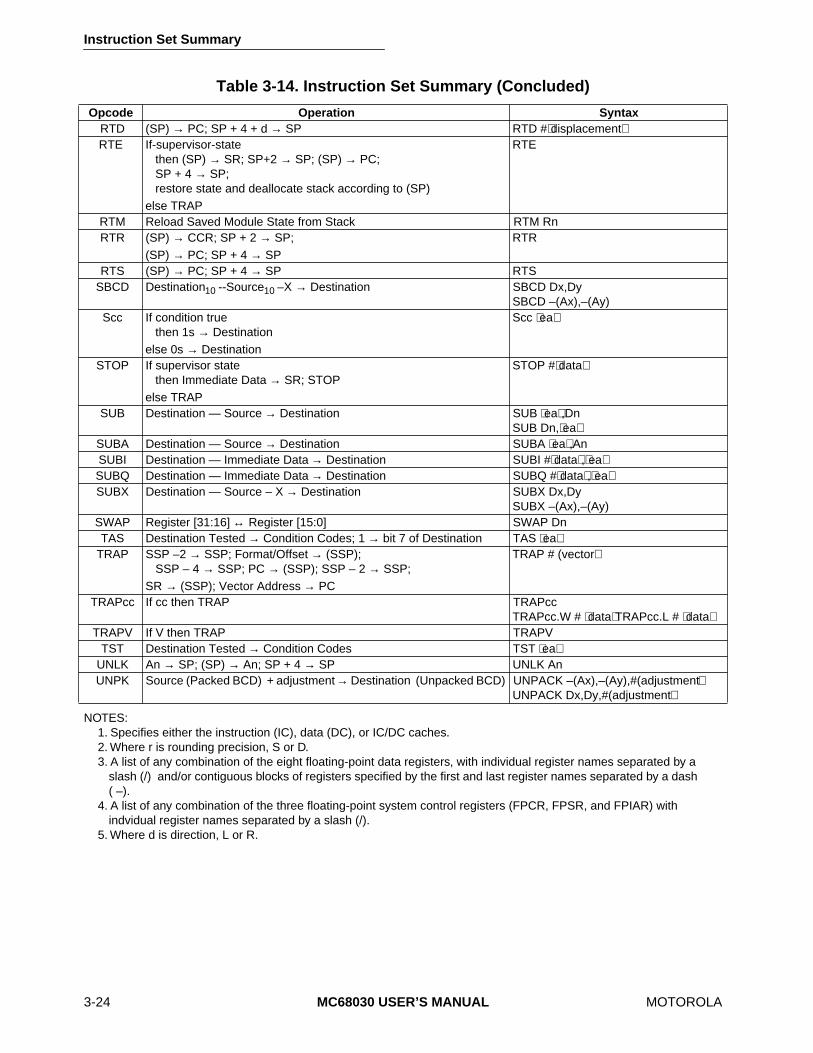
Instruction Set Summary
3-24 MC68030 USER’S MANUAL MOTOROLA
NOTES: 1. Specifies either the instruction (IC), data (DC), or IC/DC caches. 2. Where r is rounding precision, S or D. 3. A list of any combination of the eight floating-point data registers, with individual register names separated by a
slash (/) and/or contiguous blocks of registers specified by the first and last register names separated by a dash ( –).
4. A list of any combination of the three floating-point system control registers (FPCR, FPSR, and FPIAR) with indvidual register names separated by a slash (/).
5. Where d is direction, L or R.
Table 3-14. Instruction Set Summary (Concluded)
Opcode Operation Syntax RTD (SP) → PC; SP + 4 + d → SP RTD #⟨displacement⟩RTE If-supervisor-state
then (SP) → SR; SP+2 → SP; (SP) → PC; SP + 4 → SP; restore state and deallocate stack according to (SP)
else TRAP
RTE
RTM Reload Saved Module State from Stack RTM Rn RTR (SP) → CCR; SP + 2 → SP;
(SP) → PC; SP + 4 → SPRTR
RTS (SP) → PC; SP + 4 → SP RTS SBCD Destination10 --Source10 –X → Destination SBCD Dx,Dy
SBCD –(Ax),–(Ay) Scc If condition true
then 1s → Destinationelse 0s → Destination
Scc ⟨ea⟩
STOP If supervisor state then Immediate Data → SR; STOP
else TRAP
STOP #⟨data⟩
SUB Destination — Source → Destination SUB ⟨ea⟩,DnSUB Dn,⟨ea⟩
SUBA Destination — Source → Destination SUBA ⟨ea⟩,An SUBI Destination — Immediate Data → Destination SUBI #⟨data⟩,⟨ea⟩ SUBQ Destination — Immediate Data → Destination SUBQ #⟨data⟩,⟨ea⟩ SUBX Destination — Source – X → Destination SUBX Dx,Dy
SUBX –(Ax),–(Ay) SWAP Register [31:16] ↔ Register [15:0] SWAP Dn TAS Destination Tested → Condition Codes; 1 → bit 7 of Destination TAS ⟨ea⟩
TRAP SSP –2 → SSP; Format/Offset → (SSP);SSP – 4 → SSP; PC → (SSP); SSP – 2 → SSP;
SR → (SSP); Vector Address → PC
TRAP # (vector⟩
TRAPcc If cc then TRAP TRAPcc TRAPcc.W # ⟨data⟩TRAPcc.L # ⟨data⟩
TRAPV If V then TRAP TRAPV TST Destination Tested → Condition Codes TST ⟨ea⟩
UNLK An → SP; (SP) → An; SP + 4 → SP UNLK An UNPK Source (Packed BCD) + adjustment → Destination (Unpacked BCD) UNPACK –(Ax),–(Ay),#(adjustment⟩
UNPACK Dx,Dy,#(adjustment⟩

Instruction Set Summary
MOTOROLA MC68030 USER’S MANUAL 3-25
3.5 INSTRUCTION EXAMPLESThe following paragraphs provide examples of how to use selected instructions.
3.5.1 Using the CAS and CAS2 InstructionsThe CAS instruction compares the value in a memory location with the value in a dataregister, and copies a second data register into the memory location if the compared valuesare equal. This provides a means of updating system counters, history information, andglobally shared pointers. The instruction uses an indivisible read-modify-write cycle; afterCAS reads the memory location, no other instruction can change that location before CAShas written the new value. This provides security in single-processor systems, inmultitasking environments, and in multiprocessor environments. In a single-processorsystem, the operation is protected from instructions of an interrupt routine. In a multitaskingenvironment, no other task can interfere with writing the new value of a system variable. Ina multiprocessor environment, the other processors must wait until the CAS instructioncompletes before accessing a global pointer.
The following code fragment shows a routine to maintain a count, in location SYS_CNTR,of the executions of an operation that may be performed by any process or processor in asystem. The routine obtains the current value of the count in register D0 and stores the newcount value in register D1. The CAS instruction copies the new count into SYS_CNTR if itis valid. However, if another user has incremented the counter between the time the countwas stored and the read-modify-write cycle of the CAS instruction, the write portion of thecycle copies the new count in SYS_CNTR into D0, and the routine branches to repeat thetest. The following code sequence guarantees that SYS_CNTR is correctly incremented.
MOVE.W SYS_CNTR,D0 get the old value of the counterINC_LOOP MOVE.W D0,D1 make a copy of it
ADDQ.W #1,D1 and increment itCAS.W D0,D1,SYS_CNTR if countr value is still the same, update itBNE INC_LOOP if not, try again

Instruction Set Summary
3-26 MC68030 USER’S MANUAL MOTOROLA
The CAS and CAS2 instructions together allow safe operations in the manipulation ofsystem linked lists. Controlling a single location, HEAD in the example, manages a last-in-first-out linked list (see Figure 3–2). If the list is empty, HEAD contains the NULL pointer (0);otherwise, HEAD contains the address of the element most recently added to the list. Thecode fragment shown in Figure 3–2 illustrates the code for inserting an element. The MOVEinstructions load the address in location HEAD into D0 and into the NEXT pointer in theelement being inserted, and the address of the new element into D1. The CAS instructionstores the address of the inserted element into location HEAD if the address in HEADremains unaltered. If HEAD contains a new address, the instruction loads the new addressinto D0 and branches to the second MOVE instruction to try again.
The CAS2 instruction is similar to the CAS instruction except that it performs twocomparisons and updates two variables when the results of the comparisons are equal. Ifthe results of both comparisons are equal, CAS2 copies new values into the destinationaddresses. If the result of either comparison is not equal, the instruction copies the valuesin the destination addresses into the compare operands.
Figure 3-2. Linked List Insertion
SINSERTMOVE.L HEAD.D0MOVE.L D0, (NEXT, A1)MOVE.L A1, D1CAS.L D0, D1, HEADBNE SILOOP
ALLOCATE NEW ENTRY, ADDRESS IN A1MOVE HEAD POINTER VALUE TO D0ESTABLISH FORWARD LINK IN NEW ENTRYMOVE NEW ENTRY POINTER VALUE TO D1IF WE STILL POINT TO TOP OF STACK, UPDATE THE HEAD POINTERIF NOT, TRY AGAIN
SILOOP
ENTRY
+ NEXT
ENTRY
+ NEXT
ENTRY
+ NEXT
ENTRY
+ NEXT
NEWHEAD
NEW HEAD
AFTER INSERTING AN ELEMENT:
BEFORE INSERTING AN ELEMENT:
ENTRY
+ NEXT
ENTRY
+ NEXT
?
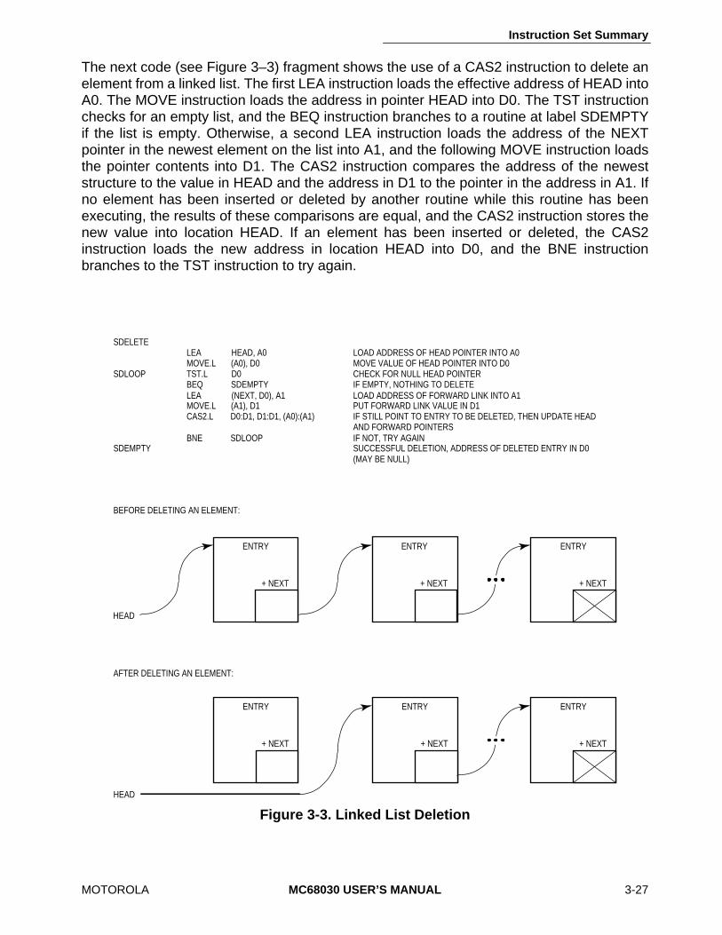
Instruction Set Summary
MOTOROLA MC68030 USER’S MANUAL 3-27
The next code (see Figure 3–3) fragment shows the use of a CAS2 instruction to delete anelement from a linked list. The first LEA instruction loads the effective address of HEAD intoA0. The MOVE instruction loads the address in pointer HEAD into D0. The TST instructionchecks for an empty list, and the BEQ instruction branches to a routine at label SDEMPTYif the list is empty. Otherwise, a second LEA instruction loads the address of the NEXTpointer in the newest element on the list into A1, and the following MOVE instruction loadsthe pointer contents into D1. The CAS2 instruction compares the address of the neweststructure to the value in HEAD and the address in D1 to the pointer in the address in A1. Ifno element has been inserted or deleted by another routine while this routine has beenexecuting, the results of these comparisons are equal, and the CAS2 instruction stores thenew value into location HEAD. If an element has been inserted or deleted, the CAS2instruction loads the new address in location HEAD into D0, and the BNE instructionbranches to the TST instruction to try again.
Figure 3-3. Linked List Deletion
HEAD
AFTER DELETING AN ELEMENT:
BEFORE DELETING AN ELEMENT:
SDELETE
SDLOOP
SDEMPTY
LEA HEAD, A0MOVE.L (A0), D0TST.L D0BEQ SDEMPTYLEA (NEXT, D0), A1MOVE.L (A1), D1CAS2.L D0:D1, D1:D1, (A0):(A1)
BNE SDLOOP
LOAD ADDRESS OF HEAD POINTER INTO A0MOVE VALUE OF HEAD POINTER INTO D0CHECK FOR NULL HEAD POINTERIF EMPTY, NOTHING TO DELETELOAD ADDRESS OF FORWARD LINK INTO A1PUT FORWARD LINK VALUE IN D1IF STILL POINT TO ENTRY TO BE DELETED, THEN UPDATE HEADAND FORWARD POINTERSIF NOT, TRY AGAINSUCCESSFUL DELETION, ADDRESS OF DELETED ENTRY IN D0(MAY BE NULL)
ENTRY
+ NEXT
ENTRY
+ NEXT
ENTRY
+ NEXT
ENTRY
+ NEXT
HEAD
ENTRY
+ NEXT
ENTRY
+ NEXT
Instruction Set Summary
3-28 MC68030 USER’S MANUAL MOTOROLA
The CAS2 instruction can also be used to correctly maintain a first-in-first-out doubly linkedlist. A doubly linked list needs two controlled locations, LIST_PUT and LIST_GET, whichcontain pointers to the last element inserted in the list and the next to be removed,respectively. If the list is empty, both pointers are NULL (0).
The code fragment shown in Figure 3–4 illustrates the insertion of an element in a doublylinked list. The first two instructions load the effective addresses of LIST_PUT andLIST_GET into registers A0 and A1, respectively. The next instruction moves the addressof the new element into register D2. Another MOVE instruction moves the address inLIST_PUT into register D0. At label DILOOP, a TST instruction tests the value in D0, andthe BEQ instruction branches to the MOVE instruction when D0 is equal to zero. Assumingthe list is empty, this MOVE instruction is executed next; it moves the zero in D0 into theNEXT and LAST pointers of the new element. Then the CAS2 instruction moves the addressof the new element into both LIST_PUT and LIST_GET, assuming that both of thesepointers still contain zero. If not, the BNE instruction branches to the TST instruction at labelDILOOP to try again. This time, the BEQ instruction does not branch, and the followingMOVE instruction moves the address in D0 to the NEXT pointer of the new element. TheCLR instruction clears register D1 to zero, and the MOVE instruction moves the zero intothe LAST pointer of the new element. The LEA instruction loads the address of the LASTpointer of the most recently inserted element into register A1. Assuming the LIST_PUTpointer and the pointer in A1 have not been changed, the CAS2 instruction stores theaddress of the new element into these pointers.
The code fragment to delete an element from a doubly linked list is similar (see Figure 3–5).The first two instructions load the effective addresses of pointers LIST_PUT and LIST_GETinto registers A0 and A1, respectively. The MOVE instruction at label DDLOOP moves theLIST_GET pointer into register D1. The BEQ instruction that follows branches out of theroutine when the pointer is zero. The MOVE instruction moves the LAST pointer of theelement to be deleted into register D2. Assuming this is not the last element in the list, theZ condition code is not set, and the branch to label DDEMPTY does not occur. The LEAinstruction loads the address of the NEXT pointer of the element at the address in D2 intoregister A2. The next instruction, a CLR instruction, clears register D0 to zero. The CAS2instruction compares the address in D1 to the LIST-GET pointer and to the address inregister A2. If the pointers have not been updated, the CAS2 instruction loads the addressin D2 into the LIST_GET pointer and zero into the address in register A2.
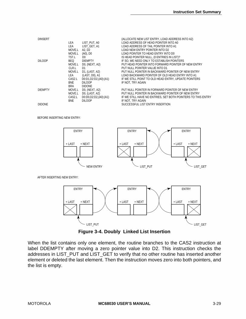
Instruction Set Summary
MOTOROLA MC68030 USER’S MANUAL 3-29
When the list contains only one element, the routine branches to the CAS2 instruction atlabel DDEMPTY after moving a zero pointer value into D2. This instruction checks theaddresses in LIST_PUT and LIST_GET to verify that no other routine has inserted anotherelement or deleted the last element. Then the instruction moves zero into both pointers, andthe list is empty.
Figure 3-4. Doubly Linked List Insertion
BEFORE INSERTING NEW ENTRY:
DINSERT
DILOOP
DIEMPTY
DIDONE
LEA LIST_PUT, A0LEA LIST_GET, A1MOVE.L A2, D2MOVE.L (A0), D0TST.L D0BEQ DIEMPTYMOVE.L D0, (NEXT, A2)CLR.L D1MOVE.L D1, (LAST, A2)LEA (LAST, D0), A1CAS2.L D0:D1,D2:D2,(A0):(A1)BNE DILOOPBRA DIDONEMOVE.L D0, (NEXT, A2)MOVE.L D0, (LAST, A2)CAS2.L D0:D0,D2:D2,(A0):(A1)BNE DILOOP
(ALLOCATE NEW LIST ENTRY, LOAD ADDRESS INTO A2)LOAD ADDRESS OF HEAD POINTER INTO A0LOAD ADDRESS OF TAIL POINTER INTO A1LOAD NEW ENTRY POINTER INTO D2LOAD POINTER TO HEAD ENTRY INTO D0IS HEAD POINTER NULL, (0 ENTRIES IN LIST)?IF SO, WE NEED ONLY TO ESTABLISH POINTERSPUT HEAD POINTER INTO FORWARD POINTER OF NEW ENTRYPUT NULL POINTER VALUE INTO D1PUT NULL POINTER IN BACKWARD POINTER OF NEW ENTRYLOAD BACKWARD POINTER OF OLD HEAD ENTRY INTO A1IF WE STILL POINT TO OLD HEAD ENTRY, UPDATE POINTERSIF NOT, TRY AGAIN
PUT NULL POINTER IN FORWARD POINTER OF NEW ENTRYPUT NULL POINTER IN BACKWARD POINTER OF NEW ENTRYIF WE STILL HAVE NO ENTRIES, SET BOTH POINTERS TO THIS ENTRYIF NOT, TRY AGAINSUCCESSFUL LIST ENTRY INSERTION
ENTRY ENTRY ENTRY
+ NEXT + NEXT + NEXT
AFTER INSERTING NEW ENTRY:
+ LAST+ LAST+ LAST
NEW ENTRY LIST_PUT LIST_GET
LIST_PUT
ENTRY ENTRY
+ NEXT + NEXT+ LAST+ LAST
LIST_GET
ENTRY
+ NEXT+ LAST
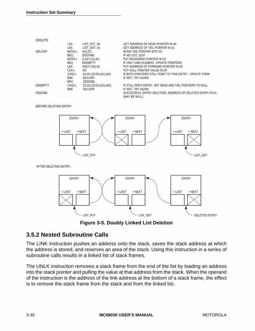
Instruction Set Summary
3-30 MC68030 USER’S MANUAL MOTOROLA
3.5.2 Nested Subroutine CallsThe LINK instruction pushes an address onto the stack, saves the stack address at whichthe address is stored, and reserves an area of the stack. Using this instruction in a series ofsubroutine calls results in a linked list of stack frames.
The UNLK instruction removes a stack frame from the end of the list by loading an addressinto the stack pointer and pulling the value at that address from the stack. When the operandof the instruction is the address of the link address at the bottom of a stack frame, the effectis to remove the stack frame from the stack and from the linked list.
Figure 3-5. Doubly Linked List Deletion
AFTER DELETING ENTRY:
BEFORE DELETING ENTRY:
DDELETE
DDLOOP
DDEMPTY
DDDONE
LEA LIST_PUT, A0LEA LIST_GET, A1MOVE.L (A1),D1BEQ DDDONEMOVE.L (LAST,D1),D2BEQ DDEMPTYLEA (NEXT,D2),A2CLR.L D0CAS2.L D1:D1,D2:D0,(A1):(A2)BNE DDLOOPBRA DDDONECAS2.L D1:D1,D2:D2,(A1):(A0)BNE DDLOOP
GET ADDRESS OF HEAD POINTER IN A0GET ADDRESS OF TAIL POINTER IN A1MOVE TAIL POINTER INTO D1IF NO LIST, QUITPUT BACKWARD POINTER IN D2IF ONLY ONE ELEMENT, UPDATE POINTERSPUT ADDRESS OF FORWARD POINTER IN A2PUT NULL POINTER VALUE IN D0IF BOTH POINTERS STILL POINT TO THIS ENTRY , UPDATE THEMIF NOT, TRY AGAIN
IF STILL FIRST ENTRY, SET HEAD AND TAIL POINTERS TO NULLIF NOT, TRY AGAINSUCCESSFUL ENTRY DELETION, ADDRESS OF DELETED ENTRY IN D1(MAY BE NULL)
ENTRY ENTRY ENTRY
+ NEXT + NEXT + NEXT+ LAST+ LAST+ LAST
LIST_PUT LIST_GET
LIST_PUT
ENTRY ENTRY
+ NEXT + NEXT+ LAST+ LAST
DELETED ENTRYLIST_GET
ENTRY
+ NEXT+ LAST

Instruction Set Summary
MOTOROLA MC68030 USER’S MANUAL 3-31
3.5.3 Bit Field OperationsOne data type provided by the MC68030 is the bit field, consisting of as many as 32consecutive bits. A bit field is defined by an offset from an effective address and a widthvalue. The offset is a value in the range of 231 through 231 1 from the most significant bit(bit 7) at the effective address. The width is a positive number, 1–32. The most significantbit of a bit field is bit 0; the bits number in a direction opposite to the bits of an integer.
The instruction set includes eight instructions that have bit field operands. The insert bit field(BFINS) instruction inserts a bit field stored in a register into a bit field. The extract bit fieldsigned (BFEXTS) instruction loads a bit field into the least significant bits of a register andextends the sign to the left, filling the register. The extract bit field unsigned (BFEXTU) alsoloads a bit field, but zero fills the unused portion of the destination register.
The set bit field (BFSET) instruction sets all the bits of a field to ones. The clear bit field(BFCLR) instruction clears a field. The change bit field (BFCHG) instruction complementsall the bits in a bit field. These three instructions all test the previous value of the bit field,setting the condition codes accordingly. The test bit field (BFTST) instruction tests the valuein the field, setting the condition codes appropriately without altering the bit field. The findfirst one in bit field (BFFFO) instruction scans a bit field from bit 0 to the right until it finds abit set to one and loads the bit offset of the first set bit into the specified data register. If nobits in the field are set, the field offset and the field width is loaded into the register.
An important application of bit field instructions is the manipulation of the exponent field in afloating-point number. In the IEEE standard format, the most significant bit is the sign bit ofthe mantissa. The exponent value begins at the next most significant bit position; theexponent field does not begin on a byte boundary. The extract bit field (BFEXTU) instructionand the BFTST instruction are the most useful for this application, but other bit fieldinstructions can also be used.
Programming of input and output operations to peripherals requires testing, setting, andinserting of bit fields in the control registers of the peripherals, which is another applicationfor bit field instructions. However, control register locations are not memory locations;therefore, it is not always possible to insert or extract bit fields of a register without affectingother fields within the register.
Instruction Set Summary
MOTOROLA MC68030 USER’S MANUAL 3-32
Another widely used application for bit field instructions is bit-mapped graphics. Becausebyte boundaries are ignored in these areas of memory, the field definitions used with bit fieldinstructions are very helpful.
3.5.4 Pipeline Synchronization with the Nop InstructionAlthough the no operation (NOP) instruction performs no visible operation, it serves animportant purpose. It forces synchronization of the integer unit pipeline by waiting for allpending bus cycles to complete. All previous integer instructions and floating-point externaloperand accesses complete execution before the NOP begins. The NOP instruction doesnot synchronize the FPU pipeline; floating-point instructions with floating-point registeroperand destinations can be executing when the NOP begins.
MOTOROLA
MC68030 USER’S MANUAL
4-1
SECTION 4PROCESSING STATES
This section describes the processing states of the MC68030. It describes the functions ofthe bits in the supervisor portion of the status register and the actions taken by the processorin response to exception conditions.
Unless the processor has halted, it is always in either the normal or the exception processingstate. Whenever the processor is executing instructions or fetching instructions or operands,it is in the normal processing state. The processor is also in the normal processing statewhile it is storing instruction results or communicating with a coprocessor.
NOTE
Exception processing refers specifically to the transition fromnormal processing of a program to normal processing of systemroutines, interrupt routines, and other exception handlers. Ex-ception processing includes all stacking operations, the fetch ofthe exception vector, and filling of the instruction pipe caused byan exception. It has completed when execution of the first in-struction of the exception handler routine begins.
The processor enters the exception processing state when an interrupt is acknowledged,when an instruction is traced or results in a trap, or when some other exceptional conditionarises. Execution of certain instructions or unusual conditions occurring during the executionof any instructions can cause exceptions. External conditions, such as interrupts, bus errors,and some coprocessor responses, also cause exceptions. Exception processing providesan efficient transfer of control to handlers and routines that process the exceptions.
A catastrophic system failure occurs whenever the processor receives a bus error orgenerates an address error while in the exception processing state. This type of failure haltsthe processor. For example, if during the exception processing of one bus error another buserror occurs, the MC68030 has not completed the transition to normal processing and hasnot completed saving the internal state of the machine, so the processor assumes that thesystem is not operational and halts. Only an external reset can restart a halted processor.(When the processor executes a STOP instruction, it is in a special type of normalprocessing state, one without bus cycles. It is stopped, not halted.)
Processing States
4-2
MC68030 USER’S MANUAL
MOTOROLA
4.1 PRIVILEGE LEVELS
The processor operates at one of two levels of privilege: the user level or the supervisorlevel. The supervisor level has higher privileges than the user level. Not all processor orcoprocessor instructions are permitted to execute in the lower privileged user level, but allare available at the supervisor level. This allows a separation of supervisor and user so thesupervisor can protect system resources from uncontrolled access. The processor uses theprivilege level indicated by the S bit in the status register to select either the user orsupervisor privilege level and either the user stack pointer or a supervisor stack pointer forstack operations. The processor identifies a bus access (supervisor or user mode) via thefunction codes so that differentiation between supervisor and user can be maintained. Thememory management unit uses the indication of privilege level to control and translatememory accesses to protect supervisor code, data, and resources from access by userprograms.
In many systems, the majority of programs execute at the user level. User programs canaccess only their own code and data areas and can be restricted from accessing otherinformation. The operating system typically executes at the supervisor privilege level. It hasaccess to all resources, performs the overhead tasks for the user level programs, andcoordinates their activities.
4.1.1 Supervisor Privilege Level
The supervisor level is the higher privilege level. The privilege level is determined by the Sbit of the status register; if the S bit is set, the supervisor privilege level applies, and allinstructions are executable. The bus cycles for instructions executed at the supervisor levelare normally classified as supervisor references, and the values of the function codes onFC0–FC2 refer to supervisor address spaces.
In a multitasking operating system, it is more efficient to have a supervisor stack spaceassociated with each user task and a separate stack space for interrupt associated tasks.The MC68030 provides two supervisor stacks, master and interrupt; the M bit of the statusregister selects which of the two is active. When the M bit is set to one, supervisor stackpointer references (either implicit or by specifying address register A7) access the masterstack pointer (MSP). The operating system sets the MSP for each task to point to a task-related area of supervisor data space. This separates task-related supervisor activity fromasynchronous, I/O-related supervisor tasks that may be only coincidental to the currentlyexecuting task. The master stack (MSP) can separately maintain task control information foreach currently executing user task, and the software updates the MSP when a task switchis performed, providing an efficient means for transferring task-related stack items. Theother supervisor stack (ISP) can be used for interrupt control information and workspacearea as interrupt handling routines require.
Processing States
MOTOROLA
MC68030 USER’S MANUAL
4-3
When the M bit is clear, the MC68030 is in the interrupt mode of the supervisor privilegelevel, and operation is the same as in the MC68000, MC68008, and MC68010 supervisormode. (The processor is in this mode after a reset operation.) All supervisor stack pointerreferences access the interrupt stack pointer (ISP) in this mode.
The value of the M bit in the status register does not affect execution of privilegedinstructions; both master and interrupt modes are at the supervisor privilege level.Instructions that affect the M bit are MOVE to SR, ANDI to SR, EORI to SR, ORI to SR, andRTE. Also, the processor automatically saves the M-bit value and clears it in the SR as partof the exception processing for interrupts.
All exception processing is performed at the supervisor privilege level. All bus cyclesgenerated during exception processing are supervisor references, and all stack accessesuse the active supervisor stack pointer.
4.1.2 User Privilege Level
The user level is the lower privilege level. The privilege level is determined by the S bit ofthe status register; if the S bit is clear, the processor executes instructions at the userprivilege level.
Most instructions execute at either privilege level, but some instructions that have importantsystem effects are privileged and can only be executed at the supervisor level. For instance,user programs are not allowed to execute the STOP instruction or the RESET instruction.To prevent a user program from entering the supervisor privilege level, except in a controlledmanner, instructions that can alter the S bit in the status register are privileged. The TRAP#n instruction provides controlled access to operating system services for user programs.
Processing States
4-4
MC68030 USER’S MANUAL
MOTOROLA
The bus cycles for an instruction executed at the user privilege level are classified as userreferences, and the values of the function codes on FC0-FC2 specify user address spaces.The memory management unit of the processor, when it is enabled, uses the value of thefunction codes to distinguish between user and supervisor activity and to control access toprotected portions of the address space. While the processor is at the user level, referencesto the system stack pointer implicitly, or to address register seven (A7) explicitly, refer to theuser stack pointer (USP).
4.1.3 Changing Privilege Level
To change from the user to the supervisor privilege level, one of the conditions that causesthe processor to perform exception processing must occur. This causes a change from theuser level to the supervisor level and can cause a change from the master mode to theinterrupt mode. Exception processing saves the current values of the S and M bits of thestatus register (along with the rest of the status register) on the active supervisor stack, andthen sets the S bit, forcing the processor into the supervisor privilege level. When theexception being processed is an interrupt and the M bit is set, the M bit is cleared, puttingthe processor into the interrupt mode. Execution of instructions continues at the supervisorlevel to process the exception condition.
To return to the user privilege level, a system routine must execute one of the followinginstructions: MOVE to SR, ANDI to SR, EORI to SR, ORI to SR, or RTE. The MOVE, ANDI,EORI, and ORI to SR and RTE instructions execute at the supervisor privilege level and canmodify the S bit of the status register. After these instructions execute, the instructionpipeline is flushed and is refilled from the appropriate address space. This is indicatedexternally by the assertion of the REFILL signal.
The RTE instruction returns to the program that was executing when the exception occurred.It restores the exception stack frame saved on the supervisor stack. If the frame on top ofthe stack was generated by an interrupt, trap, or instruction exception, the RTE instructionrestores the status register and program counter to the values saved on the supervisorstack. The processor then continues execution at the restored program counter address andat the privilege level determined by the S bit of the restored status register. If the frame ontop of the stack was generated by a bus fault (bus error or address error exception), the RTEinstruction restores the entire saved processor state from the stack.

Processing States
MOTOROLA
MC68030 USER’S MANUAL
4-5
4.2 ADDRESS SPACE TYPES
The processor specifies a target address space for every bus cycle with the function codesignals according to the type of access required. In addition to distinguishing betweensupervisor/user and program/data, the processor can identify special processor cycles,such as the interrupt acknowledge cycle, and the memory management unit can controlaccesses and translate addresses appropriately. Table 4-1 lists the types of accessesdefined for the MC68030 and the corresponding values of function codes FC0–FC2.
*Address space 3 is reserved for user definition; whereas, 0 and 4 are reserved for future use by Motorola.
The memory locations of user program and data accesses are not predefined. Neither arethe locations of supervisor data space. During reset, the first two long words beginning atmemory location zero in the supervisor program space are used for processor initialization.No other memory locations are explicitly defined by the MC68030.
A function code of $7 ([FC2:FC0] = 111) selects the CPU address space. This is a specialaddress space that does not contain instructions or operands but is reserved for specialprocessor functions. The processor uses accesses in this space to communicate withexternal devices for special purposes. For example, all M68000 processors use the CPUspace for interrupt acknowledge cycles. The MC68020 and MC68030 also generate CPUspace accesses for breakpoint acknowledge and coprocessor operations.
Supervisor programs can use the MOVES instruction to access all address spaces,including the user spaces and the CPU address space. Although the MOVES instruction canbe used to generate CPU space cycles, this may interfere with proper system operation.Thus, the use of MOVES to access the CPU space should be done with caution.
Table 4-1. Address Space Encodings
FC2 FC1 FC0 Address Space
0 0 0 (Undefined, Reserved)*0 0 1 User Data Space0 1 0 User Program Space0 1 1 (Undefined, Reserved)*1 0 0 (Undefined, Reserved)*1 0 1 Supervisor Data Space1 1 0 Supervisor Program Space1 1 1 CPU Space

Processing States
4-6
MC68030 USER’S MANUAL
MOTOROLA
4.3 EXCEPTION PROCESSING
An exception is defined as a special condition that pre-empts normal processing. Bothinternal and external conditions cause exceptions. External conditions that causeexceptions are interrupts from external devices, bus errors, coprocessor detected errors,and reset. Instructions, address errors, tracing, and breakpoints are internal conditions thatcause exceptions. The TRAP, TRAPcc, TRAPV, cpTRAPcc, CHK, CHK2, RTE, and DIVinstructions can all generate exceptions as part of their normal execution. In addition, illegalinstructions, privilege violations, and coprocessor protocol violations cause exceptions.
Exception processing, which is the transition from the normal processing of a program to theprocessing required for the exception condition, involves the exception vector table and anexception stack frame. The following paragraphs describe the vector table and ageneralized exception stack frame. Exception processing is discussed in detail in
Section8 Exception Processing
.
Coprocessor detected exceptions are discussed in detail in
Section 10 Coprocessor Interface Description
.
4.3.1 Exception Vectors
The vector base register (VBR) contains the base address of the 1024-byte exception vectortable, which consists of 256 exception vectors. Exception vectors contain the memoryaddresses of routines that begin execution at the completion of exception processing. Theseroutines perform a series of operations appropriate for the corresponding exceptions.Because the exception vectors contain memory addresses, each consists of one long word,except for the reset vector. The reset vector consists of two long words: the address usedto initialize the interrupt stack pointer and the address used to initialize the program counter.
The address of an exception vector is derived from an 8-bit vector number and the VBR. Thevector numbers for some exceptions are obtained from an external device; others aresupplied automatically by the processor. The processor multiplies the vector number by fourto calculate the vector offset, which it adds to the VBR. The sum is the memory address ofthe vector. All exception vectors are located in supervisor data space, except the resetvector, which is located in supervisor program space. Only the initial reset vector is fixed inthe processor's memory map; once initialization is complete, there are no fixedassignments. Since the VBR provides the base address of the vector table, the vector tablecan be located anywhere in memory; it can even be dynamically relocated for each task thatis executed by an operating system. Details of exception processing are provided in
Section8 Exception Processing
, and Table 8-1 lists the exception vector assignments.
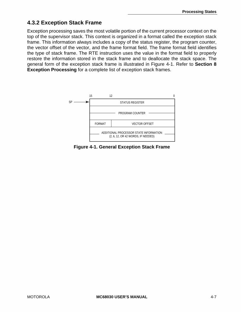
Processing States
MOTOROLA
MC68030 USER’S MANUAL
4-7
4.3.2 Exception Stack Frame
Exception processing saves the most volatile portion of the current processor context on thetop of the supervisor stack. This context is organized in a format called the exception stackframe. This information always includes a copy of the status register, the program counter,the vector offset of the vector, and the frame format field. The frame format field identifiesthe type of stack frame. The RTE instruction uses the value in the format field to properlyrestore the information stored in the stack frame and to deallocate the stack space. Thegeneral form of the exception stack frame is illustrated in Figure 4-1. Refer to
Section 8Exception Processing
for a complete list of exception stack frames.
Figure 4-1. General Exception Stack Frame
STATUS REGISTER
FORMAT VECTOR OFFSET
15 12 0
SP
PROGRAM COUNTER
ADDITIONAL PROCESSOR STATE INFORMATION (2, 6, 12, OR 42 WORDS, IF NEEDED)
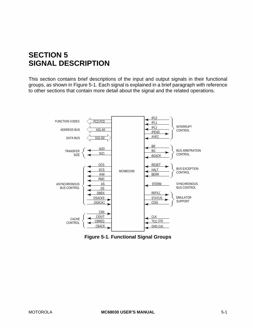
MOTOROLA
MC68030 USER’S MANUAL
5-1
SECTION 5SIGNAL DESCRIPTION
This section contains brief descriptions of the input and output signals in their functionalgroups, as shown in Figure 5-1. Each signal is explained in a brief paragraph with referenceto other sections that contain more detail about the signal and the related operations.
Figure 5-1. Functional Signal Groups
DSACK0
FUNCTION CODES
ADDRESS BUS
TRANSFERSIZE
ASYNCHRONOUSBUS CONTROL
CACHECONTROL
EMULATORSUPPORT
SYNCHRONOUSBUS CONTROL
BUS EXCEPTIONCONTROL
BUS ARBITRATIONCONTROL
INTERRUPTCONTROL
FC2-FC0
A31-A0
D31-D0
SIZ0SIZ1
OCS
ECSR/W
RMC
ASDS
DBEN
DSACK1
CIINCIOUT
CBREQ
CBACK GND (14)
CLK
CDISSTATUS
REFILL
STERM
BERRHALT
RESET
IPL0IPL1
IPL2IPENDAVEC
BRBG
BGACK
V (10)CC
DATA BUS
MC68EC030
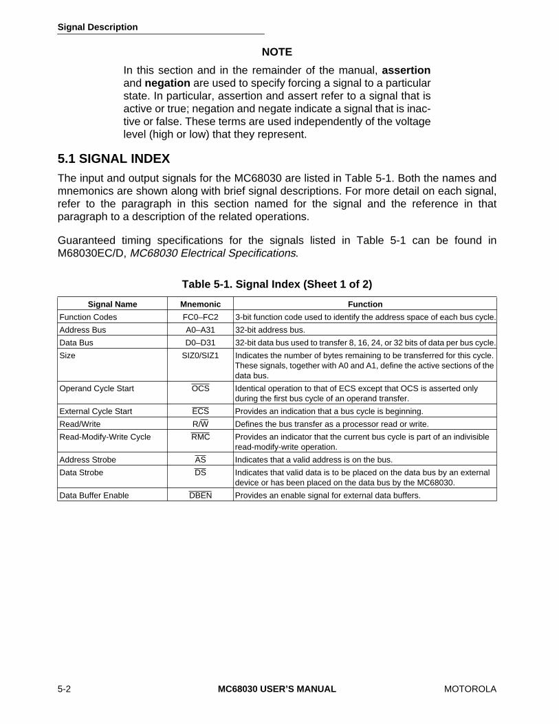
Signal Description
5-2
MC68030 USER’S MANUAL
MOTOROLA
NOTE
In this section and in the remainder of the manual,
assertion
and
negation
are used to specify forcing a signal to a particularstate. In particular, assertion and assert refer to a signal that isactive or true; negation and negate indicate a signal that is inac-tive or false. These terms are used independently of the voltagelevel (high or low) that they represent.
5.1 SIGNAL INDEX
The input and output signals for the MC68030 are listed in Table 5-1. Both the names andmnemonics are shown along with brief signal descriptions. For more detail on each signal,refer to the paragraph in this section named for the signal and the reference in thatparagraph to a description of the related operations.
Guaranteed timing specifications for the signals listed in Table 5-1 can be found inM68030EC/D,
MC68030 Electrical Specifications
.
Table 5-1. Signal Index (Sheet 1 of 2)
Signal Name Mnemonic Function
Function Codes FC0–FC2 3-bit function code used to identify the address space of each bus cycle.
Address Bus A0–A31 32-bit address bus.
Data Bus D0–D31 32-bit data bus used to transfer 8, 16, 24, or 32 bits of data per bus cycle.
Size SIZ0/SIZ1 Indicates the number of bytes remaining to be transferred for this cycle. These signals, together with A0 and A1, define the active sections of the data bus.
Operand Cycle Start OCS Identical operation to that of ECS except that OCS is asserted only during the first bus cycle of an operand transfer.
External Cycle Start ECS Provides an indication that a bus cycle is beginning.
Read/Write R/W Defines the bus transfer as a processor read or write.
Read-Modify-Write Cycle RMC Provides an indicator that the current bus cycle is part of an indivisible read-modify-write operation.
Address Strobe AS Indicates that a valid address is on the bus.
Data Strobe DS Indicates that valid data is to be placed on the data bus by an external device or has been placed on the data bus by the MC68030.
Data Buffer Enable DBEN Provides an enable signal for external data buffers.

Signal Description
MOTOROLA
MC68030 USER’S MANUAL
5-3
Table 5-1. Signal Index (Sheet 2 of 2)
Signal Name Mnemonic Function
Data Transfer and Size Acknowledge
DSACK0/DSACK1
Bus response signals that indicate the requested data transfer operation is completed. In addition, these two lines indicate the size of the external bus port on a cycle-by-cycle basis and are used for asynchronous transfers.
Synchronous Termination
STERM Bus response signal that indicates a port size of 32 bits and that data may be latched on the next falling clock edge.
Cache Inhibit In CIIN Prevents data from being loaded into the MC68030 instruction and data caches.
Cache Inhibit Out CIOUT Reflects the CI bit in ATC entries or TTx register; indicates that external caches should ignore these accesses
Cache Burst Request CBREQ Indicates a burst request for the instruction or data cache.
Cache Burst Acknowledge
CBACK Indicates that the accessed device can operate in burst mode.
Interrupt Priority Level IPL0–IPL2 Provides an encoded interrupt level to the processor.
Interrupt Pending IPEND Indicates that an interrupt is pending.
Autovector AVEC Requests an autovector during an interrupt acknowledge cycle.
Bus Request BR Indicates that an external device requires bus mastership.
Bus Grant BG Indicates that an external device may assume bus mastership.
Bus Grant Acknowledge BGACK Indicates that an external device has assumed bus mastership.
Reset RESET System reset.
Halt HALT Indicates that the processor should suspend bus activity.
Bus Error BERR Indicates that an erroneous bus operation is being attempted.
Cache Disable CDIS Dynamically disables the on-chip cache to assist emulator support.
MMU Disable MMUDIS Dynamically disables the translation mechanism of the MMU.
Pipe Refill REFILL Indicates when the MC68030 is beginning to fill pipeline.
Microsequencer Status STATUS Indicates the state of the microsequencer
Clock CLK Clock input to the processor.
Power Supply V
CC
Power supply.
Ground GND Ground connection

Signal Description
5-4
MC68030 USER’S MANUAL
MOTOROLA
5.2 FUNCTION CODE SIGNALS (FC0
–
FC2)
These three-state outputs identify the address space of the current bus cycle. Table 4-1shows the relationship of the function code signals to the privilege levels and the addressspaces. Refer to
4.2 Address Space Types
for more information.
5.3 ADDRESS BUS (A0
–
A31)
These three-state outputs provide the address for the current bus cycle, except in the CPUaddress space. Refer to
4.2 Address Space Types
for more information on the CPUaddress space. A31 is the most significant address signal. Refer to
7.1.2 Address Bus
forinformation on the address bus and its relationship to bus operation.
5.4 DATA BUS (D0
–
D31)
These three-state bidirectional signals provide the general-purpose data path between theMC68030 and all other devices. The data bus can transfer 8, 16, 24, or 32 bits of data perbus cycle. D31 is the most significant bit of the data bus. Refer to
7.1.4 Data Bus
for moreinformation on the data bus and its relationship to bus operation.
5.5 TRANSFER SIZE SIGNALS (SIZ0, SIZ1)
These three-state outputs indicate the number of bytes remaining to be transferred for thecurrent bus cycle. With A0, A1, DSACK0, DSACK1, and STERM, SIZ0 and SIZ1 define thenumber of bits transferred on the data bus. Refer to
7.2.1 Dynamic Bus Sizing
for moreinformation on the size signals and their use in dynamic bus sizing.

Signal Description
MOTOROLA
MC68030 USER’S MANUAL
5-5
5.6 BUS CONTROL SIGNALS
The following signals control synchronous bus transfer operations for the MC68030.
5.6.1 Operand Cycle Start (OCS)
This output signal indicates the beginning of the first external bus cycle for an instructionprefetch or a data operand transfer. OCS is not asserted for subsequent cycles that areperformed due to dynamic bus sizing or operand misalignment.
7.1.1 Bus Control Signals
for information about the relationship of OCS to bus operation.
5.6.2 External Cycle Start (ECS)
This output signal indicates the beginning of a bus cycle of any type.
7.1.1 Bus ControlSignals
for information about the relationship of ECS to bus operation.
5.6.3 Read/Write (R/W)
This three-state output signal defines the type of bus cycle. A high level indicates a readcycle; a low level indicates a write cycle. Refer to
7.1.1 Bus Control Signals
for informationabout the relationship of R/W to bus operation.
5.6.4 Read-Modify-Write Cycle (RMC)
This three-state output signal identifies the current bus cycle as part of an indivisible read-modify-write operation; it remains asserted during all bus cycles of the read-modify-writeoperation. Refer to
7.1.1 Bus Control Signals
for information about the relationship of RMCto bus operation.
5.6.5 Address Strobe (AS)
This three-state output indicates that a valid address is on the address bus. The functioncode, size, and read/write signals are also valid when AS is asserted. Refer to
7.1.3Address Strobe
for information about the relationship of AS to bus operation.

Signal Description
5-6
MC68030 USER’S MANUAL
MOTOROLA
5.6.6 Data Strobe (DS)
During a read cycle, this three-state output indicates that an external device should placevalid data on the data bus. During a write cycle, the data strobe indicates that the MC68030has placed valid data on the bus. During two-clock synchronous write cycles, the MC68030does not assert DS. Refer to
7.1.5 Data Strobe
for more information about the relationshipof DS to bus operation.
5.6.7 Data Buffer Enable (DBEN)
This output is an enable signal for external data buffers. This signal may not be required inall systems. The timing of this signal may preclude its use in a system that supports two-clock synchronous bus cycles. Refer to
7.1.6 Data Buffer Enable
for more informationabout the relationship of DBEN to bus operation.
5.6.8 Data Transfer and Size Acknowledge (DSACK0, DSACK1)
These inputs indicate the completion of a requested data transfer operation. In addition, theyindicate the size of the external bus port at the completion of each cycle. These signals applyonly to asynchronous bus cycles. Refer to
7.1.7 Bus Cycle Termination Signals
for moreinformation on these signals and their relationship to dynamic bus sizing.
5.6.9 Synchronous Termination (STERM)
This input is a bus handshake signal indicating that the addressed port size is 32 bits andthat data is to be latched on the next falling clock edge for a read cycle. This signal appliesonly to synchronous operation. Refer to
7.1.7 Bus Cycle Termination Signals
for moreinformation about the relationship of STERM to bus operation.

Signal Description
MOTOROLA
MC68030 USER’S MANUAL
5-7
5.7 CACHE CONTROL SIGNALS
The following signals relate to the on-chip caches.
5.7.1 Cache Inhibit Input (CIIN)
This input signal prevents data from being loaded into the MC68030 instruction and datacaches. It is a synchronous input signal and is interpreted on a bus-cycle-by-bus-cyclebasis. CIIN is ignored during all write cycles. Refer to
6.1 On-Chip Cache Organizationand Operation
for information on the relationship of CIIN to the on-chip caches.
5.7.2 Cache Inhibit Output (CIOUT)
This three-state output signal reflects the state of the CI bit in the address translation cacheentry for the referenced logical address, indicating that an external cache should ignore thebus transfer. When the referenced logical address is within an area specified for transparenttranslation, the CI bit of the appropriate transparent translation register controls the state ofCIOUT. Refer to
Section 9 Memory Management Unit
for more information about theaddress translation cache and transparent translation. Also, refer to
Section 6 On-ChipCache Memories
for the effect of CIOUT on the internal caches.
5.7.3 Cache Burst Request (CBREQ)
This three-state output signal requests a burst mode operation to fill a line in the instructionor data cache. Refer to
6.1.3 Cache Filling
for filling information and
7.3.7 Burst OperationCycles
for bus cycle information pertaining to burst mode operations.
5.7.4 Cache Burst Acknowledge (CBACK)
This input signal indicates that the accessed device can operate in the burst mode and cansupply at least one more long word for the instruction or data cache. Refer to
7.3.7 BurstOperation Cycles
for information about burst mode operation.

Signal Description
5-8
MC68030 USER’S MANUAL
MOTOROLA
5.8 INTERRUPT CONTROL SIGNALS
The following signals are the interrupt control signals for the MC68030.
5.8.1 Interrupt Priority Level Signals
These input signals provide an indication of an interrupt condition and the encoding of theinterrupt level from a peripheral or external prioritizing circuitry. IPL2 is the most significantbit of the level number. For example, since the IPLn signals are active low, IPL0–IPL2 equalto $5 corresponds to an interrupt request at interrupt level 2. Refer to
8.1.9 InterruptExceptions
for information on MC68030 interrupts.
5.8.2 Interrupt Pending (IPEND)
This output signal indicates that an interrupt request has been recognized internally andexceeds the current interrupt priority mask in the status register (SR). This output is for useby external devices (coprocessors and other bus masters, for example) to predict processoroperation on the following instruction boundaries. Refer to
8.1.9 Interrupt Exceptions
forinterrupt information. Also, refer to
7.4.1 Interrupt Acknowledge Bus Cycles
for businformation related to interrupts.
5.8.3 Autovector (AVEC)
This input signal indicates that the MC68030 should generate an automatic vector during aninterrupt acknowledge cycle. Refer to
7.4.1.2 Autovector Interrupt Acknowledge Cycle
for more information about automatic vectors.
5.9 BUS ARBITRATION CONTROL SIGNALS
The following signals are the three bus arbitration control signals used to determine whichdevice in a system is the bus master.
5.9.1 Bus Request (BR)
This input signal indicates that an external device needs to become the bus master. This istypically a "wire-ORed” input (but does not need to be constructed from open-collectordevices). Refer to
7.7 Bus Arbitration
for more information.
Signal Description
MOTOROLA
MC68030 USER’S MANUAL
5-9
5.9.2 Bus Grant (BG)
This output indicates that the MC68030 will release ownership of the bus master when thecurrent processor bus cycle completes. Refer to
7.7.2 Bus Grant
for more information.
5.9.3 Bus Grant Acknowledge (BGACK)
This input indicates that an external device has become the bus master. Refer to
7.7.3 BusGrant Acknowledge
for more information.
5.10 BUS EXCEPTION CONTROL SIGNALS
The following signals are the bus exception control signals for the MC68030.
5.10.1 Reset (RESET)
This bidirectional open-drain signal is used to initiate a system reset. An external reset signalresets the MC68030 as well as all external devices. A reset signal from the processor(asserted as part of the RESET instruction) resets external devices only; the internal stateof the processor is not altered. Refer to
7.8 Reset Operation
for a description of reset busoperation and 8.1.1 Reset Exception for information about the reset exception.
5.10.2 Halt (HALT)The halt signal indicates that the processor should suspend bus activity or, when used withBERR, that the processor should retry the current cycle. Refer to 7.5 Bus ExceptionControl Cycles for a description of the effects of HALT on bus operations.
5.10.3 Bus Error (BERR)The bus error signal indicates that an invalid bus operation is being attempted or, when usedwith HALT, that the processor should retry the current cycle. Refer to 7.5 Bus ExceptionControl Cycles for a description of the effects of BERR on bus operations.
Signal Description
5-10 MC68030 USER’S MANUAL MOTOROLA
5.11 EMULATOR SUPPORT SIGNALSThe following signals support emulation by providing a means for an emulator to disable theon-chip caches and memory management unit and by supplying internal status informationto an emulator. Refer to Section 12 Applications Information for more detailedinformation on emulation support.
5.11.1 Cache Disable (CDIS)The cache disable signal dynamically disables the on-chip caches to assist emulatorsupport. Refer to 6.1 On-Chip Cache Organization and Operation for information aboutthe caches; refer to Section 12 Applications Information for a description of the use ofthis signal by an emulator. CDIS does not flush the data and instruction caches; entriesremain unaltered and become available again when CDIS is negated.
5.11.2 MMU Disable (MMUDIS)The MMU disable signal dynamically disables the translation of addresses by the MMU.Refer to 9.4 Address Translation Cache for a description of address translation; refer toSection 12 Applications Information for a description of the use of this signal by anemulator. The assertion of MMUDIS does not flush the address translation cache (ATC);ATC entries become available again when MMUDIS is negated.
5.11.3 Pipeline Refill (REFILL)The pipeline refill signal indicates that the MC68030 is beginning to refill the internalinstruction pipeline. Refer to Section 12 Applications Information for a description of theuse of this signal by an emulator.
5.11.4 Internal Microsequencer Status (STATUS)The microsequencer status signal indicates the state of the internal microsequencer. Thevarying number of clocks for which this signal is asserted indicates instruction boundaries,pending exceptions, and the halted condition. Refer to Section 12 ApplicationsInformation for a description of the use of this signal by an emulator.

Signal Description
5-11 MC68030 USER’S MANUAL MOTOROLA
5.12 CLOCK (CLK)The clock signal is the clock input to the MC68030. It is a TTL-compatible signal. Refer toSection 12 Applications Information for suggestions on clock generation.
5.13 POWER SUPPLY CONNECTIONSThe MC68030 requires connection to a VCC power supply, positive with respect to ground.The VCC connections are grouped to supply adequate current for the various sections of theprocessor. The ground connections are similarly grouped. Section 14 OrderingInformation and Mechanical Data describes the groupings of VCC and groundconnections, and Section 12 Applications Information describes a typical power supplyinterface.
5.14 SIGNAL SUMMARYTable 5-2 provides a summary of the electrical characteristics of the signals discussed inthis section.

Signal Description
5-12 MC68030 USER’S MANUAL MOTOROLA
Table 5-2. Signal Summary
Signal Function Signal Name Input/Output Active State Three-State
Function Codes FC0–FC2 Output High Yes
Address Bus A0–A31 Output High Yes
Data Bus D0–D31 Input/Output High Yes
Transfer Size SIZ0/SIZ1 Output High Yes
Operand Cycle Start OCS Output Low No
External Cycle Start ECS Output Low No
Read/Write R/W Output High/Low Yes
Read-Modify-Write Cycle RMC Output Low Yes
Address Strobe AS Output Low Yes
Data Strobe DS Output Low Yes
Data Buffer Enable DBEN Output Low Yes
Data Transfer and Size Acknowledge
DSACK0/DSACK1
Input Low —
Synchronous Termination STERM Input Low —
Cache Inhibit In CIIN Input Low —
Cache Inhibit Out CIOUT Output Low Yes
Cache Burst Request CBREQ Output Low Yes
Cache Burst Acknowledge CBACK Input Low —
Interrupt Priority Level IPL0–IPL2 Input Low —
Interrupt Pending IPEND Output Low No
Autovector AVEC Input Low —
Bus Request BR Input Low —
Bus Grant BG Output Low No
Bus Grant Acknowledge BGACK Input Low —
Reset RESET Input/Output Low No
Halt HALT Input Low —
Bus Error BERR Input Low —
Cache Disable CDIS Input Low —
MMU Disable MMUDIS Input Low —
Pipeline Refill REFILL Output Low No
Microsequencer Status STATUS Output Low No
Clock CLK Input — —
Power Supply VCC Input — —
Ground GND Input — —
MOTOROLA
MC68030 USER’S MANUAL
6-1
SECTION 6 ON-CHIP CACHE MEMORIES
The MC68030 microprocessor includes a 256-byte on-chip instruction cache and a 256-byteon-chip data cache that are accessed by logical (virtual) addresses. These caches improveperformance by reducing external bus activity and increasing instruction throughput.
Reduced external bus activity increases overall performance by increasing the availabilityof the bus for use by external devices (in systems with more than one bus master, such asa processor and a DMA device) without degrading the performance of the MC68030. Anincrease in instruction throughput results when instruction words and data required by aprogram are available in the on-chip caches and the time required to access them on theexternal bus is eliminated. Additionally, instruction throughput increases when instructionwords and data can be accessed simultaneously.
As shown in Figure 6-1, the instruction cache and the data cache are connected to separateon-chip address and data buses. The address buses are combined to provide the logicaladdress to the memory management unit (MMU). The MC68030 initiates an access to theappropriate cache for the requested instruction or data operand at the same time that itinitiates an access for the translation of the logical address in the address translation cacheof the MMU. When a hit occurs in the instruction or data cache and the MMU validates theaccess on a write, the information is transferred from the cache (on a read) or to the cacheand the bus controller (on a write). When a hit does not occur, the MMU translation of theaddress is used for an external bus cycle to obtain the instruction or operand. Regardlessof whether or not the required operand is located in one of the on-chip caches, the addresstranslation cache of the MMU performs logical-to-physical address translation in parallelwith the cache lookup in case an external cycle is required.
On-Chip Cache Memories
6-2
MC68030 USER’S MANUAL
MOTOROLA
Figure 6-1. Internal Caches and the MC68030
MIC
RO
SEQ
UEN
CER
AN
DC
ON
TRO
L
CO
NTR
OL
STO
RE
INST
RU
CTI
ON
CAC
HE
STAG
EB
STAG
EC
STAG
ED
INTE
RN
ALD
ATA
BUS
INST
RU
CTI
ON
PIP
E
INST
RU
CTI
ON
ADD
RES
SBU
S
ADD
RES
SSE
CTI
ON
PRO
GR
AMC
OU
NTE
RSE
CTI
ON
DAT
ASE
CTI
ON
EXEC
UTI
ON
UN
IT
MIS
ALIG
NM
ENT
MU
LTIP
LEXE
R
SIZE
MU
LTIP
LEXE
RD
ATA
PAD
SD
ATA
BUS
WR
ITE
PEN
DIN
GBU
FFER
PREF
ETC
H P
END
ING
BUFF
ER
MIC
RO
BUS
CO
NTR
OLL
ER
BUS
CO
NTR
OLL
ER
BUS
CO
NTR
OL
SIG
NAL
S
ADD
RES
SBU
S
ADD
RES
SPA
DS
ADD
RES
SBU
S
ADD
RES
S
DAT
AC
ACH
E
DAT
AAD
DR
ESS
BUS
CAC
HE
HO
LDIN
GR
EGIS
TER
(CAH
R)
ACC
ESS
CO
NTR
OL
UN
IT
CO
NTR
OL
LOG
IC
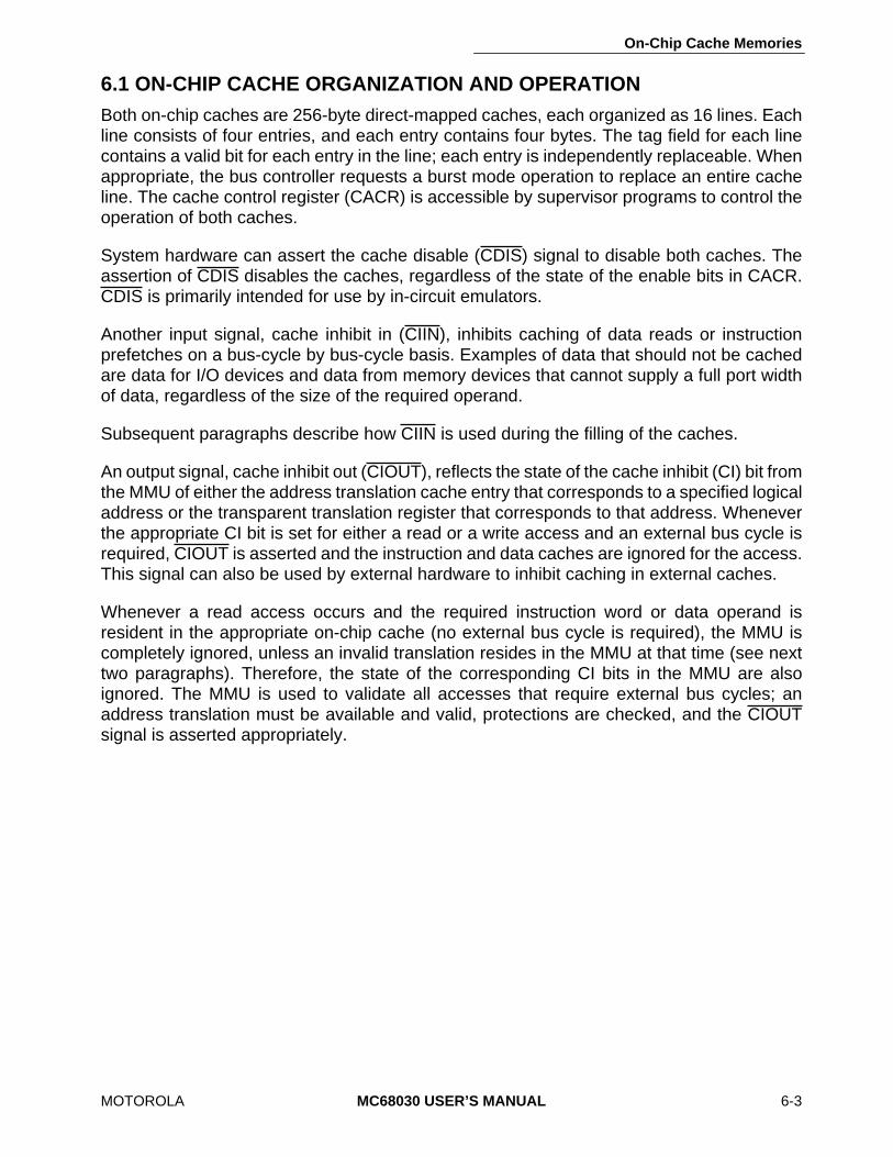
On-Chip Cache Memories
MOTOROLA
MC68030 USER’S MANUAL
6-3
6.1 ON-CHIP CACHE ORGANIZATION AND OPERATION
Both on-chip caches are 256-byte direct-mapped caches, each organized as 16 lines. Eachline consists of four entries, and each entry contains four bytes. The tag field for each linecontains a valid bit for each entry in the line; each entry is independently replaceable. Whenappropriate, the bus controller requests a burst mode operation to replace an entire cacheline. The cache control register (CACR) is accessible by supervisor programs to control theoperation of both caches.
System hardware can assert the cache disable (CDIS) signal to disable both caches. Theassertion of CDIS disables the caches, regardless of the state of the enable bits in CACR.CDIS is primarily intended for use by in-circuit emulators.
Another input signal, cache inhibit in (CIIN), inhibits caching of data reads or instructionprefetches on a bus-cycle by bus-cycle basis. Examples of data that should not be cachedare data for I/O devices and data from memory devices that cannot supply a full port widthof data, regardless of the size of the required operand.
Subsequent paragraphs describe how CIIN is used during the filling of the caches.
An output signal, cache inhibit out (CIOUT), reflects the state of the cache inhibit (CI) bit fromthe MMU of either the address translation cache entry that corresponds to a specified logicaladdress or the transparent translation register that corresponds to that address. Wheneverthe appropriate CI bit is set for either a read or a write access and an external bus cycle isrequired, CIOUT is asserted and the instruction and data caches are ignored for the access.This signal can also be used by external hardware to inhibit caching in external caches.
Whenever a read access occurs and the required instruction word or data operand isresident in the appropriate on-chip cache (no external bus cycle is required), the MMU iscompletely ignored, unless an invalid translation resides in the MMU at that time (see nexttwo paragraphs). Therefore, the state of the corresponding CI bits in the MMU are alsoignored. The MMU is used to validate all accesses that require external bus cycles; anaddress translation must be available and valid, protections are checked, and the CIOUTsignal is asserted appropriately.

On-Chip Cache Memories
6-4
MC68030 USER’S MANUAL
MOTOROLA
An external access is defined as “cachable” for either the instruction or data cache when allthe following conditions apply:
• The cache is enabled with the appropriate bit in the CACR set.
• The CDIS signal is negated.
• The CIIN signal is negated for the access.
• The CIOUT signal is negated for the access.
• The MMU validates the access.
Because both the data and instruction caches are referenced by logical addresses, theyshould be flushed during a task switch or at any time the logical-to-physical addressmapping changes, including when the MMU is first enabled. In addition, if a page descriptoris currently marked as valid and is later changed to the invalid type (due to a context switchor a page replacement operation)
entries in the on-chip instruction or data cachecorresponding to the physical page must be first cleared (invalidated)
. Otherwise, if on-chipcache entries are valid for pages with descriptors in memory marked invalid, processoroperation is unpredictable.
Data read and write accesses to the same address should also have consistent cachabilitystatus to ensure that the data in the cache remains consistent with external memory. Forexample, if CIOUT is negated for read accesses within a page and the MMU configurationis changed so that CIOUT is subsequently asserted for write accesses within the samepage, those write accesses do not update data in the cache, and stale data may result.Similarly, when the MMU maps multiple logical addresses to the same physical address, allaccesses to those logical addresses should have the same cachability status.
6.1.1 Instruction Cache
The instruction cache is organized with a line size of four long words, as shown in Figure 6-2. Each of these long words is considered a separate cache entry as each has a separatevalid bit. All four entries in a line have the same tag address. Burst filling all four long wordscan be advantageous when the time spent in filling the line is not long relative to theequivalent bus-cycle time for four nonburst long-word accesses, because of the probabilitythat the contents of memory adjacent to or close to a referenced operand or instruction isalso required by subsequent accesses. Dynamic RAMs supporting fast access modes(page, nibble, or static column) are easily employed to support the MC68030 burst mode.
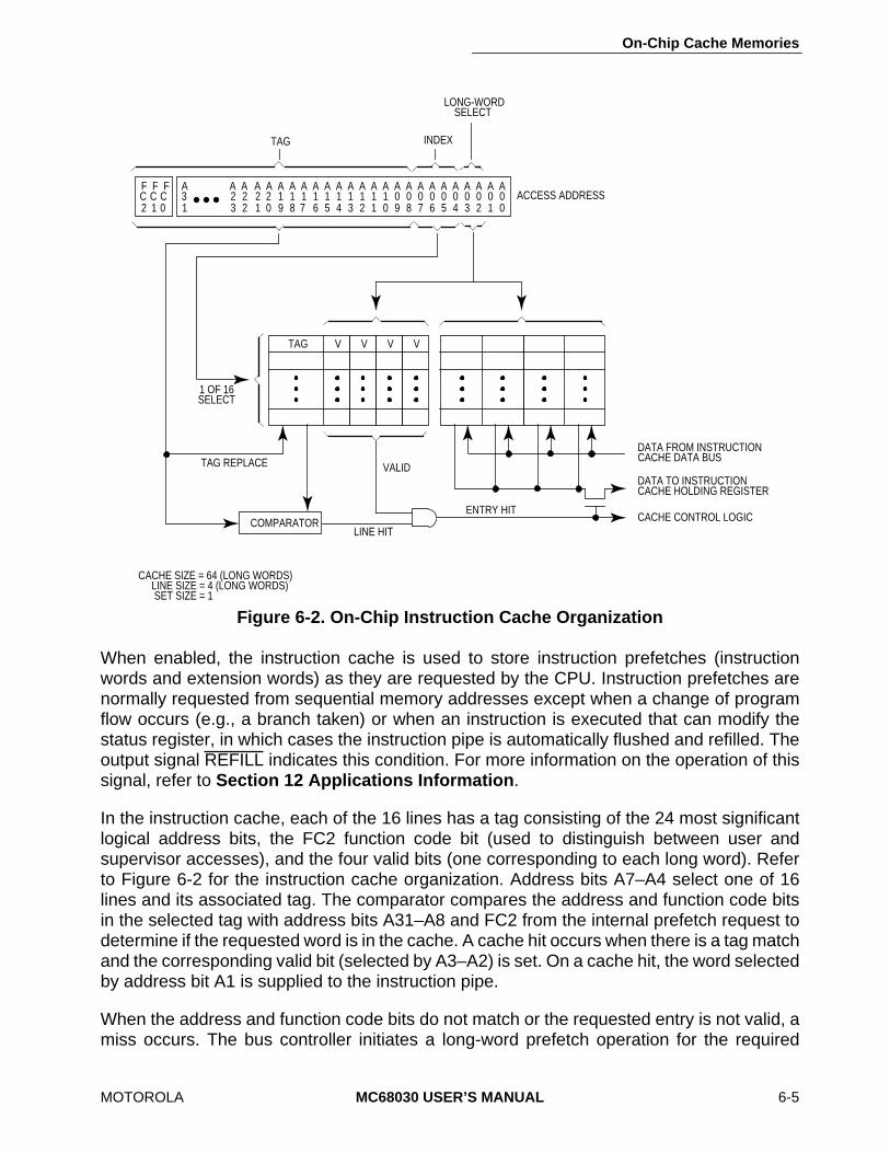
On-Chip Cache Memories
MOTOROLA
MC68030 USER’S MANUAL
6-5
When enabled, the instruction cache is used to store instruction prefetches (instructionwords and extension words) as they are requested by the CPU. Instruction prefetches arenormally requested from sequential memory addresses except when a change of programflow occurs (e.g., a branch taken) or when an instruction is executed that can modify thestatus register, in which cases the instruction pipe is automatically flushed and refilled. Theoutput signal REFILL indicates this condition. For more information on the operation of thissignal, refer to
Section 12 Applications Information
.
In the instruction cache, each of the 16 lines has a tag consisting of the 24 most significantlogical address bits, the FC2 function code bit (used to distinguish between user andsupervisor accesses), and the four valid bits (one corresponding to each long word). Referto Figure 6-2 for the instruction cache organization. Address bits A7–A4 select one of 16lines and its associated tag. The comparator compares the address and function code bitsin the selected tag with address bits A31–A8 and FC2 from the internal prefetch request todetermine if the requested word is in the cache. A cache hit occurs when there is a tag matchand the corresponding valid bit (selected by A3–A2) is set. On a cache hit, the word selectedby address bit A1 is supplied to the instruction pipe.
When the address and function code bits do not match or the requested entry is not valid, amiss occurs. The bus controller initiates a long-word prefetch operation for the required
Figure 6-2. On-Chip Instruction Cache Organization
F F FC C C 3 2 2 2 2 1 1 1 1 1 1 1 1 1 1 0 0 0 0 0 0 0 0 0 02 1 0 1 3 2 01 9 8 7 6 5 4 3 2 1 0 9 8 7 6 5 4 3 2 1 0
COMPARATOR
TAG
1 OF 16SELECT
VALIDTAG REPLACE
INDEXTAG
LINE HIT
DATA FROM INSTRUCTIONCACHE DATA BUS
CACHE CONTROL LOGIC
V V VV
ACCESS ADDRESS
DATA TO INSTRUCTIONCACHE HOLDING REGISTER
ENTRY HIT
A
LONG-WORDSELECT
CACHE SIZE = 64 (LONG WORDS) LINE SIZE = 4 (LONG WORDS) SET SIZE = 1
A A A A A A A A A A A A A A A A A A A A A A A A
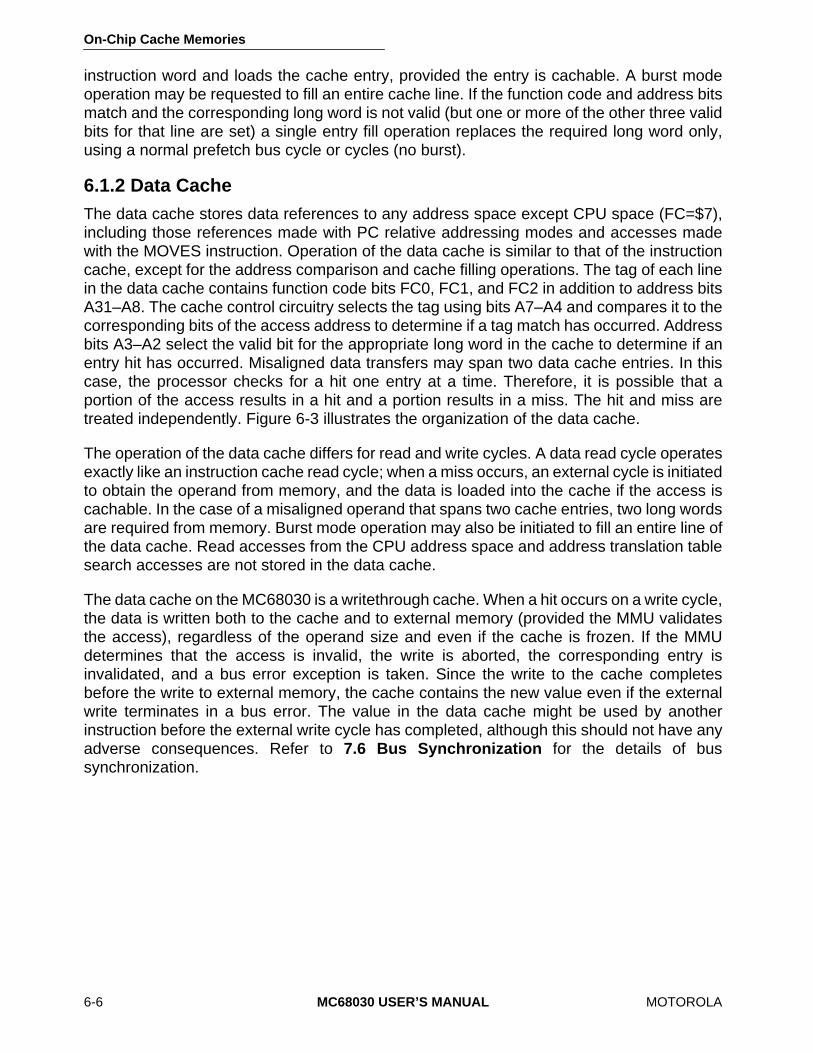
On-Chip Cache Memories
6-6
MC68030 USER’S MANUAL
MOTOROLA
instruction word and loads the cache entry, provided the entry is cachable. A burst modeoperation may be requested to fill an entire cache line. If the function code and address bitsmatch and the corresponding long word is not valid (but one or more of the other three validbits for that line are set) a single entry fill operation replaces the required long word only,using a normal prefetch bus cycle or cycles (no burst).
6.1.2 Data Cache
The data cache stores data references to any address space except CPU space (FC=$7),including those references made with PC relative addressing modes and accesses madewith the MOVES instruction. Operation of the data cache is similar to that of the instructioncache, except for the address comparison and cache filling operations. The tag of each linein the data cache contains function code bits FC0, FC1, and FC2 in addition to address bitsA31–A8. The cache control circuitry selects the tag using bits A7–A4 and compares it to thecorresponding bits of the access address to determine if a tag match has occurred. Addressbits A3–A2 select the valid bit for the appropriate long word in the cache to determine if anentry hit has occurred. Misaligned data transfers may span two data cache entries. In thiscase, the processor checks for a hit one entry at a time. Therefore, it is possible that aportion of the access results in a hit and a portion results in a miss. The hit and miss aretreated independently. Figure 6-3 illustrates the organization of the data cache.
The operation of the data cache differs for read and write cycles. A data read cycle operatesexactly like an instruction cache read cycle; when a miss occurs, an external cycle is initiatedto obtain the operand from memory, and the data is loaded into the cache if the access iscachable. In the case of a misaligned operand that spans two cache entries, two long wordsare required from memory. Burst mode operation may also be initiated to fill an entire line ofthe data cache. Read accesses from the CPU address space and address translation tablesearch accesses are not stored in the data cache.
The data cache on the MC68030 is a writethrough cache. When a hit occurs on a write cycle,the data is written both to the cache and to external memory (provided the MMU validatesthe access), regardless of the operand size and even if the cache is frozen. If the MMUdetermines that the access is invalid, the write is aborted, the corresponding entry isinvalidated, and a bus error exception is taken. Since the write to the cache completesbefore the write to external memory, the cache contains the new value even if the externalwrite terminates in a bus error. The value in the data cache might be used by anotherinstruction before the external write cycle has completed, although this should not have anyadverse consequences. Refer to
7.6 Bus Synchronization
for the details of bussynchronization.
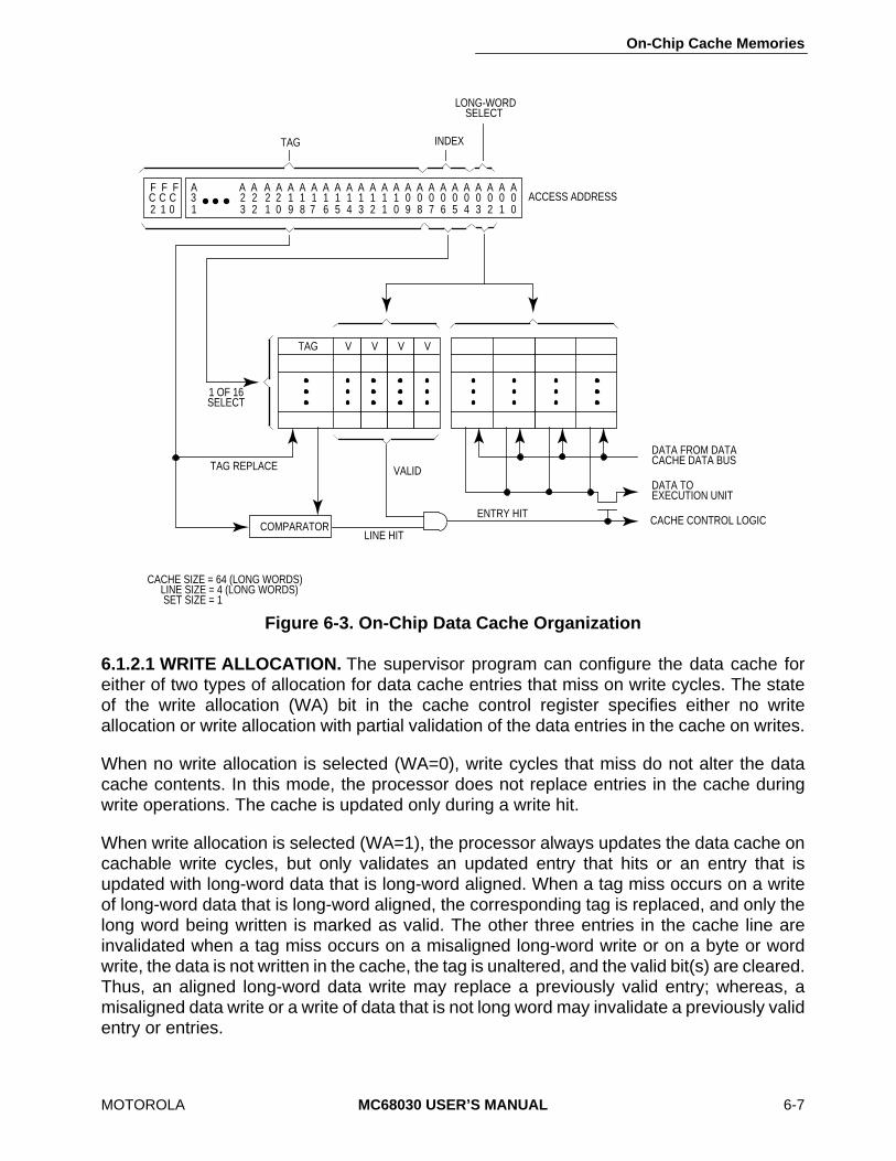
On-Chip Cache Memories
MOTOROLA
MC68030 USER’S MANUAL
6-7
6.1.2.1 WRITE ALLOCATION.
The supervisor program can configure the data cache foreither of two types of allocation for data cache entries that miss on write cycles. The stateof the write allocation (WA) bit in the cache control register specifies either no writeallocation or write allocation with partial validation of the data entries in the cache on writes.
When no write allocation is selected (WA=0), write cycles that miss do not alter the datacache contents. In this mode, the processor does not replace entries in the cache duringwrite operations. The cache is updated only during a write hit.
When write allocation is selected (WA=1), the processor always updates the data cache oncachable write cycles, but only validates an updated entry that hits or an entry that isupdated with long-word data that is long-word aligned. When a tag miss occurs on a writeof long-word data that is long-word aligned, the corresponding tag is replaced, and only thelong word being written is marked as valid. The other three entries in the cache line areinvalidated when a tag miss occurs on a misaligned long-word write or on a byte or wordwrite, the data is not written in the cache, the tag is unaltered, and the valid bit(s) are cleared.Thus, an aligned long-word data write may replace a previously valid entry; whereas, amisaligned data write or a write of data that is not long word may invalidate a previously validentry or entries.
Figure 6-3. On-Chip Data Cache Organization
DATA FROM DATACACHE DATA BUS
CACHE CONTROL LOGIC
DATA TOEXECUTION UNIT
F F FC C C 3 2 2 2 2 1 1 1 1 1 1 1 1 1 1 0 0 0 0 0 0 0 0 0 02 1 0 1 3 2 01 9 8 7 6 5 4 3 2 1 0 9 8 7 6 5 4 3 2 1 0
COMPARATOR
TAG
1 OF 16SELECT
VALIDTAG REPLACE
INDEXTAG
LINE HIT
V V VV
ACCESS ADDRESS
ENTRY HIT
A
LONG-WORDSELECT
CACHE SIZE = 64 (LONG WORDS) LINE SIZE = 4 (LONG WORDS) SET SIZE = 1
A A A A A A A A A A A A A A A A A A A A A A A A
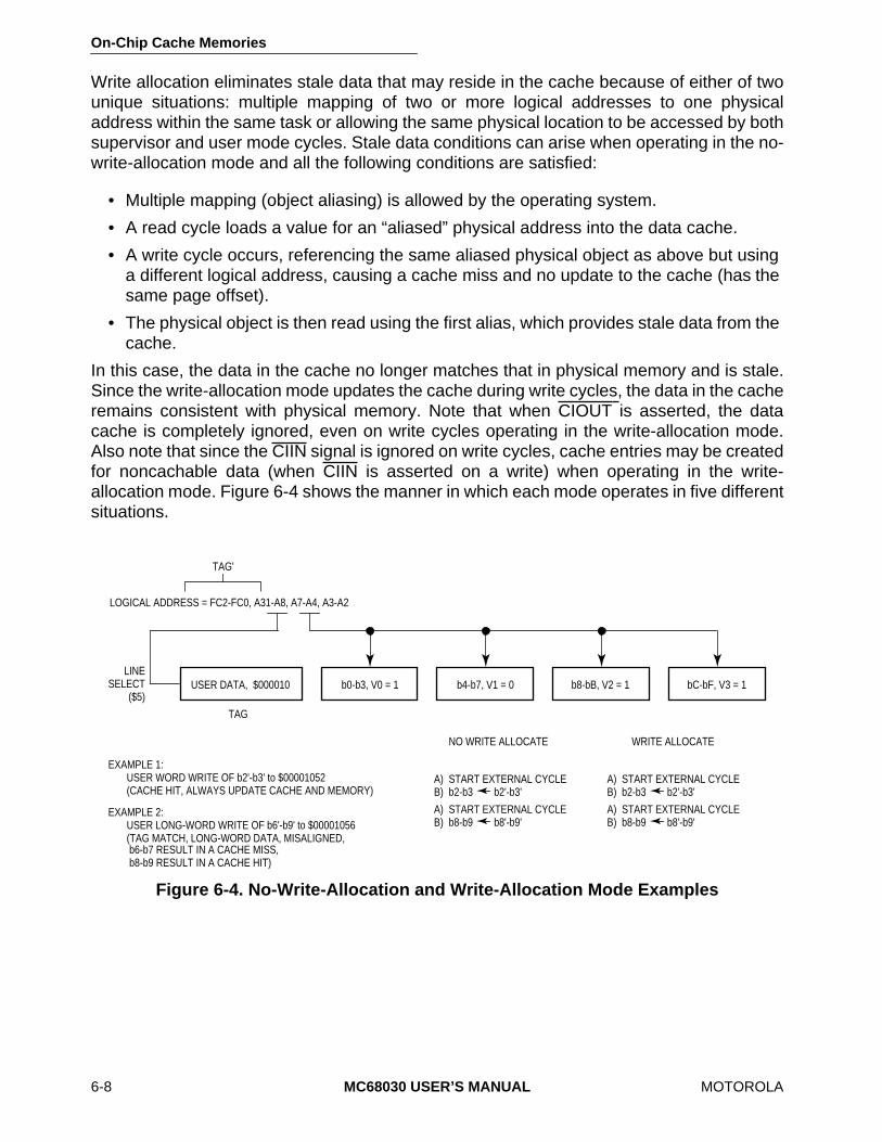
On-Chip Cache Memories
6-8
MC68030 USER’S MANUAL
MOTOROLA
Write allocation eliminates stale data that may reside in the cache because of either of twounique situations: multiple mapping of two or more logical addresses to one physicaladdress within the same task or allowing the same physical location to be accessed by bothsupervisor and user mode cycles. Stale data conditions can arise when operating in the no-write-allocation mode and all the following conditions are satisfied:
• Multiple mapping (object aliasing) is allowed by the operating system.
• A read cycle loads a value for an “aliased” physical address into the data cache.
• A write cycle occurs, referencing the same aliased physical object as above but using a different logical address, causing a cache miss and no update to the cache (has the same page offset).
• The physical object is then read using the first alias, which provides stale data from the cache.
In this case, the data in the cache no longer matches that in physical memory and is stale.Since the write-allocation mode updates the cache during write cycles, the data in the cacheremains consistent with physical memory. Note that when CIOUT is asserted, the datacache is completely ignored, even on write cycles operating in the write-allocation mode.Also note that since the CIIN signal is ignored on write cycles, cache entries may be createdfor noncachable data (when CIIN is asserted on a write) when operating in the write-allocation mode. Figure 6-4 shows the manner in which each mode operates in five differentsituations.
Figure 6-4. No-Write-Allocation and Write-Allocation Mode Examples
USER DATA, $000010 b0-b3, V0 = 1 b4-b7, V1 = 0 b8-bB, V2 = 1 bC-bF, V3 = 1LINE
SELECT($5)
LOGICAL ADDRESS = FC2-FC0, A31-A8, A7-A4, A3-A2
TAG'
TAG
EXAMPLE 1: USER WORD WRITE OF b2'-b3' to $00001052 (CACHE HIT, ALWAYS UPDATE CACHE AND MEMORY)
EXAMPLE 2: USER LONG-WORD WRITE OF b6'-b9' to $00001056 (TAG MATCH, LONG-WORD DATA, MISALIGNED, b6-b7 RESULT IN A CACHE MISS, b8-b9 RESULT IN A CACHE HIT)
A) START EXTERNAL CYCLE B) b2-b3 b2'-b3'
NO WRITE ALLOCATE
A) START EXTERNAL CYCLE B) b8-b9 b8'-b9'
A) START EXTERNAL CYCLE B) b2-b3 b2'-b3'
WRITE ALLOCATE
A) START EXTERNAL CYCLE B) b8-b9 b8'-b9'

On-Chip Cache Memories
MOTOROLA
MC68030 USER’S MANUAL
6-9
6.1.2.2 READ-MODIFY-WRITE ACCESSES.
The read portion of a read-modify-write cycleis always forced to miss in the data cache. However, if the system allows internal cachingof read-modify-write cycle operands (CIOUT and CIIN both negated), the processor eitheruses the data read from memory to update a matching entry in the data cache or creates anew entry with the read data in the case of no matching entry. The write portion of a read-modify-write operation also updates a matching entry in the data cache. In the case of acache miss on the write, the allocation of a new cache entry for the data being written iscontrolled by the WA bit. Table search accesses, however, are completely ignored by thedata cache; it is never updated for a table search access.
6.1.3 Cache Filling
The bus controller can load either cache in either of two ways:
• Single entry mode
• Burst fill mode
In the single entry mode, the bus controller loads a single long-word entry of a cache line.In the burst fill mode, an entire line (four long words) can be filled. Refer to
Section 7 BusOperation
for detailed information about the bus cycles required for both modes.
6.1.3.1 SINGLE ENTRY MODE.
When a cachable access is initiated and a burst modeoperation is not requested by the MC68030 or is not supported by external hardware, thebus controller transfers a single long word for the corresponding cache entry. An entire longword is required. If the port size of the responding device is smaller than 32 bits, theMC68030 executes all bus cycles necessary to fill the long word.
When a device cannot supply its entire port width of data, regardless of the size of thetransfer, the responding device must consistently assert the cache inhibit input (CIIN) signal.For example, a 32-bit port must always supply 32 bits, even for 8- and 16-bit transfers; a 16-bit port must supply 16 bits, even for 8-bit transfers. The MC68030 assumes that a 32-bittermination signal for the bus cycle indicates availability of 32 valid data bits, even if only 16or 8 bits are requested. Similarly, the processor assumes that a 16-bit termination signalindicates that all 16 bits are valid. If the device cannot supply its full port width of data, it mustassert CIIN for all bus cycles corresponding to a cache entry.
On-Chip Cache Memories
6-10
MC68030 USER’S MANUAL
MOTOROLA
When a cachable read cycle provides data with both CIIN and BERR negated, the MC68030attempts to fill the cache entry. Figure 6-5 shows the organization of a line of data in thecaches. The notation b0, b1, b2, and so forth identifies the bytes within the line. For eachentry in the line, a valid bit in the associated tag corresponds to a long-word entry to beloaded. Since a single valid bit applies to an entire long word, a single entry mode operationmust provide a full 32 bits of data. Ports less than 32 bits wide require several read cyclesfor each entry.
Figure 6-5 shows an example of a byte data operand read cycle starting at byte address $03from an 8-bit port. Provided the data item is cachable, this operation results in four buscycles. The first cycle requested by the MC68030 reads a byte from address $03. The 8-bitDSACKx response causes the MC68030 to fetch the remainder of the long word starting ataddress $00. The bytes are latched in the following order: b3, b0, b1, and b2. Note thatduring cache loading operations, devices must indicate the same port size consistentlythroughout all cycles for that long-word entry in the cache.
Figure 6-6 shows the access of a byte data operand from a 16-bit port. This operationrequires two read cycles. The first cycle requests the byte at address $03. If the deviceresponds with a 16-bit DSACKx encoding, the word at address $02 (including the requestedbyte) is accepted by the MC68030. The second cycle requests the word at address $00.Since the device again responds with a 16-bit DSACKx encoding, the remaining two bytesof the long word are latched, and the cache entry is filled.
With a 32-bit port, the same operation is shown in Figure 6-7. Only one read cycle isrequired. All four bytes (including the requested byte) are latched during the cycle.
If a requested access is misaligned and spans two cache entries, the bus controller attemptsto fill both associated long-word cache entries. An example of this is an operand request fora long word on an odd-word boundary. The MC68030 first fetches the initial byte(s) of theoperand (residing in the first long word) and then requests the remaining bytes to fill thatcache entry (if the port size is less than 32 bits) before it requests the remainder of theoperand and corresponding long word to fill the second cache entry. If the port size is 32bits, the processor performs two accesses, one for each cache entry.
(UNABLE TO LOCATE ART)
Figure 6-5. Single Entry Mode Operation — 8-Bit Port
(UNABLE TO LOCATE ART)
Figure 6-6. Single Entry Mode Operation — 16-Bit Port
(UNABLE TO LOCATE ART)
Figure 6-7. Single Entry Mode Operation — 32-Bit Port

On-Chip Cache Memories
MOTOROLA
MC68030 USER’S MANUAL
6-11
Figure 6-8 shows a misaligned access of a long word at address $06 from an 8-bit portrequiring eight bus cycles to complete. Reading this long-word operand requires eight readcycles, since accesses to all eight addresses return 8-bit port-size encodings. These cyclesfetch the two cache entries that the requested long-word spans. The first cycle requests along word at address $06 and accepts the first requested byte (b6). The subsequenttransfers of the first long word are performed in the following order: b7, b4, b5. Theremaining four read cycles transfer the four bytes of the second cache entry. The sequenceof access for the entire operation is b6, b7, b4, b5, b8, b9, bA, and bB.
The next example, shown in Figure 6-9, is a read of a misaligned long-word operand fromdevices that return 16-bit DSACKx encodings. The processor accepts the first portion of theoperand, the word from address $06, and requests a word from address $04 to fill the cacheentry. Next, the processor reads the word at address $08, the second portion of the operand,and stores it in the cache also. Finally, the processor accesses the word at $0A to fill thesecond long-word cache entry.
Two read cycles are required for a misaligned long-word operand transfer from devices thatreturn 32-bit DSACKx encodings. As shown in Figure 6-10, the first read cycle requests thelong word at address $06 and latches the long word at address $04. The second read cyclerequests and latches the long word corresponding to the second cache entry at address$08. Two read cycles are also required if STERM is used to indicate a 32-bit port instead ofthe 32-bit DSACKx encoding.
If all bytes of a long word are cachable, CIIN must be negated for all bus cycles required tofill the entry. If any byte is not cachable, CIIN must be asserted for all corresponding buscycles. The assertion of the CIIN signal prevents the caches from being updated during readcycles. Write cycles (including the write portion of a read-modify-write cycle) ignore theassertion of the CIIN signal and may cause the data cache to be altered, depending on thestate of the cache (whether or not the write cycle hits), the state of the WA bit in the CACR,and the conditions indicated by the MMU.
The occurrence of a bus error while attempting to load a cache entry aborts the entry filloperation but does not necessarily cause a bus error exception. If the bus error occurs on aread cycle for a portion of the required operand (not the remaining bytes of the cache entry)to be loaded into the data cache, the processor immediately takes a bus error exception. If
(UNABLE TO LOCATE ART)
Figure 6-8. Single Entry Mode Operation — Misaligned Long Word and 8-Bit Port
(UNABLE TO LOCATE ART)
Figure 6-9. Single Entry Mode Operation — Misaligned Long Word and 16-Bit Port
(UNABLE TO LOCATE ART)
Figure 6-10. Single Entry Mode Operation — Misaligned Long Word and 32-Bit DSACKx Port
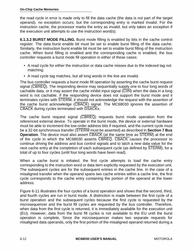
On-Chip Cache Memories
6-12
MC68030 USER’S MANUAL
MOTOROLA
the read cycle in error is made only to fill the data cache (the data is not part of the targetoperand), no exception occurs, but the corresponding entry is marked invalid. For theinstruction cache, the processor marks the entry as invalid, but only takes an exception ifthe execution unit attempts to use the instruction word(s).
6.1.3.2 BURST MODE FILLING.
Burst mode filling is enabled by bits in the cache controlregister. The data burst enable bit must be set to enable burst filling of the data cache.Similarly, the instruction burst enable bit must be set to enable burst filling of the instructioncache. When burst filling is enabled and the corresponding cache is enabled, the buscontroller requests a burst mode fill operation in either of these cases:
• A read cycle for either the instruction or data cache misses due to the indexed tag not matching.
• A read cycle tag matches, but all long words in the line are invalid.
The bus controller requests a burst mode fill operation by asserting the cache burst requestsignal (CBREQ). The responding device may sequentially supply one to four long words ofcachable data, or it may assert the cache inhibit input signal (CIIN) when the data in a longword is not cachable. If the responding device does not support the burst mode and itterminates cycles with STERM, it should not acknowledge the request with the assertion ofthe cache burst acknowledge (CBACK) signal. The MC68030 ignores the assertion ofCBACK during cycles terminated with DSACKx.
The cache burst request signal (CBREQ) requests burst mode operation from thereferenced external device. To operate in the burst mode, the device or external hardwaremust be able to increment the low-order address bits if required, and the current cycle mustbe a 32-bit synchronous transfer (STERM must be asserted) as described in
Section 7 BusOperation
. The device must also assert CBACK (at the same time as STERM) at the endof the cycle in which the MC68030 asserts CBREQ. CBACK causes the processor tocontinue driving the address and bus control signals and to latch a new data value for thenext cache entry at the completion of each subsequent cycle (as defined by STERM), for atotal of up to four cycles (until four long words have been read).
When a cache burst is initiated, the first cycle attempts to load the cache entrycorresponding to the instruction word or data item explicitly requested by the execution unit.The subsequent cycles are for the subsequent entries in the cache line. In the case of amisaligned transfer when the operand spans two cache entries within a cache line, the firstcycle corresponds to the cache entry containing the portion of the operand at the loweraddress.
Figure 6-11 illustrates the four cycles of a burst operation and shows that the second, third,and fourth cycles are run in burst mode. A distinction is made between the first cycle of aburst operation and the subsequent cycles because the first cycle is requested by themicrosequencer and the burst fill cycles are requested by the bus controller. Therefore,when data from the first cycle is returned, it is immediately available for the execution unit(EU). However, data from the burst fill cycles is not available to the EU until the burstoperation is complete. Since the microsequencer makes two separate requests formisaligned data operands, only the first portion of the misaligned operand returned during a
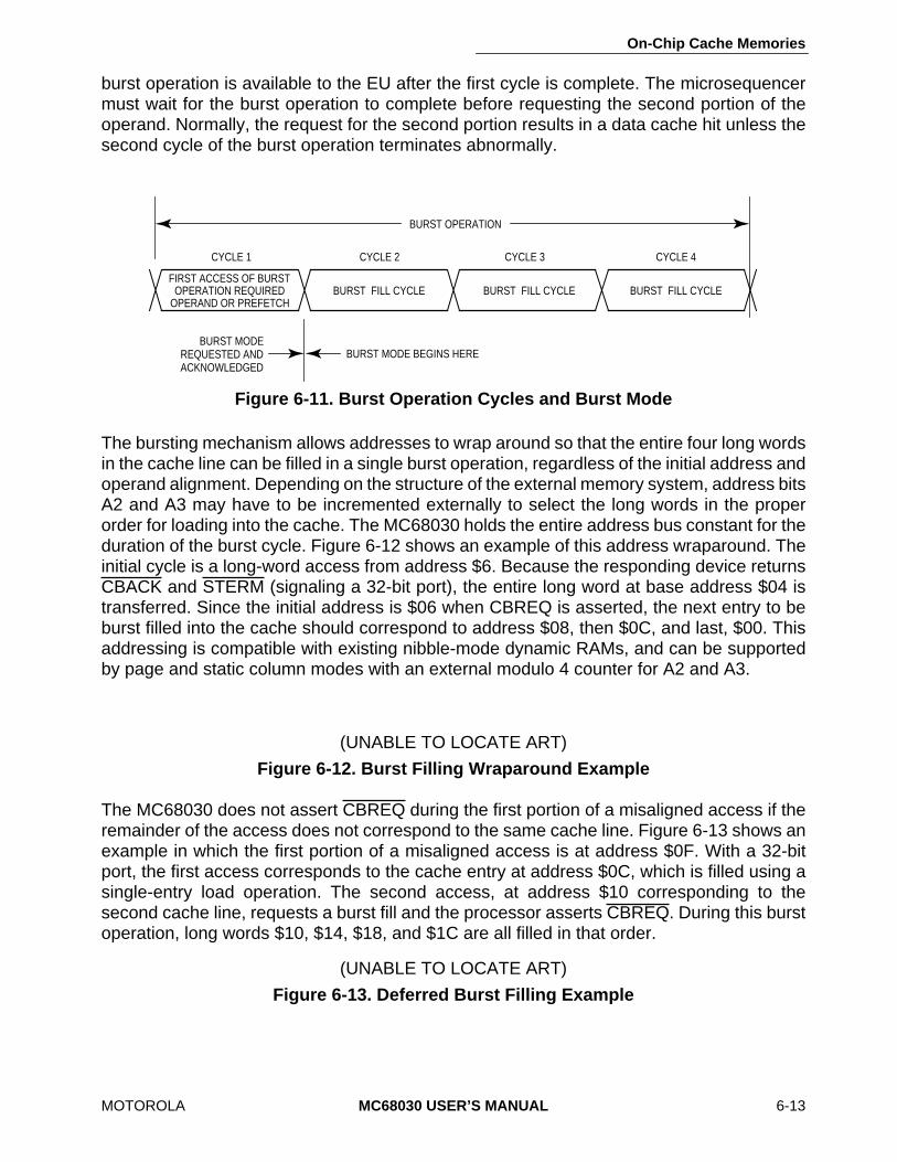
On-Chip Cache Memories
MOTOROLA
MC68030 USER’S MANUAL
6-13
burst operation is available to the EU after the first cycle is complete. The microsequencermust wait for the burst operation to complete before requesting the second portion of theoperand. Normally, the request for the second portion results in a data cache hit unless thesecond cycle of the burst operation terminates abnormally.
The bursting mechanism allows addresses to wrap around so that the entire four long wordsin the cache line can be filled in a single burst operation, regardless of the initial address andoperand alignment. Depending on the structure of the external memory system, address bitsA2 and A3 may have to be incremented externally to select the long words in the properorder for loading into the cache. The MC68030 holds the entire address bus constant for theduration of the burst cycle. Figure 6-12 shows an example of this address wraparound. Theinitial cycle is a long-word access from address $6. Because the responding device returnsCBACK and STERM (signaling a 32-bit port), the entire long word at base address $04 istransferred. Since the initial address is $06 when CBREQ is asserted, the next entry to beburst filled into the cache should correspond to address $08, then $0C, and last, $00. Thisaddressing is compatible with existing nibble-mode dynamic RAMs, and can be supportedby page and static column modes with an external modulo 4 counter for A2 and A3.
The MC68030 does not assert CBREQ during the first portion of a misaligned access if theremainder of the access does not correspond to the same cache line. Figure 6-13 shows anexample in which the first portion of a misaligned access is at address $0F. With a 32-bitport, the first access corresponds to the cache entry at address $0C, which is filled using asingle-entry load operation. The second access, at address $10 corresponding to thesecond cache line, requests a burst fill and the processor asserts CBREQ. During this burstoperation, long words $10, $14, $18, and $1C are all filled in that order.
Figure 6-11. Burst Operation Cycles and Burst Mode
(UNABLE TO LOCATE ART)
Figure 6-12. Burst Filling Wraparound Example
(UNABLE TO LOCATE ART)
Figure 6-13. Deferred Burst Filling Example
FIRST ACCESS OF BURSTOPERATION REQUIRED
OPERAND OR PREFETCHBURST FILL CYCLE BURST FILL CYCLE BURST FILL CYCLE
CYCLE 1 CYCLE 2 CYCLE 3 CYCLE 4
BURST MODEREQUESTED ANDACKNOWLEDGED
BURST MODE BEGINS HERE
BURST OPERATION
On-Chip Cache Memories
6-14
MC68030 USER’S MANUAL
MOTOROLA
The processor does not assert CBREQ if any of the following conditions exist:
• The appropriate cache is not enabled
• Burst filling for the cache is not enabled
• The cache freeze bit for the appropriate cache is set
• The current operation is the read portion of a read-modify-write operation
• The MMU has inhibited caching for the current page
• The cycle is for the first access of an operand that spans two cache lines (crosses a modulo 16 boundary)
Additionally, the assertion of CIIN and BERR and the premature negation of CBACK affectburst operation as described in the following paragraphs.
The assertion of CIIN during the first cycle of a burst operation causes the data to be latchedby the processor, and if the requested operand is aligned (the entire operand is latched inthe first cycle), the data is passed on to the instruction pipe or execution unit. However, thedata is not loaded into its corresponding cache. In addition, the MC68030 negates CBREQ,and the burst operation is aborted. If a portion of the requested operand remains to be read(due to misalignment), a second read cycle is initiated at the appropriate address withCBREQ negated.
The assertion of CIIN during the second, third, or fourth cycle of a burst operation preventsthe data during that cycle from being loaded into the appropriate cache and causes CBREQto negate, aborting the burst operation. However, if the data for the cycle contains part ofthe requested operand, the execution unit uses that data.
The premature negation of the CBACK signal during the burst operation causes the currentcycle to complete normally, loading the data successfully transferred into the appropriatecache. However, the burst operation aborts and CBREQ negates.
A bus error occurring during a burst operation also causes the burst operation to abort. If thebus error occurs during the first cycle of a burst (i.e., before burst mode is entered), the dataread from the bus is ignored, and the entire associated cache line is marked “invalid”. If theaccess is a data cycle, exception processing proceeds immediately. If the cycle is for aninstruction fetch, a bus error exception is made pending. This bus error is processed only ifthe execution unit attempts to use either instruction word. Refer to
11.2.2 Instruction Pipe
for more information about pipeline operation.
For either cache, when a bus error occurs after the burst mode has been entered (that is,on the second cycle or later), the cache entry corresponding to that cycle is marked invalid,but the processor does not take an exception (the microsequencer has not yet requestedthe data). In the case of an instruction cache burst, the data from the aborted cycle iscompletely ignored. Pending instruction prefetches are still pending and are subsequentlyrun by the processor. If the second cycle is for a portion of a misaligned data operand fetchand a bus error occurs, the processor terminates the burst operation and negates CBREQ.Once the burst terminates, the microsequencer requests a read cycle for the second portion.Since the burst terminated abnormally for the second cycle of the burst, the data cache
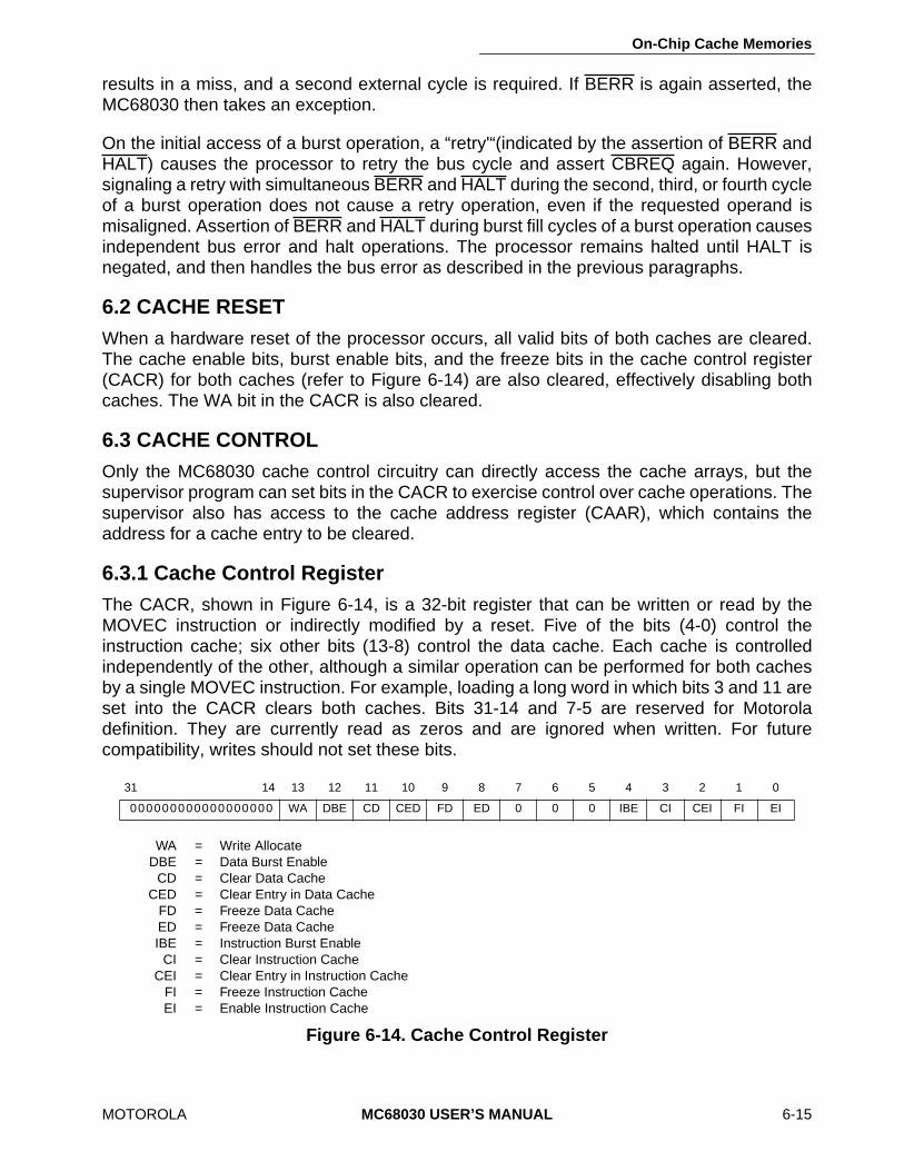
On-Chip Cache Memories
MOTOROLA
MC68030 USER’S MANUAL
6-15
results in a miss, and a second external cycle is required. If BERR is again asserted, theMC68030 then takes an exception.
On the initial access of a burst operation, a “retry'“(indicated by the assertion of BERR andHALT) causes the processor to retry the bus cycle and assert CBREQ again. However,signaling a retry with simultaneous BERR and HALT during the second, third, or fourth cycleof a burst operation does not cause a retry operation, even if the requested operand ismisaligned. Assertion of BERR and HALT during burst fill cycles of a burst operation causesindependent bus error and halt operations. The processor remains halted until HALT isnegated, and then handles the bus error as described in the previous paragraphs.
6.2 CACHE RESET
When a hardware reset of the processor occurs, all valid bits of both caches are cleared.The cache enable bits, burst enable bits, and the freeze bits in the cache control register(CACR) for both caches (refer to Figure 6-14) are also cleared, effectively disabling bothcaches. The WA bit in the CACR is also cleared.
6.3 CACHE CONTROL
Only the MC68030 cache control circuitry can directly access the cache arrays, but thesupervisor program can set bits in the CACR to exercise control over cache operations. Thesupervisor also has access to the cache address register (CAAR), which contains theaddress for a cache entry to be cleared.
6.3.1 Cache Control Register
The CACR, shown in Figure 6-14, is a 32-bit register that can be written or read by theMOVEC instruction or indirectly modified by a reset. Five of the bits (4-0) control theinstruction cache; six other bits (13-8) control the data cache. Each cache is controlledindependently of the other, although a similar operation can be performed for both cachesby a single MOVEC instruction. For example, loading a long word in which bits 3 and 11 areset into the CACR clears both caches. Bits 31-14 and 7-5 are reserved for Motoroladefinition. They are currently read as zeros and are ignored when written. For futurecompatibility, writes should not set these bits.
WA = Write AllocateDBE = Data Burst Enable
CD = Clear Data CacheCED = Clear Entry in Data Cache
FD = Freeze Data CacheED = Freeze Data CacheIBE = Instruction Burst Enable
CI = Clear Instruction CacheCEI = Clear Entry in Instruction Cache
FI = Freeze Instruction CacheEI = Enable Instruction Cache
Figure 6-14. Cache Control Register
31 14 13 12 11 10 9 8 7 6 5 4 3 2 1 0
000000000000000000 WA DBE CD CED FD ED 0 0 0 IBE CI CEI FI EI

On-Chip Cache Memories
6-16
MC68030 USER’S MANUAL
MOTOROLA
6.3.1.1 WRITE ALLOCATE.
Bit 13, the WA bit, is set to select the write-allocation mode(refer to
6.1.2.1 Write Allocation
) for write cycles. Clearing this bit selects the no-write-allocation mode. A reset operation clears this bit. The supervisor should set this bit when itshares data with the user task or when any task maps multiple logical addresses to onephysical address. If the data cache is disabled or frozen, the WA bit is ignored.
6.3.1.2 DATA BURST ENABLE.
Bit 12, the DBE bit, is set to enable burst filling of the datacache. Operating systems and other software set this bit when burst filling of the data cacheis desired. A reset operation clears the DBE bit.
6.3.1.3 CLEAR DATA CACHE.
Bit 11, the CD bit, is set to clear all entries in the data cache.Operating systems and other software set this bit to clear data from the cache prior to acontext switch. The processor clears all valid bits in the data cache at the time a MOVECinstruction loads a one into the CD bit of the CACR. The CD bit is always read as a zero.
6.3.1.4 CLEAR ENTRY IN DATA CACHE.
Bit 10, the CED bit, is set to clear an entry in thedata cache. The index field of the CAAR (see Figure 6-15) corresponding to the index andlong-word select portion of an address specifies the entry to be cleared. The processorclears only the specified long word by clearing the valid bit for the entry at the time a MOVECinstruction loads a one into the CED bit of the CACR, regardless of the states of the ED andFD bits. The CED bit is always read as a zero.
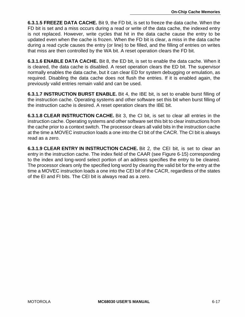
On-Chip Cache Memories
MOTOROLA
MC68030 USER’S MANUAL
6-17
6.3.1.5 FREEZE DATA CACHE.
Bit 9, the FD bit, is set to freeze the data cache. When theFD bit is set and a miss occurs during a read or write of the data cache, the indexed entryis not replaced. However, write cycles that hit in the data cache cause the entry to beupdated even when the cache is frozen. When the FD bit is clear, a miss in the data cacheduring a read cycle causes the entry (or line) to be filled, and the filling of entries on writesthat miss are then controlled by the WA bit. A reset operation clears the FD bit.
6.3.1.6 ENABLE DATA CACHE.
Bit 8, the ED bit, is set to enable the data cache. When itis cleared, the data cache is disabled. A reset operation clears the ED bit. The supervisornormally enables the data cache, but it can clear ED for system debugging or emulation, asrequired. Disabling the data cache does not flush the entries. If it is enabled again, thepreviously valid entries remain valid and can be used.
6.3.1.7 INSTRUCTION BURST ENABLE.
Bit 4, the IBE bit, is set to enable burst filling ofthe instruction cache. Operating systems and other software set this bit when burst filling ofthe instruction cache is desired. A reset operation clears the IBE bit.
6.3.1.8 CLEAR INSTRUCTION CACHE.
Bit 3, the CI bit, is set to clear all entries in theinstruction cache. Operating systems and other software set this bit to clear instructions fromthe cache prior to a context switch. The processor clears all valid bits in the instruction cacheat the time a MOVEC instruction loads a one into the CI bit of the CACR. The CI bit is alwaysread as a zero.
6.3.1.9 CLEAR ENTRY IN INSTRUCTION CACHE.
Bit 2, the CEI bit, is set to clear anentry in the instruction cache. The index field of the CAAR (see Figure 6-15) correspondingto the index and long-word select portion of an address specifies the entry to be cleared.The processor clears only the specified long word by clearing the valid bit for the entry at thetime a MOVEC instruction loads a one into the CEI bit of the CACR, regardless of the statesof the EI and FI bits. The CEI bit is always read as a zero.
On-Chip Cache Memories
6-18
MC68030 USER’S MANUAL
MOTOROLA
6.3.1.10 FREEZE INSTRUCTION CACHE.
Bit 1, the FI bit, is set to freeze the instructioncache. When the FI bit is set and a miss occurs in the instruction cache, the entry (or line)is not replaced. When the FI bit is cleared to zero, a miss in the instruction cache causes theentry (or line) to be filled. A reset operation clears the FI bit.
6.3.1.11 ENABLE INSTRUCTION CACHE.
Bit 0, the EI bit, is set to enable the instructioncache. When it is cleared, the instruction cache is disabled. A reset operation clears the EIbit. The supervisor normally enables the instruction cache, but it can clear EI for systemdebugging or emulation, as required. Disabling the instruction cache does not flush theentries. If it is enabled again, the previously valid entries remain valid and may be used.
6.3.2 Cache Address Register
The CAAR is a 32-bit register shown in Figure 6-15. The index field (bits 7-2) contains theaddress for the “clear cache entry” operations. The bits of this field correspond to bits 7-2 ofaddresses; they specify the index and a long word of a cache line. Although only the indexfield is used currently, all 32 bits of the register are implemented and are reserved for useby Motorola.
Figure 6-15. Cache Address Register
31 8 7 2 1 0CACHE FUNCTION ADDRESS INDEX
MOTOROLA
MC68030 USER’S MANUAL
7-1
SECTION 7BUS OPERATION
This section provides a functional description of the bus, the signals that control it, and thebus cycles provided for data transfer operations. It also describes the error and haltconditions, bus arbitration, and the reset operation. Operation of the bus is the samewhether the processor or an external device is the bus master; the names and descriptionsof bus cycles are from the point of view of the bus master. For exact timing specifications,refer to
Section 13 Electrical Characteristics
.
The MC68030 architecture supports byte, word, and long-word operands, allowing accessto 8-, 16-, and 32-bit data ports through the use of asynchronous cycles controlled by thedata transfer and size acknowledge inputs (DSACK0 and DSACK1).
Synchronous bus cycles controlled by the synchronous termination signal (STERM) canonly be used to transfer data to and from 32-bit ports.
The MC68030 allows byte, word, and long-word operands to be located in memory on anybyte boundary. For a misaligned transfer, more than one bus cycle may be required tocomplete the transfer, regardless of port size. For a port less than 32 bits wide, multiple buscycles may be required for an operand transfer due to either misalignment or a port widthsmaller than the operand size. Instruction words and their associated extension words mustbe aligned on word boundaries. The user should be aware that misalignment of word orlong-word operands can cause the MC68030 to perform multiple bus cycles for the operandtransfer; therefore, processor performance is optimized if word and long-word memoryoperands are aligned on word or long-word boundaries, respectively.
7.1 BUS TRANSFER SIGNALS
The bus transfers information between the MC68030 and an external memory, coprocessor,or peripheral device. External devices can accept or provide 8 bits, 16 bits, or 32 bits inparallel and must follow the handshake protocol described in this section. The maximumnumber of bits accepted or provided during a bus transfer is defined as the port width. TheMC68030 contains an address bus that specifies the address for the transfer and a data busthat transfers the data. Control signals indicate the beginning of the cycle, the address spaceand the size of the transfer, and the type of cycle. The selected device then controls thelength of the cycle with the signal(s) used to terminate the cycle. Strobe signals, one for theaddress bus and another for the data bus, indicate the validity of the address and providetiming information for the data.
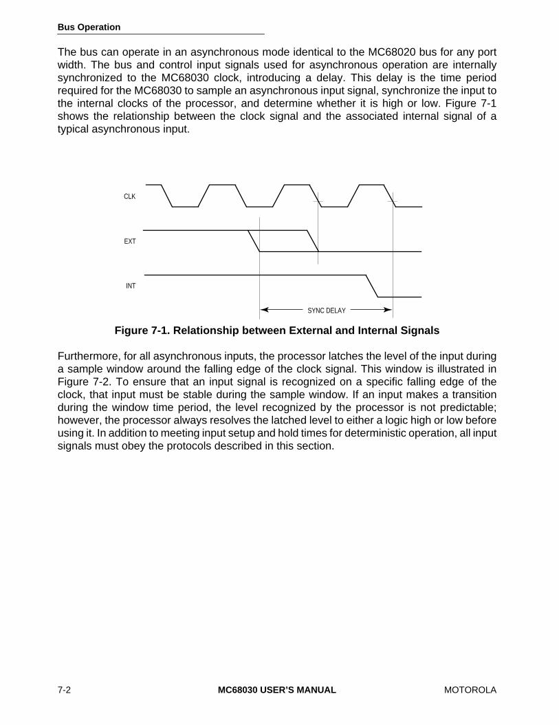
Bus Operation
7-2
MC68030 USER’S MANUAL
MOTOROLA
The bus can operate in an asynchronous mode identical to the MC68020 bus for any portwidth. The bus and control input signals used for asynchronous operation are internallysynchronized to the MC68030 clock, introducing a delay. This delay is the time periodrequired for the MC68030 to sample an asynchronous input signal, synchronize the input tothe internal clocks of the processor, and determine whether it is high or low. Figure 7-1shows the relationship between the clock signal and the associated internal signal of atypical asynchronous input.
Furthermore, for all asynchronous inputs, the processor latches the level of the input duringa sample window around the falling edge of the clock signal. This window is illustrated inFigure 7-2. To ensure that an input signal is recognized on a specific falling edge of theclock, that input must be stable during the sample window. If an input makes a transitionduring the window time period, the level recognized by the processor is not predictable;however, the processor always resolves the latched level to either a logic high or low beforeusing it. In addition to meeting input setup and hold times for deterministic operation, all inputsignals must obey the protocols described in this section.
Figure 7-1. Relationship between External and Internal Signals
SYNC DELAY
CLK
EXT
INT
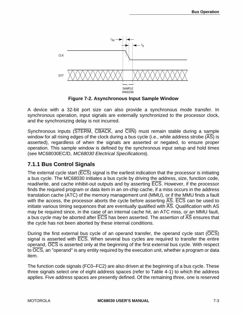
Bus Operation
MOTOROLA
MC68030 USER’S MANUAL
7-3
A device with a 32-bit port size can also provide a synchronous mode transfer. Insynchronous operation, input signals are externally synchronized to the processor clock,and the synchronizing delay is not incurred.
Synchronous inputs (STERM, CBACK, and CIIN) must remain stable during a samplewindow for all rising edges of the clock during a bus cycle (i.e., while address strobe (AS) isasserted), regardless of when the signals are asserted or negated, to ensure properoperation. This sample window is defined by the synchronous input setup and hold times(see MC68030EC/D,
MC68030 Electrical Specifications
).
7.1.1 Bus Control Signals
The external cycle start (ECS) signal is the earliest indication that the processor is initiatinga bus cycle. The MC68030 initiates a bus cycle by driving the address, size, function code,read/write, and cache inhibit-out outputs and by asserting ECS. However, if the processorfinds the required program or data item in an on-chip cache, if a miss occurs in the addresstranslation cache (ATC) of the memory management unit (MMU), or if the MMU finds a faultwith the access, the processor aborts the cycle before asserting AS. ECS can be used toinitiate various timing sequences that are eventually qualified with AS. Qualification with ASmay be required since, in the case of an internal cache hit, an ATC miss, or an MMU fault,a bus cycle may be aborted after ECS has been asserted. The assertion of AS ensures thatthe cycle has not been aborted by these internal conditions.
During the first external bus cycle of an operand transfer, the operand cycle start (OCS)signal is asserted with ECS. When several bus cycles are required to transfer the entireoperand, OCS is asserted only at the beginning of the first external bus cycle. With respectto OCS, an "operand'' is any entity required by the execution unit, whether a program or dataitem.
The function code signals (FC0–FC2) are also driven at the beginning of a bus cycle. Thesethree signals select one of eight address spaces (refer to Table 4-1) to which the addressapplies. Five address spaces are presently defined. Of the remaining three, one is reserved
Figure 7-2. Asynchronous Input Sample Window
t su
th
SAMPLEWINDOW
CLK
EXT
Bus Operation
7-4
MC68030 USER’S MANUAL
MOTOROLA
for user definition and two are reserved by Motorola for future use. The function code signalsare valid while AS is asserted.
At the beginning of a bus cycle, the size signals (SIZ0 and SIZ1) are driven along with ECSand the FC0–FC2. SIZ0 and SIZ1 indicate the number of bytes remaining to be transferredduring an operand cycle (consisting of one or more bus cycles) or during a cache filloperation from a device with a port size that is less than 32 bits. Table 7-2 shows theencoding of SIZ0 and SIZ1. These signals are valid while AS is asserted.
The read/write (R/W) signal determines the direction of the transfer during a bus cycle. Thissignal changes state, when required, at the beginning of a bus cycle and is valid while ASis asserted. R/W only transitions when a write cycle is preceded by a read cycle or viceversa. The signal may remain low for two consecutive write cycles.
The read-modify-write cycle signal (RMC) is asserted at the beginning of the first bus cycleof a read-modify-write operation and remains asserted until completion of the final bus cycleof the operation. The RMC signal is guaranteed to be negated before the end of state 0 fora bus cycle following a read-modify-write operation.
7.1.2 Address Bus
The address bus signals (A0–A31) define the address of the byte (or the most significantbyte) to be transferred during a bus cycle. The processor places the address on the bus atthe beginning of a bus cycle. The address is valid while AS is asserted.
7.1.3 Address Strobe
AS is a timing signal that indicates the validity of an address on the address bus and of manycontrol signals. It is asserted one-half clock after the beginning of a bus cycle.

Bus Operation
MOTOROLA
MC68030 USER’S MANUAL
7-5
7.1.4 Data Bus
The data bus signals (D0–D31) comprise a bidirectional, nonmultiplexed parallel bus thatcontains the data being transferred to or from the processor. A read or write operation maytransfer 8, 16, 24, or 32 bits of data (one, two, three, or four bytes) in one bus cycle. Duringa read cycle, the data is latched by the processor on the last falling edge of the clock for thatbus cycle. For a write cycle, all 32 bits of the data bus are driven, regardless of the port widthor operand size. The processor places the data on the data bus one-half clock cycle afterAS is asserted in a write cycle.
7.1.5 Data Strobe
The data strobe (DS) is a timing signal that applies to the data bus. For a read cycle, theprocessor asserts DS to signal the external device to place data on the bus. It is asserted atthe same time as AS during a read cycle. For a write cycle, DS signals to the external devicethat the data to be written is valid on the bus. The processor asserts DS one full clock cycleafter the assertion of AS during a write cycle.
7.1.6 Data Buffer Enable
The data buffer enable signal (DBEN) can be used to enable external data buffers while datais present on the data bus. During a read operation, DBEN is asserted one clock cycle afterthe beginning of the bus cycle and is negated as DS is negated. In a write operation, DBENis asserted at the time AS is asserted and is held active for the duration of the cycle. In asynchronous system supporting two-clock bus cycles, DBEN timing may prevent its use.
7.1.7 Bus Cycle Termination Signals
During asynchronous bus cycles, external devices assert the data transfer and sizeacknowledge signals (DSACK0 and/or DSACK1) as part of the bus protocol. During a readcycle, the assertion of DSACKx signals the processor to terminate the bus cycle and to latchthe data. During a write cycle, the assertion of DSACKx indicates that the external devicehas successfully stored the data and that the cycle may terminate. These signals alsoindicate to the processor the size of the port for the bus cycle just completed, as shown inTable 7-1. Refer to
7.3.1 Asynchronous Read Cycle
for timing relationships of DSACK0and DSACK1.
Bus Operation
7-6
MC68030 USER’S MANUAL
MOTOROLA
For synchronous bus cycles, external devices assert the synchronous termination signal(STERM) as part of the bus protocol. During a read cycle, the assertion of STERM causesthe processor to latch the data. During a write cycle, it indicates that the external device hassuccessfully stored the data. In either case, it terminates the cycle and indicates that thetransfer was made to a 32-bit port. Refer to
7.3.2 Asynchronous Write Cycle
for timingrelationships of STERM.
The bus error (BERR) signal is also a bus cycle termination indicator and can be used in theabsence of DSACKx or STERM to indicate a bus error condition. It can also be asserted inconjunction with DSACKx or STERM to indicate a bus error condition, provided it meets theappropriate timing described in this section and in MC68030EC/D,
MC68030 ElectricalSpecifications
. Additionally, the BERR and HALT signals can be asserted together toindicate a retry termination. Again, the BERR and HALT signals can be assertedsimultaneously in lieu of or in conjunction with the DSACKx or STERM signals.
Finally, the autovector (AVEC) signal can be used to terminate interrupt acknowledgecycles, indicating that the MC68030 should internally generate a vector number to locate aninterrupt handler routine. AVEC is ignored during all other bus cycles.
7.2 DATA TRANSFER MECHANISM
The MC68030 architecture supports byte, word, and long-word operands allowing accessto 8-, 16-, and 32-bit data ports through the use of asynchronous cycles controlled byDSACK0 and DSACK1. It also supports synchronous bus cycles to and from 32-bit ports,terminated by STERM. Byte, word, and long-word operands can be located on any byteboundary, but misaligned transfers may require additional bus cycles, regardless of portsize.
When the processor requests a burst mode fill operation, it asserts the cache burst request(CBREQ) signal to attempt to fill four entries within a line in one of the on-chip caches. Thismode is compatible with nibble, static column, or page mode dynamic RAMs. The burst filloperation uses synchronous bus cycles, each terminated by STERM, to fetch as many asfour long words.
7.2.1 Dynamic Bus Sizing
The MC68030 dynamically interprets the port size of the addressed device during each buscycle, allowing operand transfers to or from 8-, 16-, and 32-bit ports. During anasynchronous operand transfer cycle, the slave device signals its port size (byte, word, orlong word) and indicates completion of the bus cycle to the processor through the use of theDSACKx inputs. Refer to Table 7-1 for DSACKx encodings and assertion results.

Bus Operation
MOTOROLA
MC68030 USER’S MANUAL
7-7
For example, if the processor is executing an instruction that reads a long-word operandfrom a long-word aligned address, it attempts to read 32 bits during the first bus cycle. (Referto
7.2.2 Misaligned Operands
for the case of a word or byte address.) If the port respondsthat it is 32 bits wide, the MC68030 latches all 32 bits of data and continues with the nextoperation. If the port responds that it is 16 bits wide, the MC68030 latches the 16 bits of validdata and runs another bus cycle to obtain the other 16 bits. The operation for an 8-bit portis similar, but requires four read cycles. The addressed device uses the DSACKx signals toindicate the port width. For instance, a 32-bit device
always
returns DSACKx for a 32-bit port(regardless of whether the bus cycle is a byte, word, or long-word operation).
Dynamic bus sizing requires that the portion of the data bus used for a transfer to or from aparticular port size be fixed. A 32-bit port must reside on data bus bits 0–31, a 16-bit portmust reside on data bus bits 16-32, and an 8-bit port must reside on data bus bits 24-31.This requirement minimizes the number of bus cycles needed to transfer data to 8- and 16-bit ports and ensures that the MC68030 correctly transfers valid data. The MC68030 alwaysattempts to transfer the maximum amount of data on all bus cycles; for a long-wordoperation, it always assumes that the port is 32 bit wide when beginning the bus cycle.
The bytes of operands are designated as shown in Figure 7-3. The most significant byte ofa long-word operand is OP0, and OP3 is the least significant byte. The two bytes of a word-length operand are OP2 (most significant) and OP3. The single byte of a byte-lengthoperand is OP3. These designations are used in the figures and descriptions that follow.
Table 7-1. DSACK Codes and Results
DSACK1 DSACK0
Result
H H Insert Wait States in Current Bus Cycle
H L Complete Cycle — Data Bus Port Size is 8 Bits
L H Complete Cycle — Data Bus Port Size is 16 Bits
L L Complete Cycle — Data Bus Port Size is 32 Bits
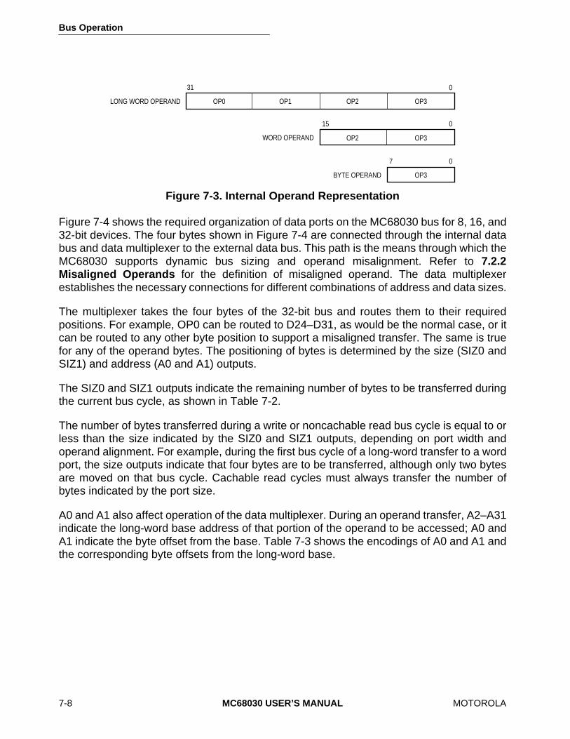
Bus Operation
7-8
MC68030 USER’S MANUAL
MOTOROLA
Figure 7-4 shows the required organization of data ports on the MC68030 bus for 8, 16, and32-bit devices. The four bytes shown in Figure 7-4 are connected through the internal databus and data multiplexer to the external data bus. This path is the means through which theMC68030 supports dynamic bus sizing and operand misalignment. Refer to
7.2.2Misaligned Operands
for the definition of misaligned operand. The data multiplexerestablishes the necessary connections for different combinations of address and data sizes.
The multiplexer takes the four bytes of the 32-bit bus and routes them to their requiredpositions. For example, OP0 can be routed to D24–D31, as would be the normal case, or itcan be routed to any other byte position to support a misaligned transfer. The same is truefor any of the operand bytes. The positioning of bytes is determined by the size (SIZ0 andSIZ1) and address (A0 and A1) outputs.
The SIZ0 and SIZ1 outputs indicate the remaining number of bytes to be transferred duringthe current bus cycle, as shown in Table 7-2.
The number of bytes transferred during a write or noncachable read bus cycle is equal to orless than the size indicated by the SIZ0 and SIZ1 outputs, depending on port width andoperand alignment. For example, during the first bus cycle of a long-word transfer to a wordport, the size outputs indicate that four bytes are to be transferred, although only two bytesare moved on that bus cycle. Cachable read cycles must always transfer the number ofbytes indicated by the port size.
A0 and A1 also affect operation of the data multiplexer. During an operand transfer, A2–A31indicate the long-word base address of that portion of the operand to be accessed; A0 andA1 indicate the byte offset from the base. Table 7-3 shows the encodings of A0 and A1 andthe corresponding byte offsets from the long-word base.
Figure 7-3. Internal Operand Representation
OP0 OP1 OP2 OP3
31 0
15 0
OP2 OP3
7 0
LONG WORD OPERAND
WORD OPERAND
BYTE OPERAND OP3
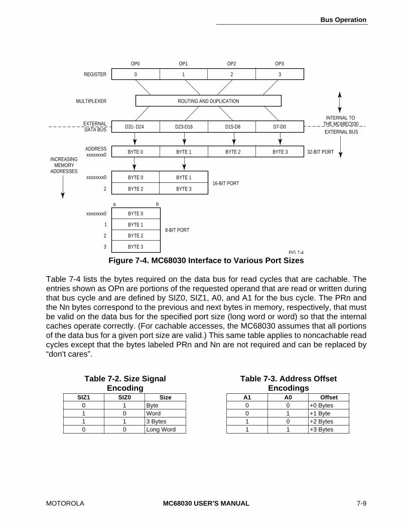
Bus Operation
MOTOROLA
MC68030 USER’S MANUAL
7-9
Table 7-4 lists the bytes required on the data bus for read cycles that are cachable. Theentries shown as OPn are portions of the requested operand that are read or written duringthat bus cycle and are defined by SIZ0, SIZ1, A0, and A1 for the bus cycle. The PRn andthe Nn bytes correspond to the previous and next bytes in memory, respectively, that mustbe valid on the data bus for the specified port size (long word or word) so that the internalcaches operate correctly. (For cachable accesses, the MC68030 assumes that all portionsof the data bus for a given port size are valid.) This same table applies to noncachable readcycles except that the bytes labeled PRn and Nn are not required and can be replaced by“don't cares”.
Figure 7-4. MC68030 Interface to Various Port Sizes
Table 7-2. Size Signal Encoding
Table 7-3. Address OffsetEncodings
SIZ1 SIZ0 Size A1 A0 Offset
0 1 Byte 0 0 +0 Bytes1 0 Word 0 1 +1 Byte1 1 3 Bytes 1 0 +2 Bytes0 0 Long Word 1 1 +3 Bytes
0 1 2 3
ROUTING AND DUPLICATION
BYTE 0
BYTE 2
BYTE 1
BYTE 316-BIT PORT
REGISTER
MULTIPLEXER
EXTERNALDATA BUS
ADDRESSxxxxxxxx0
xxxxxxxx0
2
INCREASINGMEMORY
ADDRESSES
D31- D24 D23-D16 D15-D8 D7-D0
BYTE 0 BYTE 1 BYTE 2 BYTE 3
BYTE 0
BYTE 1
BYTE 2
BYTE 3
8-BIT PORT2
3
1
xxxxxxxx0
EXTERNAL BUS
INTERNAL TOTHE MC68EC030
32-BIT PORT
OP0 OP1 OP2 OP3
FIG 7-4
a b
Bus Operation
7-10
MC68030 USER’S MANUAL
MOTOROLA
Table 7-4. Data Bus Requirements for Read Cycles.
Table 7-5 lists the combinations of SIZ0, SIZ1, A0, and A1 and the corresponding pattern ofthe data transfer for write cycles from the internal multiplexer of the MC68030 to the externaldata bus.
Figure 7-5 shows the transfer of a long-word operand to a word port. In the first bus cycle,the MC68030 places the four operand bytes on the external bus. Since the address is long-word aligned in this example, the multiplexer follows the pattern in the entry of Table 7-5corresponding to SIZ0_SIZ1_A0_A1=0000. The port latches the data on bits D16–D31 ofthe data bus, asserts DSACK1 (DSACK0 remains negated), and the processor terminatesthe bus cycle. It then starts a new bus cycle with SIZ0_SIZ1_A0_A1=1010 to transfer theremaining 16 bits. SIZ0 and SIZ1 indicate that a word remains to be transferred; A0 and A1indicate that the word corresponds to an offset of two from the base address. Themultiplexer follows the pattern corresponding to this configuration of the size and addresssignals and places the two least significant bytes of the long word on the word portion of thebus (D16–D31). The bus cycle transfers the remaining bytes to the word-size port. Figure 7-6 shows the timing of the bus transfer signals for this operation.
(Table did not make it over in the conversion from Word)

Bus Operation
MOTOROLA
MC68030 USER’S MANUAL
7-11
Table 7-5. MC68030 Internal to External Data Bus.
(Table did not make it over in the conversion from Word)
Figure 7-5. Example of Long-Word Transfer to Word Port
DATA BUSD31 D16
LONG WORD OPERAND
OP0 OP1 OP2 OP3
31 0
WORD MEMORY
MSB LSB
OP0 OP1
OP2 OP3
MC68EC030
SIZ1 SIZ0 A1 A00 0 0 0
1 0 1 0
MEMORY CONTROL
DSACK1 DSACK0L H
L H
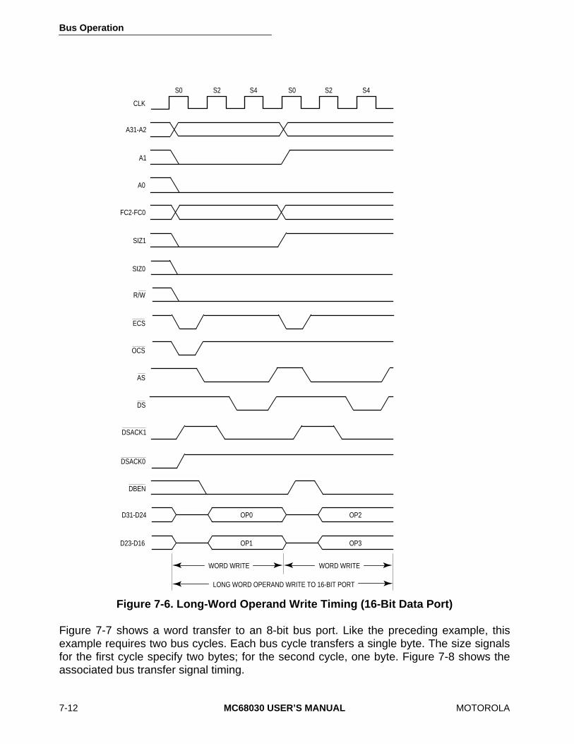
Bus Operation
7-12
MC68030 USER’S MANUAL
MOTOROLA
Figure 7-7 shows a word transfer to an 8-bit bus port. Like the preceding example, thisexample requires two bus cycles. Each bus cycle transfers a single byte. The size signalsfor the first cycle specify two bytes; for the second cycle, one byte. Figure 7-8 shows theassociated bus transfer signal timing.
Figure 7-6. Long-Word Operand Write Timing (16-Bit Data Port)
WORD WRITE
LONG WORD OPERAND WRITE TO 16-BIT PORT
S0 S2 S4 S0 S2 S4
CLK
A31-A2
A1
A0
FC2-FC0
SIZ1
SIZ0
R/W
ECS
OCS
AS
DS
DSACK1
DSACK0
DBEN
D31-D24
D23-D16
WORD WRITE
OP0
OP1
OP2
OP3

Bus Operation
MOTOROLA
MC68030 USER’S MANUAL
7-13
7.2.2 Misaligned Operands
Since operands may reside at any byte boundaries, they may be misaligned. A byteoperand is properly aligned at any address; a word operand is misaligned at an odd address;a long word is misaligned at an address that is not evenly divisible by four. The MC68000,MC68008, and MC68010 implementations allow long-word transfers on odd-wordboundaries but force exceptions if word or long-word operand transfers are attempted atodd-byte addresses. Although the MC68030 does not enforce any alignment restrictions fordata operands (including PC relative data addresses), some performance degradationoccurs when additional bus cycles are required for long-word or word operands that aremisaligned. For maximum performance, data items should be aligned on their naturalboundaries. All instruction words and extension words must reside on word boundaries.Attempting to prefetch an instruction word at an odd address causes an address errorexception.
Figure 7-7. Example of Word Transfer to Byte Port
DATA BUSD31 D24
WORD OPERAND
OP2 OP3
15 0
BYTE MEMORY
OP2
OP3
MC68EC030
SIZ1 SIZ0 A1 A01 0 0 0
0 1 0 1
MEMORY CONTROL
DSACK1 DSACK0LH
LH
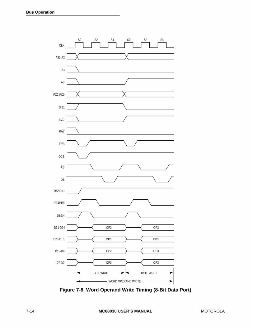
Bus Operation
7-14
MC68030 USER’S MANUAL
MOTOROLA
Figure 7-8. Word Operand Write Timing (8-Bit Data Port)
BYTE WRITE
WORD OPERAND WRITE
S0 S2 S4 S0 S2 S4
CLK
A31-A2
A1
A0
FC2-FC0
SIZ1
SIZ0
R/W
ECS
OCS
AS
DS
DSACK1
DSACK0
DBEN
D31-D24
D23-D16
BYTE WRITE
D15-D8
D7-D0 OP3
OP2
OP3
OP2
OP3
OP3
OP3
OP3
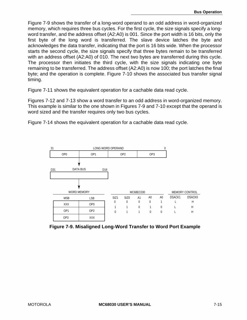
Bus Operation
MOTOROLA
MC68030 USER’S MANUAL
7-15
Figure 7-9 shows the transfer of a long-word operand to an odd address in word-organizedmemory, which requires three bus cycles. For the first cycle, the size signals specify a long-word transfer, and the address offset (A2:A0) is 001. Since the port width is 16 bits, only thefirst byte of the long word is transferred. The slave device latches the byte andacknowledges the data transfer, indicating that the port is 16 bits wide. When the processorstarts the second cycle, the size signals specify that three bytes remain to be transferredwith an address offset (A2:A0) of 010. The next two bytes are transferred during this cycle.The processor then initiates the third cycle, with the size signals indicating one byteremaining to be transferred. The address offset (A2:A0) is now 100; the port latches the finalbyte; and the operation is complete. Figure 7-10 shows the associated bus transfer signaltiming.
Figure 7-11 shows the equivalent operation for a cachable data read cycle.
Figures 7-12 and 7-13 show a word transfer to an odd address in word-organized memory.This example is similar to the one shown in Figures 7-9 and 7-10 except that the operand isword sized and the transfer requires only two bus cycles.
Figure 7-14 shows the equivalent operation for a cachable data read cycle.
Figure 7-9. Misaligned Long-Word Transfer to Word Port Example
DATA BUSD31 D16
LONG WORD OPERAND
OP0 OP1 OP2 OP3
31 0
WORD MEMORY
MSB LSB
XXX OP0
OP1 OP2
MC68EC030
SIZ1 SIZ0 A1 A00 0 0 0
1 1 0 1
MEMORY CONTROL
DSACK1 DSACK0L H
L H
XXXOP3
L H
A01
0
0 1 1 0 0
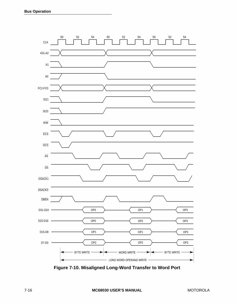
Bus Operation
7-16
MC68030 USER’S MANUAL
MOTOROLA
Figure 7-10. Misaligned Long-Word Transfer to Word Port
BYTE WRITE
LONG WORD OPERAND WRITE
S0 S2 S4 S0 S2 S4
CLK
A31-A2
A1
A0
FC2-FC0
SIZ1
SIZ0
R/W
ECS
OCS
AS
DS
DSACK1
DSACK0
DBEN
D31-D24
D23-D16
WORD WRITE
D15-D8
D7-D0
S0 S2 S4
OP0
OP0
OP1
OP2
OP1
OP2
OP1
OP2
OP3
OP3
OP3
OP3
BYTE WRITE
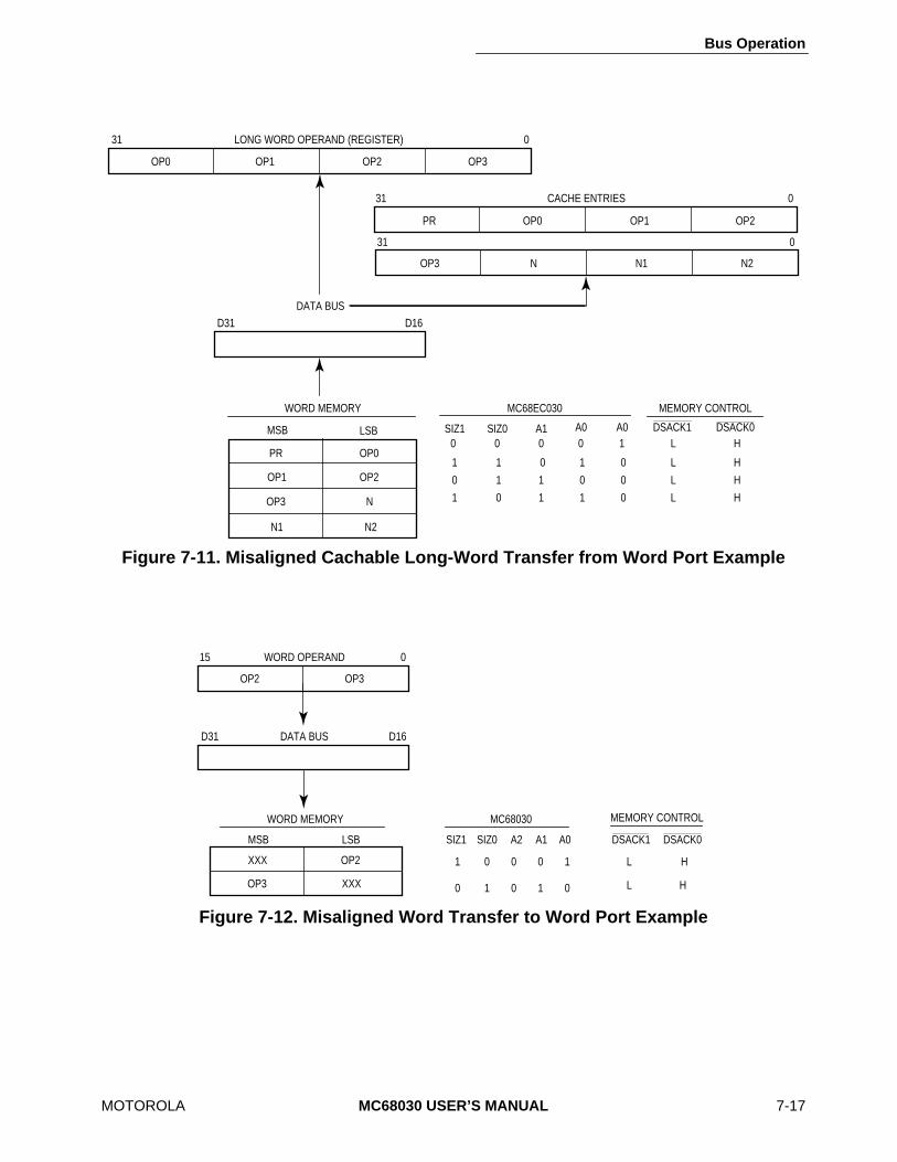
Bus Operation
MOTOROLA
MC68030 USER’S MANUAL
7-17
Figure 7-11. Misaligned Cachable Long-Word Transfer from Word Port Example
Figure 7-12. Misaligned Word Transfer to Word Port Example
LONG WORD OPERAND (REGISTER)
OP0 OP1 OP2 OP3
31 0
WORD MEMORY
MSB LSB
PR OP0
OP1 OP2
MC68EC030
SIZ1 SIZ0 A1 A00 0 0 0
1 1 0 1
MEMORY CONTROL
DSACK1 DSACK0L H
L H
NOP3
L H
A01
0
0 1 1 0 0
CACHE ENTRIES
PR OP0 OP1 OP2
31 0
OP3 N N1 N2
31 0
DATA BUS
D31 D16
N2N1
1 0 1 1 0 L H
MC68030
SIZ1 SIZ0 A2 A1
1 0 0 0 1
0 1 0 1 0
A0
MEMORY CONTROL
DSACK1 DSACK0
L H
L H
OP2 OP3
15 0WORD OPERAND
DATA BUSD31 D16
WORD MEMORY
MSB LSB
XXX
OP3
OP2
XXX
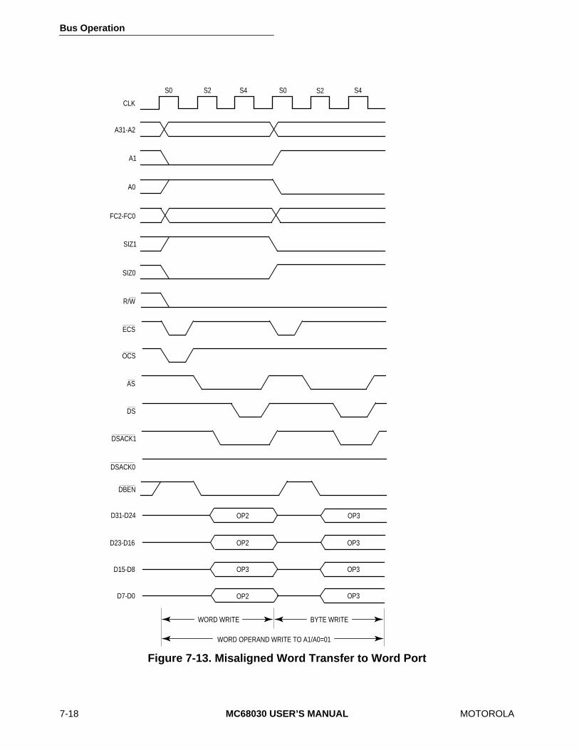
Bus Operation
7-18
MC68030 USER’S MANUAL
MOTOROLA
Figure 7-13. Misaligned Word Transfer to Word Port
WORD OPERAND WRITE TO A1/A0=01
S0 S2 S4 S0 S2 S4
CLK
A31-A2
A1
A0
FC2-FC0
SIZ1
SIZ0
R/W
ECS
OCS
AS
DS
DSACK1
DSACK0
DBEN
D31-D24
D23-D16
WORD WRITE
D15-D8
D7-D0
OP2
OP2
OP3
OP2
OP3
OP3
OP3
OP3
BYTE WRITE
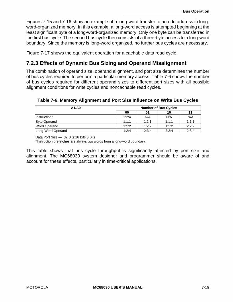
Bus Operation
MOTOROLA
MC68030 USER’S MANUAL
7-19
Figures 7-15 and 7-16 show an example of a long-word transfer to an odd address in long-word-organized memory. In this example, a long-word access is attempted beginning at theleast significant byte of a long-word-organized memory. Only one byte can be transferred inthe first bus cycle. The second bus cycle then consists of a three-byte access to a long-wordboundary. Since the memory is long-word organized, no further bus cycles are necessary.
Figure 7-17 shows the equivalent operation for a cachable data read cycle.
7.2.3 Effects of Dynamic Bus Sizing and Operand Misalignment
The combination of operand size, operand alignment, and port size determines the numberof bus cycles required to perform a particular memory access. Table 7-6 shows the numberof bus cycles required for different operand sizes to different port sizes with all possiblealignment conditions for write cycles and noncachable read cycles.
Data Port Size — 32 Bits:16 Bits:8 Bits*Instruction prefetches are always two words from a long-word boundary.
This table shows that bus cycle throughput is significantly affected by port size andalignment. The MC68030 system designer and programmer should be aware of andaccount for these effects, particularly in time-critical applications.
Table 7-6. Memory Alignment and Port Size Influence on Write Bus Cycles
A1/A0 Number of Bus Cycles00 01 10 11
Instruction* 1:2:4 N/A N/A N/AByte Operand 1:1:1 1:1:1 1:1:1 1:1:1Word Operand 1:1:2 1:2:2 1:1:2 2:2:2Long-Word Operand 1:2:4 2:3:4 2:2:4 2:3:4
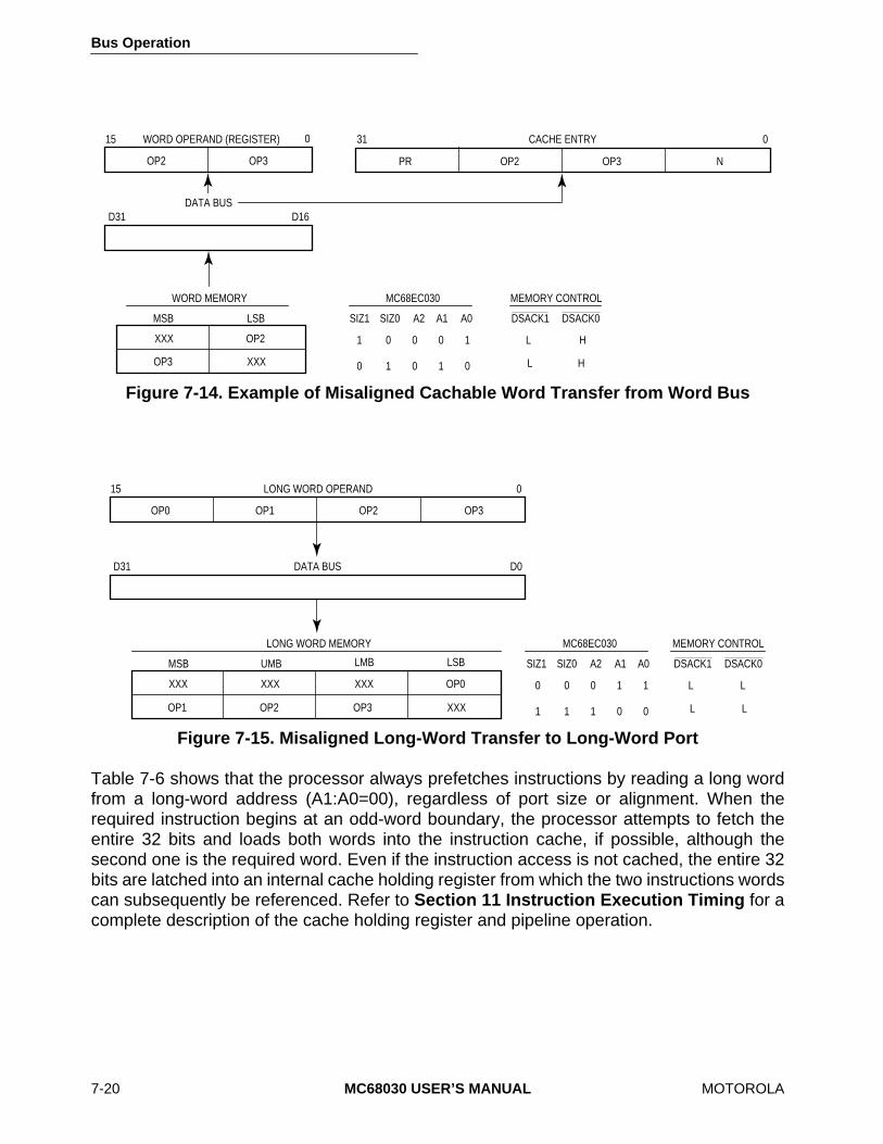
Bus Operation
7-20
MC68030 USER’S MANUAL
MOTOROLA
Table 7-6 shows that the processor always prefetches instructions by reading a long wordfrom a long-word address (A1:A0=00), regardless of port size or alignment. When therequired instruction begins at an odd-word boundary, the processor attempts to fetch theentire 32 bits and loads both words into the instruction cache, if possible, although thesecond one is the required word. Even if the instruction access is not cached, the entire 32bits are latched into an internal cache holding register from which the two instructions wordscan subsequently be referenced. Refer to
Section 11 Instruction Execution Timing
for acomplete description of the cache holding register and pipeline operation.
Figure 7-14. Example of Misaligned Cachable Word Transfer from Word Bus
Figure 7-15. Misaligned Long-Word Transfer to Long-Word Port
MC68EC030
SIZ1 SIZ0 A2 A1
1 0 0 0 1
0 1 0 1 0
A0
MEMORY CONTROL
DSACK1 DSACK0
L H
L H
OP2 OP3
15 0WORD OPERAND (REGISTER)
DATA BUSD31 D16
WORD MEMORY
MSB LSB
XXX
OP3
OP2
XXX
PR OP2
31 0CACHE ENTRY
OP3 N
MC68EC030
SIZ1 SIZ0 A2 A1
0 0 0 1 1
1 1 1 0 0
A0
MEMORY CONTROL
DSACK1 DSACK0
L
L L
OP0 OP1
15 0LONG WORD OPERAND
DATA BUSD31 D0
LONG WORD MEMORY
MSB UMB
XXX
OP1 OP2
XXX XXX
OP2 OP3
OP3
OP0
XXX
LMB LSB
L
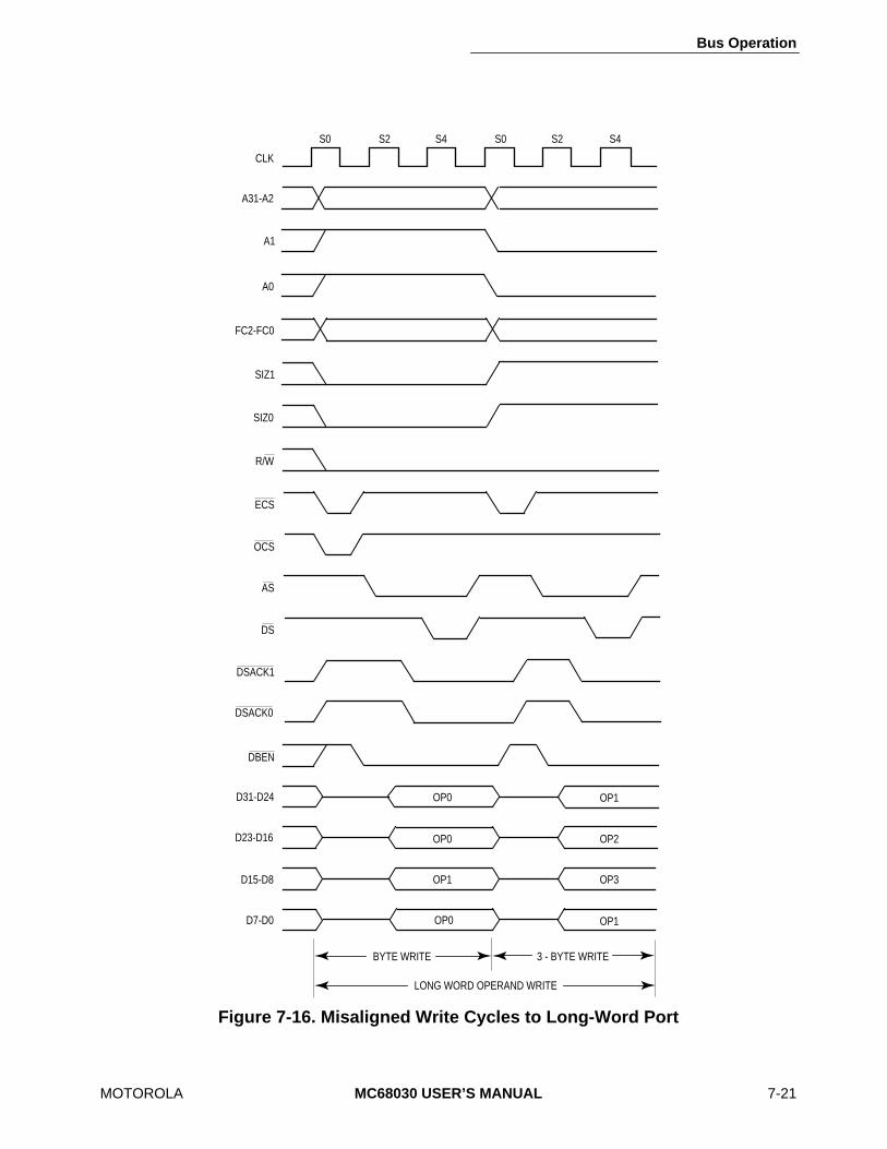
Bus Operation
MOTOROLA
MC68030 USER’S MANUAL
7-21
Figure 7-16. Misaligned Write Cycles to Long-Word Port
LONG WORD OPERAND WRITE
S0 S2 S4 S0 S2 S4
CLK
A31-A2
A1
A0
FC2-FC0
SIZ1
SIZ0
R/W
ECS
OCS
AS
DS
DSACK1
DSACK0
DBEN
D31-D24
D23-D16
BYTE WRITE
D15-D8
D7-D0
OP0
OP0
OP1
OP0
OP1
OP2
OP3
OP1
3 - BYTE WRITE
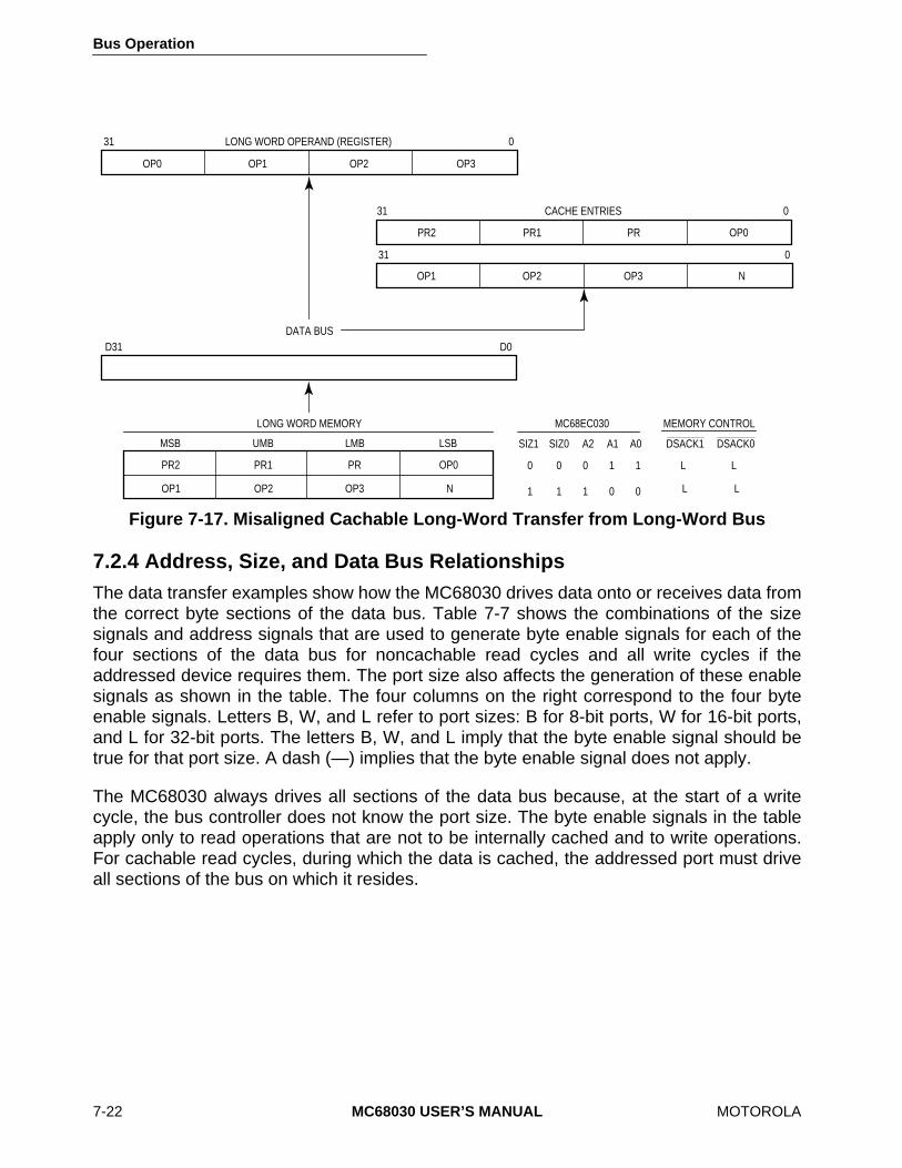
Bus Operation
7-22
MC68030 USER’S MANUAL
MOTOROLA
7.2.4 Address, Size, and Data Bus Relationships
The data transfer examples show how the MC68030 drives data onto or receives data fromthe correct byte sections of the data bus. Table 7-7 shows the combinations of the sizesignals and address signals that are used to generate byte enable signals for each of thefour sections of the data bus for noncachable read cycles and all write cycles if theaddressed device requires them. The port size also affects the generation of these enablesignals as shown in the table. The four columns on the right correspond to the four byteenable signals. Letters B, W, and L refer to port sizes: B for 8-bit ports, W for 16-bit ports,and L for 32-bit ports. The letters B, W, and L imply that the byte enable signal should betrue for that port size. A dash (—) implies that the byte enable signal does not apply.
The MC68030 always drives all sections of the data bus because, at the start of a writecycle, the bus controller does not know the port size. The byte enable signals in the tableapply only to read operations that are not to be internally cached and to write operations.For cachable read cycles, during which the data is cached, the addressed port must driveall sections of the bus on which it resides.
Figure 7-17. Misaligned Cachable Long-Word Transfer from Long-Word Bus
MC68EC030
SIZ1 SIZ0 A2 A1
0 0 0 1 1
1 1 1 0 0
A0
MEMORY CONTROL
DSACK1 DSACK0
L
L L
OP0 OP1
31 0LONG WORD OPERAND (REGISTER)
DATA BUSD31 D0
LONG WORD MEMORY
MSB UMB
PR2
OP1 OP2
PR1
OP2 OP3
PR
OP3
OP0
N
LMB LSB
L
PR2 PR1
31 0CACHE ENTRIES
PR OP0
OP1 OP2
31 0
OP3 N

Bus Operation
MOTOROLA MC68030 USER’S MANUAL 7-23
The table shows that the MC68030 transfers the number of bytes specified by the sizesignals to or from the specified address unless the operand is misaligned or the number ofbytes is greater than the port width. In these cases, the device transfers the greatest numberof bytes possible for the port. For example, if the size is four bytes and the address offset(A1:A0) is 01, a 32-bit slave can only receive three bytes in the current bus cycle. A 16- or8-bit[lz slave can only receive one byte. The table defines the byte enables for all port sizes.Byte data strobes can be obtained by combining the enable signals with the data strobesignal. Devices residing on 8-bit ports can use the data strobe by itself since there is onlyone valid byte for every transfer. These enable or strobe signals select only the bytesrequired for write cycles or for noncachable read cycles. The other bytes are not selected,which prevents incorrect accesses in sensitive areas such as I/O.
Figure 7-18 shows a logic diagram for one method for generating byte data enable signalsfor 16- and 32-bit ports from the size and address encodings and the read/write signal.
Table 7-7. Data Bus Write Enable Signals forByte, Word, and Long-Word Ports
Transfer Size
SIZ1 SIZ0 A1 A0Data Bus Active Sections
Byte (B) - Word (W) - Long-Word (L) PortsD31:D24 D23:D16 D15:D8 D7:D0
Byte 0000
1111
0011
0101
BWLBBWB
—WL—W
——L—
———L
Word 1111
0000
0011
0101
BWLBBWB
WLWLWW
—LL—
——LL
3 Byte 1111
1111
0011
0101
BWLBBWB
WLWLWW
LLL—
—LLL
Long Word 0000
0000
0011
0101
BWLBBWB
WLWLWW
LLL—
LLLL
Bus Operation
7-24 MC68030 USER’S MANUAL MOTOROLA
7.2.5 MC68030 versus MC68020 Dynamic Bus SizingThe MC68030 supports the dynamic bus sizing mechanism of the MC68020 forasynchronous bus cycles (terminated with DSACKx) with two restrictions. First, for acachable access within the boundaries of an aligned long word, the port size must beconsistent throughout the transfer of each long word. For example, when a byte port residesat address $00, addresses $01, $02, and $03 must also correspond to byte ports. Second,the port must supply as much data as it signals as port size, regardless of the transfer sizeindicated with the size signals and the address offset indicated by A0 and A1 for cachableaccesses. Otherwise, dynamic bus sizing is identical in the two processors.
7.2.6 Cache FillingThe on-chip data and instruction caches, described in Section 6 On-Chip CacheMemories, are each organized as 16 lines of four long-word entries each. For each line, atag contains the most significant bits of the logical address, FC2 (instruction cache) or FC0–FC2 (data cache), and a valid bit for each entry in the line. An entry fill operation loads anentire long word accessed from memory into a cache entry. This type of fill operation isperformed when one entry of a line is not valid and an access is cachable. A burst filloperation is requested when a tag miss occurs for the current cycle or when all four entiresin the cache line are invalid (provided the cache is enabled and burst filling for the cache isenabled). The burst fill operation attempts to fill all four entries in the line. To support burstfilling, the slave device must have a 32-bit port and must have a burst mode capability; thatis, it must acknowledge a burst request with the cache burst acknowledge (CBACK) signal.It must also terminate the burst accesses with STERM and place a long word on the databus for each transfer. The device may continue to supply successive long words, assertingSTERM with each one, until the cache line is full. For further information about filling thecache, both entry fills and burst mode fills, refer to 6.1.3 Cache Filling, 7.3.4 SynchronousRead Cycle, 7.3.5 Synchronous Write Cycle, and 7.3.7 Burst Operation Cycles, whichdiscuss in detail the required bus cycles.
Bus Operation
MOTOROLA MC68030 USER’S MANUAL 7-25
7.2.7 Cache InteractionsThe organization and requirements of the on-chip instruction and data caches affect theinterpretation of the DSACKx and STERM signals. Since the MC68030 attempts to load alldata operands and instructions that are cachable into the on-chip caches, the bus mayoperate differently when caching is enabled. Specifically, on cachable read cycles thatterminate normally, the low-order address signals (A0 and A1) and the size signals do notapply.
The slave device must supply as much aligned data on the data bus as its port size allows,regardless of the requested operand size. This means that an 8-bit port must supply a byte,a 16-bit port must supply a word, and a 32-bit port must supply an entire long word. Thisdata is loaded into the cache. For a 32-bit port, the slave device ignores A0 and A1 andsupplies the long word beginning at the long-word boundary on the data bus. For a 16-bit[lzport, the device ignores A0 and supplies the entire word beginning at the lower wordboundary on D16–D31 of the data bus. For a byte port, the device supplies the addressedbyte on D24–D31.
If the addressed device cannot supply port-sized data or if the data should not be cached,the device must assert cache inhibit in (CIIN) as it terminates the read cycle. If the bus cycleterminates abnormally, the MC68030 does not cache the data. For details of interactions ofport sizes, misalignments, and cache filling, refer to 6.1.3 Cache Filling.
The caches can also affect the assertion of AS and the operation of a read cycle. The searchof the appropriate cache by the processor begins when the microsequencer requires aninstruction or a data item. At this time, the bus controller may also initiate an external buscycle in case the requested item is not resident in the instruction or data cache. If the bus isnot occupied with another read or write cycle, the bus controller asserts the ECS signal (andthe OCS signal, if appropriate). If an internal cache hit occurs, the external cycle aborts, andAS is not asserted. This makes it possible to have ECS asserted on multiple consecutiveclock cycles. Notice that there is a minimum time specified from the negation of ECS to thenext assertion of ECS (refer to MC68030EC/D, MC68030 Electrical Specifications.
Instruction prefetches can occur every other clock so that if, after an aborted cycle due to aninstruction cache hit, the bus controller asserts ECS on the next clock, this second cycle isfor a data fetch. However, data accesses that hit in the data cache can also cause theassertion of ECS and an aborted cycle. Therefore, since instruction and data accesses aremixed, it is possible to see multiple successive ECS assertions on the external bus if theprocessor is hitting in both caches and if the bus controller is free. Note that, if the buscontroller is executing other cycles, these aborted cycles due to cache hits may not be seenexternally. Also, OCS is asserted for the first external cycle of an operand transfer.Therefore, in the case of a misaligned data transfer where the first portion of the operandresults in a cache hit (but the bus controller did not begin an external cycle and then abortit) and the second portion in a cache miss, OCS is asserted for the second portion of theoperand.

Bus Operation
7-26 MC68030 USER’S MANUAL MOTOROLA
Figure 7-18. Byte Data Select Generation for 16- and 32-Bit Ports
A1
SIZ0
SIZ1
R/W
LD
UD
LLD
LMD
UMD
UUD
UUD = UPPER UPPER DATA (32-BIT PORT)UMD = UPPER MIDDLE DATA (32-BIT PORT)LMD = LOWER MIDDLE DATA (32-BIT PORT)LLD = LOWER LOWER DATA (32-BIT PORT)UD = UPPER DATA (16-BIT PORT)LD = LOWER DATA (16-BIT PORT)
NOTE: These select lines can be combined with the address decode circuitry or all can be generated within the same programmed array logic unit.
A0

Bus Operation
MOTOROLA MC68030 USER’S MANUAL 7-27
7.2.8 Asynchronous OperationThe MC68030 bus may be used in an asynchonous manner. In that case, the externaldevices connected to the bus can operate at clock frequencies different from the clock forthe MC68030. Asynchronous operation requires using only the handshake line (AS, DS,DSACK1, DSACK0, BERR, and HALT) to control data transfers. Using this method, ASsignals the start of a bus cycle, and DS is used as a condition for valid data on a write cycle.Decoding the size outputs and lower address lines (A0 and A1) provides strobes that selectthe active portion of the data bus. The slave device (memory or peripheral) then respondsby placing the requested data on the correct portion of the data bus for a read cycle orlatching the data on a write cycle, and asserting the DSACK1/DSACK0 combination thatcorresponds to the port size to terminate the cycle. If no slave responds or the access isinvalid, external control logic asserts the BERR or BERR and HALT signal(s) to abort or retrythe bus cycle, respectively.
The DSACKx signals can be asserted before the data from a slave device is valid on a readcycle. The length of time that DSACKx may precede data is given by parameter #31, and itmust be met in any asynchronous system to insure that valid data is latched into theprocessor. (Refer to MC68030EC/D, MC68030 Electrical Specifications for timingparameters.) Notice that no maximum time is specified from the assertion of AS to theassertion of DSACKx. Although the processor can transfer data in a minimum of three clockcycles when the cycle is terminated with DSACKx, the processor inserts wait cycles in clockperiod increments until DSACKx is recognized.
The BERR and/or HALT signals can be asserted after the DSACKx signal(s) is asserted.BERR and/or HALT must be asserted within the time given as parameter #48, after DSACKxis asserted in any asynchronous system. If this maximum delay time is violated, theprocessor may exhibit erratic behavior.
Bus Operation
7-28 MC68030 USER’S MANUAL MOTOROLA
For asynchronous read cycles, the value of CIIN is internally latched on the rising edge ofbus cycle state 4. Refer to 7.3.1 Asynchronous Read Cycle for more details on the statesfor asynchonous read cycles.
During any bus cycle terminated by DSACKx or BERR, the assertion of CBACK iscompletely ignored.
7.2.9 Synchronous Operation with DSACKxAlthough cycles terminated with the DSACKx signals are classified as asynchronous andcycles terminated with STERM are classified as synchronous, cycles terminated withDSACKx can also operate synchronously in that signals are interpreted relative to clockedges.
The devices that use these cycles must synchronize the responses to the MC68030 clockto be synchronous. Since they terminate bus cycles with the DSACKx signals, the dynamicbus sizing capabilities of the MC68030 are available. In addition, the minimum cycle time forthese cycles is also three clocks.
To support those systems that use the system clock to generate DSACKx and otherasynchronous inputs, the asynchronous input setup time (parameter #47A) and theasynchronous input hold time (parameter #47B) are given. If the setup and hold times aremet for the assertion or negation of a signal, such as DSACKx, the processor can beguaranteed to recognize that signal level on that specific falling edge of the system clock. Ifthe assertion of DSACKx is recognized on a particular falling edge of the clock, valid data islatched into the processor (for a read cycle) on the next falling clock edge provided the datameets the data setup time (parameter #27). In this case, parameter #31 for asynchronousoperation can be ignored. The timing parameters referred to are described in MC68030EC/D, MC68030 Electrical Specifications. If a system asserts DSACKx for the required windowaround the falling edge of S2 and obeys the proper bus protocol by maintaining DSACKx(and/or BERR/HALT) until and throughout the clock edge that negates AS (with theappropriate asynchronous input hold time specified by parameter #47B), no wait states areinserted. The bus cycle runs at its maximum speed (three clocks per cycle) for bus cyclesterminated with DSACKx.
Bus Operation
MOTOROLA MC68030 USER’S MANUAL 7-29
To assure proper operation in a synchronous system when BERR or BERR and HALT isasserted after DSACKx, BERR (and HALT) must meet the appropriate setup time(parameter #27A) prior to the falling clock edge one clock cycle after DSACKx is recognized.This setup time is critical, and the MC68030 may exhibit erratic behavior if it is violated.
When operating synchronously, the data-in setup and hold times for synchronous cyclesmay be used instead of the timing requirements for data relative to the DS signal.
The value of CIIN is latched on the rising edge of bus cycle state 4 for all cycles terminatedwith DSACKx.
7.2.10 Synchronous Operation with STERMThe MC68030 supports synchronous bus cycles terminated with STERM. These cycles, for32-bit ports only, are similar to cycles terminated with DSACKx. The main difference is thatSTERM can be asserted (and data can be transferred) earlier than for a cycle terminatedwith DSACKx, causing the processor to perform a minimum access time transfer in twoclock periods. However, wait cycles can be inserted by delaying the assertion of STERMappropriately.
Using STERM instead of DSACKx in any bus cycle makes the cycle synchronous. Any buscycle is synchronous if:
1. Neither DSACKx nor AVEC is recognized during the cycle.
2. The port size is 32 bits.
3. Synchronous input setup and hold time requirements (specifications #60 and #61) for STERM are met.
Burst mode operation requires the use of STERM to terminate each of its cycles. The firstcycle of any burst transfer must be a synchronous cycle as described in the precedingparagraph. The exact timing of this cycle is controlled by the assertion of STERM, and waitcycles can be inserted as necessary. However, the minimum cycle time is two clocks. If aburst operation is initiated and allowed to terminate normally, the second, third, and fourthcycles latch data on successive falling edges of the clock at a minimum. Again, the exacttiming for these subsequent cycles is controlled by the timing of STERM for each of thesecycles, and wait cycles can be inserted as necessary.
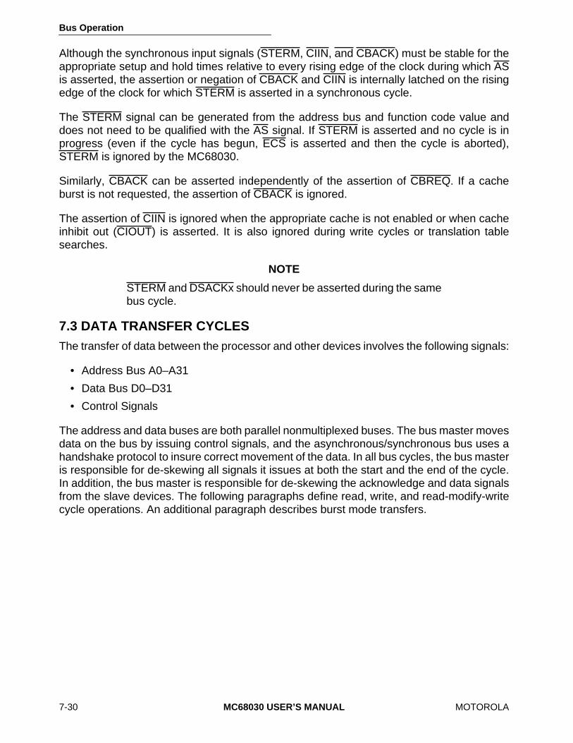
Bus Operation
7-30 MC68030 USER’S MANUAL MOTOROLA
Although the synchronous input signals (STERM, CIIN, and CBACK) must be stable for theappropriate setup and hold times relative to every rising edge of the clock during which ASis asserted, the assertion or negation of CBACK and CIIN is internally latched on the risingedge of the clock for which STERM is asserted in a synchronous cycle.
The STERM signal can be generated from the address bus and function code value anddoes not need to be qualified with the AS signal. If STERM is asserted and no cycle is inprogress (even if the cycle has begun, ECS is asserted and then the cycle is aborted),STERM is ignored by the MC68030.
Similarly, CBACK can be asserted independently of the assertion of CBREQ. If a cacheburst is not requested, the assertion of CBACK is ignored.
The assertion of CIIN is ignored when the appropriate cache is not enabled or when cacheinhibit out (CIOUT) is asserted. It is also ignored during write cycles or translation tablesearches.
NOTE
STERM and DSACKx should never be asserted during the samebus cycle.
7.3 DATA TRANSFER CYCLESThe transfer of data between the processor and other devices involves the following signals:
• Address Bus A0–A31
• Data Bus D0–D31
• Control Signals
The address and data buses are both parallel nonmultiplexed buses. The bus master movesdata on the bus by issuing control signals, and the asynchronous/synchronous bus uses ahandshake protocol to insure correct movement of the data. In all bus cycles, the bus masteris responsible for de-skewing all signals it issues at both the start and the end of the cycle.In addition, the bus master is responsible for de-skewing the acknowledge and data signalsfrom the slave devices. The following paragraphs define read, write, and read-modify-writecycle operations. An additional paragraph describes burst mode transfers.

Bus Operation
MOTOROLA MC68030 USER’S MANUAL 7-31
Each of the bus cycles is defined as a succession of states. These states apply to the busoperation and are different from the processor states described in Section 4 ProcessingStates. The clock cycles used in the descriptions and timing diagrams of data transfercycles are independent of the clock frequency. Bus operations are described in terms ofexternal bus states.
7.3.1 Asynchronous Read CycleDuring a read cycle, the processor receives data from a memory, coprocessor, or peripheraldevice. If the instruction specifies a long-word operation, the MC68030 attempts to read fourbytes at once. For a word operation, it attempts to read two bytes at once, and for a byteoperation, one byte. For some operations, the processor requests a three-byte transfer. Theprocessor properly positions each byte internally. The section of the data bus from whicheach byte is read depends on the operand size, address signals (A0–A1), CIIN and CIOUT,whether the internal caches are enabled, and the port size. Refer to 7.2.1 Dynamic BusSizing, 7.2.2 Misaligned Operands, and 7.2.6 Cache Filling for more information ondynamic bus sizing, misaligned operands, and cache interactions.
Figure 7-19 is a flowchart of an asynchronous long-word read cycle. Figure 7-20 is aflowchart of a byte read cycle. The following figures show functional read cycle timingdiagrams specified in terms of clock periods. Figure 7-21 corresponds to byte and word readcycles from a 32-bit port. Figure 7-22 corresponds to a long-word read cycle from an 8-bitport. Figure 7-23 also applies to a long-word read cycle, but from a 16-bit port.
State 0The read cycle starts in state 0 (S0). The processor drives ECS low, indicating thebeginning of an external cycle. When the cycle is the first external cycle of a read operandoperation, operand cycle start (OCS) is driven low at the same time. During S0, theprocessor places a valid address on A0–A31 and valid function codes on FC0–FC2. Thefunction codes select the address space for the cycle. The processor drives R/W high fora read cycle and drives DBEN inactive to disable the data buffers. SIZ0–SIZ1 becomevalid, indicating the number of bytes requested to be transferred. CIOUT also becomesvalid, indicating the state of the MMU CI bit in the address translation descriptor or in theappropriate TTx register.
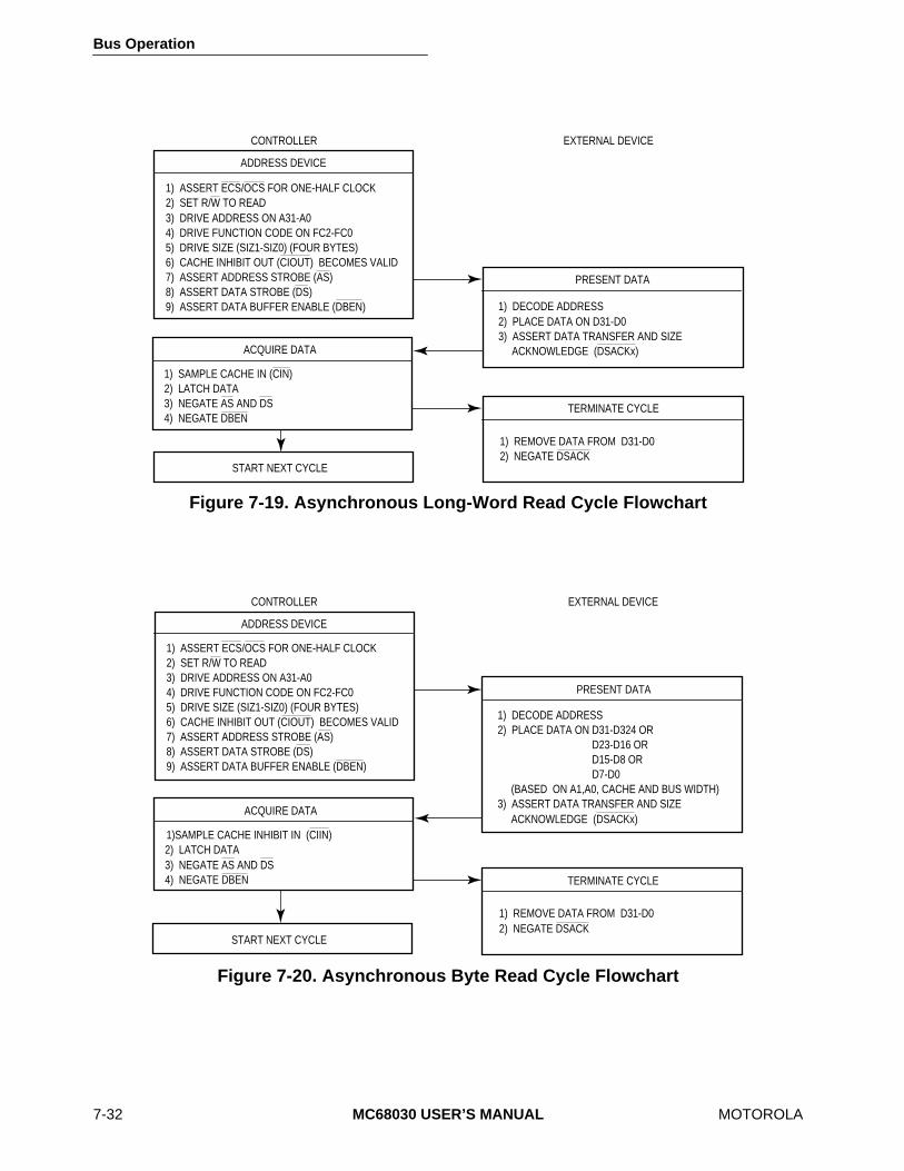
Bus Operation
7-32 MC68030 USER’S MANUAL MOTOROLA
Figure 7-19. Asynchronous Long-Word Read Cycle Flowchart
Figure 7-20. Asynchronous Byte Read Cycle Flowchart
CONTROLLER
ADDRESS DEVICE
1) ASSERT ECS/OCS FOR ONE-HALF CLOCK2) SET R/W TO READ3) DRIVE ADDRESS ON A31-A04) DRIVE FUNCTION CODE ON FC2-FC05) DRIVE SIZE (SIZ1-SIZ0) (FOUR BYTES)6) CACHE INHIBIT OUT (CIOUT) BECOMES VALID7) ASSERT ADDRESS STROBE (AS)8) ASSERT DATA STROBE (DS)9) ASSERT DATA BUFFER ENABLE (DBEN)
ACQUIRE DATA
2) LATCH DATA3) NEGATE AS AND DS4) NEGATE DBEN
START NEXT CYCLE
PRESENT DATA
1) DECODE ADDRESS2) PLACE DATA ON D31-D03) ASSERT DATA TRANSFER AND SIZE ACKNOWLEDGE (DSACKx)
TERMINATE CYCLE
1) REMOVE DATA FROM D31-D02) NEGATE DSACK
EXTERNAL DEVICE
1) SAMPLE CACHE IN (CIN)
START NEXT CYCLE
PRESENT DATA
1) DECODE ADDRESS2) PLACE DATA ON D31-D324 OR D23-D16 OR D15-D8 OR D7-D0 (BASED ON A1,A0, CACHE AND BUS WIDTH)3) ASSERT DATA TRANSFER AND SIZE ACKNOWLEDGE (DSACKx)
TERMINATE CYCLE
1) REMOVE DATA FROM D31-D02) NEGATE DSACK
EXTERNAL DEVICECONTROLLER
ADDRESS DEVICE
1) ASSERT ECS/OCS FOR ONE-HALF CLOCK2) SET R/W TO READ3) DRIVE ADDRESS ON A31-A04) DRIVE FUNCTION CODE ON FC2-FC05) DRIVE SIZE (SIZ1-SIZ0) (FOUR BYTES)6) CACHE INHIBIT OUT (CIOUT) BECOMES VALID7) ASSERT ADDRESS STROBE (AS)8) ASSERT DATA STROBE (DS)9) ASSERT DATA BUFFER ENABLE (DBEN)
ACQUIRE DATA
2) LATCH DATA3) NEGATE AS AND DS4) NEGATE DBEN
1)SAMPLE CACHE INHIBIT IN (CIIN)
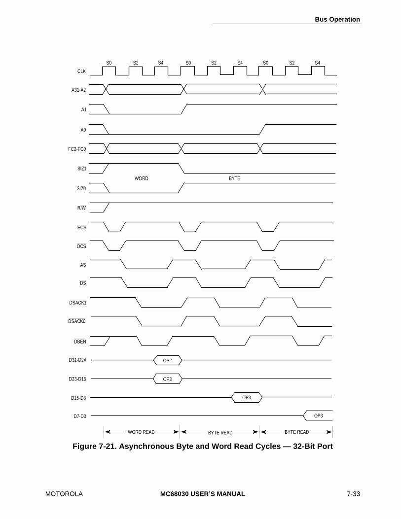
Bus Operation
MOTOROLA MC68030 USER’S MANUAL 7-33
Figure 7-21. Asynchronous Byte and Word Read Cycles — 32-Bit Port
WORD READ
S0 S2 S4 S0 S2 S4
BYTE READ
CLK
A31-A2
A1
A0
FC2-FC0
SIZ1
SIZ0
R/W
ECS
OCS
AS
DS
DSACK1
DSACK0
DBEN
D31-D24
D23-D16
D15-D8
D7-D0
S0 S2 S4
OP2
OP3
OP3
OP3
BYTEWORD
BYTE READ
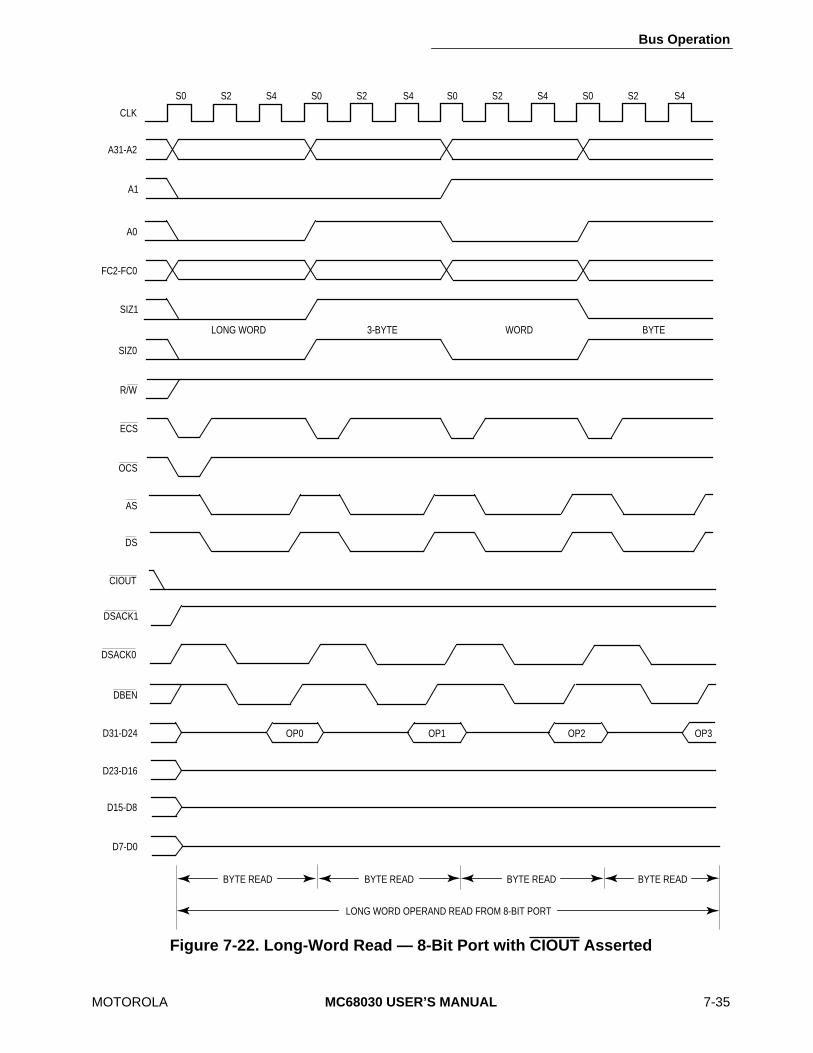
Bus Operation
MOTOROLA MC68030 USER’S MANUAL 7-35
Figure 7-22. Long-Word Read — 8-Bit Port with CIOUT Asserted
CLK
A31-A2
A1
A0
FC2-FC0
SIZ1
SIZ0
R/W
ECS
OCS
AS
DS
DSACK1
CIOUT
DSACK0
DBEN
D31-D24
D23-D16
D15-D8
D7-D0
BYTE READ
OP0 OP1 OP3
LONG WORD 3-BYTE
BYTE READ
WORD BYTE
OP2
BYTE READBYTE READ
LONG WORD OPERAND READ FROM 8-BIT PORT
S0 S2 S4 S0 S2 S4 S0 S2 S4 S0 S2 S4
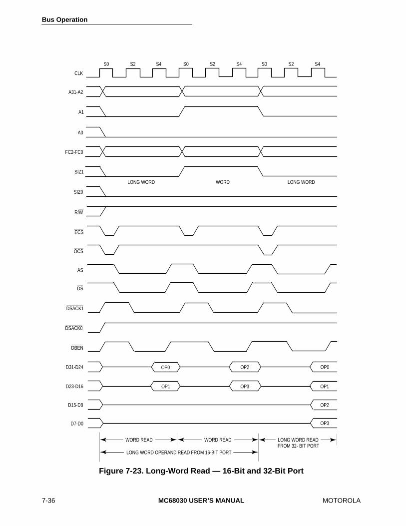
Bus Operation
7-36 MC68030 USER’S MANUAL MOTOROLA
Figure 7-23. Long-Word Read — 16-Bit and 32-Bit Port
CLK
A31-A2
A1
A0
FC2-FC0
SIZ1
SIZ0
R/W
ECS
OCS
AS
DS
DSACK1
DSACK0
DBEN
D31-D24
D23-D16
D15-D8
D7-D0
WORD READ
S0 S2 S4 S0 S2 S4
WORD READ
S0 S2 S4
OP0
OP1 OP3
OP3
LONG WORD WORD
LONG WORD READFROM 32- BIT PORT
OP2
OP1
OP0OP2
LONG WORD
LONG WORD OPERAND READ FROM 16-BIT PORT

Bus Operation
MOTOROLA MC68030 USER’S MANUAL 7-37
State 1One-half clock later in state 1 (S1), the processor asserts AS indicating that the addresson the address bus is valid. The processor also asserts DS also during S1. In addition,the ECS (and OCS, if asserted) signal is negated during S1.
State 2During state 2 (S2), the processor asserts DBEN to enable external data buffers. Theselected device uses R/W, SIZ0–SIZ1, A0–A1, CIOUT, and DS to place its information onthe data bus, and drives CIIN if appropriate. Any or all of the bytes (D24–D31, D16–D23,D8–D15, and D0–D7) are selected by SIZ0–SIZ1 and A0–A1. Concurrently, the selecteddevice asserts DSACKx.
State 3As long as at least one of the DSACKx signals is recognized by the end of S2 (meetingthe asynchronous input setup time requirement), data is latched on the next falling edgeof the clock, and the cycle terminates. If DSACKx is not recognized by the start of state 3(S3), the processor inserts wait states instead of proceeding to states 4 and 5. To ensurethat wait states are inserted, both DSACK0 and DSACK1 must remain negatedthroughout the asynchronous input setup and hold times around the end of S2. If waitstates are added, the processor continues to sample the DSACKx signals on the fallingedges of the clock until one is recognized.
State 4The processor samples CIIN at the beginning of state 4 (S4). Since CIIN is defined as asynchronous input, whether asserted or negated, it must meet the appropriatesynchronous input setup and hold times on every rising edge of the clock while AS isasserted. At the end of S4, the processor latches the incoming data.
State 5The processor negates AS, DS, and DBEN during state 5 (S5). It holds the address validduring S5 to provide address hold time for memory systems. R/W, SIZ0–SIZ1, and FC0–FC2 also remain valid throughout S5.
The external device keeps its data and DSACKx signals asserted until it detects thenegation of AS or DS (whichever it detects first). The device must remove its data andnegate DSACKx within approximately one clock period after sensing the negation of ASor DS. DSACKx signals that remain asserted beyond this limit may be prematurelydetected for the next bus cycle.

Bus Operation
7-38 MC68030 USER’S MANUAL MOTOROLA
7.3.2 Asynchronous Write CycleDuring a write cycle, the processor transfers data to memory or a peripheral device.
Figure 7-24 is a flowchart of a write cycle operation for a long-word transfer. The followingfigures show the functional write cycle timing diagrams specified in terms of clock periods.Figure 7-25 shows two write cycles (between two read cycles with no idle time) for a 32-bitport. Figure 7-26 shows byte and word write cycles to a 32-bit port. Figure 7-27 shows along-word write cycle to an 8-bit port. Figure 7-28 shows a long-word write cycle to a 16-bitport.
Figure 7-24. Asynchronous Write Cycle Flowchart
1) ASSERT ECS/OCS FOR ONE-HALF CLOCK2) DRIVE ADDRESS ON A31-A03) DRIVE FUNCTION CODE ON FC2-FC04) DRIVE SIZE (SIZ1-SIZ0) (FOUR BYTES)5) SET R/W TO WRITE6) CACHE INHIBIT OUT (CIOUT) BECOMES VALID7) ASSERT ADDRESS STROBE (AS)8) ASSERT DATA BUFFER ENABLE (DBEN)9) DRIVE DATA LINES D31-D0
10) ASSERT DATA STROBE (DS)
1) NEGATE AS AND DS2) REMOVE DATA FROM D31-D03) NEGATE DBEN
EXTERNAL DEVICECONTROLLER
1) NEGATE DSACKx
TERMINATE CYCLE
ACCEPT DATA
1) DECODE ADDRSS2) STORE DATA FROM D31-D03) ASSERT DATA TRANSFER AND SIZE ACKNOWLEDGE (DSACKx)
ADDRESS DEVICE
TERMINATE OUTPUT TRANSFER
START NEXT CYCLE

Bus Operation
MOTOROLA MC68030 USER’S MANUAL 7-39
State 0The write cycle starts in S0. The processor drives ECS low, indicating the beginning ofan external cycle. When the cycle is the first external cycle of a write operation, OCS isdriven low at the same time. During S0, the processor places a valid address on A0–A31and valid function codes on FC0–FC2. The function codes select the address space forthe cycle. The processor drives R/W low for a write cycle. SIZ0–SIZ1 become valid,indicating the number of bytes to be transferred. CIOUT also becomes valid, indicating
Figure 7-25. Asynchronous Read-Write-Read Cycles — 32-Bit Port
CLK
A31-A2
A1
A0
FC2-FC0
SIZ1
SIZ0
R/W
ECS
OCS
AS
DS
DSACK1
DSACK0
DBEN
D31-D0
WRITE
LONG WORD
WRITE READ
S0 S2 S4 S0 S2 S4 S0 S2 S4 S0 S2 Sw Sw S4
READ WITH WAIT STATES

Bus Operation
7-40 MC68030 USER’S MANUAL MOTOROLA
the state of the MMU CI bit in the address translation descriptor or in the appropriate TTxregister.
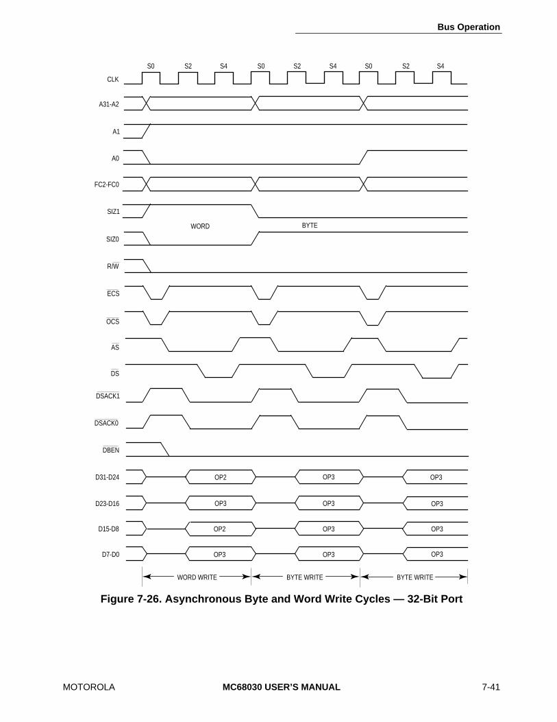
Bus Operation
MOTOROLA MC68030 USER’S MANUAL 7-41
Figure 7-26. Asynchronous Byte and Word Write Cycles — 32-Bit Port
CLK
A31-A2
A1
A0
FC2-FC0
SIZ1
SIZ0
R/W
ECS
OCS
AS
DS
DSACK1
DSACK0
DBEN
D31-D24
D23-D16
D15-D8
D7-D0
WORD WRITE
S0 S2 S4 S0 S4
BYTE WRITE
S0 S2S2 S4
OP2
OP3 OP3
OP3
WORD
OP3
OP3
OP3OP3
BYTE
OP2
OP3 OP3
OP3
BYTE WRITE
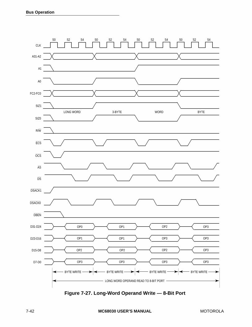
Bus Operation
7-42 MC68030 USER’S MANUAL MOTOROLA
Figure 7-27. Long-Word Operand Write — 8-Bit Port
CLK
A31-A2
A1
A0
FC2-FC0
SIZ1
SIZ0
R/W
ECS
OCS
AS
DS
DSACK1
DSACK0
DBEN
D31-D24
D23-D16
D15-D8
D7-D0
BYTE WRITE
LONG WORD 3-BYTE
BYTE WRITE
WORD BYTE
BYTE WRITEBYTE WRITE
LONG WORD OPERAND READ TO 8-BIT PORT
S0 S2 S2S4 S0 S4 S0 S2 S4 S0 S2 S4
OP0 OP3OP2OP1
OP1 OP3OP3OP1
OP2 OP3OP2OP2
OP3 OP3OP3OP3
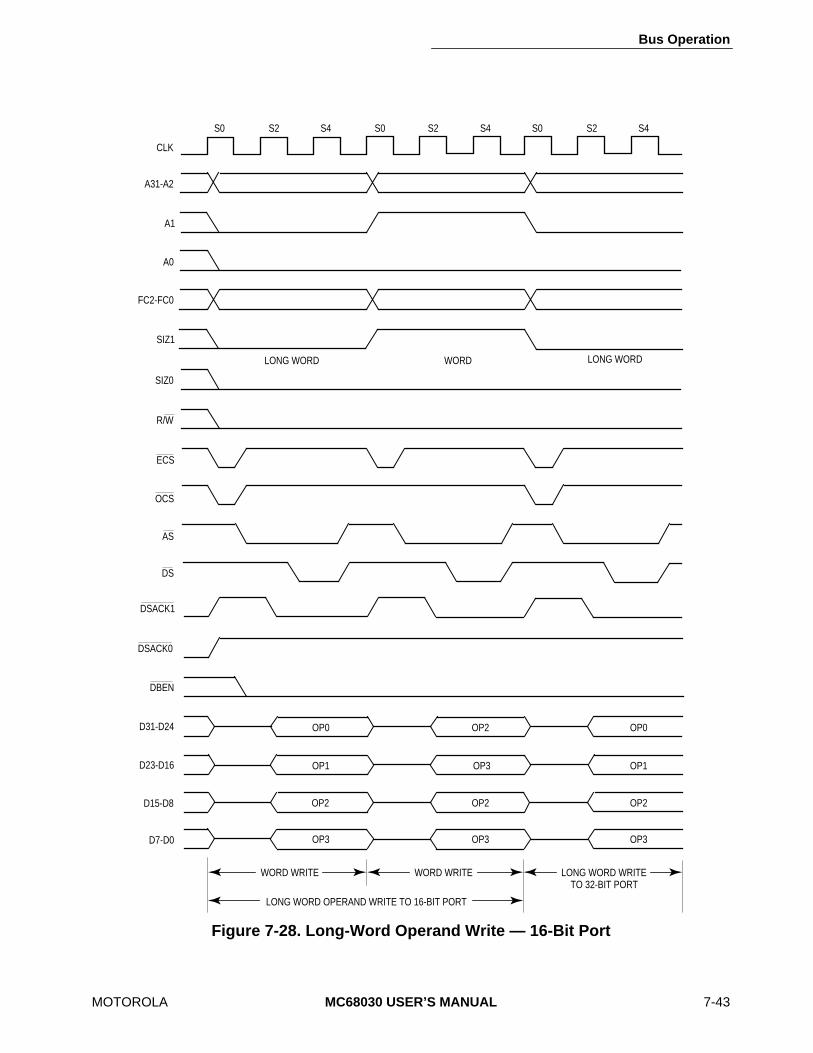
Bus Operation
MOTOROLA MC68030 USER’S MANUAL 7-43
Figure 7-28. Long-Word Operand Write — 16-Bit Port
CLK
A31-A2
A1
A0
FC2-FC0
SIZ1
SIZ0
R/W
ECS
OCS
AS
DS
DSACK1
DSACK0
DBEN
D31-D24
D23-D16
D15-D8
D7-D0
WORD WRITE
S0 S2 S2S4 S0 S4
WORD WRITE
S0 S2 S4
OP0
OP1 OP3
OP3
LONG WORD
OP2
OP1
OP0OP2
WORD
OP2
OP3 OP3
OP2
LONG WORD WRITETO 32-BIT PORT
LONG WORD OPERAND WRITE TO 16-BIT PORT
LONG WORD
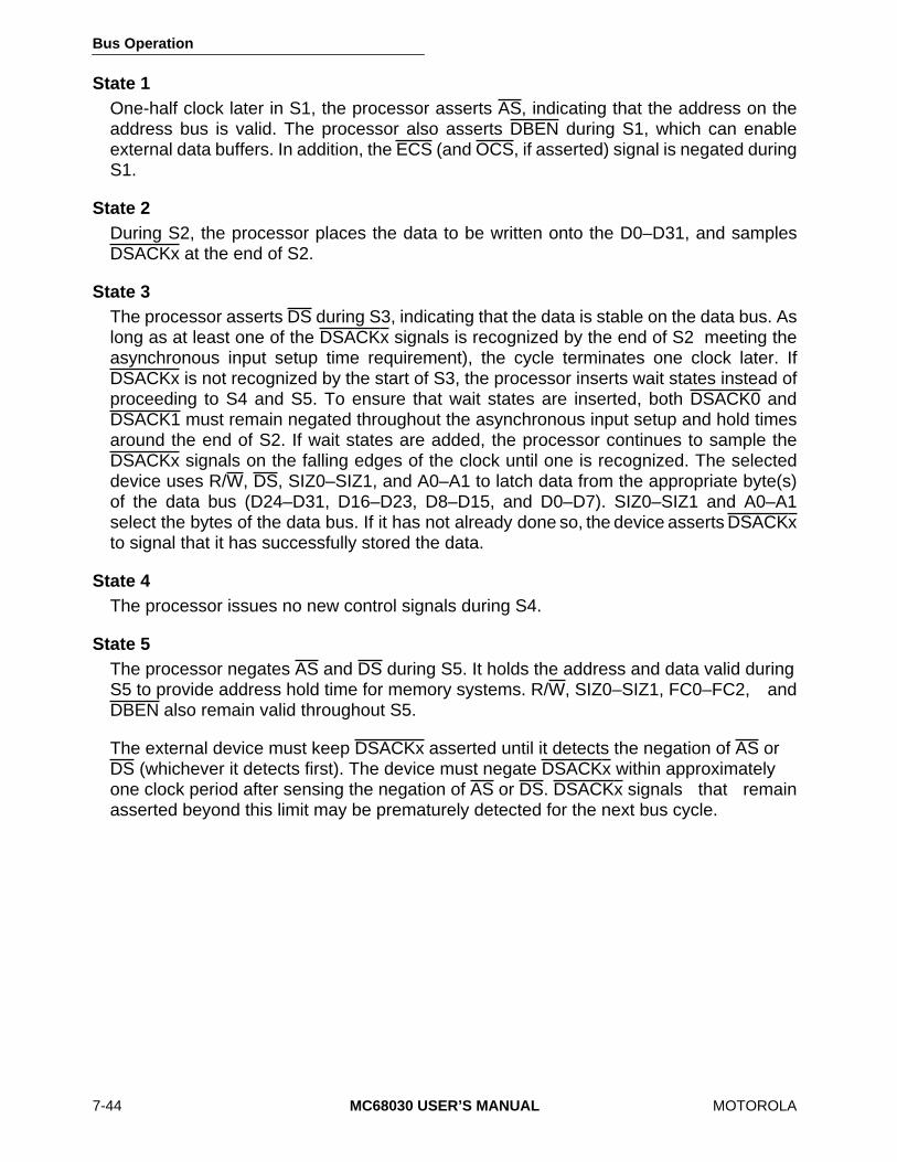
Bus Operation
7-44 MC68030 USER’S MANUAL MOTOROLA
State 1One-half clock later in S1, the processor asserts AS, indicating that the address on theaddress bus is valid. The processor also asserts DBEN during S1, which can enableexternal data buffers. In addition, the ECS (and OCS, if asserted) signal is negated duringS1.
State 2During S2, the processor places the data to be written onto the D0–D31, and samplesDSACKx at the end of S2.
State 3The processor asserts DS during S3, indicating that the data is stable on the data bus. Aslong as at least one of the DSACKx signals is recognized by the end of S2 meeting theasynchronous input setup time requirement), the cycle terminates one clock later. IfDSACKx is not recognized by the start of S3, the processor inserts wait states instead ofproceeding to S4 and S5. To ensure that wait states are inserted, both DSACK0 andDSACK1 must remain negated throughout the asynchronous input setup and hold timesaround the end of S2. If wait states are added, the processor continues to sample theDSACKx signals on the falling edges of the clock until one is recognized. The selecteddevice uses R/W, DS, SIZ0–SIZ1, and A0–A1 to latch data from the appropriate byte(s)of the data bus (D24–D31, D16–D23, D8–D15, and D0–D7). SIZ0–SIZ1 and A0–A1select the bytes of the data bus. If it has not already done so, the device asserts DSACKxto signal that it has successfully stored the data.
State 4The processor issues no new control signals during S4.
State 5The processor negates AS and DS during S5. It holds the address and data valid duringS5 to provide address hold time for memory systems. R/W, SIZ0–SIZ1, FC0–FC2, andDBEN also remain valid throughout S5.
The external device must keep DSACKx asserted until it detects the negation of AS orDS (whichever it detects first). The device must negate DSACKx within approximatelyone clock period after sensing the negation of AS or DS. DSACKx signals that remainasserted beyond this limit may be prematurely detected for the next bus cycle.
Bus Operation
MOTOROLA MC68030 USER’S MANUAL 7-45
7.3.3 Asynchronous Read-Modify-Write CycleThe read-modify-write cycle performs a read, conditionally modifies the data in thearithmetic logic unit, and may write the data out to memory. In the MC68030 processor, thisoperation is indivisible, providing semaphore capabilities for multiprocessor systems. Duringthe entire read-modify-write sequence, the MC68030 asserts the RMC signal to indicate thatan indivisible operation is occurring. The MC68030 does not issue a bus grant (BG) signalin response to a bus request (BR) signal during this operation. The read portion of a read-modify-write operation is forced to miss in the data cache because the data in the cachewould not be valid if another processor had altered the value being read. However, read-modify-write cycles may alter the contents of the data cache as described in 6.1.2 DataCache.
No burst filling of the data cache occurs during a read-modify-write operation.
The test and set (TAS) and compare and swap (CAS and CAS2) instructions are the onlyMC68030 instructions that utilize read-modify-write operations. Depending on the compareresults of the CAS and CAS2 instructions, the write cycle(s) may not occur. Table searchaccesses required for the MMU are always read-modify-write cycles to the supervisor dataspace. During these cycles, a write does not occur unless a descriptor is updated. No datais internally cached for table search accesses since the MMU uses physical addresses toaccess the tables. Refer to Section 9 Memory Management Unit for information about theMMU.
Figure 7-29 is a flowchart of the asynchronous read-modify-write cycle operation. Figure 7-30 is an example of a functional timing diagram of a TAS instruction specified in terms ofclock periods.
State 0
The processor asserts ECS and OCS in S0 to indicate the beginning of an externaloperand cycle. The processor also asserts RMC in S0 to identify a read-modify-writecycle. The processor places a valid address on A0–A31 and valid function codes on FC0–FC2. The function codes select the address space for the operation. SIZ0–SIZ1 becomevalid in S0 to indicate the operand size. The processor drives R/W high for the read cycleand sets 4 according to the value of the MMU CI bit in the address translation descriptoror in the appropriate TTx register.
State 1
One-half clock later in S1, the processor asserts AS, indicating that the address on theaddress bus is valid. The processor asserts DS during S1. In addition, the ECS (and OCS,if asserted) signal is negated during S1.
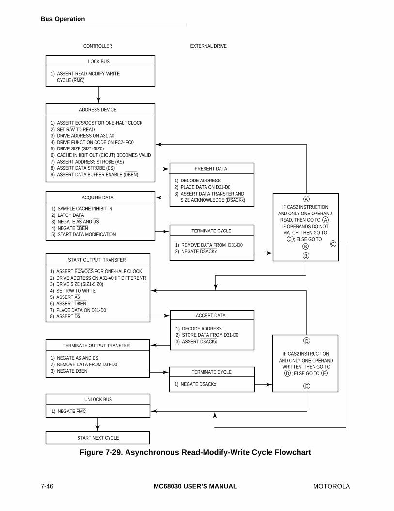
Bus Operation
7-46 MC68030 USER’S MANUAL MOTOROLA
Figure 7-29. Asynchronous Read-Modify-Write Cycle Flowchart
LOCK BUS
1) ASSERT READ-MODIFY-WRITE CYCLE (RMC)
ADDRESS DEVICE
1) ASSERT ECS/OCS FOR ONE-HALF CLOCK2) SET R/W TO READ3) DRIVE ADDRESS ON A31-A04) DRIVE FUNCTION CODE ON FC2- FC05) DRIVE SIZE (SIZ1-SIZ0)6) CACHE INHIBIT OUT (CIOUT) BECOMES VALID7) ASSERT ADDRESS STROBE (AS)8) ASSERT DATA STROBE (DS)9) ASSERT DATA BUFFER ENABLE (DBEN)
ACQUIRE DATA
2) LATCH DATA3) NEGATE AS AND DS4) NEGATE DBEN5) START DATA MODIFICATION
START OUTPUT TRANSFER
1) ASSERT ECS/OCS FOR ONE-HALF CLOCK2) DRIVE ADDRESS ON A31-A0 (IF DIFFERENT)3) DRIVE SIZE (SIZ1-SIZ0)4) SET R/W TO WRITE5) ASSERT AS6) ASSERT DBEN7) PLACE DATA ON D31-D08) ASSERT DS
TERMINATE OUTPUT TRANSFER
1) NEGATE AS AND DS2) REMOVE DATA FROM D31-D03) NEGATE DBEN
UNLOCK BUS
1) NEGATE RMC
START NEXT CYCLE
PRESENT DATA
1) DECODE ADDRESS2) PLACE DATA ON D31-D03) ASSERT DATA TRANSFER AND SIZE ACKNOWLEDGE (DSACKx)
TERMINATE CYCLE
1) REMOVE DATA FROM D31-D02) NEGATE DSACKx
ACCEPT DATA
1) DECODE ADDRESS2) STORE DATA FROM D31-D03) ASSERT DSACKx
TERMINATE CYCLE
A
IF CAS2 INSTRUCTIONAND ONLY ONE OPERANDREAD, THEN GO TO A ;IF OPERANDS DO NOTMATCH, THEN GO TO
C ; ELSE GO TOB C
B
1) NEGATE DSACKx
IF CAS2 INSTRUCTIONAND ONLY ONE OPERAND
WRITTEN, THEN GO TOD ; ELSE GO TO E
E
D
1) SAMPLE CACHE INHIBIT IN
CONTROLLER EXTERNAL DRIVE
Bus Operation
MOTOROLA MC68030 USER’S MANUAL 7-47
State 2
During state 2 (S2), the processor drives DBEN active to enable external data buffers. Theselected device uses R/W, SIZ0–SIZ1, A0–A1, and DS to place information on the databus. Any or all of the bytes (D24–D31, D16–D23, D8–D15, and D0–D7) are selected bySIZ0–SIZ1 and A0–A1. Concurrently, the selected device may assert the DSACKxsignals.
State 3
As long as at least one of the DSACKx signals is recognized by the end of S2 (meetingthe asynchronous input setup time requirement), data is latched on the next falling edgeof the clock, and the cycle terminates. If DSACKx is not recognized by the start of S3, theprocessor inserts wait states instead of proceeding to S4 and S5. To ensure that waitstates are inserted, both DSACK0 and DSACK1 must remain negated throughout theasynchronous input setup and hold times around the end of S2. If wait states are added,the processor continues to sample the DSACKx signals on the falling edges of the clockuntil one is recognized.
State 4
The processor samples the level of CIIN at the beginning of S4. At the end of S4, theprocessor latches the incoming data.
State 5
The processor negates AS, DS, and DBEN during S5. If more than one read cycle isrequired to read in the operand(s), S0–S5 are repeated for each read cycle. Whenfinished reading, the processor holds the address, R/W, and FC0–FC2 valid inpreparation for the write portion of the cycle.
The external device keeps its data and DSACKx signals asserted until it detects thenegation of AS or DS (whichever it detects first). The device must remove the data andnegate DSACKx within approximately one clock period after sensing the negation of ASor DS. DSACKx signals that remain asserted beyond this limit may be prematurelydetected for the next portion of the operation.
Idle States
The processor does not assert any new control signals during the idle states, but it mayinternally begin the modify portion of the cycle at this time. S6-S11 are omitted if no writecycle is required. If a write cycle is required, the R/W signal remains in the read mode untilS6 to prevent bus conflicts with the preceding read portion of the cycle; the data bus is notdriven until S8.
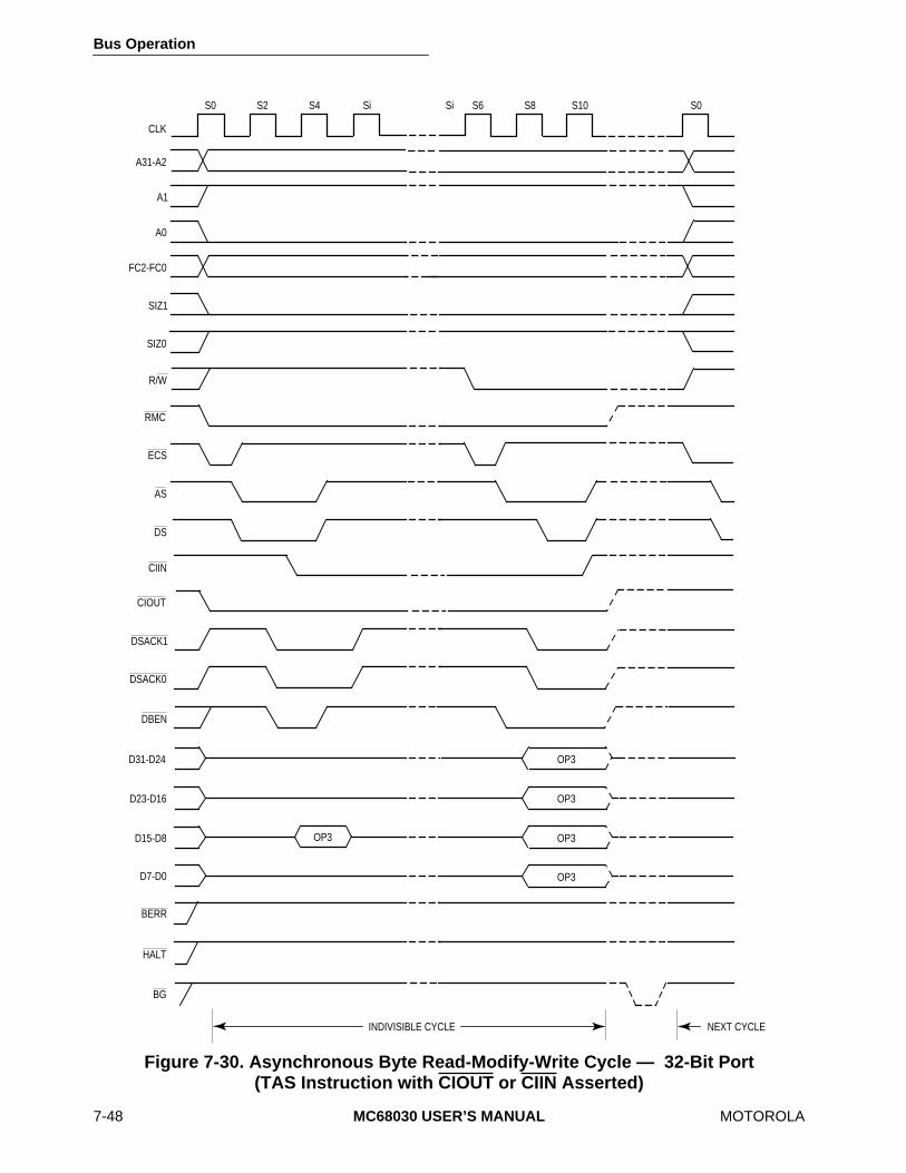
Bus Operation
7-48 MC68030 USER’S MANUAL MOTOROLA
Figure 7-30. Asynchronous Byte Read-Modify-Write Cycle — 32-Bit Port(TAS Instruction with CIOUT or CIIN Asserted)
Si
INDIVISIBLE CYCLE NEXT CYCLE
DS
DSACK0
DBEN
D31-D24
DSACK1
D7-D0
D23-D16
OP3
OP3
OP3
OP3
OP3
BERR
HALT
BG
D15-D8
AS
CLK
A31-A2
A1
A0
FC2-FC0
SIZ1
R/W
SIZ0
S0 S2 S4 Si S6 S8 S10 S0
RMC
ECS
CIIN
CIOUT
Bus Operation
MOTOROLA MC68030 USER’S MANUAL 7-49
State 6
The processor asserts ECS and OCS in S6 to indicate that another external cycle isbeginning. The processor drives R/W low for a write cycle. CIOUT also becomes valid,indicating the state of the MMU CI bit in the address translation descriptor or in a relevantTTx register. Depending on the write operation to be performed, the address lines maychange during S6.
State 7
In S7, the processor asserts AS, indicating that the address on the address bus is valid.The processor also asserts DBEN, which can be used to enable data buffers during S7.In addition, the ECS (and OCS, if asserted) signal is negated during S7.
State 8
During S8, the processor places the data to be written onto D0–D31.
State 9
The processor asserts DS during S9 indicating that the data is stable on the data bus. Aslong as at least one of the DSACKx signals is recognized by the end of S8 (meeting theasynchronous input setup time requirement), the cycle terminates one clock later. IfDSACKx is not recognized by the start of S9, the processor inserts wait states instead ofproceeding to S10 and S11. To ensure that wait states are inserted, both DSACK0 andDSACK1 must remain negated throughout the asynchronous input setup and hold timesaround the end of S8. If wait states are added, the processor continues to sampleDSACKx signals on the falling edges of the clock until one is recognized.
The selected device uses R/W, DS, SIZ0–SIZ1, and A0–A1 to latch data from the appropriate section(s) of the data bus (D24–D31, D16–D23, D8–D15, and D0–D7). SIZ0–SIZ1 and A0–A1 select the data bus sections. If it has not already done so, the device asserts DSACKx when it has successfully stored the data.
State 10
The processor issues no new control signals during S10.
Bus Operation
7-50 MC68030 USER’S MANUAL MOTOROLA
State 11
The processor negates AS and DS during S11. It holds the address and data valid duringS11 to provide address hold time for memory systems. R/W and FC0–FC2 also remainvalid throughout S11.
If more than one write cycle is required, S6-S11 are repeated for each write cycle.
The external device keeps DSACKx asserted until it detects the negation of AS or DS(whichever it detects first). The device must remove its data and negate DSACKx withinapproximately one clock period after sensing the negation of AS or DS.
7.3.4 Synchronous Read CycleA synchronous read cycle is terminated differently from an asynchronous read cycle;otherwise, the cycles assert and respond to the same signals, in the same sequence.STERM rather than DSACKx is asserted by the addressed external device to terminate asynchronous read cycle. Since STERM must meet the synchronous setup and hold timeswith respect to all rising edges of the clock while AS is asserted, it does not need to besynchronized by the processor. Only devices with 32-bit ports may assert STERM. STERMis also used with the CBREQ and CBACK signals during burst mode operation. It providesa two-clock (minimum) bus cycle for 32-bit ports and single-clock (minimum) burst accesses,although wait states can be inserted for these cycles as well. Therefore, a synchronouscycle terminated with STERM with one wait cycle is a three-clock bus cycle. However, notethat STERM is asserted one-half clock later than DSACKx would be for a similarasynchronous cycle with zero wait cycles (also three clocks). Thus, if dynamic bus sizing isnot needed, STERM can be used to provide more decision time in an external cache designthan is available with DSACKx for three-clock accesses.
Figure 7-31 is a flowchart of a synchronous long-word read cycle. Byte and word operationsare similar. Figure 7-32 is a functional timing diagram of a synchronous long-word readcycle.

Bus Operation
MOTOROLA MC68030 USER’S MANUAL 7-51
State 0
The read cycle starts with S0. The processor drives ECS low, indicating the beginning ofan external cycle. When the cycle is the first cycle of a read operand operation, OCS isdriven low at the same time. During S0, the processor places a valid address on A0–A31and valid function codes on FC0–FC2. The function codes select the address space forthe cycle. The processor drives R/W high for a read cycle and drives DBEN inactive todisable the data buffers. SIZ1-SIZ0 become valid, indicating the number of bytes to betransferred. CIOUT also becomes valid, indicating the state of the MMU CI bit in theaddress translation descriptor or in the appropriate TTx register.
State 1
One-half clock later in S1, the processor asserts AS, indicating that the address on theaddress bus is valid. The processor also asserts DS during S1. If the burst mode isenabled for the appropriate on-chip cache and all four long words of the cache entry areinvalid, (i.e., four long words can be read in), CBREQ is asserted. In addition, the ECS(and OCS, if asserted) signal is negated during S1.
Figure 7-31. Synchronous Long-Word Read Cycle Flowchart —No Burst Allowed
CONTROLLER
1) ASSERT ECS/OCS FOR ONE-HALF CLOCK 2) DRIVE R/W TO READ 3) DRIVE ADDRESS ON A31–A0 4) DRIVE FUNCTION ON FC2–FC0 5) DRIVE SIZE (SIZ1–SIZ0) (FOUR BYTES) 6) CACHE INHIBIT OUT (CIOUT) BECOMES VALID 7) ASSERT ADDRESS STROBE (AS) 8) ASSERT CACHE BURST REQUEST (CBREQ) (IF BURST POSSSIBLE) 9) ASSERT DATA STROBE (DS)10) ASSERT DATA BUFFER ENABLE (DBEN)
1) SAMPLE CACHE INHIBIT IN (CIIN) AND CACHE BURST ACKNOWLEDGE (CBACK)2) LATCH DATA3) NEGATE AS AND DS4) NEGATE DBEN
PRESENT DATA
1) DECODE ADDRESS2) PLACE DATA ON D31-D03) ASSERT SYNCHRONOUS TERMINATION (STERM)4) ASSERT CACHE BURST ACKNOWLEDGE (CBACK)
TERMINATE CYCLE
1) REMOVE DATA FROM D31-D02) NEGATE STERM
EXTERNAL DEVICE
ADDRESS DEVICE
ACQUIRE DATA
START NEXT CYCLE
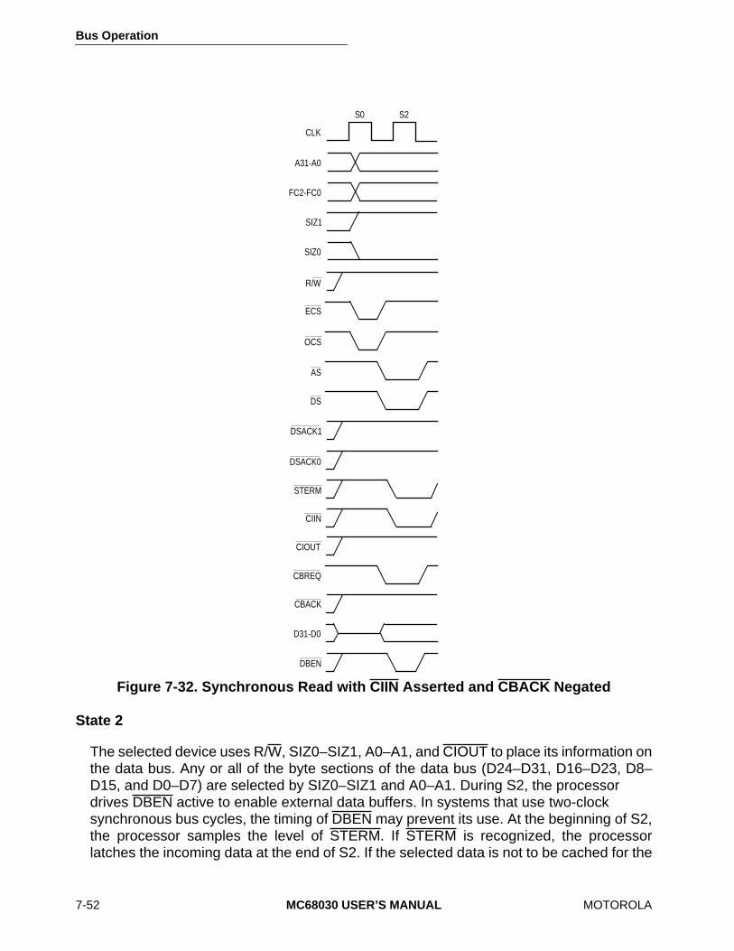
Bus Operation
7-52 MC68030 USER’S MANUAL MOTOROLA
State 2
The selected device uses R/W, SIZ0–SIZ1, A0–A1, and CIOUT to place its information onthe data bus. Any or all of the byte sections of the data bus (D24–D31, D16–D23, D8–D15, and D0–D7) are selected by SIZ0–SIZ1 and A0–A1. During S2, the processor drives DBEN active to enable external data buffers. In systems that use two-clock synchronous bus cycles, the timing of DBEN may prevent its use. At the beginning of S2,the processor samples the level of STERM. If STERM is recognized, the processorlatches the incoming data at the end of S2. If the selected data is not to be cached for the
Figure 7-32. Synchronous Read with CIIN Asserted and CBACK Negated
S0 S2
CLK
A31-A0
D31-D0
ECS
FC2-FC0
SIZ1
SIZ0
R/W
OCS
AS
DS
DSACK1
DSACK0
STERM
CIIN
CIOUT
CBREQ
CBACK
DBEN

Bus Operation
MOTOROLA MC68030 USER’S MANUAL 7-53
current cycle or if the device cannot supply 32 bits, CIIN must be asserted at the sametime as STERM. In addition, the state of CBACK is latched when STERM is recognized.
Since CIIN, CBACK, and STERM are synchronous signals, they must meet thesynchronous input setup and hold times for all rising edges of the clock while AS is asserted. If STERM is negated at the beginning of S2, wait states are inserted after S2,and STERM is sampled on every rising edge thereafter until it is recognized. OnceSTERM is recognized, data is latched on the next falling edge of the clock (corresponding to the beginning of S3).
State 3
The processor negates AS, DS, and DBEN during S3. It holds the address valid duringS3 to simplify memory interfaces. R/W, SIZ0–SIZ1, and FC0–FC2 also remain validthroughout S3.
The external device must keep its data asserted throughout the synchronous hold timefor data from the beginning of S3. The device must remove its data within one clockafter asserting STERM and negate STERM within two clocks after asserting STERM;otherwise, the processor may inadvertently use STERM for the next bus cycle.
7.3.5 Synchronous Write CycleA synchronous write cycle is terminated differently from an asynchronous write cycle andthe data strobe may not be useful. Otherwise, the cycles assert and respond to the samesignal, in the same sequence. STERM is asserted by the external device to terminate asynchronous write cycle. The discussion of STERM in the preceding section applies to writecycles as well as to read cycles.
DS is not asserted for two-clock synchronous write cycles; therefore, the clock (CLK) maybe used as the timing signal for latching the data. In addition, there is no time from the latestassertion of AS and the required assertion of STERM for any two-clock synchronous buscycle. The system must qualify a memory write with the assertion of AS to ensure that thewrite is not aborted by internal conditions within the MC68030.
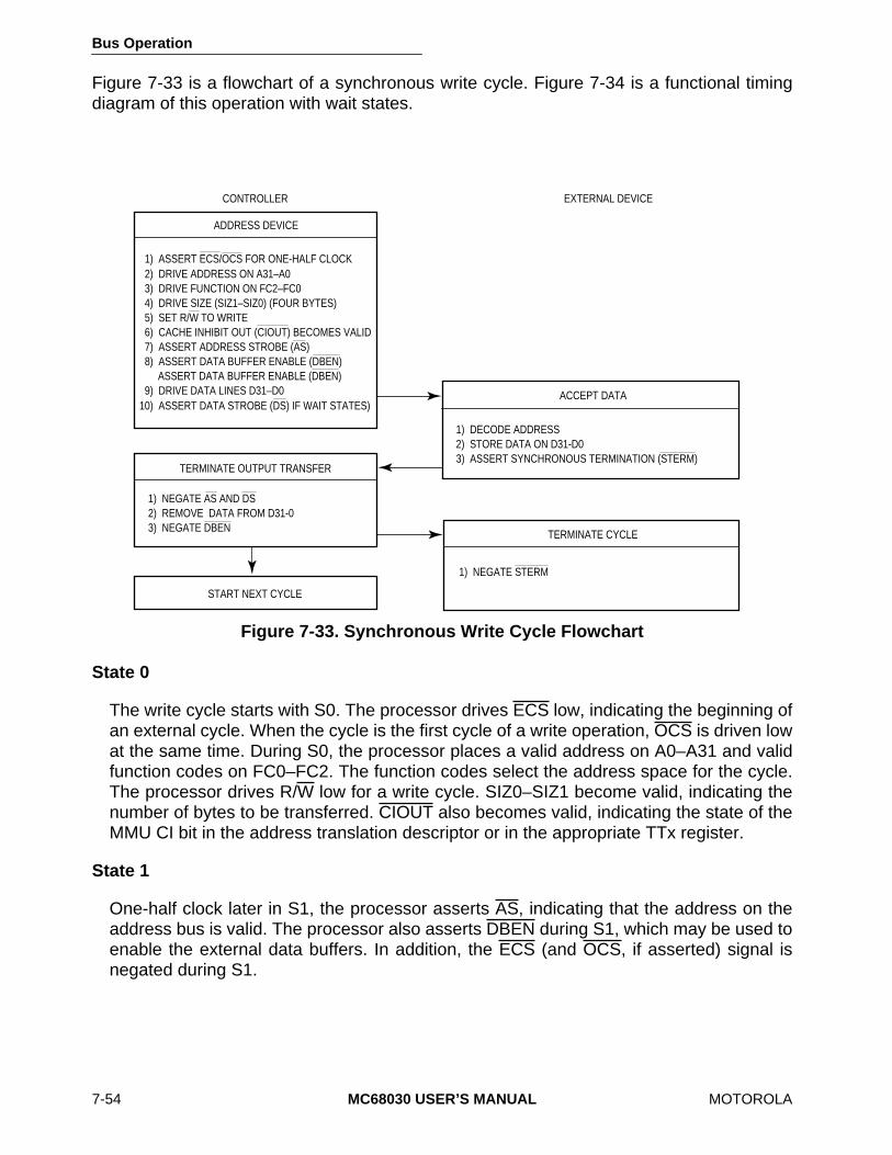
Bus Operation
7-54 MC68030 USER’S MANUAL MOTOROLA
Figure 7-33 is a flowchart of a synchronous write cycle. Figure 7-34 is a functional timingdiagram of this operation with wait states.
State 0
The write cycle starts with S0. The processor drives ECS low, indicating the beginning ofan external cycle. When the cycle is the first cycle of a write operation, OCS is driven lowat the same time. During S0, the processor places a valid address on A0–A31 and validfunction codes on FC0–FC2. The function codes select the address space for the cycle.The processor drives R/W low for a write cycle. SIZ0–SIZ1 become valid, indicating thenumber of bytes to be transferred. CIOUT also becomes valid, indicating the state of theMMU CI bit in the address translation descriptor or in the appropriate TTx register.
State 1
One-half clock later in S1, the processor asserts AS, indicating that the address on theaddress bus is valid. The processor also asserts DBEN during S1, which may be used toenable the external data buffers. In addition, the ECS (and OCS, if asserted) signal isnegated during S1.
Figure 7-33. Synchronous Write Cycle Flowchart
CONTROLLER
1) ASSERT ECS/OCS FOR ONE-HALF CLOCK 2) DRIVE ADDRESS ON A31–A0 3) DRIVE FUNCTION ON FC2–FC0 4) DRIVE SIZE (SIZ1–SIZ0) (FOUR BYTES) 5) SET R/W TO WRITE 6) CACHE INHIBIT OUT (CIOUT) BECOMES VALID 7) ASSERT ADDRESS STROBE (AS) 8) ASSERT DATA BUFFER ENABLE (DBEN) ASSERT DATA BUFFER ENABLE (DBEN) 9) DRIVE DATA LINES D31–D010) ASSERT DATA STROBE (DS) IF WAIT STATES)
1) NEGATE AS AND DS2) REMOVE DATA FROM D31-03) NEGATE DBEN
1) DECODE ADDRESS2) STORE DATA ON D31-D03) ASSERT SYNCHRONOUS TERMINATION (STERM)
TERMINATE CYCLE
1) NEGATE STERM
EXTERNAL DEVICE
ADDRESS DEVICE
START NEXT CYCLE
TERMINATE OUTPUT TRANSFER
ACCEPT DATA
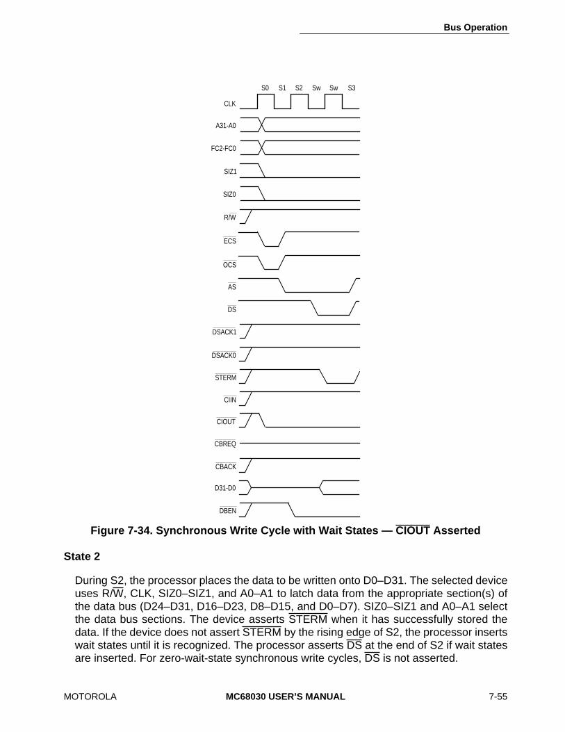
Bus Operation
MOTOROLA MC68030 USER’S MANUAL 7-55
State 2
During S2, the processor places the data to be written onto D0–D31. The selected deviceuses R/W, CLK, SIZ0–SIZ1, and A0–A1 to latch data from the appropriate section(s) ofthe data bus (D24–D31, D16–D23, D8–D15, and D0–D7). SIZ0–SIZ1 and A0–A1 selectthe data bus sections. The device asserts STERM when it has successfully stored thedata. If the device does not assert STERM by the rising edge of S2, the processor insertswait states until it is recognized. The processor asserts DS at the end of S2 if wait statesare inserted. For zero-wait-state synchronous write cycles, DS is not asserted.
Figure 7-34. Synchronous Write Cycle with Wait States — CIOUT Asserted
CLK
A31-A0
D31-D0
ECS
FC2-FC0
SIZ1
SIZ0
R/W
OCS
AS
DS
DSACK1
DSACK0
STERM
CIIN
CIOUT
CBREQ
CBACK
DBEN
S0 S2 SwS1 Sw S3
Bus Operation
7-56 MC68030 USER’S MANUAL MOTOROLA
State 3
The processor negates AS (and DS, if necessary) during S3. It holds the address and datavalid during S3 to simplify memory interfaces. R/W, SIZ0–SIZ1, FC0–FC2, and DBENalso remain valid throughout S3.
The addressed device must negate STERM within two clock periods after asserting it, orthe processor may use STERM for the next bus cycle.
7.3.6 Synchronous Read-Modify-Write CycleA synchronous read-modify-write operation differs from an asynchronous read-modify-writeoperation only in the terminating signal of the read and write cycles and in the use of CLKinstead of DS latching data in the write cycle. Like the asynchronous operation, thesynchronous read-modify-write operation is indivisible. Although the operation issynchronous, the burst mode is never used during read-modify-write cycles.
Figure 7-35 is a flowchart of the synchronous read-modify-write operation. Timing for thecycle is shown in Figure 7-36.
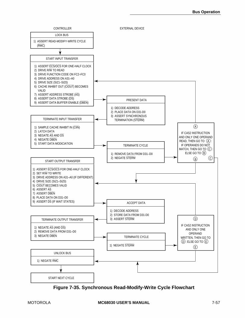
Bus Operation
MOTOROLA MC68030 USER’S MANUAL 7-57
Figure 7-35. Synchronous Read-Modify-Write Cycle Flowchart
1) ASSERT READ-MODIFY-WRITE CYCLE (RMC)
LOCK BUS
CONTROLLER
START INPUT TRANSFER
1) ASSERT ECS/OCS FOR ONE-HALF CLOCK2) DRIVE R/W TO READ3) DRIVE FUNCTION CODE ON FC2–FC04) DRIVE ADDRESS ON A31–A05) DRIVE SIZE (SIZ1–SIZ0)6) CACHE INHIBIT OUT (CIOUT) BECOMES VALID7) ASSERT ADDRESS STROBE (AS)8) ASSERT DATA STROBE (DS)9) ASSERT DATA BUFFER ENABLE (DBEN)
TERMINATE INPUT TRANSFER
1) SAMPLE CACHE INHIBIT IN (CIIN)2) LATCH DATA3) NEGATE AS AND DS4) NEGATE DBEN5) START DATA MODICIATION
START OUTPUT TRANSFER
1) ASSERT ECS/OCS FOR ONE-HALF CLOCK2) SET R/W TO WRITE3) DRIVE ADDRESS ON A31–A0 (IF DIFFERENT)4) DRIVE SIZE (SIZ1–SIZ0)5) CIOUT BECOMES VALID6) ASSERT AS7) ASSERT DBEN8) PLACE DATA ON D31–D09) ASSERT DS (IF WAIT STATES)
TERMINATE OUTPUT TRANSFER
1) NEGATE AS (AND DS)2) REMOVE DATA FROM D31–D03) NEGATE DBEN
UNLOCK BUS
1) NEGATE RMC
START NEXT CYCLE
PRESENT DATA
1) DECODE ADDRESS2) PLACE DATA ON D31-D03) ASSERT SYNCHRONOUS TERMINATION (STERM)
TERMINATE CYCLE
1) REMOVE DATA FROM D31–D02) NEGATE STERM
ACCEPT DATA
TERMINATE CYCLE
1) DECODE ADDRESS2) STORE DATA FROM D31-D03) ASSERT STERM
1) NEGATE STERM
IF CAS2 INSTRUCTIONAND ONLY ONE
OPERANDWRITTEN, THEN GO TO D : ELSE GO TO E
E
D
IF CAS2 INSTRUCTIONAND ONLY ONE OPERANDREAD, THEN GO TO A :
IF OPERANDS DO NOTMATCH, THEN GO TO C :
ELSE GO TO B
A
CB
EXTERNAL DEVICE
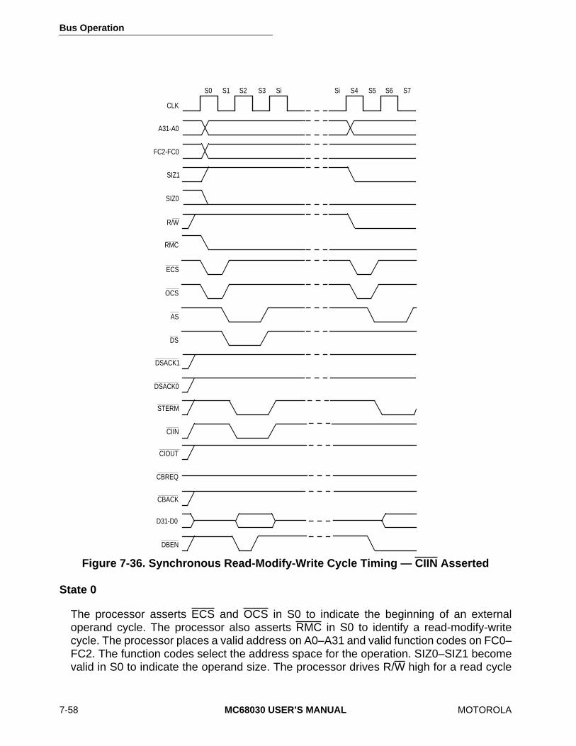
Bus Operation
7-58 MC68030 USER’S MANUAL MOTOROLA
State 0
The processor asserts ECS and OCS in S0 to indicate the beginning of an externaloperand cycle. The processor also asserts RMC in S0 to identify a read-modify-writecycle. The processor places a valid address on A0–A31 and valid function codes on FC0–FC2. The function codes select the address space for the operation. SIZ0–SIZ1 becomevalid in S0 to indicate the operand size. The processor drives R/W high for a read cycle
Figure 7-36. Synchronous Read-Modify-Write Cycle Timing — CIIN Asserted
S0 S2 SiS1 S3 Si S4 S5 S6 S7
CLK
A31-A0
D31-D0
ECS
FC2-FC0
SIZ1
SIZ0
R/W
OCS
AS
DS
DSACK1
DSACK0
STERM
CIIN
CIOUT
CBREQ
CBACK
DBEN
RMC
Bus Operation
MOTOROLA MC68030 USER’S MANUAL 7-59
and sets CIOUT to the value of the MMU CI bit in the address translation descriptor or inthe appropriate TTx register. The processor drives DBEN inactive to disable the databuffers.
State 1
One-half clock later in S1, the processor asserts AS, indicating that the address on theaddress bus is valid. The processor also asserts DS during S1. In addition, the ECS (andOCS, if asserted) signal is negated during S1.
State 2
The selected device uses R/W, SIZ0–SIZ1, A0–A1, and CIOUT to place its information onthe data bus. Any or all of the byte sections (D24–D31, D16–D23, D8–D15, and D0–D7)are selected by SIZ0–SIZ1 and A0–A1. During S2, the processor drives DBEN active toenable external data buffers. In systems that use two-clock synchronous bus cycles, thetiming of DBEN may prevent its use. At the beginning of S2, the processor samples thelevel of STERM. If STERM is recognized, the processor latches the incoming data. If theselected data is not to be cached for the current cycle or if the device cannot supply 32bits, CIIN must be asserted at the same time as STERM.
Since CIIN and STERM are synchronous signals, they must meet the synchronous nputsetup and hold times for all rising edges of the clock while AS is asserted. If STERM isnegated at the beginning of S2, wait states are inserted after S2, and STERM is sampledon every rising edge thereafter until it is recognized. Once STERM is recognized, data islatched on the next falling edge of the clock (corresponding to the beginning of S3).
Bus Operation
7-60 MC68030 USER’S MANUAL MOTOROLA
State 3
The processor negates AS, DS, and DBEN during S3. If more than one read cycle isrequired to read in the operand(s), S0–S3 are repeated accordingly. When finished withthe read cycle, the processor holds the address, R/W, and FC0–FC2 valid in preparationfor the write portion of the cycle.
The external device must keep its data asserted throughout the synchronous hold time fordata from the beginning of S3. The device must remove the data within one-clock cycleafter asserting STERM to avoid bus contention. It must also negate STERM within twoclocks after asserting STERM; otherwise, the processor may inadvertently use STERMfor the next bus cycle.
Idle States
The processor does not assert any new control signals during the idle states, but it maybegin the modify portion of the cycle at this time. The R/W signal remains in the read modeuntil S4 to prevent bus conflicts with the preceding read portion of the cycle; the data busis not driven until S6.
State 4
The processor asserts ECS and OCS in S4 to indicate that an external cycle is beginning.The processor drives R/W low for a write cycle. CIOUT also becomes valid, indicating thestate of the MMU CI bit in the address translation descriptor or in the appropriate TTxregister. Depending on the write operation to be performed, the address lines may changeduring S4.
State 5
In state 5 (S5), the processor asserts AS to indicate that the address on the address busis valid. The processor also asserts DBEN during S5, which can be used to enableexternal data buffers.
State 6
During S6, the processor places the data to be written onto the D0–D31.
The selected device uses R/W, CLK, SIZ0–SIZ1, and A0–A1 to latch data from theappropriate byte(s) of the data bus (D24–D31, D16–D23, D8–D15, and D0–D7). SIZ0–SIZ1 and A0–A1 select the data bus sections. The device asserts STERM when it hassuccessfully stored the data. If the device does not assert STERM by the rising edge ofS6, the processor inserts wait states until it is recognized. The processor asserts DS atthe end of S6 if wait states are inserted. Note that for zero-wait-state synchronous writecycles, DS is not asserted.

Bus Operation
MOTOROLA MC68030 USER’S MANUAL 7-61
State 7
The processor negates AS (and DS, if necessary) during S7. It holds the address and data valid during S7 to simplify memory interfaces. R/W and FC0–FC2 also remain valid throughout S7.
If more than one write cycle is required, S8-S11 are repeated for each write cycle.
The external device must negate STERM within two clock periods after asserting it, or theprocessor may inadvertently use STERM for the next bus cycle.
7.3.7 Burst Operation CyclesThe MC68030 supports a burst mode for filling the on-chip instruction and data caches.
The MC68030 provides a set of handshake control signals for the burst mode. When a missoccurs in one of the caches, the MC68030 initiates a bus cycle to obtain the required dataor instruction stream fetch. If the data or instruction can be cached, the MC68030 attemptsto fill a cache entry. Depending on the alignment for a data access, the MC68030 mayattempt to fill two cache entries. The processor may also assert CBREQ to request a burstfill operation. That is, the processor can fill additional entries in the line. The MC68030 allowsa burst of as many as four long words.
The mechanism that asserts the CBREQ signal for burstable cache entries is enabled bythe data burst enable (DBE) and instruction burst enable (IBE) bits of the cache controlregister (CACR) for the data and instruction caches, respectively. Either of the followingconditions cause the MC68030 to initiate a cache burst request (and assert CBREQ) for acachable read cycle:
• The logical address and function code signals of the current instruction or data fetch do not match the indexed tag field in the respective instruction or data cache.
• All four long words corresponding to the indexed tag in the appropriate cache are marked invalid.
However, the MC68030 does not assert CBREQ during the first portion of a misalignedaccess if the remainder of the access does not correspond to the same cache line. Refer to6.1.3.1 Single Entry Mode for details.
Bus Operation
7-62 MC68030 USER’S MANUAL MOTOROLA
If the appropriate cache is not enabled or if the cache freeze bit for the cache is set, theprocessor does not assert CBREQ. CBREQ is not asserted during the read or write cyclesof any read-modify-write operation.
The MC68030 allows burst filling only from 32-bit ports that terminate bus cycles withSTERM and respond to CBREQ by asserting CBACK. When the MC68030 recognizesSTERM and CBACK and it has asserted CBREQ, it maintains AS, DS, R/W, A0–A31, FC0–FC2, SIZ0–SIZ1 in their current state throughout the burst operation. The processorcontinues to accept data on every clock during which STERM is asserted until the burst iscomplete or an abnormal termination occurs.
CBACK indicates that the addressed device can respond to a cache burst request bysupplying one more long word of data in the burst mode. It can be asserted independentlyof the CBREQ signal, and burst mode is only initiated if both of these signals are assertedfor a synchronous cycle. If the MC68030 executes a full burst operation and fetches fourlong words, CBREQ is negated after STERM is asserted for the third cycle, indicating thatthe MC68030 only requests one more long word (the fourth cycle). CBACK can then benegated, and the MC68030 latches the data for the fourth cycle and completes the cacheline fill.
The following conditions can abort a burst fill:
• CIIN asserted,
• BERR asserted, or
• CBACK negated prematurely.
The processing of a bus error during a burst fill operation is described in 7.5.1 Bus Errors.
For the purposes of halting the processor or arbitrating the bus away from the processor withBR, a burst operation is a single cycle since AS remains asserted during the entireoperation. If the HALT signal is asserted during a burst operation, the processor halts at theend of the operation. Refer to 7.5.3 Halt Operation for more information about the haltoperation. An alternate bus master requesting the bus with BR may become bus master atthe end of the operation provided BR is asserted early enough to be internally synchronizedbefore another processor cycle begins. Refer to 7.7 Bus Arbitration for more informationabout bus arbitration.
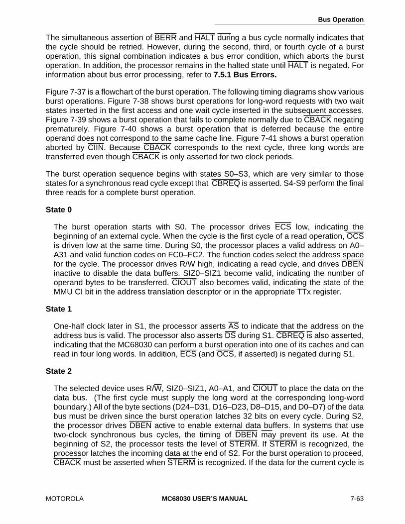
Bus Operation
MOTOROLA MC68030 USER’S MANUAL 7-63
The simultaneous assertion of BERR and HALT during a bus cycle normally indicates thatthe cycle should be retried. However, during the second, third, or fourth cycle of a burstoperation, this signal combination indicates a bus error condition, which aborts the burstoperation. In addition, the processor remains in the halted state until HALT is negated. Forinformation about bus error processing, refer to 7.5.1 Bus Errors.
Figure 7-37 is a flowchart of the burst operation. The following timing diagrams show variousburst operations. Figure 7-38 shows burst operations for long-word requests with two waitstates inserted in the first access and one wait cycle inserted in the subsequent accesses.Figure 7-39 shows a burst operation that fails to complete normally due to CBACK negatingprematurely. Figure 7-40 shows a burst operation that is deferred because the entireoperand does not correspond to the same cache line. Figure 7-41 shows a burst operationaborted by CIIN. Because CBACK corresponds to the next cycle, three long words aretransferred even though CBACK is only asserted for two clock periods.
The burst operation sequence begins with states S0–S3, which are very similar to thosestates for a synchronous read cycle except that CBREQ is asserted. S4-S9 perform the finalthree reads for a complete burst operation.
State 0
The burst operation starts with S0. The processor drives ECS low, indicating thebeginning of an external cycle. When the cycle is the first cycle of a read operation, OCSis driven low at the same time. During S0, the processor places a valid address on A0–A31 and valid function codes on FC0–FC2. The function codes select the address spacefor the cycle. The processor drives R/W high, indicating a read cycle, and drives DBENinactive to disable the data buffers. SIZ0–SIZ1 become valid, indicating the number ofoperand bytes to be transferred. CIOUT also becomes valid, indicating the state of theMMU CI bit in the address translation descriptor or in the appropriate TTx register.
State 1
One-half clock later in S1, the processor asserts AS to indicate that the address on theaddress bus is valid. The processor also asserts DS during S1. CBREQ is also asserted,indicating that the MC68030 can perform a burst operation into one of its caches and canread in four long words. In addition, ECS (and OCS, if asserted) is negated during S1.
State 2
The selected device uses R/W, SIZ0–SIZ1, A0–A1, and CIOUT to place the data on thedata bus. (The first cycle must supply the long word at the corresponding long-wordboundary.) All of the byte sections (D24–D31, D16–D23, D8–D15, and D0–D7) of the databus must be driven since the burst operation latches 32 bits on every cycle. During S2,the processor drives DBEN active to enable external data buffers. In systems that usetwo-clock synchronous bus cycles, the timing of DBEN may prevent its use. At thebeginning of S2, the processor tests the level of STERM. If STERM is recognized, theprocessor latches the incoming data at the end of S2. For the burst operation to proceed,CBACK must be asserted when STERM is recognized. If the data for the current cycle is
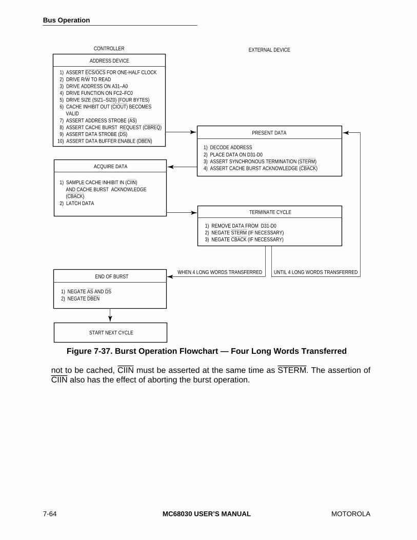
Bus Operation
7-64 MC68030 USER’S MANUAL MOTOROLA
not to be cached, CIIN must be asserted at the same time as STERM. The assertion ofCIIN also has the effect of aborting the burst operation.
Figure 7-37. Burst Operation Flowchart — Four Long Words Transferred
END OF BURST
1) NEGATE AS AND DS2) NEGATE DBEN
CONTROLLER
1) ASSERT ECS/OCS FOR ONE-HALF CLOCK2) DRIVE R/W TO READ3) DRIVE ADDRESS ON A31–A04) DRIVE FUNCTION ON FC2–FC05) DRIVE SIZE (SIZ1–SIZ0) (FOUR BYTES)6) CACHE INHIBIT OUT (CIOUT) BECOMES VALID7) ASSERT ADDRESS STROBE (AS)8) ASSERT CACHE BURST REQUEST (CBREQ)9) ASSERT DATA STROBE (DS)
10) ASSERT DATA BUFFER ENABLE (DBEN)
1) SAMPLE CACHE INHIBIT IN (CIIN) AND CACHE BURST ACKNOWLEDGE (CBACK)2) LATCH DATA
PRESENT DATA
1) DECODE ADDRESS2) PLACE DATA ON D31-D03) ASSERT SYNCHRONOUS TERMINATION (STERM)4) ASSERT CACHE BURST ACKNOWLEDGE (CBACK)
TERMINATE CYCLE
1) REMOVE DATA FROM D31-D02) NEGATE STERM (IF NECESSARY)3) NEGATE CBACK (IF NECESSARY)
EXTERNAL DEVICE
ADDRESS DEVICE
ACQUIRE DATA
WHEN 4 LONG WORDS TRANSFERRED UNTIL 4 LONG WORDS TRANSFERRED
START NEXT CYCLE

Bus Operation
MOTOROLA MC68030 USER’S MANUAL 7-65
Figure 7-38. Long-Word Operand Request from $07 withBurst Request and Wait Cycle
S0 S2 SwS1 Sw Sw Sw SwS4 S5 Sw SwS6 S9S8SwS7
b4–b7 bC–bFbC–bFb8–bB
SwSw SwSw S3
A31-A4
A3
A2–A0
FC2-FC0
R/W
ECS
OCS
CLK
AS
DS
STERM
CBREQ
CBACK
D31–D0
DBEN
SIZ1–SIZ0
CIIN
CIOUT
01 10 11 00
VALUE OF A3:A2 INCREMENTED BY THE SYSTEM HARDWARE
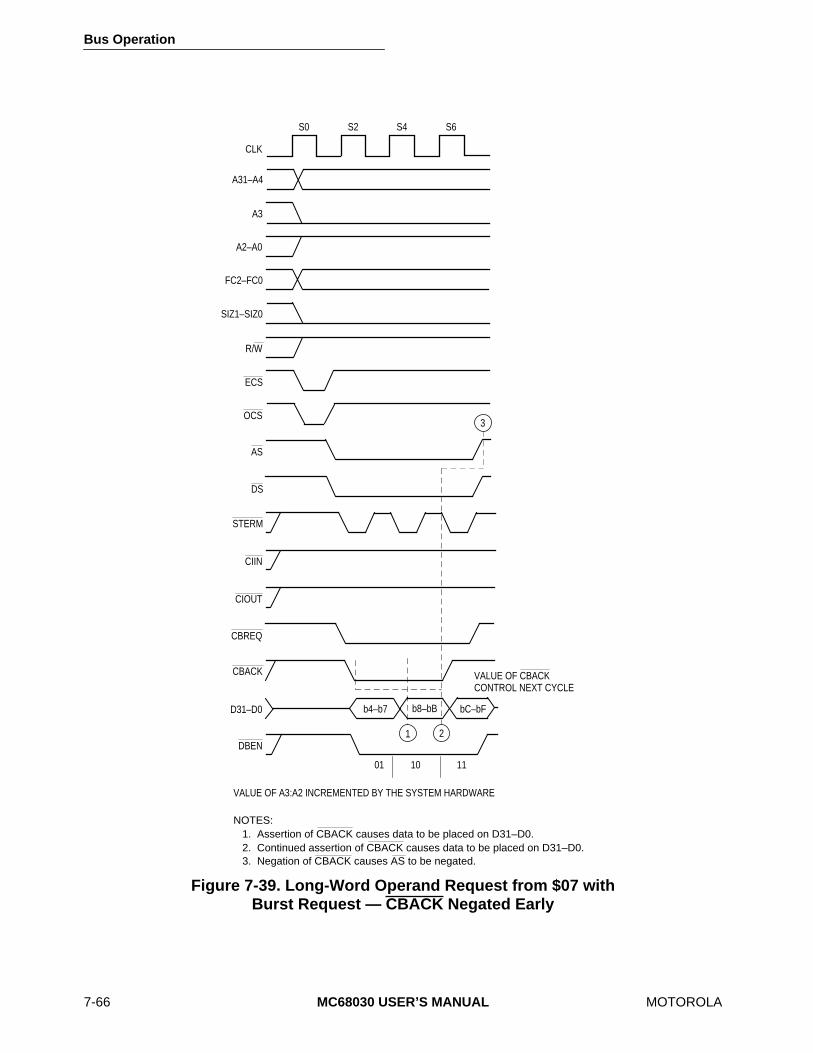
Bus Operation
7-66 MC68030 USER’S MANUAL MOTOROLA
Figure 7-39. Long-Word Operand Request from $07 withBurst Request — CBACK Negated Early
CLK
A31–A4
A3
A2–A0
FC2–FC0
SIZ1–SIZ0
R/W
S0 S2 S4 S6
ECS
OCS
AS
DS
b4–b7 b8–bB bC–bF
01 10 11
1 2
VALUE OF CBACKCONTROL NEXT CYCLE
3
STERM
CIIN
CIOUT
CBREQ
CBACK
D31–D0
DBEN
VALUE OF A3:A2 INCREMENTED BY THE SYSTEM HARDWARE
NOTES: 1. Assertion of CBACK causes data to be placed on D31–D0. 2. Continued assertion of CBACK causes data to be placed on D31–D0. 3. Negation of CBACK causes AS to be negated.
Bus Operation
MOTOROLA MC68030 USER’S MANUAL 7-67
Figure 7-40. Long-Word Operand Request from $0E — Burst Fill Deferred
A31-A5
A4
A3–A1
FC2-FC0
SIZ1
R/W
ECS
OCS
CLK
S0 S2 Sw S0S1 Sw S3 S1 S2 Sw Sw S3 Sw Sw S4 S5 Sw Sw S6 S9S8SwSwS7
A0
SIZ0
AS
DS
STERM
CBREQ
CBACK
D31–D0
DBEN
b4–b7 bC–bFbC–bF b0–b3 b8–bB
PREVIOUS CACHE BLOCK NEXT CACHE BLOCK - START BURST CYCLE
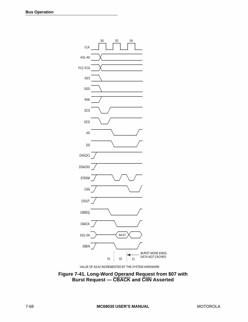
Bus Operation
7-68 MC68030 USER’S MANUAL MOTOROLA
Figure 7-41. Long-Word Operand Request from $07 with Burst Request — CBACK and CIIN Asserted
A31–A0
FC2–FC0
R/W
ECS
OCS
CLK
S0 S2
AS
DS
STERM
CBREQ
CBACK
D31–D0
DBEN
CIIN
CIOUT
S4
SIZ1
SIZ0
DSACK1
DSACK0
b4-b7
BURST MODE ENDS,DATA NOT CACHED
01 10 11
VALUE OF A3:A2 INCREMENTED BY THE SYSTEM HARDWARE
Bus Operation
MOTOROLA MC68030 USER’S MANUAL 7-69
Since CIIN, CBACK, and STERM are synchronous signals, they must meet thesynchronous input setup and hold times for all rising edges of the clock while AS isasserted. If STERM is negated at the beginning of S2, wait states are inserted after S2,and STERM is sampled on every rising edge of the clock thereafter until it is recognized.Once STERM is recognized, data is latched on the next falling edge of the clock(corresponding to the beginning of S3).
State 3
The processor maintains AS, DS, and DBEN asserted during S3. It also holds the addressvalid during S3 for continuation of the burst. R/W, SIZ0–SIZ1, and FC0–FC2 also remainvalid throughout S3.
The external device must keep the data driven throughout the synchronous hold time fordata from the beginning of S3. The device must negate STERM within one clock afterasserting STERM; otherwise, the processor may inadvertently use STERM prematurelyfor the next burst access. STERM need not be negated if subsequent accesses do notrequire wait cycles.
State 4
At the beginning of S4, the processor tests the level of STERM. This state signifies thebeginning of burst mode, and the remaining states correspond to burst fill cycles. IfSTERM is recognized, the processor latches the incoming data at the end of S4. This datacorresponds to the second long word of the burst. If STERM is negated at the beginningof S4, wait states are inserted instead of S4 and S5, and STERM is sampled on everyrising edge of the clock thereafter until it is recognized. As for synchronous cycles, thestates of CBACK and CIIN are latched at the time STERM is recognized. The assertionof CBACK at this time indicates that the burst operation should continue, and the assertionof CIIN indicates that the data latched at the end of S4 should not be cached and that theburst should abort.
State 5
The processor maintains all the signals on the bus driven throughout S5 for continuationof the burst. The same hold times for STERM and data described for S3 apply here.
State 6
This state is identical to S4 except that once STERM is recognized, the third long word ofdata for the burst is latched at the end of S6.
Bus Operation
7-70 MC68030 USER’S MANUAL MOTOROLA
State 7
During this state, the processor negates CBREQ, and the memory device may negate CBACK. Aside from this, all other bus signals driven by the processor remain driven. The same hold times for STERM and data described for S3 apply here.
State 8
This state is identical to S4 except that CBREQ is negated, indicating that the processorcannot continue to accept more data after this. The data latched at the end of S8corresponds to the fourth long word of the burst.
State 9
The processor negates AS, DS, and DBEN during S9. It holds the address, R/W, SIZ0–SIZ1, and FC0–FC2 valid throughout S9. The same hold times for data described for S3apply here.
Note that the address bus of the MC68030 remains driven to a constant value for theduration of a burst transfer operation (including the first transfer before burst mode isentered). If an external memory system requires incrementing of the long-word baseaddress to supply successive long words of information, this function must be performed byexternal hardware. Additionally, in the case of burst transfers that cross a 16-byte boundary(i.e., the first long word transferred is not located at A3/A2=00), the external hardware mustcorrectly control the continuation or termination of the burst transfer as desired. The burstmay be terminated by negating CBACK during the transfer of the most significant long wordof the 16-byte image (A3/A2=11) or may be continued (with CBACK asserted) by providingthe long word located at A3/A2=00 (i.e., the count sequence wraps back to zero andcontinues as necessary). The MC68030 caches assume the higher order address lines (A4-A31) remain unchanged as the long-word accesses wrap back around to A3/A2=00.
7.4 CPU SPACE CYCLESFC0–FC2 select user and supervisor program and data areas as listed in Table 4-1. Thearea selected by FC0–FC2=$7 is classified as the CPU space. The interrupt acknowledge,breakpoint acknowledge, and coprocessor communication cycles described in the followingsections utilize CPU space.
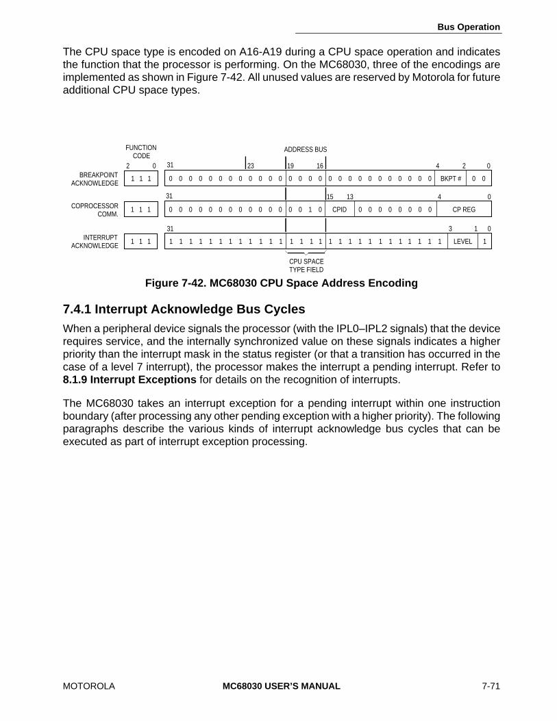
Bus Operation
MOTOROLA MC68030 USER’S MANUAL 7-71
The CPU space type is encoded on A16-A19 during a CPU space operation and indicatesthe function that the processor is performing. On the MC68030, three of the encodings areimplemented as shown in Figure 7-42. All unused values are reserved by Motorola for futureadditional CPU space types.
7.4.1 Interrupt Acknowledge Bus CyclesWhen a peripheral device signals the processor (with the IPL0–IPL2 signals) that the devicerequires service, and the internally synchronized value on these signals indicates a higherpriority than the interrupt mask in the status register (or that a transition has occurred in thecase of a level 7 interrupt), the processor makes the interrupt a pending interrupt. Refer to8.1.9 Interrupt Exceptions for details on the recognition of interrupts.
The MC68030 takes an interrupt exception for a pending interrupt within one instructionboundary (after processing any other pending exception with a higher priority). The followingparagraphs describe the various kinds of interrupt acknowledge bus cycles that can beexecuted as part of interrupt exception processing.
Figure 7-42. MC68030 CPU Space Address Encoding
1 1 1
1 1 1
1 1 1
BREAKPOINTACKNOWLEDGE
COPROCESSORCOMM.
INTERRUPTACKNOWLEDGE
1 1 1 1 1 1 1 1 1 1 1 1 1 1 1 1 1 1 1 1 1 1 1 1 1 1 1 1 LEVEL 1
0 0 0 0 0 0 0 0 0 0 0 0 0 0 1 0 CPID 0 0 0 0 0 0 0 0 CP REG
15 13 4 0
3 1 031
31
BKPT # 0 0
31 4 2 0
0 0 0 0 0 0 0 0 0 0 00 0 0 0 0 0 0 0 0 0 0 0 0 0 0 0
19 16232 0
FUNCTIONCODE
ADDRESS BUS
CPU SPACETYPE FIELD
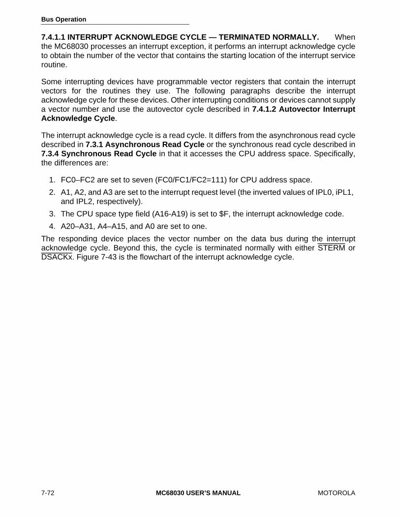
Bus Operation
7-72 MC68030 USER’S MANUAL MOTOROLA
7.4.1.1 INTERRUPT ACKNOWLEDGE CYCLE — TERMINATED NORMALLY. Whenthe MC68030 processes an interrupt exception, it performs an interrupt acknowledge cycleto obtain the number of the vector that contains the starting location of the interrupt serviceroutine.
Some interrupting devices have programmable vector registers that contain the interruptvectors for the routines they use. The following paragraphs describe the interruptacknowledge cycle for these devices. Other interrupting conditions or devices cannot supplya vector number and use the autovector cycle described in 7.4.1.2 Autovector InterruptAcknowledge Cycle.
The interrupt acknowledge cycle is a read cycle. It differs from the asynchronous read cycledescribed in 7.3.1 Asynchronous Read Cycle or the synchronous read cycle described in7.3.4 Synchronous Read Cycle in that it accesses the CPU address space. Specifically,the differences are:
1. FC0–FC2 are set to seven (FC0/FC1/FC2=111) for CPU address space.
2. A1, A2, and A3 are set to the interrupt request level (the inverted values of IPL0, iPL1, and IPL2, respectively).
3. The CPU space type field (A16-A19) is set to $F, the interrupt acknowledge code.
4. A20–A31, A4–A15, and A0 are set to one.
The responding device places the vector number on the data bus during the interruptacknowledge cycle. Beyond this, the cycle is terminated normally with either STERM orDSACKx. Figure 7-43 is the flowchart of the interrupt acknowledge cycle.
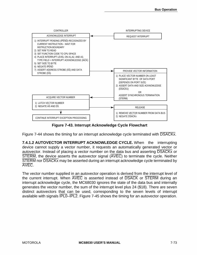
Bus Operation
MOTOROLA MC68030 USER’S MANUAL 7-73
Figure 7-44 shows the timing for an interrupt acknowledge cycle terminated with DSACKx.
7.4.1.2 AUTOVECTOR INTERRUPT ACKNOWLEDGE CYCLE. When the interruptingdevice cannot supply a vector number, it requests an automatically generated vector orautovector. Instead of placing a vector number on the data bus and asserting DSACKx orSTERM, the device asserts the autovector signal (AVEC) to terminate the cycle. NeitherSTERM nor DSACKx may be asserted during an interrupt acknowledge cycle terminated byAVEC.
The vector number supplied in an autovector operation is derived from the interrupt level ofthe current interrupt. When AVEC is asserted instead of DSACK or STERM during aninterrupt acknowledge cycle, the MC68030 ignores the state of the data bus and internallygenerates the vector number, the sum of the interrupt level plus 24 ($18). There are sevendistinct autovectors that can be used, corresponding to the seven levels of interruptavailable with signals IPL0–IPL2. Figure 7-45 shows the timing for an autovector operation.
Figure 7-43. Interrupt Acknowledge Cycle Flowchart
REQUEST INTERRUPT
INTERRUPTING DEVICECONTROLLER
1) PLACE VECTOR NUMBER ON LEAST SIGNIFICANT BYTE OF DATA PORT (DEPENDS ON PORT SIZE)2) ASSERT DATA AND SIZE ACKNOWLEDGE (DSACKx) OR ASSERT SYNCHRONOUS TERMINATION (STERM)
PROVIDE VECTOR INFORMATION
ACKNOWLEDGE INTERRUPT
1) INTERRUPT PENDING (IPEND) RECOGNIZED BY CURRENT INSTRUCTION – WAIT FOR INSTRUCTION BOUNDARY2) SET R/W TO READ3) SET FUNCTION CODE TO CPU SPACE4) PLACE INTERRUPT LEVEL ON A1,A2, AND A3. TYPE FIELD = INTERRUPT ACKNOWLEDGE (IACK)5) SET SIZE TO BYTE6) NEGATE IPEND7) ASSERT ADDRESS STROBE (AS) AND DATA STROBE (DS)
ACQUIRE VECTOR NUMBER
1) LATCH VECTOR NUMBER2) NEGATE AS AND DS
CONTINUE INTERRUPT EXCEPTION PROCESSING
RELEASE
1) REMOVE VECTOR NUMBER FROM DATA BUS2) NEGATE DSACKx

Bus Operation
7-74 MC68030 USER’S MANUAL MOTOROLA
Figure 7-44. Interrupt Acknowledge Cycle Timing
READ CYCLE INTERRUPTACKNOWLEDGE
WRITE STACK
CLK
A31-A4
A3-A1
A0
FC2-FC0
SIZ1
R/W
ECS
OCS
AS
DS
DSACK0
DBEN
D31-D24
IPL2-IPL0
SIZ0
DSACK1
S0 S2 S4 S0 S2 S4 S0 S2
INTERRUPT LEVEL
IPEND
D7-D0
D23-D16
VECTOR # FROM 8-BIT PORT
VECTOR # FROM 16-BIT PORT
VECTOR # FROM 32-BIT PORT
Bus Operation
MOTOROLA MC68030 USER’S MANUAL 7-75
Figure 7-45. Autovector Operation Timing
READ CYCLEINTERRUPT
ACKNOWLEDGEAUTOVECTORED
WRITE STACK
CLK
A31-A4
A3-A1
A0
FC2-FC0
SIZ1
R/W
ECS
OCS
AS
DS
DSACK0
DBEN
D31-D0
IPL2-IPL0
AVEC
SIZ0
DSACK1
S0 S2 S4 S0 S2 S4 S0 S2
INTERRUPT LEVEL
Bus Operation
7-76 MC68030 USER’S MANUAL MOTOROLA
7.4.1.3 SPURIOUS INTERRUPT CYCLE. When a device does not respond to an interruptacknowledge cycle with AVEC, STERM, or DSACKx, the external logic typically returnsBERR. The MC68030 automatically generates the spurious interrupt vector number, 24,instead of the interrupt vector number in this case. If HALT is also asserted, the processorretries the cycle.
7.4.2 Breakpoint Acknowledge CycleThe breakpoint acknowledge cycle is generated by the execution of a breakpoint instruction(BKPT). The breakpoint acknowledge cycle allows the external hardware to provide aninstruction word directly into the instruction pipeline as the program executes. This cycleaccesses the CPU space with a type field of zero and provides the breakpoint numberspecified by the instruction on address lines A2–A4. If the external hardware terminates thecycle with DSACKx or STERM, the data on the bus (an instruction word) is inserted into theinstruction pipe, replacing the breakpoint opcode, and is executed after the breakpointacknowledge cycle completes. The breakpoint instruction requires a word to be transferredso that if the first bus cycle accesses an 8-bit port, a second cycle is required. If the externallogic terminates the breakpoint acknowledge cycle with BERR (i.e., no instruction wordavailable), the processor takes an illegal instruction exception. Figure 7-46 is a flowchart ofthe breakpoint acknowledge cycle. Figure 7-47 shows the timing for a breakpointacknowledge cycle that returns an instruction word. Figure 7-48 shows the timing for abreakpoint acknowledge cycle that signals an exception.
7.4.3 Coprocessor Communication CyclesThe MC68030 coprocessor interface provides instruction-oriented communication betweenthe processor and as many as seven coprocessors. The bus communication required tosupport coprocessor operations uses the MC68030 CPU space with a type field of $2.
Coprocessor accesses use the MC68030 bus protocol except that the address bus suppliesaccess information rather than a 32-bit address. The CPU space type field (A16-A19) for acoprocessor operation is $2. A13-A15 contain the coprocessor identification number (CpID),and A0–A4 specify the coprocessor interface register to be accessed. Coprocessoraccesses to a CpID of zero correspond to MMU instructions and are not generated by theMC68030 as a result of the coprocessor interface. These cycles can only be generated bythe MOVES instruction. Refer to Section 10 Coprocessor Interface Description forfurther information.
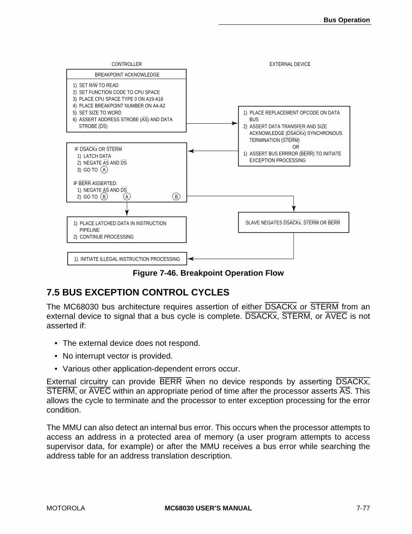
Bus Operation
MOTOROLA MC68030 USER’S MANUAL 7-77
7.5 BUS EXCEPTION CONTROL CYCLESThe MC68030 bus architecture requires assertion of either DSACKx or STERM from anexternal device to signal that a bus cycle is complete. DSACKx, STERM, or AVEC is notasserted if:
• The external device does not respond.
• No interrupt vector is provided.
• Various other application-dependent errors occur.
External circuitry can provide BERR when no device responds by asserting DSACKx,STERM, or AVEC within an appropriate period of time after the processor asserts AS. Thisallows the cycle to terminate and the processor to enter exception processing for the errorcondition.
The MMU can also detect an internal bus error. This occurs when the processor attempts toaccess an address in a protected area of memory (a user program attempts to accesssupervisor data, for example) or after the MMU receives a bus error while searching theaddress table for an address translation description.
Figure 7-46. Breakpoint Operation Flow
1) PLACE REPLACEMENT OPCODE ON DATA BUS2) ASSERT DATA TRANSFER AND SIZE ACKNOWLEDGE (DSACKx) SYNCHRONOUS TERMINATION (STERM) OR1) ASSERT BUS ERRROR (BERR) TO INITIATE EXCEPTION PROCESSING
CONTROLLER
1) SET R/W TO READ2) SET FUNCTION CODE TO CPU SPACE3) PLACE CPU SPACE TYPE 0 ON A19-A164) PLACE BREAKPOINT NUMBER ON A4-A25) SET SIZE TO WORD6) ASSERT ADDRESS STROBE (AS) AND DATA STROBE (DS)
BREAKPOINT ACKNOWLEDGE
1) PLACE LATCHED DATA IN INSTRUCTION PIPELINE2) CONTINUE PROCESSING
1) INITIATE ILLEGAL INSTRUCTION PROCESSING
SLAVE NEGATES DSACKx, STERM OR BERR
EXTERNAL DEVICE
IF DSACKx OR STERM 1) LATCH DATA 2) NEGATE AS AND DS 3) GO TO A
IF BERR ASSERTED: 1) NEGATE AS AND DS 2) GO TO B A B
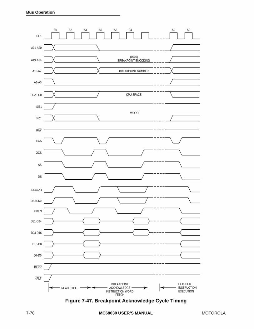
Bus Operation
7-78 MC68030 USER’S MANUAL MOTOROLA
Figure 7-47. Breakpoint Acknowledge Cycle Timing
BREAKPOINTACKNOWLEDGE
INSTRUCTION WORDFETCH
READ CYCLE
CLK
A31-A20
A19-A16
A15-A2
FC2-FC0
SIZ1
R/W
ECS
OCS
AS
DSACK0
D31-D24
D23-D16
SIZ0
DSACK1
S0 S2 S4 S0 S2 S4 S0 S2
D7-D0
D15-D8
BREAKPOINT NUMBER
WORD
FETCHEDINSTRUCTIONEXECUTION
(0000)BREAKPOINT ENCODING
A1-A0
HALT
BERR
CPU SPACE
DS
DBEN
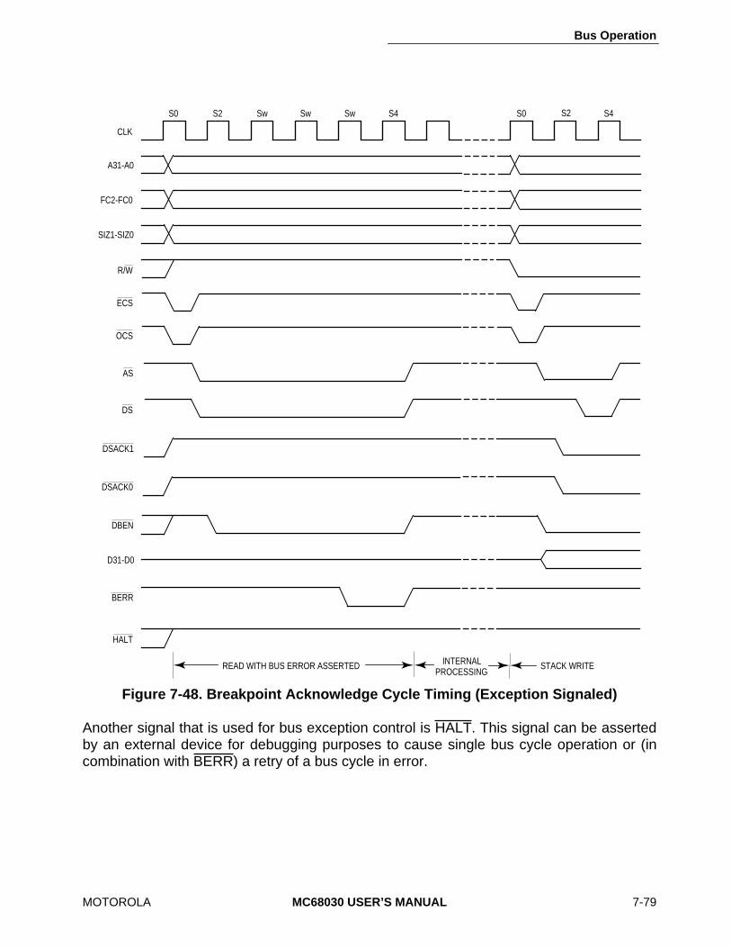
Bus Operation
MOTOROLA MC68030 USER’S MANUAL 7-79
Another signal that is used for bus exception control is HALT. This signal can be assertedby an external device for debugging purposes to cause single bus cycle operation or (incombination with BERR) a retry of a bus cycle in error.
Figure 7-48. Breakpoint Acknowledge Cycle Timing (Exception Signaled)
CLK
A31-A0
FC2-FC0
R/W
ECS
OCS
AS
DS
DSACK0
DBEN
SIZ1-SIZ0
DSACK1
S0 S2 S4 S0 S2
HALT
SwSw Sw S4
D31-D0
BERR
READ WITH BUS ERROR ASSERTED INTERNALPROCESSING
STACK WRITE
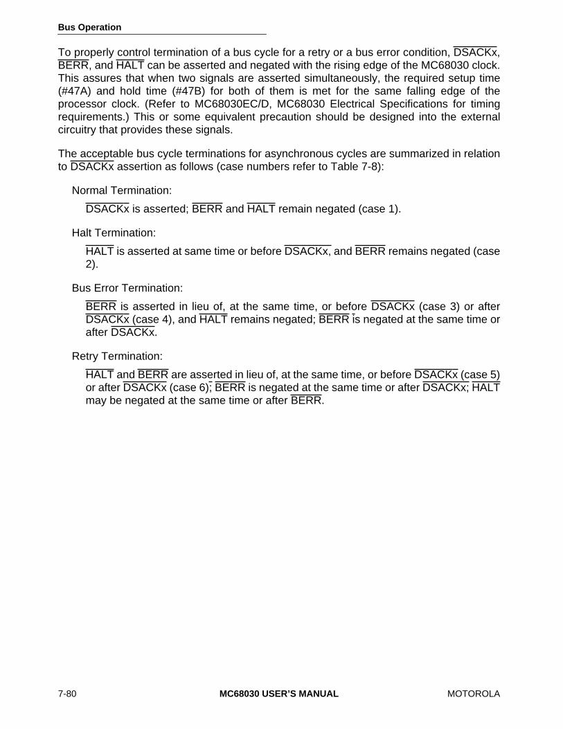
Bus Operation
7-80 MC68030 USER’S MANUAL MOTOROLA
To properly control termination of a bus cycle for a retry or a bus error condition, DSACKx,BERR, and HALT can be asserted and negated with the rising edge of the MC68030 clock.This assures that when two signals are asserted simultaneously, the required setup time(#47A) and hold time (#47B) for both of them is met for the same falling edge of theprocessor clock. (Refer to MC68030EC/D, MC68030 Electrical Specifications for timingrequirements.) This or some equivalent precaution should be designed into the externalcircuitry that provides these signals.
The acceptable bus cycle terminations for asynchronous cycles are summarized in relationto DSACKx assertion as follows (case numbers refer to Table 7-8):
Normal Termination:
DSACKx is asserted; BERR and HALT remain negated (case 1).
Halt Termination:
HALT is asserted at same time or before DSACKx, and BERR remains negated (case2).
Bus Error Termination:
BERR is asserted in lieu of, at the same time, or before DSACKx (case 3) or afterDSACKx (case 4), and HALT remains negated; BERR is negated at the same time orafter DSACKx.
Retry Termination:
HALT and BERR are asserted in lieu of, at the same time, or before DSACKx (case 5)or after DSACKx (case 6); BERR is negated at the same time or after DSACKx; HALTmay be negated at the same time or after BERR.
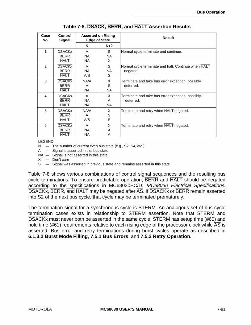
Bus Operation
MOTOROLA MC68030 USER’S MANUAL 7-81
LEGEND:N — The number of current even bus state (e.g., S2, S4, etc.)A — Signal is asserted in this bus stateNA — Signal is not asserted in this stateX — Don't careS — Signal was asserted in previous state and remains asserted in this state
Table 7-8 shows various combinations of control signal sequences and the resulting buscycle terminations. To ensure predictable operation, BERR and HALT should be negatedaccording to the specifications in MC68030EC/D, MC68030 Electrical Specifications.DSACKx, BERR, and HALT may be negated after AS. If DSACKx or BERR remain assertedinto S2 of the next bus cycle, that cycle may be terminated prematurely.
The termination signal for a synchronous cycle is STERM. An analogous set of bus cycletermination cases exists in relationship to STERM assertion. Note that STERM andDSACKx must never both be asserted in the same cycle. STERM has setup time (#60) andhold time (#61) requirements relative to each rising edge of the processor clock while AS isasserted. Bus error and retry terminations during burst cycles operate as described in6.1.3.2 Burst Mode Filling, 7.5.1 Bus Errors, and 7.5.2 Retry Operation.
Table 7-8. DSACK, BERR, and HALT Assertion Results
Case No.
Control Signal
Asserted on RisingEdge of State
Result
N N+2
1 DSACKxBERRHALT
ANANA
SNAX
Normal cycle terminate and continue.
2 DSACKxBERRHALT
ANAA/S
SNAS
Normal cycle terminate and halt. Continue when HALT negated.
3 DSACKxBERRHALT
NA/AA
NA
XS
NA
Terminate and take bus error exception, possibly deferred.
4 DSACKxBERRHALT
ANANA
XA
NA
Terminate and take bus error exception, possibly deferred.
5 DSACKxBERRHALT
NA/AA
A/S
XSS
Terminate and retry when HALT negated.
6 DSACKxBERRHALT
ANANA
XAA
Terminate and retry when HALT negated.
Bus Operation
7-82 MC68030 USER’S MANUAL MOTOROLA
For STERM, the bus cycle terminations are summarized as follows (case numbers refer toTable 7-9):
Normal Termination:
STERM is asserted; BERR and HALT remain negated (case 1).
Halt Termination:
HALT is asserted before STERM, and BERR remains negated (case 2).
Bus Error Termination:
BERR is asserted in lieu of, at the same time, or before STERM (case 3) or afterSTERM (case 4), and HALT remains negated; BERR is negated at the same time or after STERM.
Retry Termination:
HALT and BERR are asserted in lieu of, at the same time, or before STERM (case 5)or after STERM (case 6); BERR is negated at the same time or after STERM; HALTmay be negated at the same time or after BERR.
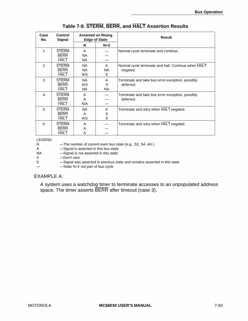
Bus Operation
MOTOROLA MC68030 USER’S MANUAL 7-83
LEGEND:N —The number of current even bus state (e.g., S2, S4, etc.)A —Signal is asserted in this bus stateNA —Signal is not asserted in this stateX —Don't careS —Signal was asserted in previous state and remains asserted in this state— —State N+2 not part of bus cycle
EXAMPLE A:
A system uses a watchdog timer to terminate accesses to an unpopulated address space. The timer asserts BERR after timeout (case 3).
Table 7-9. STERM, BERR, and HALT Assertion Results
Case No.
Control Signal
Asserted on RisingEdge of State
Result
N N+2
1 STERMBERRHALT
ANANA
———
Normal cycle terminate and continue.
2 STERMBERRHALT
NANAA/S
ANAS
Normal cycle terminate and halt. Continue when HALT negated.
3 STERMBERRHALT
NAA/SNA
AS
NA
Terminate and take bus error exception, possiblydeferred.
4 STERMBERRHALT
AA
N/A
———
Terminate and take bus error exception, possibly deferred.
5 STERMBERRHALT
NAA
A/S
ASS
Terminate and retry when HALT negated.
6 STERMBERRHALT
AAA
———
Terminate and retry when HALT negated.

Bus Operation
7-84 MC68030 USER’S MANUAL MOTOROLA
EXAMPLE B:
A system uses error detection and correction on RAM contents. The designer may:
1. Delay DSACKx until data is verified; assert BERR and HALT simultaneously to indi-cate to the processor to automatically retry the error cycle (case 5) or, if data is valid, assert DSACKx (case 1).
2. Delay DSACKx until data is verified and assert BERR with or without DSACKx if data is in error (case 3). This initiates exception processing for software handling of the condition.
3. Return DSACKx prior to data verification. If data is invalid, BERR is asserted on the next clock cycle (case 4). This initiates exception processing for software handling of the condition.
4. Return DSACKx prior to data verification; if data is invalid, assert BERR and HALT on the next clock cycle (case 6). The memory controller can then correct the RAM prior to or during the automatic retry.
7.5.1 Bus ErrorsThe bus error signal can be used to abort the bus cycle and the instruction being executed.BERR takes precedence over DSACKx or STERM provided it meets the timing constraintsdescribed in MC68030EC/D, MC68030 Electrical Specifications. If BERR does not meetthese constraints, it may cause unpredictable operation of the MC68030. If BERR remainsasserted into the next bus cycle, it may cause incorrect operation of that cycle.
When the bus error signal is issued to terminate a bus cycle, the MC68030 may enterexception processing immediately following the bus cycle, or it may defer processing theexception. The instruction prefetch mechanism requests instruction words from the buscontroller and the instruction cache before it is ready to execute them. If a bus error occurson an instruction fetch, the processor does not take the exception until it attempts to use thatinstruction word. Should an intervening instruction cause a branch or should a task switchoccur, the bus error exception does not occur.

Bus Operation
MOTOROLA MC68030 USER’S MANUAL 7-85
The bus error signal is recognized during a bus cycle in any of the following cases:
• DSACKx (or STERM) and HALT are negated and BERR is asserted.
• HALT and BERR are negated and DSACKx is asserted. BERR is then asserted within one clock cycle (HALT remains negated).
• BERR is asserted and recognized on the next falling clock edge following the rising clock edge on which STERM is asserted and recognized (HALT remains negated).
When the processor recognizes a bus error condition, it terminates the current bus cycle inthe normal way. Figure 7-49 shows the timing of a bus error for the case in which neitherDSACKx nor STERM is asserted. Figure 7-50 shows the timing for a bus error that isasserted after DSACKx. Exceptions are taken in both cases. (Refer to 8.1.2 Bus ErrorException for details of bus error exception processing.) When BERR is asserted during aread cycle that supplies data to either on-chip cache, the data in the cache is marked invalid.However, when a write cycle that writes data into the data cache results in an externallygenerated bus error, the data in the cache is not marked invalid.
In the second case, where BERR is asserted after DSACKx is asserted, BERR must beasserted within specification #48 (refer to MC68030EC/D, MC68030 ElectricalSpecifications) for purely asynchronous operation, or it must be asserted and remain stableduring the sample window, defined by specifications #27A and #47B, around the next fallingedge of the clock after DSACKx is recognized. If BERR is not stable at this time, theprocessor may exhibit erratic behavior. BERR has priority over DSACKx. In this case, datamay be present on the bus, but may not be valid. This sequence may be used by systemsthat have memory error detection and correction logic and by external cache memories.
The assertion of BERR described in the third case (recognized after STERM) hasrequirements similar to those described in the preceding paragraph. BERR must be stablethroughout the sample window for the next falling edge of the clock, as defined byspecifications #27A and #28A. Figure 7-51 shows the timing for this case.
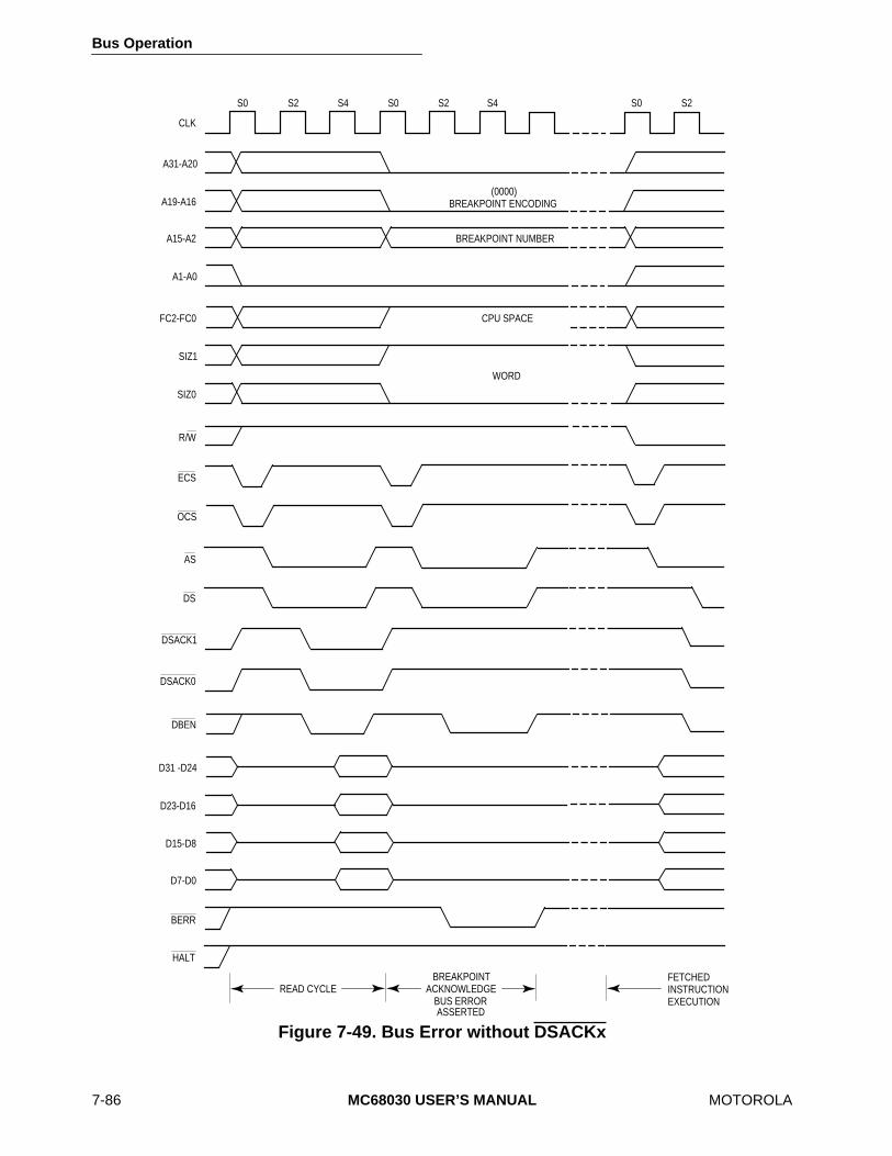
Bus Operation
7-86 MC68030 USER’S MANUAL MOTOROLA
Figure 7-49. Bus Error without DSACKx
BREAKPOINTACKNOWLEDGE
BUS ERRORASSERTED
READ CYCLE
CLK
A31-A20
A19-A16
A15-A2
FC2-FC0
SIZ1
R/W
ECS
OCS
AS
DS
DSACK0
DBEN
D23-D16
SIZ0
DSACK1
S0 S2 S4 S0 S2 S4 S0 S2
D7-D0
D15-D8
BREAKPOINT NUMBER
WORD
FETCHEDINSTRUCTIONEXECUTION
(0000)BREAKPOINT ENCODING
A1-A0
HALT
BERR
CPU SPACE
D31 -D24
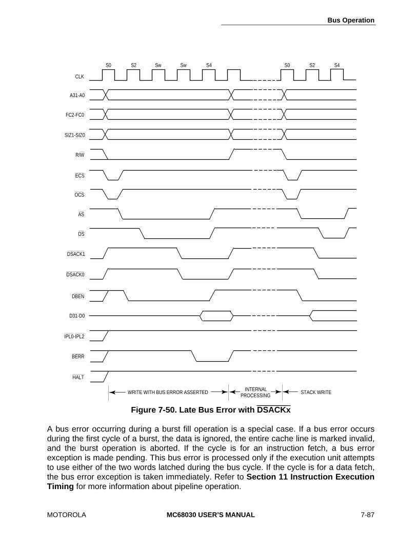
Bus Operation
MOTOROLA MC68030 USER’S MANUAL 7-87
A bus error occurring during a burst fill operation is a special case. If a bus error occursduring the first cycle of a burst, the data is ignored, the entire cache line is marked invalid,and the burst operation is aborted. If the cycle is for an instruction fetch, a bus errorexception is made pending. This bus error is processed only if the execution unit attemptsto use either of the two words latched during the bus cycle. If the cycle is for a data fetch,the bus error exception is taken immediately. Refer to Section 11 Instruction ExecutionTiming for more information about pipeline operation.
Figure 7-50. Late Bus Error with DSACKx
CLK
A31-A0
FC2-FC0
R/W
ECS
OCS
AS
DS
DSACK0
DBEN
D31-D0
IPL0-IPL2
DSACK1
S0 S2 Sw S4 S0 S2Sw S4
SIZ1-SIZ0
BERR
HALT
WRITE WITH BUS ERROR ASSERTED INTERNALPROCESSING
STACK WRITE

Bus Operation
7-88 MC68030 USER’S MANUAL MOTOROLA
When a bus error occurs after the burst mode has been entered (that is, on the secondaccess or later), the processor terminates the burst operation, and the cache entrycorresponding to that cycle is marked invalid, but the processor does not take an exception(see Figure 7-52). If the second cycle is for a portion of a misaligned operand fetch, theprocessor runs another read cycle for the second portion with CBREQ negated, as shownin Figure 7-53. If BERR is asserted again, the MC68030 then takes an exception. TheMC68030 supports late bus errors during a burst fill operation; the timing is the same relativeto STERM and the clock as for a late bus error in a normal synchronous cycle.
Figure 7-51. Late Bus Error with STERM — Exception Taken
AS
CLK
A31-A0
FC2-FC0
SIZ1–SIZ0
S0 S2 S3 S0 S2SwSwSw Sw
R/W
ECS
OCS
DS
STERM
DBEN
BERR
D31-D0
HALT
WRITE WITH BUS ERROR ASSERTED INTERNALPROCESSING
STACK WRITE
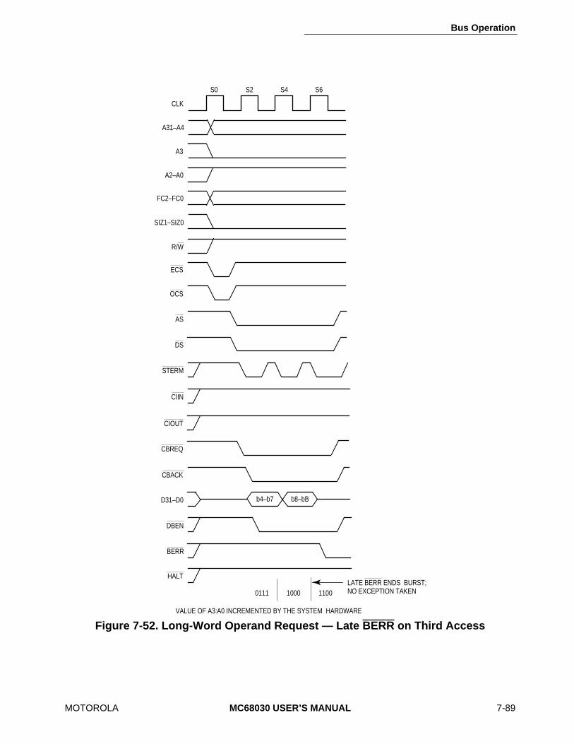
Bus Operation
MOTOROLA MC68030 USER’S MANUAL 7-89
Figure 7-52. Long-Word Operand Request — Late BERR on Third Access
CLK
A31–A4
A3
A2–A0
FC2–FC0
SIZ1–SIZ0
R/W
S0 S2 S4 S6
ECS
OCS
AS
DS
b4–b7 b8–bB
0111 1000 1100
STERM
CIIN
CIOUT
CBREQ
CBACK
D31–D0
DBEN
BERR
HALTLATE BERR ENDS BURST;NO EXCEPTION TAKEN
VALUE OF A3:A0 INCREMENTED BY THE SYSTEM HARDWARE
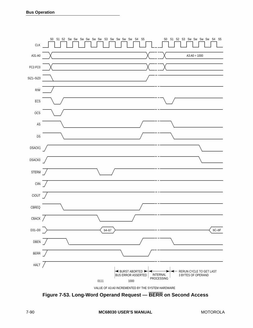
Bus Operation
7-90 MC68030 USER’S MANUAL MOTOROLA
Figure 7-53. Long-Word Operand Request — BERR on Second Access
FC2-FC0
R/W
ECS
OCS
CLK
S0 S2 SwS1 Sw Sw Sw SwS4 S5 Sw Sw
AS
DS
STERM
CBREQ
CBACK
D31–D0
DBEN
b4–b7 bC–bF
SwSw SwSw S3
SIZ1–SIZ0
CIIN
CIOUT
Sw Sw S0 S1 S2 S3 S4 S5Sw
A31-A0 A3:A0 = 1000
DSACK1
DSACK0
BERR
HALT
BURST ABORTEDBUS ERROR ASSERTED INTERNAL
PROCESSING
RERUN CYCLE TO GET LAST3 BYTES OF OPERAND
0111 1000
VALUE OF A3:A0 INCREMENTED BY THE SYSTEM HARDWARE

Bus Operation
MOTOROLA MC68030 USER’S MANUAL 7-91
7.5.2 Retry OperationWhen the BERR and HALT signals are both asserted by an external device during a buscycle, the processor enters the retry sequence. A delayed retry, similar to the delayed buserror signal described previously, can also occur, both for synchronous and asynchronouscycles.
The processor terminates the bus cycle, places the control signals in their inactive state, anddoes not begin another bus cycle until the HALT signal is negated by external logic. After asynchronization delay, the processor retries the previous cycle using the same accessinformation (address, function code, size, etc.) The BERR signal should be negated beforeS2 of the read cycle to ensure correct operation of the retried cycle. Figure 7-54 shows aretry operation of an asynchronous cycle, and Figure 7-55 shows a retry operation of asynchronous cycle.
The processor retries any read or write cycle of a read-modify-write operation separately;RMC remains asserted during the entire retry sequence.
On the initial access of a burst operation, a retry (indicated by the assertion of BERR andHALT) causes the processor to retry the bus cycle and assert CBREQ again. Figure 7-56shows a late retry operation that causes an initial burst operation to be repeated. However,signaling a retry with simultaneous BERR and HALT during the second, third, or fourth cycleof a burst operation does not cause a retry operation, even if the requested operand ismisaligned. Assertion of BERR and HALT during a subsequent cycle of a burst operationcauses independent BERR and HALT operations. The external bus activity remains halteduntil HALT is negated and the processor acts as previously described for the bus errorduring a burst operation.
Asserting BR along with BERR and HALT provides a relinquish and retry operation. TheMC68030 does not relinquish the bus during a read-modify-write operation, except duringthe first read cycle. Any device that requires the processor to give up the bus and retry a buscycle during a read-modify-write cycle must either assert BERR and BR only (HALT mustnot be included) or use the single wire arbitration method discussed in 7.7.4 BusArbitration Control. The bus error handler software should examine the read-modify-writebit in the special status word (refer to 8.2.1 Special Status Word (SSW)) and take theappropriate action to resolve this type of fault when it occurs.
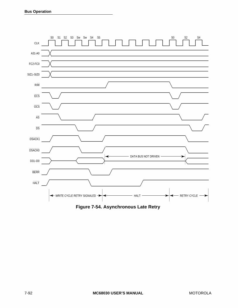
Bus Operation
7-92 MC68030 USER’S MANUAL MOTOROLA
Figure 7-54. Asynchronous Late Retry
A31-A0
FC2-FC0
R/W
ECS
OCS
CLK
S0 S2 SwS1
AS
DS
D31–D0
Sw
SIZ1–SIZ0
S3 S4 S5 S0 S2 S4
DSACK1
DSACK0
DATA BUS NOT DRIVEN
BERR
HALT
WRITE CYCLE RETRY SIGNALED HALT RETRY CYCLE

Bus Operation
7-93 MC68030 USER’S MANUAL MOTOROLA
7.5.3 Halt OperationWhen HALT is asserted and BERR is not asserted, the MC68030 halts external bus activityat the next bus cycle boundary. HALT by itself does not terminate a bus cycle. Negating andreasserting HALT in accordance with the correct timing requirements provides a single-step(bus cycle to bus cycle) operation. The HALT signal affects external bus cycles only; thus,a program that resides in the instruction cache and performs no data writes (or reads thatmiss in the data cache) may continue executing, unaffected by the HALT signal.
Figure 7-55. Synchronous Late Retry
A31-A0
FC2-FC0
R/W
ECS
OCS
CLK
S0 S2S1
AS
DS
STERM
SIZ1–SIZ0
S3 S0 S1 S2 S3
D31–D0
BERR
HALT
READ CYCLERETRY SIGNALED
HALT RETRY CYCLE

Bus Operation
7-94 MC68030 USER’S MANUAL MOTOROLA
The single-cycle mode allows the user to proceed through (and debug) external processoroperations, one bus cycle at a time. Figure 7-57 shows the timing requirements for a single-cycle operation. Since the occurrence of a bus error while HALT is asserted causes a retryoperation, the user must anticipate retry cycles while debugging in the single-cycle mode.The single-step operation and the software trace capability allow the system debugger totrace single bus cycles, single instructions, or changes in program flow. These processorcapabilities, along with a software debugging package, give complete debugging flexibility.
Figure 7-56. Late Retry Operation for a Burst
A31-A0
FC2-FC0
R/W
ECS
OCS
CLK
S0 S2S1
AS
DS
STERM
SIZ1–SIZ0
S3 S0 S1 S2 S3
D31–D0
BERR
HALT
S4
CIIN
CIOUT
CBREQ
CBACK
READ HALT RETRY
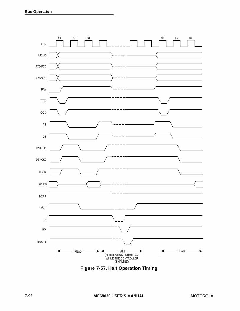
Bus Operation
7-95 MC68030 USER’S MANUAL MOTOROLA
Figure 7-57. Halt Operation Timing
CLK
A31-A0
FC2-FC0
R/W
ECS
OCS
AS
DS
DSACK0
DBEN
DSACK1
S0 S2 S0
BERR
HALT
S4 S2
SIZ1/SIZ0
S4
D31-D0
BR
BG
BGACK
READ HALT(ARBITRATION PERMITTEDWHILE THE CONTROLLER
IS HALTED)
READ
Bus Operation
7-96 MC68030 USER’S MANUAL MOTOROLA
When the processor completes a bus cycle with the HALT signal asserted, the data bus isplaced in the high-impedance state, and bus control signals are driven inactive (not high-impedance state); the address, function code, size, and read/write signals remain in thesame state. The halt operation has no effect on bus arbitration (refer to 7.7 BusArbitration). When bus arbitration occurs while the MC68030 is halted, the address andcontrol signals are also placed in the high-impedance state. Once bus mastership isreturned to the MC68030, if HALT is still asserted, the address, function code, size, andread/write signals are again driven to their previous states. The processor does not serviceinterrupt requests while it is halted, but it may assert the IPEND signal as appropriate.
7.5.4 Double Bus FaultWhen a bus error or an address error occurs during the exception processing sequence fora previous bus error, a previous address error, or a reset exception, the bus or address errorcauses a double bus fault. For example, the processor attempts to stack several wordscontaining information about the state of the machine while processing a bus errorexception. If a bus error exception occurs during the stacking operation, the second error isconsidered a double bus fault. Only an external reset operation can restart a haltedprocessor. However, bus arbitration can still occur (refer to 7.7 Bus Arbitration).
The MC68030 indicates that a double bus fault condition has occurred by continuouslyasserting the STATUS signal until the processor is reset. The processor asserts STATUSfor one, two, or three clock periods to signal other microsequencer status indications. Referto Section 12 Applications Information for a description of the interpretation of theSTATUS signal.
A second bus error or address error that occurs after exception processing has completed(during the execution of the exception handler routine or later) does not cause a double busfault. A bus cycle that is retried does not constitute a bus error or contribute to a double busfault. The processor continues to retry the same bus cycle as long as the external hardwarerequests it.

Bus Operation
7-97 MC68030 USER’S MANUAL MOTOROLA
7.6 BUS SYNCHRONIZATIONThe MC68030 overlaps instruction execution; that is, during bus activity for one instruction,instructions that do not use the external bus can be executed. Due to the independentoperation of the on-chip caches relative to the operation of the bus controller, manysubsequent instructions can be executed, resulting in seemingly nonsequential instructionexecution. When this is not desired and the system depends on sequential executionfollowing bus activity, the NOP instruction can be used. The NOP instruction forcesinstruction and bus synchronization in that it freezes instruction execution until all pendingbus cycles have completed.
An example of the use of the NOP instruction for this purpose is the case of a write operationof control information to an external register, where the external hardware attempts tocontrol program execution based on the data that is written with the conditional assertion ofBERR. If the data cache is enabled and the write cycle results in a hit in the data cache, thecache is updated. That data, in turn, may be used in a subsequent instruction before theexternal write cycle completes. Since the MC68030 cannot process the bus error until theend of the bus cycle, the external hardware has not successfully interrupted programexecution. To prevent a subsequent instruction from executing until the external cyclecompletes, a NOP instruction can be inserted after the instruction causing the write. In thiscase, bus error exception processing proceeds immediately after the write beforesubsequent instructions are executed. This is an irregular situation, and the use of the NOPinstruction for this purpose is not required by most systems.
Note that even in a system with error detection/correction circuitry, the NOP is not requiredfor this synchronization. Since the MMU always checks the validity of write cycles beforethey proceed to the data cache and are executed externally, the MC68030 is guaranteed towrite correct data to the cache. Thus, there is no danger in subsequent instructions usingerroneous data from the cache before an external bus error signals an error.
A bus synchronization example is given in Figure 7-58.
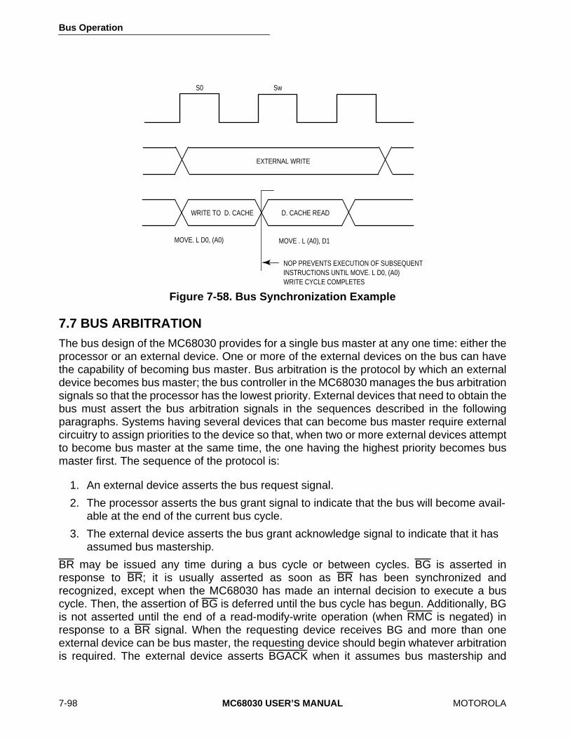
Bus Operation
7-98 MC68030 USER’S MANUAL MOTOROLA
7.7 BUS ARBITRATIONThe bus design of the MC68030 provides for a single bus master at any one time: either theprocessor or an external device. One or more of the external devices on the bus can havethe capability of becoming bus master. Bus arbitration is the protocol by which an externaldevice becomes bus master; the bus controller in the MC68030 manages the bus arbitrationsignals so that the processor has the lowest priority. External devices that need to obtain thebus must assert the bus arbitration signals in the sequences described in the followingparagraphs. Systems having several devices that can become bus master require externalcircuitry to assign priorities to the device so that, when two or more external devices attemptto become bus master at the same time, the one having the highest priority becomes busmaster first. The sequence of the protocol is:
1. An external device asserts the bus request signal.
2. The processor asserts the bus grant signal to indicate that the bus will become avail-able at the end of the current bus cycle.
3. The external device asserts the bus grant acknowledge signal to indicate that it has assumed bus mastership.
BR may be issued any time during a bus cycle or between cycles. BG is asserted inresponse to BR; it is usually asserted as soon as BR has been synchronized andrecognized, except when the MC68030 has made an internal decision to execute a buscycle. Then, the assertion of BG is deferred until the bus cycle has begun. Additionally, BGis not asserted until the end of a read-modify-write operation (when RMC is negated) inresponse to a BR signal. When the requesting device receives BG and more than oneexternal device can be bus master, the requesting device should begin whatever arbitrationis required. The external device asserts BGACK when it assumes bus mastership and
Figure 7-58. Bus Synchronization Example
S0 Sw
EXTERNAL WRITE
WRITE TO D. CACHE D. CACHE READ
MOVE. L D0, (A0)
NOP PREVENTS EXECUTION OF SUBSEQUENTINSTRUCTIONS UNTIL MOVE. L D0, (A0)WRITE CYCLE COMPLETES
MOVE . L (A0), D1

Bus Operation
7-99 MC68030 USER’S MANUAL MOTOROLA
maintains BGACK during the entire bus cycle (or cycles) for which it is bus master. Thefollowing conditions must be met for an external device to assume mastership of the busthrough the normal bus arbitration procedure:
• It must have received BG through the arbitration process.
• AS must be negated, indicating that no bus cycle is in progress, and the external device must ensure that all appropriate processor signals have been placed in the high-imped-ance state (by observing specification #7 in MC68030EC/D, MC68030 Electrical Spec-ifications).
• The termination signal (DSACKx or STERM) for the most recent cycle must have be-come inactive, indicating that external devices are off the bus (optional, refer to 7.7.3 Bus Grant Acknowledge).
• BGACK must be inactive, indicating that no other bus master has claimed ownership of the bus.
Figure 7-59 is a flowchart showing the detail involved in bus arbitration for a single device.Figure 7-60 is a timing diagram for the same operation. This technique allows processing ofbus requests during data transfer cycles.
The timing diagram shows that BR is negated at the time that BGACK is asserted. This typeof operation applies to a system consisting of the processor and one device capable of busmastership. In a system having a number of devices capable of bus mastership, the busrequest line from each device can be wire-ORed to the processor. In such a system, morethan one bus request can be asserted simultaneously.
The timing diagram in Figure 7-60 shows that BG is negated a few clock cycles after thetransition of the BGACK signal. However, if bus requests are still pending after the negationof BG, the processor asserts another BG within a few clock cycles after it was negated. Thisadditional assertion of BG allows external arbitration circuitry to select the next bus masterbefore the current bus master has finished with the bus. The following paragraphs provideadditional information about the three steps in the arbitration process.
Bus arbitration requests are recognized during normal processing, RESET assertion, HALTassertion, and even when the processor has halted due to a double bus fault.
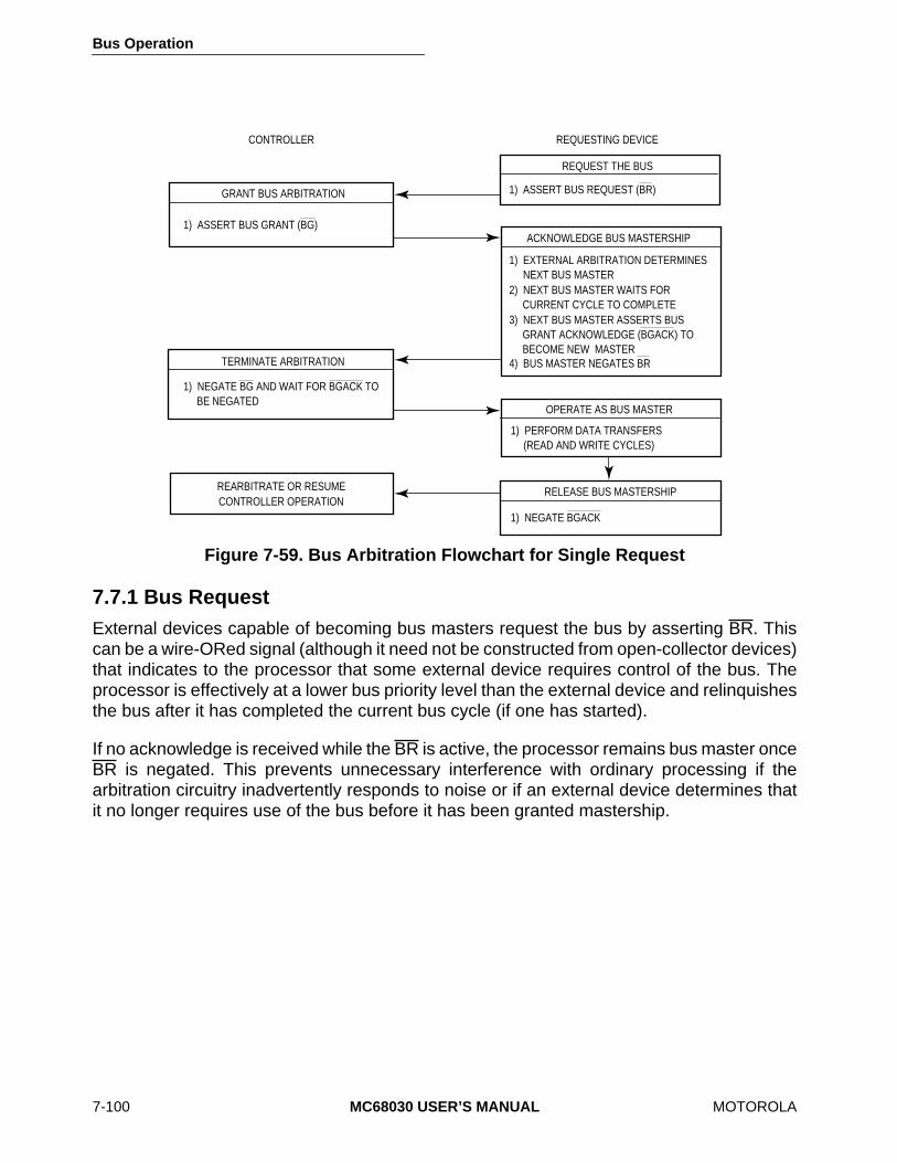
Bus Operation
7-100 MC68030 USER’S MANUAL MOTOROLA
7.7.1 Bus RequestExternal devices capable of becoming bus masters request the bus by asserting BR. Thiscan be a wire-ORed signal (although it need not be constructed from open-collector devices)that indicates to the processor that some external device requires control of the bus. Theprocessor is effectively at a lower bus priority level than the external device and relinquishesthe bus after it has completed the current bus cycle (if one has started).
If no acknowledge is received while the BR is active, the processor remains bus master onceBR is negated. This prevents unnecessary interference with ordinary processing if thearbitration circuitry inadvertently responds to noise or if an external device determines thatit no longer requires use of the bus before it has been granted mastership.
Figure 7-59. Bus Arbitration Flowchart for Single Request
1) ASSERT BUS GRANT (BG)
GRANT BUS ARBITRATION
TERMINATE ARBITRATION
1) NEGATE BG AND WAIT FOR BGACK TO BE NEGATED
REARBITRATE OR RESUMECONTROLLER OPERATION
REQUEST THE BUS
1) ASSERT BUS REQUEST (BR)
REQUESTING DEVICECONTROLLER
ACKNOWLEDGE BUS MASTERSHIP
1) EXTERNAL ARBITRATION DETERMINES NEXT BUS MASTER2) NEXT BUS MASTER WAITS FOR CURRENT CYCLE TO COMPLETE3) NEXT BUS MASTER ASSERTS BUS GRANT ACKNOWLEDGE (BGACK) TO BECOME NEW MASTER4) BUS MASTER NEGATES BR
OPERATE AS BUS MASTER
RELEASE BUS MASTERSHIP
1) PERFORM DATA TRANSFERS (READ AND WRITE CYCLES)
1) NEGATE BGACK

Bus Operation
7-101 MC68030 USER’S MANUAL MOTOROLA
7.7.2 Bus GrantThe processor asserts BG as soon as possible after receipt of BR. This is immediatelyfollowing internal synchronization except during a read-modify-write cycle or following aninternal decision to execute a bus cycle. During a read-modify-write cycle, the processordoes not assert BG until the entire operation has completed. RMC is asserted to indicate
Figure 7-60. Bus Arbitration Operation Timing
A31-A0
FC2-FC0
ECS
OCS
AS
DS
DSACK1
CLK
S0 S4 S0
SIZ1-SIZ0
R/W
DSACK0
DBEN
S2 S2
BGACK
BG
BR
D31-D0
CONTROLLER DMA DEVICE CONTROLLER
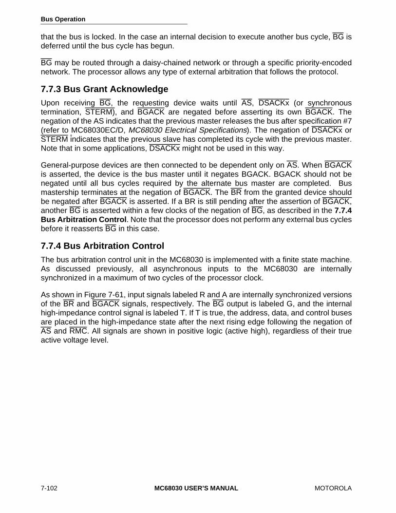
Bus Operation
7-102 MC68030 USER’S MANUAL MOTOROLA
that the bus is locked. In the case an internal decision to execute another bus cycle, BG isdeferred until the bus cycle has begun.
BG may be routed through a daisy-chained network or through a specific priority-encodednetwork. The processor allows any type of external arbitration that follows the protocol.
7.7.3 Bus Grant AcknowledgeUpon receiving BG, the requesting device waits until AS, DSACKx (or synchronoustermination, STERM), and BGACK are negated before asserting its own BGACK. Thenegation of the AS indicates that the previous master releases the bus after specification #7(refer to MC68030EC/D, MC68030 Electrical Specifications). The negation of DSACKx orSTERM indicates that the previous slave has completed its cycle with the previous master.Note that in some applications, DSACKx might not be used in this way.
General-purpose devices are then connected to be dependent only on AS. When BGACKis asserted, the device is the bus master until it negates BGACK. BGACK should not benegated until all bus cycles required by the alternate bus master are completed. Busmastership terminates at the negation of BGACK. The BR from the granted device shouldbe negated after BGACK is asserted. If a BR is still pending after the assertion of BGACK,another BG is asserted within a few clocks of the negation of BG, as described in the 7.7.4Bus Arbitration Control. Note that the processor does not perform any external bus cyclesbefore it reasserts BG in this case.
7.7.4 Bus Arbitration ControlThe bus arbitration control unit in the MC68030 is implemented with a finite state machine.As discussed previously, all asynchronous inputs to the MC68030 are internallysynchronized in a maximum of two cycles of the processor clock.
As shown in Figure 7-61, input signals labeled R and A are internally synchronized versionsof the BR and BGACK signals, respectively. The BG output is labeled G, and the internalhigh-impedance control signal is labeled T. If T is true, the address, data, and control busesare placed in the high-impedance state after the next rising edge following the negation ofAS and RMC. All signals are shown in positive logic (active high), regardless of their trueactive voltage level.
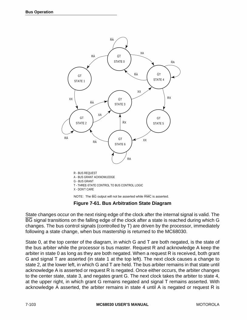
Bus Operation
7-103 MC68030 USER’S MANUAL MOTOROLA
State changes occur on the next rising edge of the clock after the internal signal is valid. TheBG signal transitions on the falling edge of the clock after a state is reached during which Gchanges. The bus control signals (controlled by T) are driven by the processor, immediatelyfollowing a state change, when bus mastership is returned to the MC68030.
State 0, at the top center of the diagram, in which G and T are both negated, is the state ofthe bus arbiter while the processor is bus master. Request R and acknowledge A keep thearbiter in state 0 as long as they are both negated. When a request R is received, both grantG and signal T are asserted (in state 1 at the top left). The next clock causes a change tostate 2, at the lower left, in which G and T are held. The bus arbiter remains in that state untilacknowledge A is asserted or request R is negated. Once either occurs, the arbiter changesto the center state, state 3, and negates grant G. The next clock takes the arbiter to state 4,at the upper right, in which grant G remains negated and signal T remains asserted. Withacknowledge A asserted, the arbiter remains in state 4 until A is negated or request R is
Figure 7-61. Bus Arbitration State Diagram
RA
RA
XX
RARA
RA
XX
RX
RA
XA
RA
RX
XA
RA
GT
STATE 1
GT
STATE 0
GT
STATE 4
GT
STATE 5
GT
STATE 6
GT
STATE 2
GT
STATE 3
XX
R - BUS REQUESTA - BUS GRANT ACKNOWLEDGEG - BUS GRANTT - THREE-STATE CONTROL TO BUS CONTROL LOGICX - DON'T CARE
NOTE: The BG output will not be asserted while RMC is asserted.

Bus Operation
7-104 MC68030 USER’S MANUAL MOTOROLA
again asserted. When A is negated, the arbiter returns to the original state, state 0, andnegates signal T. This sequence of states follows the normal sequence of signals forrelinquishing the bus to an external bus master. Other states apply to other possiblesequences of combinations of R and A. As shown by the path from state 0 to state 4, BGACKalone can be used to place the processor's external bus buffers in the high-impedance state,providing single-wire arbitration capability.
The read-modify-write sequence is normally indivisible to support semaphore operationsand multiprocessor synchronization. During this indivisible sequence, the MC68030 assertsthe RMC signal and causes the bus arbitration state machine to ignore bus requests(assertions of BR) that occur after the first read cycle of the read-modify-write sequence bynot issuing bus grants (asserting BG).
In some cases, however, it may be necessary to force the MC68030 to release the busduring an read-modify-write sequence. One way for an alternate bus master to force theMC68030 to release the bus applies only to the first read cycle of an read-modify-writesequence. The MC68030 allows normal bus arbitration during this read cycle; a normalrelinquish and retry operation (asserting BERR, HALT, and BR at the same time) is used.Note that this method applies only to the first read cycle of the read-modify-write sequence,but this method preserves the integrity of the read-modify-write sequence without imposingany constraint on the alternate bus master.
A second method is single-wire arbitration, the timing of which is shown in Figure 7-62. Analternate master forces the MC68030 to release the bus by asserting BGACK and waits forAS to negate before taking the bus. It applies to all bus cycles of a read-modify-writesequence, but can cause system integrity problems if used improperly. The alternate busmaster must guarantee the integrity of the read-modify-write sequence by not altering thecontents of memory locations accessed by the read-modify-write sequence. Note that forthe method to operate properly, AS must be observed to be negated (high) on twoconsecutive clock edges before the alternate bus master takes the bus. Waiting for thiscondition ensures that any current or pending bus activity has completed or has been pre-empted.

Bus Operation
7-105 MC68030 USER’S MANUAL MOTOROLA
A timing diagram of the bus arbitration sequence during a processor bus cycle is shown inFigure 7-60. The bus arbitration sequence while the bus is inactive (i.e., executing internaloperations such as a multiply instruction) is shown in Figure 7-63.
7.8 RESET OPERATIONRESET is a bidirectional signal with which an external device resets the system or theprocessor resets external devices. When power is applied to the system, external circuitryshould assert RESET for a minimum of 520 clocks after VCC is within tolerance. Figure 7-64is a timing diagram of the powerup reset operation, showing the relationships betweenRESET, VCC, and bus signals. The clock signal is required to be stable by the time VCCreaches the minimum operating specification. During the reset period, the entire bus three-states (except for non-three-statable signals, which are driven to their inactive state). OnceRESET negates, all control signals are driven to their inactive state, the data bus is in readmode, and the address bus is driven. After this, the first bus cycle for reset exceptionprocessing begins.
Figure 7-62. Single-Wire Bus Arbitration Timing Diagram
NOTE: The alternate bus master must sample AS high on two consecutive rising edges of the clock (after BGACK isrecognized low) before taking the bus.
16
7
47A
12
TAKE BUS
SEE NOTE
DO NOTTAKE BUS
912
47A
CLK
AS
BGACK
ADDRESS
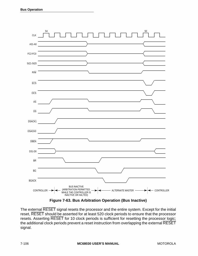
Bus Operation
7-106 MC68030 USER’S MANUAL MOTOROLA
The external RESET signal resets the processor and the entire system. Except for the initialreset, RESET should be asserted for at least 520 clock periods to ensure that the processorresets. Asserting RESET for 10 clock periods is sufficient for resetting the processor logic;the additional clock periods prevent a reset instruction from overlapping the external RESETsignal.
Figure 7-63. Bus Arbitration Operation (Bus Inactive)
A31-A0
FC2-FC0
ECS
OCS
AS
DS
DSACK1
CLK
S4 S0
SIZ1-SIZ0
R/W
DSACK0
DBEN
BGACK
BG
BR
D31-D0
CONTROLLER CONTROLLERALTERNATE MASTER
BUS INACTIVE(ARBITRATION PERMITTEDWHILE THE CONTROLLER IS
INACTIVE OR HALTED)
Bus Operation
7-107 MC68030 USER’S MANUAL MOTOROLA
Resetting the processor causes any bus cycle in progress to terminate as if DSACKx,BERR, or STERM had been asserted. In addition, the processor initializes registersappropriately for a reset exception. Exception processing for a reset operation is describedin 8.1.1 Reset Exception.
When a reset instruction is executed, the processor drives the RESET signal for 512 clockcycles. In this case, the processor resets the external devices of the system, and the internalregisters of the processor are unaffected. The external devices connected to the RESETsignal are reset at the completion of the reset instruction. An external RESET signal that isasserted to the processor during execution of a reset instruction must extend beyond thereset period of the instruction by at least eight clock cycles to reset the processor. Figure 7-65 shows the timing information for the reset instruction.
Figure 7-64. Initial Reset Operation Timing
ISPREAD
STARTS
ALL CONTROL SIGNALSINACTIVE. DATA BUS INREAD MODE. ADDRESS
BUS DRIVEN
ENTIREBUS HIGH
IMPEDANCEBUS STATE UNKNOWN
t = >520 CLOCKS
1<4 CLOCKS
4 CLOCKS
CLK
+5VOLTS
VCC
BUSCYCLES
RESET
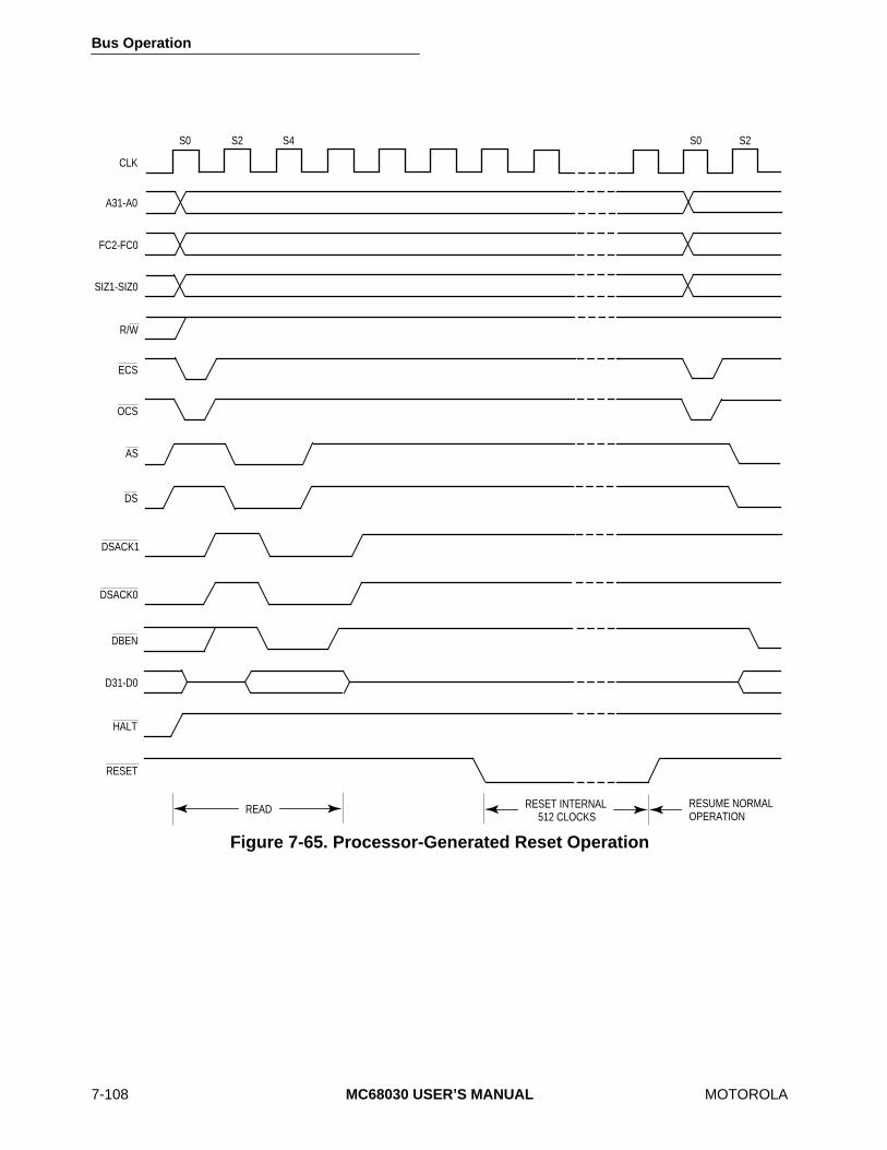
Bus Operation
7-108 MC68030 USER’S MANUAL MOTOROLA
Figure 7-65. Processor-Generated Reset Operation
CLK
A31-A0
FC2-FC0
R/W
ECS
OCS
AS
DS
DSACK0
DBEN
SIZ1-SIZ0
DSACK1
HALT
S0 S2S4
D31-D0
S2S0
RESET
READ RESET INTERNAL512 CLOCKS
RESUME NORMALOPERATION

MOTOROLA
MC68030 USER’S MANUAL
8-1
SECTION 8EXCEPTION PROCESSING
Exception processing is defined as the activities performed by the processor in preparing toexecute a handler routine for any condition that causes an exception. In particular, exceptionprocessing does not include execution of the handler routine itself. An introduction toexception processing, as one of the processing states of the MC68030 processor, was givenin
Section 4 Processing States
. This section describes exception processing in detail,describing the processing for each type of exception. It describes the return from anexception and bus fault recovery. This section also describes the formats of the exceptionstack frames. For details of MMU-related exceptions, refer to
Section 9 MemoryManagement Unit
. For more detail on protocol violation and coprocessor-relatedexceptions, refer to
Section 10 Coprocessor Interface Description
. Also, for more detailon exceptions defined for floating-point coprocessors, refer to the user's manual for theMC68881/MC68882.
8.1 EXCEPTION PROCESSING SEQUENCE
Exception processing occurs in four functional steps. However, all individual bus cyclesassociated with exception processing (vector acquisition, stacking, etc.) are not guaranteedto occur in the order in which they are described in this section. Nonetheless, all addressesand offsets from the stack pointer are guaranteed to be as described.
The first step of exception processing involves the status register. The processor makes aninternal copy of the status register. Then the processor sets the S bit, changing to thesupervisor privilege level. Next, the processor inhibits tracing of the exception handler byclearing the T1 and T0 bits. For the reset and interrupt exceptions, the processor alsoupdates the interrupt priority mask.
In the second step, the processor determines the vector number of the exception. Forinterrupts, the processor performs an interrupt acknowledge cycle (a read from the CPUaddress space type $F; see Figures 7-45 and 7-46) to obtain the vector number. Forcoprocessor-detected exceptions, the vector number is included in the coprocessorexception primitive response.
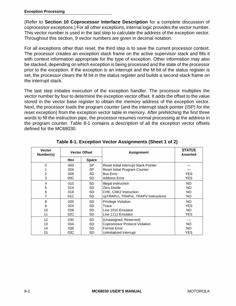
Exception Processing
8-2
MC68030 USER’S MANUAL
MOTOROLA
(Refer to
Section 10 Coprocessor Interface Description
for a complete discussion ofcoprocessor exceptions.) For all other exceptions, internal logic provides the vector number.This vector number is used in the last step to calculate the address of the exception vector.Throughout this section, 9 vector numbers are given in decimal notation.
For all exceptions other than reset, the third step is to save the current processor context.The processor creates an exception stack frame on the active supervisor stack and fills itwith context information appropriate for the type of exception. Other information may alsobe stacked, depending on which exception is being processed and the state of the processorprior to the exception. If the exception is an interrupt and the M bit of the status register isset, the processor clears the M bit in the status register and builds a second stack frame onthe interrupt stack.
The last step initiates execution of the exception handler. The processor multiplies thevector number by four to determine the exception vector offset. It adds the offset to the valuestored in the vector base register to obtain the memory address of the exception vector.Next, the processor loads the program counter (and the interrupt stack pointer (ISP) for thereset exception) from the exception vector table in memory. After prefetching the first threewords to fill the instruction pipe, the processor resumes normal processing at the address inthe program counter. Table 8-1 contains a description of all the exception vector offsetsdefined for the MC68030.
Table 8-1. Exception Vector Assignments (Sheet 1 of 2)
Vector Number(s)
Vector Offset AssignmentSTATUS Asserted
Hex Space
0123
00000400800C
SPSPSDSD
Reset Initial Interrupt Stack PointerReset Initial Program CounterBus ErrorAddress Error
——
YESYES
4567
01001401801C
SDSDSDSD
Illegal InstructionZero DivideCHK, CHK2 InstructioncpTRAPcc, TRAPcc, TRAPV Instructions
NONONONO
891011
02002402802C
SDSDSDSD
Privilege ViolationTraceLine 1010 EmulatorLine 1111 Emulator
NOYESNOYES
12131415
03003403803C
SDSDSDSD
(Unassigned, Reserved)Coprocessor Protocol ViolationFormat ErrorUninitialized Interrupt
—NONOYES
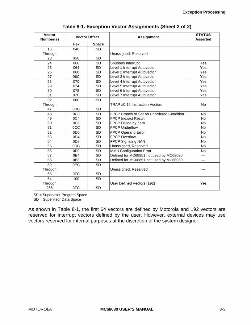
Exception Processing
MOTOROLA
MC68030 USER’S MANUAL
8-3
SP = Supervisor Program SpaceSD = Supervisor Data Space
As shown in Table 8-1, the first 64 vectors are defined by Motorola and 192 vectors arereserved for interrupt vectors defined by the user. However, external devices may usevectors reserved for internal purposes at the discretion of the system designer.
Table 8-1. Exception Vector Assignments (Sheet 2 of 2)
Vector Number(s)
Vector Offset AssignmentSTATUS Asserted
Hex Space
16Through
23
040
05C
SD
SDUnassigned, Reserved —
24252627
06006406806C
SDSDSDSD
Spurious InterruptLevel 1 Interrupt AutovectorLevel 2 Interrupt AutovectorLevel 3 Interrupt Autovector
YesYesYesYes
28293031
07007407807C
SDSDSDSD
Level 4 Interrupt AutovectorLevel 5 Interrupt AutovectorLevel 6 Interrupt AutovectorLevel 7 Interrupt Autovector
YesYesYesYes
32Through
47
080
0BC
SD
SDTRAP #0-15 Instruction Vectors No
48495051
0C00C40C80CC
SDSDSDSD
FPCP Branch or Set on Unordered ConditionFPCP Inexact ResultFPCP Divide by ZeroFPCP Underflow
NoNoNoNo
52535455
0D00D40D80DC
SDSDSDSD
FPCP Operand ErrorFPCP OverflowFPCP Signaling NANUnassigned, Reserved
NoNoNoNo
565758
0E00E40E8
SDSDSD
MMU Configuration ErrorDefined for MC68851 not used by MC68030Defined for MC68851 not used by MC68030
No——
59Through
63
0EC
0FC
SD
SDUnassigned, Reserved —
64Through
255
100
3FC
SD
SDUser Defined Vectors (192) Yes
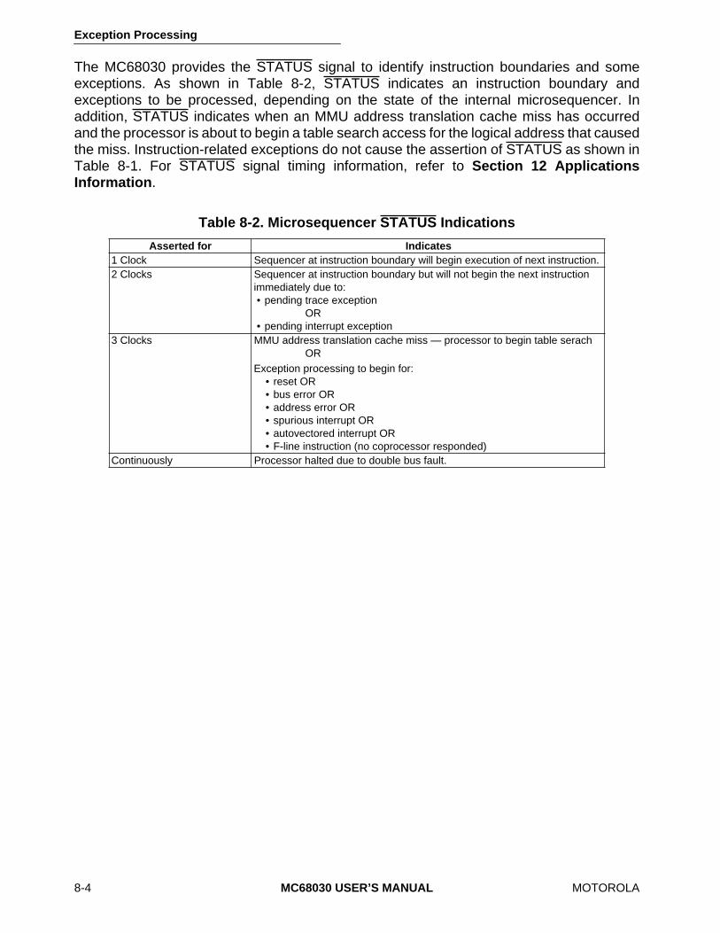
Exception Processing
8-4
MC68030 USER’S MANUAL
MOTOROLA
The MC68030 provides the STATUS signal to identify instruction boundaries and someexceptions. As shown in Table 8-2, STATUS indicates an instruction boundary andexceptions to be processed, depending on the state of the internal microsequencer. Inaddition, STATUS indicates when an MMU address translation cache miss has occurredand the processor is about to begin a table search access for the logical address that causedthe miss. Instruction-related exceptions do not cause the assertion of STATUS as shown inTable 8-1. For STATUS signal timing information, refer to
Section 12 ApplicationsInformation
.
Table 8-2. Microsequencer STATUS Indications
Asserted for Indicates
1 Clock Sequencer at instruction boundary will begin execution of next instruction.2 Clocks Sequencer at instruction boundary but will not begin the next instruction
immediately due to:
•
pending trace exceptionOR
•
pending interrupt exception3 Clocks MMU address translation cache miss — processor to begin table serach
ORException processing to begin for:
•
reset OR
•
bus error OR
•
address error OR
•
spurious interrupt OR
•
autovectored interrupt OR
•
F-line instruction (no coprocessor responded)Continuously Processor halted due to double bus fault.

Exception Processing
MOTOROLA
MC68030 USER’S MANUAL
8-5
8.1.1 Reset Exception
Assertion by external hardware of the RESET signal causes a reset exception. For detailson the requirements for the assertion of RESET, refer to
7.8 Reset Operation
.
The reset exception has the highest priority of any exception; it provides for systeminitialization and recovery from catastrophic failure. When reset is recognized, it aborts anyprocessing in progress, and that processing cannot be recovered. Figure 8-1 is a flowchartof the reset exception, which performs the following operations:
1. Clears both trace bits in the status register to disable tracing.
2. Places the processor in the interrupt mode of the supervisor privilege level by setting the supervisor bit and clearing the master bit in the status register.
3. Sets the processor interrupt priority mask to the highest priority level (level 7).
4. Initializes the vector base register to zero ($00000000).
5. Clears the enable, freeze, and burst enable bits for both on-chip caches and the write-allocate bit for the data cache in the cache control register.
6. Invalidates all entries in the instruction and data caches.
7. Clears the enable bit in the translation control register and the enable bits in both trans-parent translation registers of the MMU.
8. Generates a vector number to reference the reset exception vector (two long words) at offset zero in the supervisor program address space.
9. Loads the first long word of the reset exception vector into the interrupt stack pointer.
10. Loads the second long word of the reset exception vector into the program counter.
After the initial instruction prefetches, program execution begins at the address in theprogram counter. The reset exception does not flush the address translation cache (ATC),nor does it save the value of either the program counter or the status register.
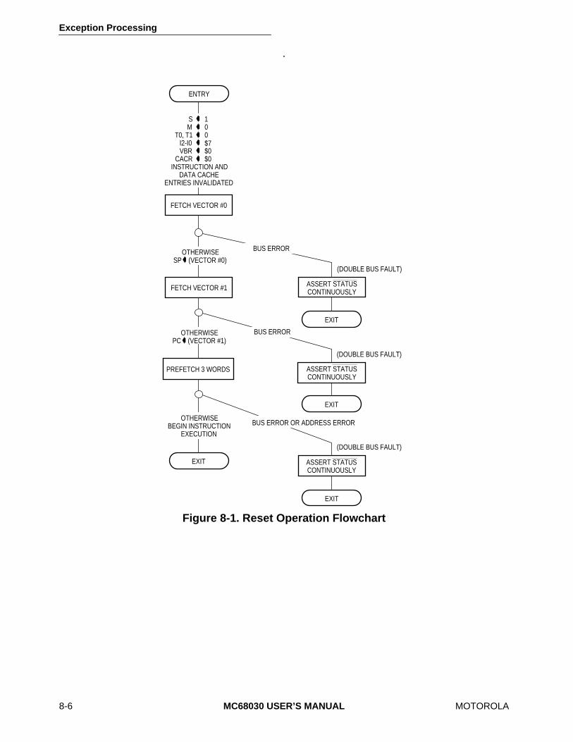
Exception Processing
8-6
MC68030 USER’S MANUAL
MOTOROLA
.
Figure 8-1. Reset Operation Flowchart
BUS ERROR OR ADDRESS ERROR
OTHERWISESP (VECTOR #0)
EXIT
FETCH VECTOR #0
(DOUBLE BUS FAULT)
SM
T0, T1I2-I0VBR
CACR
100$7$0$0
➧➧➧➧➧➧
(DOUBLE BUS FAULT)
(DOUBLE BUS FAULT)
ENTRY
OTHERWISEBEGIN INSTRUCTION
EXECUTION
BUS ERROROTHERWISE
INSTRUCTION ANDDATA CACHE
ENTRIES INVALIDATED
➧
FETCH VECTOR #1
PC (VECTOR #1)
➧
PREFETCH 3 WORDS
EXIT
EXIT
BUS ERROR
EXIT
ASSERT STATUSCONTINUOUSLY
ASSERT STATUSCONTINUOUSLY
ASSERT STATUSCONTINUOUSLY
Exception Processing
MOTOROLA
MC68030 USER’S MANUAL
8-7
As described in
7.5.4 Double Bus Fault
, if bus error or address error occur during theexception processing sequence for a reset, a double bus fault occurs. The processor halts,and the STATUS signal is asserted continuously to indicate the halted condition.
Execution of the reset instruction does not cause a reset exception, nor does it affect anyinternal registers, but it does cause the MC68030 to assert the RESET signal, resetting allexternal devices.
8.1.2 Bus Error Exception
A bus error exception occurs when external logic aborts a bus cycle by asserting the BERRinput signal. If the aborted bus cycle is a data access, the processor immediately beginsexception processing. If the aborted bus cycle is an instruction prefetch, the processor maydelay taking the exception until it attempts to use the prefetched information. The assertionof the BERR signal during the second, third, or fourth access of a burst operation does notcause a bus error exception, but the burst is aborted. Refer to
6.1.3.2 Burst Mode Filling
and
7.5.1 Bus Errors
for details on the effects of bus errors during burst operation.
A bus error exception also occurs when the MMU detects that a successful addresstranslation is not possible. Furthermore, when an ATC miss occurs and an external buscycle is required, the MMU must abort the bus cycle, search the translation tables in memoryfor the mapping, and then retry the bus cycle. If a valid translation for the logical address isnot available due to a problem encountered during the table search (the attempt to accessthe appropriate page descriptor in the translation tables for that page), a bus error exceptionoccurs when the aborted bus cycle is retried.
The problem encountered could be a limit violation, an invalid descriptor, or the assertion ofthe BERR signal during a bus cycle used to access the translation tables. A miss in the ATCcauses the processor to automatically initiate a table search but does not cause a bus errorexception unless one of the specific conditions mentioned above is encountered.
Exception Processing
8-8
MC68030 USER’S MANUAL
MOTOROLA
The processor begins exception processing for a bus error by making an internal copy of thecurrent status register. The processor then enters the supervisor privilege level (by settingthe S bit in the status register) and clears the trace bits. The processor generates exceptionvector number 2 for the bus error vector. It saves the vector offset, program counter, and theinternal copy of the status register on the stack. The saved program counter value is thelogical address of the instruction that was executing at the time the fault was detected. Thisis not necessarily the instruction that initiated the bus cycle, since the processor overlapsexecution of instructions. The processor also saves the contents of some of its internalregisters. The information saved on the stack is sufficient to identify the cause of the busfault and recover from the error.
For efficiency, the MC68030 uses two different bus error stack frame formats. When the buserror exception is taken at an instruction boundary, less information is required to recoverfrom the error, and the processor builds the short bus fault stack frame as shown in Table8-7. When the exception is taken during the execution of an instruction, the processor mustsave its entire state for recovery and uses the long bus fault stack frame shown in Table 8-7. The format code in the stack frame distinguishes the two stack frame formats. Stackframe formats are described in detail in
8.4 Exception Stack Frame Formats
.
If a bus error occurs during the exception processing for a bus error, address error, or resetor while the processor is loading internal state information from the stack during theexecution of an RTE instruction, a double bus fault occurs, and the processor enters thehalted state as indicated by the continuous assertion of the STATUS signal. In this case, theprocessor does not attempt to alter the current state of memory. Only an external RESETcan restart a processor halted by a double bus fault.
8.1.3 Address Error Exception
An address error exception occurs when the processor attempts to prefetch an instructionfrom an odd address. This exception is similar to a bus error exception, but is internallyinitiated. A bus cycle is not executed, and the processor begins exception processingimmediately. After exception processing commences, the sequence is the same as that forbus error exceptions described in the preceding paragraphs, except that the vector numberis 3 and the vector offset in the stack frame refers to the address error vector. Either a shortor long bus fault stack frame may be generated. If an address error occurs during theexception processing for a bus error, address error, or reset, a double bus fault occurs.
Exception Processing
MOTOROLA
MC68030 USER’S MANUAL
8-9
8.1.4 Instruction Trap Exception
Certain instructions are used to explicitly cause trap exceptions. The TRAP #n instructionalways forces an exception and is useful for implementing system calls in user programs.The TRAPcc, TRAPV, cpTRAPcc, CHK, and CHK2 instructions force exceptions if the userprogram detects an error, which may be an arithmetic overflow or a subscript value that isout of bounds.
The DIVS and DIVU instructions force exceptions if a division operation is attempted with adivisor of zero.
When a trap exception occurs, the processor copies the status register internally, enters thesupervisor privilege level, and clears the trace bits. If tracing is enabled for the instructionthat caused the trap, a trace exception is taken after the RTE instruction from the traphandler is executed, and the trace corresponds to the trap instruction; the trap handlerroutine is not traced. The processor generates a vector number according to the instructionbeing executed; for the TRAP #n instruction, the vector number is 32 plus n. The stack framesaves the trap vector offset, the program counter, and the internal copy of the status registeron the supervisor stack. The saved value of the program counter is the logical address ofthe instruction following the instruction that caused the trap. For all instruction traps otherthan TRAP #n, a pointer to the instruction that caused the trap is also saved. Instructionexecution resumes at the address in the exception vector after the required instructionprefetches.
8.1.5 Illegal Instruction and Unimplemented Instruction Exceptions
An illegal instruction is an instruction that contains any bit pattern in its first word that doesnot correspond to the bit pattern of the first word of a valid MC68030 instruction or is aMOVEC instruction with an undefined register specification field in the first extension word.An illegal instruction exception corresponds to vector number 4 and occurs when theprocessor attempts to execute an illegal instruction.

Exception Processing
8-10
MC68030 USER’S MANUAL
MOTOROLA
An illegal instruction exception is also taken if a breakpoint acknowledge bus cycle (see
7.4.2 Breakpoint Acknowledge Cycle
) is terminated with the assertion of the bus errorsignal. This implies that the external circuitry did not supply an instruction word to replacethe BKPT instruction word in the instruction pipe.
Instruction word patterns with bits [15:12] equal to $A are referred to as unimplementedinstructions with A-line opcodes. When the processor attempts to execute anunimplemented instruction with an A-line opcode, an exception is generated with vectornumber 10, permitting efficient emulation of unimplemented instructions.
Instructions that have word patterns with bits [15:12] equal to $F, bits [11:9] equal to $0, anddefined word patterns for subsequent words are legal MMU instructions. Instructions thathave bits [15:12] of the first words equal to $F, bits [11:9] equal to $0, and undefined patternsin subsequent words are treated as unimplemented instructions with F-line opcodes whenexecution is attempted in supervisor mode. When execution of the same instruction isattempted in user mode, a privilege violation exception is taken. The exception vectornumber for an unimplemented instruction with an F-line opcode is number 11.
The word patterns with bits [15:12] equal to $F and bits [11:9] not equal to zero are used forcoprocessor instructions. When the processor identifies a coprocessor instruction, it runs abus cycle referencing CPU space type $2 (refer to
4.2 Address Space Types
) andaddressing one of seven coprocessors (1-7, according to bits [11:9]). If the addressedcoprocessor is not included in the system and the cycle terminates with the assertion of thebus error signal, the instruction takes an unimplemented instruction (F-line opcode)exception. The system can emulate the functions of the coprocessor with an F-lineexception handler. Refer to
Section 10 Coprocessor Interface Description
for moredetails.

Exception Processing
MOTOROLA
MC68030 USER’S MANUAL
8-11
Exception processing for illegal and unimplemented instructions is similar to that forinstruction traps. When the processor has identified an illegal or unimplemented instruction,it initiates exception processing instead of attempting to execute the instruction. Theprocessor copies the status register, enters the supervisor privilege level, and clears thetrace bits, disabling further tracing. The processor generates the vector number, either 4,10, or 11, according to the exception type. The illegal or unimplemented instruction vectoroffset, current program counter, and copy of the status register are saved on the supervisorstack, with the saved value of the program counter being the address of the illegal orunimplemented instruction. Instruction execution resumes at the address contained in theexception vector. It is the responsibility of the handling routine to adjust the stacked programcounter if the instruction is emulated in software or is to be skipped on return from thehandler.
8.1.6 Privilege Violation Exception
To provide system security, the following instructions are privileged:
ANDI TO SR
EOR to SR
cpRESTORE
cpSAVE
MOVE from SR
MOVE to SR
MOVE USP
MOVEC
MOVES
ORI to SR
PFLUSH
PLOAD
PMOVE
PTEST
RESET
RTE
STOP
An attempt to execute one of the privileged instructions while at the user privilege levelcauses a privilege violation exception. Also, a privilege violation exception occurs if acoprocessor requests a privilege check and the processor is at the user level.
Exception Processing
8-12
MC68030 USER’S MANUAL
MOTOROLA
Exception processing for privilege violations is similar to that for illegal instructions. Whenthe processor identifies a privilege violation, it begins exception processing before executingthe instruction. The processor copies the status register, enters the supervisor privilegelevel, and clears the trace bits. The processor generates vector number 8, the privilegeviolation exception vector, and saves the privilege violation vector offset, the currentprogram counter value, and the internal copy of the status register on the supervisor stack.The saved value of the program counter is the logical address of the first word of theinstruction that caused the privilege violation. Instruction execution resumes after therequired prefetches from the address in the privilege violation exception vector.
8.1.7 Trace Exception
To aid in program development, the M68000 processors include instruction-by-instructiontracing capability. The MC68030 can be programmed to trace all instructions or onlyinstructions that change program flow. In the trace mode, an instruction generates a traceexception after it completes execution, allowing a debugger program to monitor executionof a program.
The T1 and T0 bits in the supervisor portion of the status register control tracing. The stateof these bits when an instruction begins execution determines whether the instructiongenerates a trace exception after the instruction completes. Clearing both T bits disablestracing, and instruction execution proceeds normally. Clearing the T1 bit and setting the T0bit causes an instruction that forces a change of flow to take a trace exception. Instructionsthat increment the program counter normally do not take the trace exception. Instructionsthat are traced in this mode include all branches, jumps, instruction traps, returns, andcoprocessor instructions that modify the program counter flow. This mode also includesstatus register manipulations, because the processor must re-prefetch instruction words tofill the pipe again any time an instruction that can modify the status register is executed. Theexecution of the BKPT instruction causes a change of flow if the opcode replacing the BKPTis an instruction that causes a change of flow (i.e., a jump, branch, etc.). Setting the T1 bitand clearing the T0 bit causes the execution of all instructions to force trace exceptions.Table 8-3 shows the trace mode selected by each combination of T1 and T0.
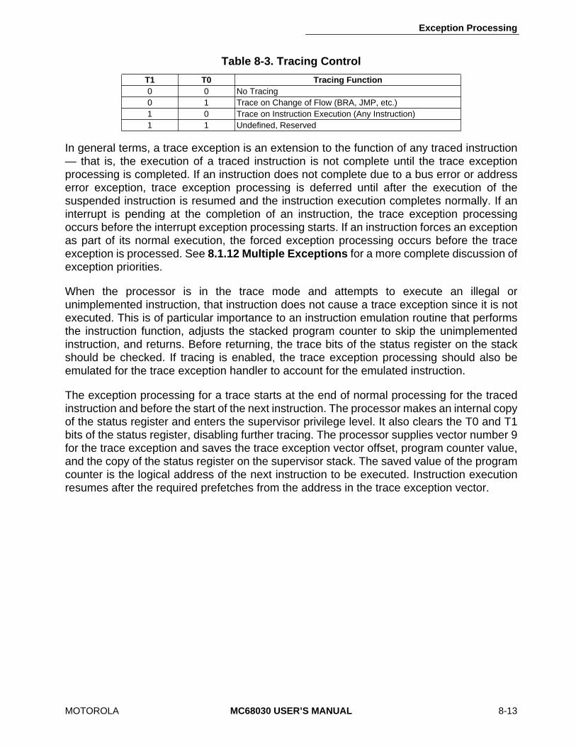
Exception Processing
MOTOROLA
MC68030 USER’S MANUAL
8-13
In general terms, a trace exception is an extension to the function of any traced instruction— that is, the execution of a traced instruction is not complete until the trace exceptionprocessing is completed. If an instruction does not complete due to a bus error or addresserror exception, trace exception processing is deferred until after the execution of thesuspended instruction is resumed and the instruction execution completes normally. If aninterrupt is pending at the completion of an instruction, the trace exception processingoccurs before the interrupt exception processing starts. If an instruction forces an exceptionas part of its normal execution, the forced exception processing occurs before the traceexception is processed. See
8.1.12 Multiple Exceptions
for a more complete discussion ofexception priorities.
When the processor is in the trace mode and attempts to execute an illegal orunimplemented instruction, that instruction does not cause a trace exception since it is notexecuted. This is of particular importance to an instruction emulation routine that performsthe instruction function, adjusts the stacked program counter to skip the unimplementedinstruction, and returns. Before returning, the trace bits of the status register on the stackshould be checked. If tracing is enabled, the trace exception processing should also beemulated for the trace exception handler to account for the emulated instruction.
The exception processing for a trace starts at the end of normal processing for the tracedinstruction and before the start of the next instruction. The processor makes an internal copyof the status register and enters the supervisor privilege level. It also clears the T0 and T1bits of the status register, disabling further tracing. The processor supplies vector number 9for the trace exception and saves the trace exception vector offset, program counter value,and the copy of the status register on the supervisor stack. The saved value of the programcounter is the logical address of the next instruction to be executed. Instruction executionresumes after the required prefetches from the address in the trace exception vector.
Table 8-3. Tracing Control
T1 T0 Tracing Function
0 0 No Tracing0 1 Trace on Change of Flow (BRA, JMP, etc.)1 0 Trace on Instruction Execution (Any Instruction)1 1 Undefined, Reserved

Exception Processing
8-14
MC68030 USER’S MANUAL
MOTOROLA
The STOP instruction does not perform its function when it is traced. A STOP instruction thatbegins execution with T1=1 and T0=0 forces a trace exception after it loads the statusregister. Upon return from the trace handler routine, execution continues with the instructionfollowing the STOP, and the processor never enters the stopped condition.
8.1.8 Format Error Exception
Just as the processor checks that prefetched instructions are valid, the processor (with theaid of a coprocessor, if needed) also performs some checks of data values for controloperations, including the coprocessor state frame format word for a cpRESTORE instructionand the stack frame format for an RTE instruction.
The RTE instruction checks the validity of the stack format code. For long bus cycle faultformat frames, the RTE instruction also compares the internal version number of theprocessor to that contained in the frame at memory location SP+54 (SP+$36). This checkensures that the processor can correctly interpret internal state information from the stackframe.
The cpRESTORE instruction passes the format word of the coprocessor state frame to thecoprocessor for validation. If the coprocessor does not recognize the format value, it signalsthe MC68030 to take a format error exception. Refer to
Section 10 Coprocessor InterfaceDescription
for details of coprocessor-related exceptions.
If any of the checks previously described determine that the format of the stacked data isimproper, the instruction generates a format error exception. This exception saves a shortformat stack frame, generates exception vector number 14, and continues execution at theaddress in the format exception vector. The stacked program counter value is the logicaladdress of the instruction that detected the format error.
8.1.9 Interrupt Exceptions
When a peripheral device requires the services of the MC68030 or is ready to sendinformation that the processor requires, it may signal the processor to take an interruptexception. The interrupt exception transfers control to a routine that responds appropriately.
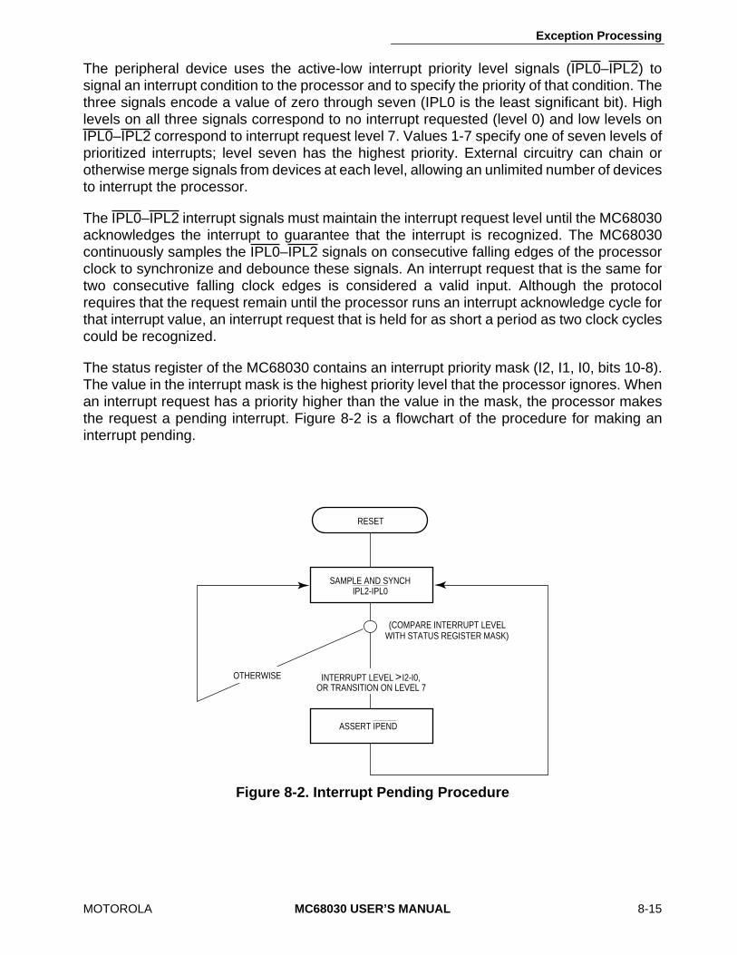
Exception Processing
MOTOROLA
MC68030 USER’S MANUAL
8-15
The peripheral device uses the active-low interrupt priority level signals (IPL0–IPL2) tosignal an interrupt condition to the processor and to specify the priority of that condition. Thethree signals encode a value of zero through seven (IPL0 is the least significant bit). Highlevels on all three signals correspond to no interrupt requested (level 0) and low levels onIPL0–IPL2 correspond to interrupt request level 7. Values 1-7 specify one of seven levels ofprioritized interrupts; level seven has the highest priority. External circuitry can chain orotherwise merge signals from devices at each level, allowing an unlimited number of devicesto interrupt the processor.
The IPL0–IPL2 interrupt signals must maintain the interrupt request level until the MC68030acknowledges the interrupt to guarantee that the interrupt is recognized. The MC68030continuously samples the IPL0–IPL2 signals on consecutive falling edges of the processorclock to synchronize and debounce these signals. An interrupt request that is the same fortwo consecutive falling clock edges is considered a valid input. Although the protocolrequires that the request remain until the processor runs an interrupt acknowledge cycle forthat interrupt value, an interrupt request that is held for as short a period as two clock cyclescould be recognized.
The status register of the MC68030 contains an interrupt priority mask (I2, I1, I0, bits 10-8).The value in the interrupt mask is the highest priority level that the processor ignores. Whenan interrupt request has a priority higher than the value in the mask, the processor makesthe request a pending interrupt. Figure 8-2 is a flowchart of the procedure for making aninterrupt pending.
Figure 8-2. Interrupt Pending Procedure
RESET
SAMPLE AND SYNCHIPL2-IPL0
ASSERT IPEND
(COMPARE INTERRUPT LEVELWITH STATUS REGISTER MASK)
OTHERWISE INTERRUPT LEVEL I2-I0,OR TRANSITION ON LEVEL 7
>

Exception Processing
8-16
MC68030 USER’S MANUAL
MOTOROLA
When several devices are connected to the same interrupt level, each device should holdits interrupt priority level constant until its corresponding interrupt acknowledge cycle toensure that all requests are processed.
Table 8-4 lists the interrupt levels, the states of IPL2-IPL0 that define each level, and themask value that allows an interrupt at each level.
*Indicates that no interrupt is requested.
Priority level 7, the nonmaskable interrupt (NMI), is a special case. Level 7 interrupts cannotbe masked by the interrupt priority mask, and they are transition sensitive. The processorrecognizes an interrupt request each time the external interrupt request level changes fromsome lower level to level 7, regardless of the value in the mask. Figure 8-3 shows twoexamples of interrupt recognitions, one for level 6 and one for level 7. When the MC68030processes a level 6 interrupt, the status register mask is automatically updated with a valueof 6 before entering the handler routine so that subsequent level 6 interrupts are masked.Provided no instruction that lowers the mask value is executed, the external request can belowered to level 3 and then raised back to level 6 and a second level 6 interrupt is notprocessed. However, if the MC68030 is handling a level 7 interrupt (status register mask setto 7) and the external request is lowered to level 3 and than raised back to level 7, a secondlevel 7 interrupt is processed. The second level 7 interrupt is processed because the level 7interrupt is transition sensitive. A level 7 interrupt is also generated by a level comparison ifthe request level and mask level are at seven and the priority mask is then set to a lowerlevel (with the MOVE to SR or RTE instruction, for example). As shown in Figure 8-3 for level6 interrupt request level and mask level, this is the case for all interrupt levels.
Table 8-4. Interrupt Levels and Mask Values
Requested Interrupt Level
Control Line StatusInterrupt Mask Level
Required for RecognitionIP2 IP1 IP0
0* High High High N/A*1 High High Low 02 High Low High 0-13 High Low Low 0-24 Low High High 0-35 Low High Low 0-46 Low Low High 0-57 Low Low Low 0-7
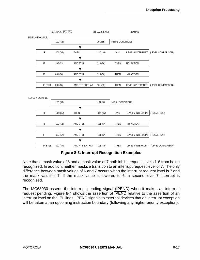
Exception Processing
MOTOROLA
MC68030 USER’S MANUAL
8-17
Note that a mask value of 6 and a mask value of 7 both inhibit request levels 1-6 from beingrecognized. In addition, neither masks a transition to an interrupt request level of 7. The onlydifference between mask values of 6 and 7 occurs when the interrupt request level is 7 andthe mask value is 7. If the mask value is lowered to 6, a second level 7 interrupt isrecognized.
The MC68030 asserts the interrupt pending signal (IPEND) when it makes an interruptrequest pending. Figure 8-4 shows the assertion of IPEND relative to the assertion of aninterrupt level on the IPL lines. IPEND signals to external devices that an interrupt exceptionwill be taken at an upcoming instruction boundary (following any higher priority exception).
Figure 8-3. Interrupt Recognition Examples
EXTERNAL IPL2-IPL0 SR MASK (I2-I0) ACTION
LEVEL 6 EXAMPLE:
INITIAL CONDITIONS100 ($3) 101 ($5)
(LEVEL COMPARISON)IF 001 ($6) THEN 110 ($6) AND LEVEL 6 INTERRUPT
IF 100 ($3) AND STILL 110 ($6) THEN NO ACTION
IF 001 ($6) AND STILL 110 ($6) THEN
IF STILL 001 ($6) AND RTE SO THAT 101 ($5) THEN LEVEL 6 INTERRUPT (LEVEL COMPARISON)
(TRANSITION)
(TRANSITION)
LEVEL 7 EXAMPLE:
INITIAL CONDITIONS100 ($3) 101 ($5)
IF 000 ($7) THEN 111 ($7) AND LEVEL 7 INTERRUPT
IF 100 ($3) AND STILL 111 ($7) THEN NO ACTION
IF 000 ($7) AND STILL 111 ($7) THEN
NO ACTION
IF STILL 000 ($7) AND RTE SO THAT 101 ($5) THEN LEVEL 7 INTERRUPT (LEVEL COMPARISON)
LEVEL 7 INTERRUPT

Exception Processing
8-18
MC68030 USER’S MANUAL
MOTOROLA
The state of the IPEND signal is internally checked by the processor once per instruction,independently of bus operation. In addition, it is checked during the second instructionprefetch associated with exception processing. Figure 8-5 is a flowchart of the interruptrecognition and associated exception processing sequence.
To predict the instruction boundary during which a pending interrupt is processed, the timingrelationship between the assertion of IPEND for that interrupt and the assertion of STATUSmust be examined. Figure 8-6 shows two examples of interrupt recognition. The firstassertion of STATUS after IPEND is denoted as STAT0. The next assertion of STATUS isdenoted as STAT1. If STAT0 begins on the falling edge of the clock immediately followingthe clock edge that caused IPEND to assert (as shown in example 1), STAT1 is at least twoclocks long, and, when there are no other pending exceptions, the interrupt is acknowledgedat the boundary defined by STAT1. If IPEND is asserted with more setup time to STAT0, theinterrupt may be acknowledged at the boundary defined by STAT0 (as shown in example2). In that case, STAT0 is asserted for two clocks, signaling this condition.
If no higher priority interrupt has been synchronized, the IPEND signal is negated duringstate 0 (S0) of an interrupt acknowledge cycle (refer to
7.4.1.1 Interrupt AcknowledgeCycle — Terminated Normally
), and the IPLx signals for the interrupt being acknowledgedcan be negated at this time.
Figure 8-4. Assertion of IPEND
CLK
IPL2-IPL0
IPEND
COMPARE REQUESTWITH MASK IN SR
ASSERT IPENDIPLs RECOGNIZED
IPLs SYNCHRONIZED
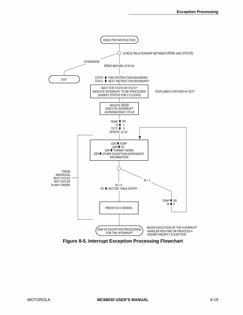
Exception Processing
MOTOROLA
MC68030 USER’S MANUAL
8-19
Figure 8-5. Interrupt Exception Processing Flowchart
TEMPS
T0,T1
SR10
➧➧➧
UPDATE 12-10
➧➧
➧➧
-(SP) TEMP-(SP) PC
-(SP) FORMAT WORD-(SP) OTHER EXCEPTION-DEPENDENT
ONCE PER INSTRUCTION
NEGATE IPENDEXECUTE INTERRUPT
ACKNOWLEDGE CYCLE
IPEND BEFORE STATUS
(CHECK RELATIONSHIP BETWEEN IPEND AND STATUS)
EXIT
OTHERWISE
M = 1
TEMP SRM 0
➧➧
M = 0PC VECTOR TABLE ENTRY
➧
PREFETCH 3 WORDS
END OF EXCEPTION PROCESSINGFOR THE INTERRUPT
BEGIN EXECUTION OF THE INTERRUPTHANDLER ROUTINE OR PROCESS AHIGHER PRIORITY EXCEPTION
THESEINDIVIDUAL
BUS CYCLESMAY OCCUR
IN ANY ORDER
WAIT FOR STAT0 OR STAT1*INDICATE INTERRUPT TO BE PROCESSED
(ASSERT STATUS FOR 2 CLOCKS)
STAT0 THIS INSTRUCTION BOUNDARY
➧
STAT1 NEXT INSTRUCTION BOUNDARY
➧
*EXPLAINED FURTHER IN TEXT
INFORMATION
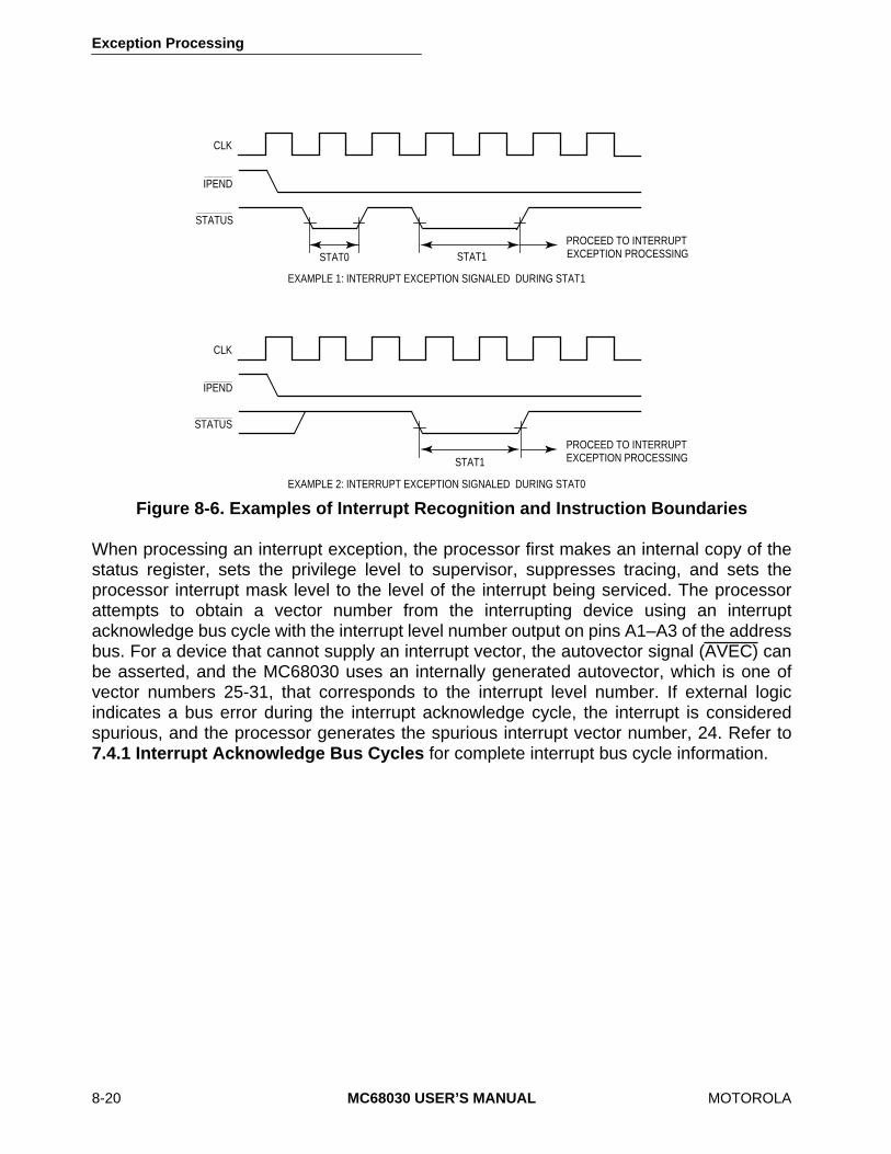
Exception Processing
8-20
MC68030 USER’S MANUAL
MOTOROLA
When processing an interrupt exception, the processor first makes an internal copy of thestatus register, sets the privilege level to supervisor, suppresses tracing, and sets theprocessor interrupt mask level to the level of the interrupt being serviced. The processorattempts to obtain a vector number from the interrupting device using an interruptacknowledge bus cycle with the interrupt level number output on pins A1–A3 of the addressbus. For a device that cannot supply an interrupt vector, the autovector signal (AVEC) canbe asserted, and the MC68030 uses an internally generated autovector, which is one ofvector numbers 25-31, that corresponds to the interrupt level number. If external logicindicates a bus error during the interrupt acknowledge cycle, the interrupt is consideredspurious, and the processor generates the spurious interrupt vector number, 24. Refer to7.4.1 Interrupt Acknowledge Bus Cycles for complete interrupt bus cycle information.
Figure 8-6. Examples of Interrupt Recognition and Instruction Boundaries
CLK
IPEND
STATUS
STAT0 STAT1
EXAMPLE 1: INTERRUPT EXCEPTION SIGNALED DURING STAT1
PROCEED TO INTERRUPTEXCEPTION PROCESSING
CLK
IPEND
STATUS
STAT1
EXAMPLE 2: INTERRUPT EXCEPTION SIGNALED DURING STAT0
PROCEED TO INTERRUPTEXCEPTION PROCESSING

Exception Processing
MOTOROLA MC68030 USER’S MANUAL 8-21
Once the vector number is obtained, the processor saves the exception vector offset,program counter value, and the internal copy of the status register on the active supervisorstack. The saved value of the program counter is the logical address of the instruction thatwould have been executed had the interrupt not occurred. If the interrupt was acknowledgedduring the execution of a coprocessor instruction, further internal information is saved on thestack so that the MC68030 can continue executing the coprocessor instruction when theinterrupt handler completes execution.
If the M bit of the status register is set, the processor clears the M bit and creates athrowaway exception stack frame on top of the interrupt stack as part of interrupt exceptionprocessing. This second frame contains the same program counter value and vector offsetas the frame created on top of the master stack, but has a format number of 1 instead of 0or 9. The copy of the status register saved on the throwaway frame is exactly the same asthat placed on the master stack except that the S bit is set in the version placed on theinterrupt stack. (It may or may not be set in the copy saved on the master stack.) Theresulting status register (after exception processing) has the S bit set and the M bit cleared.
The processor loads the address in the exception vector into the program counter, andnormal instruction execution resumes after the required prefetches for the interrupt handlerroutine.
Most M68000 Family peripherals use programmable interrupt vector numbers as part of theinterrupt request/acknowledge mechanism of the system. If this vector number is notinitialized after reset and the peripheral must acknowledge an interrupt request, theperipheral usually returns the vector number for the uninitialized interrupt vector, 15.
8.1.10 MMU Configuration ExceptionWhen the MC68030 executes a PMOVE instruction that attempts to move invalid data intothe TC, CRP, or SRP register of the MMU, the PMOVE instruction causes an MMUconfiguration exception. The exception is a post-instruction exception; it is processed afterthe instruction completes. The processor generates exception vector number 56 when anMMU configuration exception occurs. Refer to Section 9 Memory Management Unit for adescription of the valid configurations for the MMU registers.
Exception Processing
8-22 MC68030 USER’S MANUAL MOTOROLA
The processor copies the status register, enters the supervisor privilege level, and clearsthe trace bits. The processor saves the vector offset, the scanPC value (which points to thenext instruction), and the copy of the status register on the supervisor stack. It also savesthe logical address of the PMOVE instruction on the stack. Then the processor resumesnormal instruction execution after the required prefetches from the address in the exceptionvector.
8.1.11 Breakpoint Instruction ExceptionTo use the MC68030 in a hardware emulator, it must provide a means of insertingbreakpoints in the emulator code and of performing appropriate operations at eachbreakpoint. For the MC68000 and MC68008, this can be done by inserting an illegalinstruction at the breakpoint and detecting the illegal instruction exception from its vectorlocation. However, since the vector base register on the MC68010, MC68020, andMC68030 allows arbitrary relocation of exception vectors, the exception address cannotreliably identify a breakpoint. The MC68020 and MC68030 processors provide a breakpointcapability with a set of breakpoint instructions, $4848-$484F, for eight unique breakpoints.The breakpoint facility also allows external hardware to monitor the execution of a programresiding in the on-chip instruction cache without severe performance degradation.
When the MC68030 executes a breakpoint instruction, it performs a breakpointacknowledge cycle (read cycle) from CPU space type $0 with address lines A2-A4corresponding to the breakpoint number. Refer to Figure 7-44 for the CPU space type $0addresses and to 7.4.2 Breakpoint Acknowledge Cycle for a description of the breakpointacknowledge cycle. The external hardware can return either BERR, DSACKx, or STERMwith an instruction word on the data bus. If the bus cycle terminates with BERR, theprocessor performs illegal instruction exception processing. If the bus cycle terminates withDSACKx or STERM, the processor uses the data returned to replace the breakpointinstruction in the internal instruction pipe and begins execution of that instruction. Theremainder of the pipe remains unaltered. In addition, no stacking or vector fetching isinvolved with the execution of the instruction. Figure 8-7 is a flowchart of the breakpointinstruction execution.
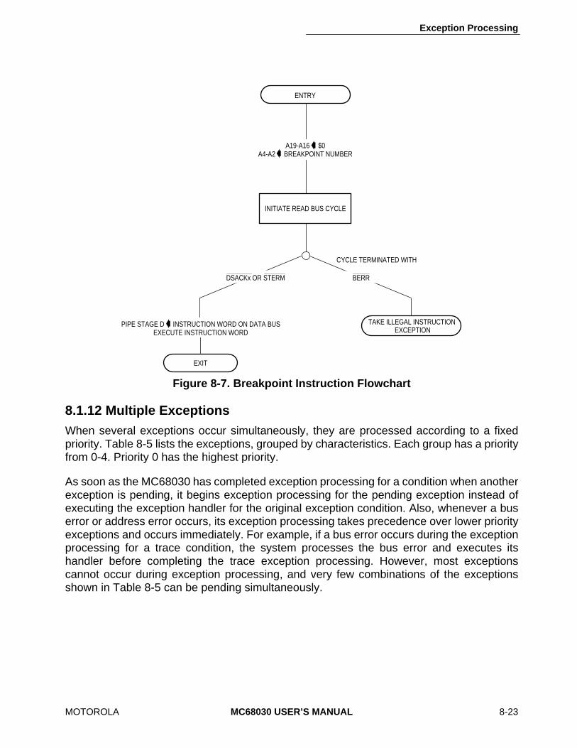
Exception Processing
MOTOROLA MC68030 USER’S MANUAL 8-23
8.1.12 Multiple ExceptionsWhen several exceptions occur simultaneously, they are processed according to a fixedpriority. Table 8-5 lists the exceptions, grouped by characteristics. Each group has a priorityfrom 0-4. Priority 0 has the highest priority.
As soon as the MC68030 has completed exception processing for a condition when anotherexception is pending, it begins exception processing for the pending exception instead ofexecuting the exception handler for the original exception condition. Also, whenever a buserror or address error occurs, its exception processing takes precedence over lower priorityexceptions and occurs immediately. For example, if a bus error occurs during the exceptionprocessing for a trace condition, the system processes the bus error and executes itshandler before completing the trace exception processing. However, most exceptionscannot occur during exception processing, and very few combinations of the exceptionsshown in Table 8-5 can be pending simultaneously.
Figure 8-7. Breakpoint Instruction Flowchart
EXIT
ENTRY
A19-A16 $0A4-A2 BREAKPOINT NUMBER
➧➧
INITIATE READ BUS CYCLE
DSACKx OR STERM BERR
CYCLE TERMINATED WITH
PIPE STAGE D INSTRUCTION WORD ON DATA BUSEXECUTE INSTRUCTION WORD
➧ TAKE ILLEGAL INSTRUCTIONEXCEPTION
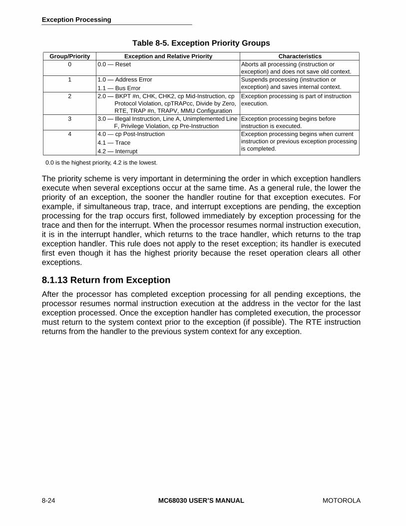
Exception Processing
8-24 MC68030 USER’S MANUAL MOTOROLA
0.0 is the highest priority, 4.2 is the lowest.
The priority scheme is very important in determining the order in which exception handlersexecute when several exceptions occur at the same time. As a general rule, the lower thepriority of an exception, the sooner the handler routine for that exception executes. Forexample, if simultaneous trap, trace, and interrupt exceptions are pending, the exceptionprocessing for the trap occurs first, followed immediately by exception processing for thetrace and then for the interrupt. When the processor resumes normal instruction execution,it is in the interrupt handler, which returns to the trace handler, which returns to the trapexception handler. This rule does not apply to the reset exception; its handler is executedfirst even though it has the highest priority because the reset operation clears all otherexceptions.
8.1.13 Return from ExceptionAfter the processor has completed exception processing for all pending exceptions, theprocessor resumes normal instruction execution at the address in the vector for the lastexception processed. Once the exception handler has completed execution, the processormust return to the system context prior to the exception (if possible). The RTE instructionreturns from the handler to the previous system context for any exception.
Table 8-5. Exception Priority Groups
Group/Priority Exception and Relative Priority Characteristics0 0.0 — Reset Aborts all processing (instruction or
exception) and does not save old context.1 1.0 — Address Error
1.1 — Bus ErrorSuspends processing (instruction or exception) and saves internal context.
2 2.0 — BKPT #n, CHK, CHK2, cp Mid-Instruction, cp Protocol Violation, cpTRAPcc, Divide by Zero, RTE, TRAP #n, TRAPV, MMU Configuration
Exception processing is part of instruction execution.
3 3.0 — Illegal Instruction, Line A, Unimplemented Line F, Privilege Violation, cp Pre-Instruction
Exception processing begins before instruction is executed.
4 4.0 — cp Post-Instruction4.1 — Trace4.2 — Interrupt
Exception processing begins when current instruction or previous exception processing is completed.
Exception Processing
MOTOROLA MC68030 USER’S MANUAL 8-25
When the processor executes an RTE instruction, it examines the stack frame on top of theactive supervisor stack to determine if it is a valid frame and what type of context restorationit requires. This section describes the processing for each of the stack frame types; refer to8.3 COPROCESSOR CONSIDERATIONS for a description of the stack frame type formats.
For a normal four-word frame, the processor updates the status register and programcounter with the data read from the stack, increments the stack pointer by eight, andresumes normal instruction execution.
For the throwaway four-word stack, the processor reads the status register value from theframe, increments the active stack pointer by eight, updates the status register with thevalue read from the stack, and then begins RTE processing again, as shown in Figure 8-8.The processor reads a new format word from the stack frame on top of the active stack(which may or may not be the same stack used for the previous operation) and performs theproper operations corresponding to that format. In most cases, the throwaway frame is onthe interrupt stack and when the status register value is read from the stack, the S and Mbits are set. In that case, there is a normal four-word frame or a ten-word coprocessor mid-instruction frame on the master stack. However, the second frame may be any format (evenanother throwaway frame) and may reside on any of the three system stacks.
For the six-word stack frame, the processor restores the status register and program countervalues from the stack, increments the active supervisor stack pointer by 12, and resumesnormal instruction execution.
For the coprocessor mid-instruction stack frame, the processor reads the status register,program counter, instruction address, internal register values, and the evaluated effectiveaddress from the stack, restores these values to the corresponding internal registers, andincrements the stack pointer by 20. The processor then reads from the response register ofthe coprocessor that initiated the exception to determine the next operation to be performed.Refer to Section 10 Coprocessor Interface Description for details of coprocessor-relatedexceptions.
For both the short and long bus fault stack frames, the processor first checks the formatvalue on the stack for validity. In addition, for the long stack frame, the processor comparesthe version number in the stack with its own version number. The version number is locatedin the most significant nibble (bits 15-12) of the word at location SP+$36 in the long stackframe. This validity check is required in a multiprocessor system to ensure that the data isproperly interpreted by the RTE instruction. The RTE instruction also reads from both endsof the stack frame to make sure it is accessible. If the frame is invalid or inaccessible, theprocessor takes a format error or a bus error exception, respectively. Otherwise, theprocessor reads the entire frame into the proper internal registers, deallocates the stack,and resumes normal processing. Once the processor begins to load the frame to restore itsinternal state, the assertion of the BERR signal causes the processor to enter the haltedstate with the continuous assertion of the STATUS signal. Refer to 8.2 Bus Fault Recoveryfor a description of the processing that occurs after the frame is read into the internalregisters.
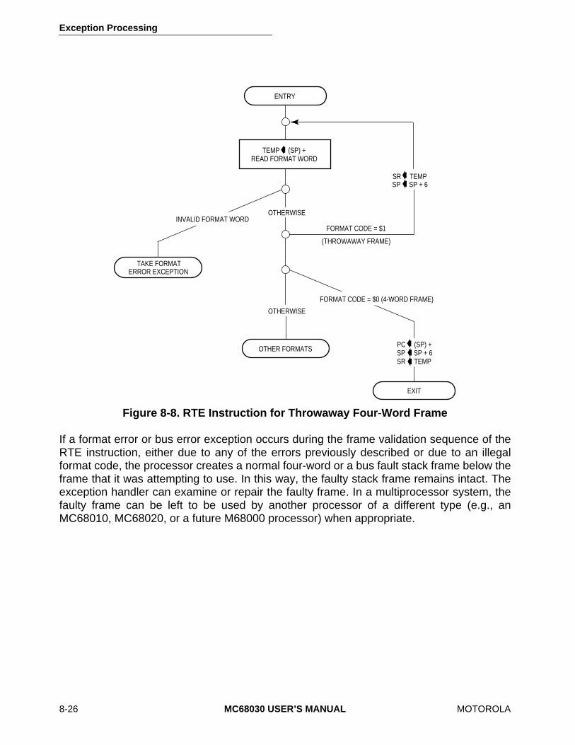
Exception Processing
8-26 MC68030 USER’S MANUAL MOTOROLA
If a format error or bus error exception occurs during the frame validation sequence of theRTE instruction, either due to any of the errors previously described or due to an illegalformat code, the processor creates a normal four-word or a bus fault stack frame below theframe that it was attempting to use. In this way, the faulty stack frame remains intact. Theexception handler can examine or repair the faulty frame. In a multiprocessor system, thefaulty frame can be left to be used by another processor of a different type (e.g., anMC68010, MC68020, or a future M68000 processor) when appropriate.
Figure 8-8. RTE Instruction for Throwaway Four-Word Frame
ENTRY
SR TEMPSP SP + 6
➧
➧
TEMP (SP) +READ FORMAT WORD
➧
OTHERWISE
FORMAT CODE = $1
(THROWAWAY FRAME)
FORMAT CODE = $0 (4-WORD FRAME)
OTHERWISE
PC (SP) +SP SP + 6SR TEMP
➧➧➧
EXIT
OTHER FORMATS
INVALID FORMAT WORD
TAKE FORMATERROR EXCEPTION
Exception Processing
MOTOROLA MC68030 USER’S MANUAL 8-27
8.2 BUS FAULT RECOVERYAn address error exception or a bus error exception indicates a bus fault. The saving of theprocessor state for a bus error or address error is described in 8.1.2 Bus Error Exception,and the restoring of the processor state by an RTE instruction is described in 8.1.13 Returnfrom Exception
Processor accesses of either data items or the instruction stream can result in bus errors.When a bus error exception occurs while accessing a data item, the exception is takenimmediately after the bus cycle terminates. Bus errors reported by the on-chip MMU are alsoprocessed immediately. A bus error occurring during an instruction stream access is notprocessed until the processor attempts to use the information (if ever) that the access shouldhave provided. For instruction faults, when the short format frame applies, the address ofthe pipe stage B word is the value in the program counter plus four, and the address of thestage C word is the value in the program counter plus two. For the long format, the long wordat SP+$24 contains the address of the stage B word; the address of the stage C word is theaddress of the stage B word minus two. Address error faults occur only for instruction streamaccesses, and the exceptions are taken before the bus cycles are attempted.

Exception Processing
8-28 MC68030 USER’S MANUAL MOTOROLA
8.2.1 Special Status Word (SSW)The internal SSW (see Figure 8-9) is one of several registers saved as part of the bus faultexception stack frame. Both the short bus cycle fault format and the long bus cycle faultformat include this word at offset $A. The bus cycle fault stack frame formats are describedin detail at the end of this section.
FC — Fault on stage C of the instruction pipeFB — Fault on stage B of the instruction pipeRC — Rerun flag for stage C of the instruction pipe*RB — Rerun flag for stage B of the instruction pipe*DF — Fault/rerun flag for data cycle*RM — Read-modify-write on data cycleRW — Read/write for data cycle — 1=read, 0=writeSIZE — Size code for data cycleFC2-FC0 — Address space for data cycle*1=Rerun Faulted bus Cycle, or run pending prefetch 0=Do not rerun bus sycle X=For internal use only
Figure 8-9. Special Status Word (SSW)
The SSW information indicates whether the fault was caused by an access to the instructionstream, data stream, or both. The high-order half of the SSW contains two status bits eachfor the B and C stages of the instruction pipe. The fault bits (FB and FC) indicate that theprocessor attempted to use a stage (B or C) and found it to be marked invalid due to a buserror on the prefetch for that stage. The fault bits can be used by a bus error handler todetermine the cause(s) of a bus error exception. The rerun flag bits (RB and RC) are set toindicate that a fault occurred during a prefetch for the corresponding stage. A rerun bit isalways set when the corresponding fault bit is set. The rerun bits indicate that the word in astage of the instruction pipe is invalid, and the state of the bits can be used by a handler torepair the values in the pipe after an address error or a bus error, if necessary. If a rerun bitis set when the processor executes an RTE instruction, the processor may execute a buscycle to prefetch the instruction word for the corresponding stage of the pipe (if it is required).If the rerun and fault bits are set for a stage of the pipe, the RTE instruction automaticallyreruns the prefetch cycle for that stage. The address space for the bus cycle is the programspace for the privilege level indicated in the copy of the status register on the stack. If a rerunbit is cleared, the words on the stack for the corresponding stages of the pipe are acceptedas valid; the processor assumes that there is no prefetch pending for the correspondingstage and that software has repaired or filled the image of the stage, if necessary.
15 14 13 12 11 10 9 8 7 65 4
32
0
FC FB RC RB X X X DF RM RW SIZE XFC2-FC0

Exception Processing
MOTOROLA MC68030 USER’S MANUAL 8-29
If an address error exception occurs, the fault bits written to the stack frame are not set (theyare only set due to a bus error, as previously described), and the rerun bits alone show thecause of the exception. Depending on the state of the pipeline, either RB and RC are bothset, or RC alone is set. To correct the pipeline contents and continue execution of thesuspended instruction, software must place the correct instruction stream data in the stageC and/or stage B images requested by the rerun bits and clear the rerun bits. The leastsignificant half of the SSW applies to data cycles only. If the DF bit of the SSW is set, a datafault has occurred and caused the exception. If the DF bit is set when the processor readsthe stack frame, it reruns the faulted data access; otherwise, it assumes that the data inputbuffer value on the stack is valid for a read or that the data has been correctly written tomemory for a write (or that no data fault occurred). The RM bit of the SSW identifies a read-modify-write operation and the RW bit indicates whether the cycle was a read or writeoperation. The SIZE field indicates the size of the operand access, and the FC field specifiesthe address space for the data cycle. Data and instruction stream faults may be pendingsimultaneously; the fault handler should be able to recognize any combination of the FC, FB,RC, RB, and DF bits.
8.2.2 Using Software to Complete the Bus CyclesOne method of completing a faulted bus cycle is to use a software handler to emulate thecycle. This is the only method for correcting address errors. The handler should emulate thefaulted bus cycle in a manner that is transparent to the instruction that caused the fault. Forinstruction stream faults, the handler may need to run bus cycles for both the B and C stagesof the instruction pipe. The RB and RC bits identify the stages that may require a bus cycle;the FB and FC bits indicate that a stage was invalid when an attempt was made to use itscontents. Those stages must be repaired. For each faulted stage, the software handlershould copy the instruction word from the proper address space as indicated by the S bit ofthe copy of the status register saved on the stack to the image of the appropriate stage inthe stack frame. In addition, the handler must clear the rerun bit associated with the stagethat it has corrected. The handler should not change the fault bits FB and FC.
Exception Processing
8-30 MC68030 USER’S MANUAL MOTOROLA
To repair data faults (indicated by DF=1), the software should first examine the RM bit in theSSW to determine if the fault was generated during a read-modify-write operation. If RM=0,the handler should then check the R/W bit of the SSW to determine if the fault was causedby a read or a write cycle. For data write faults, the handler must transfer the properly sizeddata from the data output buffer (DOB) on the stack frame to the location indicated by thedata fault address in the address space defined by the SSW. (Both the DOB and the datafault address are part of the stack frame at SP+$18 and SP+$10, respectively.) Data readfaults only generate the long bus fault frame and the handler must transfer properly sizeddata from the location indicated by the fault address and address space to the image of thedata input buffer (DIB) at location SP+$2C of the long format stack frame. Byte, word, and3-byte[lz operands are right-justified in the 4-byte data buffers. In addition, the softwarehandler must clear the DF bit of the SSW to indicate that the faulted bus cycle has beencorrected.
To emulate a read-modify-write cycle, the exception handler must first read the operationword at the program counter address (SP+2 of the stack frame). This word identifies theCAS, CAS2, or TAS instruction that caused the fault. Then the handler must emulate thisentire instruction (which may consist of up to four long word transfers) and update thecondition code portion of the status register appropriately, because the RTE instructionexpects the entire operation to have been completed if the RM bit is set and the DF bit iscleared. This is true even if the fault occurred on the first read cycle.
To emulate the entire instruction, the handler must save the data and address registers forthe instruction (with a MOVEM instruction, for example). Next, the handler reads andmodifies (if necessary) the memory location. It clears the DF bit in the SSW of the stackframe and modifies the condition codes in the status register copy and the copies of any dataor address registers required for the CAS and CAS2 instructions. Last, the handler restoresthe registers that it saved at the beginning of the emulation. Except for the data input buffer(DIB), the copy of the status register, and the SSW, the handler should not modify a bus faultstack frame. The only bits in the SSW that may be modified are DF, RB, and RC; all otherbits, including those defined for internal use, must remain unchanged.
Address error faults must be repaired in software. Address error faults can be distinguishedfrom bus error faults by the value in the vector offset field of the format word.

Exception Processing
MOTOROLA MC68030 USER’S MANUAL 8-31
8.2.3 Completing the Bus Cycles with RteAnother method of completing a faulted bus cycle is to allow the processor to rerun the buscycles during execution of the RTE instruction that terminates the exception handler. Thismethod cannot be used to recover from address errors. The RTE instruction is alwaysexecuted. Unless the handler routine has corrected the error and cleared the fault (andcleared the rerun and DF bits of the SSW), the RTE instruction can complete the buscycle(s). If the DF bit is still set at the time of the RTE execution, the faulted data cycle isrerun by the RTE instruction. If the fault bit for a stage of the pipe is set and thecorresponding rerun bit was not cleared by the software, the RTE reruns the associatedinstruction prefetch. The fault occurs again unless the cause of the fault, such as a non-resident page in a virtual memory system, has been corrected. If the rerun bit is set for astage of the pipe and the fault bit is cleared, the associated prefetch cycle may or may notbe run by the RTE instruction (depending on whether the stage is required).
If a fault occurs when the RTE instruction attempts to rerun the bus cycle(s), the processorcreates a new stack frame on the supervisor stack after deallocating the previous frame, andaddress error or bus error exception processing starts in the normal manner.
The read-modify-write operations of the MC68030 can also be completed by the RTEinstruction that terminates the handler routine. The rerun operation, executed by the RTEinstruction with the DF bit of the SSW set, reruns the entire instruction. If the cause of theerror has been corrected, the handler does not need to emulate the instruction but can leavethe DF bit set and execute the RTE instruction.
Systems programmers and designers should be aware that the MMU of the MC68030 treatsany bus cycle with RMC asserted as a write operation for protection checking, regardless ofthe state of R/W signal. Otherwise, the potential for partially destroying system pointers withCAS and CAS2 instructions exists since one portion of the write operation could take placeand the remainder be aborted by a bus error.
Exception Processing
8-32 MC68030 USER’S MANUAL MOTOROLA
8.3 COPROCESSOR CONSIDERATIONSException handler programmers should consider carefully whether to save and restore thecontext of a coprocessor at the beginning and end of handler routines for exceptions thatcan occur during the execution of a coprocessor instruction (i.e., bus errors, interrupts, andcoprocessor-related exceptions). The nature of the coprocessor and the exception handlerroutine determines whether or not saving the state of one or more coprocessors with thecpSAVE and cpRESTORE instructions is required. If the coprocessor allows multiplecoprocessor instructions to be executed concurrently, it may require its state to be savedand restored for all coprocessor-generated exceptions, regardless of whether or not thecoprocessor is accessed during the handler routine. The MC68882 floating-pointcoprocessor is an example of this type of coprocessor. On the other hand, the MC68881floating-point coprocessor requires FSAVE and FRESTORE instructions within anexception handler routine only if the exception handler itself uses the coprocessor.
8.4 EXCEPTION STACK FRAME FORMATSThe MC68030 provides six different stack frames for exception processing. The set offrames includes the normal four- and six-word stack frames, the four-word throwaway stackframe, the coprocessor mid-instruction stack frame, and the short and long bus fault stackframes.
When the MC68030 writes or reads a stack frame, it uses long-word operand transferswherever possible. Using a long-word-aligned stack pointer with memory that is on a 32-bitport greatly enhances exception processing performance. The processor does notnecessarily read or write the stack frame data in sequential order.
The system software should not depend on a particular exception generating a particularstack frame. For compatibility with future devices, the software should be able to handle anytype of stack frame for any type of exception.
Table 8-6 summarizes the stack frames defined for the M68000 Family.
Exception Processing
MOTOROLA MC68030 USER’S MANUAL 8-33
Exception Stack Frames (Sheet 1 of 2).

Exception Processing
8-34 MC68030 USER’S MANUAL MOTOROLA
Table 8-5. Exception Stack Frames (Sheet 2 of 2).
MOTOROLA
MC68030 USER’S MANUAL
9-1
SECTION 9MEMORY MANAGEMENT UNIT
The MC68030 includes a memory management unit (MMU) that supports a demand-pagedvirtual memory environment. The memory management is "demand in that programs do notspecify required memory areas in advance, but request them by accessing logicaladdresses. The physical memory is paged, meaning that it is divided into blocks of equalsize called page frames. The logical address space is divided into pages of the same size.The operating system assigns pages to page frames as they are required to meet the needsof programs.
The principal function of the MMU is the translation of logical addresses to physicaladdresses using translation tables stored in memory. The MMU contains an addresstranslation cache (ATC) in which recently used logical-to-physical address translations arestored. As the MMU receives each logical address from the CPU core, it searches the ATCfor the corresponding physical address. When the translation is not in the ATC, theprocessor searches the translation tables in memory for the translation information. Theaddress calculations and bus cycles required for this search are performed by microcodeand dedicated logic in the MC68030. In addition, the MMU contains two transparenttranslation registers (TT0 and TT1) that identify blocks of memory that can be accessedwithout translation. The features of the MMU are:
• 32-Bit Logical Address Translated to 32-Bit Physical Address with 3-Bit Function Code
• Supports Two-Clock Cycle Processor Accesses to Physical Address Spaces
• Addresses Translated in Parallel with Accesses to Data and Instruction Caches
• On-Chip Fully Associative 22-Entry ATC
• Translation Table Search Controlled by Microcode
• Eight Page Sizes: 256, 512, 1K, 2K, 4K, 8K, 16K and 32K Bytes
• Separate User and Supervisor Translation Table Trees Are Supported
• Two Independent Blocks Can Be Defined as Transparent (Untranslated)
• Multiple Levels of Translation Tables

Memory Management Unit
9-2
MC68030 USER’S MANUAL
MOTOROLA
• 0-15 Upper Logical Address Bits Can Be Ignored (Using Initial Shift)
• Portions of Tables Can Be Undefined (Using Limits)
• Write Protection and Supervisor Protection
• History Bits Automatically Maintained in Page Descriptors
• Cache Inhibit Output (CIOUT) Signal Asserted on Page Basis
• External Translation Disable Input Signal (MMUDIS)
• Subset of Instruction Set Defined by MC68851
The MMU completely overlaps address translation time with other processing activity whenthe translation is resident in the ATC. ATC accesses operate in parallel with the on-chipinstruction and data caches.
Figure 9-1 is a block diagram of the MC68030 showing the relationship of the MMU to theexecution unit and the bus controller. For an instruction or operand access, the MC68030simultaneously searches the caches and searches for a physical address in the ATC. If thetranslation is available, the MMU provides the physical address to the bus controller andallows the bus cycle to continue. When the instruction or operand is in either of the on-chipcaches on a read cycle, the bus controller aborts the bus cycle before address strobe isasserted. Similarly, the MMU causes a bus cycle to abort before the assertion of addressstrobe when a valid translation is not available in the ATC or when an invalid access isattempted.
An MMU disable input signal (MMUDIS) is provided that dynamically disables addresstranslation for emulation, diagnostic, or other purposes.
The programming model of the MMU (see Figure 9-2) consists of two root pointer registers,a control register, two transparent translation registers, and a status register. Theseregisters can only be accessed by supervisor programs. The CPU root pointer registerpoints to an address translation tree structure in memory that describes the logical-to-physical mapping for user accesses or for both user and supervisor accesses. Thesupervisor root pointer register optionally points to an address translation tree structure forsupervisor mappings. The translation control register is comprised of fields that control thetranslation operation. Each transparent translation register can define a block of logicaladdresses that are used as physical addresses (without translation). The MMU statusregister contains accumulated status information from a translation performed as a part of aPTEST instruction.
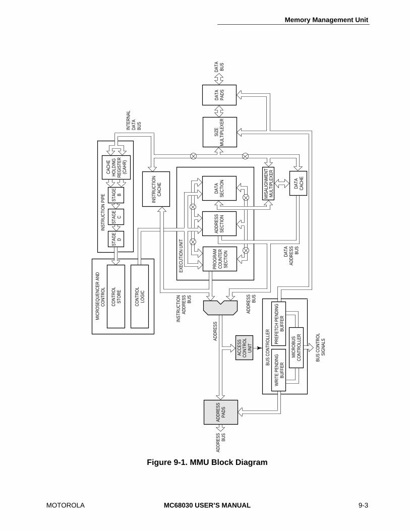
Memory Management Unit
MOTOROLA
MC68030 USER’S MANUAL
9-3
Figure 9-1. MMU Block Diagram
MIC
RO
SEQ
UEN
CER
AN
DC
ON
TRO
L
CO
NTR
OL
STO
RE
INST
RU
CTI
ON
CAC
HE
STAG
EB
STAG
EC
STAG
ED
INTE
RN
ALD
ATA
BUS
INST
RU
CTI
ON
PIP
E
INST
RU
CTI
ON
ADD
RES
SBU
S
ADD
RES
SSE
CTI
ON
PRO
GR
AMC
OU
NTE
RSE
CTI
ON
DAT
ASE
CTI
ON
EXEC
UTI
ON
UN
IT
MIS
ALIG
NM
ENT
MU
LTIP
LEXE
R
SIZE
MU
LTIP
LEXE
RD
ATA
PAD
SD
ATA
BUS
WR
ITE
PEN
DIN
GBU
FFER
PREF
ETC
H P
END
ING
BUFF
ER
MIC
RO
BUS
CO
NTR
OLL
ER
BUS
CO
NTR
OLL
ER
BUS
CO
NTR
OL
SIG
NAL
S
ADD
RES
SBU
S
ADD
RES
SPA
DS
ADD
RES
SBU
S
ADD
RES
S
DAT
AC
ACH
E
DAT
AAD
DR
ESS
BUS
CAC
HE
HO
LDIN
GR
EGIS
TER
(CAH
R)
ACC
ESS
CO
NTR
OL
UN
IT
CO
NTR
OL
LOG
IC
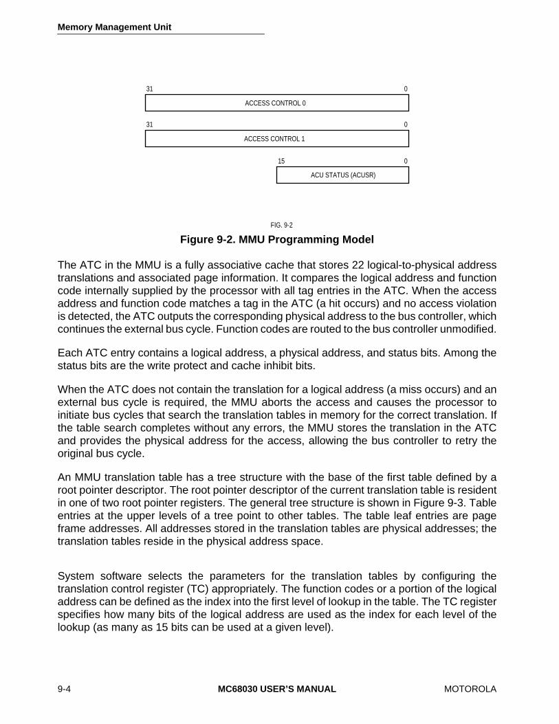
Memory Management Unit
9-4
MC68030 USER’S MANUAL
MOTOROLA
The ATC in the MMU is a fully associative cache that stores 22 logical-to-physical addresstranslations and associated page information. It compares the logical address and functioncode internally supplied by the processor with all tag entries in the ATC. When the accessaddress and function code matches a tag in the ATC (a hit occurs) and no access violationis detected, the ATC outputs the corresponding physical address to the bus controller, whichcontinues the external bus cycle. Function codes are routed to the bus controller unmodified.
Each ATC entry contains a logical address, a physical address, and status bits. Among thestatus bits are the write protect and cache inhibit bits.
When the ATC does not contain the translation for a logical address (a miss occurs) and anexternal bus cycle is required, the MMU aborts the access and causes the processor toinitiate bus cycles that search the translation tables in memory for the correct translation. Ifthe table search completes without any errors, the MMU stores the translation in the ATCand provides the physical address for the access, allowing the bus controller to retry theoriginal bus cycle.
An MMU translation table has a tree structure with the base of the first table defined by aroot pointer descriptor. The root pointer descriptor of the current translation table is residentin one of two root pointer registers. The general tree structure is shown in Figure 9-3. Tableentries at the upper levels of a tree point to other tables. The table leaf entries are pageframe addresses. All addresses stored in the translation tables are physical addresses; thetranslation tables reside in the physical address space.
System software selects the parameters for the translation tables by configuring thetranslation control register (TC) appropriately. The function codes or a portion of the logicaladdress can be defined as the index into the first level of lookup in the table. The TC registerspecifies how many bits of the logical address are used as the index for each level of thelookup (as many as 15 bits can be used at a given level).
Figure 9-2. MMU Programming ModelFIG. 9-2
ACCESS CONTROL 0
31 0
ACCESS CONTROL 1
31 0
ACU STATUS (ACUSR)
15 0

Memory Management Unit
MOTOROLA
MC68030 USER’S MANUAL
9-5
Figure 9-3. Translation Table Tree
ADDRESS BASE ADDRESS MASK
31 24 23 16
E 0 0 0 0 CI R/W RWN 0 FC BASE 0 FC MASK
15 8 7 0
FIG 9-3
ADDRESS BASE - VALUE OF A31-A24 THAT DEFINES BLOCKADDRESS MASK - BITS A31-A24 TO BE IGNORED
E - ENABLE CI - CACHE INHIBIT R/W - READ/WRITE RWM - READ WRITE MASK FC BASE - FUNCTION CODE VALUE FOR BLOCK FC MASK - FUNCTION CODE BITS TO BE IGNORED

Memory Management Unit
9-6
MC68030 USER’S MANUAL
MOTOROLA
9.1 TRANSLATION TABLE STRUCTURE
The M68030 uses the ATC and translation tables stored in memory to perform thetranslation from a logical to a physical address. Translation tables for a program are loadedinto memory by the operating system.
The general translation table structure supported by the MC68030 is a tree structure oftables. The pointer tables form the branches of the tree. These tables contain the baseaddresses of other tables. Page descriptors can reside in pointer tables and, in that case,are called early termination descriptors. The tables at the leaves of the tree are called pagetables. Only a portion of the translation table for the entire logical address space is requiredto be resident in memory at any time: specifically, only the portion of the table that translatesthe logical addresses that the currently executing process(es) use(s) must be resident.Portions of translation tables can be dynamically allocated as the process requiresadditional memory.
As shown in Figure 9-4, the root pointer for a table is a descriptor that contains the baseaddress of the top level table for the tree. The pointer tables and page tables also consist ofdescriptors. A descriptor in a pointer table typically contains the base address of a table atthe next level of the tree. A table descriptor can also contain limits for the index into the nexttable, protection information, and history information pertaining to the descriptor. Each tableis indexed by a field extracted from the logical address. In the example shown in Figure 9-4, the A field of the logical address, $00A, is added to the root pointer value to select adescriptor at the A level of the translation tree. The selected descriptor points to the base ofthe appropriate page table, and the B field of the logical address ($006) is added to this baseaddress to select a descriptor within the page table. A descriptor in a page table containsthe physical base address of the page, protection information, and history information for thepage. A page descriptor can also reside in a pointer table or even in a root pointer to definea contiguous block of pages. A two-level page task is shown. The 32-bit logical addressspace is divided into 4096 segments of 1024 bytes each.
Figure 9-5 shows a possible layout of this example translation tree in memory.
Memory Management Unit
MOTOROLA
MC68030 USER’S MANUAL
9-7
Figure 9-4. Example Translation Table Tree
15 7 0
FIG 9-4
AC - ACCESS CONTROLLED
6 5
AC

Memory Management Unit
9-8
MC68030 USER’S MANUAL
MOTOROLA
9.1.1 Translation Control
The translation control register (TC) defines the size of pages in memory, selects the rootpointer register to be used for supervisor accesses, indicates whether the top level of thetranslation tree is indexed by function code, and specifies the number of logical address bitsused to index into the various levels of the translation tree. The initial shift (IS) field of theTC register defines the size of the logical address space; it contains the number of mostsignificant address bits that are ignored in the translation table lookup. For example, if theIS field is set to zero, the logical address space is 2
32
bytes. On the other hand, if the IS fieldis set to 15, the logical address space contains only 2
32
—2
1
bytes.
The page size (PS) field of the TC register specifies the page size for the system. Thenumber of pages in the system is equal to the logical address space divided by the pagesize. The maximum number of pages that can be defined by a translation tree is greater than16 million (2
32
/2
8
). The minimum number is 4 (2
17
/2
15
). The function code can also be usedin the table lookup, defining as many as seven regions of the above size (FC=0-6). Theentire range of the logical address space(s) can be defined by translation tables of manysizes. The MC68030 provides flexibility that simplifies the implementation of largetranslation tables.
The use of a tree structure with as many as five levels of tables provides granularity intranslation table design. The LIMIT field of the root pointer can limit the value of the firstindex and limits the actual number of descriptors required. Optionally, the top level of thestructure can be indexed by function code bits. In this case, the pointer table at this levelcontains eight descriptors. The next level of the structure (or the top level when the FCL bitof the TC register is set to zero) is indexed by the most significant bits of the logical address(disregarding the number of bits specified by the IS field). The number of logical address bitsused for this index is specified by the TIA field of the TC register. If, for example, the TIAfield contains the value 5, the index for this level contains five bits, and the pointer table atthis level contains at most 32 descriptors.
Similarly, the TIB, TIC, and TID fields of the TC register define the indexes for lower levelsof the translation table tree. When one of these fields contains zero, the remaining TIx fieldsare ignored; the last nonzero TIx field defines the index into the lowest level of the treestructure. The tables selected by the index at this level are page tables; every descriptor inthese tables is (or represents) a page descriptor. Figure 9-6 shows how the TIx fields of theTC register apply to a function code and logical address.
(UNABLE TO LOCATE ART)
Figure 9-5. Example Translation Tree Layout in Memory
(UNABLE TO LOCATE ART)
Figure 9-6. Derivation of Table Index Fields
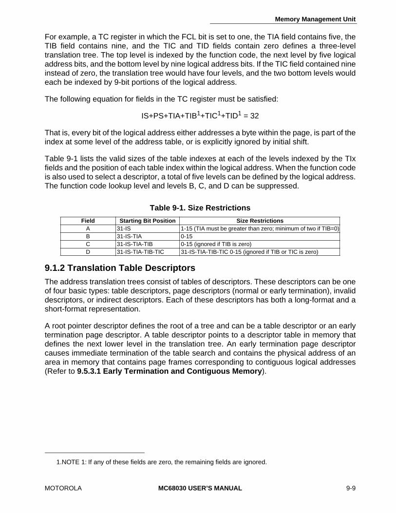
Memory Management Unit
MOTOROLA
MC68030 USER’S MANUAL
9-9
For example, a TC register in which the FCL bit is set to one, the TIA field contains five, theTIB field contains nine, and the TIC and TID fields contain zero defines a three-leveltranslation tree. The top level is indexed by the function code, the next level by five logicaladdress bits, and the bottom level by nine logical address bits. If the TIC field contained nineinstead of zero, the translation tree would have four levels, and the two bottom levels wouldeach be indexed by 9-bit portions of the logical address.
The following equation for fields in the TC register must be satisfied:
IS+PS+TIA+TIB
1
+TIC
1
+TID
1
= 32
That is, every bit of the logical address either addresses a byte within the page, is part of theindex at some level of the address table, or is explicitly ignored by initial shift.
Table 9-1 lists the valid sizes of the table indexes at each of the levels indexed by the TIxfields and the position of each table index within the logical address. When the function codeis also used to select a descriptor, a total of five levels can be defined by the logical address.The function code lookup level and levels B, C, and D can be suppressed.
9.1.2 Translation Table Descriptors
The address translation trees consist of tables of descriptors. These descriptors can be oneof four basic types: table descriptors, page descriptors (normal or early termination), invaliddescriptors, or indirect descriptors. Each of these descriptors has both a long-format and ashort-format representation.
A root pointer descriptor defines the root of a tree and can be a table descriptor or an earlytermination page descriptor. A table descriptor points to a descriptor table in memory thatdefines the next lower level in the translation tree. An early termination page descriptorcauses immediate termination of the table search and contains the physical address of anarea in memory that contains page frames corresponding to contiguous logical addresses(Refer to
9.5.3.1 Early Termination and Contiguous Memory
).
1.NOTE 1: If any of these fields are zero, the remaining fields are ignored.
Table 9-1. Size Restrictions
Field Starting Bit Position Size Restrictions
A 31-IS 1-15 (TIA must be greater than zero; minimum of two if TIB=0)B 31-IS-TIA 0-15C 31-IS-TIA-TIB 0-15 (ignored if TIB is zero)D 31-IS-TIA-TIB-TIC 31-IS-TIA-TIB-TIC 0-15 (ignored if TIB or TIC is zero)
Memory Management Unit
9-10
MC68030 USER’S MANUAL
MOTOROLA
Tables at intermediate levels of a translation tree contain descriptors that are similar to theroot pointer descriptors. They can contain table descriptors or early termination pagedescriptors and can also contain invalid descriptors.
The descriptor tables at the lowest level of a translation tree can only contain pagedescriptors, indirect descriptors, and invalid descriptors. A page descriptor in the lowestlevel of a translation tree defines the physical address of a page frame in memory thatcorresponds to the logical address of a page. An indirect descriptor contains a pointer to theactual page descriptor and can be used when a single page descriptor is accessed by twoor more logical addresses.
To enhance the flexibility of translation table design, descriptors (except for root pointerdescriptors) can be either short or long format. The short-format descriptors consist of onelong word and have no index-limiting capabilities or supervisor-only protection. The long-format descriptors consist of two long words and contain all defined descriptor fields for theMC68030. The pointer and page tables can each contain either short- or long-formatdescriptors, but no single table can contain both sizes. Tables at different levels of thetranslation tree can contain different formats of descriptors. Tables at the same level canalso contain descriptors of different formats, but all descriptors in a particular pointer tableor page table must be of the same format. Figure 9-7 shows a translation tree that usesseveral different format descriptors.
All descriptors contain a descriptor type (DT) field, which identifies the descriptor or specifiesthe size of the descriptors in the table to which the descriptor points. It is always the two leastsignificant bits of the most significant (or only) long word of a descriptor.
Invalid descriptors can be used at any level of the translation tree except the root. When atable search for a normal translation encounters an invalid descriptor, the processor takesa bus error exception. The invalid descriptor can be used to identify either a page or branchof the tree that has been stored on an external device and is not resident in memory or aportion of the translation table that has not yet been defined. In these two cases, theexception routine can either restore the page from disk or add to the translation table.

Memory Management Unit
MOTOROLA
MC68030 USER’S MANUAL
9-11
All long-format descriptors and short-format invalid descriptors include one or two unusedfields. The operating system can use these fields for its own purposes. For example, theoperating system can encode these fields to specify the type of invalid descriptor.Alternately, the external device address of a page that is not resident in main memory canbe stored in the unused field.
9.2 ADDRESS TRANSLATION
The function of the MMU is to translate logical addresses to physical addresses accordingto control information stored by the system in the MMU registers and in translation tabletrees resident in memory.
9.2.1 General Flow for Address Translation
A CPU space address (FC0-FC2=$7) is a special case that is immediately used as aphysical address without translation. For other accesses, the translation process proceedsas follows:
1. Search the on-chip data and instruction caches for the required instruction word or op-erand on read accesses.
2. Compare the logical address and function code to the transparent translation param-eters in the transparent translation registers, and use the logical address as a physical address for the memory access when one or both of the registers match.
3. Compare the logical address and function code to the tag portions of the entries in the ATC and use the corresponding physical address for the memory access when a match occurs.
4. When no on-chip cache hit occurs (on a read) and no TTx register matches or valid ATC entry matches, initiate a table search operation to obtain the corresponding phys-ical address from the corresponding translation tree, create a valid ATC entry for the logical address, and repeat step 3.
Figure 9-8 is a general flowchart for address translation. The top branch of the flowchartapplies to CPU space accesses (FC0-FC2=$7). The next branch applies to read accessesonly. When either of the on-chip caches hits (contains the required data or instruction), nomemory access is necessary. The third branch applies to transparent translation. Thebottom three branches apply to ATC translation as follows. If the requested access missesin the ATC, the memory cycle is aborted, and a table search operation proceeds. An ATCentry is created after the table search, and the access is retried. If an access hits in the ATCbut a bus error was detected during the table search that created the ATC entry, the memoryaccess is aborted, and a bus error exception is taken.
(UNABLE TO LOCATE ART)
Figure 9-7. Example Translation Tree Using Different Format Descriptors
Memory Management Unit
9-12
MC68030 USER’S MANUAL
MOTOROLA
If an access results in an ATC hit but the access is either a write or read-modify-write accessand the page is write protected, the memory cycle is also aborted, and a bus error exceptionis taken. For a write or read-modify-write access, when the modified bit of the ATC entry isnot set, the memory cycle is aborted, a table search proceeds to set the modified bit in boththe page descriptor in memory and in the ATC, and the access is retried. If the modified bitof the ATC entry is set and the bus error bit is not, assuming that neither TTx registermatches and the access is not to CPU space, the ATC provides the address translation tothe bus controller under two conditions: 1) if a read access does not hit in either on-chipcache and 2) if a write or read-modify-write access is not write protected.
The preceding description of the general flowchart specifies several conditions that causethe memory cycle to be aborted. In these cases, the bus cycle is aborted before theassertion of AS.
9.2.2 Effect of RESET On MMU
When the MC68030 is reset by the assertion of the RESET signal, the E bits of the TC andTTx registers are cleared, disabling address translation. This causes logical addresses tobe passed through as physical addresses to the bus controller, allowing an operating systemto set up the translation tables and MMU registers, as required. After it has initialized thetranslation tables and registers, the E bit of the TC register can be set, enabling addresstranslation. A reset of the processor does not invalidate any entries in the ATC. An MMUinstruction (such as PMOVE) that flushes the ATC must be executed to flush all existingvalid entries from the ATC after a reset operation and before translation is enabled.
9.2.3 Effect of MMUDIS On Address Translation
The assertion of MMUDIS prevents the MMU from performing searches of the ATC and theexecution unit from performing table searches. With address translation disabled, logicaladdresses are used as physical addresses. When an initial access to a long-word-aligneddata operand that is larger than the addressed port size is performed, the successive buscycles for additional portions of the operand always use the same higher order address bitsthat were used for the initial bus cycle (changing A0 and A1 appropriately). Thus, if MMUDISis asserted during this type of operation, the disabling of address translation does notbecome effective until the entire transfer is complete. Note that the assertion of MMUDISdoes not affect the operation of the transparent translation registers.
(UNABLE TO LOCATE ART)
Figure 9-8. Address Translation General Flowchart
Memory Management Unit
MOTOROLA
MC68030 USER’S MANUAL
9-13
9.3 TRANSPARENT TRANSLATION
Two independent transparent translation registers (TT0 and TT1) in the MMU optionallydefine two blocks of the logical address space that are directly translated to the physicaladdress spaces. The MMU does not explicitly check write protection for the addresses inthese blocks, but a block can be specified as transparent only for read cycles. The blocks ofaddresses defined by the TTx registers include at least 16M bytes of logical address space;the two blocks can overlap, or they can be separate.
The following description of the address comparison assumes that both TT0 and TT1 areenabled; however, each TTx register can be independently disabled. A disabled TTxregister is completely ignored.
When the MMU receives an address to be translated, the function code and the eight high-order bits of the address are compared to the block of addresses defined by TT0 and TT1.The address space block for each TTx register is defined by the base function code, thefunction code mask, the logical base address, and the logical address mask. When a bit ina mask field is set, the corresponding bit of the base function code or logical base addressis ignored in the function code and address comparison. Setting successively higher orderbits in the address mask increases the size of the transparently translated block.
The address for the current bus cycle and a TTx register address match when the functioncode bits and address bits (not including masked bits) are equal. Each TTx register canspecify read accesses or write accesses as transparent. In that case, the internal read/writesignal must match the R/W bit in the TTx register for the match to occur. The selection ofthe type of access (read or write) can also be masked. The read/write mask bit (RWM) mustbe set for transparent translation of addresses used by instructions that execute read-modify-write operations. Otherwise, neither the read nor write portions of read-modify-writeoperations are mapped transparently with the TTx registers, regardless of the function codeand address bits for the individual cycles within a read-modify-write operation.
Memory Management Unit
9-14
MC68030 USER’S MANUAL
MOTOROLA
By appropriately configuring a transparent translation register, flexible transparent mappingcan be specified. For instance, to transparently translate user program space with a TTxregister, the RWM bit of the register is set to 1, the FC BASE is set to $2, and the FC MASKis set to $0. To transparently translate supervisor data read accesses of addresses$00000000-$0FFFFFFF, the LOGICAL BASE ADDRESS field is set to $0X, the LOGICALADDRESS MASK is set to $0F, the R/W bit is set to 1, the RWM bit is set to 0, the FC BASEis set to $5, and the FC MASK field is set to $0. Since only read cycles are specified by theTTx register for this example, write accesses for this address range can be translated withthe translation tables and write protection can be implemented as required.
Each TTx register can specify that the contents of logical addresses in its block should notbe stored in either an internal or external cache. The cache inhibit out signal (CIOUT) isasserted when an address matches the address specified by a TTx register and the cacheinhibit bit in that TTx register is set. CIOUT is used by the on-chip instruction and datacaches to inhibit caching of data associated with this address. The signal is available toexternal caches for the same purpose.
For an access, if either of these registers match, the access is transparently translated. Ifboth registers match, the CI bits are ORed together to generate the CIOUT signal.
Transparent translation can also be implemented by the translation tables of the translationtrees if the physical addresses of pages are set equal to the logical addresses.
9.4 ADDRESS TRANSLATION CACHE
The ATC is a 22-entry fully associative (content addressable) cache that contains addresstranslations in a form similar to the corresponding page descriptors in memory to providefast address translation of a recently used logical address.
The MC68030 is organized such that the translation time of the ATC is always completelyoverlapped by other operations; thus, no performance penalty is associated with ATCsearches. The address translation occurs in parallel with on-chip instruction and data cacheaccesses before an external bus cycle begins.
Memory Management Unit
MOTOROLA
MC68030 USER’S MANUAL
9-15
If possible, when the ATC stores a new address translation, it replaces an entry that is nolonger valid. When all entries in the ATC are valid, the ATC selects a valid entry to bereplaced, using a pseudo least recently used algorithm. The ATC uses a validity bit and aninternal history bit to implement this replacement algorithm. ATC hit rates are applicationdependent, but hit rates ranging from 98% to greater than 99% can be expected.
Each ATC entry consists of a logical address and information from a corresponding pagedescriptor that contains the physical address. The 28-bit logical (or tag) portion of each entryconsists of three fields:
V — VALIDThis bit indicates the validity of the entry. If V is set, this entry is valid. This bit is set when the MC68030 loads an entry. A flush operation clears the bit. Specifically, any of these operations clear the V bit of an entry:
• A PMOVE instruction with the FD bit equal to zero that loads a value into the CRP, SRP, TC, TT0, or TT1 register.
• A PFLUSHA instruction.
• A PFLUSH instruction that selects this entry.
• A PLOAD instruction for a logical address and FC that matches the tag for this entry. The instruction writes a new entry (with the V bit set) for the specified logical address.
• The selection of this entry for replacement by the replacement algorithm of the ATC.
FC — FUNCTION CODEThis 3-bit field contains the function code bits (FC0-FC2) corresponding to the logical ad-dress in this entry.
LOGICAL ADDRESSThis 24-bit field contains the most significant logical address bits for this entry. All 24 bitsof this field are used in the comparison of this entry to an incoming logical address whenthe page size is 256 bytes. For larger page sizes, the appropriate number of least signifi-cant bits of this field are ignored.
27 26 24 23 0V FC LOGICAL ADDRESS
Memory Management Unit
9-16
MC68030 USER’S MANUAL
MOTOROLA
Each logical portion of an entry has a corresponding 28-bit physical (or data) portion. Thephysical portion contains these fields:
B — BUS ERRORThis bit is set for an entry if a bus error, an invalid descriptor, a supervisor violation, or alimit violation is encountered during the table search corresponding to this entry. When Bis set, a subsequent access to the logical address causes the MC68030 to take a bus er-ror exception. Since an ATC miss causes an immediate retry of the access after the tablesearch operation, the bus error exception is taken on the retry. The B bit remains set untila PFLUSH instruction or a PLOAD instruction for this entry invalidates the entry or untilthe replacement algorithm for the ATC replaces it.
CI — CACHE INHIBITThis bit is set when the cache inhibit bit of the page descriptor corresponding to this entryis set. When the MC68030 accesses the logical address of an entry with the CI bit set, itasserts the cache inhibit out signal (CIOUT) during the corresponding bus cycle. This sig-nal inhibits caching in the on-chip caches and can also be used for external caches.
WP — WRITE PROTECTThis bit is set when a WP bit is set in any of the descriptors encountered during the tablesearch for this entry. Setting a WP bit in a table descriptor write protects all pages access-ed with that descriptor. When the WP bit is set, a write access or a read-modify-write ac-cess to the logical address corresponding to this entry causes a bus error exception to betaken immediately.
M — MODIFIEDThis bit is set when a valid write access to the logical address corresponding to the entryoccurs. If the M bit is clear and a write access to this logical address is attempted, theMC68030 aborts the access and initiates a table search, setting the M bit in the page de-scriptor, invalidating the old ATC entry, and creating a new entry with the M bit set. TheMMU then allows the original write access to be performed. This assures that the firstwrite operation to a page sets the M bit in both the ATC and the page descriptor in thetranslation tables even when a previous read operation to the page had created an entryfor that page in the ATC with the M bit clear.
27 26 25 24 23 0B CI WP M PHYSICAL ADDRESS
Memory Management Unit
MOTOROLA
MC68030 USER’S MANUAL
9-17
PHYSICAL ADDRESSThis 24-bit field contains the physical address bits (A31-A8) from the page descriptor cor-responding to the logical address. When the page size is larger than 256 bytes, not all bitsin the physical address field are used. All page index bits of the logical address are trans-ferred to the bus controller without translation.
9.5 TRANSLATION TABLE DETAILS
The details of translation tables and their use include detailed descriptions of thedescriptors, table searching, translation table structure variations, and the protectiontechniques available with the MC68030 MMU.
9.5.1 Descriptor Details
The descriptor details include detailed descriptions of the short- and long-format descriptorsused in the translation trees. The fields that apply to all descriptors are described in the firstparagraph.
9.5.1.1 DESCRIPTOR FIELD DEFINITIONS.
All descriptor fields are used in more thanone type of descriptor. This section lists these fields and describes the use of each field.
DTThis 2-bit field contains the descriptor type; the first two types apply to the descriptor it-self. The other two types apply to the descriptors in the table at the next level of the tree.The values are defined as follows:
$0 INVALIDThis code identifies the current descriptor as an invalid descriptor. A table search ends when an invalid descriptor is encountered.
$1 PAGE DESCRIPTORThis code identifies the current descriptor as a page descriptor. The page descrip-tor is a normal page descriptor when it resides in a page table (in the bottom level of the translation tree). A page descriptor at a higher level is an early termination page descriptor. A table search ends when a page descriptor of either type is en-countered.
Memory Management Unit
9-18
MC68030 USER’S MANUAL
MOTOROLA
$2 VALID 4 BYTEThis code specifies that the next table to be accessed contains short-format de-scriptors. The MC68030 multiplies the index for the next table by four to access the next descriptor. (Short-format descriptors must be long-word aligned.) When used in a page table (bottom level of an translation tree), this code identifies an indirect descriptor that points to a short-format page descriptor.
$3 VALID 8 BYTEThis code specifies that the next table to be accessed contains long-format de-scriptors. The MC68030 multiplies the index for the next table by eight to access the next descriptor. (Long-format descriptors must be quad-word aligned.) When used in a page table (bottom level of an address translation tree), this code identi-fies an indirect descriptor that points to a long-format page descriptor.
UThis bit is automatically set by the processor when a descriptor is accessed in which theU bit is clear except after a supervisor violation is detected. In a page descriptor table, thisbit is set to indicate that the page corresponding to the descriptor has been accessed. Ina pointer table, this bit is set to indicate that the pointer has been accessed by theMC68030 as part of a table search. Note that a pointer may be fetched, and its U bit set,for an address to which access is denied at another level of the tree. Updates of the U bitare performed before the MC68030 allows a page to be accessed. The processor neverclears this bit.
WPThis bit provides write protection. The states of all WP bits encountered during a tablesearch are logically ORed, and the result is copied to the ATC entry at the end of a tablesearch for a logical address. During a table search for a PTEST instruction, the processorcopies this result into the MMU status register (MMUSR). When WP is set, the MC68030does not allow the logical address space mapped by that descriptor to be written by anyprogram (i.e., this protection is absolute). If the WP bit is clear, the MC68030 allows writeaccesses using this descriptor (unless access is restricted at some other level of the trans-lation tree).
CIThis bit is set to inhibit caching of items within this page by the on-chip instruction and datacaches and, also, to cause the assertion of the CIOUT signal by the MC68030 for bus cy-cles accessing items within this page.
Memory Management Unit
MOTOROLA
MC68030 USER’S MANUAL
9-19
L/UThis bit specifies the type of limit in the LIMIT field. When the L/U bit is set, the LIMIT fieldcontains the unsigned lower limit; the index value for the next level of the tree must begreater than or equal to the value in the LIMIT field. When the bit is cleared, the limit is anunsigned upper limit, and the index value must be less than or equal to the LIMIT. An out-of-bounds access causes the B bit in the ATC entry for the address to be set and causesthe table search to abort.
LIMITThis 15-bit field contains a limit to which the index portion of an address is compared todetect an out-of-bounds index. The limit check applies to the index into the table at thenext lower level of the translation tree. If the descriptor is an early termination page de-scriptor, the limit field is still used as a check on the next index field of the logical address.
MThis bit identifies a modified page. The MC68030 sets the M bit in the corresponding pagedescriptor before a write operation to a page for which the M bit is zero, except after adescriptor with the WP bit set is encountered, or after a supervisor violation is encoun-tered. An access is considered to be a write for updating purposes if either the R/W orRMC signal is low. The MC68030 never clears this bit.
PAGE ADDRESS This 24-bit field contains the physical base address of a page in memory. The low-orderbits of the address are supplied by the logical address. When the page size is larger than256 bytes, one or more of the least significant bits of this field are not used. The numberof unused bits is equal to the PS field value in the TC register minus eight.
SThis bit identifies a pointer table or a page as a supervisor only table or page. When theS bit is set, only programs operating at the supervisor privilege level are allowed to accessthe portion of the logical address mapped by this descriptor. If this bit is clear, accessesusing this descriptor are not restricted to supervisor-only unless the access is restrictedby some other level of the translation tree.
TABLE ADDRESSThis 28-bit field contains the physical base address of a table of descriptors. The low-or-der bits of the address are supplied by the logical address.
Memory Management Unit
9-20
MC68030 USER’S MANUAL
MOTOROLA
DESCRIPTOR ADDRESSThis 30-bit field, which contains the physical address of a page descriptor, is only used inshort- and long-format indirect descriptors.
UNUSEDThe bits in this field are not used by the MC68030 and may be used by the system soft-ware.
RESERVEDDescriptor fields designated by a one or a zero are reserved by Motorola for future defini-tion. These bits should be consistently written as either a one or a zero as appropriate. Inthe root pointers, these bits are not alterable. In memory-resident descriptors, the valuesin these fields are neither checked nor altered by the MC68030. Use of these bits by sys-tem software for any purpose may not be supported in future products.
9.5.1.2 ROOT POINTER DESCRIPTOR.
A root pointer descriptor contains the address ofthe top-level pointer table of a translation tree. This type of descriptor is loaded into the CRPand SRP registers with the PMOVE instruction. The field descriptions in the precedingsection apply to corresponding fields of the CRP and SRP with two minor exceptions. Adescriptor-type code of $00 (invalid) is not allowed; an attempt to load zero into the DT fieldof the CRP or SRP register results in an MMU configuration exception. Also, when the FCLfield of the TC register is set, the L/U and LIMIT fields of the root pointer registers areunused. Figure 9-9 shows the root pointer descriptor format.
9.5.1.3 SHORT-FORMAT TABLE DESCRIPTOR.
The field descriptions in
9.5.1.1DESCRIPTOR FIELD DEFINITIONS
apply to corresponding fields of this descriptor. Figure9-10 shows the format of the short-format table descriptor.
9.5.1.4 LONG-FOMAT TABLE DESCRIPTOR.
The field descriptions in
9.5.1.1DESCRIPTOR FIELD DEFINITIONS
apply to corresponding fields of this descriptor. Duringaddress computations, the MC68030 internally replaces the UNUSED field with zeros.Figure 9-11 shows the format of the long-format table descriptor.
(UNABLE TO LOCATE ART)
Figure 9-9. Root Pointer Descriptor Format
(UNABLE TO LOCATE ART)
Figure 9-10. Short-Format Table Descriptor
(UNABLE TO LOCATE ART)
Figure 9-11. Long-Format Table Descriptor
Memory Management Unit
MOTOROLA
MC68030 USER’S MANUAL
9-21
9.5.1.5 SHORT-FORMAT EARLY TERMINATION PAGE DESCRIPTOR.
The short-format early termination page descriptor contains the page descriptor code in the DT fieldbut resides in a pointer table. That is, the table in which an early termination page descriptoris located is not at the bottom level of the address translation tree. The field descriptions in
9.5.1.1 Descriptor Field Definitions
apply to corresponding fields of this descriptor. Figure9-12 shows the format of the short-format early termination page descriptor.
9.5.1.6 LONG-FORMAT EARLY TERMINATION PAGE DESCRIPTOR.
The long-formatearly termination page descriptor contains the page descriptor code in the DT field butresides in a pointer table like the short-format early termination page descriptor. The fielddescriptions in
9.5.1.1 Descriptor Field Definitions
apply to corresponding fields of thisdescriptor. Figure 9-13 shows the format of the long-format early termination pagedescriptor. The LIMIT field of the long-format descriptor provides a means of limiting thenumber of pages to which the descriptor applies.
(UNABLE TO LOCATE ART)
Figure 9-12. Short-Format Page Descriptor andShort-Format Early Termination Page Descriptor
(UNABLE TO LOCATE ART)
Figure 9-13. Long-Format Early Termination Page Descriptor
Memory Management Unit
9-22
MC68030 USER’S MANUAL
MOTOROLA
9.5.1.7 SHORT-FORMAT PAGE DESCRIPTOR. The short-format page descriptor is usedin the page tables (the bottom level of the address table). The field descriptions in 9.5.1.1Descriptor Field Definitions apply to the corresponding fields of this descriptor. The short-format page descriptor is identical to of the short-format early termination page descriptorshown in Figure 9-12.
9.5.1.8 LONG-FORMAT PAGE DESCRIPTOR. The long-format page descriptor is alsoused in the page tables. The field descriptions in 9.5.1.1 Descriptor Field Definitions applyto the corresponding fields of this descriptor. Figure 9-14 shows the format of the long-format page descriptor.
9.5.1.9 SHORT-FORMAT INVALID DESCRIPTOR. The short-format invalid descriptorconsists of a DT field that contains zeros, identifying it as an invalid descriptor. It can be usedat any level of the address translation tree except at the root pointer level. The 30-bit unusedfield is available to the operating system to identify unallocated portions of the table orportions of the table that reside on an external device. For example, the disk address of disk-resident tables or pages can be stored in this field. Figure 9-15 shows the format of a short-format invalid descriptor.
(UNABLE TO LOCATE ART)
Figure 9-14. Long-Format Page Descriptor
(UNABLE TO LOCATE ART)
Figure 9-15. Short-Format Invalid Descriptor
Memory Management Unit
MOTOROLA MC68030 USER’S MANUAL 9-23
9.5.1.10 LONG-FORMAT INDIRECT DESCRIPTOR. The long-format invalid descriptor isused in pointer and page tables that contain long-format descriptors. It is used in the sameway as the short-format invalid descriptor in the preceding section. The first long wordcontains the DT field in the lowest order bits. The second long word is an unused field, alsoavailable to the operating system. Figure 9-16 shows the format of the long-format invaliddescriptor.
9.5.1.11 SHORT-FORMAT INDIRECT DESCRIPTOR. The short-format indirect descriptordoes not have a unique descriptor-type code. Rather, it resides in a page table (the bottomlevel of the address translation tree) that contains short-format descriptors and is neither apage descriptor nor an invalid descriptor. The descriptor-type field contains either the codefor a valid 4-byte descriptor or for a valid 8-byte descriptor, depending upon the size of thereferenced page descriptor. The field descriptions in 9.5.1.1 Descriptor Field Definitionsapply to the corresponding fields of this descriptor. Figure 9-17 shows the format of a short-format indirect descriptor.
(UNABLE TO LOCATE ART)
Figure 9-16. Long-Format Invalid Descriptor
(UNABLE TO LOCATE ART)
Figure 9-17. Short-Format Indirect Descriptor
Memory Management Unit
9-24 MC68030 USER’S MANUAL MOTOROLA
9.5.1.12 LONG-FORMAT INDIRECT DESCRIPTOR. The long-format indirect descriptorhas all the attributes of the short-format indirect descriptor described in the precedingsection. The only differences are that it is used in a page table that contains long-formatdescriptors and that it has two unused fields. The field descriptions in 9.5.1.1 DescriptorField Definitions apply to corresponding fields of this descriptor. Figure 9-18 shows theformat of a long-format indirect descriptor.
9.5.2 General Table SearchWhen the ATC does not contain a descriptor for the logical address of a processor accessand a translation is required, the MC68030 searches the translation tables in memory andobtains the physical address and status information for the page corresponding to the logicaladdress. When a table search is required, the CPU suspends instruction execution activityand, at the end of a successful table search, stores the address mapping in the ATC andretries the access. The access then results in a match (it hits) and the translated address istransferred to the bus controller (provided no exceptions were encountered).
The table search begins by selecting the translation tree, using function code bit FC2 andthe SRE bit of the TC register, as shown in Table 9-2. SRE is set to enable the supervisorroot pointer, and FC2 is set for supervisor-level accesses. The translation tree with its rootdefined by the SRP register is selected only when SRE and FC2 are both set. Otherwise,the translation table with its root defined by the CRP register is selected. A simplifiedflowchart of the table search procedure is shown in Figure 9-19.
(UNABLE TO LOCATE ART)
Figure 9-18. Long-Format Indirect Descriptor
Memory Management Unit
MOTOROLA MC68030 USER’S MANUAL 9-25
The table search procedure uses physical addresses to access the translation tables. Theread-modify-write (RMC) signal is asserted on the first bus cycle of the search and remainsasserted throughout, ensuring that the entire table search completes without interruption.
The first bus cycle of the search uses the table address field of the appropriate root pointeras the base address of the first table. The low-order bits of the address are supplied by thelogical address. The table is indexed by either the function code or the set of logical addressbits defined by the TIA field of the TC register. The FCL field of the TC register determineswhether or not the function code is used. In either case, the descriptor-type field of the rootpointer selects the scale factor (or multiplier) for the index.
The first access obtains a descriptor. If the descriptor is a table descriptor, the MC68030again accesses memory. The next access uses the table address in the descriptor as thebase address for the next table. The low-order bits of the address are supplied by the logicaladdress. The table is indexed by a set of bits from the logical address using a scale factordetermined by the descriptor type code in the descriptor. If the first table access used thefunction code, the second access uses the bits selected by the TIA field of the TC register.Otherwise, the second access uses the bits selected by the TIB field.
Additional accesses are performed, using the logical address bits specified in TIB, TIC, orTID in order, until an access obtains a page descriptor or an invalid descriptor or until a limitviolation occurs. At this point, whether or not all levels of the address table have beenaccessed, the table search is over. The page descriptor contains the physical address andother information needed for the ATC entry; the MC68030 creates the ATC entry and retriesthe original bus access.
Figure 9-20 shows a table search using the function code and all four TIx fields.
(UNABLE TO LOCATE ART)
Figure 9-19. Simplified Table Search Flowchart
Table 9-2. Translation Tree Selection
FC2 SRE Translation Table Root Pointer0 0 CRP0 1 CRP1 0 CRP1 1 SRP

Memory Management Unit
9-26 MC68030 USER’S MANUAL MOTOROLA
The MC68030 enforces a limit on the index value for the next level of a table search whenlong-format descriptors are used.
The root pointer includes a limit field that applies when the function code lookup is not used(the FCL bit of the TC register is zero). The index used to access the next level table iscompared to the contents of the limit field. The limit field effectively reduces the portion ofthe address space to which a descriptor applies and also reduces the size of the translationtable. The index must reside within the range defined by the limit field. The limit can be alower limit or an upper limit, according to the L/U bit value. When the L/U bit is set, the limitis a lower limit, and an index less than the limit is out of bounds. When the L/U bit is zero,the limit is an upper limit, and an index greater than the limit is out of bounds. The limit fieldis effectively disabled if L/U is set and the limit field contains zero or if L/U is clear and thelimit field contains $7FFF.
During a table search for an normal translation or a PLOAD instruction, if a limit violation isdetected, the ATC is loaded with an entry having the bus error (B) bit set. If a limit violationis detected during a table search for a PTEST instruction, the invalid (I) and limit (L) bits areset in the MMUSR.
During a table search, the U bit in each descriptor that is encountered is checked and set ifit is not already set. Similarly, when the table search is for a write access and the M bit ofthe page descriptor is clear, the processor sets the bit if the table search does not encountera set WP bit or a supervisor violation. Since the read-modify-write (RMC) signal is assertedthroughout the entire table search operation, the read and write operations to update thehistory bits are guaranteed to be uninterrupted.
A table search terminates successfully when a page descriptor is encountered. Theoccurrence of an invalid descriptor, a limit violation, or a bus error also terminates a tablesearch, and the MC68030 takes an exception on the retry of the cycle because of theseconditions. The exception routine should distinguish between anticipated conditions andtrue error conditions. The routine can correct an invalid descriptor that indicates anonresident page or one that identifies a portion of the translation table yet to be allocated.A limit violation or a bus error due to a system malfunction may result in an error messageand termination of the task.
(UNABLE TO LOCATE ART)
Figure 9-20. Five-Level Table Search
Memory Management Unit
MOTOROLA MC68030 USER’S MANUAL 9-27
9.5.3 Variations in Translation Table StructureMany aspects of the MMU translation tree structure are software configurable, allowing thesystem designer flexibility to optimize the performance of the MMU for a particular system.The following paragraphs discuss the variations of the tree structure from the generalstructure discussed previously.
9.5.3.1 EARLY TERMINATION AND CONTIGUOUS MEMORY. The MMU provides theability to map a contiguous range of the logical address space (an integral number of logicalpages) to an equivalent contiguous physical address range with a single descriptor. This isdone by placing the code for page descriptor ($1) in the descriptor type (DT) field of adescriptor at a level of the tree that would normally contain a table pointer, thereby deletinga subtree of the table.
The table search ends when the search encounters a page descriptor, whether or not thepage descriptor is in a page descriptor table at the lowest level of the translation tree.
Termination of the table search by a page descriptor in a pointer descriptor table (i.e., theMC68030 has not encountered a TIx field of zero) is called an early termination. Theterminating page descriptor is called an early termination page descriptor.
An early termination page descriptor takes the place of many page descriptors in atranslation table. It applies to all pages that would exist on the branch on which thedescriptor has been placed, and on any branches from that branch. An early terminationpage descriptor can be used where contiguous pages in physical memory correspond tocontiguous logical pages. If an early termination page descriptor is a long format, the limitfield is applied to the next index field of the logical address. This allows the number of pagesmapped contiguously to be restricted. Refer to 9.1.2 Translation Table Descriptors foradditional information.
If n low-order bits of the logical page address are unused when a page descriptor encodingis encountered, the single descriptor creates a mapping of a contiguous region of the logicaladdress space starting at the logical page address (with n unused bits set to zero) to acontiguous region in the physical address space starting at the page frame base addresswith a size of 2PS+n bytes.
Memory Management Unit
9-28 MC68030 USER’S MANUAL MOTOROLA
When a search is made for a logical address to which an early termination page descriptorapplies, the MC68030 creates an entry in the ATC for the logical address; the physicaladdress in the ATC entry is the sum of the page address field in the descriptor plus an offset.The offset is the logical address with the bits used in the search set to zero.
Although the early termination page descriptor creates a contiguous logical-to-physicalmapping without having to maintain individual descriptors in the translation tree for eachpage that is a member of the contiguous region, the ATC contains one entry for each pagemapped. These entries are created internally each time a page boundary (as determined bythe page size) is crossed in the contiguous region. Figure 9-21 shows an exampletranslation table with a portion of the logical address space translated as a contiguous block.
Note that the DT field can be set to page descriptor at any level of the translation treeincluding the root pointer level. Setting the DT field of a root pointer to page descriptorcreates a direct mapping from the logical to the physical address space with a constantoffset as determined by the value in the table address field of the root pointer.
9.5.3.2 INDIRECTION. The MC68030 provides the ability to replace an entry in a page tablewith a pointer to an alternate entry. The indirection capability allows multiple tasks to sharea physical page while maintaining only a single set of history information for the page (i.e.,the "modified" indication is maintained only in the single descriptor). The indirectioncapability also allows the page frame to appear at arbitrarily different addresses in the logicaladdress spaces of each task.
Using the indirection capability, single entries or entire tables can be shared betweenmultiple tasks. Figure 9-22 shows two tasks sharing a page using indirect descriptors.
When the MC68030 has completed a normal table search (has exhausted all index fields ofthe logical page address), it examines the descriptor-type field of the last entry fetched fromthe translation tables. If the DT field contains a "valid long" ($2) or "valid short" ($3)encoding, this indicates that the address contained in the highest order 30 bits of the tableaddress field of the descriptor is a pointer to the page descriptor that is to be used to mapthe logical address. The processor then fetches the page descriptor of the indicated formatfrom this address and uses the page address field of the page descriptor as the physicalmapping for the logical address.
Memory Management Unit
MOTOROLA MC68030 USER’S MANUAL 9-29
(UNABLE TO LOCATE ART)
Figure 9-21. Example Translation Tree Using Contiguous Memory
Memory Management Unit
9-30 MC68030 USER’S MANUAL MOTOROLA
The page descriptor located at the address given by the indirect descriptor must not have aDT field with a long or short encoding (it must either be a page descriptor or invalid).Otherwise, the descriptor is treated as invalid, and the MC68030 creates an ATC entry withan error condition signaled (bit set).
9.5.3.3 TABLE SHARING BETWEEN TASKS . A page or pointer table can be sharedbetween tasks by placing a pointer to the shared table in the address translation tables ofmore than one task. The upper (nonshared) tables can contain different settings ofprotection bits allowing different tasks to use the area with different permissions. In Figure9-23 two tasks share the memory translated by the table at the B level. Note that task "A"cannot write to the shaded area. Task "B", however, has the WP bit clear in its pointer to theshared table; thus, it can read and write the shared area. Also note that the shared areaappears at different logical addresses for each task.
9.5.3.4 PAGING OF TABLES. It is not required that the entire address translation tree foran active task be resident in main memory at once. In the same way that only the workingset of pages must reside in main memory, only the tables that describe the resident set ofpages need be available in main memory. This paging of tables is implemented by placingthe "invalid" code ($0) in the DT field of the table descriptor that points to the absent table(s).When a task attempts to use an address that would be translated by an absent table, theMC68030 is unable to locate a translation and takes a bus error exception when theexecution unit retries the bus cycle that caused the table search to be initiated.
It is the responsibility of the system software to determine that the invalid code in thedescriptor corresponds to nonresident tables. This determination can be facilitated by usingthe unused bits in the descriptor to store status information concerning the invalid encoding.When the MC68030 encounters an invalid descriptor, it makes no interpretation (ormodification) of any fields of this descriptor other than the DT field, allowing the operatingsystem to store system-defined information in the remaining bits. Typical information that isstored includes the reason for the invalid encoding (tables paged-out, region not allocated,. . .etc.) and possibly the disk address for nonresident tables.
Figure 9-24 shows an address translation table in which only a single page table (table n) isresident and all other page tables are not resident.
(UNABLE TO LOCATE ART)
Figure 9-22. Example Translation Tree Using Indirect Descriptors
Memory Management Unit
MOTOROLA MC68030 USER’S MANUAL 9-31
(UNABLE TO LOCATE ART)
Figure 9-23. Example Translation Tree Using Shared Tables

Memory Management Unit
9-32 MC68030 USER’S MANUAL MOTOROLA
9.5.3.5 DYNAMIC ALLOCATION OF TABLES. Similar to the case of paged tables, it is notrequired that a complete translation tree exist for an active task. The translation tree can bedynamically allocated by the operating system based on requests for access to particularareas.
As in the case of demand paging, it is difficult, if not impossible, to predict the areas ofmemory that are used by a task over any extended period of time. Instead of attempting topredict the requirements of the task, the operating system performs no action for a task untila demand is made requesting access to a previously unused area or an area that is nolonger resident in memory. This same technique can be used to efficiently create atranslation tree for a task.
For example, consider an operating system that is preparing the system to execute apreviously unexecuted task that has no translation tree. Rather than guessing what thememory usage requirements of the task are, the operating system creates a translation treefor the task that maps one page corresponding to the initial value of the program counter forthat task, and possibly, one page corresponding to the initial stack pointer of the task. Allother branches of the translation tree for this task remain unallocated until the task requestsaccess to the areas mapped by these branches. This technique allows the operating systemto construct a minimal translation tree for each task, conserving physical memory utilizationand minimizing operating system overhead.
9.5.4 Detail of Table Search OperationsThe table search operations described in this section are shown in detail in Figures 9-25-9-29.
(UNABLE TO LOCATE ART)
Figure 9-24. Example Translation Tree with Nonresident Tables

Memory Management Unit
MOTOROLA MC68030 USER’S MANUAL 9-33
(UNABLE TO LOCATE ART)
Figure 9-25. Detailed Flowchart of MMU Table Search Operation
Memory Management Unit
9-34 MC68030 USER’S MANUAL MOTOROLA
(UNABLE TO LOCATE ART)
Figure 9-26. Table Search Initialization Flowchart
(UNABLE TO LOCATE ART)
Figure 9-27. ATC Entry Creation Flowchart

Memory Management Unit
MOTOROLA MC68030 USER’S MANUAL 9-35
9.5.5 ProtectionM68000 Family processors provide an indication of the context in which they are operatingon a cycle-by-cycle basis by means of the function code signals. These signals identifyaccesses to the user program space, the user data space, the supervisor program space,and the supervisor data space. The function code signals can be used for protectionmechanisms by setting the function code lookup (FCL) bit in the translation control (TC)register.
The MC68030 MMU provides the capability for separate translation trees for supervisor anduser spaces to be used. When the supervisor root pointer enable bit (SRE) in the TC registeris set, the root pointer register for the supervisor space translation tree is selected forsupervisor program or data accesses.
The translation table trees contain both mapping and protection information. Each table andpage descriptor includes a write-protect (WP) bit, which can be set to provide writeprotection at any level. Each long-format table and page descriptor also contains asupervisor-only (S) bit, which can limit access to programs operating at the supervisorprivilege level.
(UNABLE TO LOCATE ART)
Figure 9-28. Limit Check Procedure Flowchart
Memory Management Unit
9-36 MC68030 USER’S MANUAL MOTOROLA
The protection mechanisms can be used individually or in any combination to protect:
• Supervisor program and data spaces from access by user programs.
• User program and data spaces from access by other user programs or supervisor pro-grams (except with the MOVES instruction).
• Supervisor and user program spaces from write accesses (except by the supervisor us-ing the MOVES instruction).
• One or more pages of memory from write accesses.
9.5.5.1 FUNCTION CODE LOOKUP. One way of protecting supervisor and user spacesfrom unauthorized access is to set the FCL bit in the TC register. This effectively segmentsthe logical address space into a supervisor program space, a supervisor data space, a userprogram space, and a user data space, as shown in Figure 9-30. Each task has an addresstranslation tree with unique mappings for the logical addresses in its user spaces. Thetranslation tables for mapping the supervisor spaces can be copied into each task'stranslation tree. Figure 9-31 shows a translation tree using function code lookup, and Figure9-32 shows translation trees for two tasks that share common supervisor spaces.
(UNABLE TO LOCATE ART)
Figure 9-29. Detailed Flowchart of Descriptor Fetch Operation
(UNABLE TO LOCATE ART)
Figure 9-30. Logical Address Map Using Function Code Lookup

Memory Management Unit
MOTOROLA MC68030 USER’S MANUAL 9-37
(UNABLE TO LOCATE ART)
Figure 9-31. Example Translation Tree Using Function Code Lookup

Memory Management Unit
9-38 MC68030 USER’S MANUAL MOTOROLA
9.5.5.2 SUPERVISOR TRANSLATION TREE. A second protection mechanism uses asupervisor translation tree. A supervisor translation tree protects supervisor programs anddata from access by user programs and user programs and data from access by supervisorprograms. Access is granted to the supervisor programs which can access any area ofmemory with the move address space (MOVES) instruction. When the SRE bit in the TCregister is set, the translation tree pointed to by the SRP is selected for all supervisor levelaccesses. This translation tree can be common to all tasks. This technique segments thelogical address space into user and supervisor areas without adding the function code levelto the translation trees.
9.5.5.3 SUPERVISOR ONLY. A third mechanism protects supervisor programs and datawithout segmenting the logical address space into supervisor and user address spaces. Thelong formats of table descriptors and page descriptors contain S bits to protect areas ofmemory from access by user programs. When a table search for a user access encountersan S bit set in any table or page descriptor, the table search is completed and an ATCdescriptor corresponding to the logical address is created with the B bit set. The subsequentretry of the user access results in a bus error exception being taken. The S bit can be usedto protect the entire area of memory defined in a branch of the translation tree or only oneor more pages from user program access.
9.5.5.4 WRITE PROTECT. The MC68030 provides write protection independently of thesegmented address spaces for programs and data. All table and page descriptors containWP bits to protect areas of memory from write accesses of any kind. When a table searchencounters a WP bit set in any table or page descriptor, the table search is completed andan ATC descriptor corresponding to the logical address is created with the WP bit set. Thesubsequent retry of the write access results in a bus error exception being taken. The WPbit can be used to protect the entire area of memory defined in a branch of the translationtree, or only one or more pages from write accesses. Figure 9-33 shows a memory map ofthe logical address space organized to use S and WP bits for protection. Figure 9-34 showsan example translation tree for this technique.
(UNABLE TO LOCATE ART)
Figure 9-32. Example Translation Tree Structure for Two Tasks

Memory Management Unit
MOTOROLA MC68030 USER’S MANUAL 9-39
(UNABLE TO LOCATE ART)
Figure 9-33. Exmple Logical Address Map with Shared Supervisor and User Address Spaces

Memory Management Unit
9-40 MC68030 USER’S MANUAL MOTOROLA
(UNABLE TO LOCATE ART)
Figure 9-34. Exmple Translation Tree Using S and WP Bits to Set Protection
Memory Management Unit
MOTOROLA MC68030 USER’S MANUAL 9-41
9.6 MC68030 AND MC68851 MMU DIFFERENCESThe MC68851 paged memory management unit provides memory management for theMC68020 as a coprocessor. The on-chip MMU of the MC68030 provides many of thefeatures of the MC68020/MC68851 combination. The following functions of the MC68851are not available in the MC68030 MMU:
• Access Levels
• Breakpoint Registers
• Root Pointer Table
• Aliases for Tasks
• Lockable Entries in the ATC
• ATC Entries Defined as Shared Globally
In addition, the following features of the MC68030 MMU differ from the MC68020/MC68851pair:
• 22-Entry ATC
• Reduced Instruction Set
• Only Control-Alterable Addressing Modes Supported for MMU Instructions
In general, the MC68030 is program compatible with the MC68020/MC68851 combination.However, in a program for the MC68030, the following instructions must be avoided oremulated in the exception routine for F-line unimplemented instructions: PVALID,PFLUSHR, PFLUSHS, PBcc, PDBcc, PScc, PTRAPcc, PSAVE, PRESTORE, and PMOVEfor unsupported registers (CAL, VAL, SCC, BAD, BACx, DRP, and AC). Additionally, theeffective addressing modes supported on the MC68851 that are not emulated by theMC68030 must be simulated or avoided.

Memory Management Unit
9-42 MC68030 USER’S MANUAL MOTOROLA
9.7 REGISTERSThe registers of the MMU described here are part of the supervisor programming model forthe MC68030.
The six registers that control and provide status information for address translation in theMC68030 are the CPU root pointer register (CRP), the supervisor root pointer register(SRP), the translation control register (TC), two independent transparent translation controlregisters (TT0 and TT1), and the MMU status register (MMUSR). These registers can beaccessed directly by programs that execute only at the supervisor level.
9.7.1 Root Pointer RegistersThe supervisor root pointer (SRP), used for supervisor accesses only, is enabled or disabledin software. The CPU root pointer (CRP) corresponds to the current translation table for userspace (when the SRP is enabled) or for both user and supervisor space (when the SRP isdisabled). The CRP is a 64-bit[lz register that contains the address and related statusinformation of the root of the translation table tree for the current task. When a new taskbegins execution, the operating system typically writes a new root pointer descriptor to theCRP. A new translation table address implies that the contents of the address translationcache (ATC) may no longer be valid. Therefore, the instruction that loads the CRP canoptionally flush the ATC.
The SRP is a 64-bit register that optionally contains the address and related statusinformation of the root of the translation table for supervisor area accesses. The SRP is usedwhen operating at the supervisor privilege level only when the supervisor root pointer enablebit (SRE) of the translation control register (TC) is set. The instruction that loads the SRPcan optionally flush the ATC. The format of the CRP and SRP is shown in Figure 9-35 anddefines the following fields:
Lower/Upper (L/U)Specifies that the value contained in the limit field is to be used as the unsigned lower limit of indexes into the translation tables when this bit is set. When this bit is cleared, the limit field is the unsigned upper limit of the translation table indexes.
Memory Management Unit
MOTOROLA MC68030 USER’S MANUAL 9-43
LimitSpecifies a maximum or minimum value for the index to be used at the next level of tablesearch (the function code level cannot be limited). To suppress the limit function, the L/Ubit is cleared and the limit field is set to ones ($7FFF in the word containing both fields),or the L/U bit is set and the limit field is cleared ($8000 in that word).
Descriptor Type (DT)Specifies the type of descriptor contained in either the root pointer or in the first level ofthe translation table identified by the root pointer. The values are:
$0 INVALIDThis value is not allowed at the root pointer level. When a root pointer register is loaded with an invalid root pointer descriptor, an MMU configuration exception is taken.
$1 PAGE DESCRIPTORA translation table for this root pointer does not exist. The MC68030 internally cal-culates an ATC entry (page descriptor) for accesses using this root pointer within the current page by adding (unsigned) the value in the table address field to the incoming logical address. This results in direct mapping with a constant offset (the table address). For this case, the processor performs a limit check, regardless of the state of the FCL bit in the TC register.
$2 VALID 4 BYTEThe translation table at the root of the translation tree contains short-format de-scriptors. The MC68030 must scale the table index for this level of the table search by 4 bytes to access the next descriptor.
$3 VALID 8 BYTEThe translation table at the root of the translation tree contains long-format de-scriptors. The MC68030 must scale the table index for this level of the table search by 8 bytes to access the next descriptor.
Table AddressContains the physical base address (in bits 31-4) of the translation table at the root pointer level. When the DT field contains $1, the value in the table address field is the offset used to calculate the physical address for the page descriptor. The table addressfield can contain zero (for zero offset).
UnusedBits 3-0 of the root pointer are not used and are ignored when written. All other unusedbits must always be zeros.
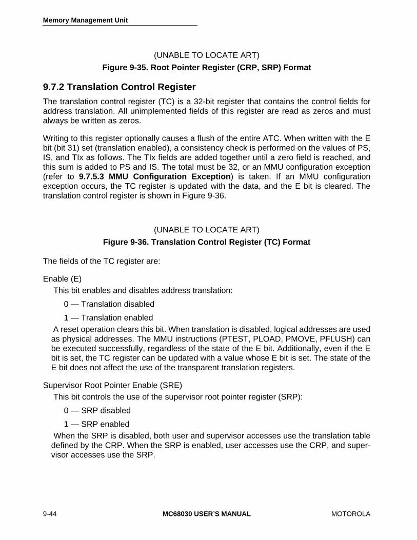
Memory Management Unit
9-44 MC68030 USER’S MANUAL MOTOROLA
9.7.2 Translation Control RegisterThe translation control register (TC) is a 32-bit register that contains the control fields foraddress translation. All unimplemented fields of this register are read as zeros and mustalways be written as zeros.
Writing to this register optionally causes a flush of the entire ATC. When written with the Ebit (bit 31) set (translation enabled), a consistency check is performed on the values of PS,IS, and TIx as follows. The TIx fields are added together until a zero field is reached, andthis sum is added to PS and IS. The total must be 32, or an MMU configuration exception(refer to 9.7.5.3 MMU Configuration Exception) is taken. If an MMU configurationexception occurs, the TC register is updated with the data, and the E bit is cleared. Thetranslation control register is shown in Figure 9-36.
The fields of the TC register are:
Enable (E) This bit enables and disables address translation:
0 — Translation disabled
1 — Translation enabled A reset operation clears this bit. When translation is disabled, logical addresses are usedas physical addresses. The MMU instructions (PTEST, PLOAD, PMOVE, PFLUSH) canbe executed successfully, regardless of the state of the E bit. Additionally, even if the Ebit is set, the TC register can be updated with a value whose E bit is set. The state of theE bit does not affect the use of the transparent translation registers.
Supervisor Root Pointer Enable (SRE) This bit controls the use of the supervisor root pointer register (SRP):
0 — SRP disabled
1 — SRP enabled When the SRP is disabled, both user and supervisor accesses use the translation tabledefined by the CRP. When the SRP is enabled, user accesses use the CRP, and super-visor accesses use the SRP.
(UNABLE TO LOCATE ART)
Figure 9-35. Root Pointer Register (CRP, SRP) Format
(UNABLE TO LOCATE ART)
Figure 9-36. Translation Control Register (TC) Format
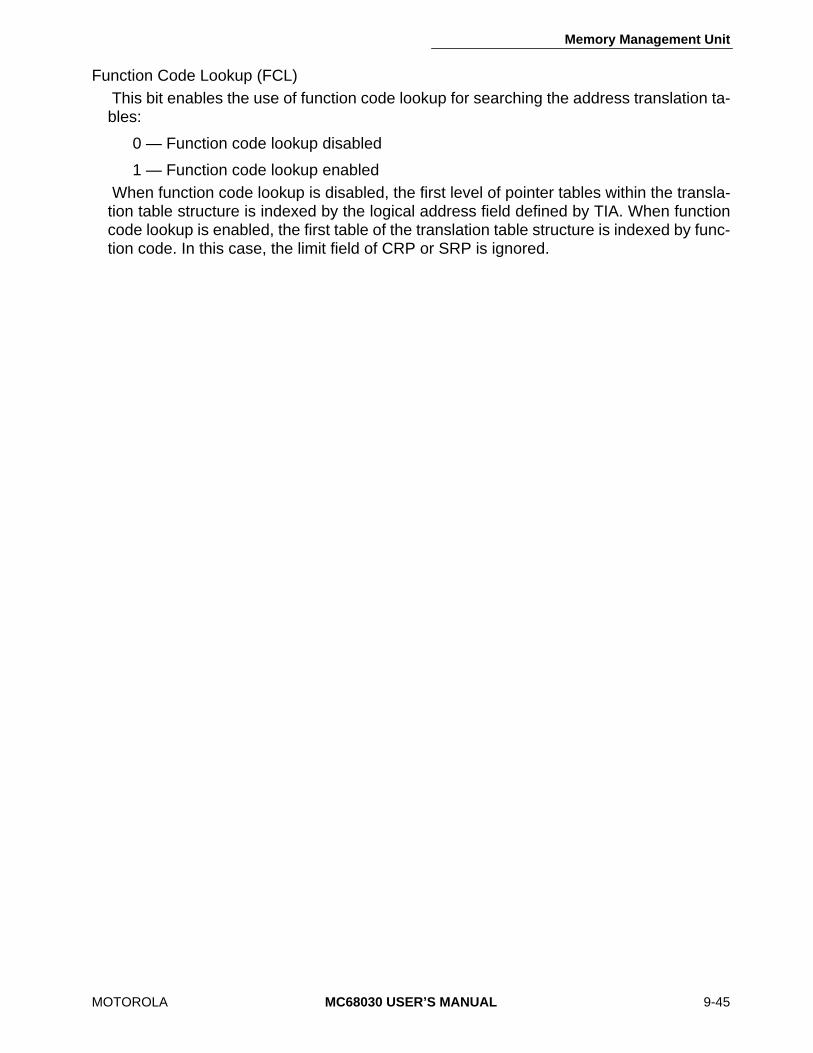
Memory Management Unit
MOTOROLA MC68030 USER’S MANUAL 9-45
Function Code Lookup (FCL) This bit enables the use of function code lookup for searching the address translation ta-bles:
0 — Function code lookup disabled
1 — Function code lookup enabled When function code lookup is disabled, the first level of pointer tables within the transla-tion table structure is indexed by the logical address field defined by TIA. When functioncode lookup is enabled, the first table of the translation table structure is indexed by func-tion code. In this case, the limit field of CRP or SRP is ignored.
Memory Management Unit
9-46 MC68030 USER’S MANUAL MOTOROLA
Page Size (PS) This 4-bit field specifies the system page size:
1000 — 256 bytes 1001 — 512 bytes 1010 — 1K bytes 1011 — 2K bytes 1100 — 4K bytes 1101 — 8K bytes 1110 — 16K bytes 1111 — 32K bytes
All other bit combinations are reserved by Motorola for future use; an attempt to load oth-er values into this field of the TC register causes an MMU configuration exception.
Initial Shift (IS)This 4-bit field contains the number of high-order bits of the logical address that are ig-nored during table search operations. The field contains an integer, 0-15, which sets theeffective size of the logical address to 32-17 bits, respectively. Since all 32 bits of the ad-dress are compared during address translation, bits ignored due to initial shift cannot haverandom values. They must be specified and be consistent with the translation table valuesin order to ensure that subsequent address translations match the corresponding entriesin the ATC.
Table Index (TIA, TIB, TIC, and TID)These 4-bit fields specify the numbers of logical address bits used as the indexes for thefour possible levels of the translation tables (not including the optional level indexed bythe function codes). The index into the highest level table (following the function code,when used) is specified by TIA, and the lowest level, by TID. The fields contain integers,0-15. When a zero value in a TIx field is encountered during a table search operation, thesearch is over unless the indexed descriptor is a table (indirect) descriptor.
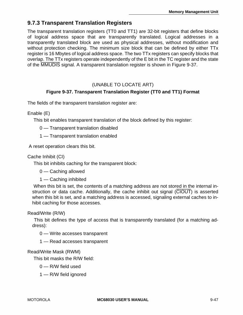
Memory Management Unit
MOTOROLA MC68030 USER’S MANUAL 9-47
9.7.3 Transparent Translation RegistersThe transparent translation registers (TT0 and TT1) are 32-bit registers that define blocksof logical address space that are transparently translated. Logical addresses in atransparently translated block are used as physical addresses, without modification andwithout protection checking. The minimum size block that can be defined by either TTxregister is 16 Mbytes of logical address space. The two TTx registers can specify blocks thatoverlap. The TTx registers operate independently of the E bit in the TC register and the stateof the MMUDIS signal. A transparent translation register is shown in Figure 9-37.
The fields of the transparent translation register are:
Enable (E) This bit enables transparent translation of the block defined by this register:
0 — Transparent translation disabled
1 — Transparent translation enabled
A reset operation clears this bit.
Cache Inhibit (CI) This bit inhibits caching for the transparent block:
0 — Caching allowed
1 — Caching inhibited When this bit is set, the contents of a matching address are not stored in the internal in-struction or data cache. Additionally, the cache inhibit out signal (CIOUT) is assertedwhen this bit is set, and a matching address is accessed, signaling external caches to in-hibit caching for those accesses.
Read/Write (R/W) This bit defines the type of access that is transparently translated (for a matching ad-dress):
0 — Write accesses transparent
1 — Read accesses transparent
Read/Write Mask (RWM) This bit masks the R/W field:
0 — R/W field used
1 — R/W field ignored
(UNABLE TO LOCATE ART)
Figure 9-37. Transparent Translation Register (TT0 and TT1) Format
Memory Management Unit
9-48 MC68030 USER’S MANUAL MOTOROLA
When RWM is set to one, both read and write accesses of a matching address are trans-parently translated. For transparent translation of read-modify-write cycles with matchingaddresses, RWM must be set to one. If the RWM bit equals zero, neither the read nor thewrite of any read-modify-write cycle is transparently translated with the TTx register.
Function Code Base (FC BASE)This 3-bit field defines the base function code for accesses to be transparently translatedwith this register. Addresses with function codes that match the FC BASE field (and areotherwise eligible) are transparently translated.
Function Code Mask (FC MASK)This 3-bit field contains a mask for the FC BASE field. Setting a bit in this field causes the corresponding bit of the FC BASE field to be ignored.
LOGICAL ADDRESS BASEThis 8-bit field is compared with address bits A31-A24. Addresses that match in this comparison (and are otherwise eligible) are transparently translated.

Memory Management Unit
MOTOROLA MC68030 USER’S MANUAL 9-49
LOGICAL ADDRESS MASKThis 8-bit field contains a mask for the LOGICAL ADDRESS BASE field. Setting a bit inthis field causes the corresponding bit of the LOGICAL ADDRESS BASE field to be ig-nored. Blocks of memory larger than 16 Mbytes can be transparently translated by settingsome of the logical address mask bits to ones. Normally, the low-order bits of this field areset to define contiguous blocks larger than 16 Mbytes, although this is not required.
9.7.4 MMU Status RegisterThe MMU status register (MMUSR) is a 16-bit register that contains the status informationreturned by execution of the PTEST instruction. The PTEST instruction searches either theATC (PTEST with level 0) or the translation tables (PTEST with levels of 1-7) to determinestatus information about the translation of a specified logical address. The MMUSR is shownin Figure 9-38.
(UNABLE TO LOCATE ART)
Figure 9-38. MMU Status Register (MMUSR) Format
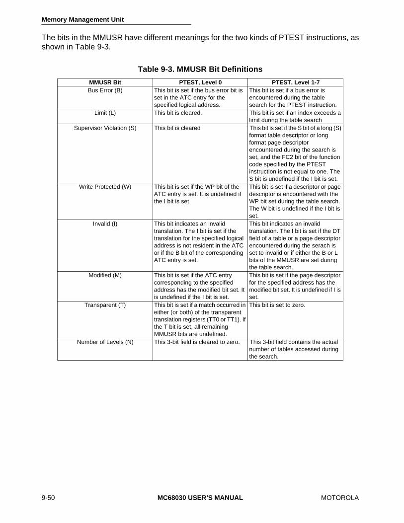
Memory Management Unit
9-50 MC68030 USER’S MANUAL MOTOROLA
The bits in the MMUSR have different meanings for the two kinds of PTEST instructions, asshown in Table 9-3.
Table 9-3. MMUSR Bit Definitions
MMUSR Bit PTEST, Level 0 PTEST, Level 1-7Bus Error (B) This bit is set if the bus error bit is
set in the ATC entry for the specified logical address.
This bit is set if a bus error is encountered during the table search for the PTEST instruction.
Limit (L) This bit is cleared. This bit is set if an index exceeds a limit during the table search
Supervisor Violation (S) This bit is cleared This bit is set if the S bit of a long (S) format table descriptor or long format page descriptor encountered during the search is set, and the FC2 bit of the function code specified by the PTEST instruction is not equal to one. The S bit is undefined if the I bit is set.
Write Protected (W) This bit is set if the WP bit of the ATC entry is set. It is undefined if the I bit is set
This bit is set if a descriptor or page descriptor is encountered with the WP bit set during the table search. The W bit is undefined if the I bit is set.
Invalid (I) This bit indicates an invalid translation. The I bit is set if the translation for the specified logical address is not resident in the ATC or if the B bit of the corresponding ATC entry is set.
This bit indicates an invalid translation. The I bit is set if the DT field of a table or a page descriptor encountered during the serach is set to invalid or if either the B or L bits of the MMUSR are set during the table search.
Modified (M) This bit is set if the ATC entry corresponding to the specified address has the modified bit set. It is undefined if the I bit is set.
This bit is set if the page descriptor for the specified address has the modified bit set. It is undefined if I is set.
Transparent (T) This bit is set if a match occurred in either (or both) of the transparent translation registers (TT0 or TT1). If the T bit is set, all remaining MMUSR bits are undefined.
This bit is set to zero.
Number of Levels (N) This 3-bit field is cleared to zero. This 3-bit field contains the actual number of tables accessed during the search.
Memory Management Unit
MOTOROLA MC68030 USER’S MANUAL 9-51
9.7.5 Register Programming ConsiderationsIf the entries in the address translation cache (ATC) are no longer valid when a resetoperation occurs, an explicit flush operation must be specified by the software. Theassertion of RESET disables translations by clearing the E bits of the TC and TTx registers,but it does not flush the ATC. Flushing of the ATC is optional under control of the FD bit ofthe PMOVE instruction that loads a new value into the SRP, CRP, TT0, TT1, or TC register.
The programmer of the MMU must be aware of effects resulting from loading certainregisters. A subsequent section describes these effects. The MMUSR values lendthemselves to the use of a case structure for branching to appropriate routines in a bus errorhandler. An example of a flowchart that implements this technique is shown in anothersection. A third section describes the conditions that result in MMU exceptions.
9.7.5.1 REGISTER SIDE EFFECTS. The PMOVE instruction is used to load or read any ofthe MMU registers (CRP, SRP, TC, MMUSR, TT0, and TT1). Since loading the rootpointers, the translation control register, or the transparent translation registers with newvalues can cause some or all of the address translations to change, it may be desired toflush the ATC of its contents any time these registers are written. The opcodes of thePMOVE instructions that write to CRP, SRP, TC, TT0, and TT1 contain a flush disable (FD)bit that optionally flushes the ATC when these instructions are executed. If the FD bit equalsone, the ATC is not flushed when the instruction is executed. If the FD bit equals zero, theATC is flushed during the execution of the PMOVE instruction.
9.7.5.2 MMU STATUS REGISTER DECODING. The seven status bits in the MMU statusregister (MMUSR) indicate conditions to which the operating system should respond. In atypical bus error handler routine, the flows shown in Figures 9-39 and 9-40 can be used todetermine the cause of an MMU fault. The PTEST instructions set the bits in the MMUSRappropriately, and the program can branch to the appropriate code segment for thecondition. Figure 9-39 shows the flow for a PTEST instruction for the ATC (level 0), andFigure 9-40 shows the flow for a PTEST instruction that accesses an address translationtree (levels 1-7).
Memory Management Unit
9-52 MC68030 USER’S MANUAL MOTOROLA
9.7.5.3 MMU CONFIGURATION EXCEPTION. The exception vector table in the MC68030assigns a vector for an MMU configuration error exception. The configuration exceptionoccurs as the result of loading invalid data into the TC, SRP, or CRP register.
When the TC register is loaded with the E bit set, the MMU performs a consistency checkof the values in all the four bit fields. The values in the TIx fields are added until the first zerois encountered. The values in the PS and IS fields are added to the sum of the TIx fields. Ifthe sum is not equal to 32, the PMOVE instruction causes an MMU configuration exception.The instruction also causes a configuration exception when a reserved value ($0-$7) isplaced in the PS field of the TC register.
A PMOVE instruction that loads either the CRP or the SRP causes an MMU configurationexception if the new value of the DT field is zero (invalid). In this case, the register is loadedwith the new value before the exception is taken.
(UNABLE TO LOCATE ART)
Figure 9-39. MMU Status Interpretation PTEST Level 0

Memory Management Unit
MOTOROLA MC68030 USER’S MANUAL 9-53
9.8 MMU INSTRUCTIONSThe MC68030 instruction set includes four privileged instructions that perform MMUoperations. A brief description of each of these instructions follows.
The PMOVE instruction transfers data between a CPU register or memory location and anyone of the six MMU registers. The operating system uses the PMOVE instruction to controland monitor MMU operation by manipulating and reading these registers. Optionally, aPMOVE instruction flushes the ATC when it loads a value into the TC, SRP, CRP, TT0, orTT1 register.
(UNABLE TO LOCATE ART)
Figure 9-40. MMU Status Interpretation PTEST Level 7

Memory Management Unit
9-54 MC68030 USER’S MANUAL MOTOROLA
The PFLUSH instruction flushes (invalidates) address translation descriptors in the ATC.PFLUSHA, a version of the PFLUSH instruction, flushes all entries. The PFLUSH instructionflushes all entries with a specified function code or the entry with a specified function codeand logical address.
The PLOAD instruction performs a table search operation for a specified function code andlogical address and then loads the translation for the address into the ATC. The operatingsystem can use this instruction to initialize the ATC to minimize table searching duringprogram execution. Any existing entry in the ATC that translates the specified address isflushed. The preload can be executed for either read or write attributes. If the write attributeis selected (PLOADW), the MC68030 performs the table search and updates all historyinformation in the translation tables (used and modified bits) as if a write operation to thataddress had occurred. Similarly, if the read attribute is selected (PLOADR), the historyinformation in the translation table (used bit) is updated as if a read operation had occurred.The PLOAD instruction does not alter the MMUSR.
The PTEST instruction either searches the ATC or performs a table search operation for aspecified function code and logical address, and sets the appropriate bits in the MMUSR toindicate conditions encountered during the search. The physical address of the lastdescriptor fetched can be returned in an address register. The exception routines of theoperating system can use this instruction to identify MMU faults. The PTEST instructiondoes not alter the ATC.
This instruction is primarily used in bus error handling routines. For example, if a bus errorhas occurred, the handler can execute an instruction such as:
PTESTW #1,([A7, offset]),#7,A0
This instruction requests that the MC68030 search the translation tables for an address inuser data space (#1) and examine protection information. This particular logical address isobtained from the exception stack frame ([A7, offset]). The MC68030 is instructed to searchto the bottom of the table (#7 — there cannot be more than six levels) and return the physicaladdress of the last table entry used in register A0. After executing this instruction, thehandler can examine the MMUSR for the source of the fault and use A0 to access the lastdescriptor. Note that the PTESTR and PTESTW instructions have identical results exceptfor PTEST0 when either TTx register matches the logical address and the R/W bit of thatregister is not masked.
The MMU instructions use the same opcodes and coprocessor identification (CpID) as thecorresponding instructions of the MC68851. All F-line instructions with CpID=0 (includingMC68851 instructions) that the MC68030 does not support automatically cause F-lineunimplemented instruction exceptions when their execution is attempted in the supervisemode. If execution of a unimplemented F-line instruction with CpID=0 is attempted in theuser mode, the MC68030 takes a privilege violation exception. F-line instructions with aCpID other than zero are executed as coprocessor instructions by the MC68030.

Memory Management Unit
MOTOROLA MC68030 USER’S MANUAL 9-55
9.9 DEFINING AND USING PAGE TABLES IN AN OPERATING SYSTEMMany factors must be considered when determining how to use the MMU in an operatingsystem. The MC68030 provides the flexibility required to optimize an operating system formany system implementations. The example operating system described in the next sectionpresents one approach to operating system design, with many of the tradeoffs discussed.
9.9.1 Root Pointer RegistersAn operating system can use the CPU root pointer (CRP) register alone or both the CRPand the supervisor root pointer (SRP) registers to point to the top level address translationtable(s). The choice depends on the complexity of the memory layout for the system. Whenonly the CRP is used, it must point to a translation table that maps all supervisor and userreferences. However, the supervisor and user translation tables can be separate even whenonly the CRP register is used. When the index to the top level translation table is the functioncode value (FCL in TC register is set), supervisor and user tables are separate at all lowerlevels. With proper structuring of the address tables, both methods can provide the samefunctionality, but each has its advantages.
When the translation tables use the CRP and function code lookup, supervisor and useraccesses are separate, and each task can have different supervisor and user mappings.Alternatively, the entries in the function code tables that correspond to the supervisor spacesfor each task can all point to the same tables to provide a common mapping for all supervisorreferences.
When the mapping of the supervisor address space is identical for all tasks, the SRP can beused in conjunction with the CRP to provide a more simple and efficient way to define themapping. This technique suppresses the use of the function code (unless the program anddata spaces require distinct mappings) and separates supervisor and user accesses at theroot pointer level of the translation tables. A single translation table maps all supervisoraccesses without maintaining a large number of supervisor pointers in the translation tablesfor each task, resulting in reduced bus activity for table searches.
Memory Management Unit
9-56 MC68030 USER’S MANUAL MOTOROLA
9.9.2 Task Memory Map DefinitionThe MC68030 provides several different means by which the supervisor can access theuser address spaces. The supervisor can access any user address, regardless of how thevirtual space is partitioned, with the MOVES (move space) instruction. Some systemsprovide a complete 4-Gbyte virtual memory map for each task. Indeed, an operating systemthat runs other operating systems in a virtual machine environment must provide a completemap to accurately emulate the full addressing range for the subordinate operating system.
With the large address space of the MC68030, each individual user task or all user taskscan share the address space with the operating system. One method of performing thisfunction is implemented in the example operating system in the next section. Sharing theaddress space provides direct access to user data items by the operating system. Anotheradvantage of this mapping method is that tasks can easily share code. Common routinessuch as file I/O handlers and arithmetic conversion packages can be written re-entrantly andbe restricted to read-only access from all user tasks in the system.
The simplest example of a shared virtual address space system is one in which each userand supervisor process is given a unique virtual address range within the single 4-Gbytevirtual address space. In other words, the system has only one linear virtual address space;all processes run somewhere in that space. Only one translation table tree is required forthe entire system, but each task can have individual tables if desired. With the common treeapproach, the operating system can access any item of any task without modifying the rootpointer. Otherwise, only the currently active task is immediately accessible, which often isadequate. To switch tasks, the operating system only has to update the user program anduser data pointers in the highest level translation table indexed by the function code. Thisgives each task access to its own data only. This scheme has the advantages of simple tablemanagement and easy sharing of common items by giving them the same virtual addressfor all tasks in the system. This scheme might be ideal for real-time systems that do notrequire more complexity in memory management facilities.
Memory Management Unit
MOTOROLA MC68030 USER’S MANUAL 9-57
The next logical step toward increased operating system complexity, with shared user andsupervisor virtual memory maps, is to keep the supervisor addresses separate but to giveeach user task its own use of the remainder of the virtual space. For example, each usertask could have the virtual memory space from zero to 512 Mbytes; the operating systemprograms and data would occupy the remainder of the space, from 512 Mbytes up to 4Gbytes. Each user task has its own set of translation tables. The supervisor root pointer mayor may not be used, depending on whether the user tables also map the supervisor space.As in the preceding method, the user cannot access the operating system portion of theaddress space unless the operating system allows it or wishes to share common routines.The advantages of this scheme are that it provides a much larger virtual address space foreach user task and it avoids virtual memory fragmentation problems. Disadvantages of thisscheme include the requirement for slightly more complex table management and therestriction of operating system access to only the current user task.
There are few absolute rules in the use of the MC68030 MMU. In general, the statementregarding restricting operating system access to only one user task using the schemedescribed in the preceding paragraph holds true. However, by using the entire 4-Gbytevirtual address space and cross mapping the address space, the supervisor can accesseach user task space as a distinct portion of its own supervisor map. If each user task islimited to a 16-Mbyte virtual address space and the supervisor only requires a 16-Mbyteaddress space, 256 such address spaces can be mapped simultaneously. The supervisortranslation tables can include each of these spaces, and the supervisor can access eachtask using indexed addressing with a register that contains the proper constant for aparticular task. This constant provides a supervisor-to-user virtual address conversion. Asystems programmer can implement some very sophisticated functions that exploit theflexibility of the MMU.
The most complex systems and those that implement virtual machine capability completelyseparate the virtual address spaces of the supervisor and all user tasks, or possibly eventhose of individual supervisor tasks. Each user or supervisor task has its own virtual memoryspace starting at zero and extending to 4 Gbytes. Using the function code, a 4-Gbyteaddress space for the program and another for its data can be provided for each task. Boththe SRP and the CRP are probably used, since nothing is common among the variousspaces. The operating system uses the MOVES instruction to interact with the user space.The advantages of this implementation are the maximum availability of the virtual space anda complete logical separation of addresses. Virtual machine implementations requiremaximum availability of virtual space. The disadvantages are the more complex tablemanagement and the more restrictive accesses to other address spaces.

Memory Management Unit
9-58 MC68030 USER’S MANUAL MOTOROLA
9.9.3 Impact of MMU Features On Table DefinitionThe features of the MMU that impact table definition are usually considered after decidinghow to map memory for the tasks. For some systems, these features can affect the mappingdecision and should be considered when making that decision.
9.9.3.1 NUMBER OF TABLE LEVELS. The MMU supports from zero to five levels (sixlevels with the use of indirection) in the address translation tables. The zero-level case isearly termination at the root pointer. This provides a limit check on the range of physicaladdresses for the system. It is used primarily in systems that require the limit check onphysical addresses.
Systems that support large page sizes or that require only limited amounts of virtual memoryspace can use single-level tables. A single-level translation tree with 32K-byte pages maybe the best choice for systems that are primarily numerically intensive (i.e., the system isinvolved in arithmetic manipulations rather than data movement) where the overhead ofvirtual page faults and paging I/O must be minimized. This type of system can map a 16-Mbyte address space with only 2K bytes of page table space. With this much mappedaddress space, table search time becomes insignificant.
At another extreme is a single-user business system that only needs a 2-Mbyte[lz virtualaddress space. A 512-byte page size might be best for this system, because the block sizeformats of many Winchester hard disk file systems is 512 bytes. A page table thatcompletely maps the 2-Mbyte space requires only 16K bytes of memory, and the ATCentries directly map 11K bytes of virtual space at any one time. The page tables for thissystem and the one described in the preceding paragraph are small enough to bepermanently allocated in the operating system data area. They incur virtually nomanagement or swapping overhead.
A two-level address translation table provides a lower page level similar to the page tablesin the two preceding paragraphs and additional direction at a higher level. For example, ina system using 32K-byte pages and 512-entry page tables, the upper level translation tablecontains 256 entries of short-format descriptors, requiring 1K bytes for the table. Each of theupper table entries maps a 16-Mbyte region of the virtual address space. The primaryadvantage of a two-level table for large "number-crunching" system is the operating systemdesigner's ability to make a tradeoff between page size and table size. The system designermay choose a smaller page size to fit the block sizes on available I/O devices, yet keep thetables manageable. However, the designer must also consider the performance penaltyassociated with smaller page sizes. Systems with smaller page sizes have a higherfrequency of page faults requiring more table search time and paging I/O. With the flexibilityof the MC68030 MMU, the designer has enough choices to optimize table structure designand page size.

Memory Management Unit
MOTOROLA MC68030 USER’S MANUAL 9-59
Three-level translation tables are useful when the operating system makes heavy use ofshared memory spaces and/or shared page tables. Sophisticated systems often sharetranslation tables or program and data areas defined at the page table level. When a tableentry can point to a translation table also used by a different task, sharing memory areasbecomes efficient. The direct access to user address space by the supervisor is an exampleof sharing memory.
Some artificial intelligence systems require very large virtual address spaces with only smallfragments of memory allocated among these widely differing addresses. This fragmentationis due to the complex and recursive actions the system performs on lists of data. Theseactions require the system to constantly allocate and free sophisticated pointers and linkedlists in the memory map. The fragmentation suggests a small page size to utilize memorymost efficiently. However, small pages in a large virtual memory map require relatively largetranslation tables. For example, to map 4 Gbytes of virtual address space with 256-bytepages, the page tables alone require 64 Mbytes. With a three- or four-level table structure,the number of actual translation table entries can be drastically reduced. The designer canuse invalid descriptors to represent blocks of unused addresses and the limit fields in validdescriptors to minimize the sizes of pointer and page tables. In addition, paging of theaddress tables themselves reduces memory requirements.
9.9.3.2 INITIAL SHIFT COUNT. The initial shift field (IS) of the translation control register(TC) can decrease the size of translation tables. When the required virtual address spacecan be addressed with fewer than 32 bits, the IS field reduces the size of the virtual addressspace by discarding the appropriate number of the most significant logical address bits. Thistechnique inhibits the system's ability to detect very large illegal (i.e., out-of-bounds)addresses. Using the full 32-bit address and reducing the table size with invalid descriptorsand limited pointer and page table sizes prevents this problem.
Memory Management Unit
9-60 MC68030 USER’S MANUAL MOTOROLA
9.9.3.3 LIMIT FIELDS. Except for a table indexed by function code, every pointer and pagetable can have a defined limit on its size. Defining limits provides flexibility in the operatingsystem and saves memory in the translation tables. The limit field of a table descriptor limitsthe size of the table to which it points. The limit can be either an upper or a lower limit, usingeither the lower or higher addresses within the range of the table. Since a task seldomrequires the maximum number of possible virtual pages, this reduction in table size ispractical.
For example, when an operating system uses 4K-byte pages and runs numerous smalltasks that average 80K bytes each in size, each task requires a 20-entry page table. Thesystem can limit the size of each table to 80 bytes, or 800 bytes for ten tasks. Without thelimit, an operating system running ten of these tasks would require 40K bytes of space forthe page tables alone (one table per page).
Memory savings required for translation tables is especially significant for artificialintelligence systems these systems tend to require very large memory maps. By using limitfields, each table is only as large as the number of active entries within it. This limit canchange as the table grows. For higher level tables, each table only grows as the additionalentries require. The use of three or four levels of tables facilitates the management of thesetables.
9.9.3.4 EARLY TERMINATION PAGE DESCRIPTORS. A page descriptor residing in apointer table is an early termination page descriptor mapping an entire block of pages. Thatis, it maps a contiguous range of virtual addresses to a contiguous range of physicaladdresses. For example, an operating system could reserve a 32K-byte area for specialsupervisor I/O peripheral devices. This area can be mapped with a single early terminationdescriptor to save translation table size and table search overhead. The descriptor can usethe limit field to reduce the size of the contiguous block when the block size is smaller thanthe virtual address space that the particular descriptor represents. The MC68030 createsmultiple ATC entries (one for each page) for the range of virtual addresses represented bythe early termination descriptor as the pages are accessed.
Memory Management Unit
MOTOROLA MC68030 USER’S MANUAL 9-61
An operating system can use an early termination page descriptor to map a contiguousblock of memory for each task (both program and data). The tasks can be relocated bychanging the physical address portion of the descriptor. This scheme is useful when thetasks in a system consist of one or a few sequential blocks of memory that can be swappedas a group. The operating system memory map can treat the entire address space withinthese blocks as a uniform virtual space available for all tasks. The system only requires onetranslation table; by the use of limit fields and early termination page descriptors, it mapscomplete segments of memory.
9.9.3.5 INDIRECT DESCRIPTORS. An indirect descriptor is a table descriptor residing in apage table. It points to another page descriptor in the translation tree. Using an indirectdescriptor for a page makes the page common to several tasks. History information for acommon page is maintained in only one descriptor. Access to the page sets the used (U)bit, and a write operation to the page sets the M (modified) bit for that page. When theoperating system is searching for an available page, it simply checks the page tablecontaining the descriptor for the common page to determine its status. With other methodsof page sharing, the system would have to check page tables for all sharing tasks todetermine the status of the common page.
9.9.3.6 USING UNUSED DESCRIPTOR BITS. In general, the bits in the unused fields ofmany types of descriptors are available to the operating system for its own purposes. Theinvalid descriptor, in particular, uses only two bits of the 32 (short) or 64 (long) bits availablewith that format. An operating system typically uses these fields for the software flags,indicating whether the virtual address space is allocated and whether an image resides onthe paging device. Also, these fields often contain the physical address of the image.
The operating system often maintains information in an unused field about a page residentin memory. This information may be an aging counter or some other indication of the page'sfrequency of use. This information helps the operating system to identify the pages that areleast likely to impact system performance if they are reallocated. The system should first usephysical page frames that are not allocated to a virtual page. Next it should use pages withthe longest time since the most recent access. Pages that do not have the M (modified) bitset should be taken first, since they do not need to be copied to the paging device (theexisting image remains valid).

Memory Management Unit
9-62 MC68030 USER’S MANUAL MOTOROLA
An aging counter can be set up in an unused field of a page descriptor. The system canperiodically check the U (used) bit for the page and increment the count when the page hasnot been used since the previous check. The system can identify the least recently usedpage from the counts in the aging counter. When the counter for a page overflows, thesystem can list the page in a queue of least recently used pages from which it chooses thenext page to be reallocated.
Many schemes afford the operating system designer a variety in selecting a page to betaken. One operating system scans page tables, starting at the lowest priority task, lookingfor aged pages to steal. Another system maintains a system-wide list of all page frames asthey are used and scans the list, starting at the oldest, to find a page to steal. A sophisticatedsystem keeps a working set model of active pages for each individual task. From thisinformation, it can swap a complete block of pages in and out with a single I/O operation.The method chosen can have a dramatic impact on limiting page fault overhead in a heavilyused system.
9.10 AN EXAMPLE OF PAGING IMPLEMENTATION IN AN OPERATING SYSTEM
This section describes an example operating system design that illustrates some of theMMU features. The description suggests alternatives to provide variations of the design.Memory management algorithms that can be implemented to derive the actual code areshown. A bus error handler routine is shown also. Implementing the algorithms develops thebasic code for the memory management services of an operating system.
9.10.1 System DescriptionThe example system has the ability to map a large virtual memory task space, which isrequired for execution of predominantly numerically intensive processing tasks. Most ofthese tasks do not need more than 16 Mbytes of memory, but the system can supply a largervirtual memory space (as large as 496 Mbytes) to the occasional task that requires more.The system uses the relatively large page size of 8K bytes to minimize thrashing andtranslation table searches. With a larger page size, fewer descriptors can map a large areaof virtual memory. Also, in a given period of time, the MC68030 experiences fewer ATCmisses and performs fewer table searches. The larger page size requires the paging I/Ooperations to transfer larger blocks of data, and sometimes only a small part of the page isactually used. However, preliminary software model simulations show that 8K-byte pagesprovide optimum performance for this type of processing.
Memory Management Unit
MOTOROLA MC68030 USER’S MANUAL 9-63
The average task for this system is a compiler or text editor that requires only 192K bytes ofmemory, or 24 8K-byte pages. Using short page descriptors, the page table occupies 96bytes.
Page tables can reside at any 16-byte boundary; the limit fields of the MMU can provide thearea needed without requiring excess space. This results in an address table area smallenough to be completely resident in physical memory. The operating system does not needto page the table areas.
The paging hardware of many computer systems requires lower level tables to reside atpage boundaries, effectively using one or more entire pages. This requires 80K bytes for thepage tables for 10 tasks (10 tables, one 8K-byte page per table). Then, when the memoryrequired for an upper level of tables is added, at a minimum of 8K bytes per task, the totalcomes to over 160K bytes. Table base addresses in the MC68030 are zero modulo 16addresses. This results in a dramatic savings of memory for address table space; instead ofusing 80K bytes for the page tables for 10 tasks, (10 tables, one 8K-byte page per table),the MC68030 needs 960 bytes. Instead of 8K bytes per task for the upper level of tables,the tables require 2560 bytes in the MC68030. The fragmentation that may occur inallocating smaller tables could increase the memory requirement but would still remain lessthan 160K bytes.
The translation table tree for the example system consists of two levels. The upper level isa fixed table that contains 32 entries, each of which is a long-format table descriptor thatpoints to a lower level page table. Each page table maps as many as 16 Mbytes of virtualaddress space. Since the upper level table is small (256 bytes), it can easily fit in the maincontrol block of the task. When the system dispatches a new task, it loads a pointer to theupper level table for the task into the CRP register. Each lower level table consists of 0-2048short-format page descriptors. The limit entry in the table descriptor for a page tabledetermines the size of the table. For the average 192K-byte task, the upper level tableusually has one valid entry, and this entry points to a lower level table with an average sizeof 96 bytes. A task that requires more than 16 Mbytes uses more than one valid entry in thehigher level table.
Memory Management Unit
9-64 MC68030 USER’S MANUAL MOTOROLA
In a typical computer system, with 64K bytes of boot and diagnostics ROM, a 64K I/O area,and 1 Mbyte of RAM, the physical mapping appears as follows:
The operating system must control memory allocation for physical memory (page frames)to hold the pages of virtual memory. All available physical memory is divided into pageframes, each of which can hold a page of virtual memory. A system with 4 Mbytes of actualmemory is divided into 512 8K-byte frames that can theoretically hold 512 pages of activevirtual memory at any one time. Usually, operating system components (exception handlers,the kernel, private memory pool) permanently reside in some of the memory. Only theremaining page frames are available for virtual memory pages.
The operating system maintains a linked list of all unallocated page frames. One simple wayto do this is for each unallocated frame to contain a pointer to the next frame. The operatingsystem takes the first page frame on the list when a frame is required. An operating systemprimitive called GetFrame performs this function and returns the physical address of anavailable frame. When all frames are allocated, GetFrame steals a frame from another task.GetFrame first looks for an unmodified frame to steal. An unmodified frame could be stolenwithout waiting for the page to be copied back to the external storage device that storesvirtual page images. (This device is called the paging device or the backing store.) If nounmodified page frame is available, GetFrame must wait while the system copies a modifiedpage to the paging device, then steals the page frame and returns to the caller with thephysical address.
Next, the operating system needs physical memory management routines to allocate andfree supervisor work memory. The routine must allocate pieces of memory on boundariesof at least modulo 16, the requirement for address translation tables. Typically, this type ofroutine allocates pieces of certain sizes. GetReal is the allocation routine; ReturnReal is thereturn routine. They use physical addresses.
With physical memory allocation provided for, the operating system must be able to managevirtual memory for all tasks. To do this, the system must be aware of the virtual memory map.It must know the total amount of virtual memory space, how much is allocated, and whichareas are available to be assigned to tasks. The virtual memory map looks like this:
Virtual addresses for this virtual memory are subdivided:
(UNABLE TO LOCATE ART)
(UNABLE TO LOCATE ART)
(UNABLE TO LOCATE ART)
Memory Management Unit
MOTOROLA MC68030 USER’S MANUAL 9-65
The translation table structure consists of:
CRP → upper level table in the task control block, which contains 32 long pointers:
[0] → lower level table common to all tasks; maps all operating system areas (first 4Mbytes of virtual space). This common table contains 512 short-page entries(2K bytes).
[1] → lower level table for first 16 Mbytes of user program/data/stack area.
• • •
[31] → lower level table for last 16 Mbytes (of 496 total) of user program/data/stackarea.
The user program can only access virtual addresses starting at 16 Mbytes and extendingupward to the limit of 512 Mbytes. The code, the data, and the stacks for user tasks areallocated in this area of virtual memory. Supervisor programs can access the entire virtualmap; they can access addresses that directly access the I/O ports as well as the entirephysical memory at untranslated addresses. The address tables are set up so that virtualaddresses are equal to the physical addresses for the supervisor between 1 and 3 Mbytes.Folding the physical address space into the virtual space greatly simplifies operations thatuse physical addresses. The folding does not necessarily mean that the virtual addressesare the same as the physical addresses. For example, the boot/diagnostic ROM at physicaladdress zero could be assigned a virtual address of 3 Mbytes. However, any external busmasters or circuitry (such as breakpoint registers) resident on the physical side of the busmust have physical addresses. This requires the overhead of operating system code toperform address translation.
This virtual memory map provides supervisor addresses that are unique with respect to useraddresses; all supervisor routines can directly access any user area without being restrictedto certain instructions or addressing modes. The separate user and supervisor mapssuggest that two root pointers should be used, one for the supervisor map and one for theuser map. However, the supervisor must be able to access user translation tables for properaccess to user data items. With separate root pointers, the supervisor table structure mustbe linked to that of the user. To do this requires an additional level of table lookup (functioncode level) for the supervisor address table.
This example uses a simpler scheme instead. Only the CPU root pointer is used, and, foreach task, the first entry of the upper level table (for the supervisor portion, the first 16Mbytes of virtual address space) points to the same lower level table. This common lowerlevel table has supervisor protection and maps the entire virtual operating system, physicalI/O, and physical memory areas. This scheme avoids the requirement for extra lookup levelsor pointer manipulations during a task switch to furnish correct access across the user/supervisor boundary. All the operating system has to do when creating the address table fora new task is to set the first upper level table entry to point to the common page table of thesupervisor.

Memory Management Unit
9-66 MC68030 USER’S MANUAL MOTOROLA
To solve the problem of accounting for virtual memory areas assigned to a user task, theoperating system uses the existing translation tables to identify these areas. When a validdescriptor points to a given virtual address page, this 8K-byte page of memory has beenallocated. This scheme provides areas of memory that are multiples of the 8K-byte pagesize. Due to the 8K granularity, this scheme would be inadequate for tasks that continuallyrequest and return virtual memory space. As a result, some other technique would be used(perhaps auxiliary tables to show virtual space availability). The tasks in this system seldomrequest additional memory space; any request made is for a large area. This schemesuffices. The application programs and utilities that run in the UNIX (r) environment havesimilar requirements for memory.
The operating system primitive GetVirtual allocates virtual memory space for tasks. Theinput parameter is a block size, in bytes; GetVirtual returns the virtual address for the newblock. GetVirtual first checks that the requested size is not too large. Then it scans thetranslation tables looking for an unallocated virtual memory area large enough to hold therequested block. If it does not find enough space, GetVirtual attempts to increase the pagetable size to its maximum. If this does not provide the space, GetVirtual returns an errorindication. When the routine finds enough virtual space for the block, it sets the pagedescriptors for the block to virgin status (invalid, but allocated). When these pages are firstused, a page fault is generated. The operating system allocates a page frame for the pageand replaces the descriptor with a valid page descriptor. The status (indicated by a softwareflag in the invalid descriptor) tells the operating system that the paging device does not havea page image for this page; no read operation from the paging device is required.
When the status of an invalid descriptor indicates that a page image must be read in,primitive SwapInPage, reads in the image. The input parameter for this routine is the invaliddescriptor, which contains the disk address of the page image. Before returning,SwapInPage replaces the invalid descriptor with a valid page descriptor that contains thepage address. The page is now ready for use.
Memory Management Unit
MOTOROLA MC68030 USER’S MANUAL 9-67
These routines provide many of the functions required for the memory managementservices of an operating system, but a complete memory management system requires acomplementary function for each routine. The complementary function usually performs thesame steps in the reverse order. The complement of GetVirtual could be ReturnVirtual; forSwapInPage, the complement might be SwapOutPage. These counterparts can be derivedto perform similar steps in the reverse order.
9.10.2 Allocation RoutinesThis section describes the central routine Vallocate, which user programs call to obtainmemory. In this section (and the next), a loose high-level language syntax is used for thecode. The code takes many liberties to enhance readability. For example, the code assignsdescriptive strings for return status values. These strings typically represent binary values.Also, the code uses empty brackets to represent obvious subscripts in loops that scantables. In such a loop, the subscript on the second line is obvious:
for Upper-Table-Index=1 to 31 do if Upper-Table [Upper-Table-Index].Status=invalid then ...
In the code shown here, the second line is:
if Upper-Table [].Status=invalid then ...
The code uses flag operations that are assumed to be defined elsewhere in the system.They may imply more complex operations than bit manipulations. For example, page tablestatus of invalid virgin can be implemented with an invalid descriptor instead of the pagedescriptor, and a software flag bit in the descriptor that indicates the page is allocated buthas never been used (the paging device has no page image).
Vallocate has a single input parameter, the required memory size in bytes. It returns statusinformation and the virtual address of the start of the area (if the memory is allocated). Tosimplify the routine, it always returns a multiple of the system page size and never allocatesa block that crosses a 16-Mbyte boundary. It could allocate a portion of a page byimplementing a control structure to subdivide a page, but, if the control structure were withinthe allocated page, the user could corrupt it. The block could cross a 16-Mbyte boundary ifthe routine included code to keep track of consecutive free blocks when scanning the lowerlevel tables, each of which represents 16 Mbytes of address space. Once the total area islocated, Vallocate allocates the consecutive blocks and returns the address of the lowestblock.
The 32 upper level table entries are long pointer types; each represents 16 Mbytes of virtualaddress space. Each entry is either invalid (has no lower page tables) or allocated (haslower page tables and a limit field that defines the table size). By convention, the first entrymaps the supervisor address space and has supervisor protection. The routine nevermodifies this first entry. The 31 entries after the first are available to be allocated as useraddress space.
Memory Management Unit
9-68 MC68030 USER’S MANUAL MOTOROLA
A routine similar to this that linearly extends (grows) a previously allocated memory blockcould be written. A stack is a good example. The operating system can allocate the top ofthe memory (the thirty-second upper level table entry) as a stack that grows downward fromthe highest address. If a task needs several large stacks, a 16-Mbyte block can be used foreach stack, with a software flag set to indicate growth in a downward direction.
The logic of Vallocate is:
1. Validate the request and calculate number of pages required.
2. Scan each upper table entry's lower page tables (where they exist) looking for an ad-equate group of unallocated pages.
3. If no space is found, see if the lower table is less than its maximum size and if the block can be allocated by expanding it at the end.
4. If still no space is found, use the next free upper table entry and initialize its new lower level page table to allocate the block here.
5. Set allocated page entries to indicate virgin status (allocated, invalid, and not swapped out).
6. Return status. If status is OK, also return virtual address.
The code for Vallocate is:
9.10.3 Bus Error Handler RoutineThe routine that processes bus error exceptions is the most critical part of the memorymanagement services provided by the example operating system. This routine mustdetermine the validity of page faults and perform the necessary processing. It must identifythe conditions that aborted the executing task. The PTEST instruction can investigate thecause of a bus error by performing a table search using the address and type of access thatproduced the error, accumulating status information during the search.
When the PTEST instruction does not find any error, the bus error was most likely amalfunction (for example, a transient memory failure). The operating system must respondappropriately.
(UNABLE TO LOCATE ART)
(UNABLE TO LOCATE ART)
(UNABLE TO LOCATE ART)
Memory Management Unit
MOTOROLA MC68030 USER’S MANUAL 9-69
The table search performed by the PTEST instruction may end in a bus error termination.Either the address translation tables are not correctly built or main memory has failed (eithera transient or permanent failure).
A supervisor protection violation or a write protection violation usually indicates that the taskgenerating the exception attempted to access an area of the virtual address space that isnot part of the task's address space. The operating system usually recovers from such anerror by terminating (aborting) the task.
When the PTEST instruction returns the invalid status, the bus error is a page fault, and theoperating system must identify the specific type of page fault. When the limit violation bitreturned by the PTEST instruction is set, the task that took the exception was trying toaccess a page that has not been allocated. The example system aborts the task in this case.In other systems, this is an implicit request for more virtual memory, particularly if thereference is in a stack area.
When no limit violation occurred, a descriptor is invalid. Typically, the descriptor containssoftware flags that provide relevant information. The example operating system checks tosee if the invalid descriptor is in an upper level or a lower level table. When the descriptor isin the upper level table, the task was attempting to access unallocated virtual memory, andthe system aborts the task. When the descriptor is in a lower level table, the system checkssoftware flags to identify the invalid descriptor.
When the software flags indicate that the descriptor corresponds to an unallocated page,the system aborts the task. When the descriptor refers to a virgin page (allocated, but notyet accessed) and the request for the page was a read request, the page is actually invalidbecause the read operation reads unknown data. However, the example operating systemdoes not consider the type of request, but assigns a physical page frame to the page andwrites the page descriptor to the page table. Some systems clear virgin pages to zero.

Memory Management Unit
9-70 MC68030 USER’S MANUAL MOTOROLA
When the software flags indicate that the page is allocated and the image has been copiedto the paging device, the operating system assigns a page frame, reads the page image intothe frame, and writes the page descriptor to the page table. Another possible type of invaliddescriptor is one that requires special processing, such as one that refers to a virtual I/Odevice area in a virtual machine.
Obtaining a page frame for a virtual page may be an obvious operation. However, when noidle page frame is available, the system must steal one. If the page in the stolen frame hasbeen modified in memory, the system must save the page image on the paging device. Thesystem must alter the translation table of the task that loses the frame to show that the pageis allocated and swapped out. Typically, the translation table entry shows the address of thepage image on the paging device.
The method a system uses to select a page frame to steal varies a great deal from systemto system. A simple system may just steal a page from the lowest priority task. Moreadvanced systems select the page frame that has not been accessed for the longest time.This process, called aging, is done in several ways. One method uses bits of the pagedescriptor as an aging counter. Periodically, the operating system examines the U (used)bits and increments the count for pages that have not been used. The system maintains alist of pages with aging counters that have overflowed. The pages on this list are availablefor stealing.
Some systems keep a separate list of pages that have not been modified since the pageimage was read from memory. The page frames that contain these pages can be stolenwithout swapping out because the existing page image on the paging device remains valid.
Page stealing software can involve many dynamics of the system. It can consider taskpriority, I/O activity, working-set determinations, the number of executing tasks, a thrashinglevel, and other factors.
Memory Management Unit
9-71 MC68030 USER’S MANUAL MOTOROLA
The example bus error exception routine is called BusErrorHandler. It is more general thanVallocate because it relies on several operating-system-dependent items. The variablepointer VictimTask is assumed to point to a table from a task that is losing a page frame.This assumption is necessary because control block layout and the method of searching forand finding other tasks in the example operating system are not defined. The code is furthersimplified by omitting the function code value and the read/write status, which do not affectthe basic logic of the program.
(UNABLE TO LOCATE ART)
(UNABLE TO LOCATE ART)
(UNABLE TO LOCATE ART)

Memory Management Unit
9-72 MC68030 USER’S MANUAL MOTOROLA
MOTOROLA
MC68030 USER’S MANUAL
10-1
SECTION 10COPROCESSOR INTERFACE DESCRIPTION
The M68000 Family of general-purpose microprocessors provides a level of performancethat satisfies a wide range of computer applications. Special-purpose hardware, however,can often provide a higher level of performance for a specific application. The coprocessorconcept allows the capabilities and performance of a general-purpose processor to beenhanced for a particular application without encumbering the main processor architecture.A coprocessor can efficiently meet specific capability requirements that must typically beimplemented in software by a general-purpose processor. With a general-purpose mainprocessor and the appropriate coprocessor(s), the processing capabilities of a system canbe tailored to a specific application.
The MC68030 supports the M68000 coprocessor interface described in this section. Thesection is intended for designers who are implementing coprocessors to interface with theMC68030.
The designer of a system that uses one or more Motorola coprocessors (the MC68881 orMC68882 floating-point coprocessor, for example) does not require a detailed knowledge ofthe M68000 coprocessor interface. Motorola coprocessors conform to the interfacedescribed in this section. Typically, they implement a subset of the interface, and that subsetis described in the coprocessor user's manual. These coprocessors execute Motoroladefined instructions that are described in the user's manual for each coprocessor.
10.1 INTRODUCTION
The distinction between standard peripheral hardware and a M68000 coprocessor isimportant from a perspective of the programming model. The programming model of themain processor consists of the instruction set, register set, and memory map available to theprogrammer. An M68000 coprocessor is a device or set of devices that communicates withthe main processor through the protocol defined as the M68000 coprocessor interface. Theprogramming model for a coprocessor is different than that for a peripheral device. Acoprocessor adds additional instructions and generally additional registers and data typesto the programming model that are not directly supported by the main processorarchitecture. The additional instructions are dedicated coprocessor instructions that utilizethe coprocessor capabilities. The necessary interactions between the main processor andthe coprocessor that provide a given service are transparent to the programmer. That is, theprogrammer does not need to know the specific communication protocol between the mainprocessor and the coprocessor because this protocol is implemented in hardware. Thus, thecoprocessor can provide capabilities to the user without appearing separate from the mainprocessor.
Coprocessor Interface Description
10-2
MC68030 USER’S MANUAL
MOTOROLA
In contrast, standard peripheral hardware is generally accessed through interface registersmapped into the memory space of the main processor. To use the services provided by theperipheral, the programmer accesses the peripheral registers with standard processorinstructions. While a peripheral could conceivably provide capabilities equivalent to acoprocessor for many applications, the programmer must implement the communicationprotocol between the main processor and the peripheral necessary to use the peripheralhardware.
The communication protocol defined for the M68000 coprocessor interface is described in
10.2 Coprocessor Instruction Types
. The algorithms that implement the M68000coprocessor interface are provided in the microcode of the MC68030 and are completelytransparent to the MC68030 programmer's model. For example, floating-point operationsare not implemented in the MC68030 hardware. In a system utilizing both the MC68030 andthe MC68881 or MC68882 floating-point coprocessor, a programmer can use any of theinstructions defined for the coprocessor without knowing that the actual computation isperformed by the MC68881 or MC68882 hardware.
10.1.1 Interface Features
The M68000 coprocessor interface design incorporates a number of flexible capabilities.The physical coprocessor interface uses the main processor external bus, which simplifiesthe interface since no special-purpose signals are involved. With the MC68030, acoprocessor can use either the asynchronous or synchronous bus transfer protocol. Sincestandard bus cycles transfer information between the main processor and the coprocessor,the coprocessor can be implemented in whatever technology is available to the coprocessordesigner. A coprocessor can be implemented as a VLSI device, as a separate systemboard, or even as a separate computer system.
Since the main processor and a M68000 coprocessor can communicate using theasynchronous bus, they can operate at different clock frequencies. The system designercan choose the speeds of a main processor and coprocessor that provide the optimumperformance for a given system. If the coprocessor uses the synchronous bus interface allcoprocessor signals and data must be synchronized with the main processor clock. Both theMC68881 and MC68882 floating-point coprocessors use the asynchronous bus handshakeprotocol.

Coprocessor Interface Description
MOTOROLA
MC68030 USER’S MANUAL
10-3
The M68000 coprocessor interface also facilitates the design of coprocessors. Thecoprocessor designer must only conform to the coprocessor interface and does not need anextensive knowledge of the architecture of the main processor. Also, the main processor canoperate with a coprocessor without having explicit provisions made in the main processorfor the capabilities of that coprocessor. This provides a great deal of freedom in theimplementation of a given coprocessor.
10.1.2 Concurrent Operation Support
The programmer's model for the M68000 Family of microprocessors is based on sequential,nonconcurrent instruction execution. This implies that the instructions in a given sequencemust appear to be executed in the order in which they occur. To maintain a uniformprogrammer's model, any coprocessor extensions should also maintain the model ofsequential, nonconcurrent instruction execution at the user level. Consequently, theprogrammer can assume that the images of registers and memory affected by a giveninstruction have been updated when the next instruction in the sequence accessing theseregisters or memory locations is executed.
The M68000 coprocessor interface provides full support of all operations necessary fornonconcurrent operation of the main processor and its associated coprocessors. Althoughthe M68000 coprocessor interface allows concurrency in coprocessor execution, thecoprocessor designer is responsible for implementing this concurrency while maintaining aprogramming model based on sequential nonconcurrent instruction execution.
For example, if the coprocessor determines that instruction “B” does not use or alterresources to be altered or used by instruction “A”, instruction “B” can be executedconcurrently (if the execution hardware is also available). Thus, the required instructioninterdependencies and sequences of the program are always respected. The MC68882coprocessor offers concurrent instruction execution while the MC68881 coprocessor doesnot. However, the MC68030 can execute instructions concurrently with coprocessorinstruction execution in the MC68881.
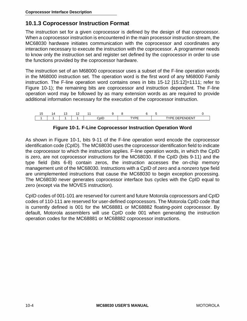
Coprocessor Interface Description
10-4
MC68030 USER’S MANUAL
MOTOROLA
10.1.3 Coprocessor Instruction Format
The instruction set for a given coprocessor is defined by the design of that coprocessor.When a coprocessor instruction is encountered in the main processor instruction stream, theMC68030 hardware initiates communication with the coprocessor and coordinates anyinteraction necessary to execute the instruction with the coprocessor. A programmer needsto know only the instruction set and register set defined by the coprocessor in order to usethe functions provided by the coprocessor hardware.
The instruction set of an M68000 coprocessor uses a subset of the F-line operation wordsin the M68000 instruction set. The operation word is the first word of any M68000 Familyinstruction. The F-line operation word contains ones in bits 15-12 [15:12]=1111; refer toFigure 10-1); the remaining bits are coprocessor and instruction dependent. The F-lineoperation word may be followed by as many extension words as are required to provideadditional information necessary for the execution of the coprocessor instruction.
Figure 10-1. F-Line Coprocessor Instruction Operation Word
As shown in Figure 10-1, bits 9-11 of the F-line operation word encode the coprocessoridentification code (CpID). The MC68030 uses the coprocessor identification field to indicatethe coprocessor to which the instruction applies. F-line operation words, in which the CpIDis zero, are not coprocessor instructions for the MC68030. If the CpID (bits 9-11) and thetype field (bits 6-8) contain zeros, the instruction accesses the on-chip memorymanagement unit of the MC68030. Instructions with a CpID of zero and a nonzero type fieldare unimplemented instructions that cause the MC68030 to begin exception processing.The MC68030 never generates coprocessor interface bus cycles with the CpID equal tozero (except via the MOVES instruction).
CpID codes of 001-101 are reserved for current and future Motorola coprocessors and CpIDcodes of 110-111 are reserved for user-defined coprocessors. The Motorola CpID code thatis currently defined is 001 for the MC68881 or MC68882 floating-point coprocessor. Bydefault, Motorola assemblers will use CpID code 001 when generating the instructionoperation codes for the MC68881 or MC68882 coprocessor instructions.
15 14 13 12 11 9 8 6 5 01 1 1 1 CpID TYPE TYPE DEPENDENT
Coprocessor Interface Description
MOTOROLA
MC68030 USER’S MANUAL
10-5
The encoding of bits 0-8 of the coprocessor instruction operation word is dependent on theparticular instruction being implemented (see
10.2 Coprocessor Instruction Types
).
10.1.4 Coprocessor System Interface
The communication protocol between the main processor and coprocessor necessary toexecute a coprocessor instruction uses a group of interface registers, called coprocessorinterface registers, resident within the coprocessor. By accessing one of these interfaceregisters, the MC68030 hardware initiates coprocessor instructions. The coprocessor usesa set of response primitive codes and format codes defined for the M68000 coprocessorinterface to communicate status and service requests to the main processor through theseregisters. The coprocessor interface registers (CIRs) are also used to pass operandsbetween the main processor and the coprocessor. The CIR set, response primitives, andformat codes are discussed in
10.3 Coprocessor Interface Register Set
and
10.4Coprocessor Response Primitives
.
10.1.4.1 COPROCESSOR CLASSIFICATION.
M68000 coprocessors can be classifiedinto two categories depending on their bus interface capabilities. The first category, non-DMA coprocessors, consists of coprocessors that always operate as bus slaves. Thesecond category, DMA coprocessors, consists of coprocessors that operate as bus slaveswhile communicating with the main processor across the coprocessor interface, but alsohave the ability to operate as bus masters, directly controlling the system bus.
If the operation of a coprocessor does not require a large portion of the available busbandwidth or has special requirements not directly satisfied by the main processor, thatcoprocessor can be efficiently implemented as a non-DMA coprocessor. Since non-DMAcoprocessors always operate as bus slaves, all external bus-related functions that thecoprocessor requires are performed by the main processor. The main processor transfersoperands from the coprocessor by reading the operand from the appropriate CIR and thenwriting the operand to a specified effective address with the appropriate address spacespecified on the function code lines. Likewise, the main processor transfers operands to thecoprocessor by reading the operand from a specified effective address (and address space)and then writing that operand to the appropriate CIR using the coprocessor interface. Thebus interface circuitry of a coprocessor operating as a bus slave is not as complex as thatof a device operating as a bus master.

Coprocessor Interface Description
10-6
MC68030 USER’S MANUAL
MOTOROLA
To improve the efficiency of operand transfers between memory and the coprocessor, acoprocessor that requires a relatively high amount of bus bandwidth or has special busrequirements can be implemented as a DMA coprocessor. DMA coprocessors can operateas bus masters. The coprocessor provides all control, address, and data signals necessaryto request and obtain the bus and then performs DMA transfers using the bus. DMAcoprocessors, however, must still act as bus slaves when they require information orservices of the main processor using the M68000 coprocessor interface protocol.
10.1.4.2 PROCESSOR-COPROCESSOR INTERFACE.
Figure 10-2 is a block diagram ofthe signals involved in an asynchronous non-DMA M68000 coprocessor interface. Thesynchronous interface is similar. Since the CpID on signals A13-A15 of the address bus isused with other address signals to select the coprocessor, the system designer can useseveral coprocessors of the same type and assign a unique CpID to each one.
The MC68030 accesses the registers in the CIR set using standard asynchronous orsynchronous bus cycles. Thus, the bus interface implemented by a coprocessor for itsinterface register set must satisfy the MC68030 address, data, and control signal timing. TheMC68030 timing information for read and write cycles is illustrated in Figures 13-5-13-8 onfoldout pages in the back of this manual. The MC68030 never requests a burst operation
Figure 10-2. Asynchronous Non-DMA M68000 CoprocessorInterface Signal Usage
FC2-FC0
A19-A13
COPROCESSORDECODE
LOGIC
CS COPROCESSOR
ASYNCHRONOUSBUS
INTERFACELOGIC
AS
DS
R/W
A4-A1
D31-D0
DSACK1/DSACK0
MAIN CONTROLLERMC68EC030
FC2-FC0 = 111 CPU SPACE CYCLEA19-A16 = 0010 COPROCESSOR ACCESS IN CPU SPACEA15-A13 = xxx COPROCESSOR IDENTIFICATIONA4-A1 = rrrr COPROCESSOR INTERFACE REGISTER SELECTOR
Chip select logic may be integrated into the coprocessor.Address lines not specified above are "0" during coprocessor access.
➧ ➧➧➧
*
*

Coprocessor Interface Description
MOTOROLA
MC68030 USER’S MANUAL
10-7
during a coprocessor (CPU space) bus cycle, nor does it internally cache data read orwritten during coprocessor (CPU space) bus cycles. The MC68030 bus operation isdescribed in detail in
Section 7 Bus Operation
.
During coprocessor instruction execution, the MC68030 executes CPU space bus cycles toaccess the CIR set. The MC68030 drives the three function code outputs high(FC2:FC0=111) identifying a CPU space bus cycle. The CIR set is mapped into CPU spacein the same manner that a peripheral interface register set is generally mapped into dataspace. The information encoded on the function code lines and address bus of the MC68030during a coprocessor access is used to generate the chip select signal for the coprocessorbeing accessed. Other address lines select a register within the interface set. Theinformation encoded on the function code and address lines of the MC68030 during acoprocessor access is illustrated in Figure 10-3.
Address signals A16-A19 specify the CPU space cycle type for a CPU space bus cycle. Thetypes of CPU space cycles currently defined for the MC68030 are interrupt acknowledge,breakpoint acknowledge, and coprocessor access cycles. CPU space type $2(A19:A16=0010) specifies a coprocessor access cycle.
Signals A13-A15 of the MC68030 address bus specify the coprocessor identification codeCpID for the coprocessor being accessed. This code is transferred from bits 9-11 of thecoprocessor instruction operation word (refer to Figure 10-1) to the address bus during eachcoprocessor access. Thus, decoding the MC68030 function code signals and bits A13-A19of the address bus provides a unique chip select signal for a given coprocessor. The functioncode signals and A16-A19 indicate a coprocessor access; A13-A15 indicate which of thepossible seven coprocessors (001-111) is being accessed. Bits A20-A31 and A5-A12 of theMC68030 address bus are always zero during a coprocessor access.
The MC68010 can emulate coprocessor access cycles in CPU space using the MOVESinstruction.
10.1.4.3 COPROCESSOR INTERFACE REGISTER SELECTION.
Figure 10-4 shows thatthe value on the MC68030 address bus during a coprocessor access addresses a uniqueregion of the main processor's CPU address space. Signals A0–A4 of the MC68030 addressbus select the CIR being accessed. The register map for the M68000 coprocessor interfaceis shown in Figure 10-5. The individual registers are described in detail in
10.3 CoprocessorInterface Register Set
.
Figure 10-3. MC68030 CPU Space Address Encodings
1 1 1 0 0 0 0 0 0 0 0 0 0 0 0 0 01 CpID 0 0 0 0 0 0 0 CIR0 0
FUNCTIONCODE
2 0 31 19 15 12 4 0
ADDRESS BUS
CPU SPACE TYPE FIELD
1320 16 5

Coprocessor Interface Description
10-8
MC68030 USER’S MANUAL
MOTOROLA
Figure 10-4. Coprocessor Address Map in MC68030 CPU Space
INTERFACE REGISTER SET
RESERVED
INTERFACE REGISTER SET
RESERVED
INTERFACE REGISTER SET
RESERVED
CPU SPACE ADDRESS
2000
2001F
22000
2201F
24000
2E000
2E01F
ADDRESS SPACE FORCOPROCESSOR WITHCpID = 0
ADDRESS SPACE FORCOPROCESSOR WITHCpID = 1
ADDRESS SPACE FORCOPROCESSOR WITHCpID = 7

Coprocessor Interface Description
MOTOROLA
MC68030 USER’S MANUAL
10-9
Figure 10-5. Coprocessor Interface Register Set Map
10.2 COPROCESSOR INSTRUCTION TYPES
The M68000 coprocessor interface supports four categories of coprocessor instructions:general, conditional, context save, and context restore. The category name indicates thetype of operations provided by the coprocessor instructions in the category. The instructioncategory also determines the CIR accessed by the MC68030 to initiate instruction andcommunication protocols between the main processor and the coprocessor necessary forinstruction execution.
During the execution of instructions in the general or conditional categories, the coprocessoruses the set of coprocessor response primitive codes defined for the MC68000 coprocessorinterface to request services from and indicate status to the main processor. During theexecution of the instructions in the context save and context restore categories, thecoprocessor uses the set of coprocessor format codes defined for the M68000 coprocessorinterface to indicate its status to the main processor.
10.2.1 Coprocessor General Instructions
The general coprocessor instruction category contains data processing instructions andother general-purpose instructions for a given coprocessor.
31 15 0
00 RESPONSE* CONTROL*04 SAVE* RESTORE*08 OPERATION WORD COMMAND*0C (RESERVED) CONDITION*10 OPERAND*14 REGISTER SELECT (RESERVED)18 INSTRUCTION ADDRESS1C OPERAND ADDRESS
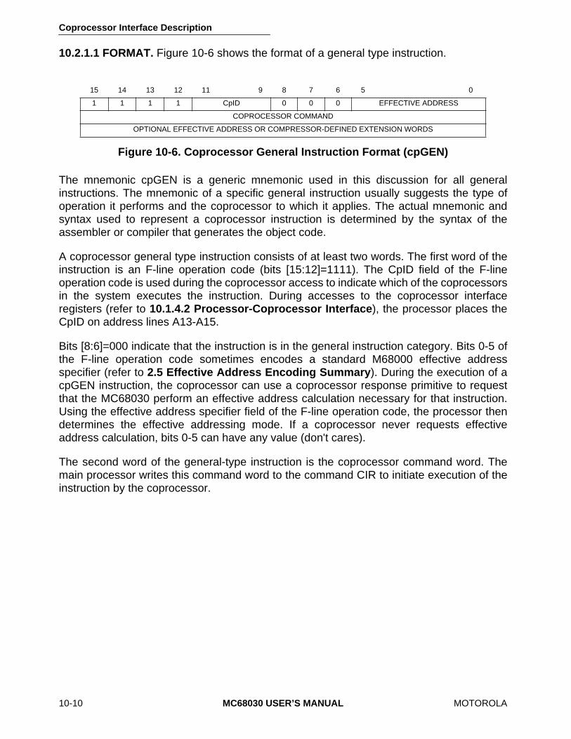
Coprocessor Interface Description
10-10
MC68030 USER’S MANUAL
MOTOROLA
10.2.1.1 FORMAT.
Figure 10-6 shows the format of a general type instruction.
Figure 10-6. Coprocessor General Instruction Format (cpGEN)
The mnemonic cpGEN is a generic mnemonic used in this discussion for all generalinstructions. The mnemonic of a specific general instruction usually suggests the type ofoperation it performs and the coprocessor to which it applies. The actual mnemonic andsyntax used to represent a coprocessor instruction is determined by the syntax of theassembler or compiler that generates the object code.
A coprocessor general type instruction consists of at least two words. The first word of theinstruction is an F-line operation code (bits [15:12]=1111). The CpID field of the F-lineoperation code is used during the coprocessor access to indicate which of the coprocessorsin the system executes the instruction. During accesses to the coprocessor interfaceregisters (refer to
10.1.4.2 Processor-Coprocessor Interface
), the processor places theCpID on address lines A13-A15.
Bits [8:6]=000 indicate that the instruction is in the general instruction category. Bits 0-5 ofthe F-line operation code sometimes encodes a standard M68000 effective addressspecifier (refer to
2.5 Effective Address Encoding Summary
). During the execution of acpGEN instruction, the coprocessor can use a coprocessor response primitive to requestthat the MC68030 perform an effective address calculation necessary for that instruction.Using the effective address specifier field of the F-line operation code, the processor thendetermines the effective addressing mode. If a coprocessor never requests effectiveaddress calculation, bits 0-5 can have any value (don't cares).
The second word of the general-type instruction is the coprocessor command word. Themain processor writes this command word to the command CIR to initiate execution of theinstruction by the coprocessor.
15 14 13 12 11 9 8 7 6 5 0
1 1 1 1 CpID 0 0 0 EFFECTIVE ADDRESS
COPROCESSOR COMMAND
OPTIONAL EFFECTIVE ADDRESS OR COMPRESSOR-DEFINED EXTENSION WORDS

Coprocessor Interface Description
MOTOROLA
MC68030 USER’S MANUAL
10-11
An instruction in the coprocessor general instruction category optionally includes a numberof extension words following the coprocessor command word. These words can provideadditional information required for the coprocessor instruction. For example, if thecoprocessor requests that the MC68030 calculate an effective address during coprocessorinstruction execution, information required for the calculation must be included in theinstruction format as effective address extension words.
10.2.1.2 PROTOCOL.
The execution of a cpGEN instruction follows the protocol shown inFigure 10-7. The main processor initiates communication with the coprocessor by writing theinstruction command word to the command CIR. The coprocessor decodes the commandword to begin processing the cpGEN instruction. Coprocessor design determines theinterpretation of the coprocessor command word; the MC68030 does not attempt to decodeit.
While the coprocessor is executing an instruction, it requests any required services from andcommunicates status to the main processor by placing coprocessor response primitivecodes in the response CIR. After writing to the command CIR, the main processor reads theresponse CIR and responds appropriately. When the coprocessor has completed theexecution of an instruction or no longer needs the services of the main processor to executethe instruction, it provides a response to release the processor. The main processor canthen execute the next instruction in the instruction stream. However, if a trace exception ispending, the MC68030 does not terminate communication with the coprocessor until thecoprocessor indicates that it has completed all processing associated with the cpGENinstruction (refer to
10.5.2.5 Trace Exceptions
).
The coprocessor interface protocol shown in Figure 10-7 allows the coprocessor to definethe operation of each general category instruction. That is, the main processor initiates theinstruction execution by writing the instruction command word to the command CIR and byreading the response CIR to determine its next action. The execution of the coprocessorinstruction is then defined by the internal operation of the coprocessor and by its use ofresponse primitives to request services from the main processor. This instruction protocolallows a wide range of operations to be implemented in the general instruction category.
10.2.2 Coprocessor Conditional Instructions
The conditional instruction category provides program control based on the operations ofthe coprocessor. The coprocessor evaluates a condition and returns a true/false indicatorto the main processor. The main processor completes the execution of the instruction basedon this true/false condition indicator.
The implementation of instructions in the conditional category promotes efficient use of boththe main processor's and the coprocessor's hardware. The condition specified for theinstruction is related to the coprocessor operation and is, therefore, evaluated by the
(UNABLE TO LOCATE ART)
Figure 10-7. Coprocessor Interface Protocol forGeneral Category Instructions
Coprocessor Interface Description
10-12
MC68030 USER’S MANUAL
MOTOROLA
coprocessor. The instruction completion following the condition evaluation is, however,directly related to the operation of the main processor. The main processor performs thechange of flow, the setting of a byte, or the TRAP operation, since its architecture explicitlyimplements these operations for its instruction set.
Coprocessor Interface Description
MOTOROLA
MC68030 USER’S MANUAL
10-13
Figure 10-8 shows the protocol for a conditional category coprocessor instruction. The mainprocessor initiates execution of an instruction in this category by writing a condition selectorto the condition CIR. The coprocessor decodes the condition selector to determine thecondition to evaluate. The coprocessor can use response primitives to request that the mainprocessor provide services required for the condition evaluation. After evaluating thecondition, the coprocessor returns a true/false indicator to the main processor by placing anull primitive (refer to
10.4.4 Null Primitive
) in the response CIR. The main processorcompletes the coprocessor instruction execution when it receives the condition indicatorfrom the coprocessor.
10.2.2.1 BRANCH ON COPROCESSOR CONDITION INSTRUCTION.
The conditionalinstruction category includes two formats of the M68000 Family branch instruction. Theseinstructions branch on conditions related to the coprocessor operation. They executesimilarly to the conditional branch instructions provided in the M68000 Family instruction set.
10.2.2.1.1 Format.
Figure 10-9 shows the format of the branch on coprocessor conditioninstruction that provides a word-length displacement. Figure 10-10. shows the format of theinstruction that includes a long-word displacement.
Figure 10-9. Branch on Coprocessor Condition Instruction (cpBcc.W)
Figure 10-10. Branch On Coprocessor Condition Instruction (cpBcc.L)
The first word of the branch on coprocessor condition instruction is the F-line operationword. Bits [15:12]=1111 and bits [11:9] contain the identification code of the coprocessorthat is to evaluate the condition. The value in bits [8:6] identifies either the word or the long-word displacement format of the branch instruction, which is specified by the cpBcc.W orcpBcc.L mnemonic, respectively.
(UNABLE TO LOCATE ART)
Figure 10-8. Coprocessor Interface Protocol for ConditionalCategory Instructions
15 14 13 12 11 9 8 7 6 5 0
1 1 1 1 CpID 0 1 0 CONDITION SELECTOR
OPTIONAL COPROCESSOR-DEFINED WORDS
DISPLACEMENT
15 14 13 12 11 9 8 7 6 5 0
1 1 1 1 CpID 0 1 1 CONDITION SELECTOR
OPTIONAL COPROCESSOR-DEFINED WORDS
DISPLACEMENT-HIGH
DISPLACEMENT-LOW

Coprocessor Interface Description
10-14
MC68030 USER’S MANUAL
MOTOROLA
Bits [0-5] of the F-line operation word contain the coprocessor condition selector field. TheMC68030 writes the entire operation word to the condition CIR to initiate execution of thebranch instruction by the coprocessor. The coprocessor uses bits [0-5] to determine whichcondition to evaluate.
If the coprocessor requires additional information to evaluate the condition, the branchinstruction format can include this information in extension words. Following the F-lineoperation word, the number of extension words is determined by the coprocessor design.The final word(s) of the cpBcc instruction format contains the displacement used by the mainprocessor to calculate the destination address when the branch is taken.
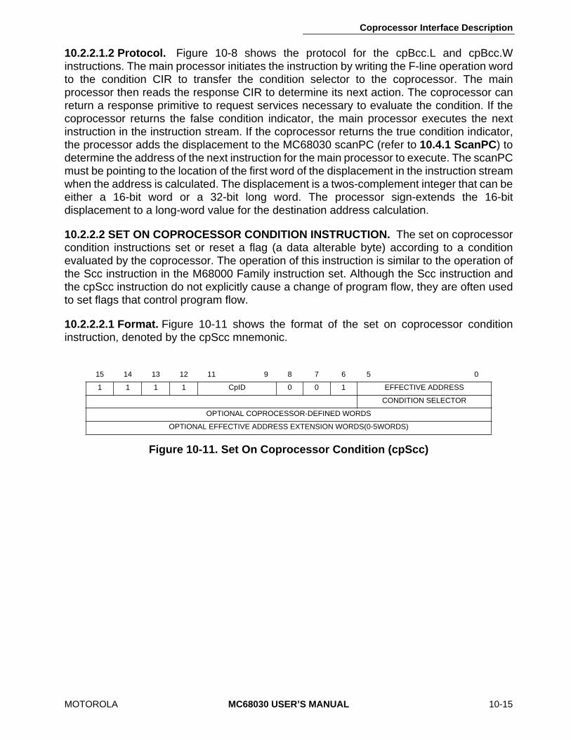
Coprocessor Interface Description
MOTOROLA
MC68030 USER’S MANUAL
10-15
10.2.2.1.2 Protocol.
Figure 10-8 shows the protocol for the cpBcc.L and cpBcc.Winstructions. The main processor initiates the instruction by writing the F-line operation wordto the condition CIR to transfer the condition selector to the coprocessor. The mainprocessor then reads the response CIR to determine its next action. The coprocessor canreturn a response primitive to request services necessary to evaluate the condition. If thecoprocessor returns the false condition indicator, the main processor executes the nextinstruction in the instruction stream. If the coprocessor returns the true condition indicator,the processor adds the displacement to the MC68030 scanPC (refer to
10.4.1 ScanPC
) todetermine the address of the next instruction for the main processor to execute. The scanPCmust be pointing to the location of the first word of the displacement in the instruction streamwhen the address is calculated. The displacement is a twos-complement integer that can beeither a 16-bit word or a 32-bit long word. The processor sign-extends the 16-bitdisplacement to a long-word value for the destination address calculation.
10.2.2.2 SET ON COPROCESSOR CONDITION INSTRUCTION.
The set on coprocessorcondition instructions set or reset a flag (a data alterable byte) according to a conditionevaluated by the coprocessor. The operation of this instruction is similar to the operation ofthe Scc instruction in the M68000 Family instruction set. Although the Scc instruction andthe cpScc instruction do not explicitly cause a change of program flow, they are often usedto set flags that control program flow.
10.2.2.2.1 Format.
Figure 10-11 shows the format of the set on coprocessor conditioninstruction, denoted by the cpScc mnemonic.
Figure 10-11. Set On Coprocessor Condition (cpScc)
15 14 13 12 11 9 8 7 6 5 0
1 1 1 1 CpID 0 0 1 EFFECTIVE ADDRESS
CONDITION SELECTOR
OPTIONAL COPROCESSOR-DEFINED WORDS
OPTIONAL EFFECTIVE ADDRESS EXTENSION WORDS(0-5WORDS)
Coprocessor Interface Description
10-16
MC68030 USER’S MANUAL
MOTOROLA
The first word of the cpScc instruction is the F-line operation word. This word contains theCpID field in bits [9-11] and 001 in bits [8:6] to identify the cpScc instruction. The lower sixbits of the F-line operation word are used to encode an M68000 Family effective addressingmode (refer to
2.5 Effective Address Encoding Summary
).
The second word of the cpScc instruction format contains the coprocessor conditionselector in bits [0-5]. Bits [6-15] of this word are reserved by Motorola and should be zero toensure compatibility with future M68000 products. This word is written to the condition CIRto initiate the cpScc instruction.
If the coprocessor requires additional information to evaluate the condition, the instructioncan include extension words to provide this information. The number of these extensionwords, which follow the word containing the coprocessor condition selector field, isdetermined by the coprocessor design.
The final portion of the cpScc instruction format contains zero to five effective addressextension words. These words contain any additional information required to calculate theeffective address specified by bits [0-5] of the F-line operation word.
10.2.2.2.2 Protocol.
Figure 10-8 shows the protocol for the cpScc instruction. TheMC68030 transfers the condition selector to the coprocessor by writing the word 22followingthe F-line operation word to the condition CIR. The main processor then reads the responseCIR to determine its next action. The coprocessor can return a response primitive to requestservices necessary to evaluate the condition. The operation of the cpScc instructiondepends on the condition evaluation indicator returned to the main processor by thecoprocessor. When the coprocessor returns the false condition indicator, the mainprocessor evaluates the effective address specified by bits [0-5] of the F-line operation wordand sets the byte at that effective address to FALSE (all bits cleared). When the coprocessorreturns the true condition indicator, the main processor sets the byte at the effective addressto TRUE (all bits set to one).
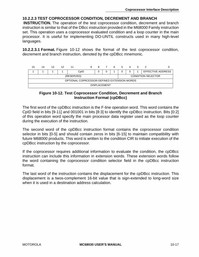
Coprocessor Interface Description
MOTOROLA
MC68030 USER’S MANUAL
10-17
10.2.2.3 TEST COPROCESSOR CONDITION, DECREMENT AND BRANCH INSTRUCTION.
The operation of the test coprocessor condition, decrement and branchinstruction is similar to that of the DBcc instruction provided in the M68000 Family instructionset. This operation uses a coprocessor evaluated condition and a loop counter in the mainprocessor. It is useful for implementing DO-UNTIL constructs used in many high-levellanguages.
10.2.2.3.1 Format.
Figure 10-12 shows the format of the test coprocessor condition,decrement and branch instruction, denoted by the cpDBcc mnemonic.
Figure 10-12. Test Coprocessor Condition, Decrement and BranchInstruction Format (cpDBcc)
The first word of the cpDBcc instruction is the F-line operation word. This word contains theCpID field in bits [9-11] and 001001 in bits [8:3] to identify the cpDBcc instruction. Bits [0:2]of this operation word specify the main processor data register used as the loop counterduring the execution of the instruction.
The second word of the cpDBcc instruction format contains the coprocessor conditionselector in bits [0-5] and should contain zeros in bits [6-15] to maintain compatibility withfuture M68000 products. This word is written to the condition CIR to initiate execution of thecpDBcc instruction by the coprocessor.
If the coprocessor requires additional information to evaluate the condition, the cpDBccinstruction can include this information in extension words. These extension words followthe word containing the coprocessor condition selector field in the cpDBcc instructionformat.
The last word of the instruction contains the displacement for the cpDBcc instruction. Thisdisplacement is a twos-complement 16-bit value that is sign-extended to long-word sizewhen it is used in a destination address calculation.
15 14 13 12 11 9 8 7 6 5 4 3 2 0
1 1 1 1 CpID 0 0 1 0 0 1 EFFECTIVE ADDRESS
(RESERVED) CONDITION SELECTOR
OPTIONAL COPRCESSOR-DEFINED EXTENSION WORDS
DISPLACEMENT

Coprocessor Interface Description
10-18
MC68030 USER’S MANUAL
MOTOROLA
10.2.2.3.2 Protocol.
Figure 10-8 shows the protocol for the cpDBcc instructions. TheMC68030 transfers the condition selector to the coprocessor by writing the word followingthe operation word to the condition CIR. The main processor then reads the response CIRto determine its next action. The coprocessor can use a response primitive to request anyservices necessary to evaluate the condition. If the coprocessor returns the true conditionindicator, the main processor executes the next instruction in the instruction stream. If thecoprocessor returns the false condition indicator, the main processor decrements the low-order word of the register specified by bits [0-2] of the F-line operation word. If this registercontains minus one (—1) after being decremented, the main processor executes the nextinstruction in the instruction stream. If the register does not contain minus one (—1) afterbeing decremented, the main processor branches to the destination address to continueinstruction execution.
The MC68030 adds the displacement to the scanPC (refer to
10.4.1 ScanPC
) to determinethe address of the next instruction. The scanPC must point to the 16-bit displacement in theinstruction stream when the destination address is calculated.
10.2.2.4 TRAP ON COPROCESSOR CONDITION.
The trap on coprocessor conditioninstruction allows the programmer to initiate exception processing based on conditionsrelated to the coprocessor operation.
10.2.2.4.1 Format.
Figure 10-13 shows the format of the trap on coprocessor conditioninstruction, denoted by the cpTRAPcc mnemonic.
Figure 10-13. Trap On Coprocessor Condition (cpTRAPcc)
15 14 13 12 11 9 8 7 6 5 4 3 2 0
1 1 1 1 CpID 0 0 1 1 1 1 OPMODE
(RESERVED) CONDITION SELECTOR
OPTIONAL COPRCESSOR-DEFINED EXTENSION WORDS
OPTIONAL WORD
OR LONG-WORD OPERAND

Coprocessor Interface Description
MOTOROLA
MC68030 USER’S MANUAL
10-19
The F-line operation word contains the CpID field in bits [9-11] and 001111 in bits [8:3] toidentify the cpTRAPcc instruction. Bits [0-2] of the cpTRAPcc F-line operation word specifythe number of optional operand words in the instruction format. The instruction format caninclude zero, one, or two operand words.
The second word of the cpTRAPcc instruction format contains the coprocessor conditionselector in bits [0-5] and should contain zeros in bits [6-15] to maintain compatibility withfuture M68000 products. This word is written to the condition CIR of the coprocessor toinitiate execution of the cpTRAPcc instruction by the coprocessor.
If the coprocessor requires additional information to evaluate a condition, the instruction caninclude this information in extension words. These extension words follow the wordcontaining the coprocessor condition selector field in the cpTRAPcc instruction format.
The operand words of the cpTRAPcc F-line operation word follow the coprocessor-definedextension words. These operand words are not explicitly used by the MC68030, but can beused to contain information referenced by the cpTRAPcc exception handling routines. Thevalid encodings for bits [0-2] of the F-line operation word and the corresponding numbers ofoperand words are listed in Table 10-1. Other encodings of these bits are invalid for thecpTRAPcc instruction.
10.2.2.4.2 Protocol. Figure 10-8 shows the protocol for the cpTRAPcc instructions. TheMC68030 transfers the condition selector to the coprocessor by writing the word followingthe operation word to the condition CIR. The main processor then reads the response CIRto determine its next action. The coprocessor can, using a response primitive, request anyservices necessary to evaluate the condition. If the coprocessor returns the true conditionindicator, the main processor initiates exception processing for the cpTRAPcc exception(refer to 10.5.2.4 cpTRAPcc Instruction Traps). If the coprocessor returns the falsecondition indicator, the main processor executes the next instruction in the instructionstream.
Table 10-1. cpTRAPcc Opmode
OpmodeOptional Words in
instructional Format010 One011 Two100 Zero
Coprocessor Interface Description
10-20 MC68030 USER’S MANUAL MOTOROLA
10.2.3 Coprocessor Save and Restore InstructionsThe coprocessor context save and context restore instruction categories in the M68000coprocessor interface support multitasking programming environments. In a multitaskingenvironment, the context of a coprocessor may need to be changed asynchronously withrespect to the operation of that coprocessor. That is, the coprocessor may be interrupted atany point in the execution of an instruction in the general or conditional category to begincontext change operations.
In contrast to the general and conditional instruction categories, the context save andcontext restore instruction categories do not use the coprocessor response primitives. A setof format codes defined by the M68000 coprocessor interface communicates statusinformation to the main processor during the execution of these instructions. Thesecoprocessor format codes are discussed in detail in 10.2.3.2 Coprocessor Format Words.
10.2.3.1 COPROCESSOR INTERNAL STATE FRAMES. The context save (cpSAVE) andcontext restore (cpRESTORE) instructions transfer an internal coprocessor state framebetween memory and a coprocessor. This internal coprocessor state frame represents thestate of coprocessor operations. Using the cpSAVE and cpRESTORE instructions, it ispossible to interrupt coprocessor operation, save the context associated with the currentoperation, and initiate coprocessor operations with a new context.
A cpSAVE instruction stores a coprocessor's internal state frame as a sequence of long-word entries in memory. Figure 10-14 shows the format of a coprocessor state frame. Duringexecution of the cpSAVE instruction, the MC68030 calculates the state frame effectiveaddress from information in the operation word of the instruction and stores a format wordat this effective address. The processor writes the long words that form the coprocessorstate frame to descending memory addresses, beginning with the address specified by thesum of the effective address and the format word-length field multiplied by four. Duringexecution of the cpRESTORE instruction, the MC68030 reads the format word and longwords in the state frame from ascending addresses, beginning with the effective addressspecified in the instruction operation word.

Coprocessor Interface Description
MOTOROLA MC68030 USER’S MANUAL 10-21
The processor stores the coprocessor format word at the lowest address of the state framein memory, and this word is the first word transferred for both the cpSAVE and thecpRESTORE instructions. The word following the format word does not contain informationrelevant to the coprocessor state frame, but serves to keep the information in the state framea multiple of four bytes in size. The number of entries following the format word (at higheraddresses) is determined.
The information in a coprocessor state frame describes a context of operation for thatcoprocessor. This description of a coprocessor context includes the program invisible stateinformation and, optionally, the program visible state information. The program invisiblestate information consists of any internal registers or status information that cannot beaccessed by the program but is necessary for the coprocessor to continue its operation atthe point of suspension. Program visible state information includes the contents of allregisters that appear in the coprocessor programming model and that can be directlyaccessed using the coprocessor instruction set. The information saved by the cpSAVEinstruction must include the program invisible state information. If cpGEN instructions areprovided to save the program visible state of the coprocessor, the cpSAVE andcpRESTORE instructions should only transfer the program invisible state information tominimize interrupt latency during a save or restore operation.
Figure 10-14. Coprocessor State Frame Format in Memory
SAVEORDER
RESTOREORDER
0
n
n-1
n-2
0
1
2
3
FORMAT LENGTH (UNUSED, RESERVED)
31 23 15 0
COPROCESSOR-DEPENDENT INFORMATION
n1

Coprocessor Interface Description
10-22 MC68030 USER’S MANUAL MOTOROLA
10.2.3.2 COPROCESSOR FORMAT WORDS. The coprocessor communicates statusinformation to the main processor during the execution of cpSAVE and cpRESTOREinstructions using coprocessor format words. The format words defined for the M68000coprocessor interface are listed in Table 10-2.
The upper byte of the coprocessor format word contains the code used to communicatecoprocessor status information to the main processor. The MC68030 recognizes four typesof format words: empty/reset, not ready, invalid format, and valid format. The MC68030interprets the reserved format codes ($03-$0F) as invalid format words. The lower byte ofthe coprocessor format word specifies the size in bytes (which must be a multiple of four) ofthe coprocessor state frame. This value is only relevant when the code byte contains thevalid format code (refer to 10.2.3.2.4 Valid Format Word).
10.2.3.2.1 Empty/Reset Format Word. the Coprocessor Returns the Empty/Reset FormatCode During a Cpsave Instruction to Indicate That the Coprocessor Contains No User-Specific InformaTion. That Is, No Coprocessor Instructions Have Been Executed SinceEither a Previous CpreStore of An Empty/Reset Format Code or the Previous HardwareReset. If the Main Processor Reads the Empty/Reset Format Word from the Save Cir Duringthe Initiation of a Cpsave InstrucTion, It Stores the Format Word At the Effective AddressSpecified in the Cpsave Instruction and Executes the Next Instruction.
When the main processor reads the empty/reset format word from memory during theexecution of the cpRESTORE instruction, it writes the format word to the restore CIR. Themain processor then reads the restore CIR and, if the coprocessor returns the empty/resetformat word, executes the next instruction. The main processor can initialize thecoprocessor by writing the empty/reset format code to the restore CIR. When thecoprocessor receives the empty/reset format code, it terminates any current operations andwaits for the main processor to initiate the next coprocessor instruction. In particular, afterthe cpRESTORE of the empty/reset format word, the execution of a cpSAVE should causethe empty/reset format word to be returned when a cpSAVE instruction is executed beforeany other coprocessor instructions. Thus, an empty/reset state frame consists only of theformat word and the following reserved word in memory (refer to Figure 10-14).
Table 10-2. Coprocessor Format Word Encodings
Format Code Length Meaning00 xx Empty/Reset01 xx Not Ready, Come Again02 xx Invalid Format
03-0F xx Undefined, Reserved10-FF Length Valid Format, Coprocessor Defined
Coprocessor Interface Description
MOTOROLA MC68030 USER’S MANUAL 10-23
10.2.3.2.2 Not Ready Format Word. When the main processor initiates a cpSAVEinstruction by reading the save CIR the coprocessor can delay the save operation byreturning a not ready format word. The main processor then services any pending interruptsand reads the save CIR again. The not ready format word delays the save operation untilthe coprocessor is ready to save its internal state. The cpSAVE instruction can suspendexecution of a general or conditional coprocessor instruction; the coprocessor can resumeexecution of the suspended instruction when the appropriate state is restored with acpRESTORE. If no further main processor services are required to complete coprocessorinstruction execution, it may be more efficient to complete the instruction and thus reducethe size of the saved state. The coprocessor designer should consider the efficiency ofcompleting the instruction or of suspending and later resuming the instruction when the mainprocessor executes a cpSAVE instruction.
When the main processor initiates a cpRESTORE instruction by writing a format word to therestore CIR, the coprocessor should usually terminate any current operations and restorethe state frame supplied by the main processor. Thus, the not ready format word shouldusually not be returned by the coprocessor during the execution of a cpRESTOREinstruction. If the coprocessor must delay the cpRESTORE operation for any reason, it canreturn the not ready format word when the main processor reads the restore CIR. If the mainprocessor reads the not ready format word from the restore CIR during the cpRESTOREinstruction, it reads the restore CIR again without servicing any pending interrupts.
10.2.3.2.3 Invalid Format Word. When the format word placed in the restore CIR to initiatea cpRESTORE instruction does not describe a valid coprocessor state frame, thecoprocessor returns the invalid format word in the restore CIR. When the main processorreads this format word during the cpRESTORE instruction, it writes the abort mask to thecontrol CIR and initiates format error exception processing. The two least significant bits ofthe abort mask are 01; the fourteen most significant bits are undefined.
Coprocessor Interface Description
10-24 MC68030 USER’S MANUAL MOTOROLA
A coprocessor should usually not place an invalid format word in the save CIR when themain processor initiates a cpSAVE instruction. A coprocessor, however, may not be able tosupport the initiation of a cpSAVE instruction while it is executing a previously initiatedcpSAVE or cpRESTORE instruction. In this situation, the coprocessor can return the invalidformat word when the main processor reads the save CIR to initiate the cpSAVE instructionwhile either another cpSAVE or cpRESTORE instruction is executing. If the main processorreads an invalid format word from the save CIR, it writes the abort mask to the control CIRand initiates format error exception processing (refer to 10.5.1.5 Format Errors).
10.2.3.2.4 Valid Format Word. When the main processor reads a valid format word fromthe save CIR during the cpSAVE instruction, it uses the length field to determine the size ofthe coprocessor state frame to save. The length field in the lower eight bits of a format wordis relevant only in a valid format word. During the cpRESTORE instruction, the mainprocessor uses the length field in the format word read from the effective address in theinstruction to determine the size of the coprocessor state frame to restore.
The length field of a valid format word, representing the size of the coprocessor state frame,must contain a multiple of four. If the main processor detects a value that is not a multiple offour in a length field during the execution of a cpSAVE or cpRESTORE instruction, the mainprocessor writes the abort mask (refer to 10.2.3.2.3 Invalid Format Word) to the controlCIR and initiates format error exception processing.
10.2.3.3 COPROCESSOR CONTEXT SAVE INSTRUCTION. The M68000 coprocessorcontext save instruction category consists of one instruction. The coprocessor context saveinstruction, denoted by the cpSAVE mnemonic, saves the context of a coprocessordynamically without relation to the execution of coprocessor instructions in the general orconditional instruction categories. During the execution of a cpSAVE instruction, thecoprocessor communicates status information to the main processor by using thecoprocessor format codes.
10.2.3.3.1 Format. Figure 10-15 shows the format of the cpSAVE instruction. The first wordof the instruction is the F-line operation word, which contains the coprocessor identificationcode in bits [9-11] and an M68000 effective address code in bits [0-5]. The effective addressencoded in the cpSAVE instruction is the address at which the state frame associated withthe current context of the coprocessor is saved in memory.

Coprocessor Interface Description
MOTOROLA MC68030 USER’S MANUAL 10-25
Figure 10-15. Coprocessor Context Save Instruction Format (cpSAVE)
The control alterable and predecrement addressing modes are valid for the cpSAVEinstruction. Other addressing modes cause the MC68030 to initiate F-line emulatorexception processing as described in 10.5.2.2 F-Line Emulator Exceptions.
The instruction can include as many as five effective address extension words following thecpSAVE instruction operation word. These words contain any additional informationrequired to calculate the effective address specified by bits [0-5] of the operation word.
10.2.3.3.2 Protocol. Figure 10-16 shows the protocol for the coprocessor context saveinstruction. The main processor initiates execution of the cpSAVE instruction by reading thesave CIR. Thus, the cpSAVE instruction is the only coprocessor instruction that begins byreading from a CIR. (All other coprocessor instructions write to a CIR to initiate execution ofthe instruction by the coprocessor.) The coprocessor communicates status informationassociated with the context save operation to the main processor by placing coprocessorformat codes in the save CIR.
If the coprocessor is not ready to suspend its current operation when the main processorreads the save CIR, it returns a “not ready'“ format code. The main processor services anypending interrupts and then reads the save CIR again. After placing the not ready formatcode in the save CIR, the coprocessor should either suspend or complete the instruction itis currently executing.
15 14 13 12 11 9 8 7 6 5 0
1 1 1 1 CpID 1 0 0 EFFECTIVE ADDRESS
EFFECTIVE ADDRESS EXTENSION WORDS (0-5 WORDS)
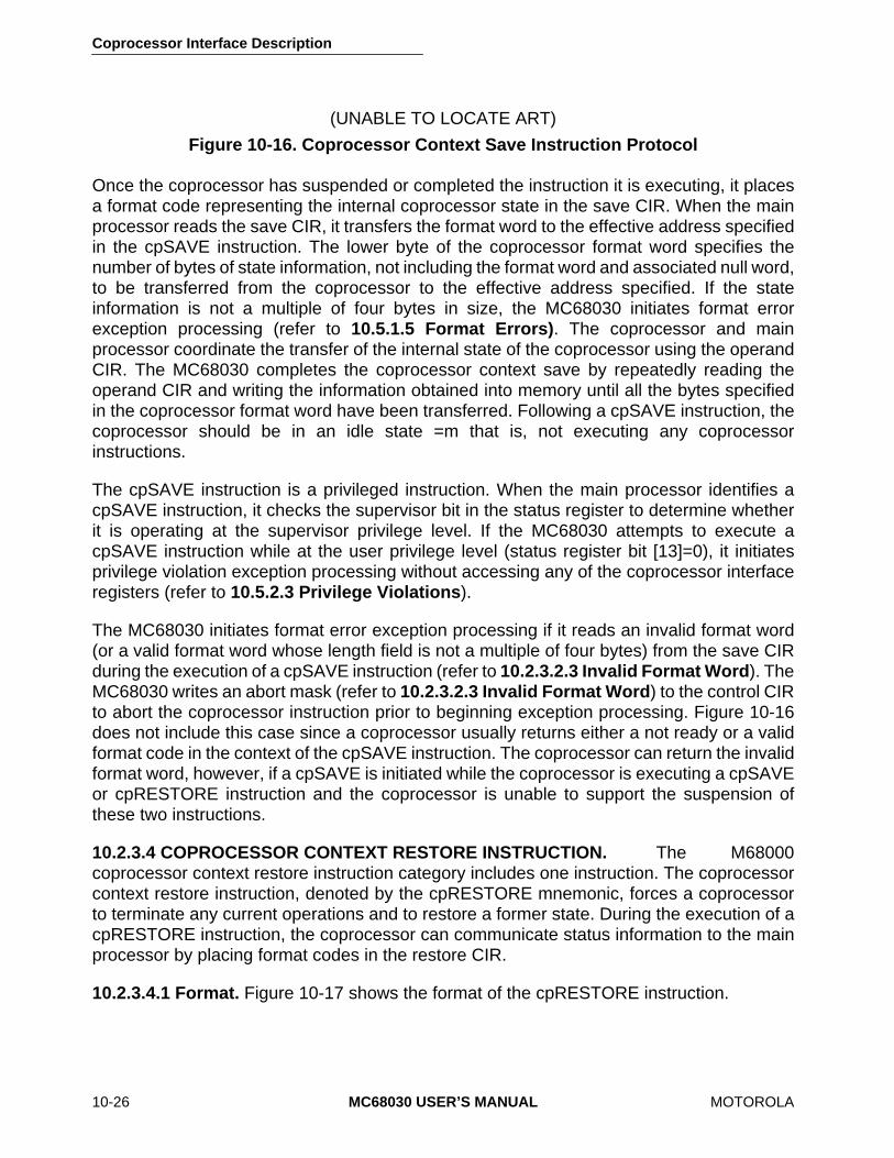
Coprocessor Interface Description
10-26 MC68030 USER’S MANUAL MOTOROLA
Once the coprocessor has suspended or completed the instruction it is executing, it placesa format code representing the internal coprocessor state in the save CIR. When the mainprocessor reads the save CIR, it transfers the format word to the effective address specifiedin the cpSAVE instruction. The lower byte of the coprocessor format word specifies thenumber of bytes of state information, not including the format word and associated null word,to be transferred from the coprocessor to the effective address specified. If the stateinformation is not a multiple of four bytes in size, the MC68030 initiates format errorexception processing (refer to 10.5.1.5 Format Errors). The coprocessor and mainprocessor coordinate the transfer of the internal state of the coprocessor using the operandCIR. The MC68030 completes the coprocessor context save by repeatedly reading theoperand CIR and writing the information obtained into memory until all the bytes specifiedin the coprocessor format word have been transferred. Following a cpSAVE instruction, thecoprocessor should be in an idle state =m that is, not executing any coprocessorinstructions.
The cpSAVE instruction is a privileged instruction. When the main processor identifies acpSAVE instruction, it checks the supervisor bit in the status register to determine whetherit is operating at the supervisor privilege level. If the MC68030 attempts to execute acpSAVE instruction while at the user privilege level (status register bit [13]=0), it initiatesprivilege violation exception processing without accessing any of the coprocessor interfaceregisters (refer to 10.5.2.3 Privilege Violations).
The MC68030 initiates format error exception processing if it reads an invalid format word(or a valid format word whose length field is not a multiple of four bytes) from the save CIRduring the execution of a cpSAVE instruction (refer to 10.2.3.2.3 Invalid Format Word). TheMC68030 writes an abort mask (refer to 10.2.3.2.3 Invalid Format Word) to the control CIRto abort the coprocessor instruction prior to beginning exception processing. Figure 10-16does not include this case since a coprocessor usually returns either a not ready or a validformat code in the context of the cpSAVE instruction. The coprocessor can return the invalidformat word, however, if a cpSAVE is initiated while the coprocessor is executing a cpSAVEor cpRESTORE instruction and the coprocessor is unable to support the suspension ofthese two instructions.
10.2.3.4 COPROCESSOR CONTEXT RESTORE INSTRUCTION. The M68000coprocessor context restore instruction category includes one instruction. The coprocessorcontext restore instruction, denoted by the cpRESTORE mnemonic, forces a coprocessorto terminate any current operations and to restore a former state. During the execution of acpRESTORE instruction, the coprocessor can communicate status information to the mainprocessor by placing format codes in the restore CIR.
10.2.3.4.1 Format. Figure 10-17 shows the format of the cpRESTORE instruction.
(UNABLE TO LOCATE ART)
Figure 10-16. Coprocessor Context Save Instruction Protocol
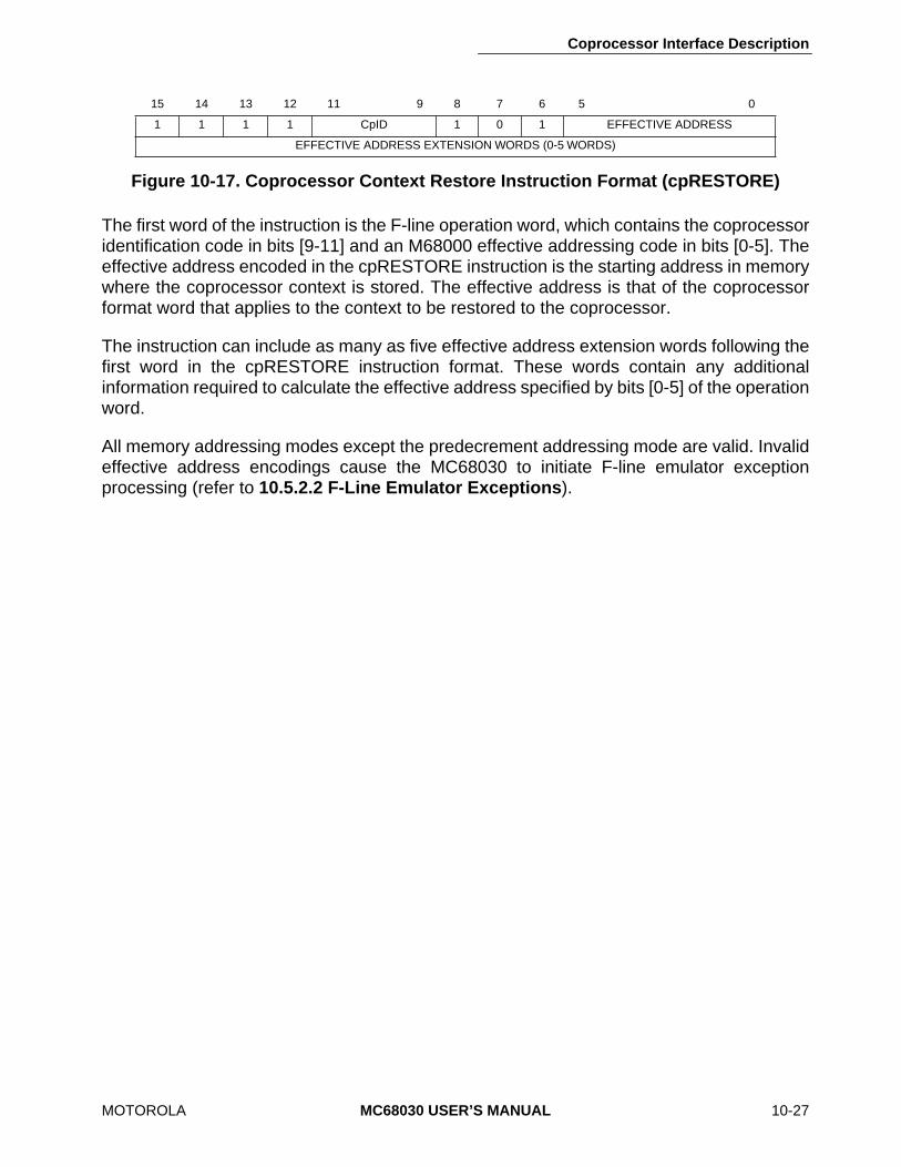
Coprocessor Interface Description
MOTOROLA MC68030 USER’S MANUAL 10-27
Figure 10-17. Coprocessor Context Restore Instruction Format (cpRESTORE)
The first word of the instruction is the F-line operation word, which contains the coprocessoridentification code in bits [9-11] and an M68000 effective addressing code in bits [0-5]. Theeffective address encoded in the cpRESTORE instruction is the starting address in memorywhere the coprocessor context is stored. The effective address is that of the coprocessorformat word that applies to the context to be restored to the coprocessor.
The instruction can include as many as five effective address extension words following thefirst word in the cpRESTORE instruction format. These words contain any additionalinformation required to calculate the effective address specified by bits [0-5] of the operationword.
All memory addressing modes except the predecrement addressing mode are valid. Invalideffective address encodings cause the MC68030 to initiate F-line emulator exceptionprocessing (refer to 10.5.2.2 F-Line Emulator Exceptions).
15 14 13 12 11 9 8 7 6 5 0
1 1 1 1 CpID 1 0 1 EFFECTIVE ADDRESS
EFFECTIVE ADDRESS EXTENSION WORDS (0-5 WORDS)

Coprocessor Interface Description
10-28 MC68030 USER’S MANUAL MOTOROLA
10.2.3.4.2 Protocol. Figure 10-18 shows the protocol for the coprocessor context restoreinstruction. When the main processor executes a cpRESTORE instruction, it first reads thecoprocessor format word from the effective address in the instruction. This format wordcontains a format code and a length field. During cpRESTORE operation, the mainprocessor retains a copy of the length field to determine the number of bytes to betransferred to the coprocessor during the cpRESTORE operation and writes the format wordto the restore CIR to initiate the coprocessor context restore.
When the coprocessor receives the format word in the restore CIR, it must terminate anycurrent operations and evaluate the format word. If the format word represents a validcoprocessor context as determined by the coprocessor design, the coprocessor returns theformat word to the main processor through the restore CIR and prepares to receive thenumber of bytes specified in the format word through its operand CIR.
After writing the format word to the restore CIR the main processor continues thecpRESTORE dialog by reading that same register. If the coprocessor returns a valid formatword, the main processor transfers the number of bytes specified by the format word at theeffective address to the operand CIR.
If the format word written to the restore CIR does not represent a valid coprocessor stateframe, the coprocessor places an invalid format word in the restore CIR and terminates anycurrent operations. The main processor receives the invalid format code, writes an abortmask (refer to 10.2.3.2.3 Invalid Format Word) to the control CIR, and initiates format errorexception processing (refer to 10.5.1.5 Format Errors).
The cpRESTORE instruction is a privileged instruction. When the main processor accessesa cpRESTORE instruction, it checks the supervisor bit in the status register. If the MC68030attempts to execute a cpRESTORE instruction while at the user privilege level (statusregister bit [13]=0), it initiates privilege violation exception processing without accessing anyof the coprocessor interface registers (refer to 10.5.2.3 Privilege Violations).
10.3 COPROCESSOR INTERFACE REGISTER SETThe instructions of the M68000 coprocessor interface use registers of the CIR set tocommunicate with the coprocessor. These CIRs are not directly related to the coprocessor'sprogramming model.
Figure 10-4 is a memory map of the CIR set. The registers denoted by asterisks (*) must beincluded in a coprocessor interface that implements coprocessor instructions in all fourcategories. The complete register model must be implemented if the system uses all of thecoprocessor response primitives defined for the M68000 coprocessor interface.
The following paragraphs contain detailed descriptions of the registers.
(UNABLE TO LOCATE ART)
Figure 10-18. Coprocessor Context Restore Instruction Protocol
Coprocessor Interface Description
MOTOROLA MC68030 USER’S MANUAL 10-29
10.3.1 Response CIRThe coprocessor uses the 16-bit response CIR to communicate all service requests(coprocessor response primitives) to the main processor. The main processor reads theresponse CIR to receive the coprocessor response primitives during the execution ofinstructions in the general and conditional instruction categories. The offset from the baseaddress of the CIR set for the response CIR is $00. Refer to 10.4 Coprocessor ResponsePrimitives.

Coprocessor Interface Description
10-30 MC68030 USER’S MANUAL MOTOROLA
10.3.2 Control CIRThe main processor writes to the 2-bit control CIR to acknowledge coprocessor-requestedexception processing or to abort the execution of a coprocessor instruction. The offset fromthe base address of the CIR set for the control CIR is $02. The control CIR occupies the twoleast significant bits of the word at that offset. The 14 most significant bits of the word areundefined. Figure 10-19 shows the format of this register.
Figure 10-19. Control CIR Format
When the MC68030 receives one of the three take exception coprocessor responseprimitives, it acknowledges the primitive by writing the exception acknowledge mask (102)to the control CIR, which sets the exception acknowledge (XA) bit. The MC68030 writes theabort mask (012), which sets the abort (AB) bit, to the control CIR to abort any coprocessorinstruction in progress. (The most significant 14 bits of both masks are undefined.) TheMC68030 aborts a coprocessor instruction when it detects one of the following exceptionconditions:
• An F-line emulator exception condition after reading a response primitive
• A privilege violation exception as it performs a supervisor check in response to a su-pervisor check primitive
• A format error exception when it receives an invalid format word or a valid format word that contains an invalid length
10.3.3 Save CIRThe coprocessor uses the 16-bit save CIR to communicate status and state frame formatinformation to the main processor while executing a cpSAVE instruction. The mainprocessor reads the save CIR to initiate execution of the cpSAVE instruction by thecoprocessor. The offset from the base address of the CIR set for the save CIR is $04. Referto 10.2.3.2 Coprocessor Format Words.
15 2 1 0
(UNDEFINED, RESERVED) XA AB

Coprocessor Interface Description
MOTOROLA MC68030 USER’S MANUAL 10-31
10.3.4 Restore CIRThe main processor initiates the cpRESTORE instruction by writing a coprocessor formatword to the 16-bit restore register. During the execution of the cpRESTORE instruction, thecoprocessor communicates status and state frame format information to the main processorthrough the restore CIR. The offset from the base address of the CIR set for the restore CIRis $06. Refer to 10.2.3.2 Coprocessor Format Words.
10.3.5 Operation Word CIRThe main processor writes the F-line operation word of the instruction in progress to the 16-bit operation word CIR in response to a transfer operation word coprocessor responseprimitive (refer to 10.4.6 Transfer Operation Word Primitive). The offset from the baseaddress of the CIR set for the operation word CIR is $08.
10.3.6 Command CIRThe main processor initiates a general category instruction by writing the instructioncommand word, which follows the instruction F-line operation word in the instruction stream,to the 16-bit command CIR. The offset from the base address of the CIR set for thecommand CIR is $0A.
10.3.7 Condition CIRThe main processor initiates a conditional category instruction by writing the conditionselector to the 16-bit condition CIR. The offset from the base address of the CIR set for thecondition CIR is $0E. Figure 10-20 shows the format of the condition CIR.
Figure 10-20. Condition CIR Format
15 6 5 0
(UNDEFINED, RESERVED) CONDITION SELECTOR
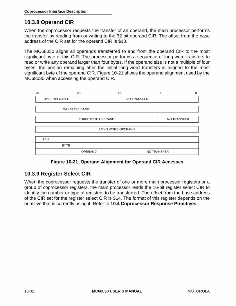
Coprocessor Interface Description
10-32 MC68030 USER’S MANUAL MOTOROLA
10.3.8 Operand CIRWhen the coprocessor requests the transfer of an operand, the main processor performsthe transfer by reading from or writing to the 32-bit operand CIR. The offset from the baseaddress of the CIR set for the operand CIR is $10.
The MC68030 aligns all operands transferred to and from the operand CIR to the mostsignificant byte of this CIR. The processor performs a sequence of long-word transfers toread or write any operand larger than four bytes. If the operand size is not a multiple of fourbytes, the portion remaining after the initial long-word transfers is aligned to the mostsignificant byte of the operand CIR. Figure 10-21 shows the operand alignment used by theMC68030 when accessing the operand CIR.
Figure 10-21. Operand Alignment for Operand CIR Accesses
10.3.9 Register Select CIRWhen the coprocessor requests the transfer of one or more main processor registers or agroup of coprocessor registers, the main processor reads the 16-bit register select CIR toidentify the number or type of registers to be transferred. The offset from the base addressof the CIR set for the register select CIR is $14. The format of this register depends on theprimitive that is currently using it. Refer to 10.4 Coprocessor Response Primitives.
31 23 15 7 0
BYTE OPERAND NO TRANSFER
WORD OPERAND
THREE BYTE OPERAND NO TRANSFER
LONG WORD OPERAND
TEN
BYTE
OPERAND NO TRANSFER
Coprocessor Interface Description
MOTOROLA MC68030 USER’S MANUAL 10-33
10.3.10 Instruction Address CIRWhen the coprocessor requests the address of the instruction it is currently executing, themain processor transfers this address to the 32-bit instruction address CIR. Any transfer ofthe scanPC is also performed through the instruction address CIR (refer to 10.4.17 TransferStatus Register and ScanPC Primitive). The offset from the base address of the CIR setfor the instruction address CIR is $18.
10.3.11 Operand Address CIRWhen a coprocessor requests an operand address transfer between the main processorand the coprocessor, the address is transferred through the 32-bit operand address CIR.The offset from the base address of the CIR set for the operand address CIR is $1C.
10.4 COPROCESSOR RESPONSE PRIMITIVESThe response primitives are primitive instructions that the coprocessor issues to the mainprocessor during the execution of a coprocessor instruction. The coprocessor usesresponse primitives to communicate status information and service requests to the mainprocessor. In response to an instruction command word written to the command CIR or acondition selector in the condition CIR, the coprocessor returns a response primitive in theresponse CIR. Within the general and conditional instruction categories, individualinstructions are distinguished by the operation of the coprocessor hardware and also byservices specified by coprocessor response primitives provided by the main processor.
Subsequent paragraphs, beginning with 10.4.2 Coprocessor Response PrimitiveGeneral Format, consist of detailed descriptions of the M68000 coprocessor responseprimitives supported by the MC68030. Any response primitive that the MC68030 does notrecognize causes it to initiate protocol violation exception processing (refer to 10.5.2.1Protocol Violations). This processing of undefined primitives supports emulation ofextensions to the M68000 coprocessor response primitive set by the protocol violationexception handler. Exception processing related to the coprocessor interface is discussedin 10.5 Exceptions.
Coprocessor Interface Description
10-34 MC68030 USER’S MANUAL MOTOROLA
10.4.1 ScanPCSeveral of the response primitives involve the scanPC, and many of them require the mainprocessor to use it while performing services requested. These paragraphs describe thescanPC and tell how it operates.
During the execution of a coprocessor instruction, the program counter in the MC68030contains the address of the F-line operation word of that instruction. A second register,called the scanPC, sequentially addresses the remaining words of the instruction.
If the main processor requires extension words to calculate an effective address ordestination address of a branch operation, it uses the scanPC to address these extensionwords in the instruction stream. Also, if a coprocessor requests the transfer of extensionwords, the scanPC addresses the extension words during the transfer. As the processorreferences each word, it increments the scanPC to point to the next word in the instructionstream. When an instruction is completed, the processor transfers the value in the scanPCto the program counter to address the operation word of the next instruction.
The value in the scanPC when the main processor reads the first response primitive afterbeginning to execute an instruction depends on the instruction being executed. For a cpGENinstruction, the scanPC points to the word following the coprocessor command word. Forthe cpBcc instructions, the scanPC points to the word following the instruction F-lineoperation word. For the cpScc, cpTRAPcc, and cpDBcc instructions, the scanPC points tothe word following the coprocessor condition specifier word.
If a coprocessor implementation uses optional instruction extension words with a general orconditional instruction, the coprocessor must use these words consistently so that thescanPC is updated accordingly during the instruction execution. Specifically, during theexecution of general category instructions, when the coprocessor terminates the instructionprotocol, the MC68030 assumes that the scanPC is pointing to the operation word of thenext instruction to be executed. During the execution of conditional category instructions,when the coprocessor terminates the instruction protocol, the MC68030 assumes that thescanPC is pointing to the word following the last of any coprocessor-defined extensionwords in the instruction format.
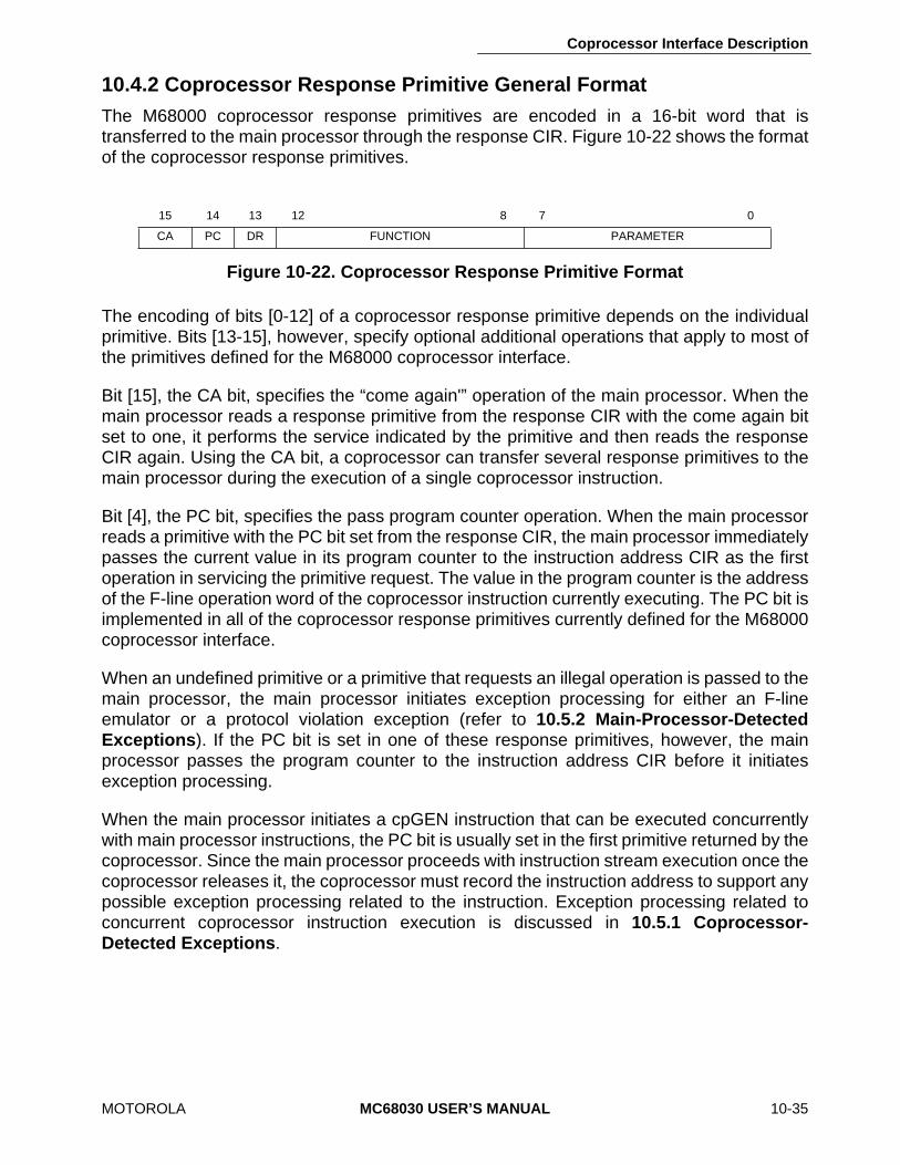
Coprocessor Interface Description
MOTOROLA MC68030 USER’S MANUAL 10-35
10.4.2 Coprocessor Response Primitive General FormatThe M68000 coprocessor response primitives are encoded in a 16-bit word that istransferred to the main processor through the response CIR. Figure 10-22 shows the formatof the coprocessor response primitives.
Figure 10-22. Coprocessor Response Primitive Format
The encoding of bits [0-12] of a coprocessor response primitive depends on the individualprimitive. Bits [13-15], however, specify optional additional operations that apply to most ofthe primitives defined for the M68000 coprocessor interface.
Bit [15], the CA bit, specifies the “come again'” operation of the main processor. When themain processor reads a response primitive from the response CIR with the come again bitset to one, it performs the service indicated by the primitive and then reads the responseCIR again. Using the CA bit, a coprocessor can transfer several response primitives to themain processor during the execution of a single coprocessor instruction.
Bit [4], the PC bit, specifies the pass program counter operation. When the main processorreads a primitive with the PC bit set from the response CIR, the main processor immediatelypasses the current value in its program counter to the instruction address CIR as the firstoperation in servicing the primitive request. The value in the program counter is the addressof the F-line operation word of the coprocessor instruction currently executing. The PC bit isimplemented in all of the coprocessor response primitives currently defined for the M68000coprocessor interface.
When an undefined primitive or a primitive that requests an illegal operation is passed to themain processor, the main processor initiates exception processing for either an F-lineemulator or a protocol violation exception (refer to 10.5.2 Main-Processor-DetectedExceptions). If the PC bit is set in one of these response primitives, however, the mainprocessor passes the program counter to the instruction address CIR before it initiatesexception processing.
When the main processor initiates a cpGEN instruction that can be executed concurrentlywith main processor instructions, the PC bit is usually set in the first primitive returned by thecoprocessor. Since the main processor proceeds with instruction stream execution once thecoprocessor releases it, the coprocessor must record the instruction address to support anypossible exception processing related to the instruction. Exception processing related toconcurrent coprocessor instruction execution is discussed in 10.5.1 Coprocessor-Detected Exceptions.
15 14 13 12 8 7 0
CA PC DR FUNCTION PARAMETER
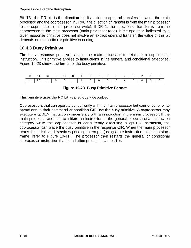
Coprocessor Interface Description
10-36 MC68030 USER’S MANUAL MOTOROLA
Bit [13], the DR bit, is the direction bit. It applies to operand transfers between the mainprocessor and the coprocessor. If DR=0, the direction of transfer is from the main processorto the coprocessor (main processor write). If DR=1, the direction of transfer is from thecoprocessor to the main processor (main processor read). If the operation indicated by agiven response primitive does not involve an explicit operand transfer, the value of this bitdepends on the particular primitive encoding.
10.4.3 Busy PrimitiveThe busy response primitive causes the main processor to reinitiate a coprocessorinstruction. This primitive applies to instructions in the general and conditional categories.Figure 10-23 shows the format of the busy primitive.
Figure 10-23. Busy Primitive Format
This primitive uses the PC bit as previously described.
Coprocessors that can operate concurrently with the main processor but cannot buffer writeoperations to their command or condition CIR use the busy primitive. A coprocessor mayexecute a cpGEN instruction concurrently with an instruction in the main processor. If themain processor attempts to initiate an instruction in the general or conditional instructioncategory while the coprocessor is concurrently executing a cpGEN instruction, thecoprocessor can place the busy primitive in the response CIR. When the main processorreads this primitive, it services pending interrupts (using a pre-instruction exception stackframe, refer to Figure 10-41). The processor then restarts the general or conditionalcoprocessor instruction that it had attempted to initiate earlier.
15 14 13 12 11 10 9 8 7 6 5 4 3 2 1 0
1 PC 1 0 0 1 0 0 0 0 0 0 0 0 0 0
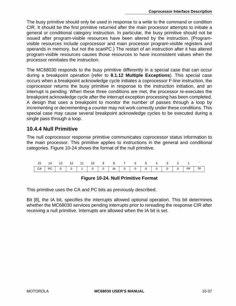
Coprocessor Interface Description
MOTOROLA MC68030 USER’S MANUAL 10-37
The busy primitive should only be used in response to a write to the command or conditionCIR. It should be the first primitive returned after the main processor attempts to initiate ageneral or conditional category instruction. In particular, the busy primitive should not beissued after program-visible resources have been altered by the instruction. (Program-visible resources include coprocessor and main processor program-visible registers andoperands in memory, but not the scanPC.) The restart of an instruction after it has alteredprogram-visible resources causes those resources to have inconsistent values when theprocessor reinitiates the instruction.
The MC68030 responds to the busy primitive differently in a special case that can occurduring a breakpoint operation (refer to 8.1.12 Multiple Exceptions). This special caseoccurs when a breakpoint acknowledge cycle initiates a coprocessor F-line instruction, thecoprocessor returns the busy primitive in response to the instruction initiation, and aninterrupt is pending. When these three conditions are met, the processor re-executes thebreakpoint acknowledge cycle after the interrupt exception processing has been completed.A design that uses a breakpoint to monitor the number of passes through a loop byincrementing or decrementing a counter may not work correctly under these conditions. Thisspecial case may cause several breakpoint acknowledge cycles to be executed during asingle pass through a loop.
10.4.4 Null PrimitiveThe null coprocessor response primitive communicates coprocessor status information tothe main processor. This primitive applies to instructions in the general and conditionalcategories. Figure 10-24 shows the format of the null primitive.
Figure 10-24. Null Primitive Format
This primitive uses the CA and PC bits as previously described.
Bit [8], the IA bit, specifies the interrupts allowed optional operation. This bit determineswhether the MC68030 services pending interrupts prior to rereading the response CIR afterreceiving a null primitive. Interrupts are allowed when the IA bit is set.
15 14 13 12 11 10 9 8 7 6 5 4 3 2 1 `
CA PC 0 0 1 0 0 IA 0 0 0 0 0 0 PF TF

Coprocessor Interface Description
10-38 MC68030 USER’S MANUAL MOTOROLA
Bit [1], the PF bit, shows the “processing finished”status of the coprocessor. That is, PF=1indicates that the coprocessor has completed all processing associated with an instruction.
Bit [0], the TF bit, indicates the true/false condition during the execution of a conditionalcategory instruction. TF=1 is the true condition specifier, and TF=0 is the false conditionspecifier. The TF bit is only relevant for null primitives with CA=0 that are used by thecoprocessor during the execution of a conditional instruction.
The MC68030 processes a null primitive with CA=1 in the same manner whether executinga general or conditional category coprocessor instruction. If the coprocessor sets CA and IAto one in the null primitive, the main processor services pending interrupts (using a mid-instruction stack frame, refer to Figure 10-43) and reads the response CIR again. If thecoprocessor sets CA to one and IA to zero in the null primitive, the main processor readsthe response CIR again without servicing any pending interrupts.
A null, CA=0 primitive provides a condition evaluation indicator to the main processor duringthe execution of a conditional instruction and ends the dialogue between the main processorand coprocessor for that instruction. The main processor completes the execution of aconditional category coprocessor instruction when it receives the primitive. The PF bit is notrelevant during conditional instruction execution since the primitive itself implies completionof processing.
Usually, when the main processor reads any primitive that does not have CA=1 whileexecuting a general category instruction, it terminates the dialogue between the mainprocessor and coprocessor. If a trace exception is pending, however, the main processordoes not terminate the instruction dialogue until it reads a null, CA=0, PF=1 primitive fromthe response CIR (refer to 10.5.2.5 Trace Exceptions). Thus, the main processor continuesto read the response CIR until it receives a null, CA=0, PF=1 primitive, and then performstrace exception processing. When IA=1, the main processor services pending interruptsbefore reading the response CIR again.

Coprocessor Interface Description
MOTOROLA MC68030 USER’S MANUAL 10-39
A coprocessor can be designed to execute a cpGEN instruction concurrently with theexecution of main processor instructions and, also, buffer one write operation to either itscommand or condition CIR. This type of coprocessor issues a null primitive with CA=1 whenit is concurrently executing a cpGEN instruction, and the main processor initiates anothergeneral or conditional coprocessor instruction. This primitive indicates that the coprocessoris busy and the main processor should read the response CIR again without reinitiating theinstruction. The IA bit of this null primitive usually should be set to minimize interrupt latencywhile the main processor is waiting for the coprocessor to complete the general categoryinstruction.
Table 10-3 summarizes the encodings of the null primitive.
x = Don't Carec = 1 or 0 Depending on Coprocessor Condition Evaluation
Table 10-3. Null Coprocessor Response Primitive Encodings
CA PC IA PF TF General Instructions Conditional Instructionsx 1 x x x Pass Program Counter to Instruction
Address CIR, Clear PC Bit, and Proceed with Operation Specified by CA, IA, PF, and TF Bits
Same as General Category
1 0 0 x x Reread Response CIR, Do Not Service Pending Interrupts
Same as General Category
1 0 1 x x Service Pending Interrupts and Reread the Response CIR
Same as General Category
0 0 0 0 c If (Trace Pending) Reread Response CIR; Else, Execute Next Instruction
Main Processor Completes Instruction Execution Based on TF=c.
0 0 1 0 c If (Trace Pending) Service Pending Interrupts and Reread Response CIR; Else, Execute Next Instruction
Main Processor Completes Instruction Execution Based on TF=c.
0 0 x 1 c Coprocessor Instruction Completed; Service Pending Exceptions or Execute Next Instruction
Main Processor Completes Instruction Execution Based on TF=c.

Coprocessor Interface Description
10-40 MC68030 USER’S MANUAL MOTOROLA
10.4.5 Supervisor Check PrimitiveThe supervisor check primitive verifies that the main processor is operating in the supervisorstate while executing a coprocessor instruction. This primitive applies to instructions in thegeneral and conditional coprocessor instruction categories. Figure 10-25 shows the formatof the supervisor check primitive.
Figure 10-25. Supervisor Check Primitive Format
This primitive uses the PC bit as previously described. Bit [15] is shown as one, but duringexecution of a general category instruction, this primitive performs the same operationsregardless of the value of bit [15]. If this primitive is issued with bit [15]=0 during a conditionalcategory instruction, however, the main processor initiates protocol violation exceptionprocessing.
When the main processor reads the supervisor check primitive from the response CIR, itchecks the value of the S bit in the status register. If S=0 (main processor operating at userprivilege level), the main processor aborts the coprocessor instruction by writing an abortmask (refer to 10.3.2 Control CIR) to the control CIR. The main processor then initiatesprivilege violation exception processing (refer to 10.5.2.3 Privilege Violations). If the mainprocessor is at the supervisor privilege level when it receives this primitive, it reads theresponse CIR again.
The supervisor check primitive allows privileged instructions to be defined in thecoprocessor general and conditional instruction categories. This primitive should be the firstone issued by the coprocessor during the dialog for an instruction that is implemented asprivileged.
10.4.6 Transfer Operation Word PrimitiveThe transfer operation word primitive requests a copy of the coprocessor instructionoperation word for the coprocessor. This primitive applies to general and conditionalcategory instructions. Figure 10-26 shows the format of the transfer operation wordprimitive.
15 14 13 12 11 10 9 8 7 6 5 4 3 2 1 0
1 PC 0 0 0 1 0 0 0 0 0 0 0 0 0 0
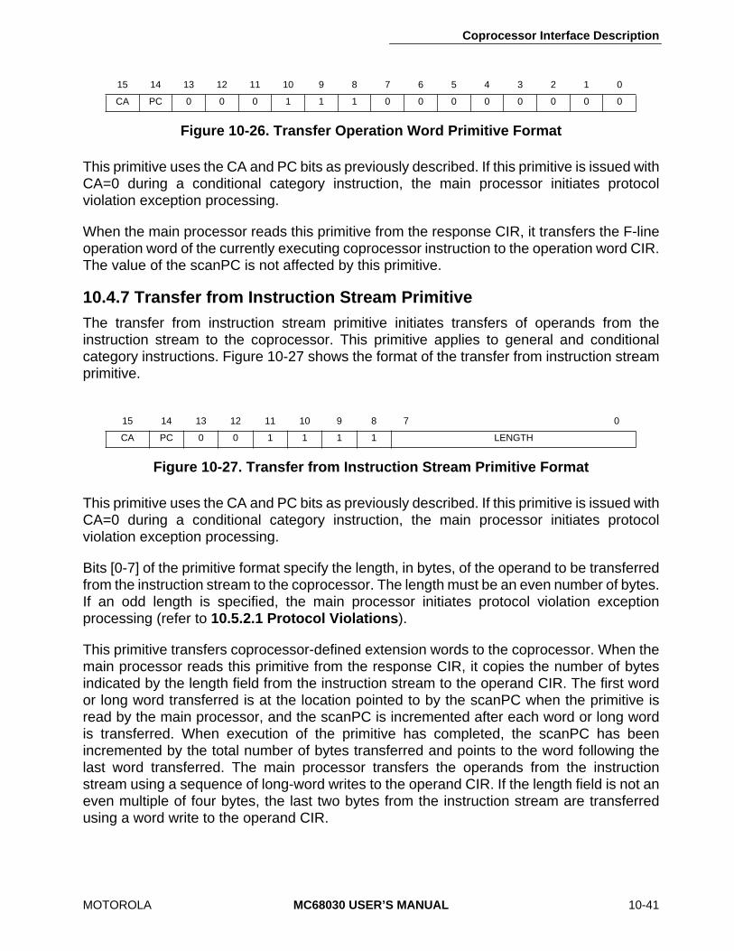
Coprocessor Interface Description
MOTOROLA MC68030 USER’S MANUAL 10-41
Figure 10-26. Transfer Operation Word Primitive Format
This primitive uses the CA and PC bits as previously described. If this primitive is issued withCA=0 during a conditional category instruction, the main processor initiates protocolviolation exception processing.
When the main processor reads this primitive from the response CIR, it transfers the F-lineoperation word of the currently executing coprocessor instruction to the operation word CIR.The value of the scanPC is not affected by this primitive.
10.4.7 Transfer from Instruction Stream PrimitiveThe transfer from instruction stream primitive initiates transfers of operands from theinstruction stream to the coprocessor. This primitive applies to general and conditionalcategory instructions. Figure 10-27 shows the format of the transfer from instruction streamprimitive.
Figure 10-27. Transfer from Instruction Stream Primitive Format
This primitive uses the CA and PC bits as previously described. If this primitive is issued withCA=0 during a conditional category instruction, the main processor initiates protocolviolation exception processing.
Bits [0-7] of the primitive format specify the length, in bytes, of the operand to be transferredfrom the instruction stream to the coprocessor. The length must be an even number of bytes.If an odd length is specified, the main processor initiates protocol violation exceptionprocessing (refer to 10.5.2.1 Protocol Violations).
This primitive transfers coprocessor-defined extension words to the coprocessor. When themain processor reads this primitive from the response CIR, it copies the number of bytesindicated by the length field from the instruction stream to the operand CIR. The first wordor long word transferred is at the location pointed to by the scanPC when the primitive isread by the main processor, and the scanPC is incremented after each word or long wordis transferred. When execution of the primitive has completed, the scanPC has beenincremented by the total number of bytes transferred and points to the word following thelast word transferred. The main processor transfers the operands from the instructionstream using a sequence of long-word writes to the operand CIR. If the length field is not aneven multiple of four bytes, the last two bytes from the instruction stream are transferredusing a word write to the operand CIR.
15 14 13 12 11 10 9 8 7 6 5 4 3 2 1 0
CA PC 0 0 0 1 1 1 0 0 0 0 0 0 0 0
15 14 13 12 11 10 9 8 7 0
CA PC 0 0 1 1 1 1 LENGTH
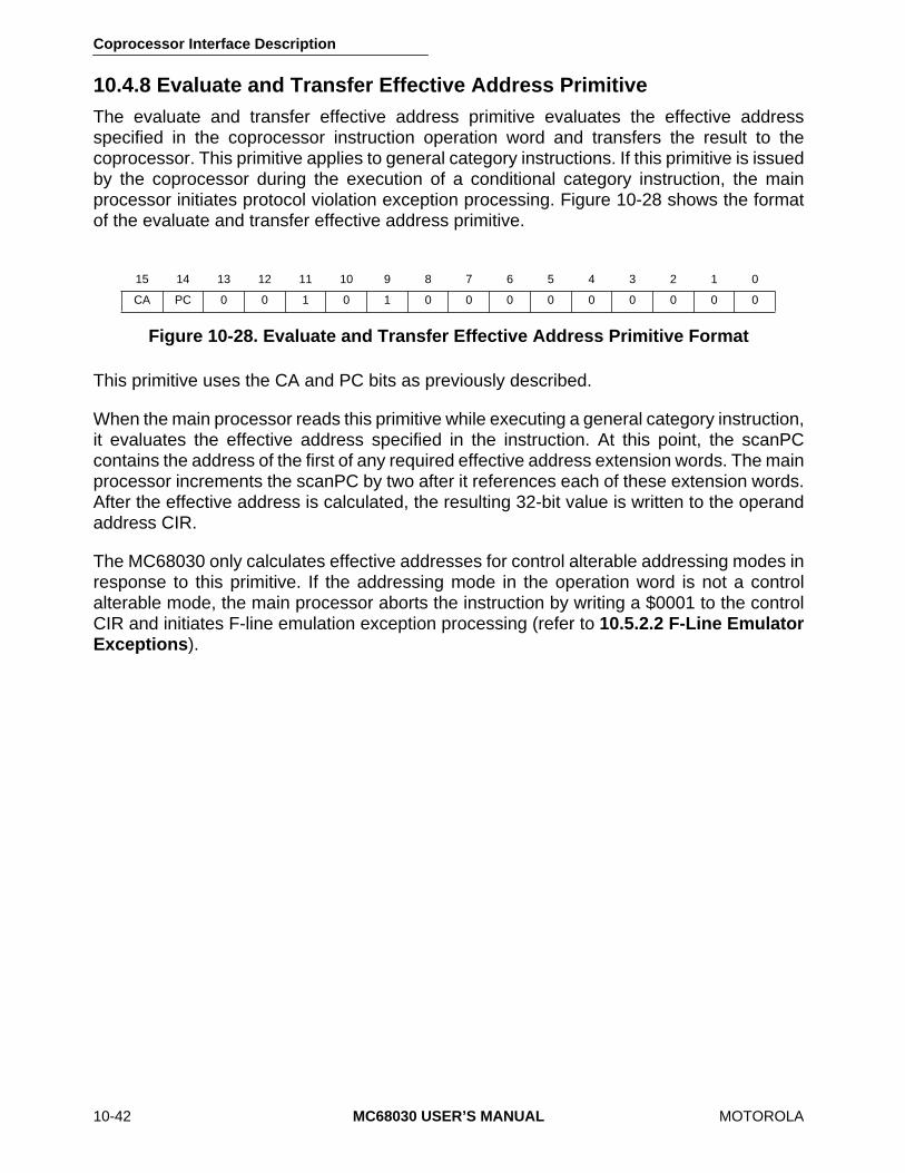
Coprocessor Interface Description
10-42 MC68030 USER’S MANUAL MOTOROLA
10.4.8 Evaluate and Transfer Effective Address PrimitiveThe evaluate and transfer effective address primitive evaluates the effective addressspecified in the coprocessor instruction operation word and transfers the result to thecoprocessor. This primitive applies to general category instructions. If this primitive is issuedby the coprocessor during the execution of a conditional category instruction, the mainprocessor initiates protocol violation exception processing. Figure 10-28 shows the formatof the evaluate and transfer effective address primitive.
Figure 10-28. Evaluate and Transfer Effective Address Primitive Format
This primitive uses the CA and PC bits as previously described.
When the main processor reads this primitive while executing a general category instruction,it evaluates the effective address specified in the instruction. At this point, the scanPCcontains the address of the first of any required effective address extension words. The mainprocessor increments the scanPC by two after it references each of these extension words.After the effective address is calculated, the resulting 32-bit value is written to the operandaddress CIR.
The MC68030 only calculates effective addresses for control alterable addressing modes inresponse to this primitive. If the addressing mode in the operation word is not a controlalterable mode, the main processor aborts the instruction by writing a $0001 to the controlCIR and initiates F-line emulation exception processing (refer to 10.5.2.2 F-Line EmulatorExceptions).
15 14 13 12 11 10 9 8 7 6 5 4 3 2 1 0
CA PC 0 0 1 0 1 0 0 0 0 0 0 0 0 0
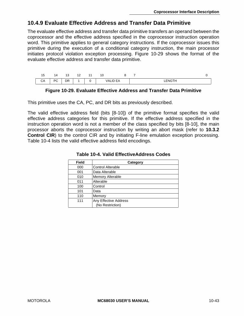
Coprocessor Interface Description
MOTOROLA MC68030 USER’S MANUAL 10-43
10.4.9 Evaluate Effective Address and Transfer Data PrimitiveThe evaluate effective address and transfer data primitive transfers an operand between thecoprocessor and the effective address specified in the coprocessor instruction operationword. This primitive applies to general category instructions. If the coprocessor issues thisprimitive during the execution of a conditional category instruction, the main processorinitiates protocol violation exception processing. Figure 10-29 shows the format of theevaluate effective address and transfer data primitive.
Figure 10-29. Evaluate Effective Address and Transfer Data Primitive
This primitive uses the CA, PC, and DR bits as previously described.
The valid effective address field (bits [8-10]) of the primitive format specifies the valideffective address categories for this primitive. If the effective address specified in theinstruction operation word is not a member of the class specified by bits [8-10], the mainprocessor aborts the coprocessor instruction by writing an abort mask (refer to 10.3.2Control CIR) to the control CIR and by initiating F-line emulation exception processing.Table 10-4 lists the valid effective address field encodings.
15 14 13 12 11 10 8 7 0
CA PC DR 1 0 VALID EA LENGTH
Table 10-4. Valid EffectiveAddress Codes
Field Category000 Control Alterable001 Data Alterable010 Memory Alterable011 Alterable100 Control101 Data110 Memory111 Any Effective Address
(No Restriction)
Coprocessor Interface Description
10-44 MC68030 USER’S MANUAL MOTOROLA
Even when the valid effective address fields specified in the primitive and in the instructionoperation word match, the MC68030 initiates protocol violation exception processing if theprimitive requests a write to a nonalterable effective address.
The length in bytes of the operand to be transferred is specified by bits [0-7] of the primitiveformat. Several restrictions apply to operand lengths for certain effective addressing modes.If the effective address is a main processor register (register direct mode), only operandlengths of one, two, or four bytes are valid; all other lengths (zero, for example) cause themain processor to initiate protocol violation exception processing. Operand lengths of 0-255bytes are valid for the memory addressing modes.
The length of 0-255 bytes does not apply to an immediate operand. The length of animmediate operand must be one byte or an even number of bytes (less than 256), and thedirection of transfer must be to the coprocessor; otherwise, the main processor initiatesprotocol violation exception processing.
When the main processor receives this primitive during the execution of a general categoryinstruction, it verifies that the effective address encoded in the instruction operation word isin the category specified by the primitive. If so, the processor calculates the effectiveaddress using the appropriate effective address extension words at the current scanPCaddress and increments the scanPC by two for each word referenced. The main processorthen transfers the number of bytes specified in the primitive between the operand CIR andthe effective address using long-word transfers whenever possible. Refer to 10.3.8Operand CIR for information concerning operand alignment for transfers involving theoperand CIR.
The DR bit specifies the direction of the operand transfer. DR=0 requests a transfer from theeffective address to the operand CIR, and DR=1 specifies a transfer from the operand CIRto the effective address.
Coprocessor Interface Description
MOTOROLA MC68030 USER’S MANUAL 10-45
If the effective addressing mode specifies the predecrement mode, the address registerused is decremented by the size of the operand before the transfer. The bytes within theoperand are then transferred to or from ascending addresses beginning with the locationspecified by the decremented address register. In this mode, if A7 is used as the addressregister and the operand length is one byte, A7 is decremented by two to maintain a word-aligned stack.
For the postincrement effective addressing mode, the address register used is incrementedby the size of the operand after the transfer. The bytes within the operand are transferred toor from ascending addresses beginning with the location specified by the address register.In this mode, if A7 is used as the address register and the operand length is one byte, A7 isincremented by two after the transfer to maintain a word aligned stack. Transferring oddlength operands longer than one byte using the –(A7) or (A7)+ addressing modes can resultin a stack pointer that is not word aligned.
The processor repeats the effective address calculation each time this primitive is issuedduring the execution of a given instruction. The calculation uses the current contents of anyrequired address and data registers. The instruction must include a set of effective addressextension words for each repetition of a calculation that requires them. The processorlocates these words at the current scanPC location and increments the scanPC by two foreach word referenced in the instruction stream.
The MC68030 sign-extends a byte or word-sized operand to a long-word value when it istransferred to an address register (A0–A7) using this primitive with the register directeffective addressing mode. A byte or word-sized operand transferred to a data register (D0–D7) only overwrites the lower byte or word of the data register.

Coprocessor Interface Description
10-46 MC68030 USER’S MANUAL MOTOROLA
10.4.10 Write to Previously Evaluated Effective Address PrimitiveThe write to previously evaluated effective address primitive transfers an operand from thecoprocessor to a previously evaluated effective address. This primitive applies to generalcategory instructions. If the coprocessor uses this primitive during the execution of aconditional category instruction, the main processor initiates protocol violation exceptionprocessing. Figure 10-30 shows the format of the write to previously evaluated effectiveaddress primitive.
Figure 10-30. Write to Previously Evaluated EffectiveAddress Primitive Format
This primitive uses the CA and PC bits as previously described.
Bits [0-7] of the primitive format specify the length of the operand in bytes. The MC68030transfers operands between zero and 255 bytes in length.
When the main processor receives this primitive during the execution of a general categoryinstruction, it transfers an operand from the operand CIR to an effective address specifiedby a temporary register within the MC68030. When a previous primitive for the currentinstruction has evaluated the effective address, this temporary register contains theevaluated effective address. Primitives that store an evaluated effective address in atemporary register of the main processor are the evaluate and transfer effective address,evaluate effective address and transfer data, and transfer multiple coprocessor registersprimitive. If this primitive is used during an instruction in which the effective addressspecified in the instruction operation word has not been calculated, the effective addressused for the write is undefined. Also, if the previously evaluated effective address wasregister direct, the address written to in response to this primitive is undefined.
The function code value during the write operation indicates either supervisor or user dataspace, depending on the value of the S bit in the MC68030 status register when theprocessor reads this primitive. While a coprocessor should request writes to only alterableeffective addressing modes, the MC68030 does not check the type of effective addressused with this primitive. For example, if the previously evaluated effective address wasprogram counter relative and the MC68030 is at the user privilege level (S=0 in statusregister), the MC68030 writes to user data space at the previously calculated programrelative address (the 32-bit value in the temporary internal register of the processor).
15 14 13 12 11 10 9 8 7 0
CA PC 1 0 0 0 0 0 LENGTH

Coprocessor Interface Description
MOTOROLA MC68030 USER’S MANUAL 10-47
Operands longer than four bytes are transferred in increments of four bytes (operand parts)when possible. The main processor reads a long-word operand part from the operand CIRand transfers this part to the current effective address. The transfers continue in this mannerusing ascending memory locations until all of the long-word operand parts are transferred,and any remaining operand part is then transferred using a one-, two-, or three-byte transferas required. The operand parts are stored in memory using ascending addresses beginningwith the address in the MC68030 temporary register.
The execution of this primitive does not modify any of the registers in the MC68030programmer's model, even if the previously evaluated effective address mode is thepredecrement or postincrement mode. If the previously evaluated effective addressingmode used any of the MC68030 internal address or data registers, the effective addressvalue used is the final value from the preceding primitive. That is, this primitive uses thevalue from an evaluate and transfer effective address, evaluate effective address andtransfer data, or transfer multiple coprocessor registers primitive without modification.
The take address and transfer data primitive described in the next section does not replacethe effective address value that has been calculated by the MC68030. The address that themain processor obtains in response to the take address and transfer data primitive is notavailable to the write to previously evaluated effective address primitive.
A coprocessor can issue an evaluate effective address and transfer data primitive followedby this primitive to perform a read-modify-write operation that is not indivisible. The buscycles for this operation are normal bus cycles that can be interrupted, and the bus can bearbitrated between the cycles.
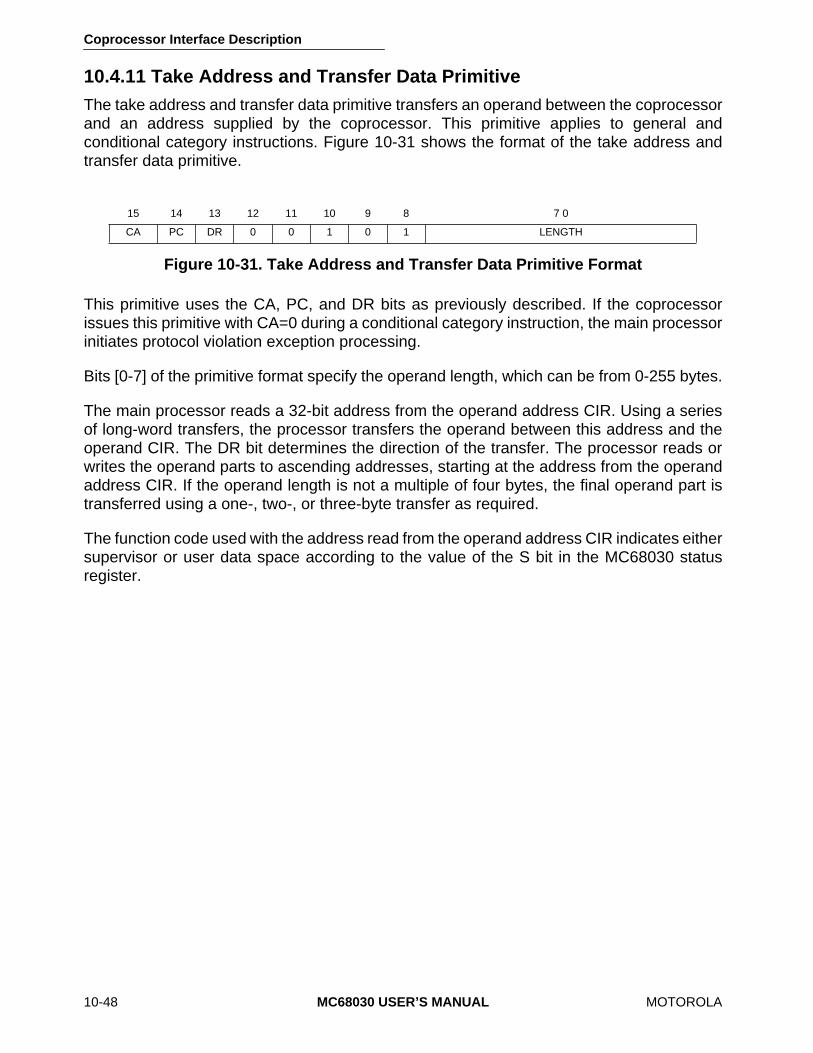
Coprocessor Interface Description
10-48 MC68030 USER’S MANUAL MOTOROLA
10.4.11 Take Address and Transfer Data PrimitiveThe take address and transfer data primitive transfers an operand between the coprocessorand an address supplied by the coprocessor. This primitive applies to general andconditional category instructions. Figure 10-31 shows the format of the take address andtransfer data primitive.
Figure 10-31. Take Address and Transfer Data Primitive Format
This primitive uses the CA, PC, and DR bits as previously described. If the coprocessorissues this primitive with CA=0 during a conditional category instruction, the main processorinitiates protocol violation exception processing.
Bits [0-7] of the primitive format specify the operand length, which can be from 0-255 bytes.
The main processor reads a 32-bit address from the operand address CIR. Using a seriesof long-word transfers, the processor transfers the operand between this address and theoperand CIR. The DR bit determines the direction of the transfer. The processor reads orwrites the operand parts to ascending addresses, starting at the address from the operandaddress CIR. If the operand length is not a multiple of four bytes, the final operand part istransferred using a one-, two-, or three-byte transfer as required.
The function code used with the address read from the operand address CIR indicates eithersupervisor or user data space according to the value of the S bit in the MC68030 statusregister.
15 14 13 12 11 10 9 8 7 0
CA PC DR 0 0 1 0 1 LENGTH
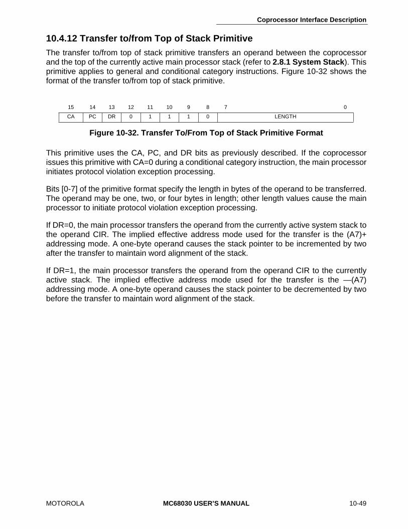
Coprocessor Interface Description
MOTOROLA MC68030 USER’S MANUAL 10-49
10.4.12 Transfer to/from Top of Stack PrimitiveThe transfer to/from top of stack primitive transfers an operand between the coprocessorand the top of the currently active main processor stack (refer to 2.8.1 System Stack). Thisprimitive applies to general and conditional category instructions. Figure 10-32 shows theformat of the transfer to/from top of stack primitive.
Figure 10-32. Transfer To/From Top of Stack Primitive Format
This primitive uses the CA, PC, and DR bits as previously described. If the coprocessorissues this primitive with CA=0 during a conditional category instruction, the main processorinitiates protocol violation exception processing.
Bits [0-7] of the primitive format specify the length in bytes of the operand to be transferred.The operand may be one, two, or four bytes in length; other length values cause the mainprocessor to initiate protocol violation exception processing.
If DR=0, the main processor transfers the operand from the currently active system stack tothe operand CIR. The implied effective address mode used for the transfer is the (A7)+addressing mode. A one-byte operand causes the stack pointer to be incremented by twoafter the transfer to maintain word alignment of the stack.
If DR=1, the main processor transfers the operand from the operand CIR to the currentlyactive stack. The implied effective address mode used for the transfer is the —(A7)addressing mode. A one-byte operand causes the stack pointer to be decremented by twobefore the transfer to maintain word alignment of the stack.
15 14 13 12 11 10 9 8 7 0
CA PC DR 0 1 1 1 0 LENGTH

Coprocessor Interface Description
10-50 MC68030 USER’S MANUAL MOTOROLA
10.4.13 Transfer Single Main Processor Register PrimitiveThe transfer single main processor register primitive transfers an operand between one ofthe main processor's data or address registers and the coprocessor. This primitive appliesto general and conditional category instructions. Figure 10-33 shows the format of thetransfer single main processor register primitive.
Figure 10-33. Transfer Single Main Processor Register Primitive Format
This primitive uses the CA, PC, and DR bits as previously described. If the coprocessorissues this primitive with CA=0 during a conditional category instruction, the main processorinitiates protocol violation exception processing.
Bit [3], the D/A bit, specifies whether the primitive transfers an address or data register. D/A=0 indicates a data register, and D/A=1 indicates an address register. Bits [2-0] contain theregister number.
If DR=0, the main processor writes the long-word operand in the specified register to theoperand CIR. If DR=1, the main processor reads a long-word operand from the operand CIRand transfers it to the specified data or address register.
10.4.14 Transfer Main Processor Control Register PrimitiveThe transfer main processor control register primitive transfers a long-word operandbetween one of its control registers and the coprocessor. This primitive applies to generaland conditional category instructions. Figure 10-34 shows the format of the transfer mainprocessor control register primitive. This primitive uses the CA, PC, and DR bits aspreviously described. If the coprocessor issues this primitive with CA=0 during a conditionalcategory instruction, the main processor initiates protocol violation exception processing.
15 14 13 12 11 10 9 8 7 6 5 4 3 2 0
CA PC DR 0 1 1 0 0 0 0 0 0 D/A REGISTER

Coprocessor Interface Description
MOTOROLA MC68030 USER’S MANUAL 10-51
Figure 10-34. Transfer Main Processor Control Register Primitive Format
When the main processor receives this primitive, it reads a control register select code fromthe register select CIR. This code determines which main processor control register istransferred. Table 10-5 lists the valid control register select codes. If the control registerselect code is not valid, the MC68030 initiates protocol violation exception processing (referto 10.5.2.1 Protocol Violations).
After reading a valid code from the register select CIR, if DR=0, the main processor writesthe long-word operand from the specified control register to the operand CIR. If DR=1, themain processor reads a long-word operand from the operand CIR and places it in thespecified control register.
15 14 13 12 11 10 9 8 7 6 5 4 3 2 1 0
CA PC DR 0 1 1 0 1 0 0 0 0 0 0 0 0
Table 10-5. Main Processor Control Register
Hex Control Registerx000 Source Function Code (SFC) Registerx001 Destination Function Code (DFC) Registerx002 Cache Control Register (CACR)x800 User Stack Pointer (USP)x801 Vector Base Register (VBR)x802 Cache Address Register (CAAR)x803 Master Stack Pointer (MSP)x804 Interrupt Stack Pointer (ISP)
All other codes cause a protocol violation exception
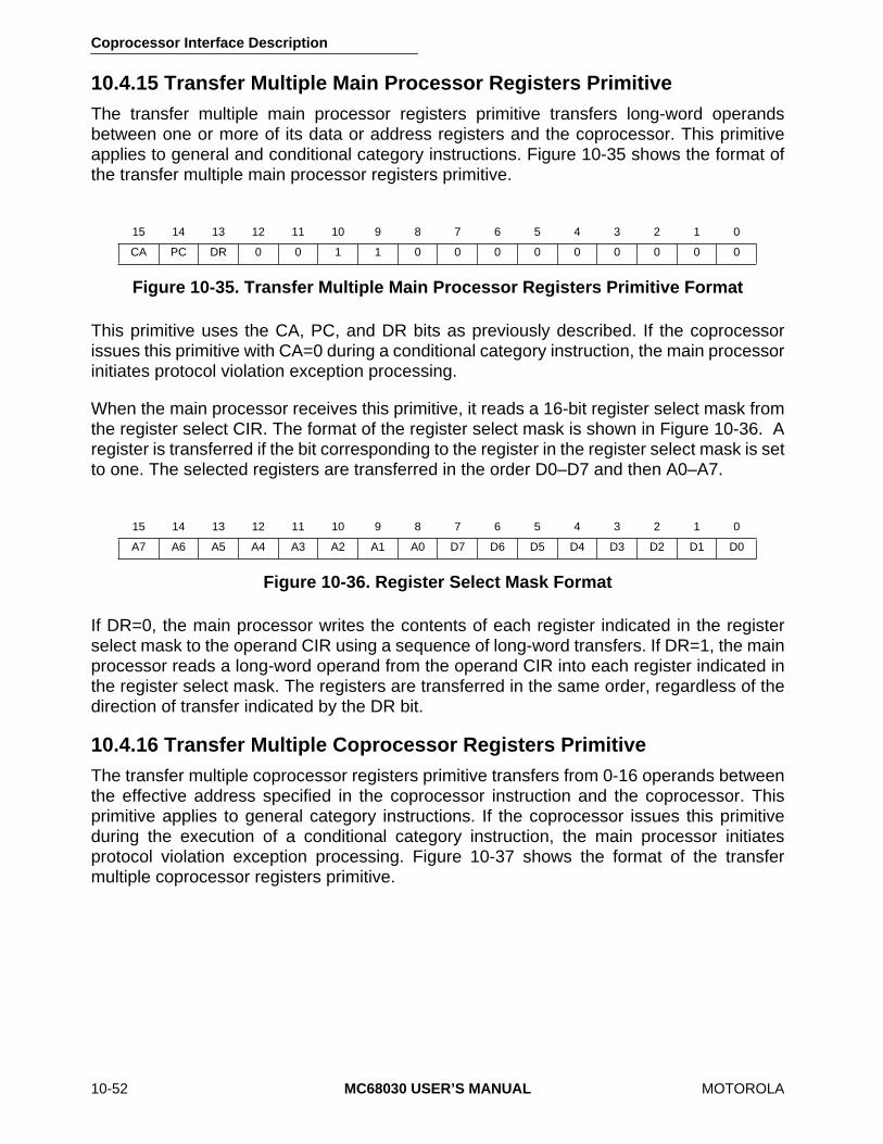
Coprocessor Interface Description
10-52 MC68030 USER’S MANUAL MOTOROLA
10.4.15 Transfer Multiple Main Processor Registers PrimitiveThe transfer multiple main processor registers primitive transfers long-word operandsbetween one or more of its data or address registers and the coprocessor. This primitiveapplies to general and conditional category instructions. Figure 10-35 shows the format ofthe transfer multiple main processor registers primitive.
Figure 10-35. Transfer Multiple Main Processor Registers Primitive Format
This primitive uses the CA, PC, and DR bits as previously described. If the coprocessorissues this primitive with CA=0 during a conditional category instruction, the main processorinitiates protocol violation exception processing.
When the main processor receives this primitive, it reads a 16-bit register select mask fromthe register select CIR. The format of the register select mask is shown in Figure 10-36. Aregister is transferred if the bit corresponding to the register in the register select mask is setto one. The selected registers are transferred in the order D0–D7 and then A0–A7.
Figure 10-36. Register Select Mask Format
If DR=0, the main processor writes the contents of each register indicated in the registerselect mask to the operand CIR using a sequence of long-word transfers. If DR=1, the mainprocessor reads a long-word operand from the operand CIR into each register indicated inthe register select mask. The registers are transferred in the same order, regardless of thedirection of transfer indicated by the DR bit.
10.4.16 Transfer Multiple Coprocessor Registers PrimitiveThe transfer multiple coprocessor registers primitive transfers from 0-16 operands betweenthe effective address specified in the coprocessor instruction and the coprocessor. Thisprimitive applies to general category instructions. If the coprocessor issues this primitiveduring the execution of a conditional category instruction, the main processor initiatesprotocol violation exception processing. Figure 10-37 shows the format of the transfermultiple coprocessor registers primitive.
15 14 13 12 11 10 9 8 7 6 5 4 3 2 1 0
CA PC DR 0 0 1 1 0 0 0 0 0 0 0 0 0
15 14 13 12 11 10 9 8 7 6 5 4 3 2 1 0
A7 A6 A5 A4 A3 A2 A1 A0 D7 D6 D5 D4 D3 D2 D1 D0
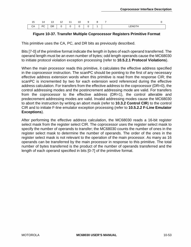
Coprocessor Interface Description
MOTOROLA MC68030 USER’S MANUAL 10-53
Figure 10-37. Transfer Multiple Coprocessor Registers Primitive Format
This primitive uses the CA, PC, and DR bits as previously described.
Bits [7-0] of the primitive format indicate the length in bytes of each operand transferred. Theoperand length must be an even number of bytes; odd length operands cause the MC68030to initiate protocol violation exception processing (refer to 10.5.2.1 Protocol Violations).
When the main processor reads this primitive, it calculates the effective address specifiedin the coprocessor instruction. The scanPC should be pointing to the first of any necessaryeffective address extension words when this primitive is read from the response CIR; thescanPC is incremented by two for each extension word referenced during the effectiveaddress calculation. For transfers from the effective address to the coprocessor (DR=0), thecontrol addressing modes and the postincrement addressing mode are valid. For transfersfrom the coprocessor to the effective address (DR=1), the control alterable andpredecrement addressing modes are valid. Invalid addressing modes cause the MC68030to abort the instruction by writing an abort mask (refer to 10.3.2 Control CIR) to the controlCIR and to initiate F-line emulator exception processing (refer to 10.5.2.2 F-Line EmulatorExceptions).
After performing the effective address calculation, the MC68030 reads a 16-bit registerselect mask from the register select CIR. The coprocessor uses the register select mask tospecify the number of operands to transfer; the MC68030 counts the number of ones in theregister select mask to determine the number of operands. The order of the ones in theregister select mask is not relevant to the operation of the main processor. As many as 16operands can be transferred by the main processor in response to this primitive. The totalnumber of bytes transferred is the product of the number of operands transferred and thelength of each operand specified in bits [0-7] of the primitive format.
15 14 13 12 11 10 9 8 7 0
CA PC DR 0 0 0 0 1 LENGTH

Coprocessor Interface Description
10-54 MC68030 USER’S MANUAL MOTOROLA
If DR=1, the main processor reads the number of operands specified in the register selectmask from the operand CIR and writes these operands to the effective address specified inthe instruction using long-word transfers whenever possible. If DR=0, the main processorreads the number of operands specified in the register select mask from the effectiveaddress and writes them to the operand CIR.
For the control addressing modes, the operands are transferred to or from memory usingascending addresses. For the postincrement addressing mode, the operands are read frommemory with ascending addresses also, and the address register used is incremented bythe size of an operand after each operand is transferred. The address register used with the(An)+ addressing mode is incremented by the total number of bytes transferred during theprimitive execution.
For the predecrement addressing mode, the operands are written to memory withdescending addresses, but the bytes within each operand are written to memory withascending addresses. As an example, Figure 10-38 shows the format in long-word-orientedmemory for two 12-byte operands transferred from the coprocessor to the effective addressusing the —(An) addressing mode. The processor decrements the address register by thesize of an operand before the operand is transferred. It writes the bytes of the operand toascending memory addresses. When the transfer is complete, the address register hasbeen decremented by the total number of bytes transferred. The MC68030 transfers thedata using long-word transfers whenever possible.
NOTE: OP0, Byte (0) is the first byte written to memoryOP0, Byte (L-1) is the last byte of the first operand written to memoryOP1, Byte (0) is the first byte of the second operand written to memoryOP1, Byte (L-1) is the last byte written to memory
Figure 10-38. Operand Format in Memory for Transfer to —(An)
31 23 15 7 0An-2•LENGTH=FINAL An → OP1, BYTE (0)
OP1, BYTE (L-1)An-LENGTH → OP0, BYTE (0)
INITIAL An → OP0, BYTE (L-1)
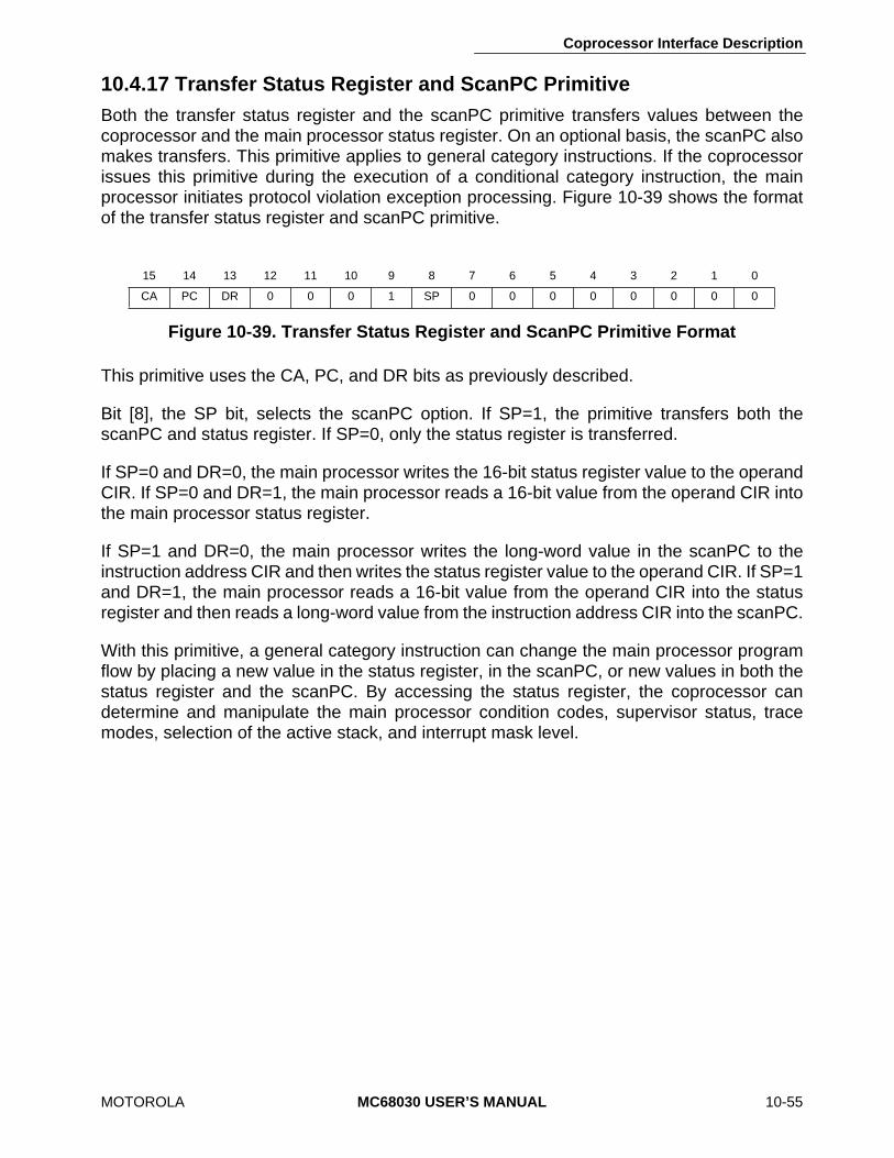
Coprocessor Interface Description
MOTOROLA MC68030 USER’S MANUAL 10-55
10.4.17 Transfer Status Register and ScanPC PrimitiveBoth the transfer status register and the scanPC primitive transfers values between thecoprocessor and the main processor status register. On an optional basis, the scanPC alsomakes transfers. This primitive applies to general category instructions. If the coprocessorissues this primitive during the execution of a conditional category instruction, the mainprocessor initiates protocol violation exception processing. Figure 10-39 shows the formatof the transfer status register and scanPC primitive.
Figure 10-39. Transfer Status Register and ScanPC Primitive Format
This primitive uses the CA, PC, and DR bits as previously described.
Bit [8], the SP bit, selects the scanPC option. If SP=1, the primitive transfers both thescanPC and status register. If SP=0, only the status register is transferred.
If SP=0 and DR=0, the main processor writes the 16-bit status register value to the operandCIR. If SP=0 and DR=1, the main processor reads a 16-bit value from the operand CIR intothe main processor status register.
If SP=1 and DR=0, the main processor writes the long-word value in the scanPC to theinstruction address CIR and then writes the status register value to the operand CIR. If SP=1and DR=1, the main processor reads a 16-bit value from the operand CIR into the statusregister and then reads a long-word value from the instruction address CIR into the scanPC.
With this primitive, a general category instruction can change the main processor programflow by placing a new value in the status register, in the scanPC, or new values in both thestatus register and the scanPC. By accessing the status register, the coprocessor candetermine and manipulate the main processor condition codes, supervisor status, tracemodes, selection of the active stack, and interrupt mask level.
15 14 13 12 11 10 9 8 7 6 5 4 3 2 1 0
CA PC DR 0 0 0 1 SP 0 0 0 0 0 0 0 0
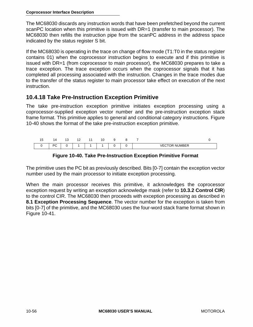
Coprocessor Interface Description
10-56 MC68030 USER’S MANUAL MOTOROLA
The MC68030 discards any instruction words that have been prefetched beyond the currentscanPC location when this primitive is issued with DR=1 (transfer to main processor). TheMC68030 then refills the instruction pipe from the scanPC address in the address spaceindicated by the status register S bit.
If the MC68030 is operating in the trace on change of flow mode (T1:T0 in the status registercontains 01) when the coprocessor instruction begins to execute and if this primitive isissued with DR=1 (from coprocessor to main processor), the MC68030 prepares to take atrace exception. The trace exception occurs when the coprocessor signals that it hascompleted all processing associated with the instruction. Changes in the trace modes dueto the transfer of the status register to main processor take effect on execution of the nextinstruction.
10.4.18 Take Pre-Instruction Exception PrimitiveThe take pre-instruction exception primitive initiates exception processing using acoprocessor-supplied exception vector number and the pre-instruction exception stackframe format. This primitive applies to general and conditional category instructions. Figure10-40 shows the format of the take pre-instruction exception primitive.
Figure 10-40. Take Pre-Instruction Exception Primitive Format
The primitive uses the PC bit as previously described. Bits [0-7] contain the exception vectornumber used by the main processor to initiate exception processing.
When the main processor receives this primitive, it acknowledges the coprocessorexception request by writing an exception acknowledge mask (refer to 10.3.2 Control CIR)to the control CIR. The MC68030 then proceeds with exception processing as described in8.1 Exception Processing Sequence. The vector number for the exception is taken frombits [0-7] of the primitive, and the MC68030 uses the four-word stack frame format shown inFigure 10-41.
15 14 13 12 11 10 9 8 7 0
0 PC 0 1 1 1 0 0 VECTOR NUMBER
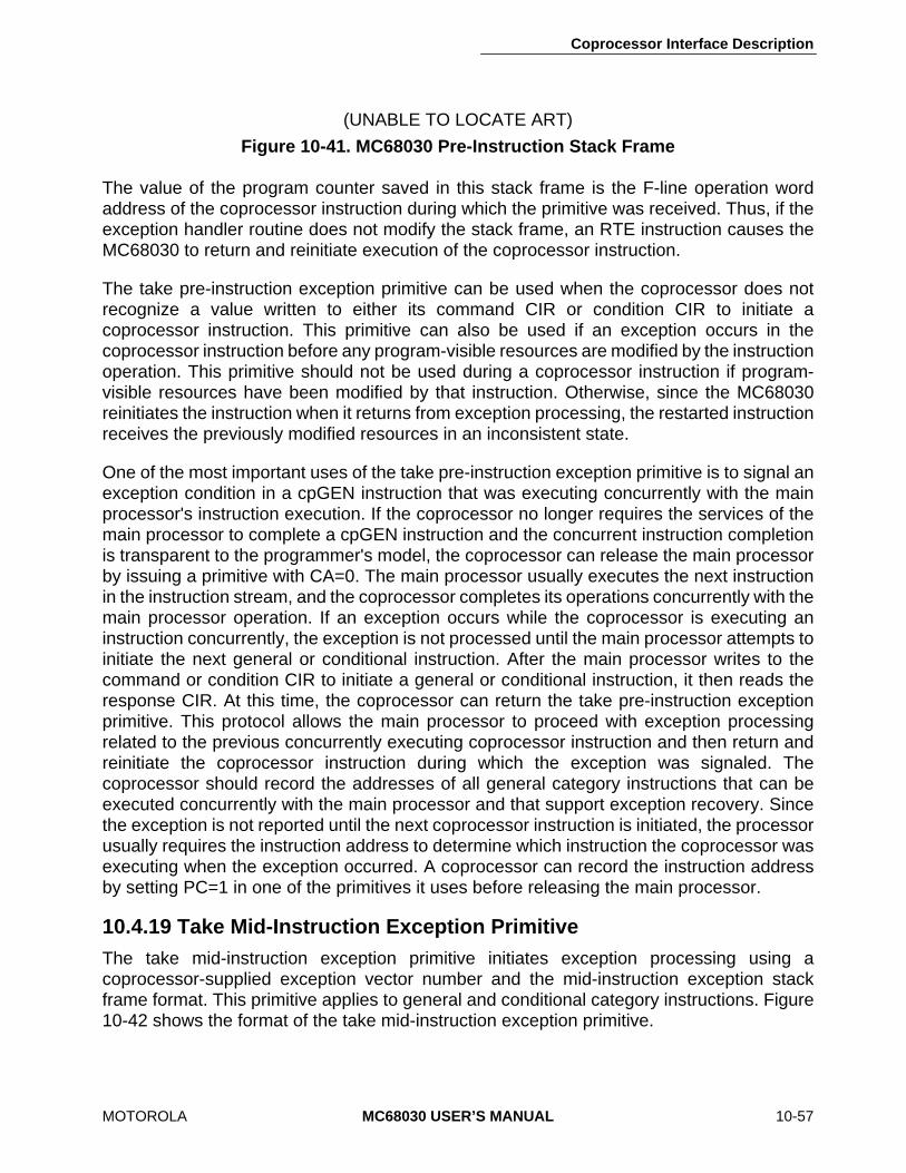
Coprocessor Interface Description
MOTOROLA MC68030 USER’S MANUAL 10-57
The value of the program counter saved in this stack frame is the F-line operation wordaddress of the coprocessor instruction during which the primitive was received. Thus, if theexception handler routine does not modify the stack frame, an RTE instruction causes theMC68030 to return and reinitiate execution of the coprocessor instruction.
The take pre-instruction exception primitive can be used when the coprocessor does notrecognize a value written to either its command CIR or condition CIR to initiate acoprocessor instruction. This primitive can also be used if an exception occurs in thecoprocessor instruction before any program-visible resources are modified by the instructionoperation. This primitive should not be used during a coprocessor instruction if program-visible resources have been modified by that instruction. Otherwise, since the MC68030reinitiates the instruction when it returns from exception processing, the restarted instructionreceives the previously modified resources in an inconsistent state.
One of the most important uses of the take pre-instruction exception primitive is to signal anexception condition in a cpGEN instruction that was executing concurrently with the mainprocessor's instruction execution. If the coprocessor no longer requires the services of themain processor to complete a cpGEN instruction and the concurrent instruction completionis transparent to the programmer's model, the coprocessor can release the main processorby issuing a primitive with CA=0. The main processor usually executes the next instructionin the instruction stream, and the coprocessor completes its operations concurrently with themain processor operation. If an exception occurs while the coprocessor is executing aninstruction concurrently, the exception is not processed until the main processor attempts toinitiate the next general or conditional instruction. After the main processor writes to thecommand or condition CIR to initiate a general or conditional instruction, it then reads theresponse CIR. At this time, the coprocessor can return the take pre-instruction exceptionprimitive. This protocol allows the main processor to proceed with exception processingrelated to the previous concurrently executing coprocessor instruction and then return andreinitiate the coprocessor instruction during which the exception was signaled. Thecoprocessor should record the addresses of all general category instructions that can beexecuted concurrently with the main processor and that support exception recovery. Sincethe exception is not reported until the next coprocessor instruction is initiated, the processorusually requires the instruction address to determine which instruction the coprocessor wasexecuting when the exception occurred. A coprocessor can record the instruction addressby setting PC=1 in one of the primitives it uses before releasing the main processor.
10.4.19 Take Mid-Instruction Exception PrimitiveThe take mid-instruction exception primitive initiates exception processing using acoprocessor-supplied exception vector number and the mid-instruction exception stackframe format. This primitive applies to general and conditional category instructions. Figure10-42 shows the format of the take mid-instruction exception primitive.
(UNABLE TO LOCATE ART)
Figure 10-41. MC68030 Pre-Instruction Stack Frame

Coprocessor Interface Description
10-58 MC68030 USER’S MANUAL MOTOROLA
Figure 10-42. Take Mid-Instruction Exception Primitive Format
This primitive uses the PC bit as previously described. Bits ;ob7-0] contain the exceptionvector number used by the main processor to initiate exception processing.
When the main processor receives this primitive, it acknowledges the coprocessorexception request by writing an exception acknowledge mask (refer to 10.3.2 Control CIR)to the control CIR. The MC68030 then performs exception processing as described in 8.1Exception Processing Sequence. The vector number for the exception is taken from bits[0-7] of the primitive and the MC68030 uses the 10-word stack frame format shown in Figure10-43.
15 14 13 12 11 10 9 8 7 0
0 PC 0 1 1 1 0 1 VECTOR NUMBER
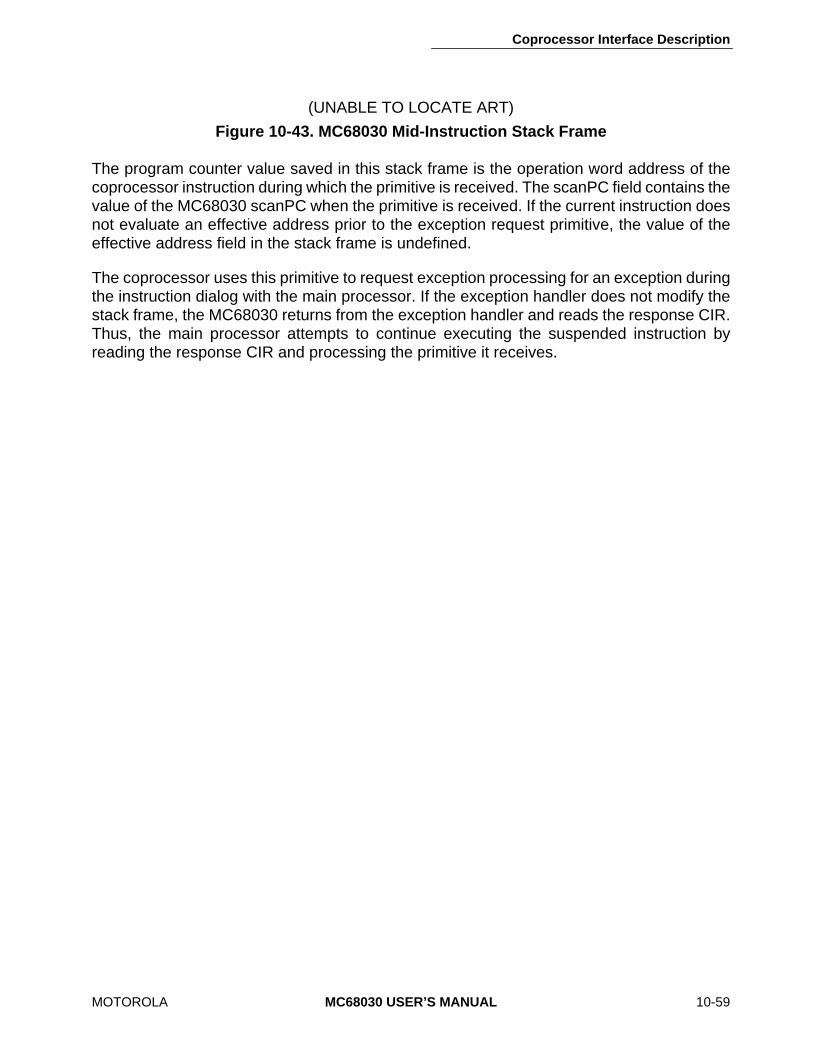
Coprocessor Interface Description
MOTOROLA MC68030 USER’S MANUAL 10-59
The program counter value saved in this stack frame is the operation word address of thecoprocessor instruction during which the primitive is received. The scanPC field contains thevalue of the MC68030 scanPC when the primitive is received. If the current instruction doesnot evaluate an effective address prior to the exception request primitive, the value of theeffective address field in the stack frame is undefined.
The coprocessor uses this primitive to request exception processing for an exception duringthe instruction dialog with the main processor. If the exception handler does not modify thestack frame, the MC68030 returns from the exception handler and reads the response CIR.Thus, the main processor attempts to continue executing the suspended instruction byreading the response CIR and processing the primitive it receives.
(UNABLE TO LOCATE ART)
Figure 10-43. MC68030 Mid-Instruction Stack Frame
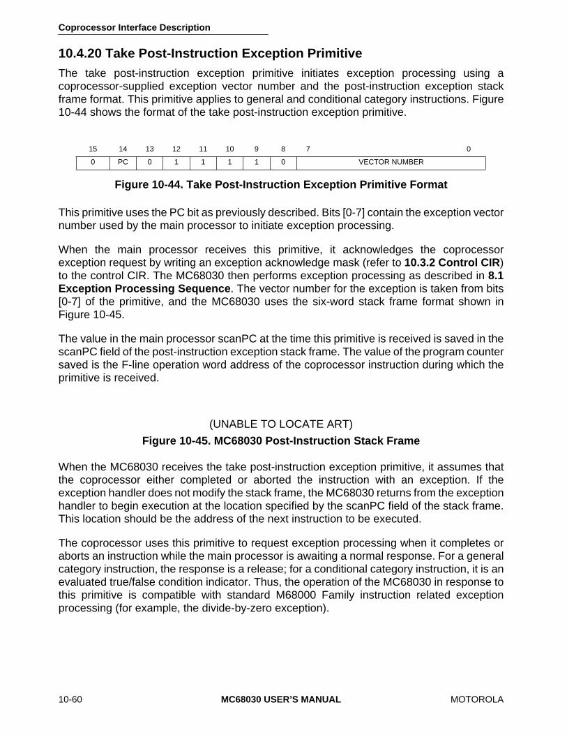
Coprocessor Interface Description
10-60 MC68030 USER’S MANUAL MOTOROLA
10.4.20 Take Post-Instruction Exception PrimitiveThe take post-instruction exception primitive initiates exception processing using acoprocessor-supplied exception vector number and the post-instruction exception stackframe format. This primitive applies to general and conditional category instructions. Figure10-44 shows the format of the take post-instruction exception primitive.
Figure 10-44. Take Post-Instruction Exception Primitive Format
This primitive uses the PC bit as previously described. Bits [0-7] contain the exception vectornumber used by the main processor to initiate exception processing.
When the main processor receives this primitive, it acknowledges the coprocessorexception request by writing an exception acknowledge mask (refer to 10.3.2 Control CIR)to the control CIR. The MC68030 then performs exception processing as described in 8.1Exception Processing Sequence. The vector number for the exception is taken from bits[0-7] of the primitive, and the MC68030 uses the six-word stack frame format shown inFigure 10-45.
The value in the main processor scanPC at the time this primitive is received is saved in thescanPC field of the post-instruction exception stack frame. The value of the program countersaved is the F-line operation word address of the coprocessor instruction during which theprimitive is received.
When the MC68030 receives the take post-instruction exception primitive, it assumes thatthe coprocessor either completed or aborted the instruction with an exception. If theexception handler does not modify the stack frame, the MC68030 returns from the exceptionhandler to begin execution at the location specified by the scanPC field of the stack frame.This location should be the address of the next instruction to be executed.
The coprocessor uses this primitive to request exception processing when it completes oraborts an instruction while the main processor is awaiting a normal response. For a generalcategory instruction, the response is a release; for a conditional category instruction, it is anevaluated true/false condition indicator. Thus, the operation of the MC68030 in response tothis primitive is compatible with standard M68000 Family instruction related exceptionprocessing (for example, the divide-by-zero exception).
15 14 13 12 11 10 9 8 7 0
0 PC 0 1 1 1 1 0 VECTOR NUMBER
(UNABLE TO LOCATE ART)
Figure 10-45. MC68030 Post-Instruction Stack Frame
Coprocessor Interface Description
MOTOROLA MC68030 USER’S MANUAL 10-61
10.5 EXCEPTIONSVarious exception conditions related to the execution of coprocessor instructions may occur.Whether an exception is detected by the main processor or by the coprocessor, the mainprocessor coordinates and performs exception processing. Servicing these coprocessor-related exceptions is an extension of the protocol used to service standard M68000 Familyexceptions. That is, when either the main processor detects an exception or is signaled bythe coprocessor that an exception condition has occurred, the main processor proceedswith exception processing as described in 8.1 Exception Processing Sequence.
10.5.1 Coprocessor-Detected ExceptionsExceptions that the coprocessor detects, also those that the main processor detects, areusually classified as coprocessor-detected exceptions. These exceptions can occur duringM68000 coprocessor interface operations, internal operations, or other system-relatedoperations of the coprocessor.
Most coprocessor-detected exceptions are signaled to the main processor through the useof one of the three take exception primitives defined for the M68000 coprocessor interface.The main processor responds to these primitives as previously described. However, not allcoprocessor-detected exceptions are signaled by response primitives. Coprocessor-detected format errors during the cpSAVE or cpRESTORE instruction are signaled to themain processor using the invalid format word described in 10.2.3.2.3 Invalid Format Word.
Coprocessor Interface Description
10-62 MC68030 USER’S MANUAL MOTOROLA
10.5.1.1 COPROCESSOR-DETECTED PROTOCOL VIOLATIONS. Protocol violationexceptions are communication failures between the main processor and coprocessoracross the M68000 coprocessor interface. Coprocessor-detected protocol violations occurwhen the main processor accesses entries in the coprocessor interface register set in anunexpected sequence. The sequence of operations that the main processor performs for agiven coprocessor instruction or coprocessor response primitive has been describedpreviously in this section.
A coprocessor can detect protocol violations in various ways. According to the M68000coprocessor interface protocol, the main processor always accesses the operation word,operand, register select, instruction address, or operand address CIRs synchronously withrespect to the operation of the coprocessor. That is, the main processor accesses these fiveregisters in a certain sequence, and the coprocessor expects them to be accessed in thatsequence. As a minimum, all M68000 coprocessors should detect a protocol violation if themain processor accesses any of these five registers when the coprocessor is expecting anaccess to either the command or condition CIR. Likewise, if the coprocessor is expectingan access to the command or condition CIR and the main processor accesses one of thesefive registers, the coprocessor should detect and signal a protocol violation.
According to the M68000 coprocessor interface protocol, the main processor can perform aread of either the save or response CIRs or a write of either the restore or control CIRsasynchronously with respect to the operation of the coprocessor. That is, an access to oneof these registers without the coprocessor explicitly expecting that access at that point canbe a valid access. Although the coprocessor can anticipate certain accesses to the restore,response, and control coprocessor interface registers, these registers can be accessed atother times also.
The coprocessor cannot signal a protocol violation to the main processor during theexecution of cpSAVE or cpRESTORE instructions. If a coprocessor detects a protocolviolation during the cpSAVE or cpRESTORE instruction, it should signal the exception to themain processor when the next coprocessor instruction is initiated.
The main philosophy of the coprocessor-detected protocol violation is that the coprocessorshould always acknowledge an access to one of its interface registers. If the coprocessordetermines that the access is not valid, it should assert DSACKx, to the main processor andsignal a protocol violation when the main processor next reads the response CIR. If thecoprocessor fails to assert DSACKx, the main processor waits for the assertion of that signal(or some other bus termination signal) indefinitely. The protocol previously describedensures that the coprocessor cannot halt the main processor.
Coprocessor Interface Description
MOTOROLA MC68030 USER’S MANUAL 10-63
The coprocessor can signal a protocol violation to the main processor with the take mid-instruction exception primitive. To maintain consistency, the vector number should be 13, asit is for a protocol violation detected by the main processor. When the main processor readsthis primitive, it proceeds as described in 10.4.19 Take Mid-Instruction ExceptionPrimitive. If the exception handler does not modify the stack frame, the MC68030 returnsfrom the exception handler and reads the response CIR.
10.5.1.2 COPROCESSOR-DETECTED ILLEGAL COMMAND OR CONDITION WORDS. Illegal coprocessor command or condition words are values written to the command CIR orcondition CIR that the coprocessor does not recognize. If a value written to either of theseregisters is not valid, the coprocessor should return the take pre-instruction exceptionprimitive in the response CIR. When it receives this primitive, the main processor takes apre-instruction exception as described in 10.4.18 Take Pre-Instruction ExceptionPrimitive. If the exception handler does not modify the main processor stack frame, an RTEinstruction causes the MC68030 to reinitiate the instruction that took the exception. Thecoprocessor designer should ensure that the state of the coprocessor is not irrecoverablyaltered by an illegal command or condition exception if the system supports emulation of theunrecognized command or condition word.
All Motorola M68000 coprocessors signal illegal command and condition words by returningthe take pre-instruction exception primitive with the F-line emulator exception vector number11.
10.5.1.3 COPROCESSOR DATA-PROCESSING EXCEPTIONS. Exceptions related to theinternal operation of a coprocessor are classified as data-processing-related exceptions.These exceptions are analogous to the divide-by-zero exception defined by M68000microprocessors and should be signaled to the main processor using one of the three takeexception primitives containing an appropriate exception vector number. Which of thesethree primitives is used to signal the exception is usually determined by the point in theinstruction operation where the main processor should continue the program flow afterexception processing. Refer to 110.4.18 Take Pre-Instruction Exception Primitive,10.4.19 Take Mid-Instruction Exception Primitive, and 10.4.20 Take Post-InstructionException Primitive.
Coprocessor Interface Description
10-64 MC68030 USER’S MANUAL MOTOROLA
10.5.1.4 COPROCESSOR SYSTEM-RELATED EXCEPTIONS. System-relatedexceptions detected by a DMA coprocessor include those associated with bus activity andany other exceptions (interrupts, for example) occurring external to the coprocessor. Theactions taken by the coprocessor and the main processor depend on the type of exceptionthat occurs.
When an address or bus error is detected by a DMA coprocessor, the coprocessor shouldstore any information necessary for the main processor exception handling routines insystem-accessible registers. The coprocessor should place one of the three take exceptionprimitives encoded with an appropriate exception vector number in the response CIR. Whichof the three primitives is used depends upon the point in the coprocessor instruction at whichthe exception was detected and the point in the instruction execution at which the mainprocessor should continue after exception processing.
10.5.1.5 FORMAT ERRORS. Format errors are the only coprocessor-detected exceptionsthat are not signaled to the main processor with a response primitive. When the mainprocessor writes a format word to the restore CIR during the execution of a cpRESTOREinstruction, the coprocessor decodes this word to determine if it is valid (refer to 10.2.3.3Coprocessor Context Save Instruction). If the format word is not valid, the coprocessorplaces the invalid format code in the restore CIR. When the main processor reads the invalidformat code, it aborts the coprocessor instruction by writing an abort mask (refer to 10.3.2Control CIR) to the control CIR. The main processor then performs exception processingusing a four-word pre-instruction stack frame and the format error exception vector number14. Thus, if the exception handler does not modify the stack frame, the MC68030 restartsthe cpRESTORE instruction when the RTE instruction in the handler is executed. If thecoprocessor returns the invalid format code when the main processor reads the save CIRto initiate a cpSAVE instruction, the main processor performs format error exceptionprocessing as outlined for the cpRESTORE instruction.
Coprocessor Interface Description
MOTOROLA MC68030 USER’S MANUAL 10-65
10.5.2 Main-Processor-Detected ExceptionsA number of exceptions related to coprocessor instruction execution are detected by themain processor instead of the coprocessor (they are still serviced by the main processor).These exceptions can be related to the execution of coprocessor response primitives,communication across the M68000 coprocessor interface, or the completion of conditionalcoprocessor instructions by the main processor.
10.5.2.1 PROTOCOL VIOLATIONS . The main processor detects a protocol violation whenit reads a primitive from the response CIR that is not a valid primitive. The protocol violationsthat can occur in response to the primitives defined for the M68000 coprocessor interfaceare summarized in Table 10-6.
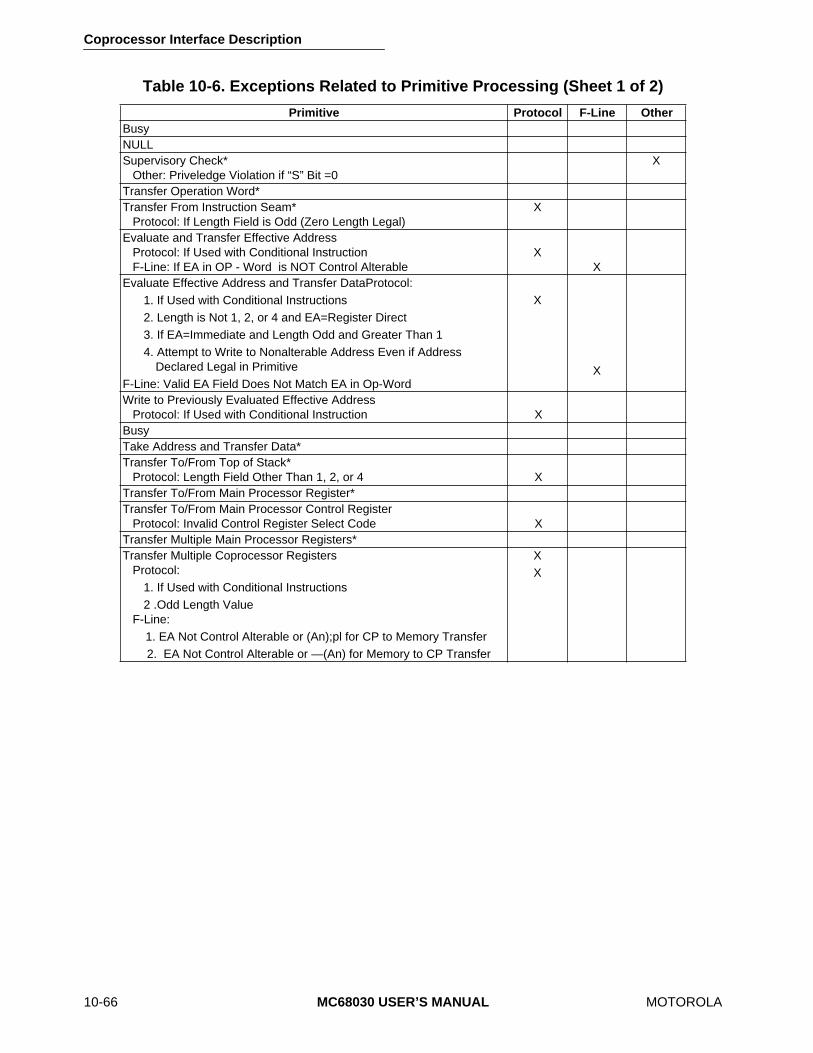
Coprocessor Interface Description
10-66 MC68030 USER’S MANUAL MOTOROLA
Table 10-6. Exceptions Related to Primitive Processing (Sheet 1 of 2)
Primitive Protocol F-Line OtherBusyNULLSupervisory Check*
Other: Priveledge Violation if “S” Bit =0X
Transfer Operation Word*Transfer From Instruction Seam*
Protocol: If Length Field is Odd (Zero Length Legal)X
Evaluate and Transfer Effective AddressProtocol: If Used with Conditional InstructionF-Line: If EA in OP - Word is NOT Control Alterable
XX
Evaluate Effective Address and Transfer DataProtocol:1. If Used with Conditional Instructions2. Length is Not 1, 2, or 4 and EA=Register Direct3. If EA=Immediate and Length Odd and Greater Than 14. Attempt to Write to Nonalterable Address Even if Address
Declared Legal in PrimitiveF-Line: Valid EA Field Does Not Match EA in Op-Word
X
X
Write to Previously Evaluated Effective AddressProtocol: If Used with Conditional Instruction X
BusyTake Address and Transfer Data*Transfer To/From Top of Stack*
Protocol: Length Field Other Than 1, 2, or 4 XTransfer To/From Main Processor Register*Transfer To/From Main Processor Control Register
Protocol: Invalid Control Register Select Code XTransfer Multiple Main Processor Registers*Transfer Multiple Coprocessor Registers
Protocol:1. If Used with Conditional Instructions2 .Odd Length Value
F-Line:1. EA Not Control Alterable or (An);pl for CP to Memory Transfer 2. EA Not Control Alterable or —(An) for Memory to CP Transfer
XX

Coprocessor Interface Description
MOTOROLA MC68030 USER’S MANUAL 10-67
*Use of this primitive with CA=0 will cause protocol violation on conditional instructions.Abbreviations: EA=Effective Address CP=Coprocessor
When the MC68030 detects a protocol violation, it does not automatically notify thecoprocessor of the resulting exception by writing to the control CIR. The exception handlingroutine may, however, use the MOVES instruction to read the response CIR and thusdetermine the primitive that caused the MC68030 to initiate protocol violation exceptionprocessing. The main processor initiates exception processing using the mid-instructionstack frame (refer to Figure 10-43) and the coprocessor protocol violation exception vectornumber 13. If the exception handler does not modify the stack frame, the main processorreads the response CIR again following the execution of an RTE instruction to return fromthe exception handler. This protocol allows extensions to the M68000 coprocessor interfaceto be emulated in software by a main processor that does not provide hardware support forthese extensions. Thus, the protocol violation is transparent to the coprocessor if theprimitive execution can be emulated in software by the main processor.
Primitive Protocol F-Line OtherTransfer Status and/or ScanPC
Protocol: If Used with Conditional InstructionOther:
1. Trace — Trace Made Pending if MC68020 in ``Trace on Change of Flow'' Mode and DR=1
2. Address Error — If Odd value Written to ScanPC
X
X
Take Pre-Instruction, Mid-Instruction, or Post-Instruction ExceptionException Depends on Vector Supplies in Primitive
X X X
Coprocessor Interface Description
10-68 MC68030 USER’S MANUAL MOTOROLA
10.5.2.2 F-LINE EMULATOR EXCEPTIONS. The F-line emulator exceptions detected bythe MC68030 are either explicitly or implicitly related to the encodings of F-line operationwords in the instruction stream. If the main processor determines that an F-line operationword is not valid, it initiates F-line emulator exception processing. Any F-line operation wordwith bits [8:6]=110 or 111 causes the MC68030 to initiate exception processing withoutinitiating any communication with the coprocessor for that instruction. Also, an operationword with bits [8:6]=000-101 that does not map to one of the valid coprocessor instructionsin the instruction set causes the MC68030 to initiate F-line emulator exception processing.If the F-line emulator exception is either of these two situations, the main processor doesnot write to the control CIR prior to initiating exception processing.
F-line exceptions can also occur if the operations requested by a coprocessor responseprimitive are not compatible with the effective address type in bits [0-5] of the coprocessorinstruction operation word. The F-line emulator exceptions that can result from the use ofthe M68000 coprocessor response primitives are summarized in Table 10-6. If the exceptionis caused by receiving an invalid primitive, the main processor aborts the coprocessorinstruction in progress by writing an abort mask (refer to 10.3.2 Control CIR) to the controlCIR prior to F-line emulator exception processing.
Another type of F-line emulator exception occurs when a bus error occurs during thecoprocessor interface register access that initiates a coprocessor instruction. The mainprocessor assumes that the coprocessor is not present and takes the exception.
When the main processor initiates F-line emulator exception processing, it uses the four-word pre-instruction exception stack frame (refer to Figure 10-41) and the F-line emulatorexception vector number 11. Thus, if the exception handler does not modify the stack frame,the main processor attempts to restart the instruction that caused the exception after itexecutes an RTE instruction to return from the exception handler.
If the cause of the F-line exception can be emulated in software, the handler stores theresults of the emulation in the appropriate registers of the programmer's model and in thestatus register field of the saved stack frame. The exception handler adjusts the programcounter field of the saved stack frame to point to the next instruction operation word andexecutes the RTE instruction. The MC68030 then executes the instruction following theinstruction that was emulated.
Coprocessor Interface Description
MOTOROLA MC68030 USER’S MANUAL 10-69
The exception handler should also check the copy of the status register on the stack todetermine whether tracing is on. If tracing is on, the trace exception processing should alsobe emulated. Refer to 8.1.7 Trace Exception.
10.5.2.3 PRIVILEGE VIOLATIONS. Privilege violations can result from the cpSAVE andcpRESTORE instructions and, also, from the supervisor check coprocessor responseprimitive. The main processor initiates privilege violation exception processing if it attemptsto execute either the cpSAVE or cpRESTORE instruction when it is in the user state (S=0in status register). The main processor initiates this exception processing prior to anycommunication with the coprocessor associated with the cpSAVE or cpRESTOREinstructions.
If the main processor is executing a coprocessor instruction in the user state when it readsthe supervisor check primitive, it aborts the coprocessor instruction in progress by writing anabort mask (refer to 10.3.2 Control CIR) to the control CIR. The main processor thenperforms privilege violation exception processing.
If a privilege violation occurs, the main processor initiates exception processing using thefour-word pre-instruction stack frame (refer to Figure 10-41) and the privilege violationexception vector number 8. Thus, if the exception handler does not modify the stack frame,the main processor attempts to restart the instruction during which the exception occurredafter it executes an RTE to return from the handler.
10.5.2.4 CPTRAPCC INSTRUCTION TRAPS. If, during the execution of a cpTRAPccinstruction, the coprocessor returns the TRUE condition indicator to the main processor witha null primitive, the main processor initiates trap exception processing. The main processoruses the six-word post-instruction exception stack frame (refer to Figure 10-45) and the trapexception vector number 7. The scanPC field of this stack frame contains the address of theinstruction following the cpTRAPcc instruction. The processing associated with thecpTRAPcc instruction can then proceed, and the exception handler can locate anyimmediate operand words encoded in the cpTRAPcc instruction using the informationcontained in the six-word stack frame. If the exception handler does not modify the stackframe, the main processor executes the instruction following the cpTRAPcc instruction afterit executes an RTE instruction to exit from the handler.
Coprocessor Interface Description
10-70 MC68030 USER’S MANUAL MOTOROLA
10.5.2.5 TRACE EXCEPTIONS. The MC68030 supports two modes of instruction tracing,discussed in 8.1.7 Trace Exception. In the trace on instruction execution mode, theMC68030 takes a trace exception after completing each instruction. In the trace on changeof flow mode, the MC68030 takes a trace exception after each instruction that alters thestatus register or places an address other than the address of the next instruction in programcounter.
The protocol used to execute coprocessor cpSAVE, cpRESTORE, or conditional categoryinstructions does not change when a trace exception is pending in the main processor. Themain processor performs a pending trace on instruction execution exception aftercompleting the execution of that instruction. If the main processor is in the trace on changeof flow mode and an instruction places an address other than that of the next instruction inthe program counter, the processor takes a trace exception after it executes the instruction.
If a trace exception is not pending during a general category instruction, the main processorterminates communication with the coprocessor after reading any primitive with CA=0.Thus, the coprocessor can complete a cpGEN instruction concurrently with the execution ofinstructions by the main processor. When a trace exception is pending, however, the mainprocessor must ensure that all processing associated with a cpGEN instruction has beencompleted before it takes the trace exception. In this case, the main processor continues toread the response CIR and to service the primitives until it receives either a null, CA=0,PF=1 primitive, or until exception processing caused by a take post-instruction exceptionprimitive has completed. The coprocessor should return the null, CA=0 primitive with PF=0,while it is completing the execution of the cpGEN instruction. The main processor mayservice pending interrupts between reads of the response CIR if IA=1 in these primitives(refer to Table 10-3). This protocol ensures that a trace exception is not taken until allprocessing associated with a cpGEN instruction has completed.
If T1:T0=01 in the MC68030 status register (trace on change of flow) when a generalcategory instruction is initiated, a trace exception is taken for the instruction only when thecoprocessor issues a transfer status register and scanPC primitive with DR=1 during theexecution of that instruction. In this case, it is possible that the coprocessor is still executingthe cpGEN instruction concurrently when the main processor begins execution of the traceexception handler. A cpSAVE instruction executed during the trace on change of flowexception handler could thus suspend the execution of a concurrently operating cpGENinstruction.
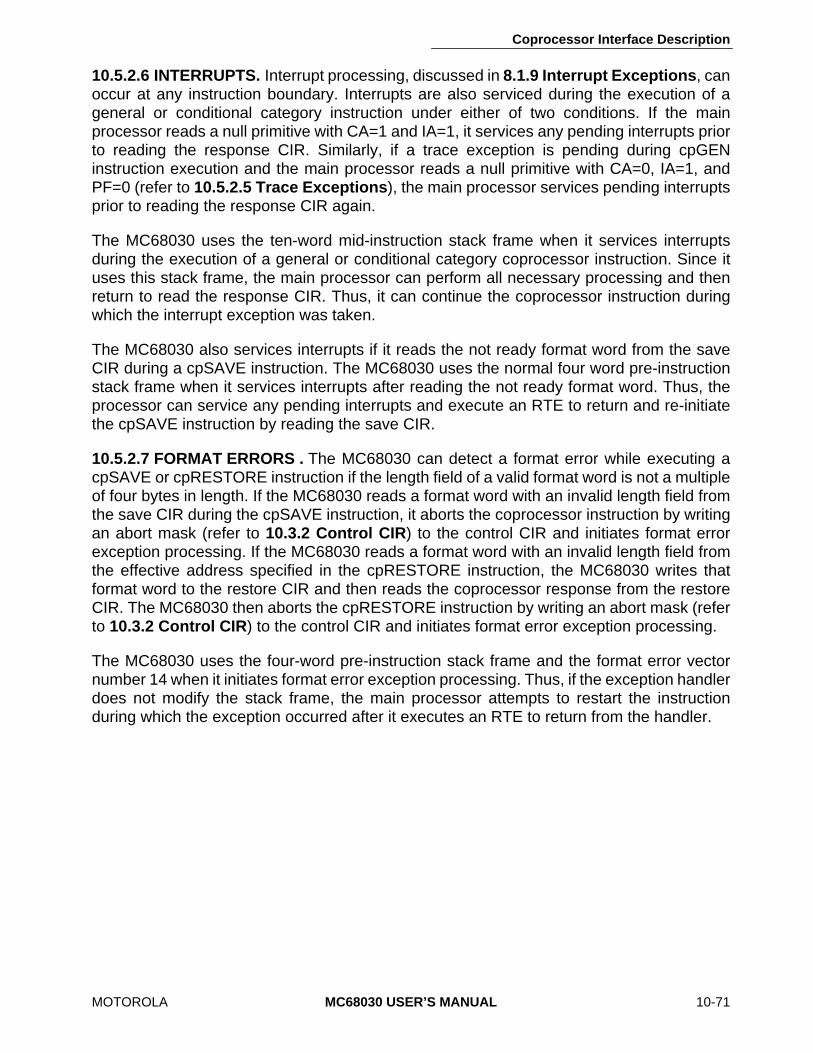
Coprocessor Interface Description
MOTOROLA MC68030 USER’S MANUAL 10-71
10.5.2.6 INTERRUPTS. Interrupt processing, discussed in 8.1.9 Interrupt Exceptions, canoccur at any instruction boundary. Interrupts are also serviced during the execution of ageneral or conditional category instruction under either of two conditions. If the mainprocessor reads a null primitive with CA=1 and IA=1, it services any pending interrupts priorto reading the response CIR. Similarly, if a trace exception is pending during cpGENinstruction execution and the main processor reads a null primitive with CA=0, IA=1, andPF=0 (refer to 10.5.2.5 Trace Exceptions), the main processor services pending interruptsprior to reading the response CIR again.
The MC68030 uses the ten-word mid-instruction stack frame when it services interruptsduring the execution of a general or conditional category coprocessor instruction. Since ituses this stack frame, the main processor can perform all necessary processing and thenreturn to read the response CIR. Thus, it can continue the coprocessor instruction duringwhich the interrupt exception was taken.
The MC68030 also services interrupts if it reads the not ready format word from the saveCIR during a cpSAVE instruction. The MC68030 uses the normal four word pre-instructionstack frame when it services interrupts after reading the not ready format word. Thus, theprocessor can service any pending interrupts and execute an RTE to return and re-initiatethe cpSAVE instruction by reading the save CIR.
10.5.2.7 FORMAT ERRORS . The MC68030 can detect a format error while executing acpSAVE or cpRESTORE instruction if the length field of a valid format word is not a multipleof four bytes in length. If the MC68030 reads a format word with an invalid length field fromthe save CIR during the cpSAVE instruction, it aborts the coprocessor instruction by writingan abort mask (refer to 10.3.2 Control CIR) to the control CIR and initiates format errorexception processing. If the MC68030 reads a format word with an invalid length field fromthe effective address specified in the cpRESTORE instruction, the MC68030 writes thatformat word to the restore CIR and then reads the coprocessor response from the restoreCIR. The MC68030 then aborts the cpRESTORE instruction by writing an abort mask (referto 10.3.2 Control CIR) to the control CIR and initiates format error exception processing.
The MC68030 uses the four-word pre-instruction stack frame and the format error vectornumber 14 when it initiates format error exception processing. Thus, if the exception handlerdoes not modify the stack frame, the main processor attempts to restart the instructionduring which the exception occurred after it executes an RTE to return from the handler.

Coprocessor Interface Description
10-72 MC68030 USER’S MANUAL MOTOROLA
10.5.2.8 ADDRESS AND BUS ERRORS. Coprocessor-instruction-related bus faults canoccur during main processor bus cycles to CPU space to communicate with a coprocessoror during memory cycles run as part of the coprocessor instruction execution. If a bus erroroccurs during the coprocessor interface register access that is used to initiate a coprocessorinstruction, the main processor assumes that the coprocessor is not present and takes anF-line emulator exception as described in 10.5.2.2 F-Line Emulator Exceptions. That is,the processor takes an F-line emulator exception when a bus error occurs during the initialaccess to a CIR by a coprocessor instruction. If a bus error occurs on any other coprocessoraccess or on a memory access made during the execution of a coprocessor instruction, themain processor performs bus error exception processing as described in 8.1.2 Bus ErrorException. After the exception handler has corrected the cause of the bus error, the mainprocessor can return to the point in the coprocessor instruction at which the fault occurred.
An address error occurs if the MC68030 attempts to prefetch an instruction from an oddaddress. This can occur if the calculated destination address of a cpBcc or cpDBccinstruction is odd or if an odd value is transferred to the scanPC with the transfer statusregister and the scanPC response primitive. If an address error occurs, the MC68030performs exception processing for a bus fault as described in 8.1.3 Address ErrorException.
10.5.3 Coprocessor ResetEither an external reset signal or a RESET instruction can reset the external devices of asystem. The system designer can design a coprocessor to be reset and initialized by bothreset types or by external reset signals only. To be consistent with the MC68030 design, thecoprocessor should be affected by external reset signals only and not by RESETinstructions, because the coprocessor is an extension to the main processor programmingmodel and to the internal state of the MC68030.
10.6 COPROCESSOR SUMMARYCoprocessor instruction formats are presented for reference. Refer to the M68000PM/AD,M68000 Programmer's Reference Manual, for detailed information on coprocessorinstructions.
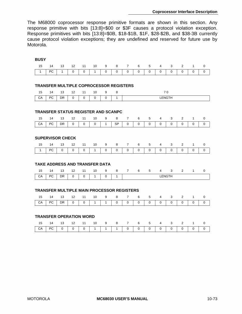
Coprocessor Interface Description
MOTOROLA MC68030 USER’S MANUAL 10-73
The M68000 coprocessor response primitive formats are shown in this section. Anyresponse primitive with bits [13:8]=$00 or $3F causes a protocol violation exception.Response primitives with bits [13:8]=$0B, $18-$1B, $1F, $28-$2B, and $38-3B currentlycause protocol violation exceptions; they are undefined and reserved for future use byMotorola.
BUSY
15 14 13 12 11 10 9 8 7 6 5 4 3 2 1 0
1 PC 1 0 0 1 0 0 0 0 0 0 0 0 0 0
TRANSFER MULTIPLE COPROCESSOR REGISTERS
15 14 13 12 11 10 9 8 7 0
CA PC DR 0 0 0 0 1 LENGTH
TRANSFER STATUS REGISTER AND SCANPC
15 14 13 12 11 10 9 8 7 6 5 4 3 2 1 0
CA PC DR 0 0 0 1 SP 0 0 0 0 0 0 0 0
SUPERVISOR CHECK
15 14 13 12 11 10 9 8 7 6 5 4 3 2 1 0
1 PC 0 0 0 1 0 0 0 0 0 0 0 0 0 0
TAKE ADDRESS AND TRANSFER DATA
15 14 13 12 11 10 9 8 7 6 5 4 3 2 1 0
CA PC DR 0 0 1 0 1 LENGTH
TRANSFER MULTIPLE MAIN PROCESSOR REGISTERS
15 14 13 12 11 10 9 8 7 6 5 4 3 2 1 0
CA PC DR 0 0 1 1 0 0 0 0 0 0 0 0 0
TRANSFER OPERATION WORD
15 14 13 12 11 10 9 8 7 6 5 4 3 2 1 0
CA PC 0 0 0 1 1 1 0 0 0 0 0 0 0 0
Coprocessor Interface Description
10-74 MC68030 USER’S MANUAL MOTOROLA
NULL
15 14 13 12 11 10 9 8 7 6 5 4 3 2 1 0
CA PC 0 0 1 0 0 IA 0 0 0 0 0 0 PF TF
EVALUATE AND TRANSFER EFFECTIVE ADDRESS
15 14 13 12 11 10 9 8 7 6 5 4 3 2 1 0
CA PC 0 0 1 0 1 0 0 0 0 0 0 0 0 0
TRANSFER SINGLE MAIN PROCESSOR REGISTER
15 14 13 12 11 10 9 8 7 6 5 4 3 2 0
CA PC DR 0 1 1 0 0 0 0 0 0 D/A REGISTER
TRANSFER MAIN PROCESSOR CONTROL REGISTER
15 14 13 12 11 10 9 8 7 6 5 4 3 2 1 0
CA PC DR 0 1 1 0 1 0 0 0 0 0 0 0 0
TRANSFER TO/FROM TOP OF STACK
15 14 13 12 11 10 9 8 7 0
CA PC DR 0 1 1 1 0 LENGTH
TRANSFER FROM INSTRUCTION STREAM
15 14 13 12 11 10 9 8 7 0
CA PC 0 0 1 1 1 1 LENGTH
EVALUATE EFFECTIVE ADDRESS AND TRANSFER DATA
15 14 13 12 11 10 9 8 7 0
CA PC DR 1 0 VALID EA LENGTH
TAKE PRE-INSTRUCTION EXCEPTION
15 14 13 12 11 10 9 8 7 0
0 PC 0 1 1 1 0 0 VECTOR NUMBER

Coprocessor Interface Description
10-75 MC68030 USER’S MANUAL MOTOROLA
TAKE MID-INSTRUCTION EXCEPTION
15 14 13 12 11 10 9 8 7 0
0 PC 0 1 1 1 0 1 VECTOR NUMBER
TAKE POST-INSTRUCTION EXCEPTION
15 14 13 12 11 10 9 8 7 0
0 PC 0 1 1 1 1 0 VECTOR NUMBER
WRITE TO PREVIOUSLY EVALUATED EFFECTIVE ADDRESS
15 14 13 12 11 10 9 8 7 0
CA PC 1 0 0 0 0 0 LENGTH
MOTOROLA
MC68030 USER’S MANUAL
11-1
SECTION 11INSTRUCTION EXECUTION TIMING
This section describes the instruction execution and operations (table searches, etc.) of theMC68030 in terms of external clock cycles. It provides accurate execution and operationtiming guidelines but not exact timings for every possible circumstance. This approach isused since exact execution time for an instruction or operation is highly dependent onmemory speeds and other variables. The timing numbers presented in this section allow theassembly language programmer or compiler writer to predict actual cache-case andaverage no-cache-case timings needed to evaluate the performance of the MC68030.Additionally, the timings for exception processing, context switching, and interruptprocessing are included so that designers of multi-tasking or real-time systems can predicttask switch overhead, maximum interrupt latency, and similar timing parameters.
In this section, instruction and operation times are shown in clock cycles to eliminate clockfrequency dependencies.
11.1 PERFORMANCE TRADEOFFS
The MC68030 maximizes average performance at the expense of worst case performance.The time spent executing one instruction can vary from zero to over 100 clocks. Factorsaffecting the execution time are the preceding and following instructions, the instructionstream alignment, residency of operands and instruction words in the caches, residency ofaddress translations in the address translation cache, and operand alignment.
To increase the average performance of the MC68030, certain tradeoffs were made toincrease best case performance and to decrease the occurrence of worst case behavior. Forexample, burst filling increases performance by prefetching data for later accesses, but itcommits the external bus controller and a cache for a longer period.
The MC68030 can overlap data writes with instruction cache reads, data cache reads, and/or microsequencer execution. Instruction cache reads can be overlapped with data cachefills and/or microsequencer activity. Similarly, data cache reads can be overlapped withinstruction cache fills and/or microsequencer activity. The execution of an instruction thatonly accesses on-chip registers can be overlapped entirely with a concurrent data writegenerated by a previous instruction, if prefetches generated by that instruction are residentin the instruction cache.

Instruction Execution Timing
11-2
MC68030 USER’S MANUAL
MOTOROLA
11.2 RESOURCE SCHEDULING
Some of the variability in instruction execution timings results from the overlap of resourceutilization. The processor can be viewed as consisting of eight independently scheduledresources. Since very little of the scheduling is directly related to instruction boundaries, itis impossible to make accurate estimates of the time required to execute a particularinstruction without knowing the complete context within which the instruction is executing.The position of these resources within the MC68030 is shown in Figure 11-1.
11.2.1 Microsequencer
The microsequencer is either executing microinstructions or awaiting completion ofaccesses that are necessary to continue executing microcode. The bus controller isresponsible for all bus activity. The microsequencer controls the bus controller, instructionexecution, and internal processor operations such as calculation of effective addresses andsetting of condition codes. The microsequencer initiates instruction word prefetches andcontrols the validation of instruction words in the instruction pipe.
11.2.2 Instruction Pipe
The MC68030 contains a three-word instruction pipe where instruction opcodes aredecoded. As shown in Figure 11-1, instruction words (instruction operation words and allextension words) enter the pipe at stage B and proceed to stages C and D. An instructionword is completely decoded when it reaches stage D of the pipe. Each of the pipe stageshas a status bit that reflects whether the word in the stage was loaded with data from a buscycle that was terminated abnormally. Stages of the pipe are only filled in response tospecific prefetch requests issued by the microsequencer.
Words are loaded into the instruction pipe from the cache holding register. While theindividual stages of the pipe are only 16 bits wide, the cache holding register is 32 bits wideand contains the entire long word. This long word is obtained from the instruction cache orthe external bus in response to a prefetch request from the microsequencer. When themicrosequencer requests an even-word (long-word aligned) prefetch, the entire long wordis accessed from the instruction cache or the external bus and loaded into the cache holdingregister, and the high-order word is also loaded into stage B of the pipe. The instruction wordfor the next sequential prefetch can then be accessed directly from the cache holdingregister, and no external bus cycle or instruction cache access is required. The cacheholding register provides instruction words to the pipe, regardless of whether the instructioncache is enabled or disabled.
Instruction Execution Timing
MOTOROLA
MC68030 USER’S MANUAL
11-3
Prefetch requests are simultaneously submitted to the cache holding register, the instructioncache, and the bus controller. Thus, even if the instruction cache is disabled, an instructionprefetch may hit in the cache holding register and cause an external bus cycle to be aborted.
11.2.3 Instruction Cache
The instruction cache services the instruction prefetch portion of the microsequencer. Theprefetch of an instruction that hits in the on-chip instruction cache causes no delay ininstruction execution since no external bus activity is required for the prefetch. Theinstruction cache also interacts with the external bus during instruction cache fills followinginstruction cache misses.
11.2.4 Data Cache
The data cache services data reads and is updated on data writes. Data operands requiredby the execution unit that are accessed from the data cache cause no delay in instructionexecution due to external bus activity for the data fetch. The data cache also interacts withthe external bus during data cache fills following data cache misses.
11.2.5 Bus Controller Resources
Prefetches that miss in the instruction cache cause an external memory cycle to beperformed. Similarly, when data reads miss in the on-chip data cache, an external memorycycle is required. The time required for either of these bus cycles may be overlapped withother internal activity.
The bus controller and microsequencer can operate on an instruction concurrently. The buscontroller can perform a read or write while the microsequencer controls an effectiveaddress calculation or sets the condition codes. The microsequencer may also request abus cycle that the bus controller cannot perform immediately. In this case, the bus cycle isqueued and the bus controller runs the cycle when the current cycle is complete.
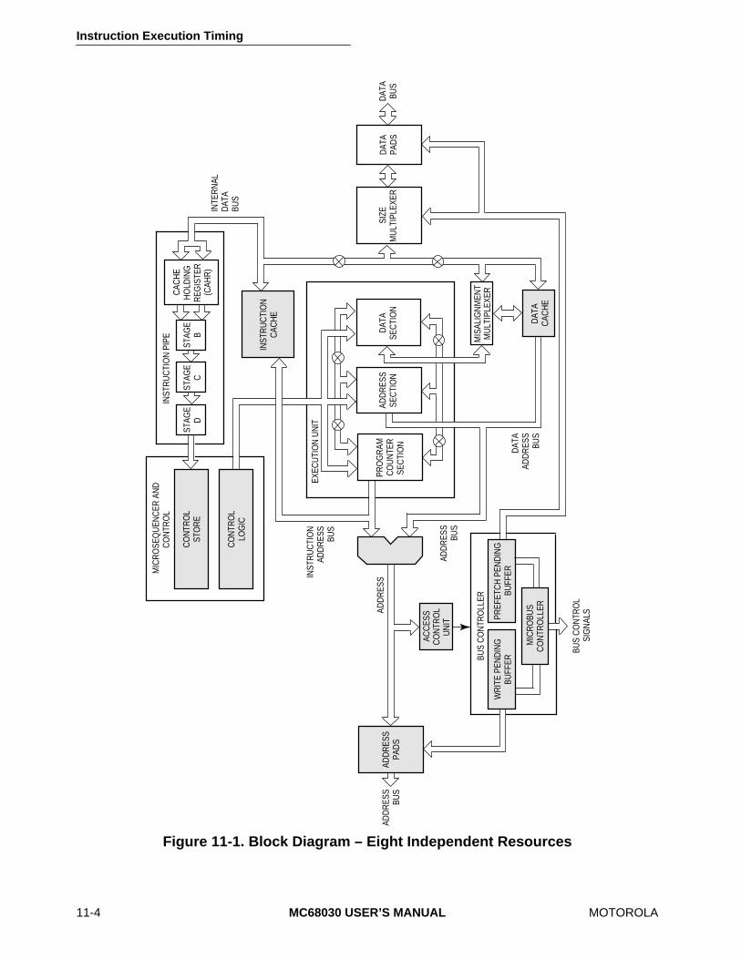
Instruction Execution Timing
11-4
MC68030 USER’S MANUAL
MOTOROLA
Figure 11-1. Block Diagram – Eight Independent Resources
MIC
RO
SEQ
UEN
CER
AN
DC
ON
TRO
L
CO
NTR
OL
STO
RE
INST
RU
CTI
ON
CAC
HE
STAG
EB
STAG
EC
STAG
ED
INTE
RN
ALD
ATA
BUS
INST
RU
CTI
ON
PIP
E
INST
RU
CTI
ON
ADD
RES
SBU
S
ADD
RES
SSE
CTI
ON
PRO
GR
AMC
OU
NTE
RSE
CTI
ON
DAT
ASE
CTI
ON
EXEC
UTI
ON
UN
IT
MIS
ALIG
NM
ENT
MU
LTIP
LEXE
R
SIZE
MU
LTIP
LEXE
RD
ATA
PAD
SD
ATA
BUS
WR
ITE
PEN
DIN
GBU
FFER
PREF
ETC
H P
END
ING
BUFF
ER
MIC
RO
BUS
CO
NTR
OLL
ER
BUS
CO
NTR
OLL
ER
BUS
CO
NTR
OL
SIG
NAL
S
ADD
RES
SBU
S
ADD
RES
SPA
DS
ADD
RES
SBU
S
ADD
RES
S
DAT
AC
ACH
E
DAT
AAD
DR
ESS
BUS
CAC
HE
HO
LDIN
GR
EGIS
TER
(CAH
R)
ACC
ESS
CO
NTR
OL
UN
IT
CO
NTR
OL
LOG
IC
Instruction Execution Timing
MOTOROLA
MC68030 USER’S MANUAL
11-5
The bus controller consists of the micro bus controller, the instruction fetch pending buffer,and the write pending buffer. These three resources carry out all writes and reads that missin the on-chip caches.
11.2.5.1 INSTRUCTION FETCH PENDING BUFFER.
The instruction prefetch mechanismincludes a single long-word instruction fetch pending buffer. Interlocks are provided toprevent this buffer from being overwritten by an instruction prefetch request before apreviously requested prefetch is completed.
11.2.5.2 WRITE PENDING BUFFER.
The MC68030 incorporates a single write pendingbuffer, allowing the microsequencer to continue execution after the request for a write cycleproceeds to the bus controller. Interlocks prevent the microsequencer from overwriting thisbuffer.
11.2.5.3 MICRO BUS CONTROLLER.
The micro bus controller performs the bus cyclesissued to the bus controller by the rest of the processor. It implements any dynamic bussizing required and also controls burst operations.
When prefetching instructions from external memory, the micro bus controller utilizes long-word read cycles. The processor reads two words, which may load two instructions at onceor two words of a multi-word instruction into the cache holding register (and the instructioncache if it is enabled and not frozen). A special case occurs when prefetch, that correspondsto an instruction word at an odd-word boundary, is not found in the cache holding register(e.g., due to a branch to an odd-word location) with an instruction cache miss. From a 32-bit memory, the MC68030 reads both the even and odd words associated with the long-wordbase address in one bus cycle. From an 8- or 16-bit memory, the processor reads the evenword before the odd word. Both the even and odd word are loaded into the cache holdingregister (and the instruction cache if it is enabled and not frozen).

Instruction Execution Timing
11-6
MC68030 USER’S MANUAL
MOTOROLA
11.2.6 Memory Management Unit
The MC68030 includes a memory management unit (MMU) that translates logicaladdresses to physical addresses for external accesses when required. The MMU uses anaddress translation cache (ATC) to store recently used translations. When the physicaladdress corresponding to a logical address resides in the ATC, the address translation timeis completely overlapped with on-chip cache accesses and has no effect on instructiontiming.
When the ATC does not contain the translation for a logical address, the processor performsa table search operation to external memory. The amount of time required for a table searchdepends on the structure of the address translation tree and whether a nonresident portionof the translation tree is required.
The MMU supports demand-paged virtual memory. When a table search terminates with anexception, indicating that the requested instruction or data is not resident, additional time tobring the appropriate page into memory is required. The time required is dependent on thehandling routine for the exception.
11.3 INSTRUCTION EXECUTION TIMING CALCULATIONS
The instruction-cache-case timing, overlap, average no-cache-case timing, and actualinstruction-cache-case execution time calculations are discussed in the followingparagraphs.
11.3.1 Instruction-Cache Case
The instruction-cache-case (CC) time for an instruction is the total number of clock periodsrequired to execute the instruction, provided all the corresponding instruction prefetches areresident in the on-chip instruction cache. All bus cycles are assumed to take two clockperiods. The instruction-cache-case time does not assume any overlap with otherinstructions nor does it take into account hits in the on-chip data cache. The overallinstruction-cache-case time for some instructions is divided into the instruction-cache-casetime for the required effective address calculation (CCea) and the instruction-cache-casetime for the remainder of the operation (CCop). The instruction-cache-case times for allinstructions and addressing modes are listed in the tables of
11.6 Instruction TimingTables
.
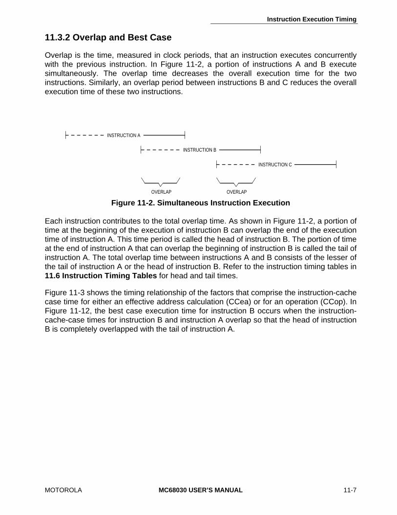
Instruction Execution Timing
MOTOROLA
MC68030 USER’S MANUAL
11-7
11.3.2 Overlap and Best Case
Overlap is the time, measured in clock periods, that an instruction executes concurrentlywith the previous instruction. In Figure 11-2, a portion of instructions A and B executesimultaneously. The overlap time decreases the overall execution time for the twoinstructions. Similarly, an overlap period between instructions B and C reduces the overallexecution time of these two instructions.
Each instruction contributes to the total overlap time. As shown in Figure 11-2, a portion oftime at the beginning of the execution of instruction B can overlap the end of the executiontime of instruction A. This time period is called the head of instruction B. The portion of timeat the end of instruction A that can overlap the beginning of instruction B is called the tail ofinstruction A. The total overlap time between instructions A and B consists of the lesser ofthe tail of instruction A or the head of instruction B. Refer to the instruction timing tables in
11.6 Instruction Timing Tables
for head and tail times.
Figure 11-3 shows the timing relationship of the factors that comprise the instruction-cachecase time for either an effective address calculation (CCea) or for an operation (CCop). InFigure 11-12, the best case execution time for instruction B occurs when the instruction-cache-case times for instruction B and instruction A overlap so that the head of instructionB is completely overlapped with the tail of instruction A.
Figure 11-2. Simultaneous Instruction Execution
INSTRUCTION A
INSTRUCTION B
INSTRUCTION C
OVERLAP OVERLAP
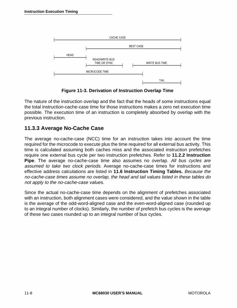
Instruction Execution Timing
11-8
MC68030 USER’S MANUAL
MOTOROLA
The nature of the instruction overlap and the fact that the heads of some instructions equalthe total instruction-cache-case time for those instructions makes a zero net execution timepossible. The execution time of an instruction is completely absorbed by overlap with theprevious instruction.
11.3.3 Average No-Cache Case
The average no-cache-case (NCC) time for an instruction takes into account the timerequired for the microcode to execute plus the time required for all external bus activity. Thistime is calculated assuming both caches miss and the associated instruction prefetchesrequire one external bus cycle per two instruction prefetches. Refer to
11.2.2 InstructionPipe
. The average no-cache-case time also assumes no overlap.
All bus cycles areassumed to take two clock periods
. Average no-cache-case times for instructions andeffective address calculations are listed in
11.6 Instruction Timing Tables.
Because theno-cache-case times assume no overlap, the head and tail values listed in these tables donot apply to the no-cache-case values
.
Since the actual no-cache-case time depends on the alignment of prefetches associatedwith an instruction, both alignment cases were considered, and the value shown in the tableis the average of the odd-word-aligned case and the even-word-aligned case (rounded upto an integral number of clocks). Similarly, the number of prefetch bus cycles is the averageof these two cases rounded up to an integral number of bus cycles.
Figure 11-3. Derivation of Instruction Overlap Time
CACHE CASE
BEST CASE
HEAD
MICROCODE TIME
TAIL
READ/WRITE BUSTIME OR SYNC WRITE BUS TIME

Instruction Execution Timing
MOTOROLA
MC68030 USER’S MANUAL
11-9
The effect of instruction alignment on timing is illustrated by the following example. Theassumptions referred to in
11.6 Instruction Timing Tables
apply. Both the data cache andinstruction cache miss on all accesses.
Instruction
1.MOVE.L (d
16
,An,Dn),Dn2.CMPI.W #<data>.W,(d
16
,An)
The instruction stream is positioned with even alignment in 32-bit memory as:
Figure 11-4 shows processor activity for even alignment of the given instruction stream. Itshows the activity of the external bus, the bus controller, and the sequencer.
Figure 11-5 shows processor activity for odd alignment. The instruction stream is positionedin 32-bit memory as:
Address n MOVE EA Extn+4 d
16
CMPI
n+8 #(data. W) d
16
n+12 ... ...
Figure 11-4. Processor Activity – Even Alignment
Address n ... MOVEn+4 EA Ext d
16
n+8 CMPI #(data.W)n+12 d
16
...
1 2 3 4 5 6 7 8 9 10 11 12 13 14 15 16
CLOCK
BUSACTIVITY
PREFETCH READ PREFETCH
BUSCONTROLLER
SEQUENCER
INSTRUCTIONEXECUTION TIME
CLOCKCOUNT
LEGEND:
2) #(data).W,(d ,An)
READ PREFETCH
IDLE PREFETCHn + 8
READ FROMd ,An,Dn16
CALCULATE AND FETCHSOURCE EAFOR MOVE
MOVE.L (d ,An,Dn),Dn16
IDLE READ FROM(d ,An)16
CALCULATE AND FETCHSOURCE EA
FOR CMPI
CMPI.W #(data).W,(d ,An)16
8
IDLEPREFETCHn + 16
IDLEPERFORM
CMPI
1) MOVE.L (d ,An,Dn),Dn16
16
PREFETCHn + 12
PERFORMMOVE
8

Instruction Execution Timing
11-10
MC68030 USER’S MANUAL
MOTOROLA
Comparing the two alignments, the execution time of the MOVE instruction is eight clocksfor even alignment and 10 clocks for odd alignment, an average of nine clocks. Referring tothe table in
11.6.6 MOVE Instruction
and the table in
11.6.1 Fetch Effective Address(fea)
, the average no-cache-case time is 2+7 = 9 clocks. A similar calculation can be madeof the CMPI instruction, which has an average no-cache-case time of seven clocks.
The average no-cache-case timing rather than the maximum no-cache-case timing gives acloser approximation of the actual timing of an instruction stream in many cases. The totalexecution time of the two instructions in the previous example is 16 clocks for both even andodd alignment. Adding the average no-cache-case timing of the given instructions also gives16 clocks (9+7 = 16 clocks). It should be noted again that the no-cache-case time assumesno overlap. Therefore, the actual execution time of an instruction stream may be less thanthat given by adding the no-cache-case times. To factor in the effect of wait states for theno-cache case, refer to
11.5 Effect of Wait States
.
11.3.4 Actual Instruction-Cache-Case Execution Time Calculations
The overall execution time for an instruction may depend on the overlap with the previousand following instructions. Therefore, to calculate instruction execution time estimations, theentire code sequence to be evaluated must be analyzed as a whole. To derive the actualinstruction-cache-case execution times for an instruction sequence (under the assumptionslisted in
11.6 Instruction Timing Tables)
, the instruction-cache-case times listed in thetables must be used, and the proper overlap must be subtracted for the entire sequence.The formula for this calculation is:
CC
1
+[CC
2
–min(H
2
,T
1
)]+[(CC
3
–min(H
3
,T
2
)]+. . . (11-1)
where:
Figure 11-5. Processor Activity – Odd Alignment
1 2 3 4 5 6 7 8 9 10 11 12 13 14 15 16
CLOCK
BUSACTIVITY
READ PREFETCH
BUSCONTROLLER
SEQUENCER
INSTRUCTIONEXECUTION TIME
CLOCKCOUNT
LEGEND:
2) #(data).W,(d ,An)
PREFETCHREADPREFETCH
IDLE IDLE
IDLE
READ FROMd ,An,Dn16
CALCULATE AND FETCHSOURCE EAFOR MOVE
MOVE.L (d ,An,Dn),Dn16
READ FROM(d ,An)16
CALCULATE AND FETCHSOURCE EA
FOR CMPI
CMPI.W #(data).W,(d ,An)16
10
PREFETCHn + 16
PREFETCHn + 12
PERFORMCMPI
1) MOVE.L (d ,An,Dn),Dn16
16
PREFETCHn + 8
PERFORMMOVE
6
Instruction Execution Timing
MOTOROLA
MC68030 USER’S MANUAL
11-11
CC
n
is the instruction-cache-case time for an instruction,
T
n
is the tail time for an instruction,
H
n
is the head time for an instruction, and
min(a,b) is the minimum of parameters a and b.
The instruction-cache-case time for most instructions is composed of the instruction-cache-case time for the effective address calculation (CCea) overlapped with the instruction-cache-case time for the operation (CCop). The more specific formula is:
CCea
1
+[CCop
1
–min(Hop
1
,Tea
1
)]+[CCea
2
–min(Hea
2
,Top
1
)]+[CCop
2
–min(Hop
2
,Tea
2
)]+[CCea
3
–min(Hea
3,
Top
2
)]+. . . (11-2)
where:
CCea
n
is the effective address time for the instruction-cache case,
CCop
n
is the instruction-cache-case time for the operation portion of an instruction,
Tea
n
is the tail time for the effective address of an instruction,
Hop
n
is the head time for the operation portion of an instruction,
Top
n is the tail time for the operation portion of an instruction,
Hean is the head time for the effective address of an instruction, and
min(a,b) is the minimum of parameters a and b.
Instruction Execution Timing
11-12 MC68030 USER’S MANUAL MOTOROLA
The instructions that require the instruction-cache case, head, and tail of an effectiveaddress (CCea, Hea, and Tea) to be overlapped with CCop, Hop, and Top are footnoted in11.6 Instruction Timing Tables.
The actual instruction-cache-case execution time for a stream of instructions can becomputed using Equation (11-1) or the general Equation (11-2). Equation (11-1) is usedunless the instruction-cache case, head, and tail of an effective address are required.
An example using a series of instructions that require Equation (11-1) to calculate theinstruction-cache-case execution time follows. The assumptions referred to in 11.6Instruction Timing Tables apply.
Instruction
1. ADD.L A1,D12. SUBA.L D1,A2
Referring to the timing table in 11.6.8 Arithmetical/Logical Instructions, the head, tail, andinstruction-cache-case (CC) times for ADD.L A1,D1 and SUBA.L D1,A2 are found. There isno footnote directing the user to add an effective address time for either instruction. Sinceboth of the instructions use register operands only, there is no need to add effective addresscalculation times. Therefore, the general Equation (11-1) can be used for both.
Head Tail CC
1.ADD.L A1,D1 2 0 22.SUBA.L D1,A2 4 0 4
NOTE
The underlined numbers show the typical pattern for the com-parison of head and tail in the following equation.
The following computations use Equation (11-1):
Execution Time = CC1+[CC2-min(H2,T1)] = 2+[4-min(4,0)] = 2+[4-0] = 6 clocks
Instruction Execution Timing
MOTOROLA MC68030 USER’S MANUAL 11-13
Instructions that require the addition of an effective address calculation time from anappropriate table use the general Equation (11-2) to calculate the actual CC time. TheCCea, Hea, and Tea values must be extracted from the appropriate effective address table(either fetch effective address, fetch immediate effective address, calculate effectiveaddress, calculate immediate effective address, or jump effective address) as indicated andincluded in Equation (11-2). All of the following instructions (except the last) require generalEquation (11-2). The last instruction uses Equation (11-1).
Instruction
1. ADD.L -(A1),D1 2. AND.L D1,([A2]) 3. MOVE.L (A6),(8,A1) 4. TAS (A3)+ 5. NEG D3
Using the appropriate operation and effective address tables from 11.6 Instruction TimingTables:
Head Tail CC
1. ADD.L -(A1),D1Fetch Effective Address (fea) -(An) 2 2 4ADD EA,Dn 0 0 2
2. AND.L D1,(A2)fea ([B]) 4 0 10AND Dn,EA 0 1 3
3. MOVE.L (A6),(8,A1)fea (An) 1 1 3MOVE Source,(d 16,An) 2 0 4
4. TAS (A3)+Calculate Effective Address (cea) (An)+ 0 0 2TAS Mem 3 0 12
5. NEG D3 2 0 2
The following calculations use Equations (11-1) and (11-2):
ExecutionTime = CCea1+[CCop1-min(Hop1,Tea1)]+[CCea2-min(Hea2,Top1)]+[CCop2-min(Hop2,Tea2)]+[CCea3-min(Hea3,Top2)]+[CCop3-min(Hop3,Tea3)]+[CCea4-min(Hop4,Top3)]+[CCop4-min(Hop4,Top3)]+[CCop5-min(Hop5,Top4)]
= 4+[2-min(0,2)]+[10-min(4,0)]+[3-min(0,0)]+[3-min(1,1)]+ = [4-min(2,1)]+[2-min(0,0)]+[12-min(3,0)]+[2-min(2,0)] = 4+2+10+3+2+3+2+12+2 = 40 clock periods
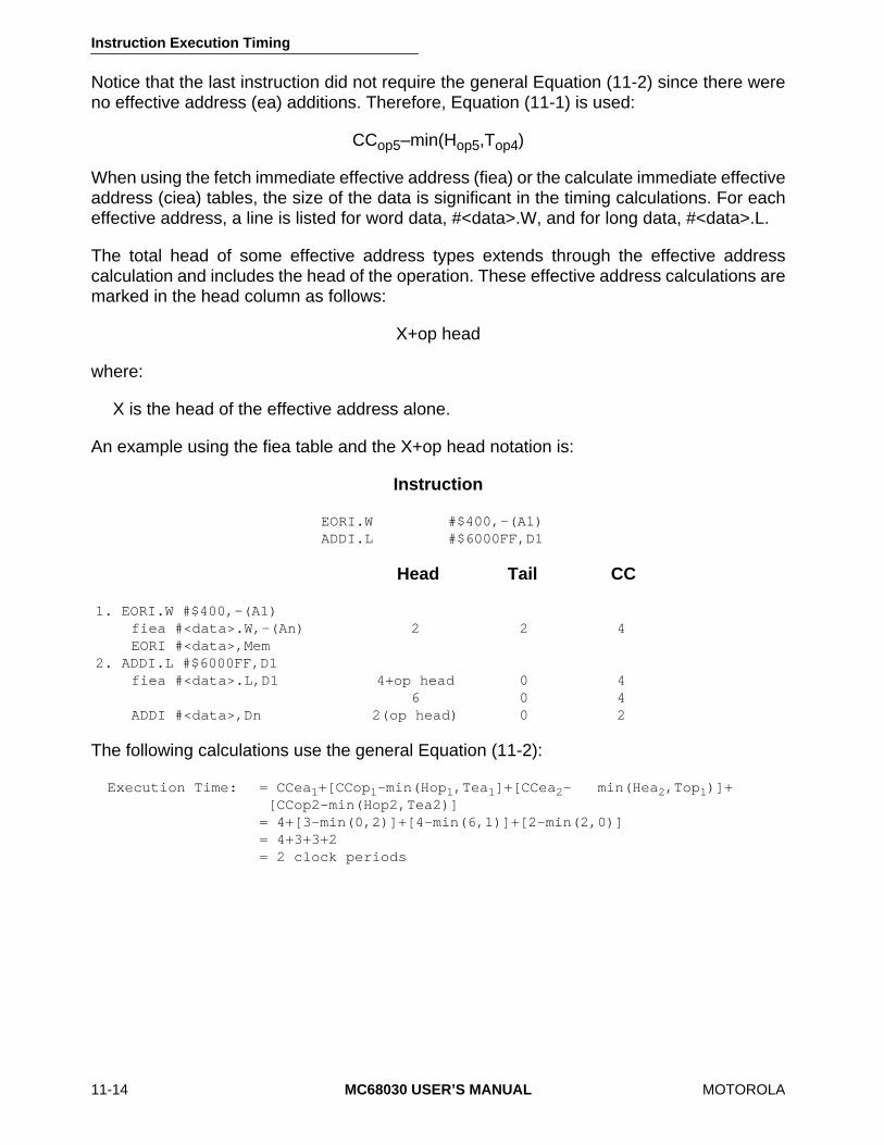
Instruction Execution Timing
11-14 MC68030 USER’S MANUAL MOTOROLA
Notice that the last instruction did not require the general Equation (11-2) since there wereno effective address (ea) additions. Therefore, Equation (11-1) is used:
CCop5–min(Hop5,Top4)
When using the fetch immediate effective address (fiea) or the calculate immediate effectiveaddress (ciea) tables, the size of the data is significant in the timing calculations. For eacheffective address, a line is listed for word data, #<data>.W, and for long data, #<data>.L.
The total head of some effective address types extends through the effective addresscalculation and includes the head of the operation. These effective address calculations aremarked in the head column as follows:
X+op head
where:
X is the head of the effective address alone.
An example using the fiea table and the X+op head notation is:
Instruction
EORI.W #$400,-(A1) ADDI.L #$6000FF,D1
Head Tail CC
1. EORI.W #$400,-(A1)fiea #<data>.W,-(An) 2 2 4EORI #<data>,Mem
2. ADDI.L #$6000FF,D1fiea #<data>.L,D1 4+op head 0 4
6 0 4ADDI #<data>,Dn 2(op head) 0 2
The following calculations use the general Equation (11-2):
Execution Time: = CCea1+[CCop1-min(Hop1,Tea1]+[CCea2- min(Hea2,Top1)]+[CCop2-min(Hop2,Tea2)]
= 4+[3-min(0,2)]+[4-min(6,1)]+[2-min(2,0)] = 4+3+3+2 = 2 clock periods
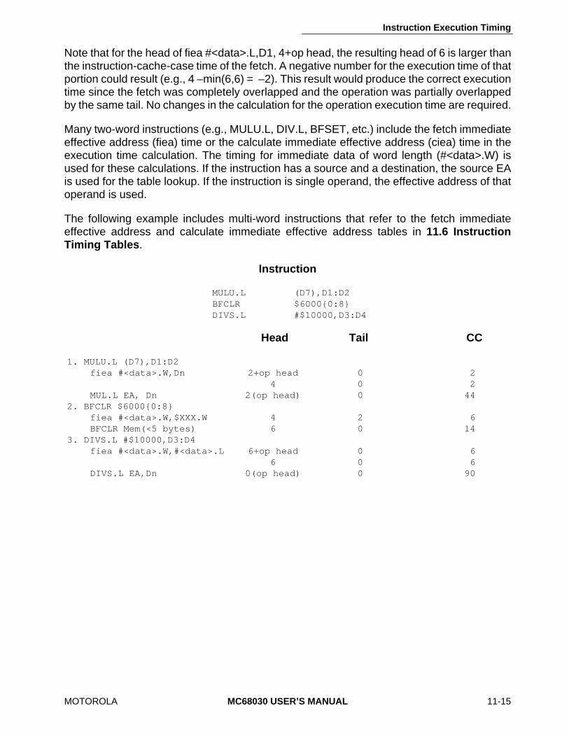
Instruction Execution Timing
MOTOROLA MC68030 USER’S MANUAL 11-15
Note that for the head of fiea #<data>.L,D1, 4+op head, the resulting head of 6 is larger thanthe instruction-cache-case time of the fetch. A negative number for the execution time of thatportion could result (e.g., 4 –min(6,6) = –2). This result would produce the correct executiontime since the fetch was completely overlapped and the operation was partially overlappedby the same tail. No changes in the calculation for the operation execution time are required.
Many two-word instructions (e.g., MULU.L, DIV.L, BFSET, etc.) include the fetch immediateeffective address (fiea) time or the calculate immediate effective address (ciea) time in theexecution time calculation. The timing for immediate data of word length (#<data>.W) isused for these calculations. If the instruction has a source and a destination, the source EAis used for the table lookup. If the instruction is single operand, the effective address of thatoperand is used.
The following example includes multi-word instructions that refer to the fetch immediateeffective address and calculate immediate effective address tables in 11.6 InstructionTiming Tables.
Instruction
MULU.L (D7),D1:D2 BFCLR $6000{0:8} DIVS.L #$10000,D3:D4
Head Tail CC
1. MULU.L (D7),D1:D2fiea #<data>.W,Dn 2+op head 0 2
4 0 2MUL.L EA, Dn 2(op head) 0 44
2. BFCLR $6000{0:8}fiea #<data>.W,$XXX.W 4 2 6BFCLR Mem(<5 bytes) 6 0 14
3. DIVS.L #$10000,D3:D4fiea #<data>.W,#<data>.L 6+op head 0 6
6 0 6DIVS.L EA,Dn 0(op head) 0 90
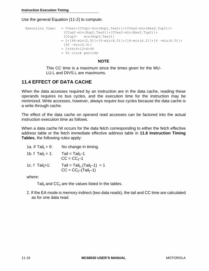
Instruction Execution Timing
11-16 MC68030 USER’S MANUAL MOTOROLA
Use the general Equation (11-2) to compute:
Execution Time: = CCea1+[CCop1-min(Hop1,Tea1)]+[CCea2-min(Hea2,Top1)]+ [CCop2-min(Hop2,Tea2)]+[CCea3-min(Hea3,Top2)]+[CCop3- min(Hop3,Tea3)]
= 2+[44-min(2,0)]+[6-min(4,0)]+[14-min(6,2)]+[6 -min(6,0)]+[90 -min(0,0)]
= 2+44+6+12+6+90 = 60 clock periods
NOTE
This CC time is a maximum since the times given for the MU-LU.L and DIVS.L are maximums.
11.4 EFFECT OF DATA CACHE
When the data accesses required by an instruction are in the data cache, reading theseoperands requires no bus cycles, and the execution time for the instruction may beminimized. Write accesses, however, always require bus cycles because the data cache isa write through cache.
The effect of the data cache on operand read accesses can be factored into the actualinstruction execution time as follows.
When a data cache hit occurs for the data fetch corresponding to either the fetch effectiveaddress table or the fetch immediate effective address table in 11.6 Instruction TimingTables, the following rules apply:
1a. if Tailt = 0: No change in timing.
1b. f Tailt = 1: Tail = Tailt–1CC = CCt–1
1c. f Tailt>1: Tail = Tailt–(Tailt–1) = 1CC = CCt–(Tailt–1)
where:
Tailt and CCt are the values listed in the tables.
2. If the EA mode is memory indirect (two data reads), the tail and CC time are calculatedas for one data read.
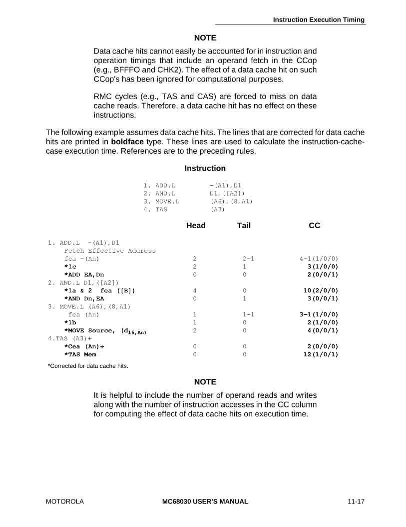
Instruction Execution Timing
MOTOROLA MC68030 USER’S MANUAL 11-17
NOTE
Data cache hits cannot easily be accounted for in instruction andoperation timings that include an operand fetch in the CCop(e.g., BFFFO and CHK2). The effect of a data cache hit on suchCCop's has been ignored for computational purposes.
RMC cycles (e.g., TAS and CAS) are forced to miss on datacache reads. Therefore, a data cache hit has no effect on theseinstructions.
The following example assumes data cache hits. The lines that are corrected for data cachehits are printed in boldface type. These lines are used to calculate the instruction-cache-case execution time. References are to the preceding rules.
Instruction
1. ADD.L -(A1),D12. AND.L D1,([A2])3. MOVE.L (A6),(8,A1)4. TAS (A3)
Head Tail CC
1. ADD.L -(A1),D1Fetch Effective Addressfea -(An) 2 2-1 4-1(1/0/0)*1c 2 1 3(1/0/0)*ADD EA,Dn 0 0 2(0/0/1)
2. AND.L D1,([A2])*1a & 2 fea ([B]) 4 0 10(2/0/0)*AND Dn,EA 0 1 3(0/0/1)
3. MOVE.L (A6),(8,A1) fea (An) 1 1-1 3–1(1/0/0)*1b 1 0 2(1/0/0)*MOVE Source, (d16,An) 2 0 4(0/0/1)
4.TAS (A3)+*Cea (An)+ 0 0 2(0/0/0)*TAS Mem 0 0 12(1/0/1)
*Corrected for data cache hits.
NOTE
It is helpful to include the number of operand reads and writesalong with the number of instruction accesses in the CC columnfor computing the effect of data cache hits on execution time.
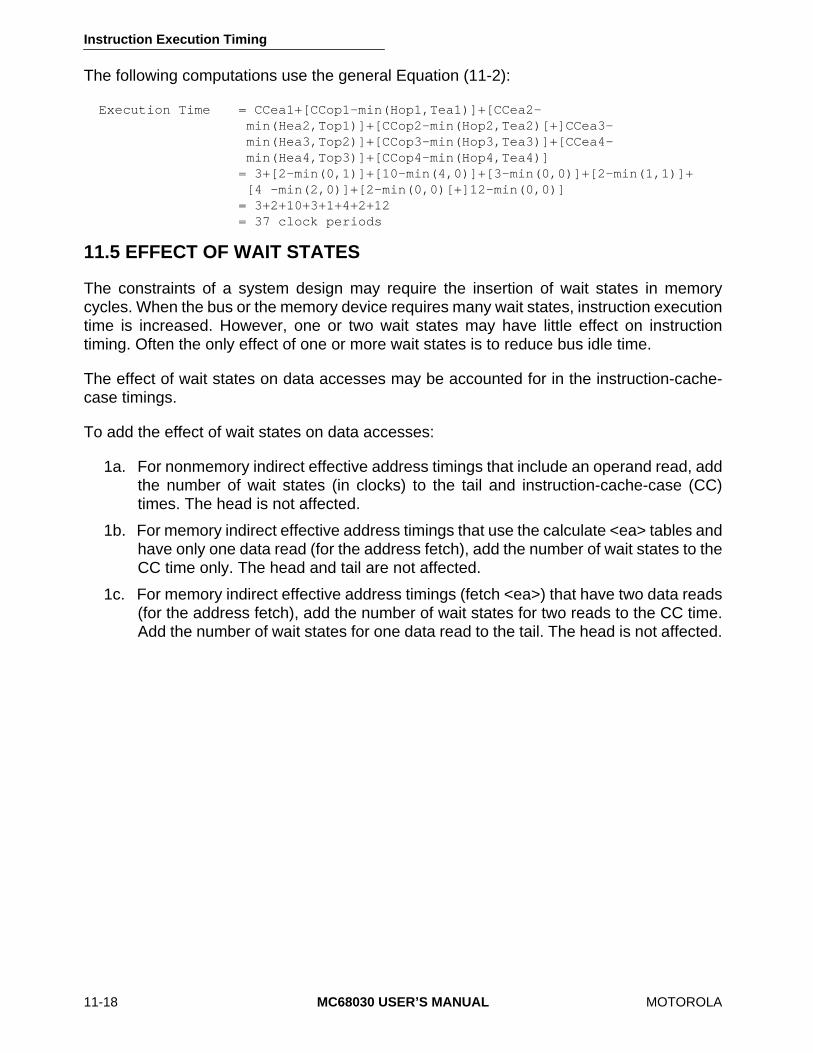
Instruction Execution Timing
11-18 MC68030 USER’S MANUAL MOTOROLA
The following computations use the general Equation (11-2):
Execution Time = CCea1+[CCop1-min(Hop1,Tea1)]+[CCea2- min(Hea2,Top1)]+[CCop2-min(Hop2,Tea2)[+]CCea3- min(Hea3,Top2)]+[CCop3-min(Hop3,Tea3)]+[CCea4- min(Hea4,Top3)]+[CCop4-min(Hop4,Tea4)]
= 3+[2-min(0,1)]+[10-min(4,0)]+[3-min(0,0)]+[2-min(1,1)]+[4 -min(2,0)]+[2-min(0,0)[+]12-min(0,0)]
= 3+2+10+3+1+4+2+12 = 37 clock periods
11.5 EFFECT OF WAIT STATES
The constraints of a system design may require the insertion of wait states in memorycycles. When the bus or the memory device requires many wait states, instruction executiontime is increased. However, one or two wait states may have little effect on instructiontiming. Often the only effect of one or more wait states is to reduce bus idle time.
The effect of wait states on data accesses may be accounted for in the instruction-cache-case timings.
To add the effect of wait states on data accesses:
1a. For nonmemory indirect effective address timings that include an operand read, addthe number of wait states (in clocks) to the tail and instruction-cache-case (CC)times. The head is not affected.
1b. For memory indirect effective address timings that use the calculate <ea> tables andhave only one data read (for the address fetch), add the number of wait states to theCC time only. The head and tail are not affected.
1c. For memory indirect effective address timings (fetch <ea>) that have two data reads(for the address fetch), add the number of wait states for two reads to the CC time.Add the number of wait states for one data read to the tail. The head is not affected.
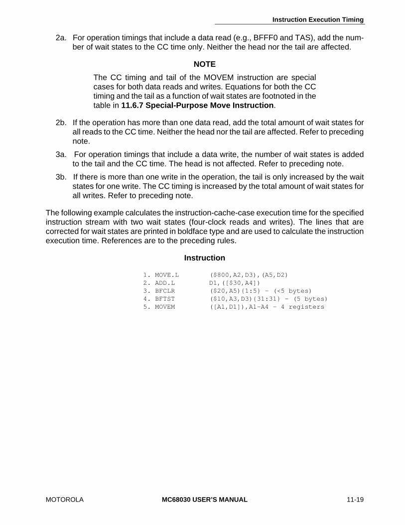
Instruction Execution Timing
MOTOROLA MC68030 USER’S MANUAL 11-19
2a. For operation timings that include a data read (e.g., BFFF0 and TAS), add the num-ber of wait states to the CC time only. Neither the head nor the tail are affected.
NOTE
The CC timing and tail of the MOVEM instruction are specialcases for both data reads and writes. Equations for both the CCtiming and the tail as a function of wait states are footnoted in thetable in 11.6.7 Special-Purpose Move Instruction.
2b. If the operation has more than one data read, add the total amount of wait states forall reads to the CC time. Neither the head nor the tail are affected. Refer to precedingnote.
3a. For operation timings that include a data write, the number of wait states is addedto the tail and the CC time. The head is not affected. Refer to preceding note.
3b. If there is more than one write in the operation, the tail is only increased by the waitstates for one write. The CC timing is increased by the total amount of wait states forall writes. Refer to preceding note.
The following example calculates the instruction-cache-case execution time for the specifiedinstruction stream with two wait states (four-clock reads and writes). The lines that arecorrected for wait states are printed in boldface type and are used to calculate the instructionexecution time. References are to the preceding rules.
Instruction
1. MOVE.L ($800,A2,D3),(A5,D2)2. ADD.L D1,([$30,A4])3. BFCLR ($20,A5){1:5} - (<5 bytes)4. BFTST ($10,A3,D3){31:31} - (5 bytes)5. MOVEM ([A1,D1]),A1-A4 - 4 registers
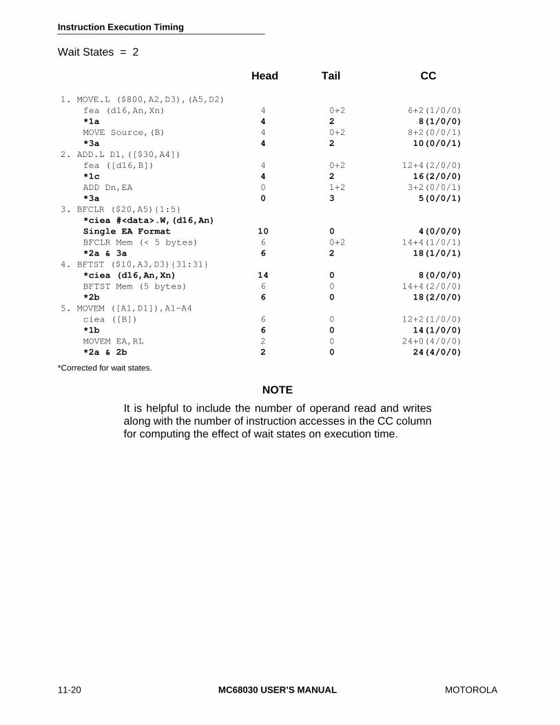
Instruction Execution Timing
11-20 MC68030 USER’S MANUAL MOTOROLA
Wait States = 2
Head Tail CC
1. MOVE.L ($800,A2,D3),(A5,D2)fea (d16,An,Xn) 4 0+2 6+2(1/0/0)*1a 4 2 8(1/0/0)MOVE Source,(B) 4 0+2 8+2(0/0/1)*3a 4 2 10(0/0/1)
2. ADD.L D1,([$30,A4])fea ([d16,B]) 4 0+2 12+4(2/0/0)*1c 4 2 16(2/0/0)ADD Dn,EA 0 1+2 3+2(0/0/1)*3a 0 3 5(0/0/1)
3. BFCLR ($20,A5){1:5}*ciea #<data>.W,(d16,An)Single EA Format 10 0 4(0/0/0)BFCLR Mem (< 5 bytes) 6 0+2 14+4(1/0/1)*2a & 3a 6 2 18(1/0/1)
4. BFTST ($10,A3,D3){31:31}*ciea (d16,An,Xn) 14 0 8(0/0/0)BFTST Mem (5 bytes) 6 0 14+4(2/0/0) *2b 6 0 18(2/0/0)
5. MOVEM ([A1,D1]),A1-A4ciea ([B]) 6 0 12+2(1/0/0)*1b 6 0 14(1/0/0)MOVEM EA,RL 2 0 24+0(4/0/0)*2a & 2b 2 0 24(4/0/0)
*Corrected for wait states.
NOTE
It is helpful to include the number of operand read and writesalong with the number of instruction accesses in the CC columnfor computing the effect of wait states on execution time.
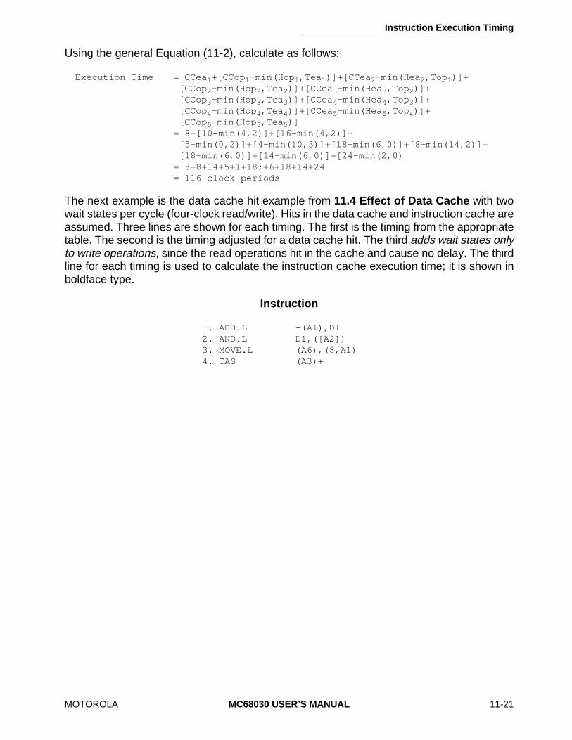
Instruction Execution Timing
MOTOROLA MC68030 USER’S MANUAL 11-21
Using the general Equation (11-2), calculate as follows:
Execution Time = CCea1+[CCop1-min(Hop1,Tea1)]+[CCea2-min(Hea2,Top1)]+[CCop2-min(Hop2,Tea2)]+[CCea3-min(Hea3,Top2)]+[CCop3-min(Hop3,Tea3)]+[CCea4-min(Hea4,Top3)]+[CCop4-min(Hop4,Tea4)]+[CCea5-min(Hea5,Top4)]+[CCop5-min(Hop5,Tea5)]
= 8+[10-min(4,2)]+[16-min(4,2)]+[5-min(0,2)]+[4-min(10,3)]+[18-min(6,0)]+[8-min(14,2)]+[18-min(6,0)]+[14-min(6,0)]+[24-min(2,0)
= 8+8+14+5+1+18;+6+18+14+24 = 116 clock periods
The next example is the data cache hit example from 11.4 Effect of Data Cache with twowait states per cycle (four-clock read/write). Hits in the data cache and instruction cache areassumed. Three lines are shown for each timing. The first is the timing from the appropriatetable. The second is the timing adjusted for a data cache hit. The third adds wait states onlyto write operations, since the read operations hit in the cache and cause no delay. The thirdline for each timing is used to calculate the instruction cache execution time; it is shown inboldface type.
Instruction
1. ADD.L -(A1),D12. AND.L D1,([A2])3. MOVE.L (A6),(8,A1)4. TAS (A3)+
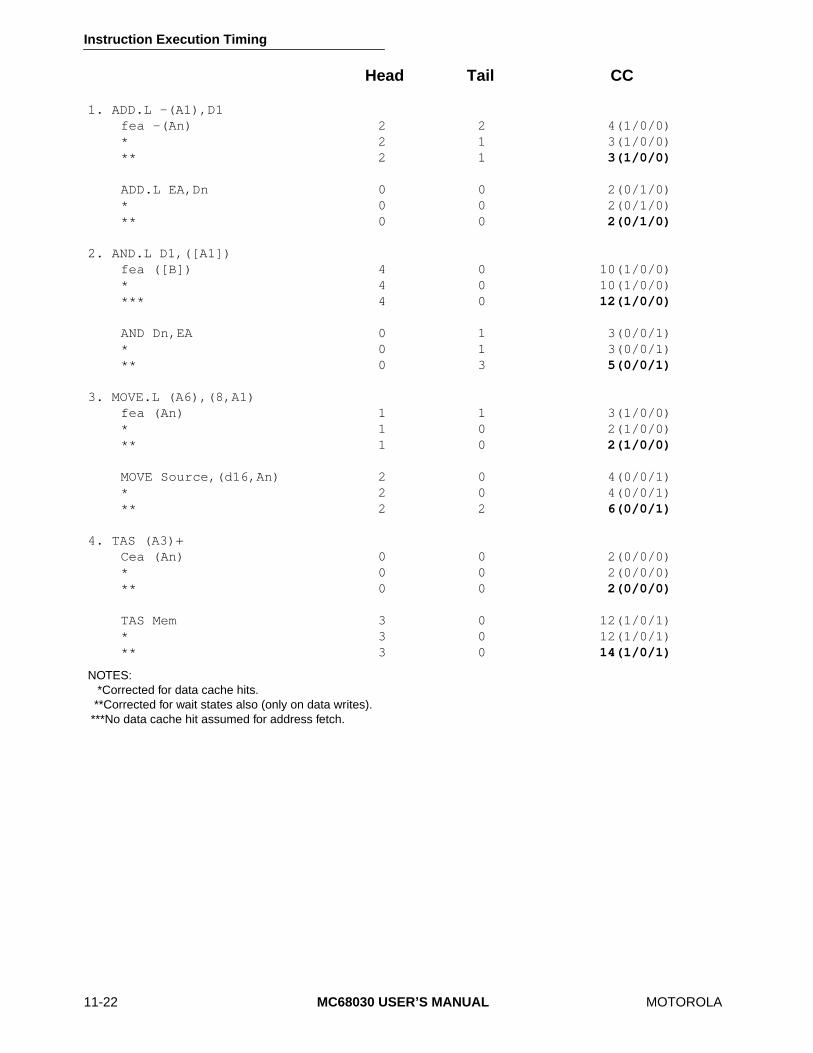
Instruction Execution Timing
11-22 MC68030 USER’S MANUAL MOTOROLA
Head Tail CC
1. ADD.L -(A1),D1fea -(An) 2 2 4(1/0/0)* 2 1 3(1/0/0)** 2 1 3(1/0/0)
ADD.L EA,Dn 0 0 2(0/1/0)* 0 0 2(0/1/0)** 0 0 2(0/1/0)
2. AND.L D1,([A1])fea ([B]) 4 0 10(1/0/0)* 4 0 10(1/0/0)*** 4 0 12(1/0/0)
AND Dn,EA 0 1 3(0/0/1)* 0 1 3(0/0/1)** 0 3 5(0/0/1)
3. MOVE.L (A6),(8,A1)fea (An) 1 1 3(1/0/0)* 1 0 2(1/0/0)** 1 0 2(1/0/0)
MOVE Source,(d16,An) 2 0 4(0/0/1)* 2 0 4(0/0/1)** 2 2 6(0/0/1)
4. TAS (A3)+Cea (An) 0 0 2(0/0/0)* 0 0 2(0/0/0)** 0 0 2(0/0/0)
TAS Mem 3 0 12(1/0/1)* 3 0 12(1/0/1)** 3 0 14(1/0/1)
NOTES: *Corrected for data cache hits. **Corrected for wait states also (only on data writes).***No data cache hit assumed for address fetch.

Instruction Execution Timing
MOTOROLA MC68030 USER’S MANUAL 11-23
Using the general Equation (11-2), calculate as follows:
Execution Time = CCea1+[CCop1-min(Hea1,Top1)]+[CCea2-min(Hea2,Top1)]+[CCop2-min(Hop2,Tea2)]+[CCea3-min(Hea3,Top2)]+[CCop3-min(Hop3,Tea3)]+[CCea4-min(Hea4,Top3)]+[CCop4-min(Hop4,Tea4)]
= 3+[2-min(0,1)]m+[12-min(4,0)]+[5-min(0,0)]+[2-min(1,3)]+[6-min(2,0)]+[2-min(0,2)]+[14-min(3,0)
= 3+2+12+5+1+6+2+14 = 45 clock periods
A similar analysis can be constructed for the average no-cache case. Since the average no-cache-case time assumes two clock periods per bus cycle (i.e., no wait states), the timinggiven in the tables does not apply directly to systems with wait states. To approximate theaverage no-cache-case time for an instruction or effective address with W wait states, usethe following formula:
NCC = NCCt+(# of data reads and writes)•W+(max. # of instruction accesses)•W
where:
NCCt is the no-cache-case timing value from the appropriate table.
The number of data reads, data writes, and maximum instruction accesses are found inthe appropriate table.
The average no-cache-case timing obtained from this formula is equal to or greater than theactual no-cache-case timing since the number of instruction accesses used is a maximum(the values in the tables are always rounded up) and no overlap is assumed.

Instruction Execution Timing
11-24 MC68030 USER’S MANUAL MOTOROLA
11.6 INSTRUCTION TIMING TABLES
All the following assumptions apply to the times shown in the tables in this section:
• All memory accesses occur with two-clock bus cycles and no wait states.
• All operands in memory, including the system stack, are long-word aligned.
• A 32-bit bus is used for communications between the MC68030 and system memory.
• The data cache is not enabled.
• No exceptions occur (except as specified).
• Required address translations for all external bus cycles are resident in the address translation cache.
Four values are listed for each instruction and effective address:
1. Head,
2. Tail,
3. Instruction-cache case (CC) when the instruction is in the cache but has no overlap, and
4. Average no-cache case (NCC) when the instruction is not in the cache or the cache is disabled and there is no instruction overlap.
The only instances for which the size of the operand has any effect are the instructions withimmediate operands and the ADDA and SUBA instructions. Unless specified otherwise,immediate byte and word operands have identical execution times.

Instruction Execution Timing
MOTOROLA MC68030 USER’S MANUAL 11-25
The instruction-cache-case and average no-cache-case columns of the instruction timingtables contain four sets of numbers, three of which are enclosed in parentheses. The outernumber is the total number of clocks for the given cache case and instruction. The firstnumber inside the parentheses is the number of operand read cycles performed by theinstruction. The second value inside the parentheses is the maximum number of instructionbus cycles performed by the instruction, including all prefetches to keep the instruction pipefilled. Because the second value is the average of the odd-word-aligned case and the even-word-aligned case (rounded up to an integral number of bus cycles), it is always greater thanor equal to the actual number of bus cycles (one bus cycle per two instruction prefetches).The third value within the parentheses is the number of write cycles performed by theinstruction. One example from the instruction timing table is:
The total numbers of bus-activity clocks and internal clocks (not overlapped by bus activity)of the instruction in this example are derived as follows:
(2 Reads•2 Clocks/Read)+l(3 Instruction Accesses•2 Clocks/Access)+(0 Writes•2 Clocks/Write) = 10 Clocks of Bus Activity
21 Total Clocks–10 Bus Activity Clocks = 11 Internal Clocks
The example used here is taken from a no-cache-case ‘fetch effective address' time. Theaddressing mode is ([d32,B],I,d32). The same addressing mode under the instruction-cache-case execution time entry is 18(2/0/0). For the instruction-cache-case execution time,no instruction accesses are required because the cache is enabled and the sequencer doesnot have to access external memory for the instruction words.
The first five timing tables deal exclusively with fetching and calculating effective addressesand immediate operands. The remaining tables are instruction and operation timings. Someinstructions use addressing modes that are not included in the corresponding instructiontimings. These cases refer to footnotes that indicate the additional table needed for thetiming calculation. All read and write accesses are assumed to take two clock periods.
11.6.1 Fetch Effective Address (fea)
The fetch effective address table indicates the number of clock periods needed for theprocessor to calculate and fetch the specified effective address. The effective addresses aredivided by their formats (refer to 2.5 Effective Address Encoding Summary). Forinstruction-cache case and for no-cache case, the total number of clock cycles is outside theparentheses. The number of read, prefetch, and write cycles is given inside the parenthesesas (r/p/w). The read, prefetch, and write cycles are included in the total clock cycle number.
TOTAL NUMBER OF CLOCKS
NUMBER OF READ CYCLES
MAXIMUM NUMBER OF INSTRUCTION ACCESS CYCLES
NUMBER OF WRITE CYCLES
21 (2 3 0)/ /

Instruction Execution Timing
11-26 MC68030 USER’S MANUAL MOTOROLA
All timing data assumes two-clock reads and writes.
Address Mode Head Tail I-Cache Case No-Cache Case
SINGLE EFFECTIVE ADDRESS INSTRUCTION FORMAT
% Dn – – 0(0/0/0) 0(0/0/0)% An – – 0(0/0/0) 0(0/0/0)
(An) 1 1 3(1/0/0) 3(1/0/0)(An)+ 0 1 3(1/0/0) 3(1/0/0)–(An) 2 2 4(1/0/0) 4(1/0/0)(d16,An) or (d16,PC) 2 2 4(1/0/0) 4(1/1/0)
(xxx).W 2 2 4(1/0/0) 4(1/1/0)(xxx).L 1 0 4(1/0/0) 5(1/1/0)#⟨data⟩.B 2 0 2(0/0/0) 2(0/1/0)#⟨data⟩.W 2 0 2(0/0/0) 2(0/1/0)#⟨data⟩.L 4 0 4(0/0/0) 4(0/1/0)
BRIEF FORMAT EXTENSION WORD
( d8,An,Xn) or ( d8,PC,Xn) 4 2 6(1/0/0) 6(1/1/0)

Instruction Execution Timing
MOTOROLA MC68030 USER’S MANUAL 11-27
11.6.1 Fetch Effective Address (fea) (Continued)
B = Base Address; 0, An, PC, Xn, An+Xn, PC+Xn. Form does not affect timing.I = Index; 0, Xn% = No clock cycles incurred by effective address fetch.NOTE: Xn cannot be in B and I at the same time. Scaling and size of Xn do not affect timing.
Address Mode Head Tail I-Cache Case No-Cache Case
FULL FORMAT EXTENSION WORD(S)
(d16,An) or (d16,PC) 2 0 6(1/0/0) 7(1/1/0)
(d16,An,Xn) or (d16,PC,Xn) 4 0 6(1/0/0) 7(1/1/0)
([d16,An]) or ([d16,PC]) 2 0 10(2/0/0) 10(2/1/0)
([d16,An],Xn) or ([d16,PC],Xn) 2 0 10(2/0/0) 10(2/1/0)
[d16,An],d16) or ([d16,PC],d16) 2 0 12(2/0/0) 13(2/2/0)
([d16,An],Xn,d16) or ([d16,PC],Xn,d16) 2 0 12(2/0/0) 13(2/2/0)
([d16,An],d32) or ([d16,PC],d32) 2 0 12(2/0/0) 14(2/2/0)
([d16,An],Xn,d32) or ([d16,PC],Xn,d32) 2 0 12(2/0/0) 14(2/2/0)
(B) 4 0 6(1/0/0) 7(1/1/0)(d16,B) 4 0 8(1/0/0) 10(1/1/0)
(d32,B) 4 0 12(1/0/0) 13(1/2/0)
([B]) 4 0 10(2/0/0) 10(2/1/0)([B],I) 4 0 10(2/0/0) 10(2/1/0)([B],d16) 4 0 12(2/0/0) 13(2/1/0)
([B],I,d16) 4 0 12(2/0/0) 13(2/1/0)
([B],d32) 4 0 12(2/0/0) 14(2/2/0)
([B],I,d32) 4 0 12(2/0/0) 14(2/2/0)
([d16,B]) 4 0 12(2/0/0) 13(2/1/0)
([d16,B],I) 4 0 12(2/0/0) 13(2/1/0)
([d16,B],d16) 4 0 14(2/0/0) 16(2/2/0)
([d16B],I,d16) 4 0 14(2/0/0) 16(2/2/0)
([d16,B],d32) 4 0 14(2/0/0) 17(2/2/0)
([d16,B\,I,d32) 4 0 14(2/0/0) 17(2/2/0)
([d32,B]) 4 0 16(2/0/0) 17(2/2/0)
([d32,B],I) 4 0 16(2/0/0) 17(2/2/0)
([d32,B],d16) 4 0 18(2/0/0) 20(2/2/0)
([d32,B],I,d16) 4 0 18(2/0/0) 20(2/2/0)
([d32,B],d32) 4 0 18(2/0/0) 21(2/3/0)
([d32,B],I,d32) 4 0 18(2/0/0) 21(2/3/0)

Instruction Execution Timing
11-28 MC68030 USER’S MANUAL MOTOROLA
11.6.2 Fetch Immediate Effective Address (fiea)
The fetch immediate effective address table indicates the number of clock periods neededfor the processor to fetch the immediate source operand and to calculate and fetch thespecified destination operand. In the case of two-word instructions, this table indicates thenumber of clock periods needed for the processor to fetch the second word of the instructionand to calculate and fetch the specified source operand or single operand. The effectiveaddresses are divided by their formats (refer to 2.5 Effective Address EncodingSummary). For instruction-cache case and for no-cache case, the total number of clockcycles is outside the parentheses. The number of read, prefetch, and write cycles is giveninside the parentheses as (r/p/w). The read, prefetch, and write cycles are included in thetotal clock cycle number.
All timing data assumes two-clock reads and writes.
Address Mode Head Tail I-Cache Case No-Cache Case
SINGLE EFFECTIVE ADDRESS INSTRUCTION FORMAT
% #⟨data⟩. W, Dn 2+op head 0 2(0/0/0) 2(0/1/0)% #⟨data⟩. L, Dn 4+op head 0 4(0/0/0) 4(0/1/0)
#⟨data⟩.W,(An) 1 1 3(1/0/0) 4(1/1/0)#⟨data⟩.L,(An) 1 0 4(1/0/0) 5(1/1/0)#⟨data⟩.W,(An)+ 2 1 5(1/0/0) 5(1/1/0)#⟨data⟩.L,(An)+ 4 1 7(1/0/0) 7(1/1/0)#⟨data⟩.W,–(An) 2 2 4(1/0/0) 4(1/1/0)#⟨data⟩.L,–(An) 2 0 4(1/0/0) 5(1/1/0)#⟨data⟩.W,(d16,An) 2 0 4(1/0/0) 5(1/1/0)
#⟨data⟩.L,(d16,An) 4 0 6(1/0/0) 8(1/2/0)
#⟨data⟩.W,$XXX.W 4 2 6(1/0/0) 6(1/1/0)#⟨data⟩.L,$XXX.W 6 2 8(1/0/0) 8(1/2/0)#⟨data⟩.W,$XXX.L 3 0 6(1/0/0) 7(1/2/0)#⟨data⟩.L,$XXX.L 5 0 8(1/0/0) 9(1/2/0)# ⟨data⟩.W, #⟨data⟩. L 6+op head 0 6(0/0/0) 6(0/2/0)
BRIEF FORMAT EXTENSION WORD
#⟨data⟩.W,(d8,An,Xn) or (d8,PC,Xn) 6 2 8(1/0/0) 8(1/2/0)
#⟨data⟩.L,(d8,An,Xn) or (d8,PC,Xn) 8 2 10(1/0/0) 10(1/2/0)
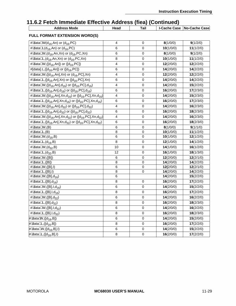
Instruction Execution Timing
MOTOROLA MC68030 USER’S MANUAL 11-29
11.6.2 Fetch Immediate Effective Address (fiea) (Continued)Address Mode Head Tail I-Cache Case No-Cache Case
FULL FORMAT EXTENSION WORD(S)
#⟨data⟩.W(d16,An) or (d16,PC) 4 0 8(1/0/0) 9(1/2/0)
#⟨data⟩.L(d16,An) or (d16,PC) 6 0 10(1/0/0) 11(1/2/0)
#⟨data⟩.W,(d16,An,Xn) or (d16,PC,Xn) 6 0 8(1/0/0) 9(1/2/0)
#⟨data⟩.L,(d16,An,Xn) or (d16,PC,Xn) 8 0 10(1/0/0) 11(1/2/0)
#⟨data⟩.W,([d16,An]) or ([d16,PC]) 4 0 12(2/0/0) 12(2/2/0)
#[data].L,([d16,An]) or ([d16,PC]) 6 0 14(2/0/0) 14(2/2/0)
#⟨data⟩.W,([d16,An],Xn) or (d16,PC],Xn) 4 0 12(2/0/0) 12(2/2/0)
#⟨data⟩.L,([d16,An],Xn) or ([d16,PC],Xn) 6 0 14(2/0/0) 14(2/2/0)
#⟨data⟩.W,([d16,An],d16) or ([d16,PC],d16) 4 0 14(2/0/0) 15(2/2/0)
#⟨data⟩.L,([d16,An],d16) or ([d16,PC],d16) 6 0 16(2/0/0) 17(2/3/0)
#⟨data⟩.W,([d16,An],Xn,d16) or ([d16,PC],Xn,d16) 4 0 14(2/0/0) 15(2/3/0)
#⟨data⟩.L,([d16,An],Xn,d16) or ([d16,PC],Xn,d16) 6 0 16(2/0/0) 17(2/3/0)
#⟨data⟩.W,([d16,An],d32) or ([d16,PC],d32) 4 0 14(2/0/0) 16(2/3/0)
#⟨data⟩.L,([d16,An],d32) or ([d16,PC],d32) 6 0 16(2/0/0) 18(2/3/0)
#⟨data⟩.W,([d16,An],Xn,d32) or ([d16,PC],Xn,d32) 4 0 14(2/0/0) 16(2/3/0)
#⟨data⟩.L,([d16,An],Xn,d32) or ([d16,PC],Xn,d32) 6 0 16(2/0/0) 18(2/3/0)
#⟨data⟩.W,(B) 6 0 8(1/0/0) 9(1/1/0)#⟨data⟩.L,(B) 8 0 10(1/0/0) 11(1/2/0)#⟨data⟩.W,(d16,B) 6 0 10(1/0/0) 12(1/2/0)
#⟨data⟩.L,(d16,B) 8 0 12(1/0/0) 14(1/2/0)
#⟨data⟩.W,(d32,B) 10 0 14(1/0/0) 16(1/2/0)
#⟨data⟩.L,(d32,B) 12 0 16(1/0/0) 18(1/3/0)
#⟨data⟩.W,([B]) 6 0 12(2/0/0) 12(2/1/0)#⟨data⟩.L,([B]) 8 0 14(2/0/0) 14(2/2/0)#⟨data⟩.W,([B],I) 6 0 12(2/0/0) 12(2/1/0)#⟨data⟩.L,([B],I) 8 0 14(2/0/0) 14(2/2/0)#⟨data⟩.W,([B],d16) 6 14(2/0/0) 15(2/2/0)
#⟨data⟩.L,([B],d16) 8 0 16(2/0/0) 17(2/2/0)
#⟨data⟩.W,([B],I,d16) 6 0 14(2/0/0) 15(2/2/0)
#⟨data⟩.L,([B],I,d16) 8 0 16(2/0/0) 17(2/2/0)
#⟨data⟩.W,([B],d32) 6 0 14(2/0/0) 16(2/2/0)
#⟨data⟩.L,([B],d32) 8 0 16(2/0/0) 18(2/3/0)
#⟨data⟩.W,([B],I,d32) 6 0 14(2/0/0) 16(2/2/0)
#⟨data⟩.L,([B],I,d32) 8 0 16(2/0/0) 18(2/3/0)
#⟨data⟩W,([d16,B]) 6 0 14(2/0/0) 15(2/0/0)
#⟨data⟩.L,([d16,B]) 8 0 16(2/0/0) 17(2/2/0)
#⟨data⟩.W,([d16,B],I) 6 0 14(2/0/0) 15(2/2/0)
#⟨data⟩.L,([d16,B],I) 8 0 16(2/0/0) 17(2/2/0)
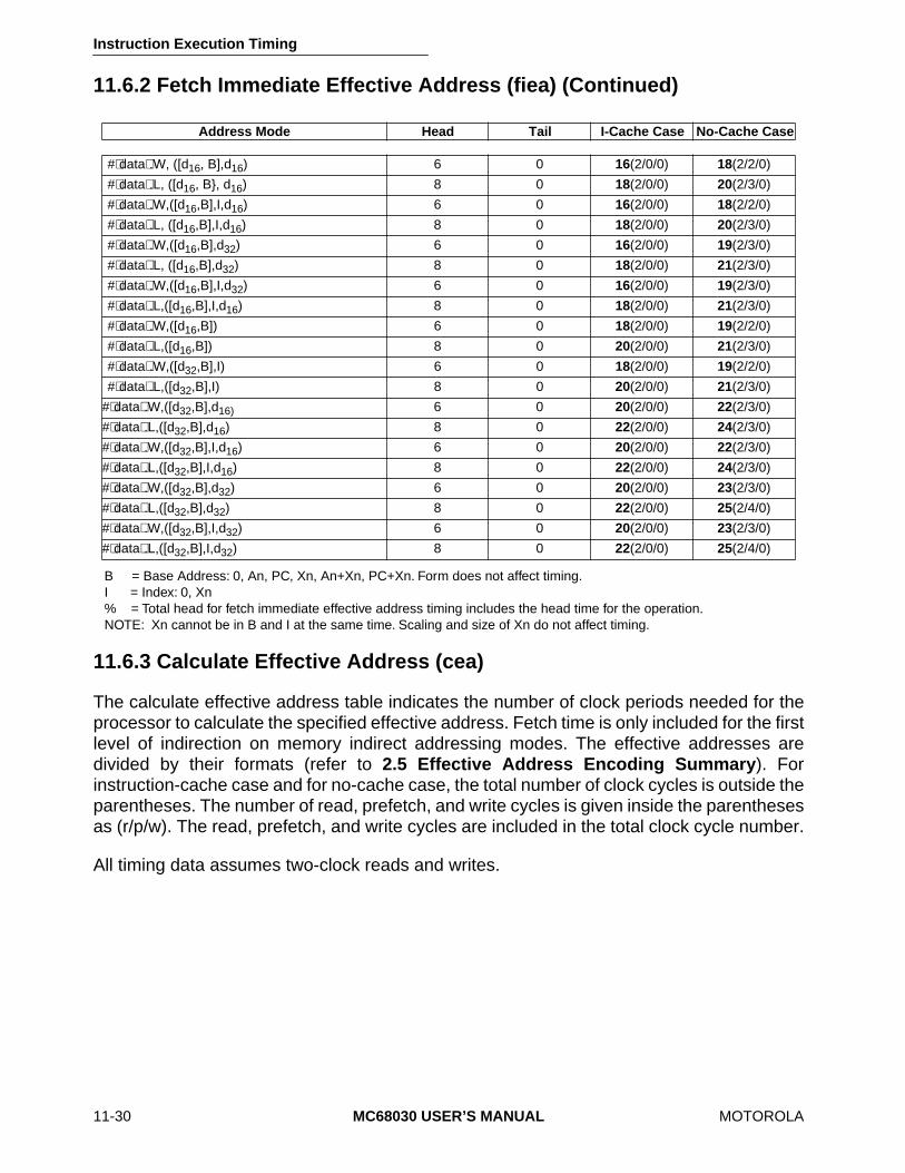
Instruction Execution Timing
11-30 MC68030 USER’S MANUAL MOTOROLA
11.6.2 Fetch Immediate Effective Address (fiea) (Continued)
B = Base Address: 0, An, PC, Xn, An+Xn, PC+Xn. Form does not affect timing.I = Index: 0, Xn% = Total head for fetch immediate effective address timing includes the head time for the operation.NOTE: Xn cannot be in B and I at the same time. Scaling and size of Xn do not affect timing.
11.6.3 Calculate Effective Address (cea)
The calculate effective address table indicates the number of clock periods needed for theprocessor to calculate the specified effective address. Fetch time is only included for the firstlevel of indirection on memory indirect addressing modes. The effective addresses aredivided by their formats (refer to 2.5 Effective Address Encoding Summary). Forinstruction-cache case and for no-cache case, the total number of clock cycles is outside theparentheses. The number of read, prefetch, and write cycles is given inside the parenthesesas (r/p/w). The read, prefetch, and write cycles are included in the total clock cycle number.
All timing data assumes two-clock reads and writes.
Address Mode Head Tail I-Cache Case No-Cache Case
#⟨data⟩.W, ([d16, B],d16) 6 0 16(2/0/0) 18(2/2/0)
#⟨data⟩.L, ([d16, B}, d16) 8 0 18(2/0/0) 20(2/3/0)
#⟨data⟩.W,([d16,B],I,d16) 6 0 16(2/0/0) 18(2/2/0)
#⟨data⟩.L, ([d16,B],I,d16) 8 0 18(2/0/0) 20(2/3/0)
#⟨data⟩.W,([d16,B],d32) 6 0 16(2/0/0) 19(2/3/0)
#⟨data⟩.L, ([d16,B],d32) 8 0 18(2/0/0) 21(2/3/0)
#⟨data⟩.W,([d16,B],I,d32) 6 0 16(2/0/0) 19(2/3/0)
#⟨data⟩.L,([d16,B],I,d16) 8 0 18(2/0/0) 21(2/3/0)
#⟨data⟩.W,([d16,B]) 6 0 18(2/0/0) 19(2/2/0)
#⟨data⟩.L,([d16,B]) 8 0 20(2/0/0) 21(2/3/0)
#⟨data⟩.W,([d32,B],I) 6 0 18(2/0/0) 19(2/2/0)
#⟨data⟩.L,([d32,B],I) 8 0 20(2/0/0) 21(2/3/0)
#⟨data⟩.W,([d32,B],d16) 6 0 20(2/0/0) 22(2/3/0)
#⟨data⟩.L,([d32,B],d16) 8 0 22(2/0/0) 24(2/3/0)
#⟨data⟩.W,([d32,B],I,d16) 6 0 20(2/0/0) 22(2/3/0)
#⟨data⟩.L,([d32,B],I,d16) 8 0 22(2/0/0) 24(2/3/0)
#⟨data⟩.W,([d32,B],d32) 6 0 20(2/0/0) 23(2/3/0)
#⟨data⟩.L,([d32,B],d32) 8 0 22(2/0/0) 25(2/4/0)
#⟨data⟩.W,([d32,B],I,d32) 6 0 20(2/0/0) 23(2/3/0)
#⟨data⟩.L,([d32,B],I,d32) 8 0 22(2/0/0) 25(2/4/0)
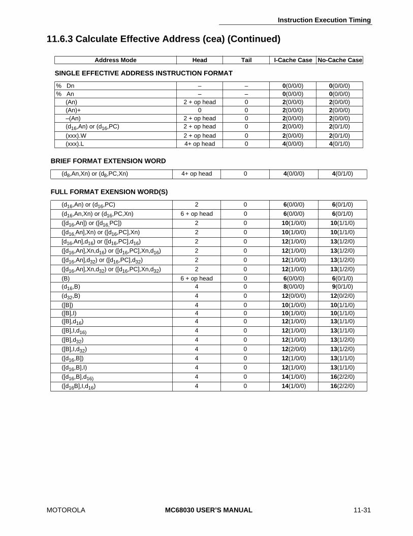
Instruction Execution Timing
MOTOROLA MC68030 USER’S MANUAL 11-31
11.6.3 Calculate Effective Address (cea) (Continued)
Address Mode Head Tail I-Cache Case No-Cache Case
SINGLE EFFECTIVE ADDRESS INSTRUCTION FORMAT
% Dn – – 0(0/0/0) 0(0/0/0)% An – – 0(0/0/0) 0(0/0/0)
(An) 2 + op head 0 2(0/0/0) 2(0/0/0)(An)+ 0 0 2(0/0/0) 2(0/0/0)–(An) 2 + op head 0 2(0/0/0) 2(0/0/0)(d16,An) or (d16,PC) 2 + op head 0 2(0/0/0) 2(0/1/0)
(xxx).W 2 + op head 0 2(0/0/0) 2(0/1/0)(xxx).L 4+ op head 0 4(0/0/0) 4(0/1/0)
BRIEF FORMAT EXTENSION WORD
(d8,An,Xn) or (d8,PC,Xn) 4+ op head 0 4(0/0/0) 4(0/1/0)
FULL FORMAT EXENSION WORD(S)
(d16,An) or (d16,PC) 2 0 6(0/0/0) 6(0/1/0)
(d16,An,Xn) or (d16,PC,Xn) 6 + op head 0 6(0/0/0) 6(0/1/0)
([d16,An]) or ([d16,PC]) 2 0 10(1/0/0) 10(1/1/0)
([d16,An],Xn) or ([d16,PC],Xn) 2 0 10(1/0/0) 10(1/1/0)
[d16,An],d16) or ([d16,PC],d16) 2 0 12(1/0/0) 13(1/2/0)
([d16,An],Xn,d16) or ([d16,PC],Xn,d16) 2 0 12(1/0/0) 13(1/2/0)
([d16,An],d32) or ([d16,PC],d32) 2 0 12(1/0/0) 13(1/2/0)
([d16,An],Xn,d32) or ([d16,PC],Xn,d32) 2 0 12(1/0/0) 13(1/2/0)
(B) 6 + op head 0 6(0/0/0) 6(0/1/0)(d16,B) 4 0 8(0/0/0) 9(0/1/0)
(d32,B) 4 0 12(0/0/0) 12(0/2/0)
([B]) 4 0 10(1/0/0) 10(1/1/0)([B],I) 4 0 10(1/0/0) 10(1/1/0)([B],d16) 4 0 12(1/0/0) 13(1/1/0)
([B],I,d16) 4 0 12(1/0/0) 13(1/1/0)
([B],d32) 4 0 12(1/0/0) 13(1/2/0)
([B],I,d32) 4 0 12(2/0/0) 13(1/2/0)
([d16,B]) 4 0 12(1/0/0) 13(1/1/0)
([d16,B],I) 4 0 12(1/0/0) 13(1/1/0)
([d16,B],d16) 4 0 14(1/0/0) 16(2/2/0)
([d16B],I,d16) 4 0 14(1/0/0) 16(2/2/0)

Instruction Execution Timing
11-32 MC68030 USER’S MANUAL MOTOROLA
11.6.3 Calculate Effective Address (cea) (Continued)
B = Base address; 0, An, PC, Xn, An+Xn, PC+Xn. Form does not affect timing.I = Index; 0, Xn% = No clock cycles incurred by effective address calculation.NOTE: Xn cannot be in B and I at the same time. Scaling and size of Xn do not affect timing.
11.6.4 Calculate Immediate Effective Address (ciea)
The calculate immediate effective address table indicates the number of clock periodsneeded for the processor to fetch the immediate source operand and calculate the specifieddestination effective address. In the case of two-word instructions, this table indicates thenumber of clock periods needed for the processor to fetch the second word of the instructionand calculate the specified source operand or single operand. Fetch time is only includedfor the first level of indirection on memory indirect addressing modes. The effectiveaddresses are divided by their formats (refer to 2.5 Effective Address EncodingSummary). For instruction-cache case and for no-cache case, the total number of clockcycles is outside the parentheses. The number of read, prefetch, and write cycles is giveninside the parentheses as (r/p/w). The read, prefetch, and write cycles are included in thetotal clock cycle number.
All timing data assumes two-clock reads and writes.
Address Mode Head Tail I-Cache Case No-Cache Case
([d16,B],d32) 4 0 14(1/0/0) 16(1/2/0)
[d16,B],I,d32) 4 0 14(1/0/0) 16(1/2/0)
[d16,B]) 4 0 16(1/0/0) 17(1/2/0)
([d16,B]I) 4 0 16(1/0/0) 17(1/2/0)
([d16,B]d16) 4 0 18(1/0/0) 20(1/2/0)
([d16,B],I,d16) 4 0 18(1/0/0) 20(1/2/0)
([d16,B],d32) 4 0 18(1/0/0) 20(1/3/0)
([d16,B],I,d32) 4 0 18(1/0/0) 20(1/3/0)
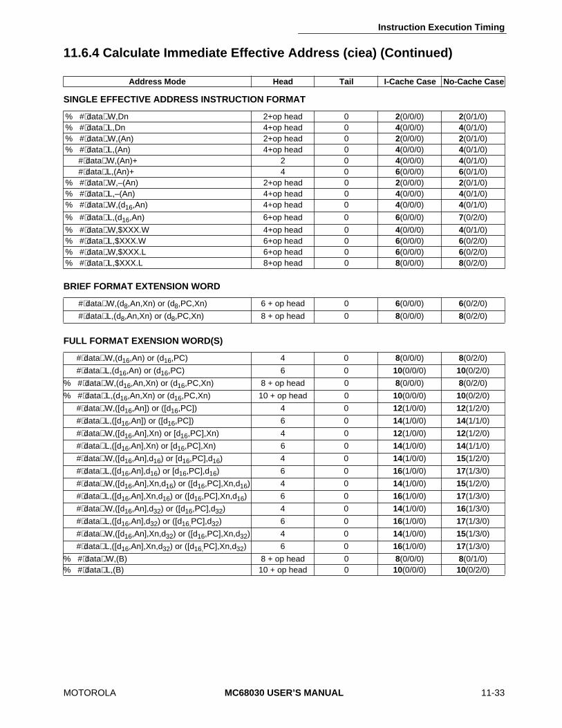
Instruction Execution Timing
MOTOROLA MC68030 USER’S MANUAL 11-33
11.6.4 Calculate Immediate Effective Address (ciea) (Continued)
Address Mode Head Tail I-Cache Case No-Cache Case
SINGLE EFFECTIVE ADDRESS INSTRUCTION FORMAT
% #⟨data⟩.W,Dn 2+op head 0 2(0/0/0) 2(0/1/0)% #⟨data⟩.L,Dn 4+op head 0 4(0/0/0) 4(0/1/0)% #⟨data⟩.W,(An) 2+op head 0 2(0/0/0) 2(0/1/0)% #⟨data⟩.L,(An) 4+op head 0 4(0/0/0) 4(0/1/0)
#⟨data⟩.W,(An)+ 2 0 4(0/0/0) 4(0/1/0)#⟨data⟩.L,(An)+ 4 0 6(0/0/0) 6(0/1/0)
% #⟨data⟩.W,–(An) 2+op head 0 2(0/0/0) 2(0/1/0)% #⟨data⟩.L,–(An) 4+op head 0 4(0/0/0) 4(0/1/0)% #⟨data⟩.W,(d16,An) 4+op head 0 4(0/0/0) 4(0/1/0)
% #⟨data⟩.L,(d16,An) 6+op head 0 6(0/0/0) 7(0/2/0)
% #⟨data⟩.W,$XXX.W 4+op head 0 4(0/0/0) 4(0/1/0)% #⟨data⟩.L,$XXX.W 6+op head 0 6(0/0/0) 6(0/2/0)% #⟨data⟩.W,$XXX.L 6+op head 0 6(0/0/0) 6(0/2/0)% #⟨data⟩.L,$XXX.L 8+op head 0 8(0/0/0) 8(0/2/0)
BRIEF FORMAT EXTENSION WORD
#⟨data⟩.W,(d8,An,Xn) or (d8,PC,Xn) 6 + op head 0 6(0/0/0) 6(0/2/0)
#⟨data⟩.L,(d8,An,Xn) or (d8,PC,Xn) 8 + op head 0 8(0/0/0) 8(0/2/0)
FULL FORMAT EXENSION WORD(S)
#⟨data⟩.W,(d16,An) or (d16,PC) 4 0 8(0/0/0) 8(0/2/0)
#⟨data⟩.L,(d16,An) or (d16,PC) 6 0 10(0/0/0) 10(0/2/0)
% #⟨data⟩.W,(d16,An,Xn) or (d16,PC,Xn) 8 + op head 0 8(0/0/0) 8(0/2/0)
% #⟨data⟩.L,(d16,An,Xn) or (d16,PC,Xn) 10 + op head 0 10(0/0/0) 10(0/2/0)
#⟨data⟩.W,([d16,An]) or ([d16,PC]) 4 0 12(1/0/0) 12(1/2/0)
#⟨data⟩.L,([d16,An]) or ([d16,PC]) 6 0 14(1/0/0) 14(1/1/0)
#⟨data⟩.W,([d16,An],Xn) or [d16,PC],Xn) 4 0 12(1/0/0) 12(1/2/0)
#⟨data⟩.L,([d16,An],Xn) or [d16,PC],Xn) 6 0 14(1/0/0) 14(1/1/0)
#⟨data⟩.W,([d16,An],d16) or [d16,PC],d16) 4 0 14(1/0/0) 15(1/2/0)
#⟨data⟩.L,([d16,An],d16) or [d16,PC],d16) 6 0 16(1/0/0) 17(1/3/0)
#⟨data⟩.W,([d16,An],Xn,d16) or ([d16,PC],Xn,d16) 4 0 14(1/0/0) 15(1/2/0)
#⟨data⟩.L,([d16,An],Xn,d16) or ([d16,PC],Xn,d16) 6 0 16(1/0/0) 17(1/3/0)
#⟨data⟩.W,([d16,An],d32) or ([d16,PC],d32) 4 0 14(1/0/0) 16(1/3/0)
#⟨data⟩.L,([d16,An],d32) or ([d16,PC],d32) 6 0 16(1/0/0) 17(1/3/0)
#⟨data⟩.W,([d16,An],Xn,d32) or ([d16,PC],Xn,d32) 4 0 14(1/0/0) 15(1/3/0)
#⟨data⟩.L,([d16,An],Xn,d32) or ([d16,PC],Xn,d32) 6 0 16(1/0/0) 17(1/3/0)
% #⟨data⟩.W,(B) 8 + op head 0 8(0/0/0) 8(0/1/0)% #⟨data⟩.L,(B) 10 + op head 0 10(0/0/0) 10(0/2/0)
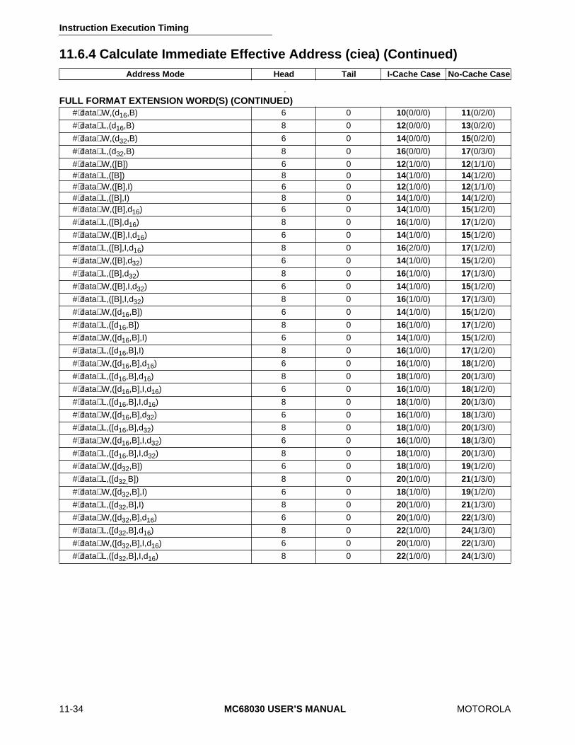
Instruction Execution Timing
11-34 MC68030 USER’S MANUAL MOTOROLA
11.6.4 Calculate Immediate Effective Address (ciea) (Continued)
.
Address Mode Head Tail I-Cache Case No-Cache Case
FULL FORMAT EXTENSION WORD(S) (CONTINUED)#⟨data⟩.W,(d16,B) 6 0 10(0/0/0) 11(0/2/0)
#⟨data⟩.L,(d16,B) 8 0 12(0/0/0) 13(0/2/0)
#⟨data⟩.W,(d32,B) 6 0 14(0/0/0) 15(0/2/0)
#⟨data⟩.L,(d32,B) 8 0 16(0/0/0) 17(0/3/0)
#⟨data⟩.W,([B]) 6 0 12(1/0/0) 12(1/1/0)#⟨data⟩.L,([B]) 8 0 14(1/0/0) 14(1/2/0)#⟨data⟩.W,([B],I) 6 0 12(1/0/0) 12(1/1/0)#⟨data⟩.L,([B],I) 8 0 14(1/0/0) 14(1/2/0)#⟨data⟩.W,([B],d16) 6 0 14(1/0/0) 15(1/2/0)
#⟨data⟩.L,([B],d16) 8 0 16(1/0/0) 17(1/2/0)
#⟨data⟩.W,([B],I,d16) 6 0 14(1/0/0) 15(1/2/0)
#⟨data⟩.L,([B],I,d16) 8 0 16(2/0/0) 17(1/2/0)
#⟨data⟩.W,([B],d32) 6 0 14(1/0/0) 15(1/2/0)
#⟨data⟩.L,([B],d32) 8 0 16(1/0/0) 17(1/3/0)
#⟨data⟩.W,([B],I,d32) 6 0 14(1/0/0) 15(1/2/0)
#⟨data⟩.L,([B],I,d32) 8 0 16(1/0/0) 17(1/3/0)
#⟨data⟩.W,([d16,B]) 6 0 14(1/0/0) 15(1/2/0)
#⟨data⟩.L,([d16,B]) 8 0 16(1/0/0) 17(1/2/0)
#⟨data⟩.W,([d16,B],I) 6 0 14(1/0/0) 15(1/2/0)
#⟨data⟩.L,([d16,B],I) 8 0 16(1/0/0) 17(1/2/0)
#⟨data⟩.W,([d16,B],d16) 6 0 16(1/0/0) 18(1/2/0)
#⟨data⟩.L,([d16,B],d16) 8 0 18(1/0/0) 20(1/3/0)
#⟨data⟩.W,([d16,B],I,d16) 6 0 16(1/0/0) 18(1/2/0)
#⟨data⟩.L,([d16,B],I,d16) 8 0 18(1/0/0) 20(1/3/0)
#⟨data⟩.W,([d16,B],d32) 6 0 16(1/0/0) 18(1/3/0)
#⟨data⟩.L,([d16,B],d32) 8 0 18(1/0/0) 20(1/3/0)
#⟨data⟩.W,([d16,B],I,d32) 6 0 16(1/0/0) 18(1/3/0)
#⟨data⟩.L,([d16,B],I,d32) 8 0 18(1/0/0) 20(1/3/0)
#⟨data⟩.W,([d32,B]) 6 0 18(1/0/0) 19(1/2/0)
#⟨data⟩.L,([d32,B]) 8 0 20(1/0/0) 21(1/3/0)
#⟨data⟩.W,([d32,B],I) 6 0 18(1/0/0) 19(1/2/0)
#⟨data⟩.L,([d32,B],I) 8 0 20(1/0/0) 21(1/3/0)
#⟨data⟩.W,([d32,B],d16) 6 0 20(1/0/0) 22(1/3/0)
#⟨data⟩.L,([d32,B],d16) 8 0 22(1/0/0) 24(1/3/0)
#⟨data⟩.W,([d32,B],I,d16) 6 0 20(1/0/0) 22(1/3/0)
#⟨data⟩.L,([d32,B],I,d16) 8 0 22(1/0/0) 24(1/3/0)
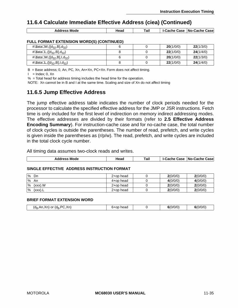
Instruction Execution Timing
MOTOROLA MC68030 USER’S MANUAL 11-35
11.6.4 Calculate Immediate Effective Address (ciea) (Continued)
B = Base address; 0, An, PC, Xn, An+Xn, PC+Xn. Form does not affect timing.I = Index; 0, Xn% = Total head for address timing includes the head time for the operation.NOTE: Xn cannot be in B and I at the same time. Scaling and size of Xn do not affect timing
11.6.5 Jump Effective Address
The jump effective address table indicates the number of clock periods needed for theprocessor to calculate the specified effective address for the JMP or JSR instructions. Fetchtime is only included for the first level of indirection on memory indirect addressing modes.The effective addresses are divided by their formats (refer to 2.5 Effective AddressEncoding Summary). For instruction-cache case and for no-cache case, the total numberof clock cycles is outside the parentheses. The number of read, prefetch, and write cyclesis given inside the parentheses as (r/p/w). The read, prefetch, and write cycles are includedin the total clock cycle number.
All timing data assumes two-clock reads and writes.
Address Mode Head Tail I-Cache Case No-Cache Case
FULL FORMAT EXTENSION WORD(S) (CONTINUED)#⟨data⟩.W,([d32,B],d32) 6 0 20(1/0/0) 22(1/3/0)
#⟨data⟩.L,([d32,B],d32) 8 0 22(1/0/0) 24(1/4/0)
#⟨data⟩.W,([d32,B],I,d32) 6 0 20(1/0/0) 22(1/3/0)
#⟨data⟩.L,([d32,B],I,d32) 8 0 22(1/0/0) 24(1/4/0)
Address Mode Head Tail I-Cache Case No-Cache Case
SINGLE EFFECTIVE ADDRESS INSTRUCTION FORMAT
% Dn 2+op head 0 2(0/0/0) 2(0/0/0)% An 4+op head 0 4(0/0/0) 4(0/0/0)% (xxx).W 2+op head 0 2(0/0/0) 2(0/0/0)% (xxx).L 2+op head 0 2(0/0/0) 2(0/0/0)
BRIEF FORMAT EXTENSION WORD
(d8,An,Xn) or (d8,PC,Xn) 6+op head 0 6(0/0/0) 6(0/0/0)
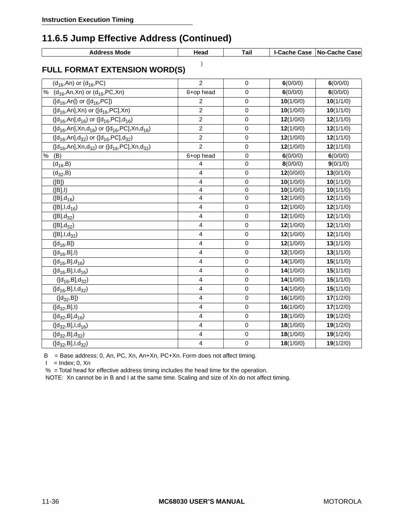
Instruction Execution Timing
11-36 MC68030 USER’S MANUAL MOTOROLA
11.6.5 Jump Effective Address (Continued)
)
B = Base address; 0, An, PC, Xn, An+Xn, PC+Xn. Form does not affect timing.I = Index; 0, Xn% = Total head for effective address timing includes the head time for the operation.NOTE: Xn cannot be in B and I at the same time. Scaling and size of Xn do not affect timing.
Address Mode Head Tail I-Cache Case No-Cache Case
FULL FORMAT EXTENSION WORD(S)
(d16,An) or (d16,PC) 2 0 6(0/0/0) 6(0/0/0)
% (d16,An,Xn) or (d16,PC,Xn) 6+op head 0 6(0/0/0) 6(0/0/0)
([d16,An]) or ([d16,PC]) 2 0 10(1/0/0) 10(1/1/0)
([d16,An],Xn) or ([d16,PC],Xn) 2 0 10(1/0/0) 10(1/1/0)
([d16,An],d16) or ([d16,PC],d16) 2 0 12(1/0/0) 12(1/1/0)
([d16,An],Xn,d16) or ([d16,PC],Xn,d16) 2 0 12(1/0/0) 12(1/1/0)
([d16,An],d32) or ([d16,PC],d32) 2 0 12(1/0/0) 12(1/1/0)
([d16,An],Xn,d32) or ([d16,PC],Xn,d32) 2 0 12(1/0/0) 12(1/1/0)
% (B) 6+op head 0 6(0/0/0) 6(0/0/0)(d16,B) 4 0 8(0/0/0) 9(0/1/0)
(d32,B) 4 0 12(0/0/0) 13(0/1/0)
([B]) 4 0 10(1/0/0) 10(1/1/0)([B],I) 4 0 10(1/0/0) 10(1/1/0)([B],d16) 4 0 12(1/0/0) 12(1/1/0)
([B],I,d16) 4 0 12(1/0/0) 12(1/1/0)
([B],d32) 4 0 12(1/0/0) 12(1/1/0)
([B],d32) 4 0 12(1/0/0) 12(1/1/0)
([B],I,d32) 4 0 12(1/0/0) 12(1/1/0)
([d16,B]) 4 0 12(1/0/0) 13(1/1/0)
([d16,B],I) 4 0 12(1/0/0) 13(1/1/0)
([d16,B],d16) 4 0 14(1/0/0) 15(1/1/0)
([d16,B],I,d16) 4 0 14(1/0/0) 15(1/1/0)
([d16,B],d32) 4 0 14(1/0/0) 15(1/1/0)
([d16,B],I,d32) 4 0 14(1/0/0) 15(1/1/0)
([d32,B]) 4 0 16(1/0/0) 17(1/2/0)
([d32,B],I) 4 0 16(1/0/0) 17(1/2/0)
([d32,B],d16) 4 0 18(1/0/0) 19(1/2/0)
([d32,B],I,d16) 4 0 18(1/0/0) 19(1/2/0)
([d32,B],d32) 4 0 18(1/0/0) 19(1/2/0)
([d32,B],I,d32) 4 0 18(1/0/0) 19(1/2/0)

Instruction Execution Timing
MOTOROLA MC68030 USER’S MANUAL 11-37
11.6.6 MOVE Instruction
The MOVE instruction timing table indicates the number of clock periods needed for theprocessor to calculate the destination effective address and perform the MOVE or MOVEAinstruction, including the first level of indirection on memory indirect addressing modes. Thefetch effective address table is needed on most MOVE operations (source, destinationdependent). The destination effective addresses are divided by their formats (refer to 2.5Effective Address Encoding Summary). For instruction-cache case and for no-cachecase, the total number of clock cycles is outside the parentheses. The number of read,prefetch, and write cycles is given inside the parentheses as (r/p/w). The read, prefetch, andwrite cycles are included in the total clock cycle number.
All timing data assumes two-clock reads and writes.MOVE Source,Destination Head Tail I-Cache Case No-Cache Case
SINGLE EFFECTIVE ADDRESS INSTRUCTION FORMATMOVE Rn, Dn 2 0 2(0/0/0) 2(0/1/0)MOVE Rn, An 2 0 2(0/0/0) 2(0/1/0)MOVE EA,An 0 0 2(0/0/0) 2(0/1/0)MOVE EA,Dn 0 0 2(0/0/0) 2(0/1/0)MOVE Rn,(An) 0 1 3(0/0/1) 4(0/1/1)MOVE SOURCE, (An) 2 0 4(0/0/1) 5(0/1/1)MOVE Rn,(An)+ 0 1 3(0/0/1) 4(0/1/1)MOVE SOURCE, (An)+ 2 0 4(0/0/1) 5(0/1/1)MOVE Rn,–(An) 0 2 4(0/0/1) 4(0/1/1)MOVE SOURCE, –(An) 2 0 4(0/0/1) 5(0/1/1)MOVE EA, (d16,An) 2 0 4(0/0/1) 5(0/1/1)
MOVE EA,XXX.W 2 0 4(0/0/1) 5(0/1/1)MOVE EA,XXX.L 0 0 6(0/0/1) 7(0/2/1)
BRIEF FORMAT EXTENSION WORDMOVE EA, (d8,An,Xn) 4 0 6(0/0/1) 7(0/1/1)
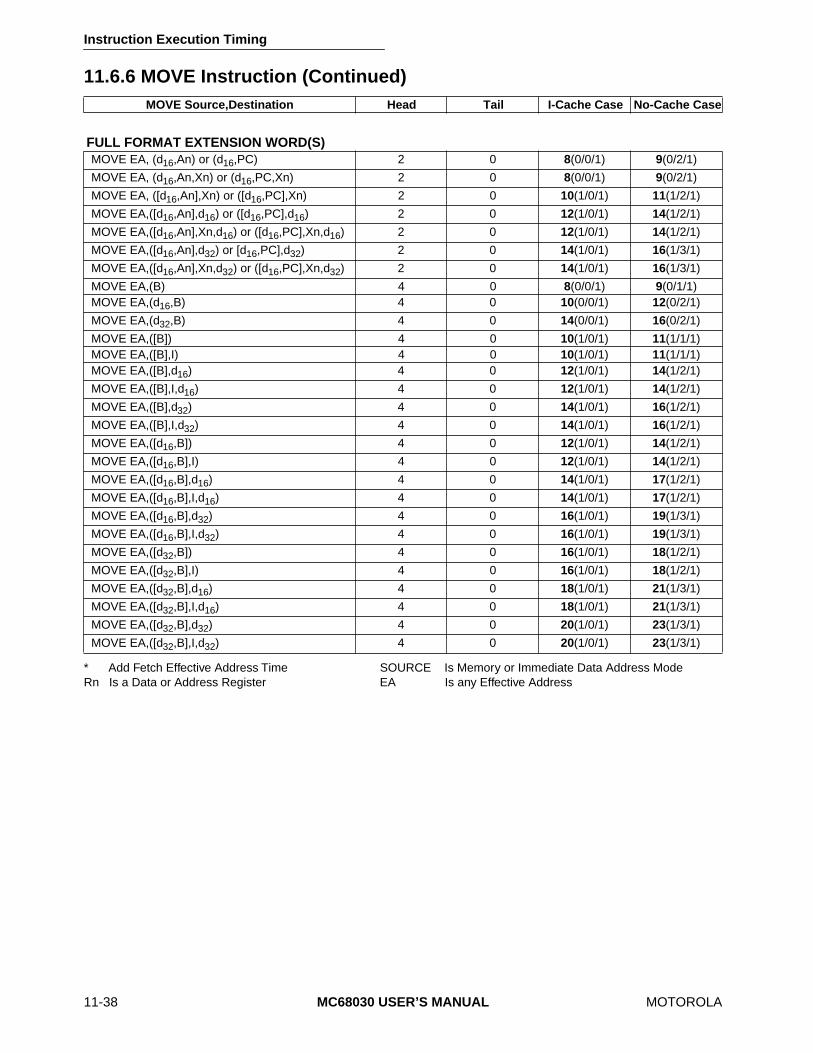
Instruction Execution Timing
11-38 MC68030 USER’S MANUAL MOTOROLA
11.6.6 MOVE Instruction (Continued)
* Add Fetch Effective Address Time SOURCE Is Memory or Immediate Data Address ModeRn Is a Data or Address Register EA Is any Effective Address
MOVE Source,Destination Head Tail I-Cache Case No-Cache Case
FULL FORMAT EXTENSION WORD(S)MOVE EA, (d16,An) or (d16,PC) 2 0 8(0/0/1) 9(0/2/1)
MOVE EA, (d16,An,Xn) or (d16,PC,Xn) 2 0 8(0/0/1) 9(0/2/1)
MOVE EA, ([d16,An],Xn) or ([d16,PC],Xn) 2 0 10(1/0/1) 11(1/2/1)
MOVE EA,([d16,An],d16) or ([d16,PC],d16) 2 0 12(1/0/1) 14(1/2/1)
MOVE EA,([d16,An],Xn,d16) or ([d16,PC],Xn,d16) 2 0 12(1/0/1) 14(1/2/1)
MOVE EA,([d16,An],d32) or [d16,PC],d32) 2 0 14(1/0/1) 16(1/3/1)
MOVE EA,([d16,An],Xn,d32) or ([d16,PC],Xn,d32) 2 0 14(1/0/1) 16(1/3/1)
MOVE EA,(B) 4 0 8(0/0/1) 9(0/1/1)MOVE EA,(d16,B) 4 0 10(0/0/1) 12(0/2/1)
MOVE EA,(d32,B) 4 0 14(0/0/1) 16(0/2/1)
MOVE EA,([B]) 4 0 10(1/0/1) 11(1/1/1)MOVE EA,([B],I) 4 0 10(1/0/1) 11(1/1/1)MOVE EA,([B],d16) 4 0 12(1/0/1) 14(1/2/1)
MOVE EA,([B],I,d16) 4 0 12(1/0/1) 14(1/2/1)
MOVE EA,([B],d32) 4 0 14(1/0/1) 16(1/2/1)
MOVE EA,([B],I,d32) 4 0 14(1/0/1) 16(1/2/1)
MOVE EA,([d16,B]) 4 0 12(1/0/1) 14(1/2/1)
MOVE EA,([d16,B],I) 4 0 12(1/0/1) 14(1/2/1)
MOVE EA,([d16,B],d16) 4 0 14(1/0/1) 17(1/2/1)
MOVE EA,([d16,B],I,d16) 4 0 14(1/0/1) 17(1/2/1)
MOVE EA,([d16,B],d32) 4 0 16(1/0/1) 19(1/3/1)
MOVE EA,([d16,B],I,d32) 4 0 16(1/0/1) 19(1/3/1)
MOVE EA,([d32,B]) 4 0 16(1/0/1) 18(1/2/1)
MOVE EA,([d32,B],I) 4 0 16(1/0/1) 18(1/2/1)
MOVE EA,([d32,B],d16) 4 0 18(1/0/1) 21(1/3/1)
MOVE EA,([d32,B],I,d16) 4 0 18(1/0/1) 21(1/3/1)
MOVE EA,([d32,B],d32) 4 0 20(1/0/1) 23(1/3/1)
MOVE EA,([d32,B],I,d32) 4 0 20(1/0/1) 23(1/3/1)
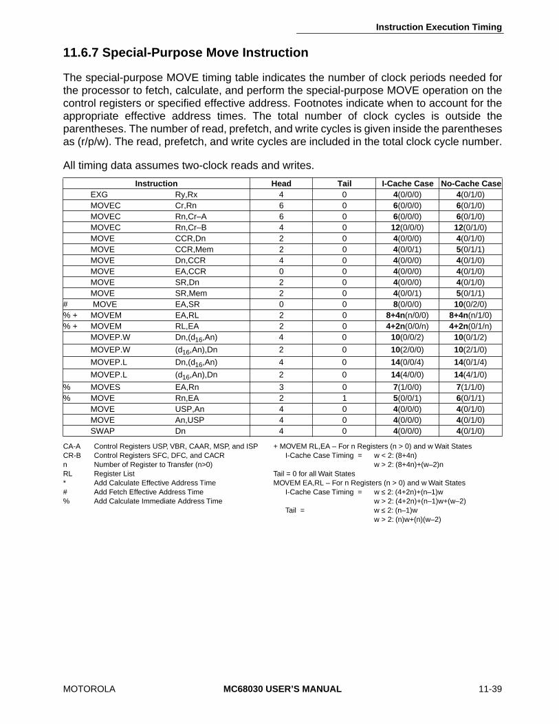
Instruction Execution Timing
MOTOROLA MC68030 USER’S MANUAL 11-39
11.6.7 Special-Purpose Move Instruction
The special-purpose MOVE timing table indicates the number of clock periods needed forthe processor to fetch, calculate, and perform the special-purpose MOVE operation on thecontrol registers or specified effective address. Footnotes indicate when to account for theappropriate effective address times. The total number of clock cycles is outside theparentheses. The number of read, prefetch, and write cycles is given inside the parenthesesas (r/p/w). The read, prefetch, and write cycles are included in the total clock cycle number.
All timing data assumes two-clock reads and writes.
CA-A Control Registers USP, VBR, CAAR, MSP, and ISP + MOVEM RL,EA – For n Registers (n > 0) and w Wait StatesCR-B Control Registers SFC, DFC, and CACR I-Cache Case Timing = w < 2: (8+4n)n Number of Register to Transfer (n>0) w > 2: (8+4n)+(w–2)nRL Register List Tail = 0 for all Wait States* Add Calculate Effective Address Time MOVEM EA,RL – For n Registers (n > 0) and w Wait States# Add Fetch Effective Address Time I-Cache Case Timing = w ≤ 2: (4+2n)+(n–1)w% Add Calculate Immediate Address Time w > 2: (4+2n)+(n–1)w+(w–2)
Tail = w ≤ 2: (n–1)ww > 2: (n)w+(n)(w–2)
Instruction Head Tail I-Cache Case No-Cache CaseEXG Ry,Rx 4 0 4(0/0/0) 4(0/1/0)MOVEC Cr,Rn 6 0 6(0/0/0) 6(0/1/0)MOVEC Rn,Cr–A 6 0 6(0/0/0) 6(0/1/0)MOVEC Rn,Cr–B 4 0 12(0/0/0) 12(0/1/0)MOVE CCR,Dn 2 0 4(0/0/0) 4(0/1/0)MOVE CCR,Mem 2 0 4(0/0/1) 5(0/1/1)MOVE Dn,CCR 4 0 4(0/0/0) 4(0/1/0)MOVE EA,CCR 0 0 4(0/0/0) 4(0/1/0)MOVE SR,Dn 2 0 4(0/0/0) 4(0/1/0)MOVE SR,Mem 2 0 4(0/0/1) 5(0/1/1)
# MOVE EA,SR 0 0 8(0/0/0) 10(0/2/0)% + MOVEM EA,RL 2 0 8+4n(n/0/0) 8+4n(n/1/0)% + MOVEM RL,EA 2 0 4+2n(0/0/n) 4+2n(0/1/n)
MOVEP.W Dn,(d16,An) 4 0 10(0/0/2) 10(0/1/2)
MOVEP.W (d16,An),Dn 2 0 10(2/0/0) 10(2/1/0)
MOVEP.L Dn,(d16,An) 4 0 14(0/0/4) 14(0/1/4)
MOVEP.L (d16,An),Dn 2 0 14(4/0/0) 14(4/1/0)
% MOVES EA,Rn 3 0 7(1/0/0) 7(1/1/0)% MOVE Rn,EA 2 1 5(0/0/1) 6(0/1/1)
MOVE USP,An 4 0 4(0/0/0) 4(0/1/0)MOVE An,USP 4 0 4(0/0/0) 4(0/1/0)SWAP Dn 4 0 4(0/0/0) 4(0/1/0)
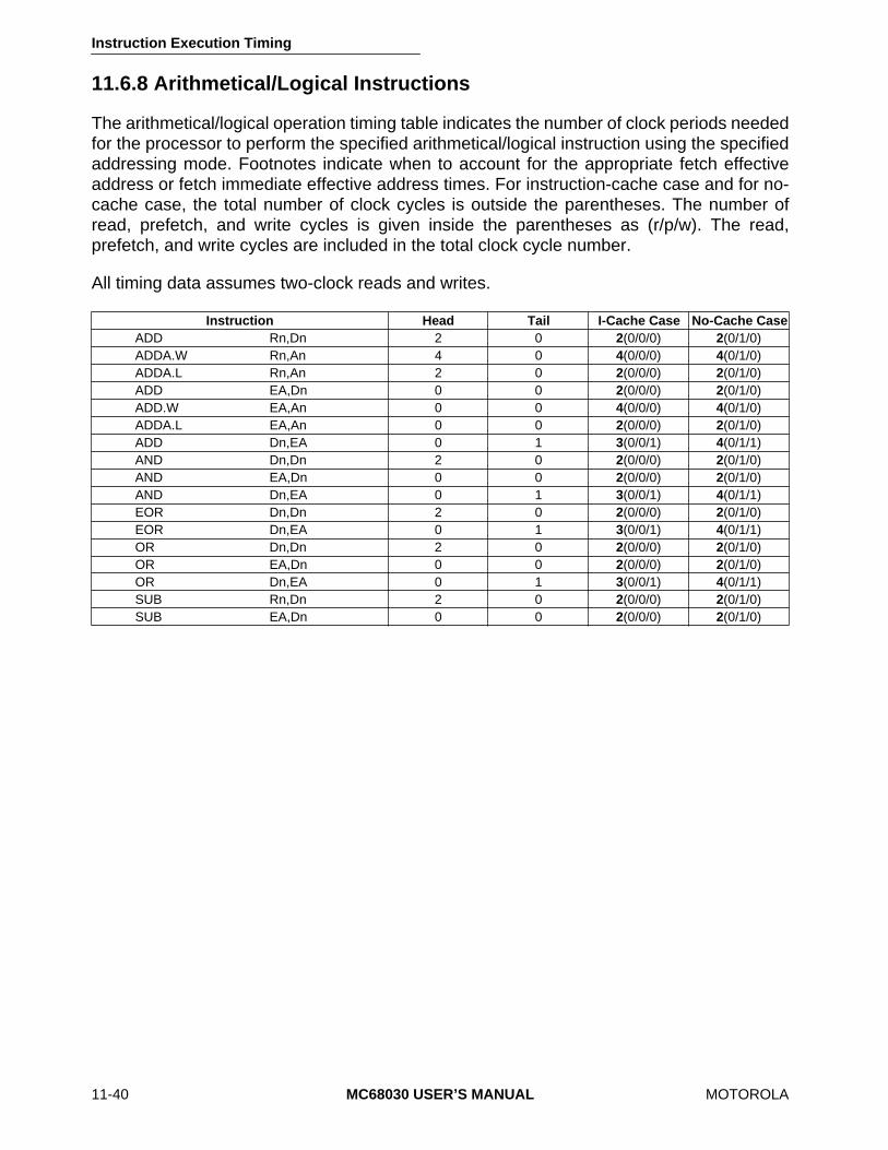
Instruction Execution Timing
11-40 MC68030 USER’S MANUAL MOTOROLA
11.6.8 Arithmetical/Logical Instructions
The arithmetical/logical operation timing table indicates the number of clock periods neededfor the processor to perform the specified arithmetical/logical instruction using the specifiedaddressing mode. Footnotes indicate when to account for the appropriate fetch effectiveaddress or fetch immediate effective address times. For instruction-cache case and for no-cache case, the total number of clock cycles is outside the parentheses. The number ofread, prefetch, and write cycles is given inside the parentheses as (r/p/w). The read,prefetch, and write cycles are included in the total clock cycle number.
All timing data assumes two-clock reads and writes.
Instruction Head Tail I-Cache Case No-Cache CaseADD Rn,Dn 2 0 2(0/0/0) 2(0/1/0)ADDA.W Rn,An 4 0 4(0/0/0) 4(0/1/0)ADDA.L Rn,An 2 0 2(0/0/0) 2(0/1/0)ADD EA,Dn 0 0 2(0/0/0) 2(0/1/0)ADD.W EA,An 0 0 4(0/0/0) 4(0/1/0)ADDA.L EA,An 0 0 2(0/0/0) 2(0/1/0)ADD Dn,EA 0 1 3(0/0/1) 4(0/1/1)AND Dn,Dn 2 0 2(0/0/0) 2(0/1/0)AND EA,Dn 0 0 2(0/0/0) 2(0/1/0)AND Dn,EA 0 1 3(0/0/1) 4(0/1/1)EOR Dn,Dn 2 0 2(0/0/0) 2(0/1/0)EOR Dn,EA 0 1 3(0/0/1) 4(0/1/1)OR Dn,Dn 2 0 2(0/0/0) 2(0/1/0)OR EA,Dn 0 0 2(0/0/0) 2(0/1/0)OR Dn,EA 0 1 3(0/0/1) 4(0/1/1)SUB Rn,Dn 2 0 2(0/0/0) 2(0/1/0)SUB EA,Dn 0 0 2(0/0/0) 2(0/1/0)
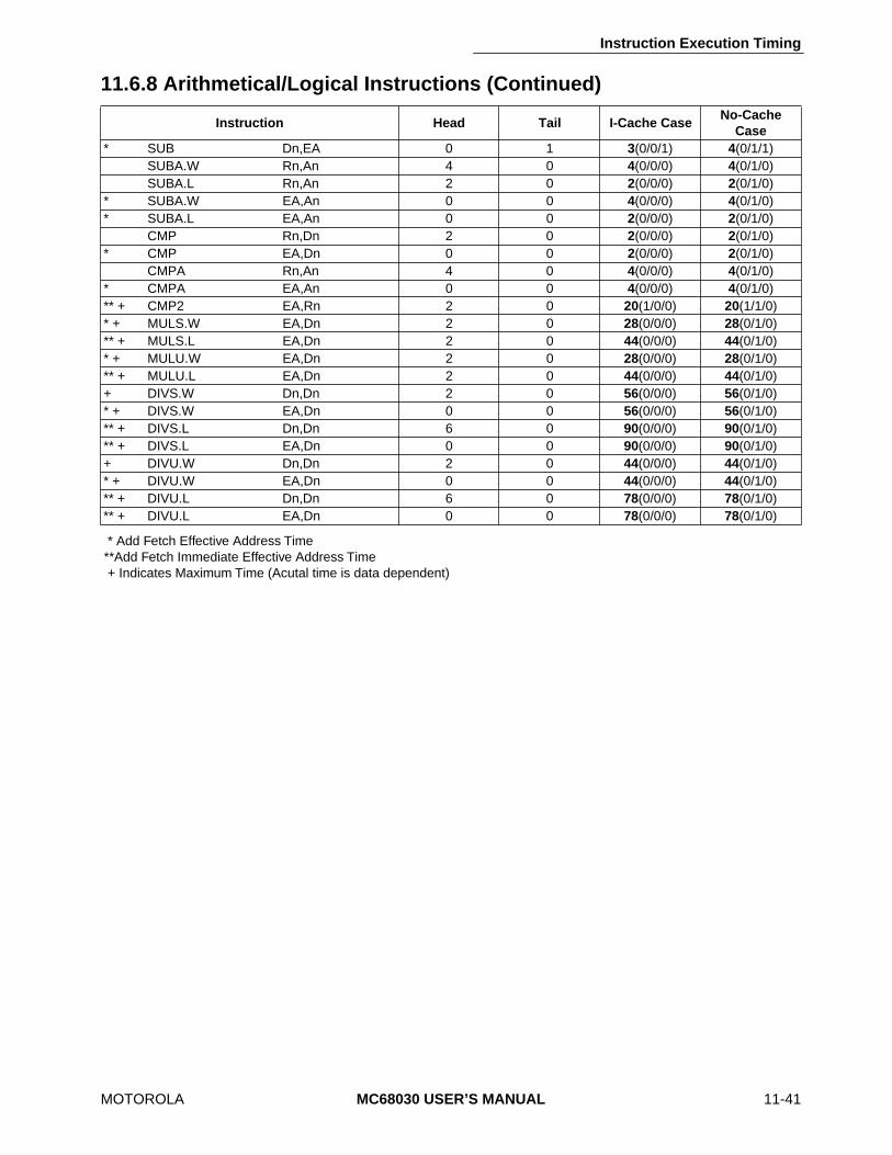
Instruction Execution Timing
MOTOROLA MC68030 USER’S MANUAL 11-41
11.6.8 Arithmetical/Logical Instructions (Continued)
* Add Fetch Effective Address Time**Add Fetch Immediate Effective Address Time + Indicates Maximum Time (Acutal time is data dependent)
Instruction Head Tail I-Cache CaseNo-Cache
Case* SUB Dn,EA 0 1 3(0/0/1) 4(0/1/1)
SUBA.W Rn,An 4 0 4(0/0/0) 4(0/1/0)SUBA.L Rn,An 2 0 2(0/0/0) 2(0/1/0)
* SUBA.W EA,An 0 0 4(0/0/0) 4(0/1/0)* SUBA.L EA,An 0 0 2(0/0/0) 2(0/1/0)
CMP Rn,Dn 2 0 2(0/0/0) 2(0/1/0)* CMP EA,Dn 0 0 2(0/0/0) 2(0/1/0)
CMPA Rn,An 4 0 4(0/0/0) 4(0/1/0)* CMPA EA,An 0 0 4(0/0/0) 4(0/1/0)** + CMP2 EA,Rn 2 0 20(1/0/0) 20(1/1/0)* + MULS.W EA,Dn 2 0 28(0/0/0) 28(0/1/0)** + MULS.L EA,Dn 2 0 44(0/0/0) 44(0/1/0)* + MULU.W EA,Dn 2 0 28(0/0/0) 28(0/1/0)** + MULU.L EA,Dn 2 0 44(0/0/0) 44(0/1/0)+ DIVS.W Dn,Dn 2 0 56(0/0/0) 56(0/1/0)* + DIVS.W EA,Dn 0 0 56(0/0/0) 56(0/1/0)** + DIVS.L Dn,Dn 6 0 90(0/0/0) 90(0/1/0)** + DIVS.L EA,Dn 0 0 90(0/0/0) 90(0/1/0)+ DIVU.W Dn,Dn 2 0 44(0/0/0) 44(0/1/0)* + DIVU.W EA,Dn 0 0 44(0/0/0) 44(0/1/0)** + DIVU.L Dn,Dn 6 0 78(0/0/0) 78(0/1/0)** + DIVU.L EA,Dn 0 0 78(0/0/0) 78(0/1/0)

Instruction Execution Timing
11-42 MC68030 USER’S MANUAL MOTOROLA
11.6.9 Immediate Arithmetical/Logical Instructions
The immediate arithmetical/logical operation timing table indicates the number of clockperiods needed for the processor to fetch the source immediate data value and to performthe specified arithmetic/logical operation using the specified destination addressing mode.Footnotes indicate when to account for the appropriate fetch effective or fetch immediateeffective address times. For instruction-cache case and for no-cache case, the total numberof clock cycles is outside the parentheses. The number of read, prefetch, and write cyclesis given inside the parentheses as (r/p/w). The read, prefetch, and write cycles are includedin the total clock cycle number.
All timing data assumes two-clock reads and writes.
* Add Fetch Effective Address Time**Add Fetch Immediate Effective Address Time
Instruction Head Tail I-Cache CaseNo-Cache
CaseMOVEQ #⟨data⟩,Dn 2 0 2(0/0/0) 2(0/1/0)ADDQ #⟨data⟩,Rn 2 0 2(0/0/0) 2(0/1/0)ADDQ #⟨data⟩,Mem 0 1 3(0/0/1) 4(0/1/1)SUBQ #⟨data⟩,Rn 2 0 2(0/0/0) 2(0/1/0)SUBQ #⟨data⟩,Mem 0 1 3(0/0/1) 4(0/1/1)ADDI #⟨data⟩,Dn 2 0 2(0/0/0) 2(0/1/0)ADDI #⟨data⟩,Mem 0 1 3(0/0/1) 4(0/1/1)ANDI #⟨data⟩,Dn 2 0 2(0/0/0) 2(0/1/0)ANDI #⟨data⟩,Mem 0 1 3(0/0/1) 4(0/1/1)EORI #⟨data⟩,Dn 2 0 2(0/0/0) 2(0/1/0)EORI #⟨data⟩,Mem 0 1 3(0/0/1) 4(0/1/1)ORI #⟨data⟩,Dn 2 0 2(0/0/0) 2(0/1/0)ORI #⟨data⟩,Mem 0 1 3(0/0/1) 4(0/1/1)SUBI #⟨data⟩,Dn 2 0 2(0/0/0) 2(0/1/0)SUBI #⟨data⟩,Mem 0 1 3(0/0/1) 4(0/1/1)CMPI #⟨data⟩,Dn 2 0 2(0/0/0) 2(0/1/0)CMPI #⟨data⟩,Mem 0 0 2(0/0/0) 2(0/1/0)
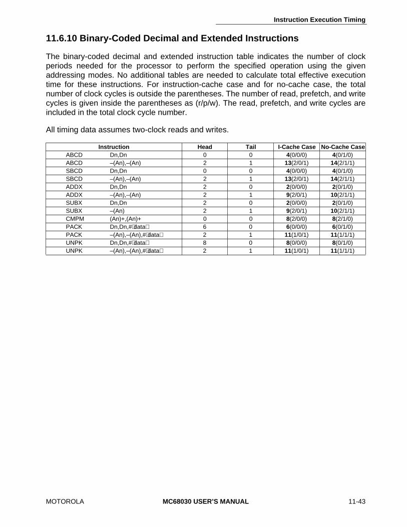
Instruction Execution Timing
MOTOROLA MC68030 USER’S MANUAL 11-43
11.6.10 Binary-Coded Decimal and Extended Instructions
The binary-coded decimal and extended instruction table indicates the number of clockperiods needed for the processor to perform the specified operation using the givenaddressing modes. No additional tables are needed to calculate total effective executiontime for these instructions. For instruction-cache case and for no-cache case, the totalnumber of clock cycles is outside the parentheses. The number of read, prefetch, and writecycles is given inside the parentheses as (r/p/w). The read, prefetch, and write cycles areincluded in the total clock cycle number.
All timing data assumes two-clock reads and writes.
Instruction Head Tail I-Cache Case No-Cache CaseABCD Dn,Dn 0 0 4(0/0/0) 4(0/1/0)ABCD –(An),–(An) 2 1 13(2/0/1) 14(2/1/1)SBCD Dn,Dn 0 0 4(0/0/0) 4(0/1/0)SBCD –(An),–(An) 2 1 13(2/0/1) 14(2/1/1)ADDX Dn,Dn 2 0 2(0/0/0) 2(0/1/0)ADDX –(An),–(An) 2 1 9(2/0/1) 10(2/1/1)SUBX Dn,Dn 2 0 2(0/0/0) 2(0/1/0)SUBX –(An) 2 1 9(2/0/1) 10(2/1/1)CMPM (An)+,(An)+ 0 0 8(2/0/0) 8(2/1/0)PACK Dn,Dn,#⟨data⟩ 6 0 6(0/0/0) 6(0/1/0)PACK –(An),–(An),#⟨data⟩ 2 1 11(1/0/1) 11(1/1/1)UNPK Dn,Dn,#⟨data⟩ 8 0 8(0/0/0) 8(0/1/0)UNPK –(An),–(An),#⟨data⟩ 2 1 11(1/0/1) 11(1/1/1)
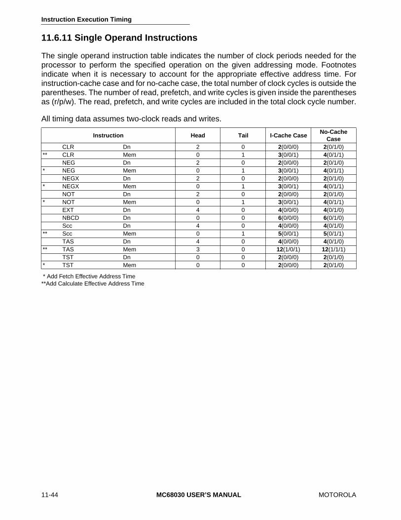
Instruction Execution Timing
11-44 MC68030 USER’S MANUAL MOTOROLA
11.6.11 Single Operand Instructions
The single operand instruction table indicates the number of clock periods needed for theprocessor to perform the specified operation on the given addressing mode. Footnotesindicate when it is necessary to account for the appropriate effective address time. Forinstruction-cache case and for no-cache case, the total number of clock cycles is outside theparentheses. The number of read, prefetch, and write cycles is given inside the parenthesesas (r/p/w). The read, prefetch, and write cycles are included in the total clock cycle number.
All timing data assumes two-clock reads and writes.
* Add Fetch Effective Address Time**Add Calculate Effective Address Time
Instruction Head Tail I-Cache CaseNo-Cache
CaseCLR Dn 2 0 2(0/0/0) 2(0/1/0)
** CLR Mem 0 1 3(0/0/1) 4(0/1/1)NEG Dn 2 0 2(0/0/0) 2(0/1/0)
* NEG Mem 0 1 3(0/0/1) 4(0/1/1)NEGX Dn 2 0 2(0/0/0) 2(0/1/0)
* NEGX Mem 0 1 3(0/0/1) 4(0/1/1)NOT Dn 2 0 2(0/0/0) 2(0/1/0)
* NOT Mem 0 1 3(0/0/1) 4(0/1/1)EXT Dn 4 0 4(0/0/0) 4(0/1/0)NBCD Dn 0 0 6(0/0/0) 6(0/1/0)Scc Dn 4 0 4(0/0/0) 4(0/1/0)
** Scc Mem 0 1 5(0/0/1) 5(0/1/1)TAS Dn 4 0 4(0/0/0) 4(0/1/0)
** TAS Mem 3 0 12(1/0/1) 12(1/1/1)TST Dn 0 0 2(0/0/0) 2(0/1/0)
* TST Mem 0 0 2(0/0/0) 2(0/1/0)

Instruction Execution Timing
MOTOROLA MC68030 USER’S MANUAL 11-45
11.6.12 Shift/Rotate Instructions
The shift/rotate instruction table indicates the number of clock periods needed for theprocessor to perform the specified operation on the given addressing mode. Footnotesindicate when it is necessary to account for the appropriate effective address time. Thenumber of bits shifted does not affect the execution time, unless noted. For instruction-cachecase and for no-cache case, the total number of clock cycles is outside the parentheses. Thenumber of read, prefetch, and write cycles is given inside the parentheses as (r/p/w). Theread, prefetch, and write cycles are included in the total clock cycle number.
All timing data assumes two-clock reads and writes.
d Direction of shift/rotate: L or R* Add Fetch Effective Address Time% Indicates shift count is less than or equal to the size of data+ Indicates shift count is greater than size of data
Instruction Head Tail I-Cache CaseNo-Cache
CaseLSd #⟨data⟩,Dy 4 0 4(0/0/0) 4(0/1/0)
% LSd Dx,Dy 6 0 6(0/0/0) 6(0/1/0)+ LSd Dx,Dy 8 0 8(0/0/0) 8(0/1/0)* LSd Mem by 1 0 0 4(0/0/1) 4(0/1/1)
ASL #⟨data⟩,Dy 2 0 6(0/0/0) 6(0/1/0)ASL Dx,Dy 4 0 8(0/0/0) 8(0/1/0)
* ASL Mem by 1 0 0 6(0/0/1) 6(0/1/1)ASR #⟨data⟩,Dy 4 0 4(0/0/0) 4(0/1/0)
% ASR Dx,Dy 6 0 6(0/0/0) 6(0/1/0)+ ASR Dx,Dy 10 0 10(0/0/0) 10(0/1/0)* ASR Mem by 1 0 0 4(0/0/1) 4(0/1/1)
ROd #⟨data⟩,Dy 4 0 6(0/0/0) 6(0/1/0)ROd Dx,Dy 6 0 8(0/0/0) 8(0/1/0)
* ROd Mem by 1 0 0 6(0/0/1) 6(0/1/1)ROXd Dn 10 0 12(0/0/0) 12(0/1/0)
* ROXd Mem by 1 0 0 4(0/0/0) 4(0/1/0)

Instruction Execution Timing
11-46 MC68030 USER’S MANUAL MOTOROLA
11.6.13 Bit Manipulation Instructions
The bit manipulation instruction table indicates the number of clock periods needed for theprocessor to perform the specified bit operation on the given addressing mode. Footnotesindicate when it is necessary to account for the appropriate effective address time. Forinstruction-cache case and for no-cache case, the total number of clock cycles is outside theparentheses. The number of read, prefetch, and write cycles is given inside the parenthesesas (r/p/w). The read, prefetch, and write cycles are included in the total clock cycle number.
All timing data assumes two-clock reads and writes.
* Add Fetch Effective Address Time# Add Fetch Immediate Effective Address Time
Instruction Head Tail I-Cache Case No-Cache CaseBTST #⟨data⟩,Dn 4 0 4(0/0/0) 4(0/1/0)BTST Dn,Dn 4 0 4(0/0/0) 4(0/1/0)
# BTST #⟨data⟩,Mem 0 0 4(0/0/0) 4(0/1/0)* BTST Dn,Mem 0 0 4(0/0/0) 4(0/1/0)
BCHG #⟨data⟩,Dn 6 0 6(0/0/0) 6(0/1/0)BCHG Dn,Dn 6 0 6(0/0/0) 6(0/1/0)
# BCHG #⟨data⟩,Mem 0 0 6(0/0/1) 6(0/1/1)* BCHG Dn,Mem 0 0 6(0/0/1) 6(0/1/1)
BCLR #⟨data⟩,Dn 6 0 6(0/0/0) 6(0/1/0)BCLR Dn,Dn 6 0 6(0/0/0) 6(0/1/0)
# BCLR #⟨data⟩,Mem 0 0 6(0/0/1) 6(0/1/1)* BCLR Dn,Mem 0 0 6(0/0/1) 6(0/1/1)
BSET #⟨data⟩,Dn 6 0 6(0/0/0) 6(0/1/0)BSET Dn,Dn 6 0 6(0/0/0) 6(0/1/0)
# BSET #⟨data⟩,Mem 0 0 6(0/0/1) 6(0/1/1)* BSET Dn,Mem 0 0 6(0/0/1) 6(0/1/1)
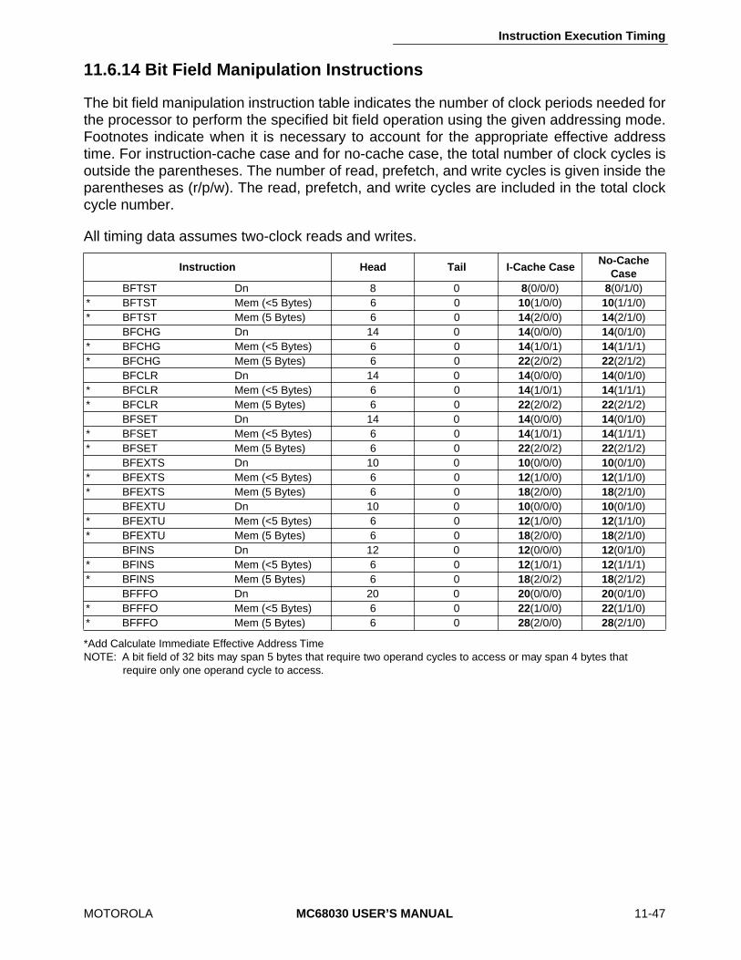
Instruction Execution Timing
MOTOROLA MC68030 USER’S MANUAL 11-47
11.6.14 Bit Field Manipulation Instructions
The bit field manipulation instruction table indicates the number of clock periods needed forthe processor to perform the specified bit field operation using the given addressing mode.Footnotes indicate when it is necessary to account for the appropriate effective addresstime. For instruction-cache case and for no-cache case, the total number of clock cycles isoutside the parentheses. The number of read, prefetch, and write cycles is given inside theparentheses as (r/p/w). The read, prefetch, and write cycles are included in the total clockcycle number.
All timing data assumes two-clock reads and writes.
*Add Calculate Immediate Effective Address TimeNOTE: A bit field of 32 bits may span 5 bytes that require two operand cycles to access or may span 4 bytes that
require only one operand cycle to access.
Instruction Head Tail I-Cache CaseNo-Cache
CaseBFTST Dn 8 0 8(0/0/0) 8(0/1/0)
* BFTST Mem (<5 Bytes) 6 0 10(1/0/0) 10(1/1/0)* BFTST Mem (5 Bytes) 6 0 14(2/0/0) 14(2/1/0)
BFCHG Dn 14 0 14(0/0/0) 14(0/1/0)* BFCHG Mem (<5 Bytes) 6 0 14(1/0/1) 14(1/1/1)* BFCHG Mem (5 Bytes) 6 0 22(2/0/2) 22(2/1/2)
BFCLR Dn 14 0 14(0/0/0) 14(0/1/0)* BFCLR Mem (<5 Bytes) 6 0 14(1/0/1) 14(1/1/1)* BFCLR Mem (5 Bytes) 6 0 22(2/0/2) 22(2/1/2)
BFSET Dn 14 0 14(0/0/0) 14(0/1/0)* BFSET Mem (<5 Bytes) 6 0 14(1/0/1) 14(1/1/1)* BFSET Mem (5 Bytes) 6 0 22(2/0/2) 22(2/1/2)
BFEXTS Dn 10 0 10(0/0/0) 10(0/1/0)* BFEXTS Mem (<5 Bytes) 6 0 12(1/0/0) 12(1/1/0)* BFEXTS Mem (5 Bytes) 6 0 18(2/0/0) 18(2/1/0)
BFEXTU Dn 10 0 10(0/0/0) 10(0/1/0)* BFEXTU Mem (<5 Bytes) 6 0 12(1/0/0) 12(1/1/0)* BFEXTU Mem (5 Bytes) 6 0 18(2/0/0) 18(2/1/0)
BFINS Dn 12 0 12(0/0/0) 12(0/1/0)* BFINS Mem (<5 Bytes) 6 0 12(1/0/1) 12(1/1/1)* BFINS Mem (5 Bytes) 6 0 18(2/0/2) 18(2/1/2)
BFFFO Dn 20 0 20(0/0/0) 20(0/1/0)* BFFFO Mem (<5 Bytes) 6 0 22(1/0/0) 22(1/1/0)* BFFFO Mem (5 Bytes) 6 0 28(2/0/0) 28(2/1/0)
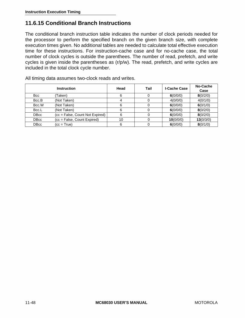
Instruction Execution Timing
11-48 MC68030 USER’S MANUAL MOTOROLA
11.6.15 Conditional Branch Instructions
The conditional branch instruction table indicates the number of clock periods needed forthe processor to perform the specified branch on the given branch size, with completeexecution times given. No additional tables are needed to calculate total effective executiontime for these instructions. For instruction-cache case and for no-cache case, the totalnumber of clock cycles is outside the parenthees. The number of read, prefetch, and writecycles is given inside the parentheses as (r/p/w). The read, prefetch, and write cycles areincluded in the total clock cycle number.
All timing data assumes two-clock reads and writes.
Instruction Head Tail I-Cache CaseNo-Cache
CaseBcc (Taken) 6 0 6(0/0/0) 8(0/2/0)Bcc.B (Not Taken) 4 0 4(0/0/0) 4(0/1/0)Bcc.W (Not Taken) 6 0 6(0/0/0) 6(0/1/0)Bcc.L (Not Taken) 6 0 6(0/0/0) 8(0/2/0)DBcc (cc = False, Count Not Expired) 6 0 6(0/0/0) 8(0/2/0)DBcc (cc = False, Count Expired) 10 0 10(0/0/0) 13(0/3/0)DBcc (cc = True) 6 0 6(0/0/0) 8(0/1/0)
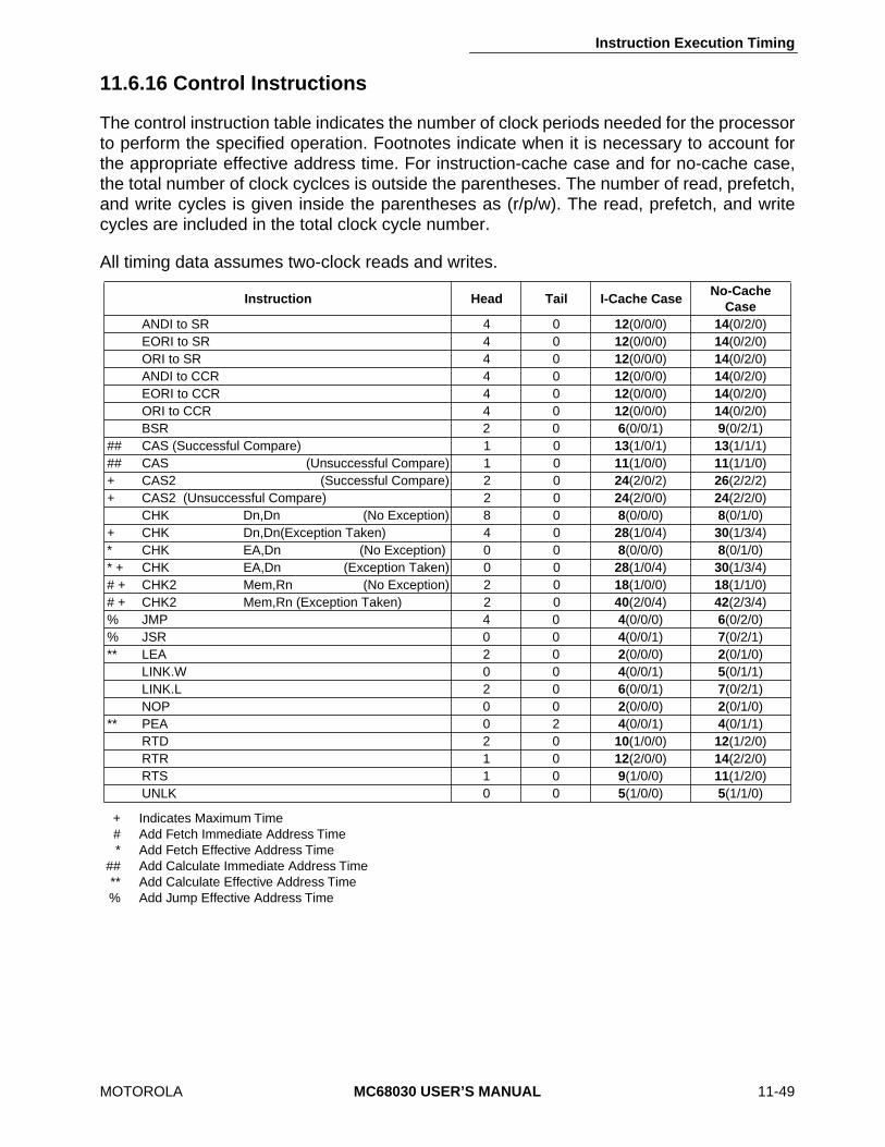
Instruction Execution Timing
MOTOROLA MC68030 USER’S MANUAL 11-49
11.6.16 Control Instructions
The control instruction table indicates the number of clock periods needed for the processorto perform the specified operation. Footnotes indicate when it is necessary to account forthe appropriate effective address time. For instruction-cache case and for no-cache case,the total number of clock cyclces is outside the parentheses. The number of read, prefetch,and write cycles is given inside the parentheses as (r/p/w). The read, prefetch, and writecycles are included in the total clock cycle number.
All timing data assumes two-clock reads and writes.
+ Indicates Maximum Time# Add Fetch Immediate Address Time* Add Fetch Effective Address Time
## Add Calculate Immediate Address Time** Add Calculate Effective Address Time% Add Jump Effective Address Time
Instruction Head Tail I-Cache CaseNo-Cache
CaseANDI to SR 4 0 12(0/0/0) 14(0/2/0)EORI to SR 4 0 12(0/0/0) 14(0/2/0)ORI to SR 4 0 12(0/0/0) 14(0/2/0)ANDI to CCR 4 0 12(0/0/0) 14(0/2/0)EORI to CCR 4 0 12(0/0/0) 14(0/2/0)ORI to CCR 4 0 12(0/0/0) 14(0/2/0)BSR 2 0 6(0/0/1) 9(0/2/1)
## CAS (Successful Compare) 1 0 13(1/0/1) 13(1/1/1)## CAS (Unsuccessful Compare) 1 0 11(1/0/0) 11(1/1/0)+ CAS2 (Successful Compare) 2 0 24(2/0/2) 26(2/2/2)+ CAS2 (Unsuccessful Compare) 2 0 24(2/0/0) 24(2/2/0)
CHK Dn,Dn (No Exception) 8 0 8(0/0/0) 8(0/1/0)+ CHK Dn,Dn(Exception Taken) 4 0 28(1/0/4) 30(1/3/4)* CHK EA,Dn (No Exception) 0 0 8(0/0/0) 8(0/1/0)* + CHK EA,Dn (Exception Taken) 0 0 28(1/0/4) 30(1/3/4)# + CHK2 Mem,Rn (No Exception) 2 0 18(1/0/0) 18(1/1/0)# + CHK2 Mem,Rn (Exception Taken) 2 0 40(2/0/4) 42(2/3/4)% JMP 4 0 4(0/0/0) 6(0/2/0)% JSR 0 0 4(0/0/1) 7(0/2/1)** LEA 2 0 2(0/0/0) 2(0/1/0)
LINK.W 0 0 4(0/0/1) 5(0/1/1)LINK.L 2 0 6(0/0/1) 7(0/2/1)NOP 0 0 2(0/0/0) 2(0/1/0)
** PEA 0 2 4(0/0/1) 4(0/1/1)RTD 2 0 10(1/0/0) 12(1/2/0)RTR 1 0 12(2/0/0) 14(2/2/0)RTS 1 0 9(1/0/0) 11(1/2/0)UNLK 0 0 5(1/0/0) 5(1/1/0)
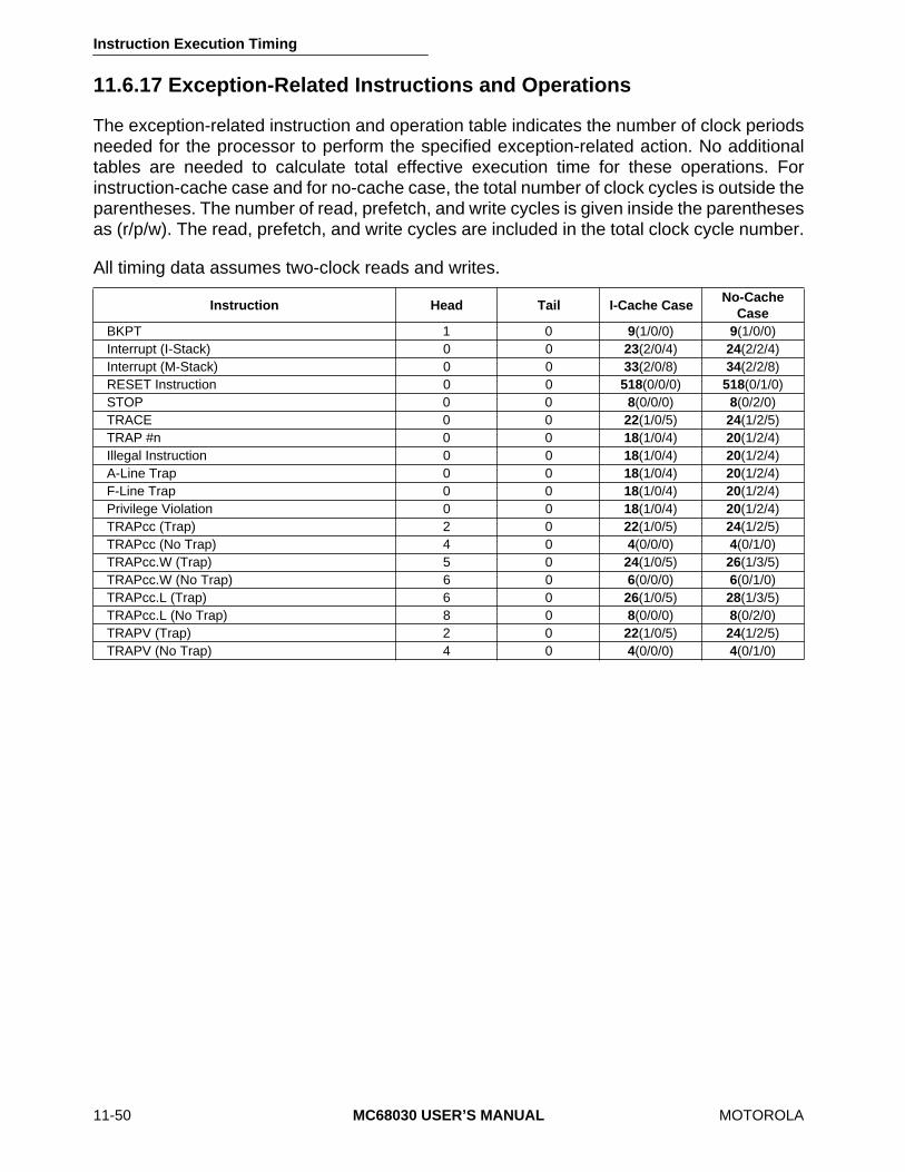
Instruction Execution Timing
11-50 MC68030 USER’S MANUAL MOTOROLA
11.6.17 Exception-Related Instructions and Operations
The exception-related instruction and operation table indicates the number of clock periodsneeded for the processor to perform the specified exception-related action. No additionaltables are needed to calculate total effective execution time for these operations. Forinstruction-cache case and for no-cache case, the total number of clock cycles is outside theparentheses. The number of read, prefetch, and write cycles is given inside the parenthesesas (r/p/w). The read, prefetch, and write cycles are included in the total clock cycle number.
All timing data assumes two-clock reads and writes.
Instruction Head Tail I-Cache CaseNo-Cache
CaseBKPT 1 0 9(1/0/0) 9(1/0/0)Interrupt (I-Stack) 0 0 23(2/0/4) 24(2/2/4)Interrupt (M-Stack) 0 0 33(2/0/8) 34(2/2/8)RESET Instruction 0 0 518(0/0/0) 518(0/1/0)STOP 0 0 8(0/0/0) 8(0/2/0)TRACE 0 0 22(1/0/5) 24(1/2/5)TRAP #n 0 0 18(1/0/4) 20(1/2/4)Illegal Instruction 0 0 18(1/0/4) 20(1/2/4)A-Line Trap 0 0 18(1/0/4) 20(1/2/4)F-Line Trap 0 0 18(1/0/4) 20(1/2/4)Privilege Violation 0 0 18(1/0/4) 20(1/2/4)TRAPcc (Trap) 2 0 22(1/0/5) 24(1/2/5)TRAPcc (No Trap) 4 0 4(0/0/0) 4(0/1/0)TRAPcc.W (Trap) 5 0 24(1/0/5) 26(1/3/5)TRAPcc.W (No Trap) 6 0 6(0/0/0) 6(0/1/0)TRAPcc.L (Trap) 6 0 26(1/0/5) 28(1/3/5)TRAPcc.L (No Trap) 8 0 8(0/0/0) 8(0/2/0)TRAPV (Trap) 2 0 22(1/0/5) 24(1/2/5)TRAPV (No Trap) 4 0 4(0/0/0) 4(0/1/0)
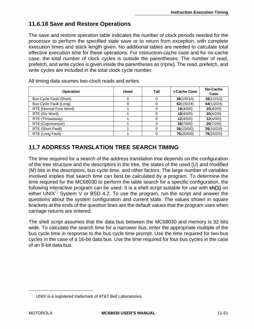
Instruction Execution Timing
MOTOROLA MC68030 USER’S MANUAL 11-51
11.6.18 Save and Restore Operations
The save and restore operation table indicates the number of clock periods needed for theprocessor to perform the specified state save or to return from exception, with completeexecution times and stack length given. No additional tables are needed to calculate totaleffective execution time for these operations. For instruction-cache case and for no-cachecase, the total number of clock cycles is outside the parentheses. The number of read,prefetch, and write cycles is given inside the parentheses as (r/p/w). The read, prefetch, andwrite cycles are included in the total clock cycle number.
All timing data ssumes two-clock reads and writes.
11.7 ADDRESS TRANSLATION TREE SEARCH TIMING
The time required for a search of the address translation tree depends on the configurationof the tree structure and the descriptors in the tree, the states of the used (U) and modified(M) bits in the descriptors, bus cycle time, and other factors. The large number of variablesinvolved implies that search time can best be calculated by a program. To determine thetime required for the MC68030 to perform the table search for a specific configuration, thefollowing interactive program can be used. It is a shell script suitable for use with sh(1) oneither UNIX System V or BSD 4.2. To use the program, run the script and answer thequestions about the system configuration and current state. The values shown in squarebrackets at the ends of the question lines are the default values that the program uses whencarriage returns are entered.
The shell script assumes that the data bus between the MC68030 and memory is 32 bitswide. To calculate the search time for a narrower bus, enter the appropriate multiple of thebus cycle time in response to the bus cycle time prompt. Use the time required for two buscycles in the case of a 16-bit data bus. Use the time required for four bus cycles in the caseof an 8-bit data bus.
UNIX is a registered trademark of AT&T Bell Laboratories.
Operation Head Tail I-Cache CaseNo-Cache
CaseBus Cycle Fault (Short) 0 0 36(1/0/10) 38(1/2/10)Bus Cycle Fault (Long) 0 0 62(1/0/24) 64(1/2/24)RTE (Normal Four Word) 1 0 18(4/0/0) 20(4/2/0) RTE (Six Word) 1 0 18(4/0/0) 20(4/2/0) RTE (Throwaway) 1 0 12(4/0/0) 12(4/0/0)RTE (Coprocessor) 1 0 26(7/0/0) 26(7/2/0) RTE (Short Fault) 1 0 36(10/0/0) 26(10/2/0)RTE (Long Fault) 1 0 76(25/0/0) 76(25/2/0)

Instruction Execution Timing
11-52 MC68030 USER’S MANUAL MOTOROLA
The times provided by this program include all phases of the translation tree search. Withvarious mask versions of the MC68030, times may differ slightly from those calculated bythe program.
(UNABLE TO LOCATE ART)

Instruction Execution Timing
MOTOROLA MC68030 USER’S MANUAL 11-53
(UNABLE TO LOCATE ART)
Instruction Execution Timing
11-54 MC68030 USER’S MANUAL MOTOROLA
(UNABLE TO LOCATE ART)

Instruction Execution Timing
MOTOROLA MC68030 USER’S MANUAL 11-55
(UNABLE TO LOCATE ART)
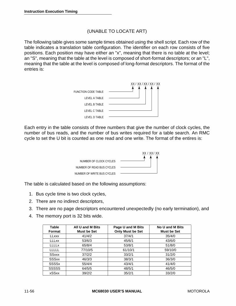
Instruction Execution Timing
11-56 MC68030 USER’S MANUAL MOTOROLA
The following table gives some sample times obtained using the shell script. Each row of thetable indicates a translation table configuration. The identifier on each row consists of fivepositions. Each position may have either an "x", meaning that there is no table at the level;an "S", meaning that the table at the level is composed of short-format descriptors; or an "L",meaning that the table at the level is composed of long-format descriptors. The format of theentries is:
Each entry in the table consists of three numbers that give the number of clock cycles, thenumber of bus reads, and the number of bus writes required for a table search. An RMCcycle to set the U bit is counted as one read and one write. The format of the entires is:
The table is calculated based on the following assumptions:
1. Bus cycle time is two clock cycles,
2. There are no indirect descriptors,
3. There are no page descriptors encountered unexpectedly (no early termination), and
4. The memory port is 32 bits wide.
(UNABLE TO LOCATE ART)
Table Format
All U and M Bits Must be Set
Page U and M BitsOnly Must be Set
No U and M BitsMust be Set
LLxxx 41/4/2 37/4/1 35/4/0LLLxx 53/6/3 45/6/1 43/6/0LLLLx 65/8/4 53/8/1 51/8/0LLLLL 77/10/5 61/10/1 59/10/0SSxxx 37/2/2 33/2/1 31/2/0SSSxx 46/3/3 38/3/1 36/3/0SSSSx 55/4/4 43/4/1 41/4/0SSSSS 64/5/5 48/5/1 46/5/0xSSxx 39/2/2 35/2/1 33/2/0
XX XX/ /XX
FUNCTION CODE TABLE
XX/XX/
LEVEL A TABLE
LEVEL B TABLE
LEVEL C TABLE
LEVEL D TABLE
XX XX XX/ /
NUMBER OF CLOCK CYCLES
NUMBER OF READ BUS CYCLES
NUMBER OF WRITE BUS CYCLES
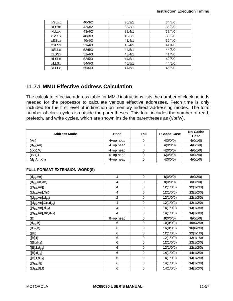
Instruction Execution Timing
MOTOROLA MC68030 USER’S MANUAL 11-57
11.7.1 MMU Effective Address Calculation
The calculate effective address table for MMU instructions lists the number of clock periodsneeded for the processor to calculate various effective addresses. Fetch time is onlyincluded for the first level of indirection on memory indirect addressing modes. The totalnumber of clock cycles is outside the parentheses. This total includes the number of read,prefetch, and write cycles, which are shown inside the parentheses as (r/pr/w).
xSLxx 40/3/2 36/3/1 34/3/0xLSxx 42/3/2 38/3/1 36/3/0xLLxx 43/4/2 39/4/1 37/4/0xSSSx 48/3/3 40/3/1 38/3/0xSSLx 49/4/3 41/4/1 39/4/0xSLSx 51/4/3 43/4/1 41/4/0xSLLx 52/5/3 44/5/1 44/5/0xLSSx 51/4/3 43/4/1 41/4/0xLSLx 52/5/3 44/5/1 42/5/0xLLSx 54/5/3 46/5/1 44/5/0xLLLx 55/6/3 47/6/1 45/6/0
Address Mode Head Tail I-Cache CaseNo-Cache
Case(An) 4+op head 0 4(0/0/0) 4(0/1/0)(d16,An) 4+op head 0 4(0/0/0) 4(0/1/0)
(xxx).W 4+op head 0 4(0/0/0) 4(0/1/0)(xxx).L 6+op head 0 6(0/0/0) 6(0/2/0)(d8,An,Xn) 4+op head 0 4(0/0/0) 4(0/1/0)
FULL FORMAT EXTENSION WORD(S)
(d16,An) 4 0 8(0/0/0) 8(0/2/0)
(d16,An,Xn) 4 0 8(0/0/0) 8(0/2/0)
([d16,An]) 4 0 12(1/0/0) 12(1/2/0)
([d16,An],Xn) 4 0 12(1/0/0) 12(1/2/0)
([d16,An],d16) 2 0 12(1/0/0) 12(1/2/0)
([d16,An],Xn,d16) 4 0 12(1/0/0) 12(1/2/0)
([d16,An],d32) 4 0 14(1/0/0) 14(1/3/0)
([d16,An],Xn,d32) 4 0 14(1/0/0) 14(1/3/0)
(B) 8+op head 0 8(0/0/0) 8(0/1/0)(d16,B) 6 0 10(0/0/0) 10(0/2/0)
(d32,B) 6 0 16(0/0/0) 16(0/2/0)
([B]) 6 0 12(1/0/0) 12(1/1/0)([B],I) 6 0 12(1/0/0) 12(1/1/0)([B],d16) 6 0 12(1/0/0) 12(1/2/0)
([B],I,d16) 6 0 12(1/0/0) 12(1/2/0)
([B],d32) 6 0 14(1/0/0) 14(1/2/0)
([B],I,d32) 6 0 14(1/0/0) 14(1/2/0)
([d16,B]) 6 0 14(1/0/0) 14(1/2/0)
([d16,B],I) 6 0 14(1/0/0) 14(1/2/0)

Instruction Execution Timing
11-58 MC68030 USER’S MANUAL MOTOROLA
([d16,B],d16) 6 0 14(1/0/0) 14(1/2/0)
([d16,B],I,d16) 6 0 14(1/0/0) 14(1/2/0)
([d16,B],I,d32) 6 0 16(1/0/0) 16(1/3/0)
FULL FORMAT EXTENSION WORD(S)

Instruction Execution Timing
MOTOROLA MC68030 USER’S MANUAL 11-59
11.7.1 MMU Effective Address Calculation (Continued)
B = Base address; O, An, Xn, An+Xn. Form does not affect timing.I = Index; O, Xn*No separation on effective address and operation in timing. Head and tail are the operation's.NOTE: Xn cannot be in B and I at the same time. Scaling and size of Xn do not affect timing.
Address Mode Head Tail I-Cache Case No-Cache Case
FULL FORMAT EXTENSION WORD(S)
([d32,B]) 6 0 20(1/0/0) 20(1/2/0)
([d32,B],I) 6 0 20(1/0/0) 20(1/2/0)
([d32,B],d16) 6 0 20(1/0/0) 20(1/3/0)
([d32,B],I,d16) 6 0 20(1/0/0) 20(1/3/0)
([d32,B],d32) 6 0 22(1/0/0) 22(1/3/0)
([d32,B],I,d32) 6 0 22(1/0/0) 22(1/3/0)
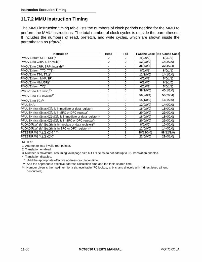
Instruction Execution Timing
11-60 MC68030 USER’S MANUAL MOTOROLA
11.7.2 MMU Instruction Timing
The MMU instruction timing table lists the numbers of clock periods needed for the MMU toperform the MMU instructions. The total number of clock cycles is outside the parentheses.It includes the numbers of read, prefetch, and write cycles, which are shown inside theparentheses as (r/pr/w).
NOTES:1. Attempt to load invalid root pointer.2. Translation enabled.3. Number is maximum, assuming valid page size but TIx fields do not add up to 32. Translation enabled.4. Translation disabled. * Add the appropriate effective address calculation time. ** Add the appropriate effective address calculation time and the table search time.*** Number given is the maximum for a six-level table (FC lookup, a, b, c, and d levels with indirect level, all long
descriptors).
Instruction Head Tail I-Cache Case No-Cache CasePMOVE (from CRP, SRP)* 0 0 4(0/0/2) 5(0/1/2)PMOVE (to CRP, SRP, valid)* 0 0 12(2/0/0) 14(2/2/0)
PMOVE (to CRP, SRP, invalid)1* 0 0 28(3/0/4) 30(3/2/4)
PMOVE (from TT0, TT1)* 0 0 8(0/0/1) 8(0/1/1)PMOVE (to TT0, TT1)* 0 0 12(1/0/0) 14(1/2/0)PMOVE (from MMUSR)* 2 0 4(0/0/1) 5(0/1/1)PMOVE (to MMUSR)* 0 0 6(1/0/0) 6(1/1/0)PMOVE (from TC)* 2 0 4(0/0/1) 5(0/1/1)
PMOVE (to TC, valid)2* 0 0 38(1/0/0) 40(1/2/0)
PMOVE (to TC, invalid)3* 0 0 56(2/0/4) 58(2/2/4)
PMOVE (to TC)4* 0 0 14(1/0/0) 16(1/2/0)
PFLUSHA 0 0 12(0/0/0) 14(0/2/0)PFLUSH (fc),#⟨mask⟩ (fc is immediate or data register) 0 0 16(0/0/0) 18(0/2/0)PFLUSH (fc),#⟨mask⟩ (fc is in SFC or DFC register) 0 0 20(0/0/0) 22(0/2/0)PFLUSH (fc),#⟨mask⟩,⟨ea⟩ (fc is immediate or data register)* 0 0 16(0/0/0) 18(0/2/0)PFLUSH (fc),#⟨mask⟩,⟨ea⟩ (fc is in SFC or DFC register)* 0 0 20(0/0/0) 22(0/2/0)PLOAD[R:W] (fc),⟨ea⟩ (fc is immediate or data register)** 0 0 8(0/0/0) 10(0/2/0)PLOAD[R:W] (fc),⟨ea⟩ (fc is in SFC or DFC register)** 0 0 12(0/0/0) 14(0/2/0)PTEST[R:W] (fc),⟨ea⟩,#6 * *** 0 1 88(12/0/0) 88(12/1/0)PTEST[R:W] (fc),⟨ea⟩,#0* 0 0 22(0/0/0) 22(0/1/0)
Instruction Execution Timing
MOTOROLA MC68030 USER’S MANUAL 11-61
11.8 INTERRUPT LATENCY
In real-time systems, the response time required for a processor to service an interrupt is avery important factor pertaining to overall system performance. Processors in the M68000Family support asynchronous assertion of interrupts and begin processing them onsubsequent instruction boundaries. The average interrupt latency is quite short, but themaximum latency is often critical because real-time interrupts cannot require servicing inless than the maximum interrupt latency. The maximum interrupt latency for the MC68030alone is approximately 200 clock cycles (for the MOVEM.L ([d32,An],Xn,d32), D0-D7/A0-A7instruction where the last data fetch is aborted with a bus error), but when the MMU isenabled, some operations can take several times longer to execute.
Interrupt latency in systems using the MMU is affected by the length of the main processorinstructions, the address translation tree configuration, the number of translation treesearches required by the instructions, the access time of main memory, and the width of thedata bus connecting the MC68030 to main memory. It is important to note that the addresstranslation tree configuration is under software control and can strongly affect the systeminterrupt latency. The maximum interrupt latency for a given system configuration can becomputed by adding the length of the longest main processor instruction to the time requiredfor the maximum number of translation tree searches that the instruction could require. Forthe MC68030 microprocessor, one instruction of particular interest is a memory-to-memorymove with memory indirect addressing for both the source and destination, with all of thecode and data items crossing page boundaries. The assembler syntax for this instruction is:
MOVE.L (od,[bd,An,Rm]),(od,[bd,An,Rm])
This instruction can cause ten address translation tree searches: two for the instructionstream, two for the source indirect address, two for the destination indirect address, two forthe operand fetch, and two for the destination write. System software can reduce themaximum number of translation searches by placing additional restrictions on generatedcode. For example, if the language translators in the system only generate long wordsaligned on long-word boundaries, the indirect address and operands can cause only onetranslation search each. This reduces the number of searches for the instruction to amaximum of six.
Instruction Execution Timing
11-62 MC68030 USER’S MANUAL MOTOROLA
11.9 BUS ARBITRATION LATENCY
In a system that uses the MMU, the bus arbitration latency is affected by several factors.The MC68030 does not relinquish the physical bus while it is performing a read-modify-writeoperation. Since the address translation search is an extended read-modify-write operation,the no-cache-case latency is incurred by the longest address translation search required bythe system.
Another bus arbitration delay occurs when a coprocessor or other device delays or fails toassert DSACKx or STERM signals to terminate a bus cycle. The maximum delay in this caseis undefined; it depends on the length of the delay in asserting the signals.

MOTOROLA
MC68030 USER’S MANUAL
12-1
SECTION 12APPLICATIONS INFORMATION
This section provides guidelines for using the MC68030. First, it discusses the requirementsfor adapting the MC68030 to MC68020 designs. Then, it describes the use of the MC68881and MC68882 coprocessors with the MC68030. The byte select logic is described next,followed by memory interface information. A description of external caches, the use of theSTATUS and REFILL signals, and power and ground considerations complete the section.
12.1 ADAPTING THE MC68030 TO MC68020 DESIGNS
Perhaps the easiest way to first utilize the MC68030 is in a system designed for theMC68020. This is possible due to the complete compatibility of the asynchronous buses ofthe MC68020 and MC68030. This section describes how to configure an adapter for theMC68030 to allow insertion into an existing MC68020-based system. Software andarchitectural differences between the two processors are also discussed. The need for anadapter is absolute because the MC68020 and MC68030 are NOT pin compatible. Use ofthe adapter board provides the immediate capability for evaluating the programmer's modeland instruction set of the MC68030 and for developing software to utilize the MC68030'sadditional enhanced features. This adapter board also provides a relatively simple methodfor increasing the performance of an existing MC68020 or MC68020/MC68851 system byinsertion of a more advanced 32-bit MPU with an on-chip data cache and an on-chip MMU.Since the adapter board does not support of the synchronous bus interface of the MC68030,performance measurements for the MC68030 used in this manner may be misleading whencompared to a system designed specifically for the MC68030.
The adapter board plugs into the CPU socket of an MC68020 target system, drawing power,ground, and clock signals through the socket and running bus cycles in a fashion compatiblewith the MC68030. The only support hardware necessary is a single 1K-ohm pullup resistorand two capacitors for decoupling power and ground on the adapter board.
Applications Information
12-2
MC68030 USER’S MANUAL
MOTOROLA
12.1.1 Signal Routing
Figure 12-1 shows the complete schematic for routing the signals of the MC68030 to theMC68020 header. All signals common to both processors are directly routed to thecorresponding signal of the other processor. The signals on the MC68030 that do not havea compatible signal on the MC68020 are either pulled up or left unconnected:
Pulled Up No Connect
TERM STATUS
CBACK REFILL
CIIN CBREQ
MMUDIS CIOUT
12.1.2 Hardware Differences
Before enabling the on-chip caches of the MC68030, an important system feature must bechecked. Because of the MC68030 cache organization and implementation, cachable readbus cycles are expected to transfer the entire port width of data (as indicated by the DSACKxencoding), regardless of how many bytes are actually requested by the SIZx pins. TheMC68020 did not have this requirement, and system memory banks or peripherals may ormay not supply the amount of data required by the MC68030. If the target system does notsupply the full port width with valid data for any cachable instruction or data access the usershould either designate that area of memory as noncachable (with the MMU) or not enablethe corresponding on-chip cache(s). In some systems, modifying the target systemhardware may also be an option; frequently, the byte select logic is generated by a singlePAL, which might easily be replaced or reprogrammed to select all bytes during read cyclesfrom multibyte ports.
The HALT input-only signal of the MC68030 is slightly different than the bidirectional HALTsignal of the MC68020. However, this should not cause any problems beyond eliminatingan indication to the external system (e.g., lighting an LED) that the processor has halted dueto a double bus fault.
When used in a system originally designed for both an MC68020 and an MC68851, theMC68851 may be left in the system or removed (and replaced with a jumpered header).However, if left in the system, the MC68851 is not accessible to the programmer with theM68000 coprocessor interface. All MMU instructions access the MC68030's on-chip MMU.This is true even if the MC68030's MMUDIS signal is asserted. The benefit in removing theMC68851 is that the minimum asynchronous bus cycle time to the physical bus is reducedfrom four clock cycles to three.

Applications Information
MOTOROLA
MC68030 USER’S MANUAL
12-3
Figure 12-1. Signal Routing for Adapting the MC68030 to MC68020 Designs
STATUSREFILL
IPL2IPL1IPL0IPENDAVEC
CLK
RESET
ECSOCS
CDISCIOUTCBREQCBACKCIIN
STERM
BRBGBGACK
HALTBERR
DSACK1DSACK0
SIZ0SIZ1
RMCDBENR/WDSAS
D31–D0
FC2–FC0
A31–A0
IPL2IPL1IPL0
IPENDAVEC
CLK
RESET
ECSOCS
CDIS
BRBG
BGACK
HALTBERR
DSACK1DSACK0
SIZ0SIZ1
RMCDBEN
R/WDSAS
D31–D0
FC2–FC0
A31–A0
MC68EC030 MC68020 HEADER
1k
Applications Information
12-4
MC68030 USER’S MANUAL
MOTOROLA
If the MC68851 is removed and replaced with a jumpered header, the following MC68851signals may need special system-specific consideration: CLI, RMC, LBRO, LBG, LBGACK,and LBGI. During translation table searches, the MC68851 asserts the cache load inhibit(CLI) signal but not RMC; whereas, the MC68030 asserts RMC but not CIOUT. In simpleMC68020/MC68851 systems without logical bus arbitration or logical caches, theMC68851's jumper can have the following signals connected together:
LAS
↔
PAS
LBRO
↔
PBR
LBGI
↔
PBG
LBGACK
↔
PBGACK
LA(8-31)
↔
PA(8-31)
CLI
↔
no connect or LAS
CLI has two connection options because some systems may use CLI to qualify theoccurrence of CPU space cycles since the MC68851's PAS does not assert.
12.1.3 Software Differences
The instruction cache control bits in the cache control register (CACR) of the MC68030 arein the identical bit positions as the corresponding bits as the MC68020's CACR. However,the MC68030 has additional control bits for burst enable and data cache control. Becausethis adapter board does not support synchronous bus cycles (and thus burst mode),enabling burst mode through the CACR does not affect system operation in any way. Referto
Section 6 On-Chip Cache Memories
for more information on the bit positions andfunctions of the CACR bits.
When used in a system originally designed for an MC68020, a difference a programmermust be aware of is that the MC68030 does not support the CALLM and RTM instructionsof the MC68020. If code is executed on the MC68030 using either the CALLM or RTMinstructions, an unimplemented instruction exception is taken. If no MMU softwaredevelopment capability is desired and the cache behavior described under hardwaredifferences is understood, the user may ignore the MC68030 MMU.
When the adapter is used in a system originally designed for the MC68020/MC68851 pair,the software differences described below also apply. The MC68030's MMU offers a subsetof the MC68851 features. The features not supported by the MC68030 MMU are listed be-low:
• On-chip breakpoint registers
• Task aliasing
• Instructions: PBcc, PDBcc, PRESTORE, PSAVE, PScc, PTRAPcc, PVALID
Applications Information
MOTOROLA
MC68030 USER’S MANUAL
12-5
Only control-alterable addressing modes are allowed for MMU instructions on the MC68030.
A feature new to the MC68030 MMU (and not on the MC68851) is the transparenttranslation of two logical address blocks with the transparent translation registers. See
Section 9 Memory Management Unit
.
12.2 FLOATING-POINT UNITS
Floating-point support for the MC68030 is provided by the MC68881 floating-pointcoprocessor and the MC68882 enhanced floating-point coprocessor. Both devices offer afull implementation of the
IEEE Standard for Binary Floating-Point Arithmetic
(754). TheMC68882 is a pin and software-compatible upgrade of the MC68881, with an optimizedMPU interface that provides over 1.5 times the performance of the MC68881 at the sameclock frequency.
Both coprocessors provide a logical extension to the integer data processing capabilities ofthe main processor. They contain a very high performance floating-point arithmetic unit anda set of floating-point data registers that are utilized in a manner that is analagous to the useof the integer data registers of the processor. The MC68881/MC68882 instruction set is anatural extension of all earlier members of the M68000 Family and supports all of theaddressing modes and data types of the host MC68030. The programmer perceives theMC68030/coprocessor execution model as if both devices are implemented on one chip. Inaddition to supporting the full IEEE standard, the MC68881 and MC68882 provide a full setof trigonometric and transcendental functions, on-chip constants, and a full 80-bit extended-precision-real data format.
The interface of the MC68030 to the MC68881 or the MC68882 is easily tailored to systemcost/performance needs. The MC68030 and the MC68881/MC68882 communicate viastandard asynchronous M68000 bus cycles. All data transfers are performed by the mainprocessor at the request of the MC68881/MC68882; thus memory management, bus errors,address errors, and bus arbitration function as if the MC68881/MC68882 instructions areexecuted by the main processor. The floating-point unit and the processor may operate atdifferent clock speeds, and up to seven floating-point coprocessors may reside in anMC68030 system simultaneously.
Figure 12-2 illustrates the coprocessor interface connection of an MC68881/MC68882 to anMC68030 (uses entire 32-bit data bus). The MC68881/MC68882 is configured to operatewith a 32-bit data bus when both the A0 SIZE and pins are connected to V
CC
. Refer to theMC68881UM/AD
MC68881/MC68882 Floating-Point Coprocessor User's Manual
forconfiguring the MC68881/MC68882 for smaller data bus widths. Note that the MC68030cache inhibit input (CIIN) signal is not used for the coprocessor interface because theMC68030 does not cache data obtained during CPU space accesses.
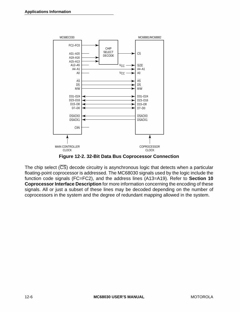
Applications Information
12-6
MC68030 USER’S MANUAL
MOTOROLA
The chip select (CS) decode circuitry is asynchronous logic that detects when a particularfloating-point coprocessor is addressed. The MC68030 signals used by the logic include thefunction code signals (FC=FC2), and the address lines (A13=A19). Refer to
Section 10Coprocessor Interface Description
for more information concerning the encoding of thesesignals. All or just a subset of these lines may be decoded depending on the number ofcoprocessors in the system and the degree of redundant mapping allowed in the system.
Figure 12-2. 32-Bit Data Bus Coprocessor Connection
MC68EC030 MC68881/MC68882
CHIPSELECTDECODE
FC2–FC0
A31–A20A19–A16A15–A13
A12–A5A4–A1
A0
ASDS
R/W
D31–D24D23–D16D15–D8
D7–D0
DSACK0DSACK1
CIIN
MAIN CONTROLLERCLOCK
CS
SIZEA4–A1A0
ASDSR/W
D31–D24D23–D16D15–D8D7–D0
DSACK0DSACK1
COPROCESSORCLOCK
VCC
VCC

Applications Information
MOTOROLA
MC68030 USER’S MANUAL
12-7
The major concern of a system designer is to design a CS interface that meets the ACelectrical specifications for both the MC68030 (MPU) and the MC68881/MC68882 (FPCP)without adding unnecessary wait states to FPCP accesses. The following maximumspecifications (relative to CLK low) meet these objectives:
t
CLK
low to AS low
≤
(MPU Spec 1–MPU Spec 47A–FPCP Spec 19) (1)
t
CLK
low to CS low
≤
(MPU Spec 1–MPU Spec 47A–FPCP Spec 19) (2)
Even though requirement (1) is not met under worst case conditions, if the MPU AS isloaded within specifications and the AS input to the FPCP is unbuffered, the requirement ismet under typical conditions. Designing the CS generation circuit to meet requirement (2)provides the highest probability that accesses to the FPCP occur without unnecessary waitstates. A PAL 16L8 (see Figure 12-3) with a maximum propagation delay of 10 ns,programmed according to the equations in Figure 12-4, can be used to generate CS. For a25-MHz system,
t
CLK low to CS low is less than or equal to 10 ns when this design is used.Should worst case conditions cause t
CLK
low to AS low to exceed requirement (1), one waitstate is inserted in the access to the FPCP; no other adverse effect occurs. Figure 12-5shows the bus cycle timing for this interface. Refer to MC68881UM/AD,
MC68881/MC68882Floating-Point Coprocessor User's Manual
, for FPCP specifications.
The circuit that generates CS must meet another requirement. When a nonfloating-pointaccess immediately follows a floating-point access, CS (for the floating-point access) mustbe negated before AS and DS (for the subsequent access) are asserted. The PAL circuitpreviously described also meets this requirement.
For example, if a system has only one coprocessor, the full decoding of the ten signals(FC0–FC2 and A13–A19) provided by the PAL equations in Figure 12-4 is not absolutelynecessary. It may be sufficient to use only FC0–FC1 and A16–A17. FC0–FC1 indicate whena bus cycle is operating in either CPU space ($7) or user-defined space ($3), and A16–A17encode CPU space type as coprocessor space ($2). A13–A15 can be ignored in this casebecause they encode the coprocessor identification code (CpID) used to differentiatebetween multiple coprocessors in a system. Motorola assemblers always default to a CpIDof $1 for floating-point instructions; this can be controlled with assembler directives if adifferent CpID is desired or if multiple coprocessors exist in the system.
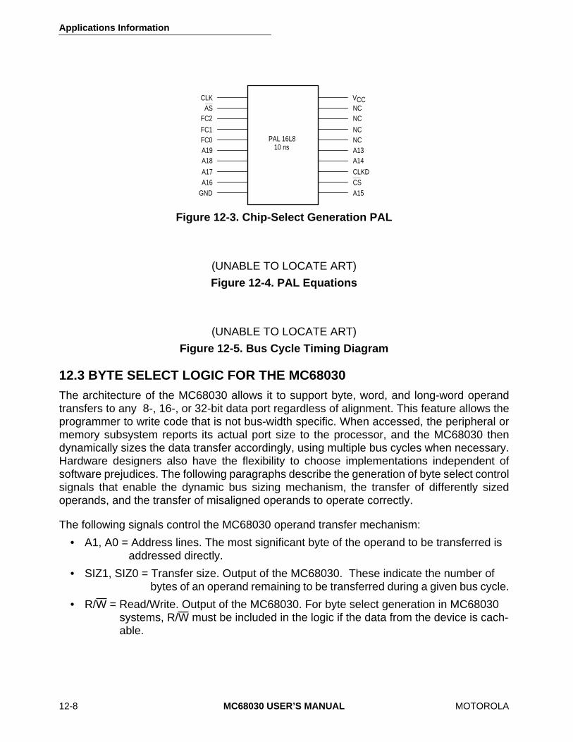
Applications Information
12-8
MC68030 USER’S MANUAL
MOTOROLA
12.3 BYTE SELECT LOGIC FOR THE MC68030
The architecture of the MC68030 allows it to support byte, word, and long-word operandtransfers to any 8-, 16-, or 32-bit data port regardless of alignment. This feature allows theprogrammer to write code that is not bus-width specific. When accessed, the peripheral ormemory subsystem reports its actual port size to the processor, and the MC68030 thendynamically sizes the data transfer accordingly, using multiple bus cycles when necessary.Hardware designers also have the flexibility to choose implementations independent ofsoftware prejudices. The following paragraphs describe the generation of byte select controlsignals that enable the dynamic bus sizing mechanism, the transfer of differently sizedoperands, and the transfer of misaligned operands to operate correctly.
The following signals control the MC68030 operand transfer mechanism:
• A1, A0 = Address lines. The most significant byte of the operand to be transferred is addressed directly.
• SIZ1, SIZ0 = Transfer size. Output of the MC68030. These indicate the number of bytes of an operand remaining to be transferred during a given bus cycle.
• R/W = Read/Write. Output of the MC68030. For byte select generation in MC68030 systems, R/W must be included in the logic if the data from the device is cach-able.
Figure 12-3. Chip-Select Generation PAL
(UNABLE TO LOCATE ART)
Figure 12-4. PAL Equations
(UNABLE TO LOCATE ART)
Figure 12-5. Bus Cycle Timing Diagram
CLKAS
FC2
FC1FC0A19A18
A17A16
GND
VNCNC
NCNCA13A14
CLKDCSA15
CC
PAL 16L810 ns

Applications Information
MOTOROLA
MC68030 USER’S MANUAL
12-9
• DSACK1, DSACK0 = Data transfer and size acknowledge. Driven by an asynchronous port to indicate the actual bus width of the port.
• STERM = Synchronous termination. Driven by a 32-bit synchronous port only.
The MC68030 assumes that 16-bit ports are situated on data lines D16–D31, and that 8-bitports are situated on data lines D24–D31. This ensures that the following logic workscorrectly with the MC68030's on-chip internal-to-external data bus multiplexer. Refer to
Section 7 Bus Operation
for more details on the dynamic bus sizing mechanism.
The need for byte select signals is best illustrated by an example. Consider a long-wordwrite cycle to an odd address in word-organized memory. The transfer requires three buscycles to complete. The first bus cycle transfers the most significant byte of the long wordon D16–D23. The second bus cycle transfers a word on D16–D31, and the last bus cycletransfers the least significant byte of the original long word on D24–D31. In order not tooverwrite those bytes which are not used these transfers, a unique byte data strobe must begenerated for each byte when using devices with 16- and 32-bit port widths.
For noncachable read cycles and all write cycles, the required active bytes of the data busfor any given bus transfer are a function of the size (SIZ0/SIZ1) and lower address (A0/A1)outputs and are shown in Table 12-1. Individual strobes or select signals can be generatedby decoding these four signals for every bus cycle. Devices residing on 8-bit ports can utilizedata strobe (DS) alone since there is only one valid byte for any transfer.
During cachable read cycles, the addressed device must provide valid data over its full buswidth (as indicated by DSACKx or STERM). While instructions are always prefetched aslong-word-aligned accesses, data fetches can occur with any alignment and size. Becausethe MC68030 assumes that the entire data bus port size contains valid data, cachable dataread bus cycles must provide as much data as signaled by the port size during a bus cycle.To satisfy this requirement, the R/W signal must be included in the byte select logic for theMC68030.
Figure 12-6 shows a block diagram of an MC68030 system with two memory banks. ThePAL provides memory-mapped byte select signals for an asynchronous 32-bit port andunmapped byte select signals for other memory banks or ports. Figure 12-7 provides sampleequations for the PAL.
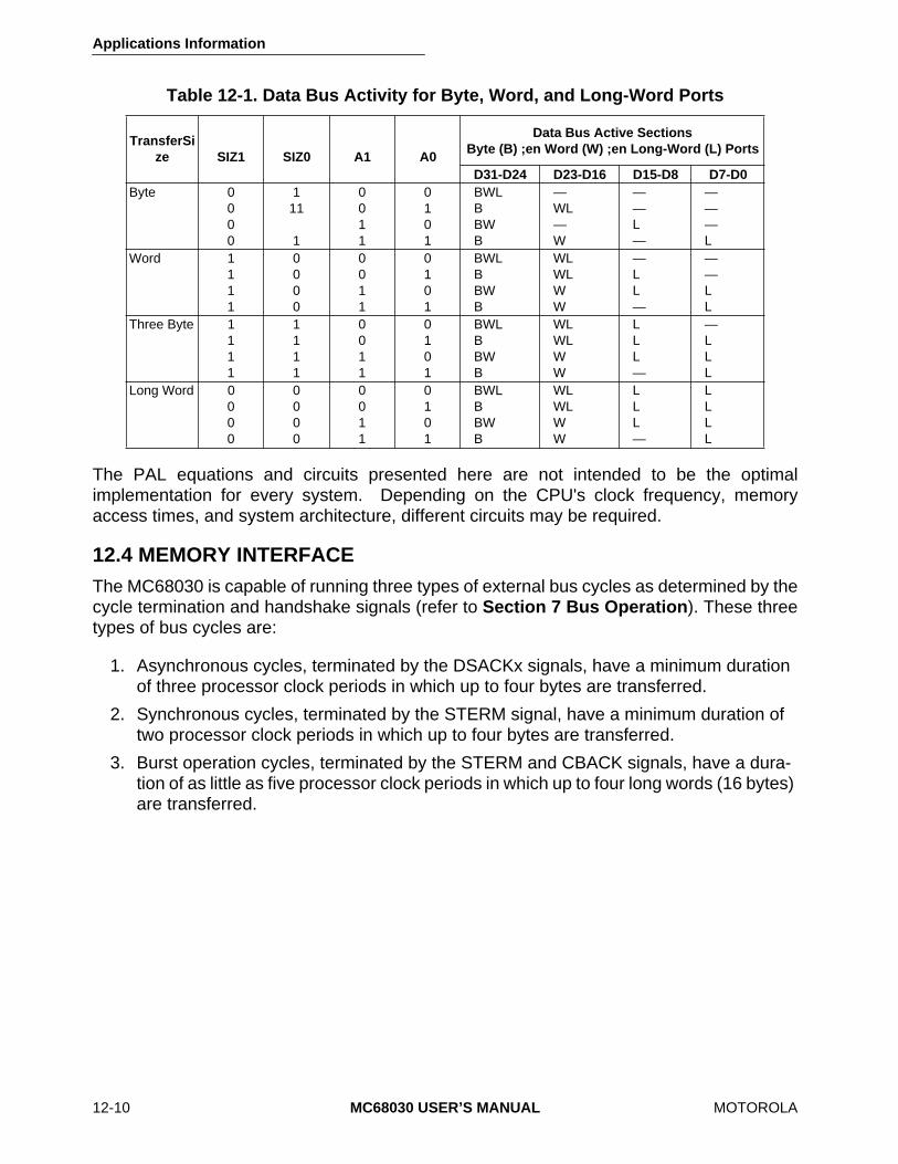
Applications Information
12-10
MC68030 USER’S MANUAL
MOTOROLA
The PAL equations and circuits presented here are not intended to be the optimalimplementation for every system. Depending on the CPU's clock frequency, memoryaccess times, and system architecture, different circuits may be required.
12.4 MEMORY INTERFACE
The MC68030 is capable of running three types of external bus cycles as determined by thecycle termination and handshake signals (refer to
Section 7 Bus Operation
). These threetypes of bus cycles are:
1. Asynchronous cycles, terminated by the DSACKx signals, have a minimum duration of three processor clock periods in which up to four bytes are transferred.
2. Synchronous cycles, terminated by the STERM signal, have a minimum duration of two processor clock periods in which up to four bytes are transferred.
3. Burst operation cycles, terminated by the STERM and CBACK signals, have a dura-tion of as little as five processor clock periods in which up to four long words (16 bytes) are transferred.
Table 12-1. Data Bus Activity for Byte, Word, and Long-Word Ports
TransferSize SIZ1 SIZ0 A1 A0
Data Bus Active SectionsByte (B) ;en Word (W) ;en Long-Word (L) Ports
D31-D24 D23-D16 D15-D8 D7-D0
Byte 0000
111
1
0011
0101
BWLBBWB
—WL—W
——L—
———L
Word 1111
0000
0011
0101
BWLBBWB
WLWLWW
—LL—
——LL
Three Byte 1111
1111
0011
0101
BWLBBWB
WLWLWW
LLL—
—LLL
Long Word 0000
0000
0011
0101
BWLBBWB
WLWLWW
LLL—
LLLL
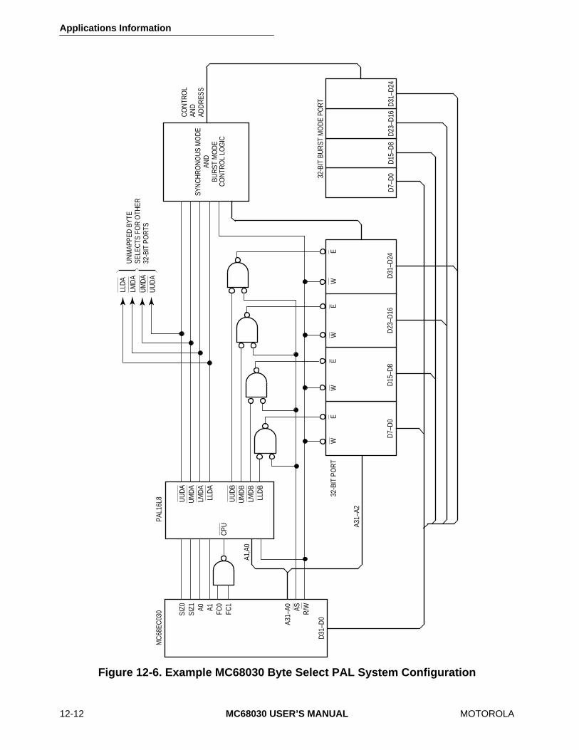
Applications Information
12-12
MC68030 USER’S MANUAL
MOTOROLA
Figure 12-6. Example MC68030 Byte Select PAL System Configuration
SYN
CH
RO
NO
US
MO
DE
AND
BUR
ST M
OD
EC
ON
TRO
L LO
GIC
UU
DA
UM
DA
LMD
ALL
DA
UU
DB
UM
DB
LMD
BLL
DB
MC
68EC
030
PAL1
6L8
D7–
D0
D15
–D8
D23
–D16
D31
–D24
WE
WE
WE
WE
A31–
A2
32-B
IT P
OR
T
32-B
IT B
UR
ST M
OD
E PO
RT
D7–
D0
D15
–D8
D23
–D16
D31
–D24
CO
NTR
OL
AND
ADD
RES
S
LLD
ALM
DA
UM
DA
UU
DA
UN
MAP
PED
BYT
ESE
LEC
TS F
OR
OTH
ER32
-BIT
PO
RTS
CPU
A1,A
0
SIZ0
SIZ1 A0 A1 FC0
FC1
A31–
A0 AS R/W
D31
–D0
Applications Information
MOTOROLA
MC68030 USER’S MANUAL
12-13
During read operations, M68000 processors latch data on the last falling clock edge of thebus cycle, one-half clock before the bus cycle ends (burst mode is a special case). Latchingdata here, instead of the next rising clock edge, helps to avoid data bus contention with thenext bus cycle and allows the MC68030 to receive the data into its execution unit sooner fora net performance increase.
Write operations also use this data bus timing to allow data hold times from the negatingstrobes and to avoid any bus contention with the following bus cycle. This usually allows thesystem to be designed with a minimum of bus buffers and latches.
One of the benefits of the MC68030's on-chip caches is that the effect of external wait stateson performance is lessened because the caches are always accessed in fewer than “no waitstates” regardless of the external memory configuration. This feature makes the MC68030(and MC68020) unique among other general-purpose microprocessors.
12.4.1 Access Time Calculations
The timing paths that are typically critical in any memory interface are illustrated and definedin Figure 12-8. For burst transfers, the first long word transferred also uses theseparameters, but the subsequent transfers are different and are discussed in
12.4.2 BurstMode Cycles
.
The type of device that is interfaced to the MC68030 determines exactly which of the pathsis most critical. The address-to-data paths are typically the critical paths for static devicessince there is no penalty for initiating a cycle to these devices and later validating that accesswith the appropriate bus control signal. Conversely, the address-strobe-to-data-valid path isoften most critical for dynamic devices since the cycle must be validated before an accesscan be initiated. For devices that signal termination of a bus cycle before data is validated(e.g., error detection and correction hardware and some external caches) to improveperformance, the critical path may be from the address or strobes to the assertion of BERR(or BERR and HALT). Finally, the address-valid-to-DSACKx-or-STERM-asserted path ismost critical for very fast devices and external caches, since the time available betweenwhen the address is valid and when DSACKx or STERM must be asserted to terminate thebus cycle is minimal. Table 12-2 provides the equations required to calculate the variousmemory access times assuming a 50-percent duty cycle clock.
(UNABLE TO LOCATE ART)
Figure 12-7. MC68030 Byte Select PAL Equations
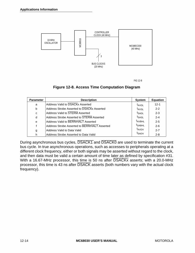
Applications Information
12-14
MC68030 USER’S MANUAL
MOTOROLA
During asynchronous bus cycles, DSACK1 and DSACK0 are used to terminate the currentbus cycle. In true asynchronous operations, such as accesses to peripherals operating at adifferent clock frequency, either or both signals may be asserted without regard to the clock,and then data must be valid a certain amount of time later as defined by specification #31.With a 16.67-MHz processor, this time is 50 ns after DSACKx asserts; with a 20.0-MHzprocessor, this time is 43 ns after DSACK asserts (both numbers vary with the actual clockfrequency).
Figure 12-8. Access Time Computation Diagram
Parameter Description System Equation
a
b
c
d
e
f
g
h
Address Valid to DSACKx Asserted
Address Strobe Asserted to DSACKx Asserted
Address Valid to STERM Asserted
Address Strobe Asserted to STERM Asserted
Address Valid to BERR/HALT Asserted
Address Strobe Asserted to BERR/HALT Asserted
Address Valid to Data Valid
Address Strobe Asserted to Data Valid
t
AVDL
t
AVSL
t
SADL
t
SASL
t
AVBHL
t
SABHL
t
AVDV
t
SADV
12-1
2-2
2-3
2-4
2-5
2-6
2-7
2-8
MC68EC030(40 MHz)
10-MHzOSCILLATOR
CONTROLLERCLOCK (40 MHz)
BUS CLOCKS(20 MHz)
3
FIG 12-8M
C88
916
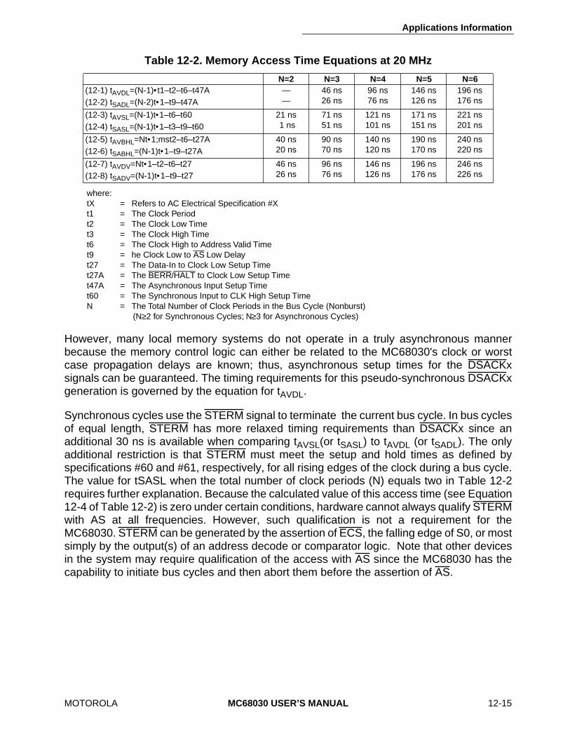
Applications Information
MOTOROLA
MC68030 USER’S MANUAL
12-15
where:tX = Refers to AC Electrical Specification #Xt1 = The Clock Periodt2 = The Clock Low Timet3 = The Clock High Timet6 = The Clock High to Address Valid Timet9 = he Clock Low to AS Low Delayt27 = The Data-In to Clock Low Setup Timet27A = The BERR/HALT to Clock Low Setup Timet47A = The Asynchronous Input Setup Timet60 = The Synchronous Input to CLK High Setup TimeN = The Total Number of Clock Periods in the Bus Cycle (Nonburst)
(N
≥
2 for Synchronous Cycles; N
≥
3 for Asynchronous Cycles)
However, many local memory systems do not operate in a truly asynchronous mannerbecause the memory control logic can either be related to the MC68030's clock or worstcase propagation delays are known; thus, asynchronous setup times for the DSACKxsignals can be guaranteed. The timing requirements for this pseudo-synchronous DSACKxgeneration is governed by the equation for t
AVDL
.
Synchronous cycles use the STERM signal to terminate the current bus cycle. In bus cyclesof equal length, STERM has more relaxed timing requirements than DSACKx since anadditional 30 ns is available when comparing t
AVSL
(or t
SASL
) to t
AVDL
(or t
SADL
). The onlyadditional restriction is that STERM must meet the setup and hold times as defined byspecifications #60 and #61, respectively, for all rising edges of the clock during a bus cycle.The value for tSASL when the total number of clock periods (N) equals two in Table 12-2requires further explanation. Because the calculated value of this access time (see Equation12-4 of Table 12-2) is zero under certain conditions, hardware cannot always qualify STERMwith AS at all frequencies. However, such qualification is not a requirement for theMC68030. STERM can be generated by the assertion of ECS, the falling edge of S0, or mostsimply by the output(s) of an address decode or comparator logic. Note that other devicesin the system may require qualification of the access with AS since the MC68030 has thecapability to initiate bus cycles and then abort them before the assertion of AS.
Table 12-2. Memory Access Time Equations at 20 MHz
N=2 N=3 N=4 N=5 N=6
(12-1) t
AVDL
=(N-1)
•
t1–t2–t6–t47A(12-2) t
SADL
=(N-2)t
•
1–t9–t47A——
46 ns26 ns
96 ns76 ns
146 ns126 ns
196 ns176 ns
(12-3) t
AVSL
=(N-1)t
•
1–t6–t60(12-4) t
SASL=(N-1)t•1–t3–t9–t6021 ns 1 ns
71 ns51 ns
121 ns101 ns
171 ns151 ns
221 ns201 ns
(12-5) tAVBHL=Nt•1;mst2–t6–t27A(12-6) tSABHL=(N-1)t•1–t9–t27A
40 ns20 ns
90 ns70 ns
140 ns120 ns
190 ns170 ns
240 ns220 ns
(12-7) tAVDV=Nt•1–t2–t6–t27(12-8) tSADV=(N-1)t•1–t9–t27
46 ns26 ns
96 ns76 ns
146 ns126 ns
196 ns176 ns
246 ns226 ns
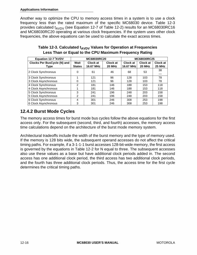
Applications Information
12-16 MC68030 USER’S MANUAL MOTOROLA
Another way to optimize the CPU to memory access times in a system is to use a clockfrequency less than the rated maximum of the specific MC68030 device. Table 12-3provides calculated tAVDV (see Equation 12-7 of Table 12-2) results for an MC68030RC16and MC68030RC20 operating at various clock frequencies. If the system uses other clockfrequencies, the above equations can be used to calculate the exact access times.
12.4.2 Burst Mode CyclesThe memory access times for burst mode bus cycles follow the above equations for the firstaccess only. For the subsequent (second, third, and fourth) accesses, the memory accesstime calculations depend on the architecture of the burst mode memory system.
Architectural tradeoffs include the width of the burst memory and the type of memory used.If the memory is 128 bits wide, the subsequent operand accesses do not affect the criticaltiming paths. For example, if a 3-1-1-1 burst accesses 128-bit-wide memory, the first accessis governed by the equations in Table 12-2 for N equal to three. The subsequent accessesalso use these values as a base but have additional clock periods added in. The secondaccess has one additional clock period, the third access has two additional clock periods,and the fourth has three additional clock periods. Thus, the access time for the first cycledetermines the critical timing paths.
Table 12-3. Calculated tAVDV Values for Operation at FrequenciesLess Than or Equal to the CPU Maximum Frequency Rating
Equation 12-7 tAVDV MC68030RC20 MC68030RC25Clocks Per BusCycle (N) and
TypeWait
StatesClock at
16.67 MHzClock at 20 MHz
Clock at 16.67 MHz
Clock at 20 MHz
Clock at 25 MHz
2 Clock Synchronous 0 61 46 68 5338—
3 Clock Synchronous3 Clock Asynchronous
10
121121
9696
128128
103103
7878
4 Clock Synchronous4 Clock Asynchronous
21
181181
146146
188188
153153
118118
5 Clock Synchronous5 Clock Asynchronous
32
241241
196196
248248
203203
158158
6 Clock Synchronous6 Clock Asynchronous
43
301301
246246
308308
253253
198198

Applications Information
MOTOROLA MC68030 USER’S MANUAL 12-17
Memory that is 64 bits wide presents a compromise between the two configurations listedabove.
12.5 STATIC RAM MEMORY BANKSWhen the MC68030 is operating at a high clock frequency, a no-wait-state external memorysystem will most likely be composed of static RAMs. The following paragraphs discuss threestatic memory banks, which may be used as shown or as a starting point for an externalcache design. The designs offer different levels of performance, bus utilization, and cost.
12.5.1 A Two-Clock Synchronous Memory Bank Using SRAMSThe MC68030 normally attains its highest performance when the external memory systemcan support a two-clock synchronous bus protocol. This section describes a completememory bank containing 64K bytes that can operate with a 20-MHz MC68030 using two-clock accesses. Also discussed are several options and minor alterations to reduce cost orpower consumption.
Figure 12-9 shows the complete memory bank and its connection to the MC68030. Asdrawn, the required parts include:
(8) 16K•4 SRAMs, 35-ns access time with separate I/O pins
(4) 74F244 buffers
(2) 74F32 OR gates
(1) PAL16L8D (or equivalent)
The system must also provide any STERM consolidation circuitry as required (e.g., by thepresence of multiple synchronous memory banks or ports). In Figure 12-9, this consolidationcircuitry is shown as an AND gate.
The memory bank can be divided into three sections:
1. The byte select and address decode section (provided by the PAL),
2. The actual memory section (SRAMs), and
3. The buffer section.
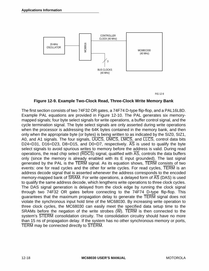
Applications Information
12-18 MC68030 USER’S MANUAL MOTOROLA
The first section consists of two 74F32 OR gates, a 74F74 D-type flip-flop, and a PAL16L8D.Example PAL equations are provided in Figure 12-10. The PAL generates six memory-mapped signals; four byte select signals for write operations, a buffer control signal, and thecycle termination signal. The byte select signals are only asserted during write operationswhen the processor is addressing the 64K bytes contained in the memory bank, and thenonly when the appropriate byte (or bytes) is being written to as indicated by the SIZ0, SIZ1,A0, and A1 signals. The four signals, UUCS, UMCS, LMCS, and LLCS, control data bitsD24=D31, D16=D23, D8=D15, and D0=D7, respectively. AS is used to qualify the byteselect signals to avoid spurious writes to memory before the address is valid. During readoperations, the read chip select (RDCS) signal, qualified with AS, controls the data buffersonly (since the memory is already enabled with its E input grounded). The last signalgenerated by the PAL is the TERM signal. As its equation shows, TERM consists of twoevents: one for read cycles and the other for write cycles. For read cycles, TERM is anaddress decode signal that is asserted whenever the address corresponds to the encodedmemory-mapped bank of SRAM. For write operations, a delayed form of AS (DAS) is usedto qualify the same address decode, which lengthens write operations to three clock cycles.The DAS signal generation is delayed from the clock edge by running the clock signalthrough two 74F32 OR gates before connecting to the 74F74 D-type flip-flop. Thisguarantees that the maximum propagation delay to generate the TERM signal does notviolate the synchronous input hold time of the MC68030. By increasing write operation tothree clock cycles, the MC68030 can easily meet the specified data setup time to theSRAMs before the negation of the write strobes (W). TERM is then connected to thesystem's STERM consolidation circuity. The consolidation circuitry should have no morethan 15 ns of propagation delay. If the system has no other synchronous memory or ports,TERM may be connected directly to STERM.
Figure 12-9. Example Two-Clock Read, Three-Clock Write Memory Bank
MC68EC030(40 MHz)
20-MHzOSCILLATOR
CONTROLLERCLOCK (40 MHz)
BUS CLOCKS(40 MHz)
3
MC
8891
6
FIG 12-9
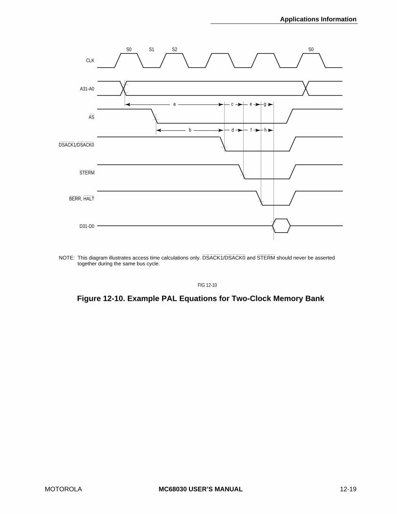
Applications Information
MOTOROLA MC68030 USER’S MANUAL 12-19
Figure 12-10. Example PAL Equations for Two-Clock Memory Bank
CLK
A31-A0
FIG 12-10
S0 S1 S2 S0
AS
DSACK1/DSACK0
STERM
a c e g
b d f h
BERR, HALT
D31-D0
NOTE: This diagram illustrates access time calculations only. DSACK1/DSACK0 and STERM should never be asserted together during the same bus cycle.
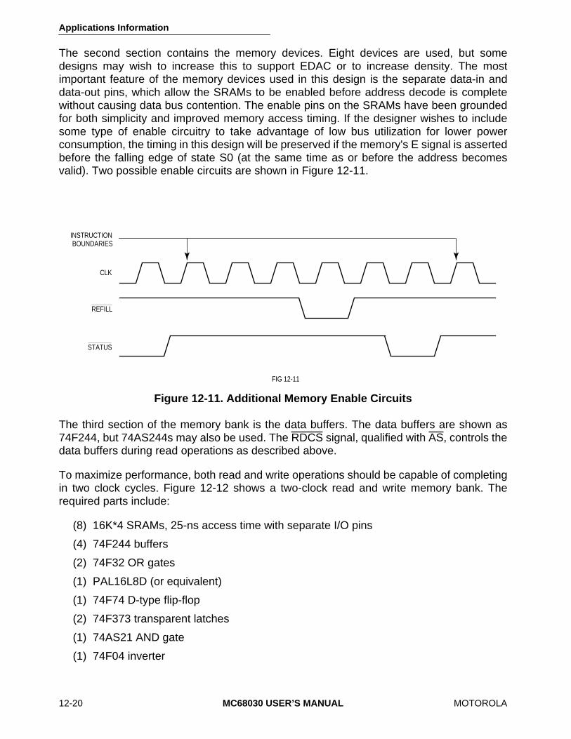
Applications Information
12-20 MC68030 USER’S MANUAL MOTOROLA
The second section contains the memory devices. Eight devices are used, but somedesigns may wish to increase this to support EDAC or to increase density. The mostimportant feature of the memory devices used in this design is the separate data-in anddata-out pins, which allow the SRAMs to be enabled before address decode is completewithout causing data bus contention. The enable pins on the SRAMs have been groundedfor both simplicity and improved memory access timing. If the designer wishes to includesome type of enable circuitry to take advantage of low bus utilization for lower powerconsumption, the timing in this design will be preserved if the memory's E signal is assertedbefore the falling edge of state S0 (at the same time as or before the address becomesvalid). Two possible enable circuits are shown in Figure 12-11.
The third section of the memory bank is the data buffers. The data buffers are shown as74F244, but 74AS244s may also be used. The RDCS signal, qualified with AS, controls thedata buffers during read operations as described above.
To maximize performance, both read and write operations should be capable of completingin two clock cycles. Figure 12-12 shows a two-clock read and write memory bank. Therequired parts include:
(8) 16K*4 SRAMs, 25-ns access time with separate I/O pins
(4) 74F244 buffers
(2) 74F32 OR gates
(1) PAL16L8D (or equivalent)
(1) 74F74 D-type flip-flop
(2) 74F373 transparent latches
(1) 74AS21 AND gate
(1) 74F04 inverter
Figure 12-11. Additional Memory Enable Circuits
CLK
REFILL
STATUS
INSTRUCTIONBOUNDARIES
FIG 12-11

Applications Information
MOTOROLA MC68030 USER’S MANUAL 12-21
The structure of this design is very similiar to the previous design and can similarly bedivided into three main sections:
1. The byte select and address decode section (provided by the PAL).
2. The actual memory section (SRAMs).
3. The buffer/latch section (address and data).
The same PAL equations listed in Figure 12-10 are used with the exception of the TERMsignal. Figure 12-13 shows the equation for TERM, which is used by the two clock read andwrite design.
TERM = /A16 * /A17 * /A16 * A30 ;immediate STERM for both reads and writes
Figure 12-13. Example PAL Equation for Two-Clock Read and WriteMemory Bank
TERM is simply an address decode signal in this design because both read and writeoperations complete in two clock periods. The other signals generated by the PAL havealready been discussed in the previous design and are not repeated here. A latched versionof AS is generated by a 74F74 D-type flip-flop and used to qualify the individual byte selectsignals from the PAL. The required SRAM data setup time on write cycles is ensured bykeeping the write strobes (W) active to the SRAMs until the rising edge of the clock thatcompletes the MC68030 write operation.
The memory section in this design uses 25-ns SRAMs rather than the 35-ns SRAMs usedin the previous design. The faster SRAMs compensate for the 74F373 transparent latchesused on the address lines. Since the memory write operations complete after the MC68030write bus cycle, both address and data are latched and held valid to the SRAMs until thewrite strobes (W) negate. During read operations, the transparent latches on the addresslines remain in the transparent mode, allowing the SRAMs to provide data through the74F244 buffers in time to meet the specified data setup time to the MC68030.
Figure 12-12. Example Two-Clock Read and Write Memory Bank
CLK
REFILL
STATUS
INSTRUCTIONBOUNDARIES
FIG 12-12
PENDING TRACE ORINTERRUPT EXCEPTIONPROCESSING
Applications Information
12-22 MC68030 USER’S MANUAL MOTOROLA
Not all systems require the performance of 20-MHz two-clock bus cycles, nor will all systemsbe able to afford the fast devices. Fortunately, several small changes to this design couldassist designers with different cost/performance ratios. The simplest and most directmethod is to reduce the clock frequency of the MC68030. For instance, if the clockfrequency is below approximately 18.1 MHz, the same control logic supports two-clock buscycles with 45-ns memory (55 ns if < 15.8 MHz). If 20 MHz is still the frequency of choice,the designer may choose to run three-clock bus cycles. This can be accomplished with theaddition of a flip-flop to delay the TERM signal by one clock. The resulting memory accesstime is over 85 ns with a 20-MHz processor running with three-clock bus cycles.
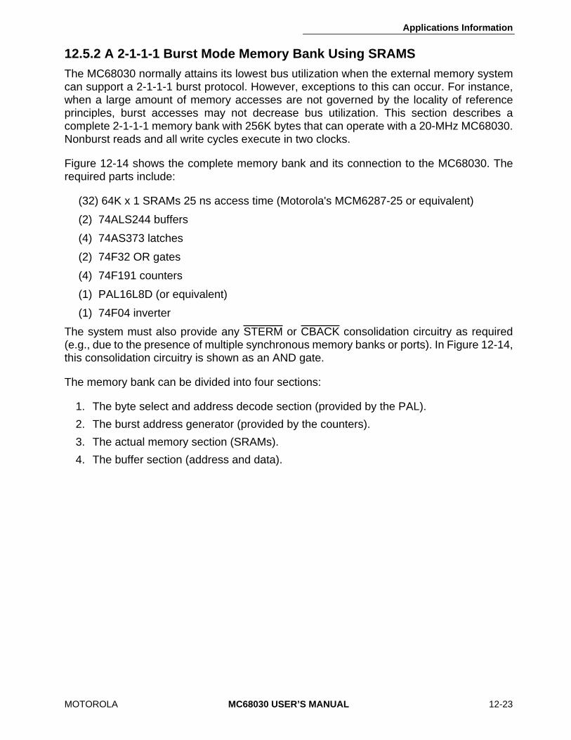
Applications Information
MOTOROLA MC68030 USER’S MANUAL 12-23
12.5.2 A 2-1-1-1 Burst Mode Memory Bank Using SRAMSThe MC68030 normally attains its lowest bus utilization when the external memory systemcan support a 2-1-1-1 burst protocol. However, exceptions to this can occur. For instance,when a large amount of memory accesses are not governed by the locality of referenceprinciples, burst accesses may not decrease bus utilization. This section describes acomplete 2-1-1-1 memory bank with 256K bytes that can operate with a 20-MHz MC68030.Nonburst reads and all write cycles execute in two clocks.
Figure 12-14 shows the complete memory bank and its connection to the MC68030. Therequired parts include:
(32) 64K x 1 SRAMs 25 ns access time (Motorola's MCM6287-25 or equivalent)
(2) 74ALS244 buffers
(4) 74AS373 latches
(2) 74F32 OR gates
(4) 74F191 counters
(1) PAL16L8D (or equivalent)
(1) 74F04 inverter
The system must also provide any STERM or CBACK consolidation circuitry as required(e.g., due to the presence of multiple synchronous memory banks or ports). In Figure 12-14,this consolidation circuitry is shown as an AND gate.
The memory bank can be divided into four sections:
1. The byte select and address decode section (provided by the PAL).
2. The burst address generator (provided by the counters).
3. The actual memory section (SRAMs).
4. The buffer section (address and data).
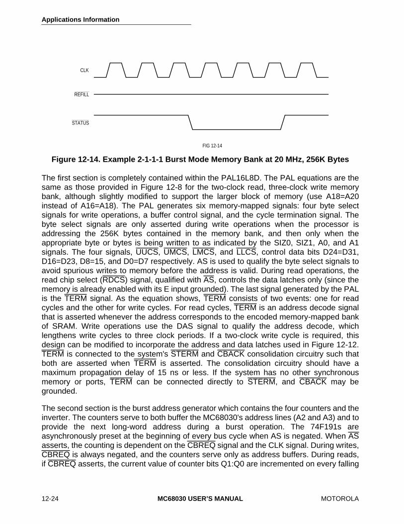
Applications Information
12-24 MC68030 USER’S MANUAL MOTOROLA
The first section is completely contained within the PAL16L8D. The PAL equations are thesame as those provided in Figure 12-8 for the two-clock read, three-clock write memorybank, although slightly modified to support the larger block of memory (use A18=A20instead of A16=A18). The PAL generates six memory-mapped signals: four byte selectsignals for write operations, a buffer control signal, and the cycle termination signal. Thebyte select signals are only asserted during write operations when the processor isaddressing the 256K bytes contained in the memory bank, and then only when theappropriate byte or bytes is being written to as indicated by the SIZ0, SIZ1, A0, and A1signals. The four signals, UUCS, UMCS, LMCS, and LLCS, control data bits D24=D31,D16=D23, D8=15, and D0=D7 respectively. AS is used to qualify the byte select signals toavoid spurious writes to memory before the address is valid. During read operations, theread chip select (RDCS) signal, qualified with AS, controls the data latches only (since thememory is already enabled with its E input grounded). The last signal generated by the PALis the TERM signal. As the equation shows, TERM consists of two events: one for readcycles and the other for write cycles. For read cycles, TERM is an address decode signalthat is asserted whenever the address corresponds to the encoded memory-mapped bankof SRAM. Write operations use the DAS signal to qualify the address decode, whichlengthens write cycles to three clock periods. If a two-clock write cycle is required, thisdesign can be modified to incorporate the address and data latches used in Figure 12-12.TERM is connected to the system's STERM and CBACK consolidation circuitry such thatboth are asserted when TERM is asserted. The consolidation circuitry should have amaximum propagation delay of 15 ns or less. If the system has no other synchronousmemory or ports, TERM can be connected directly to STERM, and CBACK may begrounded.
The second section is the burst address generator which contains the four counters and theinverter. The counters serve to both buffer the MC68030's address lines (A2 and A3) and toprovide the next long-word address during a burst operation. The 74F191s areasynchronously preset at the beginning of every bus cycle when AS is negated. When ASasserts, the counting is dependent on the CBREQ signal and the CLK signal. During writes,CBREQ is always negated, and the counters serve only as address buffers. During reads,if CBREQ asserts, the current value of counter bits Q1:Q0 are incremented on every falling
Figure 12-14. Example 2-1-1-1 Burst Mode Memory Bank at 20 MHz, 256K Bytes
CLK
REFILL
STATUS
FIG 12-14

Applications Information
MOTOROLA MC68030 USER’S MANUAL 12-25
clock edge of the MC68030's clock after AS asserts. Four counters are used to provideenough drive capability to avoid an additional buffer propagation delay. Each counter driveseight memory devices.
The third section contains the memory devices. The most important feature of the memorydevices used in this design is the separate data-in and data-out pins, which allow theSRAMs to be constantly enabled before address decode is complete without causing databus contention. If the designer wishes to include some type of enable circuitry to takeadvantage of low bus utilization, the timing in this design will be preserved if the memory'sE signal is asserted within 13 ns after the falling edge of state S0.
Applications Information
12-26 MC68030 USER’S MANUAL MOTOROLA
The fourth and last section of the memory bank is the address and data buffers. The addressbuffers are shown as 74ALS244s, but 74AS244s and 74F244s are also acceptable. Twoinputs to the address buffers remain unused allowing the possibility for expansion up to 1Mbyte without any additional devices when SRAMs of suitable density become available.The RDCS signal, qualified with AS, controls the data buffers during read operations. Theaddress buffers are always enabled.
Some modifications to this design can improve performance. Specifically, circuitry to controlCBACK and thus prevent or discontinue a burst cycle is a simple addition. The circuitryshould have two functions: to prevent wraparound and to prevent bursting when a dataoperand crosses a long-word boundary.
Not all systems require the performance of 20-MHz 2-1-1-1 burst cycles, nor will all systemsbe able to afford the fast devices of this design. If the clock frequency is below approximately17.5 MHz, the same support logic supports 2-1-1-1 burst cycles with 35-ns memory. If 20MHz is still the frequency of choice, the designer may choose to run 3-1-1-1 burst cycles.
12.5.3 A 3-1-1-1 Burst Mode Memory Bank Using SRAMSFigure 12-15 shows the complete 3-1-1-1 memory bank with 256K bytes that can operatewith a 20-MHz MC68030. The required parts include:
(32) 64K x 1 SRAMs 35-ns access time (Motorola's MCM6287-35 or equivalent)
(4) 74ALS244 buffers
(4) 74F374 latches
(2) 74F32 OR gates
(4) 74F191 counters
(1) PAL16L8D (or equivalent)
(2) inverters
(1) flip-flop
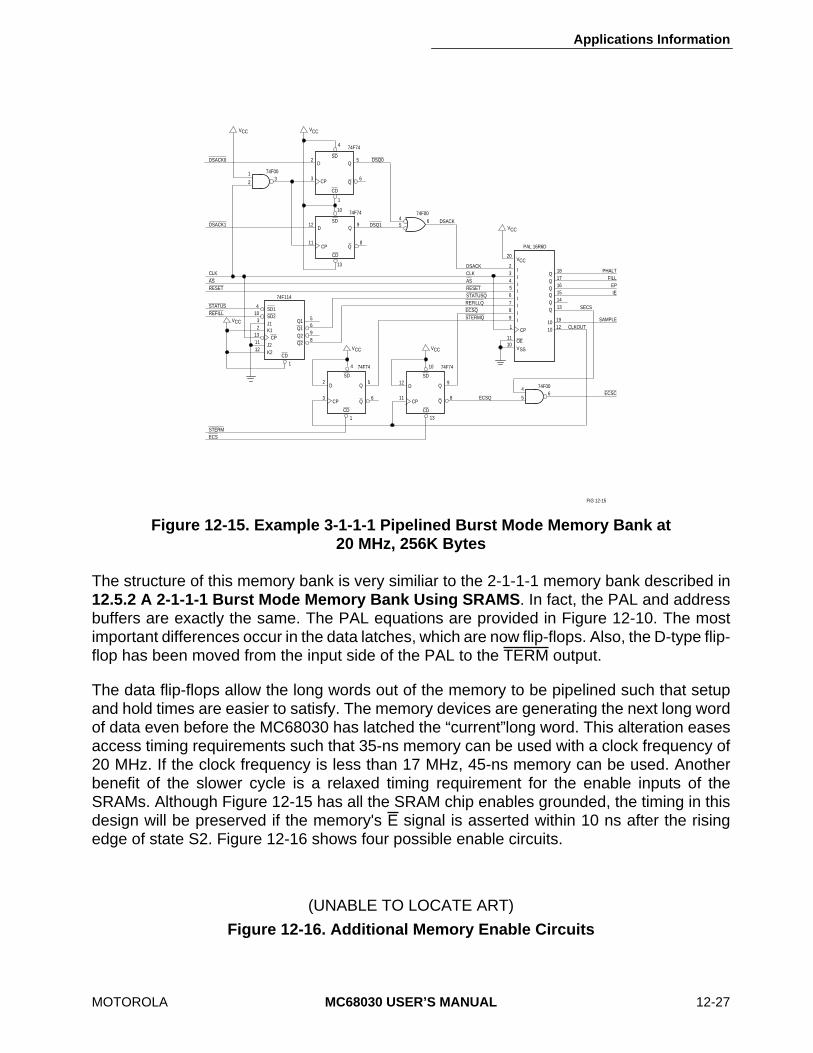
Applications Information
MOTOROLA MC68030 USER’S MANUAL 12-27
The structure of this memory bank is very similiar to the 2-1-1-1 memory bank described in12.5.2 A 2-1-1-1 Burst Mode Memory Bank Using SRAMS. In fact, the PAL and addressbuffers are exactly the same. The PAL equations are provided in Figure 12-10. The mostimportant differences occur in the data latches, which are now flip-flops. Also, the D-type flip-flop has been moved from the input side of the PAL to the TERM output.
The data flip-flops allow the long words out of the memory to be pipelined such that setupand hold times are easier to satisfy. The memory devices are generating the next long wordof data even before the MC68030 has latched the “current”long word. This alteration easesaccess timing requirements such that 35-ns memory can be used with a clock frequency of20 MHz. If the clock frequency is less than 17 MHz, 45-ns memory can be used. Anotherbenefit of the slower cycle is a relaxed timing requirement for the enable inputs of theSRAMs. Although Figure 12-15 has all the SRAM chip enables grounded, the timing in thisdesign will be preserved if the memory's E signal is asserted within 10 ns after the risingedge of state S2. Figure 12-16 shows four possible enable circuits.
Figure 12-15. Example 3-1-1-1 Pipelined Burst Mode Memory Bank at20 MHz, 256K Bytes
(UNABLE TO LOCATE ART)
Figure 12-16. Additional Memory Enable Circuits
STATUSQ
VCC
IIIIIIII SAMPLE
CLKOUT
20
QQQQQQ
23456
789
181716151413
1912
SECS
PHALTFILL
EPIE
PAL 16R6D
VCC
1
1110
VSS
OE
CP
1010
6
2
33
DSQ0
SDQ
Q
CD
CP
D9
SDQ
Q
CD
CP
D5
DSACK
13
VCC
DSACK0
1
2
74F00
DSACK1 12
11 8
DSQ1
74F004 65
VCC
CLK
ASRESET
REFILLQ
STERMQ
ECSC
SD
Q
Q
CD
CP
D9
VCC
10 74F74
8
13
12
11
SD
Q
Q
CD
CP
D5
VCC
4 74F74
6
1
2
3
74F004
56
ECSQ
STERMECS
SD1SD2J1K1 CPJ2K2
Q1Q1Q2Q2
410
32
131112
98
56
CD
VCC
STATUSREFILL
74F114
1
10 74F74
74F744
DSACKCLKASRESET
ECSQ
1
FIG 12-15
Applications Information
12-28 MC68030 USER’S MANUAL MOTOROLA
The flip-flop connected to the TERM signal serves two purposes: first, the TERM signal isdelayed at the beginning of the cycle to insert the wait state for the first long word, andsecond, the burst address generator is also prevented from incrementing the long word baseaddress until the first long-word has been latched by the 74F374s.
The performance enhancing modifications described for the 2-1-1-1 design also apply to thisdesign. Specifically, circuitry can be added to control CBACK and thus prevent ordiscontinue a burst cycle. The circuitry should have two functions: first, to preventwraparound and second, to prevent bursting when a data operand crosses a long-wordboundary. Another enhancement might be to alter the TERM control circuitry with theaddition of a write latch mechanism to run two-clock writes.
The critical path for the 3-1-1-1 memory bank is not the first long-word access as in the 2-1-1-1 memory bank, but rather the subsequent long words during burst cycles. No alternativearchitecture can correct the critical path for the 2-1-1-1 burst cycle. However, for 3-1-1-1burst cycles, the designer might consider memory banks which are 64 or 128 bits wide. Inthis manner, the access time for the subsequent long words can be hidden underneath theaccess of the previous long word(s).
12.6 EXTERNAL CACHESTo provide lower average access times to memory, some systems implement caches localto the main processor that store recently used instructions and/or data. For the MC68030,several architectural options are available to the cache designer. The primary decisions arewhether to configure the cache as an asynchronous or synchronous device and whether thecache accesses are terminated early (before the cache lookup is complete) or only aftervalidation.
The MC68030 late BERR/HALT facility allows an external device to signal completion of abus cycle by asserting DSACKx or STERM and later (approximately one clock period orone-half clock, respectively) aborting or retrying that cycle if an error condition is detected.Since one critical access path in many memory structures is the assertion of DSACKx/STERM to avoid additional wait states, the late abort capability allows the memory controllerto terminate a bus cycle before data is valid on the processor data bus. If the data validationfails, the memory controller can then abort (BERR) or retry (BERR/HALT) the cycle. Thistechnique is useful in memory error detection schemes where the cycle can be terminatedas soon as data becomes available and the error checking can occur during the periodbetween the signaling of termination of the cycle and the latching of data by the processorwith a late retry or abort signaled upon error indication. Likewise, this technique can be usedin cache implementations in which the cache tag validation cannot be completed beforetermination of the cycle must be signaled but the validation is completed before late abort orretry must be indicated.
The major consideration in choosing whether or not to utilize late retry for an external cachemiss is the overhead involved in retrying a bus cycle after a miss in the cache. The minimumpenalty is the four clock periods required to retry the cycle (two clocks during which the missis detected and two clocks idle bus time), assuming that the bus control strobes (BERR andHALT) are negated soon enough after the completion of the aborted cycle that the next cyclecan begin immediately. In evaluating this overhead, the projected cache miss rate

Applications Information
MOTOROLA MC68030 USER’S MANUAL 12-29
determines the percentage of cycles that must be retried. Additionally, the degree ofparallelism in the system should be considered. If, after a cache miss, it is possible tocontinue the bus cycle to main memory while the processor is retrying the cycle, it is possibleto avoid some, or all, of the performance penalty associated with late retry (although thecontrol circuitry required may be more complex).
Applications Information
12-30 MC68030 USER’S MANUAL MOTOROLA
For a two-clock bus or burst capability, use of the synchronous bus is mandated, but for athree or more clock, nonburst cache, the choice of synchronous versus asynchronousoperation must be made. If the bus cycle is terminated only after validation, use of thesynchronous bus is recommended since the address-valid-to-STERM-asserted timingrequirement is longer than the address-valid-to-DSACK-asserted timing for bus cycles of thesame length. If the cache implements late retry, the choice of which bus control mode to useis less important and depends on system-specific features and control structures. Someexternal caches might use both synchronous and asynchronous transfers: synchronous forhits and asynchronous for misses or vice versa. The following discussion assumes that theexternal cache uses the synchronous two-clock protocol, but most statements also apply tothe asynchronous protocol.
If the MC68030 MMU is disabled, all bus cycles use logical addresses. If the MMU isenabled, the external address bus uses physical addresses (including directly mappedlogical-to-physical addresses from the transparent translation (TTx) registers). These twomodes of operation, logical and physical, affect the maintenance of external caches. Forexample, when the external cache uses physical addresses, the cache need not be flushedon each context switch. Since each task in a system may have its own unique mapping ofthe logical address space, a logical cache must be flushed of all entries any time the logical-to-physical mapping of the system changes (as occurs during a context switch). Since thereis only a single physical address space, this problem does not occur with a physical cachebecause all references to a particular operand must utilize the same physical address.
The intended cache size should be evaluated when considering the utility of allowingmultiple tasks to maintain cache entries. If the cache is relatively small and the time betweencontext switches is large, each task will tend to fill the cache and remove all entries createdduring the execution of previous tasks. Conversely, if the cache size is relatively large andthe period between context switches is relatively small, the cache may provide an efficientsharing of entries.

Applications Information
MOTOROLA MC68030 USER’S MANUAL 12-31
12.6.1 Cache ImplementationAn example organization of an external cache is shown in Figure 12-15. With thisorganization, the cache timing controller does not terminate a bus cycle until the cache hashad sufficient time to validate the access as a “hit”or a “miss”. When a hit decision is made,the cache controller asserts the STERM signal and also blocks propagation of AS (A) to theexternal system. If the cache decision cannot be completed before AS would normally beasserted by the MC68030, some provision must be made to delay the propagation of ASuntil the decision is valid. Otherwise, spurious assertions of the AS signal are likely to occur.
The cache control circuit (B) contains all logic required to clear or create cache entries. Alsocontained in (B) is the decision logic required to determine whether a hit or miss hasoccurred and the timing logic that is required to prevent propagation of the ``hit'' signal untilthe lookup and compare circuitry has had sufficient time to generate a valid decision. Thecritical path in the design of this cache is from the output of valid address by the MC68030to the assertion of STERM by the cache controller (see Equation 12-3 of Table 12-2). Aftera cache hit decision has been made, the hit signal directly drives the STERM signal.Qualifying STERM with AS is not necessary assuming the appropriate setup and hold timesare respected when AS is asserted. Operating at 20 MHz with no wait states, 21 ns areavailable from the presentation of valid address by the MC68030 to the assertion of STERMby the cache controller while 46 ns are available from valid address to data valid at theprocessor.
If the access times cannot be met due to the particular cache architecture, size, cost, orother consideration, the system designer may choose to utilize an early terminationapproach, as discussed above, that increases the decision time available to the cachecontroller by meeting the critical path from address valid to BERR/HALT asserted (seeEquation 12-5 of Table 12-2). The only required changes to the cache structure shown inFigure 12-17 is the generation of STERM. Figure 12-18 shows an example circuit that couldbe positioned between the MC68030 and the external cache to provide the early terminationor late retry function.

Applications Information
12-32 MC68030 USER’S MANUAL MOTOROLA
Normally, as soon as AS is asserted, circuit (C) immediately asserts the STERM signal toterminate the bus cycle, assuming that the cache will produce a valid hit later in the cycle.Circuit (C) also prevents the early termination from occurring from those cycles that accessoperands that are noncachable or had missed in the cache on the previous cycle (and havenot already been retried). In this example, (C) prevents early termination of all CPU spaceaccesses, all write cycles (assuming a writethrough cache is implemented), cycles withCIOUT asserted, and all cycles that missed in the cache on the previous cycle and were notaccesses to noncachable locations. The flip-flop in (C) latches the termination condition ofthe current bus cycle at the rising edge of AS, and this status is used during the next cycle.Other conditions to suppress early termination may be included as required by a particularsystem, but propagation delays must be carefully considered in order that the output of (C)be valid before the rising edge of state S1 (see Equation 12-3 of Table 12-2).
(UNABLE TO LOCATE ART)
Figure 12-17. Example MC68030 Hardware Configuration withExternal Physical Cache

Applications Information
MOTOROLA MC68030 USER’S MANUAL 12-33
The late termination circuit is formed by the gates (D) and (E). If the current cycle isaccessing a cachable location, as determined by the output of (C), and a cache hit has notoccurred (D), then the BERR and HALT signals are driven low (E).
Note that the logic depicted in Figure 12-18 is designed to support a cache operating withno wait states. A provision for generating wait states may be included by placing additionaltiming stages between (C) and the MC68030 to delay propagation of this output by therequired number of clock periods.
(UNABLE TO LOCATE ART)
Figure 12-18. Example Early Termination Control Circuit
Applications Information
12-34 MC68030 USER’S MANUAL MOTOROLA
To minimize the potential for delays in retrying a bus cycle, the negation path of the bus errorand halt signals should be carefully controlled. Light capacitive loading of these signals linesas well as the use of a properly sized pullup resistor for any open collector drivers, or someequivalent method, is recommended.
The available cache tag lookup, compare, and logic delay (D) and (E) time for thisimplementation is given by Equation 12-5 of Table 12-2 (40 ns at 20.0 MHz with no waitstates).
A further design consideration is the response of the main memory controller to accessesthat miss in the cache and are retried. During a retry operation and in the absence ofarbitration for the logical bus, the MC68030 continuously drives the address bus with theaddress that caused the retry to be signaled. This presents the designer with the opportunityto utilize this information to continue (or initiate) the access in the main memory (by latchingthe state of the AS signal during the initial bus cycle and holding it asserted for the durationof the retry), thus decreasing the overhead associated with retrying the cycle.
12.6.2 Instruction-Only External Cache ImplementationsIn some cases, particularly in multiprocessing systems where cache coherence is aconcern, it is desirable to store only instruction operands since they are not considered tobe alterable and, hence, cannot generate stale data. In general, this is feasible with theMC68000 architecture as long as PC relative addressing modes are not used. Thisrestriction allows program and data accesses to be distinguished externally by decoding thefunction code signals.
12.7 DEBUGGING AIDSThe MC68030 supports the monitoring of internal microsequencer activity with the STATUSand REFILL signals. The use of these signals is described in the following paragraph. Auseful device to aid programming debugging is described in 12.7.2 Real-Time InstructionTrace.
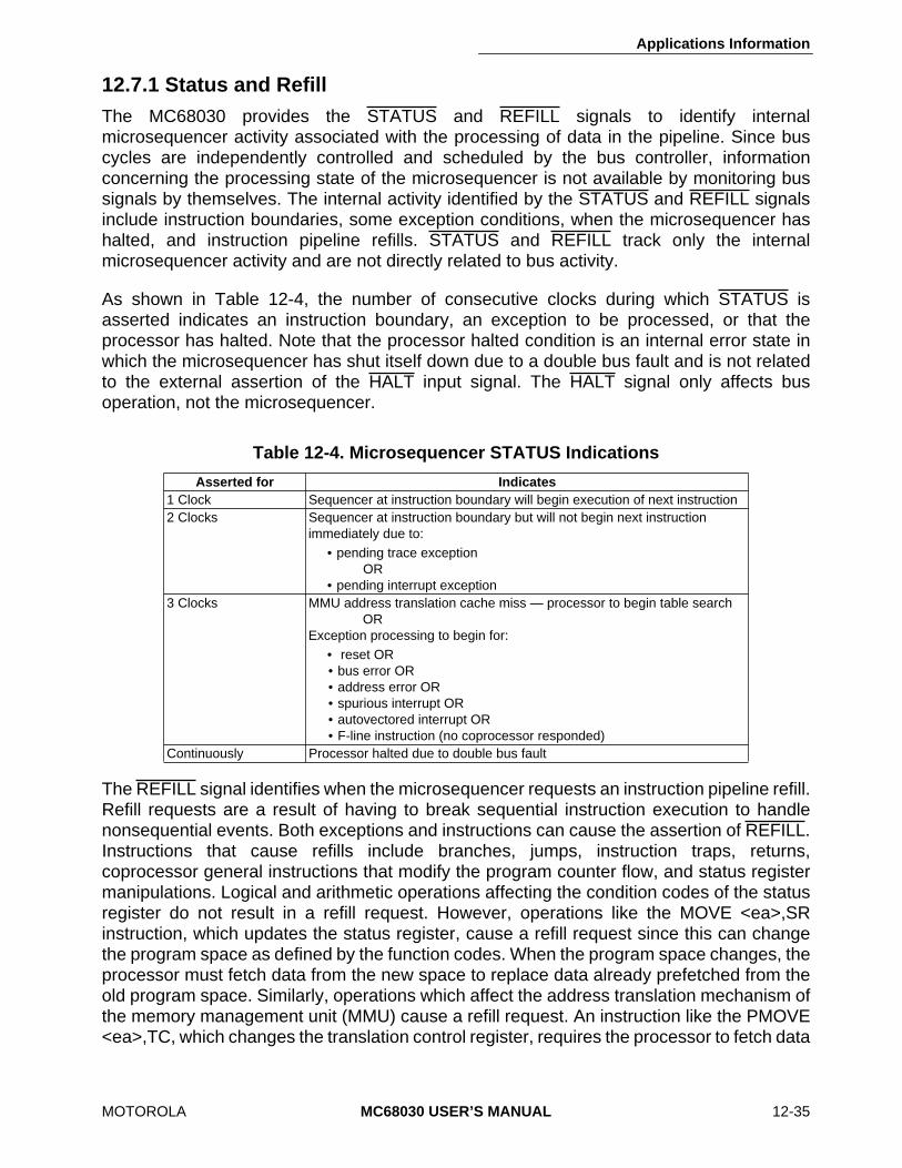
Applications Information
MOTOROLA MC68030 USER’S MANUAL 12-35
12.7.1 Status and RefillThe MC68030 provides the STATUS and REFILL signals to identify internalmicrosequencer activity associated with the processing of data in the pipeline. Since buscycles are independently controlled and scheduled by the bus controller, informationconcerning the processing state of the microsequencer is not available by monitoring bussignals by themselves. The internal activity identified by the STATUS and REFILL signalsinclude instruction boundaries, some exception conditions, when the microsequencer hashalted, and instruction pipeline refills. STATUS and REFILL track only the internalmicrosequencer activity and are not directly related to bus activity.
As shown in Table 12-4, the number of consecutive clocks during which STATUS isasserted indicates an instruction boundary, an exception to be processed, or that theprocessor has halted. Note that the processor halted condition is an internal error state inwhich the microsequencer has shut itself down due to a double bus fault and is not relatedto the external assertion of the HALT input signal. The HALT signal only affects busoperation, not the microsequencer.
The REFILL signal identifies when the microsequencer requests an instruction pipeline refill.Refill requests are a result of having to break sequential instruction execution to handlenonsequential events. Both exceptions and instructions can cause the assertion of REFILL.Instructions that cause refills include branches, jumps, instruction traps, returns,coprocessor general instructions that modify the program counter flow, and status registermanipulations. Logical and arithmetic operations affecting the condition codes of the statusregister do not result in a refill request. However, operations like the MOVE <ea>,SRinstruction, which updates the status register, cause a refill request since this can changethe program space as defined by the function codes. When the program space changes, theprocessor must fetch data from the new space to replace data already prefetched from theold program space. Similarly, operations which affect the address translation mechanism ofthe memory management unit (MMU) cause a refill request. An instruction like the PMOVE<ea>,TC, which changes the translation control register, requires the processor to fetch data
Table 12-4. Microsequencer STATUS Indications
Asserted for Indicates1 Clock Sequencer at instruction boundary will begin execution of next instruction2 Clocks Sequencer at instruction boundary but will not begin next instruction
immediately due to:• pending trace exception
OR• pending interrupt exception
3 Clocks MMU address translation cache miss — processor to begin table searchOR
Exception processing to begin for:• reset OR• bus error OR• address error OR• spurious interrupt OR• autovectored interrupt OR• F-line instruction (no coprocessor responded)
Continuously Processor halted due to double bus fault

Applications Information
12-36 MC68030 USER’S MANUAL MOTOROLA
from the new address translation base. The Test Condition, Decrement, and Branch (DBcc)instruction causes two refill requests when the condition being tested is false. To optimizebranching performance, the DBcc instruction requests a refill before the condition is tested.If the condition is false, another refill is requested to continue with the next sequentialinstruction.
Figure 12-19 illustrates the relation between the CLK signal and normal instructionboundaries as identified by the STATUS signal. STATUS asserting for one clock cycleidentifies normal instruction boundaries. Note that the assertion of REFILL does notnecessarily correspond to the assertion of STATUS. Both STATUS and REFILL assert andnegate from the falling edge of the CLK signal.
Figure 12-20 shows a normal instruction boundary followed by a trace or interrupt exceptionboundary. STATUS asserting for two clock cycles identifies a trace or interrupt exception.Instruction boundary information is still present since both trace and interrupt exceptions areprocessed only at instruction boundaries. Before the exception handler instructions areprefetched, the REFILL signal asserts (not shown) to identify a change in program flow.
(UNABLE TO LOCATE ART)
Figure 12-19. Normal Instruction Boundaries
Applications Information
MOTOROLA MC68030 USER’S MANUAL 12-37
Figure 12-21 illustrates the assertion of the STATUS signal for other exception conditions,which include MMU address translation cache miss, reset, bus error, address error,spurious interrupt, autovectored interrupt, and F-line instruction when no coprocessorresponds. Exception processing causes STATUS to assert for three clock cycles to indicatethat normal instruction processing has stopped. Instruction boundaries cannot bedetermined in this case since these exceptions are processed immediately, not just atinstruction boundaries.
Figure 12-22 shows the assertion of STATUS, indicating that the processor has halted dueto a double bus fault. Once a bus error has occurred, any additional bus error exceptionoccurring before the execution of the first instruction of the bus error handler routineconstitutes a double bus fault. The processor also halts if it receives a bus error or addresserror during the vector table read operations or the prefetch for the first instruction after anexternal reset. STATUS remains asserted until the processor is reset.
(UNABLE TO LOCATE ART)
Figure 12-20. Trace or Interrupt Exception
(UNABLE TO LOCATE ART)
Figure 12-21. Other Exceptions
Applications Information
12-38 MC68030 USER’S MANUAL MOTOROLA
12.7.2 Real-Time Instruction TraceMicroprocessor-based systems used for real-time applications typically lack developmentaids for program debug. The real-time environment does not allow program instructionexecution to arbitrarily stop to handle debugging events. These systems include controlapplications where mechanical events cannot halt, such as robotics, automotive, andindustrial control and emulator systems which may need to keep the target system executingin real time.
To solve the problems inherent with real-time systems, the MC68030 incorporates extrahardware-based features to enhance program debug. Real-time systems cannot takeadvantage of the trace exception mechanism built into all M68000 Family processors sincethis takes processing time away from real-time events. Additional output pins have beenincorporated into the MC68030 to gain real-time visibility into the processor. Tracingcapability can be added by decoding MC68030 control signals to detect which cycles areimportant for tracking. Post analysis of collected data allows for program debug.
Several problems exist with an external trace mechanism. These problems includedetermining which cycles are important for tracking program flow, detecting if instructionsobtained in prefetch operations are discarded by the execution unit, and the inability ofexternal trace circuitry to capture accesses to on-chip cache memories.
External trace hardware used for program debug must be synchronized to the MC68030 busactivity. Since all clock cycles are not traced in a program debug environment, the tracehardware requires a sampling signal. For external read and write operations, trace samplingoccurs when the data bus contains valid data. Two modes of external bus operation arepossible: the synchronous mode in which the system returns the STERM signal and theasynchronous mode in which the system responds with the DSACK1 and/or the DSACK0signals. Both modes of bus operation need to generate a sampling signal when valid datais present on the bus. This allows for tracing data flow in and out of the processor, which isthe basis for tracking program execution.
(UNABLE TO LOCATE ART)
Figure 12-22. Processor Halted

Applications Information
12-39 MC68030 USER’S MANUAL MOTOROLA
The pipelined architecture of the MC68030 prefetches instructions and operands to keep thethree stages of the instruction pipe full. The pipeline allows concurrent operations to occurfor up to three words of a single instruction or for up to three consecutive instructions. Whilesequential instruction execution is the norm, it is possible that prefetched data is not usedby the execution unit due to a nonsequential event. The STATUS signal allows tracehardware to mark the progress of the execution unit as it processes program memoryoperands and allows marking of some exceptions. Nonsequential events, where the entirepipeline needs to reload before continuing execution, are marked by the REFILL signal.
External hardware typically has no visibility into on-chip cache memory operations.However, the MC68030 provides a local address reference to increase visibility. Writeoperations are totally visible since the MC68030 implements a writethrough policy allowingexternal hardware to capture data. For read operations from on-chip cache memories, theleast significant byte of the address bus provides a local address reference.
The MC68030 begins an external cycle by driving the address bus and asserting theexternal cycle start (ECS) signal. Address strobe (AS) asserts later in the cycle to validatethe address. If a hit occurs in the cache or the cache holding register, then the external cycleis aborted and AS is not asserted. In addition, the low-order address bits (A0=A7) are notinvolved in the address translation process performed by the on-chip MMU, creating a localaddress reference which can be used by trace functions. All read cycles from the on-chipcache memories cannot be captured externally since the cache access does not depend onthe availability of the external bus.
Figure 12-23 shows a trace interface circuit which can be used with a logic analyzer forprogram debug. The nine input signals (DSACK1, DSACK0, CLK, AS, RESET, STATUS,REFILL, STERM, and ECS) are connected to the MC68030 processor in the system underdevelopment. Six output signals are generated to aid in capturing and analyzing data. Inaddition to connecting the logic analyzer to the address bus, the data bus, and the buscontrol signals, the trace interface signals (SAMPLE, PHALT, FILL, EP, IE, and ECSC)should also be connected. The external clock probe of the logic analyzer connects to thesystem CLK signal for synchronization. Setting up the logic analyzer for data capturerequires that samples be taken on the falling edge of the CLK signal when the SAMPLEsignal is high. Table 12-5 lists the parts required to implement this circuit.
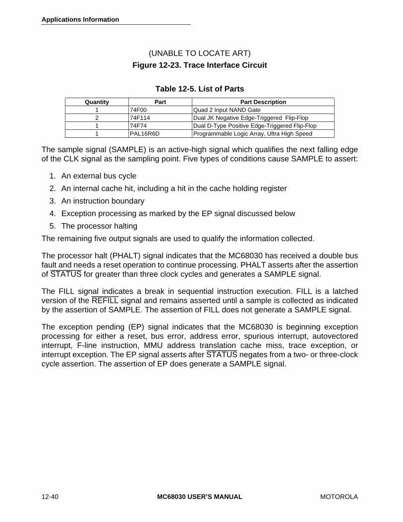
Applications Information
12-40 MC68030 USER’S MANUAL MOTOROLA
The sample signal (SAMPLE) is an active-high signal which qualifies the next falling edgeof the CLK signal as the sampling point. Five types of conditions cause SAMPLE to assert:
1. An external bus cycle
2. An internal cache hit, including a hit in the cache holding register
3. An instruction boundary
4. Exception processing as marked by the EP signal discussed below
5. The processor halting
The remaining five output signals are used to qualify the information collected.
The processor halt (PHALT) signal indicates that the MC68030 has received a double busfault and needs a reset operation to continue processing. PHALT asserts after the assertionof STATUS for greater than three clock cycles and generates a SAMPLE signal.
The FILL signal indicates a break in sequential instruction execution. FILL is a latchedversion of the REFILL signal and remains asserted until a sample is collected as indicatedby the assertion of SAMPLE. The assertion of FILL does not generate a SAMPLE signal.
The exception pending (EP) signal indicates that the MC68030 is beginning exceptionprocessing for either a reset, bus error, address error, spurious interrupt, autovectoredinterrupt, F-line instruction, MMU address translation cache miss, trace exception, orinterrupt exception. The EP signal asserts after STATUS negates from a two- or three-clockcycle assertion. The assertion of EP does generate a SAMPLE signal.
(UNABLE TO LOCATE ART)
Figure 12-23. Trace Interface Circuit
Table 12-5. List of Parts
Quantity Part Part Description1 74F00 Quad 2 Input NAND Gate2 74F114 Dual JK Negative Edge-Triggered Flip-Flop1 74F74 Dual D-Type Positive Edge-Triggered Flip-Flop1 PAL16R6D Programmable Logic Array, Ultra High Speed

Applications Information
12-41 MC68030 USER’S MANUAL MOTOROLA
The instruction executed (IE) signal indicates the execution unit has just finished processingan instruction. The IE signal asserts after STATUS negates from a one-clock cycleassertion. The assertion of IE also generates a SAMPLE signal.
The external cycle start condition (ECSC) signal is used in conjunction with the AS signal todetermine if the address bus and data bus are valid in the current trace sample. Table 12-6 lists the possible combinations of AS and ECSC and shows what parts of the tracedaddress and data bus are valid. The assertion of ECSC does not generate a SAMPLEsignal.
Figure 12-24 shows the pin definitions for the PAL16R6 package used in the trace circuit.These definitions are used by the PAL equations listed in Figure 12-25.
12.8 POWER AND GROUND CONSIDERATIONSThe MC68030 is fabricated in Motorola's advanced HCMOS process, containsapproximately 275,000 total transistor sites, and is capable of operating at clock frequenciesof up to 33.33 MHz. While the use of CMOS for a device containing such a large number oftransistors allows significantly reduced power consumption in comparison to an equivalentNMOS circuit, the high clock speed makes the characteristics of power supplied to thedevice very important. The power supply must be able to supply large amounts ofinstantaneous current when the MC68030 performs certain operations, and it must remainwithin the rated specification at all times. To meet these requirements, more detailedattention must be given to the power supply connection to the MC68030 than is required forNMOS devices that operate at slower clock rates.
Table 12-6. AS and ECSC Indicates
AS ECSC Indicates0 0 Both Address and Data Bus Are Valid0 1 Both Address and Data Bus Are Valid1 0 Address Bits (A0=A7) are Valid
Address Bits (A8=A31) Are InvalidData Bus Is Invalid
1 1 Both Address and Data Bus Are Invalid

Applications Information
12-42 MC68030 USER’S MANUAL MOTOROLA
To supply a solid power supply interface, 10 VCC pins and 14 GND pins are provided. Thisallows two VCC and four GND pins to supply power for the address bus and two VCC andfour GND pins to supply the data bus; the remaining VCC and GND pins are used by theinternal logic and clock generation circuitry. Table 12-7 lists the VCC and GND pinassignments.
To reduce the amount of noise in the power supplied to the MC68030 and to provide forinstantaneous current requirements, common capacitive decoupling techniques should beobserved. While there is no recommended layout for this capacitive decoupling, it isessential that the inductance between these devices and the MC68030 be minimized toprovide sufficiently fast response time to satisfy momentary current demands and tomaintain a constant supply voltage. It is suggested that a combination of low, middle, andhigh frequency, high-quality capacitors be placed as close to the MC68030 as possible (e.g.,a set of 10 µF, 0.1 µF, and 330 pF capacitors in parallel provides filtering for mostfrequencies prevalent in a digital system). Similar decoupling techniques should also beobserved for other VLSI devices in the system.
(UNABLE TO LOCATE ART)
Figure 12-24. PAL Pin Definition

Applications Information
12-43 MC68030 USER’S MANUAL MOTOROLA
In addition to the capacitive decoupling of the power supply, care must be taken to ensurea low-impedance connection between all MC68030 VCC and GND pins and the systempower supply planes. Failure to provide connections of sufficient quality between theMC68030 power supply pins and the system supplies will result in increased assertiondelays for external signals, decreased voltage noise margins, and potential errors in internallogic.
(UNABLE TO LOCATE ART)
Figure 12-25. Logic Equations
Table 12-7. VCC and GND Pin Assignments
Pin Group VCC GND
Address Bus C6, D10 C5, C7, C9, E11
Data Bus L6, K10 J11, L9, L7, L5
ECS, SIZx, DS, AS, DBEN, CBREQ, R/W K4 J3
FC0=FC2, RMC, OCS, CIOUT, BG D4 E3
Internal Logic, RESET, STATUS, REFILL, Misc. H3, F2, F11, H11 L8, G3, F3, G11
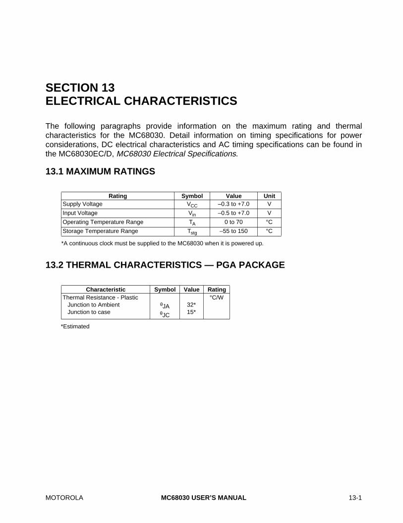
MOTOROLA
MC68030 USER’S MANUAL
13-1
SECTION 13ELECTRICAL CHARACTERISTICS
The following paragraphs provide information on the maximum rating and thermalcharacteristics for the MC68030. Detail information on timing specifications for powerconsiderations, DC electrical characteristics and AC timing specifications can be found inthe MC68030EC/D,
MC68030 Electrical Specifications
.
13.1 MAXIMUM RATINGS
*A continuous clock must be supplied to the MC68030 when it is powered up.
13.2 THERMAL CHARACTERISTICS — PGA PACKAGE
*Estimated
Rating Symbol Value Unit
Supply Voltage V
CC
–0.3 to +7.0 V
Input Voltage V
in
–0.5 to +7.0 V
Operating Temperature Range T
A
0 to 70
°
C
Storage Temperature Range T
stg
–55 to 150
°
C
Characteristic Symbol Value Rating
Thermal Resistance - PlasticJunction to Ambient Junction to case
θ
JA
θ
JC
32*15*
°
C/W

MOTOROLA
MC68030 USER’S MANUAL
14-1
SECTION 14ORDERING INFORMATION AND MECHANICAL DATA
This section contains the pin assignments and package dimensions of the MC68030. Inaddition, detailed information is provided to be used as a guide when ordering.
14.1 STANDARD MC68030 ORDERING INFORMATION
Package TypeFrequency
(MHz)Temperature Order Number
Pin Grid Array RC Suffix
20.025.033.33
0
°
C to 70
°
C0
°
C to 70
°
C0
°
C to 70
°
C
MC68030RC20MC68030RC25MC68030RC33
Ceramic Surface Mount FE Suffix
20.025.033.33
0
°
C to 70
°
C0
°
C to 70
°
C0
°
C to 70
°
C
MC68030FE20MC68030FE25MC68030FE33

Ordering Information and Mechanical Data
14-2
MC68030 USER’S MANUAL
MOTOROLA
14.2 PIN ASSIGNMENTS — PIN GRID ARRAY (RC SUFFIX)
The V
CC
and GND pins are separated into three groups to provide individual power supplyconnections for the address bus buffers, data bus buffers, and all other output buffers andinternal logic.
14.3 PIN ASSIGNMENTS — CERAMIC SURFACE MOUNT (FE SUFFIX)
Pin Group V
CC
GND
Address Bus C6, D10 C5, C7, C9, E11
Data Bus L6, K10 J11, L9, L7, L5
ECS, SIZx, DS, AS, DBEN, CBREQ, R/W K4 J3
FC0-FC2, RMC, OCS, CIOUT, BG D4 E3
Internal Logic, RESET, STATUS, REFILL, Misc. H3, F2, F11, H11 L8, G3, F3, G11
(UNABLE TO LOCATE ART)
(UNABLE TO LOCATE ART)
Ordering Information and Mechanical Data
MOTOROLA
MC68030 USER’S MANUAL
14-3
14.4 PACKAGE DIMENSIONS
MC68030
RC Suffix Package Case 789C-01
(UNABLE TO LOCATE ART)

Ordering Information and Mechanical Data
14-4
MC68030 USER’S MANUAL
MOTOROLA
MC68030
FE Suffix Package Case 831-01
(UNABLE TO LOCATE ART)
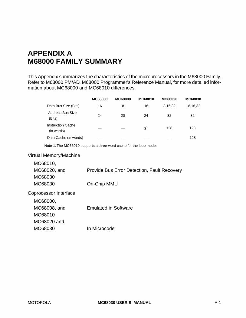
MOTOROLA
MC68030 USER’S MANUAL
A-1
APPENDIX AM68000 FAMILY SUMMARY
This Appendix summarizes the characteristics of the microprocessors in the M68000 Family.Refer to M68000 PM/AD, M68000 Programmer's Reference Manual, for more detailed infor-mation about MC68000 and MC68010 differences.
Note 1. The MC68010 supports a three-word cache for the loop mode.
Virtual Memory/Machine
MC68010,MC68020, and Provide Bus Error Detection, Fault RecoveryMC68030MC68030 On-Chip MMU
Coprocessor Interface
MC68000,MC68008, and Emulated in SoftwareMC68010MC68020 andMC68030 In Microcode
MC68000 MC68008 MC68010 MC68020 MC68030
Data Bus Size (Bits) 16 8 16 8,16,32 8,16,32
Address Bus Size
(Bits)24 20 24 32 32
Instruction Cache
(in words)— — 3
1
128 128
Data Cache (in words) — — — — 128
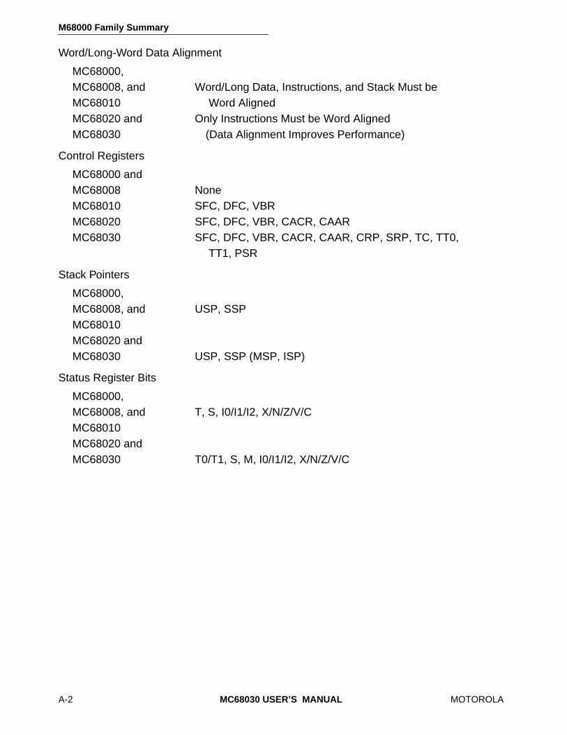
M68000 Family Summary
A-2
MC68030 USER’S MANUAL
MOTOROLA
Word/Long-Word Data Alignment
MC68000,MC68008, and Word/Long Data, Instructions, and Stack Must beMC68010 Word AlignedMC68020 and Only Instructions Must be Word AlignedMC68030 (Data Alignment Improves Performance)
Control Registers
MC68000 andMC68008 NoneMC68010 SFC, DFC, VBRMC68020 SFC, DFC, VBR, CACR, CAARMC68030 SFC, DFC, VBR, CACR, CAAR, CRP, SRP, TC, TT0,
TT1, PSR
Stack Pointers
MC68000,MC68008, and USP, SSPMC68010MC68020 andMC68030 USP, SSP (MSP, ISP)
Status Register Bits
MC68000,MC68008, and T, S, I0/I1/I2, X/N/Z/V/CMC68010MC68020 andMC68030 T0/T1, S, M, I0/I1/I2, X/N/Z/V/C

M68000 Family Summary
MOTOROLA
MC68030 USER’S MANUAL
A-3
Function Code/Address Space
MC68000 andMC68008 FC0–FC2=7 is Interrupt Acknowledge OnlyMC68010,MC68020, and FC0–FC2=7 is CPU SpaceMC68030
Indivisible Bus Cycles
MC68000,MC68008, and Use AS SignalMC68010MC68020 andMC68030 Use RMC Signal
Stack Frames
MC68000 andMC68008 Support Original SetMC68010 Supports Formats $0, $8MC68020 andMC68030 Support Formats $0, $1, $2, $9, $A, $B
Addressing Modes
MC68020 and Memory indirect addressing modes, scaled index,MC68030 extensions: and larger displacements. Refer to specific data
sheets for details.
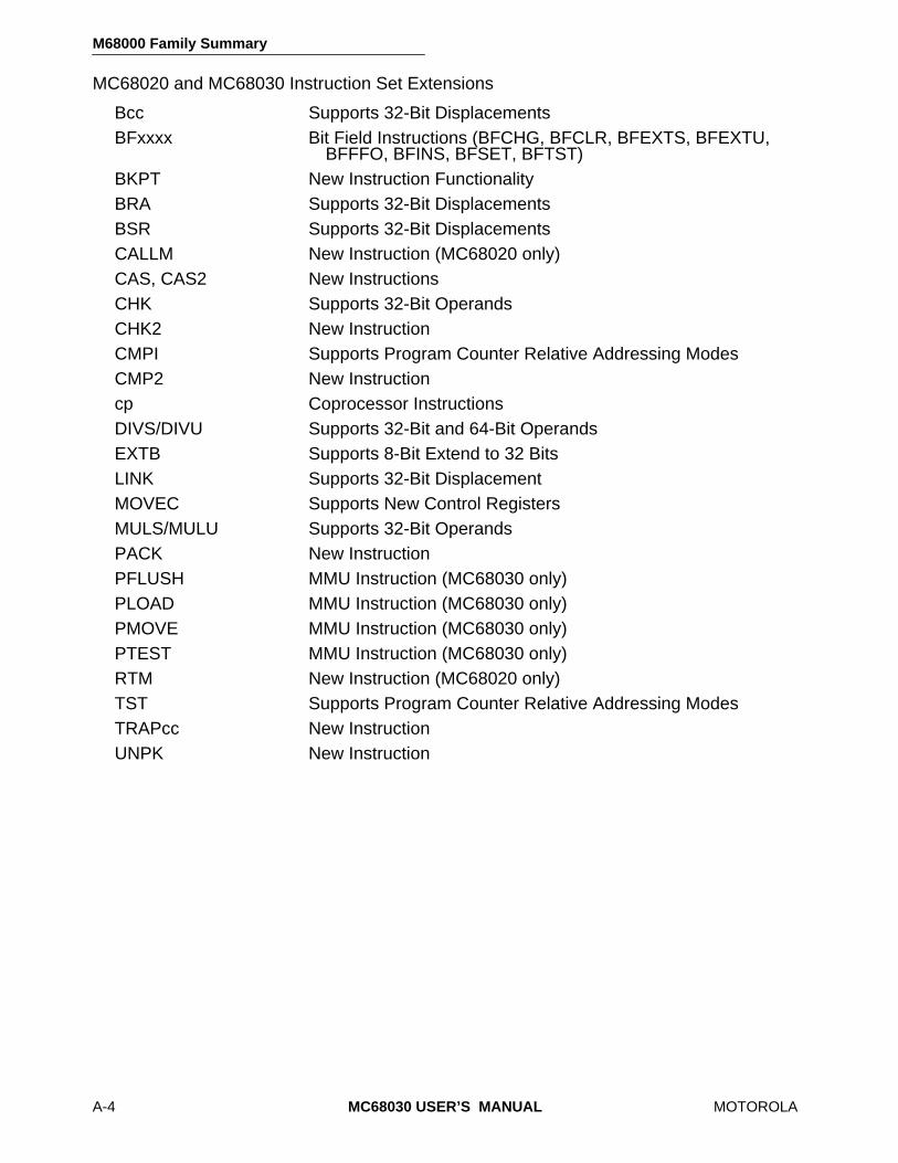
M68000 Family Summary
A-4
MC68030 USER’S MANUAL
MOTOROLA
MC68020 and MC68030 Instruction Set Extensions
Bcc Supports 32-Bit DisplacementsBFxxxx Bit Field Instructions (BFCHG, BFCLR, BFEXTS, BFEXTU,
BFFFO, BFINS, BFSET, BFTST)BKPT New Instruction FunctionalityBRA Supports 32-Bit DisplacementsBSR Supports 32-Bit DisplacementsCALLM New Instruction (MC68020 only)CAS, CAS2 New InstructionsCHK Supports 32-Bit OperandsCHK2 New InstructionCMPI Supports Program Counter Relative Addressing ModesCMP2 New Instructioncp Coprocessor InstructionsDIVS/DIVU Supports 32-Bit and 64-Bit OperandsEXTB Supports 8-Bit Extend to 32 BitsLINK Supports 32-Bit DisplacementMOVEC Supports New Control RegistersMULS/MULU Supports 32-Bit OperandsPACK New InstructionPFLUSH MMU Instruction (MC68030 only)PLOAD MMU Instruction (MC68030 only)PMOVE MMU Instruction (MC68030 only)PTEST MMU Instruction (MC68030 only)RTM New Instruction (MC68020 only)TST Supports Program Counter Relative Addressing ModesTRAPcc New InstructionUNPK New Instruction

MOTOROLA
MC68030 USER’S MANUAL
Index-1
INDEX
A
Abort Task Routine 9-82Absolute Long Address Mode 2-20Absolute Short Address Mode 2-20Access Time Calculations, Memory 12-14Accesses, Read-Modify-Write 6-10Acknowledge, Breakpoint 8-10Activity
Data Bus 12-11Processor
Even Alignment 11-9Odd Alignment 11-10
Actual Instruction Cache Case 11-11Adapter Board
MC68020 12-1Signal Routing 12-2
Address Bus 5-4, 7-4, 7-30, 12-4Address Encoding, CPU Space 7-69Address Error Exception 8-8, 10-72Address Offset Encoding 7-8Address Register
Direct Mode 2-10Indirect Displacement Mode 2-12Indirect Index (Base Displacement)
Mode 2-13Indirect Index (8-Bit Displacement) Mode
2-12Indirect Mode 2-10Indirect Postincrement Mode 2-10Indirect Predecrement Mode 2-11
Address Registers 1-6, 2-4Address Space Types 4-5Address Strobe Signal 5-5, 7-3–7-4, 7-26Address Translation 9-13
Cache 7-3, 9-4, 9-17Cache Entry 9-18General Flowchart 9-13
AddressingCapabilities 2-25Compatibility, M68000 2-36Indexed 2-26Indirect 2-28Indirect Absolute Memory 2-28Mode Summary 2-31
Modes 1-10, 2-8Structure 2-36
Aids, Debugging 12-35Arbitration, Bus 7-96Arithmetic/Logical Instruction
Immediate, Timing Table 11-42Timing Table 11-40
AS Signal 5-5, 7-3–7-4, 7-26Assignments, Exception Vector 8-2Assignment, Pin 14-2–14-3Asynchronous
Bus Operation 7-27Byte
Read Cycle Flowchart 7-31Read Cycle, 32-Bit Port, Timing 7-31Read-Modify-Write Cycle, 32-Bit
Port, Timing 7-43Write Cycle, 32-Bit Port, Timing 7-37
Cycle Signal Assertion Results 7-78Long-Word Read Cycle Flowchart 7-31Read Cycle 7-31
32-Bit Port, Timing 7-31Read-Modify-Write Cycle 7-43
Flowchart 7-43Sample Window 7-3Word
Read Cycle, 32-Bit Port, Timing 7-31Write Cycle, 32-Bit Port, Timing 7-37
Write Cycle 7-37Flowchart 7-3732-8it Port, Timing 7-37
ATC 7-3, 9-4, 9-17Entry 9-17
Creation Flowchart 9-42Autovector Interrupt Acknowledge Cycle 7-71
Timing 7-71Autovector Signal 5-8, 7-6, 7-29, 7-71, 8-20AVEC Signal 5-8, 7-6, 7-29, 7-71, 8-20Average No Cache Case 11-8A0-A1 Signals 7-8, 7-22A0-A31 Signals 5-4, 7-4, 7-31A0-A7 1-6
Index
Index
-2
MC68030 USER’S MANUAL
MOTOROLA
B
BERR Signal 5-9, 6-11, 7-6, 7-27, 8-7, 8-22, 8-25
Best Case 11-7BG Signal 5-9, 7-43, 7-95–7-96BGACK Signal 5-9, 7-97Binary-Coded Decimal Instruction Timing
Table 11-43Binary-Coded Decimal Instructions 3-10Bit
CA 10-35CD 6-21CED 6-21CEI 6-22CI 6-22Clear Data Cache 6-21Clear Entry in Data Cache 6-21Clear Entry in Instruction Cache 6-22Clear Instruction Cache 6-22Data Burst Enable 6-21DBE 6-21DR 10-36ED 6-22EI 6-23Enable Data Cache 6-22Enable Instruction Cache 6-23FD 6-22FI 6-23Freeze Data Cache 6-22Freeze Instruction Cache 6-23IBE 6-22Instruction Burst Enable 6-22PC 10-35WA 6-21Write Allocate 6-21
Bit FieldInstruction Timing Table 11-47Instructions 3-9Operations 3-31
Bit ManipulationInstruction Timing Table 11-46Instructions 3-8
BKPT Instruction 7-74, 8-12, 8-22Block Diagram 1-2, 9-2
MMU 9-2Processor Resource 11-3
BR Signal 5-8, 7-43, 7-60, 7-96
Branch on Coprocessor Condition Instruction 10-13
Breakpoint Acknowledge 8-10Cycle 7-74
Exception Signaled, Timing 7-74Timing 7-74
Flowchart 7-74Breakpoint Instruction 7-74, 8-22
Exception 8-22Buffer
Instruction Fetch Pending 11-5Write Pending 11-5
BurstCycle 7-59, 12-17Mode
Cache Filling 6-10Static RAM 12-24
Operation 7-59Flowchart 7-61
BusAddress 5-4, 7-3, 7-30, 12-4Arbitration 7-96
Bus Inactive, Timing 7-103Control 7-100Flowchart 7-97Latency 11-62State Diagram 7-100Timing 7-97
Control Signals 7-3Controller 11-4Data 5-4, 7-5, 7-30, 12-9, 12-24Error
Exception 8-7, 10-72Late, STERM, Timing 7-83Late, Third Access, Timing 7-86Late, With DSACKx, Timing 7-83Second Access, Timing 7-86Signal 5-9, 6-11, 7-6, 7-27, 8-7, 8-22Without DSACKx Timing 7-83
Errors 7-82Exceptions 7-75Fault Recovery 8-27Operation
Asynchronous 7-27Synchronous 7-28–7-29
Synchronization 7-95Timing 7-96
Transfer Signals 7-1

Index
MOTOROLA
MC68030 USER’S MANUAL
Index-3
Bus Grant 7-99Signal 5-9, 7-43, 7-96
Bus Grant Acknowledge 7-100Signal 5-9, 7-97
Bus Request 7-98Signal 5-8, 7-43, 7-60, 7-96
Busy Primitive 10-36Byte
Data Select 7-23Read Cycle, Asynchronous
Flowchart 7-3132-Bit Port, Timing 7-31
Select Logic 12-9Write Cycle, Asynchronous, 32-Bit Port,
Timing 7-37
C
CA Bit 10-35CAAR 1-9, 2-5, 6-23Cache
Address Translation 7-3, 9-4, 9-17Data 1-16, 6-6, 11-4, 11-16External 12-32Filling 7-24
Burst Mode 6-15Single Entry 6-10
Instruction 1-16, 6-1, 6-4, 11-4Interactions 7-26Organization 6-1Reset 6-20
Cache Address Register 1-9, 2-5, 6-23Cache Burst Acknowledge Signal 5-7, 6-16,
7-24, 7-30Cache Burst Request Signal 5-7, 6-16, 7-6,
7-30, 7-48Cache Control Register 1-9, 2-5, 6-3–6-4,
6-20–6-21Cache Disable Signal 5-10, 6-3Cache Inhibit Input Signal 5-7, 6-3, 6-9, 6-15,
7-3, 7-26Cache Inhibit Output Signal 5-7, 6-3, 6-9,
7-30, 9-2, 9-13CACR 1-5, 2-5, 6-3–6-4, 6-20Calculate Effective Address Timing Table
11-30Calculate Immediate Effective Address
Timing
Table 11-32Calculations, Execution Time 11-6Capabilities, Addressing 2-25CAS Instruction 7-43
Example 3-25Case
Actual Instruction Cache 11-11Average No Cache 11-8Best 11-7Instruction Cache 11-6
CAS2 Instruction 7-43Example 3-26
CBACK Signal 5-7, 6-16, 7-24, 7-30CBREQ Signal 5-7, 6-16, 7-6, 7-30, 7-48CCR 2-4, 3-14CD Bit 6-21CDIS Signal 5-10, 6-3CED Bit 6-21CEI Bit 6-22Changing Privilege Level 4-4CI Bit 6-22CIIN Signal 5-7, 6-3, 6-9, 6-15, 7-3, 7-26CIOUT Signal 5-7, 6-3, 6-9, 7-30, 9-2, 9-17CIR 10-8, 10-29
Command 10-31Condition 10-31Control 10-30Instruction Address 10-33Operand 10-32Operand Address 10-33Operation Word 10-31Register Select 10-32Response 10-29Restore 10-31Save 10-30
Clear Data Cache Bit 6-21Clear Entry in Data Cache Bit 6-21Clear Entry in Instruction Cache Bit 6-22Clear Instruction Cache Bit 6-22CLK Signal 5-11, 7-54Clock Signal 5-11, 7-54Command CIR 10-31Command Words, Illegal, Coprocessor
Detected 10-63Compare and Swap Instruction 7-43Compatibility, M68000 Addressing 2-36Computation, Condition Code 3-15Concurrent Operation 10-3

Index
Index
-4
MC68030 USER’S MANUAL
MOTOROLA
Condition CIR 10-31Condition Code
Computation 3-15Register 2-4, 3-14
Condition Tests 3-17Conditional Branch Instruction Timing Table
11-48Connections, Power Supply 5-11Considerations
Ground 12-43Power 12-43
Contiguous Memory 9-33–9-34Example 9-34
ControlBus Arbitration 7-100Early Termination 12-34
Control CIR 10-30Control Instruction Timing Table 11-49Controller
Bus 11-4Micro Bus 11-5
CoprocessorCommunication Cycle 7-74Conditional Instructions 10-12Context Restore Instruction 10-27Context Save Instruction 10-24Data Processing Exceptions 10-63DMA 10-6Format Words 10-22General Instruction Protocol 10-11General Instructions 10-9Identification Code 10-4Instruction Format 10-4Instruction Summary 10-72Instructions 3-21Interface 10-1, 10-6MC68881 12-5MC68882 12-5Non-DMA 10-6Reset 10-72Response Primitive 10-33Response Primitive Format 10-35State Frames 10-20–10-21System Related Exceptions 10-64
Coprocessor DetectedExceptions 10-61Format Errors 10-64Illegal Command Words 10-63
Illegal Condition Words 10-63Protocol Violations 10-62
Coprocessor Interface Register 10-8, 10-29Count, Initial Shift 9-69cpBcc Instruction 10-14cpDBcc Instruction 10-17CpID 7-74, 10-4cpRESTORE Instruction 10-27cpSAVE Instruction 10-25cpScc Instruction 10-15cpTRAPcc Instruction 10-18cpTRAPcc Instruction Exception 10-69CPU Root Pointer 1-9, 2-5, 9-23, 9-52, 9-54,
9-65CPU Space 7-68, 7-70, 10-7CPU Space Address Encoding 7-69CRP 1-9, 2-5, 9-23, 9-52, 9-54, 9-65Cycle
Asynchronous Read 7-31Breakpoint Acknowledge 7-74Burst 7-59, 12-17Coprocessor Communication 7-74Interrupt Acknowledge 7-69Interrupt Acknowledge, Autovector 7-71
Cycles, Data Transfer 7-30
D
DataBus 5-4, 7-5, 7-30, 12-9
Activity 12-11Requirements, Read Cycle 7-9Write Enable Signals 7-22
Cache 1-16, 6-1, 6-6, 11-4, 11-16Movement Instructions 3-4Port Organization 7-8Register Direct Mode 2-9Registers 1-6, 2-2Select, Byte 7-23Transfer
Cycles 7-30Transfer Mechanism 7-6
Types 1-10Data Buffer Enable Signal 5-6, 7-5, 7-31Data Burst Enable Bit 6-21Data Strobe Signal 5-6, 7-5, 7-27Data Transfer and Size Acknowledge Signals
5-6, 6-11, 6-14, 7-5–7-6, 7-26

Index
MOTOROLA
MC68030 USER’S MANUAL
Index-5
Data, Immediate 2-21DBE Bit 6-21DBEN Signal 5-6, 7-5, 7-31Debugging Aids 12-35Decoding, MMU Status Register 9-61Definition, Task Memory Map 9-66Delay, Input 7-2Derivation, Table Index 9-9Description, General 1-1Descriptor
Bits, Unused 9-71Fetch Operation Flowchart 9-44Indirect
Long Format 9-28Short Format 9-27
InvalidLong Format 9-28Short Format 9-26
PageLong Format 9-26Short Format 9-26
Page, Early TerminationLong Format 9-25Short Format 9-25
Root Pointer 9-23Table
Long Format 9-24Short Format 9-24
Descriptors, Translation Table 9-10, 9-20DFC 1-8, 2-2, 2-5Differences
MC68020 Hardware 12-3MC68020 Software 12-4MMU 9-51
DMA Coprocessor 10-5Double Bus Fault 7-94, 8-7Doubly-Linked List
Deletion Example 3-28Insertion Example 3-28
DR Bit 10-36DS Signal 5-6, 7-5, 7-27DSACK0 Signal 5-6, 6-11, 6-14, 7-5–7-6,
7-26DSACK1 Signal 5-6, 6-11, 6-14, 7-5–7-6,
7-26Dynamic Allocation, Table 9-40Dynamic Bus Sizing 7-6, 7-19, 7-24D0-D31 Signals 5-4, 7-5, 7-30
D0-D7 1-6
E
Early Termination 9-25, 9-70Early Termination Control 12-34ECS Signal 5-5, 7-3, 7-26ED Bit 6-22Effective Address Encoding Summary 2-22EI Bit 6-23Empty/Reset Format Word 10-22Enable Data Cache Bit 6-22Enable Instruction Cache Bit 6-23Encoding
Address Offset 7-8Size Signal 7-9
Entry, Address Translation Cache 9-17Errors, Bus 7-82EU 6-16Example
CAS Instruction 3-25CAS2 Instruction 3-26Contiguous Memory 9-34Doubly-Linked List
Deletion 3-28Insertion 3-28
Function Code Lookup 9-46Indirection 9-34Linked List
Deletion 3-27Insertion 3-26
Protection, Translation Tree 9-50System Paging Implementation 9-72Table Paging 9-37Table Sharing 9-34Two Task Translation Tree 9-47
ExceptionAddress Error 8-8, 10-72Breakpoint Instruction 8-22Bus Error 8-7, 10-72cpTRAPcc Instruction 10-69Format Error 8-14Illegal Instruction 8-9Instruction Trap 8-9Interrupt 8-14, 10-71MMU Configuration 8-21, 9-62Priority 8-16Privilege Violation 8-11, 10-69
Index
Index
-6
MC68030 USER’S MANUAL
MOTOROLA
Processing 4-6Sequence 8-1State 4-1
Reset 8-2, 8-5Return from 8-24Stack Frame 4-6, 8-32Trace 8-12, 10-70Unimplemented Instruction 8-9Vector
Assignments 8-2Numbers 8-1
Vectors 4-6Exception Related
Instruction Timing Table 11-50Operation Timing Table 11-50
ExceptionsBus 7-75Coprocessor Data Processing 10-63Coprocessor Detected 10-62Coprocessor System Related 10-64F-Line Emulator 8-10, 10-68Multiple 8-23Primitive Processing 10-66
Execution Time Calculations 11-6Execution Unit 6-16Extended Instruction Timing Table 11-43External Cache 12-32
Implementation 12-32Instruction Only 12-35
External Cycle Start Signal 5-5, 7-3, 7-26
F
Fault, Double Bus 7-94, 8-7FC0-FC2 Signals 5-4, 6-6, 7-4, 7-31FD Bit 6-22Fetch Effective Address Timing Table 11-26Fetch Immediate Effective Address Timing
Table 11-28FI Bit 6-23Fields, Limit 9-70F-Line 10-4
Emulator Exceptions 8-10, 10-68Floating Point Units 12-5Flowchart
Address Translation, General 9-13Asynchronous Byte Read Cycle 7-31Asynchronous Long Word Read Cycle
7-31Asynchronous Read-Modify-Write Cycle
7-43Asynchronous Write Cycle 7-37ATC Entry Creation 9-42Breakpoint Acknowledge 7-74Burst Operation 7-61Bus Arbitration 7-97Descriptor Fetch Operation 9-44Interrupt Acknowledge Cycle 7-70Limit Check Procedure 9-43Synchronous Long-Word Read Cycle
7-48Synchronous Read-Modify-Write Cycle
7-54Table Search
Detailed 9-41Initialization 9-42Simplified 9-28
FormatCoprocessor Instruction 10-4Coprocessor Response Primitive 10-35Instruction 3-1Instruction Description 3-18
Format Error Exception 8-14Format Errors
Coprocessor Detected 10-61Main Processor Detected 10-71
Format WordEmpty/Reset 10-22Invalid 10-23Not Ready 10-23Valid 10-24
Format Words, Coprocessor 10-22Formula, Instruction Cache Case Time 11-11Freeze Data Cache Bit 6-22Freeze Instruction Cache Bit 6-23Function Code Lookup 9-45–9-46
Example 9-46Logical Address Map 9-46
Function Code Registers 1-8, 2-5Function Code Signals 5-4, 6-6, 7-4, 7-31
G
General Description 1-1GetFrame Routine 9-74GND Pin Assignments 12-46
Index
MOTOROLA
MC68030 USER’S MANUAL
Index-7
Grant, Bus 7-99Ground Considerations 12-43Groups, Signal 5-1
H
Halt Operation 7-91Timing 7-92
HALT Signal 5-9, 7-6, 7-27Halt Signal 5-9, 7-6, 7-27Halted State 4-1
I
IBE Bit 6-22Identification Code, Coprocessor 10-4Illegal Instruction Exception 8-9Immediate Data 2-21Indexed Addressing 2-26Index, Signal 5-2Indirect Absolute Memory Addressing 2-29Indirect Addressing 2-29Indirection 9-34
Example 9-34Information, Ordering 14-1Initial Reset Timing 7-103Initial Shift Count 9-69Input Delay 7-2Instruction
BKPT 8-22Branch on Coprocessor Condition 10-13Breakpoint 7-74, 8-22CAS 7-43CAS2 7-43Compare and Swap 7-43Coprocessor Context Restore 10-27Coprocessor Context Save 10-24cpBcc 10-14cpDBcc 10-17cpRESTORE 10-27cpSAVE 10-25cpScc 10-15cpTRAPcc 10-18Move Address Space 7-74MOVES 7-74No Operation 7-95NOP 7-95Set on Coprocessor Condition 10-15STOP 8-14
TAS 7-43Test and Set 7-43Test Coprocessor Condition, Decrement
andBranch 10-17
Trap on Coprocessor Condition 10-18Instruction Address CIR 10-33Instruction Boundary Signals 12-37Instruction Burst Enable Bit 6-22Instruction Cache 1-16, 6-1, 6-4, 11-4
Case 11-6Instruction Description
Format 3-18Notation 3-3
Instruction Fetch Pending Buffer 11-5Instruction Format 3-1
Summary 3-18Instruction Set 1-13Instruction Timing Tables 11-24Instruction Trace, Real-Time 12-39Instruction Trap Exception 8-9Instructions
Binary Coded Decimal 3-10Bit Field 3-9Bit Manipulation 3-8Coprocessor 3-21
Conditional 10-12General 10-9
Data Movement 3-4Integer Arithmetic 3-5Logical 3-6MMU 3-13, 9-62Multiprocessor 3-13Privileged 8-11Program Control 3-11Rotate 3-7Shift 3-7System Control 3-12
Integer Arithmetic Instructions 3-5Interactions, Cache 7-26Interface
Coprocessor 10-1, 10-5Memory 12-11
Internal Microsequencer Status Signal 5-10, 7-94
Internal Operand Representation 7-7Internal to External Data Bus Multiplexer 7-10Interrupt

Index
Index
-8
MC68030 USER’S MANUAL
MOTOROLA
Cycle, Spurious 7-74Exception 8-14, 10-71Latency 11-61Levels 8-16
Interrupt Acknowledge Cycle 7-69Flowchart 7-70Timing 7-71
Interrupt Pending Signal 5-8, 8-17–8-18Interrupt Priority Level Signals 5-8, 7-69, 8-15Invalid Format Word 10-23IPEND_Signal 5-8, 8-17–8-18IPL0-IPL2 Signals 5-8, 7-69, 8-15
J
Jump Effective Address Timing Table 11-35
L
Late Bus ErrorSTERM, Timing 7-83Third Access, Timing 7-86With DSACKx, Timing 7-83
Late Retry Operation, Burst, Timing 7-89Latency
Bus Arbitration 11-62Interrupt 11-61
Levels, Interrupt 8-16Limit Check Procedure Flowchart 9-43Limit Fields 9-70Linked List
Deletion Example 3-27Insertion Example 3-26
Logical Address MapFunction Code Lookup 9-45Shared Supervisor/User Address Space
9-46Logical Instructions 3-6Logic, Byte Select 12-9Long Format
Early Termination Page Descriptor 9-25Indirect Descriptor 9-28Invalid Descriptor 9-28Page Descriptor 9-26Table Descriptor 9-24
Long-Word Operand RequestBurst Fill Deferred, Timing 7-61Burst Request
CBACK Negated, Timing 7-61
Wait States, Timing 7-61Burst, CBACK and CIIN Asserted, Timing
7-61Long-Word Read Cycle
Asynchronous, Flowchart 7-31Synchronous, Flowchart 7-4816-Bit Port, Timing 7-3132-Bit Port, Timing 7-318-Bit Port, CIOUT Asserted, Timing 7-31
Long-Word to Long-Word TransferMisaligned 7-19
Cachable 7-19Long-Word to Word Transfer 7-10
Misaligned 7-15Long-Word Write Cycle
16-Bit Port, Timing 7-378-Bit Port, Timing 7-37
Lookup, Function Code 9-45–9-46
M
Machine, Virtual 1-14Main Processor Detected
Format Errors 10-71Protocol Violations 10-67
MC68020Adapter Board 12-1Hardware Differences 12-3Software Differences 12-4
MC68851 Signals 12-4MC68881 Coprocessor 12-6MC68882 Coprocessor 12-6Mechanism, Data Transfer 7-6Memory
Contiguous 9-33–9-34Interface 12-11Virtual 1-12, 9-76
Memory Access Time Calculations 12-14Memory Data Organization 2-5Memory Indirect Postindexed Mode 2-14Memory Indirect Preindexed Mode 2-15Memory Management Unit 1-15, 7-3,
7-37–7-38, 7-43, 9-1, 11-6Micro Bus Controller 11-5Microsequencer 11-2Mid-Instruction Stack Frame 10-59Misaligned
Cachable

Index
MOTOROLA
MC68030 USER’S MANUAL
Index-9
Long-Word to Long-Word Transfer7-19
Word to Long-Word Transfer 7-15Word to Word Transfer 7-15
Long-Word to Long-Word Transfer 7-19Long-Word to Word Transfer 7-15
Timing 7-15Operand 7-13, 7-19Word to Word Transfer 7-15Word to Word Transfer Timing 7-15
MMU 1-15, 7-3, 7-37–7-38, 7-43, 9-1, 11-6Block Diagram 9-2Configuration Exception 8-21, 9-62Differences 9-51Disable Signal 5-10, 9-2, 9-15Effective Address Timing Table 11-58Instruction Timing Table 11-60Instructions 3-13, 9-62Programming Model 9-2Register Side Effects 9-61Status Register 1-9, 2-5, 9-59, 9-61–9-63
Decoding 9-61MMUDIS Signal 5-10, 9-2, 9-15, 12-2–12-3MMUSR 1-9, 2-5, 9-59Mode
AbsoluteLong Address 2-20Short Address 2-20
Address RegistersDirect 2-10Indirect 2-10Indirect Displacement 2-12Indirect Index (Base Displacement)
2-13Indirect Index (8-Bit Displacement)
2-12Indirect Postincrement 2-10Indirect Predecrement 2-11
Data Register Direct 2-9Memory Indirect
Postindexed 2-14Preindexed 2-15
Program CounterIndirect Displacement 2-16Indirect Index (Base Displacement)
2-17Indirect Index (8-Bit Displacement)
2-16
Memory Indirect Postindexed 2-14Memory Indirect Preindexed 2-15
Model, Programming 1-7, 9-2Modes, Addressing 1-10, 2-8Move Address Space Instruction 7-74MOVE Instruction
Special-Purpose, Timing Table 11-39Timing Table 11-37
MOVES Instruction 7-74Multiple Exceptions 8-23Multiplexer, Data Bus, Internal to External
7-10Multiprocessor Instructions 3-13M68000 Family 1-4, 2-36
Summary A-1
N
Nested Subroutine Calls 3-30No Operation Instruction 7-95Non-DMA Coprocessor 10-5NOP Instruction 7-95Normal Processing State 4-1Not Ready Format Word 10-23Notation, Instruction Description 3-3Null Primitive 10-37–10-38Number of Table Levels 9-68
O
OCS Signal 5-5, 7-3, 7-31Operand Address CIR 10-33Operand CIR 10-32Operand Cycle Start Signal 5-5, 7-3, 7-26Operands 2-1Operand, Misaligned 7-13, 7-19Operation
Burst 7-59Concurrent 10-3Halt 7-91Reset 7-103Retry 7-89
Operation Word CIR 10-31Operations, Bit Field 3-31Ordering Information 14-1Organization
Cache 6-3Data Port 7-8Memory Data 2-5
Index
Index
-10
MC68030 USER’S MANUAL
MOTOROLA
Register Data 2-2Overlap 11-7
P
Package Dimensions 14-4Paging
Implementation Example System 9-72Table 9-37
Performance Tradeoffs 11-1Pin Assignment 14-2–14-3Pin Assignments
GND 12-46V
CC
12-46Pipeline 1-12, 1-16, 11-2Pipeline Refill Signal 5-10, 6-5Pipeline Synchronization 3-32Pipelined Burst Mode Static RAM 12-30Pointer
CPU Root 1-9, 2-5, 9-23, 9-52, 9-54, 9-65Supervisor Root 1-9, 2-5, 9-23, 9-52,
9-54, 9-65Post-instruction Stack Frame 10-60Power Supply Connections 5-11Pre-Instruction Stack Frame 10-57Primitive
Busy 10-36Coprocessor Response 10-11, 10-33Evaluate and Transfer Effective Address
10-42Evaluate Effective Address and Transfer
Data 10-43Null 10-37–10-38Supervisor Check 10-40Take Address and Transfer Data 10-48Take Mid-instruction Exception 10-58Take Post-Instruction Exception 10-60Take Pre-Instruction Exception 10-56Transfer from Instruction Stream 10-41Transfer Main Processor Control
Register 10-50, 10-52Transfer Multiple Coprocessor Registers
10-52Transfer Multiple Main Processor
Registers 10-52Transfer Operation Word 10-40Transfer Single Main Processor Register
10-50, 10-52
Transfer Status Register and ScanPC 10-55
Transfer tofrom Top of Stack 10-49
Write to Previously Evaluated Effective Address 10-46
Primitive Processing Exception 10-66Priority, Exception 8-16Privilege Level
Changing 4-4Supervisor 4-2User 4-3
Privilege Violation Exception 8-11, 10-69Privileged Instructions 8-11Processing, Exception 4-6Processor Activity
Even Alignment 11-9Odd Alignment 11-10
Processor Generated Reset Timing 7-105Processor Resource Block Diagram 11-3Program Control Instructions 3-11Program Counter
Indirect Displacement Mode 2-12Indirect Index (Base Displacement)
Mode 2-13Indirect Index (8-Bit Displacement) Mode
2-12Memory Indirect Postindexed Mode 2-14Memory Indirect Preindexed Mode 2-14
Programming Model 1-4, 9-2MMU 9-2
Protection 9-43Supervisor Only 9-48Write 9-48
ProtocolProcessor General Instruction 10-7Violations
Coprocessor Detected 10-62Main Processor Detected 10-65
Q
Queue 2-39
R
RAM, Static 12-18Ratings, Maximum 13-1Read Cycle

Index
MOTOROLA
MC68030 USER’S MANUAL
Index-11
Asynchronous, 32-Bit Port, Timing 7-31Data Bus Requirements 7-9Synchronous 7-48
CIIN Asserted, CBACK Negated,Timing 7-48
Read-Modify-WriteAccesses 6-10Cycle
Asynchronous 7-43Asynchronous, Byte, 32-Bit Port,
Timing 7-43Asynchronous, Flowchart 7-43Synchronous 7-54Synchronous, CIIN Asserted, Flow-
chart 7-54Synchronous, Flowchart 7-54
Signal 5-5, 7-4, 7-43, 12-4Read/Write Signal 5-5, 7-4, 7-36Real Time Instruction Trace 12-39Recovery
Bus Fault 8-27RTE 8-25
REFILL Signal 5-10, 6-5Register
Cache Address 1-9, 2-5, 6-23Cache Control 1-9, 2-5, 6-3–6-4,
6-20–6-21Condition Code 2-4, 3-14Coprocessor interface 10-8, 10-29Data Organization 2-2MMU Status 1-9, 2-5, 9-59Status 1-5, 2-4, 6-5Translation Control 1-9, 2-5, 9-8, 9-54Vector Base 1-8, 2-5
Register Select CIR 10-32Registers
Address 1-6, 2-4Data 1-6, 2-2Function Code 1-8, 2-5Transparent Translation 1-9, 2-5, 9-16,
9-57Representation, Internal Operand 7-7Request, Bus 7-98Requirements, Data Bus, Read Cycle 7-9Reset
Cache 6-20Coprocessor 10-72Exception 8-5
Operation 7-103Signal 5-9, 7-97, 9-15, 9-61
RESET Signal 5-9, 7-97, 9-15, 9-61Resource Scheduling 11-2Response CIR 10-29Restore CIR 10-31Restore Operation Timing Table 11-51Retry Operation 7-89
LateAsynchronous, Timing 7-89Burst, Timing 7-89Synchronous, Timing 7-89
Return from Exception 8-24RMC Signal 5-5, 7-4, 7-43Root Pointer Descriptor 9-23Rotate Instructions 3-7Routine
AbortTask 9-82Bus Error 9-82GetFrame 9-74SwapPagein 9-83Vallocate 9-79
RTEBus Fault Recovery 8-25Instruction 8-24
R/W Signal 5-5, 7-4, 7-36
S
Save CIR 10-30Save Operation Timing Table 11-51ScanPC 10-15, 10-18, 10-34Scheduling, Resource 11-2Script, Table Search Timing 11-51Search, Table 9-28, 9-30Sequence, Exception Processing 8-1Set on Coprocessor Condition Instruction
10-15Set, Instruction 1-10, 1-13SFC 1-8, 2-5Shared Supervisor/User Address Space
LogicalAddress Map 9-49
Sharing, Table 9-37Shift Instructions 3-7Shift/Rotate Instruction Timing Table 11-45Short Format
Early Termination Page Descriptor 9-25
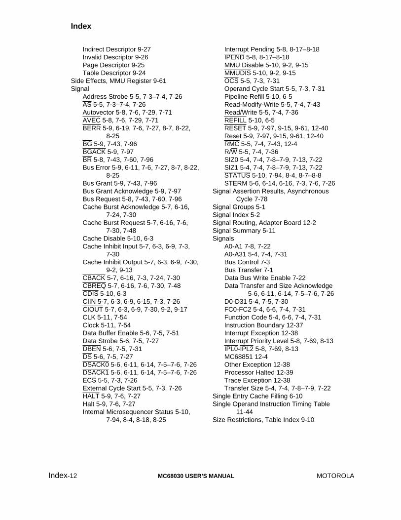
Index
Index
-12
MC68030 USER’S MANUAL
MOTOROLA
Indirect Descriptor 9-27Invalid Descriptor 9-26Page Descriptor 9-25Table Descriptor 9-24
Side Effects, MMU Register 9-61Signal
Address Strobe 5-5, 7-3–7-4, 7-26AS 5-5, 7-3–7-4, 7-26Autovector 5-8, 7-6, 7-29, 7-71AVEC 5-8, 7-6, 7-29, 7-71BERR 5-9, 6-19, 7-6, 7-27, 8-7, 8-22,
8-25BG 5-9, 7-43, 7-96BGACK 5-9, 7-97BR 5-8, 7-43, 7-60, 7-96Bus Error 5-9, 6-11, 7-6, 7-27, 8-7, 8-22,
8-25Bus Grant 5-9, 7-43, 7-96Bus Grant Acknowledge 5-9, 7-97Bus Request 5-8, 7-43, 7-60, 7-96Cache Burst Acknowledge 5-7, 6-16,
7-24, 7-30Cache Burst Request 5-7, 6-16, 7-6,
7-30, 7-48Cache Disable 5-10, 6-3Cache Inhibit Input 5-7, 6-3, 6-9, 7-3,
7-30Cache Inhibit Output 5-7, 6-3, 6-9, 7-30,
9-2, 9-13CBACK 5-7, 6-16, 7-3, 7-24, 7-30CBREQ 5-7, 6-16, 7-6, 7-30, 7-48CDIS 5-10, 6-3CIIN 5-7, 6-3, 6-9, 6-15, 7-3, 7-26CIOUT 5-7, 6-3, 6-9, 7-30, 9-2, 9-17CLK 5-11, 7-54Clock 5-11, 7-54Data Buffer Enable 5-6, 7-5, 7-51Data Strobe 5-6, 7-5, 7-27DBEN 5-6, 7-5, 7-31DS 5-6, 7-5, 7-27DSACK0 5-6, 6-11, 6-14, 7-5–7-6, 7-26DSACK1 5-6, 6-11, 6-14, 7-5–7-6, 7-26ECS 5-5, 7-3, 7-26External Cycle Start 5-5, 7-3, 7-26HALT 5-9, 7-6, 7-27Halt 5-9, 7-6, 7-27Internal Microsequencer Status 5-10,
7-94, 8-4, 8-18, 8-25
Interrupt Pending 5-8, 8-17–8-18IPEND 5-8, 8-17–8-18MMU Disable 5-10, 9-2, 9-15MMUDIS 5-10, 9-2, 9-15OCS 5-5, 7-3, 7-31Operand Cycle Start 5-5, 7-3, 7-31Pipeline Refill 5-10, 6-5Read-Modify-Write 5-5, 7-4, 7-43Read/Write 5-5, 7-4, 7-36REFILL 5-10, 6-5RESET 5-9, 7-97, 9-15, 9-61, 12-40Reset 5-9, 7-97, 9-15, 9-61, 12-40RMC 5-5, 7-4, 7-43, 12-4R/W 5-5, 7-4, 7-36SIZ0 5-4, 7-4, 7-8–7-9, 7-13, 7-22SIZ1 5-4, 7-4, 7-8–7-9, 7-13, 7-22STATUS 5-10, 7-94, 8-4, 8-7–8-8STERM 5-6, 6-14, 6-16, 7-3, 7-6, 7-26
Signal Assertion Results, Asynchronous Cycle 7-78
Signal Groups 5-1Signal Index 5-2Signal Routing, Adapter Board 12-2Signal Summary 5-11Signals
A0-A1 7-8, 7-22A0-A31 5-4, 7-4, 7-31Bus Control 7-3Bus Transfer 7-1Data Bus Write Enable 7-22Data Transfer and Size Acknowledge
5-6, 6-11, 6-14, 7-5–7-6, 7-26D0-D31 5-4, 7-5, 7-30FC0-FC2 5-4, 6-6, 7-4, 7-31Function Code 5-4, 6-6, 7-4, 7-31Instruction Boundary 12-37Interrupt Exception 12-38Interrupt Priority Level 5-8, 7-69, 8-13IPL0-IPL2 5-8, 7-69, 8-13MC68851 12-4Other Exception 12-38Processor Halted 12-39Trace Exception 12-38Transfer Size 5-4, 7-4, 7-8–7-9, 7-22
Single Entry Cache Filling 6-10Single Operand Instruction Timing Table
11-44Size Restrictions, Table Index 9-10
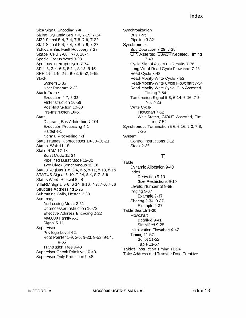
Index
MOTOROLA
MC68030 USER’S MANUAL
Index-13
Size Signal Encoding 7-8Sizing, Dynamic Bus 7-6, 7-19, 7-24SIZ0 Signal 5-4, 7-4, 7-8–7-9, 7-22SIZ1 Signal 5-4, 7-4, 7-8–7-9, 7-22Software Bus Fault Recovery 8-27Space, CPU 7-68, 7-70, 10-7Special Status Word 8-28Spurious Interrupt Cycle 7-74SR 1-8, 2-4, 6-5, 8-11, 8-13, 8-15SRP 1-5, 1-9, 2-5, 9-23, 9-52, 9-65Stack
System 2-36User Program 2-38
Stack FrameException 4-7, 8-32Mid-Instruction 10-59Post-Instruction 10-60Pre-Instruction 10-57
StateDiagram, Bus Arbitration 7-101Exception Processing 4-1Halted 4-1Normal Processing 4-1
State Frames, Coprocessor 10-20–10-21States, Wait 11-18Static RAM 12-18
Burst Mode 12-24Pipelined Burst Mode 12-30Two Clock Synchronous 12-18
Status Register 1-8, 2-4, 6-5, 8-11, 8-13, 8-15STATUS Signal 5-10, 7-94, 8-4, 8-7–8-8Status Word, Special 8-28STERM Signal 5-6, 6-14, 6-16, 7-3, 7-6, 7-26Structure Addressing 2-25Subroutine Calls, Nested 3-30Summary
Addressing Mode 2-31Coprocessor Instruction 10-72Effective Address Encoding 2-22M68000 Family A-1Signal 5-11
SupervisorPrivilege Level 4-2Root Pointer 1-9, 2-5, 9-23, 9-52, 9-54,
9-65Translation Tree 9-48
Supervisor Check Primitive 10-40Supervisor Only Protection 9-48
SynchronizationBus 7-95Pipeline 3-32
SynchronousBus Operation 7-28–7-29CIIN Asserted, CBACK Negated, Timing
7-48Cycle Signal Assertion Results 7-78Long Word Read Cycle Flowchart 7-48Read Cycle 7-48Read-Modify-Write Cycle 7-52Read-Modify-Write Cycle Flowchart 7-54Read-Modify-Write Cycle, CIIN Asserted,
Timing 7-54Termination Signal 5-6, 6-14, 6-16, 7-3,
7-6, 7-26Write Cycle
Flowchart 7-52Wait States, CIOUT Asserted, Tim-
ing 7-52Synchronous Termination 5-6, 6-16, 7-3, 7-6,
7-26System
Control Instructions 3-12Stack 2-36
T
TableDynamic Allocation 9-40Index
Derivation 9-10Size Restrictions 9-10
Levels, Number of 9-68Paging 9-37
Example 9-37Sharing 9-34, 9-37
Example 9-37Table Search 9-30
FlowchartDetailed 9-41Simplified 9-28
Initialization Flowchart 9-42Timing 11-52
Script 11-52Table 11-57
Tables, Instruction Timing 11-24Take Address and Transfer Data Primitive
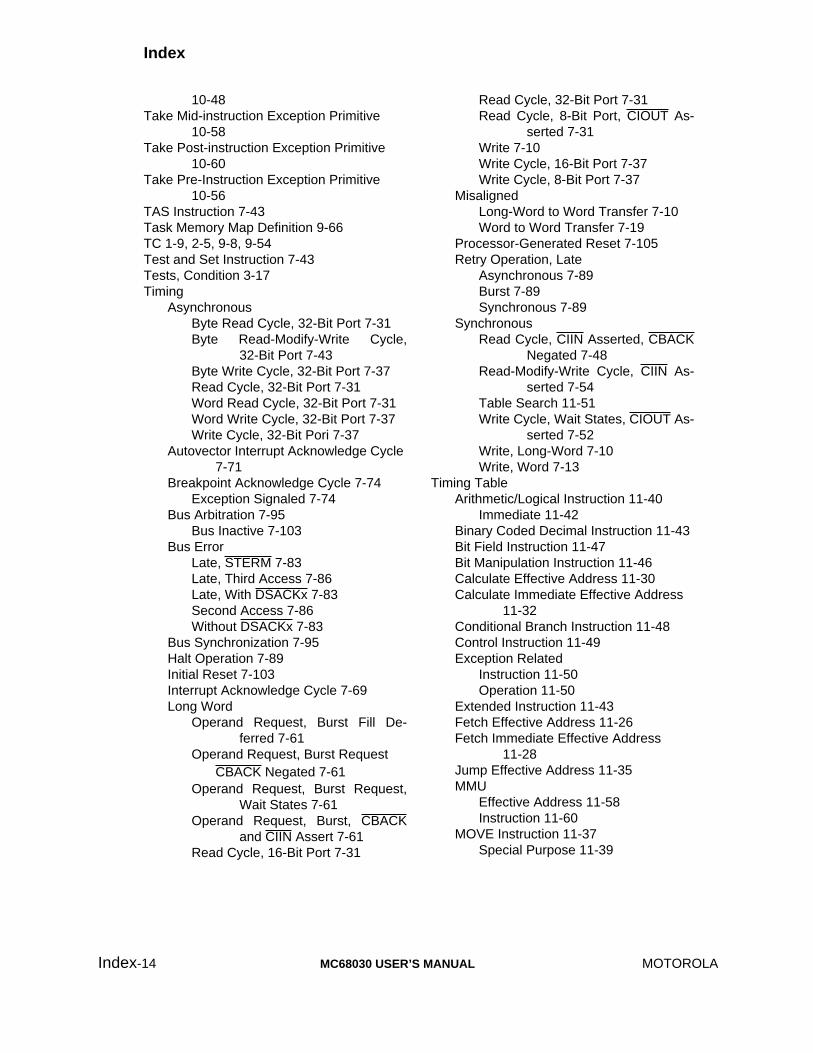
Index
Index
-14
MC68030 USER’S MANUAL
MOTOROLA
10-48Take Mid-instruction Exception Primitive
10-58Take Post-instruction Exception Primitive
10-60Take Pre-Instruction Exception Primitive
10-56TAS Instruction 7-43Task Memory Map Definition 9-66TC 1-9, 2-5, 9-8, 9-54Test and Set Instruction 7-43Tests, Condition 3-17Timing
AsynchronousByte Read Cycle, 32-Bit Port 7-31Byte Read-Modify-Write Cycle,
32-Bit Port 7-43Byte Write Cycle, 32-Bit Port 7-37Read Cycle, 32-Bit Port 7-31Word Read Cycle, 32-Bit Port 7-31Word Write Cycle, 32-Bit Port 7-37Write Cycle, 32-Bit Pori 7-37
Autovector Interrupt Acknowledge Cycle 7-71
Breakpoint Acknowledge Cycle 7-74Exception Signaled 7-74
Bus Arbitration 7-95Bus Inactive 7-103
Bus ErrorLate, STERM 7-83Late, Third Access 7-86Late, With DSACKx 7-83Second Access 7-86Without DSACKx 7-83
Bus Synchronization 7-95Halt Operation 7-89Initial Reset 7-103Interrupt Acknowledge Cycle 7-69Long Word
Operand Request, Burst Fill De-ferred 7-61
Operand Request, Burst RequestCBACK Negated 7-61
Operand Request, Burst Request,Wait States 7-61
Operand Request, Burst, CBACKand CIIN Assert 7-61
Read Cycle, 16-Bit Port 7-31
Read Cycle, 32-Bit Port 7-31Read Cycle, 8-Bit Port, CIOUT As-
serted 7-31Write 7-10Write Cycle, 16-Bit Port 7-37Write Cycle, 8-Bit Port 7-37
MisalignedLong-Word to Word Transfer 7-10Word to Word Transfer 7-19
Processor-Generated Reset 7-105Retry Operation, Late
Asynchronous 7-89Burst 7-89Synchronous 7-89
SynchronousRead Cycle, CIIN Asserted, CBACK
Negated 7-48Read-Modify-Write Cycle, CIIN As-
serted 7-54Table Search 11-51Write Cycle, Wait States, CIOUT As-
serted 7-52Write, Long-Word 7-10Write, Word 7-13
Timing TableArithmetic/Logical Instruction 11-40
Immediate 11-42Binary Coded Decimal Instruction 11-43Bit Field Instruction 11-47Bit Manipulation Instruction 11-46Calculate Effective Address 11-30Calculate Immediate Effective Address
11-32Conditional Branch Instruction 11-48Control Instruction 11-49Exception Related
Instruction 11-50Operation 11-50
Extended Instruction 11-43Fetch Effective Address 11-26Fetch Immediate Effective Address
11-28Jump Effective Address 11-35MMU
Effective Address 11-58Instruction 11-60
MOVE Instruction 11-37Special Purpose 11-39
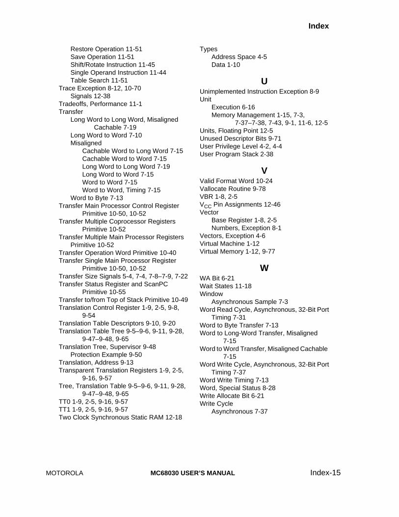
Index
MOTOROLA
MC68030 USER’S MANUAL
Index-15
Restore Operation 11-51Save Operation 11-51Shift/Rotate Instruction 11-45Single Operand Instruction 11-44Table Search 11-51
Trace Exception 8-12, 10-70Signals 12-38
Tradeoffs, Performance 11-1Transfer
Long Word to Long Word, Misaligned Cachable 7-19
Long Word to Word 7-10Misaligned
Cachable Word to Long Word 7-15Cachable Word to Word 7-15Long Word to Long Word 7-19Long Word to Word 7-15Word to Word 7-15Word to Word, Timing 7-15
Word to Byte 7-13Transfer Main Processor Control Register
Primitive 10-50, 10-52Transfer Multiple Coprocessor Registers
Primitive 10-52Transfer Multiple Main Processor Registers
Primitive 10-52Transfer Operation Word Primitive 10-40Transfer Single Main Processor Register
Primitive 10-50, 10-52Transfer Size Signals 5-4, 7-4, 7-8–7-9, 7-22Transfer Status Register and ScanPC
Primitive 10-55Transfer to/from Top of Stack Primitive 10-49Translation Control Register 1-9, 2-5, 9-8,
9-54Translation Table Descriptors 9-10, 9-20Translation Table Tree 9-5–9-6, 9-11, 9-28,
9-47–9-48, 9-65Translation Tree, Supervisor 9-48
Protection Example 9-50Translation, Address 9-13Transparent Translation Registers 1-9, 2-5,
9-16, 9-57Tree, Translation Table 9-5–9-6, 9-11, 9-28,
9-47–9-48, 9-65TT0 1-9, 2-5, 9-16, 9-57TT1 1-9, 2-5, 9-16, 9-57Two Clock Synchronous Static RAM 12-18
TypesAddress Space 4-5Data 1-10
U
Unimplemented Instruction Exception 8-9Unit
Execution 6-16Memory Management 1-15, 7-3,
7-37–7-38, 7-43, 9-1, 11-6, 12-5Units, Floating Point 12-5Unused Descriptor Bits 9-71User Privilege Level 4-2, 4-4User Program Stack 2-38
V
Valid Format Word 10-24Vallocate Routine 9-78VBR 1-8, 2-5V
CC
Pin Assignments 12-46Vector
Base Register 1-8, 2-5Numbers, Exception 8-1
Vectors, Exception 4-6Virtual Machine 1-12Virtual Memory 1-12, 9-77
W
WA Bit 6-21Wait States 11-18Window
Asynchronous Sample 7-3Word Read Cycle, Asynchronous, 32-Bit Port
Timing 7-31Word to Byte Transfer 7-13Word to Long-Word Transfer, Misaligned
7-15Word to Word Transfer, Misaligned Cachable
7-15Word Write Cycle, Asynchronous, 32-Bit Port
Timing 7-37Word Write Timing 7-13Word, Special Status 8-28Write Allocate Bit 6-21Write Cycle
Asynchronous 7-37
Index
Index
-16
MC68030 USER’S MANUAL
MOTOROLA
Flowchart 7-3732-Bit Port, Timing 7-37
Synchronous 7-51Flowchart 7-52
Wait States, CIOUT Asserted, Timing 7-52
Write Pending Buffer 11-5Write Protection 9-48Write Timing
Long Word 7-10Word 7-13
Write to Previously Evaluated Effective Address
Primitive 10-46