mp2493 2a, 36v, low emi step-down converter with
TRANSCRIPT
MP2493 2A, 36V, Low EMI Step-Down Converter with Programmable Output Current Limit
MP2493 Rev. 1.0 www.MonolithicPower.com 1 2/12/2014 MPS Proprietary Information. Patent Protected. Unauthorized Photocopy and Duplication Prohibited. © 2014 MPS. All Rights Reserved.
The Future of Analog IC Technology
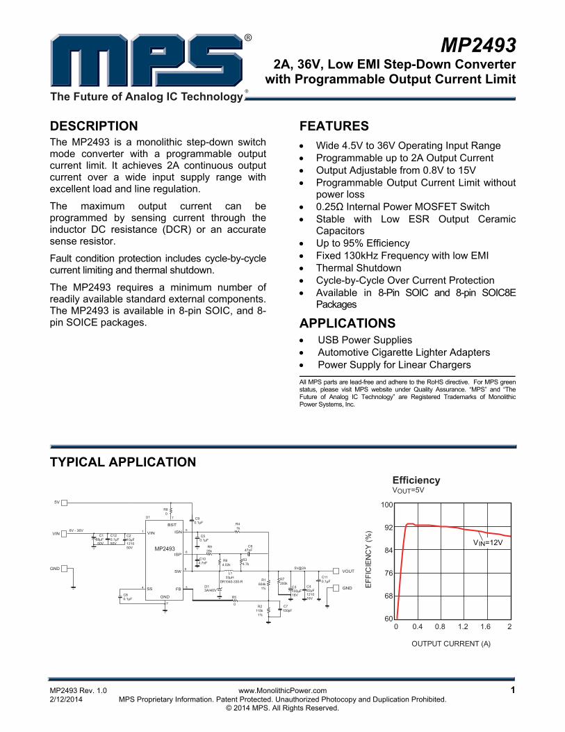
DESCRIPTION The MP2493 is a monolithic step-down switch mode converter with a programmable output current limit. It achieves 2A continuous output current over a wide input supply range with excellent load and line regulation.
The maximum output current can be programmed by sensing current through the inductor DC resistance (DCR) or an accurate sense resistor.
Fault condition protection includes cycle-by-cycle current limiting and thermal shutdown.
The MP2493 requires a minimum number of readily available standard external components. The MP2493 is available in 8-pin SOIC, and 8-pin SOICE packages.
FEATURES • Wide 4.5V to 36V Operating Input Range • Programmable up to 2A Output Current • Output Adjustable from 0.8V to 15V • Programmable Output Current Limit without
power loss • 0.25Ω Internal Power MOSFET Switch • Stable with Low ESR Output Ceramic
Capacitors • Up to 95% Efficiency • Fixed 130kHz Frequency with low EMI • Thermal Shutdown • Cycle-by-Cycle Over Current Protection • Available in 8-Pin SOIC and 8-pin SOIC8E
Packages
APPLICATIONS • USB Power Supplies • Automotive Cigarette Lighter Adapters • Power Supply for Linear Chargers All MPS parts are lead-free and adhere to the RoHS directive. For MPS green status, please visit MPS website under Quality Assurance. “MPS” and “The Future of Analog IC Technology” are Registered Trademarks of Monolithic Power Systems, Inc.
TYPICAL APPLICATION
C647nF
R64.02k
R920k
R34.7k
R8 0
U1
R7200k
C7150pF
R5
0
R4 1k
D1 3A/40V
VIN
BST
ISN
ISP
SS
SW
GND
FB
1
4
2
3
8
6
5
7
5V
6V - 36VVIN
GND VOUT
GND
MP2493 C104.7nF
+
+
EfficiencyVOUT=5V
OUTPUT CURRENT (A)
EFF
ICIE
NC
Y (%
)
60
68
76
84
92
100
0 0.4 0.8 1.2 1.6 2
VIN=12V
MP2493 – 2A, 36V, LOW EMI STEP-DOWN WITH PROGRAMMABLE OUTPUT CURRENT LIMIT
MP2493 Rev. 1.0 www.MonolithicPower.com 2 2/12/2014 MPS Proprietary Information. Patent Protected. Unauthorized Photocopy and Duplication Prohibited. © 2014 MPS. All Rights Reserved.
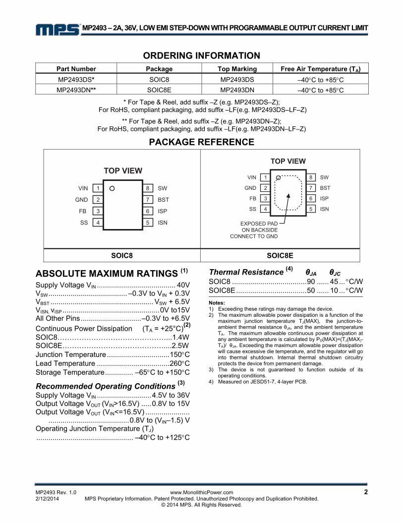
ORDERING INFORMATION Part Number Package Top Marking Free Air Temperature (TA) MP2493DS* SOIC8 MP2493DS –40°C to +85°C MP2493DN** SOIC8E MP2493DN –40°C to +85°C
* For Tape & Reel, add suffix –Z (e.g. MP2493DS–Z); For RoHS, compliant packaging, add suffix –LF(e.g. MP2493DS–LF–Z)
** For Tape & Reel, add suffix –Z (e.g. MP2493DN–Z); For RoHS, compliant packaging, add suffix –LF(e.g. MP2493DN–LF–Z)
PACKAGE REFERENCE
VIN
GND
FB
SS
SW
BST
ISP
ISN
1
2
3
4
8
7
6
5
TOP VIEW
VIN
GND
FB
SS
SW
BST
ISP
ISN
1
2
3
4
8
7
6
5
TOP VIEW
EXPOSED PADON BACKSIDE
CONNECT TO GND
SOIC8 SOIC8E
ABSOLUTE MAXIMUM RATINGS (1) Supply Voltage VIN ....................................... 40V VSW....................................... –0.3V to VIN + 0.3V VBST ................................................... VSW + 6.5V VISN, vISP ................................................0V to15V All Other Pins..............................–0.3V to +6.5V Continuous Power Dissipation (TA = +25°C)(2) SOIC8………………………………………...1.4W SOIC8E……………………………………....2.5W Junction Temperature...............................150°C Lead Temperature ....................................260°C Storage Temperature.............. –65°C to +150°C
Recommended Operating Conditions (3) Supply Voltage VIN ...........................4.5V to 36V Output Voltage VOUT (VIN>16.5V) .....0.8V to 15V Output Voltage VOUT (VIN<=16.5V) ...................... ........................................0.8V to (VIN–1.5) V Operating Junction Temperature (TJ) ................................................ –40°C to +125°C
Thermal Resistance (4) θJA θJC SOIC8 .....................................90 ...... 45 ... °C/W SOIC8E...................................50 ...... 10 ... °C/W Notes: 1) Exceeding these ratings may damage the device. 2) The maximum allowable power dissipation is a function of the
maximum junction temperature TJ(MAX), the junction-to-ambient thermal resistance θJA, and the ambient temperature TA. The maximum allowable continuous power dissipation at any ambient temperature is calculated by PD(MAX)=(TJ(MAX)-TA)/ θJA. Exceeding the maximum allowable power dissipation will cause excessive die temperature, and the regulator will go into thermal shutdown. Internal thermal shutdown circuitry protects the device from permanent damage.
3) The device is not guaranteed to function outside of its operating conditions.
4) Measured on JESD51-7, 4-layer PCB.
MP2493 – 2A, 36V, LOW EMI STEP-DOWN WITH PROGRAMMABLE OUTPUT CURRENT LIMIT
MP2493 Rev. 1.0 www.MonolithicPower.com 3 2/12/2014 MPS Proprietary Information. Patent Protected. Unauthorized Photocopy and Duplication Prohibited. © 2014 MPS. All Rights Reserved.
ELECTRICAL CHARACTERISTICS VIN = 12V, TA = +25°C, unless otherwise noted. Parameters Symbol Condition Min Typ Max Units
Feedback Voltage VFB 4.5V ≤ VIN ≤ 36V 0.78 0.8 0.82 V
Feedback Bias Current IBIAS(FB) VFB = 0.8V 10 nA
Switch On Resistance RDS(ON) 0.25 Ω
Switch Leakage VEN = 0V, VSW = 0V 0.1 10 μA
Current Limit (5) Peak current limit 2.5 3.0 3.5 A
Oscillator Frequency fSW VFB = 0.6V 100 130 160 kHz
Switching frequency VFB = 0V 35 kHz
Boot-Strap Voltage VBST - VSW 4.5 V
Minimum On Time (5) tON VFB = 1V 100 ns
SW rising edge (5) trise VIN=12V, VO=5V, IO=1.5A 50 ns
SW falling edge (5) tfall VIN=12V, VO=5V, IO=1.5A 50 ns
Under Voltage Lockout Threshold Rising 3.0 3.3 3.6 V
Under Voltage Lockout Threshold Hysteresis 150 mV
EN Input Low Voltage (6) 0.4 V
En Input High Voltage (6) 1.8 V
EN Input Bias Current (6) VEN = 0-6V –10 –2 10 μA
Supply Current (Shutdown) VEN = 0V 4 10 μA
Supply Current (Quiescent) VEN = 2V, VFB = 1V 500 800 μA
Thermal Shutdown(5) 150 °C
Current Sense Voltage VISP –VISN VISP, VISN 0.4–15V 90 100 110 mV
Input Bias Current (ISN, ISP) IBIAS (ISN,ISP) VISP, VISN 0.4–15V –1 0.1 +1 uA Note: 5) Guaranteed by design 6) Enable function is only available for the MP2493DQ
MP2493 – 2A, 36V, LOW EMI STEP-DOWN WITH PROGRAMMABLE OUTPUT CURRENT LIMIT
MP2493 Rev. 1.0 www.MonolithicPower.com 4 2/12/2014 MPS Proprietary Information. Patent Protected. Unauthorized Photocopy and Duplication Prohibited. © 2014 MPS. All Rights Reserved.
PIN FUNCTIONS Pin# Name Description
1 VIN
Supply Voltage. The MP2493 operates from a +4.5V to +36V unregulated input. CIN is needed to prevent large voltage spikes from appearing at the input. Put CIN as close to the IC as possible. It is the drain of the internal power device and power supply for the whole chip.
2 GND Exposed Pad
Ground. This pin is the voltage reference for the regulated output voltage. For this reason care must be taken in its layout. This node should be placed outside of the D1 to CIN ground path to prevent switching current spikes from inducing voltage noise into the part. Exposed Pad must be connected with Ground pin in SOIC8E package.
3 FB
Feedback. An external resistor divider from the output to GND, tapped to the FB pin sets the output voltage. To prevent current limit run away during a short circuit fault condition the frequency-fold-back comparator lowers the oscillator frequency when the FB voltage is below 250mV.
4 SS Connect to an external capacitor used for Soft-Start and compensation for current limiting loop.
5 ISN Negative Current Sense Input for load current limiting. 6 ISP Positive Current Sense
7 BST
Bootstrap. This capacitor is needed to drive the power switch’s gate above the supply voltage. It is connected between SW and BST pins to form a floating supply across the power switch driver. An on-chip regulator is used to charge up the external boot-strap capacitor. If the on-chip regulator is not strong enough, one optional diode can be connected from IN or OUT to charge the external boot-strap capacitor.
8 SW Switch Output. It is the source of power device.
MP2493 – 2A, 36V, LOW EMI STEP-DOWN WITH PROGRAMMABLE OUTPUT CURRENT LIMIT
MP2493 Rev. 1.0 www.MonolithicPower.com 5 2/12/2014 MPS Proprietary Information. Patent Protected. Unauthorized Photocopy and Duplication Prohibited. © 2014 MPS. All Rights Reserved.
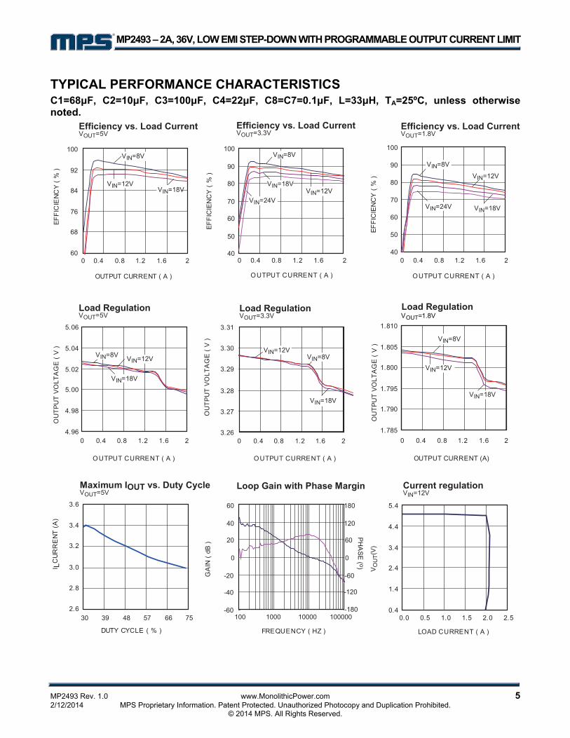
TYPICAL PERFORMANCE CHARACTERISTICS C1=68μF, C2=10μF, C3=100μF, C4=22μF, C8=C7=0.1μF, L=33μH, TA=25ºC, unless otherwise noted.
Load RegulationLoad RegulationVOUT=5V
Load RegulationVOUT=3.3V
OUTPUT CURRENT (A)
VOUT=1.8V
60
68
76
84
92
100
0 0.4 0.8 1.2 1.6 2
OUTPUT CURRENT ( A )
EFFI
CIE
NC
Y (
% )
VIN=18VVIN=12V
VIN=8V
Efficiency vs. Load CurrentVOUT=5V
Efficiency vs. Load CurrentVOUT=3.3V
Efficiency vs. Load CurrentVOUT=1.8V
40
50
60
70
80
90
100
0 0.4 0.8 1.2 1.6 2
OUTPUT CURRENT ( A ) OUTPUT CURRENT ( A )
EFFI
CIE
NC
Y (
% )
EFFI
CIE
NC
Y (
% )
VIN=8V
VIN=12VVIN=18V
VIN=24V
40
50
60
70
80
90
100
0 0.4 0.8 1.2 1.6 2
VIN=12V
VIN=8V
VIN=18VVIN=24V
4.96
4.98
5.00
5.02
5.04
5.06
0 0.4 0.8 1.2 1.6 2
OUTPUT CURRENT ( A ) OUTPUT CURRENT ( A )
OU
TPU
T V
OLT
AG
E (
V )
VIN=12VVIN=8V
VIN=18V
3.26
3.27
3.28
3.29
3.30
3.31
0 0.4 0.8 1.2 1.6 2
OU
TPU
T V
OLT
AG
E (
V )
OU
TPU
T V
OLT
AG
E (
V )VIN=12V
VIN=18V
VIN=8V
1.785
1.790
1.795
1.800
1.805
1.810
0 0.4 0.8 1.2 1.6 2
VIN=8V
VIN=18V
VIN=12V
2.6
2.8
3.0
3.2
3.4
3.6
30 39 48 57 66 75
DUTY CYCLE ( % )
I LC
UR
RE
NT
(A)
Maximum IOUT vs. Duty CycleVOUT=5V
-60
-40
-20
0
20
40
60
100 1000 10000 100000
FREQUENCY ( HZ )
GA
IN (
dB )
-180
-120
-60
0
60
120
180
PH
ASE
( o)
Loop Gain with Phase Margin
0.4
1.4
2.4
3.4
4.4
5.4
0.0 0.5 1.0 1.5 2.0 2.5
LOAD CURRENT ( A )
VO
UT(
V)
Current regulationVIN=12V
MP2493 – 2A, 36V, LOW EMI STEP-DOWN WITH PROGRAMMABLE OUTPUT CURRENT LIMIT
MP2493 Rev. 1.0 www.MonolithicPower.com 6 2/12/2014 MPS Proprietary Information. Patent Protected. Unauthorized Photocopy and Duplication Prohibited. © 2014 MPS. All Rights Reserved.
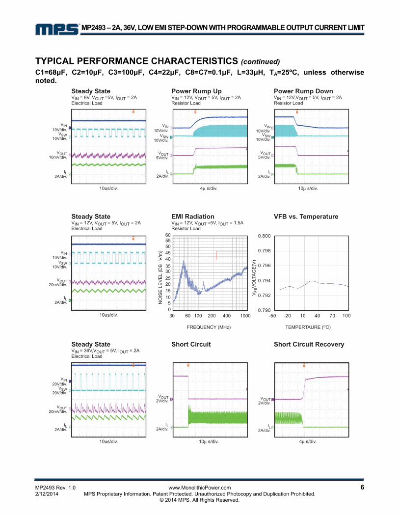
TYPICAL PERFORMANCE CHARACTERISTICS (continued) C1=68μF, C2=10μF, C3=100μF, C4=22μF, C8=C7=0.1μF, L=33μH, TA=25ºC, unless otherwise noted.
VIN10V/div.
VSW10V/div.
VOUT10mV/div.
VOUT5V/div.
VOUT5V/div.
IL2A/div.
10us/div.
VIN10V/div.
VSW10V/div.
IL2A/div.
IL2A/div.
4μ s/div.
VIN10V/div.
VSW10V/div.
10μ s/div.
VIN10V/div.
VSW10V/div.
VOUT20mV/div.
IL2A/div.
10us/div.
VFB vs. Temperature
VIN20V/div.
VSW20V/div.
VOUT20mV/div.
VOUT2V/div. VOUT
2V/div.
IL2A/div.
IL2A/div.
IL2A/div.
10us/div. 10μ s/div.
Short Circuit
4μ s/div.
Short Circuit Recovery
3005
1015202530354045505560
60 100 200 400 1000
FREQUENCY (MHz)
NO
ISE
LE
VE
L (D
B
V/m
)
0.790
0.792
0.794
0.796
0.798
0.800
-50 -20 10 40 70 100
TEMPERTAURE (OC)
VFB
VO
LTA
GE
(V)

MP2493 – 2A, 36V, LOW EMI STEP-DOWN WITH PROGRAMMABLE OUTPUT CURRENT LIMIT
MP2493 Rev. 1.0 www.MonolithicPower.com 7 2/12/2014 MPS Proprietary Information. Patent Protected. Unauthorized Photocopy and Duplication Prohibited. © 2014 MPS. All Rights Reserved.
OPERATION Main Control Loop The MP2493 is a current mode buck regulator. That is, the error amplifier (EA) output voltage is proportional to the peak inductor current.
At the beginning of a cycle, the integrated high side power switch M1 (Fig.1) is off; the EA output voltage is higher than the current sense amplifier output; and the current comparator’s output is low. The rising edge of the 130kHz clock signal sets the RS Flip-Flop. Its output turns on M1 thus connecting the SW pin and inductor to the input supply.
The increasing inductor current is sensed and amplified by the Current Sense Amplifier. Ramp compensation is added to Current Sense Amplifier output and compared to the Error Amplifier output by the PWM Comparator. When the Current Sense Amplifier plus Slope Compensation signal exceeds the EA output voltage, the RS Flip-Flop is reset and the MP2493 reverts to its initial M1 off state.
If the Current Sense Amplifier plus Slope Compensation signal does not exceed the COMP voltage, then the falling edge of the CLK resets the Flip-Flop.
The output of the Error Amplifier integrates the voltage difference between the feedback and the 0.8V bandgap reference. The polarity is such that a FB pin voltage lower than 0.8V increases the EA output voltage. Since the EA output voltage is proportional to the peak inductor current, an increase in its voltage increases current delivered to the output. An external Schottky Diode (D1) carries the inductor current when M1 is off.
Load Current Limiting Loop The output current information is sensed via the ISP and ISN pins. The regulation threshold is set at 100mV. If VSENSE, the difference of VISP and VISN, is less than 100mV, the output voltage of the power supply will be set by the FB pin. If VSENSE reaches 100mV, the current limit loop will pull down SS and regulate the output at a constant current determined by the external sense resistor. The external capacitor on SS pin is the dominant compensation capacitor for load current regulation loop. The capacitor has normal value of 100nF, which will put the bandwidth of load current regulation loop to be less than 1 kHz. When VSENSE is higher than 100mV, SS will not drop down to the final regulation level immediately. It will cause the load current to be higher than the programmed level for a short period. A fast comparator is added to shut down power switch when the average load current is higher than 120% of the programmed current limit level.
An inductor DC resistance (DCR) or accurate sense resistor can be used for load current sensing.

MP2493 – 2A, 36V, LOW EMI STEP-DOWN WITH PROGRAMMABLE OUTPUT CURRENT LIMIT
MP2493 Rev. 1.0 www.MonolithicPower.com 8 2/12/2014 MPS Proprietary Information. Patent Protected. Unauthorized Photocopy and Duplication Prohibited. © 2014 MPS. All Rights Reserved.
ISP
ISN
4.0V
SS
VIN
SS
FB
SW
X13.5
BSTREGULATOR
100mV
DRIVER
PWM COMPARATOR
CURRENT LIMIT
COMPARATOR
RSEN 25m
M1
1pF
3398k
33pF
ER
GND
ENABLE
REGULATOR
ENOSCILLATOR
150kHz
REFERENCE
CURRENT SENSE AMPLIFIER
RAMP GENERATOR
POR REGULATOR
S
R
R
Q
D
++
--
+--
--
+
+
--
+--
Figure 1—Functional Block Diagram
MP2493 – 2A, 36V, LOW EMI STEP-DOWN WITH PROGRAMMABLE OUTPUT CURRENT LIMIT
MP2493 Rev. 1.0 www.MonolithicPower.com 9 2/12/2014 MPS Proprietary Information. Patent Protected. Unauthorized Photocopy and Duplication Prohibited. © 2014 MPS. All Rights Reserved.
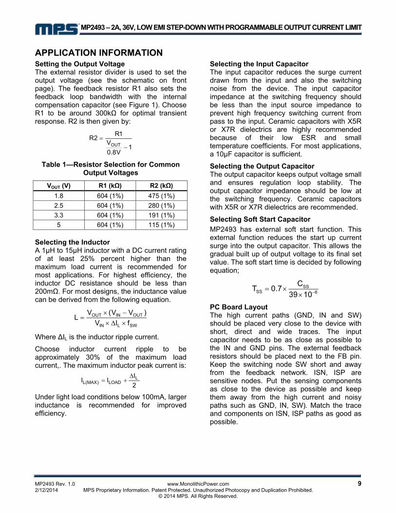
APPLICATION INFORMATION Setting the Output Voltage The external resistor divider is used to set the output voltage (see the schematic on front page). The feedback resistor R1 also sets the feedback loop bandwidth with the internal compensation capacitor (see Figure 1). Choose R1 to be around 300kΩ for optimal transient response. R2 is then given by:
1V8.0
V1R2R
OUT −=
Table 1—Resistor Selection for Common Output Voltages
VOUT (V) R1 (kΩ) R2 (kΩ) 1.8 604 (1%) 475 (1%) 2.5 604 (1%) 280 (1%) 3.3 604 (1%) 191 (1%) 5 604 (1%) 115 (1%)
Selecting the Inductor A 1µH to 15µH inductor with a DC current rating of at least 25% percent higher than the maximum load current is recommended for most applications. For highest efficiency, the inductor DC resistance should be less than 200mΩ. For most designs, the inductance value can be derived from the following equation.
SWLIN
OUTINOUT
fIV)VV(V
L×Δ×−×
=
Where ΔIL is the inductor ripple current.
Choose inductor current ripple to be approximately 30% of the maximum load current,. The maximum inductor peak current is:
2I
II LLOAD)MAX(L
Δ+=
Under light load conditions below 100mA, larger inductance is recommended for improved efficiency.
Selecting the Input Capacitor The input capacitor reduces the surge current drawn from the input and also the switching noise from the device. The input capacitor impedance at the switching frequency should be less than the input source impedance to prevent high frequency switching current from pass to the input. Ceramic capacitors with X5R or X7R dielectrics are highly recommended because of their low ESR and small temperature coefficients. For most applications, a 10µF capacitor is sufficient.
Selecting the Output Capacitor The output capacitor keeps output voltage small and ensures regulation loop stability. The output capacitor impedance should be low at the switching frequency. Ceramic capacitors with X5R or X7R dielectrics are recommended.
Selecting Soft Start Capacitor MP2493 has external soft start function. This external function reduces the start up current surge into the output capacitor. This allows the gradual built up of output voltage to its final set value. The soft start time is decided by following equation;
SSSS 6
CT 0.739 10−= ×
×
PC Board Layout The high current paths (GND, IN and SW) should be placed very close to the device with short, direct and wide traces. The input capacitor needs to be as close as possible to the IN and GND pins. The external feedback resistors should be placed next to the FB pin. Keep the switching node SW short and away from the feedback network. ISN, ISP are sensitive nodes. Put the sensing components as close to the device as possible and keep them away from the high current and noisy paths such as GND, IN, SW). Match the trace and components on ISN, ISP paths as good as possible.
MP2493 – 2A, 36V, LOW EMI STEP-DOWN WITH PROGRAMMABLE OUTPUT CURRENT LIMIT
MP2493 Rev. 1.0 www.MonolithicPower.com 10 2/12/2014 MPS Proprietary Information. Patent Protected. Unauthorized Photocopy and Duplication Prohibited. © 2014 MPS. All Rights Reserved.
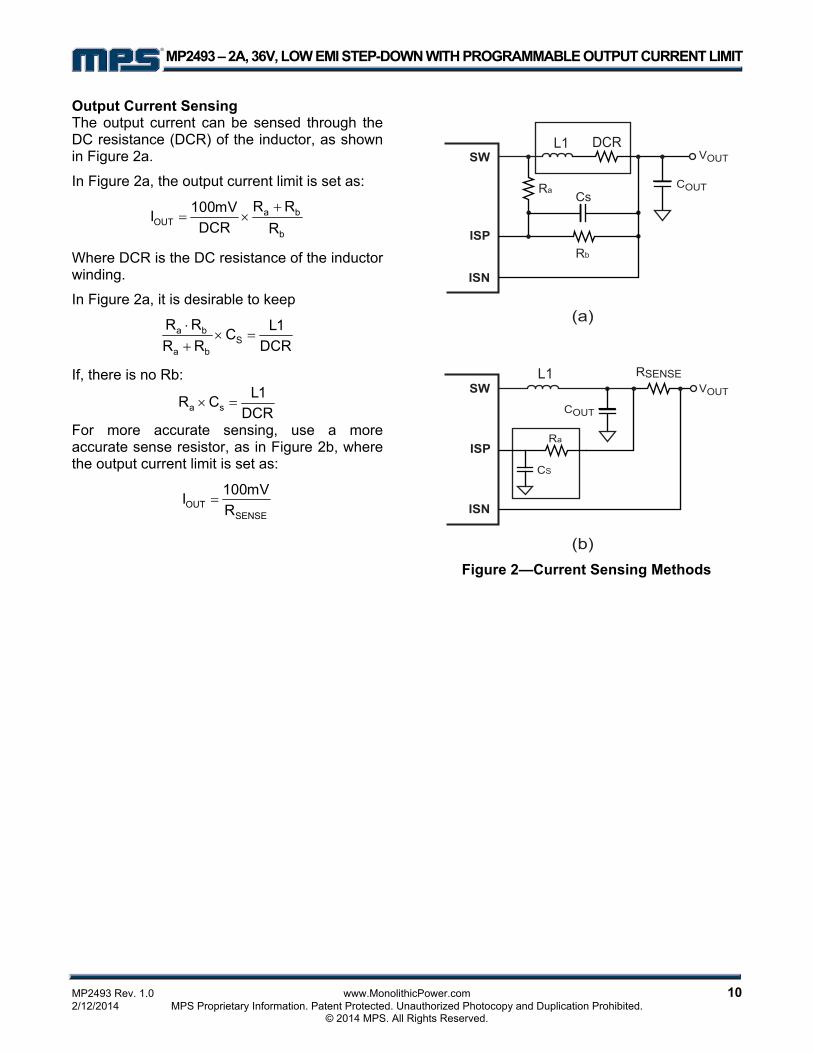
Output Current Sensing The output current can be sensed through the DC resistance (DCR) of the inductor, as shown in Figure 2a.
In Figure 2a, the output current limit is set as:
a bOUT
b
R R100mVIDCR R
+= ×
Where DCR is the DC resistance of the inductor winding.
In Figure 2a, it is desirable to keep
a bS
a b
R R L1CR R DCR
⋅× =
+
If, there is no Rb:
× =a sL1R C
DCR
For more accurate sensing, use a more accurate sense resistor, as in Figure 2b, where the output current limit is set as:
OUTSENSE
100mVIR
=
Figure 2—Current Sensing Methods

MP2493 – 2A, 36V, LOW EMI STEP-DOWN WITH PROGRAMMABLE OUTPUT CURRENT LIMIT
MP2493 Rev. 1.0 www.MonolithicPower.com 11 2/12/2014 MPS Proprietary Information. Patent Protected. Unauthorized Photocopy and Duplication Prohibited. © 2014 MPS. All Rights Reserved.
PACKAGE INFORMATION
SOIC8
0.016(0.41)0.050(1.27)0o-8o
DETAIL "A"
0.010(0.25)0.020(0.50) x 45o
SEE DETAIL "A"
0.0075(0.19)0.0098(0.25)
0.150(3.80)0.157(4.00)PIN 1 ID
0.050(1.27)BSC
0.013(0.33)0.020(0.51)
SEATING PLANE0.004(0.10)0.010(0.25)
0.189(4.80)0.197(5.00)
0.053(1.35)0.069(1.75)
TOP VIEW
FRONT VIEW
0.228(5.80)0.244(6.20)
SIDE VIEW
1 4
8 5
RECOMMENDED LAND PATTERN
0.213(5.40)
0.063(1.60)
0.050(1.27)0.024(0.61)
NOTE:
1) CONTROL DIMENSION IS IN INCHES. DIMENSION IN BRACKET IS IN MILLIMETERS. 2) PACKAGE LENGTH DOES NOT INCLUDE MOLD FLASH, PROTRUSIONS OR GATE BURRS. 3) PACKAGE WIDTH DOES NOT INCLUDE INTERLEAD FLASH OR PROTRUSIONS. 4) LEAD COPLANARITY (BOTTOM OF LEADS AFTER FORMING) SHALL BE 0.004" INCHES MAX. 5) DRAWING CONFORMS TO JEDEC MS-012, VARIATION AA. 6) DRAWING IS NOT TO SCALE.
0.010(0.25) BSCGAUGE PLANE

MP2493 – 2A, 36V, 130kHz STEP-DOWN WITH PROGRAMMABLE OUTPUT CURRENT LIMIT
NOTICE: The information in this document is subject to change without notice. Please contact MPS for current specifications. Users should warrant and guarantee that third party Intellectual Property rights are not infringed upon when integrating MPS products into any application. MPS will not assume any legal responsibility for any said applications.
MP2493 Rev. 1.0 www.MonolithicPower.com 12 2/12/2014 MPS Proprietary Information. Patent Protected. Unauthorized Photocopy and Duplication Prohibited. © 2014 MPS. All Rights Reserved.
SOIC8E
Mouser Electronics
Authorized Distributor
Click to View Pricing, Inventory, Delivery & Lifecycle Information: Monolithic Power Systems (MPS):
MP2493DN-LF MP2493DN-LF-Z MP2493DS-LF MP2493DS-LF-Z MP24943DN-LF-P MP24943DS-LF-P
MP2493DN-LF-P MP2493DS-LF-P