mp6532 5v to 60v, three-phase brushless dc motor pre … to 60v, three-phase brushless dc motor...
TRANSCRIPT
MP6532 5V to 60V, Three-Phase Brushless
DC Motor Pre-Driver
MP6532 Rev. 1.11 www.MonolithicPower.com 1 9/6/2015 MPS Proprietary Information. Patent Protected. Unauthorized Photocopy and Duplication Prohibited. © 2015 MPS. All Rights Reserved.
The Future of Analog IC Technology
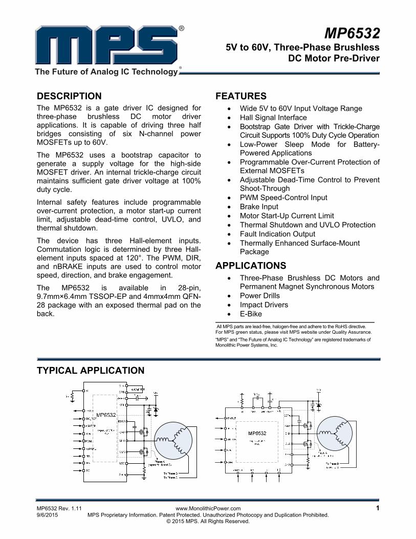
DESCRIPTION The MP6532 is a gate driver IC designed for three-phase brushless DC motor driver applications. It is capable of driving three half bridges consisting of six N-channel power MOSFETs up to 60V.
The MP6532 uses a bootstrap capacitor to generate a supply voltage for the high-side MOSFET driver. An internal trickle-charge circuit maintains sufficient gate driver voltage at 100% duty cycle.
Internal safety features include programmable over-current protection, a motor start-up current limit, adjustable dead-time control, UVLO, and thermal shutdown.
The device has three Hall-element inputs. Commutation logic is determined by three Hall-element inputs spaced at 120°. The PWM, DIR, and nBRAKE inputs are used to control motor speed, direction, and brake engagement.
The MP6532 is available in 28-pin, 9.7mm×6.4mm TSSOP-EP and 4mmx4mm QFN-28 package with an exposed thermal pad on the back.
FEATURES Wide 5V to 60V Input Voltage Range Hall Signal Interface Bootstrap Gate Driver with Trickle-Charge
Circuit Supports 100% Duty Cycle Operation Low-Power Sleep Mode for Battery-
Powered Applications Programmable Over-Current Protection of
External MOSFETs Adjustable Dead-Time Control to Prevent
Shoot-Through PWM Speed-Control Input Brake Input Motor Start-Up Current Limit Thermal Shutdown and UVLO Protection Fault Indication Output Thermally Enhanced Surface-Mount
Package
APPLICATIONS Three-Phase Brushless DC Motors and
Permanent Magnet Synchronous Motors Power Drills Impact Drivers E-Bike
All MPS parts are lead-free, halogen-free and adhere to the RoHS directive. For MPS green status, please visit MPS website under Quality Assurance.
“MPS” and “The Future of Analog IC Technology” are registered trademarks of Monolithic Power Systems, Inc.
TYPICAL APPLICATION
MP6532 – 5V TO 60V, THREE PHASE BLDC MOTOR PRE-DRIVER
MP6532 Rev. 1.11 www.MonolithicPower.com 2 9/6/2015 MPS Proprietary Information. Patent Protected. Unauthorized Photocopy and Duplication Prohibited. © 2015 MPS. All Rights Reserved.
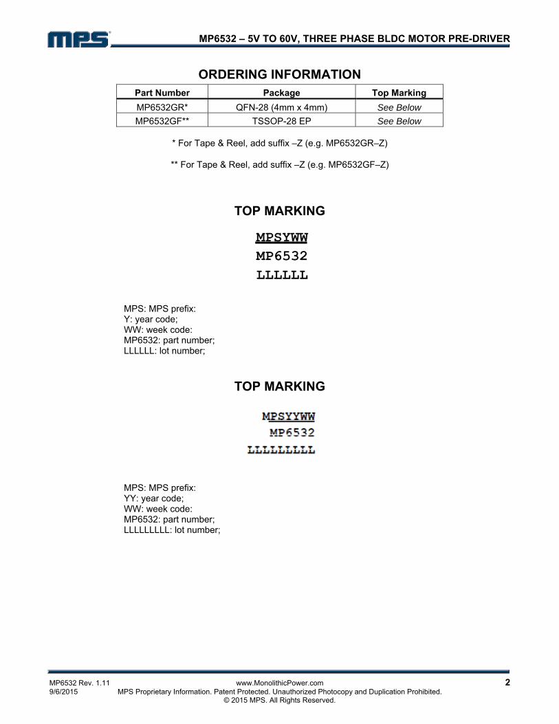
ORDERING INFORMATION Part Number Package Top Marking
MP6532GR* QFN-28 (4mm x 4mm) See Below
MP6532GF** TSSOP-28 EP See Below
* For Tape & Reel, add suffix –Z (e.g. MP6532GR–Z)
** For Tape & Reel, add suffix –Z (e.g. MP6532GF–Z)
TOP MARKING
MPS: MPS prefix: Y: year code; WW: week code: MP6532: part number; LLLLLL: lot number;
TOP MARKING
MPS: MPS prefix: YY: year code; WW: week code: MP6532: part number; LLLLLLLLL: lot number;

MP6532 – 5V TO 60V, THREE PHASE BLDC MOTOR PRE-DRIVER
MP6532 Rev. 1.11 www.MonolithicPower.com 3 9/6/2015 MPS Proprietary Information. Patent Protected. Unauthorized Photocopy and Duplication Prohibited. © 2015 MPS. All Rights Reserved.
PACKAGE REFERENCE
TOP VIEW TOP VIEW
QFN-28 (4mm×4mm) TSSOP-28 EP
ABSOLUTE MAXIMUM RATINGS (1) Input Voltage VIN .............................-0.3V to 65V CPA ................................................-0.3V to 60V CPB .............................................-0.3V to 12.5V VREG..............................................-0.3V to 13V BSTA/B/C .......................................-0.3V to 70V GHA/B/C .........................................-0.3V to 70V SHA/B/C .........................................-0.3V to 65V GLA/B/C..........................................-0.3V to 13V LSS ...................................................-0.3V to 1V All Other Pins to AGND..................-0.3V to 6.5V
Continuous Power Dissipation (TA = +25°C) (2)
QFN-28 (4mm x 4mm)…………………… 2.9W TSSOP-28 EP............................................ 3.9W Storage Temperature............... -55C to +150C Junction Temperature.............................+150C Lead Temperature (Solder).....................+260C
Recommended Operating Conditions (3) Input Voltage VIN .................................5V to 60V OC_REF Voltage VOC .................0.125V to 2.4V Operating Junct. Temp (TJ)...... -40C to +125C
Thermal Resistance (4) θJA θJC QFN-28 (4mm×4mm)..............42 ....... 9 .... °C/W TSSOP-28 EP.........................32 ....... 6 .... °C/W
Notes: 1) Exceeding these ratings may damage the device. 2) The maximum allowable power dissipation is a function of the
maximum junction temperature TJ (MAX), the junction-to-ambient thermal resistance θJA, and the ambient temperature TA. The maximum allowable continuous power dissipation at any ambient temperature is calculated by PD (MAX) = (TJ
(MAX)-TA)/θJA. Exceeding the maximum allowable power dissipation will cause excessive die temperature, and the regulator will go into thermal shutdown. Internal thermal shutdown circuitry protects the device from permanent damage.
3) The device is not guaranteed to function outside of its operating conditions.
4) Measured on JESD51-7, 4-layer PCB.
MP6532 – 5V TO 60V, THREE PHASE BLDC MOTOR PRE-DRIVER
MP6532 Rev. 1.11 www.MonolithicPower.com 4 9/6/2015 MPS Proprietary Information. Patent Protected. Unauthorized Photocopy and Duplication Prohibited. © 2015 MPS. All Rights Reserved.
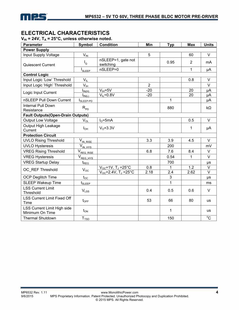
ELECTRICAL CHARACTERISTICS VIN = 24V, TA = 25°C, unless otherwise noted. Parameter Symbol Condition Min Typ Max UnitsPower Supply Input Supply Voltage VIN 5 60 V
IQ nSLEEP=1, gate not switching
0.95 2 mA Quiescent Current
ISLEEP nSLEEP=0 1 µA Control Logic Input Logic ‘Low’ Threshold VIL 0.8 V
Input Logic ‘High’ Threshold VIH 2 V IIN(H) VIH=5V -20 20 µA
Logic Input Current IIN(L) VIL=0.8V -20 20 µA
nSLEEP Pull Down Current ISLEEP-PD 1 µA
Internal Pull Down Resistance
RPD 880 kΩ
Fault Outputs(Open-Drain Outputs) Output Low Voltage VOL IO=5mA 0.5 V
Output High Leakage Current
IOH VO=3.3V 1 µA
Protection Circuit UVLO Rising Threshold VIN_RISE 3.3 3.9 4.5 V
UVLO Hysteresis VIN_HYS 200 mV
VREG Rising Threshold VREG_RISE 6.8 7.6 8.4 V
VREG Hysteresis VREG_HYS 0.54 1 V
VREG Startup Delay tREG 700 µs VOC=1V, TJ =25°C 0.8 1 1.2 V
OC_REF Threshold VOC VOC=2.4V, TJ =25°C 2.18 2.4 2.62 V
OCP Deglitch Time tOC 3 µs
SLEEP Wakeup Time tSLEEP 1 ms
LSS Current Limit Threshold
VLSS 0.4 0.5 0.6 V
LSS Current Limit Fixed Off Time
tOFF 53 66 80 us
LSS Current Limit High side Minimum On Time
tON 1 us
Thermal Shutdown TTSD 150 oC
MP6532 – 5V TO 60V, THREE PHASE BLDC MOTOR PRE-DRIVER
MP6532 Rev. 1.11 www.MonolithicPower.com 5 9/6/2015 MPS Proprietary Information. Patent Protected. Unauthorized Photocopy and Duplication Prohibited. © 2015 MPS. All Rights Reserved.
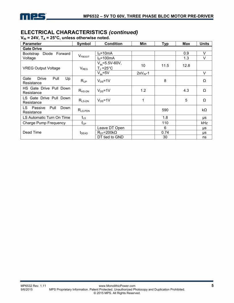
ELECTRICAL CHARACTERISTICS (continued) VIN = 24V, TA = 25°C, unless otherwise noted. Parameter Symbol Condition Min Typ Max UnitsGate Drive
ID=10mA 0.9 V Bootstrap Diode Forward Voltage
VFBOOT ID=100mA 1.3 V VIN=5.5V-60V, TJ =25°C
10 11.5 12.8 VREG Output Voltage VREG
VIN=5V 2xVIN-1 V
Gate Drive Pull Up Resistance
RUP VDS=1V 8 Ω
HS Gate Drive Pull Down Resistance
RHS-DN VDS=1V 1.2 4.3 Ω
LS Gate Drive Pull Down Resistance
RLS-DN VDS=1V 1 5 Ω
LS Passive Pull Down Resistance
RLS-PDN 590 kΩ
LS Automatic Turn On Time tLS 1.8 µs
Charge Pump Frequency fCP 110 kHz Leave DT Open 6 µs RDT=200kΩ 0.74 µs Dead Time tDEAD DT tied to GND 30 ns

MP6532 – 5V TO 60V, THREE PHASE BLDC MOTOR PRE-DRIVER
MP6532 Rev. 1.11 www.MonolithicPower.com 6 9/6/2015 MPS Proprietary Information. Patent Protected. Unauthorized Photocopy and Duplication Prohibited. © 2015 MPS. All Rights Reserved.
TYPICAL CHARACTERISTICS

MP6532 – 5V TO 60V, THREE PHASE BLDC MOTOR PRE-DRIVER
MP6532 Rev. 1.11 www.MonolithicPower.com 7 9/6/2015 MPS Proprietary Information. Patent Protected. Unauthorized Photocopy and Duplication Prohibited. © 2015 MPS. All Rights Reserved.
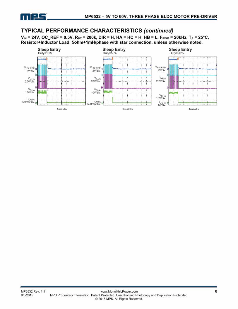
TYPICAL PERFORMANCE CHARACTERISTICS VIN = 24V, OC_REF = 0.5V, RDT = 200k, DIR = H, HA = HC = H, HB = L, FPWM = 20kHz, TA = 25°C, Resistor+Inductor Load: 5ohm+1mH/phase with star connection, unless otherwise noted.
Power Ramp UpDuty=10%
Power Ramp UpDuty=50%
Sleep RecoveryDuty=10%
Power Ramp UpDuty=90%
Sleep RecoveryDuty=90%
Sleep RecoveryDuty=50%
VGHA20V/div.
VGLA10V/div.
VSHA20V/div.
IOUTA100mA/div.
VIN10V/div.
VGHA20V/div.
VSHA20V/div.
IOUTA100mA/div.
VnSLEEP2V/div.VGHA
20V/div.
VSHA20V/div.
IOUTA100mA/div.
VnSLEEP2V/div.VGHA
20V/div.
VSHA20V/div.
IOUTA500mA/div.
VnSLEEP2V/div.VGHA
20V/div.
VSHA20V/div.
IOUTA1A/div.
VIN10V/div.
VGHA20V/div.
VSHA20V/div.
IOUTA500mA/div.
VIN10V/div.
VGHA20V/div.
VSHA20V/div.
IOUTA1A/div.
VGHA20V/div.
VGLA10V/div.
VSHA20V/div.
IOUTA500mA/div.
VGHA20V/div.
VGLA10V/div.
VSHA20V/div.
IOUTA500mA/div.
Steady StateDuty=10%
Steady StateDuty=50%
Steady StateDuty=90%
MP6532 – 5V TO 60V, THREE PHASE BLDC MOTOR PRE-DRIVER
MP6532 Rev. 1.11 www.MonolithicPower.com 8 9/6/2015 MPS Proprietary Information. Patent Protected. Unauthorized Photocopy and Duplication Prohibited. © 2015 MPS. All Rights Reserved.
TYPICAL PERFORMANCE CHARACTERISTICS (continued) VIN = 24V, OC_REF = 0.5V, RDT = 200k, DIR = H, HA = HC = H, HB = L, FPWM = 20kHz, TA = 25°C, Resistor+Inductor Load: 5ohm+1mH/phase with star connection, unless otherwise noted.
VnSLEEP2V/div.
VGHA20V/div.
VSHA10V/div.
IOUTA100mA/div.
VnSLEEP2V/div.
VGLA20V/div.
VSHA10V/div.
IOUTA500mA/div.
VnSLEEP2V/div.
VGLA20V/div.
VSHA10V/div.
IOUTA1A/div.
Sleep EntryDuty=10%
Sleep EntryDuty=50%
Sleep EntryDuty=90%

MP6532 – 5V TO 60V, THREE PHASE BLDC MOTOR PRE-DRIVER
MP6532 Rev. 1.11 www.MonolithicPower.com 9 9/6/2015 MPS Proprietary Information. Patent Protected. Unauthorized Photocopy and Duplication Prohibited. © 2015 MPS. All Rights Reserved.
PIN FUNCTIONS QFN28 Pin #
TSSOP-28 Pin #
Name Description
1 26 VIN Input supply voltage. 2 27 CPA Charge pump capacitor connect terminal. 3 28 CPB Charge pump capacitor connect terminal. 4 1 VREG Gate drive supply output. 5 2 BSTA Bootstrap output phase A. 6 3 SHA High-side source connection phase A. 7 4 GHA High-side gate drive phase A. 8 5 GLA Low-side gate drive phase A. 9 6 BSTB Bootstrap output phase B.
10 7 SHB High-side source connection phase B. 11 8 GHB High-side gate drive phase B. 12 9 GLB Low-side gate drive phase B. 13 10 BSTC Bootstrap output phase C. 14 11 SHC High-side source connection phase C. 15 12 GHC High-side gate drive phase C. 16 13 GLC Low-side gate drive phase C. 17 14 LSS Low-side source connection. 18 15 HC Hall-sensor input, phase C. 19 16 HB Hall-sensor input, phase B. 20 17 HA Hall-sensor input, phase A. 21 18 nBRAKE An active-low logic input for a braking function. 22 19 PWM External PWM control for speed/torque. 23 20 DIR A logic input to determine the direction of motor torque output.
24 21 nFAULT Fault indication. Open-drain output. nFAULT is logic low when in a fault condition.
25 22 nSLEEP Sleep mode input. Logic low to enter low-power sleep mode. Float to enable.
26 23 OC_REF Over-current protection reference input. 27 24 DT Dead time setting. 28 25 GND Ground.
MP6532 – 5V TO 60V, THREE PHASE BLDC MOTOR PRE-DRIVER
MP6532 Rev. 1.11 www.MonolithicPower.com 10 9/6/2015 MPS Proprietary Information. Patent Protected. Unauthorized Photocopy and Duplication Prohibited. © 2015 MPS. All Rights Reserved.
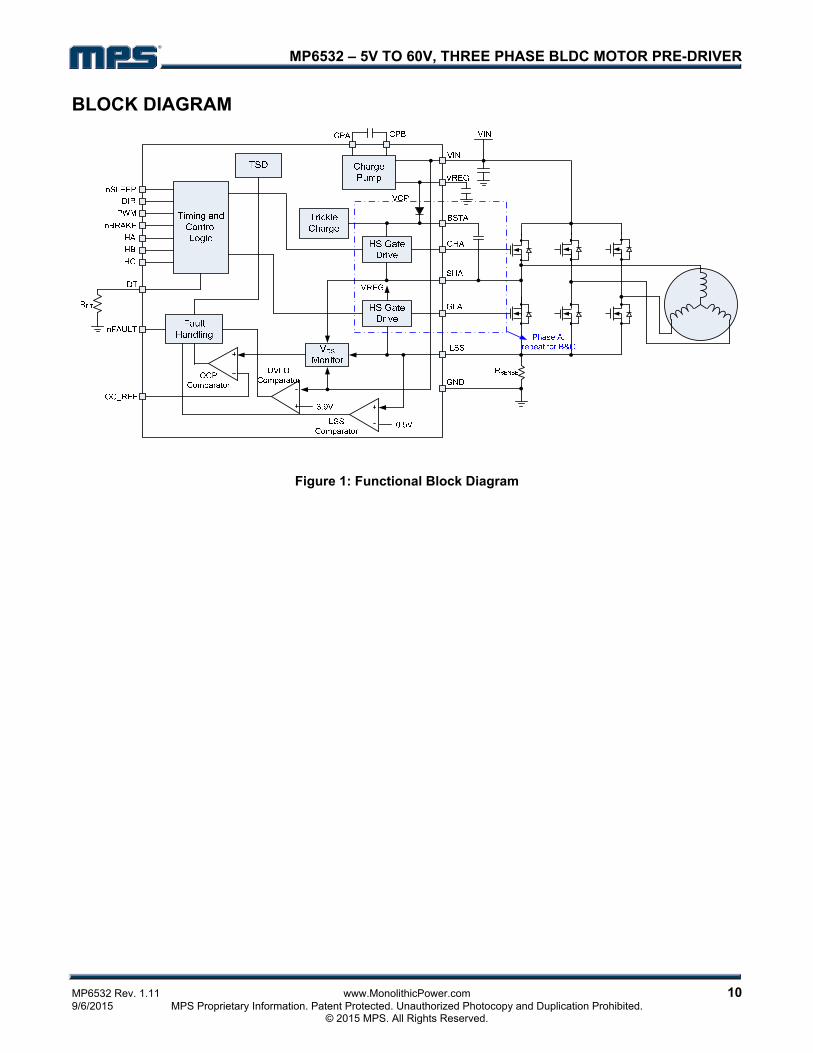
BLOCK DIAGRAM
Figure 1: Functional Block Diagram
MP6532 – 5V TO 60V, THREE PHASE BLDC MOTOR PRE-DRIVER
MP6532 Rev. 1.11 www.MonolithicPower.com 11 9/6/2015 MPS Proprietary Information. Patent Protected. Unauthorized Photocopy and Duplication Prohibited. © 2015 MPS. All Rights Reserved.
OPERATION The MP6532 is a three-phase BLDC motor pre-driver that can drive three half bridges with a 0.8A source and a 1A sink current capability over a wide input voltage range of 5V to 60V. It is designed for use in battery-powered equipment. The MP6532 features a low-power sleep mode, which disables the device and draws a very low supply current.
The MP6532 provides several flexible functions, such as adjustable dead-time control and over-current protection, which allow the device to cover a wide range of application fields.
nFAULT
nFAULT reports to the system when a fault condition (such as OCP and OTP) is detected. nFAUlt can be an open-drain output, and it is driven low once a fault condition occurs. If the fault condition is released, nFAULT is pulled high by an external pull-up resistor.
Over-Current Protection
To protect the power stage from damage due to high currents, a VDS sensing circuitry is implemented in the MP6532. Based on RDS-ON of the power MOSFETs and the maximum allowed IDS, a voltage threshold can be calculated which triggers the OC protection feature when exceeded. This voltage threshold level is programmable through the OC_REF terminal by applying an external reference voltage with a DAC. Once an OCP event is detected, MP6532 will enter a latched fault state and disable all functions. MP6532 will stay latched off until it is reset by nSLEEP or UVLO.
Motor Startup Current Limit
MP6532 limits the motor startup current by monitoring the voltage at LSS pin. When the voltage at LSS exceeds the current limit threshold of 0.5V, the high side will turn off and the corresponding low side turns on for a fixed off time. After the fixed off time, the high side will turn back on and the cycle repeats until LSS no longer exceeds the current limit threshold. The current limit level is selected by the value of the current sense resistor at LSS pin.
OCP Deglitch Time
Usually, there is a current spike during the switching transition due to the body diode’s reverse-recovery current or the distributed inductance or capacitance. This current spike requires filtering to prevent it from erroneously triggering OCP and shutting down the external MOSFET. An internal fixed deglitch time (tOC) blanks the output of the VDS monitor when the outputs are switched (which is also the minimum on time for the MOSFET).
Dead Time Adjustment
To prevent shoot-through in any phase of the bridge, it is necessary to have a dead time (tDEAD) between a high- or low-side turn-off and the next complementary turn-on event. The dead time for all three phases is set by a single dead-time resistor (RDT) between DT and ground with Equation(1): tDEAD(nS) = 3.7*R(kΩ) (1) If DT is tied to GND directly, an internal minimum dead time (30ns) will be applied. Leaving DT open generates a 6µs dead time.
Input UVLO Protection
If at any time the voltage on VIN falls below the under-voltage lockout threshold voltage, all circuitry in the device is disabled and the internal logic will be reset. Operation will resume when VIN rises above the UVLO threshold.
Thermal Shutdown
If the die temperature exceeds safe limits, the MP6532 enters a latched fault state similar to an OCP event, and nFAULT is driven low. Only resetting by nSLEEP or UVLO will unlatch the device from an OTP fault lockout.
Input Logic
Driving nSLEEP low will put the device into a low-power sleep state. In this state, all the internal circuits are disabled. All inputs are ignored when nSLEEP is active low. When exiting sleep mode, a brief time period (approximately 1ms) must pass before issuing a PWM command. This time period allows the internal circuitry to stabilize.
MP6532 – 5V TO 60V, THREE PHASE BLDC MOTOR PRE-DRIVER
MP6532 Rev. 1.11 www.MonolithicPower.com 12 9/6/2015 MPS Proprietary Information. Patent Protected. Unauthorized Photocopy and Duplication Prohibited. © 2015 MPS. All Rights Reserved.
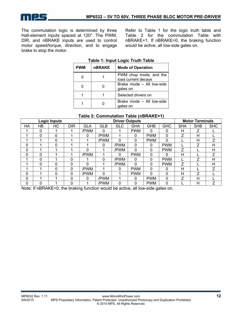
The commutation logic is determined by three Hall-element inputs spaced at 120°. The PWM, DIR, and nBRAKE inputs are used to control motor speed/torque, direction, and to engage brake to stop the motor.
Refer to Table 1 for the logic truth table and Table 2 for the commutation Table with nBRAKE=1. If nBRAKE=0, the braking function would be active, all low-side gates on.
Table 1: Input Logic Truth Table
PWM nBRAKE Mode of Operation
0 1 PWM chop mode, and the load current decays
0 0 Brake mode – All low-side gates on
1 1 Selected drivers on
1 0 Brake mode – All low-side gates on
Table 2: Commutation Table (nBRAKE=1)
Logic Inputs Driver Outputs Motor Terminals HA HB HC DIR GLA GLB GLC GHA GHB GHC SHA SHB SHC1 0 1 1 /PWM 0 1 PWM 0 0 H Z L 1 0 0 1 0 /PWM 1 0 PWM 0 Z H L 1 1 0 1 1 /PWM 0 0 PWM 0 L H Z 0 1 0 1 1 0 /PWM 0 0 PWM L Z H 0 1 1 1 0 1 /PWM 0 0 PWM Z L H 0 0 1 1 /PWM 1 0 PWM 0 0 H L Z 1 0 1 0 1 0 /PWM 0 0 PWM L Z H 1 0 0 0 0 1 /PWM 0 0 PWM Z L H 1 1 0 0 /PWM 1 0 PWM 0 0 H L Z 0 1 0 0 /PWM 0 1 PWM 0 0 H Z L 0 1 1 0 0 /PWM 1 0 PWM 0 Z H L 0 0 1 0 1 /PWM 0 0 PWM 0 L H Z
Note: If nBRAKE=0, the braking function would be active, all low-side gates on.
MP6532 – 5V TO 60V, THREE PHASE BLDC MOTOR PRE-DRIVER
MP6532 Rev. 1.11 www.MonolithicPower.com 13 9/6/2015 MPS Proprietary Information. Patent Protected. Unauthorized Photocopy and Duplication Prohibited. © 2015 MPS. All Rights Reserved.
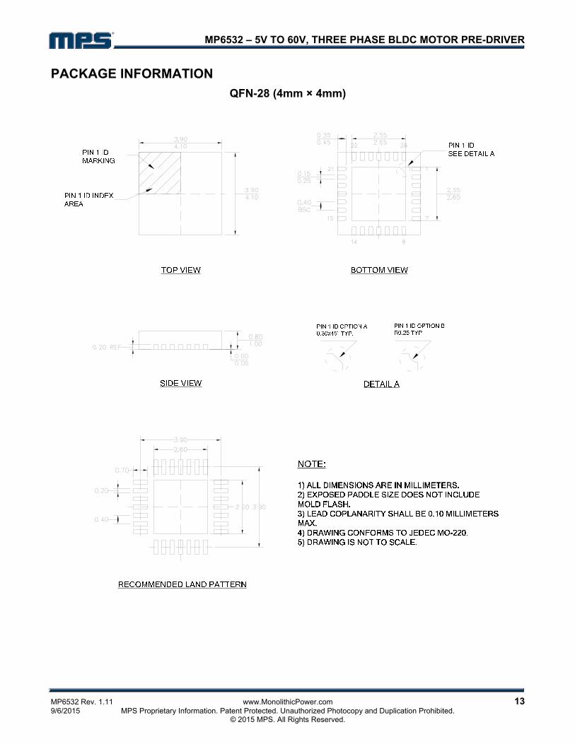
PACKAGE INFORMATION
QFN-28 (4mm × 4mm)
MP6532 – 5V TO 60V, THREE PHASE BLDC MOTOR PRE-DRIVER
NOTICE: The information in this document is subject to change without notice. Users should warrant and guarantee that third party Intellectual Property rights are not infringed upon when integrating MPS products into any application. MPS will not assume any legal responsibility for any said applications.
MP6532 Rev. 1.11 www.MonolithicPower.com 14 9/6/2015 MPS Proprietary Information. Patent Protected. Unauthorized Photocopy and Duplication Prohibited. © 2015 MPS. All Rights Reserved.
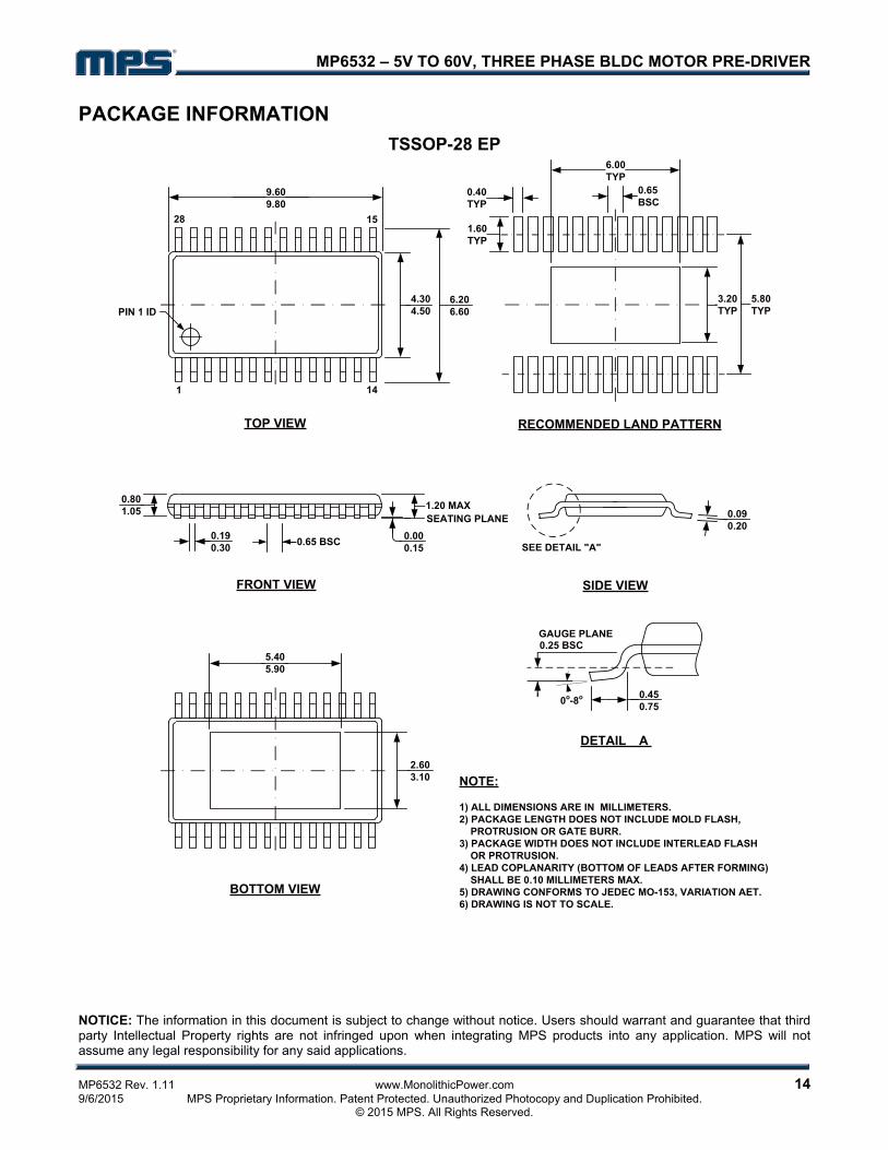
PACKAGE INFORMATION
TSSOP-28 EP
SIDE VIEW
NOTE:
1) ALL DIMENSIONS ARE IN MILLIMETERS.2) PACKAGE LENGTH DOES NOT INCLUDE MOLD FLASH, PROTRUSION OR GATE BURR.3) PACKAGE WIDTH DOES NOT INCLUDE INTERLEAD FLASH OR PROTRUSION.4) LEAD COPLANARITY (BOTTOM OF LEADS AFTER FORMING) SHALL BE 0.10 MILLIMETERS MAX.5) DRAWING CONFORMS TO JEDEC MO-153, VARIATION AET.6) DRAWING IS NOT TO SCALE.
DETAIL A
0.450.75
0o-8o
0.25 BSCGAUGE PLANE
9.609.80
PIN 1 ID4.304.50
6.206.60
1 14
1528
TOP VIEW
0.090.20
SEE DETAIL "A"
BOTTOM VIEW
2.603.10
5.405.90
0.190.30
SEATING PLANE
0.65 BSC
0.801.05 1.20 MAX
0.000.15
FRONT VIEW
RECOMMENDED LAND PATTERN
5.80TYP
1.60TYP
0.40 TYP
0.65 BSC
3.20TYP
6.00TYP

Mouser Electronics
Authorized Distributor
Click to View Pricing, Inventory, Delivery & Lifecycle Information: Monolithic Power Systems (MPS):
MP6532GR-P