m.sc. thesis investigation of the electrical performance
TRANSCRIPT
i
M.Sc. Thesis
Investigation of the electrical performance of epoxy/ silicon rubber interface
Design of a standardized 145 kV inner-cone GIS cable termination
Sanjay Ganeshan

ii
iii
Investigation of the electrical performance of epoxy/ silicon rubber interface
Design of a standardized 145 kV inner-cone GIS cable
termination
by
Sanjay Ganeshan
in partial fulfilment of the requirements for the degree of
Master of Science
in Electrical Engineering
at the Delft University of Technology, to be defended publicly on Friday July 27, 2018 at 10:00 AM
Student number : 4614275
Project duration : November 8, 2017 – July 27, 2018 Thesis supervisors: Prof. dr. ir. Armando Rodrigo Mor, Daily Supervisor/ TU Delft Ir. Panagiotis Tsakonas, Company Supervisor/ Prysmian Group Thesis committee : Prof. dr. Rob Ross, Full Professor, TU Delft Prof. dr. ir. Armando Rodrigo Mor, Assistant Professor, TU Delft Prof. dr. ir. Milos Cvetkovic, External Expert, TU Delft
This thesis is confidential and cannot be made public until July 31, 2020. Certain parts of this thesis are redacted due to confidentiality agreements.
An electronic version of this thesis is available at https://repository.tudelft.nl.

iv

v
நன்றி மறப்பது நன்றன்று நன்றல்லது
அன்றற மறப்பது நன்று.
குறள்: #108
பால்: அறத்துப்பால்
இயல்: இல்லறவியல்
அதிகாரம்: செய்ந்நன்றி அறிதல்
Translation
Never forget the (good) deeds that someone did to you,
But, forget the (bad) deeds immediately
The above verse is a couplet from the Thirukkural, a classic Tamil language text consisting of 1,330 couplets,
dealing with the everyday virtues of an individual. Considered one of the greatest works ever written on ethics and
morality, chiefly secular ethics, it is known for its universality and non-denominational nature. It was authored by
Valluvar, also known in full as Thiruvalluvar. The text has been dated variously from 300 BCE to 7th century CE.

vi
vii
Acknowledgements
Firstly, I would like to thank all my Professors from TU Delft. Each of their courses have
contributed in to the betterment of this thesis. I would also like to thank Prysmian Group for
giving me this unique opportunity to design their first standardized inner-cone GIS cable
termination.
I would like to thank my TU Delft daily supervisor, Dr. Armando Rodrigo Mor for his
constant support and encouragement during my entire Master program. I owe my gratitude to
him for helping me to balance between the academic and company perspectives of the thesis. His
motivation and innovative ideas helped a lot during this thesis work. I would also like to take this
opportunity to express my gratitude to Prof. Dr. Rob Ross and Prof. Peter Vaessen
for sharing their rich technical experience and expertise during the entire course of this thesis.
Their insights helped me a lot in every stage of this thesis.
I would like to profusely thank my company supervisor Ir. Panos Tsakonas for his
advice, guidance and supervision to help me get accustomed to the finite element modelling from
scratch. His appreciation and ideas helped me a lot. I would also like to take this opportunity to
thank Dr. Riccardo Bodega for his constant guidance and encouragement during my thesis. I
deeply value his support and motivation during my work. I would also like to sincerely thank my
colleagues from Prysmian Group (Delft) for extending their warm hospitality and helping me at
different stages of this thesis work.
I would like to express my heartfelt gratitude to Paul van Nes, Radek Heller,
Remko Koornneef and Wim Termorshuizen from The TU Delft High Voltage Laboratory, for
their warm hospitality and untiring assistance especially during experimental stage of this thesis.
I would like to express my sincere thanks to all my friends and well-wishers who helped
me during different stages of my study.
Last, but never the least, I would like to dedicate this thesis work to my beloved parents
and my dear brother for their immense support during my study and Master thesis.
Sanjay Ganeshan Delft, July 2018

viii
ix
Table of contents
Table of contents ......................................................................................................................... ix
List of figures .............................................................................................................................. xi
List of tables ............................................................................................................................... xv
Glossary ................................................................................................................................... xvii
Abstract ..................................................................................................................................... xix
1. Introduction ............................................................................................................................. 1
1.1 Introduction ......................................................................................................................... 2
1.2 Motivation ........................................................................................................................... 2
1.3 State of the art- GIS terminations ........................................................................................ 3
1.4 State of the art – Epoxy/ silicon rubber interface study ...................................................... 5
1.5 Scope of the thesis ............................................................................................................... 5
1.6 Problem statement ............................................................................................................... 6
1.7 Research goals ..................................................................................................................... 6
1.8 Thesis layout ....................................................................................................................... 6
2. Literature study ....................................................................................................................... 9
2.1 Solid | solid interface study ............................................................................................... 10
2.2 Epoxy/ SiR interface study ................................................................................................ 17
3. Hyperelastic material modelling of silicon rubber ............................................................. 21
3.1 Stress – strain curves ......................................................................................................... 22
3.2 Need for hyperelastic material modelling ......................................................................... 23
3.3 Types of hyperelastic material modelling ......................................................................... 27
3.4 Mechanical tests of SiR ..................................................................................................... 29
3.5 Determining the type of material model ........................................................................... 33
3.6 Conclusions ....................................................................................................................... 34
4. Design of test setup for interfacial study ............................................................................. 35
4.1 Learning outcomes from literature study .......................................................................... 36
4.2 Test setup – draft designs .................................................................................................. 37
4.3 Preliminary testing- sizing of samples and test setup ....................................................... 43
4.4 Design of test setup ........................................................................................................... 45
4.5 Relationship between weight and interfacial pressure ...................................................... 53
4.6 Summary ........................................................................................................................... 53

x
5. Experimental study of epoxy/ silicon rubber interface ...................................................... 57
5.1 Test cell and test preparation ............................................................................................. 58
5.2 AC Breakdown tests .......................................................................................................... 60
5.3 AC Breakdown tests with oil at the interface .................................................................... 69
5.4 AC breakdown tests with scratch on epoxy ...................................................................... 75
5.5 AC breakdown tests with heated samples ......................................................................... 80
5.6 Lightning Impulse tests ..................................................................................................... 86
5.7 Summary of experimental testing ..................................................................................... 90
6. Design of GIS termination .................................................................................................... 93
6.1 CIGRE JWG design .......................................................................................................... 94
6.2 Design ‘A’ ......................................................................................................................... 96
6.3 Design ‘B’ ......................................................................................................................... 99
6.4 Analysis of proposed designs .......................................................................................... 102
6.5 Summary ......................................................................................................................... 111
7. Conclusions and future scope ............................................................................................. 113
7.1 Conclusions ..................................................................................................................... 114
7.2 Answers to research goals/ questions .............................................................................. 116
7.3 Recommendations for future work .................................................................................. 117
Bibliography .............................................................................................................................. 119
xi
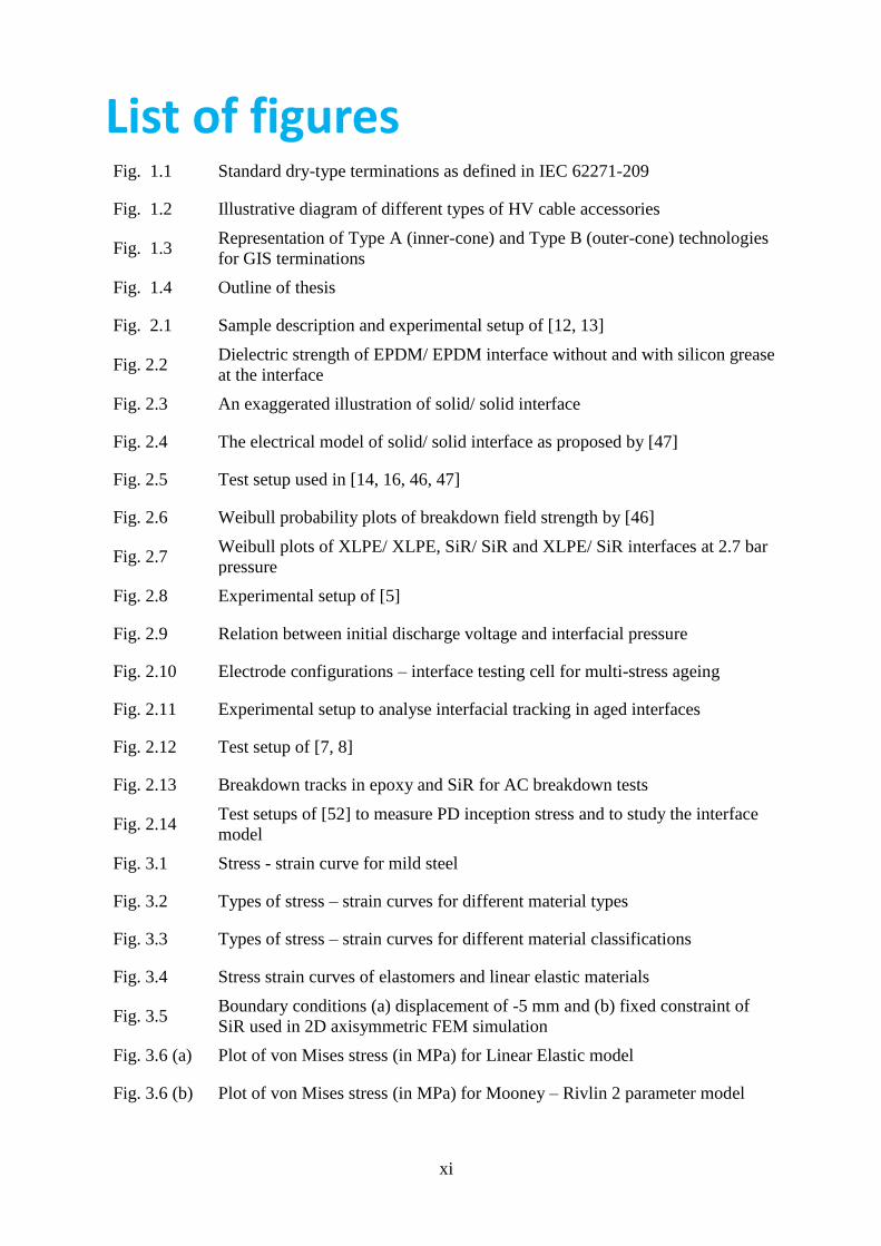
List of figures Fig. 1.1 Standard dry-type terminations as defined in IEC 62271-209
Fig. 1.2 Illustrative diagram of different types of HV cable accessories
Fig. 1.3 Representation of Type A (inner-cone) and Type B (outer-cone) technologies
for GIS terminations
Fig. 1.4 Outline of thesis
Fig. 2.1 Sample description and experimental setup of [12, 13]
Fig. 2.2 Dielectric strength of EPDM/ EPDM interface without and with silicon grease
at the interface
Fig. 2.3 An exaggerated illustration of solid/ solid interface
Fig. 2.4 The electrical model of solid/ solid interface as proposed by [47]
Fig. 2.5 Test setup used in [14, 16, 46, 47]
Fig. 2.6 Weibull probability plots of breakdown field strength by [46]
Fig. 2.7 Weibull plots of XLPE/ XLPE, SiR/ SiR and XLPE/ SiR interfaces at 2.7 bar
pressure
Fig. 2.8 Experimental setup of [5]
Fig. 2.9 Relation between initial discharge voltage and interfacial pressure
Fig. 2.10 Electrode configurations – interface testing cell for multi-stress ageing
Fig. 2.11 Experimental setup to analyse interfacial tracking in aged interfaces
Fig. 2.12 Test setup of [7, 8]
Fig. 2.13 Breakdown tracks in epoxy and SiR for AC breakdown tests
Fig. 2.14 Test setups of [52] to measure PD inception stress and to study the interface
model
Fig. 3.1 Stress - strain curve for mild steel
Fig. 3.2 Types of stress – strain curves for different material types
Fig. 3.3 Types of stress – strain curves for different material classifications
Fig. 3.4 Stress strain curves of elastomers and linear elastic materials
Fig. 3.5 Boundary conditions (a) displacement of -5 mm and (b) fixed constraint of
SiR used in 2D axisymmetric FEM simulation
Fig. 3.6 (a) Plot of von Mises stress (in MPa) for Linear Elastic model
Fig. 3.6 (b) Plot of von Mises stress (in MPa) for Mooney – Rivlin 2 parameter model
xii
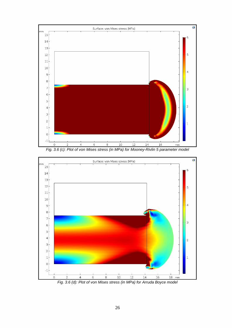
Fig. 3.6 (c) Plot of von Mises stress (in MPa) for Mooney – Rivlin 5 parameter model
Fig. 3.6 (d) Plot of von Mises stress (in MPa) for Arruda Boyce model
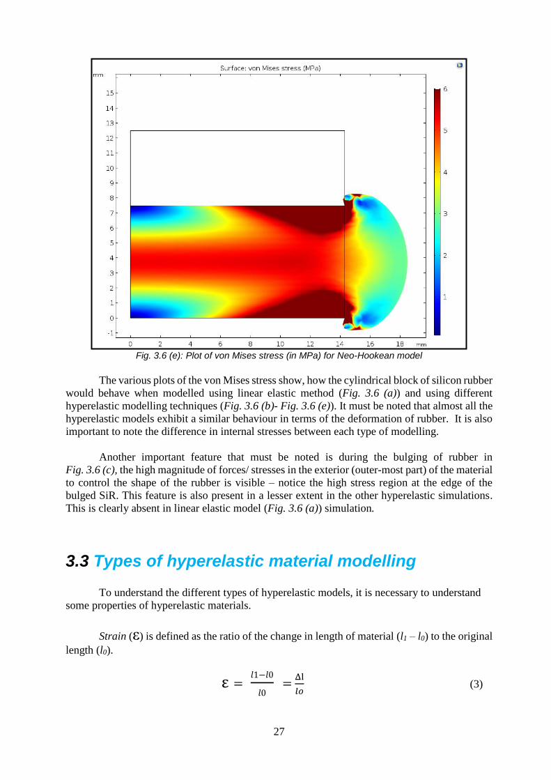
Fig. 3.6 (e) Plot of von Mises stress (in MPa) for Neo - Hookean model
Fig. 3.7 Types of mechanical tests performed on rubber
Fig. 3.8 (a) Test setup for tensile strength measurements
Fig. 3.8 (b) Dumbbell shaped samples
Fig. 3.9 Median tensile stress – strain plots at 23°C and 80°C
Fig. 3.10 Median compressive stress – strain plots at 23°C and 80°C
Fig. 3.11 Median stress – strain plots at 23°C and 80°C
Fig. 3.12 Screenshot of ANSYS workbench for hyperelastic material data curve –
fitting
Fig. 4.1 Draft setup #1 – components
Fig. 4.2 Draft setup #1 – Tangential electric field at the interface
Fig. 4.3 Draft setup #2 – components
Fig. 4.4 Draft setup #2 – Tangential electric field at the interface
Fig. 4.5 Draft setup #3 – components
Fig. 4.6 Draft setup #3 – Electric field at the interface
Fig. 4.7 Draft setup #4 – components
Fig. 4.8 Draft setup #4 – Electric field at the interface
Fig. 4.9 Preliminary testing for sample dimensions – two SiR samples
Fig. 4.10 Preliminary testing for sample dimensions – slit in SiR
Fig. 4.11 Samples of silicon rubber and epoxy
Fig. 4.12 3D drawing of test setup
Fig. 4.13 Base plate [part #1]
Fig. 4.14 Sample holder (bottom) [part #2]
Fig. 4.15 (a) Sample holder (top) [part #3] – top view
Fig. 4.15 (b) Sample holder (top) [part #3] – bottom view
Fig. 4.16 Electrode holder(s) [part #4]
Fig. 4.17 Guiding rod(s) [part #5]

xiii
Fig. 4.18 (a) Weight carrying plate [part #6] – top view
Fig. 4.18 (b) Weight carrying plate [part #6] – bottom view
Fig. 4.19 Stainless steel electrode and the entire electrode assembly
Fig. 4.20 Zoomed image of space between the upper and lower sample holders
Fig. 4.21 Fully assembled test setup
Fig. 5.1 Test setup for AC breakdown testing
Fig. 5.2 Test setup for lightning impulse testing
Fig. 5.3 Oval shaped hand – cut semi-conductive tapes
Fig. 5.4 Flowchart – AC breakdown test
Fig. 5.5 AC breakdown path – 0.2 bar
Fig. 5.6 AC breakdown path – 0.5 bar
Fig. 5.7 AC breakdown path – 1 bar
Fig. 5.8 AC breakdown path – 1.5 bar
Fig. 5.9 AC breakdown path – 2 bar
Fig. 5.10 AC breakdown field strength - summary
Fig. 5.11 Silicon oil used as lubricant during installation
Fig. 5.12 Silicon grease used to prevent inner-side flashovers
Fig. 5.13 Flowchart – AC breakdown test with oil at the interface
Fig. 5.14 AC breakdown field strength with oil at the interface – summary
Fig. 5.15 Flowchart – AC breakdown test with scratch on epoxy
Fig. 5.16 AC breakdown path with scratch on the epoxy – 1 bar
Fig. 5.17 AC breakdown path with scratch on the epoxy – 2 bar
Fig. 5.18 AC breakdown field strength with scratch on epoxy – summary
Fig. 5.19 Heating of epoxy and silicon rubber samples
Fig. 5.20 Flowchart – AC breakdown test with heated samples
Fig. 5.21 AC breakdown path of heated samples – 0.5 bar
Fig. 5.22 AC breakdown path of heated samples – 1 bar
Fig. 5.23 AC breakdown path of heated samples – 2 bar
xiv
Fig. 5.24 AC breakdown field strength with heated samples - summary
Fig. 5.25 Flowchart – LI breakdown test
Fig. 5.26 Lightning impulse breakdown field strength – summary
Fig. 5.27 AC and lightning impulse breakdown tests - summary
Fig. 6.1 CIGRE JWG B1 – B3.49 standard for 145 kV inner cone GIS termination
Fig. 6.2 Design ‘A’ – with aluminium extension rod
Fig. 6.3 Design ‘A’ of 145 kV inner-cone termination
Fig. 6.4 Design ‘A’ – with aluminium extension rod and stress cone
Fig. 6.5 Design ‘B’ – with aluminium extension rod
Fig. 6.6 Design ‘B’ of 145 kV inner-cone termination
Fig. 6.7 Design ‘B’ – with aluminium extension rod and cable locking adapter
Fig. 6.8 (a) Design ‘A’ – Normal electric field in kV/mm at 650 kV (BIL)
Fig. 6.8 (b) Design ‘B’ – Normal electric field in kV/mm at 650 kV (BIL)
Fig. 6.9 Tangential electric field plot of proposed designs – epoxy/ silicon rubber
interface at BIL – 650 kV
Fig. 6.10 Tangential electric field plot of existing accessories – epoxy/ silicon rubber
interface at respective BIL voltages (kV/mm)
Fig. 6.11 Tangential electric field plot of proposed designs – XLPE/ silicon rubber
interface at BIL – 650 kV
Fig. 6.12 Tangential electric field plot of existing accessories – XLPE/ silicon rubber
interface at respective BIL voltages (kV/mm)
Fig. 6.13 Tangential electric field plot of proposed designs – epoxy/ SF6 interface at
BIL – 650 kV
Fig. 6.14 Tangential electric field plot of existing accessories – epoxy/ SF6 interface at
respective BIL voltages (kV/mm)
Fig. 6.15 Boundary conditions for mechanical FEM simulations
Fig. 6.16 Design ‘A’ – plot of pressure distribution (in bar) for a spring force of 5 bar
Fig. 6.17 Design ‘B’ – plot of pressure distribution (in bar) for a spring force of 5 bar
Fig. 6.18 Comparative plot of pressure distribution (in bar) at the epoxy/ silicon rubber
interface for a spring force of 5 bar
xv
List of tables Table 3.1 Comparison of linear elastic and hyperelastic materials
Table 4.1 Summary of draft test setup designs
Table 4.2 Relation between applied weights (kg) and interfacial pressure (bar)
Table 5.1 AC breakdown results – 0.2 bar
Table 5.2 AC breakdown results – 0.5 bar
Table 5.3 AC breakdown results – 1 bar
Table 5.4 AC breakdown results – 1.5 bar
Table 5.5 AC breakdown results – 2 bar
Table 5.6 AC breakdown with oil at the interface – 0.5 bar
Table 5.7 AC breakdown with oil at the interface – 1 bar
Table 5.8 AC breakdown with scratch on epoxy at 1 bar – results
Table 5.9 AC breakdown with scratch on epoxy at 2 bar – results
Table 5.10 AC breakdown with heated samples at 0.5 bar - results
Table 5.11 AC breakdown with heated samples at 1 bar - results
Table 5.12 AC breakdown with heated samples at 2 bar - results
Table 5.13 Lightning Impulse test – 1 bar
Table 6.1 Comparative summary of electrical performance

xvi

xvii
Glossary
XLPE Cross Linked Poly-Ethylene
SiR Silicon Rubber
EPDM Ethylene Propylene Diene Monomer rubber
EPR Ethylene Propylene Rubber
PD Partial Discharge
LI Lightning Impulse
BD breakdown
BIL Basic Impulse Level

xviii
xix
Abstract
The CIGRE B1 – B3.49 JWG defined a standardised 145 kV inner-cone GIS cable
termination design. This standardisation allows the creation of new common interface insulators.
This would eliminate the planning hurdles due to the fact that the cable system is not usually
defined at the time of switchgear manufacture. The new design also requires a detailed study to
find the relation between interfacial pressure and electrical performance of the epoxy/ silicon
rubber interface.
The first step is to design and build a test setup to study the epoxy/ silicon rubber interface.
Next, AC breakdown and lightning impulse tests are carried out. Additional AC breakdown
testing with oil at the interface, defects on epoxy and heated samples are also carried out. The
relation between interfacial pressure and electric field strength of the interface is found and
documented. The effects of lubricant, defects and heat is used to further characterise the interface.
Simultaneously, the silicon rubber is modelled using hyperelastic material modelling techniques.
The results from the tests and FEM models are used to propose two new designs of the
145 kV inner-cone GIS cable termination. The high repeatability of breakdown values and
distinct features of this test setup have prompted the sharing of the experimental setup and results
through an IEEE publication.

0

1
1. Introduction
In this chapter, the first section introduces the topic of the M.Sc. thesis, followed by the
motivation. The third and fourth sections explain the current developments/ trends regarding GIS
cable terminations and interface study respectively. The fifth section elaborates on the scope of
this thesis. The subsequent sections elaborate on the problem statement, research goals and the
layout of this thesis report.
2
1.1 Introduction
The topic of this M.Sc. thesis is “Design of a standardized inner-cone 145 kV GIS
cable termination – Analysis of the epoxy/ silicon rubber interface”.
The main aim of this thesis is to find and document the relation between electrical
performance of epoxy/ silicon rubber interface with respect to interfacial pressure. This
knowledge is then used as a reference to design, a 145 kV inner-cone GIS cable termination
in accordance with CIGRE JWG B1-B3.49 recommendations.
1.2 Motivation
Considering the large number of substations and practical planning difficulties because
the cable system is usually not defined at the time of switchgear manufacturing. This gave rise
to a CIGRE JWG B1-B3.49 comprising of experts from CIGRE B1 (cables) and CIGRE B3
(switchgear). The duty of this JWG was to explore the possibility of a standardized common
interface insulator for the dry type, plug-in termination such that it could be supplied
independently from the remaining termination components. In other words, the GIS manufacturer
will have the possibility to complete the GIS manufacturing independent from the cable and
termination supplier.
Following the CIGRE JWG study, for a certain range of application a standardized
interface is recommended. This means that cable manufactures will need to design new dry-type
and plug-in cable termination that fits the standardized interface. At the other end, it is
important that the new dry-type and plug-in cable termination maintains the characteristics the
cable manufacturers consider necessary for their specific design.
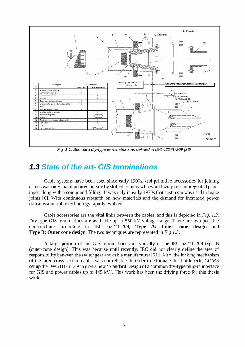
The interface between silicon rubber and epoxy has a lot of significance in the design of
cable accessories. This is because the interface forms the boundary of the ‘limit of supply/
responsibilty’ of the cable termination manufacturer and the switchgear manufacturer (refer
Fig. 1.1). With the emerging trend of standardized common interface insulators for dry type
terminations, this gains further importance. For this reason, the effect of non-electrical
parameters like interfacial pressure, on the electric strength of the epoxy/ rubber interface must
be examined before defining the final design of the termination. An experimental approach is
necessary to find out this relationship.
After defining the final geometry of the termination, further checks/ tests need to be
performed, before and after production of the first prototypes. The results of these tests will
validate the design of the termination before releasing it for further short and long term
qualification
3
Fig. 1.1: Standard dry-type terminations as defined in IEC 62271-209 [23]
1.3 State of the art- GIS terminations
Cable systems have been used since early 1900s, and primitive accessories for joining
cables was only manufactured on-site by skilled jointers who would wrap pre-impregnated paper
tapes along with a compound filling. It was only in early 1970s that cast resin was used to make
joints [6]. With continuous research on new materials and the demand for increased power
transmission, cable technology rapidly evolved.
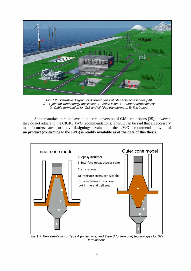
Cable accessories are the vital links between the cables, and this is depicted in Fig. 1.2.
Dry-type GIS terminations are available up to 550 kV voltage range. There are two possible
constructions according to IEC 62271-209, Type A: Inner cone design and
Type B: Outer cone design. The two techniques are represented in Fig 1.3.
A large portion of the GIS terminations are typically of the IEC 62271-209 type B
(outer-cone design). This was because until recently, IEC did not clearly define the area of
responsibility between the switchgear and cable manufacturer [21]. Also, the locking mechanism
of the large cross-section cables was not reliable. In order to eliminate this bottleneck, CIGRE
set up the JWG B1-B3.49 to give a new ‘Standard Design of a common dry-type plug-in interface
for GIS and power cables up to 145 kV’. This work has been the driving force for this thesis
work.
4
Fig. 1.2: Illustrative diagram of different types of HV cable accessories [38] (A- Y joint for wind energy application; B- cable joints; C- outdoor terminations;
D- Cable termination for GIS and oil-filled transformers; E- link boxes)
Some manufacturers do have an inner-cone version of GIS terminations [35]; however,
they do not adhere to the CIGRE JWG recommendations. Thus, it can be said that all accessory
manufacturers are currently designing/ evaluating the JWG recommendations, and
no product (confirming to the JWG) is readily available as of the date of this thesis.
Fig. 1.3: Representation of Type A (inner-cone) and Type B (outer-cone) technologies for GIS
terminations
5
1.4 State of the art – Epoxy/ silicon rubber interface study
The interface of any two materials is always considered as the weakest point in high
voltage design [9, 28, 52]. This is due to the fact that the tangential component of the electric
field may have high values here and thus get highly stressed. Also factors like interfacial pressure,
temperature and material properties play an important role in the electrical performance of the
interface.
Interface studies have been carried out for different materials and with/ without other
variable parameters like temperature, oil, grease, pressure, etc., A few studies have been carried
out regarding epoxy/ silicon rubber interface. A detailed overview of different studies/ research
in literature is provided in Chapter 2.
However, it is worth mentioning that no standard/ guidelines exist for the standardised
procedure to determine the interfacial electrical performance of two materials. This allows
researchers to devise their own methods based on experience and literature. One such test setup
is also proposed here, and will be explained in detail in Chapter 4
1.5 Scope of the thesis
This thesis is aimed to find a relation between interfacial pressure and electrical
performance of the epoxy - silicon rubber interface. Experiments are performed to establish this
relation.
Develop a test setup:
The test setup was intentionally designed to obtain the worst-case values of the
breakdown voltage. Thus, it gives a conservative estimation of the breakdown performance of
the interface. Many experimental setups were envisioned to study different aspects but due to
practical difficulties in sourcing the samples and constraints in time, multiple test setups were
not investigated.
Create a material model of the silicon rubber:
To have a very accurate (mechanical) model of the silicon rubber, the material modelling
properties of the rubber are investigated. This model would be useful to simulate the behaviour
of rubber for different mechanical forces that it experiences during its installation/ operation.
Suggest the final design(s):
The knowledge from the above investigations is combined to propose possible design(s)
of the 145 kV inner-cone termination. The design may be extended to other voltage classes,
however, that is outside the scope of this thesis. Practical (logistics, installation procedure) and
economic (cost, complexity of parts) factors are also considered while designing the
terminations.
6
1.6 Problem statement
The final objective of this M.Sc. thesis is to design a new 145kV inner-cone GIS
termination in accordance to CIGRE JWG B1-B3.49 recommendations. The new (design)
technology means that the epoxy/ silicon rubber interface will require a detailed investigation to
learn about the relation between the electrical breakdown voltage and interfacial pressure.
During this thesis, it was found that the finite element method of mechanically simulating
the silicon rubber needed a new technique – Hyperelastic Material Modelling. This problem is
addressed in Chapter 3 of this thesis work.
1.7 Research goals
To reach the standard of a Master of Science thesis, it is necessary that the research work
must answer/ achieve certain research goals. This M.Sc. thesis aims to achieve the following
research goals:
1. To design a test setup to obtain the relation between electric field strength with respect
to interfacial pressure
2. To experimentally obtain the relation between interfacial pressure and electric
performance of epoxy/ silicon rubber interface.
3. To propose the design for an inner-cone GIS cable termination and elucidate its
electrical and mechanical features.
The answers to these research goals are explained in detail in the various chapters of this
report. A summary of the research findings (answers to research goals) is presented in
Chapter 7.
1.8 Thesis layout
This document is divided into different chapters, to show clear distinction between
different sections/ parts of the thesis work. A representation of the contributions and inter-relation
of different chapters is shown in Fig. 1.4.
Chapter 2: Literature review gives a detailed overview of the literature study that was
performed during the course of this thesis. Various test setups and results are elaborated in this
chapter. The findings from the literature are used during the design of the test setup (Chapter 4)
and understanding of solid/ solid interfaces.
Chapter 3: Hyperelastic material modelling of rubber gives insight into the need for such
a modelling technique. It then explains the different types of hyperelastic material models. The
specific modelling technique chosen for this project is also elaborated.
7
Chapter 4: Design of test setup for interfacial study explains about how the final design
for the test setup was made at with inputs from Chapter 2. It explains the distinct features and
limitations of the test setup.
Chapter 5: Experimental study of epoxy/ silicon rubber interface refers to the
experimentation part of the thesis. Results and inferences are deduced. These results will be used
as a reference in Chapter 6.
Chapter 6: Design of GIS termination is a product of the results from Chapter 3 and 5.
Two designs are proposed and discussed in detail.
Chapter 7: Conclusions and future scope is the closing chapter of this thesis. The answers
to the research questions and future recommendations for research are provided.
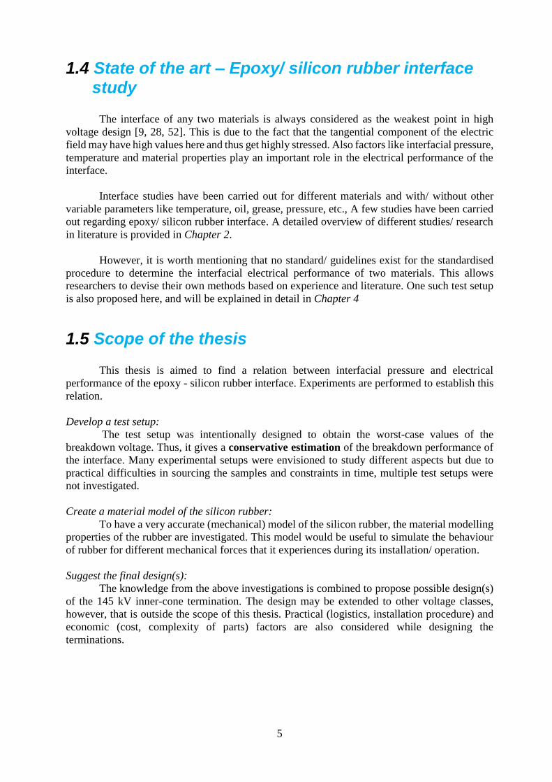
Fig. 1.4: Outline of thesis
•Motivation, State-of-the-art
•Scope, Research goalsIntroduction
•Solid/ solid interface study
•Epoxy/ silicon rubber interface studyLiterature study
•Drawbacks of linear modelling techniques,-Hyperelastic material model of currently used silicon rubber
Hyperelastic material modelling of silicon rubber
•Comparitive study of possible test setups
•Proposed test setup - advantages and limitationsDesign of test setup for
interface testing
•Procedure of testing
•Test results and inferencesExperimental study of epoxy/
silicon rubber interface
•CIGRE JWG recommendations
•Proposed designs 'A' and 'B'Design of inner-cone GIS
termination
•Conclusions
•Answers to research goalsConclusions and future scope

8

9
2. Literature study
This chapter provides a summary of various literature regarding solid/ solid interfaces
and more particularly about epoxy/ silicon rubber interface. The chapter is divided into different
sections and sub-sections based on the topic of research and its results.
10
2.1 Solid | solid interface study
Several failure investigations [9, 40] from the past reiterate the fact that the interface is
the weakest point of HV cable and cable systems. The interest of many organisations worldwide
to learn about interfaces stemmed from the 1993 blackout in The Netherlands [40]. This has
propelled great amount of research to be done to investigate the performance of interfaces to
establish a relation between various electrical and non-electrical parameters.
Solid/ solid interface study was done by various experts from different institutes around
the globe. A summary of the work by each institute is given below.
2.1.1 CIGRE WG 15-10
The focus of this WG was to propose a list [48] of requirements for testing of material
interfaces. The recommendations of this WG are used a s a basis to develop several test setups
[5, 29, 40, 51] which are explained in the following sub-sections. The requirements enlisted by
the CIGRE 15-10 WG (1996) are:
• Testing cells should have a simple configuration that is easy to reproduce.
• Testing cells should have no metal electrode surfacing at the interface.
• Testing cells should allow various defects to be introduced.
• Testing cells should enable one to study mechanical pressure effects.
• Testing cells should enable one to study surface roughness effects.
• Testing cells should enable one to study the effect of silicone oil or other liquid
insulants.
2.1.2 Study at Hydro-Quebec Institute of Research (IREQ)- Canada
The works of Daniel Fournier and Laurent Lamarre serve as a the earliest and yet one of
the most relevant literature in interface electrical performance related study.
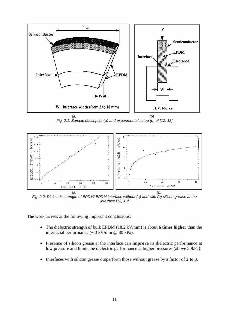
The works use a slightly-modified Baur breakdown cell as depicted in Fig.2.1. They
investigate the performance of EPDM | EPDM interface [13] and EPDM | XLPE interface [12].
The samples in both cases were cut from commercially available pieces.
Two pieces of the material under test are pressed against each other so as to induce
breakdown longitudinally along their interface. Two thin tungsten needle electrodes are
implanted at the interface, the distance between the electrodes is also varied with respect to
electric field. Weights are put on top of the sample to vary the pressure at the interface. The
effect of addition of silicon grease at the interface was also studied.
11
. (a) (b)
Fig. 2.1: Sample description(a) and experimental setup (b) of [12, 13]
(a) (b)
Fig. 2.2: Dielectric strength of EPDM/ EPDM interface without (a) and with (b) silicon grease at the interface [12, 13]
The work arrives at the following important conclusions:
• The dielectric strength of bulk EPDM (18.2 kV/mm) is about 6 times higher than the
interfacial performance (~ 3 kV/mm @ 80 kPa).
• Presence of silicon grease at the interface can improve its dielectric performance at
low pressure and limits the dielectric performance at higher pressures (above 50kPa).
• Interfaces with silicon grease outperform those without grease by a factor of 2 to 3.
12
2.1.3 Study at Norwegian University of Science and Technology
The works of Seyed Majid Hasheminezhad, Erling Ildstad, Arne Nysveen, Erme Kanter
and Dimitrios Panagiotopoulos provide a lot of insight into the study of solid/ solid interface
study and into the investigations for the relation of electrical breakdown strength with interface
pressure, surface roughness and temperature.
The main material interfaces studied in their works are XLPE | XLPE [14, 16, 46, 47]
XLPE | SiR [14, 16], SiR | SiR [14, 16]. The motivation for their work was with regard subsea
interconnectors. Thus, a lot of focus was given to compare the interface electric performance
during a dry and wet condition.
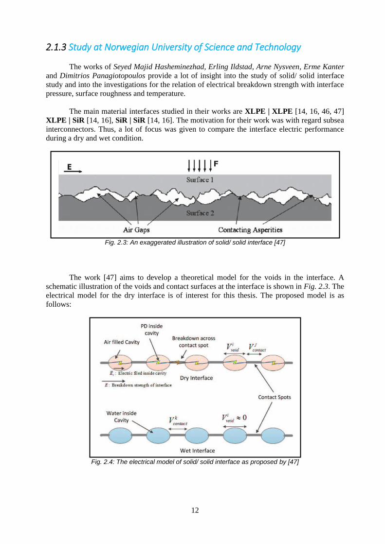
Fig. 2.3: An exaggerated illustration of solid/ solid interface [47]
The work [47] aims to develop a theoretical model for the voids in the interface. A
schematic illustration of the voids and contact surfaces at the interface is shown in Fig. 2.3. The
electrical model for the dry interface is of interest for this thesis. The proposed model is as
follows:
Fig. 2.4: The electrical model of solid/ solid interface as proposed by [47]
13
It was assumed that the breakdown voltage of the dry parts (Vdry) is composed of two
parameters (Vvoid) – voltage drops across the voids and (Vcontact) – voltage drops across the
contact spots.
(1)
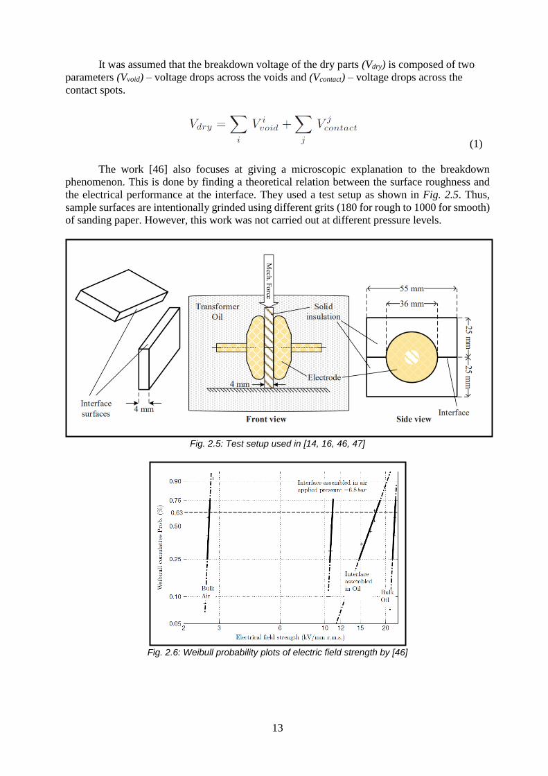
The work [46] also focuses at giving a microscopic explanation to the breakdown
phenomenon. This is done by finding a theoretical relation between the surface roughness and
the electrical performance at the interface. They used a test setup as shown in Fig. 2.5. Thus,
sample surfaces are intentionally grinded using different grits (180 for rough to 1000 for smooth)
of sanding paper. However, this work was not carried out at different pressure levels.
Fig. 2.5: Test setup used in [14, 16, 46, 47]
Fig. 2.6: Weibull probability plots of electric field strength by [46]
14
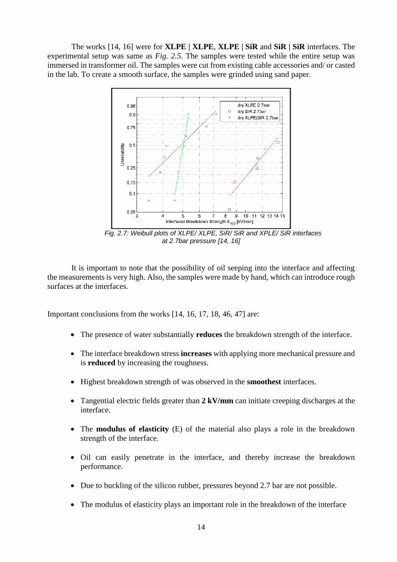
The works [14, 16] were for XLPE | XLPE, XLPE | SiR and SiR | SiR interfaces. The
experimental setup was same as Fig. 2.5. The samples were tested while the entire setup was
immersed in transformer oil. The samples were cut from existing cable accessories and/ or casted
in the lab. To create a smooth surface, the samples were grinded using sand paper.
Fig. 2.7: Weibull plots of XLPE/ XLPE, SiR/ SiR and XPLE/ SiR interfaces
at 2.7bar pressure [14, 16]
It is important to note that the possibility of oil seeping into the interface and affecting
the measurements is very high. Also, the samples were made by hand, which can introduce rough
surfaces at the interfaces.
Important conclusions from the works [14, 16, 17, 18, 46, 47] are:
• The presence of water substantially reduces the breakdown strength of the interface.
• The interface breakdown stress increases with applying more mechanical pressure and
is reduced by increasing the roughness.
• Highest breakdown strength of was observed in the smoothest interfaces.
• Tangential electric fields greater than 2 kV/mm can initiate creeping discharges at the
interface.
• The modulus of elasticity (E) of the material also plays a role in the breakdown
strength of the interface.
• Oil can easily penetrate in the interface, and thereby increase the breakdown
performance.
• Due to buckling of the silicon rubber, pressures beyond 2.7 bar are not possible.
• The modulus of elasticity plays an important role in the breakdown of the interface
15
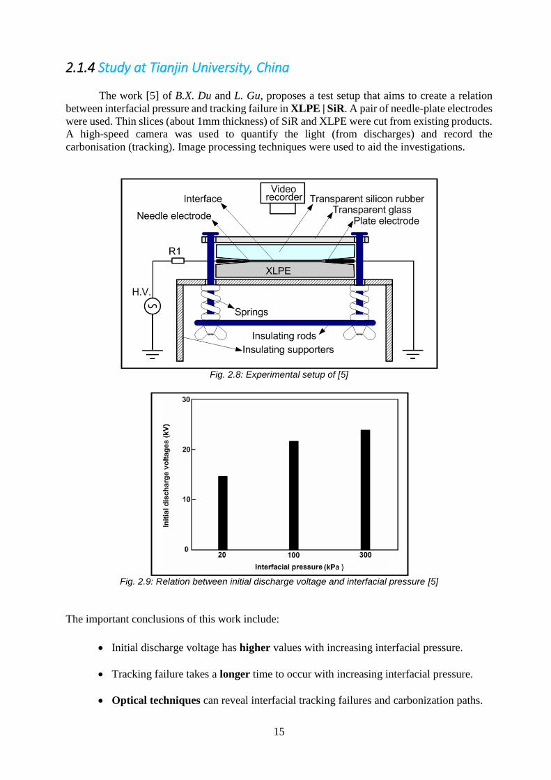
2.1.4 Study at Tianjin University, China
The work [5] of B.X. Du and L. Gu, proposes a test setup that aims to create a relation
between interfacial pressure and tracking failure in XLPE | SiR. A pair of needle-plate electrodes
were used. Thin slices (about 1mm thickness) of SiR and XLPE were cut from existing products.
A high-speed camera was used to quantify the light (from discharges) and record the
carbonisation (tracking). Image processing techniques were used to aid the investigations.
Fig. 2.8: Experimental setup of [5]
Fig. 2.9: Relation between initial discharge voltage and interfacial pressure [5]
The important conclusions of this work include:
• Initial discharge voltage has higher values with increasing interfacial pressure.
• Tracking failure takes a longer time to occur with increasing interfacial pressure.
• Optical techniques can reveal interfacial tracking failures and carbonization paths.
16
2.1.5 Study at KEMA, Netherlands
The work of Robert Ross [40] is a discussion about the 1993 blackout in the Netherlands
which was attributed to a cascade of breakdowns in a series of 150 kV terminations. During the
investigations, it was found that the XLPE | SiR interface was the reason for the series of failures.
The work illustrates how it was concluded that interfacial problems caused the cascade of
breakdowns. Important findings of this investigation were as follows:
• Treeing patterns were observed on both XLPE and SiR. The imprints were negatives of
each other.
• Electrical treeing occurred over a period of days/ months.
• Treeing started at the interface without any direct connection to any of the electrodes.
• Large increase in discharge activity was observed during temperature change. Difference
in thermal expansion coefficients, can cause the cable (XLPE) and termination (SiR) parts
to shift/ move along each other.
• In addition to the recommendations of CIGRE WG 15-10 [48], the test cell must also
allow the study of shear effects (motion and rubbing).
• Recommendation: Further investigations to understand the cause of interface problems,
introduction of dedicated PD monitoring methods.
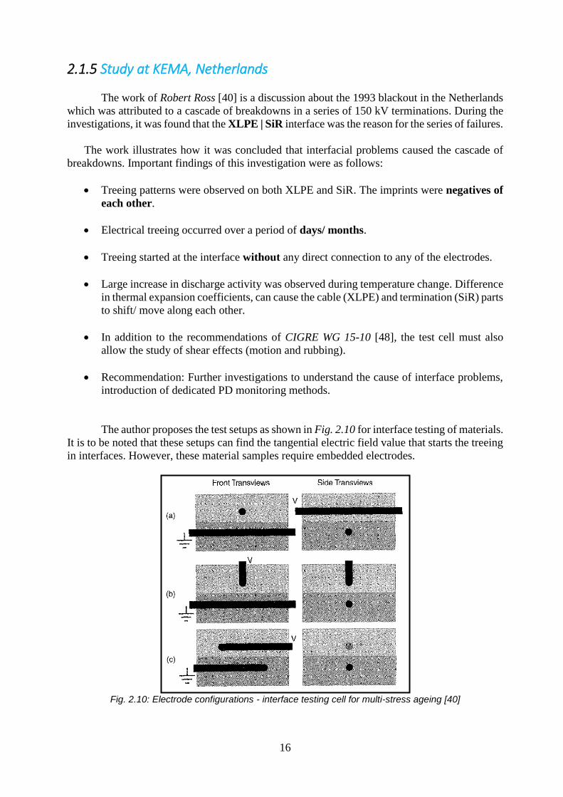
The author proposes the test setups as shown in Fig. 2.10 for interface testing of materials.
It is to be noted that these setups can find the tangential electric field value that starts the treeing
in interfaces. However, these material samples require embedded electrodes.
Fig. 2.10: Electrode configurations - interface testing cell for multi-stress ageing [40]
17
2.2 Epoxy/ SiR interface study
The interest of this thesis is to study the Epoxy | SiR interface, as this would be required
to verify the design of the new inner-cone GIS termination. Some studies have been carried out
by different institutes, which is elaborated in this section.
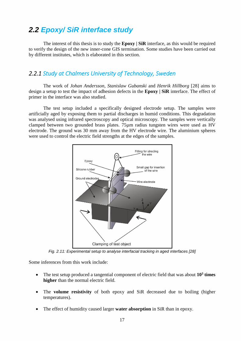
2.2.1 Study at Chalmers University of Technology, Sweden
The work of Johan Andersson, Stanislaw Gubanski and Henrik Hillborg [28] aims to
design a setup to test the impact of adhesion defects in the Epoxy | SiR interface. The effect of
primer in the interface was also studied.
The test setup included a specifically designed electrode setup. The samples were
artificially aged by exposing them to partial discharges in humid conditions. This degradation
was analysed using infrared spectroscopy and optical microscopy. The samples were vertically
clamped between two grounded brass plates. 75µm radius tungsten wires were used as HV
electrode. The ground was 30 mm away from the HV electrode wire. The aluminium spheres
were used to control the electric field strengths at the edges of the samples.
Fig. 2.11: Experimental setup to analyse interfacial tracking in aged interfaces [28]
Some inferences from this work include:
• The test setup produced a tangential component of electric field that was about 103 times
higher than the normal electric field.
• The volume resistivity of both epoxy and SiR decreased due to boiling (higher
temperatures).
• The effect of humidity caused larger water absorption in SiR than in epoxy.

18
• Due to PD, there were cracks observed on the surface of the aged samples.
• The degradation of epoxy is due to hydrolysis reactions
Although the research did not lead to any specific conclusions, it is specified here to give
a feeling of the different test setups and research works in this area.
2.2.2 Study at ABB Corporate Research, Sweden
The works of Cecilia Forssen, Anna Christerson and Daniel Borg proposes a novel test
setup for testing the effect of mechanical pressure and surface smoothness on the interfacial
electrical performance of the Epoxy | SiR interface. The work [7] gives the results of AC
breakdown testing while [8] provides an insight into the performance of the same test setup to
lightning impulse (LI) breakdown testing.
Fig. 2.12: Test setup of [7, 8]
The test setup consists of a conical rubber plug that is fitted into an epoxy disc. This disc
is then pressed between two electrodes. The test cell is compressed, and the pressure is controlled
through a plunger and spring assembly. There is a pressure sensor in the bottom electrode. The
whole test setup was cast in insulating gel to avoid flashover. The difference in breakdown
performance for rough and smooth interfaces was studied.
Some noticeable drawbacks of this test setup are as follows:
• the electric field at the epoxy/ SiR interface is non-uniform.
• the test setup and samples are complicated to reproduce
• the electrically active part of this test setup is only 10mm long.
• The test setup is cast in insulating gel / transformer oil, thus, there could be
influence of the gel on the results of the testing
19
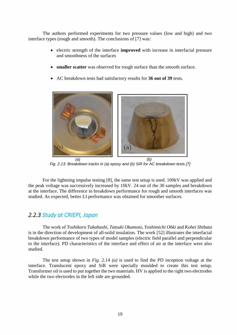
The authors performed experiments for two pressure values (low and high) and two
interface types (rough and smooth). The conclusions of [7] was:
• electric strength of the interface improved with increase in interfacial pressure
and smoothness of the surfaces
• smaller scatter was observed for rough surface than the smooth surface.
• AC breakdown tests had satisfactory results for 36 out of 39 tests.
(a) (b)
Fig. 2.13: Breakdown tracks in (a) epoxy and (b) SiR for AC breakdown tests [7]
For the lightning impulse testing [8], the same test setup is used. 100kV was applied and
the peak voltage was successively increased by 10kV. 24 out of the 30 samples and breakdown
at the interface. The difference in breakdown performance for rough and smooth interfaces was
studied. As expected, better LI performance was obtained for smoother surfaces.
2.2.3 Study at CRIEPI, Japan
The work of Toshikoro Takahashi, Tatsuki Okamoto, Yoshimichi Ohki and Kohei Shibata
is in the direction of development of all-solid insulation. The work [52] illustrates the interfacial
breakdown performance of two types of model samples (electric field parallel and perpendicular
to the interface). PD characteristics of the interface and effect of air at the interface were also
studied.
The test setup shown in Fig. 2.14 (a) is used to find the PD inception voltage at the
interface. Translucent epoxy and SiR were specially moulded to create this test setup.
Transformer oil is used to put together the two materials. HV is applied to the right two electrodes
while the two electrodes in the left side are grounded.
20
(a) (b)
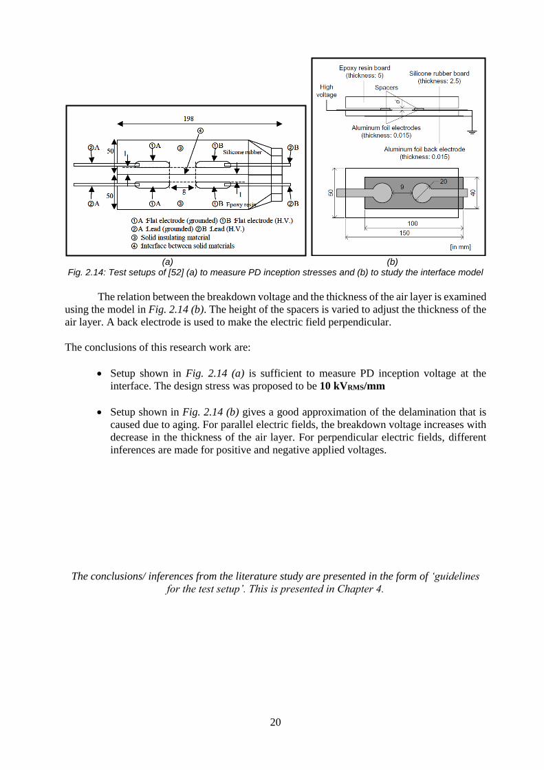
Fig. 2.14: Test setups of [52] (a) to measure PD inception stresses and (b) to study the interface model
The relation between the breakdown voltage and the thickness of the air layer is examined
using the model in Fig. 2.14 (b). The height of the spacers is varied to adjust the thickness of the
air layer. A back electrode is used to make the electric field perpendicular.
The conclusions of this research work are:
• Setup shown in Fig. 2.14 (a) is sufficient to measure PD inception voltage at the
interface. The design stress was proposed to be 10 kVRMS/mm
• Setup shown in Fig. 2.14 (b) gives a good approximation of the delamination that is
caused due to aging. For parallel electric fields, the breakdown voltage increases with
decrease in the thickness of the air layer. For perpendicular electric fields, different
inferences are made for positive and negative applied voltages.
The conclusions/ inferences from the literature study are presented in the form of ‘guidelines
for the test setup’. This is presented in Chapter 4.
21
3. Hyperelastic material modelling of silicon rubber
This chapter provides a detailed explanation about the need for such a material modelling
technique. It provides a detailed study of different modelling techniques (including linear elastic
modelling). It then explains about the different types of hyperelastic models and the model that
is chosen for the type of silicon rubber used in the GIS cable termination.

22
3.1 Stress – strain curves
Every engineering material is subject to external forces. When a solid object is deformed,
an internal reactive force tends to resist the deformation. This force is called stress. The measure
of deformation is called strain.
Every material is represented by a graphic figure known as the ‘stress-strain curve’. These
curves give a good understanding of the type of material and its behaviour to various types of
mechanical forces [15].
Fig. 3.1: Stress – strain curve of mild steel [54]
The stress-strain plots of materials are used as an important tool to classify their use for
different applications. The structural loadability of materials is found from this curve. The curve
also gives an understanding of properties like stiff/ elastic, hard/ soft, strong/ weak, brittle/ tough.
This thesis focusses on silicon rubber, as it would be the primary material of the inner-
cone termination. So, the mechanical tests on rubber will be explained here. Several tests
are performed to plot the stress strain curves. Each test helps to understand properties and
(possible) applications of the material.
Fig. 3.2: Types of stress-strain curves of different material types [54]

23
3.2 Need for hyperelastic material modelling
Rubber is a unique material by being very soft, exhibits very large strains, has a very
nonlinear stress-strain relation, has a low elastic modulus and is highly elastic [2, 30]. This allows
rubber are used for a variety of purposes from vehicle tyres, seals, hoses and so on.
Fig. 3.3: Types of stress strain curve of different material classifications [33, 54]
Linear elastic material follows the Hooke’s law which is given by the following relation
where, ‘σ’ is the stress, ‘ε’ is the strain and ‘E’ is the constant known as the Young’s modulus
or modulus of elasticity of the material.
σ = E. ε (2)
Elastomers like rubber are modelled as hyperelastic materials instead of linear elastic.
This is because the stress is determined by the current state of deformation and not the path or
history of deformation. This is shown in Fig. 3.4.
Fig. 3.4: Stress-strain curves of elastomers and linear elastic materials. [39]
24
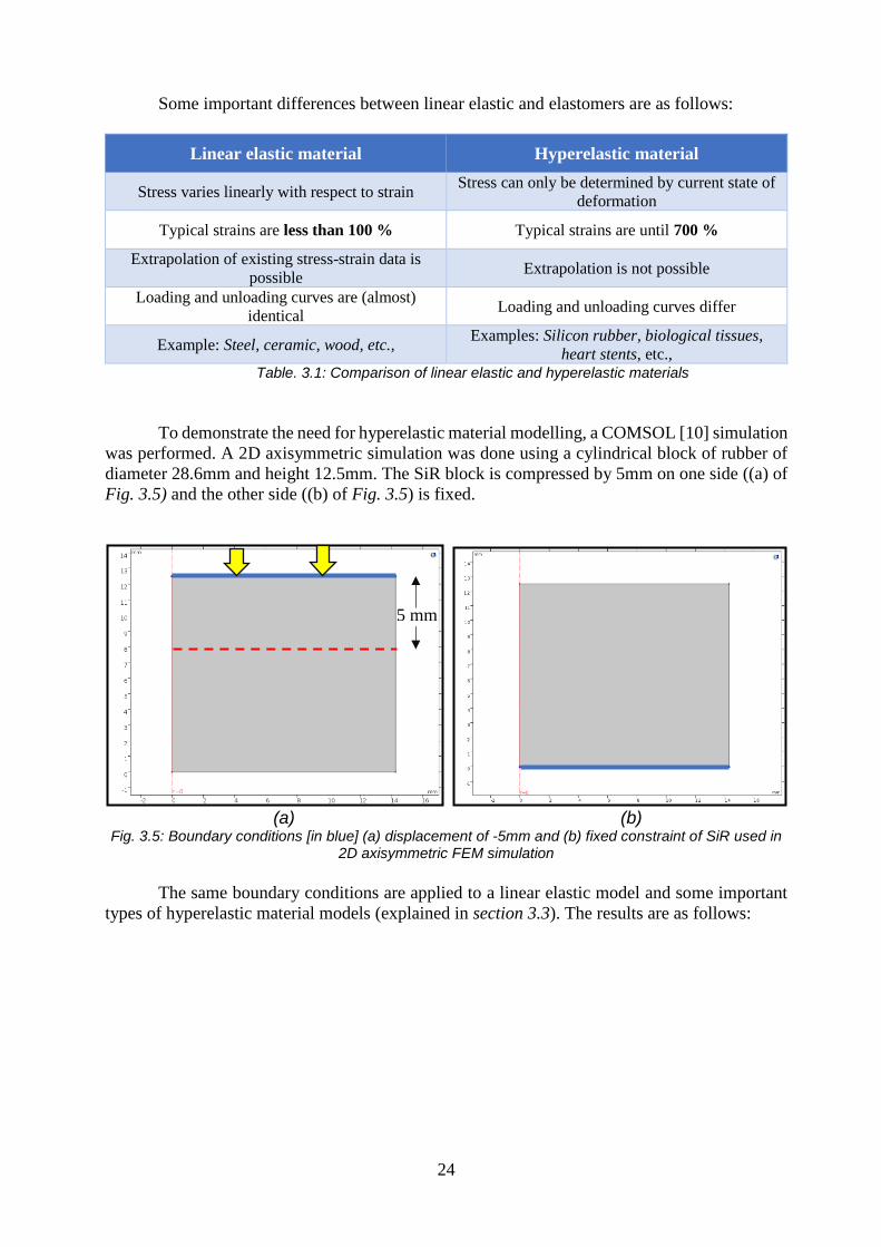
Some important differences between linear elastic and elastomers are as follows:
Linear elastic material Hyperelastic material
Stress varies linearly with respect to strain Stress can only be determined by current state of
deformation
Typical strains are less than 100 % Typical strains are until 700 %
Extrapolation of existing stress-strain data is
possible Extrapolation is not possible
Loading and unloading curves are (almost)
identical Loading and unloading curves differ
Example: Steel, ceramic, wood, etc., Examples: Silicon rubber, biological tissues,
heart stents, etc., Table. 3.1: Comparison of linear elastic and hyperelastic materials
To demonstrate the need for hyperelastic material modelling, a COMSOL [10] simulation
was performed. A 2D axisymmetric simulation was done using a cylindrical block of rubber of
diameter 28.6mm and height 12.5mm. The SiR block is compressed by 5mm on one side ((a) of
Fig. 3.5) and the other side ((b) of Fig. 3.5) is fixed.
(a) (b) Fig. 3.5: Boundary conditions [in blue] (a) displacement of -5mm and (b) fixed constraint of SiR used in
2D axisymmetric FEM simulation
The same boundary conditions are applied to a linear elastic model and some important
types of hyperelastic material models (explained in section 3.3). The results are as follows:
5 mm
25
Fig. 3.6 (a): Plot of von Mises stress (in MPa) for Linear Elastic model
Fig. 3.6 (b): Plot of von Mises stress (in MPa) for Mooney-Rivlin 2 parameter model
26
Fig. 3.6 (c): Plot of von Mises stress (in MPa) for Mooney-Rivlin 5 parameter model
Fig. 3.6 (d): Plot of von Mises stress (in MPa) for Arruda Boyce model
27
Fig. 3.6 (e): Plot of von Mises stress (in MPa) for Neo-Hookean model
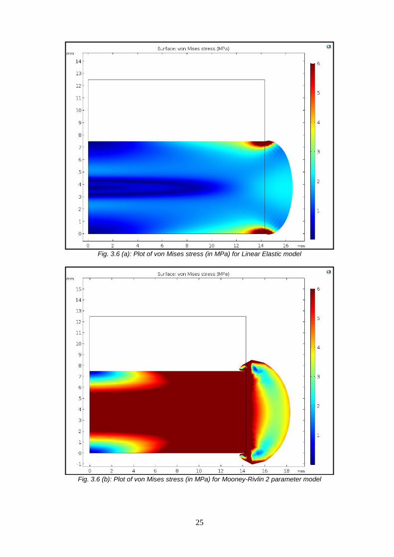
The various plots of the von Mises stress show, how the cylindrical block of silicon rubber
would behave when modelled using linear elastic method (Fig. 3.6 (a)) and using different
hyperelastic modelling techniques (Fig. 3.6 (b)- Fig. 3.6 (e)). It must be noted that almost all the
hyperelastic models exhibit a similar behaviour in terms of the deformation of rubber. It is also
important to note the difference in internal stresses between each type of modelling.
Another important feature that must be noted is during the bulging of rubber in
Fig. 3.6 (c), the high magnitude of forces/ stresses in the exterior (outer-most part) of the material
to control the shape of the rubber is visible – notice the high stress region at the edge of the
bulged SiR. This feature is also present in a lesser extent in the other hyperelastic simulations.
This is clearly absent in linear elastic model (Fig. 3.6 (a)) simulation.
3.3 Types of hyperelastic material modelling
To understand the different types of hyperelastic models, it is necessary to understand
some properties of hyperelastic materials.
Strain (ε) is defined as the ratio of the change in length of material (l1 – l0) to the original
length (l0).
ε = 𝑙1−𝑙0
𝑙0 =
Δl
𝑙𝑜 (3)
28
Stretch ratio (λ) is defined as the ratio of the current length to the original length of the
material.
𝜆 = 𝑙1
𝑙0=
𝑙1−𝑙0+𝑙0
𝑙0= 𝜀 + 1 (4)
Similarly, the principal strains in the three axes are represented as λ1, λ2 and λ3. The
three directions (axis) also have stretch invariants known as I1, I2 and I3. For hyperelastic
materials, another important property is the strain energy density function (W). It is a function
that relates the strain energy density to the deformation gradient. The general form of strain
energy density function equations is:
𝑊 = ∑ 𝐶𝑖𝑗(𝐼1
𝑁
𝑖+𝑗=1− 3)𝑖 (𝐼2 − 3)𝑗 + ∑
1
𝐷𝑘 (𝐽 − 1)2𝑘
𝑁
𝑘=1 (5)
Where Cij and Dk are material constants that are determined by curve fitting/ tests on the
material. Eqn. 5 shows that the strain energy density is a polynomial function and depending
on its order, one or more curves (inflection points) may appear.
Different types of hyperelastic models are created and modelled depending on the strain
rate of the material (SiR). Each of the types have distinct strain energy density function. Some of
the most commonly used types of modelling are as follows:
• Mooney Rivlin (2 parameter, 3 parameter, 5 parameter and 9 parameter model)
• Arruda Boyce model
• Neo Hookean model
• Ogden model (1st, 2nd and 3rd order models)
• Yeoh model (1st, 2nd and 3rd order models)
• Gent model
• Blatz – Ko
• Response Function model
• Polynomial model (1st, 2nd and 3rd order models)
Each of the above-mentioned material models are used for different types of elastomers
and for different applications (elevated temperature, different strain rates, etc.,). Detailed
explanation of the different model types is avoided in view of the objective of this thesis
report.

29
3.4 Mechanical tests of SiR
To quantify the silicon rubber used as an electrical insulator for the proposed GIS cable
termination, the first step is to perform some mechanical tests, in order to accurately obtain the
stress – strain relationships. These tests were carried out in accordance with various NEN/ ISO
standards.
Fig. 3.7: Types of mechanical tests performed on rubber [31]
Two frequently used tests for rubber are tensile (uniaxial, planar or biaxial) and
compression (uniaxial). NEN ISO – 37 [42] is used for the tensile strength measurements while
NEN ISO – 815/ NEN ISO - 7743 [43, 50] is used for the compression tests [31]. Uniaxial tensile
strength measurements were made at room temperature and at elevated temperature of
80 °C. The higher temperature was chosen as 80 °C because the maximum operating temperature
of the cable conductor is 90 °C.
Fig. 3.8: (b): Dumbbell shape samples
Fig. 3.8 (a): Test setup for tensile strength measurements
30
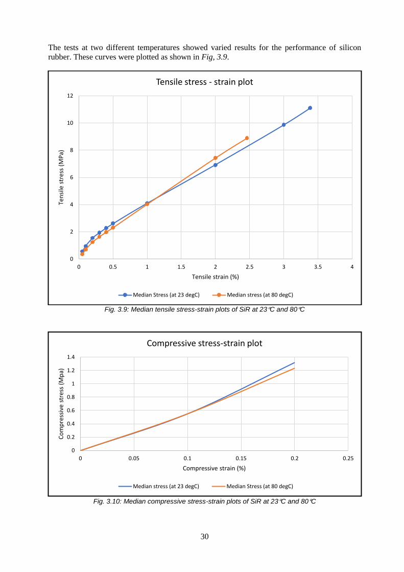
The tests at two different temperatures showed varied results for the performance of silicon
rubber. These curves were plotted as shown in Fig, 3.9.
Fig. 3.9: Median tensile stress-strain plots of SiR at 23°C and 80°C
Fig. 3.10: Median compressive stress-strain plots of SiR at 23°C and 80°C
0
2
4
6
8
10
12
0 0.5 1 1.5 2 2.5 3 3.5 4
Ten
sile
str
ess
(MP
a)
Tensile strain (%)
Tensile stress - strain plot
Median Stress (at 23 degC) Median stress (at 80 degC)
0
0.2
0.4
0.6
0.8
1
1.2
1.4
0 0.05 0.1 0.15 0.2 0.25
Co
mp
ress
ive
stre
ss (
Mp
a)
Compressive strain (%)
Compressive stress-strain plot
Median stress (at 23 degC) Median Stress (at 80 degC)
31
As per NEN ISO – 37 [42], the samples must be cut according to a predefined shape and
size. Then, the samples must be tested at a constant nominal velocity of 500 mm/ min. Five
samples were tested, and the median of the individual values were taken as the final values of the
material. Any test sample that breaks outside the narrow portion of the dumbbell is discarded and
a repeat measurement was done. It must be noted that the last point of each of the curves is the
point at which the sample broke.
Compressive tests were also performed on the silicon rubber at the two temperatures in
accordance to NEN ISO – 7743. Limited readings were taken due to practical limitations in the
test setup. The results of the tests are shown in Fig. 3.10.
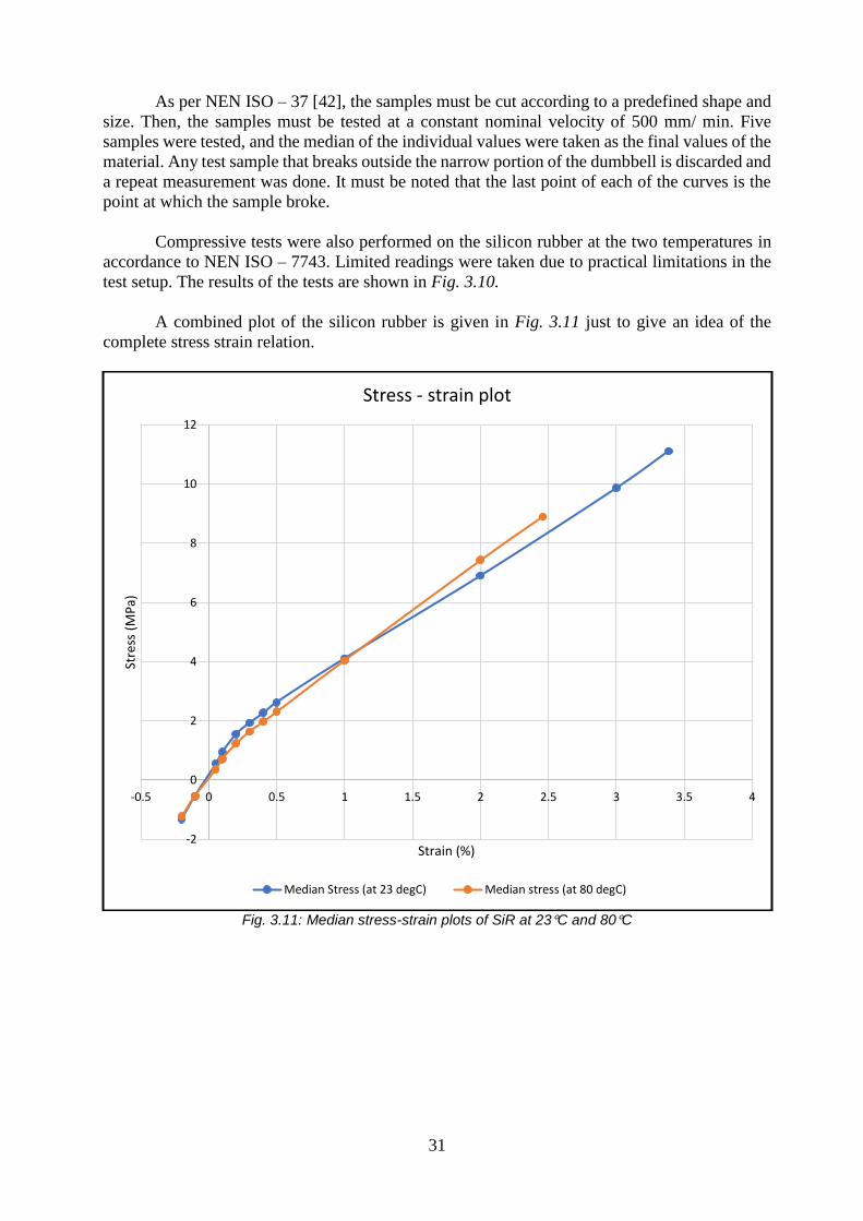
A combined plot of the silicon rubber is given in Fig. 3.11 just to give an idea of the
complete stress strain relation.
Fig. 3.11: Median stress-strain plots of SiR at 23°C and 80°C
-2
0
2
4
6
8
10
12
-0.5 0 0.5 1 1.5 2 2.5 3 3.5 4
Stre
ss (
MP
a)
Strain (%)
Stress - strain plot
Median Stress (at 23 degC) Median stress (at 80 degC)
32
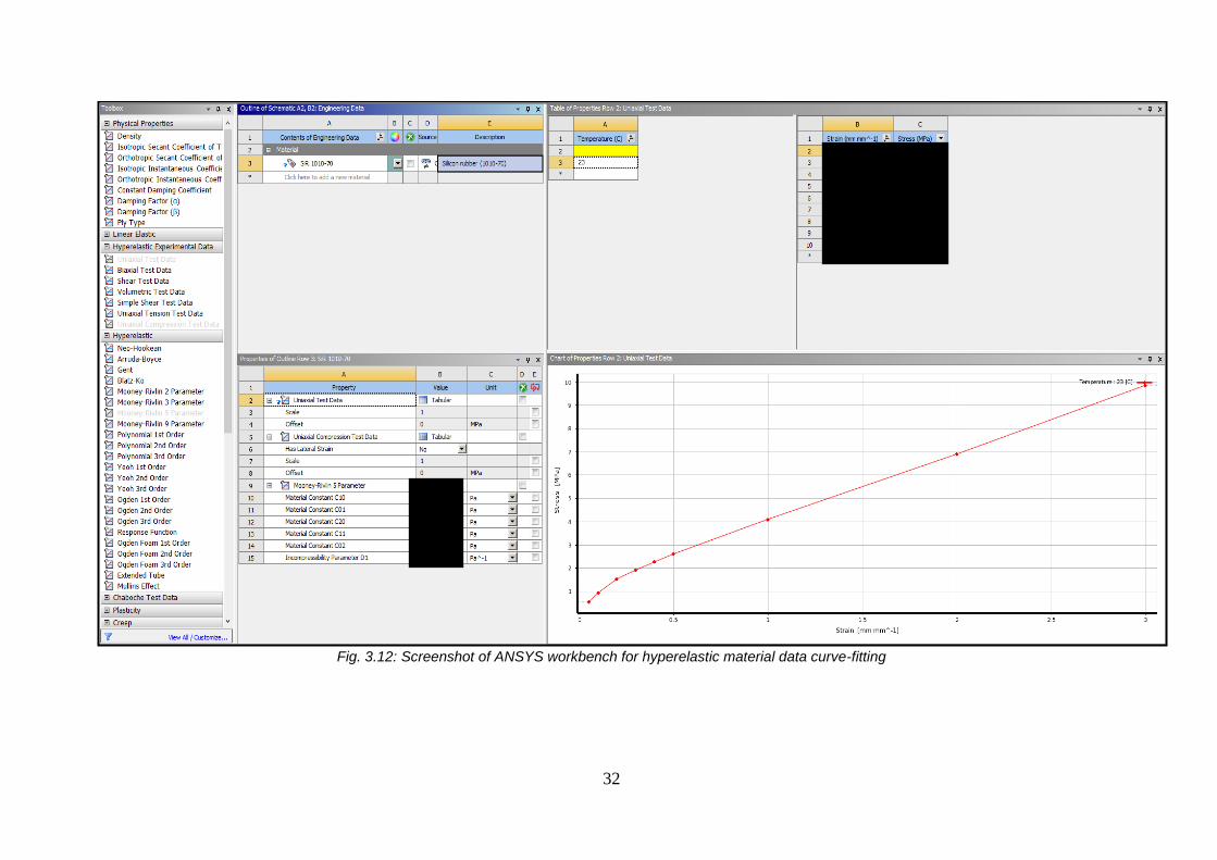
Fig. 3.12: Screenshot of ANSYS workbench for hyperelastic material data curve-fitting
33
3.5 Determining the type of material model
The stress-strain plots from Fig. 3.9 is used as an input to the ANSYS workbench [3].
The data is plotted and each method of hyperelastic material modelling is chosen and curve-
fitting is performed [11, 22, 32, 41, 51]. The software gives a curve-fit plot of the test data along
with the characteristic material constants (Eqn. 5). A screenshot of the ANSYS Workbench
window is shown in Fig. 3.12.
Each type of material model is checked with the available test data. The results of the
curve fitting process provide the material constants of the best fitted model (refer Eqn. 5). The
results from ANSYS workbench are as follows:
Results: Mooney Rivlin 5 parameter model (at 23°C)
Material constant C10
Material constant C01
Material constant C20
Material constant C11
Material constant C02
Results: Mooney Rivlin 5 parameter model (at 80°C)
Material constant C10
Material constant C01
Material constant C20
Material constant C11
Material constant C02
34
For 23°C, it is found that the curve fitting algorithm of ANSYS recognizes
Mooney Rivlin 5 parameter model as the best curve fit. Thus, this model is chosen as the
Hyperelastic material model for the silicon rubber at 23°C.
For 80°C, it is found that the curve fitting algorithm of ANSYS recognizes
Mooney Rivlin 5 parameter model as the best curve fit. Thus, this model is chosen as the
Hyperelastic material model for the silicon rubber at 80°C.
3.6 Conclusions
Mooney Rivlin 5 parameter model is chosen as the Hyperelastic material model of the
silicon rubber that is being used for this thesis (for experimental testing and for the GIS cable
termination).
The results of the curve fitting provide the material constants which are the parameters of
the strain energy density equation (Eqn. 5). These parameters will become the input for the FEM
software. However, it must be noted that the properties of rubber vary with temperature.

35
4. Design of test setup for interfacial study
This chapter provides a detailed explanation about the process of designing the test setup
that is used for interfacial testing. It then explains about the samples and each component of the
test setup. The chapter ends with a summary of the newly designed test setup.
36
4.1 Learning outcomes from literature study
A large variety of test setups are proposed by different authors in their respective works
for interfacial study. These setups were analysed in detail along with the CIGRE 15-10 [29]
recommendations. The drawbacks of each test setup were analysed in detail and some important
requirements for the test setup (for this thesis) were drafted. They are as ranked in descending
order of their importance, as follows:
1. Setup must withstand about 40 - 45 kV AC voltage without flashover.
This numerical value was estimated from literature study of similar interfaces.
2. Setup must withstand Lightning Impulse (LI) voltages up to 2-3 times the AC
breakdown value.
3. Setup must be able to mechanically withstand about 3 - 4 bar of interfacial pressure.
4. Setup must not be immersed in oil/ gel.
5. Setup must have no metal electrode at the interface [29].
6. Setup must have a simple configuration.
7. Setup must be modular i.e. easy to replace and upscale/ downscale if necessary.
8. Setup must not allow any misalignment of samples.
9. Samples should be easily producible.
10. Setup should be mechanically robust.
11. Setup should allow various surface defects to be introduced.
12. Setup should allow the study mechanical pressure effects.
13. Setup should enable one to study the effect of silicone oil or other liquid insulants.
These requirements were used as a basis to design the test setup. Different configurations
were analysed in detail. The test setup used in this thesis is explained in the next sections and
the reasons behind each feature/ parameter is also explained in detail.

37
4.2 Test setup – draft designs
A few draft designs were simulated using COMSOL Multiphysics, to understand the
electric field distribution and estimate the voltage levels needed. Some of the models are
mentioned here.
4.2.1 Draft setup #1: SiR- Epoxy
This setup involved thin layers of silicon rubber and epoxy being placed on top of each
other as shown in Fig. 4.1. Two circular electrodes are used for the HV and ground terminals
respectively. The electrodes are present on opposite sides. Non-metallic blocks are used as
weights to apply interfacial pressure. The FEM simulation of this setup was done at 1 kV of
applied voltage.
Fig. 4.1: Draft setup #1 - components
This setup has the following advantages:
• It had a tangential and normal component of electric field which is similar to the
actual interface in a GIS termination.
• The application of weights (interfacial pressure) is relatively simple as different
weights could be used to simulate different interfacial pressures.
epoxy
silicon rubber HV electrode
ground electrode (hidden from this view)
38
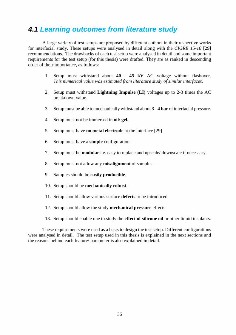
Fig. 4.2: Draft setup #1 – Tangential electric field at the interface
This setup has the following disadvantages:
• The tangential component of electric field is very small (0.05 kV/mm for
1 kV of applied voltage). This would mean that very large voltages should be
applied to observe interfacial breakdown.
• The contact area of the epoxy and silicon rubber is large – thus the
manufacturing of multiple samples for such a test setup would be cumbersome.
• The contact area of the epoxy and silicon rubber is large – thus large weights
would be necessary to create interfacial pressure of a few bar.
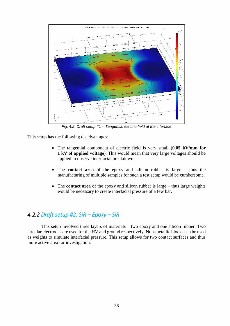
4.2.2 Draft setup #2: SiR – Epoxy – SiR
This setup involved three layers of materials – two epoxy and one silicon rubber. Two
circular electrodes are used for the HV and ground respectively. Non-metallic blocks can be used
as weights to simulate interfacial pressure. This setup allows for two contact surfaces and thus
more active area for investigation.
39
Fig. 4.3: Draft setup #2 - components
This setup has the following advantages:
• It has a tangential and normal component of electric field which is similar to the
actual interface in a GIS termination.
• The application of weights (interfacial pressure) is relatively simple as different
weights could be used to simulate different interfacial pressures.
• Two active surfaces meant that more investigation could be carried out into the
performance of the interface.
Fig. 4.4 (a): upper interface
HV electrode
ground electrode
epoxy
ground electrode
epoxy
ground electrode
silicon rubber
ground electrode
40
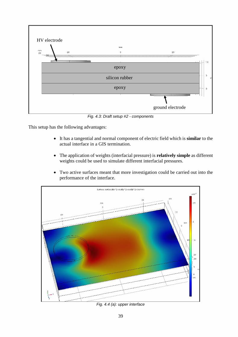
(b) lower interface
Fig. 4.4: Draft setup #2 – Tangential electric field at the interface
This setup has the following disadvantages:
• The tangential component of electric field is very small (0.025 kV/mm for
1 kV of applied voltage). This would mean that extremely large voltages should
be applied to observe interfacial breakdown.
• The contact area of the epoxy and silicon rubber is large – thus the
manufacturing of multiple samples for such a test setup would be cumbersome.
• The contact area of the epoxy and silicon rubber is large – thus large weights
would be necessary to create interfacial pressure of a few bar.
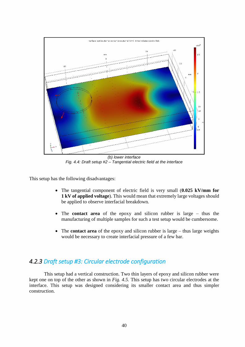
4.2.3 Draft setup #3: Circular electrode configuration
This setup had a vertical construction. Two thin layers of epoxy and silicon rubber were
kept one on top of the other as shown in Fig. 4.5. This setup has two circular electrodes at the
interface. This setup was designed considering its smaller contact area and thus simpler
construction.
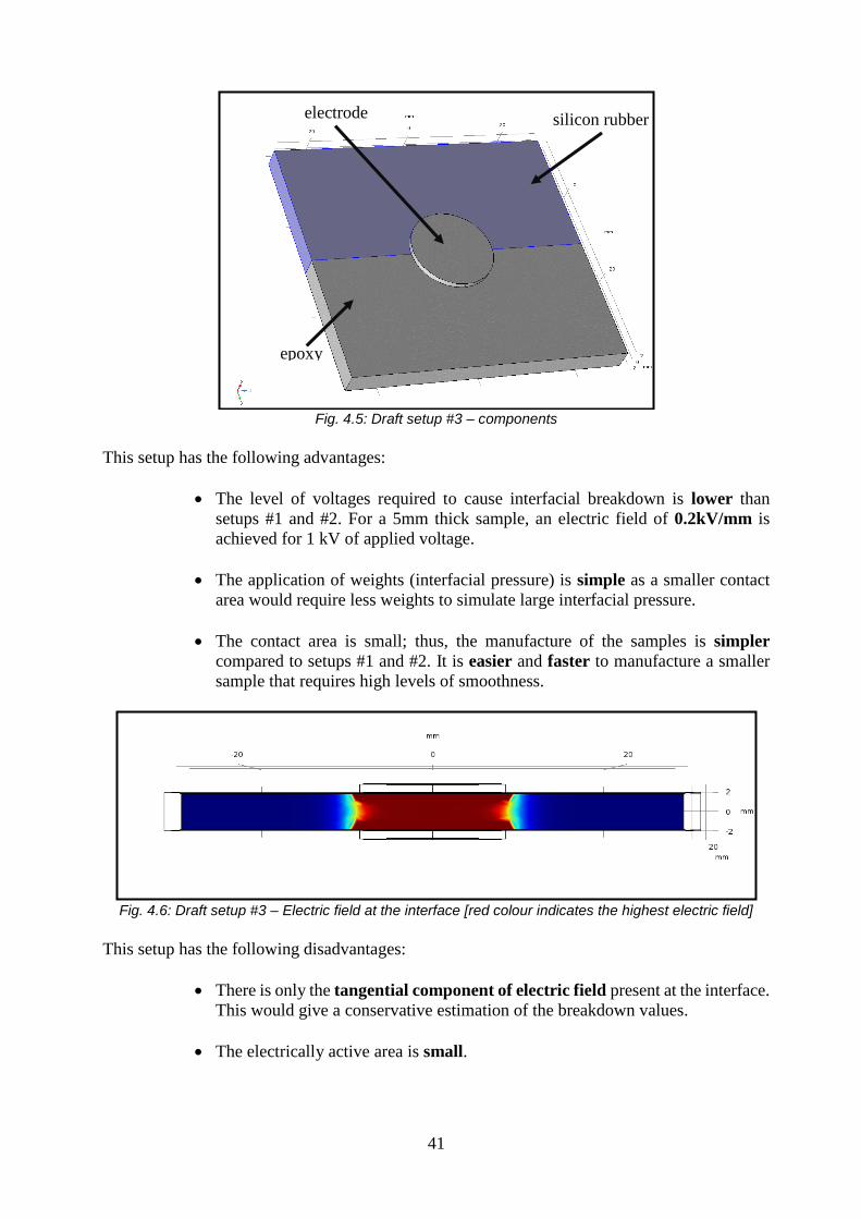
41
Fig. 4.5: Draft setup #3 – components
This setup has the following advantages:
• The level of voltages required to cause interfacial breakdown is lower than
setups #1 and #2. For a 5mm thick sample, an electric field of 0.2kV/mm is
achieved for 1 kV of applied voltage.
• The application of weights (interfacial pressure) is simple as a smaller contact
area would require less weights to simulate large interfacial pressure.
• The contact area is small; thus, the manufacture of the samples is simpler
compared to setups #1 and #2. It is easier and faster to manufacture a smaller
sample that requires high levels of smoothness.
Fig. 4.6: Draft setup #3 – Electric field at the interface [red colour indicates the highest electric field]
This setup has the following disadvantages:
• There is only the tangential component of electric field present at the interface.
This would give a conservative estimation of the breakdown values.
• The electrically active area is small.
epoxy
silicon rubber electrode
42
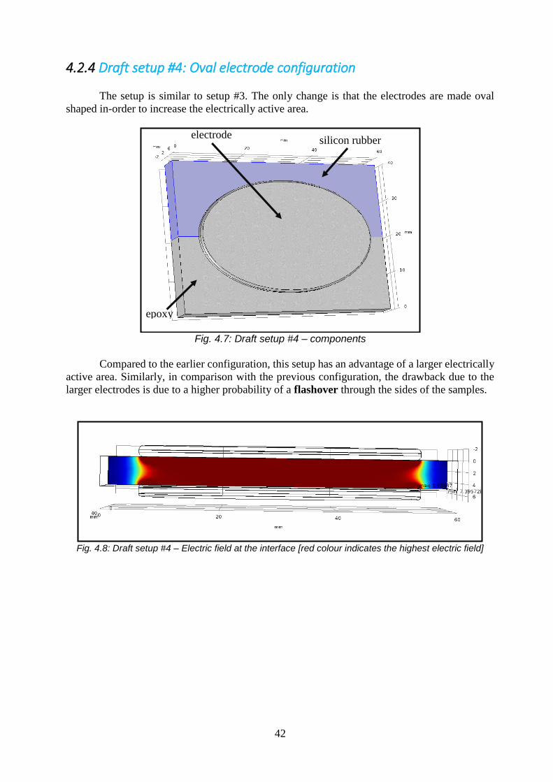
4.2.4 Draft setup #4: Oval electrode configuration
The setup is similar to setup #3. The only change is that the electrodes are made oval
shaped in-order to increase the electrically active area.
Fig. 4.7: Draft setup #4 – components
Compared to the earlier configuration, this setup has an advantage of a larger electrically
active area. Similarly, in comparison with the previous configuration, the drawback due to the
larger electrodes is due to a higher probability of a flashover through the sides of the samples.
Fig. 4.8: Draft setup #4 – Electric field at the interface [red colour indicates the highest electric field]
epoxy
silicon rubber electrode
43
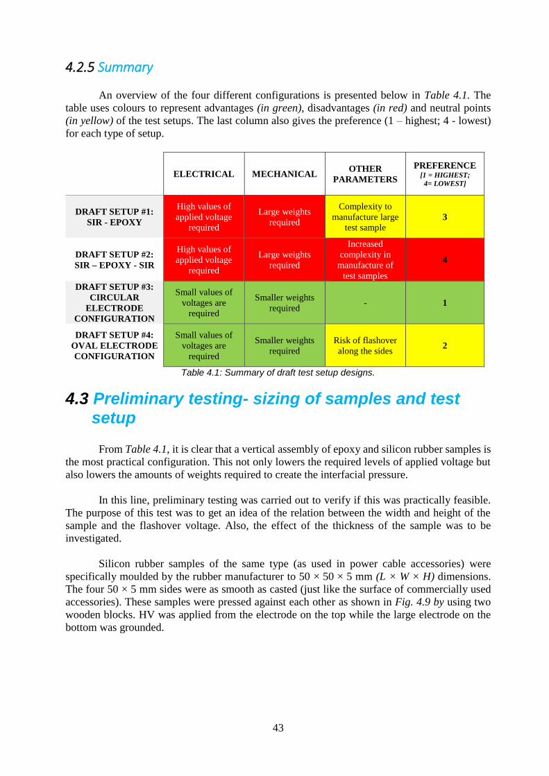
4.2.5 Summary
An overview of the four different configurations is presented below in Table 4.1. The
table uses colours to represent advantages (in green), disadvantages (in red) and neutral points
(in yellow) of the test setups. The last column also gives the preference (1 – highest; 4 - lowest)
for each type of setup.
ELECTRICAL MECHANICAL OTHER
PARAMETERS
PREFERENCE [1 = HIGHEST;
4= LOWEST]
DRAFT SETUP #1:
SIR - EPOXY
High values of
applied voltage
required
Large weights
required
Complexity to
manufacture large
test sample
3
DRAFT SETUP #2:
SIR – EPOXY - SIR
High values of
applied voltage
required
Large weights
required
Increased
complexity in
manufacture of
test samples
4
DRAFT SETUP #3:
CIRCULAR
ELECTRODE
CONFIGURATION
Small values of
voltages are
required
Smaller weights
required - 1
DRAFT SETUP #4:
OVAL ELECTRODE
CONFIGURATION
Small values of
voltages are
required
Smaller weights
required
Risk of flashover
along the sides 2
Table 4.1: Summary of draft test setup designs.
4.3 Preliminary testing- sizing of samples and test setup
From Table 4.1, it is clear that a vertical assembly of epoxy and silicon rubber samples is
the most practical configuration. This not only lowers the required levels of applied voltage but
also lowers the amounts of weights required to create the interfacial pressure.
In this line, preliminary testing was carried out to verify if this was practically feasible.
The purpose of this test was to get an idea of the relation between the width and height of the
sample and the flashover voltage. Also, the effect of the thickness of the sample was to be
investigated.
Silicon rubber samples of the same type (as used in power cable accessories) were
specifically moulded by the rubber manufacturer to 50 × 50 × 5 mm (L × W × H) dimensions.
The four 50 × 5 mm sides were as smooth as casted (just like the surface of commercially used
accessories). These samples were pressed against each other as shown in Fig. 4.9 by using two
wooden blocks. HV was applied from the electrode on the top while the large electrode on the
bottom was grounded.
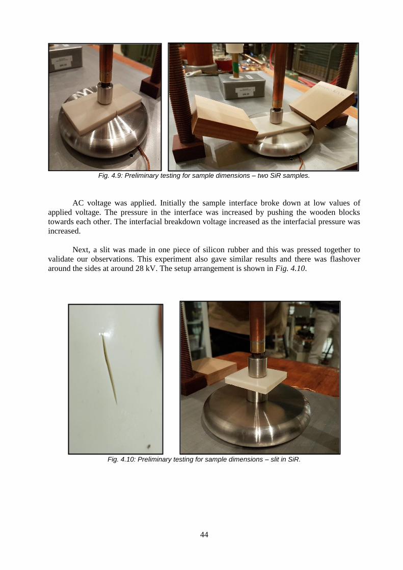
44
Fig. 4.9: Preliminary testing for sample dimensions – two SiR samples.
AC voltage was applied. Initially the sample interface broke down at low values of
applied voltage. The pressure in the interface was increased by pushing the wooden blocks
towards each other. The interfacial breakdown voltage increased as the interfacial pressure was
increased.
Next, a slit was made in one piece of silicon rubber and this was pressed together to
validate our observations. This experiment also gave similar results and there was flashover
around the sides at around 28 kV. The setup arrangement is shown in Fig. 4.10.
Fig. 4.10: Preliminary testing for sample dimensions – slit in SiR.
45
The following observations were made:
• It was noticed that the samples had flashover around 28 kV. This value is very low;
therefore, it was decided that wider samples were necessary.
• The rubber was beginning to bend at higher pressures. Thus, it would be better to
increase the thickness of rubber for better stability.
4.4 Design of test setup
Based on the requirements that were formulated in section 4.1 and the observations from
the preliminary testing (section 4.3) a test setup was designed such that it would incorporate all
the inferences/ conclusions. The reasoning and the final design is explained in detail in this
section.
4.4.1 Sample material
The samples were sourced directly from the supplier/ manufacturer of the epoxy and
silicon rubber respectively. This was done for the following reasons:
• The testing of actual materials would give a better estimation of the electric
breakdown performance.
• The manufacturer could smoothen/ polish the active surfaces (two 80 × 6 mm sides) to
be as smooth as casted. The samples would be as smooth as those used in commercial
cable accessories. This would eliminate ‘surface roughness’ problems that is common
in laboratory made samples.
• Time saving measure. The process of manufacturing samples in the laboratory was
found to be cumbersome and time consuming. Also, the risk of contamination of
samples is high due to non-industrial conditions.
4.4.2 Sample size
From the preliminary tests (section 4.3), it was clear that the samples must be wider than
50 mm. However, it must not be too wide as a wider sample (especially silicon rubber) risks
deformation/ buckling. Also, a large contact area would mean that larger weights are required to
create the required interfacial pressure.
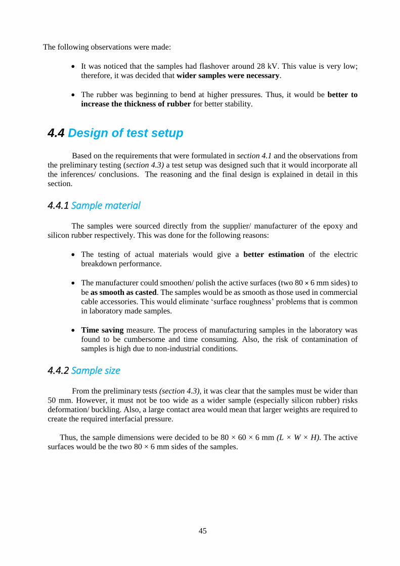
Thus, the sample dimensions were decided to be 80 × 60 × 6 mm (L × W × H). The active
surfaces would be the two 80 × 6 mm sides of the samples.
46
Fig. 4.11: Samples of silicon rubber (left) and epoxy (right).
4.4.3 Test holder
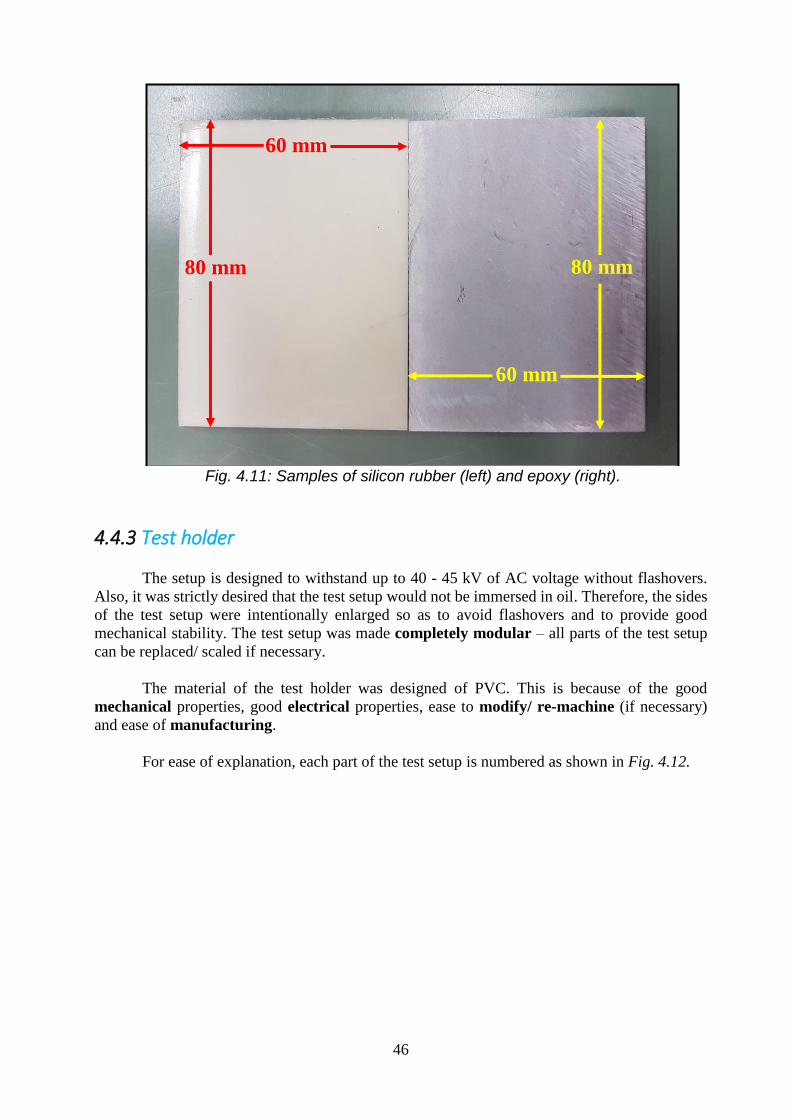
The setup is designed to withstand up to 40 - 45 kV of AC voltage without flashovers.
Also, it was strictly desired that the test setup would not be immersed in oil. Therefore, the sides
of the test setup were intentionally enlarged so as to avoid flashovers and to provide good
mechanical stability. The test setup was made completely modular – all parts of the test setup
can be replaced/ scaled if necessary.
The material of the test holder was designed of PVC. This is because of the good
mechanical properties, good electrical properties, ease to modify/ re-machine (if necessary)
and ease of manufacturing.
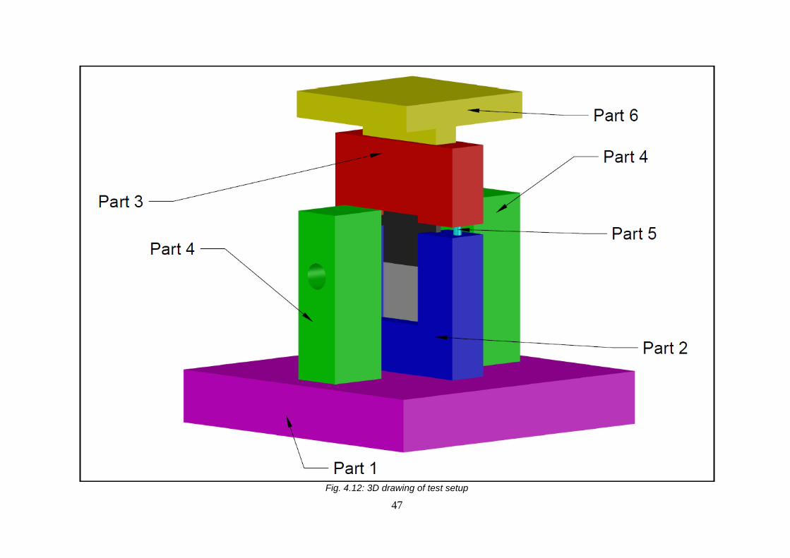
For ease of explanation, each part of the test setup is numbered as shown in Fig. 4.12.
80 mm 80 mm
60 mm
60 mm
47
Fig. 4.12: 3D drawing of test setup
48
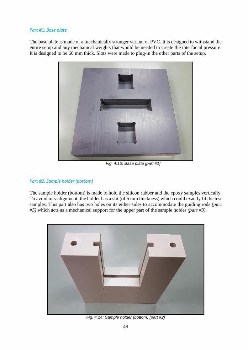
Part #1: Base plate
The base plate is made of a mechanically stronger variant of PVC. It is designed to withstand the
entire setup and any mechanical weights that would be needed to create the interfacial pressure.
It is designed to be 60 mm thick. Slots were made to plug-in the other parts of the setup.
Fig. 4.13: Base plate [part #1]
Part #2: Sample holder (bottom)
The sample holder (bottom) is made to hold the silicon rubber and the epoxy samples vertically.
To avoid mis-alignment, the holder has a slit (of 6 mm thickness) which could exactly fit the test
samples. This part also has two holes on its either sides to accommodate the guiding rods (part
#5) which acts as a mechanical support for the upper part of the sample holder (part #3).
Fig. 4.14: Sample holder (bottom) [part #2]
49
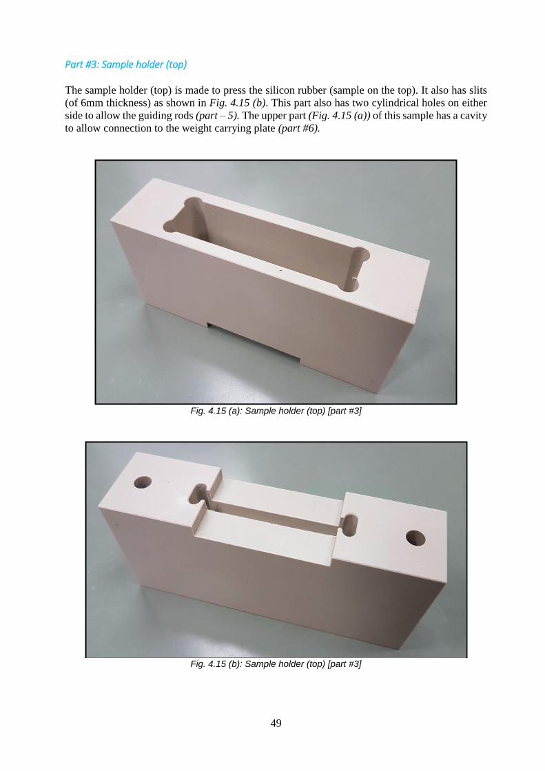
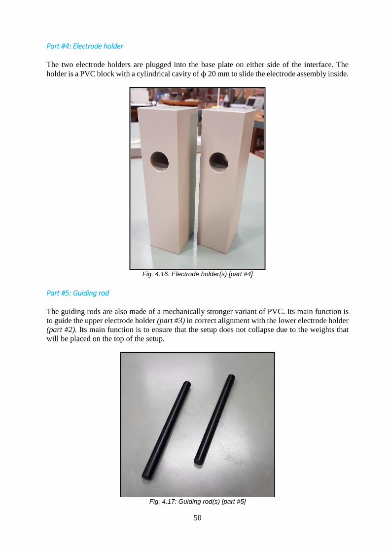
Part #3: Sample holder (top)
The sample holder (top) is made to press the silicon rubber (sample on the top). It also has slits
(of 6mm thickness) as shown in Fig. 4.15 (b). This part also has two cylindrical holes on either
side to allow the guiding rods (part – 5). The upper part (Fig. 4.15 (a)) of this sample has a cavity
to allow connection to the weight carrying plate (part #6).
Fig. 4.15 (a): Sample holder (top) [part #3]
Fig. 4.15 (b): Sample holder (top) [part #3]
50
Part #4: Electrode holder
The two electrode holders are plugged into the base plate on either side of the interface. The
holder is a PVC block with a cylindrical cavity of ϕ 20 mm to slide the electrode assembly inside.
Fig. 4.16: Electrode holder(s) [part #4]
Part #5: Guiding rod
The guiding rods are also made of a mechanically stronger variant of PVC. Its main function is
to guide the upper electrode holder (part #3) in correct alignment with the lower electrode holder
(part #2). Its main function is to ensure that the setup does not collapse due to the weights that
will be placed on the top of the setup.
Fig. 4.17: Guiding rod(s) [part #5]
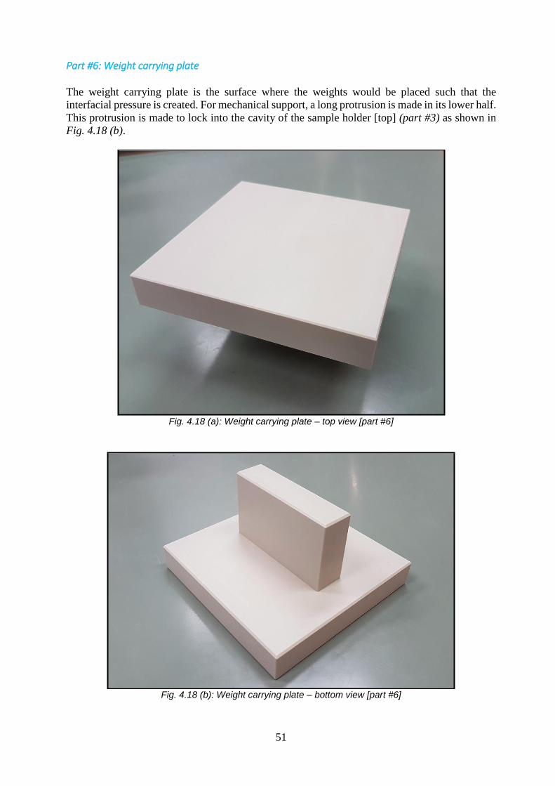
51
Part #6: Weight carrying plate
The weight carrying plate is the surface where the weights would be placed such that the
interfacial pressure is created. For mechanical support, a long protrusion is made in its lower half.
This protrusion is made to lock into the cavity of the sample holder [top] (part #3) as shown in
Fig. 4.18 (b).
Fig. 4.18 (a): Weight carrying plate – top view [part #6]
Fig. 4.18 (b): Weight carrying plate – bottom view [part #6]
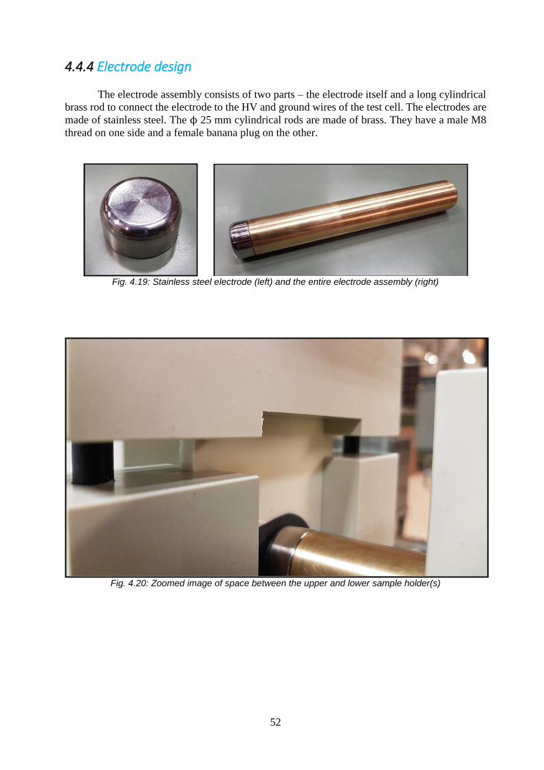
52
4.4.4 Electrode design
The electrode assembly consists of two parts – the electrode itself and a long cylindrical
brass rod to connect the electrode to the HV and ground wires of the test cell. The electrodes are
made of stainless steel. The ϕ 25 mm cylindrical rods are made of brass. They have a male M8
thread on one side and a female banana plug on the other.
Fig. 4.19: Stainless steel electrode (left) and the entire electrode assembly (right)
Fig. 4.20: Zoomed image of space between the upper and lower sample holder(s)
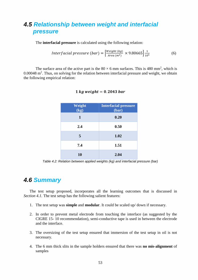
53
4.5 Relationship between weight and interfacial pressure
The interfacial pressure is calculated using the following relation:
𝐼𝑛𝑡𝑒𝑟𝑓𝑎𝑐𝑖𝑎𝑙 𝑝𝑟𝑒𝑠𝑠𝑢𝑟𝑒 (𝑏𝑎𝑟) = [𝑊𝑒𝑖𝑔ℎ𝑡 (𝑘𝑔)
𝐴𝑟𝑒𝑎 (𝑚2) × 9.80665]
1
105 (6)
The surface area of the active part is the 80 × 6 mm surfaces. This is 480 mm2, which is
0.00048 m2. Thus, on solving for the relation between interfacial pressure and weight, we obtain
the following empirical relation:
𝟏 𝒌𝒈 𝒘𝒆𝒊𝒈𝒉𝒕 = 𝟎. 𝟐𝟎𝟒𝟑 𝒃𝒂𝒓
Weight
(kg)
Interfacial pressure
(bar)
1 0.20
2.4 0.50
5 1.02
7.4 1.51
10 2.04
Table 4.2: Relation between applied weights (kg) and interfacial pressure (bar)
4.6 Summary
The test setup proposed, incorporates all the learning outcomes that is discussed in
Section 4.1. The test setup has the following salient features:
1. The test setup was simple and modular. It could be scaled up/ down if necessary.
2. In order to prevent metal electrode from touching the interface (as suggested by the
CIGRE 15- 10 recommendation), semi-conductive tape is used in between the electrode
and the interface.
3. The oversizing of the test setup ensured that immersion of the test setup in oil is not
necessary.
4. The 6 mm thick slits in the sample holders ensured that there was no mis-alignment of
samples
54
5. The electrode holders ensured that there was no mis-alignment in applying voltage to
the interface.
6. The guiding rods ensured that the setup would not topple (due to heavy weights). If the
rubber buckled, then the entire weight would be taken over by the guiding rods.
7. The setup was oversized intentionally to prevent flashovers and withstand larger weights.
8. 20 mm of length was allowed for the silicon rubber to compress (refer Fig. 4.20).
9. It was possible to study the effect of defects on the material and the effect of silicone oil
and other liquid insulants.
10. The electrode size could be increased/ decreased if necessary.
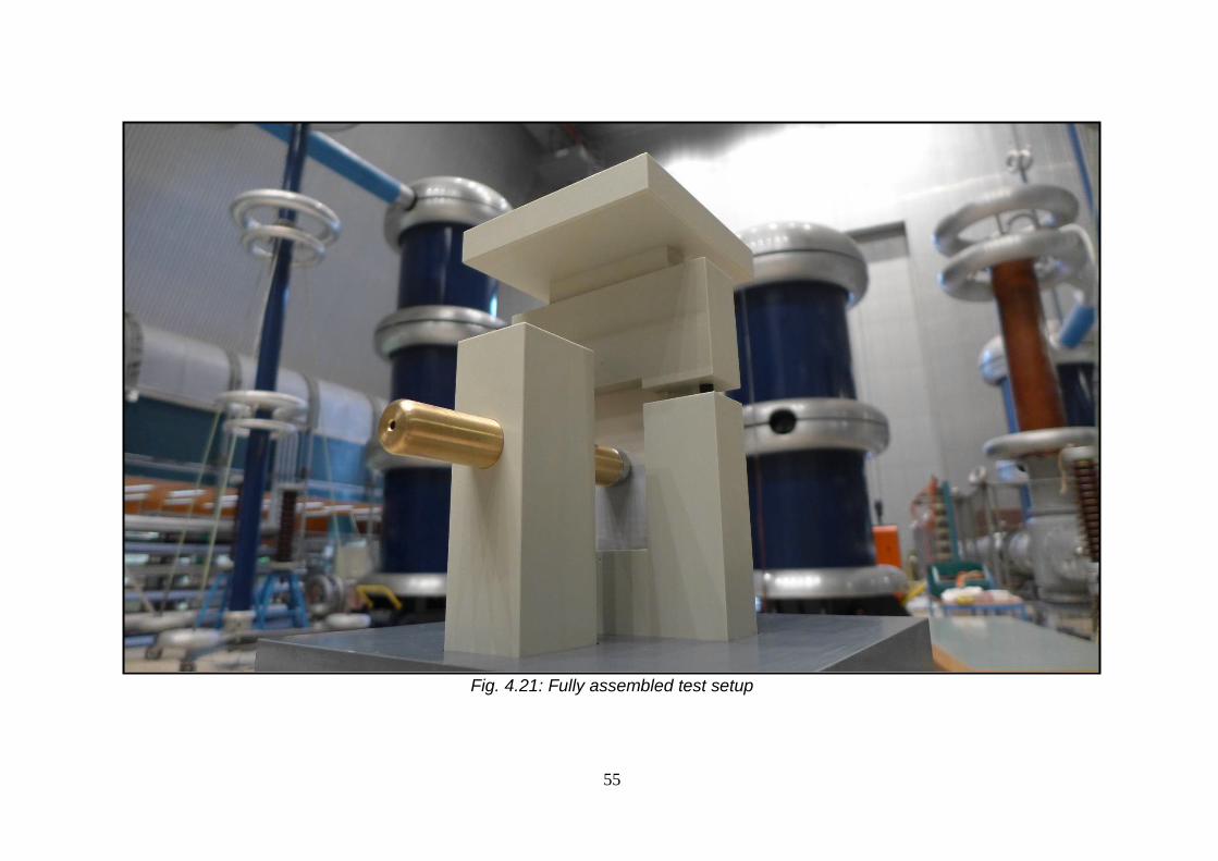
55
Fig. 4.21: Fully assembled test setup

56
57
5. Experimental study of epoxy/ silicon rubber interface
This chapter explains about the various tests (AC breakdown and lightning impulse tests)
that were performed on the epoxy/ silicon rubber interface. The test protocol for each test and
the corresponding results are provided. Pictures from the investigation and findings are also
included.
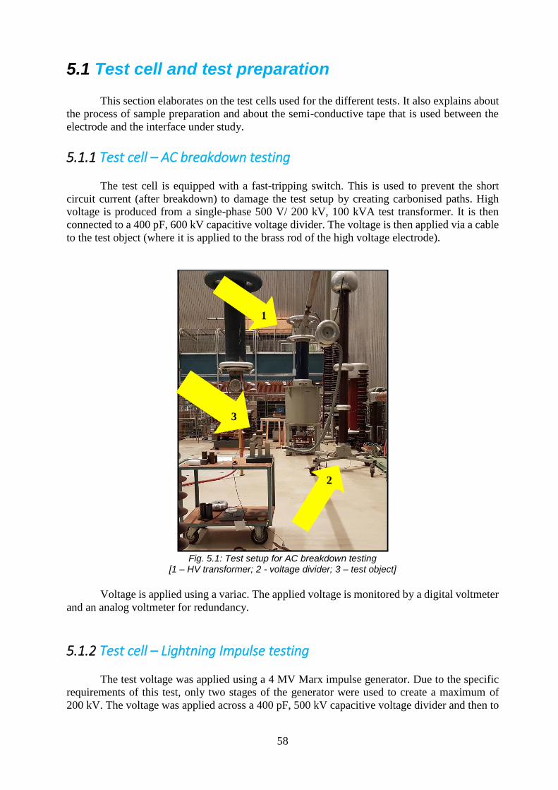
58
5.1 Test cell and test preparation
This section elaborates on the test cells used for the different tests. It also explains about
the process of sample preparation and about the semi-conductive tape that is used between the
electrode and the interface under study.
5.1.1 Test cell – AC breakdown testing
The test cell is equipped with a fast-tripping switch. This is used to prevent the short
circuit current (after breakdown) to damage the test setup by creating carbonised paths. High
voltage is produced from a single-phase 500 V/ 200 kV, 100 kVA test transformer. It is then
connected to a 400 pF, 600 kV capacitive voltage divider. The voltage is then applied via a cable
to the test object (where it is applied to the brass rod of the high voltage electrode).
Fig. 5.1: Test setup for AC breakdown testing
[1 – HV transformer; 2 - voltage divider; 3 – test object]
Voltage is applied using a variac. The applied voltage is monitored by a digital voltmeter
and an analog voltmeter for redundancy.
5.1.2 Test cell – Lightning Impulse testing
The test voltage was applied using a 4 MV Marx impulse generator. Due to the specific
requirements of this test, only two stages of the generator were used to create a maximum of
200 kV. The voltage was applied across a 400 pF, 500 kV capacitive voltage divider and then to
1
2
3
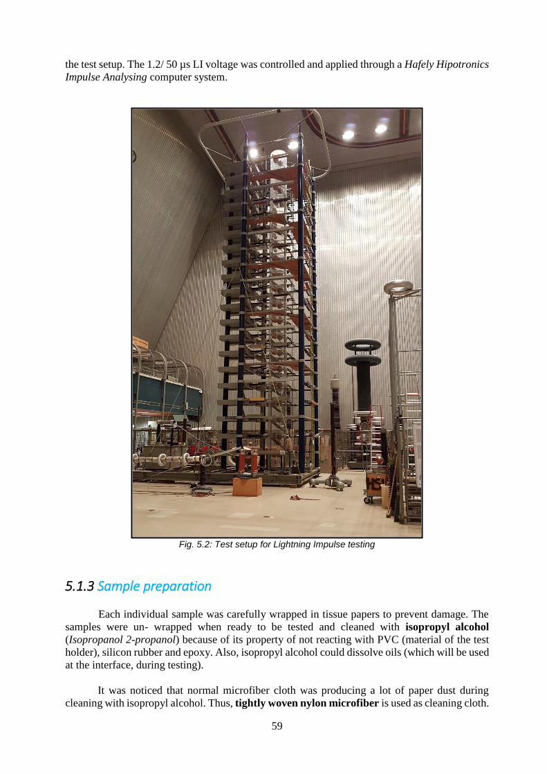
59
the test setup. The 1.2/ 50 µs LI voltage was controlled and applied through a Hafely Hipotronics
Impulse Analysing computer system.
Fig. 5.2: Test setup for Lightning Impulse testing
5.1.3 Sample preparation
Each individual sample was carefully wrapped in tissue papers to prevent damage. The
samples were un- wrapped when ready to be tested and cleaned with isopropyl alcohol
(Isopropanol 2-propanol) because of its property of not reacting with PVC (material of the test
holder), silicon rubber and epoxy. Also, isopropyl alcohol could dissolve oils (which will be used
at the interface, during testing).
It was noticed that normal microfiber cloth was producing a lot of paper dust during
cleaning with isopropyl alcohol. Thus, tightly woven nylon microfiber is used as cleaning cloth.

60
5.1.4 Semi-conductive tape
Fig. 5.3: Oval shaped hand-cut semi-conductive tapes
In-order to prevent the metal electrodes from making physical contact with the interface
under test [40, 48], it was decided to use semi-conductive tape at the interface. The tape is
30 mm wide and 1.5 mm thick. The tapes were cut by hand into oval shape. This also helped to
subside the electric field enhancement at the edges of the metal electrodes. Any sharp edges in
the tapes were manually rounded-off to prevent field enhancement.
5.2 AC Breakdown tests
The aim of this thesis is to deduce a relation between the interfacial pressure and the AC
breakdown voltage of the interface. This test is explained in detail in this section. It starts with
the test procedure and then shows the results.
5.2.1 Test procedure
The test cell is cleaned, and all unnecessary equipment is disconnected/ moved. Then,
the cell is checked for its safety systems by applying a small voltage and tripping the system.
This allows us to check if the power electronics based fast switch is working. Also, the
interlocking gates of the test cell are checked in this way.
The semi-conductive tape is cut by hand into oval pieces as shown in Fig. 5.3. Any sharp
corners in the tape are rounded off. The plastic cover on one side of the tape is removed just
before the testing.
The test setup is assembled by cleaning each of the parts with isopropyl alcohol and
drying them. The electrodes are also thoroughly cleaned. The parts are then plugged-into the
base plate and the entire test setup is assembled. The test setup was placed on a movable cart, to
enable the moving of the test setup for cleaning and other practical reasons.

61
The epoxy and silicon rubber samples are first checked for defects/ scratches in the
active region (80 × 6 mm sides). If no problems are found, they are cleaned using isopropyl
alcohol and allowed to dry.
The samples and the electrodes are assembled together. The oval semi-conductive tape is
stuck to the interface and then the electrode is pressed on the tape to allow good adhesion. The
specific weights are then kept on the weight carrying plate. It is ensured that the weights are kept
in the middle to prevent the setup from toppling.
The grounding stick is removed, and test cage is closed. Then, the voltage is applied at a
rate of 1kV/second. This rate of rise is within the short-time test requirements as stipulated by
ASTM standards [4]. Applied voltage is monitored on both the voltmeters.
After breakdown, the fast switch trips the circuit. Then, the variac is brought back to zero
and the breakdown voltage is recorded. The test cell is opened, and the grounding stick is then
put in place to ground the secondary of the HV transformer and the voltage divider.
The weights are removed and the top sample (silicon rubber) is removed to investigate
the breakdown area. If the breakdown originates at the triple point (at the edge of the semi-
conductive tape), the reading is discarded.
The breakdown paths are photographed. Then, the samples are marked with permanent
marker and safely stored in zip lock pouches. The test setup and the electrodes are then cleaned
with isopropyl alcohol and the next sample is prepared for investigation.
The entire process is shown as a flowchart in Fig. 5.4.
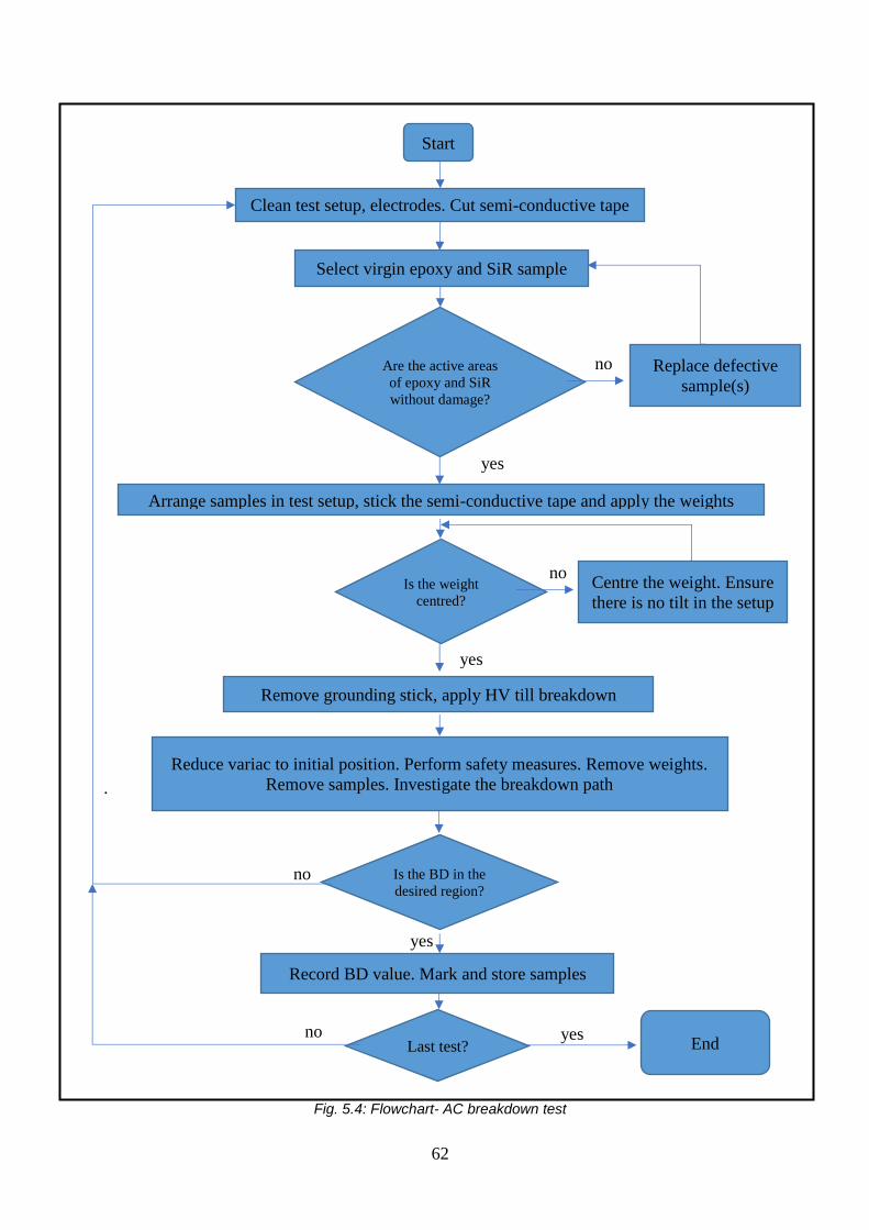
62
.
Fig. 5.4: Flowchart- AC breakdown test
Start
Clean test setup, electrodes. Cut semi-conductive tape
Are the active areas
of epoxy and SiR
without damage?
Arrange samples in test setup, stick the semi-conductive tape and apply the weights
Is the weight
centred?
yes
no Replace defective
sample(s)
Select virgin epoxy and SiR sample
yes
Remove grounding stick, apply HV till breakdown
Centre the weight. Ensure
there is no tilt in the setup
Reduce variac to initial position. Perform safety measures. Remove weights.
Remove samples. Investigate the breakdown path
Is the BD in the
desired region?
Record BD value. Mark and store samples
Last test? End
yes
no
yes no
no
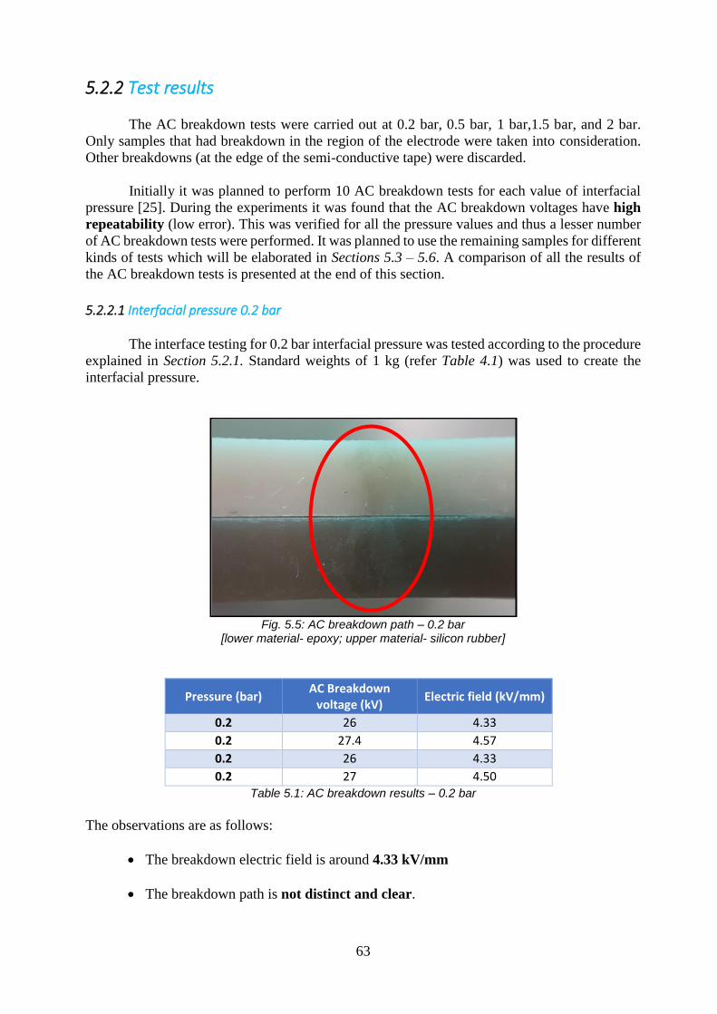
63
5.2.2 Test results
The AC breakdown tests were carried out at 0.2 bar, 0.5 bar, 1 bar,1.5 bar, and 2 bar.
Only samples that had breakdown in the region of the electrode were taken into consideration.
Other breakdowns (at the edge of the semi-conductive tape) were discarded.
Initially it was planned to perform 10 AC breakdown tests for each value of interfacial
pressure [25]. During the experiments it was found that the AC breakdown voltages have high
repeatability (low error). This was verified for all the pressure values and thus a lesser number
of AC breakdown tests were performed. It was planned to use the remaining samples for different
kinds of tests which will be elaborated in Sections 5.3 – 5.6. A comparison of all the results of
the AC breakdown tests is presented at the end of this section.
5.2.2.1 Interfacial pressure 0.2 bar
The interface testing for 0.2 bar interfacial pressure was tested according to the procedure
explained in Section 5.2.1. Standard weights of 1 kg (refer Table 4.1) was used to create the
interfacial pressure.
Fig. 5.5: AC breakdown path – 0.2 bar
[lower material- epoxy; upper material- silicon rubber]
Pressure (bar) AC Breakdown
voltage (kV) Electric field (kV/mm)
0.2 26 4.33
0.2 27.4 4.57
0.2 26 4.33
0.2 27 4.50 Table 5.1: AC breakdown results – 0.2 bar
The observations are as follows:
• The breakdown electric field is around 4.33 kV/mm
• The breakdown path is not distinct and clear.
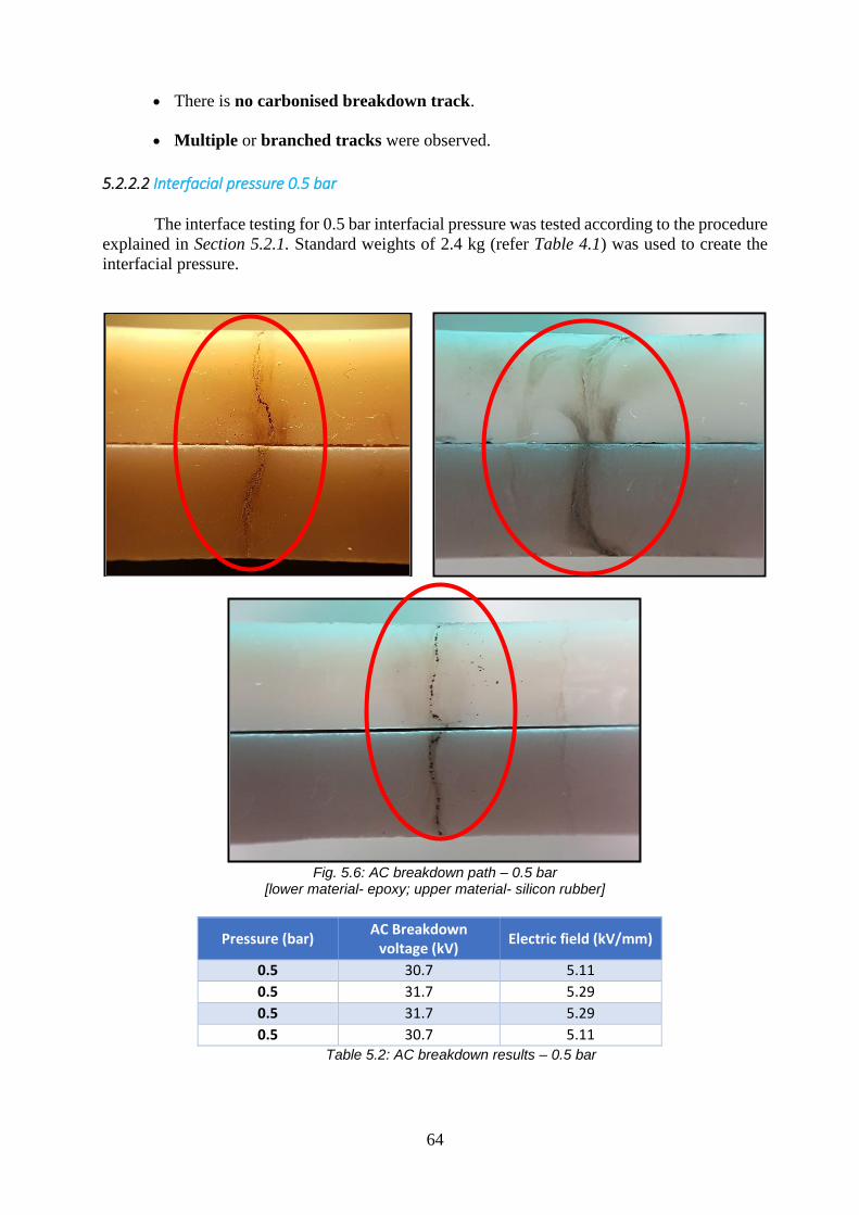
64
• There is no carbonised breakdown track.
• Multiple or branched tracks were observed.
5.2.2.2 Interfacial pressure 0.5 bar
The interface testing for 0.5 bar interfacial pressure was tested according to the procedure
explained in Section 5.2.1. Standard weights of 2.4 kg (refer Table 4.1) was used to create the
interfacial pressure.
Fig. 5.6: AC breakdown path – 0.5 bar
[lower material- epoxy; upper material- silicon rubber]
Pressure (bar) AC Breakdown
voltage (kV) Electric field (kV/mm)
0.5 30.7 5.11
0.5 31.7 5.29
0.5 31.7 5.29
0.5 30.7 5.11 Table 5.2: AC breakdown results – 0.5 bar
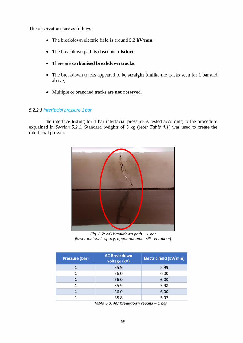
65
The observations are as follows:
• The breakdown electric field is around 5.2 kV/mm.
• The breakdown path is clear and distinct.
• There are carbonised breakdown tracks.
• The breakdown tracks appeared to be straight (unlike the tracks seen for 1 bar and
above).
• Multiple or branched tracks are not observed.
5.2.2.3 Interfacial pressure 1 bar
The interface testing for 1 bar interfacial pressure is tested according to the procedure
explained in Section 5.2.1. Standard weights of 5 kg (refer Table 4.1) was used to create the
interfacial pressure.
Fig. 5.7: AC breakdown path – 1 bar
[lower material- epoxy; upper material- silicon rubber]
Pressure (bar) AC Breakdown
voltage (kV) Electric field (kV/mm)
1 35.9 5.99
1 36.0 6.00
1 36.0 6.00
1 35.9 5.98
1 36.0 6.00
1 35.8 5.97 Table 5.3: AC breakdown results – 1 bar
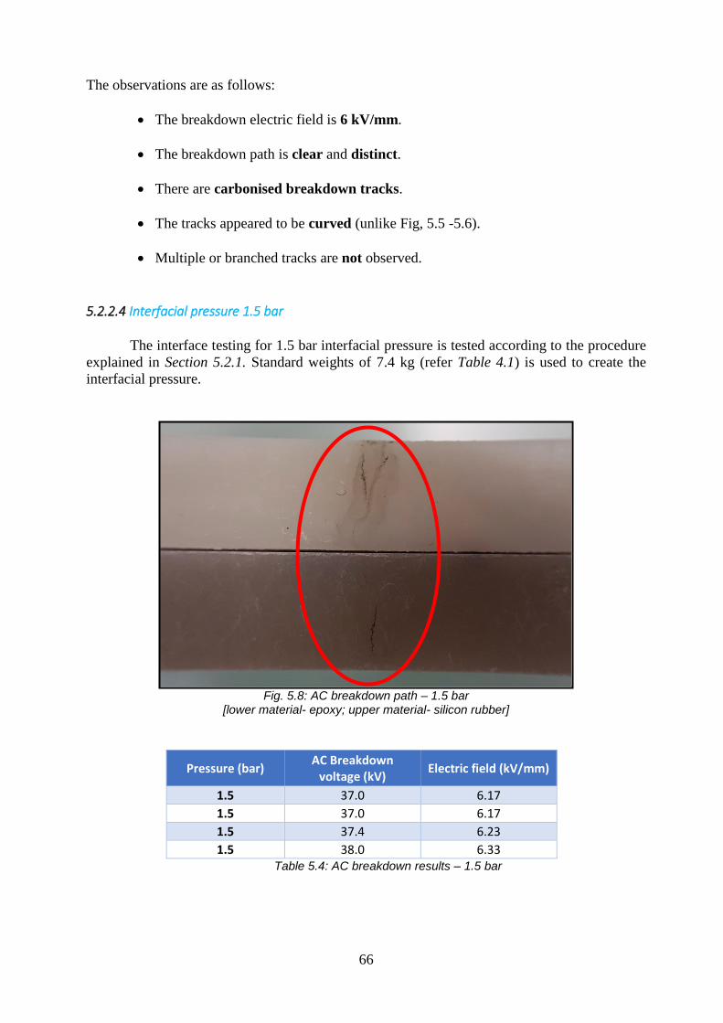
66
The observations are as follows:
• The breakdown electric field is 6 kV/mm.
• The breakdown path is clear and distinct.
• There are carbonised breakdown tracks.
• The tracks appeared to be curved (unlike Fig, 5.5 -5.6).
• Multiple or branched tracks are not observed.
5.2.2.4 Interfacial pressure 1.5 bar
The interface testing for 1.5 bar interfacial pressure is tested according to the procedure
explained in Section 5.2.1. Standard weights of 7.4 kg (refer Table 4.1) is used to create the
interfacial pressure.
Fig. 5.8: AC breakdown path – 1.5 bar
[lower material- epoxy; upper material- silicon rubber]
Pressure (bar) AC Breakdown
voltage (kV) Electric field (kV/mm)
1.5 37.0 6.17
1.5 37.0 6.17
1.5 37.4 6.23
1.5 38.0 6.33 Table 5.4: AC breakdown results – 1.5 bar

67
The observations are as follows:
• The breakdown electric field is around 6.2 kV/mm.
• The breakdown path is clear and distinct.
• There are carbonised breakdown tracks.
• The tracks appeared to be curved (unlike Fig, 5.5 -5.6).
• Multiple or branched tracks are observed in all the samples.
5.2.2.5 Interfacial pressure 2 bar
The interface testing for 2 bar interfacial pressure is tested according to the procedure
explained in Section 5.2.1. Standard weight of 10 kg (refer Table 4.1) is used to create the
interfacial pressure.
Fig. 5.9: AC breakdown path – 2 bar
[lower material- epoxy; upper material- silicon rubber]
Pressure (bar) AC Breakdown
voltage (kV) Electric field (kV/mm)
2.0 40.2 6.69
2.0 40.2 6.69
2.0 40.2 6.69
2.0 40.2 6.69 Table 5.5: AC breakdown results – 2 bar
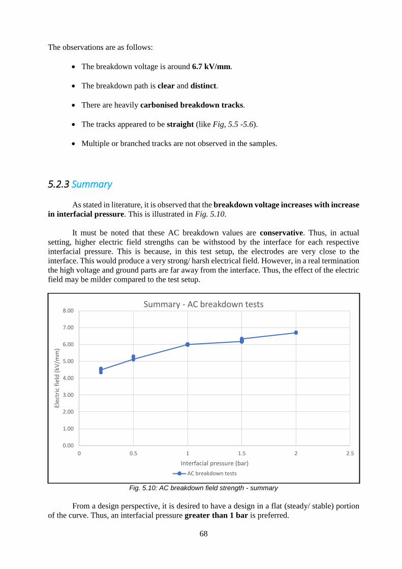
68
The observations are as follows:
• The breakdown voltage is around 6.7 kV/mm.
• The breakdown path is clear and distinct.
• There are heavily carbonised breakdown tracks.
• The tracks appeared to be straight (like Fig, 5.5 -5.6).
• Multiple or branched tracks are not observed in the samples.
5.2.3 Summary
As stated in literature, it is observed that the breakdown voltage increases with increase
in interfacial pressure. This is illustrated in Fig. 5.10.
It must be noted that these AC breakdown values are conservative. Thus, in actual
setting, higher electric field strengths can be withstood by the interface for each respective
interfacial pressure. This is because, in this test setup, the electrodes are very close to the
interface. This would produce a very strong/ harsh electrical field. However, in a real termination
the high voltage and ground parts are far away from the interface. Thus, the effect of the electric
field may be milder compared to the test setup.
Fig. 5.10: AC breakdown field strength - summary
From a design perspective, it is desired to have a design in a flat (steady/ stable) portion
of the curve. Thus, an interfacial pressure greater than 1 bar is preferred.
0.00
1.00
2.00
3.00
4.00
5.00
6.00
7.00
8.00
0 0.5 1 1.5 2 2.5
Elec
tric
fie
ld (
kV/m
m)
Interfacial pressure (bar)
Summary - AC breakdown tests
AC breakdown tests
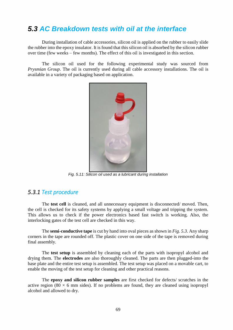
69
5.3 AC Breakdown tests with oil at the interface
During installation of cable accessories, silicon oil is applied on the rubber to easily slide
the rubber into the epoxy insulator. It is found that this silicon oil is absorbed by the silicon rubber
over time (few weeks – few months). The effect of this oil is investigated in this section.
The silicon oil used for the following experimental study was sourced from
Prysmian Group. The oil is currently used during all cable accessory installations. The oil is
available in a variety of packaging based on application.
Fig. 5.11: Silicon oil used as a lubricant during installation
5.3.1 Test procedure
The test cell is cleaned, and all unnecessary equipment is disconnected/ moved. Then,
the cell is checked for its safety systems by applying a small voltage and tripping the system.
This allows us to check if the power electronics based fast switch is working. Also, the
interlocking gates of the test cell are checked in this way.
The semi-conductive tape is cut by hand into oval pieces as shown in Fig. 5.3. Any sharp
corners in the tape are rounded off. The plastic cover on one side of the tape is removed during
final assembly.
The test setup is assembled by cleaning each of the parts with isopropyl alcohol and
drying them. The electrodes are also thoroughly cleaned. The parts are then plugged-into the
base plate and the entire test setup is assembled. The test setup was placed on a movable cart, to
enable the moving of the test setup for cleaning and other practical reasons.
The epoxy and silicon rubber samples are first checked for defects/ scratches in the
active region (80 × 6 mm sides). If no problems are found, they are cleaned using isopropyl
alcohol and allowed to dry.
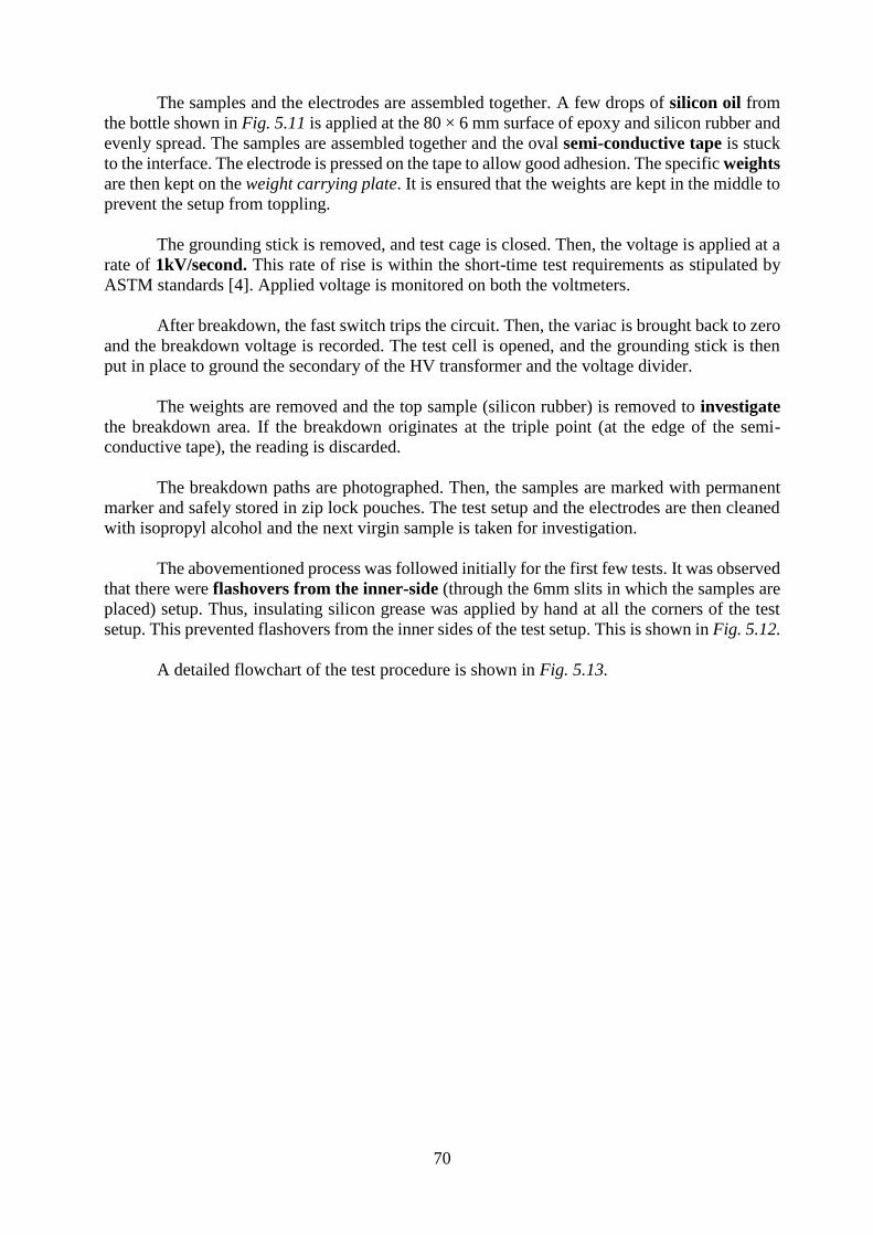
70
The samples and the electrodes are assembled together. A few drops of silicon oil from
the bottle shown in Fig. 5.11 is applied at the 80 × 6 mm surface of epoxy and silicon rubber and
evenly spread. The samples are assembled together and the oval semi-conductive tape is stuck
to the interface. The electrode is pressed on the tape to allow good adhesion. The specific weights
are then kept on the weight carrying plate. It is ensured that the weights are kept in the middle to
prevent the setup from toppling.
The grounding stick is removed, and test cage is closed. Then, the voltage is applied at a
rate of 1kV/second. This rate of rise is within the short-time test requirements as stipulated by
ASTM standards [4]. Applied voltage is monitored on both the voltmeters.
After breakdown, the fast switch trips the circuit. Then, the variac is brought back to zero
and the breakdown voltage is recorded. The test cell is opened, and the grounding stick is then
put in place to ground the secondary of the HV transformer and the voltage divider.
The weights are removed and the top sample (silicon rubber) is removed to investigate
the breakdown area. If the breakdown originates at the triple point (at the edge of the semi-
conductive tape), the reading is discarded.
The breakdown paths are photographed. Then, the samples are marked with permanent
marker and safely stored in zip lock pouches. The test setup and the electrodes are then cleaned
with isopropyl alcohol and the next virgin sample is taken for investigation.
The abovementioned process was followed initially for the first few tests. It was observed
that there were flashovers from the inner-side (through the 6mm slits in which the samples are
placed) setup. Thus, insulating silicon grease was applied by hand at all the corners of the test
setup. This prevented flashovers from the inner sides of the test setup. This is shown in Fig. 5.12.
A detailed flowchart of the test procedure is shown in Fig. 5.13.
71
Fig. 5.12: Silicon grease used to prevent inner-side flashovers
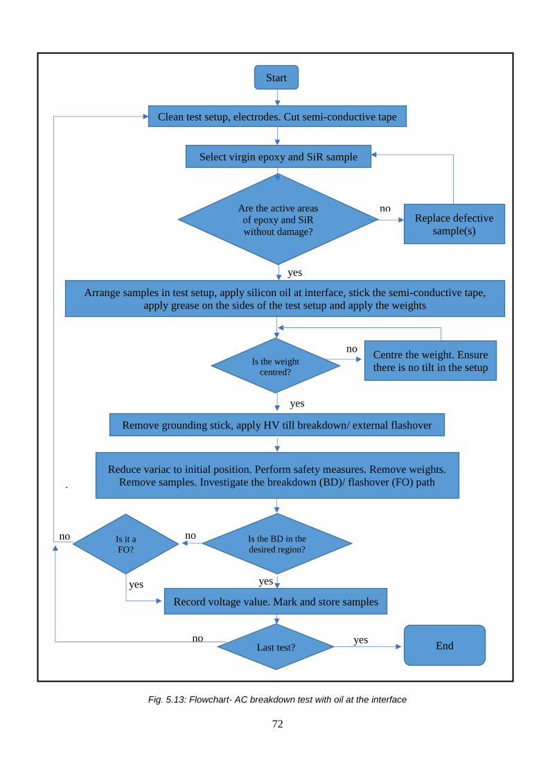
72
.
Fig. 5.13: Flowchart- AC breakdown test with oil at the interface
Start
Clean test setup, electrodes. Cut semi-conductive tape
Are the active areas
of epoxy and SiR
without damage?
Arrange samples in test setup, apply silicon oil at interface, stick the semi-conductive tape,
apply grease on the sides of the test setup and apply the weights
Is the weight
centred?
no Replace defective
sample(s)
Select virgin epoxy and SiR sample
yes
Remove grounding stick, apply HV till breakdown/ external flashover
Centre the weight. Ensure
there is no tilt in the setup
Reduce variac to initial position. Perform safety measures. Remove weights.
Remove samples. Investigate the breakdown (BD)/ flashover (FO) path
Is the BD in the
desired region?
Record voltage value. Mark and store samples
Last test? End
yes
no
yes no
no
yes
Is it a
FO?
no
yes
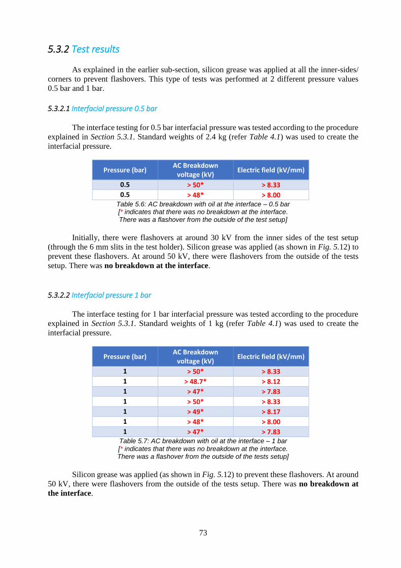
73
5.3.2 Test results
As explained in the earlier sub-section, silicon grease was applied at all the inner-sides/
corners to prevent flashovers. This type of tests was performed at 2 different pressure values
0.5 bar and 1 bar.
5.3.2.1 Interfacial pressure 0.5 bar
The interface testing for 0.5 bar interfacial pressure was tested according to the procedure
explained in Section 5.3.1. Standard weights of 2.4 kg (refer Table 4.1) was used to create the
interfacial pressure.
Pressure (bar) AC Breakdown
voltage (kV) Electric field (kV/mm)
0.5 > 50* > 8.33
0.5 > 48* > 8.00 Table 5.6: AC breakdown with oil at the interface – 0.5 bar [* indicates that there was no breakdown at the interface. There was a flashover from the outside of the test setup]
Initially, there were flashovers at around 30 kV from the inner sides of the test setup
(through the 6 mm slits in the test holder). Silicon grease was applied (as shown in Fig. 5.12) to
prevent these flashovers. At around 50 kV, there were flashovers from the outside of the tests
setup. There was no breakdown at the interface.
5.3.2.2 Interfacial pressure 1 bar
The interface testing for 1 bar interfacial pressure was tested according to the procedure
explained in Section 5.3.1. Standard weights of 1 kg (refer Table 4.1) was used to create the
interfacial pressure.
Pressure (bar) AC Breakdown
voltage (kV) Electric field (kV/mm)
1 > 50* > 8.33
1 > 48.7* > 8.12
1 > 47* > 7.83
1 > 50* > 8.33
1 > 49* > 8.17
1 > 48* > 8.00
1 > 47* > 7.83 Table 5.7: AC breakdown with oil at the interface – 1 bar [* indicates that there was no breakdown at the interface. There was a flashover from the outside of the tests setup]
Silicon grease was applied (as shown in Fig. 5.12) to prevent these flashovers. At around
50 kV, there were flashovers from the outside of the tests setup. There was no breakdown at
the interface.
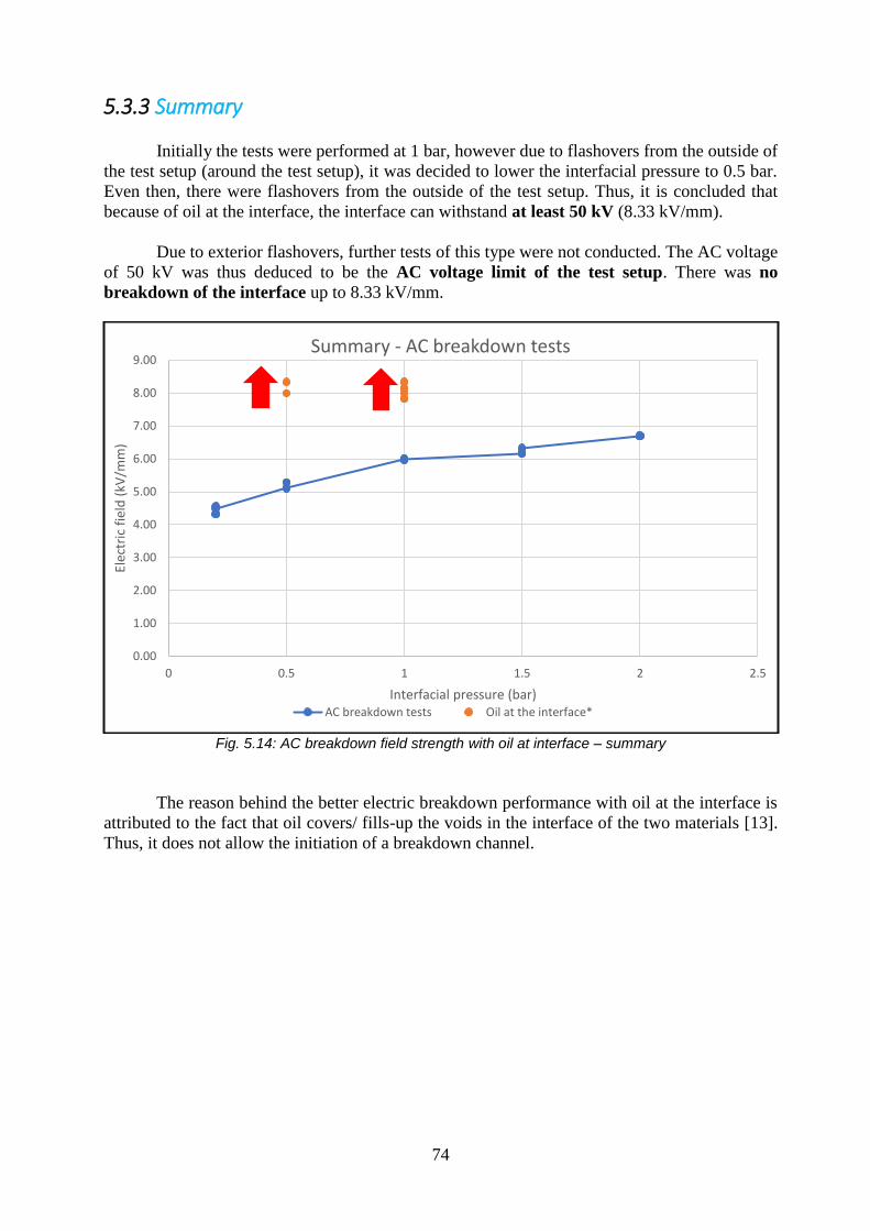
74
5.3.3 Summary
Initially the tests were performed at 1 bar, however due to flashovers from the outside of
the test setup (around the test setup), it was decided to lower the interfacial pressure to 0.5 bar.
Even then, there were flashovers from the outside of the test setup. Thus, it is concluded that
because of oil at the interface, the interface can withstand at least 50 kV (8.33 kV/mm).
Due to exterior flashovers, further tests of this type were not conducted. The AC voltage
of 50 kV was thus deduced to be the AC voltage limit of the test setup. There was no
breakdown of the interface up to 8.33 kV/mm.
Fig. 5.14: AC breakdown field strength with oil at interface – summary
The reason behind the better electric breakdown performance with oil at the interface is
attributed to the fact that oil covers/ fills-up the voids in the interface of the two materials [13].
Thus, it does not allow the initiation of a breakdown channel.
0.00
1.00
2.00
3.00
4.00
5.00
6.00
7.00
8.00
9.00
0 0.5 1 1.5 2 2.5
Elec
tric
fie
ld (
kV/m
m)
Interfacial pressure (bar)
Summary - AC breakdown tests
AC breakdown tests Oil at the interface*
75
5.4 AC breakdown tests with scratch on epoxy
During the installation of accessories, it is sometimes observed that there can be some
scratches on the epoxy surface. Although it is rare, it is attributed to improper installation/
mounting techniques. Also, sometimes installation tools may scratch the surface of the epoxy.
This section aims to find the effect of such scratches on the electrical performance of the epoxy/
silicon rubber interface. Single scratches are made by using a knife. The scratches are made
parallel and perpendicular to the applied electric field.
5.4.1 Test procedure
The test cell is cleaned, and all unnecessary equipment is disconnected/ moved. Then,
the cell is checked for its safety systems by applying a small voltage and tripping the system.
This allows us to check if the power electronics based fast switch is working. Also, the
interlocking gates of the test cell are checked in this way.
The semi-conductive tape is cut by hand into oval pieces as shown in Fig. 5.3. Any sharp
corners in the tape are rounded off. The plastic cover on one side of the tape is removed during
final assembly.
The test setup is assembled by cleaning each of the parts with isopropyl alcohol and
drying them. The electrodes are also thoroughly cleaned. The parts are then plugged-into the
base plate and the entire test setup is assembled. The test setup was placed on a movable cart, to
enable the moving of the test setup for cleaning and other practical reasons.
The epoxy and silicon rubber samples are first checked for manufacturing defects/
scratches in the active region (80 × 6 mm sides). A scratch is made using a knife. The samples
are then cleaned using isopropyl alcohol and allowed to dry.
The oval semi-conductive tape is stuck to the interface and then the electrode is pressed
on the tape to allow good adhesion. The specific weights are then kept on the weight carrying
plate. It is ensured that the weights are kept in the middle to prevent the setup from toppling.
The grounding stick is removed, and test cage is closed. Then, the voltage is applied at a
rate of 1kV/second. This rate of rise is within the short-time test requirements as stipulated by
ASTM standards [4]. Applied voltage is monitored on both the voltmeters.
After breakdown, the fast switch trips the circuit. Then, the variac is brought back to zero
and the breakdown voltage is recorded. The test cell is opened, and the grounding stick is then
put in place to ground the secondary of the HV transformer and the voltage divider.
The weights are removed and the top sample (silicon rubber) is removed to investigate
the breakdown area. If the breakdown originates at the triple point (at the edge of the semi-
conductive tape), the reading is discarded.
The breakdown paths are photographed. Then, the samples are marked with permanent
marker and safely stored in zip lock pouches. The test setup and the electrodes are then cleaned
with isopropyl alcohol and the next virgin sample is taken for investigation.
A detailed flowchart of the test procedure is shown in Fig. 5.15.

76
.
Fig. 5.15: Flowchart- AC breakdown test with scratch on epoxy
Start
Clean test setup, electrodes. Cut semi-conductive tape
Arrange samples in test setup, stick the semi-conductive tape, and apply the weights
Is the weight
centred?
Scratch epoxy sample with a sharp knife
Select virgin epoxy and SiR samples
yes
Remove grounding stick, apply HV till breakdown
Centre the weight. Ensure
there is no tilt in the setup
Reduce variac to initial position. Perform safety measures. Remove weights.
Remove samples. Investigate the breakdown path
Is the BD in the
desired region?
Record BD value. Mark and store samples
Last test? End
yes
no
yes no
no
Clean samples with alcohol
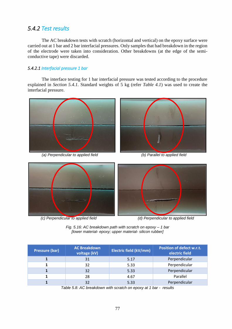
77
5.4.2 Test results
The AC breakdown tests with scratch (horizontal and vertical) on the epoxy surface were
carried out at 1 bar and 2 bar interfacial pressures. Only samples that had breakdown in the region
of the electrode were taken into consideration. Other breakdowns (at the edge of the semi-
conductive tape) were discarded.
5.4.2.1 Interfacial pressure 1 bar
The interface testing for 1 bar interfacial pressure was tested according to the procedure
explained in Section 5.4.1. Standard weights of 5 kg (refer Table 4.1) was used to create the
interfacial pressure.
(a) Perpendicular to applied field (b) Parallel to applied field
(c) Perpendicular to applied field (d) Perpendicular to applied field
Fig. 5.16: AC breakdown path with scratch on epoxy – 1 bar
[lower material- epoxy; upper material- silicon rubber]
Pressure (bar) AC Breakdown
voltage (kV) Electric field (kV/mm)
Position of defect w.r.t. electric field
1 31 5.17 Perpendicular
1 32 5.33 Perpendicular
1 32 5.33 Perpendicular
1 28 4.67 Parallel
1 32 5.33 Perpendicular
Table 5.8: AC breakdown with scratch on epoxy at 1 bar - results
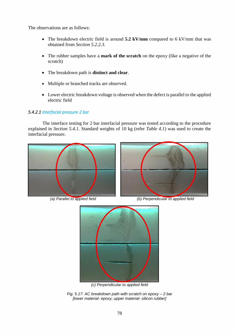
78
The observations are as follows:
• The breakdown electric field is around 5.2 kV/mm compared to 6 kV/mm that was
obtained from Section 5.2.2.3.
• The rubber samples have a mark of the scratch on the epoxy (like a negative of the
scratch)
• The breakdown path is distinct and clear.
• Multiple or branched tracks are observed.
• Lower electric breakdown voltage is observed when the defect is parallel to the applied
electric field
5.4.2.1 Interfacial pressure 2 bar
The interface testing for 2 bar interfacial pressure was tested according to the procedure
explained in Section 5.4.1. Standard weights of 10 kg (refer Table 4.1) was used to create the
interfacial pressure.
(a) Parallel to applied field (b) Perpendicular to applied field
(c) Perpendicular to applied field
Fig. 5.17: AC breakdown path with scratch on epoxy – 2 bar [lower material- epoxy; upper material- silicon rubber]
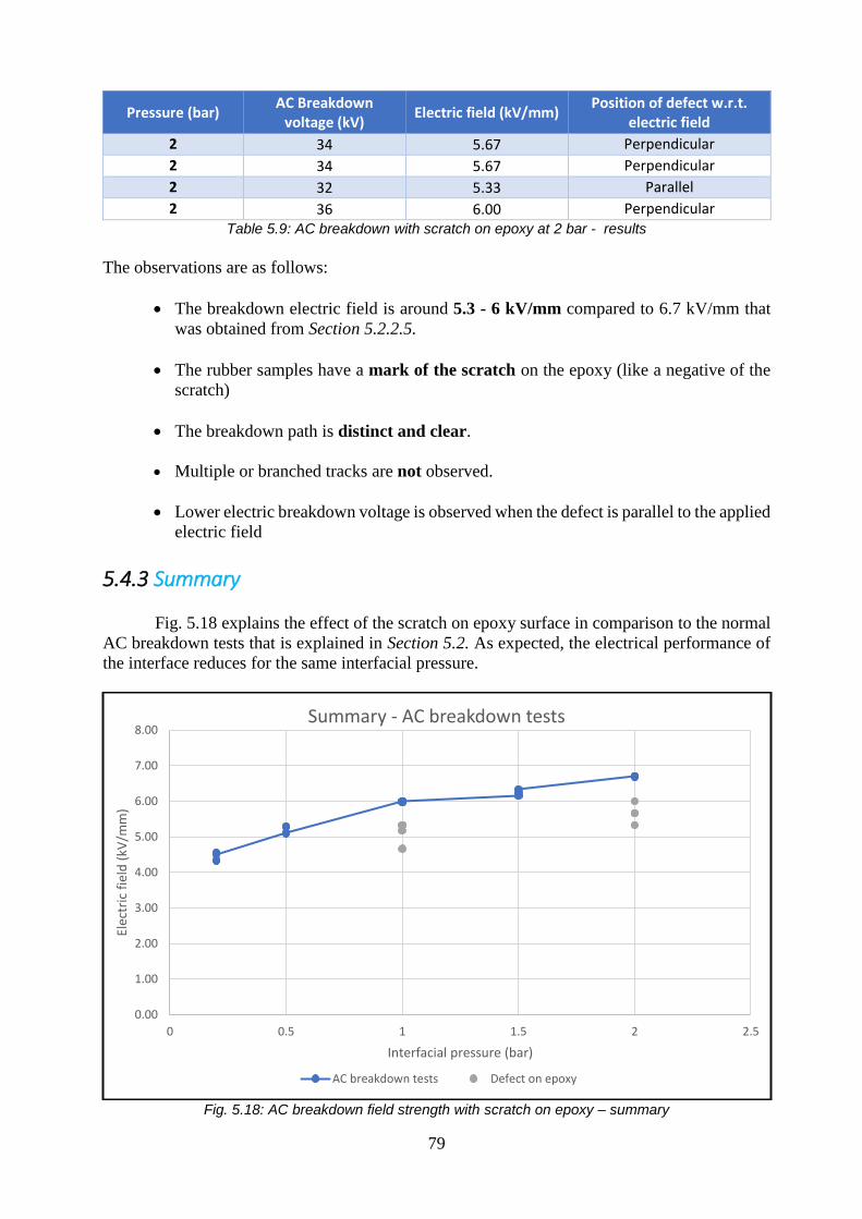
79
Pressure (bar) AC Breakdown
voltage (kV) Electric field (kV/mm)
Position of defect w.r.t. electric field
2 34 5.67 Perpendicular
2 34 5.67 Perpendicular
2 32 5.33 Parallel
2 36 6.00 Perpendicular Table 5.9: AC breakdown with scratch on epoxy at 2 bar - results
The observations are as follows:
• The breakdown electric field is around 5.3 - 6 kV/mm compared to 6.7 kV/mm that
was obtained from Section 5.2.2.5.
• The rubber samples have a mark of the scratch on the epoxy (like a negative of the
scratch)
• The breakdown path is distinct and clear.
• Multiple or branched tracks are not observed.
• Lower electric breakdown voltage is observed when the defect is parallel to the applied
electric field
5.4.3 Summary
Fig. 5.18 explains the effect of the scratch on epoxy surface in comparison to the normal
AC breakdown tests that is explained in Section 5.2. As expected, the electrical performance of
the interface reduces for the same interfacial pressure.
Fig. 5.18: AC breakdown field strength with scratch on epoxy – summary
0.00
1.00
2.00
3.00
4.00
5.00
6.00
7.00
8.00
0 0.5 1 1.5 2 2.5
Elec
tric
fie
ld (
kV/m
m)
Interfacial pressure (bar)
Summary - AC breakdown tests
AC breakdown tests Defect on epoxy
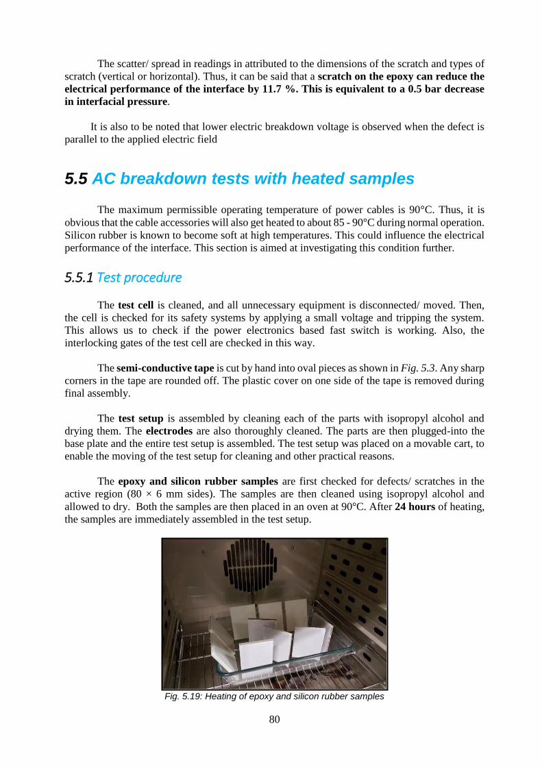
80
The scatter/ spread in readings in attributed to the dimensions of the scratch and types of
scratch (vertical or horizontal). Thus, it can be said that a scratch on the epoxy can reduce the
electrical performance of the interface by 11.7 %. This is equivalent to a 0.5 bar decrease
in interfacial pressure.
It is also to be noted that lower electric breakdown voltage is observed when the defect is
parallel to the applied electric field
5.5 AC breakdown tests with heated samples
The maximum permissible operating temperature of power cables is 90°C. Thus, it is
obvious that the cable accessories will also get heated to about 85 - 90°C during normal operation.
Silicon rubber is known to become soft at high temperatures. This could influence the electrical
performance of the interface. This section is aimed at investigating this condition further.
5.5.1 Test procedure
The test cell is cleaned, and all unnecessary equipment is disconnected/ moved. Then,
the cell is checked for its safety systems by applying a small voltage and tripping the system.
This allows us to check if the power electronics based fast switch is working. Also, the
interlocking gates of the test cell are checked in this way.
The semi-conductive tape is cut by hand into oval pieces as shown in Fig. 5.3. Any sharp
corners in the tape are rounded off. The plastic cover on one side of the tape is removed during
final assembly.
The test setup is assembled by cleaning each of the parts with isopropyl alcohol and
drying them. The electrodes are also thoroughly cleaned. The parts are then plugged-into the
base plate and the entire test setup is assembled. The test setup was placed on a movable cart, to
enable the moving of the test setup for cleaning and other practical reasons.
The epoxy and silicon rubber samples are first checked for defects/ scratches in the
active region (80 × 6 mm sides). The samples are then cleaned using isopropyl alcohol and
allowed to dry. Both the samples are then placed in an oven at 90°C. After 24 hours of heating,
the samples are immediately assembled in the test setup.
Fig. 5.19: Heating of epoxy and silicon rubber samples
81
The oval semi-conductive tape is stuck to the interface and then the electrode is pressed
on the tape to allow good adhesion. The specific weights are then kept on the weight carrying
plate. It is ensured that the weights are kept in the middle to prevent the setup from toppling.
The grounding stick is removed, and test cage is closed. Then, the voltage is applied at a
rate of 1kV/second. This rate of rise is within the short-time test requirements as stipulated by
ASTM standards [4]. Applied voltage is monitored on both the voltmeters.
After breakdown, the fast switch trips the circuit. Then, the variac is brought back to zero
and the breakdown voltage is recorded. The test cell is opened, and the grounding stick is then
put in place to ground the secondary of the HV transformer and the voltage divider.
The weights are removed and the top sample (silicon rubber) is removed to investigate
the breakdown area. If the breakdown originates at the triple point (at the edge of the semi-
conductive tape), the reading is discarded.
The breakdown paths are photographed. Then, the samples are marked with permanent
marker and safely stored in zip lock pouches. The test setup and the electrodes are then cleaned
with isopropyl alcohol and the next virgin sample is taken for investigation.
A detailed flowchart of the test procedure is shown in Fig. 5.20.
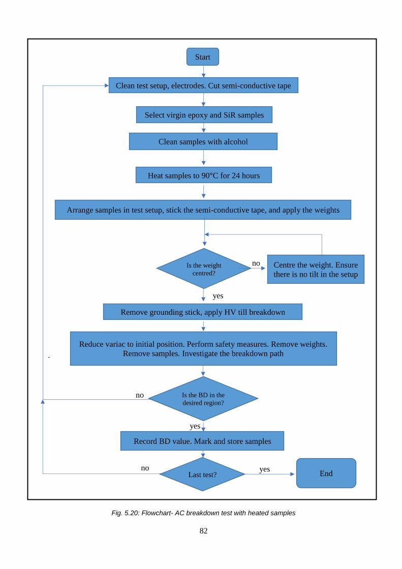
82
.
Fig. 5.20: Flowchart- AC breakdown test with heated samples
Start
Clean test setup, electrodes. Cut semi-conductive tape
Arrange samples in test setup, stick the semi-conductive tape, and apply the weights
Is the weight
centred?
Clean samples with alcohol
Select virgin epoxy and SiR samples
yes
Remove grounding stick, apply HV till breakdown
Centre the weight. Ensure
there is no tilt in the setup
Reduce variac to initial position. Perform safety measures. Remove weights.
Remove samples. Investigate the breakdown path
Is the BD in the
desired region?
Record BD value. Mark and store samples
Last test? End
yes
no
yes no
no
Heat samples to 90°C for 24 hours
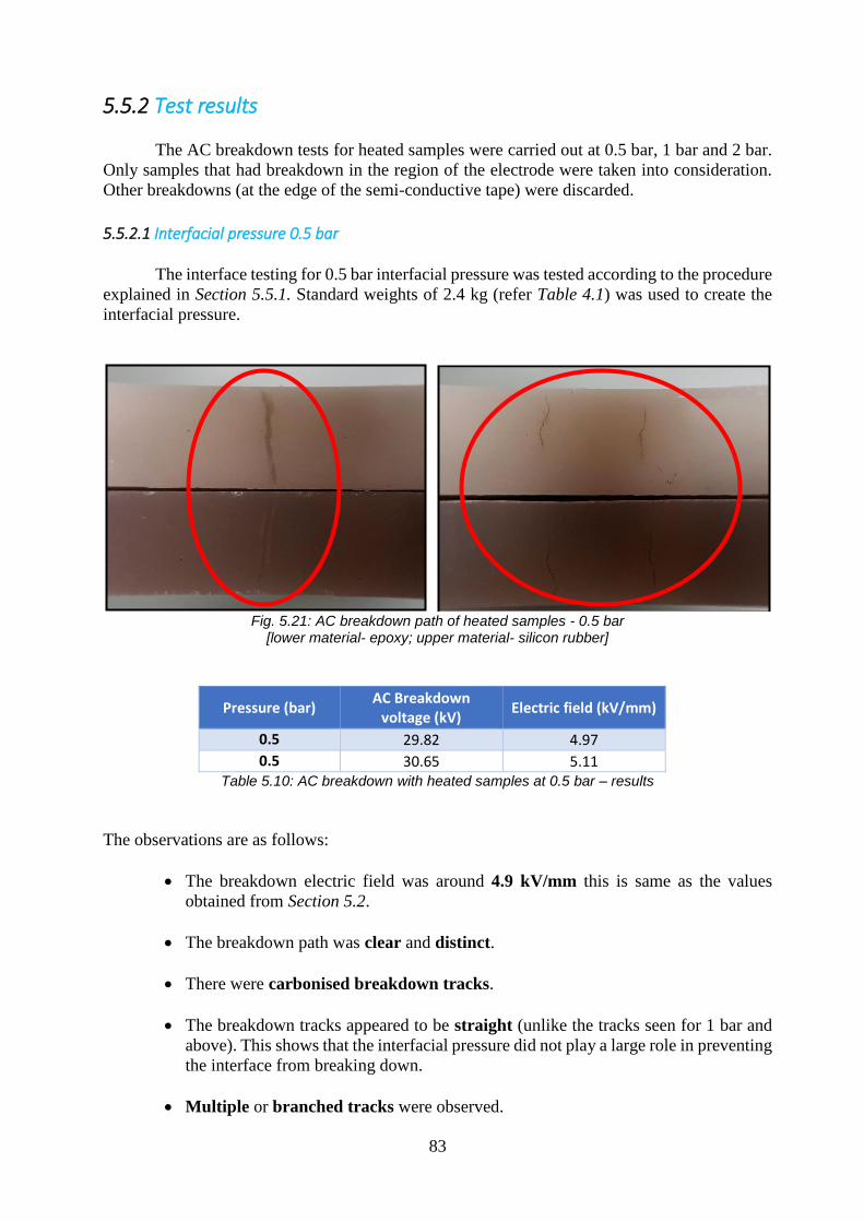
83
5.5.2 Test results
The AC breakdown tests for heated samples were carried out at 0.5 bar, 1 bar and 2 bar.
Only samples that had breakdown in the region of the electrode were taken into consideration.
Other breakdowns (at the edge of the semi-conductive tape) were discarded.
5.5.2.1 Interfacial pressure 0.5 bar
The interface testing for 0.5 bar interfacial pressure was tested according to the procedure
explained in Section 5.5.1. Standard weights of 2.4 kg (refer Table 4.1) was used to create the
interfacial pressure.
Fig. 5.21: AC breakdown path of heated samples - 0.5 bar
[lower material- epoxy; upper material- silicon rubber]
Pressure (bar) AC Breakdown
voltage (kV) Electric field (kV/mm)
0.5 29.82 4.97
0.5 30.65 5.11 Table 5.10: AC breakdown with heated samples at 0.5 bar – results
The observations are as follows:
• The breakdown electric field was around 4.9 kV/mm this is same as the values
obtained from Section 5.2.
• The breakdown path was clear and distinct.
• There were carbonised breakdown tracks.
• The breakdown tracks appeared to be straight (unlike the tracks seen for 1 bar and
above). This shows that the interfacial pressure did not play a large role in preventing
the interface from breaking down.
• Multiple or branched tracks were observed.
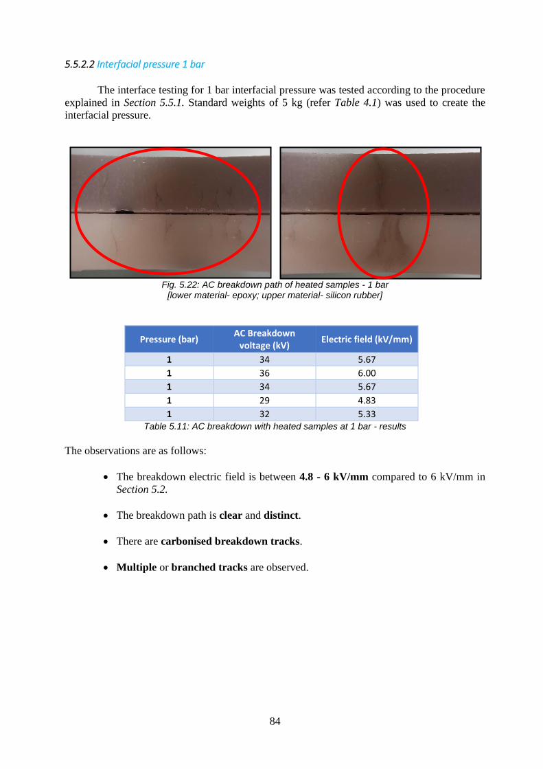
84
5.5.2.2 Interfacial pressure 1 bar
The interface testing for 1 bar interfacial pressure was tested according to the procedure
explained in Section 5.5.1. Standard weights of 5 kg (refer Table 4.1) was used to create the
interfacial pressure.
Fig. 5.22: AC breakdown path of heated samples - 1 bar
[lower material- epoxy; upper material- silicon rubber]
Pressure (bar) AC Breakdown
voltage (kV) Electric field (kV/mm)
1 34 5.67
1 36 6.00
1 34 5.67
1 29 4.83
1 32 5.33 Table 5.11: AC breakdown with heated samples at 1 bar - results
The observations are as follows:
• The breakdown electric field is between 4.8 - 6 kV/mm compared to 6 kV/mm in
Section 5.2.
• The breakdown path is clear and distinct.
• There are carbonised breakdown tracks.
• Multiple or branched tracks are observed.
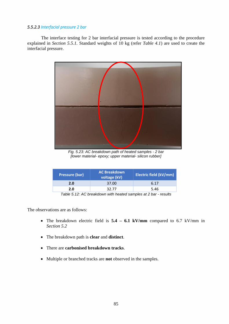
85
5.5.2.3 Interfacial pressure 2 bar
The interface testing for 2 bar interfacial pressure is tested according to the procedure
explained in Section 5.5.1. Standard weights of 10 kg (refer Table 4.1) are used to create the
interfacial pressure.
Fig. 5.23: AC breakdown path of heated samples - 2 bar
[lower material- epoxy; upper material- silicon rubber]
Pressure (bar) AC Breakdown
voltage (kV) Electric field (kV/mm)
2.0 37.00 6.17
2.0 32.77 5.46 Table 5.12: AC breakdown with heated samples at 2 bar - results
The observations are as follows:
• The breakdown electric field is 5.4 – 6.1 kV/mm compared to 6.7 kV/mm in
Section 5.2
• The breakdown path is clear and distinct.
• There are carbonised breakdown tracks.
• Multiple or branched tracks are not observed in the samples.
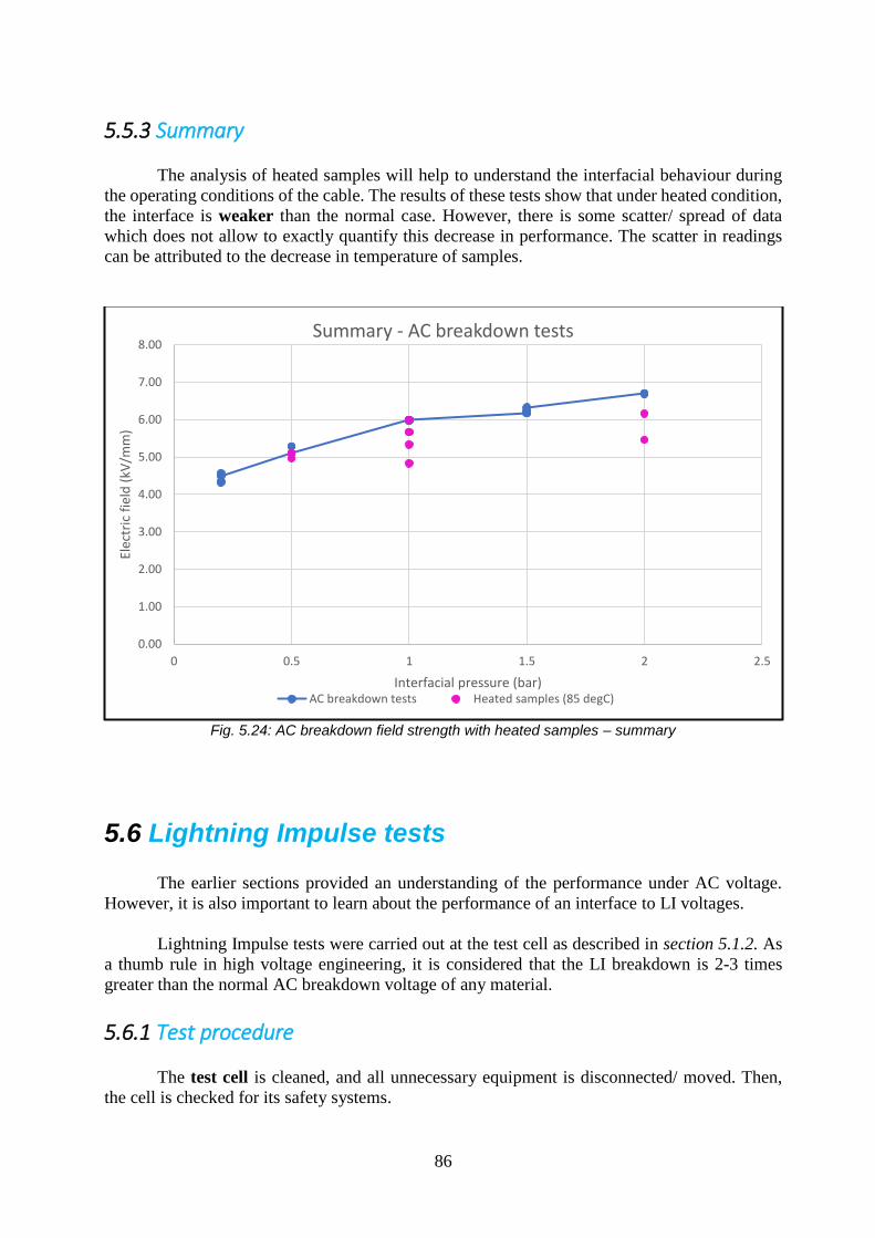
86
5.5.3 Summary
The analysis of heated samples will help to understand the interfacial behaviour during
the operating conditions of the cable. The results of these tests show that under heated condition,
the interface is weaker than the normal case. However, there is some scatter/ spread of data
which does not allow to exactly quantify this decrease in performance. The scatter in readings
can be attributed to the decrease in temperature of samples.
Fig. 5.24: AC breakdown field strength with heated samples – summary
5.6 Lightning Impulse tests
The earlier sections provided an understanding of the performance under AC voltage.
However, it is also important to learn about the performance of an interface to LI voltages.
Lightning Impulse tests were carried out at the test cell as described in section 5.1.2. As
a thumb rule in high voltage engineering, it is considered that the LI breakdown is 2-3 times
greater than the normal AC breakdown voltage of any material.
5.6.1 Test procedure
The test cell is cleaned, and all unnecessary equipment is disconnected/ moved. Then,
the cell is checked for its safety systems.
0.00
1.00
2.00
3.00
4.00
5.00
6.00
7.00
8.00
0 0.5 1 1.5 2 2.5
Elec
tric
fie
ld (
kV/m
m)
Interfacial pressure (bar)
Summary - AC breakdown tests
AC breakdown tests Heated samples (85 degC)
87
The semi-conductive tape is cut by hand into oval pieces as shown in Fig. 5.3. Any sharp
corners in the tape are rounded off. The plastic cover on one side of the tape is removed during
final assembly.
The test setup is assembled by cleaning each of the parts with isopropyl alcohol and
drying them. The electrodes are also thoroughly cleaned. The parts are then plugged-into the
base plate and the entire test setup is assembled. The test setup was placed on a movable cart, to
enable the moving of the test setup for cleaning and other practical reasons.
The epoxy and silicon rubber samples are first checked for defects/ scratches in the
active region (80 × 6 mm sides). The samples are then cleaned using isopropyl alcohol.
The oval semi-conductive tape is stuck to the interface and then the electrode is pressed
on the tape to allow good adhesion. The specific weights are then kept on the weight carrying
plate. It is ensured that the weights are kept in the middle to prevent the setup from toppling.
After a few initial tests it was observed that there were flashovers from the inner side of
the test setup (through the 6 mm slit). Thus, silicon grease was applied to all the corners to
prevent flashovers from the inner sides (refer Fig. 5.12).
The test cage is closed. Then, a voltage of 40 kV is applied using the impulse analysing
and control system. The system gives a plot of the applied voltage. This helps us to know if there
was a breakdown. Voltage is increased in steps of 10kV until there is a breakdown/ flashover.
After breakdown/ flashover, the impulse analysing system plots the front-chopped or tail-
chopped waveform. The system is automatically grounded.
The weights are removed and the top sample (silicon rubber) is removed to investigate
the breakdown area. If the breakdown originates at the triple point (at the edge of the semi-
conductive tape), the reading is discarded.
The breakdown paths are photographed. Then, the samples are marked with permanent
marker and safely stored in zip lock pouches. The test setup and the electrodes are then cleaned
with isopropyl alcohol and the next virgin sample is taken for investigation.
A detailed flowchart of the test procedure is shown in Fig. 5.25.
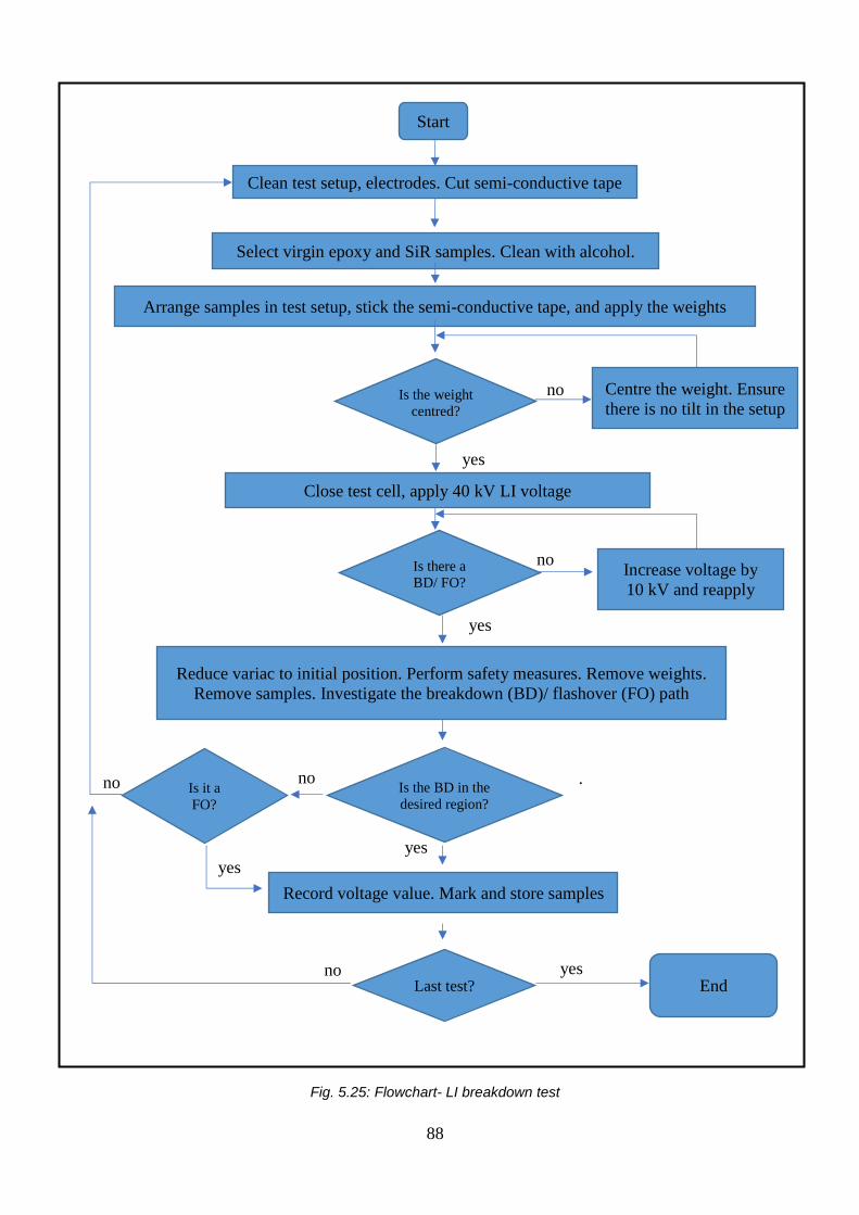
88
.
Fig. 5.25: Flowchart- LI breakdown test
Start
Clean test setup, electrodes. Cut semi-conductive tape
Arrange samples in test setup, stick the semi-conductive tape, and apply the weights
Is the weight
centred?
Select virgin epoxy and SiR samples. Clean with alcohol.
yes
Close test cell, apply 40 kV LI voltage
Centre the weight. Ensure
there is no tilt in the setup
End yes
no
Is there a
BD/ FO?
yes
no Increase voltage by
10 kV and reapply
Reduce variac to initial position. Perform safety measures. Remove weights.
Remove samples. Investigate the breakdown (BD)/ flashover (FO) path
Is the BD in the
desired region?
Record voltage value. Mark and store samples
Last test?
yes
no
no
Is it a
FO?
no
yes
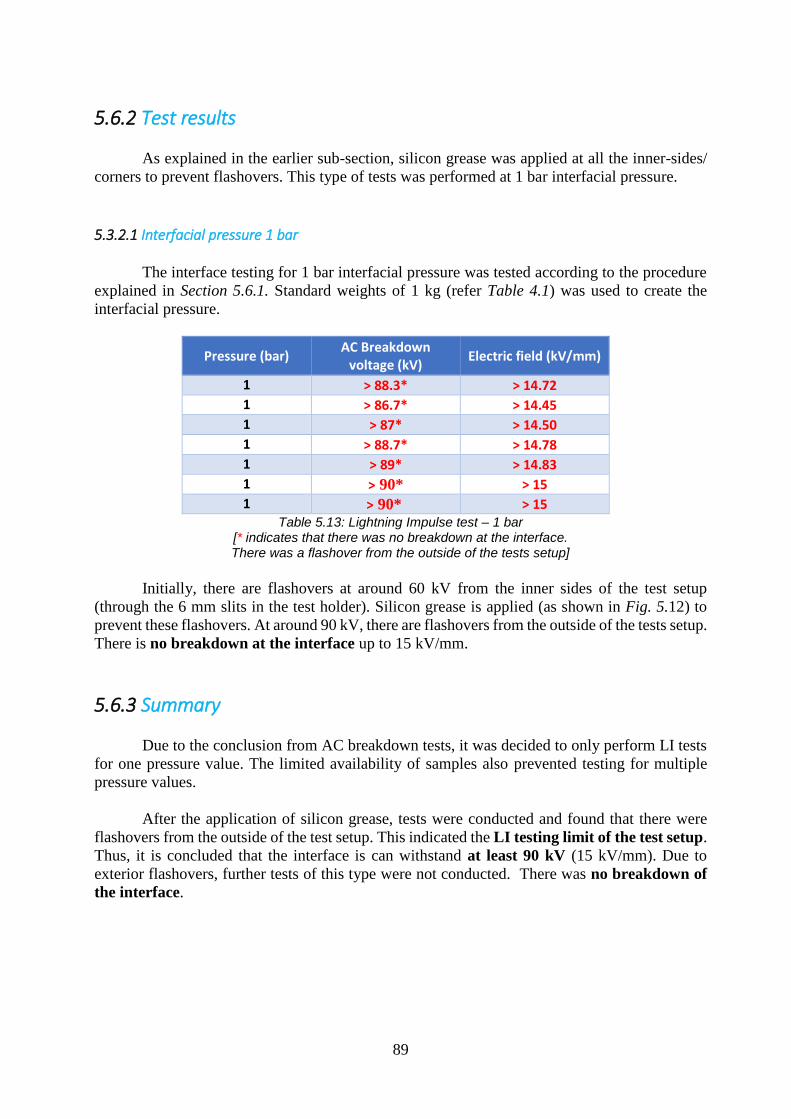
89
5.6.2 Test results
As explained in the earlier sub-section, silicon grease was applied at all the inner-sides/
corners to prevent flashovers. This type of tests was performed at 1 bar interfacial pressure.
5.3.2.1 Interfacial pressure 1 bar
The interface testing for 1 bar interfacial pressure was tested according to the procedure
explained in Section 5.6.1. Standard weights of 1 kg (refer Table 4.1) was used to create the
interfacial pressure.
Pressure (bar) AC Breakdown
voltage (kV) Electric field (kV/mm)
1 > 88.3* > 14.72
1 > 86.7* > 14.45
1 > 87* > 14.50
1 > 88.7* > 14.78
1 > 89* > 14.83
1 > 90* > 15
1 > 90* > 15 Table 5.13: Lightning Impulse test – 1 bar
[* indicates that there was no breakdown at the interface. There was a flashover from the outside of the tests setup]
Initially, there are flashovers at around 60 kV from the inner sides of the test setup
(through the 6 mm slits in the test holder). Silicon grease is applied (as shown in Fig. 5.12) to
prevent these flashovers. At around 90 kV, there are flashovers from the outside of the tests setup.
There is no breakdown at the interface up to 15 kV/mm.
5.6.3 Summary
Due to the conclusion from AC breakdown tests, it was decided to only perform LI tests
for one pressure value. The limited availability of samples also prevented testing for multiple
pressure values.
After the application of silicon grease, tests were conducted and found that there were
flashovers from the outside of the test setup. This indicated the LI testing limit of the test setup.
Thus, it is concluded that the interface is can withstand at least 90 kV (15 kV/mm). Due to
exterior flashovers, further tests of this type were not conducted. There was no breakdown of
the interface.
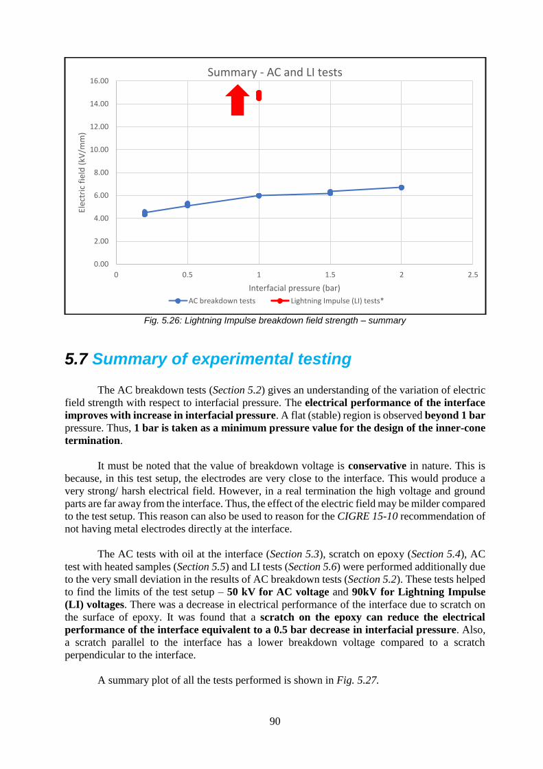
90
Fig. 5.26: Lightning Impulse breakdown field strength – summary
5.7 Summary of experimental testing
The AC breakdown tests (Section 5.2) gives an understanding of the variation of electric
field strength with respect to interfacial pressure. The electrical performance of the interface
improves with increase in interfacial pressure. A flat (stable) region is observed beyond 1 bar
pressure. Thus, 1 bar is taken as a minimum pressure value for the design of the inner-cone
termination.
It must be noted that the value of breakdown voltage is conservative in nature. This is
because, in this test setup, the electrodes are very close to the interface. This would produce a
very strong/ harsh electrical field. However, in a real termination the high voltage and ground
parts are far away from the interface. Thus, the effect of the electric field may be milder compared
to the test setup. This reason can also be used to reason for the CIGRE 15-10 recommendation of
not having metal electrodes directly at the interface.
The AC tests with oil at the interface (Section 5.3), scratch on epoxy (Section 5.4), AC
test with heated samples (Section 5.5) and LI tests (Section 5.6) were performed additionally due
to the very small deviation in the results of AC breakdown tests (Section 5.2). These tests helped
to find the limits of the test setup – 50 kV for AC voltage and 90kV for Lightning Impulse
(LI) voltages. There was a decrease in electrical performance of the interface due to scratch on
the surface of epoxy. It was found that a scratch on the epoxy can reduce the electrical
performance of the interface equivalent to a 0.5 bar decrease in interfacial pressure. Also,
a scratch parallel to the interface has a lower breakdown voltage compared to a scratch
perpendicular to the interface.
A summary plot of all the tests performed is shown in Fig. 5.27.
0.00
2.00
4.00
6.00
8.00
10.00
12.00
14.00
16.00
0 0.5 1 1.5 2 2.5
Elec
tric
fie
ld (
kV/m
m)
Interfacial pressure (bar)
Summary - AC and LI tests
AC breakdown tests Lightning Impulse (LI) tests*
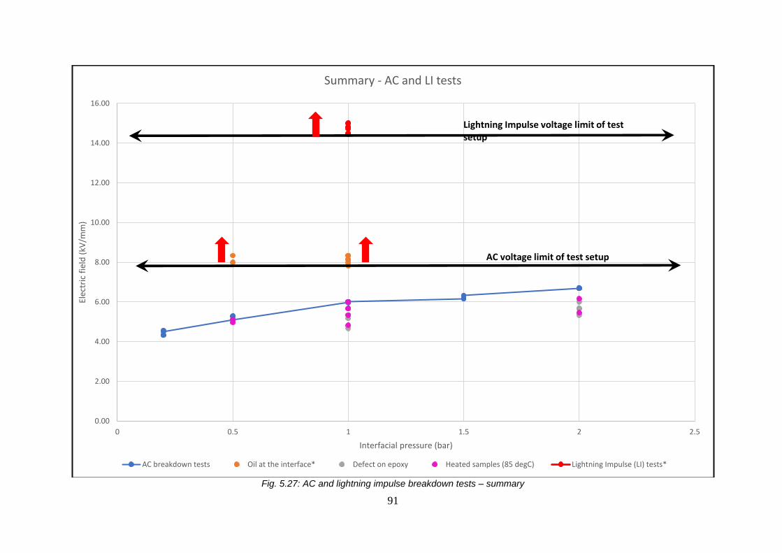
91
Fig. 5.27: AC and lightning impulse breakdown tests – summary
0.00
2.00
4.00
6.00
8.00
10.00
12.00
14.00
16.00
0 0.5 1 1.5 2 2.5
Elec
tric
fie
ld (
kV/m
m)
Interfacial pressure (bar)
Summary - AC and LI tests
AC breakdown tests Oil at the interface* Defect on epoxy Heated samples (85 degC) Lightning Impulse (LI) tests*
Lightning Impulse voltage limit of test setup
AC voltage limit of test setup

92
93
6. Design of GIS termination
This chapter starts with an overview of the CIGRE JWG design of GIS termination. Next, it
introduces the two proposed designs (named ‘A’ and ‘B’) of the 145kV inner-cone GIS cable
termination. Electrical and Mechanical features of the two designs are also presented.
94
6.1 CIGRE JWG design
The CIGRE JWG B1 – B3.49 [49] has been setup to propose a standardised design for the
145 kV inner-cone GIS cable termination. This standardised design will be used as a foundation
by various cable accessory manufacturers to design their termination. The design recommended
by the CIGRE JWG is shown in Fig. 6.1.
The new CIGRE design has the following features:
1. The mechanical connection interface is the M16 x X screw at the top of the integrated
electrode in the GIS.
2. The electrical connection interface is at the top of the ϕ95 mm upper surface of the
integrated electrode. This surface will be silver plated. (marked with red dashed line
in Fig. 6.1).
3. The integrated electrode provides a shielded cavity to have the cable locking
mechanism. By providing this cylindrical volume, the standard allows different
manufacturers to adapt or modify their respective cable locking mechanisms to fit into
this volume.
4. The epoxy/ silicon rubber interface (marked in blue dashed line in Fig. 6.1) starts
from the shielded region with ϕ100 mm up to ϕ185 mm. It can also extend up to the
bottom of the design ϕ189 mm.
5. The current rating of the termination is ≤ 1000 A. Short circuit rating of the
termination is ≤ 40 kA for 1 sec.
6. Conductor cross sections are ≤ 1000 mm2 copper or ≤ 1600 mm2 aluminium.
7. The new design meets all the requirements of IEC 62271 – 209 and IEC 60840.
8. The accessory manufacturer is given the freedom to choose the stress cone design and
material, the lubricant and the design of the compression device, as long as it is within
the limits of the standardised insulator properties.
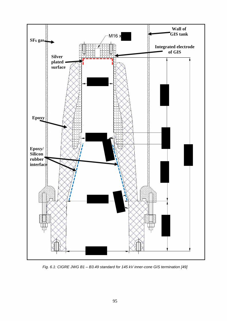
95
Fig. 6.1: CIGRE JWG B1 – B3.49 standard for 145 kV inner-cone GIS termination [49]
Silver
plated
surface
Epoxy
Integrated electrode
of GIS
Wall of
GIS tank
SF6 gas
Epoxy/
Silicon
rubber
interface
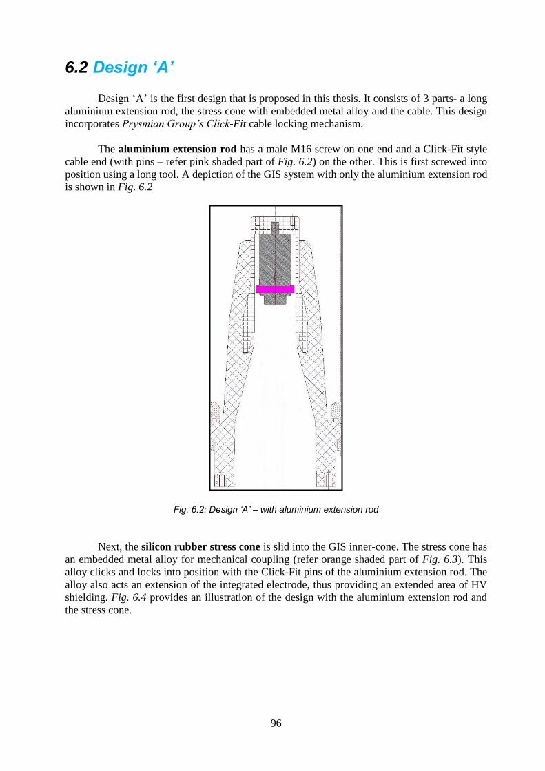
96
6.2 Design ‘A’
Design ‘A’ is the first design that is proposed in this thesis. It consists of 3 parts- a long
aluminium extension rod, the stress cone with embedded metal alloy and the cable. This design
incorporates Prysmian Group’s Click-Fit cable locking mechanism.
The aluminium extension rod has a male M16 screw on one end and a Click-Fit style
cable end (with pins – refer pink shaded part of Fig. 6.2) on the other. This is first screwed into
position using a long tool. A depiction of the GIS system with only the aluminium extension rod
is shown in Fig. 6.2
Fig. 6.2: Design ‘A’ – with aluminium extension rod
Next, the silicon rubber stress cone is slid into the GIS inner-cone. The stress cone has
an embedded metal alloy for mechanical coupling (refer orange shaded part of Fig. 6.3). This
alloy clicks and locks into position with the Click-Fit pins of the aluminium extension rod. The
alloy also acts an extension of the integrated electrode, thus providing an extended area of HV
shielding. Fig. 6.4 provides an illustration of the design with the aluminium extension rod and
the stress cone.
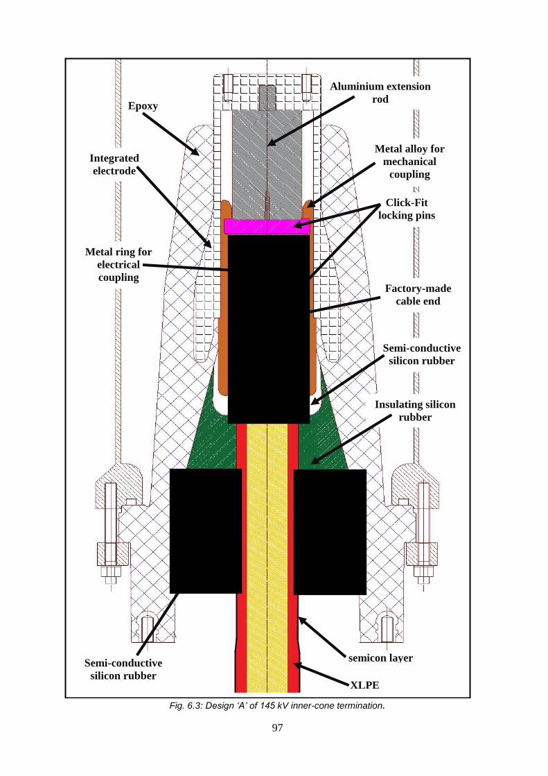
97
Fig. 6.3: Design ‘A’ of 145 kV inner-cone termination.
Aluminium extension
rod
Metal alloy for
mechanical
coupling
Click-Fit
locking pins
Semi-conductive
silicon rubber
Insulating silicon
rubber
Epoxy
Integrated
electrode
Factory-made
cable end
XLPE
Semi-conductive
silicon rubber
Metal ring for
electrical
coupling
semicon layer

98
Fig. 6.4: Design ‘A’ – with aluminium extension rod and stress cone.
The factory-made cable end is then plugged into the stress cone (similar to the
assembling of pre-moulded joints) until it clicks into the alloy of the stress cone. The necessary
grounding of cable outer sheath is then done.
In order to create and to maintain the interfacial pressure, springs will be required to
provide mechanical pressure. The forces required by the spring is calculated in the following
subsections. Finally, the outer flange is bolted into position. The spring and the outer flange is
not shown in Fig. 6.3, as the focus of this thesis is on the design of the silicon rubber insulator.
A complete illustration of this design is shown in Fig. 6.3.
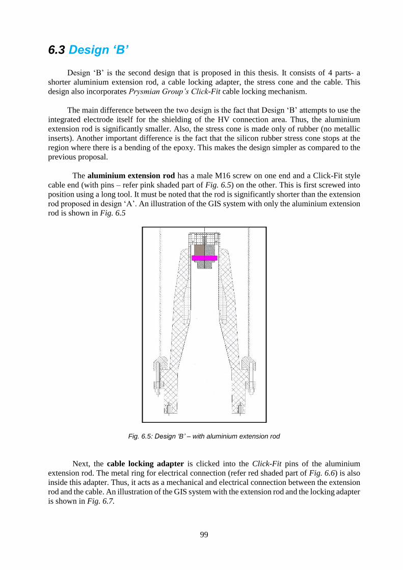
99
6.3 Design ‘B’
Design ‘B’ is the second design that is proposed in this thesis. It consists of 4 parts- a
shorter aluminium extension rod, a cable locking adapter, the stress cone and the cable. This
design also incorporates Prysmian Group’s Click-Fit cable locking mechanism.
The main difference between the two design is the fact that Design ‘B’ attempts to use the
integrated electrode itself for the shielding of the HV connection area. Thus, the aluminium
extension rod is significantly smaller. Also, the stress cone is made only of rubber (no metallic
inserts). Another important difference is the fact that the silicon rubber stress cone stops at the
region where there is a bending of the epoxy. This makes the design simpler as compared to the
previous proposal.
The aluminium extension rod has a male M16 screw on one end and a Click-Fit style
cable end (with pins – refer pink shaded part of Fig. 6.5) on the other. This is first screwed into
position using a long tool. It must be noted that the rod is significantly shorter than the extension
rod proposed in design ‘A’. An illustration of the GIS system with only the aluminium extension
rod is shown in Fig. 6.5
Fig. 6.5: Design ‘B’ – with aluminium extension rod
Next, the cable locking adapter is clicked into the Click-Fit pins of the aluminium
extension rod. The metal ring for electrical connection (refer red shaded part of Fig. 6.6) is also
inside this adapter. Thus, it acts as a mechanical and electrical connection between the extension
rod and the cable. An illustration of the GIS system with the extension rod and the locking adapter
is shown in Fig. 6.7.
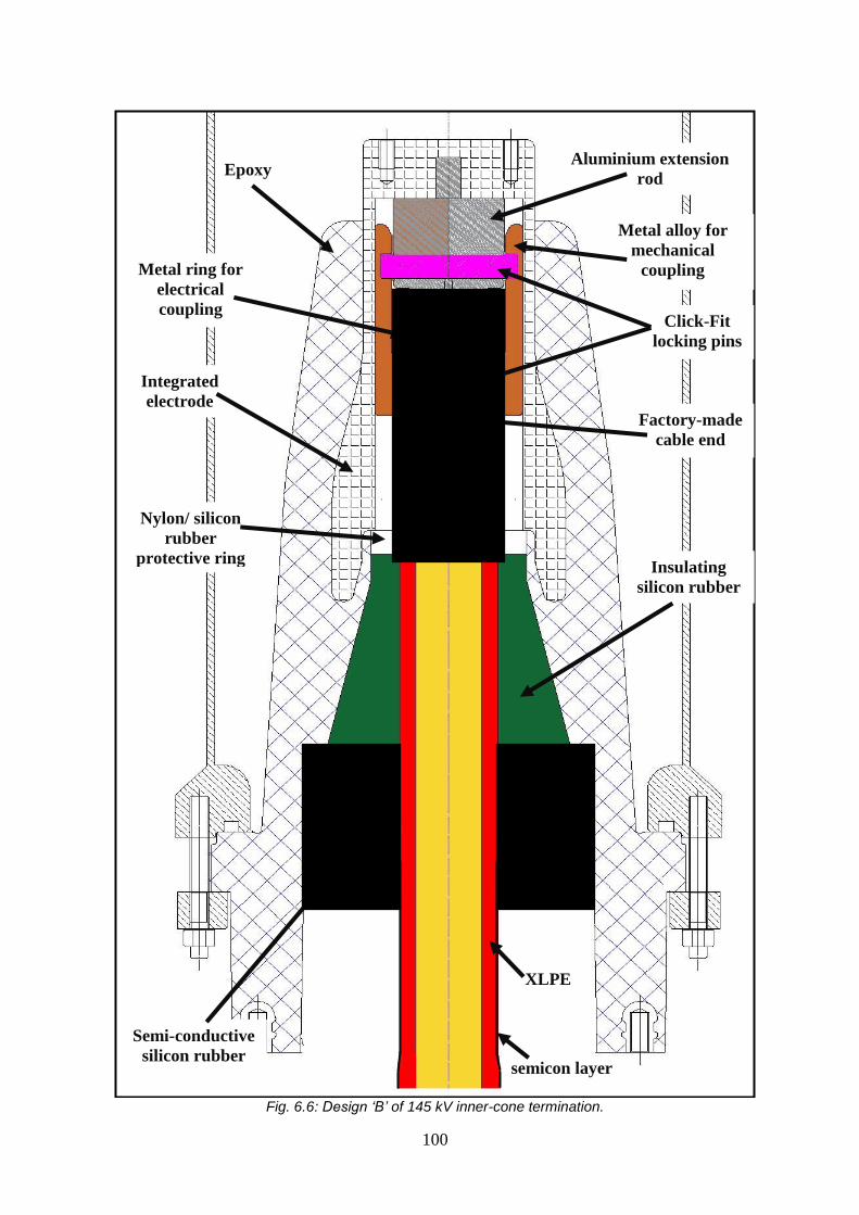
100
Fig. 6.6: Design ‘B’ of 145 kV inner-cone termination.
Aluminium extension
rod
Metal alloy for
mechanical
coupling
Click-Fit
locking pins
Nylon/ silicon
rubber
protective ring Insulating
silicon rubber
Epoxy
Factory-made
cable end
semicon layer
Semi-conductive
silicon rubber
Metal ring for
electrical
coupling
Integrated
electrode
XLPE
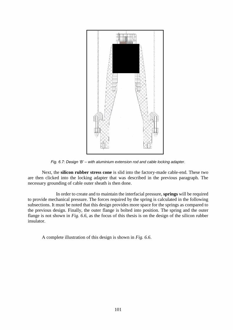
101
Fig. 6.7: Design ‘B’ – with aluminium extension rod and cable locking adapter.
Next, the silicon rubber stress cone is slid into the factory-made cable-end. These two
are then clicked into the locking adapter that was described in the previous paragraph. The
necessary grounding of cable outer sheath is then done.
In order to create and to maintain the interfacial pressure, springs will be required
to provide mechanical pressure. The forces required by the spring is calculated in the following
subsections. It must be noted that this design provides more space for the springs as compared to
the previous design. Finally, the outer flange is bolted into position. The spring and the outer
flange is not shown in Fig. 6.6, as the focus of this thesis is on the design of the silicon rubber
insulator.
A complete illustration of this design is shown in Fig. 6.6.
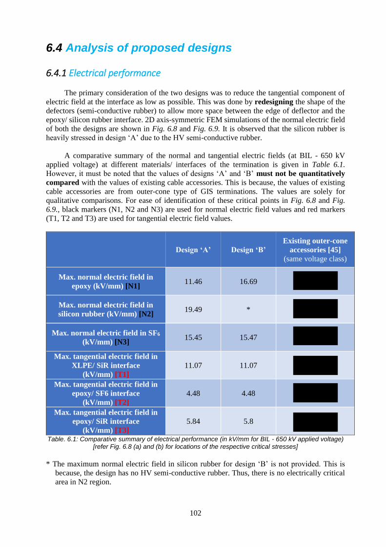
102
6.4 Analysis of proposed designs
6.4.1 Electrical performance
The primary consideration of the two designs was to reduce the tangential component of
electric field at the interface as low as possible. This was done by redesigning the shape of the
defectors (semi-conductive rubber) to allow more space between the edge of deflector and the
epoxy/ silicon rubber interface. 2D axis-symmetric FEM simulations of the normal electric field
of both the designs are shown in Fig. 6.8 and Fig. 6.9. It is observed that the silicon rubber is
heavily stressed in design ‘A’ due to the HV semi-conductive rubber.
A comparative summary of the normal and tangential electric fields (at BIL - 650 kV
applied voltage) at different materials/ interfaces of the termination is given in Table 6.1.
However, it must be noted that the values of designs ‘A’ and ‘B’ must not be quantitatively
compared with the values of existing cable accessories. This is because, the values of existing
cable accessories are from outer-cone type of GIS terminations. The values are solely for
qualitative comparisons. For ease of identification of these critical points in Fig. 6.8 and Fig.
6.9., black markers (N1, N2 and N3) are used for normal electric field values and red markers
(T1, T2 and T3) are used for tangential electric field values.
Design ‘A’ Design ‘B’
Existing outer-cone
accessories [45]
(same voltage class)
Max. normal electric field in
epoxy (kV/mm) [N1] 11.46 16.69
Max. normal electric field in
silicon rubber (kV/mm) [N2] 19.49 *
Max. normal electric field in SF6
(kV/mm) [N3] 15.45 15.47
Max. tangential electric field in
XLPE/ SiR interface
(kV/mm) [T1]
11.07 11.07
Max. tangential electric field in
epoxy/ SF6 interface
(kV/mm) [T2]
4.48 4.48
Max. tangential electric field in
epoxy/ SiR interface
(kV/mm) [T3]
5.84 5.8
Table. 6.1: Comparative summary of electrical performance (in kV/mm for BIL - 650 kV applied voltage) [refer Fig. 6.8 (a) and (b) for locations of the respective critical stresses]
* The maximum normal electric field in silicon rubber for design ‘B’ is not provided. This is
because, the design has no HV semi-conductive rubber. Thus, there is no electrically critical
area in N2 region.

103
Fig. 6.8 (a): Design ‘A’ – Normal electric field in kV/mm at 650 kV (BIL).
Fig. 6.8 (b): Design ‘B’ – Normal electric field in kV/mm at 650 kV (BIL).
N1 - Max. normal electric field in epoxy; T1 - Max. tangential electric field in XLPE/ SiR interface N2 - Max. normal electric field in silicon rubber; T2 - Max. tangential electric field in epoxy/ SF6 interface N3 - Max. normal electric field in SF6; T3 - Max. tangential electric field in epoxy/ SiR interface
T2
T1
T3
N3
N1
N2
N1
N3
T1
T3
T2
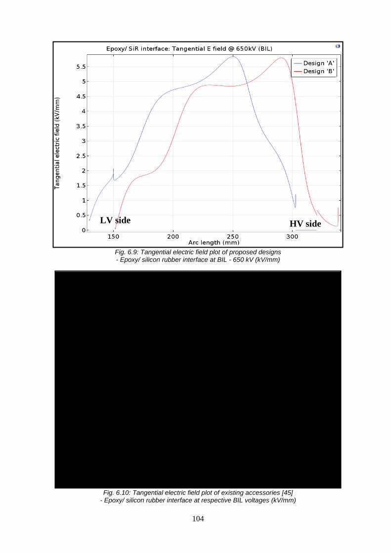
104
Fig. 6.9: Tangential electric field plot of proposed designs - Epoxy/ silicon rubber interface at BIL - 650 kV (kV/mm)
Fig. 6.10: Tangential electric field plot of existing accessories [45]
- Epoxy/ silicon rubber interface at respective BIL voltages (kV/mm)
HV side LV side
HV side LV side
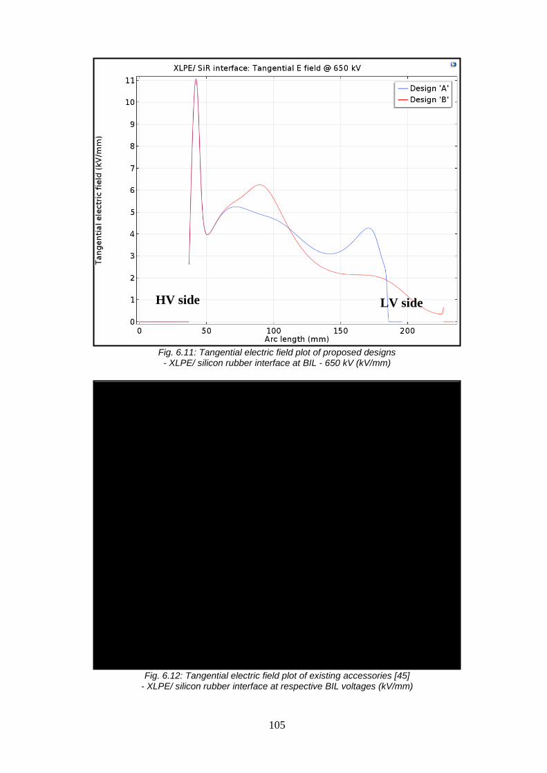
105
Fig. 6.11: Tangential electric field plot of proposed designs
- XLPE/ silicon rubber interface at BIL - 650 kV (kV/mm)
Fig. 6.12: Tangential electric field plot of existing accessories [45]
- XLPE/ silicon rubber interface at respective BIL voltages (kV/mm)
HV side LV side
HV side LV side
106
Fig. 6.13: Tangential electric field plot of proposed designs
- epoxy/ SF6 interface at BIL - 650 kV (kV/mm)
Fig. 6.14: Tangential electric field plot of existing accessories [45]
- epoxy/ SF6 interface at respective BIL voltages (kV/mm)
HV side LV side
HV side LV side

107
Epoxy/ silicon rubber interface
A comparison of the tangential electric field strengths of the epoxy/ silicon rubber interface
of the proposed designs at basic impulse level voltage is shown in Fig. 6.9. Also, a comparative
plot of the tangential electric field values of epoxy/ silicon rubber interfaces of existing cable
accessories at their respective BIL levels is shown in Fig. 6.10. It is clearly observed that both
the proposed designs have a lower tangential electric field component as compared to currently
used outer-cone designs.
From the experimental results discussed in Chapter 5, it was found that for interfacial
pressure of 1 bar, the breakdown occurred at 6 kV/mm. It must be noted that this value is
conservative due to the harsh nature of the test setup, as explained previously. The tangential
electric field values obtained from Fig. 6.9 are less than 6 kV/mm for BIL voltages. Thus, both
the proposed designs will have good/ satisfactory electrical performance of the epoxy/
silicon rubber interface for interfacial pressures greater than 1 bar.
XLPE/ silicon rubber interface
A comparison of the tangential electric field strengths of the XLPE/ silicon rubber interface
of the two proposed designs [maximum value 11.07 kV/mm] at basic impulse level voltage is
shown in Fig. 6.11. Also, a comparative plot of the tangential electric field values of XLPE/
silicon rubber interfaces of existing cable accessories [maximum value X kV/mm] at their
respective BIL levels is shown in Fig. 6.12. It is clearly observed that both the proposed designs
have a lower tangential electric field component as compared to currently used outer-cone
designs.
Epoxy/ SF6 interface
A comparison of the tangential electric field strengths of the epoxy/ SF6 interface of the
two proposed designs [maximum value 4.48 kV/mm] at basic impulse level voltage is shown in
Fig. 6.13. Also, a comparative plot of the tangential electric field values of epoxy/ SF6 interfaces
of existing cable accessories [maximum value X kV/mm] at their respective BIL levels is shown
in Fig. 6.14. It is clearly observed that both the proposed designs have a lower tangential
electric field component as compared to currently used outer-cone designs.
Based on calculations and the experimental findings, it is evident that both the
proposed designs have better electrical performance than the currently used outer-cone
GIS cable terminations.
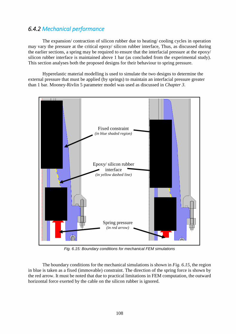
108
6.4.2 Mechanical performance
The expansion/ contraction of silicon rubber due to heating/ cooling cycles in operation
may vary the pressure at the critical epoxy/ silicon rubber interface, Thus, as discussed during
the earlier sections, a spring may be required to ensure that the interfacial pressure at the epoxy/
silicon rubber interface is maintained above 1 bar (as concluded from the experimental study).
This section analyses both the proposed designs for their behaviour to spring pressure.
Hyperelastic material modelling is used to simulate the two designs to determine the
external pressure that must be applied (by springs) to maintain an interfacial pressure greater
than 1 bar. Mooney-Rivlin 5 parameter model was used as discussed in Chapter 3.
Fig. 6.15: Boundary conditions for mechanical FEM simulations
The boundary conditions for the mechanical simulations is shown in Fig. 6.15, the region
in blue is taken as a fixed (immovable) constraint. The direction of the spring force is shown by
the red arrow. It must be noted that due to practical limitations in FEM computation, the outward
horizontal force exerted by the cable on the silicon rubber is ignored.
Fixed constraint (in blue shaded region)
Spring pressure (in red arrow)
Epoxy/ silicon rubber
interface (in yellow dashed line)

109
Fig. 6.16: Design ‘A’- plot of pressure distribution (in bar) for a spring force
(shown by red arrow) of 5 bar
Fig. 6.17: Design ‘B’- plot of pressure distribution (in bar) for a spring force
(shown by red arrow) of 5 bar
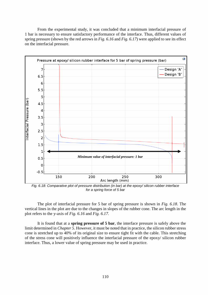
110
From the experimental study, it was concluded that a minimum interfacial pressure of
1 bar is necessary to ensure satisfactory performance of the interface. Thus, different values of
spring pressure (shown by the red arrows in Fig. 6.16 and Fig. 6.17) were applied to see its effect
on the interfacial pressure.
Fig. 6.18: Comparative plot of pressure distribution (in bar) at the epoxy/ silicon rubber interface
for a spring force of 5 bar
The plot of interfacial pressure for 5 bar of spring pressure is shown in Fig. 6.18. The
vertical lines in the plot are due to the changes in slopes of the rubber cone. The arc length in the
plot refers to the y-axis of Fig. 6.16 and Fig. 6.17.
It is found that at a spring pressure of 5 bar, the interface pressure is safely above the
limit determined in Chapter 5. However, it must be noted that in practice, the silicon rubber stress
cone is stretched up to 40% of its original size to ensure tight fit with the cable. This stretching
of the stress cone will positively influence the interfacial pressure of the epoxy/ silicon rubber
interface. Thus, a lower value of spring pressure may be used in practice.
Minimum value of interfacial pressure: 1 bar
111
6.5 Summary
It is observed that both the proposed designs would need a spring in the bottom (shown
by the red arrow in Fig. 6.15). The spring would ensure that the interfacial pressure at the critical
epoxy/ silicon rubber interface is maintained above 1 bar, during its operational cycles.
Design ‘B’ is more suitable from a product perspective. This is because of its simpler
design (no embedded metal), which would result in ease of manufacture and lower production
costs.
The modularity offered by this standardisation in combination with the ease and lower
installation cost/ time would be an USP for this type of products.
This product is of significance due to the upcoming refurbishment of the 145 kV grids
by TSOs in the EU. Owing to this commercial aspect, these types of terminations are expected
to be commercially available soon. These standardised designs have the following unique
advantages:
1. They are a new standardisation, which means that all accessories manufacturers will soon
showcase their standardised designs. This would promote healthy competition and
possible further development of this technology for other voltage classes.
2. The flexibility (modularity) given to the GIS manufacturer by the standardised interface
would enable them to test the entire GIS switchgear with the epoxy at once.
3. The insulator is independent of the cable manufacturer. This standardisation would allow
the utilities to plan GIS projects without considering the cable manufacturer, as the cable
part can be dealt with, in the later stages of the project.

112
113
7. Conclusions and future scope
This chapter summarises the conclusions from the various experiments and FEM calculations
performed during the course of this thesis work. It also gives answers to the research goals of
this work. Recommendations for future research are also stated.
114
7.1 Conclusions
The final objective of this M.Sc. thesis is to propose the design for a new 145 kV
inner-cone GIS termination in accordance to CIGRE JWG B1-B3.49 recommendations. This new
(design) technology required a detailed study of the epoxy/ silicon rubber interface. Which in
turn required the design of a new test setup for interfacial testing. All these objectives have been
successfully achieved. A summary of the conclusions from different sections of this work are
presented below:
Modelling of silicon rubber:
1. It was found that a new type of material modelling technique (hyperelastic material
modelling) must be used to accurately model the behaviour of the silicon rubber.
2. Various mechanical tests were performed on the silicon rubber to characterise and deduce
its characteristic modelling technique.
3. It is found that at standard room temperature (23°C) and at elevated temperature (80°C),
the Mooney-Rivlin 5 parameter model provides the best representation of the
mechanical behaviour of the silicon rubber.
Test setup:
4. A new test setup for interfacial testing was designed, built and successfully tested.
5. It is observed that the setup shows very good reproducibility of breakdown values.
6. Due to the design of this test setup, immersion of test setup in oil was not necessary.
7. The AC breakdown voltage and LI voltage limits are determined for the experimental test
setup at standard room temperature. The AC breakdown limit is found to be 50 kV, while
the LI limit is found to be 90 kV.
8. The test setup satisfies all the requirements of the CIGRE 15-10 WG (refer
Section 2.1.1) for interfacial testing of insulation materials.
Experimental testing of epoxy/ silicon rubber interface:
9. It is validated that the electrical performance of the interface improves with increase
in interfacial pressure.
10. The increase in electrical performance of the interface saturates after 1 bar of interfacial
pressure. Thus, this range (1 bar – 2 bar) of interfacial pressure is recommended to be
the interfacial pressure of the epoxy/ silicon rubber interface.
11. It is found that for interfacial pressure of 1 bar, the interface has a breakdown strength of
6 kV/mm at standard room temperature. This is a conservative value.
115
12. It is found that the presence of silicon grease, increases the electrical strength of the
interface by at least 40 %.
13. A scratch on the epoxy surface can reduce the electrical performance of the interface by
up to 11 %. This is equivalent to a 0.5 bar decrease in interfacial pressure.
14. It is found that heated samples (testing at elevated temperature of 85 - 90°C) reduces the
electrical performance of the interface as compared to the results obtained from the AC
breakdown tests.
15. It is concluded that the interface can withstand at least 90 kV of LI voltage for 1 bar of
interfacial pressure (at standard room temperature).
Design of 145 kV inner-cone GIS cable termination:
16. Two designs are proposed adhering to the design limitations as laid down by the
CIGRE JWG B1 – B3.49 JWG.
17. Both the designs use an aluminium extension rod (of different lengths) to connect with
the M16 bolt of the GIS.
18. The Click-Fit locking concept is retained in both the designs. This aligns the new
inner-cone termination with all existing Click-Fit cable accessories of Prysmian Group.
19. Design ‘A’ has a silicon rubber stress cone with an embedded metal alloy for mechanical
connection. This stress cone contains the mechanical and electrical connection regions.
20. Design ‘B’ has a silicon rubber stress cone purely for field control of the cable end. The
electrical and mechanical connection with the GIS is made through a separate connector
and the aluminium extension rod. This design is simpler because it has no embedded
metal alloy.
21. A spring is necessary to ensure sufficient interfacial pressure of the epoxy/ silicon rubber
interface. About 5 bar of spring force is required.

116
7.2 Answers to research goals/ questions
In order to fulfil the academic requirements of a Master of Science thesis, certain scientific
research goals need to be achieved. All the research goals planned at the start of this thesis have
been successfully achieved.
Goal 1: To design a test setup to obtain the relation between electric field strength with respect
to interfacial pressure
A new modular test setup has been successfully designed, built and tested. The test
setup satisfies all the requirements of the CIGRE 15-10 WG.
Goal 2: To experimentally obtain the relation between interfacial pressure and electric
performance of epoxy/ silicon rubber interface.
AC breakdown tests were carried out for a wide range (0.2 bar – 2 bar) of interfacial
pressures. The values of interfacial pressures showed very low scatter/ dispersion. Thus,
the remaining samples were used for additional tests to further characterise the interface
behaviour.
Additional tests:
AC breakdown test with silicon grease at the interface
AC breakdown test with scratch on epoxy surface
AC breakdown test at elevated temperature
Lightning Impulse (LI) test
The additional tests helped to provide a better and more complete understanding of the
interfacial electrical behaviour.
Goal 3: To propose a design for an inner-cone GIS cable termination and elucidate its
electrical and mechanical features.
Two new designs of the new 145 kV inner-cone GIS cable termination have been
proposed. Comparison of the electrical and mechanical characteristics of both the
designs has been performed. A comparison of critical electrical parameters with those
of existing cable accessories has been also performed.
Apart from these goals, the following additional finding has also been made during this thesis:
A new material modelling technique for insulating silicon rubber has been studied in
detail. Extensive mechanical tests were performed to characterise and validate the
material model of silicon rubber. This will help to understand the behaviour of silicon
rubber in existing/ future designs of cable accessories.
The performance of the test setup has been extremely stable and shows very low standard
deviation. Thus, the design of this test setup will be shared with the larger scientific
community through an IEEE publication.
117
7.3 Recommendations for future work
The following recommendations are made for further study in this domain:
1. Due to lack of standardised method for testing interfaces, it is not possible to compare
and collaborate the works of different authors/ institutes. Thus, relevant bodies must
device standardised procedures and test setups for interfacial testing.
2. The proposed test setup in this thesis may be modified/ adapted to perform tan δ, leakage
current and partial discharge measurements
3. A study for mathematical/ theoretical breakdown performance of interfaces (using
interface models) and validation by experimental results could be performed.
4. In accordance with the trend of the cable industry, the behaviour of interfaces under DC
and low frequency AC voltage should also be explored.
5. For the hyperelastic modelling of silicon rubber, further tests like biaxial, shear and
volumetric could be performed. These tests will give a better accuracy and understanding
of the hyperelastic material model of the rubber.

118
119
Bibliography [1.] A. Rodrigo Mor. ET8020. Class Lecture, Topic: “Diagnostics of High Voltage and Asset
Management”. Faculty of Electrical Engineering, Mathematics and Computer Science,
TU Delft, The Netherlands, June 2017.
[2.] A.N..Gent. Engineering with Rubber - How to Design Rubber Components.
ISBN 978-3446427648.
[3.] ANSYS Inc. Ansys theory reference 5.6.
URL http://research.me.udel.edu/~lwang/teaching/MEx81/ansys56manual.pdf.
[4.] Standard Test Method for Dielectric Breakdown Voltage and Dielectric Strength of Solid
Electrical Insulating Materials at Commercial Power Frequencies, ASTM D149-09,
(2013).
[5.] B. Du and L. Gu. "Effects of interfacial pressure on tracking failure between XLPE and
silicon rubber". IEEE Transactions on Dielectrics and Electrical Insulation, vol. 17, no. 6,
pp. 1922-1930, 2010.
[6.] B. Parmigiani. Accessories for underground and submarine cable systems. Italy: Prysmian
S.P.A.„ 2013.
[7.] C. Forssen and A. Christerson. "Test cell for interfacial electric strength testing". IEEE
International Conference on Solid Dielectrics (ICSD), 2013.
[8.] C. Forssen, A. Christerson and D. Borg. "Test cell for electric strength of rubber-epoxy
interfaces". 2015 IEEE Conference on Electrical Insulation and Dielectric Phenomena
(CEIDP), 2015.
[9.] C. Zhang, J. Kucera and R. Kaluzny. "The Electrical Behaviours of the Interface in Solid-
Insulated Distribution Equipment". 2008 Annual Report Conference on Electrical
Insulation and Dielectric Phenomena, 2008.
[10.] COMSOL AB. “Introduction to COMSOL Multiphysics”.
Internet: http://www-cs-faculty.stanford.edu/~uno/abcde.html [November 8, 2017].
[11.] D. Bortoli, E. Wrubleski, R.J. Marczak and J.G. Junior . "Hyperfit - curve fitting software
for incompressible hyperelastic material models". Brazilian Congress of Mechanical
Engineering, 2011.
[12.] D. Fournier and L. Lamarre. "Effect of Pressure and Length on Interfacial Breakdown
Between Two Dielectric Surfaces". IEEE International Symposium on Electrical
Insulation, Baltimore, MD USA, pp. 270-272, 1992.
[13.] D. Fournier and L. Lamarre. "Effect of pressure and temperature on interfacial breakdown
between two dielectric surfaces". Proc. 1992 Annual Report: Conference on Electrical
Insulation and Dielectric Phenomena, Victoria, B.C., pp. 229-235, 1992.
[14.] D. Panagiotopoulos. "AC Electrical Breakdown Strength of Solid Solid Interfaces: A study
about the effect of elasticity, pressure and interface conditions.", M.Sc. thesis. Norwegian
University of Science and Technology, Norway, 2015.
[15.] D. Roylance. “Stress Strain Curves”. Internet:
http://web.mit.edu/course/3/3.11/www/modules/ss.pdf , August 23, 2001 [January 26,
2018].
[16.] E. Kantar, D. Panagiotopoulos and E. Ildstad. "Factors influencing the tangential AC
breakdown strength of solid-solid interfaces". IEEE Electrical Insulation Magazine, vol.
23, no. 3, pp. 1778-1788, 2016.
120
[17.] E. Kantar and E. Ildstad. “Modelling Longitudinal Breakdown Strength of Solid – Solid
Interfaces using Contact Theory”. 2016 IEEE International Conference on Dielectrics, vol.
1, pp. 398 – 401, July 2016.
[18.] E. Kantar, F. Mauseth and E. Ildstad. “Effect of Pressure and Elastic Modulus on
Tangential Breakdown Strength of Solid – Solid Interfaces”. IEEE Electrical Insulation
Conference, Montreal, Canada, pp. 431 – 435, June 2016.
[19.] F. H. Kreuger. Industrial High Voltage Vol. I. Delft University Press, 1991.
ISBN 978-9062755615.
[20.] F. H. Kreuger. Industrial High Voltage Vol. II. Delft University Press, 1992.
ISBN 978-9062755622.
[21.] Feasibility of a common dry type plug-in interface for GIS and power cables above 52kV,
CIGRE JWG B1-B3.33.
[22.] H. Lobo and B. Croop. “Testing, modelling and validation for rubber simulation in
ANSYS”. Internet:
http://engr.bd.psu.edu/ansysug/2016-10-1/2DPLworkshopOct2016_HyperWorking.pdf.
[December 22, 2017]
[23.] High-voltage switchgear and control gear - Part 209: Cable connections for gas insulated
metal-enclosed switchgear for rated voltages above 52kV - Fluid-filled and extruded
insulation cables - Fluid-filled and dry-type cable-terminations, IEC 62271-209:2007-08.
[24.] High-voltage test techniques – Part 1: general definitions and test requirements,
IEC 60060-1:2010.
[25.] IEC/IEEE Guide for the Statistical Analysis of Electrical Insulation Breakdown Data
(Adoption of IEEE Std. 930-2004), IEEE Standard 62539, 2007.
[26.] Insulation coordination – Part 1: Definitions, principles and rules, IEC 60071-1:2006.
[27.] Interfaces in accessories for extruded HV and EHV cables, CIGRE Joint Task Force
21/15(210), August 2002.
[28.] J. Andersson, S. Gubanski and H.Hillborg. "Properties of interfaces between silicone
rubber and epoxy". IEEE Electrical Insulation Magazine, vol. 15, no. 5, pp. 1360-1367,
2008.
[29.] J. Svahn. L. Hedman and S.M. Gubanski. "Development of Cell for Testing of the
Interfacial Electric Strength". CIGRE WG15-10, 1998.
[30.] J. T. Bauman. Fatigue, Stress and Strain of Rubber Components - Guide for Design
Engineers. ISBN 978-3446416819.
[31.] M. Sasso, G. Palmieri, G. Chiappini and D. Amodio. "Characterization of hyperelastic
rubber-like materials by biaxial and uniaxial stretching tests based on optical methods".
Elsevier - Polymer Testing, vol. 27, pp. 994-1004, 2008.
[32.] M.Z. Siddiqui M. Shahzad, A. Kamran and M. Farhan. Mechanical characterization and
finite element modelling of a hyperelastic material. 18, 2015.
[33.] NPTEL. “Mechanical properties of materials”. Internet:
http://nptel.ac.in/courses/107103012/module1/lec4.pdf [February 14, 2018]
[34.] Oil immersed cable connection assemblies for transformers and reactors having highest
voltage for equipment Um from 72.5kV to 550kV - Part 2: Dry-type cable terminations,
NEN-EN 50299-2.
[35.] Pfisterer Kontaktsysteme GmbH. “High Voltage Cable Plug”. US Patent 2016/ 0352036,
Dec 1, 2016.
[36.] P.T.M. Vaessen. ET4103. Class Lecture, Topic: “High Voltage Constructions”. Faculty of
Electrical Engineering, Mathematics and Computer Science, TU Delft, The Netherlands,
February 2017.
121
[37.] Power Cables with extruded insulation and their accessories for rated voltages above 30
kV (Um = 36 kV) up to 150 kV (Um= 170 kV) – Test methods and requirements,
IEC 60840:2011.
[38.] Prysmian Group. “Click-Fit”. URL: http://www.click-fit.org/ [April 12, 2018].
[39.] R. Jakel. “Analysis of hyperelastic materials with mechanica - theory and application
examples”. Internet:
http://qucosa.de/fileadmin/data/qucosa/documents/5995/data/Analysis_of_Hyperelastic_
Materials_with_MECHANICA.pdf. [February 2, 2018].
[40.] R. Ross. "Dealing with interface problems in polymer cable terminations". IEEE Electrical
Insulation Magazine, vol. 15, no. 4, pp. 5-9, 1999.
[41.] R.W. Ogden, G. Saccomandi and I. Sgura. "Fitting hyperelastic models to experimental
data". Springer – Computational Mechanics, 2004.
[42.] Rubber, vulcanised or thermoplastic -Determination of tensile stress-strain properties,
NEN-ISO 37: 2017.
[43.] Rubber vulcanized or thermoplastic - Determination of compression set - Part 1: At
ambient or elevated temperatures, NEN-ISO 815-1:2008.
[44.] S. Ganeshan, J. Murugesan, A. Cavallini, F. Negri, B. Valecillos and U. Piovan.
"Identification of partial discharges in power transformers: An approach driven by practical
experience". IEEE Electrical Insulation Magazine, vol. 33, no. 5, pp. 23-31, 2017.
[45.] S. Ganeshan, “Electrical analysis of power cable accessories” Internship report, TU Delft,
The Netherlands, 2017.
[46.] S. Hasheminezhad, E. Ildstad and A. Nysveen. "Breakdown strength of solid - solid
interface". IEEE International Conference on Solid Dielectrics, 2010.
[47.] S. Hasheminezhad. "Breakdown strength of solid | solid interfaces". IEEE Trondheim
PowerTech, 2011.
[48.] S. Rowland. “Position Paper on Interfaces in Solid Dielectric Insulation Systems”. URL:
http://www.hubnet.org.uk/filebyid/634/Solid_Dielectrics.pdf [November 9, 2017].
[49.] Standard design of a common, dry type plug-in interface for GIS and power cables up to
145kV, CIGRE WG B1-B3.49. [March 20, 2018]
[50.] Standard Test Methods for Rubber Properties in Compression, ASTM D575 - 91(2012).
[51.] T. Sussman and K.J. Bathe. "A model of incompressible isotropic hyperelastic material
behaviour using spline interpolations of tension-compression data". Wiley InterScience -
Communications in Numerical Methods in Engineering, vol. 25, pp. 53-63, 2008.
[52.] T. Takahashi, T. Okamoto, Y. Ohki and K. Shibata. "Breakdown strength at the interface
between epoxy resin and silicone rubber - A basic study for the development of all solid
insulation". IEEE Electrical Insulation Magazine, vol. 12, no. 4, pp. 719-724, 2005.
[53.] T. Tanaka. "Polymer Interfaces Associated with Electric Insulation Systems". CIGRE SC
15 colloquium, Bedford, Mass., USA, 1997.
[54.] University of Colorado- Boulder. “Ch. 5 Stress- strain material laws”. [On-line].
Available:
https://www.colorado.edu/engineering/CAS/courses.d/Structures.d/IAST.Lect05.d/IAST.
Lect05.pdf [February 2, 2018]

122