msp430™ 32-khz crystal oscillators - ti.com
TRANSCRIPT

1SLAA322D–August 2006–Revised July 2017Submit Documentation Feedback
Copyright © 2006–2017, Texas Instruments Incorporated
MSP430™ 32-kHz Crystal Oscillators
Application ReportSLAA322D–August 2006–Revised July 2017
MSP430™ 32-kHz Crystal Oscillators
Peter Spevak and Peter Forstner............................................................................ MSP430 Applications
ABSTRACTSelection of the right crystal, correct load circuit, and proper board layout are important for a stable crystaloscillator. This application report summarizes crystal oscillator function and explains the parameters toselect the correct crystal for ultra-low-power operation of an MSP430™ MCU. In addition, hints andexamples for correct board layout are given. The document also contains detailed information on thepossible oscillator tests to ensure stable oscillator operation in mass production.
For additional information about the factors that influence the accuracy of the low-frequency oscillator, seeMSP430™ LFXT1 Oscillator Accuracy.
Contents1 The 32-kHz Crystal Oscillator .............................................................................................. 2
1.1 The Crystal .......................................................................................................... 21.2 The Oscillator........................................................................................................ 3
2 Crystal Selection ............................................................................................................. 42.1 Effective Load Capacitance ....................................................................................... 42.2 ESR Value ........................................................................................................... 52.3 Tolerance ............................................................................................................ 62.4 Start-up Time ........................................................................................................ 7
3 PCB Design Considerations................................................................................................ 84 Testing the Crystal Oscillator ............................................................................................. 10
4.1 Oscillator Frequency vs Load Capacitance .................................................................... 104.2 Negative Resistance Method .................................................................................... 104.3 Relationship Between Crystal ESR and Safety Factor ....................................................... 11
5 Crystal Oscillator in Production........................................................................................... 125.1 PCB Material, Quality, and Cleaning ........................................................................... 125.2 Soldering and Contact Impedance.............................................................................. 135.3 Environmental Influences, Temperature, and Humidity ...................................................... 135.4 Device-Specific Features to Support Better Start-up Behavior.............................................. 14
6 Hardware Troubleshoot for Crystal-Oscillator Start-up in Production ............................................... 187 References .................................................................................................................. 20
List of Figures
1 Mechanical Oscillation of a Tuning-Fork Crystal ........................................................................ 22 Equivalent Circuit of a Crystal.............................................................................................. 33 Reactance of a Crystal...................................................................................................... 34 Principle Pierce Oscillator Circuit .......................................................................................... 45 Frequency vs Load Capacitance for a 0-ppm Crystal .................................................................. 56 Frequency Deviation of a Tuning-Fork Crystal Over Temperature.................................................... 67 Layout Without and With External Load Capacitors (XIN and XOUT Neighboring Pins Are Standard
Function Pins) ................................................................................................................ 98 Layout With External Capacitors and Ground Guard Ring (XIN and XOUT Neighboring Pins Are NC
Pins) Examples for MSP430F41x and MSP430F1232IRHB........................................................... 99 Negative Resistance Method With Added Resistor RQ ............................................................... 11

The 32-kHz Crystal Oscillator www.ti.com
2 SLAA322D–August 2006–Revised July 2017Submit Documentation Feedback
Copyright © 2006–2017, Texas Instruments Incorporated
MSP430™ 32-kHz Crystal Oscillators
10 XTS Toggle Assembler Code for an F4xx Device ..................................................................... 1511 Nonoptimized PCB for General Test Purpose.......................................................................... 1612 PCB Optimized for Low-Frequency Oscillator Measurements ....................................................... 1613 LFXT Troubleshooting Decision Tree.................................................................................... 19
List of Tables
1 Typical Oscillation Allowance Values for the 32-kHz Oscillator ....................................................... 62 Safety Factor................................................................................................................ 113 Safety Factor Test Results................................................................................................ 124 Example Coating Materials ............................................................................................... 145 MSP430 MCU Family Overview With Respect to XTS and Corresponding Registers............................ 156 Start-up Time Results Demonstrating the Effect of XTS Toggling Using 42-kΩ Crystal.......................... 177 Start-up Time Results Demonstrating the Effect of XTS Toggling Using 14-kΩ Crystal.......................... 17
TrademarksMSP430 is a trademark of Texas Instruments.3M, Novec are trademarks of 3M.All other trademarks are the property of their respective owners.
1 The 32-kHz Crystal Oscillator
1.1 The CrystalFor an ultra-low-power design, only low-frequency crystals are usable, because with higher-frequencyoscillators, the current consumption increases significantly. Tuning-fork crystals typically have a frequencyrange of 10 kHz to 200 kHz in fundamental mode and a maximum drive level of 1 µW. These parametersmake them the first choice for the 32768-Hz ultra-low-power crystal oscillator in MSP430 microcontrollers.
Every MSP430 MCU has a built-in crystal oscillator that can be operated with a tuning-fork crystal at32768 Hz (often called 32 kHz). The mechanical oscillation (see Figure 1) of a 32-kHz tuning fork crystalis converted into an electrical signal. The equivalent electrical circuit of a crystal (see Figure 2) gives theseelectrical characteristics:• CM motional capacitance• LM motional inductance• RM mechanical losses during oscillation• C0 parasitic capacitance of package and pins
Figure 1. Mechanical Oscillation of a Tuning-Fork Crystal

ESR = R 1 +M
C0
CL)2
)
Frequency
FA
FS
Rea
ctan
ce
–jX
+jX
F =A
1 CM
C0
1 +2 L Cπ√ M M
F =S2 L Cπ√ M M
1
CM RM LM
C0
www.ti.com The 32-kHz Crystal Oscillator
3SLAA322D–August 2006–Revised July 2017Submit Documentation Feedback
Copyright © 2006–2017, Texas Instruments Incorporated
MSP430™ 32-kHz Crystal Oscillators
Figure 2. Equivalent Circuit of a Crystal
The series-resonance circuit consisting of CM, LM, and RM represents the electrical equivalent of themechanical resonance of the tuning fork. The frequency characteristics of a crystal's reactance are shownin Figure 3 and give two special frequencies:• FS (series resonance frequency) solely depends on CM and LM and gives a very stable frequency value.
• FA (anti-resonance or parallel-resonance frequency), in addition, also depends on C0, the parasiticcapacitance of package and pins, which is not as precise as the other parameters, CM and LM. Hence,FA gives a less well-defined frequency than FS.
Figure 3. Reactance of a Crystal
The equivalent series resistance (ESR) can be calculated with the formula in Equation 1 from theequivalent circuit in Figure 2:
(1)
C0 is shown in Figure 2 and given by the crystal's data sheet, as is RM or ESR. CL is the required loadcapacitance of a crystal and is also given by the crystal's data sheet.
1.2 The OscillatorThe principle circuit of an oscillator is shown in Figure 4. Two basic parameters must be fulfilled to enableoscillation:• Closed loop gain ≥ 1 for oscillator start up and
closed loop gain = 1 for stable oscillation• Closed loop phase shift = n × 360°

C =Load
C + CL1 Parasitic
2
C =Load
C' × C'L1 L2
C' + C'L1 L2
Loop Gain = 1360°
180°
Amplifier
CL1 CL2
180°
Crystal Selection www.ti.com
4 SLAA322D–August 2006–Revised July 2017Submit Documentation Feedback
Copyright © 2006–2017, Texas Instruments Incorporated
MSP430™ 32-kHz Crystal Oscillators
Figure 4. Principle Pierce Oscillator Circuit
Figure 4 shows the Pierce oscillator circuit, which takes advantage of the crystal's serial resonancefrequency. The inverting amplifier gives a phase shift of approximately 180°. The feedback circuitconsisting of a 32-kHz crystal and two load capacitors adds another 180° phase shift. This results in therequired oscillator closed-loop phase shift of 360°. The closed-loop gain must be adjusted with the gain ofthe inverting amplifier. All MSP430 32-kHz crystal oscillators are Pierce oscillators.
2 Crystal SelectionThe most important parameters when choosing a crystal are:• Crystal's required effective load capacitance (for 32-kHz crystals, typically 6 pF to 15 pF)• Crystal's ESR (for 32-kHz crystals, typically 30 kΩ to 100 kΩ)• Tolerance (typically 5 ppm to 30 ppm)
All of these crystal parameters are given by the crystal data sheet but can be also measured at the realcrystal using, for example, crystal impedance bridge, a vector voltmeter, or a network analyzer. It is veryimportant to know these parameters, because otherwise it is not possible to design a stable oscillator.
2.1 Effective Load CapacitanceThe Pierce oscillator (see Figure 4) uses two load capacitors, CL1 and CL2, as load for the crystal. Thesecapacitors generate, together with the crystal's inductance (LM) (see Figure 2), the required 180° phaseshift of the feedback loop. From the view of the crystal, these capacitors are a serial connection throughGND. Hence, if using two equal capacitors, the values of these capacitors must be twice the required loadcapacitance. It is also important to consider all parasitic capacitances, such as PCB traces and MSP430MCU pin capacitance, for the calculation of the necessary capacitors according to Equation 2.
(2)
Where:C'L1 = CL1 + CL1Parasitic
C'L2 = CL2 + CL2Parasitic
When using equal capacitors for CL1 and CL2 and a symmetric layout with equal parasitic capacitance onboth crystal pins, the effective load capacitance is shown in Equation 3.
(3)
Example:
32760 Hz
32762 Hz
32764 Hz
32766 Hz
32768 Hz
32770 Hz
32772 Hz
32774 Hz
32776 Hz
32778 Hz
32780 Hz
1 pF 3 pF 5 pF 7 pF 9 pF 11 pF 13 pF 15 pF 17 pF 19 pF
Load Capacitance
Freq
uenc
y
Crystal FrequencyC DependentL Effective Load
Capacitance
Frequency Target
www.ti.com Crystal Selection
5SLAA322D–August 2006–Revised July 2017Submit Documentation Feedback
Copyright © 2006–2017, Texas Instruments Incorporated
MSP430™ 32-kHz Crystal Oscillators
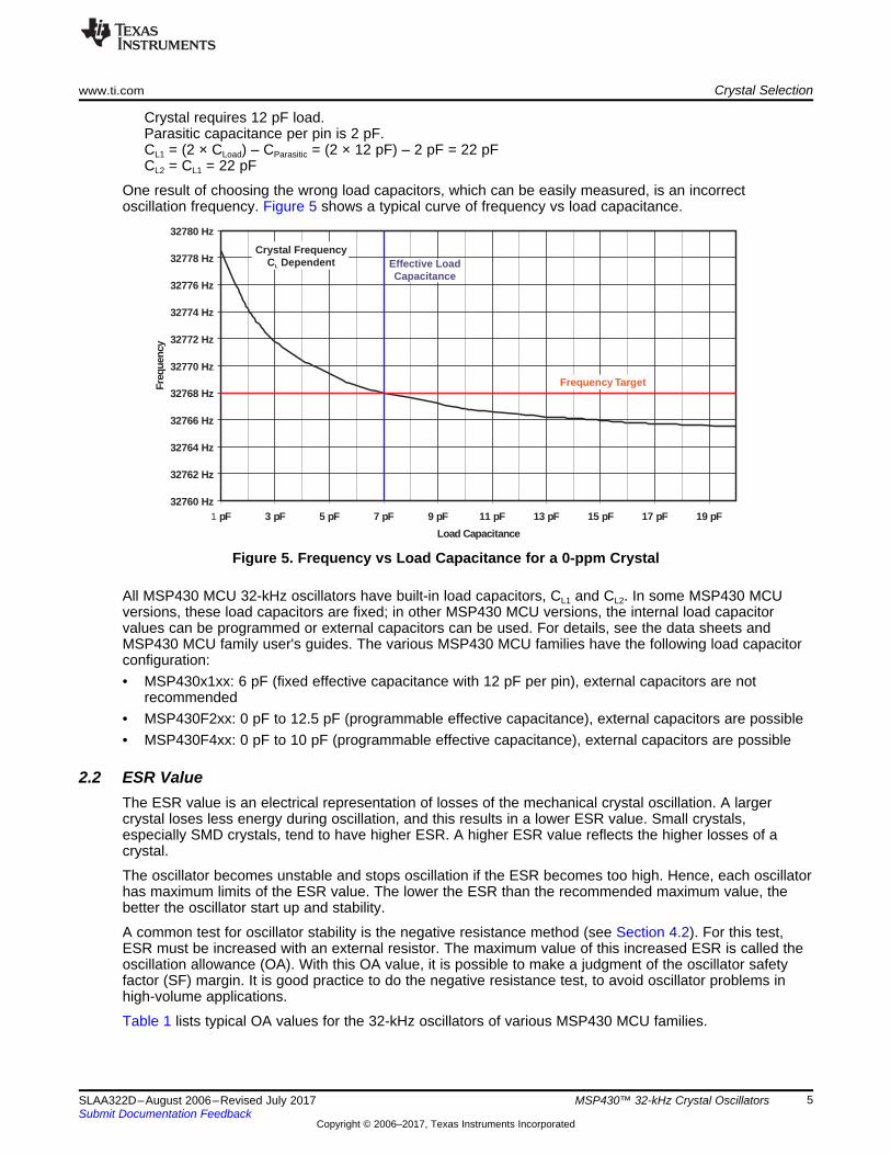
Crystal requires 12 pF load.Parasitic capacitance per pin is 2 pF.CL1 = (2 × CLoad) – CParasitic = (2 × 12 pF) – 2 pF = 22 pFCL2 = CL1 = 22 pF
One result of choosing the wrong load capacitors, which can be easily measured, is an incorrectoscillation frequency. Figure 5 shows a typical curve of frequency vs load capacitance.
Figure 5. Frequency vs Load Capacitance for a 0-ppm Crystal
All MSP430 MCU 32-kHz oscillators have built-in load capacitors, CL1 and CL2. In some MSP430 MCUversions, these load capacitors are fixed; in other MSP430 MCU versions, the internal load capacitorvalues can be programmed or external capacitors can be used. For details, see the data sheets andMSP430 MCU family user's guides. The various MSP430 MCU families have the following load capacitorconfiguration:• MSP430x1xx: 6 pF (fixed effective capacitance with 12 pF per pin), external capacitors are not
recommended• MSP430F2xx: 0 pF to 12.5 pF (programmable effective capacitance), external capacitors are possible• MSP430F4xx: 0 pF to 10 pF (programmable effective capacitance), external capacitors are possible
2.2 ESR ValueThe ESR value is an electrical representation of losses of the mechanical crystal oscillation. A largercrystal loses less energy during oscillation, and this results in a lower ESR value. Small crystals,especially SMD crystals, tend to have higher ESR. A higher ESR value reflects the higher losses of acrystal.
The oscillator becomes unstable and stops oscillation if the ESR becomes too high. Hence, each oscillatorhas maximum limits of the ESR value. The lower the ESR than the recommended maximum value, thebetter the oscillator start up and stability.
A common test for oscillator stability is the negative resistance method (see Section 4.2). For this test,ESR must be increased with an external resistor. The maximum value of this increased ESR is called theoscillation allowance (OA). With this OA value, it is possible to make a judgment of the oscillator safetyfactor (SF) margin. It is good practice to do the negative resistance test, to avoid oscillator problems inhigh-volume applications.
Table 1 lists typical OA values for the 32-kHz oscillators of various MSP430 MCU families.
-160.0 PPM
-140.0 PPM
-120.0 PPM
-100.0 PPM
-80.0 PPM
-60.0 PPM
-40.0 PPM
-20.0 PPM
0.0 PPM
-40°C -20 C° 0 C° 20°C 40 C° 60 C° 80°C
Temperature
DF
/F
T0 = 25°C ±5°C
–0.035 ppm/°C × (T – T0) ±10%2 2
Crystal Selection www.ti.com
6 SLAA322D–August 2006–Revised July 2017Submit Documentation Feedback
Copyright © 2006–2017, Texas Instruments Incorporated
MSP430™ 32-kHz Crystal Oscillators
NOTE: If oscillation allowance for LF crystals (OALF) values are specified in an MSP430 MCU datasheet, this table does not apply, and only the data sheet values are valid.
Table 1. Typical Oscillation Allowance Values for the 32-kHz Oscillator
MSP430x1xx MSP430x2xx MSP430x4xxCL = 6 pF CL = 6 pF CL = 12.5 pF CL = 6 pF CL = 12.5 pF
VCC = 3 V 185 kΩ 500 kΩ 200 kΩ 460 kΩ 180 kΩVCC = 2.2 V 88 kΩ 500 kΩ 200 kΩ 440 kΩ 170 kΩ
Refer to crystal manufacturer recommendation for 32-kHz crystals operating with MSP430 MCUoscillators.
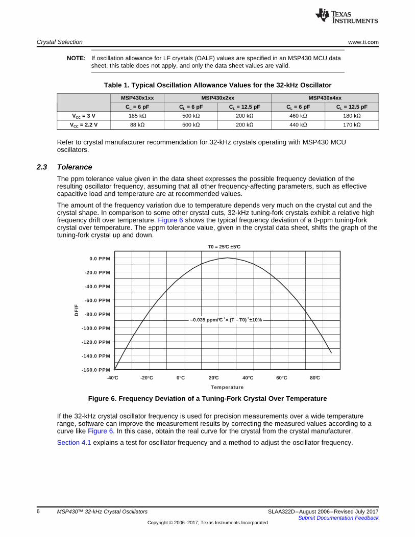
2.3 ToleranceThe ppm tolerance value given in the data sheet expresses the possible frequency deviation of theresulting oscillator frequency, assuming that all other frequency-affecting parameters, such as effectivecapacitive load and temperature are at recommended values.
The amount of the frequency variation due to temperature depends very much on the crystal cut and thecrystal shape. In comparison to some other crystal cuts, 32-kHz tuning-fork crystals exhibit a relative highfrequency drift over temperature. Figure 6 shows the typical frequency deviation of a 0-ppm tuning-forkcrystal over temperature. The ±ppm tolerance value, given in the crystal data sheet, shifts the graph of thetuning-fork crystal up and down.
Figure 6. Frequency Deviation of a Tuning-Fork Crystal Over Temperature
If the 32-kHz crystal oscillator frequency is used for precision measurements over a wide temperaturerange, software can improve the measurement results by correcting the measured values according to acurve like Figure 6. In this case, obtain the real curve for the crystal from the crystal manufacturer.
Section 4.1 explains a test for oscillator frequency and a method to adjust the oscillator frequency.
www.ti.com Crystal Selection
7SLAA322D–August 2006–Revised July 2017Submit Documentation Feedback
Copyright © 2006–2017, Texas Instruments Incorporated
MSP430™ 32-kHz Crystal Oscillators
2.4 Start-up TimeWhen initially energized, the only signal in the circuit is noise. That component of noise whose frequencysatisfies the phase condition for oscillation is propagated around the loop with increasing amplitude. Theamplitude continues to increase until the amplifier gain is reduced either by nonlinearities of the activeelements ("self-limiting Pierce", MSP430x1xx) or by some automatic level control ("controlled Pierce" withAGC circuitry, MSP430x2xx and MSP430x4xx).
Start-up times between several hundred milliseconds and a few seconds are normal values for low-frequency tuning-fork crystals, like 32768-Hz crystals. The start-up time of a crystal oscillator depends onvarious factors:• The oscillator frequency influences the start-up time. A 32-kHz crystal oscillator starts relatively slowly,
compared to a crystal oscillator with a high frequency, e.g., above 1 MHz.• High Q-factor crystal oscillators typically start slower than crystal oscillators with higher frequency
tolerance.• Crystal with low load capacitance typically start faster than crystals requiring high load capacitance.• Crystals with low ESR start more quickly than high ESR crystals.• Oscillators with high OA (Oscillation Allowance) start faster than low OA crystal oscillators.

PCB Design Considerations www.ti.com
8 SLAA322D–August 2006–Revised July 2017Submit Documentation Feedback
Copyright © 2006–2017, Texas Instruments Incorporated
MSP430™ 32-kHz Crystal Oscillators
3 PCB Design ConsiderationsThe MSP430 MCU LFXT1 32-kHz crystal oscillator is designed for ultra-low-power consumption.According to the data sheets, most MSP430 MCU derivatives consume less than 1 µA when the 32-kHzoscillator, the clock signal (ACLK), and a timer are running. Hence, the current flowing between theMSP430 MCU pins, the crystal and, if used, the external capacitors is extremely low. Long signal linesmake the oscillator very sensitive to EMC, ESD, and crosstalk. Even the best components cannot solveproblems caused by a poor layout.
The crystal oscillator is an analog circuit and must be designed according to analog-board layout rules:• Signal traces between the MSP430 MCU pins, the crystal and, if used, the external capacitors must be
as short as possible. This minimizes parasitic capacitance and sensitivity to crosstalk and EMI. Thecapacitance of the signal traces must be considered when dimensioning the load capacitors.
• Keep other digital signal lines, especially clock lines and frequently switching signal lines, as far awayfrom the crystal connections as possible. Crosstalk from digital signals may disturb the small-amplitudesine-shaped oscillator signal.
• Reduce the parasitic capacitance between XIN and XOUT signals by routing them as far apart aspossible.
• The main oscillation loop current is flowing between the crystal and the load capacitors. Keep thissignal path (crystal to CL1 to CL2 to crystal) as short as possible and use a symmetric layout. Hence,both capacitors' ground connections should always be as close together as possible. Never route theground connection between the capacitors or all around the crystal, because this long ground trace issensitive to crosstalk and EMI.
• Guard the crystal traces with ground traces (guard ring). This ground guard ring must be clean ground.This means that no current from and to other devices should be flowing through the guard ring.Connect this guard ring to AVSS of the MSP430 MCU with a short trace. Never connect the groundguard ring to any other ground signal on the board. Also avoid implementing ground loops.
• With 2-layer boards, do not route any digital-signal lines on the opposite side of the PCB under thecrystal area. In any case, it is good design practice to fill the opposite side of the PCB with cleanground and also connect this ground to AVSS of the MSP430 MCU.
• Connect the crystal housing to ground.Before soldering the crystal housing, contact the crystal manufacturer to make sure not to damage thecrystal. Overheating the crystal housing could lead to destruction of the crystal.
• In LF mode, the LFXT1 oscillator of MSP430x1xx requires a ≥5.1-MΩ resistor from XOUT to VSS whenVCC < 2.5 V. This is used to increase the drive level of the MSP430 MCU amplifier at low VCC. Refer tothe data sheet for details.
Making use of the MSP430 MCU built-in capacitors gives a simple layout, with only the crystal connectedto the XIN and XOUT pins of the MSP430 MCU. The traces between the MSP430 MCU and the crystalshould be as short as possible, and a ground area should be placed under the crystal oscillator area.When using external capacitors instead of the internal capacitors, the traces between the crystal and thecapacitors and the trace between the two capacitors should be as short as possible. Examples forrecommended layouts are shown in Figure 7. An additional ground guard ring could improve theperformance.

GND Island
isolated by a gap from
the rest of the GND
GND Island
isolated by a gap from
the rest of the GND
www.ti.com PCB Design Considerations
9SLAA322D–August 2006–Revised July 2017Submit Documentation Feedback
Copyright © 2006–2017, Texas Instruments Incorporated
MSP430™ 32-kHz Crystal Oscillators
Figure 7. Layout Without and With External Load Capacitors(XIN and XOUT Neighboring Pins Are Standard Function Pins)
Some of the MSP430 MCU have NC (not connected) pins neighboring the XIN and XOUT crystalconnection pins. In that case, it is recommended to make use of the situation and add a ground guard ringaround the crystal signals. This ground guard ring should have a short connection to the MSP430 MCUVSS pin. Layout examples for this scenario are shown in Figure 8. In all these examples, the sectionbetween crystal and the load capacitors is laid out symmetrically.
NOTE: The layout on the right side includes a resistor between XOUT and VSS. The LFXT1 oscillator ofMSP430x1xx (see data sheet) in LF-mode requires a resistor of ≥5.1 MΩ from XOUT to VSS whenVCC < 2.5 V, to compensate for decreasing drive level with lower supply voltages.
Figure 8. Layout With External Capacitors and Ground Guard Ring(XIN and XOUT Neighboring Pins Are NC Pins)
Examples for MSP430F41x and MSP430F1232IRHB

Testing the Crystal Oscillator www.ti.com
10 SLAA322D–August 2006–Revised July 2017Submit Documentation Feedback
Copyright © 2006–2017, Texas Instruments Incorporated
MSP430™ 32-kHz Crystal Oscillators
4 Testing the Crystal OscillatorThe following measurements help to verify the crystal oscillator stability:• Oscillator frequency vs load capacitance• Negative resistance method (Oscillation Allowance test)
– Start allowance– Stop allowance
4.1 Oscillator Frequency vs Load CapacitanceAs shown in Figure 5, the crystal oscillator frequency is very much dependent on the load capacitance thatis connected. Hence, measuring the oscillator frequency gives a good indication if the load capacitors thatare used match the crystal requirements. This measurement also automatically includes the parasitic PCBand pin capacitances of the application. The graph in Figure 5 shows typical 32-kHz crystalcharacteristics. The characteristics (pullability curve) of the crystal should be provided by the crystalmanufacturer.
It is strongly recommended not to measure the oscillator frequency directly at the crystal pins. Thecapacitance at the crystal pins is in the range of 10 pF, and the impedance on this signal line is severalmegaohms. A typical passive probe has a capacitance in the range of 10 pF and an input impedance ofapproximately 10 MΩ. Both values are in the range of the oscillator characteristics and heavily influencethe behavior of the crystal oscillators. The MSP430 MCU internal digital ACLK clock signal always carriesthe clock signal of the 32-kHz crystal oscillator. All MSP430 MCU have the capability to output ACLK atone of the I/O pins. Measuring at this digital ACLK output does not influence the crystal oscillator in anyway. ACLK still gives all necessary information to determine the stability and performance of the setup.
A frequency counter with a resolution and accuracy of at least 0.1 ppm in the targeted frequency rangeshould be used to measure the 32768-Hz clock signal. If, for example, the tolerance of the crystal is givenwith ±30 ppm, the 32768-Hz clock frequency should be ±0.9 Hz accurate at room temperature. For a ±5-ppm crystal, the frequency should be within ±0.16 Hz when the correct capacitive load is connected.
Assuming the crystal itself has no tolerance, too low a capacitive load results in a higher oscillatorfrequency than expected and, vice versa, the frequency is lower than the nominal value, if the load is toohigh. Hence, if the oscillation frequency is too high, the value of load capacitors must be increased. Whena too low frequency is measured, it is necessary to decrease the value of the load capacitors. Comparingthe finally optimized capacitors with the crystal data sheet value for load capacitance gives the parasiticcapacitance added by the PCB layout and pins.
4.2 Negative Resistance MethodThe negative resistance method is also called the Oscillation Allowance test or safety margin test. Withthis test, the ESR safety factor is measured. As already stated in previous sections, the ESR value in theequivalent circuit of a crystal (see Figure 2) represents the losses. These losses must be compensated bythe amplifier in the MSP430 MCU. If the losses exceed the drive capabilities of the amplifier, the oscillationamplitude starts decreasing until it finally dies away, or the oscillator does not even start up. The ESRvalue of a crystal increases with temperature. Thus, the oscillator may be working fine at roomtemperature but may fail at higher temperatures. Also, higher humidity can increase the losses in theoscillator, due to lower parasitic resistive values. To avoid time-consuming oscillator tests over all possibleenvironmental situations, the negative resistance test has been established. It gives a SF (Safety Factor)value that allows the designer to assess, relatively easily, the safety margin of a particular oscillator setup.
For the negative resistance test, an additional resistor is added in series with the crystal, as shown inFigure 9. The additional serial test resistance, RQ, is increased until the oscillator does not start up or arunning oscillation stops. It is good practice to lower the resistance until the oscillator works again, todetermine the critical value. This can be done using an SMD potentiometer that is suitable for RF, to addas few parasitic values as possible. Because all parameters and the parasitic values of this potentiometercontribute to the resulting parameters of the oscillator circuit, the final value of RQmax should be verifiedwith an SMD resistor.

SF = =R + ESRQmax
ESROA
ESR
OA = R + ESRQmax
CL1 CL2
RQ
www.ti.com Testing the Crystal Oscillator
11SLAA322D–August 2006–Revised July 2017Submit Documentation Feedback
Copyright © 2006–2017, Texas Instruments Incorporated
MSP430™ 32-kHz Crystal Oscillators
Figure 9. Negative Resistance Method With Added Resistor RQ
The test can be done during the oscillator start (Start Allowance) and it can be repeated for a runningoscillator to determine when oscillation dies away (Stop Allowance).• Start Allowance: Resistor RQ is placed in series to the crystal. The power is then turned on, and it is
checked if the oscillator starts. For each new resistor value, the MSP430 MCU must be powered downand powered up again. The highest resistor value with which the oscillator still starts is the StartAllowance.
• Stop Allowance: When the oscillator is running, the RQ potentiometer is increased until the oscillatorstops. The potentiometer can then be reduced again until the oscillation starts again. The highestresistor value with which the oscillator still runs and does not stop is the Stop Allowance.
After the critical values of RQ are measured, the OA and the SF should be calculated to allow a judgmentof the oscillator stability, as shown in Equation 4 and Equation 5.
Oscillation Allowance (OA)(4)
Safety Factor (SF)
(5)
Table 2 gives a qualification of the SF and is based on the experience of major crystal manufacturers. Ifthe outcome of the investigations is a sufficient SF, then the assumption can be made that all reasonabletolerances and variations of the parameters of the oscillator externals should be covered.
Table 2. Safety Factor
QUALIFICATION OF THESAFETY FACTOR (SF) QUALIFICATION
SF < 2 Unsafe2 ≤ SF < 3 Suitable3 ≤ SF < 5 Safe
SF ≥ 5 Very safe
4.3 Relationship Between Crystal ESR and Safety FactorTo further show the importance of ESR on a crystal's ability to oscillate properly, the negative resistancemethod detailed in Section 4.2 was used on a selection of crystal oscillators with varying packages, ESRvalues, and tolerances. The test was performed using a MSP430FE427A device populated on a MSP-TS430PM64 target board, a platform whose design does not follow the recommendations detailed by thisapplication report. The RQmax value of each crystal was determined by placing a potentiometer in seriesfollowed by testing for the crystal's start and stop allowances. The nearest standard resistor value (±5%)was recorded as general reference. The exact oscillation allowances and safety factors were also
Crystal Oscillator in Production www.ti.com
12 SLAA322D–August 2006–Revised July 2017Submit Documentation Feedback
Copyright © 2006–2017, Texas Instruments Incorporated
MSP430™ 32-kHz Crystal Oscillators
calculated using Equation 4 and Equation 5. Table 3 outlines the outcome of these tests. Note that resultswill differ based on variables such as PCB design, board cleanliness or amount of flux present, andquantity of solder used, all of which affect the system's parasitic capacitance. The size and dimensions ofall crystals used in this example are similar, but accommodations were made to establish connections tothe target board and the various package types.
(1) While some tests resulted in safety factors in the suitable and safe categories, the target boards are not ideal test fixtures due tothe socket.
Table 3. Safety Factor Test Results
Mouser Crystal PartNumber Package ESR
(kΩ)Tolerance
(±ppm)RQmax(kΩ)
StandardValue(kΩ)
OA(kΩ) SF (1)
AB26T-32.768KHZ Radial 35 20 257 240 292 8.34CFS206-32.768KEZB-U Radial 35 10 254 240 289 8.26AB26TRQ-32.768kHz-T Radial 50 20 195 180 245 4.90MC-306 32.7680K-A0 4-SOJ 35 20 233 220 268 7.66ABS25-32.768KHZ-T 4-SOJ 50 20 250 240 300 6.00CM200C-32.768KDZB-UT 4-SOJ 50 20 242 240 292 5.84ABS25-32.768KHz-6-1-T 4-SOJ 50 10 238 220 288 5.76FC-12M 32.7680KA-A3 2-SMD 90 20 178 160 268 2.98ABS10-32.768KHZ-T 2-SMD 70 20 213 200 283 4.04ABS07-32.768KHZ-1-T 2-SMD 70 10 197 180 267 3.81FC-135R 32.7680KA 2-SMD 50 20 246 240 296 5.92
As Table 3 shows, crystals with a lower ESR produce a higher RQmax, which proportionately results inhigher oscillation allowances and safety factors.
5 Crystal Oscillator in ProductionIn general, it needs to be considered that the 32-kHz crystal oscillator is an ultra-low-power oscillator withvery low current, in a range significantly below 1 µA. Thus it is critical, for the performance of the oscillator,that the PCB assembly process not introduce any materials or residue that would compromise the surfaceinsulation resistance and lead to current leakage paths. One common source of residues and unwantedmaterials is the use of "no-clean" flux and the consequent lack of cleaning in the manufacturing process.
5.1 PCB Material, Quality, and CleaningIn addition to other factors, which have been described in the previous sections and which are covered bycircuit theory, optimization of the components, and layout, there is another group of factors significantlyaffecting the performance of the oscillator setup. These factors are the board-assembly productionprocess and assembly quality. In the previous sections, the ultra-low-power character of the MSP430MCU oscillators has been mentioned. Due to the optimization for the lowest possible current, the lossescaused by parasitic currents can have a significant impact on the overall oscillator performance.
PCB quality and cleanliness are especially critical in applications with a long lifetime and underunfavorable conditions, like high humidity and fast temperature cycles that possibly cause humiditycondensation on the printed circuit board. Requiring a high level of quality and cleanliness reducesprocess residuals, which can lead to a decrease of the insulation of the sensitive oscillator signal linestowards each other and neighboring signals on the PCB. High humidity can lead to moisture condensationon the surface of the PCB and, together with process residuals, reduce the surface resistivity of the board.Thus, TI strongly recommends to carefully select the materials for the soldering process and use cleanPCB material for the assembly process and cleaning afterwards, if needed, especially when the previouslydescribed factors apply.
One specific target of cleaning is the removal of residuals associated with the flux used in soldering, whichis discussed in Section 5.2.

www.ti.com Crystal Oscillator in Production
13SLAA322D–August 2006–Revised July 2017Submit Documentation Feedback
Copyright © 2006–2017, Texas Instruments Incorporated
MSP430™ 32-kHz Crystal Oscillators
5.2 Soldering and Contact ImpedanceSoldering introduces flux materials that have the primary purpose of chemically removing oxides to ensuremetallic surfaces are joined properly with minimal contact impedance. When soldering, there are basicallytwo different types of flux material. There are water-soluble flux materials, which must be cleaned off afterthe soldering process by appropriate cleaning processes, and there are low-solid fluxes (LSF) or "noclean" flux materials on the market. For specific cleaning procedures, refer to the solder-pastemanufacturer's recommendation for the specific soldering paste and flux. The main advantages of water-soluble fluxes are that they are typically the most highly active and more effective than "no-clean"products. Being more highly active, the water-soluble fluxes support a much better wetting process whichleads to less soldering dwell time and consequently less thermal shock. The main disadvantage is the costassociated with the cleaning in the assembly process. The principle advantage of a "no-clean" product islower cost, while the disadvantage revolves around post-soldering reliability.
Even when using the "no clean" products in ultra-low-power applications, PCB cleaning is recommendedto achieve maximum performance by removing flux residuals from the board after assembly. The residualsleft behind are typically weak organic acids and oils. The weak organic acids dissolve in water makingthem sources of leakage currents and failures in humid environments. Additionally the ester oil can act asan entrapment for dust which can also act as a humidity absorber. It is important to work with yourmanufacturer to identify sensitive or precision circuits that can be impacted by flux residuals and select acleaning process to remove them. The flux residuals on the board can cause leakage current paths,especially in humid environments. In general, reduction of losses in the oscillator circuit leads to a bettersafety margin and, thus, also increases performance and reliability.
The MSP430 MCU package is qualified against JEDEC Std 020 to withstand the specified maximum peakreflow temperature allowed at certain moisture sensitivity level (MSL). This is the maximum allowed reflowprofile. The solder-paste supplier usually supplies a suggested reflow profile that is within the JEDEC Std020 maximum range. Thus, the JEDEC recommendations for the soldering profile for devices and therecommendations of the soldering materials supplier should be carefully followed, to achieve highreliability and quality solder joints.
If the MSP430 MCU package is to be exposed to any reflow temperatures after the liquid cleaningprocess, the board with the mounted MSP430 MCU package should be baked, to dry out the part beforethe following reflow process. In this case, the devices must be baked according to the JEDEC Std 020 (24hours at 125°C) before processing through an additional solder-reflow step or performing a reworksoldering.
Another important topic in the category of soldering is how to properly solder the metal housing or 'can' tothe PCB. Without proper consideration of the manufacturer's guidelines, it is possible to damage thecrystal from thermal stress. Adhering to specific guidelines can be hindered because of the large footprintthat can remove heat from the area requiring higher temperatures or longer dwell times. Again, it is criticalto adhere to the manufacturer's specification for soldering the crystal to prevent overheating anddamaging the part.
5.3 Environmental Influences, Temperature, and HumidityThe most relevant environmental influences are temperature, humidity, and airborne contaminants. Theseenvironmental influences contribute to the general breakdown and introduction of electrochemicalmigration (ECM) on the PCB. These influences can also introduce leakage paths in the crystal oscillatorcircuit. And while the impact associated with ECM are generally seen after years of operation, the impacton the low power crystal-oscillator circuit can be immediately seen with the introduction of leakage paths.This impact may range from slow start up times to a complete inability to oscillate.
Temperature, specifically higher temperatures can have both positive effects and negative effects. Apositive effect is that higher temperatures promote evaporation of weak organic acids found in fluxresidues and thus reduce leakage associated with the residue. A negative effect is that the highertemperature can reduce the drive strength of the output stage transistors thus, the safety margin of anoscillator setup decreases. As long as the safety factor test has shown good results, as classified inTable 2, and the crystal is being used in the standard industrial temperature range, the application shouldwork safely.

Crystal Oscillator in Production www.ti.com
14 SLAA322D–August 2006–Revised July 2017Submit Documentation Feedback
Copyright © 2006–2017, Texas Instruments Incorporated
MSP430™ 32-kHz Crystal Oscillators
In addition to high temperature, temperature cycles, especially fast temperature cycles combined with highambient humidity, can result in condensed water on the PCB. Condensation and humidity in generalcontribute to the degradation of the PCB. And as already discussed, the humidity is drawn to thehygroscopic residue associated with no-clean flux, resulting in leakage paths and a higher ESR for thecrystal.
Together with soldering residues and other board contaminations, dust (air-borne contaminants) can easilyaccumulate in applications with a lifetime of several years and non-air-proof housings. This debris candecrease the insulation of the oscillator signals towards each other and towards neighboring signals onthe PCB. Thus, it is a good practice to introduce a protective coating of the crystal, the attached externals,and the MSP430 MCU oscillator pins. Examples of protective coatings are conformal coating,encapsulation, and potting.
Conformal coating is more popular, providing a transparent protective layer that allows visible inspection.Silicon coatings are typically superior to urethane and acrylic, but all three types can be used to preservethe parameters and performance of the oscillator over many years of operation in the field.
Potting and encapsulation materials offer similar benefits. Typically made of silicon or polyurethane,potting provides vibration dampening, heat dissipation, security (non-transparent), and mechanicalprotection. Working with the contract manufacturer will help avoid possible issues associated with pottingmaterials coefficient of thermal expansion and the associated stress placed upon a surface mount crystal.High (>450V/mil) dielectric strength materials are recommended for coatings to ensure little or noperformance difference is seen in the crystal-oscillator circuit. Table 4 lists examples of high-dielectricmaterials.
Table 4. Example Coating Materials
Manufacturer Product Dielectric StrengthCramolin Plastik 21 kV/mm (533 V/mil)
3M™ Novec™ 1901 3700 V/milMG Chemicals 419C >1500 V for 1-mil coating per IPM-TM-650
If no coating is provided, then a continuous degradation of the oscillator performance can occur andshould be taken into account. While a very effective defense against environmental influences, the use ofprotective coatings brings back into focus the importance of board cleanliness. Protective coatingsintroduce reliability risks which are associated with the contamination trapped under the coating into whichmoisture can diffuse.
5.4 Device-Specific Features to Support Better Start-up BehaviorDue to the influences to the start-up behavior of the MSP430 MCU ULP oscillator, described in theprevious chapters, this section provides guidance to improve the overall start-up time of the low-frequencyoscillator (LFO) by adding a simple piece of code.
The background for this kickstart feature lies in the architecture of the Pierce oscillator (see Figure 4).Normally the amplifier inverts the input signal coming from the crystal and amplifies the signal to furtherexcite the tuning fork crystal to oscillate to its target frequency. Due to the ULP design and externalenvironmental conditions like crystal ESR, load capacitance, shunt capacitance, humidity, PCBcontamination, and temperature, the start-up behavior of the whole circuit might be different. This can leadto longer start-up times, which can conflict with the application requirements.
To work around this behavior, it is possible to create some kick-start noise on the amplifier output to helpthe crystal start oscillating more quickly. This is possible by simply changing the supply source of theamplifier by switching it between high-frequency mode and low-frequency mode multiple times. Thecreated output noise significantly reduces the start-up time and does not require additional effort on PCBdesign or external components. However, the general requirements for LFO design described inSection 2.1, Section 2.2, Section 3, Section 5.1, Section 5.2, and Section 5.3, need to be considered andfollowed. The described methodology is not intended to revive a crystal that is failing to start at all.

www.ti.com Crystal Oscillator in Production
15SLAA322D–August 2006–Revised July 2017Submit Documentation Feedback
Copyright © 2006–2017, Texas Instruments Incorporated
MSP430™ 32-kHz Crystal Oscillators
The method that is introduced here is also called "XTS toggling", and it simply inverts the XTS bit inside aspecific register of the clock module multiple times. Table 5 is an overview of the bit naming and thecorresponding register for applicable MSP430 MCU families. In addition to using XTS toggling, TIrecommends using the highest possible drive strength to further support a fast start-up of the crystal.
(1) This does not include the MSP430x20xx and MSP430G2xx devices, which have no shared LF/HF oscillator.
Table 5. MSP430 MCU Family Overview With Respect to XTS and Corresponding Registers
MSP430 MCU Family Bit Name Corresponding RegisterF1xx family XTS BCSCTL1
F2xx and G2xx family (1) XTS BCSCTL1F4xx family XTS_FLL FLL_CTL0
F5xx and F6xx family XTS UCSCTL6FR5xx and FR6xx No shared LF or HF oscillator availableFR2xx and FR4xx XTS CSCTL6
The code snippet written in assembler shows the implementation in software (see Figure 10). This codetoggles the XTS bit 400 times to create the described noise in the oscillator circuit to improve the start-upbehavior. The number of toggles can be varied depending on the frequency, but it should be large enoughto create enough noise to help the crystal to start. On the other side, this loop should not be too large thatit is longer than the typical start-up time of a crystal oscillator, which is in the range of 1 to 4 seconds. Thisstart-up help should applied to the crystal before the clock itself is used for any function; for example, asthe reference clock for the FLL.
Figure 10. XTS Toggle Assembler Code for an F4xx Device
This methodology was applied on four MSP430FE427 sample devices, which are known as critical withrespect to start-up time. Other devices falling into this category are:• MSP430F449 and corresponding spins• MSP430F437 and corresponding spins• MSP430FE4252 and corresponding spins• MSP430FE427A and corresponding spins• MSP430FG4270 and corresponding spins• MSP430FG439 and corresponding spins• MSP430FW427 and corresponding spins• MSP430FW429 and corresponding spins• MSP430C413 and corresponding spins

Crystal Oscillator in Production www.ti.com
16 SLAA322D–August 2006–Revised July 2017Submit Documentation Feedback
Copyright © 2006–2017, Texas Instruments Incorporated
MSP430™ 32-kHz Crystal Oscillators
All tests were performed using specific crystals with different ESR values to demonstrate the dependencyto ESR and the impact of XTS toggling. In addition, different types of PCB were used:1. The nonoptimized board was a lab PCB using socket and a connector to plug in the crystal (see
Figure 11). This board added a lot of parasitic capacitance and inductance to the oscillator system.
Figure 11. Nonoptimized PCB for General Test Purpose
2. The optimized board had the MSP device soldered on the PCB and the crystal placed as close aspossible to it following the layout guidelines described in this document (see Figure 12). This was doneto reduce the negative effect of PCB influence due to bad LFO layout.
Figure 12. PCB Optimized for Low-Frequency Oscillator Measurements

www.ti.com Crystal Oscillator in Production
17SLAA322D–August 2006–Revised July 2017Submit Documentation Feedback
Copyright © 2006–2017, Texas Instruments Incorporated
MSP430™ 32-kHz Crystal Oscillators
The results in Table 6 clearly show the positive impact of the XTS toggle sequence to the start-upbehavior of the LFO. While all four units had very long start-up times (above 16 s) on the nonoptimizedPCB, the start-up time was reduced to approximately 2.3 s on average on an optimized PCB. Thisexample shows that it very important to implement the oscillator fault flag loop before the crystal clock isused by the system to detect possible start-up issues on application level. In addition to the impact of XTStoggling, the results also show the significant impact of the PCB, which was designed according theguidelines in Section 3.
Table 6. Start-up Time Results Demonstrating the Effect of XTS Toggling Using 42-kΩ Crystal
Unit ID
Start-up Time With 42.4-kΩ Crystal (High ESR)
Nonoptimized PCBWithout XTS Toggling
Nonoptimized PCB WithXTS Toggling
Optimized PCB WithoutXTS Toggling
(seconds)
Optimized PCB With XTSToggling(seconds)
1 No start-up within 16 s No start-up within 16 s 3.40 0.732 No start-up within 16 s No start-up within 16 s 7.93 1.513 No start-up within 16 s No start-up within 16 s 2.62 0.784 No start-up within 16 s No start-up within 16 s 2.28 0.40
As a second experiment, the same measurements were taken using a different crystal with a much lowerESR. The results in Table 7 report the impact of XTS toggling using a low-ESR crystal to the LFO start-uptime. The values can be brought down to approximately 1.9 s on average, which is an additionalimprovement of 0.4 s compared to the results using a 40-kΩ crystal. This clearly shows that the PCB,crystal, and XTS all contribute to a good and acceptable start-up
Table 7. Start-up Time Results Demonstrating the Effect of XTS Toggling Using 14-kΩ Crystal
Unit ID
Start-up Time With 13.7-kΩ Crystal (Low ESR)
Nonoptimized PCBWithout XTS Toggling
Nonoptimized PCB WithXTS Toggling
Optimized PCB WithoutXTS Toggling
(seconds)
Optimized PCB With XTSToggling(seconds)
1 2.95 0.63 1.59 0.232 4.16 0.83 2.13 0.343 2.82 0.75 1.17 0.244 2.71 0.54 1.34 0.21
In conclusion, the impact of the PCB, humidity, PCB contaminations, and parameters of the used crystalneed to be considered when designing an LFO circuit with strict start-up requirements. If the start-uprequirements cannot be achieved with the traditional firmware implementation, then the use of the XTStoggling sequence might be an extra option to improve the start-up behavior.
Hardware Troubleshoot for Crystal-Oscillator Start-up in Production www.ti.com
18 SLAA322D–August 2006–Revised July 2017Submit Documentation Feedback
Copyright © 2006–2017, Texas Instruments Incorporated
MSP430™ 32-kHz Crystal Oscillators
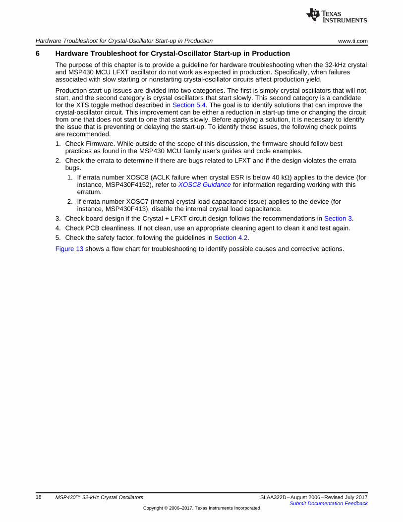
6 Hardware Troubleshoot for Crystal-Oscillator Start-up in ProductionThe purpose of this chapter is to provide a guideline for hardware troubleshooting when the 32-kHz crystaland MSP430 MCU LFXT oscillator do not work as expected in production. Specifically, when failuresassociated with slow starting or nonstarting crystal-oscillator circuits affect production yield.
Production start-up issues are divided into two categories. The first is simply crystal oscillators that will notstart, and the second category is crystal oscillators that start slowly. This second category is a candidatefor the XTS toggle method described in Section 5.4. The goal is to identify solutions that can improve thecrystal-oscillator circuit. This improvement can be either a reduction in start-up time or changing the circuitfrom one that does not start to one that starts slowly. Before applying a solution, it is necessary to identifythe issue that is preventing or delaying the start-up. To identify these issues, the following check pointsare recommended.1. Check Firmware. While outside of the scope of this discussion, the firmware should follow best
practices as found in the MSP430 MCU family user's guides and code examples.2. Check the errata to determine if there are bugs related to LFXT and if the design violates the errata
bugs.1. If errata number XOSC8 (ACLK failure when crystal ESR is below 40 kΩ) applies to the device (for
instance, MSP430F4152), refer to XOSC8 Guidance for information regarding working with thiserratum.
2. If errata number XOSC7 (internal crystal load capacitance issue) applies to the device (forinstance, MSP430F413), disable the internal crystal load capacitance.
3. Check board design if the Crystal + LFXT circuit design follows the recommendations in Section 3.4. Check PCB cleanliness. If not clean, use an appropriate cleaning agent to clean it and test again.5. Check the safety factor, following the guidelines in Section 4.2.
Figure 13 shows a flow chart for troubleshooting to identify possible causes and corrective actions.

Issues identified with PCB layout or specification review may be only part of the root cause. Therefore, it is important to also identify other potential issues and solutions before a redesign is attempted.
Slow Crystal Start-upx Candidate for firmware solution described in Section 5.4x Potential root causes
x Incompatible specificationsx PCB layoutx Material selection (applies to coatings and potting materials)x PCB cleanlinessx Damaged components: crystal or IC
No Crystal Start-upx Goal is to identify and resolve root causes to, at a minimum, move failure
to the slow crystal start-up categoryx Potential root causes
x Incompatible specificationsx PCB layoutx Material selection (applies to coatings and potting materials)x PCB cleanlinessx Damaged components: crystal or IC
Inspectionx PCB Layout
x Does layout follow guidance provided in Section 3x Are ground islands properly usedx No long runs between crystal and MSP430 MCU
x Specification Reviewx Large load capacitors can result in longer start-up timesx Large ESR crystals can result in longer start-up timesx MSP430 errata associated with family and LFXT
x PCB Cleanlinessx Removal of conformal coat or potting material and testx Clean, typically with isopropyl alcohol, and Test
PCB or Specification
x Attempt to identify the contaminantx %HRQWKHORRNRXWIRUVXEVWDQFHVDVVRFLDWHGZLWKµQR-FOHDQ¶SURGXFWVx Halides, weak organic acids, dirt, dustx Potential source in production or application
x Clean applicable areax Isopropyl alcohol or alternative cleaning agentx If a coating is present (conformal coating or potting material), then it
would be beneficial to remove the material and retest to rule out any association with the coating before cleaning. If the circuit no longer exhibits issues, then a closer investigation of the coating material is recommended but continuation along this flow is also recommended to identify other potential issues.
x Retest to identify if any improvement has been madex Pass: Acceptable start-up time or device that did not start now starts
slowlyx Fail: No change in performance
x If the PCB appears clean, then remove any conformal coating or potting material from the crystal oscillator circuit. If there is no coating material, then move to the FAIL branch below.
x Retest to identify a possible issue with the coatingx Pass: Acceptable start-up time or device that did not start now starts
slowlyx Fail: No change in performance
DIRTY CLEAN
The issue appears to be related to the cleanliness. Asses the production flow and environmental exposure to particulates (dust and dirt). As described in Section 5, parasitic leakage associated with residues and contaminates can negatively impact system performance. In systems that are contaminated by the application environment, consider using a conformal coating or potting material.
PASS FAIL
The following steps may not be feasible but are provided for completeness.x Swap test, exchange existing crystal in failing unit with
known good or previously unused crystal.x Retest to identify a possible issue with the coating
x Pass: Acceptable start-up time or device that did not start now starts slowly
x Fail: No change in performance
Investigate coating material to asses possible leakage and the source of the leakage: x Material has low breakdown voltagex Coating material is compromised or
contaminatedx Leakage material was trapped under coating
FAIL PASS
The issue appears to be associated with the crystal. Verify that the crystal has been handled properly during production, specifically with regard to the amount of heat and duration of that heat during the soldering phase. Contact your crystal manufacturer regarding thermal stress and proper manufacturing guidelines.
FAIL PASS
The issue appears to be associated with the MSP430 MCU. Up to this point the assumption has been that the issue is hardware related and not firmware. Confirm that the firmware is aligned with practices found in code examples. Additional tests should be preformed on the MSP430 MCU to ensure it was not damaged. Visit https://e2e.ti.com/support/microcontrollers/msp430/ for support.
www.ti.com Hardware Troubleshoot for Crystal-Oscillator Start-up in Production
19SLAA322D–August 2006–Revised July 2017Submit Documentation Feedback
Copyright © 2006–2017, Texas Instruments Incorporated
MSP430™ 32-kHz Crystal Oscillators
Figure 13. LFXT Troubleshooting Decision Tree

References www.ti.com
20 SLAA322D–August 2006–Revised July 2017Submit Documentation Feedback
Copyright © 2006–2017, Texas Instruments Incorporated
MSP430™ 32-kHz Crystal Oscillators
7 References1. MSP430FR4xx and MSP430FR2xx Family User's Guide2. MSP430x2xx Family User's Guide3. MSP430F2272 Device Erratasheet4. MSP430F4152 Device Erratasheet5. MSP430F413 Device Erratasheet6. XOSC8 Guidance7. IEEE Xplore, "Effect of Solder Flux Residues on Corrosion of Electronics", 20098. IEEE Xplore, "Effect of No-Clean Flux Residues on the Performance of Acrylic Conformal Coating in
Aggressive Environments", 20129. IEEE Xplore, "Surface Insulation Resistance of Conformally Coated Printed Circuit Boards Processed
with No-Clean Flux", 200610. "Selection of Wave Soldering Fluxes for Lead-Free Assembly", Shea, Arora, Brown, APEX, Los
Angeles, CA, Jan. 2007

www.ti.com Revision History
21SLAA322D–August 2006–Revised July 2017Submit Documentation Feedback
Copyright © 2006–2017, Texas Instruments Incorporated
Revision History
Revision HistoryNOTE: Page numbers for previous revisions may differ from page numbers in the current version.
Changes from June 30, 2016 to July 18, 2017 ................................................................................................................. Page
• Added the last row "FC-135R 32.7680KA" in Table 3, Safety Factor Test Results............................................. 12

IMPORTANT NOTICE FOR TI DESIGN INFORMATION AND RESOURCES
Texas Instruments Incorporated (‘TI”) technical, application or other design advice, services or information, including, but not limited to,reference designs and materials relating to evaluation modules, (collectively, “TI Resources”) are intended to assist designers who aredeveloping applications that incorporate TI products; by downloading, accessing or using any particular TI Resource in any way, you(individually or, if you are acting on behalf of a company, your company) agree to use it solely for this purpose and subject to the terms ofthis Notice.TI’s provision of TI Resources does not expand or otherwise alter TI’s applicable published warranties or warranty disclaimers for TIproducts, and no additional obligations or liabilities arise from TI providing such TI Resources. TI reserves the right to make corrections,enhancements, improvements and other changes to its TI Resources.You understand and agree that you remain responsible for using your independent analysis, evaluation and judgment in designing yourapplications and that you have full and exclusive responsibility to assure the safety of your applications and compliance of your applications(and of all TI products used in or for your applications) with all applicable regulations, laws and other applicable requirements. Yourepresent that, with respect to your applications, you have all the necessary expertise to create and implement safeguards that (1)anticipate dangerous consequences of failures, (2) monitor failures and their consequences, and (3) lessen the likelihood of failures thatmight cause harm and take appropriate actions. You agree that prior to using or distributing any applications that include TI products, youwill thoroughly test such applications and the functionality of such TI products as used in such applications. TI has not conducted anytesting other than that specifically described in the published documentation for a particular TI Resource.You are authorized to use, copy and modify any individual TI Resource only in connection with the development of applications that includethe TI product(s) identified in such TI Resource. NO OTHER LICENSE, EXPRESS OR IMPLIED, BY ESTOPPEL OR OTHERWISE TOANY OTHER TI INTELLECTUAL PROPERTY RIGHT, AND NO LICENSE TO ANY TECHNOLOGY OR INTELLECTUAL PROPERTYRIGHT OF TI OR ANY THIRD PARTY IS GRANTED HEREIN, including but not limited to any patent right, copyright, mask work right, orother intellectual property right relating to any combination, machine, or process in which TI products or services are used. Informationregarding or referencing third-party products or services does not constitute a license to use such products or services, or a warranty orendorsement thereof. Use of TI Resources may require a license from a third party under the patents or other intellectual property of thethird party, or a license from TI under the patents or other intellectual property of TI.TI RESOURCES ARE PROVIDED “AS IS” AND WITH ALL FAULTS. TI DISCLAIMS ALL OTHER WARRANTIES ORREPRESENTATIONS, EXPRESS OR IMPLIED, REGARDING TI RESOURCES OR USE THEREOF, INCLUDING BUT NOT LIMITED TOACCURACY OR COMPLETENESS, TITLE, ANY EPIDEMIC FAILURE WARRANTY AND ANY IMPLIED WARRANTIES OFMERCHANTABILITY, FITNESS FOR A PARTICULAR PURPOSE, AND NON-INFRINGEMENT OF ANY THIRD PARTY INTELLECTUALPROPERTY RIGHTS.TI SHALL NOT BE LIABLE FOR AND SHALL NOT DEFEND OR INDEMNIFY YOU AGAINST ANY CLAIM, INCLUDING BUT NOTLIMITED TO ANY INFRINGEMENT CLAIM THAT RELATES TO OR IS BASED ON ANY COMBINATION OF PRODUCTS EVEN IFDESCRIBED IN TI RESOURCES OR OTHERWISE. IN NO EVENT SHALL TI BE LIABLE FOR ANY ACTUAL, DIRECT, SPECIAL,COLLATERAL, INDIRECT, PUNITIVE, INCIDENTAL, CONSEQUENTIAL OR EXEMPLARY DAMAGES IN CONNECTION WITH ORARISING OUT OF TI RESOURCES OR USE THEREOF, AND REGARDLESS OF WHETHER TI HAS BEEN ADVISED OF THEPOSSIBILITY OF SUCH DAMAGES.You agree to fully indemnify TI and its representatives against any damages, costs, losses, and/or liabilities arising out of your non-compliance with the terms and provisions of this Notice.This Notice applies to TI Resources. Additional terms apply to the use and purchase of certain types of materials, TI products and services.These include; without limitation, TI’s standard terms for semiconductor products http://www.ti.com/sc/docs/stdterms.htm), evaluationmodules, and samples (http://www.ti.com/sc/docs/sampterms.htm).
Mailing Address: Texas Instruments, Post Office Box 655303, Dallas, Texas 75265Copyright © 2018, Texas Instruments Incorporated