multi die integration – can material suppliers meet the ... - dow.pdfmulti die integration – can...
TRANSCRIPT

Multi Die Integration – Can Material Suppliers Meet the Challenge? Nov 14, 2012 Jeff Calvert - R&D Director, Advanced Packaging Technologies Dow Electronic Materials
Passionately Innovating With Customers To Create A Connected World

Outline
Introduction
- Market Trend
- Materials Needs and Challenges
Key Materials Solutions - Examples
- Cu TSV Filling
- Temporary Wafer Bonding Adhesive
Summary
2 J. Calvert, MEPTEC Multi-Die Integration, 11/14/12
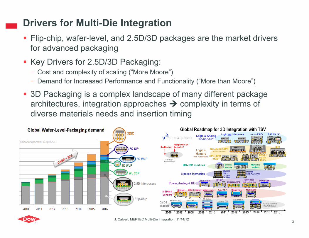
Drivers for Multi-Die Integration Flip-chip, wafer-level, and 2.5D/3D packages are the market drivers
for advanced packaging
Key Drivers for 2.5D/3D Packaging: - Cost and complexity of scaling (“More Moore”) - Demand for Increased Performance and Functionality (“More than Moore”)
3D Packaging is a complex landscape of many different package architectures, integration approaches complexity in terms of diverse materials needs and insertion timing
3 J. Calvert, MEPTEC Multi-Die Integration, 11/14/12
Global Roadmap for 3D Integration with TSV

Dow Materials for the 3DIC and WLP Market
OVERLAP between FE / BE
Supplied by Dow Semiconductor Technologies Supplied by Dow Advanced
Packaging Technologies
Supplied by Dow Metalorganic Technologies
J. Calvert, MEPTEC Multi-Die Integration, 11/14/12 4

Key Material Challenges for 3D Packaging
High AR Cu via filling, planarization Fine pitch bump metallization (solder, Cu pillar) Low stress/low cure temperature dielectrics
Improved bond/de-bond adhesives New underfill technology Thermal management
J. Calvert, MEPTEC Multi-Die Integration, 11/14/12 5

Cu TSV Development Overview
6
J. Calvert, MEPTEC Multi-Die Integration, 11/14/12
INTERLINKTM 9200 Cu TSV Plating Bath was developed to address:
1) Void-free filling of 5-20µm diameter vias, AR 5-10
2) Defect-free, low overburden deposits
Diameter, um: 21 20 19 12 11 10 8 7 6
TSV Array: 20x115µm........... .....to................6x65µm
Cu TSV Plating Bath Development
OEM POR
300mm Process Development,
Customer Demos
Chemistry Optimization: Gap filling, defects, OB,
deposit morphology
R&D Formulation Development
Fab Testing, Qualification
Customer Evaluation
Chemistry is designed for enhanced filling of TSV features, targeting a wide range of via diameters and ARs

INTERLINK™ 9200 Cu TSV Plating Bath Components
Electrolyte: Copper Sulfate/Sulfuric Acid based - IL9200 Electrolyte: 60 g/L Cu, 50 g/L Sulfuric Acid, 80 ppm Cl-
3-component Additive System - Interlink 9200 Accelerator: Electrocatalyst for bottom-up filling - Interlink 9200 Suppressor: Suppresses deposition in field, along sidewalls - Interlink Leveler: Minimizes local “mounding” over feature arrays to enhance
planarization
Interlink 9200 Pre-Wet Solution Optional vacuum/immersion process to expel air and wet seed layer If DI
wafer pre-wet is not sufficient
7 J. Calvert, MEPTEC Multi-Die Integration, 11/14/12

TSV Cu Via Filling: 5 x 50µm Features
8 J. Calvert, MEPTEC Multi-Die Integration, 11/14/12
11 .00 min 13.55 min 14.93 min
Gap Filling Speed Tests in Dow Membrane Cell
Partial Filling Sequence
Strong polarization at feature opening and sidewall suppression leads to optimum gapfilling performance
Excellent kinetics of fill at times of 15min or less
Test vehicles courtesy of Applied Materials

TSV Cu Via Filling: 10 x 100µm Features
9 J. Calvert, MEPTEC Multi-Die Integration, 11/14/12
3kÅ Fill 5kÅ Fill 7.5kÅ Fill 1.5kÅ Fill
Gap Filling Speed Test in Dow Membrane Cell
Partial Filling Sequence
Applied Materials Confidential Test vehicles courtesy of Applied Materials
Excellent gap filling kinetics for 10x100µm vias - Strong bottom-up filling - Complete filling achieved with 38 min plating cycle
1.5µm Fill (38 min)
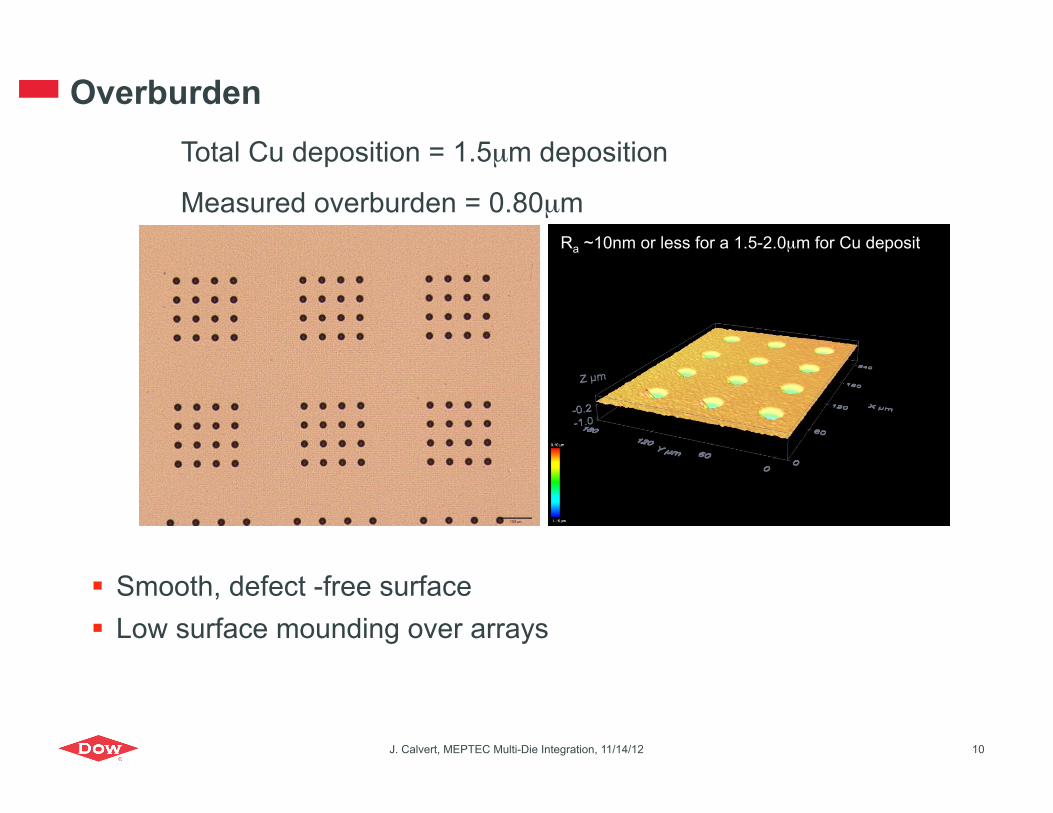
Overburden
10 J. Calvert, MEPTEC Multi-Die Integration, 11/14/12
Ra ~10nm or less for a 1.5-2.0µm for Cu deposit
Total Cu deposition = 1.5µm deposition
Measured overburden = 0.80µm
Smooth, defect -free surface Low surface mounding over arrays

Cu TSVs Annealed at 400oC for 30 min
11 J. Calvert, MEPTEC Multi-Die Integration, 11/14/12
Excellent morphology observed with large full-width Cu grains Void-free post anneal film high purity Cu deposit
Images used compliments of Applied Materials
5x50µm 10x100µm

Cu TSV Plating Bath Summary
New product developed for Cu TSV Viafilling
Excellent filling performance for interposer and via middle applications
Fast filling times and low overburden lower CoO
Void-free filling, low defects, high purity deposit high reliability/yield
300mm POR development underway at equipment vendors
J. Calvert, MEPTEC Multi-Die Integration, 11/14/12 12

Key Material Challenges for 3D Packaging
High AR Cu via filling, planarization Fine pitch bump metallization (solder, Cu pillar) Low stress/low cure temperature dielectrics
Improved bond/de-bond adhesives New underfill technology Thermal management
J. Calvert, MEPTEC Multi-Die Integration, 11/14/12 13

Key Features of XP-BCB Temporary Bonding Adhesive
Based on BCB resin technology: Well-established in manufacturing as a permanent bonding adhesive material
- High thermal stability, <1.0% wt loss/hr @ 300oC, Tg >400oC
- Resistant to most chemical etchants, solvents and strippers
- Excellent planarization over topography, low melt viscosity,
- Void-free bonding, low temperature cure (200-230oC)
- BCB platform known to be compatible with FBEOL processing, including backside grinding and plasma etching
Added features of new product for temporary bonding application:
- Single coatings 50µm, Double coating 100µm
- Differential interfacial adhesion, tunable fracture energy
- Clean, RT mechanical debonding from bumped die (Cu Pillar, C4 bump)
J. Calvert, MEPTEC Multi-Die Integration, 11/14/12 14

XP-BCB Temporary Bonding Adhesive Process Flow
Spin-on adhesive bonding layer XP-BCB Spin-on adhesion promoter
Carrier Wafer
Bond Wafers
Room temperature mechanical lift off
Thin and backside process device wafer
Device Wafer with Solder Balls 760µm thick
Thinned Device Wafer 20-100µm thick
15 J. Calvert, MEPTEC Multi-Die Integration, 11/14/12

XP-BCB Two-Layer Coating Process Example
Center Dispense
Spin-On
Soft-Bake 2 min @ 120oC
Center Dispense
Spin-On
Soft-Bake 2 min @ 120oC
1ST Coating
2nd Coating
After soft-bake
Thickness - 74.5 µm Std. Dev% - 1.03%
1.4 um
*4.5 mm scan
Target Thickness ~ 80 um
Coating Process Blank Wafer Bumped Wafer
J. Calvert, MEPTEC Multi-Die Integration, 11/14/12 16
Bake ~10 min @ 140oC Soft Cure
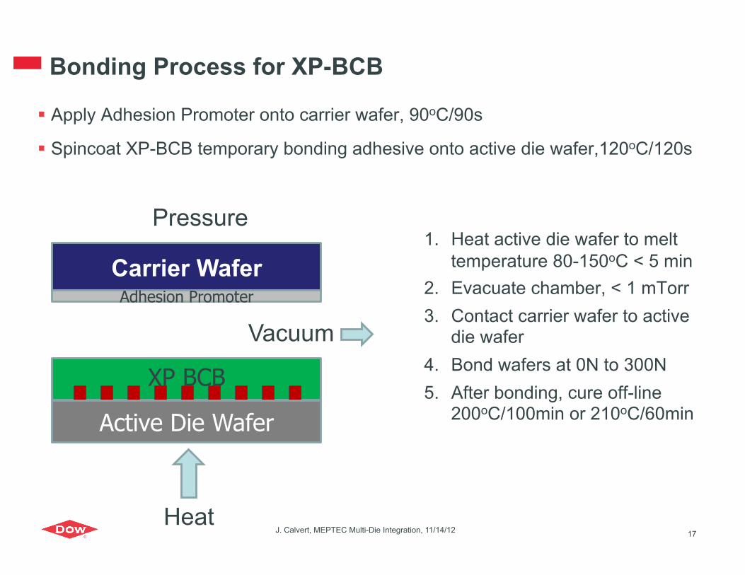
Bonding Process for XP-BCB
Apply Adhesion Promoter onto carrier wafer, 90oC/90s
Spincoat XP-BCB temporary bonding adhesive onto active die wafer,120oC/120s
XP BCB
Active Die Wafer
Vacuum
Pressure 1. Heat active die wafer to melt
temperature 80-150oC < 5 min 2. Evacuate chamber, < 1 mTorr 3. Contact carrier wafer to active
die wafer 4. Bond wafers at 0N to 300N 5. After bonding, cure off-line
200oC/100min or 210oC/60min
Heat
Carrier Wafer Adhesion Promoter
J. Calvert, MEPTEC Multi-Die Integration, 11/14/12 17
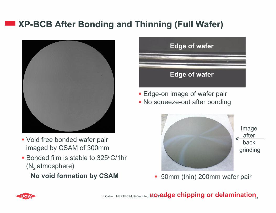
XP-BCB After Bonding and Thinning (Full Wafer)
J. Calvert, MEPTEC Multi-Die Integration, 11/14/12 18
XP-BCB After Bonding and Thinning (Full Wafer)
Void free bonded wafer pair imaged by CSAM of 300mm
Bonded film is stable to 325oC/1hr (N2 atmosphere)
No void formation by CSAM 50mm (thin) 200mm wafer pair
no edge chipping or delamination
Edge-on image of wafer pair No squeeze-out after bonding
Image after back
grinding
Edge of wafer
Edge of wafer
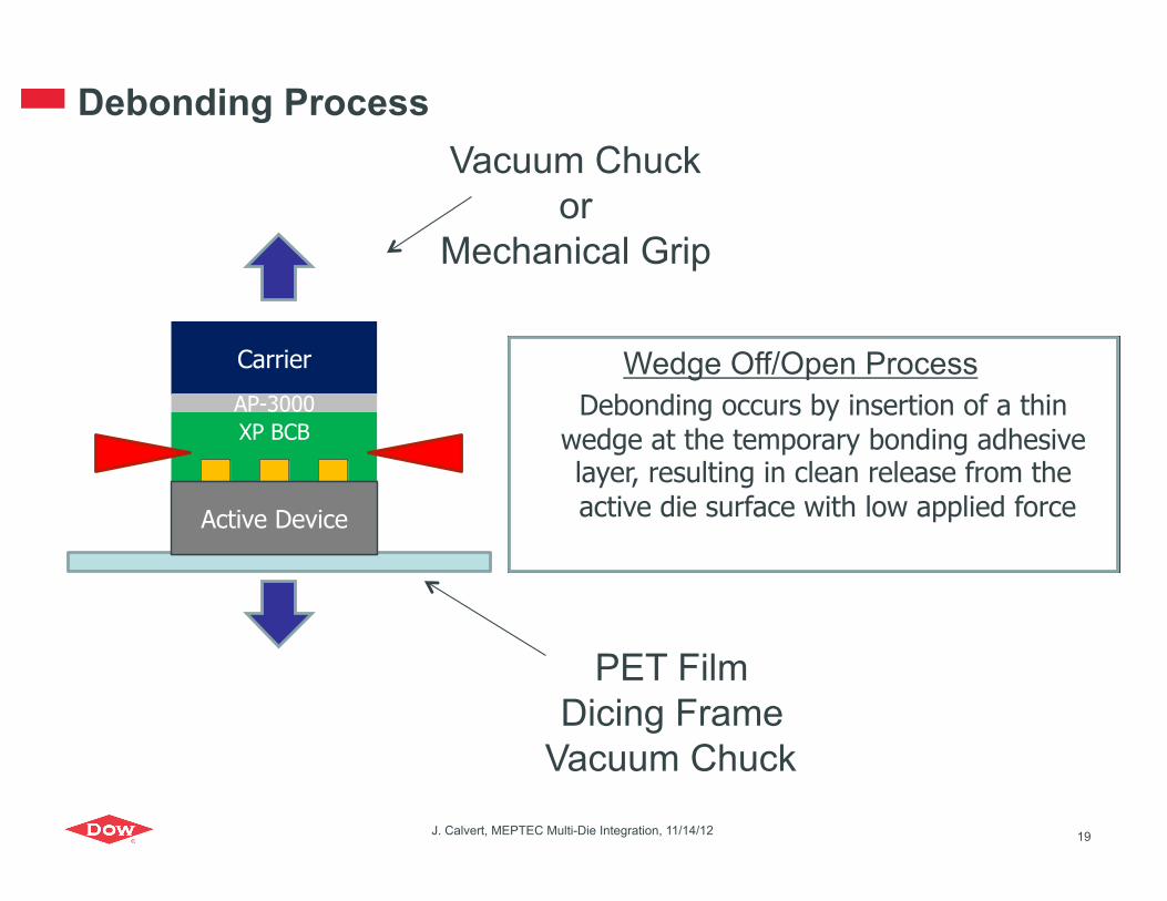
Debonding Process
J. Calvert, MEPTEC Multi-Die Integration, 11/14/12 19
Carrier
XP BCB AP-3000
PET Film Dicing Frame
Vacuum Chuck
Vacuum Chuck or
Mechanical Grip
Active Device
Debonding occurs by insertion of a thin wedge at the temporary bonding adhesive layer, resulting in clean release from the active die surface with low applied force
Wedge Off/Open Process

Blank Wafer Debonding Example
XP-BCB separated cleanly from the “active die” wafer to the carrier wafer during “wedge-off” debonding process
300mm wafers (full thickness)
Carrier Wafer “Active Die” Wafer (full thickness)
J. Calvert, MEPTEC Multi-Die Integration, 11/14/12 20
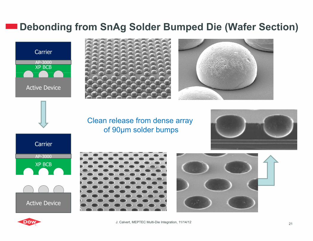
Debonding from SnAg Solder Bumped Die (Wafer Section)
J. Calvert, MEPTEC Multi-Die Integration, 11/14/12 21
Carrier
XP BCB
Active Device
AP-3000
Carrier
XP BCB
Active Device
AP-3000
Clean release from dense array of 90µm solder bumps
XP-BCB Temporary Bonding Adhesive Summary
XP-BCB is a modified formulation, based on BCB. BCB is well-known to be an effective permanent bonding adhesive
material As a temporary bonding adhesive, XP-BCB has demonstrated: - Good coating uniformity, void-free bonding, high thermal stability - High resistance to chemical and plasma processing steps - Tunable fracture energy, differential interfacial adhesion - Withstands backgrinding to 50µm - Clean debonding from bumped wafers with no apparent residue - Initial coat/bond/debond feasibility demonstrated wafers using
300mm production toolsets Work is in progress to develop a POR using 300mm bumped wafers
through backside integration
J. Calvert, MEPTEC Multi-Die Integration, 11/14/12 22

Overall Summary
2.5D/3D is a complex landscape with many different materials requirements
Key areas with emerging materials needs include: via formation/filling, wafer thinning, wafer handling (bonding/debonding), assembly, redistribution, etc.
Materials suppliers have successfully utilized existing material platforms to develop new products customized for these applications - Examples: TSV Cu filling, Temporary Bonding Adhesive
Continuous improvement needed to improve CoO - Increase yield, throughput
- Reduce process complexity
J. Calvert, MEPTEC Multi-Die Integration, 11/14/12 23

Thank You
“® ™ Registered Trademark of The Dow Chemical Company.”