multilayer pcb resin flow compensation an2011.3
TRANSCRIPT


AN2011_3 Multilayer PCB - Resin Flow Compensation
© 2011 In-Circuit Design Pty Ltd | Australia | www.icd.com.au Page 1
Multilayer PCB - Resin Flow Compensation by Barry Olney | In-Circuit Design Pty Ltd |Australia
This Application Note details techniques for accurately predicting dielectric
thickness, overall total board thickness and impedance due to resin flow
Until now, Multilayer PCB Fabrication Shops have use experience and skill to achieve specific
dielectric thickness and total board thickness, whilst maintaining impedance at an acceptable level,
from their fabrication process. To some this is a ‘black art’ better left to experienced lamination
supervisors. This approach has worked fairly well where the jobs were long running with wide
tolerances and adjustment could be made over time to improve their accuracy. However, today’s
PCB fabrication industry is quite different with high density interconnect (HDI) boards incorporating
micovias, multiple controlled impedance and differential traces, fine line technology, tighter
tolerances and short life cycles.
Acknowledging the need for more accurate methods to determine these factors, In-Circuit Design
has improved the 2011 release of the ICD Stackup Planner to incorporate compensation for prepreg
resin flow during the fabrication process.
The accuracy of impedance calculation depends on many factors. Some of these are out of the
control of Engineers or PCB Designers and are largely dependent on the fabrication processes but
fabricators now have the ability to accurately determine what to expect from any given build relative
to thickness and resin fill.
The most popular dielectric material is FR4 and may be in the form of core or prepreg (pre-
impregnated) material.
• The core material is thin dielectric (cured fibreglass epoxy resin) with copper foil bonded to
both sides. Core material may be replaced by cured prepreg in a buildup-type Microvia
stackup.
• The prepreg material is multiple thin sheets of fibreglass impregnated with uncured epoxy
resin which hardens when heated and pressed during the PCB fabrication process.
The most conventional stackup, called the ‘Foil Method’, is to have prepreg with copper foils bonded
to the outer most layers (top and bottom) then core alternating with prepreg throughout the
substrate. The result of the fabrication process is that the copper pattern is embedded into the
malleable, prepreg layer. This not only reduces the thickness of the prepreg and hence total board
thickness but also changes the impedance by a significant amount.
The factors that determine prepreg dielectric thickness are:
1. Copper Trace Density (routing density)
2. Dielectric Style
3. Resin Content
4. Resin Flow
One of the most obvious, but often forgotten, considerations in determining the prepreg thickness
yield is copper trace density. Copper weight (or thickness) is only part of the equation.

AN2011_3 Multilayer PCB - Resin Flow Compensation
© 2011 In-Circuit Design Pty Ltd | Australia | www.icd.com.au Page 2
Basically, the amount of copper on the signal layers is determined by the trace density. Signals layers
generally have ~25% coverage of copper after etching (this may be increased if copper pours or thick
power traces are used) and planes layers generally have ~80% coverage of copper with the
remainder being antipads and isolation for split planes etched from the copper.
Example: Embedded Stripline Configuration between Signal and Plane layers
Final Prepreg Thickness = H – [T1 x (100% – Trace Density %)] – [T2 x (100% - Plane Density %)]
= 5 – [1.4 x (1.0 – 0.25)] – [1.4 x (1.0 – 0.80)]
= 3.67 MIL
where
H is the dielectric thickness
T1 is the signal layer copper thickness
T2 is the plane layer copper thickness
Trace Density % is the percentage of copper on the signal layer
Plane Density % is the percentage of copper on the signal layer
In the first picture below, if we have prepreg thickness of 5 MIL then the impedance is 45.2 ohm.
If we change this 5 MIL to 3.67 MIL (from the equation above) the impedance is 41.89 ohm.
Calculating the final prepreg thickness for embedded stripline
In the second picture above, the ICD Stackup Planner calculates this automatically when
‘Compensate for Prepreg Resin Flow’ is employed. And of course, the derating gets quite
complicated depending on the slider settings, number of layers, dielectric and copper thickness,
adjacent core or prepreg materials, Foil, Capped or Built-up Technology and the stackup
configuration.
For instance using the ‘Foil Method’, prepreg with copper foil is bonded to the outside on the outer
most layers (top and bottom). This foil is etched after the substrate is cured. So therefore, there will
be no resin flow between the traces on the outer signal layers during manufacture. So, this has to be
accounted for in the calculation.
AN2011_3 Multilayer PCB - Resin Flow Compensation
© 2011 In-Circuit Design Pty Ltd | Australia | www.icd.com.au Page 3
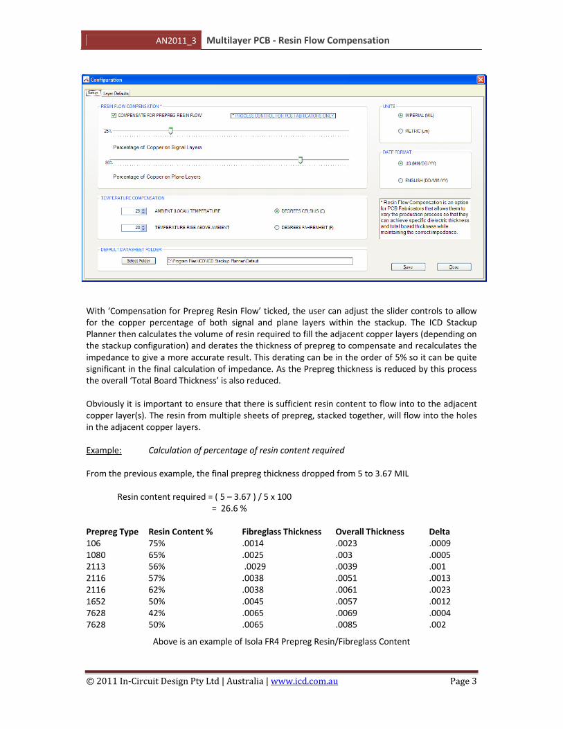
With ‘Compensation for Prepreg Resin Flow’ ticked, the user can adjust the slider controls to allow
for the copper percentage of both signal and plane layers within the stackup. The ICD Stackup
Planner then calculates the volume of resin required to fill the adjacent copper layers (depending on
the stackup configuration) and derates the thickness of prepreg to compensate and recalculates the
impedance to give a more accurate result. This derating can be in the order of 5% so it can be quite
significant in the final calculation of impedance. As the Prepreg thickness is reduced by this process
the overall ‘Total Board Thickness’ is also reduced.
Obviously it is important to ensure that there is sufficient resin content to flow into to the adjacent
copper layer(s). The resin from multiple sheets of prepreg, stacked together, will flow into the holes
in the adjacent copper layers.
Example: Calculation of percentage of resin content required
From the previous example, the final prepreg thickness dropped from 5 to 3.67 MIL
Resin content required = ( 5 – 3.67 ) / 5 x 100
= 26.6 %
Prepreg Type Resin Content % Fibreglass Thickness Overall Thickness Delta
106 75% .0014 .0023 .0009
1080 65% .0025 .003 .0005
2113 56% .0029 .0039 .001
2116 57% .0038 .0051 .0013
2116 62% .0038 .0061 .0023
1652 50% .0045 .0057 .0012
7628 42% .0065 .0069 .0004
7628 50% .0065 .0085 .002
Above is an example of Isola FR4 Prepreg Resin/Fibreglass Content

AN2011_3 Multilayer PCB - Resin Flow Compensation
© 2011 In-Circuit Design Pty Ltd | Australia | www.icd.com.au Page 4
The ICD Stackup Planner will account for a maximum of 40% unsupported resin using the default
percentages of copper on signal (25%) and plane (80%) layers so any of the above Isola prepregs or
combinations will suffice. Care should be taken when using less than 20% trace density.
Accurate prediction of dielectric thickness, overall total board thickness and impedance depend on
many critical factors. These factors can be modeled using mathematics but it is extremely time
consuming and error prone. Some of these factors are out of the control of Engineers or PCB
Designers and are largely dependent on the fabrication processes but fabricators now have the
ability to determine what to expect from any given build relative to thickness and resin fill.
The ICD Stackup Planner – Fabricator Edition allows the user to accurately determine the above
factors and does not rely on the supervisor’s experience or skill. Expensive, time consuming first
article fabrication techniques can be eliminated and stackup configurations can be designed that will
meet the customer’s requirements more accurately and consistently. Also, manufacturability and
cost can be evaluated before construction, not through a trial and error process, saving both time
and money.
For further information, please contact Barry Olney | +61 4123 14441 | [email protected]
References:
Multilayer PCB Stackup Planning – Barry Olney
Advanced Design for SMT – Barry Olney
ICD Stackup Planner – In-Circuit Design Pty Ltd (available for download @ www.icd.com.au )
Multilayer Dielectric Thickness Calculation – Tony Senese
Prepreg Resin Flow - Isola
All consideration has been taken to ensure that this Application Note is accurate, based on the information and data available. The liability
of In-Circuit Design Pty Ltd is limited to correcting any unforeseen errors and revising the Application Note to meet the specified
requirements. In no event shall In-Circuit Design Pty Ltd be liable for indirect, special, incidental, punitive or consequential damages
including but not limited to whether occasioned by the act, breach, omission, default or negligence of In-Circuit Design Pty Ltd, its
employees, contractors and subcontractors, and shall include without limitation, loss of business, revenue or profits, loss of use or data, loss
of savings or anticipated savings, loss of investments, loss of goodwill, loss of reputation or cost of capital or loss of extra administrative
cost, or economic loss, whether or not foreseeable, and arising out of or in connection with this Application Note. All trademarks are
registered trademarks of their respective owners. E&OE