namc-sdh technical reference manual - · pdf filenamc-sdh – technical reference manual...
TRANSCRIPT

NAMC-SDH – Technical Reference Manual
NAMC-SDH
Telecom AMC Module
Technical Reference Manual V1.1
HW Revision 1.x

NAMC-SDH – Technical Reference Manual
Version 1.1 © N.A.T. GmbH 2
The NAMC-SDH has been designed by:
N.A.T. GmbH
Konrad-Zuse-Platz 9
53227 Bonn
Phone: +49 / 228 / 965 864 - 0
Fax: +49 / 228 / 965 864 - 10
Internet: http://www.nateurope.com

NAMC-SDH – Technical Reference Manual
Version 1.1 © N.A.T. GmbH 3
Disclaimer
The following documentation, compiled by N.A.T. GmbH (henceforth called N.A.T.),
represents the current status of the product´s development. The documentation is
updated on a regular basis. Any changes which might ensue, including those necessitated
by updated specifications, are considered in the latest version of this documentation.
N.A.T. is under no obligation to notify any person, organization, or institution of such
changes or to make these changes public in any other way.
We must caution you, that this publication could include technical inaccuracies or
typographical errors.
N.A.T. offers no warranty, either expressed or implied, for the contents of this
documentation or for the product described therein, including but not limited to the
warranties of merchantability or the fitness of the product for any specific purpose.
In no event will N.A.T. be liable for any loss of data or for errors in data utilization or
processing resulting from the use of this product or the documentation. In particular,
N.A.T. will not be responsible for any direct or indirect damages (including lost profits,
lost savings, delays or interruptions in the flow of business activities, including but not
limited to, special, incidental, consequential, or other similar damages) arising out of the
use of or inability to use this product or the associated documentation, even if N.A.T. or
any authorized N.A.T. representative has been advised of the possibility of such
damages.
The use of registered names, trademarks, etc. in this publication does not imply, even in
the absence of a specific statement, that such names are exempt from the relevant
protective laws and regulations (patent laws, trade mark laws, etc.) and therefore free
for general use. In no case does N.A.T. guarantee that the information given in this
documentation is free of such third-party rights.
Neither this documentation nor any part thereof may be copied, translated, or reduced to
any electronic medium or machine form without the prior written consent from N.A.T.
GmbH.
This product (and the associated documentation) is governed by the N.A.T. General
Conditions and Terms of Delivery and Payment.
Note:
The release of the Hardware Manual is related to a certain HW board
revision given in the document title. For HW revisions earlier than the one
given in the document title please contact N.A.T. for the corresponding older
Hardware Manual release.
NAMC-SDH – Technical Reference Manual
Version 1.1 © N.A.T. GmbH 4
Table of Contents
TABLE OF CONTENTS .......................................................................................... 4
LIST OF TABLES .................................................................................................. 6
LIST OF FIGURES ................................................................................................ 6
CONVENTIONS .................................................................................................... 7
1 INTRODUCTION ........................................................................................... 9
2 OVERVIEW ................................................................................................. 10
2.1 MAJOR FEATURES ........................................................................................10 2.2 BLOCK DIAGRAM ........................................................................................11 2.3 LOCATION DIAGRAM ....................................................................................12
3 BOARD FEATURES ...................................................................................... 13
3.1 FPGA .....................................................................................................13 3.1.1 SDH Interface ..................................................................................13 3.1.2 Time-Slot-Interchanger (TSI) .............................................................13 3.1.3 ITDM Controller ................................................................................14 3.1.4 HDLC Controller (optional) .................................................................14 3.1.5 Control Interface ..............................................................................14 3.1.6 Ethernet Interface(s) ........................................................................15 3.1.7 Clock Connectivity ............................................................................15
3.2 SDH CHIPSET AND LINE INTERFACES ................................................................16 3.3 FPGA EXTERNAL MEMORY .............................................................................17
3.3.1 Dual External SRAM (QDR2+) ............................................................17 3.3.2 DDR3 SDRAM ...................................................................................17
3.4 AMC CLOCK INTERFACE ................................................................................17 3.5 IPMB-INTERFACE AND I2C-DEVICES .................................................................18
4 HARDWARE ................................................................................................ 19
4.1 AMC PORT DEFINITION ................................................................................19 4.2 FRONT PANEL AND LEDS ...............................................................................20 4.3 CONNECTORS AND SWITCHES .........................................................................21
4.3.1 S1: AMC Connector ...........................................................................22 4.3.2 JP1: Atmel Programming Header ........................................................24 4.3.3 J1-J4: Front Panel SFP Connectors ......................................................24 4.3.4 SW1: Hot Swap Switch ......................................................................25 4.3.5 DIP SW2: Ethernet Options Select ......................................................25
4.3.5.1 DIP SW2: Switch 1 – LIF Operation Mode Select........................................... 26 4.3.5.2 DIP SW2: Switch 2 – Backplane Ethernet Select ........................................... 26 4.3.5.3 DIP SW2: Switch 3 – Fat Pipe Select ........................................................... 27 4.3.5.4 DIP SW2: Switch 4 – MAC-Address Value Bit 0 ............................................. 27 4.3.5.5 DIP SW2: Switch 5 – MAC-Address Value Bit 1 ............................................. 28 4.3.5.6 DIP SW2: Switch 6 – External Memory Reset ............................................... 28 4.3.5.7 DIP SW2: Switch 7 – Ethernet Auto-Negotiation ........................................... 29 4.3.5.8 DIP SW2: Switch 8 – MAC-Address Configuration ......................................... 29
5 NAMC-SDH PROGRAMMING NOTES ............................................................ 30
NAMC-SDH – Technical Reference Manual
Version 1.1 © N.A.T. GmbH 5
5.1.1 0x0000000 – FUNC_TYPE/PCB_VERS ..................................................32 5.1.2 0x0000002 – FPGA_VERS ..................................................................32 5.1.3 0x0000004 – MAGIC_VAL_1 ..............................................................32 5.1.4 0x0000006 – MAGIC_VAL_2 ..............................................................32 5.1.5 0x0000008 – BOARD_ID ...................................................................33 5.1.6 0x000000A – INIT/CALIB ..................................................................33 5.1.7 0x000000C – IRQ_STAT ....................................................................34 5.1.8 0x000000E – AUTO_RD_BYTES ..........................................................34 5.1.9 0x0000010 – CARRIER_ID/GEO_ADDRESS ..........................................34 5.1.10 0x0000012 – ATMEL_EXT_INFO .........................................................35 5.1.11 0x0000014 – DIP_SW_STAT ..............................................................35 5.1.12 0x0000100 – RESET .........................................................................36 5.1.13 0x0000102 – SFP_LED_CTRL .............................................................37 5.1.14 0x0000106 – PLL_155_CLKSEL ..........................................................37 5.1.15 0x000010A – SBI_CTRL ....................................................................38 5.1.16 0x000010C – IRQ_EN .......................................................................38 5.1.17 0x000010E – TCLK_CTRL ..................................................................39 5.1.18 0x0000110 – PLL_IC2_SEL ................................................................39 5.1.19 0x000011E – BOARD_INIT_STAT .......................................................40
5.2 FPGA GBE/ITDM CONFIGURATION ..................................................................41
6 BOARD SPECIFICATION ............................................................................. 42
7 INSTALLATION .......................................................................................... 43
7.1 SAFETY NOTE ............................................................................................43 7.2 INSTALLATION PREREQUISITES AND REQUIREMENTS ...............................................44
7.2.1 Requirements ..................................................................................44 7.2.2 Power supply ...................................................................................44 7.2.3 Automatic Power Up..........................................................................44
7.3 STATEMENT ON ENVIRONMENTAL PROTECTION ......................................................45 7.3.1 Compliance to RoHS Directive ............................................................45 7.3.2 Compliance to WEEE Directive ............................................................45 7.3.3 Compliance to CE Directive ................................................................46 7.3.4 Product Safety .................................................................................46 7.3.5 Compliance to REACH .......................................................................46
8 KNOWN BUGS / RESTRICTIONS ................................................................. 47
APPENDIX A: REFERENCE DOCUMENTATION .................................................... 48
APPENDIX B: DOCUMENT’S HISTORY ............................................................... 49

NAMC-SDH – Technical Reference Manual
Version 1.1 © N.A.T. GmbH 6
List of Tables
Table 1: List of used abbreviations ...................................................................... 7 Table 2: NAMC-SDH – Clock Connectivity – Details ...............................................16 Table 3: NAMC-SDH – Local I²C-Devices .............................................................18 Table 4: AMC Port Definition ..............................................................................19 Table 5: NAMC-SDH - LED Functionality ..............................................................20 Table 6: S1: AMC Connector – Pin-Assignment ....................................................22 Table 7: JP1: Atmel Programming Header – Pin Assignment ..................................24 Table 8: J1: Front Panel SFP Connector – Pin Assignment ......................................24 Table 9: J2: Front Panel SFP Connector – Pin Assignment ......................................24 Table 10: J3: Front Panel SFP Connector – Pin Assignment ......................................25 Table 11: J4: Front Panel SFP Connector – Pin Assignment ......................................25 Table 12: DIP SW2 – Pin-Assignment – Overview ...................................................25 Table 13: DIP SW2: Switch 1 – LIF Operation Mode Select ......................................26 Table 14: DIP SW2: Switch 2 – Backplane Ethernet Select ......................................26 Table 15: DIP SW2: Switch 3 – Fat Pipe Select ......................................................27 Table 16: DIP SW2: Switch 4 – MAC-Address Value Bit 0 ........................................27 Table 17: DIP SW2: Switch 5 – MAC-Address Value Bit 1 ........................................28 Table 18: DIP SW2: Switch 6 – External Memory Reset ..........................................28 Table 19: DIP SW2: Switch 7 – External Memory Reset ..........................................29 Table 20: DIP SW2: Switch 8 – MAC-Address Configuration .....................................29 Table 21: FPGA Memory Map ...............................................................................30 Table 22: FPGA Register Description – Overview ....................................................31 Table 23: SBI-Bus Timeslot Parameter..................................................................41 Table 24: NAMC-SDH Features - Overview ............................................................42
List of Figures
Figure 1: NAMC-SDH........................................................................................... 9 Figure 2: NAMC-SDH – Block Diagram .................................................................11 Figure 3: NAMC-SDH – Location Diagram .............................................................12 Figure 4: NAMC-SDH – FPGA Design Overview ......................................................13 Figure 5: NAMC-SDH – Clock Connectivity – Overview ...........................................15 Figure 6: NAMC-SDH – TEMUX Details..................................................................16 Figure 7: NAMC-SDH – IPMB-Interface .................................................................18 Figure 8: NAMC-SDH – Front Panel Mid-Size .........................................................20 Figure 9: NAMC-SDH – Connector and Switch Location – Overview ..........................21

NAMC-SDH – Technical Reference Manual
Version 1.1 © N.A.T. GmbH 7
Conventions
If not otherwise specified, addresses and memory maps are written in hexadecimal
notation, identified by 0x. Table 1 gives a list of the abbreviations used in this document:
Table 1: List of used abbreviations
Abbreviation Description AMC Advanced Mezzanine Card
ATCA Advanced Telecommunications Computing Architecture
CRC Cyclic Redundancy Check
DDR3 SDRAM Double Data Rate Synchronous Dynamic RAM
DIP SW Dual In-Line Switch
E1 2.048 Mbit G.703 Interface
ECI Ethernet Control Interface
EEPROM Electrically Erasable PROM
ESSI Extended Serial SONET/SDH Interface
FPGA Field Programmable Gate Array
GbE Gigabit Ethernet
H.110 Timeslot Interchange Bus
HDLC High-Level Data Link Control
HS Hot Swap
I²C Inter-Integrated Circuit
I/O Input/Output
IP Internet Protocol
IPMB Intelligent Platform Management Bus
IPMI Intelligent Platform Management Interface
IRQ Interrupt Request
iTDM Internal TDM
JTAG Joint Test Action Group
LIF Line Interface
µC Microcontroller
µTCA Micro Telecommunications Computing Architecture
MAC Media Access Control
MUX Multiplexer
OC Optical Carrier
PCB Printed Circuit Board
PCI(e) Peripheral Component Interconnect (Express)
QDR 2+ SRAM Quad Data Rate Static RAM
Rx Receiver
R/W Read/Write
RAM Random Access Memory
(P)ROM (Programmable) Read Only Memory
PLL Phase Locked Loop
SBI Scalable Bandwidth Interface
SDH Synchronous Digital Hierarchy
SFP Small Form-Factor Pluggable
SONET Synchronous Optical Networking
STM Synchronous Transfer Mode
T1 1,544 Mbit G.703 Interface (USA)

NAMC-SDH – Technical Reference Manual
Version 1.1 © N.A.T. GmbH 8
Abbreviation Description TCKL Telecom Clock
TDM Time Division Multiplex
TSI Time Slot Interchanger
Tx Transmitter
XAUI 10 GbE (via 4x 3.125 GB/s)

NAMC-SDH – Technical Reference Manual
Version 1.1 © N.A.T. GmbH 9
1 Introduction
The NAMC-SDH is a high performance standard Advanced Mezzanine Card, single width,
mid-size, for SDH/Sonet applications. It can be plugged onto any ATCA carrier board
supporting AMC standards. It is also designed to meet the requirements of µTCA
systems.
The following figure shows a photo of the NAMC-SDH:
Figure 1: NAMC-SDH
NAMC-SDH – Technical Reference Manual
Version 1.1 © N.A.T. GmbH 10
2 Overview
2.1 Major Features
XILINX Kintex 7 FPGA (default: XC7K325T) featuring
SDH-Interface
Time-Slot-Interchanger (TSI)
iTDM-Controller
HDLC-Controller (optional)
Control Interface
Ethernet Interface(s)
PMC Sierra TEMUX336 featuring
4 OC-3/STM-1 or 2 OC-12/STM-4 framers
252 E1 Framers / 336 T1 Framers included in TEMUX336
Four Optical SFP Interfaces for STM1/4 / OC3/12 at 155/622 Mbit/sec
1000BaseX iTDM Interface
Configuration/Control via Ethernet
Features of the Line Interface Circuits:
Clock recovery and jitter attenuation
Line and path performance monitoring
Options:
Dual External SRAM (QDR2+) at FPGA
DDR3 SDRAM at FPGA

NAMC-SDH – Technical Reference Manual
Version 1.1 © N.A.T. GmbH 11
2.2 Block Diagram
Figure 1 shows a detailed block diagram of the NAMC-SDH.
Figure 2: NAMC-SDH – Block Diagram

NAMC-SDH – Technical Reference Manual
Version 1.1 © N.A.T. GmbH 12
2.3 Location Diagram
Figure 3: NAMC-SDH – Location Diagram
Optical Line Interface
Optical Line Interface
Optical Line Interface
Optical Line Interface
A
M
C
-
C
O
N
N
E
C
T
O
R
FPGA
Top View
Bottom View
Temux
Atmel
µCOptical Line Interface
PLL
Power Supplies
Temp.
Sens
SP
I
FL
AS
H
Optical Line Interface
Clock
GenOsc.
Osc.
SRAM
DDR
SDRAM
Atmel
Prog.
Header
Optical Line Interface
Optical Line Interface
DIP
SW
A
M
C
-
C
O
N
N
E
C
T
O
R
EEPROM
EE
PR
OM
EE
PR
OM
NAMC-SDH – Technical Reference Manual
Version 1.1 © N.A.T. GmbH 13
3 Board Features
The NAMC-SDH can be divided into a number of functional blocks, which are described
in the following paragraphs.
3.1 FPGA
The central component on the NAMC-SDH is a Xilinx Kintex 7 FPGA device which offers a
wide range of logic resources by migrating between various pin compatible devices
available for one footprint. Target device for the standard assembly variant is the
XC7K325T, featuring 325000 logic cells and around 16 Mbit internal SRAM.
The following figure gives an overview of the main blocks implemented in the FPGA;
details are described in the subchapters.
Figure 4: NAMC-SDH – FPGA Design Overview
SDH Interface
77MHz / 8bit
wide busEthernet
Interface(s)HDLC Controller
TSI
Control Interface
SBI
bus
GbE
ITDM Controller
3.1.1 SDH Interface
The FPGA connects towards the SDH chipset (TEMUX336) via an SBI bus. This bus
consists of an 8-bit wide bus for Tx (add direction) and a separated 8-bit wide bus
for Rx (drop direction). The data is transmitted byte-wise, organized in a fixed
TDM structure. Thus every time-slot is found at a fixed location within a structure
repeating every 125µs. Clock frequency on the SBI bus is 77.76MHz, so that the
structure of one 125µs frame consists of 9720 time-slots. Within these time-slots,
depending on the used multiplexing scheme, around 8000 time-slots carry
payload data.
The FPGA logic contains reduction logic to make the used payload time-slots
accessible in the number space from 0 – 8191.
3.1.2 Time-Slot-Interchanger (TSI)
The TSI Block is used to either cross-connect a time-slot directly from Rx to Tx, to
connect a time-slot to the ITDM controller, or to connect one or multiple of them
to a channel of the HDLC controller. The delay introduced by the TSI cross-

NAMC-SDH – Technical Reference Manual
Version 1.1 © N.A.T. GmbH 14
connect switch is two frames (each 125µs), so that the total cross-connect delay
can be equal or below 1ms.
There is an override function implemented that is used to set all SDH time-slots to
cross-connect for the case that the connection to the controlling host is lost. This
is realized using a 16 bit wide counter that permanently counts down in intervals
of 1 ms (so offering a maximum time range of around one minute). Upon reaching
zero it initiates a reset of the TSI routing memory to force complete cross-
connect. In order to prevent it from doing so the controlling host regularly has to
set the counter to a value representing the desired time-out.
In addition to routing memory reset the counter time-out will stop and reset the
ITDM and HDLC controllers, to avoid a large amount of Ethernet frames being sent
to a no longer present host (what might result in flooding the packets in the
switches).
3.1.3 ITDM Controller
The ITDM Controller encapsulates TDM data into Ethernet frames and by this
enables the board to transmit and receive TDM data streams using the packet
switching based infrastructure an ATCA or µTCA system offers. The function
volume includes the standard ITDM implementation used on various ITDM-capable
N.A.T. boards:
Support of ITDM control message protocol
Support of ITDM 125µs-mode
Support of ITDM 1ms-mode
Transmission of up to 8192 time-slots (each 64kbit/s)
Reception of up to 8192 time-slots (each 64kbit/s)
3.1.4 HDLC Controller (optional)
The HDLC Controller offers a total capacity of 2000 * 64kbit/s (2000 * DS0
bandwidth) per direction. It can be configured to handle up to 2000 separate
64kbit/s channels, or to combine each up to 31 of the 64kbit/s time-slots to
super-channels.
In Rx direction it performs detection and handling of the HDLC idle pattern, bit-
unstuffing, checking CRC and packing the received HDLC frames into Ethernet
frames.
In Tx direction it performs generation of the HDLC idle pattern, CRC generation,
bit-stuffing, and putting data out of Ethernet frames into HDLC frames.
The HDLC-Feature is available as ordering option.
3.1.5 Control Interface
Besides the payload data all configuration and management data going to and
coming from the NAMC-SDH board is transmitted via Ethernet. Therefore a
control interface within the FPGA is able to handle Ethernet frames carrying a
special protocol based upon regular Layer2 Ethernet. This handles memory
mapped accesses on the board internal memory map, covering both FPGA internal
blocks as well as external devices like the TEMUX336.
Furthermore, this control interface is able to initiate exchange of these
management Ethernet frames to realize transmission of interrupt events towards
the host.

NAMC-SDH – Technical Reference Manual
Version 1.1 © N.A.T. GmbH 15
3.1.6 Ethernet Interface(s)
There are four serial 1 Gigabit Ethernet interfaces connecting to AMC ports 0, 1, 4
and 8. This allows the board to operate in redundant setups as well as to select
whether data transfer resides in the AMC Common-Option region (port 0 / 1) or in
the Fat-Pipe region (port 4 / 8).
When operating in the Fat-Pipe region it will typically connect to a 10G Ethernet
switch configured to Gigabit transmission mode for the respective port.
Towards the further FPGA internal components Ethernet packets are delivered to
the control interface if they carry control or management commands or to the
HDLC engine if they carry frame data to be HDLC coded or to the ITDM controller
if they are ITDM control or data packets.
In outgoing direction the packets coming from the control interface, coming from
the HDLC engine and coming from the ITDM controller are arbitrated and sent out
depending on configuration using AMC port 0, 1, 4 or 8.
3.1.7 Clock Connectivity
There are various clock connections between the FPGA and the SDH chipset. An
overview is given in the following figure:
Figure 5: NAMC-SDH – Clock Connectivity – Overview

NAMC-SDH – Technical Reference Manual
Version 1.1 © N.A.T. GmbH 16
For more detailed information about the signals and sources, please refer to the
following table:
Table 2: NAMC-SDH – Clock Connectivity – Details
Clock Output Clock Input Sourced by XCLK_E1 - Oscillator 49.152 MHz
XCLK_T1 - Oscillator 37.056 MHz
- PGRMRCKLx TEMUX PGRMRCLK[4:1]
- RECVCLKx TEMUX RECVCLK[4:1]
- SYS_CLK 77.76 MHz TEMUX SYSCLK
REF_CLK 155.54 MHz -
PLL_OC2
(drived from Oscillator 12.8 MHz)
Oscillator 77.76 MHZ
=> internal MUX, default PLL_OC2
CTCLK 8 kHz - PLL_FSYNC (Oscillator 12.8 MHz)
PLL_IC1 - TCKLA
PLL_IC2 - Please refer to chapter 5.1.18:
Register 0x110 – PLL_IC2_SEL
PLL_IC3 - TEMUX PGRMRCLK[1]
PLL_IC4 - TEMUX RECVCLK[1]
TCLKA -
Please refer to chapter 5.1.17:
Register 0x10E – TCLK_CTRL
TCLKB -
TCLKC -
TCLKD -
Note: This table shows the information from FPGA point of view.
3.2 SDH Chipset and Line Interfaces
The NAMC-SDH is equipped with a TEMUX336 device from PMC Sierra. The following
figure gives an overview of the main blocks implemented in the TEMUX336.
Figure 6: NAMC-SDH – TEMUX Details
Tx System
Interface
SONET/
SDH
Mapper
T1/E1
Trans-
mitter
Rx System
Interface
T1/E1
Framer
SBI-Bus
SBI-Bus
M13
Mux
M13
DeMux
HO/LO
Pointer
Processor
STS-1
Switch
SONET/SDH
Transmitter
(w+p)
Tx ESSI
(w+p)
Rx ESSI
(w+p)
SONET/SDH
Framer
(w+p)
OC-3/STM-1 or
OC-12/STM-4
OC-3/STM-1
OC-3/STM-1
OC-3/STM-1
OC-3/STM-1 or
OC-12/STM-4
OC-3/STM-1
OC-3/STM-1
OC-3/STM-1
622 ESSI
622 ESSI
The device is capable of de-multiplexing and multiplexing a complete STM4 link down to
single 64kbit/s time-slots. By using different SFP modules a wide range of physical
interface standards can be covered.
NAMC-SDH – Technical Reference Manual
Version 1.1 © N.A.T. GmbH 17
Four of the Temux336 serial line interface channels are connected to SFP transceiver
modules. This offers the following options for operation:
4x STM1 termination
1x STM4 termination
To support a wide range of clocking option there is a Stratum3 compliant PLL along with
an appropriate oscillator.
3.3 FPGA External Memory
The NAMC-SDH offers the possibility of assembling different kinds of external memories
connected to the FPGA.
3.3.1 Dual External SRAM (QDR2+)
Two 72Mbit QDR2+ SRAM devices connected to the FPGA are used to realize a
separate data buffer for each the Rx and the Tx direction. These devices are
directly supported by the FPGA type using IP blocks available from Xilinx. Each
device is capable of simultaneously doing read and write transfers, so that Rx and
Tx direction will not interfere with each other.
Assembly of these devices is optional.
3.3.2 DDR3 SDRAM
There is one 2GB MT41J256M8 DDR3 SRAM device (or compatible) connected to
the FPGA. In the standard configuration of the FPGA it is not used yet, but it is
available for future extensions.
This device is equipped as standard.
3.4 AMC Clock Interface
The NAMC-SDH implements a very flexible clocking functionality concerning the AMC
backplane clock ports TCLK A-D.
All clock lines can be used individually either as input or driven as output. Various output
signals can be selected for the clock lines and in input direction the clock lines can be
used to supply the onboard PLL with a reference signal.
All TCLK A-D clock lines follow the MLVDS signalling standard.

NAMC-SDH – Technical Reference Manual
Version 1.1 © N.A.T. GmbH 18
3.5 IPMB-Interface and I2C-Devices
The NAMC-SDH implements an IPMB interface consisting of an IPMI-µC (ATMega128)
and a couple of I2C devices connected on two I2C-Busses. The following figure shows the
architecture in detail.
Figure 7: NAMC-SDH – IPMB-Interface
FPGA
Atmel
IPMI
µC
HS
Controller
I²CEEPROM
Temp.
Sensor
I²C
Temp.
Sensor
From/To backplane
One bus is the IPMB bus towards the backplane, the other bus interfaces various local
devices.
Table 3: NAMC-SDH – Local I²C-Devices
Device Function I²C-Address FPGA 0xCC
EEPROM Storage of board-specific information 0xA0
Temperature
Sensors
2x measuring FPGA temperature
1x measuring chip-internal temperature 0x56
Hot-Swap
Controller Manages Hot-Swap functionality 0x96
The IPMI controller also manages the geographical address as requested by the AMC
specification.

NAMC-SDH – Technical Reference Manual
Version 1.1 © N.A.T. GmbH 19
4 Hardware
4.1 AMC Port Definition
Table 4: AMC Port Definition
Port # AMC Port Mapping
Strategy
Ports used as
Basic
Connecto
r
CLK1/TCLKA
Clocks
Reference Clock 1
CLK2/TCLKB Reference Clock 2
CLK3/FCLKA Fabric Clock
0 Common
Options
Region
1000BaseX Ethernet Channel 0
1 1000BaseX Ethernet Channel 1
2 unassigned
3 unassigned
4
Fat
Pipes
1000BaseX Ethernet Channel 2 /
XAUI-Interface Lane 0
5 XAUI-Interface Lane 1
6 XAUI-Interface Lane 2
7 XAUI-Interface Lane 3
Exte
nded C
onnecto
r
8 Region 1000BaseX Ethernet Channel 3
9 1000BaseX Ethernet Channel 4
10 unassigned
11 unassigned
12
Extended
Options
Region
TEMUX ESSI working
13 unassigned
14 unassigned
15 Unassigned
TCLKC/D Reference Clock 3/4
17 Unassigned
18 Unassigned
19 Unassigned
20 Unassigned

NAMC-SDH – Technical Reference Manual
Version 1.1 © N.A.T. GmbH 20
4.2 Front Panel and LEDs
The NAMC-SDH module is equipped with 4 bi-coloured LEDs reflecting the SFP interface
status. They are mounted above the SDH connectors.
Additionally it features the standard AMC LEDs, with the red and blue LED being
controlled by the IPMB-µC and the green and orange one being controlled via FPGA
registers.
Figure 8: NAMC-SDH – Front Panel Mid-Size
HSStat
Flt
NAMC-SDH------------------------------------------ ------------------------------------------N.A.T
SFP 4 SFP 3 SFP 2 SFP 1
Table 5: NAMC-SDH - LED Functionality
LED Function Control SFP1..4 Reflecting SFP interface status, tbd FPGA
blue AMC Hotswap LED IPMI-µC
red Fault Indication LED IPMI-µC
green Solid: Ethernet link FPGA
green Blink: PLL Lock FPGA
yellow Blink: Ethernet Management Traffic FPGA
The Fault Indication LED turns to “On” if the temperature sensor registers a temperature
value falling below or exceeding a threshold level. If the temperature returns to normal
value, the LED is switched to “Off” again.
Although optically appearing as one LED, the General Purpose LED physically consists of
two LEDs (green and orange) sharing the same hole in the Front Plate. For more
information on the behaviour of these LEDs, please refer to chapter 0.

NAMC-SDH – Technical Reference Manual
Version 1.1 © N.A.T. GmbH 21
4.3 Connectors and Switches
Figure 9: NAMC-SDH – Connector and Switch Location – Overview
Please refer to the following tables to look up the connector pin assignment of the
NAMC-SDH.

NAMC-SDH – Technical Reference Manual
Version 1.1 © N.A.T. GmbH 22
4.3.1 S1: AMC Connector
Table 6: S1: AMC Connector – Pin-Assignment
Pin # AMC-Signal AMC-Signal Pin # 1 GND GND 170
2 PWR TDI 169
3 /PS1 TDO 168
4 PWR_IPMB /TRST 167
5 GA0 TMS 166
6 RESVD TCK 165
7 GND GND 164
8 RESVD /SPISEL 163
9 PWR SPICLK 162
10 GND GND 161
11 XLINK1_P SPIMOSI 160
12 XLINK1_N SPIMISO 159
13 GND GND 158
14 RLINK1_P PORT19TX_P 157
15 RLINK1_N PORT19TX_N 156
16 GND GND 155
17 GA1 PORT19RX_P 154
18 PWR PORT19RX_N 153
19 GND GND 152
20 XLINK2_P PORT18TX_P 151
21 XLINK2_N PORT18TX_N 150
22 GND GND 149
23 RLINK2_P PORT18RX_P 148
24 RLINK2_N PORT18RX_N 147
25 GND GND 146
26 GA2 NC 145
27 PWR NC 144
28 GND GND 143
29 NC NC 142
30 NC NC 141
31 GND GND 140
32 NC NC 139
33 NC NC 138
34 GND GND 137
35 NC NC 136
36 NC NC 135
37 GND GND 134
38 NC NC 133
39 NC NC 132
40 GND GND 131
41 /ENABLE NC 130
42 PWR NC 129
43 GND GND 128
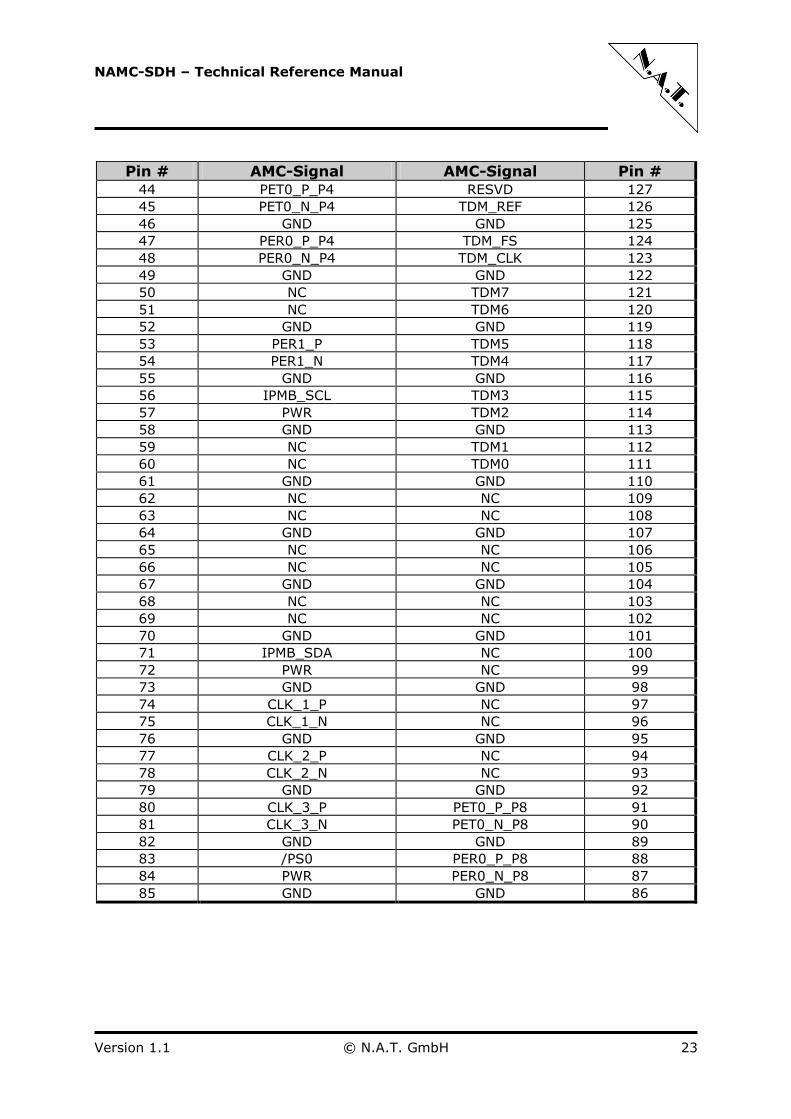
NAMC-SDH – Technical Reference Manual
Version 1.1 © N.A.T. GmbH 23
Pin # AMC-Signal AMC-Signal Pin # 44 PET0_P_P4 RESVD 127
45 PET0_N_P4 TDM_REF 126
46 GND GND 125
47 PER0_P_P4 TDM_FS 124
48 PER0_N_P4 TDM_CLK 123
49 GND GND 122
50 NC TDM7 121
51 NC TDM6 120
52 GND GND 119
53 PER1_P TDM5 118
54 PER1_N TDM4 117
55 GND GND 116
56 IPMB_SCL TDM3 115
57 PWR TDM2 114
58 GND GND 113
59 NC TDM1 112
60 NC TDM0 111
61 GND GND 110
62 NC NC 109
63 NC NC 108
64 GND GND 107
65 NC NC 106
66 NC NC 105
67 GND GND 104
68 NC NC 103
69 NC NC 102
70 GND GND 101
71 IPMB_SDA NC 100
72 PWR NC 99
73 GND GND 98
74 CLK_1_P NC 97
75 CLK_1_N NC 96
76 GND GND 95
77 CLK_2_P NC 94
78 CLK_2_N NC 93
79 GND GND 92
80 CLK_3_P PET0_P_P8 91
81 CLK_3_N PET0_N_P8 90
82 GND GND 89
83 /PS0 PER0_P_P8 88
84 PWR PER0_N_P8 87
85 GND GND 86

NAMC-SDH – Technical Reference Manual
Version 1.1 © N.A.T. GmbH 24
4.3.2 JP1: Atmel Programming Header
Connector JP1 connects to the programming-port of the Atmel µC device.
Table 7: JP1: Atmel Programming Header – Pin Assignment
Pin # Signal Signal Pin # 1 PDI_DATA +3.3V 2
3 nc /PROG_ENABLE* 4
5 PDI_CLK GND 6 * For programming the NAMC-SDH out of system, connect PIN4 and PIN6 to force PIN4 to Low-Status.
4.3.3 J1-J4: Front Panel SFP Connectors
The optical front panel connectors J1-J4 have standard LC-plugs and can be
equipped with either singlemode or multimode transceivers.
Table 8: J1: Front Panel SFP Connector – Pin Assignment
Pin # Signal Signal Pin # 1 GND nc 2
3 GND SDA_SFP1 4
5 SCL_SFP1 +3.3V_SFP1 6
7 +3.3V_SFP1 TMX_LOSW1 8
9 GND GND 10
11 GND TMX_RXW1_N 12
13 TMX_RXW1_P GND 14
15 +3.3V_SFP1 +3.3V_SFP1 16
17 GND TMX_TXW1_P 18
19 TMX_TXW1_N GND 20
Table 9: J2: Front Panel SFP Connector – Pin Assignment
Pin # Signal Signal Pin # 1 GND nc 2
3 GND SDA_SFP2 4
5 SCL_SFP2 +3.3V_SFP2 6
7 +3.3V_SFP2 TMX_LOSW2 8
9 GND GND 10
11 GND TMX_RXW2_N 12
13 TMX_RXW2_P GND 14
15 +3.3V_SFP2 +3.3V_SFP2 16
17 GND TMX_TXW2_P 18
19 TMX_TXW2_N GND 20

NAMC-SDH – Technical Reference Manual
Version 1.1 © N.A.T. GmbH 25
Table 10: J3: Front Panel SFP Connector – Pin Assignment
Pin # Signal Signal Pin # 1 GND nc 2
3 GND SDA_SFP3 4
5 SCL_SFP3 +3.3V_SFP3 6
7 +3.3V_SFP3 TMX_LOSW3 8
9 GND GND 10
11 GND TMX_RX3_MUX_N 12
13 TMX_RX3_MUX_P GND 14
15 +3.3V_SFP3 +3.3V_SFP3 16
17 GND TMX_TX3_MUX_P 18
19 TMX_TX3_MUX_N GND 20
Table 11: J4: Front Panel SFP Connector – Pin Assignment
Pin # Signal Signal Pin # 1 GND nc 2
3 GND SDA_SFP4 4
5 SCL_SFP4 +3.3V_SFP4 6
7 +3.3V_SFP4 TMX_LOSW4 8
9 GND GND 10
11 GND TMX_RX4_MUX_N 12
13 TMX_RX4_MUX_P GND 14
15 +3.3V_SFP4 +3.3V_SFP4 16
17 GND TMX_TX4_MUX_P 18
19 TMX_TX4_MUX_N GND 20
4.3.4 SW1: Hot Swap Switch
Switch SW1 is used to support Hot-Swapping of the module. It conforms to PICMG
AMC.0.
4.3.5 DIP SW2: Ethernet Options Select
The table below gives an overview of the operating parameters configurable via
DIP SW2. Details are given in the following subchapters.
Table 12: DIP SW2 – Pin-Assignment – Overview
Switch # Function 1 LIF Operation Mode Select
2 Backplane Ethernet Select
3 Fat Pipe Select
4 MAC-Address Value Bit 0
5 MAC-Address Value Bit 1
6 External Memory Reset
7 Ethernet Auto-Negotiation Disable
8 MAC-Address Configuration

NAMC-SDH – Technical Reference Manual
Version 1.1 © N.A.T. GmbH 26
4.3.5.1 DIP SW2: Switch 1 – LIF Operation Mode Select
By operating switch1 of DIP SW2 the LIF Operation Mode can be selected
according to the following table.
Table 13: DIP SW2: Switch 1 – LIF Operation Mode Select
DIP SW2 – Switch 1 Function
LIF Operation Mode:
2x working/2x protect
LIF Operation Mode:
4x working
Default:
Switch 1 of DIP SW2 is toggled to OFF, LIF Operation Mode 4x working is selected.
4.3.5.2 DIP SW2: Switch 2 – Backplane Ethernet Select
By operating switch 2 of DIP SW2 the Ethernet Port Mapping can be selected.
Table 14: DIP SW2: Switch 2 – Backplane Ethernet Select
DIP SW2 – Switch 2 Function
Ethernet via Port 1/8
Ethernet via Port 0/4
Default:
Switch 2 of DIP SW2 is toggled to OFF, Ethernet via Port 0/4 is selected.

NAMC-SDH – Technical Reference Manual
Version 1.1 © N.A.T. GmbH 27
4.3.5.3 DIP SW2: Switch 3 – Fat Pipe Select
By operating switch 3 of DIP SW2 the Fat Pipe Mapping can be selected.
Table 15: DIP SW2: Switch 3 – Fat Pipe Select
DIP SW2 – Switch 3 Function
Ethernet via Port 4/8
Ethernet via Port 0/1
Default:
Switch 3 of DIP SW2 is toggled to OFF, Ethernet via Port 0/1 is selected.
4.3.5.4 DIP SW2: Switch 4 – MAC-Address Value Bit 0
By operating switch 4 of DIP SW2 the MAC-Address Value of Bit 0 can be selected.
Note: This selection is valid only if switch 8 of DIP SW2 is turned to “ON”.
Table 16: DIP SW2: Switch 4 – MAC-Address Value Bit 0
DIP SW2 – Switch 4 Function
MAC-Address Value of Bit 0 is set to “1”
MAC-Address Value of Bit 0 is set to “0”
Default:
Switch 4 of DIP SW2 is toggled to OFF, MAC-Address Value of Bit 0 is set to “0”.

NAMC-SDH – Technical Reference Manual
Version 1.1 © N.A.T. GmbH 28
4.3.5.5 DIP SW2: Switch 5 – MAC-Address Value Bit 1
By operating switch 5 of DIP SW2 the MAC-Address value of Bit 1 can be selected.
Note: This selection is valid only if switch 8 of DIP SW2 is turned to “ON”.
Table 17: DIP SW2: Switch 5 – MAC-Address Value Bit 1
DIP SW2 – Switch 5 Function
MAC-Address value of Bit 1 is set to “1”
MAC-Address value of Bit 1 is set to “0”
Default:
Switch 5 of DIP SW2 is toggled to OFF, MAC-Address value of Bit 1 is set to “0”.
4.3.5.6 DIP SW2: Switch 6 – External Memory Reset
By operating switch 6 of DIP SW2 permanent reset of the external memory can be
enabled.
Table 18: DIP SW2: Switch 6 – External Memory Reset
DIP SW2 – Switch 6 Function
Permanent reset of external memory is
enabled
Permanent reset of external memory is
disabled
Default:
Switch 6 of DIP SW2 is toggled to OFF, permanent reset of external memory is
disabled.

NAMC-SDH – Technical Reference Manual
Version 1.1 © N.A.T. GmbH 29
4.3.5.7 DIP SW2: Switch 7 – Ethernet Auto-Negotiation
By operating switch 7 of DIP SW2 the Ethernet Auto-Negotiation can be disabled.
Note: For operation with the XAUI switch, turn this switch to “1”.
Table 19: DIP SW2: Switch 7 – External Memory Reset
DIP SW2 – Switch 7 Function
Ethernet Auto-Negotiation is disabled
Ethernet Auto-Negotiation is enabled
Default:
Switch 7 of DIP SW2 is toggled to OFF, Ethernet Auto-Negotiation is enabled.
4.3.5.8 DIP SW2: Switch 8 – MAC-Address Configuration
By operating switch 8 of DIP SW2 the MAC-Address Configuration can be enabled.
Note: The MAC-Address value is determined by switches 4/5 of DIP SW2.
Table 20: DIP SW2: Switch 8 – MAC-Address Configuration
DIP SW2 – Switch 8 Function
MAC-Address Configuration is enabled
MAC-Address Configuration is disabled
Default:
Switch 8 of DIP SW2 is toggled to OFF, MAC-Address Configuration is disabled.

NAMC-SDH – Technical Reference Manual
Version 1.1 © N.A.T. GmbH 30
5 NAMC-SDH Programming Notes
The FPGA on the NAMC-SDH implements various logical blocks. The table below shows
the memory map for the logical sub-blocks of the design. Refer to the following sub-
chapters for detailed information.
All devices shown in this memory map can be accessed via the so called Ethernet Control
Interface. This Interface uses a N.A.T. proprietary protocol based on Layer2 Ethernet
frames to perform memory mapped accesses via Ethernet. Please refer to the Ethernet
Control Interface Technical Reference Manual for further information (Appendix A, [7]).
The MAC address of the NAMC-SDH is built with the following scheme:
00:40:42:24:XX:XX with XXXX being the boards serial number in hexadecimal
representation
Table 21: FPGA Memory Map
Address Offset Logical Block 0x0000000 General Purpose Status (Read Only)
0x0000100 General Purpose Registers (Read/Write)
0x0000200 Heartbeat Time-Out Counter
0x0001000 SPI-Interface to FPGA EEPROM
0x0002000 SPI-Interface to PLL
0x0010000 Ethernet Matrix
0x0020000 Local Bus to Arrow / TEMUX
0x0040000 GbE-Block
0x0080000 iTDM-Block
0x0100000 SBI TSI-Block
0x0200000 HDLC-Decoder Block
0x0300000 HDLC-Encoder Block
0x0400000 Test-Logic Block
The following chapters give detailed information on the General Purpose Status Registers
(Read Only) and the General Purpose Registers (Read/Write). For further information
regarding the other registers, please refer to the NAMC-SDH Programming Manual
(Appendix A, [8]).

NAMC-SDH – Technical Reference Manual
Version 1.1 © N.A.T. GmbH 31
Table 22: FPGA Register Description – Overview
General Purpose – Read Only – 16 bit
0x0000000 FUNC_TYPE/PCB_VERS
0x0000002 FPGA_VERS
0x0000004 MAGIC_VAL_1
0x0000006 MAGIC_VAL_2
0x0000008 BOARD_ID
0x000000A INIT_CALIB
0x000000C IRQ-Status
0x000000E AUTO_RD_BYTES
0x0000010 CARRIER_ID/GEO_ADDRESS
0x0000012 ATMEL_EXT_INFO
0x0000014 DIP_SW_STAT
General Purpose – Read/Write – 16 bit
0x0000100 RESET
0x0000102 SFP_LED_CTRL
0x0000104 AMC_LED_CTRL
0x0000106 PLL_155_CLKSEL
0x000010A SBI_CTRL
0x000010C IRQ_EN
0x000010E TCLK_CTRL
0x000011E BOARD_INIT_STAT

NAMC-SDH – Technical Reference Manual
Version 1.1 © N.A.T. GmbH 32
5.1.1 0x0000000 – FUNC_TYPE/PCB_VERS
Bit Name Description Default Access
15..8 FUNC_TYPE Identifies optional FPGA functionality
0x5: bi-directional HDLC-Controller
Read
Only
7..4 PCB_MAJ_VERS PCB Major Version (x.y)
4 bit unsigned number
HW init Read
Only
3..0 PCB_MIN_VER PCB Minor Version (x.y)
4 bit unsigned number
HW init Read
Only
Note: The PCB Version is determined by the level of unused pins hardcoded on
the PCB.
5.1.2 0x0000002 – FPGA_VERS
Bit Name Description Default Access
15..8 FPGA_SUB_VERS FPGA Sub Version (x.y.z);
8 bit unsigned number
n/a Read
Only
7..4 FPGA_MAJ_VERS FPGA Major Version (x.y.z)
4 bit unsigned number
n/a Read
Only
3..0 FPGA_MIN_VERS FPGA Minor Version (x.y.z)
4 bit unsigned number
n/a Read
Only
5.1.3 0x0000004 – MAGIC_VAL_1
This read-only register can be used by the device driver to probe register access.
Bit Name Description Default Access
15..0 MAGIC_VAL_1 Testing purposes 0xAA55 Read
Only
5.1.4 0x0000006 – MAGIC_VAL_2
This read-only register can be used by the device driver to probe register access.
Bit Name Description Default Access
15..0 MAGIC_VAL_2 Testing purposes 0xDEAD Read
Only

NAMC-SDH – Technical Reference Manual
Version 1.1 © N.A.T. GmbH 33
5.1.5 0x0000008 – BOARD_ID
This read-only register can be used by the device driver to probe register access.
It holds the N.A.T. internal board-ID of the NAMC-SDH.
Bit Name Description Default Access
15..0 BOARD_ID Internal board-ID 0x0B31 Read
Only
5.1.6 0x000000A – INIT/CALIB
Bits [11.8] within this register reflect the Link Status of Ethernet Ports 0/1/4/8.
Bits [5..3] within this register show the logical value of the PLL status outputs.
Bits [2..0] within this register show the status of the external memory self-test.
Please refer to the DS31400 manual for detailed information.
Bit Name Description Default Access
15..12 Reserved na Read
Only
11 ETH_P8_STAT Link Status Ethernet Port 8 na Read
Only
10 ETH_P4_STAT Link Status Ethernet Port 4 na Read
Only
9 ETH_P1_STAT Link Status Ethernet Port 1 na Read
Only
8 ETH_P0_STAT Link Status Ethernet Port 0 na Read
Only
7..6 Reserved na Read
Only
5 PLL_SRFAIL PLL SR failed na Read
Only
4 PLL_LOCKED PLL locked na Read
Only
3 PLL_155_LOCKED PLL 155 MHz locked na Read
Only
2 DDR_INIT Initialisation / Calibration of DDR3-
RAM complete
1 Read
Only
1 QDR2_INIT Initialisation / Calibration of QDR+-
RAM complete
1 Read
Only
0 QDR1_INIT Initialisation / Calibration of QDR+-
RAM complete
1 Read
Only

NAMC-SDH – Technical Reference Manual
Version 1.1 © N.A.T. GmbH 34
5.1.7 0x000000C – IRQ_STAT
This register displays the interrupt status line of all interrupt capable devices on
the NAMC-SDH. A value of ‘1’ means that the respective interrupt is pending. An
IRQ transmitted via ECI (Ethernet Control Interface) is acknowledged and re-
armed by writing a ‘1’ to the corresponding bit.
Bit Name Description Default Access
15..0 IRQ_STAT Interrupt Status 0x0000 Read
Only
5.1.8 0x000000E – AUTO_RD_BYTES
This register displays the serial number of the board read from the FPGA
configuration memory.
Bit Name Description Default Access
15..8 AUTO_RD_BYTES_1 AUTO_RD_BYTES_1 0x00 Read
Only
7..0 AUTO_RD_BYTES_0 AUTO_RD_BYTES_0 0x00 Read
Only
5.1.9 0x0000010 – CARRIER_ID/GEO_ADDRESS
Bit Name Description Default Access
15..8 CARRIER_ID Carrier Manager ID
0x80 + 2*Carrier Number
0x00 Read
Only
7..0 GEO_ADDRESS Geographical Address (Slot ID)
0x72: AMC1
0x74: AMC2
0x76: AMC3
0x78: AMC4
0x7A: AMC5
0x7C: AMC6
0x7E: AMC7
0x80: AMC8
0x82: AMC9
0x84: AMC10
0x86: AMC11
0x88: AMC12
na Read
Only

NAMC-SDH – Technical Reference Manual
Version 1.1 © N.A.T. GmbH 35
5.1.10 0x0000012 – ATMEL_EXT_INFO
Bit Name Description Default Access
15..0 Reserved 0x0000 Read
Only
5.1.11 0x0000014 – DIP_SW_STAT
If a switch of DIP SW2 is set to ‘ON’, the corresponding bit is set to ‘0’; if the
switch is turned to ‘OFF’, the bit is set to ‘1’.
Bit Name Description Default Access
15..8 Reserved 0x00 Read
Only
7 DIP_SW8_STAT Reflects DIP SW2 – Switch 8
status: MAC-Address Configuration
HW init Read
Only
6 DIP_SW7_STAT Reflects DIP SW2 – Switch 7
status: Ethernet Auto-Negotiation
Disable
HW init Read
Only
5 DIP_SW6_STAT Reflects DIP SW2 – Switch 6
status: External Memory Reset
HW init Read
Only
4 DIP_SW5_STAT Reflects DIP SW2 – Switch 5
status: MAC-Address Value Bit 1
HW init Read
Only
3 DIP_SW4_STAT Reflects DIP SW2 – Switch 4
status: MAC-Address Value Bit 0
HW init Read
Only
2 DIP_SW3_STAT Reflects DIP SW2 – Switch 3
status: Fat Pipe Select
HW init Read
Only
1 DIP_SW2_STAT Reflects DIP SW2 – Switch 2
status: Backplane Ethernet Select
HW init Read
Only
0 DIP_SW1_STAT Reflects DIP SW2 – Switch 1
status: LIF Operation Mode Select
HW init Read
Only
NAMC-SDH – Technical Reference Manual
Version 1.1 © N.A.T. GmbH 36
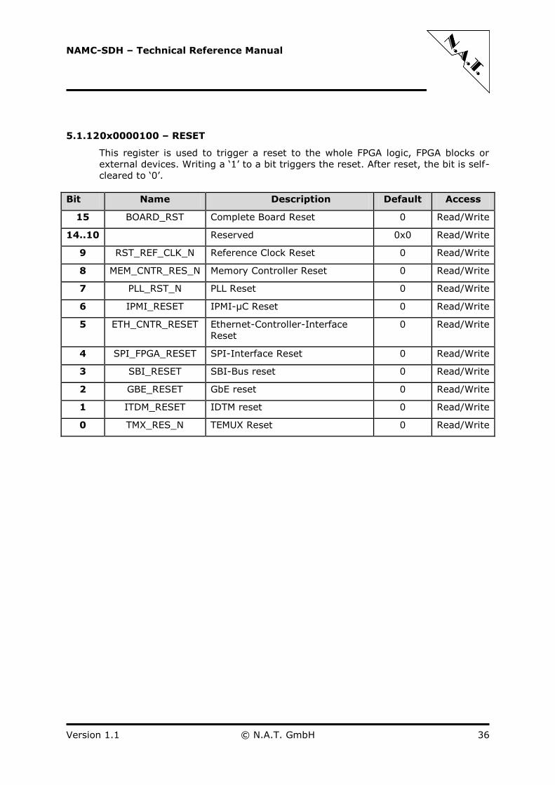
5.1.12 0x0000100 – RESET
This register is used to trigger a reset to the whole FPGA logic, FPGA blocks or
external devices. Writing a ‘1’ to a bit triggers the reset. After reset, the bit is self-
cleared to ‘0’.
Bit Name Description Default Access
15 BOARD_RST Complete Board Reset 0 Read/Write
14..10 Reserved 0x0 Read/Write
9 RST_REF_CLK_N Reference Clock Reset 0 Read/Write
8 MEM_CNTR_RES_N Memory Controller Reset 0 Read/Write
7 PLL_RST_N PLL Reset 0 Read/Write
6 IPMI_RESET IPMI-µC Reset 0 Read/Write
5 ETH_CNTR_RESET Ethernet-Controller-Interface
Reset
0 Read/Write
4 SPI_FPGA_RESET SPI-Interface Reset 0 Read/Write
3 SBI_RESET SBI-Bus reset 0 Read/Write
2 GBE_RESET GbE reset 0 Read/Write
1 ITDM_RESET IDTM reset 0 Read/Write
0 TMX_RES_N TEMUX Reset 0 Read/Write

NAMC-SDH – Technical Reference Manual
Version 1.1 © N.A.T. GmbH 37
5.1.13 0x0000102 – SFP_LED_CTRL
This register is used to control the four SFP interface status LEDs on the AMC
module’s front panel above the optical connectors. The LEDs can be configured to
the functionality listed below:
Bit Name Description Default Access
15..12 SFP_LED4 0x0 off
0x1 green solid on
0x2 red solid on
0x3 green slow blink
0x4 red slow blink
0x5 green fast blink
0x6 red fast blink
0x7 green fast double flashing
0x8 red fast double flashing
0x9 orange solid on
0xA orange slow blink
0xB orange fast blink
0xC orange fast double flashing
0xD green/red alternate slow blink
0xE green/red alternate fast blink
0xF running light
0x0 Read/Write
11..8 SFP_LED3 0x0 Read/Write
7..4 SFP_LED2 0x0 Read/Write
3..0 SFP_LED1 0x0 Read/Write
5.1.14 0x0000106 – PLL_155_CLKSEL
Setting PLL_155_CLKSEL to ‘1’ causes the Temux336 155MHz reference clock to
be sourced by a local 77.76 MHz oscillator instead coming from the DS31400 PLL.
Bit Name Description Default Access
15..1 Reserved 0x000 Read/Write
0 PLL_155_CLKSEL PLL 155 MHz Clock Select 0 Read/Write
NAMC-SDH – Technical Reference Manual
Version 1.1 © N.A.T. GmbH 38
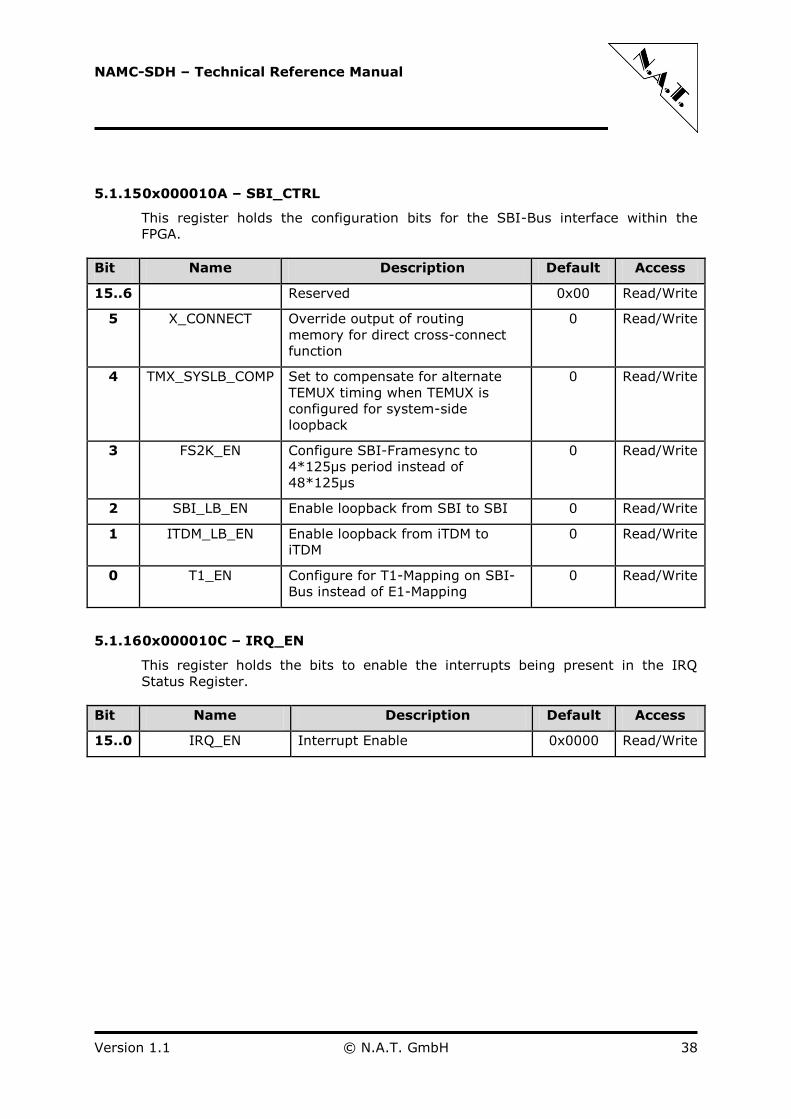
5.1.15 0x000010A – SBI_CTRL
This register holds the configuration bits for the SBI-Bus interface within the
FPGA.
Bit Name Description Default Access
15..6 Reserved 0x00 Read/Write
5 X_CONNECT Override output of routing
memory for direct cross-connect
function
0 Read/Write
4 TMX_SYSLB_COMP Set to compensate for alternate
TEMUX timing when TEMUX is
configured for system-side
loopback
0 Read/Write
3 FS2K_EN Configure SBI-Framesync to
4*125µs period instead of
48*125µs
0 Read/Write
2 SBI_LB_EN Enable loopback from SBI to SBI 0 Read/Write
1 ITDM_LB_EN Enable loopback from iTDM to
iTDM
0 Read/Write
0 T1_EN Configure for T1-Mapping on SBI-
Bus instead of E1-Mapping
0 Read/Write
5.1.16 0x000010C – IRQ_EN
This register holds the bits to enable the interrupts being present in the IRQ
Status Register.
Bit Name Description Default Access
15..0 IRQ_EN Interrupt Enable 0x0000 Read/Write
NAMC-SDH – Technical Reference Manual
Version 1.1 © N.A.T. GmbH 39
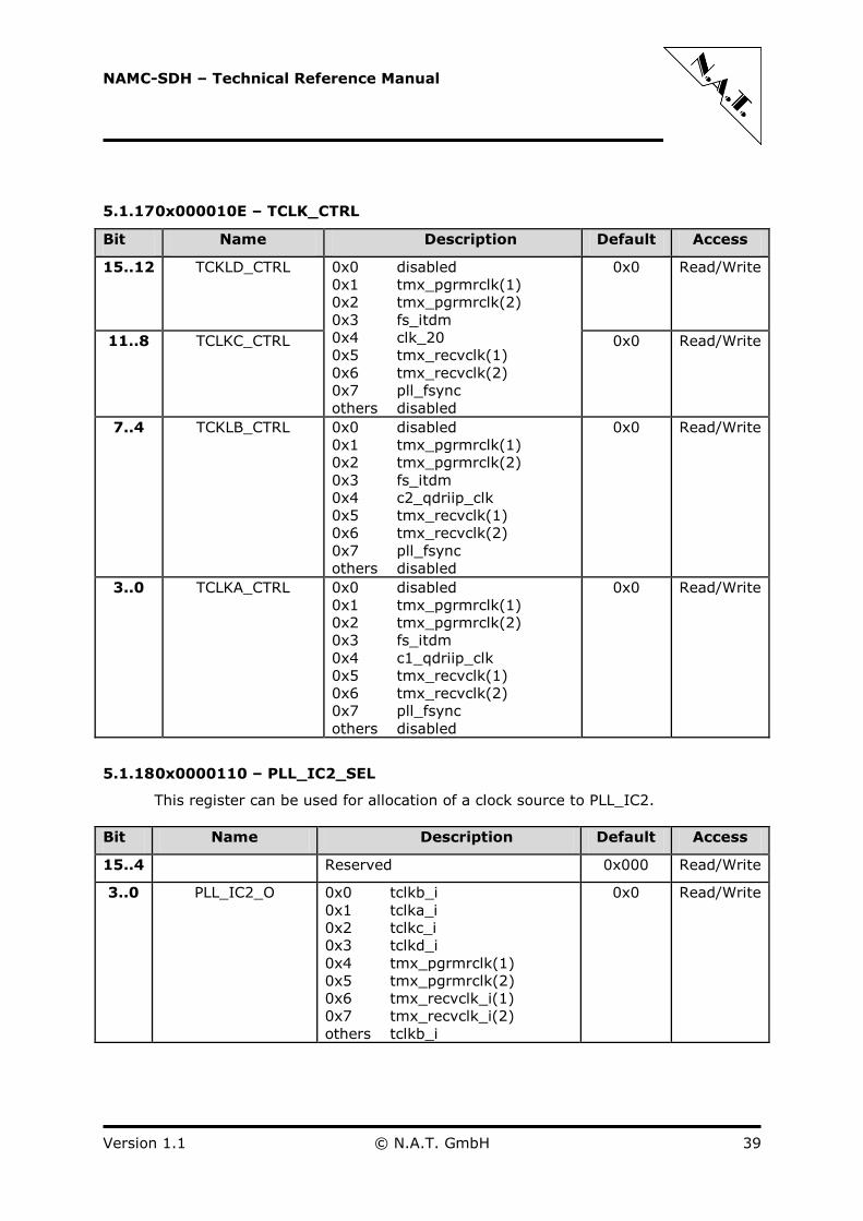
5.1.17 0x000010E – TCLK_CTRL
Bit Name Description Default Access
15..12 TCKLD_CTRL 0x0 disabled
0x1 tmx_pgrmrclk(1)
0x2 tmx_pgrmrclk(2)
0x3 fs_itdm
0x4 clk_20
0x5 tmx_recvclk(1)
0x6 tmx_recvclk(2)
0x7 pll_fsync
others disabled
0x0 Read/Write
11..8 TCLKC_CTRL 0x0 Read/Write
7..4 TCKLB_CTRL 0x0 disabled
0x1 tmx_pgrmrclk(1)
0x2 tmx_pgrmrclk(2)
0x3 fs_itdm
0x4 c2_qdriip_clk
0x5 tmx_recvclk(1)
0x6 tmx_recvclk(2)
0x7 pll_fsync
others disabled
0x0 Read/Write
3..0 TCLKA_CTRL 0x0 disabled
0x1 tmx_pgrmrclk(1)
0x2 tmx_pgrmrclk(2)
0x3 fs_itdm
0x4 c1_qdriip_clk
0x5 tmx_recvclk(1)
0x6 tmx_recvclk(2)
0x7 pll_fsync
others disabled
0x0 Read/Write
5.1.18 0x0000110 – PLL_IC2_SEL
This register can be used for allocation of a clock source to PLL_IC2.
Bit Name Description Default Access
15..4 Reserved 0x000 Read/Write
3..0 PLL_IC2_O 0x0 tclkb_i
0x1 tclka_i
0x2 tclkc_i
0x3 tclkd_i
0x4 tmx_pgrmrclk(1)
0x5 tmx_pgrmrclk(2)
0x6 tmx_recvclk_i(1)
0x7 tmx_recvclk_i(2)
others tclkb_i
0x0 Read/Write

NAMC-SDH – Technical Reference Manual
Version 1.1 © N.A.T. GmbH 40
5.1.19 0x000011E – BOARD_INIT_STAT
This register can be used by driver software to store a value that indicates
whether the board has been fully initialized or not.
Bit Name Description Default Access
15..0 BOARD_INIT_STAT Holds initialization status of the
board
0x0000 Read/Write
NAMC-SDH – Technical Reference Manual
Version 1.1 © N.A.T. GmbH 41
5.2 FPGA GbE/ITDM Configuration
For configuration and programming of the GbE/ITDM block please refer to the N.A.T.
driver code and the ITDM-FPGA Manual (Appendix A, [4], NDA required).
The ITDM Channel-ID for a certain E1 timeslot is calculated the following way:
ch_id = (E1_TS# * 63 + E1#) * 4 + STM#
If the SBI-bus logic is configured for T1 mode, the Channel-ID for a certain T1 timeslot is
calculated this way:
ch_id = (T1_TS# * 84 + T1#) * 4 + STM#
Table 23: SBI-Bus Timeslot Parameter
Parameter Function E1# Number of the E1 Link; Ranging from 0 to 62
T1# Number of the T1 Link; Ranging from 0 to 83
E1_TS# Number of the Timeslot within a E1 Link;
Ranging from 0 to 31
T1_TS# Number of the Timeslot within a T1 Link;
Ranging from 0 to 23
STM# Number of the four byte interleaved STM1 links
present on the SBI-bus; Ranging from 0 to 3

NAMC-SDH – Technical Reference Manual
Version 1.1 © N.A.T. GmbH 42
6 Board Specification
Table 24: NAMC-SDH Features - Overview
FPGA XILINX Kintex 7 (default: XC7K325T)
AMC-Module Standard Advanced Mezzanine Card
single width, mid-size
Front-I/O Four optical 155/622Mbps OC-3/12 STM-1 line
interfaces
Power Consumption 12V / 2A
Operating Temperature 0°C – +55°C with forced cooling
Storage Temperature -40°C - +85°C
Humidity 10% – 90% rh non-condensing
Standards compliance PICMG AMC.0 Rev. 2.0
PICMG SFP.0 Rev. 1.0 (System Fabric Plane Format)
PICMG SFP.1 Rev. 1.0 (Internal TDM)
IPMI Specification v2.0 Rev. 1.0
PICMG µTCA.0 Rev. 1.0

NAMC-SDH – Technical Reference Manual
Version 1.1 © N.A.T. GmbH 43
7 Installation
7.1 Safety Note
To ensure proper functioning of the NAMC-SDH during its usual lifetime take the
following precautions before handling the board.
CAUTION
Electrostatic discharge and incorrect board installation and uninstallation can damage
circuits or shorten their lifetime!
Before installing or uninstalling the NAMC-SDH read this installation section
Before installing or uninstalling the NAMC-SDH, read the Installation Guide and the
User’s Manual of the carrier board used, or of the µTCA system the board will be
plugged into.
Before installing or uninstalling the NAMC-SDH on a carrier board or both in a rack:
Check all installed boards and modules for steps that you have to take before
turning on or off the power.
Take those steps
Finally turn on or off the power if necessary.
Make sure the part to be installed / removed is hot swap capable, if you don’t
switch off the power.
Before touching integrated circuits ensure to take all require precautions for handling
electrostatic devices.
Ensure that the NAMC-SDH is connected to the carrier board or to the µTCA
backplane with the connector completely inserted.
When operating the board in areas of strong electromagnetic radiation ensure that the
module
is bolted the front panel or rack
and shielded by closed housing

NAMC-SDH – Technical Reference Manual
Version 1.1 © N.A.T. GmbH 44
7.2 Installation Prerequisites and Requirements
IMPORTANT
Before powering up check this section for installation prerequisites and requirements!
7.2.1 Requirements
The installation requires only
an ATCA carrier board, or a µTCA backplane for connecting the NAMC-SDH
power supply
cooling devices
7.2.2 Power supply
The power supply for the NAMC-SDH must meet the following specifications:
required for the module:
+12V / 2A max.
+ 3,3V / 0.15A max.
7.2.3 Automatic Power Up
In the following situations the NAMC-SDH will automatically be reset and proceed
with a normal power up:
The voltage sensor generates a reset
when +12V voltage level drops below 8V
when +3.3V voltage level drops below 3.08V
The carrier board / backplane signals a PCIe Reset.

NAMC-SDH – Technical Reference Manual
Version 1.1 © N.A.T. GmbH 45
7.3 Statement on Environmental Protection
7.3.1 Compliance to RoHS Directive
Directive 2011/65/EU of the European Parliament and of the Council of 8 June
2011 on the "Restriction of the use of certain Hazardous Substances in Electrical
and Electronic Equipment" (RoHS) predicts that all electrical and electronic
equipment being put on the European market after June 30th, 2006 must contain
lead, mercury, hexavalent chromium, polybrominated biphenyls (PBB) and poly-
brominated diphenyl ethers (PBDE) and cadmium in maximum concentration
values of 0.1% respective 0.01% by weight in homogenous materials only.
As these hazardous substances are currently used with semiconductors, plastics
(i.e. semiconductor packages, connectors) and soldering tin any hardware product
is affected by the RoHS directive if it does not belong to one of the groups of
products exempted from the RoHS directive.
Although many of hardware products of N.A.T. are exempted from the RoHS
directive it is a declared policy of N.A.T. to provide all products fully compliant to
the RoHS directive as soon as possible. For this purpose since January 31st, 2005
N.A.T. is requesting RoHS compliant deliveries from its suppliers. Special attention
and care has been paid to the production cycle, so that wherever and whenever
possible RoHS components are used with N.A.T. hardware products already.
7.3.2 Compliance to WEEE Directive
Directive 2002/95/EC of the European Commission on "Waste Electrical and
Electronic Equipment" (WEEE) predicts that every manufacturer of electrical and
electronical equipment which is put on the European market has to contribute to
the reuse, recycling and other forms of recovery of such waste so as to reduce
disposal. Moreover this directive refers to the Directive 2002/95/EC of the
European Commission on the "Restriction of the use of certain Hazardous
Substances in Electrical and Electronic Equipment" (RoHS).
Having its main focus on private persons and households using such electrical and
electronic equipment the directive also affects business-to-business relationships.
The directive is quite restrictive on how such waste of private persons and
households has to be handled by the supplier/manufacturer; however, it allows a
greater flexibility in business-to-business relationships. This pays tribute to the
fact with industrial use electrical and electronical products are commonly
integrated into larger and more complex environments or systems that cannot
easily be split up again when it comes to their disposal at the end of their life
cycles.
As N.A.T. products are solely sold to industrial customers, by special arrangement
at time of purchase the customer agreed to take the responsibility for a WEEE
compliant disposal of the used N.A.T. product. Moreover, all N.A.T. products are
marked according to the directive with a crossed out bin to indicate that these
products within the European Community must not be disposed with regular
waste.
NAMC-SDH – Technical Reference Manual
Version 1.1 © N.A.T. GmbH 46
If you have any questions on the policy of N.A.T. regarding the Directive
2011/65/EU of the European Parliament and of the Council of 8 June 2011 on the
"Restriction of the use of certain Hazardous Substances in Electrical and Electronic
Equipment" (RoHS) or the Directive 2002/95/EC of the European Commission on
"Waste Electrical and Electronic Equipment" (WEEE) please contact N.A.T. by
phone or e-mail.
7.3.3 Compliance to CE Directive
Compliance to the CE directive is declared. A ‘CE’ sign can be found on the PCB.
7.3.4 Product Safety
The board complies with EN60950 and UL1950.
7.3.5 Compliance to REACH
The REACH EU regulation (Regulation (EC) No 1907/2006) is known to N.A.T.
GmbH. N.A.T. did not receive information from their European suppliers of
substances of very high concern of the ECHA candidate list. Article 7(2) of REACH
is notable as no substances are intentionally being released by NAT products and
as no hazardous substances are contained. Information remains in effect or will be
otherwise stated immediately to our customers.
NAMC-SDH – Technical Reference Manual
Version 1.1 © N.A.T. GmbH 47
8 Known Bugs / Restrictions
none

NAMC-SDH – Technical Reference Manual
Version 1.1 © N.A.T. GmbH 48
Appendix A: Reference Documentation [1] Atmel, Atmega48/88/168/V Product Data, Rev. 2545G, 06/06
[2] Zarlink, DS31400 PLL Data Sheet 04/2012
[3] Traco Power DC/DC Converters, TOS Series, POL Converter, Rev. 10/05
[4] N.A.T.: ITDM-FPGA Technical Reference Manual, October 2006, Ver. 1.0
[5] PMC Sierra TEMUX336, PMC-2061563, Issue 4 (November 2008)
[6] Xilinx Kintex 7 FPGA DS182 (v2.5) October 4, 2013
[7] N.A.T.: Ethernet Control Interface Technical Reference Manual, Ver. 1.0, Dez 2007
[8] N.A.T.: NAMC-SDH Programming Manual, Ver. 1.0, Jun 2014

NAMC-SDH – Technical Reference Manual
Version 1.1 © N.A.T. GmbH 49
Appendix B: Document’s History
Revision Date Description Author 1.0 24.06.2014 initial release se
1.1 11.08.2014 Updated Chapter 5.1.12 -
Register 0x0000100 – RESET
se
3.09.2014 Added Chapter 5.1.18 -
0x0000110 – PLL_IC2_SEL
se
10.09.2014 Added chapter 3.1.7 – Clock Connectivity se
25.11.2014 Corrected form factor to mid-size
Added photo (Figure 1)
Te
se