nano- and micro-structures for organic/hybrid photonics
TRANSCRIPT

Nano- and Micro-structures for
organic/hybrid photonics and optoelectronics
Valentina Robbiano
A dissertation submitted for the degree of Doctor of Philosophy
Department of Physics and Astronomy and London Centre for
Nanotechnology
University College London
London, December 2016
LONDON’S GLOBAL UNIVERSITY

[1]
I, Valentina Robbiano, confirm that the work presented in this thesis is my own. Where
information has been derived from other sources and work which has formed part of jointly-
authored publications has been used I confirm that this has been indicated in the thesis.
Supervisor: Prof. Franco Cacialli,
Department of Physics and Astronomy and London Centre for Nanotechnology, University
College London
Second Supervisor: Dr. Ioannis Papakostantinou
Department of Electronic and Electrical Engineering, University College London

[2]
Acknowledgments
My research was funded by the European Commission Seventh Framework Program
(FP7/2007-2013) Marie Curie Initial Training Network CONTEST under Grant agreement
PITN-GA-2012-317488.
First I would like to thank Prof. Franco Cacialli for giving me the opportunity to work
on this interesting project and for the guidance throughout my PhD. I would also like to
acknowledge Dr. Ioannis Papakostantinou, my second supervisor, for his valuable input during
the transfer viva and for the constructive feedbacks on this dissertation.
Another big thanks goes to the external collaborators that helped me a lot during these
three years and to all the members of the CONTEST project. In particular, Prof. Paolo Lugli,
Simone Colasanti, Engin Cagatay and Alaa Abdellah from TUM, for being so welcoming with
me during my secondment there and for the good work done together; Prof. Giuseppe Barillaro,
Lucanos Strambini and Salvatore Surdo from UNIPI, for letting me get in touch with the
interesting world of silicon photonics, and Prof. Davide Comoretto from UNIGE, for the
constant help in whatever is related to photonics.
The biggest thank goes to all my colleagues: Luca Santarelli, Ludovica Intilla, Giuseppe
Paterno’, Alessandro Minotto, Andrea Zampetti, Giulia Tregnago, Nico Seidler, Keith Fraser,
Francesco Bausi, Giuseppe Carnicella, Tecla Arcidiacono and Gianfranco Cotella, to the MsC
students, and to everyone who has worked in the group: Emanuele Marino, Giovanni Polito,
Tiziana Fiore, Shimpei Goto, Martina Dianetti. I truly enjoyed my time with you at UCL. I
would also like to express my deep gratitude to Prof. Shabbir Mian (Apollo) for the help and all
the scientific stuff I learnt from him.
I thank my family for the support they give me every day of my life. This is dedicated
to all of you.
Last, but not least, I want to thank who has been wonderful with his continuous help
and support. Everything is perfect when you are by my side.
[3]
Abstract
In this work I present nano- and micro-patterning techniques useful especially in
photonics and optoelectronics. In fact, these structures give the possibility to tailor the
photophysical and electrical properties of organic and hybrid active materials, spanning from
well-known conjugated polymers, to organo-halaide perovskite that nowadays are gaining a lot
of interest due to their high performances in photovoltaic devices.
The first part is dedicated to the study of the optical properties of conjugated polymers
embedded/infiltrated into photonic crystals. In particular, I will show how it is possible to
prepare these composite materials and tune their optical properties. The preparation technique
has been improved, leading to a promising simple, widely available and low cost preparation of
both organic and hybrid photonic structures. The optical properties have been investigated via
both steady-state and time-resolved optical techniques. I believe that results obtained are a
valuable feedback for future application such as low-threshold optically pumped lasers.
In the second part, I will present the application of nanostructured layers in
optoelectronic devices. I will show how nanostructured architectures are used to obtain efficient
organo-halide perovskite solar cells. This nanostructure induced an increased light absorption
due to a controlled light scattering and a controlled microscopic morphology of perovskite
films, opening up a wide range of possible investigations, from charge transport optimization to
optical enhancements for photovoltaic, light emitting and lasing devices.
Finally, I’ve studied the preparation of nanostructured conductive thin films for flexible
transparent electrodes suitable for optoelectronic devices. Furthermore, I’ve observed that by
introducing a layer of a polyamine derivative it has been possible to tune the work function of
these electrodes, therefore changing (lowering) the injection barriers for charge at the interface
between the semiconductor and the electrode.

[4]
Contents
List of figures ................................................................................................................................. 6
List of tables ................................................................................................................................. 13
List of publications ...................................................................................................................... 14
Introduction ......................................................................................................... 16
Thesis overview ................................................................................................... 17
1 – Nano- and Micro-structures ........................................................................ 19
1.1 Photonic Crystals ............................................................................................................... 19
1.1.1 Photonic band formation ............................................................................................ 19
1.1.2 Scale Invariance of Maxwell’s equation .................................................................... 24
1.1.3 Bragg-Snell’s Law ..................................................................................................... 25
1.1.4 Density of states ......................................................................................................... 27
1.2 Transparent and conductive nanostructured thin films ..................................................... 29
1.2.1 CNTs .......................................................................................................................... 29
1.2.2 Metal nanostructures .................................................................................................. 31
1.3 Nano- micro-structuring techniques ................................................................................... 34
1.3.1 Top-down ................................................................................................................... 34
1.3.2 Bottom-up ................................................................................................................... 36
2 – Organic semiconductors and Organo-halide perovskite .......................... 37
2.1 Electric Properties .............................................................................................................. 37
2.1.1 Semiconducting behaviour and charge transport .................................................. 40
2.1.2 Work function ....................................................................................................... 41
2.2 Optical properties ............................................................................................................... 45
2.2.1 Photoluminescence properties and energy transfer ..................................................... 47
2.2.2 Time correlated single photon counting (TCSPC) ..................................................... 50
2.3 Organo-Lead Halide Perovskite ......................................................................................... 52
2.3.1 Perovskite-based photovoltaic devices ...................................................................... 53

[5]
3 – Polymer-silicon hybrid photonic structures ............................................... 58
3.1 Hybrid photonic structures for light emission ................................................................... 59
3.2 Experimental details ........................................................................................................... 61
3.3 Morphological characterization ........................................................................................ 63
3.4 Optical characterization .................................................................................................... 65
3.5 Conclusion ......................................................................................................................... 72
4 – Spectroscopy of synthetic opals ................................................................... 73
4.1 Synthetic opals .................................................................................................................. 73
4.2 Polyrotaxanes .................................................................................................................... 77
4.3 Experimental details .......................................................................................................... 78
4.4 Bare opals investigation .................................................................................................... 80
4.5 Infiltrated opals investigation ............................................................................................ 85
4.6 Conclusion ........................................................................................................................ 88
5 – Nanostructured titania for efficient perovskite solar cells ........................ 89
5.1 Nanostructures for optoelectronic ...................................................................................... 90
5.2 Experimental details ........................................................................................................... 91
5.3 Morphological and optical characterization ...................................................................... 93
5.4 Photovoltaic devices ......................................................................................................... 98
5.5 Conclusion ....................................................................................................................... 102
6 – Transparent electrodes: preparation, characterization and
work-function engineering ......................................................................... 103
6.1 Transparent conductive electrodes .................................................................................. 104
6.2 Experimental details ......................................................................................................... 105
6.3 Electrical and optical characterization ............................................................................ 107
6.4 Temperature behaviour ................................................................................................... 110
6.5 Work function engineering ............................................................................................. 113
6.6 Conclusion ....................................................................................................................... 116
Conclusion and Outlooks ................................................................................. 117
References .......................................................................................................... 119

[6]
List of figures
1.1 Schemes of 1D, 2D and 3D PhCs, Reproduced from ref. [16].
1.2 Dispersion relations for free electrons and inside a periodic potential (top) and for photons
in vacuum and inside a periodic dielectric (bottom), taken from ref. [3].
1.3 Scheme of the dispersion relation of a homogeneous medium (dashed line) and a 1D
photonic crystal (solid line). Reproduced from ref. [3].
1.4 Scheme of the diffraction process of two incident beams in a one-dimensional crystal.
1.5 Scheme of the diffraction model of one-dimensional photonic crystal.
1.6 Schematic illustration of the density of states of the radiation field in free space (dashed
blue line) and (a) in a photonic crystal featuring a stop-band (red line) and (b) in a
photonic crystal featuring a full band-gap (green line).
1.7 Schematic illustration of a SWCNT (a) and (b) of a MWCNT, with their typical
dimensions. Taken from ref. [28].
1.8 (a) Sketch of an electrophoretic cell and photos of SWCNTs solution in before and 4, 16,
and 24 h after the application of 30V (taken from ref. [37]) and (b) Separation of
semiconducting SWCTs starting from a mixed metallic semiconducting solution obtained
via ultracentrifugation method. The separation can be observed both in the photo and in
the absorbance spectra. Adapted from ref. [38].
1.9 Average optical transmittance in the visible range as function of the t electrical resistivity
for Cr and Ni films compared with ITO anneal and not annealed. Reproduced from ref.
[45].
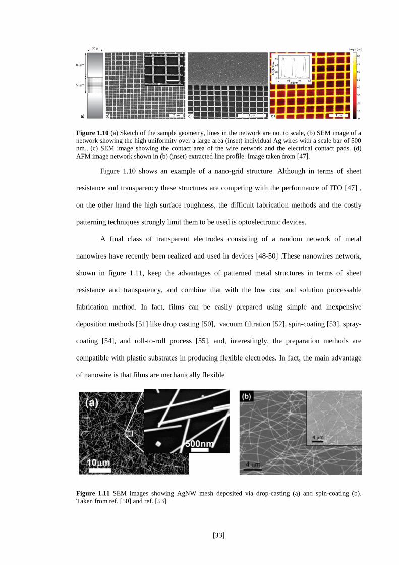
1.10 (a) Sketch of the sample geometry, lines in the network are not to scale, (b) SEM image of
a network showing the high uniformity over a large area (inset) individual Ag wires with a
scale bar of 500 nm., (c) SEM image showing the contact area of the wire network and the
electrical contact pads. (d) AFM image network shown in (b) (inset) extracted line profile.
Image taken from [47].
1.11 SEM images showing AgNW mesh deposited via drop-casting (a) and spin-coating (b).
Taken from ref. [50] and ref. [53].
1.12 A scanning electron micrograph of the micro-bull obtained by photopolymerisation, the
scale bar is 2 micrometres long. Taken from ref. [64].
1.13 (a) A scanning electron micrograph of an electrochemical micromachined microsystem
(MEMS) taken from ref. [70] and (b) a porous silicon microcavity taken from ref. [71].
1.14 (a) TEM cross-sectional image of an L-b-L assembled multilayer. Adapted from ref. [75]
(b) image of a polymer inverse opal, revealing the optimal replication process (inset)
detail of one hollow sphere, taken from ref. [83].

[7]
2.1 (a) sp3 hybridisation, where 4 σ bonds (in blue) are formed with an angle of 109.5° between
the bonding orbitals (b) sp2 hybridisation shows a trigonal-planar geometry with an angle
of 120° between the three σ bonds, the remaining π bonds (in green) are perpendicular to
the σ ones (c) in the sp hybridisation there are only two σ bonds with an angle of 180°
between them.
2.2 (a) Scheme of the sp2 hybridisation in an ethylene molecule (b) Scheme of the energy
splitting of 2p orbitals into a bonding and an antibonding orbital. Increasing the CH2 units
leads to an increase in the degeneration of energy levels resulting in two quasi-continuous
bands, namely the highest occupied molecular orbital (HOMO) and the lowest unoccupied
molecular orbital (LUMO).
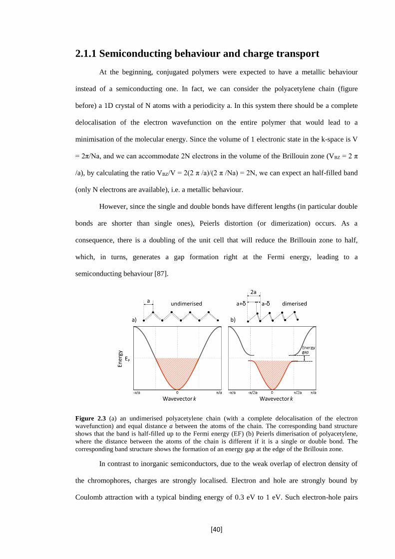
2.3 (a) An undimerised polyacetylene chain (with a complete delocalisation of the electron
wavefunction) and equal distance a between the atoms of the chain. The corresponding
band structure shows that the band is half-filled up to the Fermi energy (EF) (b) Peierls
dimerisation of polyacetylene, where the distance between the atoms of the chain is
different if it is a single or double bond. The corresponding band structure shows the
formation of an energy gap at the edge of the Brillouin zone.
2.4 Electronic energy level diagram of a solid showing the various energies relevant to the
definition of the work function.
2.5 Orientation of the dipoles induced by the adsorbate: (a) the adsorbate is polarised with the
positive pole towards the vacuum side causing a decrease in and (b) with the negative
pole pointing towards the vacuum side, causing am increase in.
2.6 Electric circuit of the Zisman’s KP set-up.
2.7 Jablonski diagram illustrating the different electronic and vibrational levels in an organic
molecule and, the different optical transitions.
2.8 Scheme of Morse potential energy curves with vibrational energy levels indicated for each
state. It illustrates the Franck-Condon principle and the origin of the symmetrical shape of
absorption and emission spectra in organic molecules. The difference between the maxima
of the absorption and fluorescence spectra is the Stokes’ shift.
2.9 Schematic illustration of H- and J-aggregates (exemplified for a dimer) for a π-conjugated
molecule (monomer). The ground state of the monomer is indicated as E0 and lowest
excited state as E1. Depending on the orientation of the interacting dipoles, E1 splits in
two different ways: (a) for a head-to-tail coupling (H-aggregate), the parallel orientation
will be at higher energy, while the energy of the antiparallel orientation will be lower than
the monomer level E1; (b) for cofacial coupling (J-aggregates), the dipole is coupled in
one dimension, with the same oriented at lower energy and the opposite oriented at higher
energy than the monomer level E1. Full arrows depict allowed (strong) transitions, and
dashed arrows forbidden (or weak) ones.
2.10 Electronics scheme for TCSPC, taken from [93].
2.11Three-dimensional schematic representation of perovskite structure ABX3 (A = CH3NH3,B
= Pb, and X = Cl, I, Br), taken from [97].
[8]
2.12 Equivalent electric circuit for a real solar cell.
2.13 J-V curve (in red) of a real device. The operating point with the maxima power is identified
by pair (Jmax; Vmax).
2.14 (a) Schematic mesostructured device architecture (on the left) and cross-sectional SEM
image of the device structure, taken from ref. [98].The transparent electrode is the
fluorinated-tin oxide (FTO), on top of it there is a compact layer of titania (TiO2) and the
mesoporous oxide. The perovskite is the photoactive layers, and it is infiltrated into the
mesoporous scaffold. Than the structure is capped with the hole transporter (in this case it
is the spiro-OMeTAD) and the cathode. (b) Cross-sectional SEM of a planar
heterojunction device. In particular this is the inverted architecture, with the transparent
cathode (ITO) in the bottom. Taken from ref. [104].
2.15 Schematic energy diagram of a solar cell in direct configuration, using FTO as transparent
electrode, TiO2 as ETL, Organo-Lead Perovskite ((CH3NH3)PbI3) as active layer, Spiro-
OMeOTAD as HTL and a generic metallic contact.
3.1 TEM/STEM images of rugate filter with reference peak (After infiltration) at 515 nm. (a)
Bright-field TEM image of the rugate filter (inset: photo of the same rugate filter). (b)
bright-field STEM overview image of the PhC (c) High Angle Annular Dark-Field zoom
of the internal structure (d) SEM image of a FIB-milled cross-section of the rugate filter at
515 nm detailing the pore structure, with pore sizes on the order of 50 nm or so. Bright
areas on the edge of the solid Si pillars are associated with regions of more intense
charging, and are thus assigned as rich in oxidised silicon, with a typical thickness of 10
nm or so.
3.2 2D-FFT transform (inset: frequency profile extracted from the 2D-FFT, the distance
between the lines is found to be 6.67 μm-1).
3.3 Bright-field TEM images taken at 12000 magnifications with 0.5 s exposure in the top and
bottom part of the rugate filter.
3.4 Reflectance spectra of the tuned (a) and detuned (b) rugate filter before (red line) and after
(blue line) the oxidation process.
3.5 (a) PL spectrum of a neat film of F8BT on a compact silicon substrate, and (b and c)
reflectance spectra for the PhCs before (blue) and after polymer infiltration (red). The
infiltration leads to a red-shift of the photonic stop-band (and thus of the reflectance peak)
of about 12±1 nm. Note that the vertical scales for (b) and (c) are different, i.e 40% and
100% reflectance, respectively. Inset: cartoon illustrating the inferred cross-section of the
rugate filter (D is the inter-planar spacing determined by the period of the anodic etching
current); the polymer layer is not filling the pores of the rugate filters, but there is just a
layer on the walls of the cavities (see main text for discussion). The structure of the
sample used to measure the F8BT PL is also shown.
3.6 (a) PL spectra (solid lines) collected at different incidence angle (from 0° to25° with step
of 5°) of the exciting beam for F8BT infiltrated into the tuned PhC and at 0° for the F8BT
infiltrated into the detuned PhC (dashed line). I used a CW laser, emitting at 405 nm, as
excitation source. I can observe the PL peak dispersion moving from 518 nm at 0° to 506

[9]
nm at 25°. (b) Ratio between the PL spectra from the tuned and detuned PhC at different
angles, as in (a) above.
3.7 Radiative decay of the F8BT PL measured by time-correlated single-photon counting,
TCSPC (371 nm excitation) and recorded either within the stop-band (528 nm, top panel)
and at the high-energy edge (518 nm, bottom panel) for a neat F8BT film on Si, as well as
for F8BT infiltrated into the tuned and detuned filters, as indicated in the plots legends.
4.1 SEM image of the opal structure (left) and photo of opals made with different microspheres
diameter (right), the diameter (in nm) is indicated below the opals. The reflected color
changes as function of the dimension, according to Bragg-Snell’s law.
4.2 Right: photonic band structure of an opal made with dielectric spheres (ε=13). The stop-
band is present along certain crystallographic directions (e.g. the Γ-L direction) but not for
every direction, thus it is not a complete photonic band-gap. Inset: FCC lattice structure;
taken from ref. [3]. Left: symmetry point in the Brillouin zone for a FCC lattice; taken
from ref. [137].
4.3 Photonic band structures and corresponding DOS and reflectance spectrum at normal
incidence. Adapted from ref. [137].
4.4 Density of states at different angles and for different orientations. Taken from ref. [137].
4.5 Chemical structures of the cyclodextrin-threaded conjugated polyrotaxanes with poly(4,4’-
diphenylene-vinylene) (PDV.Li) core with naphthalene stoppers (average number of
repeat units n = 10) and its optical properties (photoluminescence quantum efficiency,
PLQE, and OLES external quantum efficiency, EQE) as function of the threading ratio.
Reproduced from ref. [157].
4.6 (a) Scheme of the vertical deposition technique used to prepare the opals and (b) the
experimental set-up.
4.7 SEM micrographs of an opal film incorporating PDV.Li⊂β-CD: (a) cryo-cleaved wall
surface showing the internal structure of the opal, (b) film cross-section. Strong contrast
between the sphere and the interstices is observed, confirming that the latter are not filled
up by the conjugated polyelectrolytes (the density of the conjugated moiety and of the
spheres being comparable). Inset: Photography of the diffraction pattern from the opals.
Images were collected using the SEM mode of a dual beam Carl Zeiss XB1540 “Cross-
Beam” focussed-ion-beam microscope and the cross section was obtained via cryo-
cleaving an opal film. Adapted from ref. [110].
4.8 Reflectance spectra collected from opal made with microspheres with a diameter of (a) 200
nm, (b) 220 nm, (c) 370 nm and (d) 430 nm. Inset: scheme of the mapping.
4.9 Reflectance (blue line) and transmittance (red line) spectra of an opal prepared with
microspheres diameter = 220 nm.
4.10 Angle-resolved transmittance spectra for the opal made with microspheres diameter 430
nm for (a) p- and (b) s-polarised light.

[10]
4.11 Colored contour-plot of the transmittance spectra for the opal made with microspheres
diameter 430 nm for (a) p- and (b) s-polarised light. Transmittance percentage is shown in
color scale.
4.12 Transmittance spectra of the opals as a function of incidence angle for (a) 200 nm, (b) 220
nm and (c) 370 nm microspheres diameter. The Bragg-Snell law analysis of the spectra
appears in (d) where the lines are linear regressions. Taken from ref. [146].
4.13 Reflectance spectra of the bare opal made with microsphere diameter 200 nm (red) and
infiltrated (black) with the polyrotaxanes. There is no difference between the spectral
positions of the reflectance peaks.
4.14 Normalized reflectance spectra (coloured lines) of the bare opals and normalized PL
emission (black solid line) of polyrotaxanes inside a thermally annealed opal and of a
spin-coated thin film (black dashed line). The annealing was necessary to keep the
material chemical properties but avoiding the photonic contribution.
4.15 PL (black), reflectance (red) and transmittance (green) spectra collected at normal
incidence for spray-coated opals made with beads having diameter 200 nm (a) and 430 nm
(b).
4.16 (a) Angle resolved PL emission for infiltrated opals made with microspheres diameter 200
nm (a). The enhancement and suppression effects depend on the incident angle. This
effect can be better appreciated in (b) where I plot the PL ratio between the thin film and
the photonic structure at various angles.
5.1 (a) Scheme of the device prepared with the ordered nanostructure, (b) with the "standard"
titania mesoporous scaffold, and (c) with the perovskite coated on top of the compact
titania layer.
5.2 (a) Preparation steps for patterned titania photonic scaffolds: (1) PS microspheres
monolayer is obtained via self-assembling and transferred onto the FTO/c-TiO2, (2) drop-
casting of the oxide precursor solution onto the PS microsferes template. Complete filling
of the gaps of the monolayer is obtained leaving the samples drying overnight, (3) titania
microspheres replica structure forms after a three-steps annealing described in the
experimental section. AFM images (scalebars are 3 μm) show: (b) a typical highly-
ordered monolayer of PS microspheres with a diameter of 370 nm, and the calcinated
TiO2 monolayers obtained from PS microspheres with various diameter, in particualr: (c)
220 nm (inse in blue box: a zoomed images on the layer, the scale bar is 1 μm), (d) 270
nm and (e) 430 nm.
5.3 (a) Ar-milled XPS profile of the microspheres titania layer onto FTO/cTiO2 substrates.
Dr. Tiziana Fiore from University of Palermo for the measurement is thankfully
acknowledged for these measurements. (b) FIB-milled SEM micrograph (scalebar is 400
nm) of the titania hollow spheres monolayer.
5.4 XRD spectra of the titania nanostructures and the titania mesoporous layer sintered onto
FTO substrates and of the bare FTO. Anatase peaks of TiO2: 2 theta 25.37°, fluorine-
doped tin oxide (FTO) substrate peaks: 2 theta = 26.4°, 37.6°.These measurements were
taken by G. M. Paterno’ from our group.
[11]
5.5 Transmittance spectra of the titania structure synthesized onto the FTO substrates.
5.6 AFM (tapping mode) images of the perovskite layer synthesized onto the nanostructured
titania starting from (a) spheres having a diameter of 370 nm, (b) the mesoporous titania
layer and (c) on compact titania layer.
5.7 XRD spectra of the perovskite layer sintered onto FTO/cTiO2 (black line),
FTO/cTiO2/mesoporous (red line), and FTO/cTiO2/nanostructure (blue line for the
microspheres with 370 nm diameter, green line for the microspheres with 430 nm
diameter) substrates. Broader peaks (full width half maximum, FWHM, inset) for the
perovskite prepared onto the mesoporous and nanostructured films. These measurements
were taken by G. M. Paterno’ from our group.
5.8 Electrical characterization and device performance analysis: (a) J−V curves of the devices
both under illumination (darker curves) and in dark (lighter curves). The arrows highlight
the enhanced Jsc and Voc obtained for the cells prepared with the nanostructured titania
layer. (b-e) Box-plot of the devices performance: (b) power conversion efficiency (PCE),
(c) Fill Factor (FF), (d) open circuit voltage (Voc), and (e) short-circuit current density
(Jsc).
5.9 (a-d) One-diode model fitting (R2>0.97) for each titania scaffolds. (e) Series resistance (f)
and shunt resistance for devices obtained from the fitting of the current density – voltage
curve.
5.10 Hysteresis measurement of FTO/c-TiO2/370nm drop/Perovskite/Spiro-OmeTAD/Au.
6.1 (a) Spray-coating set-up and (b) schematic illustration of the components.
6.2 (a) Transmittance spectra (solid lines) for the various films deposited onto soda lime glass
slides compared to the transmittance of the bare glass slide (black dashed line) and ITO
onto glass (red dotted line). (b) Sheet resistance measured using a four points probe for the
various thin films.
6.3 (a-d) Atomic force microscopy topographies (tapping mode) of (a) AgNWs, (b) 5x
AgNWs-SWCNTs, (c) 7x AgNWs-SWCNTs, (d) SWCNTs thin films. Height scale has
been kept equal for each sample. (e) Roughness of the films (included for an ITO film),
that represents the standard deviation of surface heights calculated from AFM data and (f)
Peak-to-valley distances for the thin films.
6.4 (a) Transmittance spectra for the films deposited onto soda lime glass slides (blue and
light blue lines) and PET foils (red and light red lines) for the two thickness tested. (b)
Sheet resistance measured using a four points probe for films prepared onto soda lime
glass slide and PET foil. The value obtained for the film onto glass slide (for the thick
sample) is comparable to previous results, thus suggesting an optimal reproducibility of
the preparation method. Adapted from ref. [189].
6.5 AFM images of the CNTs networks with increasing densities, namely 12 CNT/μm2, 18
CNT/μm2 and 24 CNT/μm2. Adapted from ref. [32].

[12]
6.6 Measured (circles) and calculated (solid lines) relative resistance (defined as the ratio
between the initial resistance and the measured one at different temperature) of three
CNTs networks with different densities. The resistance decreases by increasing the
temperature for the denser networks. Instead, for the network with 12 CNTs/μm2 we
observe the presence of a minimum in the resistance. I thank Simone Colasanti for the
simulation. Taken from ref. [32].
6.7 Temperature dependency of the resistance for a network with 16 CNTs/μm2 measured and
simulated in air (red) and under nitrogen (blue). The different behavior of the network
could be attributed to a different oxygen desorption from the CNTs in the two
environments. I thank Simone Colasanti for the simulation. Taken from ref. [32].
6.8 WF measured (a) on the thin films before (black circle) and after different PEI deposition
and/or thermal treatments. (b) Difference between the WF after each treatment and the
pristine values. Inset: PEI chemical structure.

[13]
List of tables
3.1 Temporal decay constants (τ1, τ2) extracted from least square fits of the PL decay curves
with their relative weight (I1, I2).
4.1 Thickness of the opals made with different micorspheres diameters.

[14]
List of publications
1 Valentina Robbiano, Alaa Abdellah, Luca Santarelli, Aniello Falco, Sara El-Molla, Lyubov
V Titova, David N Purschke, Frank Hegmann, Franco Cacialli, Paolo Lugli, “Analysis of
sprayed Carbon nanotube films on rigid and flexible substrates”, Proceeding of
Nanotechnology (IEEE-NANO), 650-654, (2014).
2 Valentina Robbiano, Francesco Di Stasio, Salvatore Surdo, Shabbir Mian, Giuseppe
Barillaro, Franco Cacialli, “Hybrid-Organic Photonic Structures for Light Emission
Modification”, in Organic and Hybrid Photonic Crystals, Springer International
Publishing, 339-358 (2015).
3 Giovanni Polito, Salvatore Surdo, Valentina Robbiano, Giulia Tregnago, Franco Cacialli,
Giuseppe Barillaro, “Two‐Dimensional Array of Photoluminescent Light Sources by
Selective Integration of Conjugated Luminescent Polymers into Three‐Dimensional Silicon
Microstructures”, Advanced Optical Materials, 1: 894–898 (2013).
4 Francesco Di Stasio, Luca Berti, Shane O. McDonnell, Valentina Robbiano, Harry L
Anderson, Davide Comoretto, Franco Cacialli, “Fluorescent polystyrene photonic crystals
self-assembled with water-soluble conjugated polyrotaxanes”, APL Materials, 1, 042116
(2013).
5 Simone Colasanti, Valentina Robbiano, Florin C. Loghin, Ahmed Abdelhalim, Vijay D.
Bhatt, Alaa Abdellah, Franco Cacialli, Paolo Lugli, “Experimental and Computational Study
on the Temperature Behavior of CNT Networks”, IEEE Transactions on Nanotechnology,
15 (2016) 171-178.
6 Simone Colasanti, Florin C. Loghin, Ahmed Abdelhalim, Vijay D. Bhatt, Alaa Abdellah.,
Paolo Lugli, Valentina Robbiano, Franco Cacialli "Experimental and computational study
on the temperature behavior of CNT networks", Proceeding of Nanotechnology (IEEE-
NANO), 1445-1448. (2015).
7 Gina Mayonado, Shabbir Mian, Valentina Robbiano, Franco Cacialli, “Investigation of the
Bragg-Snell law In photonic crystals”, Proceeding of BFY Conference, 60-63, (2015).
8 Giuseppe Barillaro, Giovanni Polito, Salvatore Surdo, Valentina Robbiano, Giulia
Tregnago, Franco Cacialli, “Synergic Integration of Conjugated Luminescent Polymers and
Three-Dimensional Silicon Microstructures for the Effective Synthesis of Photoluminescent
Light Source Arrays”, in Sensors, Springer International Publishing, 319: 243-247
(2015).
9 Luca Nucara, Vincenzo Piazza, Francesco Greco,Valentina Robbiano, Valentina Cappello,
Mauro Gemmi, Franco Cacialli, Virgilio Mattoli, “Ionic Strength Responsive Sulfonated
Polystyrene Opals”, accepted to ACS Applied Material & Interfaces.
10 Giuseppe M. Paternò, Valentina Robbiano, Keith J. Fraser, Christopher Frost, Victoria
García Sakai, Franco Cacialli, “Neutron Radiation Tolerance of Two Benchmark Thiophene-
Based Conjugated Polymers: the Importance of Crystallinity for Organic Avionics”,
accepted to Scientific Reports.

[15]
11 Valentina Robbiano, Salvatore Surdo, Giancarlo Canazza, G. Mattia Lazzerini, Shabbir
Mian, Davide Comoretto, Giuseppe Barillaro, Franco Cacialli, “C-Si hybrid photonic
structures by infiltration of conjugated polymers into porous silicon rugate filters”, in
preparation.
12 Valentina Robbiano, Giuseppe M. Paternò, Giovanni F. Cotella, Tiziana Fiore, Martina
Dianetti, Francesca Brunetti, Bruno Pignataro, Henry J. Snaith, F. Cacialli, “Nanostructured
titania for efficient perovskite solar cells”, in preparation.

[16]
Introduction
In the last 30 years, there has been an increasing interest in the development of novel
micro- and nano-structure to control the interaction between light and matter, as well as to
exploit novel optical and electrical properties. The aim of this thesis is the investigation of
functional nanostructures for optoelectronic devices. One important class of nano-structure are
the photonic crystals.
The concept of a photonic crystal (PhC) was introduced in 1987 with the independent
studies of Yablonovitch [1] and John [2] on the inhibition of the spontaneous emission and light
localization effects. These relate to structures whose periodicity in refractive index would
enable to control, suppress, or enhance the propagation of photons, in analogy with the already
well-established possibility to control electron propagation in “electronic” crystals, in which the
periodicity of the electronic potential results in allowed and forbidden energy bands for the
electrons. As well-described by Joannopolous and collaborators in their book [3], this is due to
the possibility to re-write Maxwell equations in terms of a single master equation, in which the
dielectric function plays a similar role to the potential in Schrödinger's equation.
The spectral position of the photonic gap can thus be modulated by varying two
parameters: the materials of the components of refractive index and the pitch of the dielectric
pattern. The materials used to create this type of structures can be both inorganic and organic. In
the past years, the potential of these technologies has been considered with increasing attention
from academia, industry and institutions that aim to develop a new technology based on
photonic nanostructures for the exchange and processing of optical signals instead of electrical.
Indeed, the field of nano-structures and photonic crystals has then developed in a
variety of directions, often dictated by the hurdles of fabrication of structures whose periodicity
needs to be on the same lengthscale as that of the wavelength of the light one desires to control.
In fact, they exhibit a variety of properties that can be exploited in a many optoelectronics
applications, such as optical fibres [4], sensors [5], solar cells [6], light-emitting diodes [7] and
lasers [8].

[17]
Conjugated semiconducting polymers have been widely used as active materials in all
these applications. This is mainly due to their versatile processing, wide colour tuneability (from
near-infrared (NIR) to near ultraviolet (UV)), high solid-state photoluminescence efficiency and
strong optical absorption (up to ~105 cm-1) [9, 10]. Since the discovery of their electrical
conductivity in 1977 [11], they have attracted increasing attention due to interesting
optoelectronics properties and processing advantages for the realization of optoelectronic
devices such as light-emitting diodes [12], and photovoltaic devices [13].
The fundamental optical and electrical properties of organic semiconductors do not
derive from the crystal structures, as for inorganic semiconductors, but they arise from the
energy levels of the molecules that form the polymers chain and their intermolecular
interactions. This fundamental difference is the main advantage of the organic systems
compared to inorganic ones, for novel applications in the field of optoelectronics. In fact, the
optoelectronic properties of the organic semiconductors can be simply tailored by molecular
design, obtaining the desired electrical and optical properties.
More recently, organo-halide perovskite, have attracted great interest by obtaining in a
short time span significant increase in the power conversion efficiency (PCE) of photovoltaics
devices [14]. In fact, this metallo-organic system has demonstrated huge potential, joining the
good optoelectronic properties of metals to the ease of fabrication typical of organic materials
[15].
Thesis overview
The aim of the project is to prepare and characterise novel nano- and micro-structured
architectures using different techniques and to assess their potential for being implemented into
optoelectronic devices and components. As will be shown in the following chapters, these
structures show optical and electrical properties which are significantly different from bulk
materials, giving a new insight on how the nanoscale ordering affects their physical properties.
This thesis is divided into six chapters. The first two chapters give a general
introduction on nano- and micro-structures and organic-hybrid semiconductors, the

[18]
experimental techniques used and their applications in optoelectronic devices. The description
and discussion of experimental results are presented in the four following chapters. Brief
descriptions of the content of these chapters are given as follows:
In Chapter 3, I present an example of hybrid one-dimension photonic crystal,
specifically silicon rugate filters infiltrated with a luminescent polymer. I characterise their
internal structure and their optical properties.
In Chapter 4, the optical properties of synthetic opals, a particular class of three-
dimension photonic crystals, are shown. Such structures enable emission modification of a
supramolecular engineered conjugated polymer self-assembled inside them.
In Chapter 5 I present how it is possible to improve the efficiency of organo-halide
perovskite solar-cells using colloidal lithography to enhance light-trapping and boost perovskite
crystallization.
In Chapter 6, I show the morphological, electrical and optical characteristics of carbon
nanotubes and silver nanowires thin films obtained using spray-coating deposition, which can
be exploited as transparent conductive electrodes. Furthermore, I show how it is possible to tune
their work function to lower the injection barrier at electrode/active layer interfaces in
optoelectronic devices.
Finally, a summary of the results obtained as well as an outlook on future work is given.
[19]
Chapter 1
Nano- and Micro-structures
In this chapter I will present two categories of nano- and microstructures suitable for
light and charge managing: photonic crystals (PhCs) and nanostructured conductive thin films.
In the first part, the focus is given to photonic crystals and their optical properties. PhCs are
functional materials that can provide a variety of optical effects ranging from optical switching
to the modification of the emission spectra of active materials. In the second part I will discuss
the fundamental properties of nanostructured material suitable for transparent conductive
electrodes. These structures, widely applied in optoelectronic and electrochemical devices, need
to combine high electrical conductivity and high optical transparency in the visible spectrum.
1.1 Photonic Crystals
1.1.1 Photonic band formation
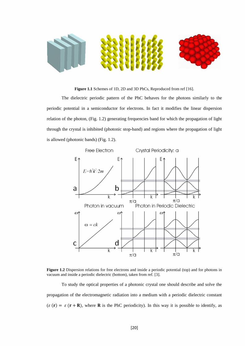
Photonic crystals are composite materials made by media with different dielectric
function (ε) or refractive index (n), periodically ordered in 1, 2 or 3 dimension (Fig. 1.1). The
path width of such structures is comparable to UV-Vis-NIR wavelengths[3]. The definition of
photonic crystal was introduced in 1987, with the pioneering and independent studies of
Yablonovitch [1] and John [2] on the inhibition of the spontaneous emission and on the
localization of the light. This stimulated early research on synthetic photonic crystals.
[20]
Figure 1.1 Schemes of 1D, 2D and 3D PhCs, Reproduced from ref [16].
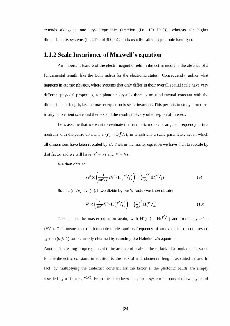
The dielectric periodic pattern of the PhC behaves for the photons similarly to the
periodic potential in a semiconductor for electrons. In fact it modifies the linear dispersion
relation of the photon, (Fig. 1.2) generating frequencies band for which the propagation of light
through the crystal is inhibited (photonic stop-band) and regions where the propagation of light
is allowed (photonic bands) (Fig. 1.2).
Figure 1.2 Dispersion relations for free electrons and inside a periodic potential (top) and for photons in
vacuum and inside a periodic dielectric (bottom), taken from ref. [3].
To study the optical properties of a photonic crystal one should describe and solve the
propagation of the electromagnetic radiation into a medium with a periodic dielectric constant
(𝜀 (𝐫) = 𝜀 (𝐫 + 𝐑), where 𝐑 is the PhC periodicity). In this way it is possible to identify, as

[21]
function of the dielectric parameters and geometry of the crystal itself, the permitted and
prohibited modes.
This problem can be solved by means of Maxwell’s equations:
∇ ∙ 𝐁 = 0 ∇ ×𝐄 + 1
𝑐 𝜕𝐁
𝜕𝑡= 0 (1)
∇ ∙ 𝐃 = 4πρ ∇ ×𝐇 − 1
𝑐 𝜕𝐃
𝜕𝑡=
4π
𝑐𝐉
As we are dealing with dielectric materials, Maxwell’s equations can be simplified by
making the following assumptions:
There are no currents or free charges and the media are not magnetic (ρ=0, J=0,
and μ=0, so B=H);
We approximate the electric field in the linear regime: 𝐃(𝐫) = ε(𝐫)𝐄(𝐫));
The material is macroscopic and isotropic, so 𝜀(𝐫, 𝜔) is a scalar dielectric
function;
Any explicit frequency dependence could be ignored 𝜀(𝐫, 𝜔) = 𝜀(𝐫);
𝜀(𝐫) could be considered purely real and positive, ignoring any absorption
effects.
Considering the linearity of Maxwell’s equation, it is possible to separate the time and
spatial dependence of E and H by expanding them in a set of harmonic modes at angular
frequency (𝜔).
In this way one obtains:
∇ ∙ 𝐇(𝐫) = 0 and ∇ ∙ 𝐃(𝐫) = 0 (2)
∇ × (1
𝜀(𝐫)∇×𝐇(𝐫)) = (
𝜔
𝑐)
2𝐇(𝐫) (3)
The first equations (2) indicate that the electromagnetic waves are transverse, i.e. the
field oscillates in a plane orthogonal to the propagation direction. That means, if we have a
plane wave 𝐇(𝐫) = 𝒂𝑒(𝑖𝒌 ∙𝐫) , with 𝒌 wave-vector, Eq. 2 requires that 𝒂 ∙ 𝒌 = 0. On the other

[22]
hand, equation 3 (known as Helmholtz’s equation or master equation) describes the propagation
of electromagnetic radiation in a medium with dielectric constant 𝜀(𝐫). Together, these two
equations enable the determination of 𝐇(𝐫). Furthermore, by defying the operator 𝚯 as:
𝚯𝐇(𝐫) = ∇ × (𝟏
𝜀(𝐫)∇×𝐇(𝐫)) (4)
the Helmholtz’s equation, which describes the propagation of light in a photonic crystal,
is reduced to an eigenvalue problem:
𝚯𝐇(𝐫) = (𝜔
𝑐)
2𝐇(𝐫) (5)
A photonic crystal has continuous translational symmetry in the directions in which the
medium is homogeneous and a discrete translational symmetry in the directions in which the
medium is periodic. In general, a system that has continuous translational symmetry is such that
it remains unchanged when shifted by a distance d. 𝐓𝐝 is defined as translation operator which,
acting on a generic function 𝒇(𝐫), shifts the argument by d. In a photonic crystal, we have:
𝐓𝐝𝜀(𝐫) = 𝜀(𝐫 + 𝐝) = 𝜀(𝐫). Since 𝐓𝐝 is defined as a symmetry operator of the system, one could
then apply 𝐓𝐝 to an eigenstate 𝐇 of 𝚯. A mode with the functional form 𝑒𝒊𝒌𝒛 is an eigenfuntion
in a system with continuous translational symmetry along a z-direction:
𝐓𝐝𝑒𝑖𝒌𝑧 = 𝑒𝑖𝒌(𝑧+𝐝) = 𝑒𝑖𝒌𝐝𝑒𝑖𝒌𝑧 (6)
Plane waves are eigenfunctions of 𝐓𝐝 and 𝑒𝑖𝒌𝑧 are the eigenvalues. It is then possible to
classify the modes by using the wave vector 𝒌. Therefore, in a homogeneous medium the modes
must have the form:
𝐇𝒌(𝐫) = 𝐇𝟎𝑒𝒊𝒌∙𝑟 (7)
Where 𝐇𝟎 is any constant vector. These plane waves are solutions of the Helmholtz
equation with eigenvalues (𝜔
𝑐)
2= 𝒌2 and imposing he transversality requirement , 𝒌 ∙ 𝐇𝟎 = 0.
In a PhC the discrete translational symmetry means that the system is periodic and the
basic step length is an integer that is be equal to the lattice constant of the crystal itself, defined
as R.

[23]
When 𝜀 (𝐫) = 𝜀 (𝐫 + 𝐑), the solutions, eigenstates of both operators 𝐓𝐝 and 𝚯, should
be plane waves modulated by a periodic function :
𝐇𝒌 = 𝑒𝒊𝒌∙𝑟𝒖𝒌(𝐫) (8)
where 𝒖𝒌(𝐫) is a periodic function on the lattice: 𝒖𝒌(𝐫) = 𝒖𝒌(𝐫 + 𝐑).
This result is known as the Bloch - Floquet theorem and is analogous to the Bloch
theorem on the electronic eigenstates in a crystal. Because of the periodic boundary condition,
the wavevector which identifies the modes can be selected within the range
− 𝜋 𝑎 < 𝒌 < + 𝜋 𝑎⁄⁄ (Brillouin zone), which contains non-redundant values of 𝒌. For each 𝒌
the Helmoltz equation admits as solutions 𝜔 = 𝜔𝑛(𝒌), where 𝑛, the band index that increases
with the frequency of the mode.
The consequence of that discrete translational symmetry is that the resolution of the
fundamental equation for the propagation of the electromagnetic radiation in a periodic medium
leads to modes having 𝒌𝑧 = 𝒎 2𝜋 𝑎⁄ , with m integer, and therefore have the same eigenvalues
(i.e.they are degenerate modes).
Figure 1.3 Scheme of the dispersion relation of a homogeneous medium (dashed line) and a 1D photonic
crystal (solid line). Reproduced from ref. [3].
For a homogeneous material the dispersion curve is continuous (Fig. 1.3). For a crystal,
indeed, the curve has a similar trend for small 𝒌, but it presents a maximum and a minimum at
the point 𝒌 = 1/2 (in (2π/a units). Radiation with frequency values within the forbidden band
cannot propagate inside the crystal. Such a region can be defined as photonic stop-band when it
[24]
extends alongside one crystallographic direction (i.e. 1D PhCs), whereas for higher
dimensionality systems (i.e. 2D and 3D PhCs) it is usually called as photonic band-gap.
1.1.2 Scale Invariance of Maxwell’s equation
An important feature of the electromagnetic field in dielectric media is the absence of a
fundamental length, like the Bohr radius for the electronic states. Consequently, unlike what
happens in atomic physics, where systems that only differ in their overall spatial scale have very
different physical properties, for photonic crystals there is no fundamental constant with the
dimensions of length, i.e. the master equation is scale invariant. This permits to study structures
in any convenient scale and then extend the results in every other region of interest.
Let's assume that we want to evaluate the harmonic modes of angular frequency 𝜔 in a
medium with dielectric constant 𝜀′(𝐫) = 𝜀(𝐫s⁄ ), in which s is a scale parameter, i.e. in which
all dimensions have been rescaled by 's'. Then in the master equation we have then to rescale by
that factor and we will have 𝒓′ = 𝒓s and ∇′= ∇s .
We then obtain:
s∇′ × (1
𝜀(𝐫′/𝑠)s∇′×𝐇 (𝐫′
s⁄ )) = (𝜔
𝑐𝑠)
2𝐇(𝐫′
s⁄ ) (9)
But is 𝜀(𝐫′/𝒔) is 𝜀′(𝐫). If we divide by the ’s’ factor we then obtain:
∇′ × (1
𝜀(r′)∇′×𝐇 (𝐫′
s⁄ )) = (𝜔
𝑐)
2𝐇(𝐫′
s⁄ ) (10)
This is just the master equation again, with 𝐇′(𝐫′) = 𝐇(𝐫′s⁄ ) and frequency 𝜔′ =
(𝜔s⁄ ). This means that the harmonic modes and its frequency of an expanded or compressed
system (s ≶ 1) can be simply obtained by rescaling the Helmholtz’s equation.
Another interesting property linked to invariance of scale is the to lack of a fundamental value
for the dielectric constant, in addition to the lack of a fundamental length, as stated before. In
fact, by multiplying the dielectric constant for the factor s, the photonic bands are simply
rescaled by a factor 𝑠−1/2. From this it follows that, for a system composed of two types of
[25]
materials with dielectric constants 𝜀1 and 𝜀2, the photonic band structure depends only on the
dielectric contrast 𝛥𝜀.
1.1.3 Bragg-Snell’s Law
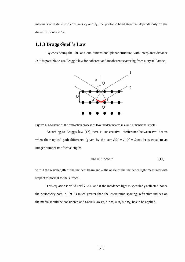
By considering the PhC as a one-dimensional planar structure, with interplanar distance
D, it is possible to use Bragg’s law for coherent and incoherent scattering from a crystal lattice.
Figure 1. 4 Scheme of the diffraction process of two incident beams in a one-dimensional crystal.
According to Bragg's law [17] there is constructive interference between two beams
when their optical path difference (given by the sum 𝐴𝑂′ = 𝐴′𝑂′ = 𝐷 cos 𝜃) is equal to an
integer number 𝑚 of wavelengths:
𝑚𝜆 = 2𝐷 cos 𝜃 (11)
with 𝜆 the wavelength of the incident beam and 𝜃 the angle of the incidence light measured with
respect to normal to the surface.
This equation is valid until λ < D and if the incidence light is specularly reflected. Since
the periodicity path in PhC is much greater than the interatomic spacing, refractive indices on
the media should be considered and Snell’s law (𝑛𝑖 sin 𝜃𝑖 = 𝑛𝑡 sin 𝜃𝑡) has to be applied.

[26]
Figure 1. 5 Scheme of the diffraction model of one-dimensional photonic crystal.
Where 𝜃𝑖and 𝜃𝑡are the incidence and refraction angles and 𝑛𝑖 and 𝑛𝑡 are the refractive
indices of the two media. By setting air as one of the medium ( 𝑛𝑖 = 1) we obtain
sin 𝜃𝑖 = 𝑛𝑒𝑓𝑓 sin 𝜃𝑡 (12)
where 𝑛𝑒𝑓𝑓 is the effective refractive index of the PhC. This is calculated by using the Lorentz-
Lorenz equation, where the refractive indices of the media are weighted by their volume
fraction 𝑓𝑛:
𝑛𝑒𝑓𝑓2 −1
𝑛𝑒𝑓𝑓2 +2
= ∑ 𝑓𝑛𝑛𝑛
2 −1
𝑛𝑛2 +2𝑛 (13)
The optical path is equal to the geometric path multiplied by the effective refractive
index:
𝑚𝜆 = 2(𝑛𝑒𝑓𝑓𝐵𝑂′ − 𝐸𝑂) (14)
with
𝐵𝑂′ =𝐷
cos 𝜃𝑡=
𝐷𝑛𝑒𝑓𝑓
√𝑛𝑒𝑓𝑓2 −sin2𝜃
(15)
and
𝐸𝑂 = 𝐵𝑂 sin 𝜃 =𝐷sin2𝜃
√𝑛𝑒𝑓𝑓2 −sin2𝜃
(16)

[27]
as obtained by straightforward geometrical considerations.
The Bragg-Snell’s law is then obtained from Eq. 12 by substituting 𝐵𝑂′ and 𝐸𝑂 with
the solutions of the equations above (13 and 14):
𝑚𝜆 = 2(𝑛𝑒𝑓𝑓𝐵𝑂′ − 𝐸𝑂) = 2 (𝐷𝑛𝑒𝑓𝑓
2
√𝑛𝑒𝑓𝑓2 −sin2𝜃
−𝐷sin2𝜃
√𝑛𝑒𝑓𝑓2 −sin2𝜃
) = 2𝐷√𝑛𝑒𝑓𝑓2 − sin2𝜃 (17)
Where 𝜆 is the spectral position of the photonic stop-band that depends on the angle of
the incident light θ, the interplanar spacing between the media D and the refractive indices and
volume fraction of the media (contained in neff2 ).
1.1.4 Density of states
The density of state (DOS) of a system is the number of allowed state per unit interval
of frequency ω[18]. The optical properties of an emitter strongly depend of the DOS, according
to the Fermi’s golden rule. The density of states of the radiation field in the volume V of free
space, D(ω), is proportional to ω2:
𝐷(𝜔) =𝜔2𝑉
𝜋2𝑐3 (18)
The density of states in the uniform material is obtained by replacing c by v = c/n in this
equation. In a PhC, within the photonic-gap no modes are allowed, and therefore the density of
states (defined as the number of possible modes per unit frequency) is zero.
The optical properties of atoms and molecules strongly depend on D(ω). A way to
control and modify D(ω), and in turn the emission properties and radiative rate of emitters, is to
use photonic crystals.

[28]
Figure 1.6 Schematic illustration of the density of states of the radiation field in free space (dashed blue
line) and (a) in a photonic crystal featuring a stop-band (red line) and (b) in a photonic crystal featuring a
full band-gap (green line).
In particular, when an active material is embedded into a PhC, its optical properties are
strongly affected by the periodical dielectric environment, which alter the dispersion properties
of photons (i.e. photonic density of states, p-DOS)[19]. Indeed, the p-DOS diminishes within
the photonic band gap thus suppressing light-emission. On the other hand, at the edges of the
photonic band gap, the p-DOS increases [20], i.e. a light-emission enhancement is observed.
Both enhancement and suppression of the emitted light are accompanied by an increase and
decrease of the radiative rate, respectively. Such an effect on the radiative rate can be used to
modify, for example, the photoluminescence spectrum of the embedded material. In fact, as
discussed in Chapter 2, the photoluminescence quantum yield is function of the emission
lifetime (τ), which depends on the DOS via the Fermi’s golden rule [21]:
𝑅𝑖→𝑓
(𝜔) =2𝜋
ℏ|⟨𝑓|𝐻′|𝑖⟩|2𝜌(𝜔) (19)
where R is the transition probability from an initial state i to a finale state f and is
related to the mean lifetime τ (R = 1/τ), ρ is the density of final states and |⟨𝑓|𝐻′|𝑖⟩|2 is the
matrix element of the perturbation H' between the final and initial states. This matrix element
depends on the coupling between the initial and final stated of the system.
[29]
1.2 Transparent and conductive nanostructured
thin films
Nowadays, great efforts have been made to replace indium tin oxide (ITO). So far ITO
has been commonly used in many applications but it has some drawbacks, such as the high cost,
the scarcity of indium and the brittleness[22] that limit its application mainly in flexible
devices. Innovative nanostructured materials, such as carbon nanotubes (CNTs) and metal
nanowires have been demonstrated to be good candidate to replace ITO as transparent
conductive electrodes (TCE) in optoelectronic devices. In this regard, the two most important
parameters are the TCE sheet resistance and optical transparency[23]. In particular, an
optimized electrode typically transmits >80% in the visible spectral range and its sheet
resistances (Rsheet) should be less than 20 Ω/ [24].
1.2.1 CNTs
CNTs were first synthesized in 1991 by Iijima and Ichihashi [25, 26] at NEC
laboratories in Japan. Since their discovery, CNTs have been extensively studied thanks to their
outstanding electrical and mechanical properties. In fact, their unique characteristics, in addition
to their nanoscale size, enabled them to be used in a variety of applications.
Carbon nanotubes can be thought of as a rolled-up sheet of graphite, closed at each end.
They can be multi-walled or single-walled. A single-walled carbon nanotube (SWCNT) consists
of just one layer of graphite and it has a diameter around 1nm, while a multi-walled nanotube
(MWCNT) has multiple concentric layers and it can have an outer diameter ranging from 2.5nm
to 30nm [27] (Fig. 1.7).

[30]
.
Figure 1.7 Schematic illustration of a SWCNT (a) and (b) of a MWCNT, with their typical dimensions.
Taken from ref. [28].
Carbon nanotubes can be either conducting or semi-conducting along their tubular axis
[29-31]. Some nanotubes appear to exhibit ballistic conduction along the tube, which is a
characteristic of a quantum wire [27, 32]. Ballistic conduction or transport is when electrons are
able to flow without colliding into impurities or being scattered by phonons.
Despite such fascinating properties, significant challenges emerged for CNTs films. In
fact, transport mechanisms are still not completely clear, especially at the junction between two
tubes. In addition, considering that commercially available CNTs are often a mixture of
nanotubes with different electrical properties, the study of these films is a non-trivial task.
Typically, these junctions between nanotubes have high resistance in the range of 200 kΩ - 20
MΩ [33]; hence, the conductivity of CNT films is reduced drastically compared to that of a
single CNT that have a carrier mobility of ~10,000 cm2V−1s−1 [34]. Some approaches have been
introduced to reduce the sheet resistance of the CNT films such as treating CNTs with acid and
using longer CNTs [35]. The semiconductor nanotubes have much lower conductivity than the
metallic tubes [33] and so do not contribute much to the conductivity. Furthermore, they absorb
light and so reduce transparency. In addition, metal/semiconductor junctions in CNT films
create high contact resistance due to Schottky barrier formation, resulting in higher sheet
resistance [33]. Separating metal and semiconductor CNTs or producing metallic only CNT are

[31]
still serious challenges [36]. Although some methods have been introduced to separate metal
nanotubes, most of them are not yet suitable for large-scale technological processes.
Figure 1.8 (a) Sketch of an electrophoretic cell and photos of SWCNTs solution in before and 4, 16, and
24 h after the application of 30V (taken from ref. [37]) and (b) Separation of semiconducting SWCTs
starting from a mixed metallic semiconducting solution obtained via ultracentrifugation method. The
separation can be observed both in the photo and in the absorbance spectra. Adapted from ref. [38].
The most efficient methods, with examples reported in Fig. 1.8, rely on density-
gradient ultracentrifugation [38-40], which separates nanotubes dispersed in a solution with a
surfactant exploiting the difference in their density, and vertical electrophoresis, where an
aqueous solution of mixed SWCNTs is separated into metallic and semiconducting nanotubes
simply applying an electric field along the cell [37, 41, 42].
1.2.2 Metal nanostructures
Metal nanostructures are an appealing alternative to ITO and many other transparent
electrodes since metals have the highest conductivity of all types of materials. On the other
hand, the major drawback of metallic materials is the very low transparency of metals to visible
light. The only possible way to fabricate transparent electrodes using metallic structures is to
use nanostructured materials. Metal nano-grids, ultra-thin metal films (of less than 10 nm
thickness) and random networks of metal nanowires are three of the most used structures to
make transparent electrodes [35].
Metal films can be used as transparent electrodes when they are sufficiently thin,
usually less than few tens on nm, at which point they become transparent to visible light [43-
45]. In fact, the biggest trade-off in using these materials is that films need to be thin enough to
transmit sufficient light without becoming discontinuous and start to suffer from poor electrical

[32]
conductivity. The main issue is that for metal such Ag and Au, the conductivity would be good
at thicknesses for which the transmission remains high. This is due to the intrinsic instability of
ultra-thin films, where there is a tendency to coalescence of mostly un-connected grains, which
generally prevents their application as transparent electrodes.
Figure 1.9 Average optical transmittance in the visible range as function of the t electrical resistivity for
Cr and Ni films compared with ITO anneal and not annealed. Reproduced from ref. [45].
Figure 1.9 illustrates the sheet resistances and transparencies of Cr and Ni thin films of
various thicknesses [45]. In addition to the low transparency and conductivity values, metallic
thin film deposition happens at ultrahigh vacuum by DC sputtering, which has a high
manufacturing cost [35].
Metal nano-grids consist of ordered metal strip lines and are normally patterned by
complex fabrication processes such as nanoimprint lithography [46] and electron beam
lithography [35, 47]. The main advantage of these structures compared to thin films is that the
total transmission is dramatically increased. In fact, whereas through the metal strips the
transmittance is almost zero, in the gaps between them the transmittance is 100%. Therefore, the
total transmittance, defined by the percentage of the total area that is covered by the metal grid,
can reach values similar to the one of ITO [47]. However, this increase in transparency comes at
the price of an increased surface roughness.
[33]
Figure 1.10 (a) Sketch of the sample geometry, lines in the network are not to scale, (b) SEM image of a
network showing the high uniformity over a large area (inset) individual Ag wires with a scale bar of 500
nm., (c) SEM image showing the contact area of the wire network and the electrical contact pads. (d)
AFM image network shown in (b) (inset) extracted line profile. Image taken from [47].
Figure 1.10 shows an example of a nano-grid structure. Although in terms of sheet
resistance and transparency these structures are competing with the performance of ITO [47] ,
on the other hand the high surface roughness, the difficult fabrication methods and the costly
patterning techniques strongly limit them to be used is optoelectronic devices.
A final class of transparent electrodes consisting of a random network of metal
nanowires have recently been realized and used in devices [48-50] .These nanowires network,
shown in figure 1.11, keep the advantages of patterned metal structures in terms of sheet
resistance and transparency, and combine that with the low cost and solution processable
fabrication method. In fact, films can be easily prepared using simple and inexpensive
deposition methods [51] like drop casting [50], vacuum filtration [52], spin-coating [53], spray-
coating [54], and roll-to-roll process [55], and, interestingly, the preparation methods are
compatible with plastic substrates in producing flexible electrodes. In fact, the main advantage
of nanowire is that films are mechanically flexible
Figure 1.11 SEM images showing AgNW mesh deposited via drop-casting (a) and spin-coating (b).
Taken from ref. [50] and ref. [53].

[34]
Among the various metal that can be exploited in the preparation of nanowires (Ag, Cu
and Au) [51], silver is one of the most promising since it does not tend to oxidise, it has high
DC conductivity and a relatively low cost compared with other alternatives. So far, silver
nanowire electrodes show superior performance compared to graphene and CNTs [48].
Copper nanowires are also being used for transparent conductors since copper is
cheaper than silver and has high conductivity. Reported copper (and copper-based) nanowire
transparent electrodes show superior performance than CNTs and comparable to silver
nanowires and ITO [51].The main concern of using copper nanowires is their instability in air
due to the fact that copper reacts with atmospheric oxygen and thus need to be passivated to
prevent oxidation when used as electrodes. [56, 57].
1.3 Nano- micro-structuring techniques
The field of nanostructures and photonic crystals has developed in a variety of
directions, often dictated by the hurdles of fabrication of structures whose periodicity needs to
be on the same lengthscale as that of the wavelength of the light one desires to control or the
desired surface roughness [58]. This places some stringent requirements, as one needs to
generate patterns with typical dimensions/periodicities of the order of a few hundreds of
nanometres. Typical fabrication methods can be dived into two major classes: top-down and
bottom-up approaches.
1.3.1 Top-Down approaches
So far, the development and production of nanostructures has been generally focused on
top-down nanofabrication[59-62] making use of lithographic techniques such as electron-beam
and focused ion-beam patterning (FIB). These are very expensive, and being essentially “serial”
suffer from significant limitations in terms of either surface areas or sample throughput, in
addition to being limited to the fabrication of mainly two-dimensional structures. Another major
drawback is that the photonic effects are strongly inhibited by the residual surface roughness,
thus spoiling the overall Q-factor of the cavities[63]. One technique that has shown more
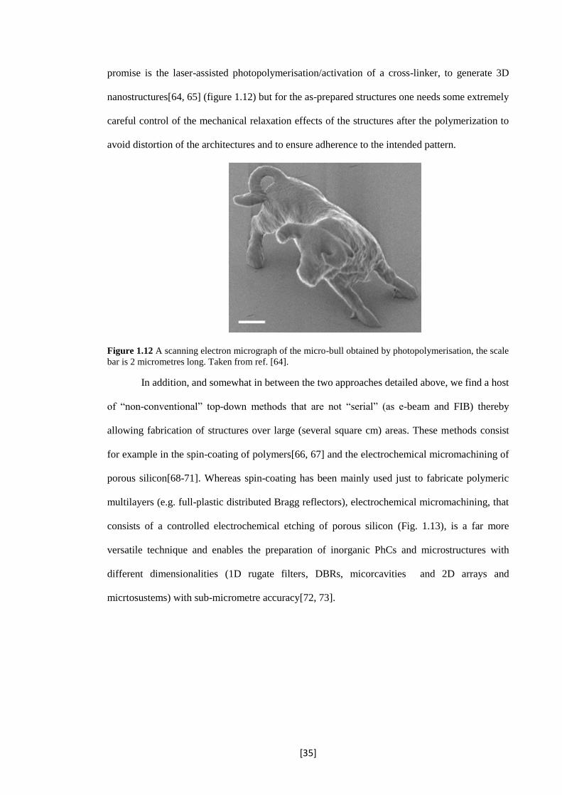
[35]
promise is the laser-assisted photopolymerisation/activation of a cross-linker, to generate 3D
nanostructures[64, 65] (figure 1.12) but for the as-prepared structures one needs some extremely
careful control of the mechanical relaxation effects of the structures after the polymerization to
avoid distortion of the architectures and to ensure adherence to the intended pattern.
Figure 1.12 A scanning electron micrograph of the micro-bull obtained by photopolymerisation, the scale
bar is 2 micrometres long. Taken from ref. [64].
In addition, and somewhat in between the two approaches detailed above, we find a host
of “non-conventional” top-down methods that are not “serial” (as e-beam and FIB) thereby
allowing fabrication of structures over large (several square cm) areas. These methods consist
for example in the spin-coating of polymers[66, 67] and the electrochemical micromachining of
porous silicon[68-71]. Whereas spin-coating has been mainly used just to fabricate polymeric
multilayers (e.g. full-plastic distributed Bragg reflectors), electrochemical micromachining, that
consists of a controlled electrochemical etching of porous silicon (Fig. 1.13), is a far more
versatile technique and enables the preparation of inorganic PhCs and microstructures with
different dimensionalities (1D rugate filters, DBRs, micorcavities and 2D arrays and
micrtosustems) with sub-micrometre accuracy[72, 73].

[36]
Figure 1.13 (a) A scanning electron micrograph of an electrochemical micromachined microsystem
(MEMS) taken from ref. [70] and (b) a porous silicon microcavity taken from ref. [71].
1.3.2 Bottom-up approaches
By contrast, bottom-up approaches exploit the collective self-assembly of suitably-sized
building blocks (typically colloidal dielectric microspheres or charged polyelectrolytes). This
provides a much easier, faster, and low cost alternative to top-down methods in preparing
photonic crystals and nanostructures, enabling the preparation nanostructured multilayers
exploiting the so-called layer-by-layer deposition (i.e. deposition of charged polymera/precursor
that can regulates itself in terms of thickness and resulting in reproducible deposition with
layers thicknesses of around 1-5 nm[74, 75] ) and of both 2D (close-packed microspheres
monolayers [76, 77]) and, more interestingly, 3D (artificial opals [78-81] and inverse opals [82,
83]) structures. Since this is not a “serial” approach, it has the scope and potential to generate
significantly larger samples. However, self-assembly methods lead to structures with a
relatively high density of defects[84] that limit their application in optical devices.
Figure 1.14 (a) TEM cross-sectional image of an L-b-L assembled multilayer. Adapted from ref. [75] (b)
image of a polymer inverse opal, revealing the optimal replication process(inset) detail of one hollow
sphere, taken from ref. [83].

[37]
Chapter 2
Organic semiconductors and Organo-
halide perovskite
Since the discovery of the electrical conductivity in doped polyacetylene in 1977 by
Shirakawa, McDiarmid and Heeger [11], there has been great effort in the study and
development of conductive and semiconductive polymers. In fact, this class of material has
many advantages compared to the inorganic ones, in particular they are easily processed, the
cost is relatively low and they can also be flexible and lightweight. For all these reasons,
organic semiconductors have been exploited in optoelectronic devices such as organic light-
emitting diodes (OLEDs) [12], organic photovoltaic cells (OPV) [13] and organic field-effect
transistors [85].
2.1 Electrical properties
The electrical properties of the organic semiconductors (OS) arise from the sp2
hybridisation of the carbon atom constituting the conjugated system [86].
The electronic configuration of a carbon atom is 1s2 2s2 2p2.According to this, only two
electrons in the p orbital are available to form bonds with another atom. But, thanks to the
hybridisation between atomic orbitals, carbon atoms can have four valence electrons and thus
form four bonds with adjacent atoms. The hybridisation of carbons can be sp3, sp2 and sp1 (Fig.
2.1).

[38]
Figure 2.1 (a) sp3 hybridisation, where 4 σ bonds (in blue) are formed with an angle of 109.5° between
the bonding orbitals (b) sp2 hybridisation shows a trigonal-planar geometry with an angle of 120°
between the three σ bonds, the remaining π bonds (in green) are perpendicular to the σ ones (c) in the sp
hybridisation there are only two σ bonds with an angle of 180° between them.
In saturated polymers the 2s and the 3 2p orbitals fused together to make four, equal
energy sp3 hybrid orbitals and every carbon is bonded to four neighbouring atoms, therefore
molecular orbitals are fully saturated. Polyethylene is a typical saturated polymer, in which the
carbon atoms have four σ-bonds, two with neighbouring carbons and two with hydrogen atoms.
Saturated polymers are insulators because to promote an electron from a bonding to an anti-
bonding orbital requires an energy E = 8 eV or more.
In a conjugated system the carbons are sp2 hybridized: the 2s orbital is mixed with two
of the 3 available 2p orbitals, forming three sp2 orbitals per each carbon, plus one free p orbital.
This results in the formation of 3 coplanar bonds made with the sp2 hybrid orbitals (also called σ
bond), with an angle of 120° between them, with the adjacent atoms. The remaining 2p orbital,
which is not hybridized, is perpendicular to the sigma bond and it is defined as 2pz. When two
2pz from two neighbouring carbon atoms overlap, a π orbital is formed, resulting in the creation
of a double bond.
In particular, we define conjugated the (macro)molecules where there is an overlap of
the p-orbitals along the chain due to an alternation of single and double bond between two
adjacent carbon atom and this alternation creates (semi)delocalised states along the
(macro)molecule chains.

[39]
Figure 2.2 (a) Scheme of the sp2 hybridisation in an ethylene molecule (b) Scheme of the energy splitting
of 2p orbitals into a bonding and an antibonding orbital. Increasing the CH2 units leads to an increase in
the degeneration of energy levels resulting in two quasi-continuous bands, namely the highest occupied
molecular orbital (HOMO) and the lowest unoccupied molecular orbital (LUMO).
The simplest conjugated system is constituted by two carbon atoms hybridized sp2
(ethene molecule CH2=CH2, figure 2.2(a)), the overlap of two 2pz leads to the formation of a
molecular bond and the splitting into a bonding and antibonding molecular orbitals.
The π orbital is lower in energy than the original 2pz orbital while the π* orbital is
higher in energy than the atomic orbital. For this reason, in the ground state, the two electrons
coming from the 2pz orbitals of two carbon atoms will occupy theπ orbital. Thus, the bonding
orbital π is called the highest occupied molecular orbital (HOMO) whereas the anti-bonding
orbital π* is called the lowest unoccupied molecular orbital (LUMO).
Increasing the number of carbon atom (for example in the case of the polyacetylene
polymer, (CH)n, that is the simplest case in terms of geometry) results in a quasi-continuous
bands of occupied and unoccupied states that leads to the semiconducting properties (figure
2.2(b)). The number of alternated single-double bonds in a polymer is defined as conjugation
length, and it affects the energy spacing between the HOMO and LUMO levels and thus both
the electrical and optical properties of the polymer. This conjugated are characterised by strong
intramolecular electronic interaction, but weakly coupled to each other.
[40]
2.1.1 Semiconducting behaviour and charge transport
At the beginning, conjugated polymers were expected to have a metallic behaviour
instead of a semiconducting one. In fact, we can consider the polyacetylene chain (figure
before) a 1D crystal of N atoms with a periodicity a. In this system there should be a complete
delocalisation of the electron wavefunction on the entire polymer that would lead to a
minimisation of the molecular energy. Since the volume of 1 electronic state in the k-space is V
= 2π/Na, and we can accommodate 2N electrons in the volume of the Brillouin zone (VBZ = 2 π
/a), by calculating the ratio VBZ/V = 2(2 π /a)/(2 π /Na) = 2N, we can expect an half-filled band
(only N electrons are available), i.e. a metallic behaviour.
However, since the single and double bonds have different lengths (in particular double
bonds are shorter than single ones), Peierls distortion (or dimerization) occurs. As a
consequence, there is a doubling of the unit cell that will reduce the Brillouin zone to half,
which, in turns, generates a gap formation right at the Fermi energy, leading to a
semiconducting behaviour [87].
Figure 2.3 (a) an undimerised polyacetylene chain (with a complete delocalisation of the electron
wavefunction) and equal distance a between the atoms of the chain. The corresponding band structure
shows that the band is half-filled up to the Fermi energy (EF) (b) Peierls dimerisation of polyacetylene,
where the distance between the atoms of the chain is different if it is a single or double bond. The
corresponding band structure shows the formation of an energy gap at the edge of the Brillouin zone.
In contrast to inorganic semiconductors, due to the weak overlap of electron density of
the chromophores, charges are strongly localised. Electron and hole are strongly bound by
Coulomb attraction with a typical binding energy of 0.3 eV to 1 eV. Such electron-hole pairs

[41]
can be described as neutral quasi-particles called Frenkel excitons, in contrast to Wannier-Mott
excitons, that are typical for inorganic semiconductors, which are characterised by much lower
binding energies (typically a few meV) and that can be delocalised over tens of the lattice
constant in inorganic materials. These charged or neutral excited states can be formed, caused
by redox reactions, or charge injection.
The charged quasi-particles, which are defined as polarons, induce also a lattice
deformation, which leads to the formation of localised states within the forbidden gap, i.e. a
charge is self-trapped by the deformation it induces in the polymer chain. However, polarsons
can move both along the polymer chains and across them. As a consequence, charge transport
might only happen via hopping mechanism between these states and it is strongly dependent on
the order of the structures. In fact, it can vary from 10-6-10-3 cm2/Vs for disordered structures, up
to 0.1-30 cm2/Vs for more crystalline ones [85], with some exceptional cases even reaching
several hundreds cm2/Vs for certain single molecules [88].
2.1.2 Work function
The work function is the difference between the vacuum level and the Fermi energy,
which is in turn defined as the energy with probability 1/2 to be occupied, according to the
Fermi-Dirac statistics. For a metal this also coincides with the minimum energy required to
extract an electron to just outside the material. More precisely, the electron is removed from the
highest potentially occupied electronic energy level in the solid, the Fermi level EF, to the
vacuum level, Evac, which is the energy level of an electron positioned at rest outside the solid,
at a distance sufficient for the electron to experience the full impact of the surface dipole (figure
2.4). The work function was first defined in this way by Wigner and Bardeen in 1935 [89].

[42]
Figure 2.4 Electronic energy level diagram of a solid showing the various energies relevant to the
definition of the work function.
The work function () can be thought of as made up of two contributions: the chemical
potential μ, which depends on bulk property and the surface potential φs which is a surface-
dependent part. The chemical potential is the energy difference between before and after the
removal of the electron from the solid. The surface component depends strongly on the
condition of the surface the solid and it arises from the presence of a surface dipole layer. This
dipole layer is due to the fact that a surface does not present an infinite potential barrier to the
electrons within a solid. Although the electrons are bound in the solid, the electronic wave-
functions might have non-zero amplitude in the proximity outside the surface [90]. This
probability of an electron to exist outside the surface is balanced by the corresponding excess
positive charge remaining in the solid thus giving rise to the surface dipole and the voltage
across this layer is the surface potential mentioned before.
The presence of surface adsorbate, i.e. molecules or polymers caused by chemisorption
or physisorption, induces changes in the surface potential, Δφs, and, thus in the work function.
The magnitude and sign of Δφs depends on the electronegativity of the molecules involved and
on the orientation of the surface dipoles. In particular, if the adsorbate has an electronegativity,
χads, higher than that of the substrate, χsub, it attracts electrons, leading to a decrease in the
surface potential decreases and the work function increases, on the other hand, if χads is lower
than χsub the surface potential increases and the work function decreases. Orientation of
adsorbate-induced dipoles and the respective work function change and in particular, when the
adsorbate is polarised with the positive pole towards the vacuum side results a decrease in, per

[43]
contra, when it is polarised with the negative pole pointing towards the vacuum side, increases
(figure 2.5).
Figure 2.5 Orientation of the dipoles induced by the adsorbate: (a) the adsorbate is polarised with the
positive pole towards the vacuum side causing a decrease in and (b) with the negative pole pointing
towards the vacuum side, causing am increase in.
Among the numerous characterization methods and techniques for determining the
materials work functions, Kelvin probe (KP) is one of the most powerful tools for reliable work
function measurements. KP measures the work function differences between a conducting
sample and a reference tip in a non-contact, truly non-invasive way.
The KP technique relies on the existence of a potential difference between the surfaces
of two different metals electrically connected. It is named after Lord Kelvin who reported an
experiment based on the transport of “electricity” between two dissimilar metals in 1898 [91].
He described the movement caused by Coulomb repulsion within a gold-leaf electrometer when
he brought zinc and copper plates into close proximity while the plates were electrically
connected.
In fact, when metals are connected, the electrons start flowing from the metal with the
lower work function to the one with the higher work function, until the electrochemical
potential (Fermi Energy) in both connected metals is the same. Such alignment of the Fermi
levels produces this movement of charges and in turn induces the appearance of a potential
difference between the two metals, called the contact potential difference, Vcpd. This is equal to
the initial work function difference existing before contact between the probe (i.e. the reference
electrode) (1) and the sample (2). Hence, the measurement is based on compensating the
contact potential difference with an externally applied voltage.
In 1932, Zisman published an improved method for quantifying the potential difference
between two metal plates [92]. Here, the probe is vibrating just above a sample electrode. The

[44]
output voltage varies periodically as the probe vibrates, and the peak-to-peak voltage depends
upon the difference between the contact potential difference and the external voltage. The basic
electrical circuit of the Kelvin probe is shown in figure 2.6.
Figure 2.6 Electric circuit of the Zisman’s KP set-up.
The probe consists of a flat circular electrode (the reference electrode) suspended above
and parallel to a stationary electrode (the sample) separated at a distance d0, thus creating a
simple capacitor.
𝐶𝑘 =ε0ε𝑎𝑖𝑟𝐴
𝑑0 (20)
where Ck is the capacity of the system, ε0 is the permittivity of free space, εair is the
dielectric constant of air, A is the area of each metal plate, and d0 is the distance between the
two electrodes.
As the probe tip vibrates, the distance between them varies as:
𝑑(𝑡) = 𝑑0 + 𝐵 sin(𝜔𝑡) (21)
where d0 is the initial mean distance between electrodes before vibration, and B and ω
are respectively the amplitude and the frequency of the reference electrode vibration.
Hence, the vibration of the capacitor induces an alternative current i(t) to flow between
electrodes when both electrodes are connected due to the movement of the capacitive charges on
the capacitor plates:
𝑖(𝑡) = 𝑉𝑐𝑝𝑑𝜕𝐶
𝜕𝑡= −𝑉𝑐𝑝𝑑
ε0ε𝑎𝑖𝑟𝐴𝐵𝜔 cos(𝜔𝑡)
(𝑑0+𝐵 sin(𝜔𝑡))2 (22)
and by applying an external voltage VDC we find that:

[45]
𝑖(𝑡) = (𝑉𝐷𝐶−𝑉𝑐𝑝𝑑)ε0ε𝑎𝑖𝑟𝐴𝐵𝜔 cos(𝜔𝑡)
(𝑑0+𝐵 sin(𝜔𝑡))2 (23)
In Zisman’s method, the Vcpd is then obtained when the current going through the
capacitor goes to zero and VDC = Vcpd. Consequently, the work function of the sample electrode
can be obtained by:
2
= 1
− 𝑒𝑉𝐷𝑉 (24)
where e is the electron charge and considering that the work function of the probe 1,
has to be known.
2.2 Optical properties
Figure 2.7 Jablonski diagram illustrating the different electronic and vibrational levels in an organic
molecule and, the different optical transitions.
The optical properties of organic semiconductors can be easily described using the
Jablonski diagram (figure 2.7) [93]. This illustrates the most important electron transitions. The
ground state is a singlet state (i.e. where total spin quantum number S=0 and therefore the spin
multiplicity is 2S+1=1) and it is indicated as S0. The singlet excited electronic energy states are
indicated as S1 and S2. Each electronic state is divided into vibronic states. The triplet excited
state (where total spin quantum number S=±1 and the spin multiplicity is 2S+1=3) is indicated
as T1.
Absorption is the vertical transition from the ground state to the singlet excited state.
This is a fast process and typically occurs in a fs regime. After absorption, electrons promoted
[46]
to S2 relax to S1 by internal conversion. Due to a fast internal conversion (ps regime), the
electrons quickly relax to the lowest excited state in S1, from where the emission can take place.
This is consistent with Kasha’s rule, which states that return to the ground state is most likely to
take place from the lowest vibrational level of the first excited state. In fact, fluorescence
consists of the radiative transition from the lowest excited singlet state to the ground state, i.e.
from S1 to S0 and it occurs on nanosecond timescale.
The transitions between singlet and triplet states are not allowed in the dipole
approximation. However, such transitions, known as intersystem crossing (ISC), become
allowed because of the coupling of the electron spin with the orbital angular momentum. The
radiative transition from T1 to ground state is not spin-allowed and therefore the emission occurs
typically over microsecond to milliseconds and it is defined phosphorescence.
The Morse potential energy curve (figure 2.8) is a model that describes the potential
energy of molecules. It takes into account the anharmonicity of real bonds due to bond breaking
and to the repulsion between nuclei. The Morse curves for the ground state S0 and the excited S1
have different geometries. In particular, in the excited state the nuclei are more distant (since it
is an anti-bonding state) and the curve is less deep and larger (due to a reduced strength of the
bonding).
This statement, together with the Kasha’s rule and the Franck-Condon principle (that
states that the nuclei do not move during the electronic transitions), explains the symmetrical
shape of absorption and emission spectra. Furthermore, the electronic transition will be more
likely to happen between two vibrational levels whose wavefunctions overlap more
significantly.
Typically, the maximum of absorption and emission do not spectrally overlap (Stokes’
shift) due to different transition probability between absorption and fluorescence [93].

[47]
Figure 2.8 Scheme of Morse potential energy curves with vibrational energy levels indicated for each
state. It illustrates the Franck-Condon principle and the origin of the symmetrical shape of absorption and
emission spectra in organic molecules. The difference between the maxima of the absorption and
fluorescence spectra is the Stokes’ shift.
2.2.1 Photoluminescence properties and energy transfer
The fluorescence lifetime and quantum yield are perhaps the most important
characteristics of a fluorophore. The fluorescence lifetime (τ) of a fluorophore is defined as the
average time between its excitation and return to the ground state and it is particularly sensitive
to the environment [93]. It can be expressed in terms of the radiative (kr) and non-radiative (knr)
rate decay to S0 according to:
𝜏 =1
𝑘𝑟+𝑘𝑛𝑟 (24)
Another important parameter is the emission quantum yield (Q) that is defined as the
ratio of the number of photons emitted to the number absorbed. It is again given in term of
radiative and non-radiative decay rate:
Q =kr
kr+knr (25)
Thus, Q and τ, along with the absorption and emission spectra, are important parameters
to investigate the photophysics of organic semiconductors.

[48]
The photoluminescence intensity (i.e. the photoluminescence quantum yield) can be
decreased by different of processes. Such decrease in intensity is called quenching and they
occur by different mechanisms. The two general kind of quenching are collisional (dynamic),
and static quenching. Collisional quenching takes place when the chromophore in the excited-
state is deactivated after being in contact with some other molecule (the quencher) without
being chemically altered. In this case the chromophore is returned to the ground state during a
diffusive encounter with the quencher. Typical molecules that can act as collisional quenchers
include oxygen, halogens, heavy atoms and electron-deficient molecules. The mechanism of
quenching varies with the fluorophore–quencher pair. For instance, O2 is one of the most known
quencher, and the quenching is due to a diffusion-controlled process between the oxygen
molecule and the exited fluorophore, decreasing the overall photoluminescence [94]. The
interaction with heavy atoms occurs due to spin–orbit coupling and intersystem crossing to the
triplet state [93].
Fluorescence quenching can also occur via static quenching. This mechanism consists
in the formation non-emitting complexes between the chromophore and the quencher. This
process is defined static since it occurs in the ground state and does not depend on the diffusion
or molecular collisions. Another mechanism that leads to photoluminescence quenching, and
that does not involve the presence of an external quencher, is molecular aggregation.
Aggregation is typically caused by intermolecular Van der Waals-like forces and it results in
distinct changes in the absorption and emission spectrum compared to the isolated molecules.
The resulting aggregates will have different optical properties depending on the relative
orientation of the monomers and their transition moment. In particular, the two possible
aggregation geometries consist in cofacial and head-to-tail aggregation of monomers, leading to
the formation of H-aggregates and J-aggregates, respectively.

[49]
Figure 2.9 Schematic illustration of H- and J-aggregates (exemplified for a dimer) for a π-conjugated
molecule (monomer). The ground state of the monomer is indicated as E0 and lowest excited state as E1.
Depending on the orientation of the interacting dipoles, E1 splits in two different ways: (a) for cofacial
coupling (H-aggregate), the parallel orientation will be at higher energy, while the energy of the
antiparallel orientation will be lower than the monomer level E1; (b) for head-to-tail coupling (J-
aggregates), the dipole is coupled in one dimension, with the same oriented at lower energy and the
opposite oriented at higher energy than the monomer level E1. Full arrows depict allowed (strong)
transitions, and dashed arrows forbidden (or weak) ones.
H-aggregates (figure 2.9(a)) lead to a quenching of the photoluminescence due to
unfavourable level splitting. Furthermore, their oscillator strength resides mainly at the top of
the exciton band, causing a blue-shift of the optical absorption and intraband relaxation of the
excited state results in low or absent photoluminescence [95, 96]. On the other hand, the J-
aggregates (figure 2.9(b)) are assemblies of chromophores in which the optically allowed
exciton resides at the bottom of the band and they show a red-shift of the optical absorption and
high photoluminescence quantum yield [95, 96]. H-aggregates are commonly found in
conjugated polymer/molecules thin-films, causing an overall decrease of the photoluminescence
quantum yield.
After the photoexcitation, that results in the formation of an electronic excited state on a
chromophore, the energy can be transferred to other chromophores via resonance energy
transfer (RET) [93].The most important RET mechanisms are the trivial transfer, the Förster
fluorescence resonance energy transfer (FRET) and the Dexter energy transfer and can be
expressed as:
𝐷∗ + 𝐴 → 𝐷 + 𝐴∗ (26)
Where D and A are the donor and the acceptor in the ground state, respectively, and the
* indicates the molecule in the excited state.
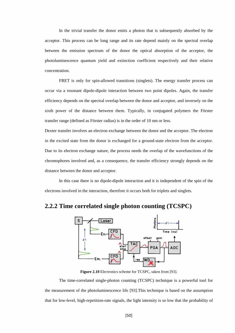
[50]
In the trivial transfer the donor emits a photon that is subsequently absorbed by the
acceptor. This process can be long range and its rate depend mainly on the spectral overlap
between the emission spectrum of the donor the optical absorption of the acceptor, the
photoluminescence quantum yield and extinction coefficient respectively and their relative
concentration.
FRET is only for spin-allowed transitions (singlets). The energy transfer process can
occur via a resonant dipole-dipole interaction between two point dipoles. Again, the transfer
efficiency depends on the spectral overlap between the donor and acceptor, and inversely on the
sixth power of the distance between them. Typically, in conjugated polymers the Förster
transfer range (defined as Förster radius) is in the order of 10 nm or less.
Dexter transfer involves an electron exchange between the donor and the acceptor. The electron
in the excited state from the donor is exchanged for a ground-state electron from the acceptor.
Due to its electron exchange nature, the process needs the overlap of the wavefunctions of the
chromophores involved and, as a consequence, the transfer efficiency strongly depends on the
distance between the donor and acceptor.
In this case there is no dipole-dipole interaction and it is independent of the spin of the
electrons involved in the interaction, therefore it occurs both for triplets and singlets.
2.2.2 Time correlated single photon counting (TCSPC)
Figure 2.10 Electronics scheme for TCSPC, taken from [93].
The time-correlated single-photon counting (TCSPC) technique is a powerful tool for
the measurement of the photoluminescence life [93].This technique is based on the assumption
that for low-level, high-repetition-rate signals, the light intensity is so low that the probability of
[51]
detecting one photon in one excitation pulse is less than 1, with a typical detection rate of 1
photon per 100 excitation pulses. During the measurements the sample is repetitively excited
with a pulsed light source (in the order of ps) with a high repetition rate. The system then
measures the delay time of each photon emitted by the sample under analysis against the
excitation pulse, and, after many cycles, it builds a probability histogram of the photons emitted
intensity versus time.
A typical example of a TCSPC electronic schematic is reported in figure 2.10. The
experiment starts with the excitation pulse (LASER) that simultaneously excites the sample (S)
and sends a signal to the electronics. The signal is passed through a constant fraction
discriminator (CFD), which accurately measures the arrival time of the two pulses. Then, the
signal coming from the electronic (“start” signal) passes through a to a time-to-amplitude
converter (TAC), which generates a voltage that increases linearly with time. As soon as a
photon is emitted by the sample (“stop” signal) the TAC is stopped. The arrival time of this
pulse is accurately measured using the CFD, which sends a signal to the TAC that now contains
a voltage proportional to the delay time between the excitation and the emission signals.
Eventually, the voltage is amplified by a programmable gain amplifier (PGA) and converted to
a numerical value by the analog-to-digital converter (ADC). The ADC stores each the value for
each events and finally the probability histogram is generated summing multiple “start” - “stop”
cycles.
A window discriminator (WD) acts as a filter for the generated voltage, suppressing all
the signals that does not fall inside a given range, and prevents false readings.
The instrument response function (IRF) of the instruments represents the instrumental
response with a zero lifetime emitting sample. It depends on the excitation pulse width and on
the timing accuracy of the electronic components.
The final histogram can be fitted by an exponential function to obtain the PL radiative
lifetime:
I(𝑡) = I0 + ∑ Ii𝑒−(𝑡
𝜏𝑖⁄ )𝑛𝑖=1 (27)

[52]
Where n is the number of exponential, I0 a background constant, Ii pre-exponential
factors and 𝜏𝑖 lifetime values. The system used in this thesis was an Edinburg Instruments F900-
red TCSPC, with pulsed laser-diode (λex = 371 nm) with a pulse width of ~60 ps and a cooled
photomultiplier tube coupled with a monochromator as detector.
2.3 Organo-Lead Halide Perovskites
The name perovskite identifies the family of minerals that can be described by the
generic formula ABX3; where A is the cation (Ca,Mg,Cs), B is a metallic cation (Ti,Pb,Sn.) and
X is the anion (O2-, Cl- I-;Br-). The Organo-Metal Halide Perovskite is obtained when in a
classical perovskite compound, A is replaced by organic cations, which often, thanks to its
reduced size, consists in methylammonium (CH3NH2). The ABX3 tetragonal perovskite-type
structure, illustrated in figure 2.11, consists of an extended framework of corner-sharing PbX6
octahedra (X can be typically Cl, I, Br, or a mix) with the methylammonium cation (MA,
CH3NH3+) occupying the central A site and surrounded by 12 nearest-neighbour halogen ions
[97, 98].
Figure 2.11Three-dimensional schematic representation of perovskite structure ABX3 (A = CH3NH3,B =
Pb, and X = Cl, I, Br), taken from [97].
The crystallographic stability [99] strongly depend on the size of the three ions and it
can be defined by two factors: the tolerance factor t [100], defined as the ratio between the
distance A-X to the distance B-X in an idealized solid-sphere model, and an octahedral factor μ,
defined as the ratio RB/RX [99]. In particular:
𝑡 = 𝑅𝐵+𝑅𝑋
√2(𝑅𝐴+𝑅𝑥) (28)

[53]
where RA, RB and RX are the ionic radii of A, B and X site elements. For halide
perovskites (X = F, Cl, Br, I), generally 0.81 < t <1.11 and 0.44 μ < 0.90 [99]. The ideal cubic
perovskite structure appears in a few cases for t-value very close to unity 1. The physical
properties of the perovskites depend crucially on the details of these distortions. For the
organic–inorganic halide perovskite, the cation A is the MA with RA = 0.18 nm, the anion X is a
halogen like I, Br and Cl (RX = 0.220 nm, 0.196 nm and 0.181 nm, respectively), usually in a
mixed halide material, and the cation B has universally been Pb (RB = 0.119 nm).
2.3.1 Perovskite-based photovoltaic devices
The generation of current in a solar cell, defined as the "light-generated current",
involves two key processes. The first process is the absorption of incident photons by the
photoactive material to create electron-hole pairs and then the separated charges have to be
collected.
Every solar cell is characterized by its short circuit current (Jsc) and its open circuit
voltage (Voc). The Jsc is the maximum photocurrent due to the direct connection of the opposite
contacts without any load between them, the second is the maximum potential applied (due to
an opportune load) to the cell for which the generated photocurrent (Jphoto) is perfectly balanced
by the dark current (J0), which is the diode leakage current density in the absence of light.
Subsequent to the absorption of photons there is the generation of photocurrent, where an
electron-hole pair is first generated and then separated and collected by the electrodes.
Figure 2.12 Equivalent electric circuit for a real solar cell.
In real cells, whose equivalent electric circuit is reported in figure 2.12, it is important
to take into account all the possible recombination channels due to presence of trap states,

[54]
defects or imperfect interfaces and that cause a diminishing of the net current. Such
recombination can be described as series resistance (Rs) and shunt resistance (Rsh). In particular,
Rs represents the resistance during the movement of current to reach the collecting zone and the
entity of Rs depending to mobility of the charges in the crossed mediums and their thickness.
Otherwise Rsh describes the quantity of charges that recombines before are collected. The entity
of both Rs and Rsh, depending to characteristics of crossed layer, as purity or intrinsic electronic
properties. The most fundamental equation that describes the behavior of solar cells is the diode
model:
𝐽(𝑉) = 𝐽𝑝ℎ𝑜𝑡𝑜 − 𝐽0𝑒[
𝑞(𝑉+𝐽𝑅𝑠)
𝑛𝑘𝐵𝑇−1]
−𝑉𝑅𝑠
𝑅𝑠ℎ (29)
where J is the current density measured at the cell electrodes, V is the voltage measured
across the cell, Jphoto is the photogenerated current density, J0 is the reverse saturation current
density, q is the elementary charge, Rs is the series resistance, Rsh is the shunt resistance, kB is
the Boltzmann constant, T is the absolute temperature, and n is the ideality factor.
Figure 2.13 J-V curve (in red) of a real device. The operating point with the maxima power is identified
by pair (Jmax; Vmax).
The performance of a photovoltaic device can be expressed in term of efficiency. In
particular, the external quantum efficiency (EQE) is the ratio of the number of carriers collected
by the solar cell to the number of photons of a given energy E incident on the solar cell and
therefore it is correlated to the Jsc:
𝐽𝑠𝑐 = 𝑞 ∫ 𝑠 𝐸𝑄𝐸 𝑑𝐸 (30)

[55]
where s is the incident spectrum, and q is the elementary charge.
Another way to indicate the performance of a photovoltaic is with the ratio between the
maximum output power (Pmax) and the power of the incoming irradiation (Pin), defined as the
power conversion efficiency:
𝜂 = 𝑃𝑚𝑎𝑥/𝑃𝑖𝑛 (31)
The electrical power delivered in every operating point is given by P = JV, whose
maximum (Pmax) occurs at specific potential Vmax and current Jmax (figure 2.13). In ideal case,
i.e. excluding both Rs and Rsh, these values correspond to Voc and Jsc
The difference between the real power Pmax that can be extracted by the solar cell and
the ideal power is the fill factor (FF):
𝐹𝐹 = 𝑉𝑚𝑎𝑥𝐽𝑚𝑎𝑥 𝑉𝑜𝑐⁄ 𝐽𝑠𝑐 (32)
As a consequence, the FF is affected by the series and shunt resistances, which in turn
are affected by the carrier mobility and balance, interface recombination, and film morphology
[101, 102].
A basic device structure of solar cell features an active layer, which is responsible of
absorbing the incoming light and generate the free charges, sandwiched between a transparent
and a metallic electrode. In particular, in the case of the perovskite-based solar cells, the devices
can be assembled in two different structures: the planar heterojunction and the meso-
superstructured. As shown in figure 2.14(a), the various layers for the latter are: the transparent
electrode (the anode), that most commonly is a layer of fluorinated-tin oxide (FTO) sputtered on
a glass substrate; the electron transporting layer (ETL) that consist in an oxide semiconductor
(e.g. titania) having a band alignment to favor the transfer of electrons to the anode; a
mesoporous oxide scaffold, to enhance light absorption due to scattering; the perovskite, i.e. the
light harvester medium that creates carriers following to the absorption of photons and finally
the hole transporting layer (HTL), that has specular activity with respect to electron transport
layer described before, and the metal contact. On the other hand, in a planar junction perovskite
solar cell (figure 2.14(b)), a several hundred nanometer thick absorber layer is sandwiched
between the ETL and the HTL without any mesoporous scaffold. Since the hybrid perovskite

[56]
has been shown to exhibit ambipolar charge transport [103], this architecture offers the
advantage that can be built in direct and inverted structures, i.e. with the transparent anode with
a structure like FTO/ETL/perovskite/HTL/metal, or with a transparent cathode, resulting in a
structure like FTO/HTL/perovskite/ETL/metal, respectively
Figure 2.14 (a) Schematic mesostructured device architecture (on the left) and cross-sectional SEM
image of the device structure, taken from ref. [98].The transparent electrode is the fluorinated-tin oxide
(FTO), on top of it there is a compact layer of titania (TiO2) and the mesoporous oxide. The perovskite is
the photoactive layers, and it is infiltrated into the mesoporous scaffold. Than the structure is capped with
the hole transporter (in this case it is the spiro-OMeTAD) and the cathode. (b) Cross-sectional SEM of a
planar heterojunction device. In particular this is the inverted architecture, with the transparent cathode
(ITO) in the bottom. Taken from ref. [104].
When a photon is absorbed by the perovskite, an exciton is generated and it propagates
just until the interface perovskite/ETL. At this point the exciton is separated into an electron and
a hole, which are collected respectively forward ETL and HTL. In order to have an optimal
exciton dissociation into free charges, the energy levels of the various layers have to be properly
aligned, such as the one showed in figure 2.15.
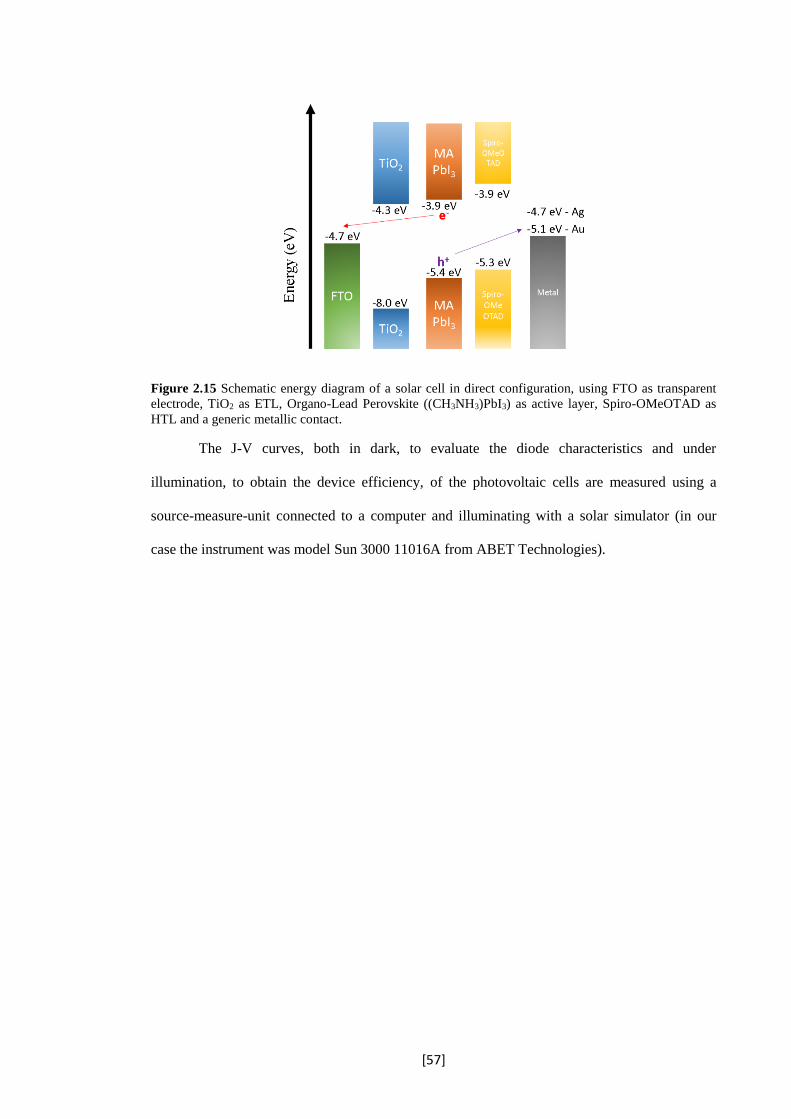
[57]
Figure 2.15 Schematic energy diagram of a solar cell in direct configuration, using FTO as transparent
electrode, TiO2 as ETL, Organo-Lead Perovskite ((CH3NH3)PbI3) as active layer, Spiro-OMeOTAD as
HTL and a generic metallic contact.
The J-V curves, both in dark, to evaluate the diode characteristics and under
illumination, to obtain the device efficiency, of the photovoltaic cells are measured using a
source-measure-unit connected to a computer and illuminating with a solar simulator (in our
case the instrument was model Sun 3000 11016A from ABET Technologies).
[58]
Chapter 3
Polymer-silicon hybrid photonic structures
In this chapter I report on the modification of the photoluminescence (PL) and decay
rates of a green-emitting commercial luminescent polymer (F8BT, poly[(9,9-di-n-
octylfluorenyl-2,7-diyl)-alt-(benzo[2,1,3]thiadiazol-4,8-diyl)]) infiltrated into one-dimensional
(1D) porous silicon photonic crystals (PS-PhCs), known as rugate filters, whose detailed inner
morphology I analyse with the help of (scanning) transmission electron microscopy, (S)TEM,
and scanning-electron microscopy, SEM, of focused ion-beam (FIB) milled sections. I observe
both suppression (in the stop-band) and enhancement (at the high-energy band-edge) of the
photoluminescence. Corroborating time-resolved measurements reveal a concomitant
modification of the emission lifetime that is enhanced at the band-edge and suppressed within
the stop-band, thus confirming a variation of the radiative decay rate of the excitations in such
hybrid organic-inorganic photonic nanostructures. I also find that the photonic stop-band is red-
shifted after polymer infiltration, due to the increased effective refractive index of the polymer-
infiltrated nanostructured system. The presence of just one unbroadened peak in the reflectance
spectra after infiltration suggests that infiltration extends for the whole depth of the rugate
filters. I assign the alteration of the emission of F8BT to the modification of the density of
photonic states within the photonic crystal. The following chapter is reproduced by permission
of Springer (see ref. [58]).

[59]
3.1 Hybrid photonic structures for light emission
modification
Photonic crystals provide perhaps the most powerful tool for manipulation of light
generation and propagation, thereby potentially enabling the implementation of photonics as the
most performing information and communication technology (ICT) platform. As such, PhCs
have been intensely studied over the last three decades especially with a view to combining
them with photoactive materials such as luminescent (macro)molecules and inorganic
semiconductors,[105, 106] or with plasmonic nanostructures, so as to achieve directional
modification of the fluorescence,[107-110] optically-pumped lasing,[67, 111] and optical
switching[112, 113] among other aims. In this context, microcavities have been widely used to
control and enhance the emissive properties of conjugated polymers [114-116]. Notably, porous
silicon-based PhCs, such as rugate filters [117], have attracted significant interest since they
provide a straightforward and technologically robust route to fabrication of optical
nanostructures with significant levels of complexity, while at the same time building on an
unrivalled silicon-based micro- and nano-technology. Indeed, this class of photonic systems has
been used widely for optoelectronic [118], photonic [119], sensing [5, 120] and biological
applications [121]. In particular, rugate filters are good candidates as vapor and liquid sensors
[122-124], and as detectors for biological activities such as proteases [125, 126].
Several ways to fabricate hybrid polymeric-inorganic structures have been reported in
the literature so far, but in most cases the preparation involved a “chemical approach”, namely:
the growth of the target macro-molecules “in situ” by chemically reacting smaller monomers
that can be easily infiltrated inside the pores [127]. This has been exemplified by either
electrochemical deposition [128, 129] or in-situ chemical polymerization [130] of suitable
monomers. Although the efficiency of such processes is relatively high (in terms of pore filling
and/or monomer conversion), the applicability of this method is limited to a relatively narrow
set of monomers, and therefore not generally applicable.

[60]
For this reason the preparation of hybrid Si-organic structures via a solution processable
method, i.e. by directly infiltrating the polymer inside the pores starting from a solution, is more
attractive [120]. This procedure requires a good optimization of the infiltration methodology to
successfully infiltrate the polymer inside the pores, especially if pore sizes are comparable to the
polymers gyration radii (typically a few nm), or to the size of aggregated/phase-separated
macromolecular meso-structures (up to tens of nm).
Electrochemically etched pores are in the tens to few hundreds of nm diameter,
depending on the etching parameters, thereby complicating the observation. However, gathering
details on the diameter and chemical nature (e.g. following partial oxidation) of the pores, is
particularly important with a view to infiltration of the latter with soft matter (e.g. luminescent
materials, but also, in perspective, biologically-active (macro)molecules).
Interestingly, I found that pore-clogging was not a particularly significant problem in
our hybrid PhCs obtained via infiltration of commercial poly(9,9'-dioctylfluorene-alt-
benzothiadiazole), F8BT (Mw ~ 46 kDa) into porous silicon. Upon infiltration I observe shifts
of the filters reflectance peaks that are consistent with coating of the inner walls of the pores to
the whole depth that can be probed in such optical experiments. I consider that the ability to
infiltrate the porous structures results from the particular relation between the limited polymers
gyration radius (Rg, of the order of few nm) and the minimum pore sizes (approximately 10
times as large as Rg) for which I obtain direct insight by means of electron microscopy.
Importantly, I find that the luminescence of the infiltrated macromolecular luminophore
is controlled by the photonic structure of the inorganic host, and shows an enhancement at the
high-energy end, and suppression at the low-energy end, of the photonic band. In general, I
consider that these polymer-infiltrated Si-based crystals powerfully exemplify an element of a
potential tool library of a “C-Si hybrid photonic platform”. Such a platform could be developed
for a multitude of applications, spanning from bio-sensors to high-capacity/high-speed data-
handling devices (e.g. for “Big-Data”), in a complementary or even alternative fashion to Si/III-
V hybrids.

[61]
3.2 Experimental details
Porous silicon rugate filters were prepared by Prof. G. Barillaro’s group in University of
Pisa, Information Engineering Department. Porous silicon rugate filters featuring a stop-band in
reflectance either in the visible or near-infrared range were prepared by electrochemical etching
of (100)-oriented, highly doped p-type silicon wafers (boron-doped, resistivity 0.0008–0.0012 Ω
cm, from Siltronix Corp.) in a 3:1 (by vol.) solution of 48% (by vol.) aqueous hydrofluoric acid
and ethanol (both from Sigma Aldrich). The electrochemical etching was performed in a home-
made Teflon cell using a two-electrode configuration, with the silicon substrate acting as anode
(working electrode) and a platinum ring immersed in the solution acting as cathode (and used as
pseudo-reference electrode). A source-measure unit (Keithley 2410 Source Meter) was used to
impose the desired etching current density and to monitor the voltage drop between the silicon
sample and the pseudo-reference electrode. The hydrofluoric acid solution was stirred during
the electrochemical etching so as to minimize hydrogen bubble formation on the sample surface
and enhance etching uniformity.
A cosine-shaped current density waveform with peak-to-peak dynamics from 13.3 to
39.9 mA/cm2, 50 repeats, and time period of 11 and 17.5 s was used to produce rugate filters
with a stop-band in reflectance centred at 551 nm and 827 nm, respectively before oxidation,
and shifting to 515 nm and 771 nm respectively after oxidation. Such an etching current density
waveform produces mesostructured porous silicon samples with periodic porosity (values
between 62.5 % and 69.5 %, with an average Pavg = 66%) and, in turn, with periodic refractive
index (oscillating between nmin = 1.69 refractive index units, RIU, and nmax = 1.93 RIU – neff =
1.81 @ 551 nm, yielding a maximum contrast of 0.26 RIU, and between nmin = 1.61 RIU, and
nmax = 1.83 RIU – neff = 1.72 @ 827 nm). I estimated the values of porosity and, in turn, of the
effective refractive index from the experimental reflectivity spectra of porous silicon layers
etched with constant current density of either 13.3 or 39.9 mA/cm2. These correspond to
minimum and maximum values of the cosine-shaped current density waveform used for rugate

[62]
filter etching, respectively, according to the procedure described in the work by Ruminski et
al.[122].
The effective refractive index has been determined by using the so called Bruggeman’s
model/equation. For the as-fabricated samples the effective refractive index has been calculated
simply by considering the porosity of the samples, instead, for the oxidized samples, it was
necessary to take into account a three component model, since I had to estimate the silicon
oxide fraction to obtain the best fitting with the reflectance spectra. [123].
To improve the infiltration process and prevent emission quenching by the heavily-
doped silicon layer, the rugate filters were partially oxidized into a tube furnace (ThermoLyne
21100) under pure-O2 (99.999%) at 600 °C for 30 min prior to infiltration.
F8BT infiltration into the cavities of the filters was obtained using a dip-coating
procedure [131] by first submerging the rugate filter into a toluene solution of the polymer, and
then by slowly extracting it. The procedure was carried out at a controlled lifting rate (0.01
mm/min) and temperature (29 °C). The excess polymer left onto the surface after dip-coating
was removed using a cotton swab soaked with toluene.
Normal incidence and angle-resolved reflectance spectra were collected with an Ocean
Optics S2000 spectrometer in combination with a fibre-coupled Ocean Optics HL-2000
tungsten halogen source. Steady-state angle-resolved photoluminescence measurements were
carried out by using a 405nm CW laser diode (Thorlabs) and an Andor Shamrock 163i
spectrometer coupled to an Andor Newton CCD camera cooled at -50 °C. Time-resolved PL
measurements were carried out with a time-correlated single-photon counting, TCSPC,
spectrometer (F900 Edinburgh instruments) with excitation provided by a pulsed laser diode
(λex = 371 nm, pulse-width ~ 60 ps).
FIB-SEM images have been taken by using a Carl Zeiss XB1540 “Cross-Beam”
focused-ion-beam microscope, whereas ion-beam milling of the samples was carried out using
Ar atoms. TEM-STEM images have been taken by using a Titan 80/300 TEM/STEM. This
instrument is fitted with a monochromator to deliver spatial/energy resolution capabilities of
0.14 nm/0.5 eV (monochromator off) and 0.3 nm/0.12 eV (monochromator on).

[63]
3.3 Morphological characterization
Figure 3.1 TEM/STEM images of rugate filter with reference peak (After infiltration) at 515 nm. (a)
Bright-field TEM image of the rugate filter (inset: photo of the same rugate filter). (b) bright-field STEM
overview image of the PhC (c) High Angle Annular Dark-Field zoom of the internal structure (d) SEM
image of a FIB-milled cross-section of the rugate filter at 515 nm detailing the pore structure, with pore
sizes on the order of 50 nm or so. Bright areas on the edge of the solid Si pillars are associated with
regions of more intense charging, and are thus assigned as rich in oxidised silicon, with a typical
thickness of 10 nm or so.
Figure 3.1 shows transmission electron microscope, TEM (a), and scanning TEM,
STEM (b, c), cross-sectional images of the rugate filters with “initial” (i.e. before oxidation)
stop-band at 551 nm, at different magnifications. Notably, the periodic modulation of the
porosity of silicon along the direction perpendicular to the surface can be clearly observed as
darker/brighter alternating regions in all TEM/STEM images (a, b, and c). The quality of the
“overview” figure 3.1(a) is good enough to enable counting the total number of layers (50) and
measuring the total thickness of the rugate filter (~ 7.6 μm). The sample has been covered with a
Pt layer (darker layer on the top of the structure) to protect the structure during the ion etching
carried out to obtain the slice for the TEM analysis. In figure 3.1(c) I report a zoomed-in STEM
image of the photonic structure, which shows a clear asymmetry in the bright and dark regions
in each period, thereby suggesting that the refracting index modulation is different from

[64]
sinusoidal, despite the sinusoidal etching current. I consider that this is likely due to current
density-dependent etching rates [132]. In figure 3.1(d) I report an SEM image of a FIB-milled
cross-section where it is possible to observe the inner part of the pores. Along their thickness I
note the presence of (somewhat discontinuous) brighter areas or spots that can be readily
associated to relatively insulating regions (charging up and therefore appearing brighter in the
images). The question arises as to whether such low-conductivity regions are to be identified
with the Si oxide or with the infiltrated polymer. It is possible to interpret such areas as the
oxidized inner layer of the cavities, because: (i) the “characteristic” thickness of 10 nm or so is
consistent with what expected on the basis of the oxidation parameters and with Bruggeman’s
modeling of the oxidized but not infiltrated filter, (ii) the shift of the reflectivity peak of the
filter upon infiltration (reported below) is only 12 nm or so, therefore consistent with a 2-3 nm
thick polymer layer (which we cannot detect at the resolution of this image).
The interplanar spacing D by inspection of figure 3.1(b), is ~ 150 nm, consistent with
the total thickness and the number of current periods. Such a value is further confirmed by 2-
dimensional Fast Fourier Transform (2D-FFT) analysis of figure 3.1(b) reported in figure 3.2).
The FFT peaks spacing is 6.67 μm-1 (corresponding to 150 nm). The presence of bright lines
denotes a high uniformity of the (vertical) periods over the entire surface of the slice, but a
much lower uniformity of the pillars and pores dimension.
Figure 3.2 2D-FFT transform (inset: frequency profile extracted from the 2D-FFT, the distance between
the lines is found to be 6.67 μm-1).
I also analyzed the structure of figure 3.1(a) along its depth at higher magnification. In
figure 3.3 I present two TEM cross-sections taken at the same magnification (12000

[65]
magnifications) in the top (a) and in bottom (b) section of the rugate filter. Despite some small
oscillations in the layers in the top part of sample, the interplanar distances appear nearly
perfectly matched in both parts, as highlighted by the two parallel dashed lines. The only
exception is the very last layer etched (in the bottom part of the sample) which is smaller than
the other ones.
Figure 3.3 Bright-field TEM images taken at 12000 magnifications with 0.5 s exposure in the top and
bottom part of the rugate filter.
3.4 Optical characterization
In figure 3.4 I report the reflectance spectra of both rugate filters (i.e. tuned (a) and
detuned (b)) before (red line) and after the dry oxidation process (blue line). For the tuned
sample (figure 3.4(a)), the reflectance peak is blue-shifted by ~33±1 nm due to the formation of
an oxide layer and, in turn, a different effective refractive index. This is also confirmed by the
lowering of the total reflectance induced by the lowering of the dielectric contrast. Considering
this blue-shift and the determination of the interplanar spacing via STEM imaging analysis,
according to the Bruggeman’s equation, the silicon oxide fraction formed during the oxidation
process should be ~10 nm. For the rugate filters with initial (i.e. before oxidation) stop-band at
827 nm (figure 3.4(b)) the blue-shift of the reflectance peak is about 56 nm. The intaplanar
spacing D is found to be ~240 nm and it has been evaluated by the reflectance measurements
and taking into account the thickness of the oxide determined for the “green” rugate filter.

[66]
Figure 3.4 Reflectance spectra of the tuned (a) and detuned (b) rugate filter before (red line) and after
(blue line) the oxidation process.
To determine the effect of the photonic structure on the F8BT spectrum I compared the
optical properties of the filter with the stop-band centred at 515 nm (after oxidation, red-shifting
by about 12 nm upon infiltration, thus providing significant spectral overlap with the F8BT PL,
and hence referred to as “tuned” filter) with those of the “detuned” filter (stop-band centred at
771 nm, after oxidation, further red-shifting upon infiltration) that is used as a reference.
Figure 3.5 (a) PL spectrum of a neat film of F8BT on a compact silicon substrate, and (b and c)
reflectance spectra for the PhCs before (blue) and after polymer infiltration (red). The infiltration leads to
a red-shift of the photonic stop-band (and thus of the reflectance peak) of about 12±1 nm. Note that the
vertical scales for (b) and (c) are different, i.e 40% and 100% reflectance, respectively. Inset: cartoon
illustrating the inferred cross-section of the rugate filter (D is the inter-planar spacing determined by the
period of the anodic etching current); the polymer layer is not filling the pores of the rugate filters, but
there is just a layer on the walls of the cavities (see main text for discussion). The structure of the sample
used to measure the F8BT PL is also shown.

[67]
Figure 3.5 shows the typical PL spectrum of an F8BT film (panel a) and the reflectance
spectra for tuned (panel b) and detuned samples (panel c) before and after the infiltration of the
F8BT, at normal incidence. I could not detect any PL from the bare porous silicon for both
tuned and detuned samples.
Upon polymer infiltration the reflectance peaks red-shifted by ~ 12±1 nm in both
samples due to the increased effective refractive index. In particular the reflectance peak for the
tuned sample red-shifted from 515 nm to 526 nm after infiltration and for the detuned one it red-
shifted from 771 nm to 784 nm. This is in qualitative agreement with the prediction of the
Bragg-Snell law (Eq. 17), which can then be used to quantify the effective refractive index neff
[133].
From Eq. 17, I determine neff = 1.81 and 1.72 for the as-fabricated rugate filters, for
interplanar spacing D of 150 nm and 240 nm as obtained from TEM images for the rugate with
stop-band peaks (before oxidation) at 551 nm and 827 nm, respectively.
As a further check, the total thickness (t) of the nanostructured samples can also be
calculated by using the interference fringes in the reflectance spectra once the effective
refractive index of the photonic crystal is known:
eff
fringes
n
Nt
2 (33)
where Nfringes is the number of fringes within the spectral range ν (in cm-1). By using
the effective refractive indices obtained with the Bragg-Snell’s law, and a spectral range of
~4800 cm-1 for the tuned sample and ~3000 cm-1 for the detuned one, I found t = 7.6 μm for the
tuned filter (which is in excellent agreement with the SEM/TEM observations) and t = 12 μm
for the detuned one.
Considering that the refractive indices of F8BT are 1.6 (extraordinary one) and 1.8
(ordinary one) [134] and the refractive index of air is 1, I would have expected a spectral shift of
the reflectance peaks bigger than the observed one if the cavities had been completely filled by
the polymer. In fact, in the case of a complete filling of the cavities with the F8BT (i.e. totally
removing the contribution of the air to the effective refractive index and replacing that with the

[68]
one of the polymer in the Bruggeman’s model) the reflectance peaks of the two rugate filters
would have moved from 515 nm to 634 nm (119 nm shift) and from 771 nm to 960 nm (189 nm
shift) for the tuned and detuned filter, respectively.
Having established that infiltration leads to a “coating” of the pores walls, rather than to
“solid filling” of the pores with the polymer, an interesting question arises as to whether such a
“coating” is complete or partial in the vertical direction. In fact, partial “coating” of the pores is
excluded by the SEM and (S)TEM micrographs (figure 3.1), that do not show any such
evidence, and by the optical measurements providing evidence for just one un-broadened
reflectance peak [135]. In fact, partial filling/coating along the pore’s depth should have resulted
in two reflectance peaks as in the presence of two PhCs stacked one over the other: the one
made by Si and air and the one made by Si/polymer and air [136]. Since the shift of the
reflectance peak upon infiltration is 12±1 nm, any such a peak should be clearly observable in
the overall reflectance spectrum, unless the one associated to the “empty” fraction of the pores
is particularly small compared to the other. In practice, given the intensity resolution with which
I was able to measure the spectral features, I can estimate that the pores are coated to well over
99% of their depth.
To observe the modification of the PL spectra induced by the photonic crystal, I
compared the PL of the F8BT infiltrated into the tuned and detuned (reference) filters, to avoid
those small differences in the surface chemistry of the porous silicon samples affected the
determination of the photonic effects. The PL spectra were then normalized with respect to the
intensity at λ = 550 nm, i.e. several tens of nm away from the centre of the photonic stop-band
[136].
In Figure 3.6(a) I report the PL spectra as a function of the angle of incidence of the
exciting laser beam for both tuned and de-tuned infiltrated filters (only at normal incidence for
the detuned sample, as there is no angular dependence). Clearly, F8BT’s photoluminescence is
strongly modified by the presence of both the stop-band and of the interference fringes, which
contribute both to “structuring” the emission. Remarkably, the PBG suppresses (albeit partially)
propagation at 528 nm (at 0 incidence) and increases the intensity at the high-energy edge

[69]
(from 518 nm at 0° incidence to 503 nm at 30° incidence). This is in agreement with the
expected suppression of the photonic density of states (DOS) in (the middle of) the stop-band,
and with its increase at the stop-band high-energy edge [137] and it will be demonstrated below
by mean of radiative lifetime measurements. Such enhancement and the suppression display
strong dependence on the excitation angle, because of the dispersion of the stop-band.
Figure 3.6 (a) PL spectra (solid lines) collected at different incidence angle (from 0° to25° with step of
5°) of the exciting beam for F8BT infiltrated into the tuned PhC and at 0° for the F8BT infiltrated into the
detuned PhC (dashed line). I used a CW laser, emitting at 405 nm, as excitation source. I can observe the
PL peak dispersion moving from 518 nm at 0° to 506 nm at 25°. (b) Ratio between the PL spectra from
the tuned and detuned PhC at different angles, as in (a) above.
The enhancement/suppression above is appreciated clearly in Figure 3.6(b) in which I
have plotted the ratio (Rn) between the PL spectra of infiltrated tuned filter and detuned filters.
Thus figure 3.6(b) emphasises both enhancement (Rn > 1) in the region between 518 and 506
nm and a minor suppression (Rn < 1) at the stop-band (between 528 and 512 nm) for angle
increasing from 0° (normal incidence) and 25°. The difference in the intensity of the
suppression and enhancement could be explained as the difference in the experimental set-up
for the two samples (film thickness, laser spot size) and to refractive-index effects [138].

[70]
Figure 3.7 Radiative decay of the F8BT PL measured by time-correlated single-photon counting, TCSPC
(371 nm excitation) and recorded either within the stop-band (528 nm, top panel) and at the high-energy
edge (518 nm, bottom panel) for a neat F8BT film on Si, as well as for F8BT infiltrated into the tuned and
detuned filters, as indicated in the plots legends.
Finally, to obtain conclusive evidence about the modification of the radiative rate of
F8BT induced by the “photonic host” (i.e. the rugate filters) I measured the PL temporal decay
(figure 3.7) both within the stop-band (528 nm) and at the high-energy edge of the latter (518
nm). I focused on these two spectral lines because at such wavelengths there is a clear
modification of the DOS.
The results for a neat F8BT film (thickness ~ 800 nm) on Si deposited by dip-coating,
are in good agreement with previous works [139-142] showing a mono-exponential PL decay
for neat films of F8BT deposited by spin-coating, with lifetimes varying from 0.89 to 1.84 ns
depending on wavelength, film thickness and substrate materials. In this case, I obtained decay
times of ~ 1.15 ns at 518 nm and ~ 1.18 ns at 528 nm, table 3.1). However, when the polymer is
infiltrated in the tuned and detuned PhCs, I find that accurate fits of the PL temporal decay can
only be obtained with a “bi-exponential” equation [60], with characteristic lifetimes as reported
in table 3.1 below.
The need for a bi-exponential fit for the infiltrated polymer is not surprising, given the
large area/volume ratio of the regions in which the polymer is accommodated, and for which a
relatively strong interaction with the SiO2/porous silicon can be expected, both of a chemical
and of a physical nature which are likely to lead to different strand packing patterns and likely

[71]
formation of weakly-bound interchain states in addition to the monomolecular singlet excitons
that characterise the emission of the neat thin films. In general, the photoluminescence of
conjugated semiconductors is a sensitive probe of their chemico-physical environment, and of
the geometry adopted by the polymeric strands. Similar effects have been noted both when
adsorbing similar chromophores on nanospheres in three-dimensional self-assembled opals[110]
or in the presence of strong interchain interactions for a variety of conjugated polymers,
including F8BT [143, 144]. While such interactions might differ significantly for the infiltrated
F8BT with respect to the one on neat Si, they should be very similar for the tuned and detuned
filters, thereby enabling a meaningful comparison.
τ1 (ps)(I1) τ2 (ps) (I2) High-energy edge
Tuned PhC 690±34 (0.8) 1210±60 (0.2) Detuned PhC 830±41 (0.95) 1590±79 (0.05)
Film on Si 1150±57 Stop-band Tuned PhC 860±43 (0.94) 1680±84 (0.06)
Detuned PhC 830±41 (0.95) 1600±80 (0.05) Film on Si 1180±59
Table 3.1 Temporal decay constants (τ1, τ2) extracted from least square fits of the PL decay curves with
their relative weight (I1, I2).
It is thus very interesting to observe a very clear reduction of both lifetimes (table 3.1)
at the high-energy edge of the stop-band (518nm) for the tuned with respect to the (detuned)
reference filter (~17% of τ1 and ~24% τ2 for the mean). As expected, I also find slightly longer
time constants within the stop-band (528 nm) (by ∼4% for τ1 and ~5% for τ2). Note also that
the less significant variation within the stop-band (effectively comparable with the error) is fully
consistent with a much less important suppression of the emission in this region, as compared to
the enhancement at the band edge (as also evidenced by figure 3.6). Such apparently limited
differences between the radiative decay rates of F8BT within tuned/detuned filters are entirely
within expectations for one-dimensional (1D) photonic structures such as rugate filters, that
only provide intrinsically limited “photonic confinement” (i.e. only along the z-direction) and
that a narrow spectral width (516 – 533 nm) compared to the PL of the F8BT guest (490 – 700
nm) [145].

[72]
3.5 Conclusion
In conclusion I have investigated a hybrid silicon-organic photonic system. I achieved
excellent infiltration of the green-emitting highly luminescent F8BT into rugate filter cavities
whose detailed nano-/meso-structure I carefully analysed via (S)TEM and SEM. F8BT
infiltration into the rugate filters leads to a red-shift of the stop-band and brings about a
wavelength- and angle-dependent PL suppression-enhancement due to the presence of the
photonic stop-band. A modification of the emission lifetime at the stop-band high-energy edge
is clearly observed and assigned to the modulation of the photonic density of states imposed by
the conjugated polymer.

[73]
Chapter 4
Spectroscopy of synthetic opals
In this chapter I present a spectroscopic investigation of a particular class of 3D
photonic crystals, synthetic opals. In particular, I describe a simple bottom-up approach for
preparing photonic crystals from a water suspension of polystyrene microspheres and how to
introduce supramolecularly engineered luminescent polymers to observe suppression-
enhancement in their photoluminescence spectrum. Secondly I present transmission experiment
to explore the Bragg-Snell’s law for the determination of the effective refractive index.
The following chapter is reproduced by permission of AIP Publishing LLC., Copyright
2016 (see ref. [110]) and of American Association of Physics Teachers (see ref. [146]).
4.1 Synthetic opals
Even though PhCs are mainly prepared by top–down methods, the bottom–up approach
seems very promising in order to tailor the system for specific applications [147]. In this
scenario, colloidal photonic crystals, e.g synthetic opals [148] (figure 4.1), are very interesting
due to their low fabrication cost and ease of preparation.
Figure 4.1 SEM image of the opal structure (left) and photo of opals made with different microspheres
diameter (right), the diameter (in nm) is indicated below the opals. The reflected color changes as
function of the dimension, according to Bragg-Snell’s law.

[74]
Opals are in fact a versatile system that can enable the investigation of a variety of
photonic effects and especially the fine-tuning of optical properties [149], including the
modification of the emission spectra and radiative rates [110], optical switching [150], and
hybrid photonic-plasmonic like resonances [113]. Different active materials such as metal
nanoparticles [151], semiconductor nanocrystals [152] or conjugated molecules [153], can be
effectively incorporated into the opals in by means of infiltration, co-growth or evaporation.
Opals are 3D photonic crystals assembled in a face-centred-cubic (FCC) structure of
dielectric microspheres (figure 4.1). Such structures can be prepared by many bottom-up
approaches, exploiting the spontaneous assembly of the micospheres into the crystalline
structure. The dielectric contrast of the media composing the opals is given by the refractive
index of air (n = 1) and of the material used for the microspheres.
To evaluate the effective refractive index of the opals, but more in general of a PhCs, I
can use Lorentz-Lorenz equation [153]:
𝑛𝑒𝑓𝑓2 −1
𝑛𝑒𝑓𝑓2 +2
= ∑ 𝑓1𝑛1
2−1
𝑛12+2
+ 𝑓2𝑛2
2−1
𝑛22+2
(34)
Where neff is the effective refractive index, n1 is the refractive index of vacuum (n1=1),
n2 is the refractive index of the material used and f1&2 the volume fractions of the two media. In
particular, f2 = 0.74 for a face-centred-cubic structure.
As reported in figure 4.2, opals cannot have a complete photonic band-gap (i.e. a
photonic gap for all the values of k) even with extremely high dielectric contrast, but only a
stop-band along the crystallographic direction (111) (normal to the growth direction, fig. 3.2),
which is also called pseudo-photonic band gap (p-PBG).
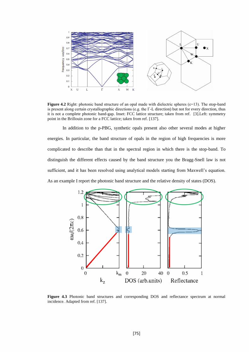
[75]
Figure 4.2 Right: photonic band structure of an opal made with dielectric spheres (ε=13). The stop-band
is present along certain crystallographic directions (e.g. the Γ-L direction) but not for every direction, thus
it is not a complete photonic band-gap. Inset: FCC lattice structure; taken from ref. [3].Left: symmetry
point in the Brillouin zone for a FCC lattice; taken from ref. [137].
In addition to the p-PBG, synthetic opals present also other several modes at higher
energies. In particular, the band structure of opals in the region of high frequencies is more
complicated to describe than that in the spectral region in which there is the stop-band. To
distinguish the different effects caused by the band structure you the Bragg-Snell law is not
sufficient, and it has been resolved using analytical models starting from Maxwell’s equation.
As an example I report the photonic band structure and the relative density of states (DOS).
Figure 4.3 Photonic band structures and corresponding DOS and reflectance spectrum at normal
incidence. Adapted from ref. [137].

[76]
In figure 4.3 three distinct photonic regions are shown: in red band structure exhibits a
linear regime, corresponding to a constant DOS; the band gap is highlighted in blue and in
correspondence the DOS is suppressed and, finally, the band structure, that is circled in green,
has a non-linear dispersion and presents critical points, also known as van Hove singularities (in
analogy to the critical points in the joint density of states commonly used for describing the
optical properties of semiconductors [154]) and this correspond to a divergent DOS. The
photonic band-gap and the singularities are caused by different physical phenomena.
Respectively, the PBG is due to backward diffraction by the (111) planes, the van Hove
singularity are caused by diffraction along directions different from the incident one, by families
of planes other than the (111). This difference has a strong impact on the dispersion properties
of the two structures as shown in figure 4.4.
Figure 4. 4 Density of states at different angles and for different orientations. Taken from ref. [137].
In figure 4.4 it can also be observed observe that the stop-band and the van Hove
singularities have opposite trends as function of the angle of incidence (θ). In fact, by increasing
θ of the gap shifts to higher energies whereas the singularities move at lower energies.
Furthermore, the dispersion of the van Hove singularities depends on the orientation of opal.

[77]
4.2 Polyrotaxanes
Conjugated polyrotaxanes [143, 155, 156] are a special class of conjugated polymeric
semiconductors that are threaded through cyclodextrin macrocycles which act like rings around
the conjugated backbone (figure 4.5) .These rings behave as “spacer” between the chains and
thus provide control over the interchain interactions and enabling us to investigate the
photophysics of conjugated semiconductors [157, 158].
Figure 4.5 Chemical structures of the cyclodextrin-threaded conjugated polyrotaxanes with poly(4,4’-
diphenylene-vinylene) (PDV.Li) core with naphthalene stoppers (average number of repeat units n = 10)
and its optical properties (photoluminescence quantum efficiency, PLQE, and OLES external quantum
efficiency, EQE) as function of the threading ratio. Reproduced from ref. [157].
In particular, cyclodextrin insulation suppresses intermolecular interactions, showing
photoluminescence decay dynamics which is independent of concentration [156, 159].
Interestingly, although encapsulation preserves the intrinsic spectroscopic properties of
the isolated chains, it does not suppress the charge transport in solid films, thus yielding
enhanced and blue-shifted electroluminescence with respect to unthreaded conjugated polymers.
For all these reasons, during the last 15 years they have been successfully used in white-
light-emitting diodes [6-8] and optically pumped laser [9, 10].
Another interesting property of polyrotaxanes is their water solubility. In fact,
cyclodextrin threading is obtained via hydrophobic binding, which requires processability in
polar solvents. For this reason, polyrotaxanes backbones are functionalized with of polar groups
and are thus interesting for a variety of applications, spanning from biosensing to incorporation
into plastic photonic structures without the need of covalently binding the polymers.

[78]
4.3 Experimental details
I prepared opals with polystyrene microspheres of different size. The preparation of the
artificial opals consist in a self-assembly of commercial polystyrene microspheres (Duke
Scientific, 10% in volume, diameters of 200, 220, 370 and 430 nm, standard deviation < 5%;
refractive index, nPS = 1.59), exploiting the vertical deposition method onto glass substrates.
The starting suspensions are further diluted to 0.2% v/v in diluted water in order to
grow opals of the desired thickness. Typically, an opal thickness of 3-4 μm offers the best
compromise between reflection and transmission. The opals have been prepared onto
commercial soda lime slides previously cleaned with the RCA-1 procedure to obtain a more
hydrophilic surface [160].
Once cleaned, the slides are immersed perpendicularly in the suspension of
microspheres and lifted at a constant speed (7x10⁻⁵ mm/s) at 28 °C. The process takes place
inside an incubator placed onto an optical table to avoid any possible vibration that would cause
defects and stacking faults inside the photonic structures. I used a home-built dip-coater with a
motorized translation stage (Thorlabs). The opal film is created at the interface between the
water meniscus and the glass substrate by the Van der Waals force during water evaporation
(figure 4.6(a)). The polystyrene microspheres self-assemble into a face-centered cubic lattice
with the crystallographic [111] direction oriented perpendicular to the substrate. Figure 4.6(b)
shows the dip-coater inside the incubator with multiple slides securely attached to an extension
that permits to simultaneously create opals of different sized microspheres.
Figure 4.6 (a) Scheme of the vertical deposition technique used to prepare the opals and (b) the
experimental set-up.

[79]
The active material I used was a semiconducting polymer, PDV.Li, a polyelectrolytic
derivative of polypara-phenylene where sulfonated sidegroups are balanced by Li+ ions,
threaded with β -cyclodextrin macrocycles (PDV.Li⊂ β –CD), known as polyrotaxanes (figure
4.5) [156]. I used of PDV.Li⊂β–CD with threading ratio 2 (i.e. number of cyclodextrins per
monomeric repetition unit). The conjugated polymers were synthesised at the “Chemistry
Research Laboratory, Department of Chemistry, University of Oxford” by Dr. Shane O.
McDonnel and Prof. Harry L. Anderson.
I obtained effective incorporation of the polyrotaxane inside the opals via a co-growth
method during the vertical deposition of the PhC. A PDV.Li⊂β–CD concentration of 8x10⁻³
mg/ml yielded homogeneously infiltrated opals without hindering the formation of the photonic
crystals (which could affect the intrinsic PhC optical properties) while preserving strong PL
properties of the system. Furthermore, partial infiltration of voids preserves a reasonable
dielectric contrast within the structure, as inferred from lack of spectral shifts and narrowing
(broadening) of the stop-band. Scanning electron microscope (SEM) micrographs of the co-
grown PhCs reported in figure 4.7 show no presence of lattice distortion induced by the
incorporation of polyrotaxanes, nor an excess polymer layer on the opal surface for co-grown
PhCs with 8×10⁻³ mg/ml PDV.Li⊂β-CD solution and, more importantly, that the interstices
between nanospheres are empty, thereby preserving a desirable higher dielectric contrast within
the structure than otherwise possible in case of substantial filling of the interstices. The inset of
figure 4.7(a) shows a photography of the opal with a laser diode (λ = 405 nm) incident on the
crystal surface. I can observe the hexagonal diffraction pattern of the infiltrated opal, thus
confirming the high internal order of the FCC crystal [161, 162].

[80]
Figure 4.7 SEM micrographs of an opal film incorporating PDV.Li⊂β-CD: (a) cryo-cleaved wall surface
showing the internal structure of the opal, (b) film cross-section. Strong contrast between the sphere and
the interstices is observed, confirming that the latter are not filled up by the conjugated polyelectrolytes
(the density of the conjugated moiety and of the spheres being comparable). Inset: Photography of the
diffraction pattern from the opals. Images were collected using the SEM mode of a dual beam Carl Zeiss
XB1540 “Cross-Beam” focussed-ion-beam microscope and the cross section was obtained via cryo-
cleaving an opal film. Adapted from ref. [110].
Normal reflectance and angle resolved transmittance measurements have been carried
out using an Ocean Optics S2000 spectrometer in combination with a fibre-coupled Ocean
Optics HL-2000 tungsten halogen source. Steady-state PL spectra at different incidence angle of
the exciting beam have been carried out using a pulsed laser diode (λex = 371 nm, pulse width
~60 ps) and an Andor Shamrock 163i spectrometer coupled with an Andor Newton CCD
camera cooled at -50 °C. Samples have been mounted on a rotating stage (M-060.DG, Physik
Instrumente, resolution ~0.0001°).
4.4 Bare opals investigation
The obtained synthetic opals have an area of 2 cm2 and to check the crystals
homogeneity normal incidence reflectance spectra have been collected in different spots of the
samples. Figure 4.8 shows the reflection spectra for the opals made with spheres having a
diameter of 200 nm (a), 220 nm (b) 370 nm (c) and 430 (d).

[81]
Figure 4.8 Reflectance spectra collected from opal made with microspheres with a diameter of (a) 200
nm, (b) 220 nm, (c) 370 nm and (d) 430 nm. Inset: scheme of the mapping.
In all spectra I observed the presence of three characteristic structures: the Bragg
reflectance peak (except for the opal made with larger spheres, where this peak is in the “deep”
NIR and thus not visible using the spectrometer available in our laboratory) at 450 nm, 500 nm
and 825 nm for the sample made with spheres of 200 nm, 220 nm and 370 mn diameter,
respectively; the interference fringes due to the Fabry-Perot effect from the front and back faces
of the crystal and the van Hove-like modes 420 nm and 470 nm for the opal made with 370 nm
spheres and 480 nm and 540 nm for the opal made with 430 nm sphere. The latter are situated at
shorter wavelengths than the Bragg peak and are known to depend strongly on the internal FCC
order [109, 137] and on the microsphere quality [109]. According to the Bragg-Snell’s law, the
Bragg peak shifts to lower energies while increasing the diameter of the microspheres.
Interestingly, the spectral position and the spectral shape of the Bragg peak and van Hove
singularities are unchanged in each point of the samples, thus suggesting a good uniformity in
the PhCs.

[82]
Figure 4.9 Reflectance (blue line) and transmittance (red line) spectra of an opal prepared with
microspheres diameter = 220 nm.
Figure 4.9 shows the reflectance and transmittance spectra of the opal prepared with
microsphere having a diameter of 220 nm. The photonic band-gap can correspond to a
reflectance peak and a transmission dip. I calculated the total thickness of the opals using the
interference fringes in the reflectance spectra using Eq. 18 and the neff obtained from Eq. 19.
The values calculated from the opals shown in figure 4.8 are reported in table 4.1
Microspheres diameter (nm) Thickness (μm)
200 2.9±0.2
220 3.1±0.1
370 2.6±0.1
430 4.2±0.2
Table 4.1 Thickness of the opals made with different micorspheres diameters.
As seen from table, it is possible to achieve a good control on the total thickness
of the sample.
Angle resolved transmittance measurements permits to analyze the dispersion
(i.e. the dependence of the photons on the wave-vector of the light) of the photonic gap
and the high-energy modes. In fact, as observed in the band structure of opals (figure
4.4) there is a strong dependence on the wave vector k which is correlated to the angle of
incidence of light θ. In particular, I can sample along the LU crystallographic direction.

[83]
Figure 4.10 Angle-resolved transmittance spectra for the opal made with microspheres diameter 430 nm
for (a) p- and (b) s-polarised light.
Figure 4.10 shows the transmission spectra collected with p- (a) and s- (b) polarised
light of an opal made with spheres with a diameter of 430 nm.
As previously said, the Bragg peak cannot be resolved at normal incidence, similarly to
the reflectance spectra shown before in figure 4.8(d). Interestingly, the stopband starts appearing
at 40°, as predicted by the Bragg-Snell’s law, the stopband blue-shifts at higher incidence angle.
The minimum in the transmission spectrum increases for p-polarized light as the incident angle
approaches Brewster’s angle. In addition to the photonic stop-band I can observe the high-
energy modes. Such structures have opposite dispersion compared to the photonic gap and
therefore undergo to a red-shit while increasing the collection angle. To show better the
dispersion of the photonic bands, the same data are reported on colored contour-plot in figure
4.11.
Figure 4.11 Colored contour-plot of the transmittance spectra for the opal made with microspheres
diameter 430 nm for (a) p- and (b) s-polarised light. Transmittance percentage is shown in color scale.
Although limited to higher angle, I can observe that the dispersion of the photonic gap
that is the same for both polarizations, whereas the width of the stopband is rather different, in
particular for polarization p the peak narrows increasing the angle of incidence, while for the s
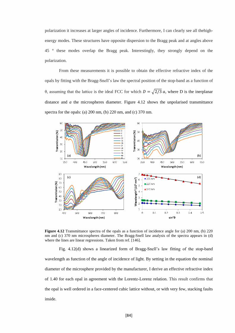
[84]
polarization it increases at larger angles of incidence. Furthermore, I can clearly see all thehigh-
energy modes. These structures have opposite dispersion to the Bragg peak and at angles above
45 ° these modes overlap the Bragg peak. Interestingly, they strongly depend on the
polarization.
From these measurements it is possible to obtain the effective refractive index of the
opals by fitting with the Bragg-Snell’s law the spectral position of the stop-band as a function of
θ, assuming that the lattice is the ideal FCC for which 𝐷 = √2/3 𝑎, where D is the inerplanar
distance and a the microspheres diameter. Figure 4.12 shows the unpolarised transmittance
spectra for the opals: (a) 200 nm, (b) 220 nm, and (c) 370 nm.
Figure 4.12 Transmittance spectra of the opals as a function of incidence angle for (a) 200 nm, (b) 220
nm and (c) 370 nm microspheres diameter. The Bragg-Snell law analysis of the spectra appears in (d)
where the lines are linear regressions. Taken from ref. [146].
Fig. 4.12(d) shows a linearized form of Bragg-Snell’s law fitting of the stop-band
wavelength as function of the angle of incidence of light. By setting in the equation the nominal
diameter of the microsphere provided by the manufacturer, I derive an effective refractive index
of 1.40 for each opal in agreement with the Lorentz-Lorenz relation. This result confirms that
the opal is well ordered in a face-centered cubic lattice without, or with very few, stacking faults
inside.
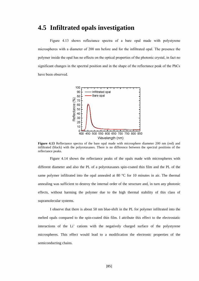
[85]
4.5 Infiltrated opals investigation
Figure 4.13 shows reflectance spectra of a bare opal made with polystyrene
microspheres with a diameter of 200 nm before and for the infiltrated opal. The presence the
polymer inside the opal has no effects on the optical properties of the photonic crystal, in fact no
significant changes in the spectral position and in the shape of the reflectance peak of the PhCs
have been observed.
Figure 4.13 Reflectance spectra of the bare opal made with microsphere diameter 200 nm (red) and
infiltrated (black) with the polyrotaxanes. There is no difference between the spectral positions of the
reflectance peaks.
Figure 4.14 shows the reflectance peaks of the opals made with microspheres with
different diameter and also the PL of a polyrotaxanes spin-coated thin film and the PL of the
same polymer infiltrated into the opal annealed at 80 °C for 10 minutes in air. The thermal
annealing was sufficient to destroy the internal order of the structure and, in turn any photonic
effects, without harming the polymer due to the high thermal stability of this class of
supramolecular systems.
I observe that there is about 50 nm blue-shift in the PL for polymer infiltrated into the
melted opals compared to the spin-coated thin film. I attribute this effect to the electrostatic
interactions of the Li+ cations with the negatively charged surface of the polystyrene
microspheres. This effect would lead to a modification the electronic properties of the
semiconducting chains.

[86]
Furthermore, due to the preparation method, that induces strong capillary forces [163],
and to the internal geometry of the crystal, the polymers undergo to structural constraints,
leading to a modification of the PL dynamics of the polyrotaxane compared to that observed in
a neat-polymer film or solution [157].
Figure 4.14 Normalized reflectance spectra (coloured lines) of the bare opals and normalized PL
emission (black solid line) of polyrotaxanes inside a thermally annealed opal and of a spin-coated thin
film (black dashed line). The annealing was necessary to keep the material chemical properties but
avoiding the photonic contribution.
The main results discussed here concern spheres with a diameter a = 200 nm since these
ensure an optimal spectral overlap of the polyrotaxane PL spectrum and of the opal stop-band.
Figure 4.15 PL (black), reflectance (red) and transmittance (green) spectra col lected at normal incidence
for spray-coated opals made with beads having diameter 200 nm (a) and 430 nm (b).

[87]
Figure 4.15 shows reflectance and transmittance spectra of the opal made with
polystyrene microspheres with a diameter of 200 nm. As expected, the reflectance peak at ~450
nm corresponds to a minimum in the transmittance spectrum. Remarkably, the PL emission is
strongly modified by the opals. Specifically, in correspondence of the photonic stop-band there
is partial suppression of the PL, whereas there is an enhancement at the high-energy edge.
The angle-resolved PL spectra for infiltrated opal are reported in figure 4.16. In
particular, the spectra as function of the illumination angle (a) and the PL ratio between the
emission from the polyrotaxanes infiltrated into the as prepared opal and the melted one (b) are
shown.
The PL of the polyrotaxanes is strongly modified by the photonic crystal: in particular,
the emission is partially suppressed in correspondence of the stop-and. In addition, there is an
enhancement of the PL intensity at the high-energy edge of the stop-band. Both enhancement
and suppression have the same dispersion as the stop-band, thus suggesting that both effects are
connected to a directional redistribution of the photonic density of states [7, 13].
The enhancement/suppression effects are better appreciated in the ratio between the two
PL spectra (figure 4.16(b)). Note that within the PBG the ratio is lower than 1 (indicated in the
figure by the black line), instead the ratio is above 1 for the short-wavelength edge of the PBG
[7, 13, 15, 16].
Figure 4.16 (a) Angle resolved PL emission for infiltrated opals made with microspheres diameter 200
nm (a). The enhancement and suppression effects depend on the incident angle. This effect can be better
appreciated in (b) where I plot the PL ratio between the thin film and the photonic structure at various
angles.
[88]
4.6 Conclusion
In conclusion, I have been able to observe different photonic effect in all-plastic water-
solution processable photonic crystals functionalized with a supramolecular conjugated
polymer. First I presented a simple bottom-up method tor the preparation of high quality
synthetic opals. I examined the opal polarized reflection and transmission spectra. These
measurements permit to evaluate the effective refractive index of crystals made with spheres
with various diameters and I found good agreement between models and experimental findings.
Furthermore, I have been able to modulate the emission of the polyrotaxanes without
changing its chemical structure. In particular, I observed a wavelength dependent
enhancement/suppression of the emission spectra of β-CD-threaded PDV10Li. These effects are
related to the modification of the photonic density of states inside the photonic stop-band and at
its high-energy edge.

[89]
Chapter 5
Nanostructured titania for efficient
perovskite solar cells
In this chapter I exploit the polystyrene micrspheres used in the previous Chapter 4 for
the preparation of novel titania scaffolds that will be implemented into perovskite photovoltaic
devices. Specifically, the micropsheres have been used for the formation of a colloidal template
for the subsequent growth of the ETL layer.
Titanium dioxide (titania, or TiO2) is a semiconducting material that, thanks to its wide
band-gap (3.7 eV) and relatively high oxidation potential of the holes generated upon UV-light
irradiation, can be employed in photovoltaic devices [164], and photocatalysis [165],
respectively. In particular, in recent years TiO2 has been incorporated effectively as scaffold
layer in organo-halide perovskite solar cells, in which its porosity and meso/nanostructural
arrangement play an important role in the charge transport processes occurring in such
promising class of photovoltaic devices. It is thus essential to investigate the experimental
parameters controlling its structural and optical features.
In particular, here I describe the preparation and characterisation of such porous
photonic titania scaffolds via a simple and scalable bottom-up approach. I also integrated such
scaffolds in organo-lead-halide perovskite solar cells. The photovoltaic devices presented herein
show higher efficiency compared to standard ones prepared onto mesoporous or compact titania
layers thanks to significantly improved light trapping. In addition, the charge-transport
performances are also improved according to an optimised perovskite film morphology. As a
result, I obtained an average power conversion efficiency 50% higher than reference cells

[90]
prepared onto mesoporous titania scaffold for the ones prepared with the optimised TiO2
nanostructure, thus making such scaffold layers good candidates for efficient perovskite solar
cells.
5.1 Nanostructures for optoelectronic
Ordered photonic nanostructured surfaces are gathering increasing interest since they
can be used to investigate in innovative technological applications in optoelectronics and
photonics. In particular, the incorporation of photonic nanostructures into optoelectronic devices
has seen to beneficial for the operation of such systems, as they can boost and/or modify the
interaction between light and active material. In this context, photonic structures can be used as
optical feedback structures in lasers [166, 167], as diffraction grating to enhance the angular
emission of OLEDs [168, 169] and light confinement in solar cells [170-173].
Among various materials that can be employed as active layers in these applications,
organic–inorganic lead halide perovskite materials have attracted increasing attention thanks to
their outstanding optoelectronic properties, in particular in photovoltaic devices [98, 99, 174].
Perovskite-based solar cells have been reported so far in two different configurations: planar
heterojunction [175] and the mesoscopic structure based on oxide film [176].
The planar heterojunction configuration permits more versatility in terms of device
architecture, as it can be used for both direct and inverted cells (see chapter 2 section 2.3.1),
although the mesoscopic configuration derives from the dye-sensitised cells technology, and has
benefitted from years of technological refinements and optimisations. In addition, mesoscopic
scaffolds can be designed for maximizing optical absorption using nanostructured photonic
materials.
Although various oxides have been investigated, TiO2 remains the most extensively
used scaffold material [177]. Standard mesoporous titania scaffolds consist of nanocrystalline
films with a thickness of few hundreds of nanometres [174], usually obtained via sintering of
TiO2 nanocrystals paste (usually around 20 nm).

[91]
Among various techniques, colloidal monolayer lithography is an efficient and low-cost
technique for the fabrication of large area, highly ordered, structured scaffolds. Monolayers of
polymeric micro and nanospheres are prepared via self-assembly [178] e.g. drop-casting [179],
spin-coating [173, 180], Langmuir-Blodgett technique [181] or air-water interface transfer of
the monolayer onto a substrate [113].
Herein, I exploit an ordered, hexagonally packed, titania microspheres monolayer
obtained via a replica of a polystyrene microspheres monolayer, obtained via a facile air-water
interface method. I find that nanostructured perovskite solar cells prepared onto these photonic
structures show higher efficiency, which I attribute to both improved perovskites crystallization
and to an enhanced light-harvesting induced by the nanostructures.
5.2 Experimental details
Commercial polystyrene (PS) monodisperse microspheres (10% in volume, diameter a
= 220, 370 and 430 nm; refractive index, nPS = 1.59; standard deviation < 5%) water
suspensions (Thermo Scientific) were used for the preparation of monolayers. These were
prepared via the self-assembling method at air-water interface. Microspheres suspensions were
properly diluted in ethanol with a 1:2 ratio and then dropped onto the water surface. The
resulting self-assembled ordered two dimensional hexagonal-closed packed structures were
transferred onto the FTO/c-TiO2 substrates dipped into the reservoir. The good quality of the PS
microspheres monolayers and the effectiveness of the transfer process are confirmed by the
atomic force microscopy (AFM) characterisation (see figure 5.2(d)). To obtain the titania
nanostructures, the microspheres monolayers were infiltrated with the titania precursor solution.
This was prepared by mixing 100 mL of titanium(IV) isopropoxide (Sigma Aldrich, 97%) with
10.0 mL of ethanol and 2 mL HCl (2M). One droplet of the solution was carefully deposited
onto the samples that were then let dried at room temperature for 12 h. Eventually, the
monolayers were calcined via a multiple steps annealing in a furnace (fast heating from room
temperature to 150 °C, approx. 30°C /min, then to 300°C with a rate of 5°C/min and left for 2

[92]
hours, finally increased with again a rate of 5°C/min to 500°C and left for 2 hours) to obtain the
hexagonal-closed packed titania microspheres layer.
Figure 5.1 (a) Scheme of the device prepared with the ordered nanostructure, (b) with the "standard"
titania mesoporous scaffold, and (c) with the perovskite coated on top of the compact titania layer.
Figure 5.1 shows the three device architectures for organo-halide perovskite solar cells
tested in this work. To create the desired electrodes pattern, FTO/glass substrates (Sigma
Aldrich, 13 Ω/, 15 mm x 20 mm) were patterned with zinc powder and 2 M HCl diluted in
deionized water. The obtained substrates were first cleaned with ultrasonic bath in acetone and
isopropanol (12 min each step), then treated with an oxygen plasma for 10 min to remove any
remaining organic residues. The compact TiO2 film (c-TiO2) was deposited by spin coating at
2000 rpm for 60 s and sintered on a hot plate at 500 °C for 30 min in ambient condition. For the
reference devices, a TiO2 paste (nanocrystals average size ~ 20 nm, Dyesol 18NR-T) was
diluted to 1:5 with ethanol and spin coated on substrate at 1000 rpm for 60 s (thickness ~300
nm) and sintered at 500°C for 30 min to obtain the mesoporous scaffold layer.
After the deposition of the titania nanostructured or mesoporous films, the perovskite
layer was obtained by spin coating the CH3NH3PbI3-xClx solution (Ossila Ltd.) in nitrogen
atmosphere at 2500rpm for 60 s and heating at 90 °C for 90 min. The hole-transporting material
(HTM) was deposited by spin coating a solution of 2,10,7,70-tetrakis-(N,N-dip-
methoxyphenylamine)9,92-spirobifluorene (Spiro-OmeTAD) at 2000 rpm for 60 s in nitrogen
atmosphere and left 4 h in air in a closed dry box. The solution was prepared by adding 96.5 mg
of Spiro-OmeTAD (Ossila Ltd.), 10 μL of 4-tertbutylpyridine (TBP, Aldrich) and 30 μL of a

[93]
170 mg/mL LiN(CF3SO2) 2M solution in 1-butanol to 1 mL of chlorobenzene. Finally, the
samples were introduced into a high vacuum chamber to evaporate gold (Au) back contacts
(thickness 100 nm). An evaporation mask defined devices area of both 0.15 cm2 and 0.09 cm2.
The thickness of the films was measured by a surface profilometer (Dektak3). UV-
Visible transmittance measurements were done with an Agilent 8453 spectrophotometer.
Surface morphology has been investigated by using an atomic force microscopy (AFM,
Dimension 3100). All AFM images were recorded using tapping mode in air. XPS spectra were
recorded with a PHI 5000 VersaProbe II scanning XPS Microprobe (TM) using monochromatic
Al-Kα radiation (hν = 1486.6 eV) from an X-ray source operating at 200 μm spot size, 50 W
power and 15 kV acceleration voltage. A surface XPS survey was collected with the
hemispherical analyser (128 channels) at the pass energy of 23.500 eV, energy step size of
0.200 eV; the photoelectron take off angle with respect to the surface was 45 °; for depth
profiling timed sputtering was performed with an Ar+ ion gun, with a 3×3 mm raster spot, 3 kV,
with 10 s time steps. XRD measurements were performed with a Rigaku SmartLab
diffractometer (Rigaku, Tokyo, Japan) by using a Kα wavelength emitted by a Cu anode (0.154
nm) using grazing incidence configuration.
Device performance was evaluated under illumination by a Class A solar simulator
(ABET Technologies) at AM1.5G and 100 mW/cm2 connected with a source-meter
(Keithley2420), calibrated with reference Silicon cell (RERASolutionsRR-1002).
5.3 Morphological and optical characterization
The fabrication method for patterning the oxide structures in showed in figure 5.2(a). I
deposited the hexagonal closed-pack microspheres monolayers onto the FTO/compact TiO2 (c-
TiO2) coated substrate via self-assembling method at air-water interface. In particular, I used PS
microspheres with three different diameters, namely 220 nm, 370 nm and 430 nm, to fabricate
structures with different sizes and thicknesses. (step 1) After the monolayers were dried, I then
dropped the TiO2 precursor solution (step 2). The resulting TiO2/ PS composites were then

[94]
calcined in air and the final structures consisted in a hexagonal-closed packed hollow titania
microsphere monolayer (step 3).
Figure 5.2 (a) Preparation steps for patterned titania photonic scaffolds: (1) PS microspheres monolayer
is obtained via self-assembling and transferred onto the FTO/c-TiO2, (2) drop-casting of the oxide
precursor solution onto the PS microsferes template. Complete filling of the gaps of the monolayer is
obtained leaving the samples drying overnight, (3) titania microspheres replica structure forms after a
three-steps annealing described in the experimental section. AFM images (scalebars are 3 μm) show: (b)
a typical highly-ordered monolayer of PS microspheres with a diameter of 370 nm, and the calcinated
TiO2 monolayers obtained from PS microspheres with various diameter, in particualr: (c) 220 nm (inse in
blue box: a zoomed images on the layer, the scale bar is 1 μm), (d) 270 nm and (e) 430 nm.
Figure 5.2(b-e) shows the atomic force microscopy (AFM) images of the starting PS
microspheres monolayer made with microspheres with diameter 370 nm (b), and of the titania
samples (c – e). The titania microspheres hexagonal close-packed structure is well copied from
the hexagonally packed colloidal PS templates in the titania samples, except for the sample
made from the smallest spheres (220 nm), where the resulting structure is a random not-compact
layer (inset in figure 5.2(c)). For the samples made from larger spheres, the obtained films are
highly ordered, dense and continuous at large scale in spite of some cracks (figure 5.2(d) and
(e)).

[95]
Figure 5.3 (a) Ar-milled XPS profile of the microspheres titania layer onto FTO/cTiO2 substrates. Dr.
Tiziana Fiore from University of Palermo for the measurement is thankfully acknowledged for these
measurements. (b) FIB-milled SEM micrograph (scalebar is 400 nm) of the titania hollow spheres
monolayer.
The X-ray photoelectron (XPS) depth profile (figure 5.3 (a)) confirmed the absence of
residual polystyrene inside the titania nanostructures (within the ~1% limits of the techniques
resolution). In fact, the carbon signal is attributed essentially to surface impurities, since the
signal disappeared after 10 s sputtering. Furthermore, I observe a concomitant decrease of Ti
concentration with an increase of the underlying Sn, which is present into the substrate. This
confirms that the TiO2 layer formation on the FTO substrate surface and that the annealing
process removed the polystyrene leaving no more carbon inside the oxide microspheres. I
carried out a focused ion beam (FIB) milling of the titania microspheres monolayer to check the
internal structures of the spheres and the result is shown in figure 5.3(b). In the SEM images the
beads appear a bit deflated due to the ion beam but, more interestingly, hollow inside.
As a control, I also prepared mesoporous titania scaffold onto the FTO/c-TiO2
substrates ~400 nm thick. It is well-known that TiO2 crystallizes into three main crystalline
structures: anatase, rutile and brookite [182].
The X-ray diffraction (XRD) patterns of the TiO2 nanostructures shows a pure anatase
phase of both the titania oxide scaffold and compact layers (figure 5.4), with peak associated to
the plane 101 at 25.37°, whereas the other peaks are related to the FTO. The XRD data were
directly collected from the films on the FTO substrates.

[96]
Figure 5.4 XRD spectra of the titania nanostructures and the titania mesoporous layer sintered onto FTO
substrates and of the bare FTO. Anatase peaks of TiO2: 2 theta 25.37°, fluorine-doped tin oxide (FTO)
substrate peaks: 2 theta = 26.4°, 37.6°.These measurements were taken by G. M. Paterno’ from our group.
In figure 5.5 I show a comparison of the transmission spectra of the control substrates
(bare FTO, FTO/cTiO2 and FTO/cTiO2/mesoporous scaffold) and substrates with the
nanopatterned TiO2 structures made from the microsphere monolayers. I excluded from this and
following characterization the titania scaffold obtained from the smallest microspheres (i.e. 220
nm) since form AFM images I did not observe any ordered structures. While the TiO2
mesoporous scaffold film appears not to reduce the transmittance, compared to the bare compact
layer sample, the nanopatterned structures show considerably different characteristic. In fact, I
observe the presence of many dips at wavelength different to the one of the dip related to the
cTIO2 layer. The origin of this structure is related to the front light scattering induced by the
monolayer [77].

[97]
Figure 5.5 Transmittance spectra of the titania structure synthesized onto the FTO substrates.
Beyond the photonic ordered periodicity, these nanostructured monolayers are also
highly porous structures. As a consequence of this, I expect a good filling behaviour within the
pores, leading to a controllable perovskite crystals size, despite the tendency of the material to
crystalize in large crystals [183].
Figure 5.6 AFM (tapping mode) images of the perovskite layer synthesized onto the nanostructured
titania starting from (a) spheres having a diameter of 370 nm, (b) the mesoporous titania layer and (c) on
compact titania layer.
In figure 5.6 I show the morphology of the perovskite films grown on the titania
microsphere monolayer and the flat titania film. While the perovskite film within titania
nanostructures (figure 5.6(a)) appears to be more uniform and formed of small domains, the
film on top of the compact TiO2 (figure 5.6(c)) layer show larger and less compact perovskite
crystalline domains. The crystallinity of the perovskite films prepared onto the different
substrates is confirmed by the XRD spectra (figure 5.7). Although there are no changes on the

[98]
peaks position, I note that the peaks are slightly broader for the perovskite grown on the
microspheres, with a FWHM increasing from 0.227 for the film prepared onto flat titania layer
to 0.339 for the film prepared onto the mesoporous scaffold, and 0.236 and 0.234 for the ones
prepare onto the monolayer made with spheres with a diameter of 370 nm and 430 nm,
respectively. This indicates that the crystal domain size is smaller, consistent with the AFM
images and suggesting the confinement of the crystallization within the pores. Although the
presence of smaller crystals has been demonstrated disadvantageous in terms of charge
mobility, due to an increased number of grain boundaries [184], have uniform crystal domains
with small grain sizes might improve the interfacial contact between the perovskite and the TiO2
Figure 5.7 XRD spectra of the perovskite layer sintered onto FTO/cTiO2 (black line),
FTO/cTiO2/mesoporous (red line), and FTO/cTiO2/nanostructure (blue line for the microspheres with
370 nm diameter, green line for the microspheres with 430 nm diameter) substrates. Broader peaks (full
width half maximum, FWHM, inset) for the perovskite prepared onto the mesoporous and nanostructured
films. These measurements were taken by G. M. Paterno’ from our group.
The films prepared onto the mesoporous structure (figure 5.6(b)) appears to be formed
by small crystals, similar to the films prepared onto the nanostructure, but the film looks less
continuous and it appears to be not well infiltrated into the titania. In fact, in the AFM image I
can see holes in the perovskite films and the titania underneath.
5.4 Photovoltaic devices
I fabricated solar cell devices by capping the microstructured perovskite layers with
spiro-OmeTAD, an organic hole-conductor, and 100 nm of gold top electrode, as I show
schematically in figure 1. I compared devices with and without the microstructured photonic

[99]
titania scaffold at comparable perovskite concentrations and measured the device performance
under simulated AM 1.5 100 mW cm2 sunlight and in dark. The measurements have been
carried out both in reverse (from open-circuit voltage, Voc, to short circuit current density, Jsc)
and direct (from Jsc to Voc) bias conditions with a scan rate of 80 mV/s.
The J-V curves are shown in figure 5.8(a). I observe an increase in both open-circuit
voltage (Voc), that reaches a maximum value of 0.9 V for the device exploiting the scaffold
prepared from the microspheres made with the spheres with diameter 370 nm, and short circuit
current density (Jsc), with values exceeding 20mA/cm2 for both devices employing the
nanostructured TiO2 as scaffold.
Figure 5.8 Electrical characterization and device performance analysis: (a) J−V curves of the devices
both under illumination (darker curves) and in dark (lighter curves). The arrows highlight the enhanced
Jsc and Voc obtained for the cells prepared with the nanostructured titania layer. (b-e) Box-plot of the
devices performance: (b) power conversion efficiency (PCE), (c) Fill Factor (FF), (d) open circuit voltage
(Voc), and (e) short-circuit current density (Jsc).
[100]
In figure 5.8 (b-e) I summarize all the solar cell performance parameters. Perovskite
solar cells employing nanostructured TiO2 microspheres monolayers exhibit power conversion
efficiencies (PCEs), up to 9% for the 370nm diameter microspheres. This value doubles the
efficiencies of the other devices analysed, although it is below state-of-the-art efficiencies [185]
likely because the non-optimised perovskite growth process (moisture air level during the active
layer casting, annealing temperature calibration and so on). The enhanced Voc can be explained
by the suppression of shunts between the hole-blocking layer (c-TiO2) and the hole-transport
layer (Spiro-OmeTAD) thanks to an improved isolation induced by the ordered microstructures
which exhibit a controlled and optimized thickness. In particular, such an enhancement was
observed only for the scaffold prepared from the smaller microspheres (i.e. 370 nm), whereas
the larger microspheres did not show a remarkable improvement of the solar cells devices. I
attribute this to a too thick oxide layer for the scaffold prepared with the larger spheres (i.e. 430
nm).
Interestingly, I note that the average short-circuit current densities (JSC) are also higher
than the devices prepared on both the just compact titania layer and also on the “standard”
device prepared onto the nanostructured titania. I attribute this to two facts: first, as confirmed
by the XRD pattern and the AFM, the perovskite domains might be smaller than the one
obtained onto the compact titania and for this reason they are in full contact with the electron-
transporting layer; second, the ordered layer is a better scattering medium compared to the other
two, and this improve the light harvesting in the active layer.
Shunt resistance (RSH) and series resistance (RS) for devices have been obtained by
fitting the J–V curves with a one-diode model (figure 5.9(a-d)) [186] and the mean values are
reported in figure 5(e-f).

[101]
Figure 5.9 (a-d) One-diode model fitting (R2>0.97) for each titania scaffolds. (e) Series resistance (f) and
shunt resistance for devices obtained from the fitting of the current density – voltage curve.
The higher shunt resistances have been found for both the nanostructured and
mesoporous titania confirming that the recombination paths are significantly blocked in the
microstructured titania devices, thanks to the better isolating lateral layer, compared to the just
compact titania layer. Furthermore, the lower series resistances found in the nanostructured
titania confirm that there is an improved movement of current through the device, in good
agreement with a better crystallization of perovskite material.

[102]
Figure 5.10 Hysteresis measurement of FTO/c-TiO2/370nm drop/Perovskite/Spiro-OmeTAD/Au.
The current voltage curves presented here are scanned from forward bias to short-
circuit, i.e. in reverse condition. I observed hysteresis in the J–V curves when measuring in
forward condition, with PCE lower than that determined from the current voltage curves
measured in reverse condition [187, 188]. For instance in figure 5.10 I show the forward current
voltage scans for a device prepared onto the nanostructured titania, which exhibited a J–V
derived PCE of 7.3% in reverse bias with a PCE of just over 4.6% in forward. Remarkably, a
further measurement from forward bias to short-circuit showed the same behaviour (and PCE)
of the first measurement.
5.5 Conclusion
In conclusion, I have presented a low-cost, scalable technique for fabricating highly
ordered patterned titanium oxide photonic scaffold. Perovskite solar cells prepared onto these
scaffold exhibit efficiencies of about 9%, higher that the standard ones prepared both with
mesoporous and compact titania layers.
I attribute this enhancement to an increased light-trapping inside the perovskite active
layer induced by the feedback structure and an improved perovskite film formation.
Furthermore, thanks to the controlled and uniform thickness of the titania scaffold that can be
obtained with these layers, the shunting path are suppressed, resulting in increasing devices
efficiency. This work showed the importance of designing novel nanostructured photonic
scaffold for photonic and optoelectronic perovskite-based devices.

[103]
Chapter 6
Transparent electrodes: preparation,
characterization and work-function
engineering
In this chapter I report on the morphological, electrical and optical characteristics of
single-wall carbon nanotube (SWCNTs) and silver nanowires (AgNWs) films on different
transparent substrates, obtained using spray deposition. In particular, I studied the variation of
resistance as function of the temperature in networks having different nanotubes density. The
obtained results suggest that the change in the temperature behaviour is due to the desorption of
oxygen molecules at relatively high temperature and this effect is found to be function of the
network density. The computational simulation has been carried out by Dr. Simone Colasanti
and Prof. Paolo Lugli (Technical University of Munich, TUM). In conclusion, I have
investigated the modification of the work function of the spray-coated thin films induced by the
physisorption of PEI (polyethylenimine) as a surface modifier. I find that the work function of
the bare thin films is lowered after the deposition of PEI by approximately 0.5 to 1 eV with
respect to the pristine films, thereby yielding electrodes with minimum work functions of ~ 3.75
eV. This value makes the films suitable as cathodes in light-emitting diodes (OLEDs) or
electron-collecting electrodes in organic photovoltaic diodes (OPVDs). More generally, such
results are of relevance to the implementation of flexible and stretchable electronics, as work
function tunability is crucial for electrodes engineering, and both AgNWs and SWCNTs are
among the best candidates for flexible electrodes in printable electronics. The following chapter
is reproduced with permission of IEEE © 2011 IEEE (see ref. [189] and [32]).

[104]
6.1 Transparent conductive electrodes
Transparent electrodes are essential components in organic optoelectronic devices
including organic light-emitting diodes (OLEDs), displays, and solar cells. In addition to
transparency, relevant applications require high conductivity and a work function (WF) that
minimizes the barrier for electron injection (in OLEDs) or collection (in organic photovoltaic
diodes (OPVDs)) of the organic or hybrid semiconductors used as active layers. In addition to
processability at low-cost over large areas, mechanical flexibility is increasingly required, e.g.
for applications in which the active device has to conform to non-flat surfaces, or even be
stretchable [190]. Whereas ITO has offered over the last decades the best compromise in terms
of transparency, conductivity, ease of processing and, to some extent, work function, both
scarcity of indium on a global scale and mechanical brittleness [22] limit its application to
flexible devices. Transparent CNTs and AgNWs [35] films have been demonstrated to be good
candidates to replace ITO thanks to their flexibility, resistance to flexural fatigue, and ease of
manufacturing. Random CNTs networks have raised increasing interest due to their
applicability in a wide range of different applications in science and engineering [191-193].
Among those applications are transparent electrodes [194-199], transistors and circuits [200,
201], as well as mechanical and chemical sensors [202, 203]. Devices based on CNT films
promise high mechanical flexibility and low-weight, therefore being particularly attractive for
large-area printed electronics. However, prior to employing these networks in any specific
application, it is necessary to evaluate the electro-optical properties of such films and their
dependence on different process parameters. For example, in the case of CNTs, the transport
mechanisms are still not completely clear, especially at the junction between two tubes. The fact
that these networks are comprised of a mixture of nanotubes with different electrical and
mechanical properties makes the study of these films a non-trivial task. Furthermore, since the
nanotubes are randomly arranged over the substrate, the material is intrinsically irregular.
Eventually, the ability to control the work function of these electrodes is of paramount
importance to obtain high efficiency devices. Many routes have been carried out to engineer the

[105]
WF of electrodes: oxygen plasma [204, 205] has been shown an effective WF modifiers for ITO
films, PEDOT:PSS has also widely used to match the WF of ITO and the active layers in
optoelectronic devices [206], self-assembled monolayers (SAMs) [207-209], can be used for
both tuning the work function and to improve surface wettability and also physisorption of
polymers [210] and small molecules [211] is also an effective candidate in the tuning of the WF.
Among those, PEI has shown to be a good candidate for lowering the WF of various materials
[210, 212, 213].
6.2 Experimental details
SWCNTs and AgNWs thin films have been spray-deposited using an air-atomizing
nozzle. The system shown in figure 6.1(a) consists of an automated spray air atomizing spray
valve (Nordson EFD, USA) in combination with an overhead motion platform (Precision Valve
& Automation, USA). Figure 6.1(b) illustrates a scheme of the various components of the
instrumental set-up. Deposition parameters, such as material flow rate, atomizing gas (N2)
pressure, nozzle-to-sample distance, substrate temperature, and motion speed can be adjusted to
obtain the desired network. In particular, the final densities of nanotubes used in this work have
been adjusted and controlled by varying the number spray cycles, keeping fixed all then
parameters listed previously.
Figure 6.1 (a) Spray-coating set-up and (b) schematic illustration of the components.
The spray-deposition was carried out within the wet spraying regime while heating up
the substrate in order to speed up the drying of wet droplets arriving at the substrate [214]. This

[106]
allowed the optimal merging of the droplets that arrived at the samples and to minimize the
coffee stains formation (e.g. when the drying of the droplets is too fast that all the material
contained inside flow and accumulate at the edge of the droplet, leaving an unfilled ring of
material) [189, 214, 215]. With this approach, I obtained the deposition of a dry layer with a
controlled and reproducible thickness. I used aqueous solution of unsorted single-wall CNT
(33% metallic, 67% semiconducting, Carbon Solutions, Inc (CSI) or ASP-100F, Hanwha
Chemical). In order to prevent aggregation between the nanotubes, I used sodium
carboxymethyl cellulose (CMC). I used this surfactant since it has been already reported by
Takahashi et al. as optimal for the dispersion of SWCNTs in aqueous solutions [216]. The final
dispersion of CNT is obtained starting by preparing the CMC solution in Millipore deionized
(DI) water with a concentration of 0.5 wt%. This solution is then stirred overnight at room
temperature to completely dissolve the surfactant in water. Then, the desired amount of CNTs
have been added to the previously prepared aqueous CMC solution. In this work, I used a
concentration of 0.05 wt%. The final dispersion of the carbon nanotubes is achieved by
sonication of the as prepared solution for 90 min in a horn sonicator (Branson Sonifier S-
450D). Eventually, the solution is centrifuged at 15000 rpm for 90 min and the ready-to-spray
solution is obtained by decanting the top 80% of the supernatant. Post deposition treatment is
necessary to remove the excess of the CMC that is embedded into CNTs after the spraying
procedure and that affect the electrical behavior of the film. For this reason, samples are left
immersed overnight in HNO3 (diluted 1:4 with DI water) to remove the surfactant, then in DI
water for 15 min to remove remaining acid molecules and finally dried. AgNWs solution (0.5
wt% in DI water, Sigma-Aldrich), was used as received. The mixed AgNWs-SWCNTs thin
films were sprayed from a 1:1 solution with different number of spraying cycles, namely 5 and
7. PEI (branched, Sigma Aldrich) was used as received, without further purification. PEI
solution 5 wt% in methanol was prepared at room temperature and stirred overnight. For the
morphological, electrical and optical characterization plain glass and PET (polyethylene
tereftalate) substrates were used. For the temperature behavior I used an inter-digitated electrode
structure (IDES) with 200 nm thermally grown SiO2, 200 μm spacing between the fingers,

[107]
consisting of a 5 nm thick Cr layer underneath 40 nm of gold as substrate. Prior to spray
deposition, I performed an oxygen plasma treatment to all the substrates to increase the
wettability. UV-vis characterisation has been carried out with an Agilent 8453
spectrophotometer. Resistance measurements have been performed using a Keithley 2400
source-meter connected to a home-built probe station (XYZ 500 Right and Left
Micropositioners from Quater Research). Temperature was varied via hotplate and controlled
using a type K thermocouple. Measurements in nitrogen have been performed inside an MBraun
glovebox (O2<0.1 ppm, H2O<0.1 ppm). Surface morphology has been investigated by using an
atomic force microscopy (Dimension 3100, Brucker). For the work function characterization, I
have used a macroscopic Kelvin probe (KP) in air (at room temperature, RT) calibrated against
a freshly-cleaved highly-oriented pyrolytic graphite, HOPG, surface. I estimate the uncertainty
on these measurements to be ±0.05 eV.
6.3 Electrical and Optical characterization
In figure 6.2(a) I reported the transmittance spectra collected for the neat films onto
glass substrates. The highest transmittance has been achieved for the bare AgNWs, 81% at 550
nm for the film and glass. The AgNWs electrodes is only slightly less transparent (~7%)
compared to an ITO electrode. Interestingly, this spectrum shows two dip at 353 and 377 nm
due to the localized surface plasmon resonance of these anisotropic metallic nanostructures
[113]. Such optical feature might be exploited in photovoltaic devices, as they can enhance the
light harvesting [217]. As expected, the AgNW-CNTs films transmittance decreases by
increasing the dose (67% for the 5 deposition and 59% for the 7 deposition, both values are for
the films and glass together). SWCNTs neat film has a comparable transmittance as the 7x and
it does not show any plasmonic resonance. The sheet resistance measurements (figure. 6.2(b))
show that the AgNWs-based thin films I achieved the lower values of approximatively between
15 and 22 Ω/. These values are promising for using these films as electrodes, since they match
the sheet-resistance of the most widely used ITO and FTO[218], In particular, the best trade-off
between transmittance and sheet resistance is obtained for the neat AgNWs neat films. On the

[108]
other hand, SWCNTs neat films show a high sheet-resistance, making them less suitable for
optoelectronic devices.
Figure 6.2 (a) Transmittance spectra (solid lines) for the various films deposited onto soda lime glass
slides compared to the transmittance of the bare glass slide (black dashed line) and ITO onto glass (red
dotted line). (b) Sheet resistance measured using a four points probe for the various thin films.
Atomic Force Microscopy (AFM) images have been carried out to estimate the
morphology of the films (figure 6.3 (a-d)).
Figure 6.3 (a-d) Atomic force microscopy topographies (tapping mode) of (a) AgNWs, (b) 5x AgNWs-
SWCNTs, (c) 7x AgNWs-SWCNTs, (d) SWCNTs thin films. Height scale has been kept equal for each
sample. (e) Roughness of the films (included for an ITO film), that represents the standard deviation of
surface heights calculated from AFM data and (f) Peak-to-valley distances for the thin films.
Interestingly, both films roughness and peak-to-valley distances follow the same trend
for all the samples. The best morphological features, in terms of lower roughness and peak-to-
valley, have been observed for the AgNWs neat films and the thinner film of the mixture
AgNWs-SWCNTs. For those samples I observed a roughness of about 32 nm and 35 nm
respectively and a peak-to-valley of about 45 nm and 84 nm respectively (figure 6.3(e-f)).

[109]
Although these values are higher than the one of ITO [219, 220], they are low enough to enable
these films to be used as transparent electrodes, since both values are lower than the thickness of
a typical semiconducting film used as active layer (about 90 nm).
I then focused on the SWCNTs networks (for which the deposition method was better
optimized at the time the measurements were carried out) to check the possibility to prepare thin
film onto flexible substrates. In this case I sprayed two different doses of SWCNTs solution on
PET foils and glass substrates as reference.
Figure 6.4 (a) Transmittance spectra for the films deposited onto soda lime glass slides (blue and light
blue lines) and PET foils (red and light red lines) for the two thickness tested. (b) Sheet resistance
measured using a four points probe for films prepared onto soda lime glass slide and PET foil. The value
obtained for the film onto glass slide (for the thick sample) is comparable to previous results, thus
suggesting an optimal reproducibility of the preparation method. Adapted from ref. [189].
The transmittance spectra are reported in figure 6.4(a). To avoid any effect induced by the
substrates, and so to isolate the deposited films, I used as blank reference the bare glass and PET
foil. For the lower dose the mean transmittance is similar for both film and is 92% at 550 nm.
For the thicker one, the transmittance is 64%, similar to the one reported in the before. For both
doses I found that the transmittance was not influenced by the substrates, thus suggesting a
comparable wettability between them. This is further confirmed by the sheet resistance
measurements. In fact, the obtained values (reported in figure 6.4(b)) are similar for bot samples
and for the higher dose (i.e. thick layers) those are comparable with the one reported before.

[110]
6.4 Temperature behaviour
Another crucial parameter I focused on was the resistance variation with respect to the
temperature for SWCNT networks. Prior to measure and calculate the electrical properties, it is
necessary to evaluate the network morphology. From AFM images it is possible to infer the
SWCNTs densities of the film. The samples I measured have shown a very low density of
SWCNTs/μm2, as it is presented in figure 6.5.
Figure 6.5 AFM images of the CNTs networks with increasing densities, namely 12 CNT/μm2, 18
CNT/μm2 and 24 CNT/μm2. Adapted from ref. [32]
The experimental and simulated curves of the resistance-temperature behavior for
networks with low, medium and high densities, namely 12 CNT/μm2, 18 CNT/μm2 and 24
CNT/μm2 are shown in figure 6.6. These measurements have been recorded in ambient
condition on two different wafers with 9 devices each.
For the nanotubes, the expression of the resistance follows equation (35):
𝑅(𝑉) = 𝑅𝑜(𝑉)(1 + 𝐿𝜆𝑒𝑓𝑓
⁄ ) (35)
where R0 represents the so-called quantum resistance, L is the length of the tube
segment and λeff is the effective mean free path, which contains the effects due to phonon
scattering events [221, 222]. The quantum resistance is calculated as the ratio between the
applied voltage and the current that flows through the nanotube[223]. The resistances of the
nanotubes junctions do not follow equation (35), but are values taken from the literature. I
referred in particular to the work by Fuhrer et al. [33] where the resistance of different junctions
has been experimentally measured. In the simulations these resistances are set variable to take

[111]
into account the disorder) with a narrow uniform distribution around the mean values of 250 kΩ
for metallic-metallic junctions and 500 kΩ for semiconducting-semiconducting junctions. For
metallic/semiconducting CNT junctions the physics of the conduction is more complex, as
Fuhrer et. al. pointed out. The behaviour resembles the one of a Schottky barrier, as it is
explained and theoretically predicted in [224]. For these type of junctions, the following
expression is valid:
𝑅(𝑀−𝑆) = 𝑅(𝑀−𝑆)𝑜(𝑇0
𝑇⁄ )3/2 (36)
where R(M-S)0 is the resistance at 50 K, calculated as the slope of the experimental I-V
curve for the Schottky diode from [33], and T0 the corresponding reference temperature, which
is equal to 50 K. Values are typically around 1 MΩ at room temperature.
I observed that for all the samples the resistance decreases as function of the
temperature, but the decay is strongly affected by the densities of the films. In particular, for the
higher density networks the resistance decrease almost linearly with the temperature and until
90°C I did not observe any minimum.
Figure 6.6 Measured (circles) and calculated (solid lines) relative resistance (defined as the ratio between
the initial resistance and the measured one at different temperature) of three CNTs networks with
different densities. The resistance decreases by increasing the temperature for the denser networks.
Instead, for the network with 12 CNTs/μm2 I observe the presence of a minimum in the resistance. I
thank Simone Colasanti for the simulation. Taken from ref. [32].
On the other hand, for the lower density networks, namely 9 CNT/μm2, the resistance
reaches a minimum at relatively low temperature (70 °C) before increasing again. Interestingly,

[112]
this U-shape in the resistance has not been observed for the networks with higher densities and
it became particularly severe by lowering the numbers on CNTs.
This increase in the resistance could be attributed both to a thermally activated oxygen
desorption or to a more pronounced metallic behaviour in low-density networks. The role of
oxygen and other molecules has already been extensively studied on single CNT, both
experimentally [19] and theoretically [20]. Charge transfer from the molecules alters
dramatically the electronic properties of the nanotubes and it has been shown that the oxygen
has a p-doping effect on the nanotubes, making them more conductive. Desorption of oxygen,
instead, results in an increase of the resistance because the CNTs tend to become less doped,
thus less conductive. In the simulations this phenomenon is introduced by a certain temperature-
dependent rate for desorption of the oxygen. This rate will change the position in energy of the
Fermi level and it will affect the electronic transport through the nanotubes[223, 225]. The
observed U-shape seems to be more related to the oxygen effect rather than a change from a
semiconducting to metallic behaviour of the network. First evidence supporting this assumption
is that the metallic/semiconducting ratio does not change with respect of the density of the film.
On the other hand, by lowering the density, the active surface of the nanotubes exposed to air
increases and, in turns, the reaction sites for the oxygen to be adsorbed/desorbed increase as
well.
Figure 6.7 Temperature dependency of the resistance for a network with 16 CNTs/μm2 measured and
simulated in air (red) and under nitrogen (blue). The different behavior of the network could be attributed
to a different oxygen desorption from the CNTs in the two environments. I thank Simone Colasanti for
the simulation. Taken from ref. [32].

[113]
To have a better insight on the conduction properties of the CNTs networks, and to
further attribute the role of the oxygen, I carried out resistance versus temperature
measurements both in ambient condition and under a nitrogen atmosphere. The experimental
results for networks with densities around 16 CNT/μm2 are shown in figure 6.7. Here, I
observed that the same network behaves differently in ambient condition and in nitrogen
environment. In particular, in nitrogen the resistance of the network shows a plateau at around
90 °C, whereas in ambient condition the resistance has a monotonic decreasing behavior. This
effect could be induced by a more pronounced oxygen desorption when the sample is measured
in nitrogen. In fact, in this condition, the oxygen that is released by the CNT could not be
replaced after increasing the temperature. The behavior of the network respect to the
temperature can be reduced to two concurrent phenomena: an increase of the temperature
facilitates the carriers to cross the barriers at the junctions and, at the same time, reduces the
amount of dopants, thus the intrinsic conductivity of the nanotubes. Depending on the initial
content of oxygen, one of the two phenomena is predominant respect to the other. These results
are consistent with other groups findings. In particular, Barnes et al. [226] investigated the
effects of doping and temperature on the conductivity of CNTs networks, declaring the dopant
desorption to be the main cause of the observed hysteresis in the measurements.
6.5 Work function engineering
The measurement of the work function has been done on the pristine sample and after
each deposition of the PEI solution and annealing treatment. More precisely, the sequence of the
applied treatments is the following: after a first work function measurement on the as-prepared
samples, I spin-coated the PEI solution onto the film (40 µl, 4000 rpm) and I measured the work
function. I then left the films overnight in air at RT before annealing them (Annealing I: 50 °C
for 30 minutes in air) to completely remove the residual solvent. After measuring the work
function, I deposited 40 µl of the same solution by drop casting before a further work function
measurement. After 5 hours I carried out a further annealing (Annealing II: 50 °C for 30
minutes in air) because the solvent had not yet fully evaporated. I then measured the work

[114]
function again, although the films did not appear to be completely dry, after which I left them
overnight in air at RT. After a further annealing (Annealing III: 50 °C for 30 minutes in air) I
carried out a final work function measurement on the films that at this time appeared to be
essentially dry.
Figure 6.8 WF measured (a) on the thin films before (black circle) and after different PEI deposition
and/or thermal treatments. (b) Difference between the WF after each treatment and the pristine values.
Inset: PEI chemical structure.
I report the results in figure 6.8. First, I note that the pristine samples show the highest
work function (4.34 eV for AgNWs, 4.57-4.59 eV for the mixed samples, and 4.75 eV for the
SWCNTs). In addition, the film thickness does not influence significantly the work function of
the mixed films. The work function of the mixed AgNWs-SWCNTs is, as expected, found to lie
in between that of the constituting elements, i.e. AgNWs (4.34 eV) and SWCNTs (4.75eV). The
work function of the AgNWs is in very good agreement with that reported previously for films
of aggregates of Ag nanoparticles with dimensions of ~ 30 nm (between 4.32 eV and 4.34 eV)
[227] but slightly lower than reported for continuous Ag films (4.6 eV) by the Georgiatech
group, that introduced the use of PEI [210]. Interestingly, after spin-coating the PEI I observe a
decrease in the work function for all the samples, namely from 4.34 eV to 3.82 eV for the
AgNWs, from ~ 4.59 eV to a minimum of 3.85 eV (virtually identical to that of the AgNWs,
considering the standard uncertainty of the measurement) for the thickest mixed film and from
475eV to 3.88eV for the SWCNTSs (red pentagons in Fig. 6.8(a)). This decrease is essentially
in line with previous work [210] reporting lowering of the work function of continuous Ag thin
films by 1 eV (from 4.6 eV to 3.6 eV) after spin-coating an ultrathin film (1-10 nm) of PEI. In

[115]
this case I measure a difference of ~0.6 eV for the pure AgNWs, which is slightly lower than for
the continuous films. I estimate that this could be due to a difference in the density and
orientation of the dipolar groups introduced by the PEI as a consequence of differences in the
surface morphologies and/or of the PEI thickness.
Upon first annealing, I also observe an unexpected but minor increase of the work
function for all the samples (blue square in figure 6.8(a)). This slight increase might be related
to evaporation of the polar solvent (methanol) or to a surface oxidation (the annealing has been
carried out in air). Further deposition of PEI by drop-casting induced again a decrease of the
WF for all the samples, in particular, I measured a work function of 3.78 eV for AgNWs, 3.81-
3.83 eV for AgNWs-SWCNTs and 3.76 eV for SWCNTs (green triangle in figure 6.8(a)). This
observation would be consistent with a more substantial filling of the voids in the films.
Surprisingly, the final WF measured for the SWCNTs is identical to the one of the AgNWs,
since the ∆ induced by the PEI onto those films is 1 eV and 0.6 eV respectively.
Further two annealing (pink triangle and orange diamond in figure 6.8(a)) have not
essentially changed the WF values for all the samples, maybe due to a complete pore filling
after the first drop-casting of methanolic solution. It is surprising, however, that the final work
function is similar for both SWCNTs, AgNWs and mixed films, thus implying a difference in
the ∆ induced by the PEI deposition (figure 6.8(b)). This could be due to a different
physisorption on the different materials (e.g., again, in the density of PEI molecules that are
effectively physisorbed or in the dipoles orientation). However, I also consider it possible that
the effectiveness of the PEI is higher for the SWCNTs instead for the AgNWs. In fact, the
lowering of the WF has been attributed to both the presence of the internal dipole inside the
PEI, orientated perpendicularly to the thin film surface, and the surface dipole at the interface
between the PEI and the electrode surface, again along the direction perpendicular to the films
surface [228]. Since the latter dipole has been attributed to an electron transfer from the amine
group of the PEI to the electrodes [210], the difference in ∆ could be assigned to the different
electron affinity of the silver and the SWCNTs, namely 1.3 eV [229] and ~3 eV [230].
[116]
6.6 Conclusion
In conclusion, I compared the morphological, electrical and optical characteristics of
SWCNTs and AgNWs thin films on different substrates, obtained using spray deposition. These
films show comparable morphological characteristic sheet resistance and transmittance to
standard transparent electrodes, making them suitable for application in flexible optoelectronic
devices. Then I measured and modelled the temperature behaviour for SWCNTs networks with
various densities and under different environmental condition. The good agreement between
experimental and computational results allowed me to validate the model. I observed that the
temperature behaviour is strongly affected by the networks densities. To further investigate the
physical phenomena that cause such differences, I carried out the analysis also in nitrogen
atmosphere. This allowed me to estimate the effect of the temperature and the oxygen on the
film resistance. Finally, I have obtained a modification of the work function of AgNWs,
SWCNTs and mixed AgNWs-SWCNTs thin films following spin-coating or drop-casting of
PEI. The work function of the AgNWs films is reduced from 4.34 eV to 3.78 eV; the work
functions of the mixed films are reduced from 4.57-4.59 eV to 3.78-3.81 eV; and the SWCNTs
from 4.75 eV to 3.75 eV. All these results confirm that these films should be suitable as flexible
cathodes/electron collecting electrodes for flexible OLEDs/OPVDs.

[117]
Conclusions and outlook
Micro- and nano-structures represent a powerful tool to investigate fundamental
properties of light-matter interactions and for optoelectronic applications.
In particular, in this thesis I have shown how these architectures have a potential for
applications in three different fields: light emission modification, light harvesting and
transparent conductive electrodes.
In the first part, the use of photonic nanostructures opened the possibility to control the
spontaneous emission of an embedded light-emitting material. In fact, the photonic band gap of
a photonic crystal can either inhibit or enhance spontaneous emission by modifying its radiative
rate. In addition, the cross section of stimulated emission directly depends upon the radiative
rate of the material. Therefore, increasing the radiative rate directly decreases the stimulated
emission threshold.
In Chapter 3, I have fabricated and fully characterised hybrid carbon-silicon
luminescent photonic structures by electrochemical etching of silicon followed by effective
infiltration of a high-efficiency green emitting conjugated polymer. Remarkably, a modification
of the emission lifetime of the luminescent polymer due to the modulation of the photonic
density of states inside the photonic structure is observed. These polymer-infiltrated Si-based
crystals powerfully exemplify an element of a potential tool library of a “C-Si hybrid photonic
platform”.
In Chapter 4, an all-plastic photonic crystal functionalized with conjugated
polyrotaxanes shows a wavelength dependent enhancement/suppression of the
photoluminescence intensity. The emission modification is induced by the photonic crystal,
which modulates the photonic density of states.
The photonic crystals presented in this work represent an interesting and cheap way to
modify the emission properties of the infiltrated material and can potentially lead to lasing
emission. In particular, both novel photonic structures and conjugated polymers need to be
developed and investigated to achieve both optically or, even more interesting, electrically

[118]
pumped lasing. An obvious area of research is the preparation and characterization of inverse
opal structures, starting from the “direct” ones presented in this work. This structures have a
complete photonic-band gaps (in all three dimensions), therefore opening up the possibility to a
stronger modification of the emission of dyes here observed. Furthermore, those could be
prepared in a variety of material, such as titania, silica, ZnO and so forth. Another area of future
work should involve the production and characterisation of optical microcavities, i.e. structures
formed by photonic crystals-based reflecting layers on the two sides of an optical spacers
(defined as defect). This structures could be used to obtain lasing emission from a dye
infiltrated/coated in the optical spacers thanks to the strong modification of the photonic density
of states induced by the structure.
In the second part of this thesis I have shown how it is possible to implement
nanostructures into photovoltaic devices.
In Chapter 5, by photonically patterning with a simple bottom-up technique the electron
transport layer, the external quantum efficiency of an organo-halide perovskite solar cell
increases of about 100%. The increase in external quantum efficiency is attributed to two
concomitant effects: an enhanced light-trapping induced by the scattering layer and an improved
perovskite crystallization onto this highly porous structures. Furthermore, the possibility to
perfectly control the layer formation, allowed me to find the optimal thickness.
The results presented here demonstrate that photonic nanostructures implemented in
perovskite-based solar cell enhance its power-conversion efficiency. Light absorption is
amplified as a result of the light scattering. These results demonstrate that the colloidal
lithography is suitable for being implemented in quality in photovoltaic devices in order to
boost their performance. This opens the door for the conscious optimization of the photonic
structures, tailoring their optical properties in order to better cover the solar spectrum. The
presented technique for the fabrication of nano- patterned solar cells should be improved as
future to further increase the efficiency of the devices, to reach values comparable to the state-of
-art. In particular, the preparation of the organo-halide perovskite layer and its deposition onto
the ETL have to be improved.

[119]
Finally, in the third part of this thesis I have shown a scalable method to prepare
nanostructured conductive thin films.
In Chapter 6, I presented a reliable and reproducible spray deposition process for the
fabrication of highly uniform CNTs and AgNWs films onto rigid and flexible substrates,
achieving a good trade-off between sheet resistance and transmittance. I carried out the
deposition of Polyethylenimine onto these thin films, obtaining a reduction on the work function
up to 1eV. In addition, I studied the temperature behaviour of CNTs network, pointing out the
role of oxygen desorption.
The results presented have high potential for the fabrication of CNTs and AgNWs thin
films with state-of-art performance on various transparent substrate materials. Future work in
this area will be related to the implementation of this electrodes into light-emitting diodes and
photovoltaic devices. Furthermore, the use of PEI for the fine tuning of the work function of the
electrodes can be further developed in two ways. An optimisation of the film deposition,
especially in terms of thickness (for example using a self-assembled monolayer with all the
dipoles oriented in the same direction) is expected to lead to a further improvement of the
tuning. Then, these functionalised electrodes could be implemented in optoelectronic devices.
[120]
References
[1] E. Yablonovitch, Phys. Rev. Lett., 58 (1987) 2059.
[2] S. John, Phys. Rev. Lett., 58 (1987) 2486.
[3] J.D. Joannopulos, R.D. Meade, J.N. Win, Photonic Crystals: Molding the Flow of the Light,
Princeton University Press, Princeton, 1995.
[4] R.F. Cregan, B.J. Mangan, J.C. Knight, T.A. Birks, P.S.J. Russell, P.J. Roberts, D.C. Allan,
Science, 285 (1999) 1537-1539.
[5] Y. Liu, H.W.M. Salemink, Opt. Express, 20 (2012) 19912-19920.
[6] S. Guldin, S. Huttner, M. Kolle, M.E. Welland, P. Muller-Buschbaum, R.H. Friend, U.
Steiner, N. Tetreault, Nano Lett., 10 (2010) 2303-2309.
[7] C. Wiesmann, K. Bergenek, N. Linder, U.T. Schwarz, Laser & Photonics Reviews, 3 (2009)
262-286.
[8] N. Tessler, G.J. Denton, R.H. Friend, Nature, 382 (1996) 695-697.
[9] I.D.W. Samuel, G.A. Turnbull, Materials Today, 28 (2004) 28.
[10] I.D.W. Samuel, G.A. Turnbull, Chemical Reviews, 107 (2007) 1272-1295.
[11] C.K. Chiang, C.R. Fincher, Y.W. Park, A.J. Heeger, H. Shirakawa, E.J. Louis, S.C. Gau,
A.G. MacDiarmid, Phys. Rev. Lett., 39 (1977) 1098-1101.
[12] J.H. Burroughes, D.D.C. Bradley, A.R. Brown, R.N. Marks, K. Mackay, R.H. Friend, P.L.
Burns, A.B. Holmes, Nature, 347 (1990) 539-541.
[13] C.W. Tang, Appl. Phys. Lett., 48 (1986) 183-185.
[14] NREL.
[15] H.J. Snaith, The Journal of Physical Chemistry Letters, 4 (2013) 3623-3630.
[16] M. Pisco, A. Cusano, A. Cutolo, Photonic Bandgap Structures Novel Technological
Platforms for Physical, Chemical and Biological Sensing, Bentham Books2012.
[17] E. Hecht, Optics, (1990.
[18] K. Sakoda, Optical properties of photonic crystals, Springer2005.

[121]
[19] E. Pavarini, L.C. Andreani, C. Soci, M. Galli, F. Marabelli, D. Comoretto, Phys. Rev. B, 72
(2005) 045102.
[20] M. Barth, A. Gruber, F. Cichos, Phys. Rev. B, 72 (2005) 085129.
[21] E. Merzbacher, Quantum Mechanics, 3rd ed.1998.
[22] V. Zardetto, T.M. Brown, A. Reale, A. Di Carlo, J. Polym. Sci. B: Polym. Phys., 49 (2011)
638-648.
[23] R.G. Gordon, MRS Bulletin, 25 (2000) 52-57.
[24] D. Alemu, H.-Y. Wei, K.-C. Ho, C.-W. Chu, Energy & Environmental Science, 5 (2012)
9662-9671.
[25] S. Iijima, Nature, 354 (1991) 56-58.
[26] S. Iijima, T. Ichihashi, Nature, 363 (1993) 603-605.
[27] P.J.F. Harris, Carbon Nanotubes and Related Structures, Cambridge University Press1999.
[28] M.S. Dresselhaus, G. Dresselhaus, P. Avouris, S-Verlag Berlin, Heidelberg and New York,
( 2001) 12-25.
[29] S. Xie, W. Li, Z. Pan, B. Chang, L. Sun, Journal of Physics and Chemistry of Solids, 61
(2000) 1153-1158.
[30] X. Wan, J. Dong, D.Y. Xing, Phys. Rev. B, 58 (1998) 6756-6759.
[31] X. Lu, Z. Chen, Chemical Reviews, 105 (2005) 3643-3696.
[32] S. Colasanti, V. Robbiano, F.C. Loghin, A. Abdelhalim, V.D. Bhatt, A. Abdellah, F.
Cacialli, P. Lugli, IEEE Transactions on Nanotechnology, 15 (2016) 171-178.
[33] M.S. Fuhrer, J. Nygård, L. Shih, M. Forero, Y.-G. Yoon, M.S.C. Mazzoni, H.J. Choi, J.
Ihm, S.G. Louie, A. Zettl, P.L. McEuen, Science, 288 (2000) 494-497.
[34] S. Hong, S. Myung, Nat Nano, 2 (2007) 207-208.
[35] D.S. Hecht, L. Hu, G. Irvin, Advanced Materials, 23 (2011) 1482-1513.
[36] R.B. Weisman, Nat Mater, 2 (2003) 569-570.
[37] K. Ihara, H. Endoh, T. Saito, F. Nihey, J. Phys. Chem. C, 115 (2011) 22827-22832.
[38] A.A. Green, M.C. Hersam, Adv. Mater., 23 (2011) 2185-2190.
[39] R. Krupke, F. Hennrich, H.v. Löhneysen, M.M. Kappes, Science, 301 (2003) 344-347.
[122]
[40] M.S. Arnold, A.A. Green, J.F. Hulvat, S.I. Stupp, M.C. Hersam, Nat Nano, 1 (2006) 60-65.
[41] S. Mesgari, Y.F. Poon, L.Y. Yan, Y. Chen, L.S. Loo, Y.X. Thong, M.B. Chan-Park, J.
Phys. Chem. C, 116 (2012) 10266-10273.
[42] M.J. O'Connell, S.M. Bachilo, C.B. Huffman, V.C. Moore, M.S. Strano, E.H. Haroz, K.L.
Rialon, P.J. Boul, W.H. Noon, C. Kittrell, J. Ma, R.H. Hauge, R.B. Weisman, R.E. Smalley,
Science, 297 (2002) 593-596.
[43] B. O’Connor, C. Haughn, K.-H. An, K.P. Pipe, M. Shtein, Appl. Phys. Lett., 93 (2008)
223304.
[44] R.B. Pode, C.J. Lee, D.G. Moon, J.I. Han, Appl. Phys. Lett., 84 (2004) 4614-4616.
[45] D.S. Ghosh, L. Martinez, S. Giurgola, P. Vergani, V. Pruneri, Opt. Lett., 34 (2009) 325-
327.
[46] M.-G. Kang, M.-S. Kim, J. Kim, L.J. Guo, Adv. Mater., 20 (2008) 4408-4413.
[47] J. van de Groep, P. Spinelli, A. Polman, Nano Letters, 12 (2012) 3138-3144.
[48] S. De, T.M. Higgins, P.E. Lyons, E.M. Doherty, P.N. Nirmalraj, W.J. Blau, J.J. Boland,
J.N. Coleman, ACS Nano, 3 (2009) 1767-1774.
[49] D. Azulai, T. Belenkova, H. Gilon, Z. Barkay, G. Markovich, Nano Lett., 9 (2009) 4246-
4249.
[50] J.-Y. Lee, S.T. Connor, Y. Cui, P. Peumans, Nano Lett., 8 (2008) 689-692.
[51] S. Ye, A.R. Rathmell, Z. Chen, I.E. Stewart, B.J. Wiley, Adv. Mater., 26 (2014) 6670-
6687.
[52] J. Lee, P. Lee, H. Lee, D. Lee, S.S. Lee, S.H. Ko, Nanoscale, 4 (2012) 6408-6414.
[53] D.-S. Leem, A. Edwards, M. Faist, J. Nelson, D.D.C. Bradley, J.C. de Mello, Adv. Mater.,
23 (2011) 4371-4375.
[54] F. Selzer, Wei, D. Kneppe, L. Bormann, C. Sachse, N. Gaponik, A. Eychmuller, K. Leo, L.
Muller-Meskamp, Nanoscale, 7 (2015) 2777-2783.
[55] D. Angmo, T.R. Andersen, J.J. Bentzen, M. Helgesen, R.R. Søndergaard, M. Jørgensen,
J.E. Carlé, E. Bundgaard, F.C. Krebs, Adv. Funct. Mater., 25 (2015) 4539-4547.
[56] C. Hwang, J. An, B.D. Choi, K. Kim, S.-W. Jung, K.-J. Baeg, M.-G. Kim, K.M. Ok, J.
Hong, Journal of Materials Chemistry C, 4 (2016) 1441-1447.
[57] A.R. Rathmell, S.M. Bergin, Y.-L. Hua, Z.-Y. Li, B.J. Wiley, Adv. Mater., 22 (2010) 3558-
3563.

[123]
[58] V. Robbiano, F. Di Stasio, S. Surdo, S. Mian, G. Barillaro, F. Cacialli, Hybrid-Organic
Photonic Structures for Light Emission Modification, in: D. Comoretto (Ed.) Organic and
Hybrid Photonic Crystals, Springer International Publishing, Cham, 2015, pp. 339-358.
[59] S. Noda, A. Chutian, M. Imada, Nature, 407 (2000) 608.
[60] S.Y. Lin, J.G. Fleming, D.L. Hetherington, B.K. Smith, R. Biswas, K.M. Ho, M.M.
Sigalas, W. Zubrzycki, S.R. Kurtz, J. Bur, Nature, 394 (1998) 251-253.
[61] L. Mai, F. Ding, T. Stöferle, A. Knoll, B. Jan Offrein, R.F. Mahrt, Applied Physics Letters,
103 (2013) -.
[62] A. Jebali, R.F. Mahrt, N. Moll, D. Erni, C. Bauer, G.-L. Bona, W. Bächtold, J. Appl. Phys.,
96 (2004) 3043-3049.
[63] N. Moll, T. Stöferle, S. Schönenberger, R.F. Mahrt, Opt. Express, 17 (2009) 20998-21006.
[64] S. Kawata, H. Sun, T. Tanaka, K. Takada, Nature, 412 (2001) 697.
[65] S. Maruo, O. Nakamura, S. Kawata, Opt. Lett., 22 (1997) 132-134.
[66] L. Frezza, M. Patrini, M. Liscidini, D. Comoretto, J. Phys. Chem. C, 115 (2011) 19939-
19946.
[67] G. Canazza, F. Scotognella, G. Lanzani, S.D. Silvestri, M. Zavelani-Rossi, D. Comoretto,
Laser Physics Letters, 11 (2014) 035804.
[68] V. Lehmann, H. Föll, Journal of The Electrochemical Society, 137 (1990) 653-659.
[69] G. Barillaro, A. Nannini, M. Piotto, Sensors and Actuators A: Physical, 102 (2002) 195-
201.
[70] M. Bassu, S. Surdo, L.M. Strambini, G. Barillaro, Advanced Functional Materials, 22
(2012) 1222-1228.
[71] H. Ning, N.A. Krueger, X. Sheng, H. Keum, C. Zhang, K.D. Choquette, X. Li, S. Kim, J.A.
Rogers, P.V. Braun, ACS Photonics, 1 (2014) 1144-1150.
[72] G. Barillaro, L.M. Strambini, V. Annovazzi-Lodi, S. Merlo, Selected Topics in Quantum
Electronics, IEEE Journal of, 15 (2009) 1359-1367.
[73] C. Pacholski, Sensors, 13 (2013) 4694-4713.
[74] L. Dähne, S. Leporatti, E. Donath, H. Möhwald, J. Am. Chem. Soc., 123 (2001) 5431-
5436.
[75] K.C. Krogman, R.E. Cohen, P.T. Hammond, M.F. Rubner, B.N. Wang, Bioinspiration &
Biomimetics, 8 (2013) 045005.

[124]
[76] G.D. Moon, T.I. Lee, B. Kim, G. Chae, J. Kim, S. Kim, J.-M. Myoung, U. Jeong, ACS
Nano, 5 (2011) 8600-8612.
[77] A. Belardini, A. Benedetti, M. Centini, G. Leahu, F. Mura, S. Sennato, C. Sibilia, V.
Robbiano, M.C. Giordano, C. Martella, D. Comoretto, F.B. de Mongeot, Advanced Optical
Materials, 2 (2014) 208-213.
[78] A.F. Koenderink, P.M. Johnson, J.F.G. Lopez, W.L. Vos, C.R. Physique, 3 (2002) 67.
[79] A. Hartsuiker, W.L. Vos, Langmuir, 24 (2008) 4670-4675.
[80] D. Comoretto, R. Grassi, F. Marabelli, L.C. Andreani, Mat. Sci. Eng. C, 23 (2003) 61.
[81] A. Bolognesi, C. Mercogliano, S. Yunus, M. Civardi, D. Comoretto, A. Turturro,
Langmuir, 21 (2005) 3480.
[82] N.P. Johnson, D.W. McComb, A. Richel, B.M. Treble, R.M.D.L. Rue, Synth. Met., 116
(2001) 469.
[83] H. Míguez, F. Meseguer, C. Lopez, F. López-Tejeira, J. Sunchez-Dehesa, Adv. Mater., 13
(2001) 393.
[84] J.F. Galisteo-Lopez, W.L. Vos, Phys. Rev. E, 66 (2002) 036616.
[85] G. Horowitz, Adv. Mater., 10 (1998) 365.
[86] V. Coropceanu, J. Cornil, D.A. da Silva Filho, Y. Olivier, R. Silbey, J.-L. Brédas,
Chemical Reviews, 107 (2007) 926-952.
[87] A.J. Heeger, S. Kivelson, J.R. Schrieffer, W.P. Su, Reviews of Modern Physics, 60 (1988)
781-850.
[88] F. Dubin, R. Melet, T. Barisien, R. Grousson, L. Legrand, M. Schott, V. Voliotis, Nat Phys,
2 (2006) 32-35.
[89] J. Bardeen, Physical Review, 49 (1936) 653-663.
[90] C.J. Knill, J.F. Kennedy, Surfaces, Oxford University Press, Oxford, 1999.
[91] L. Kelvin, The London, Edinburgh, and Dublin Philosophical Magazine and Journal of
Science, 46 (1898) 82-120.
[92] W.A. Zisman, Review of Scientific Instruments, 3 (1932) 367-370.
[93] J.R. Lakowicz, Principles of Fluorescence Spectroscopy, Kluwer Academic / Plenum
Publishers, New York, 1999.
[94] J.R. Lakowicz, G. Weber, Biochemistry, 12 (1973) 4161-4170.

[125]
[95] F.C. Spano, C. Silva, Annual Review of Physical Chemistry, 65 (2014) 477-500.
[96] S. Siddiqui, F.C. Spano, Chem. Phys. Lett., 308 (1999) 99-105.
[97] T.-B. Song, Q. Chen, H. Zhou, C. Jiang, H.-H. Wang, Y. Yang, Y. Liu, J. You, Y. Yang,
Journal of Materials Chemistry A, 3 (2015) 9032-9050.
[98] M.M. Lee, J. Teuscher, T. Miyasaka, T.N. Murakami, H.J. Snaith, Science, 338 (2012)
643-647.
[99] M.A. Green, A. Ho-Baillie, H.J. Snaith, Nat Photon, 8 (2014) 506-514.
[100] C. Li, X. Lu, W. Ding, L. Feng, Y. Gao, Z. Guo, Acta Crystallographica Section B, 64
(2008) 702-707.
[101] J.-H. Im, I.-H. Jang, N. Pellet, M. Grätzel, N.-G. Park, Nat Nano, 9 (2014) 927-932.
[102] G.E. Eperon, V.M. Burlakov, P. Docampo, A. Goriely, H.J. Snaith, Adv. Funct. Mater.,
24 (2014) 151-157.
[103] G. Giorgi, K. Yamashita, Journal of Materials Chemistry A, 3 (2015) 8981-8991.
[104] Q. Xue, Z. Hu, J. Liu, J. Lin, C. Sun, Z. Chen, C. Duan, J. Wang, C. Liao, W.M. Lau, F.
Huang, H.-L. Yip, Y. Cao, Journal of Materials Chemistry A, 2 (2014) 19598-19603.
[105] P.V. Braun, S.A. Rinne, F. Garcia-Santamaria, Adv. Mater., 18 (2006) 2665.
[106] L. Bechger, P. Lodahl, W.L. Vos, J. Phys. Chem. B, 109 (2005) 9980-9988.
[107] L. Berti, M. Cucini, F. Di Stasio, D. Comoretto, M. Galli, F. Marabelli, N. Manfredi, C.
Marinzi, A. Abbotto, J. Phys. Chem. C, 114 (2010) 2403-2413.
[108] F. Di Stasio, L. Berti, M. Burger, F. Marabelli, S. Gardin, T. Dainese, R. Signorini, R.
Bozio, D. Comoretto, Phys. Chem. Chem. Phys., 11 (2009) 11515-11519.
[109] D. Comoretto, V. Robbiano, G. Canazza, L. Boarino, G. Panzarasa, M. Laus, K.
Sparnacci, Polymer Composites, 34 (2013) 1443-1450.
[110] F. Di Stasio, L. Berti, S.O. McDonnell, V. Robbiano, H.L. Anderson, D. Comoretto, F.
Cacialli, APL Materials, 1 (2013) 042116.
[111] F. Jin, C. Li, X. Dong, W. Chen, X. Duan, Appl. Phys. Lett., (2006) 241101.
[112] V. Morandi, F. Marabelli, V. Amendola, M. Meneghetti, D. Comoretto, Adv. Func.
Mater., 17 (2007) 2770-2786.
[113] V. Robbiano, M. Giordano, C. Martella, F. Di Stasio, D. Chiappe, F.B. de Mongeot, D.
Comoretto, Advanced Optical Materials, 1 (2013) 389-396.
[126]
[114] J. Grüner, F. Cacialli, R.H. Friend, Journal of Applied Physics, 80 (1996) 207-215.
[115] G.R. Hayes, F. Cacialli, R.T. Phillips, Physical Review B, 56 (1997) 4798-4801.
[116] F. Cacialli, G.R. Hayes, J. Grüner, R.T. Phillips, R.H. Friend, Synthetic Metals, 84 (1997)
533-534.
[117] A.M. Ruminski, G. Barillaro, E. Secret, W.D. Huang, A. Potocny, U. Carion, C. Wertans,
M.J. Sailor, Advanced Optical Materials, 1 (2013) 510-516.
[118] C.D. Presti, A. Irrera, G. Franzò, I. Crupi, F. Priolo, F. Iacona, G. Di Stefano, A. Piana, D.
Sanfilippo, P.G. Fallica, Applied Physics Letters, 88 (2006) -.
[119] M. Galli, A. Politi, M. Belotti, D. Gerace, M. Liscidini, M. Patrini, L.C. Andreani, M.
Miritello, A. Irrera, F. Priolo, Y. Chen, Applied Physics Letters, 88 (2006) -.
[120] N.A. Tokranova, S.W. Novak, J. Castracane, I.A. Levitsky, The Journal of Physical
Chemistry C, 117 (2013) 22667-22676.
[121] V.S.-Y. Lin, K. Motesharei, K.-P.S. Dancil, M.J. Sailor, M.R. Ghadiri, Science, 278
(1997) 840-843.
[122] A.M. Ruminski, M.M. Moore, M.J. Sailor, Advanced Functional Materials, 18 (2008)
3418-3426.
[123] A.M. Ruminski, G. Barillaro, C. Chaffin, M.J. Sailor, Advanced Functional Materials, 21
(2011) 1511-1525.
[124] S. Surdo, S. Merlo, F. Carpignano, L.M. Strambini, C. Trono, A. Giannetti, F. Baldini, G.
Barillaro, Lab on a Chip, 12 (2012) 4403-4415.
[125] K.A. Kilian, T. Böcking, K. Gaus, M. Gal, J.J. Gooding, ACS Nano, 1 (2007) 355-361.
[126] K.A. Kilian, L.M.H. Lai, A. Magenau, S. Cartland, T. Böcking, N. Di Girolamo, M. Gal,
K. Gaus, J.J. Gooding, Nano Letters, 9 (2009) 2021-2025.
[127] S. Ciampi, T. Böcking, K.A. Kilian, J.B. Harper, J.J. Gooding, Langmuir, 24 (2008)
5888-5892.
[128] R. Hérino, Materials Science and Engineering: B, 69–70 (2000) 70-76.
[129] F.A. Harraz, M.S. Salem, T. Sakka, Y.H. Ogata, Electrochimica Acta, 53 (2008) 3734-
3740.
[130] E. Segal, L.A. Perelman, F. Cunin, F. Di Renzo, J.M. Devoisselle, Y.Y. Li, M.J. Sailor,
Advanced Functional Materials, 17 (2007) 1153-1162.

[127]
[131] G. Polito, S. Surdo, V. Robbiano, G. Tregnago, F. Cacialli, G. Barillaro, Advanced
Optical Materials, 1 (2013) 894-898.
[132] M.S. Salem, M.J. Sailor, T. Sakka, Y.H. Ogata, Journal of Applied Physics, 101 (2007)
063503.
[133] W.L. Vos, R. Sprik, A.v. Blaaderen, A. Imhof, A. Lagendijk, G.H. Wegdam, Phys. Rev.
B, 53 (1996) 16231.
[134] C.M. Ramsdale, N.C. Greenham, Journal of Physics D: Applied Physics, 36 (2003) L29.
[135] T. Jalkanen, V. Torres-Costa, E. Mäkilä, M. Kaasalainen, R. Koda, T. Sakka, Y.H. Ogata,
J. Salonen, ACS Applied Materials & Interfaces, 6 (2014) 2884-2892.
[136] I.S. Nikolaev, P. Lodahl, W.L. Vos, Physical Review A, 71 (2005) 053813.
[137] E. Pavarini, L.C. Andreani, C. Soci, M. Galli, F. Marabelli, Physical Review B, 72 (2005)
045102.
[138] C. Soci, D. Comoretto, F. Marabelli, D. Moses, Physical Review B, 75 (2007) 11.
[139] L.P. Lu, D. Kabra, R.H. Friend, Advanced Functional Materials, 22 (2012) 4165-4171.
[140] B.-G. Kang, H. Kang, N.-G. Kang, C.-L. Lee, K. Lee, J.-S. Lee, Polymer Chemistry, 4
(2013) 969-977.
[141] J.-S. Kim, R.H. Friend, I. Grizzi, J.H. Burroughes, Applied Physics Letters, 87 (2005)
023506.
[142] G.M. Lazzerini, S. Mian, F. Di Stasio, A. Merari Masillamani, N. Crivillers, F. Reinders,
M. Mayor, P. Samorì, F. Cacialli, Applied Physics Letters, 101 (2012) 153306.
[143] A. Petrozza, S. Brovelli, J.J. Michels, H.L. Anderson, R.H. Friend, C. Silva, F. Cacialli,
Advanced Materials, 20 (2008) 3218-3223.
[144] G.M. Lazzerini, F. Di Stasio, C. Fléchon, D.J. Caruana, F. Cacialli, Applied Physics
Letters, 99 (2011) 243305.
[145] M. Barth, A. Gruber, F. Cichos, Physical Review B, 72 (2005) 10.
[146] G. Mayonado, S. Mian, V. Robbiano, F. Cacialli, BFY Conference on Laboratory
Instruction Beyond the First Year of College, College Park, MD, 2015, pp. 60-63.
[147] D. Cavallo, D. Comoretto, Self-Assembly of Polyelectrolytes for Photonic Crystal
Applications, Ionic Interactions in Natural and Synthetic Macromolecules, John Wiley & Sons,
Inc.2012, pp. 727-760.
[148] G.I.N. Waterhouse, M.R. Waterland, Polyhedron, 26 (2007) 356-368.

[128]
[149] D. Antonioli, S. Deregibus, G. Panzarasa, K. Sparnacci, M. Laus, L. Berti, L. Frezza, M.
Gambini, L. Boarino, E. Enrico, D. Comoretto, Polymer International, 61 (2012) 1294-1301.
[150] K. Sparnacci, D. Antonioli, S. Deregibus, M. Laus, T. Poggio, V. Kapeliouchko, G.
Palamone, G. Zuccheri, R. Passeri, Macromolecules, 42 (2009) 3518-3524.
[151] V. Morandi, F. Marabelli, V. Amendola, M. Meneghetti, D. Comoretto, Adv. Funct.
Mater., 17 (2007) 2779-2786.
[152] P. Lodhal, A.F. vanDriel, I.S. Nikolaev, A. Irman, K. Overgaag, D. Vanmaekelbergh,
W.L. Vos, Nature, 430 (2004) 654.
[153] L. Berti, M. Cucini, F. Di Stasio, D. Comoretto, M. Galli, F. Marabelli, N. Manfredi, C.
Marinzi, A. Abbotto, J. Phys. Chem. C, 114 (2010) 2403-2413.
[154] F. Wooten, Optical properties of solids, Academic Press, Department of Applied Science,
University of California, Davis, California, 1972.
[155] F. Cacialli, J.S. Wilson, J.J. Michels, C. Daniel, C. Silva, R.H. Friend, N. Severin, P.
Samori, J.P. Rabe, M.J. O'Connell, P.N. Taylor, H.L. Anderson, Nat Mater, 1 (2002) 160-164.
[156] S. Brovelli, F. Cacialli, Small, 6 (2010) 2796-2820.
[157] S. Brovelli, G. Latini, M.J. Frampton, S.O. McDonnell, F.E. Oddy, O. Fenwick, H.L.
Anderson, F. Cacialli, Nano Lett., 8 (2008) 4546-4551.
[158] F.E. Oddy, S. Brovelli, M.T. Stone, E.J.F. Klotz, F. Cacialli, H.L. Anderson, J. Mater.
Chem., 19 (2009) 2846-2852.
[159] J.S. Wilson, M.J. Frampton, J.J. Michels, L. Sardone, G. Marletta, R.H. Friend, P. Samorì,
H.L. Anderson, F. Cacialli, Adv. Mater., 17 (2005) 2659-2663.
[160] B. Fuhrmann, H.S. Leipner, H.-R. Höche, L. Schubert, P. Werner, U. Gösele, Nano Lett.,
5 (2005) 2524-2527.
[161] N.W. Ashcroft, N.D. Mermin, Solid state physics, Saunders College Publishing,
Philadelphia, 1976.
[162] F. Garcia-Santamaria, J.F. Galisteo-Lopez, P.V. Braun, C. Lopez, Phys. Rev. B, 71 (2005)
195112.
[163] A.S. Dimitrov, K. Nagayama, Langmuir, 12 (1996) 1303.
[164] B. O'Regan, M. Gratzel, Nature, 353 (1991) 737-740.
[165] A. Fujishima, K. Honda, Nature, 238 (1972) 37-38.

[129]
[166] F. Scotognella, A. Monguzzi, M. Cucini, F. Meinardi, D. Comoretto, R. Tubino, Int. J.
Photoen., 2008 (2008) 389034.
[167] K. Yoshino, S. Tatsuhara, Y. Kawagishi, M. Ozaki, A.A. Zakhidov, Z.V. Vardeny, Appl.
Phys. Lett., 74 (1999) 2590-2592.
[168] Y.R. Do, Y.-C. Kim, Y.-W. Song, Y.-H. Lee, J. Appl. Phys., 96 (2004) 7629-7636.
[169] X.-B. Shi, M. Qian, Z.-K. Wang, L.-S. Liao, Appl. Phys. Lett., 106 (2015) 223301.
[170] A. Mihi, M. Bernechea, D. Kufer, G. Konstantatos, Advanced Optical Materials, 1 (2013)
194-194.
[171] A. Mihi, M.E. Calvo, J.A. Anta, H. Miguez, J. Phys. Chem. C, 112 (2007) 13-17.
[172] A. Bozzola, V. Robbiano, K. Sparnacci, G. Aprile, L. Boarino, A. Proto, R. Fusco, M.
Laus, L.C. Andreani, D. Comoretto, Advanced Optical Materials, 4 (2016) 147-155.
[173] M.T. Horantner, W. Zhang, M. Saliba, K. Wojciechowski, H.J. Snaith, Energy &
Environmental Science, 8 (2015) 2041-2047.
[174] H.-S. Kim, C.-R. Lee, J.-H. Im, K.-B. Lee, T. Moehl, A. Marchioro, S.-J. Moon, R.
Humphry-Baker, J.-H. Yum, J.E. Moser, M. Grätzel, N.-G. Park, Scientific Reports, 2 (2012)
591.
[175] C.-H. Chiang, C.-G. Wu, Nat Photon, 10 (2016) 196-200.
[176] J.M. Ball, M.M. Lee, A. Hey, H.J. Snaith, Energy & Environmental Science, 6 (2013)
1739-1743.
[177] M. He, D. Zheng, M. Wang, C. Lin, Z. Lin, Journal of Materials Chemistry A, 2 (2014)
5994-6003.
[178] J. Zhang, Y. Li, X. Zhang, B. Yang, Adv. Mater., 22 (2010) 4249-4269.
[179] P.N. Bartlett, J.J. Baumberg, P.R. Birkin, M.A. Ghanem, M.C. Netti, Chem. Mater., 14
(2002) 2199-2208.
[180] A. Mihi, M. Ocaña, H. Míguez, Adv. Mater., 18 (2006) 2244-2249.
[181] L.N.D. Kallepalli, C. Constantinescu, P. Delaporte, O. Utéza, D. Grojo, Journal of Colloid
and Interface Science, 446 (2015) 237-243.
[182] M. Addamo, M. Bellardita, A. Di Paola, L. Palmisano, Chem. Commun., (2006) 4943-
4945.
[183] V.M. Burlakov, G.E. Eperon, H.J. Snaith, S.J. Chapman, A. Goriely, Appl. Phys. Lett.,
104 (2014) 091602.

[130]
[184] S. Mastroianni, F.D. Heinz, J.H. Im, W. Veurman, M. Padilla, M.C. Schubert, U. Wurfel,
M. Gratzel, N.G. Park, A. Hinsch, Nanoscale, 7 (2015) 19653-19662.
[185] P. Qin, M. Paulose, M.I. Dar, T. Moehl, N. Arora, P. Gao, O.K. Varghese, M. Grätzel,
M.K. Nazeeruddin, Small, 11 (2015) 5533-5539.
[186] K. Miyano, N. Tripathi, M. Yanagida, Y. Shirai, Accounts of Chemical Research, 49
(2016) 303-310.
[187] E.L. Unger, E.T. Hoke, C.D. Bailie, W.H. Nguyen, A.R. Bowring, T. Heumuller, M.G.
Christoforo, M.D. McGehee, Energy & Environmental Science, 7 (2014) 3690-3698.
[188] H.J. Snaith, A. Abate, J.M. Ball, G.E. Eperon, T. Leijtens, N.K. Noel, S.D. Stranks, J.T.-
W. Wang, K. Wojciechowski, W. Zhang, The Journal of Physical Chemistry Letters, 5 (2014)
1511-1515.
[189] V. Robbiano, A. Abdellah, L. Santarelli, A. Falco, S. El-Molla, L.V. Titova, D.N.
Purschke, F.A. Hegmann, F. Cacialli, P. Lugli, Nanotechnology (IEEE-NANO), 2014 IEEE
14th International Conference on2014, pp. 650-654.
[190] M.S. White, M. Kaltenbrunner, E.D. Glowacki, K. Gutnichenko, G. Kettlgruber, I. Graz,
S. Aazou, C. Ulbricht, D.A.M. Egbe, M.C. Miron, Z. Major, M.C. Scharber, T. Sekitani, T.
Someya, S. Bauer, N.S. Sariciftci, Nat Photon, 7 (2013) 811-816.
[191] Q. Cao, J.A. Rogers, Adv. Mater., 21 (2009) 29-53.
[192] G. Gruner, J. Mater. Chem., 16 (2006) 3533-3539.
[193] L. Hu, D.S. Hecht, G. Grüner, Chemical Reviews, 110 (2010) 5790-5844.
[194] D. Zhang, K. Ryu, X. Liu, E. Polikarpov, J. Ly, M.E. Tompson, C. Zhou, Nano Lett., 6
(2006) 1880-1886.
[195] C. Yu-Mo, L. Florent, S. Ishiang, I. Ricardo, Nanotechnology, 21 (2010) 134020.
[196] R.C. Tenent, T.M. Barnes, J.D. Bergeson, A.J. Ferguson, B. To, L.M. Gedvilas, M.J.
Heben, J.L. Blackburn, Adv. Mater., 21 (2009) 3210-3216.
[197] A.K.K. Kyaw, H. Tantang, T. Wu, L. Ke, C. Peh, Z.H. Huang, X.T. Zeng, H.V. Demir, Q.
Zhang, X.W. Sun, Appl. Phys. Lett., 99 (2011) 021107.
[198] K. Aung Ko Ko, T. Hosea, W. Tao, K. Lin, W. Jun, D. Hilmi Volkan, Z. Qichun, S. Xiao
Wei, Journal of Physics D: Applied Physics, 45 (2012) 165103.
[199] R.A. Hatton, N. Blanchard, L.W. Tan, G. Latini, F. Cacialli, S.R.P. Silva, Organic
Electronics, 10 (2009) 388-395.

[131]
[200] M. Ha, Y. Xia, A.A. Green, W. Zhang, M.J. Renn, C.H. Kim, M.C. Hersam, C.D. Frisbie,
ACS Nano, 4 (2010) 4388-4395.
[201] C. Wang, J. Zhang, C. Zhou, ACS Nano, 4 (2010) 7123-7132.
[202] J. Li, Y. Lu, Q. Ye, M. Cinke, J. Han, M. Meyyappan, Nano Lett., 3 (2003) 929-933.
[203] M. Penza, R. Rossi, M. Alvisi, G. Cassano, E. Serra, Sensors and Actuators B: Chemical,
140 (2009) 176-184.
[204] T.M. Brown, G.M. Lazzerini, L.J. Parrott, V. Bodrozic, L. Bürgi, F. Cacialli, Organic
Electronics, 12 (2011) 623-633.
[205] J.S. Kim, M. Granström, R.H. Friend, N. Johansson, W.R. Salaneck, R. Daik, W.J. Feast,
F. Cacialli, J. Appl. Phys., 84 (1998) 6859-6870.
[206] T.M. Brown, J.S. Kim, R.H. Friend, F. Cacialli, R. Daik, W.J. Feast, Appl. Phys. Lett., 75
(1999) 1679-1681.
[207] B. de Boer, A. Hadipour, M.M. Mandoc, T. van Woudenbergh, P.W.M. Blom, Adv.
Mater., 17 (2005) 621-625.
[208] N. Crivillers, S. Osella, C. Van Dyck, G.M. Lazzerini, D. Cornil, A. Liscio, F. Di Stasio,
S. Mian, O. Fenwick, F. Reinders, M. Neuburger, E. Treossi, M. Mayor, V. Palermo, F.
Cacialli, J. Cornil, P. Samorì, Advanced Materials, 25 (2013) 432-436.
[209] C.-Y. Chen, K.-Y. Wu, Y.-C. Chao, H.-W. Zan, H.-F. Meng, Y.-T. Tao, Organic
Electronics, 12 (2011) 148-153.
[210] Y. Zhou, C. Fuentes-Hernandez, J. Shim, J. Meyer, A.J. Giordano, H. Li, P. Winget, T.
Papadopoulos, H. Cheun, J. Kim, M. Fenoll, A. Dindar, W. Haske, E. Najafabadi, T.M. Khan,
H. Sojoudi, S. Barlow, S. Graham, J.-L. Brédas, S.R. Marder, A. Kahn, B. Kippelen, Science,
336 (2012) 327-332.
[211] F. Bausi, A. Schlierf, E. Treossi, M.G. Schwab, V. Palermo, F. Cacialli, Organic
Electronics, 18 (2015) 53-60.
[212] L. Yan, Y. Song, Y. Zhou, B. Song, Y. Li, Organic Electronics, 17 (2015) 94-101.
[213] Z. Lin, J. Chang, J. Zhang, C. Jiang, J. Wu, C. Zhu, Journal of Materials Chemistry A, 2
(2014) 7788-7794.
[214] A. Abdellah, A. Yaqub, C. Ferrari, B. Fabel, P. Lugli, G. Scarpa, Nanotechnology (IEEE-
NANO), 2011 11th IEEE Conference on2011, pp. 1118-1123.
[215] A. Abdellah, B. Fabel, P. Lugli, G. Scarpa, Organic Electronics, 11 (2010) 1031-1038.

[132]
[216] T. Teruo, T. Katsunori, Y. Hirofumi, I. Tadahiro, Japanese Journal of Applied Physics, 43
(2004) 3636.
[217] H.A. Atwater, A. Polman, Nat Mater, 9 (2010) 205-213.
[218] A. Zampetti, A.H. Fallahpour, M. Dianetti, L. Salamandra, F. Santoni, A. Gagliardi, M.
Auf der Maur, F. Brunetti, A. Reale, T.M. Brown, A. Di Carlo, J. Polym. Sci. B: Polym. Phys.,
(2015) n/a-n/a.
[219] K. Ki-Beom, T. Yoon-Heung, H. Yoon-Soo, B. Kwang-Heum, Y. Myung-Hee, L. Moon-
Ho, Japanese Journal of Applied Physics, 42 (2003) L438.
[220] G. Kavei, A.M. Gheidari, Journal of Materials Processing Technology, 208 (2008) 514-
519.
[221] A. Naeemi, J.D. Meindl, IEEE Electron Device Letters, 28 (2007) 135-138.
[222] E. Pop, D.A. Mann, K.E. Goodson, H. Dai, Journal of Applied Physics, 101 (2007)
093710.
[223] S. Datta, Quantum Transport: Atom to Transistor, Cambridge University Press,
Cambridge, 2005.
[224] A.A. Odintsov, Phys. Rev. Lett., 85 (2000) 150-153.
[225] J.W. Mintmire, C.T. White, Phys. Rev. Lett., 81 (1998) 2506-2509.
[226] T.M. Barnes, J.L. Blackburn, J. van de Lagemaat, T.J. Coutts, M.J. Heben, ACS Nano, 2
(2008) 1968-1976.
[227] L. Zhou, M.R. Zachariah, Chem. Phys. Lett., 525–526 (2012) 77-81.
[228] G. Heimel, L. Romaner, J.-L. Brédas, E. Zojer, Physical Review Letters, 96 (2006)
196806.
[229] C.B. René, S. Michael, K.H. Harold, Journal of Physics B: Atomic, Molecular and Optical
Physics, 31 (1998) 3885.
[230] F. Buonocore, F. Trani, D. Ninno, A.D. Matteo, G. Cantele, G. Iadonisi, Nanotechnology,
19 (2008) 025711.