nano approach investigation of the conduction mechanism in polyaniline … · 2011-04-07 ·...
TRANSCRIPT
LIN ET AL. VOL. 5 ’ NO. 2 ’ 1541–1548 ’ 2011 1541
www.acsnano.org
January 31, 2011
C 2011 American Chemical Society
Nano Approach Investigation of theConduction Mechanism in PolyanilineNanofibersYen-Fu Lin,† Chien-Hsiang Chen,† Wen-Jia Xie,† Sheng-Hsiung Yang,‡, ) Chain-Shu Hsu,‡ Minn-Tsong Lin,§,^
and Wen-Bin Jian†,*
†Department of Electrophysics, and ‡Department of Applied Chemistry, National Chiao Tung University, Hsinchu 30010, Taiwan, §Department of Physics, NationalTaiwan University, Taipei 10617, Taiwan, and ^Institute of Atomic and Molecular Sciences, Academia Sinica, Taipei 10617, Taiwan. )Present address: Institute ofLighting and Energy Photonics, National Chiao Tung University, Gueiren Township, Tainan, 711, Taiwan.
Polyaniline has been known for morethan 150 years.1 This material and itscounterparts of conducting polymers
have aroused considerable interests sincethe 1980s,2 and during that time, mostreports focused on chemical synthesis, oxi-dation-reduction reaction, chemical struc-tures, lattice phases,3 and the conductionmechanism in polymers.4 Most recently,polyaniline has caught the eyes of scientistsagain because new synthesis processes,such as interfacial polymerization, havebeen developed to produce this materialwith more nanofibrillar morphology in con-trast to granular and agglomerated polyani-line bulk, synthesized with conventionalchemical oxidation or electrochemical po-lymerization in aqueous acids.2,5 The grow-ing attention on polyaniline is due not onlyto manifold applications, such as gassensors,6 actuators,7 field-effect transistors,8
memory devices,9 and electrochemicalcapacitors,10 but also to exploration of themechanism of nanofiber formation5,11 inapplication to other conducting polymers.Polyaniline consists of three oxidation statesincluding leucoemeraldine, emeraldine,and pernigraniline base form.2 The emeral-dine base form of polyaniline can be doped(protonated) to form emeraldine salt by anacid such as HCl, and conversely, the emer-aldine salt form can be dedoped back bya base.2 The protonation process causesa conductivity variation from ∼10-10 to10 Ω-1 cm-1.12
Research into the conductionmechanismof polyaniline began right after its rediscov-ery in the 1980s. Zuo et al.12 studied thetemperature-dependent thermopower, thetemperature and electric field (with an ap-plied voltage up to 100 V) dependence of
polyaniline film conductivity, and proton-ation level. They argued that the theory ofcharging energy limited tunneling (CELT)proposed by Sheng et al.14 gives an ade-quate description of the conductionmecha-nism. They believed that the protonatedpolyaniline formsmetallic regions, modeledas a sphere of metal grain, and the unpro-tonated polyaniline forms an insulating re-gion which results in a separation betweenconductive grains. According to Sheng'stheory, they estimated the most probabledistance of a conductive grain with a grainseparation to be 20-27 nm. Wang et al.15
* Address correspondence [email protected].
Received for review December 19, 2010and accepted January 21, 2011.
Published online10.1021/nn103525b
ABSTRACT A nanotechnological approach is applied to measurements of the electric field
dependence of resistance under a high electric field while in low voltage. With this technique, the
conduction mechanism on a mesoscopic scale is explored in a single, nonagglomerated nanofiber.
Polyaniline nanofibers are prepared by vigorous mixing of aniline and oxidation agent ammonium
persulfate in acid solution. They exhibit a uniform nanoscale morphology rather than agglomeration
as that produced via conventional chemical oxidation. The as-synthesized polyaniline nanofibers are
doped (dedoped) with a HCl acid (NH3 base), and their temperature behaviors of resistances follow
an exponential function with an exponent of T-1/2. To measure the conduction mechanism in a
single nanofiber, the dielectrophoresis technique is implemented to position nanofibers on top of
two electrodes with a nanogap of 100-600 nm, patterned by electron-beam lithography. After the
devices are irradiated by electron beam to reduce contact resistances, their temperature behaviors
and electric field dependences are unveiled. The experimental results agree well with the theoretical
model of charging energy limited tunneling. Other theoretical models such as Efros-Shklovskii and
Mott's one-dimensional hopping conduction are excluded after comparisons and arguments.
Through fitting, the size of the conductive grain, separation distance between two grains, and
charging energy per grain in a single polyaniline nanofiber are estimated to be about 4.9 nm, 2.8
nm, and 78 meV, respectively. The nanotechnological approach, where the nanogap and the
dielectrophoresis technique are used for single nanofiber device fabrication, is applied for
determination of mesoscopic charge transport in a polyaniline conducting polymer.
KEYWORDS: conducting polymer . one-dimensional nanostructures . polyaniline .hopping conduction . nanofiber
ARTIC
LE
LIN ET AL. VOL. 5 ’ NO. 2 ’ 1541–1548 ’ 2011 1542
www.acsnano.org
carried out similar experiments and an additionalmeasurement of the temperature-dependent dielec-tric constant. In contrast, they concluded that polyani-line is a one-dimensional (1D) disordered conductor,complying with Mott's variable range hopping (VRH)theory, while an interchain coupling makes these 1Dintrachain localized states constitute three-dimen-sional (3D) delocalized states. Li et al.16 proposed agranular-rodmodel to explain the temperature depen-dence of the conductivity, the doping dependence, thethermoelectric power, and the Pauli susceptibility ofpolyaniline. Their model was comparable with the 3DVRH theory with an additional assumption of lineartemperature-dependent density of states near theFermi level. Pelstar et al.17 gave a similar model andsuggested that the conducting, crystalline regions aresurrounded by an insulating, amorphous region. Theyused their model to estimate the diameter of metallicregions and the barrier width (separation) to be about8 and 1.6 nm, respectively. Moreover, they implied thatthe model can also be compatible with Sheng's CELTmodel. Zuppiroli et al.18 reexamined the implementa-tion of the CELT model to hopping in disorderedconducting polymers and used it to evaluate thediameter of conducting grains and the separation.They additionally provided a detailed description ofprotonation-induced interchain coupling, thus theytook polaronic clusters as conducting grains. In thefollowing years, several other experiments each sup-ported different models including 3D VRH,19 1D VRHwith interchain coupling,20 crystalline regions con-nected through amorphous regions,20 Efros-Schklovs-kii (ES) hopping conduction,21 CELT (granular metallic)model,22,23 and the localization interaction model.24 Inthose reports, it is argued that the charge transportshould be clarified on a mesoscopic scale and the true
mechanism of electron transport in polyaniline is stillunder debate.Recently, a new electrospinning technique has been
developed to produce polymeric nanofibers with asubmicrometer diameter.25-27 Moreover, electricalproperty measurements on polymer nanofibers andnanotubes were carried out,28,29 and it was commen-ted that the internanotubular contacts should play avital role on the temperature-dependent conductivityof polyaniline films.28 Until now, there are still a lot ofdebates and controversies on the conductionmechan-ism in polyaniline. The summary of a survey of litera-ture indicates that the conductivity problem resides inmesoscopic physics and its nanofibrillar nature. Parti-cularly, the field dependence of conductivity shall bemeasured and studied in a more careful manner toprevent a high applied voltage, leading to high energydamaging effects. In this article, wewill briefly describeconduction mechanisms in polyaniline from micro-scopic, mesoscopic, and macroscopic viewpoints. Toexplore the conduction mechanism on a mesoscopic
scale, we implement a dielectrophoresis technique,which has not been applied to a study of the conduc-tion mechanism in polyaniline yet, to examine tem-perature and electrical field dependences of a singlepolyaniline nanofiber with a diameter of about 50 nmand a length of 100-600 nm. According to our experi-mental results, we argue that Sheng's CELT modelgives the best description of electron transport inpolyaniline on a mesoscopic scale.
RESULTS AND DISCUSSION
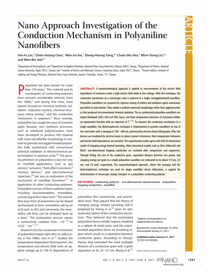
We start to describe and discuss the issue of electrontransport in polyaniline before stepping into experi-mental results. Figure 1a shows a chemical structure ofprotonated (emeraldine salt on the left) and unproto-nated (emeraldine base to the right) polyaniline units.In a first step and starting from a microscopic view-point, it is disclosed30 that an unprotonated polyanilinechain reveals a semiconductor-like band structure witha band gap energy of ∼4 eV. This seems to be inconnection with the Coulomb energy between twonon-overlapping electrons sitting at a distance of thesize of the monomer.18 Since the size of the monomera is ∼0.35 nm, the unscreened Coulomb potential
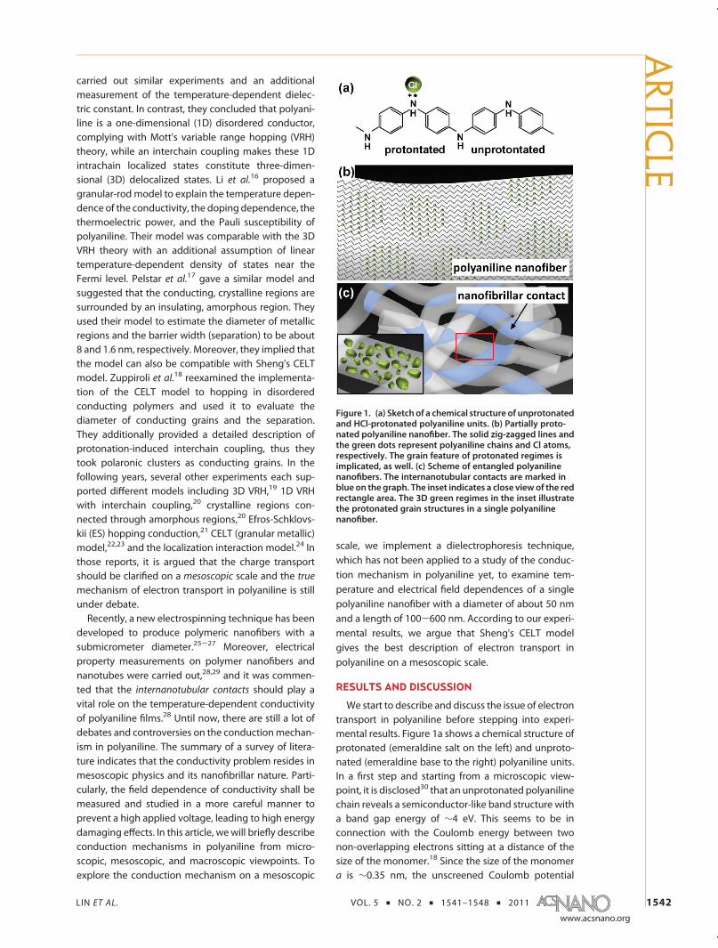
Figure 1. (a) Sketch of a chemical structure of unprotonatedand HCl-protonated polyaniline units. (b) Partially proto-nated polyaniline nanofiber. The solid zig-zagged lines andthe green dots represent polyaniline chains and Cl atoms,respectively. The grain feature of protonated regimes isimplicated, as well. (c) Scheme of entangled polyanilinenanofibers. The internanotubular contacts are marked inblue on the graph. The inset indicates a close view of the redrectangle area. The 3D green regimes in the inset illustratethe protonated grain structures in a single polyanilinenanofiber.
ARTIC
LE
LIN ET AL. VOL. 5 ’ NO. 2 ’ 1541–1548 ’ 2011 1543
www.acsnano.org
energy is simply estimated to be 2 eV by using U = e2/4πε0εra, where e, ε0, and εr = 2 are electron charge,vacuum permittivity, and relative permittivity of poly-aniline, respectively. After being doped by an acid, thepolaron bands form in a protonated chain to demon-strate metallic properties.13,30 The electrical propertiesof most of the polyaniline bulk, however, reveal semi-conducting rather than metallic manners in the tem-perature dependence of resistivity.31 In previousreports,12,17 the model of conducting grains (Figure 1b)in nanofibers has been proposed for either partially orfully protonated polyaniline. The model of partiallyprotonated polyaniline can readily be considered asprotonated regimes, constituting conducting grainsand separated by unprotonated polyaniline. On theother hand, as for the model of the fully protonatedpolyaniline, the amorphous polyaniline, nonstoichio-metry or contacts between nanofibers are regarded asinsulators separating the conducting grains. The Cou-lomb (charging) energy EC between a pair of identicalgrains of diameter d and the intergrain distance s canbe estimated, from the equation18
EC ¼ 2Ua=(d(1þ d=2s)) (1)
to be in the range of a hundred millielectronvolts,which is merely 1/10 of the Coulomb energy of elec-trons sitting at nearest-neighbor benzenes. Figure 1cand its inset present schematically the nanofibrillarnature of polyaniline and the conducting grains in asingle nanofiber. In order to exclude the internano-tubular contact effects, the conduction mechanismon a mesoscopic scale shall be investigated in asingle polyaniline nanofiber. Moreover, instead ofusing fully protonated polyaniline, we implement
partially protonated polyaniline for studies of the con-duction mechanism.Figure 2a shows a typical scanning electron micro-
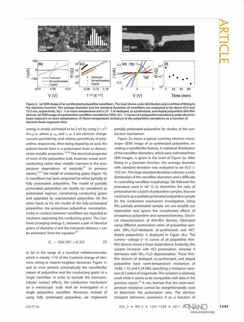
scope (SEM) image of as-synthesized polyaniline, re-vealing a nanofibrillar feature. A statistical distributionof the nanofiber diameters, whichwere estimated fromSEM images, is given in the inset of Figure 2a. Afterfitting to a Gaussian function, the average diameterwith standard deviation was evaluated to be 45.0 (19.3 nm. This large standard deviation indicates a widedistribution of the nanofiber diameters and a difficultyin controlling nanofiber morphology. We followed theprocedure used in ref 12 to determine the ratio ofprotonation for a batch of polyaniline samples, thus wecould pick up a partially protonated polyaniline samplefor the conduction mechanism investigation. Usingthis partially protonated sample, we can simplify ourexploration and ignore the complicated effects ofamorphous polyaniline and nonstoichiometry. Electri-cal characterization of thin-film devices, fabricatedusing different protonation ratios of polyaniline sam-ples (NH3 3H2O-dedoped, as-synthesized, and HCl-doped polyaniline), is displayed in Figure 2b,c. Thecurrent-voltage (I-V) curves of all polyaniline thin-film devices reveal a linear dependence. Evidently, thecurrent increases with HCl protonation, whereas itdecreases with NH3 3H2O deprotonation. These thin-film devices of dedoped, as-synthesized, and dopedpolyaniline have room-temperature resistances of18.80, 1.75, and 0.24 MΩ, specifying a resistance varia-tion of 2 orders ofmagnitude. This variation is relativelysmall while it seems to be compatible with data in theprevious report.12 It was learned that the room-tem-perature resistance cannot be straightforwardly usedto determine the protonation ratio. The electrontransport behaviors (resistance R as a function of
Figure 2. (a) SEM imageof as-synthesized polyaniline nanofibers. The inset shows a size distribution and a red line offitting tothe Gaussian function. The average diameter and the standard deviation of nanofibers are evaluated to be about 45.0 and19.3 nm, respectively. (b) I-V at room temperature and (c) R-T of dedoped, as-synthesized, and doped polyaniline thin-filmdevices. (d) SEM imageof a polyaniline nanofiber nanodevice (S04). (e) I-V curves of a polyaniline nanodevice under electron-beam exposure at room temperature. (f) Room-temperature resistance of the polyaniline nanodevice as a function ofelectron-beam exposure time.
ARTIC
LE
LIN ET AL. VOL. 5 ’ NO. 2 ’ 1541–1548 ’ 2011 1544
www.acsnano.org
temperature T) were in turn measured (Figure 2c) andanalyzed according to the CELT model14
R ¼ R0exp((T0=T)1=p) (2)
where p=2,R0 and T0 are parameters. It is apparent thatall of the three thin-film devices reveal a characteristicR-T behavior in agreement with eq 2. Moreover, theparameter T0 was evaluated to be about 1.9 � 104,8.7 � 103, and 3.3 � 103 K for thin-film devices ofdedoped, as-synthesized, and doped polyaniline. Com-paring the T0 valuewith the data in the inset of Figure 2in ref 12, we determined the protonation ratio of ouras-synthesized polyaniline to be about 57%. The as-synthesized sample is then selected as the partiallyprotonated polyaniline and applied to the investiga-tion of the conduction mechanism.To study electrical properties of a single polyaniline
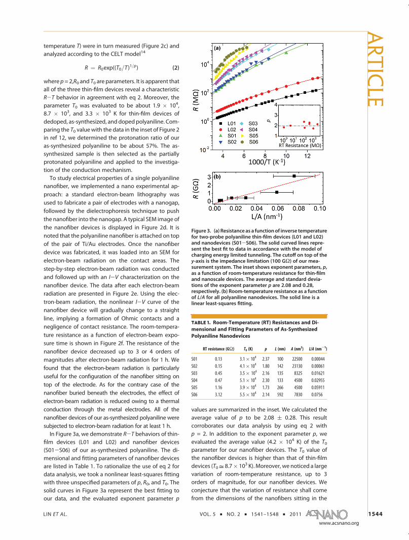
nanofiber, we implemented a nano experimental ap-proach: a standard electron-beam lithography wasused to fabricate a pair of electrodes with a nanogap,followed by the dielectrophoresis technique to pushthe nanofiber into the nanogap. A typical SEM image ofthe nanofiber devices is displayed in Figure 2d. It isnoted that the polyaniline nanofiber is attached on topof the pair of Ti/Au electrodes. Once the nanofiberdevice was fabricated, it was loaded into an SEM forelectron-beam radiation on the contact areas. Thestep-by-step electron-beam radiation was conductedand followed up with an I-V characterization on thenanofiber device. The data after each electron-beamradiation are presented in Figure 2e. Using the elec-tron-beam radiation, the nonlinear I-V curve of thenanofiber device will gradually change to a straightline, implying a formation of Ohmic contacts and anegligence of contact resistance. The room-tempera-ture resistance as a function of electron-beam expo-sure time is shown in Figure 2f. The resistance of thenanofiber device decreased up to 3 or 4 orders ofmagnitudes after electron-beam radiation for 1 h. Wefound that the electron-beam radiation is particularlyuseful for the configuration of the nanofiber sitting ontop of the electrode. As for the contrary case of thenanofiber buried beneath the electrodes, the effect ofelectron-beam radiation is reduced owing to a thermalconduction through the metal electrodes. All of thenanofiber devices of our as-synthesized polyaniline weresubjected to electron-beam radiation for at least 1 h.In Figure 3a, we demonstrate R-T behaviors of thin-
film devices (L01 and L02) and nanofiber devices(S01-S06) of our as-synthesized polyaniline. The di-mensional and fitting parameters of nanofiber devicesare listed in Table 1. To rationalize the use of eq 2 fordata analysis, we took a nonlinear least-squares fittingwith three unspecified parameters of p, R0, and T0. Thesolid curves in Figure 3a represent the best fitting toour data, and the evaluated exponent parameter p
values are summarized in the inset. We calculated theaverage value of p to be 2.08 ( 0.28. This resultcorroborates our data analysis by using eq 2 withp = 2. In addition to the exponent parameter p, weevaluated the average value (4.2 � 104 K) of the T0parameter for our nanofiber devices. The T0 value ofthe nanofiber devices is higher than that of thin-filmdevices (T0= 8.7� 103 K). Moreover, we noticed a largevariation of room-temperature resistance, up to 3orders of magnitude, for our nanofiber devices. Weconjecture that the variation of resistance shall comefrom the dimensions of the nanofibers sitting in the
Figure 3. (a) Resistance as a functionof inverse temperaturefor two-probe polyaniline thin-film devices (L01 and L02)and nanodevices (S01-S06). The solid curved lines repre-sent the best fit to data in accordance with the model ofcharging energy limited tunneling. The cutoff on top of they-axis is the impedance limitation (100 GΩ) of our mea-surement system. The inset shows exponent parameters, p,as a function of room-temperature resistance for thin-filmand nanoscale devices. The average and standard devia-tions of the exponent parameter p are 2.08 and 0.28,respectively. (b) Room-temperature resistance as a functionof L/A for all polyaniline nanodevices. The solid line is alinear least-squares fitting.
TABLE 1. Room-Temperature (RT) Resistances and Di-
mensional and Fitting Parameters of As-Synthesized
Polyaniline Nanodevices
RT resistance (GΩ) T0 (K) p L (nm) A (nm2) L/A (nm-1)
S01 0.13 3.1� 104 2.37 100 22500 0.00044S02 0.15 4.1� 104 1.80 142 23130 0.00061S03 0.45 3.5� 104 2.16 135 8325 0.01621S04 0.47 5.1� 104 2.30 133 4500 0.02955S05 1.16 3.9� 104 1.73 266 4500 0.05911S06 3.12 5.5� 104 2.14 592 7830 0.0756
ARTIC
LE
LIN ET AL. VOL. 5 ’ NO. 2 ’ 1541–1548 ’ 2011 1545
www.acsnano.org
nanogap. The room-temperature resistance is there-fore drawn in Figure 3b as a function of the length L
and the cross-sectional area A of the polyaniline nano-fibers. The room-temperature resistance R is almostlinearly dependent on L/A, suggesting an agreementwith theOhm's lawof R= FL/A, where F is the resistivity.The linear least-squares fitting in Figure 3b was con-ducted to derive a room-temperature resistivity of theas-synthesized polyaniline to be about 103 Ω 3 cm. Thisvalue is about 4 orders of magnitude larger than theresistivity (∼0.1 Ω 3 cm) of fully doped polyaniline, asreported previously.12
In addition to the CELT model, there are two othertheoretical models, the ES hopping conduction and 1DMott's VRH, sharing the same mathematical formula ofeq 2 with p = 2. We examine first the sufficientconditions required to apply the ES hopping conduc-tion to electron transport in a single nanofiber. It wasremarked in the literature that the ES hopping con-duction can only be observed at temperatures lowerthan the critical temperature TC = e4ξg0/kB(4πεrε0)
2,32
where e, ξ, g0, kB, εr, and ε0 are electron charge,localization length, density of states at Fermi level,Boltzmann constant, relative permittivity, and permit-tivity of vacuum, respectively. Above the critical tem-perature, the Coulomb interaction between twolocalized electron states can be neglected and theMott's VRH is valid. The localization length ξ can beevaluated using the parameter T0 and the relation ξ =2.8e2/4πεrε0kBT0.
32 In our nanofiber devices, the para-meter T0 is 4.2 � 104 K and the localization length ξ isabout 0.6 nm. Taking εr = 2 and g0= 1019 eV-1 cm-3 33
into account, the critical temperature TC is estimated tobe about 35 K. This critical temperature is definitelylower than the experimental temperature range, im-plicating that the ES hopping conduction is inade-quately adopted to describe electron transport inpolyaniline nanofibers. We therefore exclude the pos-sibility of considering the ES hopping model as aconduction mechanism in polyaniline nanofibers.The next step is to check that whether 1DMott's VRH
or the CELTmodel is more suitable to describe electrontransport in the polyaniline nanofiber. Both of themodels suggest the same temperature behavior(eq 2 with p = 2) of resistance in the regime of lowelectric field, but different field dependences of resis-tance in high electric fields. In the high-field regime,the differential resistance as a function of electric field Eis expressed as14,20
R ¼ RTexp((E0=E)1=q) (3)
where E0 and q are constant parameters and RT is atemperature-dependent parameter. It is argued thatthe exponent parameter q values are 1 and 2 for theCELT model and 1D Mott's VRH, respectively. In thehigh-field regime, the resistance measurement is moredifficult since a high voltage up to 100 V is required for
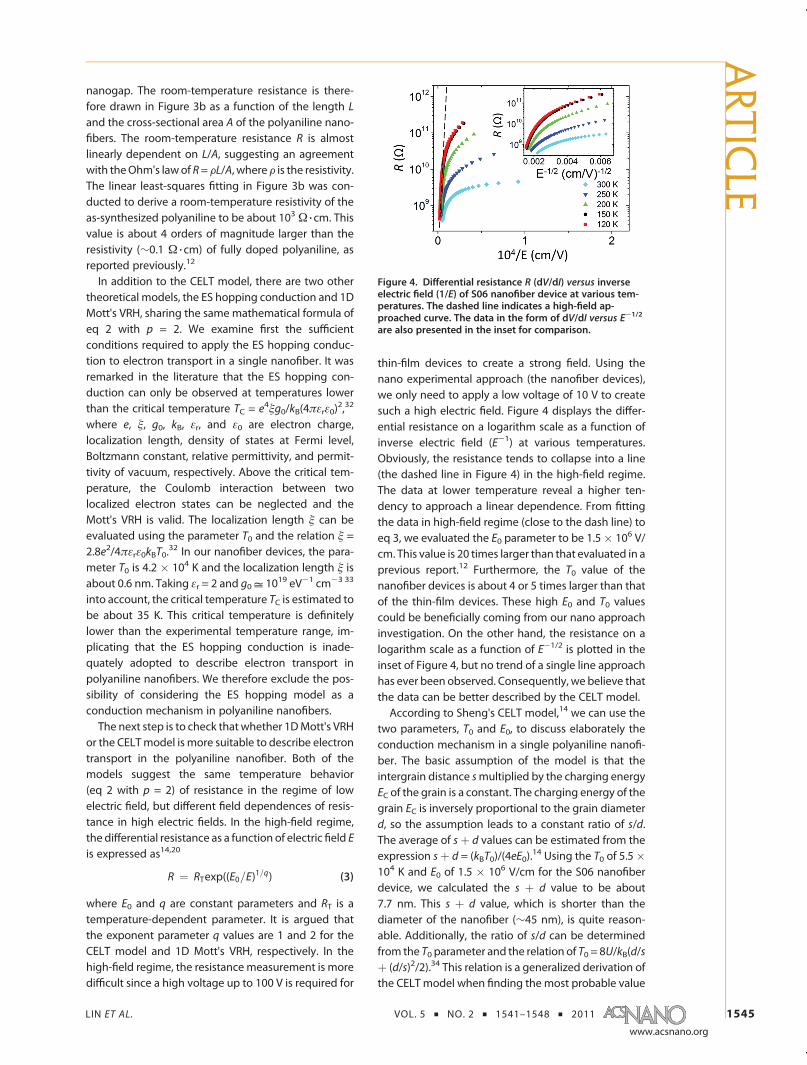
thin-film devices to create a strong field. Using thenano experimental approach (the nanofiber devices),we only need to apply a low voltage of 10 V to createsuch a high electric field. Figure 4 displays the differ-ential resistance on a logarithm scale as a function ofinverse electric field (E-1) at various temperatures.Obviously, the resistance tends to collapse into a line(the dashed line in Figure 4) in the high-field regime.The data at lower temperature reveal a higher ten-dency to approach a linear dependence. From fittingthe data in high-field regime (close to the dash line) toeq 3, we evaluated the E0 parameter to be 1.5� 106 V/cm. This value is 20 times larger than that evaluated in aprevious report.12 Furthermore, the T0 value of thenanofiber devices is about 4 or 5 times larger than thatof the thin-film devices. These high E0 and T0 valuescould be beneficially coming from our nano approachinvestigation. On the other hand, the resistance on alogarithm scale as a function of E-1/2 is plotted in theinset of Figure 4, but no trend of a single line approachhas ever been observed. Consequently, we believe thatthe data can be better described by the CELT model.According to Sheng's CELT model,14 we can use the
two parameters, T0 and E0, to discuss elaborately theconduction mechanism in a single polyaniline nanofi-ber. The basic assumption of the model is that theintergrain distance smultiplied by the charging energyEC of the grain is a constant. The charging energy of thegrain EC is inversely proportional to the grain diameterd, so the assumption leads to a constant ratio of s/d.The average of sþ d values can be estimated from theexpression sþ d = (kBT0)/(4eE0).
14 Using the T0 of 5.5�104 K and E0 of 1.5 � 106 V/cm for the S06 nanofiberdevice, we calculated the s þ d value to be about7.7 nm. This s þ d value, which is shorter than thediameter of the nanofiber (∼45 nm), is quite reason-able. Additionally, the ratio of s/d can be determinedfrom the T0 parameter and the relation of T0 = 8U/kB(d/sþ (d/s)2/2).34 This relation is a generalized derivation ofthe CELT model when finding the most probable value
Figure 4. Differential resistance R (dV/dI) versus inverseelectric field (1/E) of S06 nanofiber device at various tem-peratures. The dashed line indicates a high-field ap-proached curve. The data in the form of dV/dI versus E-1/2
are also presented in the inset for comparison.
ARTIC
LE
LIN ET AL. VOL. 5 ’ NO. 2 ’ 1541–1548 ’ 2011 1546
www.acsnano.org
of the intergrain distance s.18 The s/d ratio is evaluatedto be about 0.6 for the S06 nanofiber device. Thus, theaverage of intergrain distance s and the grain diameterd are about 2.8 and 4.9 nm, respectively. The chargingenergy of the conducting grains can then be estimatedto be ∼78 meV from eq 1. This high charging energy,which is higher than thermal energy at room tempera-ture (25 meV), ascertains that the CELT model can beapplied to the temperature range of our experiment.To understand more about the CELT model, we
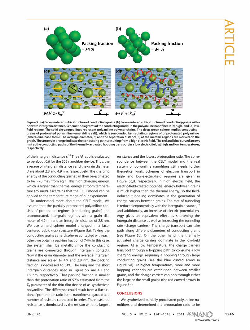
assume that the partially protonated polyaniline con-sists of protonated regimes (conducting grains) andunprotonated, intergrain regimes with a grain dia-meter of 4.9 nm and an intergrain distance of 2.8 nm.We use a hard sphere model arranged in a face-centered cubic (fcc) structure (Figure 5a). Taking theconducting grains as hard spheres contactedwith eachother, we obtain a packing fraction of 74%. In this case,the system shall be metallic since the conductinggrains are connected through intergrain contacts.Now if the grain diameter and the average intergraindistance are scaled to 4.9 and 2.8 nm, the packingfraction is decreased to 34%. The long and the shortintergrain distances, used in Figure 5b, are 4.1 and1.5 nm, respectively. That packing fraction is smallerthan the protonation ratio of 57% estimated from theT0 parameter of the thin-film device of as-synthesizedpolyaniline. The difference could result from a fluctua-tion of protonation ratio in the nanofiber, regarded as anumber of resistors connected in series. The measuredresistance is dominated by the resistor with the largest
resistance and the lowest protonation ratio. The corre-spondence between the CELT model and the realsystem of polyaniline nanofibers still needs furthertheoretical work. Schemes of electron transport inhigh- and low-electric-field regimes are given inFigure 5c,d, respectively. In high electric field, theelectric-field-created potential energy between grainsis much higher than the thermal energy, so the field-induced tunneling dominates in the generation ofcharge carriers between grains. The rate of tunnelingis reduced exponentially with the intergrain distance,14
and additionally, an increase of electric potential en-ergy gives an equivalent effect as shortening theintergrain distance as well as increasing the tunnelingrate (charge carriers). The charge transport can takepath along different diameters of conducting grains(see Figure 5c). On the other hand, the thermallyactivated charge carriers dominate in the low-fieldregime. At a low temperature, the charge carrierstransport through a hopping path to consume a lowcharging energy, requiring a hopping through largeconducting grains (see the blue curved arrow inFigure 5d). At higher temperatures, more and morehopping channels are established between smallergrains, and the charge carriers can hop through eitherthe large or the small grains (the red curved arrows inFigure 5d).
CONCLUSIONS
We synthesized partially protonated polyaniline na-nofibers and determined the protonation ratio to be
Figure 5. (a) Face-centered cubic structure of conducting grains. (b) Face-centered cubic structure of conductinggrainswith anonzero intergrain distance. Schematic diagramsof the conductingmodel in thepolyanilinenanofiber in (c) high- and (d) low-field regime. The solid zig-zagged lines represent polyaniline polymer chains. The deep green sphere implies conductinggrains of protonated polyaniline (emeraldine salt), which is surrounded by insulating regions of unprotonated polyaniline(emeraldine base form). The average diameter, d, and the separation distance, s, of the metallic regions are marked on thegraph. The arrows in orange indicate the conducting paths resulting from a high electric field. The red and blue curved arrowshint at the conducting paths of the thermally activated hopping transport in a low electric field at high and low temperatures,respectively.
ARTIC
LE
LIN ET AL. VOL. 5 ’ NO. 2 ’ 1541–1548 ’ 2011 1547
www.acsnano.org
57% by analyzing the temperature-dependent resis-tance of thin-film devices. Techniques of electron-beam lithography and dielectrophoresis are imple-mented to fabricate nanofiber devices of the as-synthesized polyaniline. Through data analysis, weargued that the conduction mechanism is best de-scribed by the CELT model, rather than the ES hoppingor the 1D Mott's VRH model. Using the CELT model toanalyze temperature- and electric-field-dependent re-sistances of nanofiber devices, we estimated the valuesof T0 and E0 parameters to be larger than thosecalculated from data of thin-film devices. The T0 andE0 parameters are applied to determine the conductinggrain diameter (∼4.9 nm) and the intergrain distance
(∼2.8 nm) in a single nanofiber. According to the CELTmodel, electron transport in a single polyaniline nano-fiber is expressed schematically in detail. In a highelectric field, the electric-field-induced tunneling dom-inates charge transport. In a low electric field, thethermal-energy-activated tunneling is in competitionwith the Coulomb charging energy of the conductinggrains. Thus the carriers take the hopping path throughlarge conducting grains at low temperatures, andmoreand more hopping paths connecting small grains areestablished with increasing temperature. The true con-duction mechanism on a mesoscopic scale is exploredand elucidated in a single polyaniline nanofiberthrough the nano experimental approach.
METHODS
Synthesis. Polyaniline nanofibers were synthesized by using arapidly mixed reaction.35 A description of the synthesis methodis given as follows. A solution of ammonium persulfate (0.183 g,0.8 mmol, >99%, Sigma-Aldrich Ltd.) dissolved in 10 mL of 1 MHCl was carefully poured in a solution of aniline (0.298 g, 3.2mmol, >99%, Sigma-Aldrich Ltd.) dissolved in 10 mL of 1 M HCl.The mixed solution was stirred immediately at room tempera-ture. The polymerization began, and the mixed solution hadturned a deep green color. This solution was stirred continu-ously for 24 h. To store polymer solution, 0.5 mLof this solution was fetched and diluted with distilled waterof 10 mL. Polyaniline nanofibers were stocked in the watersolution.
Microscopy. Sampleswere prepared bydropping the polyani-line solution on Si wafers, having a dimension of 7� 7mm2, andtheywere dried beforemicroscopymeasurements. The sampleswere loaded in a high vacuum chamber of a field-emissionscanning electron microscope (JEOL JSM-7000F). Dimensionsand morphology of polyaniline nanofibers were all recordedusing FE-SEM.
Thin-Film Devices. By means of a standard photolithographytechnique, micrometer-scale Ti/Au (∼10/60 nm in thickness)electrodes were deposited on Si wafers capped with a 400 nmthick SiO2 layer to prevent any possible current leakage throughthe substrate. The separation distance between two nearest-neighbor electrodes was about 40 μm. The as-synthesizedpolyaniline solution was either protonated or deprotonatedby washing with 0.25 M HCl or 0.2 M NH3 3H2O solution, res-pectively. Thin-film devices were prepared by dropping thesepolyaniline solutions on the photolithographically prepat-terned Si wafer and dried for hours at room temperature in air.
Nanofiber Devices. In connection with prepatterned micro-meter-scale electrodes on Si wafers, a standard electron-beamlithography technique was used to deposit two submicrometerTi/Au (∼20/100 nm thickness) current leads and to leave a gapof 100-600 nm in width. The resistance between the twocurrent leads and across the empty gap was determined to bemuch higher than 1 TΩ in a bias voltage of (10 V, implying anegligible, low leakage current at room temperature. This highempty-gap resistance guarantees a real measurement of elec-trical properties if the current, flowing through the as-depos-ited, crossing-gap material, is much higher than the leakagecurrent. Here the dielectrophoresis technique was applied toposition polyaniline nanofibers into the gap. To fabricate nano-fiber devices, several drops of polyaniline solutions were put onthe empty-gap device and an alternative current (AC) voltage of1 MHz sinusoidal wave was imposed between two submicrom-eter current leads for 3 min. Thus polyaniline nanofibers wereattracted and positioned into the gap. It is noted that, depend-ing on the width of the gap, the AC driving voltage was varied
between 3 and 6 V. Moreover, a capacitor of 10 μF was seriouslyconnected during the dielectrophoresis process in preventionof any direct-current-induced electrochemical reactions. Afterthe dielectrophoresis process, excess polyaniline solution wasgently blown off the nanofiber device by using nitrogen gas. Inorder to improve electrical contacts between polyaniline nano-fibers and submicrometer leads, the contact pads of thenanofiber devices were exposed to the electron beam of FE-SEM with a dose of 3 � 104 C/m2
3 s for at least 1 h.Electrical Property. Either thin-film or nanofiber two-probe
devices were loaded in a cryostat (variable temperature insertcryostat, CRYO Industries of America Inc.) in helium gas (99.99%)at 760 Torr for acquisition of temperature-dependent electricalbehaviors from 300 to 80 K. The current-voltage measure-ments were carried out by using either Keithley K-6430 or ahomemade system. The homemade electrometer demon-strates a current and voltage resolution of 10 pA and 1 mV,respectively. The impedance limitation of our system, includingthe cryostat and the electrometer, is about 100 GΩ. Theresistance was estimated around the zero bias voltage fromthe current-voltage curves, and its standard deviation wasevaluated to be less than 0.1%.
Acknowledgment. This work was supported by the TaiwanNational Science Council under Grant Numbers NSC 98-2112-M-009-013-MY2 and NSC 98-2923-M-009-001-MY2, and by theMOE ATU Program. W.B.J. thanks P. Sheng (The Hong KongUniversity of Science and Technology) for helpful discussions.
REFERENCES AND NOTES1. Genies, E. M.; Boyle, A.; Lapkowski, M.; Tsintavis, C. Poly-
aninline;A Historical Survey. Synth. Met. 1990, 36, 139–182.
2. Huang, W. S.; Humphrey, B. D.; MacDiarmid, A. G. Polyani-line, a Novel Conducting Polymer. J. Chem. Soc., FaradayTrans. 1 1986, 82, 2385–2400.
3. Jozefowicz, M. E.; Laversanne, R.; Javadi, H. H. S.; Epstein,A. J.; Pouget, J. P.; Tang, X.; MacDiarmid, A. G. MultipleLattice Phases and Polaron-Lattice-Spinless-Defect Com-petition in Polyaniline. Phys. Rev. B1989, 39, 12958–12961.
4. Chiang, C. K.; Fincher, C. R.; Park, Y. W.; Heeger, A. J.;Shirakawa, H.; Louis, E. J.; Gau, S. C.; MacDiarmid, A. G.Electrical Conductivity in Doped Polyacetylene. Phys. Rev.Lett. 1977, 39, 1098–1101.
5. Surwade, S. P.; Manohar, N.; Manohar, S. K. Origin of BulkNanoscale Morphology in Conducting Polymers. Macro-molecules 2009, 42, 1792–1795.
6. Huang, J.; Virji, S.; Weiller, B. H.; Kaner, R. B. NanostructuredPolyaniline Sensors. Chem.;Eur. J. 2004, 10, 1314–1319.
ARTIC
LE
LIN ET AL. VOL. 5 ’ NO. 2 ’ 1541–1548 ’ 2011 1548
www.acsnano.org
7. Baker, C. O.; Shedd, B.; Innis, P. C.; Whitten, P. G.; Spinks,G. M.; Wallace, G. G.; Kaner, R. B. Monolithic Actuators fromFlash-Welded Polyaniline Nanofibers. Adv. Mater. 2008,20, 155–158.
8. Kim, B. K.; Kim, Y. H.; Won, K.; Chang, H.; Choi, Y.; Kong, K. J.;Rhyu, B. W.; Kim, J. J.; Lee, J. O. Electrical Properties ofPolyaniline Nanofiber Synthesized with Biocatalyst. Nano-technology 2005, 16, 1177–1181.
9. Tseng, R. J.; Huang, J; Ouyang, J.; Kanner, R. B.; Yang, Y.Polyaniline Nanofiber/Gold Nanoparticle NonvolatileMemory. Nano Lett. 2005, 5, 1077–1080.
10. B�elanger, D.; Ren, X.; Davey, J.; Uribe, F.; Gottesfeld, S.Characterization and Long-Term Performance of Polyani-line-Based Electrochemical Capacitors. J. Electrochem. Soc.2000, 147, 2923–2929.
11. Tran, H. D; Wang, Y.; D'Arcy, J. M.; Kanner, R. B. Toward anUnderstanding of the Formation of Conducting PolymerNanofibers. ACS Nano 2009, 2, 1841–1848.
12. Zuo, F.; Angelopoulos, M.; MacDiarmid, A. G. TransportStudies of Protonated Emeraldine Polymer: A GranularPolymericMetal System. Phys. Rev. B1987, 36, 3475–3478.
13. Stafstrom, S.; Bredas, J. L.; Epstein, A. J.; Woo, H. S.; Tanner,D. B.; Huang, W. S.; MacDiarmid, A. G. Polaron Lattice inHighly Conducting Polyaniline: Theoretical and OpticalStudies. Phys. Rev. Lett. 1987, 59, 1464–1467.
14. Sheng, P.; Abeles, B.; Arie, Y. Hopping Conductivity inGranular Metals. Phys. Rev. Lett. 1973, 31, 44–47.
15. Wang, Z. H.; Li, C.; Scherr, E. M.; MacDiarmid, A. G.; Epstein,A. J. Three Dimensionality of “Metallic” States in Conduct-ing Polymer: Polyaniline. Phys. Rev. Lett. 1991, 66, 1745–1748.
16. Li, Q.; Cruz, L.; Philips, P. Granular-RodModel for ElectronicConduction in Polyaniline. Phys. Rev. B 1993, 47, 1840–1845.
17. Pelster, R.; Nimtz, G.; Wessling, B. Fully Protonated Polyani-line: Hopping Transport on a Mesoscopic Scale. Phys. Rev.B 1994, 49, 12718–12723.
18. Zuppiroli, L.; Bussac, M. N.; Paschen, S.; Chauvet, O.; Forro,L. Hopping in Disordered Conducting Polymers. Phys. Rev.B 1994, 50, 5196–5203.
19. Li, W.; Wan, M. Porous Polyaniline Films with High Con-ductivity. Synth. Met. 1998, 92, 121–126.
20. Joo, J.; Long, S. M.; Pouget, J. P.; Oh, E. J.; MacDiarmid, A. G.;Epstein, A. J. Charge Transport of the Mesoscopic MetallicState in Partially Crystalline Polyanilines. Phys. Rev. B1998, 57, 9567–9580.
21. Ghosh, M.; Barman, A.; De, S. K.; Chatterjee, S. Crossoverfrom Mott to Efros-Schklovskii Variable-Range-HoppingConductivity in Conducting Polaniline. Synth. Met. 1998,97, 23–29.
22. Plan�es, J.; Wolter, A.; Cheguettine, Y.; Pro�n, A.; Genoud, F.;Nechtschein, M. Transport Properties of Polyaniline-Cellulose-Acetate Blends. Phys. Rev. B 1998, 58, 7774–7785.
23. Chaudhuri, D.; Kumar, A.; Nirmala, R.; Sarma, D. D.; García-Hern�andez, M.; Sharath, L. S.; Ganesan, V. Transport andMagnetic Properties of Conducting Polyaniline Dopedwith BX3 (X = F, Cl, and Br). Phys. Rev. B 2006, 73, 075205.
24. Tzamalis, G.; Zaidi, N. A.; Monkman, A. P. Applicability ofthe Localization-Interaction Model to Magnetoconductiv-ity Studies of Polyaniline Films at the Metal-InsulatorBoundary. Phys. Rev. B 2003, 68, 245106.
25. Li, D.; Wang, Y.; Xia, Y. Electrospining of Polymeric andCeramic Nanofibers as Uniaxially Alligned Arrays. NanoLett. 2003, 3, 1167–1171.
26. Kameoka, J.; Orth, R.; Yang, Y.; Czaplewski, D.; Mathers, R.;Coates, G. W.; Craighead, H. G. A Scanning Tip Electro-spinning Source for Deposition of Oriented Nanofibres.Nanotechnology 2003, 14, 1124–1129.
27. Pinto, N. J.; Johnson, A. T., Jr.; MacDiarmid, A. G.; Mueller,C. H.; Theofylaktos, N.; Robinson, D. C.; Miranda, F. A.Electrospun Polyaniline/Polyethylene Oxide NanofiberField-Effect Transistor. Appl. Phys. Lett. 2003, 83, 4244–4246.
28. Long, Y.; Chen, Z.; Wang, N.; Ma, Y.; Zhang, Z.; Zhang, L.;Wan, M. Electrical Conductivity of a Single Conducting
Polyaniline Nanotube. Appl. Phys. Lett. 2003, 83, 1863–1865.
29. Aleshin, A. N. Polymer Nanofibers and Nanotubes: ChargeTransport and Device Applications. Adv. Mater. 2006, 18,17–27.
30. Varela-�Alvarez, A.; Sordo, J. A. A Suitable Model forEmeraldine Salt. J. Chem. Phys. 2008, 128, 174706.
31. Lee, K.; Cho, S.; Park, S. H.; Heeger, A. J.; Lee, C. W.; Lee, S. H.Metallic Transport in Polyanilline. Nature 2006, 441, 65–68.
32. Efros, A. L.; Shklovskii, B. I. Coulomb Gap and Low Tem-perature Conductivity of Disordered Systems. J. Phys. C:Solid State Phys. 1975, 8, L49–L51.
33. Ghosh, M.; Barman, A.; De, S. K.; Chatterjee, S. TransportProperties of HCl Doped Polyaniline and Polyaniline-Methylcellulose Dispersion. J. Appl. Phys. 1998, 84, 806–811.
34. Wolter, A.; Rannou, P.; Travers, J. P. Model for Aging in HCl-Protonated Polyaniline: Structure, Conductivity, and Com-position Studies. Phys. Rev. B 1998, 58, 7637–7647.
35. Huang, J.; Kaner, R. B. Nanofiber Formation in the Chemi-cal Polymerization of Aniline: AMechanistic Study.Angew.Chem., Int. Ed. 2004, 116, 5941–5945.
ARTIC
LE