nano-imprinting lithography technology - nano...
TRANSCRIPT
Micro/Nano fabrication process 2009-02
Nano-imprinting LithographyTechnology
Nano-fabrication & Micro-Optics LaboratoryYonsei University

Micro/Nano fabrication process 2009-02
Limitation of photolithograph
Agenda
- Remind of photolithography technology
- What is diffraction
- Diffraction limit
Concept of nano-imprinting lithography
Basic process of nano-imprinting lithography technology
Nano-fabrication & Micro-Optics LaboratoryYonsei University

Micro/Nano fabrication process 2009-02
Photoresist process for lithography
Clean substrate
Remind of photolithography technology
Development
Post Baking
Etching
Remove PR
Soft Baking
PR Spin Coating
UV Exposure
Apply Adhesion Promoter(HMDS)
Limitation of photolithography
Nano-fabrication & Micro-Optics LaboratoryYonsei University

Micro/Nano fabrication process 2009-02
UV Exposure
UV Exposure
Real case of photolithography(ultra small pattern size)
Mask
Ideal case of photolithography
Diffraction effect
회절로인해같은조건의촬영시위와같은상이한결과를초래
(Image blur 현상발생)
Photolithography process and limitation
Nano-fabrication & Micro-Optics LaboratoryYonsei University

Micro/Nano fabrication process 2009-02
What is diffraction ?
Basic assumption : Light is wave
Diffraction is the process by which light waves traveling through a small hole, slit or around a boundary will spread out
Nano-fabrication & Micro-Optics LaboratoryYonsei University

Micro/Nano fabrication process 2009-02
What is diffraction ?
Diffraction causes the loss of resolving power
Image blur 현상은각종수차에의해영향을받지만공기중의 particle에의한 diffraction으로인해같은조건의촬영시위와같은상이한결과를초래한다
Nano-fabrication & Micro-Optics LaboratoryYonsei University

Micro/Nano fabrication process 2009-02
Diffraction limit
Example – Diffraction of circular aperture
is a Bessel function of the first kind
Nano-fabrication & Micro-Optics LaboratoryYonsei University

Micro/Nano fabrication process 2009-02
Diffraction limit
D θ
The radius of the Airy disk
Nano-fabrication & Micro-Optics LaboratoryYonsei University

Micro/Nano fabrication process 2009-02
Imprinting Technology
Nano-fabrication & Micro-Optics LaboratoryYonsei University

Micro/Nano fabrication process 2009-02
<금속활자본>
현존하는가장오래된금속활자본직지심체요절
• 정식명칭: 백운화상초록불조직지심체요절
• 1377년(고려우왕 3) 7월청주흥덕사간행
• 세계에서가장 오래된금속활자본
• 1372년쓰여진책을 77년금속, 78년목판으로간행
• 금속활자본은현재 프랑스국립도서관에소장
• 2001년유네스코세계기록유산등재
<목판본>
<금속활자본표지>
Imprinting
자료출처: http://www.jikjiworld.netNano-fabrication & Micro-Optics LaboratoryYonsei University

Micro/Nano fabrication process 2009-02
직지심체요절금속활자제작및 인쇄과정
< 글자본선정> < 자본붙이기> < 어미자만들기> < 주형틀만들기>
< 쇳물붓기> < 활자떼어내기> < 조판> < 인쇄>
Imprinting
자료출처: http://www.jikjiworld.netNano-fabrication & Micro-Optics LaboratoryYonsei University

Micro/Nano fabrication process 2009-02
2. Press mold
3. Remove mold
1. Mold fabricaion step- Using E-beam lithography, FIB, etc.
2. Imprinting step- Nano mold with nano-scale pattern
is pressed into a resist
Mold
ResistSubstrate
Mold
ResistSubstrate
Mold
1. Mold fabrication
< Mold >
< Resist pattern >
Nano-imprinting process
Nano-fabrication & Micro-Optics LaboratoryYonsei University

Micro/Nano fabrication process 2009-02
Nano-imprinting 기술의종류
Nano-fabrication & Micro-Optics LaboratoryYonsei University

Micro/Nano fabrication process 2009-02
Basic process of nano-imprinting lithography technology
Procedure of nanoimprinting lithography : 2 basic step
1. Pressing mold
2. Remove mold
3. Pattern transfer (RIE)
resistsubstrate
resistmold
resistsubstrate
resistmold
resistsubstrate
1. Imprint step- Nano mold with nano-scale pattern
is pressed into a resist
2. Pattern transfer step- Pattern transfer to substrate by RIE
(Reactive Ion Etching)
- RIE is used to remove the residual resist in the compressed area
Ref) Proc. SPIE 4349, (2001), p. 82
< Mold >
< Resist pattern >
Nano-fabrication & Micro-Optics LaboratoryYonsei University

Micro/Nano fabrication process 2009-02
Heating of Substrate and Mold
to above Tg
Application ofMolding Pressure
Cooling of Substrate and Mold
to below Tg
Demolding
Procedures
1. Press mold with heat
2. Remove mold
Mold
ResistSubstrate
Mold
ResistSubstrate
< Mold >
< Imprinted resist >
Thermal nano-imprinting lithography technology
Ref) http://www.obducat.com/Default.aspx?ID=187Nano-fabrication & Micro-Optics LaboratoryYonsei University

Micro/Nano fabrication process 2009-02
UV nano-imprinting• Material: UV-curable photopolymer• Processing condition: room temp. & low pressure• No fluidity problem
Procedures <Pyramid pattern><Lattice pattern>
Photopolymer dispensationon substrate
Covering the mold Aligning
Releasing the mold
PhotopolymerSubstrate
UV-transparent mold
UV-light
Pressure
UV nano-imprinting lithography technology
Ref) http://www.obducat.com/Default.aspx?ID=187 JJAP, vol. 44, No. 7B, pp. 5600, 2005Nano-fabrication & Micro-Optics LaboratoryYonsei University

Micro/Nano fabrication process 2009-02
Design and construction of continuous UV nano imprinting system
For flexible substrate
For rigid substrate
1. Can replicate nano patterns of large area with high precision
2. Can replace conventional lithography process
Fabrication results
Continuous UV nano-imprinting lithography technology
Nano-fabrication & Micro-Optics LaboratoryYonsei University

Micro/Nano fabrication process 2009-02
Ref) Resin micromachining by roller hot embossing, microsystem technology, 2007Ref) Subdivision Surfaces for procedural Design of Imprint Rolls, SPM, 2008
Schematic diagram of the mold fabrication process performed in Ref Paper
Roll NIL -Roll mold-
Nano-fabrication & Micro-Optics LaboratoryYonsei University

Micro/Nano fabrication process 2009-02
Ref) Large-Area Roll-to-Roll and Roll-to-Plate Nanoimprint Lithography: A Step towardHigh-Throughput Application of Continuous Nanoimprinting, 2008, ACSNANORef) Rigiflex Lithography nanostructure transfer, Advanced Material, 2005
Nano-fabrication & Micro-Optics LaboratoryYonsei University
Roll NIL -Flexible mold-
Micro/Nano fabrication process 2009-02
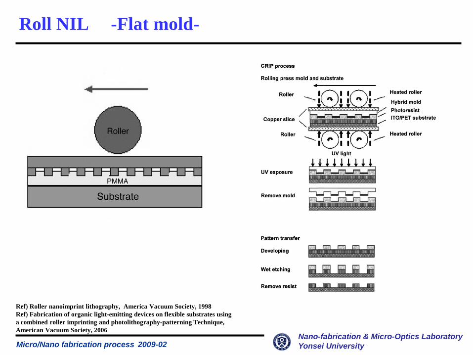
Ref) Roller nanoimprint lithography, America Vacuum Society, 1998Ref) Fabrication of organic light-emitting devices on flexible substrates usinga combined roller imprinting and photolithography-patterning Technique, American Vacuum Society, 2006
Nano-fabrication & Micro-Optics LaboratoryYonsei University
Roll NIL -Flat mold-

Micro/Nano fabrication process 2009-02
Roll to Roll Imprinting Technology
Nano-fabrication & Micro-Optics LaboratoryYonsei University

Micro/Nano fabrication process 2009-02
Roll-to-roll processing, also known as 'web' processing, reel-to-reel processing or R2R, is the process of creating electronic devices on a roll of flexible plastic or metal foil.Large circuits made with thin-film transistors and other devices can be easily patterned onto these large substrates, which can be up to a few metres wide and 50 km long.Roll-to-roll processing is a technology which is still in development. If semiconductor devices can be fabricated in this way on large substrates, many devices could be fabricated at a fraction of the cost of traditional semiconductor manufacturing methods. Applications could arise which take advantage of the flexible nature of the substrates, such as electronics embedded into clothing, large-area flexible displays, and roll-up portable displays.
Ref) http://www.gizmag.com/tag/oled/2/http://en.wikipedia.org/wiki/Roll-to-roll_processinghttp://www.geeky-gadgets.com/hp-develops-a-flexible-plastic-display/
<R2R Process for OLED(GE)> <R2R Process for Flexible display(HP)>
1. Introduction : Roll to roll process
Nano-fabrication & Micro-Optics LaboratoryYonsei University

Micro/Nano fabrication process 2009-02
Metal 증착 방법 - 진공공정
<Method 1> <Method 2>
P PP
2. Roll to roll micro lithography
Nano-fabrication & Micro-Optics LaboratoryYonsei University
AUnexposed polymer Removing
B Rinse
C Drying
D Metal etching
E Polymer Removing
Metal coated film feeding
Polymer Coating
UnexposedPhotopolymer removing
UV rollImprintingLithography
MetalEtching
Polymer Removing
Final patterns
System formation

Micro/Nano fabrication process 2009-02
3. Roll to roll micro printing
Nano-fabrication & Micro-Optics LaboratoryYonsei University
Ref) www.moazine.com

Micro/Nano fabrication process 2009-02Nano-fabrication & Micro-Optics LaboratoryYonsei University
Ref) www.nanoprinttech.com
3. Roll to roll micro printing : electronics printing

Micro/Nano fabrication process 2009-02Nano-fabrication & Micro-Optics LaboratoryYonsei University
Ref) www.kosen21.org
3. Roll to roll micro printing : printing

Micro/Nano fabrication process 2009-02
… printing is a micro structuring technique ! but since hundreds of years, 99% of all printing applications are for visual usage, not for electronic functions.
Printing is expanded all manufacture process
Nano-fabrication & Micro-Optics LaboratoryYonsei University
Ref) www.electronics.ca
3. Roll to roll micro printing : limit of printing process
Micro/Nano fabrication process 2009-02Nano-fabrication & Micro-Optics LaboratoryYonsei University
Ref) www.idtechex.com
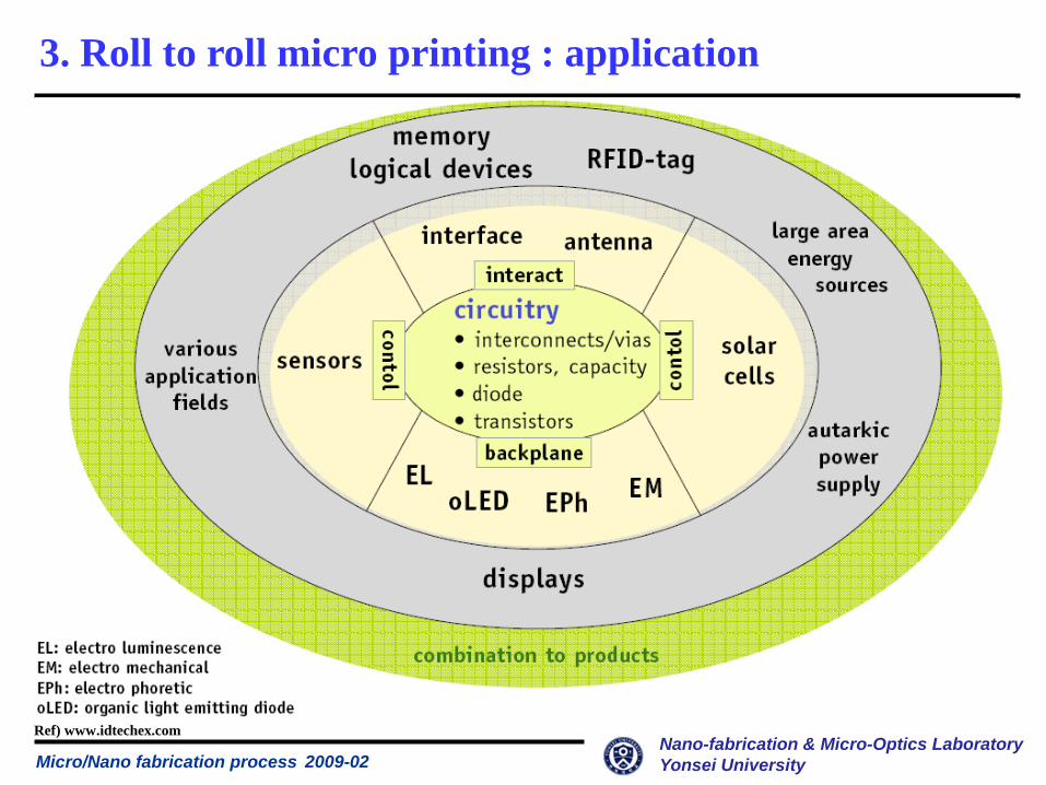
3. Roll to roll micro printing : application

Micro/Nano fabrication process 2009-02
Good for flexible substrates, bad for glassWell suited for solvent-based organic semiconductors and thin filmsHigh throughputDemonstrated Flex OLED and TFT: DNP, Add-Vision, VTT, Berkeley
Line resolution > 50umHigh pattern setup costs
Cylinder pattern
Gravure is an intaglio printing process.The image carrier has the image cut or etched below the surface of the non-image area.On the gravure image carrier (usually a copper cylinder), all the images are screened,creating thousands of tiny cells.During printing, the image carrier is immersed in fluid ink. As the image carrier rotates,ink fills the tiny cells and covers the surface of the cylinder. The surface of the cylinder iswiped with a doctor blade, leaving the non-image area clean while the ink remains in therecessed cells.
Source: www.gaa.org
What is Gravure?
Summary of technology
Concerns
Nano-fabrication & Micro-Optics LaboratoryYonsei University
3. Roll to roll micro printing : gravure printing

Micro/Nano fabrication process 2009-02
Definition: With gravure printing an image is etched on the surface of a metal plate, the etched area is filled with ink, then the plate is rotated on a cylinder that transfers the image to the paper or other material
Ref) www.schur.com& International paper knowledge center
• High quality and expensive• Used for high quality photographic images • Opposite of relief printing plate created with engraved image creating cells of ink color• Ink is spirit based and dries immediately• Gravure printing is often used for high-volume printing of packaging, wallpaper, and gift wrap.
Although less common, gravure printing may also be used for printing magazines, greeting cards, and high-volume advertising.
Gravure printingNano-fabrication & Micro-Optics LaboratoryYonsei University
3. Roll to roll micro printing : gravure printing

Micro/Nano fabrication process 2009-02
Sheet-fed
Wed-fed
Concept of offset printing
Nano-fabrication & Micro-Optics LaboratoryYonsei University
Press Types: sheet-fed and web-fed
3. Roll to roll micro printing : gravure printing

Micro/Nano fabrication process 2009-02
Blanket, ink paste, transferDemonstrated 20 ~ 30μm line widthAccuracy: 2.5μm / 400mm,Repeatability: <2.5 μm
Line resolution > 50umHigh pattern setup costs
Ref) Stanford University
Feeding system: The feeding system is the device that feeds the paper into the press.Printing system: The printing system for offset presses contain 3 major components: the plate cylinder, blanket cylinder, and the impression cylinderInking system:The inking system on offset presses consists of a fountain which holds the ink and a set of rollers, known as the roller train, which distribute the ink and carry it to the printing plate.Dampening system:Delivery system:
Nano-fabrication & Micro-Optics LaboratoryYonsei University
Press components
Summary of technology
Concerns
3. Roll to roll micro printing : gravure printing

Micro/Nano fabrication process 2009-02
Gravure-offset printing
In gravure-offset printing, the ink (or paste) is first doctored into the grooves of a gravures plate. An offset pad or-roller, made of a rubber or silicone polymer, picks up the ink from the gravure grooves by pressing against it. Then the pad or roller transfers the ink to the substrate by pressing or rotating over it. After that, the conductor inks for ceramics are dried and fired at 600–900 C.
Printed substrate (below) and ink left on blanket (above)Flow of roller type gravure offset printing.
Nano-fabrication & Micro-Optics LaboratoryYonsei University
Ref) Marko Pudas, Juha Hagberg, Seppo Leppa¨ vuori, ”Printing parameters and ink components affecting ultra-fine-line gravure-offset printing for electronics applications” Journal of the European Ceramic Society 24 (2004) 2943–2950
3. Roll to roll micro printing : gravure-offset printing

Micro/Nano fabrication process 2009-02
Gravure-offset printing
300 and 20 um wide dried lines 37.5 and 50 um wide dried lines printed with ink
50 mm wide Au conductors on a PZT layer in a pressure sensor structure.
100 mm wide Ag conductors printed over a 90o
corner of a ceramic substrate.
Nano-fabrication & Micro-Optics LaboratoryYonsei University
Ref) M. Lahti , S. Leppa¨vuori, V. Lantto, ”Gravure-offset-printing technique for the fabrication of solid films” Applied Surface Science 142 1999. 367–370
3. Roll to roll micro printing : gravure-offset printing

Micro/Nano fabrication process 2009-02
• Non contact – Low impact to object
• Low cost – Lithography and developing process unneeded
• Scalability – It can be set up to produce very small quantities and size to very large quantities and size
• Efficient material use– Ink jet is direct write, effectively no waste
Ink jettechnology
Drop-on-Demand
Thermal Piezoelectric
Continuous
4. Roll to roll ink-jet printing technology
Nano-fabrication & Micro-Optics LaboratoryYonsei University
Why ink-jet?

Micro/Nano fabrication process 2009-02
Thermal ink jet process
Piezoelectric ink jet process
Nano-fabrication & Micro-Optics LaboratoryYonsei University
Continuous ink-jet
Drop on demand ink-jet
4. Roll to roll ink-jet printing technology

Micro/Nano fabrication process 2009-02Nano-fabrication & Micro-Optics LaboratoryYonsei University
4. Roll to roll ink-jet printing technology : application

Micro/Nano fabrication process 2009-02
Imprinting system
Nano-fabrication & Micro-Optics LaboratoryYonsei University

Micro/Nano fabrication process 2009-02
■ History
• 1980 – Foundation of Electronic Visions• 1985 – Creation of the world’s first double-side mask aligner• 1992 – Development of the first performance wafer bonding systems• 1997 – Entered the nanotechnology market with the development of the first nanoimprinting system• 1998 – Development of the revolutionary cavity coating technology
• 2000 – Introduction of Fully-automated and integrated production systems • 2001 – Design & Installation of the first 300mm automated SOI production bonder• 2006 – Release of bond cluster module for SOI market• 2008 – Release of production wafer bonder for 3D applications
EVG
Ref) www.gvgroup.comNano-fabrication & Micro-Optics LaboratoryYonsei University

Micro/Nano fabrication process 2009-02
■ Products
• Lithography – Mask aligner SystemsResist Processing SystemsLithography Track SystemsNanoimprint Lithography Systems (UV-NIL, μCP, HE)Inspection Systems
• Bonding – Wafer Bonding SystemsBond Alignment SystemsIntegrated Bonding SystemsSOI Bonding Systems Temporary Bonding and Debonding SystemsInspection Systems
EVG
Ref) www.gvgroup.comNano-fabrication & Micro-Optics LaboratoryYonsei University

Micro/Nano fabrication process 2009-02
■ EVG 620 Bond Aligner
• Features
- bond alignment of 2~3 wafer stacks up 150nm wafer sizes
- Manual or motorized alignment stage
- Fully motorized high resolution bottom side microscopes
- Quick tool change between different wafer sizes and bonding
- Easy to use Windows based operation
• Technical Data
- Alignment methods
>Backside alignment : ± 2μm >Transparent alignment : ± 1μm >IR alignment : option
EVG
Ref) www.gvgroup.comNano-fabrication & Micro-Optics LaboratoryYonsei University
Micro/Nano fabrication process 2009-02
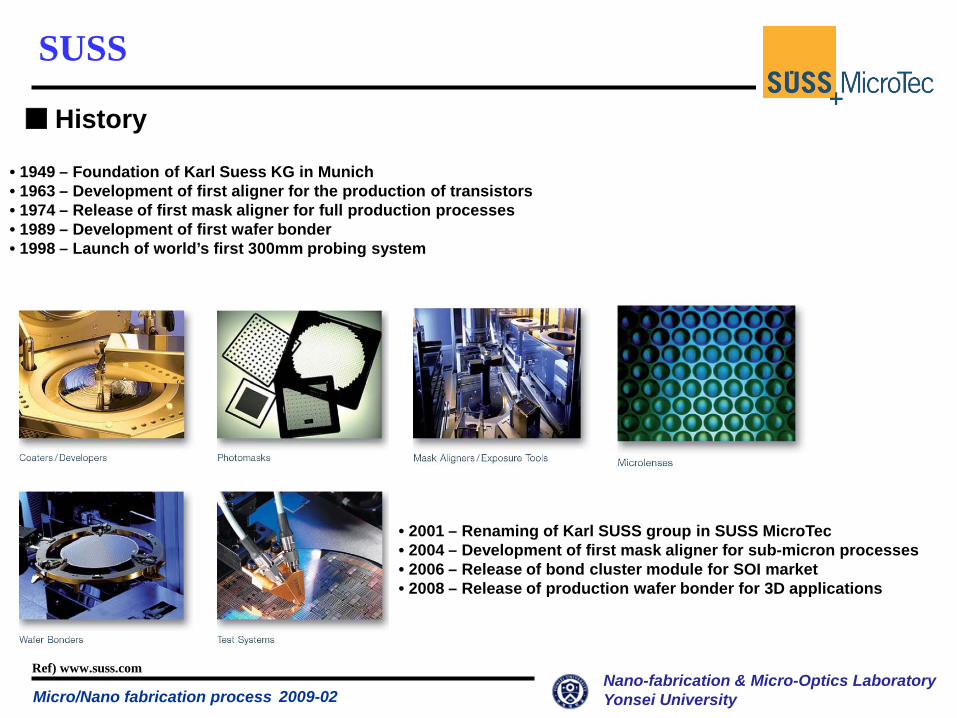
■ History
• 1949 – Foundation of Karl Suess KG in Munich• 1963 – Development of first aligner for the production of transistors• 1974 – Release of first mask aligner for full production processes• 1989 – Development of first wafer bonder• 1998 – Launch of world’s first 300mm probing system
• 2001 – Renaming of Karl SUSS group in SUSS MicroTec• 2004 – Development of first mask aligner for sub-micron processes• 2006 – Release of bond cluster module for SOI market• 2008 – Release of production wafer bonder for 3D applications
SUSS
Ref) www.suss.comNano-fabrication & Micro-Optics LaboratoryYonsei University

Micro/Nano fabrication process 2009-02
■ Products
• Lithography – Mask AlignerLithography ClustersPhotomask DesignAlignment VerificationWet ProcessingNanoimprint LithographySpin & Spray Coaters
• Wafer Bonder – Automated Bond ClusterSemi-Automated Wafer BondersManual Wafer BondersStand-Alone Related Tools
• Micro-optics – Refractive microlens arraysDiffractive Optics, DOE1D and 2D Diffuser
SUSS
Ref) www.suss.comNano-fabrication & Micro-Optics LaboratoryYonsei University

Micro/Nano fabrication process 2009-02
■ NPS 300 (Nano patterning stepper)
• Features
- NIL tool combining hot embossing and UV-NIL on wafer
- Possibility to add inert gas for faster print
- High accuracy and low volume fluid dispense
- Automatic stamp pick-up
- Manual or automated wafer loading / unloading
- Long-term stability and reliability
• Technical Data
- Imprinting Resolution : Sub-20nm- Alignment Accuracy : 100nm- Overlay Accuracy : 250nm
SUSS
Ref) www.suss.comNano-fabrication & Micro-Optics LaboratoryYonsei University
Micro/Nano fabrication process 2009-02
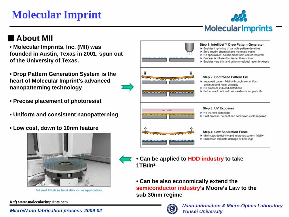
■About MII• Molecular Imprints, Inc. (MII) was founded in Austin, Texas in 2001, spun out of the University of Texas.
• Drop Pattern Generation System is the heart of Molecular Imprint’s advanced nanopatterning technology
• Precise placement of photoresist
• Uniform and consistent nanopatterning
• Low cost, down to 10nm feature
• Can be applied to HDD industry to take 1TB/in2
• Can be also economically extend the semiconductor industry’s Moore’s Law to the sub 30nm regime
Molecular Imprint
Ref) www.molecularimprints.comNano-fabrication & Micro-Optics LaboratoryYonsei University

Micro/Nano fabrication process 2009-02
■ Product• Imprio HD2200
Resolution: Sub-20nm, half-pitch for discrete track and bit patterned media
Throughput (double-sided): >150 disks per hour
Alignment: <10 microns (relative to disk spindle hole)
Disk Automation: Fully automated cassette-to-cassette and template loading
• Imprio HD1100
Resolution: Sub-50nm, half-pitch
Alignment: Not available
Flexibility: Can be configured to accept 25mm to 76mm substrates
Automation: Automated wafer and template loading
Molecular Imprint
Ref) www.molecularimprints.comNano-fabrication & Micro-Optics LaboratoryYonsei University

Micro/Nano fabrication process 2009-02
■ Product
• Perfecta TR1100
Resolution: Sub-50nm
Alignment: <10um (template to substrate)
Flexibility: Designed for 150mm synthetic quartz substrates
Automation: Automated wafer and template loading
• Imprio HD300
Resolution: Sub-32nm half pitch
Alignment: < 10nm, 3σ (single point, X,Y)
Automation: Fully automated wafer and mask loading
Flexibility: 200mm and 300mm substrates (SEMI standard)
Field size: 26mm x 32mm (step-and-scan compatible)
Throughput: Four wafers per hour
Molecular Imprint
Ref) www.molecularimprints.comNano-fabrication & Micro-Optics LaboratoryYonsei University

Micro/Nano fabrication process 2009-02
■ History• 2003 – NND established, NANOSISTM launch• 2004 – 30nm patterning with a silicon stamp• 2005/02 – Supplied NANOSIS 410 to ISRC in Seooul National University• 2005/06– Supplied NANOSIS 620 to Sogang University• 2005/08– Exhibition and operation at Nano Korea 2005
• 2005/10– Supplied NANOSIS 620 to LG Chem• 2005/11– Supplied NANOSIS 610 to Korea University• 2006/10– Supplied NANOSIS 420 to GIST• 2007/10– Supplied NANOSIS 830 to KOPTI• 2008/05– Supply over 10 sets NIL system in domestic market
Nano & Device
Ref) www.nanodevice.comNano-fabrication & Micro-Optics LaboratoryYonsei University

Micro/Nano fabrication process 2009-02
■ Product
• Nanosis 620
Economic price
Universal imprinter : UV curing, hot embossing
Near zero residual layer
Minimized footprint through a compact design
Excellent pattern uniformity
• Nanosis 820
Economic price
Universal imprinter : UV curing, hot embossing
Powerful alignment system
Near zero residual layer
Excellent pattern uniformity
Reduced process time
Nano & Device
Ref) www.nanodevice.comNano-fabrication & Micro-Optics LaboratoryYonsei University

Micro/Nano fabrication process 2009-02
EVG 社
• Precise wafer/substrate alignment for wafer bonding applications
• High-resolution bottom side splitfield microscope
• 1 µm alignment accuracy
• Easy to use Windows based operation
EVG 620 bond aligner
Nano-fabrication & Micro-Optics LaboratoryYonsei University

Micro/Nano fabrication process 2009-02
SUSS 社
NPS 300 (Nano patterning stepper)
..
• 250 nm overlay accuracy
• Unmatched sub-20 nm embossing capability
• Submicron Stamp-to-Wafer alignment with state-of-the-art pattern recognition system
Nano-fabrication & Micro-Optics LaboratoryYonsei University

Micro/Nano fabrication process 2009-02
Molecular Imprint 社
Imprio 250
• Resolution: Sub-50 nm
• Alignment: < 10 nm
• Flexibility: 200 mm and 300mm substrates with automated loading
• Field size: 26 x 32 mm active print area.
Nano-fabrication & Micro-Optics LaboratoryYonsei University

Micro/Nano fabrication process 2009-02
Nano & Device 社
Nanosis 610
• No align option
• Near zero residual layer
• UV curing & hot embossing (universal)
• Good pattern uniformity
• 6 inch direct imprinting
Nano-fabrication & Micro-Optics LaboratoryYonsei University

Micro/Nano fabrication process 2009-02
Issues of nanoimprinting
Thickness of residual layer
Large area patterning
Demolding
Imprinting material
Mass productivity and system itself
Fabrication of nano master / mold
Nano-fabrication & Micro-Optics LaboratoryYonsei University

Micro/Nano fabrication process 2009-02
Thickness of residual layer
Nano-fabrication & Micro-Optics LaboratoryYonsei University
Micro/Nano fabrication process 2009-02
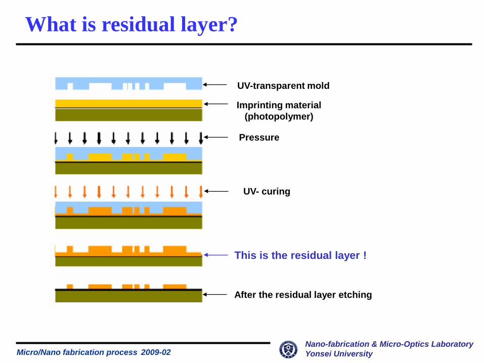
What is residual layer?
UV-transparent mold
Imprinting material (photopolymer)
Pressure
UV- curing
This is the residual layer !
After the residual layer etching
Nano-fabrication & Micro-Optics LaboratoryYonsei University

Micro/Nano fabrication process 2009-02
Importance of thickness of residual layer
Purpose of the nano imprinting lithography
• Use the pattern itself
- AR Surface- Optical nano grating- Wave guider- Nano structure for optoelectronic devices
• Use the pattern as a barrier for after process
- Replace the photolithography process
Nano-fabrication & Micro-Optics LaboratoryYonsei University

Micro/Nano fabrication process 2009-02
AR coating on mold
AR coating (Anti reflection coating)
Optical substrate has about 4% reflection in general
UV
Reflection of UV
Mold without AR coating
PHotopolymer
AR coating on mold surface is very important
Nano-fabrication & Micro-Optics LaboratoryYonsei University

Micro/Nano fabrication process 2009-02
Importance of thickness of residual layer
Nano structure for optoelectronic devices (MLA on VCSEL)
Rn1
VCSEL Micro-Lens Fiber
VCSEL array
Emitting area
Bonding padRn1
Rn1
We must control the residual layer for designed focal length
Nano-fabrication & Micro-Optics LaboratoryYonsei University

Micro/Nano fabrication process 2009-02
Importance of thickness of residual layer
Use the pattern as a barrier for after process (critical reason)
UV-transparent mold
photopolymer
Preparation Mold lamination andAppling pressure
UV curing
UV
Demolding
Remove the residual layer
Etch the substrate Remove the photopolymer
이때 pattern의크기에비해너무두꺼운 residual layer가남아있다면이를제거할때 pattern은모두손실되고만다
Nano-fabrication & Micro-Optics LaboratoryYonsei University

Micro/Nano fabrication process 2009-02
Zero residual layer process
Conventional imprint Zero residual imprint
Nano-fabrication & Micro-Optics LaboratoryYonsei University

Micro/Nano fabrication process 2009-02
Application of nano-imprinting technology I
Nano-fabrication & Micro-Optics LaboratoryYonsei University

Micro/Nano fabrication process 2009-02
연꽃잎
Super hydrophobic surface
자료출처: http://blog.empas.com/hl1vgt/, Manhui Sun, Langmuir, Vol.21, pp.8978, 2005 L. Feng, Advanced Material,Vol.14, pp.1857, 2002Alexander Otten, Langmuir, Vol.20, pp.2405, 2004
Nano-fabrication & Micro-Optics LaboratoryYonsei University

Micro/Nano fabrication process 2009-02
매미날개의모사
연꽃잎의모사 응용분야
<자동차>
<유리창>
Super hydrophobic surface
자료출처: Manhui Sun et at al.,langmuir, vol.21, pp.8978, 2005Woo Lee et at al., Langmuir, Vol.20, pp.7665, 2004http://www.dumitrup.com/blog/
Nano-fabrication & Micro-Optics LaboratoryYonsei University

Micro/Nano fabrication process 2009-02
나방의눈
Anti-reflective surface
자료출처: http://www.motheye.com/, http://blog.empas.com/squirrel1226/1Nano-fabrication & Micro-Optics LaboratoryYonsei University

Micro/Nano fabrication process 2009-02
무반사면의응용나방눈의모사패턴
Anti-reflective surface
자료출처: http://www.motheye.com/, http://www.nature.go.kr/insect/insectGuide/MNE’06 Micro- and Nano- EngineeringKenji Sogo, Journal of Photopolymer Science Technology, Vol.19, pp.647, 2006
Nano-fabrication & Micro-Optics LaboratoryYonsei University

Micro/Nano fabrication process 2009-02
상어의피부
Drag reduction of surface
Nano-fabrication & Micro-Optics LaboratoryYonsei University
자료출처: http://news.softpedia.com/news/The-Shark-Coating-42520.shtmlD. W. Bechert, Naturwissenschaften, Vol. 87, pp.157, 2004

Micro/Nano fabrication process 2009-02
<Speedo Fastskin II><Drag reduction of surface>
10% 감소효과
상어피부 상어피부형상의응용 -수영복
Drag reduction of surface
Nano-fabrication & Micro-Optics LaboratoryYonsei University
자료출처: http://www.speedo.com D. W. Bechert, Naturwissenschaften, Vol. 87, pp.157, 2004

Micro/Nano fabrication process 2009-02
Application of nano-imprinting technology II
Nano-fabrication & Micro-Optics LaboratoryYonsei University

Micro/Nano fabrication process 2009-02
Imprinting of bio chip
Bio chip fabrication using nano-imprinting
Nano-fabrication & Micro-Optics LaboratoryYonsei University
자료출처 : http://bmc.ub.uni-potsdam.de, http://www. macrogen.co.kr

Micro/Nano fabrication process 2009-02
Bio chip fabrication using nano-imprinting
Nano-fabrication & Micro-Optics LaboratoryYonsei University

Micro/Nano fabrication process 2009-02
LOC with microfluidic channels
Lab-on-a-chip fabrication using nano-imprinting
Nano-fabrication & Micro-Optics LaboratoryYonsei University
자료출처 : http://www.biodent.com, http://pubs.rsc.org