nanoelectromechanical switches (nem relays & nemfets) dimitrios tsamados adrian ionescu epfl...
TRANSCRIPT
Nanoelectromechanical Switches(NEM Relays & NEMFETs)
Dimitrios Tsamados Adrian Ionescu
EPFL
Kerem AkarvardarH.-S. Philip Wong
Stanford
Elad Alon Tsu-Jae King Liu
UC Berkeley

2
Outline
• Motivation • Device operation• Logic gate configurations• State-of-the-art • Scaling and performance• Issues• Conclusion
Part I: NEM Relays
Part II: NEMFETs

3
MotivationMotivationTwo key properties unavailable in CMOS
Zero Leakage
Zero static energy
Infinite subthreshold slope
Ultra-low VDD without degrading Ion
Ultra-low dynamic energy
Ultra-low energy operation beyond the capability of CMOS

4
MotivationExtra Motivation
• Hysteresis• Stiction
• Low temperature process
• High temperature operation• High radiation hardness
• Cheap substrates
SRAM and NV Memory
3-D integration andhybrid NEMS/CMOS
Niche applications
Reduced cost
Choi et al. IEDM 2007(UC Berkeley)
Chakraborty et al. IEEE Trans. Circ. Syst. 2007(Case Western Reserve U.)

5
Operation of the NEM Relay
OFF-state
S G D
ON-statePull-in
voltage, Vpi
= VDD,min
Pull-out voltage, Vpo
Nor
mal
ized
Pos
ition
VGS
1
3
2
0
Dra
in C
urre
ntVGS
S DG
insulating substrate
air gap
limit stop cantilever beam
Conventional Device Structure & Operation
infinite slopezero leakage
6
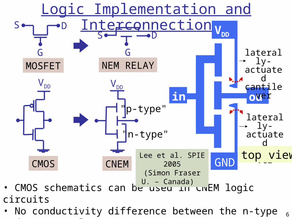
Operation of the NEM RelayLogic Implementation and Interconnection
• CMOS schematics can be used in CNEM logic circuits• No conductivity difference between the n-type and p-type relays• Simple layout enabling to small area
MOSFET NEM RELAY
CMOS CNEM
S D
G
S D
G
VDD VDD
in out
VDD
GND
laterally-actuated cantilever
laterally-actuated cantilever
Lee et al. SPIE 2005(Simon Fraser U. –
Canada)
"n-type"
"p-type"
top view

7
Operation of the NEM RelayEnergy-Reversible (ER) CNEM Logic Gates
Top View
Laterally-actuated ER CNEM Inverter
out = in
in
VD
D
GN
D
insu
lato
rca
ntile
ver
Elastic potential energy, which is stored due to beam bending, is reversibly used for switching
out = VDD
in = GND
GN
D
VD
Dout = GND
in = VDD
VD
D
GN
D
Akarvardar et al. DRC 2008
ER principle: Yang et al. MME 2003Delft University – The Netherlands

8
Operation of the NEM RelayEnergy-Reversible CNEM Logic Gates
Conventional
energy-reversible
floa
ting
el
ectr
ode
out = AB
A
VD
D
VD
D
GN
D
BERNANDGate
Pakula et al. (Delft U.) IEEE Sensors 2005
• Reduced VDD & dynamic energy (unless hysteresis is prevented) • Experimentally demonstrated in RF switches (VDD = 5 V instead of Vpi = 38 V)
• Any logic function can be realized
ER Relays:
Nor
mal
ized
Pos
ition
VGS
1
0VpiVpo0
(energy-reversible) (conventional)
VDD,min

9
State-of-the-ArtThe smallest 2-terminal switch ever reported:
Jang et al. APL 92, 2008(KAIST & Samsung – Korea)
• 15 nm gap • 35 nm beam thickness• TiN beam, sacrificial poly-Si, wet etch + critical point dry • Several hundred cycles endurance (insulator failure)
zero leakage
infinite slope
Vpo = 8 V Vpi = 13 V300 nm
10
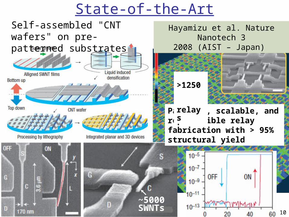
State-of-the-ArtHayamizu et al. Nature Nanotech 3
2008 (AIST – Japan)
Self-assembled "CNT wafers" on pre-patterned substrates
~5000 SWNTs
Parallel, scalable, and reproducible relay fabrication with > 95% structural yield
>1250 relays

11
• Scaling => smaller and faster relay that dissipates less energy• vdW Forces tend to become dominant at nanoscale
Constant-Field ScalingConstant-Field Scaling
1/KSpring constant
KResonance frequency
1/K2Elastic force
1/K2Electrostatic force
1/K3Pull-in energy
Resulting variation
Kvan der Waals forces
1/KPull-in delay
1/KPull-in voltage
1/K2Footprint area
1/KSupply voltage
1/KGap, thickness, length, widthScaled parameters
Scaling FactorParameter
1/KSpring constant
KResonance frequency
1/K2Elastic force
1/K2Electrostatic force
1/K3Pull-in energy
Resulting variation
Kvan der Waals forces
1/KPull-in delay
1/KPull-in voltage
1/K2Footprint area
1/KSupply voltage
1/KGap, thickness, length, widthScaled parameters
Scaling FactorParameter

12
Performance
Akarvardar et al. IEDM 2007
• 1 ns switching delay• 1.5 V supply voltage • 80 aJ switching energy• 0.03 μm2 lateral inverter area => competitive with CMOS• Zero leakage
S DGg0 = 10nm
L = 200 – 300 nm
h = 10 nm
L = 250 nm
siliconscaling
delay ↓Fvdw ↑
stiffer beams to compensate
for Fvdw
increased VDD
~ 1 ns
~ 1 V
Negligible Fvdw => 1 ns @ VDD 150 mV
4 nm

13
NEM relays vs. Low-Power CMOS
Lg = 45 nm LSTP CMOS (ITRS):
NEM relays should achieve nanosecond-range intrinsic delay @ VDD << 425 mV
=> Decrease the vdw forces substantially• How?
=> And/or operate close to the stiction limit• Increased sensitivity to device param.
Akarvardar et al. submitted to IEDM 2008
CV/I = 1 ns @ VDD = 425 mV
Zero leakage advantage of the NEM relay would only be apparent in logic circuits with relatively high device count and low activity
High VT (0.53 V) => Very low leakage (30 pA/μm)
14
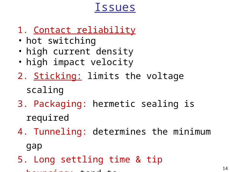
Issues
1. Contact reliability • hot switching • high current density • high impact velocity
2. Sticking: limits the voltage scaling
3. Packaging: hermetic sealing is required
4. Tunneling: determines the minimum gap
5. Long settling time & tip bouncing: tend to increase the switching delay
6. Brownian motion: leads to switching errors
15
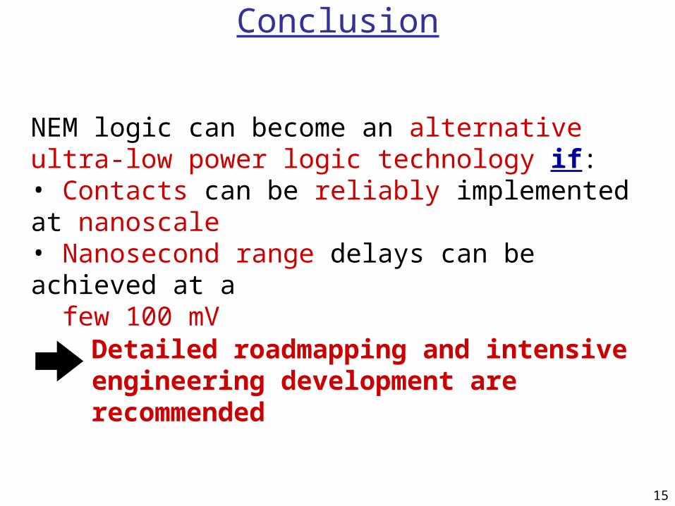
Conclusion
NEM logic can become an alternative ultra-low power logic technology if: • Contacts can be reliably implemented at nanoscale • Nanosecond range delays can be achieved at a few 100 mV
Detailed roadmapping and intensive engineering development are recommended

Nano-Electro-Mechanical FETs

17
Hybrid M/NEMS
Pure M/NEM devices:- micro/nano movable parts- passive device operation
Hybrid M/NEM devices:- micro/nano movable parts- solid state semiconductor device involved in operation
Drain
Source
Gate
Ex: suspended nano-beams Ex: suspended-gate FETs

18
M/NEM-FET: device architectures
Out-of-plane In-plane
Mov
e ga
teM
ove
body
Major advantages: new functionality and low power

19
20μm
Drain
Source
tgap = 220nm
Suspended-Gate
A
A’
• Resonant-Gate FET (Nathanson, 1966) • Suspended-Gate MOSFET (EPFL: A.M. Ionescu, ISQED 2001, IEDM 2005, 2006)• Nano-electro-mechanical FET (UC Berkeley, T.J. King, IEDM 2005)• Modeling of SG-FET (Stanford & EPFL: Akarvardar: IEEE TED 2008, Tsamados: SSE 2008)
movablegate
0 2 4 6 8 10 12 14
Gate voltage, VG(V)
Dra
in c
urre
nt, I
D
(A)
Pull-in
Pull-out
10-12
10-6
10-7
10-8
10-9
10-10
10-11
Experiment:Out-of-plane movable gate
Gate up:• high Vt
• in-series Cgap
Gate down • low Vt
• Cox
A
tkV gapo
inPull
3
Applications: power management, low power logic, memory
M/NEM-FET abrupt switch

20
NEMS simulation & modelingElectrostatic NEMS: mechanical & electrostatic analysis
Source: G. Li et al, Urbana-Champaign.

21
Simulation: 90nm NEM-FET
NEM-FET: scaling & simulation
• Multi-physics simulation for hybrid NEM device design• Coupled FEA: 2D ANSYS-DESSIS for suspended-gate FET
S D
SuspendedGate
S D
SuspendedGate

22
NEM-FET vs. MOSFET power management switch:• dynamic VT
• Ioff, Isubthreshold : 102 -104
• sleep area ~ MOSFET
Replaced by NEM-FET
NEM-FET power management switch

23
1.E-10
1.E-09
1.E-08
1.E-07
1.E-06
0 5 10 15 20VG (V)
I D (
A)
Mechanical pull-in
Mechanical pull-out
10-6
10-7
10-8
10-9
10-10
1
0
Drain
Source
Gate
• Electro-mechanical hysteresis: [ Vpull-in – Vpull-out ]• SG-MOSFET capacitor-less memory feasible• Hysteresis control! Scaling? Reliability?
N. Abelé et al., IEDM 2006
Hysteresis: 1T MEM-FET memory

24
Size & Voltage operation scaling (1)
• nanogap scaling (Samsung) tbeam= 20nmtgap = 20nm
NEM clamp switch with TiN beam memory cell array structure for high density non-volatile memory application
M.-S. Kim et al., ISDRS 2007

25
SG-FET compliant to ITRS 90nm node:tox=2nm, L=65nm, channel doping Nch=3×1018cm−3, μ0=278cm2/Vs , air-gap g0=5nm, W=400nm, h=10nm, Young modulus, E=170GPa.
VD=1.2V
Size & Voltage operation scaling (2)

26
• significant power savings (1-2 decades reduction) of inverter peak current
• no leakage power compared with nano-meter scaled CMOS inverter.
NEM-FET inverter

27
Movable/vibrating gate transistor
Laterally (in-plane) vibrating gate• lateral MOS transistor, detection in drain current• +4.3dB experimental gain demonstrated compared to capacitive detection using same structure
C. Durand et al., IEEE EDL 2008.
• e-beam defines gaps (~47nm gap resol.). • L=10m, W=165nm, d=120nm
LETI-CEA

28
D. Grogg, A.M. Ionescu, DRC 2008.
Laterally (in-plane) movable body:first demonstration of +30dB signal improvement
Double Gate switchable/vibrating body FET
EPFL
fres=2.4MHz, Q=6’000, Rm=200Ohm

29
D. Grogg, A.M. Ionescu,ESSDERC 2008, Confidential
Double Gate switchable/vibrating body FET
Experiment

30
• NEM-FET: true hybrid mechanical-solid-state switch with near-zero point subthreshold swing• attractive for low-Ioff power management switches, capacitor-less memory (D-RAM, S-RAM and NVM with appropriate storage layers) and new analog/RF functionality (in the resonant-gate configuration).• fabrication: compatibility of surface micromachining with CMOS processing.• Voltage scaling below 1-2V: nanogap technology• Size: ~as scalable as MOSFET (anchors needed) • NEMFET does not use mechanical contacts in the path of current flow: long-term reliability comparable to that of capacitive RF MEMS switches (>109 cycles), being limited by oxide charging.
Conclusion

31
MEMS/NEMS application roadmap in
crea
sin
g p
ow
er c
on
sum
pti
on
More transistorsthan MEMS devices
Nu
mb
er o
f T
ran
sist
ors
, NT
Number of Mechanical Components, NM
100
101
102
103
104
105
106
107
108
109
100 101 102 103 104 105 106 107 108 109
Early MEMS(sensing applications)
M/NEMSIntegration Levels
Enabled Applications
RF MEMSADXL
More MEMS devicesthan transistors
NT/NM=1
OMM 32x32
NEM-FET Power Gating and Embedded D/SRAM
Ultra-low-power NEM-based
Embedded NVM
IntegratedActuatorSystems
Ultra-low-power NEM Relay
Logic
AdaptiveOptics
Optical Switches& Aligners
Digital MicromirrorDevice (DMD)
CPU’s
incr
easi
ng
po
wer
co
nsu
mp
tio
nin
crea
sin
g p
ow
er c
on
sum
pti
on
More transistorsthan MEMS devices
Nu
mb
er o
f T
ran
sist
ors
, NT
Number of Mechanical Components, NM
100
101
102
103
104
105
106
107
108
109
100 101 102 103 104 105 106 107 108 109
Early MEMS(sensing applications)
M/NEMSIntegration Levels
Enabled Applications
RF MEMSADXL
More MEMS devicesthan transistors
NT/NM=1
OMM 32x32
NEM-FET Power Gating and Embedded D/SRAM
Ultra-low-power NEM-based
Embedded NVM
IntegratedActuatorSystems
Ultra-low-power NEM Relay
Logic
AdaptiveOptics
Optical Switches& Aligners
Digital MicromirrorDevice (DMD)
CPU’s
More transistorsthan MEMS devices
Nu
mb
er o
f T
ran
sist
ors
, NT
Number of Mechanical Components, NM
100
101
102
103
104
105
106
107
108
109
100 101 102 103 104 105 106 107 108 109
Early MEMS(sensing applications)
M/NEMSIntegration Levels
Enabled Applications
M/NEMSIntegration Levels
Enabled Applications
RF MEMSADXL
More MEMS devicesthan transistors
NT/NM=1
OMM 32x32
NEM-FET Power Gating and Embedded D/SRAM
Ultra-low-power NEM-based
Embedded NVM
IntegratedActuatorSystems
Ultra-low-power NEM Relay
Logic
AdaptiveOptics
Optical Switches& Aligners
Digital MicromirrorDevice (DMD)
CPU’s
NEM sensing

32
• NEMS Beyond CMOS = low power nano-switch More than Moore = new functionality
• Key role of NEMS for power savings and new functionality: future hybrid NEMS-CMOS
• Future role of true hybrid NEM-FET devices: abrupt switch, memory, resonator, sensing• Challenges for hybrid NEM-FET:
additional process control of nanoscale air-gap, thickness and uniformity of suspended structures, control and uniformity of mechanical properties fabrication: top-down & bottom-up (Si, CNTs) wafer-level packaging and reliability thermal drift
MEMS/NEMS application roadmap

33
Acknowledgments
EPFL: FP7 IST projects MIMOSA, MINAMI and NANO-RF
Stanford: DARPA, FCRP C2S2, NSF Roger T. Howe, David Elata, J Provine, Roozbeh Parsa, Kyeongran Yoo, Soogine Chong
UC Berkeley: DARPA, FCRP C2S2 Hei Kam