nanoelectronics roadmap for europe: from nanodevices and
TRANSCRIPT
HAL Id: cea-02186477https://hal-cea.archives-ouvertes.fr/cea-02186477
Submitted on 19 Nov 2020
HAL is a multi-disciplinary open accessarchive for the deposit and dissemination of sci-entific research documents, whether they are pub-lished or not. The documents may come fromteaching and research institutions in France orabroad, or from public or private research centers.
L’archive ouverte pluridisciplinaire HAL, estdestinée au dépôt et à la diffusion de documentsscientifiques de niveau recherche, publiés ou non,émanant des établissements d’enseignement et derecherche français ou étrangers, des laboratoirespublics ou privés.
NanoElectronics roadmap for Europe : Fromnanodevices and innovative materials to system
integrationJ. Ahopelto, G. Ardila, L. Baldi, F. Balestra, Didier Belot, G. Fagas, S. de
Gendt, D. Demarchi, M. Fernandez-Bolanos, D. Holden, et al.
To cite this version:J. Ahopelto, G. Ardila, L. Baldi, F. Balestra, Didier Belot, et al.. NanoElectronics roadmap forEurope : From nanodevices and innovative materials to system integration. Solid-State Electronics,Elsevier, 2019, 155, pp.7-19. �10.1016/j.sse.2019.03.014�. �cea-02186477�

NanoElectronics Roadmap for Europe:
From Nanodevices and Innovative Materials to
System Integration J. Ahopelto, VTT Technical Research Centre of Finland
Ltd, Espoo, Finland, [email protected]
G. Ardila, U. Grenoble Alpes, CNRS, Grenoble INP, IMEP-
LaHC, Grenoble, France, [email protected]
L. Baldi, Consultant, Milano, Italy, [email protected],
F. Balestra, U. Grenoble Alpes, CNRS, Grenoble INP, IMEP-
LaHC, Grenoble, France, [email protected],
D. Belot, LETI, Grenoble, France, [email protected]
G. Fagas, Tyndall, Cork, Ireland, [email protected]
S. De Gendt, IMEC, Leuven, Belgium, Ste-
D. Demarchi, Politecnico di Torino and IUNET, Torino,
Italy, [email protected]
M. Fernandez-Bolaños, Lausanne, Switzerland,
D. Holden, LETI, Grenoble, France, [email protected]
A. Ionescu, EPFL, Lausanne, Switzerland,
G. Meneghesso, University of Padova and IUNET, Padova,
Italy, [email protected]
A. Mocuta, IMEC, Leuven, Belgium, an-
M. Pfeffer, Fraunhofer IISB, Erlangen, mar-
R. M. Popp, edacentrum GmbH, Hannover, Germany,
E. Sangiorgi, University of Bologna and IUNET, Bologna,
Italy, [email protected]
C. M. Sotomayor Torres, ICN2 and ICREA, Barcelona,
Spain, [email protected]
Abstract—The NEREID project (“NanoElectronics Roadmap for
Europe: Identification and Dissemination”) is dedicated to map
the future of European Nanoelectronics. NEREID’s objective is
to develop a medium and long term roadmap for the European
nanoelectronics industry, starting from the needs of applications
to address societal challenges and leveraging the strengths of the
European eco-system. In addition, it will lead to an early bench-
mark/identification of promising novel nanoelectronic technolo-
gies, based on the advanced concepts developed by Research Cen-
tres and Universities, and an identification of bottlenecks all
along the innovation (value) chain. Considering applications like
Energy, Automotive, Medical/Life Science, Security, loT, Mobile
Convergence and Digital Manufacturing the NEREID roadmap
is about Advanced Logic and Connectivity, Functional Diversifi-
cation (Smart Sensors, Smart Energy and Energy for Autono-
mous Systems), Beyond-CMOS, Heterogeneous Integration and
System Design as well as Equipment, Materials and Manufactur-
ing Science. This article gives an overview on the roadmap’s
structure and content.
Keywords: Nanoelectronics, Roadmap, Beyond CMOS, More
Moore, More than Moore, Design-technology gap, Heterogeneous
integration, System design, Novel materials, Equipments and
manufacturing.
I. INTRODUCTION
Roadmaps are strongly needed for all high tech sectors, like Nanoelectronics, to improve links between academic and in-dustrial research, to drive investments, to provide inputs for fu-ture research programmes and to coordinate efforts to over-come the main technology challenges.
For more than 20 years, the International Technology Roadmap for Semiconductors has helped the industry to follow
Moore’s Law, with a constant reduction in device costs and an exponential growth in semiconductor market. The main role of ITRS has been in providing research guidance for the many ac-tors of the semiconductor ecosystem, in synchronizing the technology development and the timely availability of manu-facturing equipment and methods and in providing focus on critical bottlenecks.
However, the “technology push” that has been at the base of ITRS has shown in the latest years its limits: device size and speed are no longer the only parameters of importance, and system-driven technologies have been considered by the new IRDS Roadmap (International Roadmap for Devices and Sys-tems), focusing on computing systems.
On the other hand, the integration of new functionalities, required by new applications, needs the incorporation of spe-cial metrics for technologies that do not necessarily scale ac-cording to "Moore's Law“, expanding the focus from chips to different kinds of systems. This trend is especially relevant for the European semiconductor industry that has focused on seg-ments of greater relevance for the European applications indus-try, like Automotive, Industrial and Medical. Therefore, an ap-propriate kind of roadmap is needed for Europe which focuses on nanoelectronics with respect to the European abilities and strength.
The NEREID roadmap for European Nanoelectronics co-vers both application and technology sectors. This comprises applications in the field of Energy, Automotive, Medical/Life Science, Security, loT, Mobile Convergence and Digital Manu-facturing as well as technologies like Advanced Logic and Connectivity, Functional Diversification (Smart Sensors, Smart Energy and Energy for Autonomous Systems), Beyond-CMOS,
Heterogeneous Integration and System Design and Equipment, Materials and Manufacturing Science.
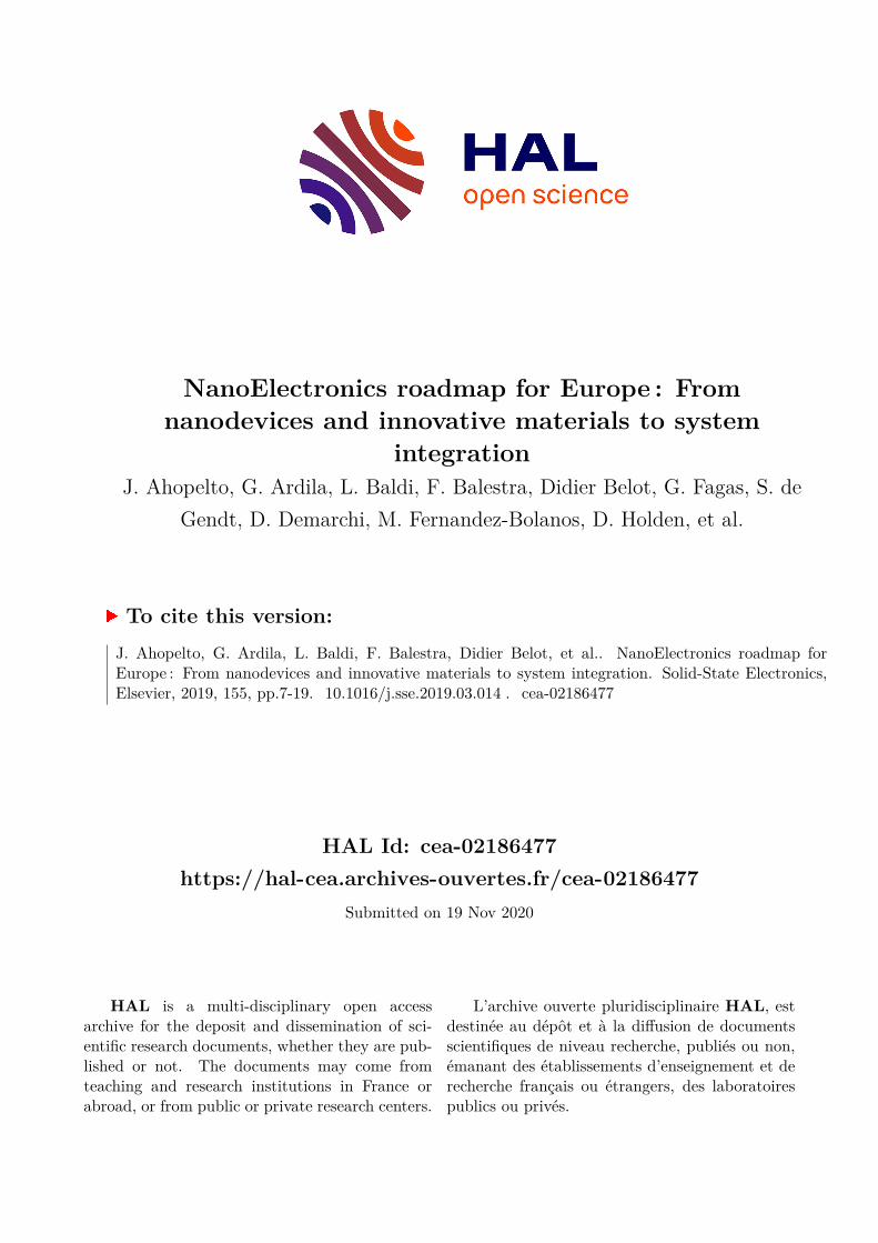
With its mid/long term focus, the NEREID Roadmap is complementary to the European ECSEL ECS Strategic Re-search Agenda, which is focusing on shorter term horizons. Nevertheless, NEREID has also developed collaboration with, and is in part complementary to, the new International Roadmap for Devices and Systems (IRDS) in the Europe-led More than Moore domain (e.g. Smart Sensors, Energy, Energy Harvesting) leading to beyond-computing systems (s. Figure 1. ).
Figure 1. NEREID Roadmap Objective
The important assets of NEREID are the following:
• the projection of the evolution of many Figures of Merit (FoMs) vs time for covering the most promising tech-nologies including novel functionalities
• the understanding of the dependencies between short/ medium term (e.g. More Moore and More than Moore) and long/very long term (e.g. Beyond CMOS) activities
• the strong interaction between application and technolo-gy experts, coming from leading research players in in-dustry and academia, especially with the organization of many Workshops.
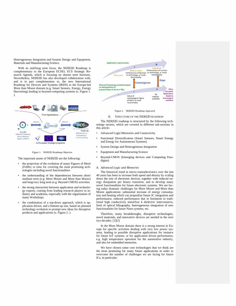
• the combination of a top-down approach, which is ap-plication driven, and a bottom-up one, based on planned technology evolution to prompt new ideas for disruptive products and applications (s. Figure 2. ).
Figure 2. NEREID Roadmap Approach
II. STRUCTURE OF THE NEREID ROADMAP
The NEREID roadmap is structured by the following tech-nology sectors, which are covered in different sub-sections in this article:
• Advanced Logic/Memories and Connectivity
• Functional Diversification (Smart Sensors, Smart Energy and Energy for Autonomous Systems)
• System Design and Heterogeneous Integration
• Equipment and Manufacturing Science
• Beyond-CMOS (Emerging devices and Computing Para-digms)
A. Advanced Logic and Memories
The historical trend in micro-/nanoelectronics over the last 40 years has been to increase both speed and density by scaling down the size of electronic devices, together with reduced en-ergy dissipation per binary transition, and to develop many novel functionalities for future electronic systems. We are fac-ing today dramatic challenges for More Moore and More than Moore applications: substantial increase of energy consump-tion and heating which can jeopardize future IC integration and performance, reduced performance due to limitation in tradi-tional high conductivity metal/low k dielectric interconnects, limit of optical lithography, heterogeneous integration of new functionalities for future Nano systems, etc.
Therefore, many breakthroughs, disruptive technologies, novel materials, and innovative devices are needed in the next two decades. [1][2]
In the More Moore domain there is a strong interest in Eu-rope for specific activities dealing with very low power sys-tems, leading to possible disruptive applications for instance for future IoT systems, or for application driven performance, e.g. high temperature operation for the automotive industry, and also for embedded memories.
We have chosen some core technologies that we think are the most promising for many future applications in order to overcome the number of challenges we are facing for future ICs, in particular:
• High performance
• Low/very low static and dynamic power consumption
• Device scaling
• Low variability
• Affordable cost
Considering these challenges, the following nanodevices and technologies have been considered as very relevant for fu-ture Nanoscale FETs:
• FD (Fully Depleted) SOI (Silicon-On-Insulator) MOSFET: for low power applications and low variability
• FinFET (or Trigate FET): for high performance and/or low power applications
• Nanowire FET: for high performance and low power appli-cations and ultimate integration
• CNTFET/Carbon NanoTube FET: for very fast and possi-bly ultimately scaled transistors for logic applications, with self-assembly based fabrication
• NCFET/Negative Capacitance FET: for very low power application using steep subthreshold slope
• Non-charge-based Resistive Memories or alternative charge-based Memories: to replace charge-based memories using PCRAM (Phase Change RAM), RRAM (Resistive RAM using a nanofilament), MRAM (Magnetic RAM, es-pecially STT/Spin Transfer Torque MRAM), or FeRAM or FeFET (using the polarization of a ferroelectric material)
• Sequential 3D integration: for increasing device integration (transistors, memories, sensors, etc.) and performance using 3D stacking
The roadmap also covers the future modelling and charac-terization tools needed for developing these future devices and technologies.
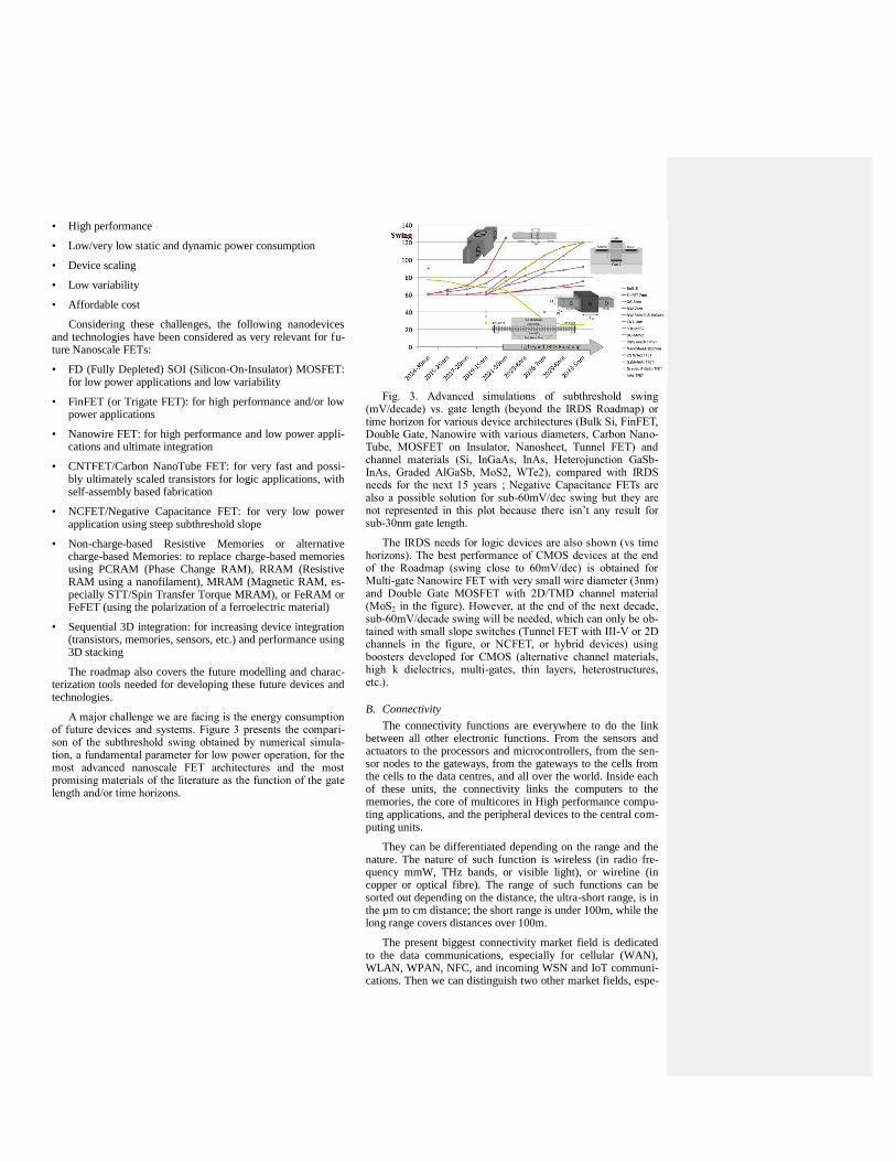
A major challenge we are facing is the energy consumption of future devices and systems. Figure 3 presents the compari-son of the subthreshold swing obtained by numerical simula-tion, a fundamental parameter for low power operation, for the most advanced nanoscale FET architectures and the most promising materials of the literature as the function of the gate length and/or time horizons.
Fig. 3. Advanced simulations of subthreshold swing (mV/decade) vs. gate length (beyond the IRDS Roadmap) or time horizon for various device architectures (Bulk Si, FinFET, Double Gate, Nanowire with various diameters, Carbon Nano-Tube, MOSFET on Insulator, Nanosheet, Tunnel FET) and channel materials (Si, InGaAs, InAs, Heterojunction GaSb-InAs, Graded AlGaSb, MoS2, WTe2), compared with IRDS needs for the next 15 years ; Negative Capacitance FETs are also a possible solution for sub-60mV/dec swing but they are not represented in this plot because there isn’t any result for sub-30nm gate length.
The IRDS needs for logic devices are also shown (vs time horizons). The best performance of CMOS devices at the end of the Roadmap (swing close to 60mV/dec) is obtained for Multi-gate Nanowire FET with very small wire diameter (3nm) and Double Gate MOSFET with 2D/TMD channel material (MoS2 in the figure). However, at the end of the next decade, sub-60mV/decade swing will be needed, which can only be ob-tained with small slope switches (Tunnel FET with III-V or 2D channels in the figure, or NCFET, or hybrid devices) using boosters developed for CMOS (alternative channel materials, high k dielectrics, multi-gates, thin layers, heterostructures, etc.).
B. Connectivity
The connectivity functions are everywhere to do the link between all other electronic functions. From the sensors and actuators to the processors and microcontrollers, from the sen-sor nodes to the gateways, from the gateways to the cells from the cells to the data centres, and all over the world. Inside each of these units, the connectivity links the computers to the memories, the core of multicores in High performance compu-ting applications, and the peripheral devices to the central com-puting units.
They can be differentiated depending on the range and the nature. The nature of such function is wireless (in radio fre-quency mmW, THz bands, or visible light), or wireline (in copper or optical fibre). The range of such functions can be sorted out depending on the distance, the ultra-short range, is in the µm to cm distance; the short range is under 100m, while the long range covers distances over 100m.
The present biggest connectivity market field is dedicated to the data communications, especially for cellular (WAN), WLAN, WPAN, NFC, and incoming WSN and IoT communi-cations. Then we can distinguish two other market fields, espe-
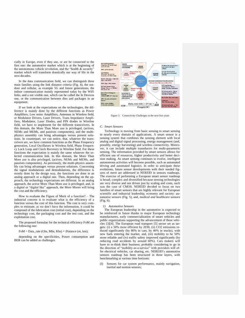
cially in Europe, even if they use, or are be connected to the first one: the automotive market which is at the beginning of the autonomous vehicle revolution, and the “health & security” market which will transform drastically our way of life in the next decades.
In the data communication field, we can distinguish three main families using the link distance criteria (Fig. 4), the out-door and cellular, as example 5G and future generations, the indoor communication mainly represented today by the WiFi links, and a not visible one, which can be called the In Devices one, or the communication between dies and packages in an equipment.
If we look at the expectations on the technologies, the dif-ference is mainly done by the different functions as Power Amplifiers, Low noise Amplifiers, Antennas in Wireless field, or Modulator Drivers, Laser Drivers, Trans Impedance Ampli-fiers, Modulator, Laser Diodes, and PIN diodes in Wireline field, we have to implement for the different transceivers. In this domain, the More Than More axe is privileged, (actives, NEMs and MEMs, and passives components), and the multi-physics assembly can bring advantages versus present solu-tions. In counterpart, we can notice, that, whatever the trans-ceivers are, we have common functions as the Phase Frequency generation, Local Oscillators in Wireless field, Phase Frequen-cy Lock Loop and Clock Recovery in Wireline field. For these functions the expectation is mainly the same whatever the se-lected communication link. In this domain, the More Than More axe is also privileged, (actives, NEMs and MEMs, and passives components). As previously, the multi-physics assem-bly can bring advantages versus present solutions. Concerning the signal modulations and demodulations, the difference is mostly done by the design way, the functions are done in an analog approach or a digital one. Then, depending on the ap-proach, the technology expectations are different. In an analog approach, the active More Than More axe is privileged, and, in a digital or “digital like” approach, the More Moore will bring the cost and the efficiency.
How to evaluate the Figure of Merit of a function? – The industrial concern is to evaluate what is the efficiency of a function versus the cost of this function. The cost is very com-plex to estimate, as we don’t have the information, it could be composed of the fabrication cost (initial cost), depending on the technology cost, the packaging cost and the test cost, and the exploitation cost.
The proposed formulae for the technical efficiency FoM are the following one:
FoM = Data_rate (Gbs, Mbs, Kbs) × 𝐷istance (𝑚, km);
depending on the specificities, Power consumption and BER can be added as challenges.
Figure 3. Connectivity Challenges in the next five years
C. Smart Sensors
Technology is moving from basic sensing to smart sensing in nearly every domain of applications. A smart sensor is a sensing system that combines the sensing element with local analog and digital signal processing, energy management (and, possibly, energy harvesting) and wireless connectivity. Moreo-ver, it can include multiple transducers for multi-parametric sensing. The information provided by smart sensors allows for efficient use of resources, higher productivity and better deci-sion making. As smart sensing continues to evolve, intelligent autonomous activities will become possible, such as automated driving and automated logistics. In order to anticipate these evolutions, future sensor developments with their needed fig-ures of merit are addressed in NEREID in sensors roadmaps. The exercise of performing a European smart sensor roadmap is broad, complex and diversified because sensing technologies are very diverse and not driven just by scaling and costs, such was the case of CMOS. NEREID decided to focus on two families of smart sensors that are highly relevant for European scientific and industrial leadership, economy and society: au-tomotive sensors (Fig. 5), and, medical and healthcare sensors (Fig. 6).
1) Automotive Sensors The European leadership in the automotive is expected to
be reinforced in future thanks to major European technology manufacturers, early commercialization of smart vehicles and public organizations supporting the advancement of these vehi-cles [3][4]. The European road transport [5] sector set as tar-gets: (i) a 50% more efficient by 2030, (ii) CO2 emissions re-duced significantly (by 80% in cars, by 40% in trucks), with new fuels entering the market, and, (iii) mobility to be 50% more reliable and (iv) traffic safety improved significantly (by reducing road accidents by around 60%). Cars makers will have to re-think their business; probably considering to go in the direction of “mobility-as-a-service” with providers will of-fer electrical vehicles, car sharing, etc. NEREID’s automotive sensors roadmap has been structured in three layers, with benchmarking at various time horizons:
(I) Sensors for car system performance, mainly navigation, inertial and motion sensors;
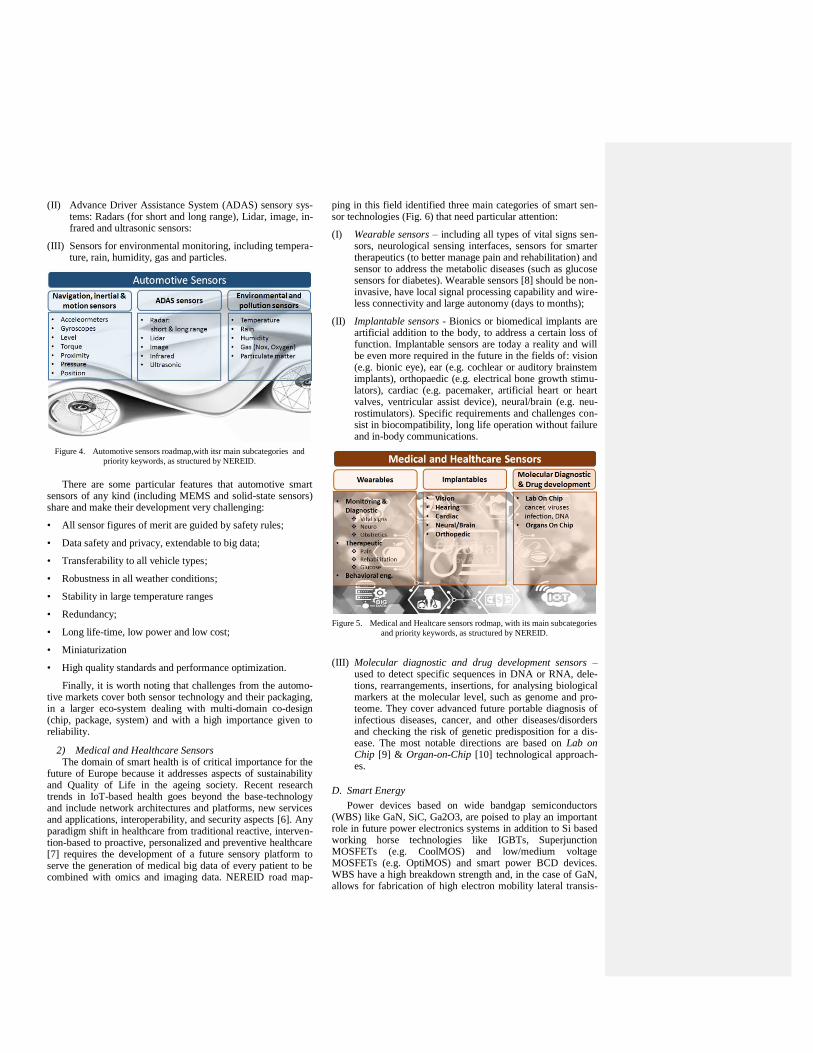
(II) Advance Driver Assistance System (ADAS) sensory sys-tems: Radars (for short and long range), Lidar, image, in-frared and ultrasonic sensors:
(III) Sensors for environmental monitoring, including tempera-ture, rain, humidity, gas and particles.
Figure 4. Automotive sensors roadmap,with itsr main subcategories and
priority keywords, as structured by NEREID.
There are some particular features that automotive smart sensors of any kind (including MEMS and solid-state sensors) share and make their development very challenging:
• All sensor figures of merit are guided by safety rules;
• Data safety and privacy, extendable to big data;
• Transferability to all vehicle types;
• Robustness in all weather conditions;
• Stability in large temperature ranges
• Redundancy;
• Long life-time, low power and low cost;
• Miniaturization
• High quality standards and performance optimization.
Finally, it is worth noting that challenges from the automo-tive markets cover both sensor technology and their packaging, in a larger eco-system dealing with multi-domain co-design (chip, package, system) and with a high importance given to reliability.
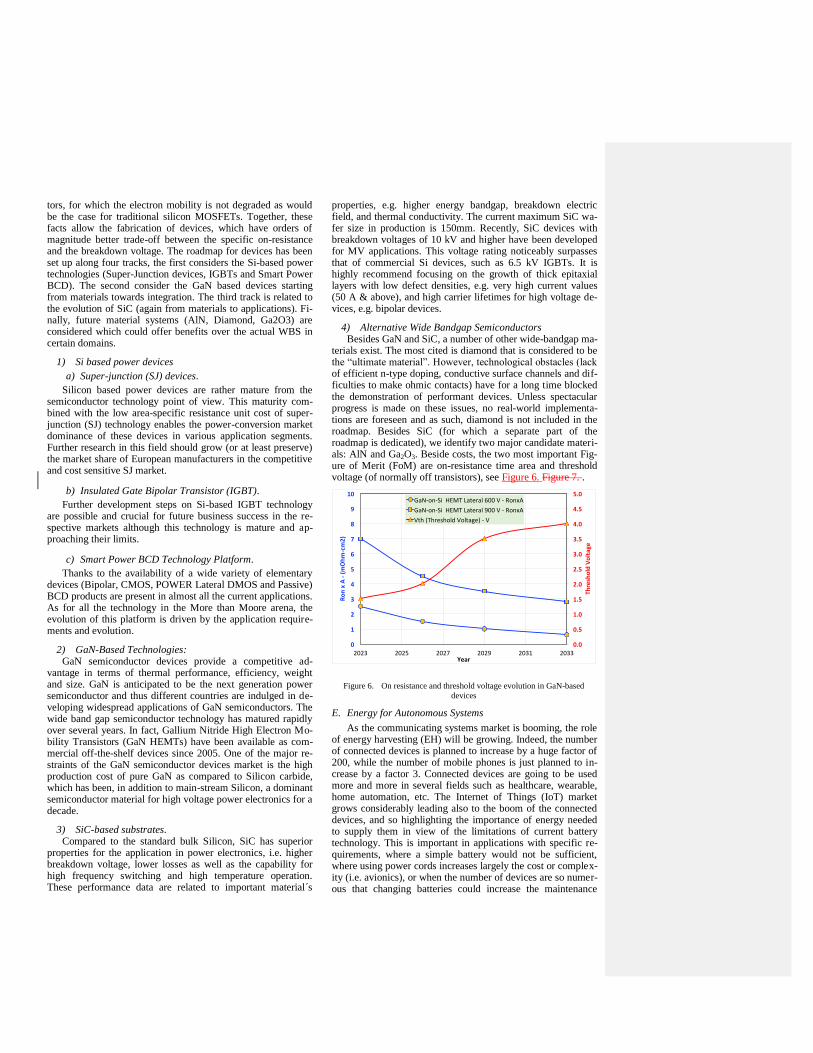
2) Medical and Healthcare Sensors The domain of smart health is of critical importance for the
future of Europe because it addresses aspects of sustainability and Quality of Life in the ageing society. Recent research trends in IoT-based health goes beyond the base-technology and include network architectures and platforms, new services and applications, interoperability, and security aspects [6]. Any paradigm shift in healthcare from traditional reactive, interven-tion-based to proactive, personalized and preventive healthcare [7] requires the development of a future sensory platform to serve the generation of medical big data of every patient to be combined with omics and imaging data. NEREID road map-
ping in this field identified three main categories of smart sen-sor technologies (Fig. 6) that need particular attention:
(I) Wearable sensors – including all types of vital signs sen-sors, neurological sensing interfaces, sensors for smarter therapeutics (to better manage pain and rehabilitation) and sensor to address the metabolic diseases (such as glucose sensors for diabetes). Wearable sensors [8] should be non-invasive, have local signal processing capability and wire-less connectivity and large autonomy (days to months);
(II) Implantable sensors - Bionics or biomedical implants are artificial addition to the body, to address a certain loss of function. Implantable sensors are today a reality and will be even more required in the future in the fields of: vision (e.g. bionic eye), ear (e.g. cochlear or auditory brainstem implants), orthopaedic (e.g. electrical bone growth stimu-lators), cardiac (e.g. pacemaker, artificial heart or heart valves, ventricular assist device), neural/brain (e.g. neu-rostimulators). Specific requirements and challenges con-sist in biocompatibility, long life operation without failure and in-body communications.
Figure 5. Medical and Healtcare sensors rodmap, with its main subcategories
and priority keywords, as structured by NEREID.
(III) Molecular diagnostic and drug development sensors –used to detect specific sequences in DNA or RNA, dele-tions, rearrangements, insertions, for analysing biological markers at the molecular level, such as genome and pro-teome. They cover advanced future portable diagnosis of infectious diseases, cancer, and other diseases/disorders and checking the risk of genetic predisposition for a dis-ease. The most notable directions are based on Lab on Chip [9] & Organ-on-Chip [10] technological approach-es.
D. Smart Energy
Power devices based on wide bandgap semiconductors (WBS) like GaN, SiC, Ga2O3, are poised to play an important role in future power electronics systems in addition to Si based working horse technologies like IGBTs, Superjunction MOSFETs (e.g. CoolMOS) and low/medium voltage MOSFETs (e.g. OptiMOS) and smart power BCD devices. WBS have a high breakdown strength and, in the case of GaN, allows for fabrication of high electron mobility lateral transis-
tors, for which the electron mobility is not degraded as would be the case for traditional silicon MOSFETs. Together, these facts allow the fabrication of devices, which have orders of magnitude better trade-off between the specific on-resistance and the breakdown voltage. The roadmap for devices has been set up along four tracks, the first considers the Si-based power technologies (Super-Junction devices, IGBTs and Smart Power BCD). The second consider the GaN based devices starting from materials towards integration. The third track is related to the evolution of SiC (again from materials to applications). Fi-nally, future material systems (AlN, Diamond, Ga2O3) are considered which could offer benefits over the actual WBS in certain domains.
1) Si based power devices
a) Super-junction (SJ) devices.
Silicon based power devices are rather mature from the semiconductor technology point of view. This maturity com-bined with the low area-specific resistance unit cost of super-junction (SJ) technology enables the power-conversion market dominance of these devices in various application segments. Further research in this field should grow (or at least preserve) the market share of European manufacturers in the competitive and cost sensitive SJ market.
b) Insulated Gate Bipolar Transistor (IGBT).
Further development steps on Si-based IGBT technology are possible and crucial for future business success in the re-spective markets although this technology is mature and ap-proaching their limits.
c) Smart Power BCD Technology Platform.
Thanks to the availability of a wide variety of elementary devices (Bipolar, CMOS, POWER Lateral DMOS and Passive) BCD products are present in almost all the current applications. As for all the technology in the More than Moore arena, the evolution of this platform is driven by the application require-ments and evolution.
2) GaN-Based Technologies: GaN semiconductor devices provide a competitive ad-
vantage in terms of thermal performance, efficiency, weight and size. GaN is anticipated to be the next generation power semiconductor and thus different countries are indulged in de-veloping widespread applications of GaN semiconductors. The wide band gap semiconductor technology has matured rapidly over several years. In fact, Gallium Nitride High Electron Mo-bility Transistors (GaN HEMTs) have been available as com-mercial off-the-shelf devices since 2005. One of the major re-straints of the GaN semiconductor devices market is the high production cost of pure GaN as compared to Silicon carbide, which has been, in addition to main-stream Silicon, a dominant semiconductor material for high voltage power electronics for a decade.
3) SiC-based substrates. Compared to the standard bulk Silicon, SiC has superior
properties for the application in power electronics, i.e. higher breakdown voltage, lower losses as well as the capability for high frequency switching and high temperature operation. These performance data are related to important material´s
properties, e.g. higher energy bandgap, breakdown electric field, and thermal conductivity. The current maximum SiC wa-fer size in production is 150mm. Recently, SiC devices with breakdown voltages of 10 kV and higher have been developed for MV applications. This voltage rating noticeably surpasses that of commercial Si devices, such as 6.5 kV IGBTs. It is highly recommend focusing on the growth of thick epitaxial layers with low defect densities, e.g. very high current values (50 A & above), and high carrier lifetimes for high voltage de-vices, e.g. bipolar devices.
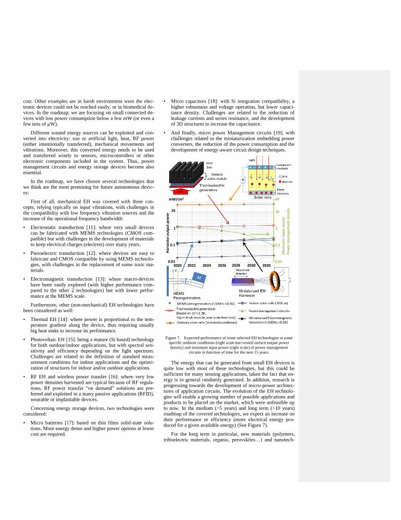
4) Alternative Wide Bandgap Semiconductors Besides GaN and SiC, a number of other wide-bandgap ma-
terials exist. The most cited is diamond that is considered to be the “ultimate material”. However, technological obstacles (lack of efficient n-type doping, conductive surface channels and dif-ficulties to make ohmic contacts) have for a long time blocked the demonstration of performant devices. Unless spectacular progress is made on these issues, no real-world implementa-tions are foreseen and as such, diamond is not included in the roadmap. Besides SiC (for which a separate part of the roadmap is dedicated), we identify two major candidate materi-als: AlN and Ga2O3. Beside costs, the two most important Fig-ure of Merit (FoM) are on-resistance time area and threshold voltage (of normally off transistors), see Figure 6. Figure 7. .
Figure 6. On resistance and threshold voltage evolution in GaN-based
devices
E. Energy for Autonomous Systems
As the communicating systems market is booming, the role of energy harvesting (EH) will be growing. Indeed, the number of connected devices is planned to increase by a huge factor of 200, while the number of mobile phones is just planned to in-crease by a factor 3. Connected devices are going to be used more and more in several fields such as healthcare, wearable, home automation, etc. The Internet of Things (IoT) market grows considerably leading also to the boom of the connected devices, and so highlighting the importance of energy needed to supply them in view of the limitations of current battery technology. This is important in applications with specific re-quirements, where a simple battery would not be sufficient, where using power cords increases largely the cost or complex-ity (i.e. avionics), or when the number of devices are so numer-ous that changing batteries could increase the maintenance
0.0
0.5
1.0
1.5
2.0
2.5
3.0
3.5
4.0
4.5
5.0
0
1
2
3
4
5
6
7
8
9
10
2023 2025 2027 2029 2031 2033
ThresholdVoltage
RonxA-(mOhm-cm2)
Year
GaN-on-SiHEMTLateral600V-RonxA
GaN-on-SiHEMTLateral900V-RonxA
Vth(ThresholdVoltage)-V
cost. Other examples are in harsh environment were the elec-tronic devices could not be reached easily, or in biomedical de-vices. In the roadmap, we are focusing on small connected de-vices with low power consumption below a few mW (or even a few tens of µW).
Different wasted energy sources can be exploited and con-verted into electricity: sun or artificial light, heat, RF power (either intentionally transferred), mechanical movements and vibrations. Moreover, this converted energy needs to be used and transferred wisely to sensors, microcontrollers or other electronic components included in the system. Thus, power management circuits and energy storage devices become also essential.
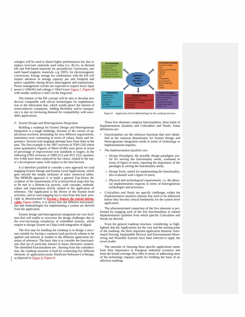
In the roadmap, we have chosen several technologies that we think are the most promising for future autonomous devic-es:
First of all, mechanical EH was covered with three con-cepts, relying typically on input vibrations, with challenges in the compatibility with low frequency vibration sources and the increase of the operational frequency bandwidth:
• Electrostatic transduction [11]: where very small devices can be fabricated with MEMS technologies (CMOS com-patible) but with challenges in the development of materials to keep electrical charges (electrets) over many years.
• Piezoelectric transduction [12]: where devices are easy to fabricate and CMOS compatible by using MEMS technolo-gies, with challenges in the replacement of some toxic ma-terials.
• Electromagnetic transduction [13]: where macro-devices have been vastly explored (with higher performance com-pared to the other 2 technologies) but with lower perfor-mance at the MEMS scale.
Furthermore, other (non-mechanical) EH technologies have been considered as well:
• Thermal EH [14]: where power is proportional to the tem-perature gradient along the device, thus requiring usually big heat sinks to increase its performance.
• Photovoltaic EH [15]: being a mature (Si based) technology for both outdoor/indoor applications, but with spectral sen-sitivity and efficiency depending on the light spectrum. Challenges are related to the definition of standard meas-urement conditions for indoor applications and the optimi-zation of structures for indoor and/or outdoor applications.
• RF EH and wireless power transfer [16]: where very low power densities harvested are typical because of RF regula-tions, RF power transfer “on demand” solutions are pre-ferred and exploited in a many passive applications (RFID), wearable or implantable devices.
Concerning energy storage devices, two technologies were considered:
• Micro batteries [17]: based on thin films solid-state solu-tions. More energy dense and higher power options at lower cost are required.
• Micro capacitors [18]: with Si integration compatibility, a higher robustness and voltage operation, but lower capaci-tance density. Challenges are related to the reduction of leakage currents and series resistance, and the development of 3D structures to increase the capacitance.
• And finally, micro power Management circuits [19], with challenges related to the miniaturization embedding power converters, the reduction of the power consumption and the development of energy-aware circuit design techniques.
Figure 7. Expected performance of some selected EH technologies at some
specific ambient conditions (right scale-har-vested surface output power
density) and minimum input power (right scale) of power management
circuits in function of time for the next 15 years.
The energy that can be generated from small EH devices is quite low with most of these technologies, but this could be sufficient for many sensing applications, taken the fact that en-ergy is in general randomly generated. In addition, research is progressing towards the development of micro-power architec-tures of application circuits. The evolution of the EH technolo-gies will enable a growing number of possible applications and products to be placed on the market, which were unfeasible up to now. In the medium (>5 years) and long term (>10 years) roadmap of the covered technologies, we expect an increase on their performance or efficiency (more electrical energy pro-duced for a given available energy) (See Figure 7).
For the long term in particular, new materials (polymers, triboelectric materials, organic, perovskites…) and nanotech-
nologies will be used to obtain higher performances but also to replace toxic/rare materials used today (i.e. Bi2Te3 in thermal EH and Pub-based materials for piezoelectric conversion, rare earth based magnetic materials, e.g. DfES, for electromagnetic conversion). Energy storage for combination with the EH will require advances in storage capacity per unit footprint and power capability during device interrogation and transmission. Power management circuits are expected to require lower input power (<100nW) and voltage (<10mV) (see Figure 7. Figure 8) with smaller surfaces (<mm
2) in the long term.
The interest of the EH concept will be also to develop new devices compatible with silicon technologies for implementa-tion in the fabrication line, which would attract the interest of semiconductor companies. Adding flexibility and/or transpar-ency is also an increasing demand for compatibility with wear-ables applications.
F. System Design and Heterogeneous Integration
Building a roadmap for System Design and Heterogeneous Integration is a tough challenge, because of the variety of ap-plications involved, demanding for very different requirements, sometimes even contrasting in terms of values, limits and im-portance. Several road mapping attempts have been done in the past. The first example is the 2007 revision of ITRS [20] where some quantitative Figures of Merit (FoM) were given in terms of percentage of improvement over standards or targets. In the following ITRS revisions of 2009 [21] and 2011 [22], quantita-tive FoMs have been replaced by bar charts, related to the top-ic’s development status with respect to the time horizon.
It is therefore justified to consider a new approach for road mapping System Design and System Level Applications, which goes beyond the simple inclusion of static numerical tables. The NEREID approach is to build a general Top-Down de-scription of the requirements [23] (a hierarchical map) that has to be met in a Bottom-Up process, with concepts, methods, values and expectations strictly related to the application of reference. The Application is the Driver of the System level activities, and so road mapping has to start from this basic prin-ciple as demonstrated in Erreur ! Source du renvoi introu-vable. Figure 2.Here, it is shown how the different functionali-ties and methodologies for implementing a system are derived from the application.
System design and heterogeneous integration are core facil-ities that will enable to overcome the design challenges due to the ever-increasing complexity of embedded systems, which require to design System on Chips (with integration of digital.
The first step for building the roadmap is to design a struc-ture suitable for having a common (and practical) scheme to be applied and tailored as needed in the different application do-mains of reference. The basic idea is to consider the functional-ities that are of particular interest in future electronic systems. The identified Functionalities are . Starting from this considera-tion, the roadmap structure is built by connecting five different elements of application-aware Hardware-Software-Co-Design, as depicted in Figure 8. Figure 9.
Figure 8. Application-driven Methodology for the roadmap structure
These five elements comprise functionalities, three kinds of Implementation Qualities and Criticalities and Needs. Some definitions are:
• Functionalities are the reference functions that were identi-fied as the common denominator for System Design and Heterogeneous Integration needs in terms of technology or implementation requests;
• The Implementation Qualities are;
o Design Paradigms, the possible design paradigms use-ful for serving the functionality needs, evaluated in terms of figure of merit, reporting the importance of the paradigm in solving the functionality needs;
o Design Tools, useful for implementing the functionality, also evaluated with a figure of merit;
o Physical and technological requirements, i.e. the physi-cal implementation requests in terms of heterogeneous technologies and processes;
• Criticalities and Needs are specific challenges within the Implementation Qualities domain that need to be addressed before they become critical bottlenecks for the system level application.
The aforementioned connection of the five elements is per-formed by mapping each of the five functionalities to related Implementation Qualities from which specific Criticalities and Needs are derived.
From the general roadmap structure, considering, as high- lighted, that the Applications are the core and the starting point of the roadmap, the three important application domains Auto-mated Driving; Implantable Devices and Environmental Moni-toring and Wearable Systems have been selected to apply the novel model.
The rationale of choosing these specific applications stems from their importance in European industrial scenarios and from the broad coverage they offer in terms of addressing most of the technology requests useful for building the basis of an effective roadmap.
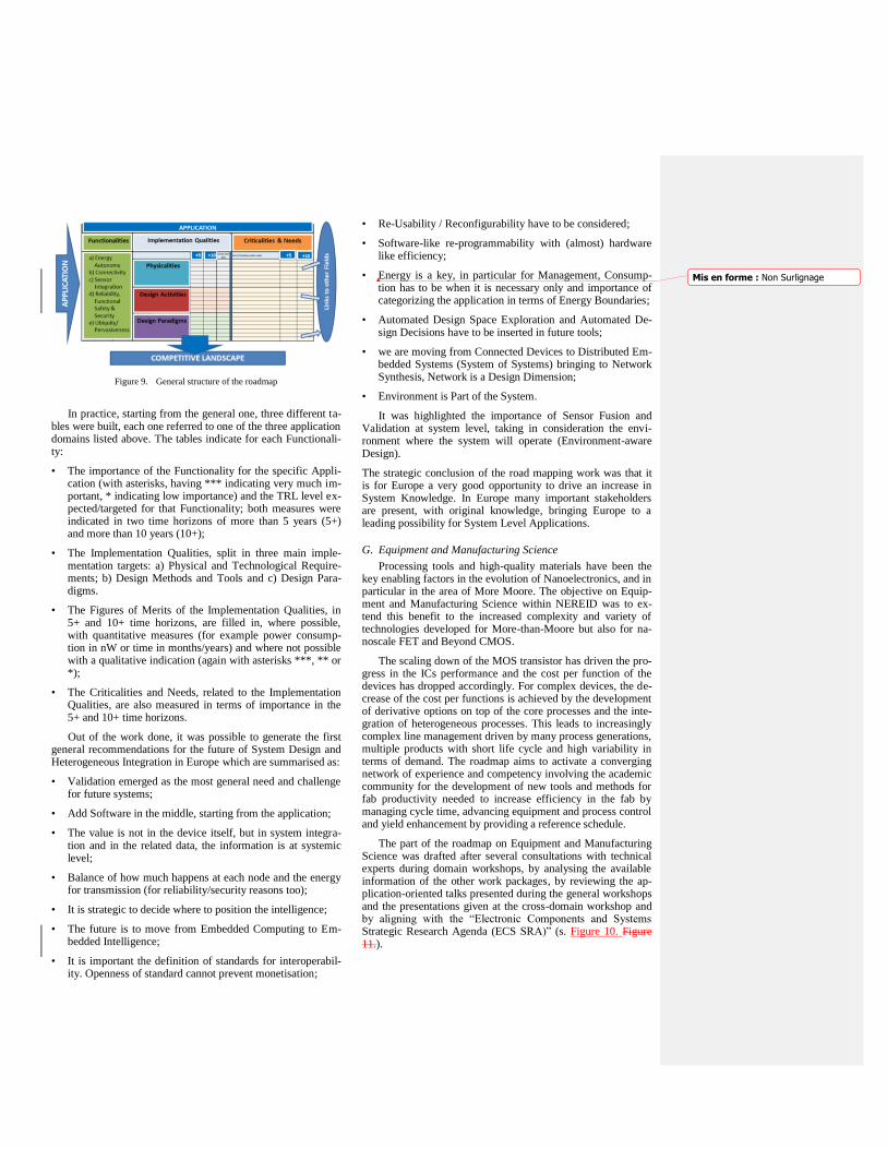
Figure 9. General structure of the roadmap
In practice, starting from the general one, three different ta-bles were built, each one referred to one of the three application domains listed above. The tables indicate for each Functionali-ty:
• The importance of the Functionality for the specific Appli-cation (with asterisks, having *** indicating very much im-portant, * indicating low importance) and the TRL level ex-pected/targeted for that Functionality; both measures were indicated in two time horizons of more than 5 years (5+) and more than 10 years (10+);
• The Implementation Qualities, split in three main imple-mentation targets: a) Physical and Technological Require-ments; b) Design Methods and Tools and c) Design Para-digms.
• The Figures of Merits of the Implementation Qualities, in 5+ and 10+ time horizons, are filled in, where possible, with quantitative measures (for example power consump-tion in nW or time in months/years) and where not possible with a qualitative indication (again with asterisks ***, ** or *);
• The Criticalities and Needs, related to the Implementation Qualities, are also measured in terms of importance in the 5+ and 10+ time horizons.
Out of the work done, it was possible to generate the first general recommendations for the future of System Design and Heterogeneous Integration in Europe which are summarised as:
• Validation emerged as the most general need and challenge for future systems;
• Add Software in the middle, starting from the application;
• The value is not in the device itself, but in system integra-tion and in the related data, the information is at systemic level;
• Balance of how much happens at each node and the energy for transmission (for reliability/security reasons too);
• It is strategic to decide where to position the intelligence;
• The future is to move from Embedded Computing to Em-bedded Intelligence;
• It is important the definition of standards for interoperabil-ity. Openness of standard cannot prevent monetisation;
• Re-Usability / Reconfigurability have to be considered;
• Software-like re-programmability with (almost) hardware like efficiency;
• Energy is a key, in particular for Management, Consump-tion has to be when it is necessary only and importance of categorizing the application in terms of Energy Boundaries;
• Automated Design Space Exploration and Automated De-sign Decisions have to be inserted in future tools;
• we are moving from Connected Devices to Distributed Em-bedded Systems (System of Systems) bringing to Network Synthesis, Network is a Design Dimension;
• Environment is Part of the System.
It was highlighted the importance of Sensor Fusion and Validation at system level, taking in consideration the envi-ronment where the system will operate (Environment-aware Design).
The strategic conclusion of the road mapping work was that it is for Europe a very good opportunity to drive an increase in System Knowledge. In Europe many important stakeholders are present, with original knowledge, bringing Europe to a leading possibility for System Level Applications.
G. Equipment and Manufacturing Science
Processing tools and high-quality materials have been the key enabling factors in the evolution of Nanoelectronics, and in particular in the area of More Moore. The objective on Equip-ment and Manufacturing Science within NEREID was to ex-tend this benefit to the increased complexity and variety of technologies developed for More-than-Moore but also for na-noscale FET and Beyond CMOS.
The scaling down of the MOS transistor has driven the pro-gress in the ICs performance and the cost per function of the devices has dropped accordingly. For complex devices, the de-crease of the cost per functions is achieved by the development of derivative options on top of the core processes and the inte-gration of heterogeneous processes. This leads to increasingly complex line management driven by many process generations, multiple products with short life cycle and high variability in terms of demand. The roadmap aims to activate a converging network of experience and competency involving the academic community for the development of new tools and methods for fab productivity needed to increase efficiency in the fab by managing cycle time, advancing equipment and process control and yield enhancement by providing a reference schedule.
The part of the roadmap on Equipment and Manufacturing Science was drafted after several consultations with technical experts during domain workshops, by analysing the available information of the other work packages, by reviewing the ap-plication-oriented talks presented during the general workshops and the presentations given at the cross-domain workshop and by aligning with the “Electronic Components and Systems Strategic Research Agenda (ECS SRA)” (s. Figure 10. Figure 11.).
Mis en forme : Non Surlignage
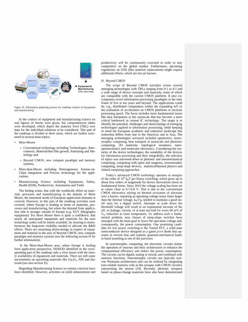
Figure 10. Information gathering process for roadmap creation on Equipmnet
and manufactuirng
In the context of equipment and manufacturing science no real figures of merits were given, but comprehensive tables were developed, which depict the maturity level (TRL) over time for the individual solutions to be considered. This part of the roadmap is divided in three areas, which are further struc-tured in several main topics:
• More Moore
o Conventional technology including Technologies, Inter-connects, Material/thin film growth, Patterning and Me-trology and
o Beyond CMOS, new compute paradigm and memory systems,
• More-than-Moore including Heterogeneous System-on-Chips integration and Process technology for the appli-cations,
• Manufacturing Science including Equipment, Safety, Health (ESH), Productivity, Automation and Yield.
The feeling exists, that with the worldwide effort on mate-rials, processes and manufacturing in the domain of More Moore, the imminent needs of European application domains is covered. However, in this part of the roadmap activities were covered, where Europe is leading in terms of materials, pro-cesses and manufacturing, but where the demand from applica-tion side is stronger outside of Europe (e.g. EUV lithography equipment). For More Moore there is quite a confidence, that nearly all anticipated equipment and materials for the next technology nodes will be timely available, by insuring to manu-facturers the long-term visibility needed to allocate the R&D efforts. There are remaining shortcomings in respect of equip-ment and material in the area of Beyond CMOS, new compute paradigm and memory systems (see the following section H for further information).
In the More-than-Moore area, where Europe is leading form application perspective, NEREID identified in the corre-sponding part of the roadmap only a view issues with the time-ly availability of equipment and materials. There are still some uncertainties on upcoming materials like Ga2O3, AlN and dia-mond (see also section D).
Regarding Manufacturing Science no serious concerns have been identified. However, activities on yield enhancement and
productivity will be continuously executed in order to stay competitive on the global market. Furthermore, upcoming regulations on ESH (like material replacement) might require additional efforts, which are not yet known.
H. Beyond CMOS
The scope of Beyond CMOS activities covers several emerging technologies with TRLs ranging from 0-1 to 4-5 and a wide range of device concepts and materials, some of which are compatible with the current CMOS platform. It also en-compasses novel information processing paradigms in the time frame of five to ten years and beyond. The applications could be, e.g., distributed computation within the expanding IoT or the realisation of accelerators on CMOS platforms to increase processing speed. The focus includes more fundamental issues like heat dissipation at the nanoscale that has become a most critical bottleneck in current IC technology. The target is to identify the potential, challenges and shortcomings of emerging technologies applied to information processing, while keeping in mind the European academic and industrial landscape that somewhat differs from that in the Americas and in Asia. The emerging technologies surveyed included spintronics, neuro-morphic computing, heat transport at nanoscale and phononic computing, 2D materials, topological insulators, nano-optomechanics and molecular electronics. Considering the ma-turity of the device technologies, the suitability of the devices for information processing and their integrability, the selection of topics was narrowed down to photonic and nanomechanical computing, computing with spins and magnons, neuromorphic computing, steep-slope devices, statistical/thermal physics and related computing approaches.
Today’s advanced CMOS technology operates at energies of the order of 10
4 kBT per binary switching, which gives up to
about four orders of magnitude for device innovations down to fundamental limits. Since 2010 the voltage scaling has been set at values close to 0.7-0.8 V. This is due to the conventional CMOS electronics relying on thermal excitation of electrons over a barrier, requiring an operating voltage many times larger than the thermal voltage, kBT/q, needed to maintain a good on-off ratio for a digital switch. Attempts to scale down the threshold voltage will result in an exponential increase of the off, or leakage, current, of at least ten-fold for every 60 mV of Vth reduction at room temperature. To address such a funda-mental problem, new classes of steep-slope switches have emerged with the main goal to lower the operation voltage and, consequently, the power consumption. One promising candi-date for low power switching is the Tunnel FET, a solid-state semiconductor device designed as a gated p-i-n diode that op-erates in reverse bias and exploits quantum-mechanical band-to-band tunneling at one of the junctions.
In neuromorphic computing, the electronic circuits mimic the operation of neurons and their architectures to enhance the computational efficiency and reduce the power consumption. The circuits can be digital, analog or mixed, and combined with memory functions. Neuromorphic circuits use typically non-von Neumann architectures and can be realized by integrating non-volatile memory cells as the synapse with CMOS circuitry representing the neuron [24]. Recently, photonic synapses based on phase-change materials have also been demonstrated
[25]. The circuits can include machine learning algorithms to perform, e.g., pattern recognition. Supervised learning is based on repetition of numerous samples, [26] and unsupervised learning needs a few presentations to master the function [27]
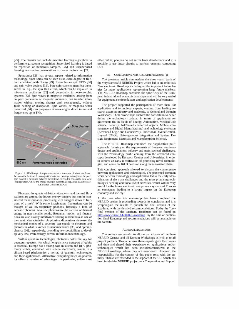
Spintronics [28] has several aspects related to information technology, since spins can be seen as an extra degree of free-dom combined with charge [29]. Examples are spin FETs [30] and spin valve devices [31]. Pure spin currents manifest them-selves in, e.g., the spin Hall effect, which can be exploited in microwave oscillators [32] and, potentially, in neuromorphic systems [33]. Spin waves in magnetic insulators, arising from coupled precession of magnetic moments, can transfer infor-mation without moving charges and, consequently, without Joule heating or dissipation. Spin waves, or magnons when quantized [34], can propagate at wavelengths down to nm and frequencies up to THz.
Figure 11. SEM image of a spin-valve device. A current of a few µA flows
between the first two ferromagnetic electrodes. Voltage arising from the pure
spin-current is measured between the last two electrodes. This is the non-local
configuration, where the charge and spin currents are separated (Courtesy of Dr. Marius Costache, ICN2).
Phonons, the quanta of lattice vibrations, and thermal fluc-tuations are among the lowest energy carriers that can be con-sidered for information processing with energies down to frac-tions of a meV. With some imagination, fluctuations can be thought of as low-frequency phonons, basically a kind of acoustic phonons. Acoustic phonons are the carriers of thermal energy in non-metallic solids. Brownian motion and fluctua-tions are also closely intertwined sharing randomness as one of their main characteristics. As physical dimensions decrease, the mechanical modes of a structure can couple to electrons and photons in what is known as nanomechanics [35] and optome-chanics [36], respectively, providing new possibilities to devel-op very low, even entropy-driven, information technology.
Within quantum technologies photonics holds the key for quantum repeaters, for which long-distance transport of qubits is essential. Europe has a strong base in silicon and III-V pho-tonics which, combined with silicon electronics, results in a silicon-based platform for a myriad of quantum technologies and their applications. Alternative computing based on photon-ics offers a number of advantages. In particular, unlike most
other qubits, photons do not suffer from decoherence and it is possible to use linear circuits to perform quantum computing [37].
III. CONCLUSIONS AND RECOMMENDATIONS (I)
The presented article summarizes the three years’ work of the very successful NEREID Project which led to an ambitious Nanoelectronic Roadmap including all the important technolo-gies for many applications representing large future markets. The NEREID Roadmap considers the specificity of the Euro-pean industrial and academic landscape and will be very useful for equipment, semiconductors and application developments.
The project supported the participation of more than 100 application and technology experts, coming from leading re-search actors in industry and academia, to General and Domain Workshops. These Workshops enabled the consortium to better define the technology roadmap in terms of application re-quirements (in the fields of Energy, Automotive, Medical/Life science, Security, IoT/Smart connected objects, Mobile con-vergence and Digital Manufacturing) and technology evolution (Advanced Logic and Connectivity, Functional Diversification, Beyond CMOS, Heterogeneous Integration and System De-sign, Equipment, Materials and Manufacturing Science).
The NEREID Roadmap combined the “application pull” approach, focusing on the requirements of European semicon-ductor and applications industry and main societal challenges, with the “technology push” coming from the advanced con-cepts developed by Research Centres and Universities, in order to achieve an early identification of promising novel technolo-gies, and cover the R&D needs all along the innovation chain.
This combined approach allowed to discuss the convergence between applications and technologies. The presented common work between technology and application led to the early iden-tification of the main challenges and the most promising tech-nologies needing additional R&D activities, which will be very useful for the future electronic components systems of Europe-an companies leading to a strong impact on the European economy and society.
At the time when this manuscript has been completed the NEREID project is proceeding towards its conclusion and it is wrapping-up the results to publish the final version of the Roadmap with the detailed recommendations. Today the “pre-final version of the NEREID Roadmap can be found on https://www.nereid-h2020.eu/roadmap. By the time of publica-tion final Roadmap and recommendations will be available on the website.
ACKNOWLEDGEMENTS
The authors are grateful to all the participants of the three NEREID General and all Domain Workshops as well as to all project partners. This is because these experts gave their views and time and shared their experience on applications and/or technologies which has been included/considered in the NEREID roadmap, where they are mentioned. However, the responsibility for the content of this paper rests with the au-thors. Thanks are extended to the support of the EU, which has been funded the NEREID project as a Cooperation and Support
action for three years from the European Union’s Horizon 2020 research and innovation programme under grant agreement No 685559.
REFERENCES
[1] F. Balestra, Nanoscale CMOS: Innovative Materials, Modeling and Characterization, Francis Balestra Ed., ISTE-Wiley (2010) ;
[2] F. Balestra, Beyond CMOS Nanodevices (tomes 1 et 2), Francis Balestra Ed., ISTE-Wiley (2014).
[3] ADAS (Advanced Driver Assistance System) by systems and sensors, Global Opportunity Analysis and Industry Forecast, 2013 – 2020, May 2015, (www.alliedmarketresearch.com).
[4] P. Gao, R. Hensley, A. Zielke, A road map to the future for the auto industry, McKinsey Quarterly October 2014
[5] European Roadmap Safe Road Transport, ERTRAC, June 2011 (www.ertrac.org).
[6] Report on Sensors for Wearable Electronics & Mobile Healthcare, Yole Development, 2015.
[7] Wearable Technology and the Internet of Things - Consumer views on wearables beyond health and wellness, An Ericsson Consumer Insight Summary Report, June 2016.
[8] S. C. Mukhopadhyay, Wearable Sensors for Human Activity Monitoring: A Review, IEEE Sensors Journal, Volume: 15, Issue: 3 , March 2015, pp. 1321 – 1330.
[9] P Abgrall and A-M Gué, Lab-on-chip technologies: making a microfluidic network and coupling it into a complete microsystem—a review, Journal of Micromechanics and Microengineering, Volume 17, Number 5, 2007, pp. R15-R49.
[10] D. Huh, G.A. Hamilton, D. E. Ingber. From 3D cell culture to organs-on-chips, Trends in Cell Biology. Volume 21, Issue 12, December 2011, pp. 745-754
[11] S Boisseau, G Despesse, T Ricart, E Defay and A Sylvestre Published 31 August 2011 • IOP Publishing Ltd , Smart Materials and Structures, Volume 20, Number 10
[12] Larcher, L., Roy, S., Mallick, D., Podder, P., de Vittorio, M., Todaro, T., Guido, F., Bertacchini, A., Hinchet, R., Keraudy, J. and Ardila, G. (2014) Vibrational Energy Harvesting, in Beyond-CMOS Nanodevices 1 (ed F. Balestra), John Wiley & Sons, Inc., Hoboken, NJ, USA. doi: 10.1002/9781118984772.ch6)
[13] A. Khaligh, P. Zeng, C. Zheng, Kinetic Energy Harvesting Using Piezoelectric and Electromagnetic Technologies—State of the Art, IEEE Trans. Indus. Elec., 57(3): 850-860 (2010)
[14] Puscasu, O., Monfray, S., Savelli, G., Maitre, C., Pemeant, J. P., Coronel & Guyomar, D. (2012, December). An innovative heat harvesting technology (HEATec) for above-Seebeck performance. In Electron Devices Meeting (IEDM), 2012 IEEE International (pp. 12-5). IEEE.
[15] International Technology Roadmap for Photovoltaic (ITRPV) 2017
[16] N.Borges Carvalho et al., "Wireless Power Transmission: R&D Activities Within Europe," in IEEE Transactions on Microwave Theory and Techniques, vol. 62, no. 4, pp. 1031-1045, April 2014. doi: 10.1109/TMTT.2014.2303420
[17] J.F. Rohan, M. Hasan, S. Patil, D. Casey and T. Clancy, Chapter 6 – Energy storage materials and architectures at the nanoscale, in ICT-Energy - Nanoscale energy management concepts towards Zero-Power Information and Communication Technology / (2014) Editors, G. Fagas, L. Gammaitoni, D. Paul and G. Abadal Berini, Intech Publications, Croatia. pp 107-138, ISBN 980-953-307-1005-8, DOI: 10.5772/57139
[18] R. Ulrich and L. Schaper, “Materials options for dielectrics in integrated capacitors,” in Proc. Int. Symp. Adv. Packag. Mater., Process., Properties Inter., 2000, pp. 38–43
[19] A. Romani et al., IEEE Computer 2017
[20] International Technology Roadmap for Semiconductors, Design, 2007 Edition
[21] International Technology Roadmap for Semiconductors, Design, 2009 Edition
[22] International Technology Roadmap for Semiconductors, Design, 2011 Edition
[23] M. Crepaldi, M. C. Grosso, A. Sassone, S. Gallinaro, S. Rinaudo, M. Poncino, E. Macii, D. Demarchi, “A Top-Down Constraint-Driven Methodology for Smart System Design,” IEEE Circuits Syst. Mag., vol. 14, no. 1, pp. 37–57, 2014
[24] G. W. Burr et al., Neuromorphic computing using non-volatile memory, Advances in Physics: X 2 (2017) 89.
[25] Z. Cheng et al., On-chip phase-change photonic memory and computing, Proc. SPIE 10345 (2017) 1034519.
[26] M. Schmuker, T. Pfeil, and M. P. Nawrot, A neuromorphic network for generic multivariate data classification, PNAS 111 (2014) 2018.
[27] T. Masquelier, R. Guyonneau and S.J. Thorpe, Spike Timing Dependent Plasticity Finds the Start of Repeating Patterns in Continuous Spike Trains, PLoS One 3 (2008) e1377.
[28] I. Zutic, J. Fabian, and S. Das Sarma, Spintronics: Fundamentals and applications, Rev. Mod. Phys. 76 (2004) 323.
[29] S. A. Wolf et al., Spintronics: A Spin-Based Electronics Vision for the Future, Science 294 (2001) 1488.
[30] S. Datta and B. Das, Electronic analogue of the electro-optlc modulator, Appl. Phys. Lett. 56 (1990) 665.
[31] R. Jansen, The spin-valve transistor: a review and outlook, J. Phys. D: Appl. Phys. 36 (2003) R289.
[32] T. Chen et al., Spin-Torque and Spin-Hall Nano-Oscillators, Proc. IEEE 104 (2016) 1919.
[33] J. Torrejon et al., Neuromorphic computing with nanoscale spintronic oscillators, Nature 547 (2017) 428.
[34] S. Neusser and D. Grundler, Magnonics: Spin Waves on the Nanoscale, Adv. Mater. 21 (2009) 2927.
[35] A.N. Cleland, Foundations of Nanomechanics (Springer-Verlag, Berlin, Heidelberg, New York, 2003).
[36] M. Aspelmayer, T. Kippenberg and F. Marquardt, Cavity Optomechanics, Rev. Mod. Phys. 86 (2014) 1391.
[37] See, for example, J. Belhassen et al., On-chip III-V monolithic integration of heralded single photon sources and beam splitters, Appl. Phys. Lett. 112 (2018) 071105.