nanoscale investigation of polarization interaction and
TRANSCRIPT

University of Nebraska - LincolnDigitalCommons@University of Nebraska - LincolnTheses, Dissertations, and Student Research:Department of Physics and Astronomy Physics and Astronomy, Department of
January 2008
Nanoscale Investigation of Polarization Interactionand Polarization Switching in Ferroelectric P(VDF-TrFE) Copolymer SamplesJihee KimUniversity of Nebraska at Lincoln, [email protected]
Follow this and additional works at: http://digitalcommons.unl.edu/physicsdiss
Part of the Physics Commons
This Article is brought to you for free and open access by the Physics and Astronomy, Department of at DigitalCommons@University of Nebraska -Lincoln. It has been accepted for inclusion in Theses, Dissertations, and Student Research: Department of Physics and Astronomy by an authorizedadministrator of DigitalCommons@University of Nebraska - Lincoln.
Kim, Jihee, "Nanoscale Investigation of Polarization Interaction and Polarization Switching in Ferroelectric P(VDF-TrFE) CopolymerSamples" (2008). Theses, Dissertations, and Student Research: Department of Physics and Astronomy. 4.http://digitalcommons.unl.edu/physicsdiss/4
NANOSCALE INVESTIGATION OF
POLARIZATION INTERACTION AND POLARIZATION SWITCHING IN
FERROELECTRIC P(VDF-TrFE) COPOLYMER SAMPLES
by
Jihee Kim
A DISSERTATION
Presented to the Faculty of
The Graduate College at the University of Nebraska
In Partial Fulfillment of Requirements
For the Degree of Doctor of Philosophy
Major: Physics and Astronomy
Under the Supervision of Professor Stephen Ducharme
Lincoln, Nebraska
May, 2008

NANOSCALE INVESTIGATION OF
POLARIZATION INTERACTION AND POLARIZATION SWITCHING IN
FERROELECTRIC P(VDF-TrFE) COPOLYMER SAMPLES
Jihee Kim, Ph. D.
University of Nebraska, 2008
Adviser: Stephen Ducharme
Ferroelectric properties of thin films and self-assembly of copolymers of
polyvinylidene fluoride with trifluoroethylene (P(VDF-TrFE) have been studied. All
samples were fabricated with Langmuir-Blodegtt (LB) film deposition technique. Two
main observations are presented in this dissertation. One is a polarization interaction
effect in multi-layered thin films made of two different copolymers, and the other is local
polarization switching of the self-assembly, called nanomesas.
The multilayer films were built with two different content ratio of P(VDF-TrFE)
copolymers. They were P(VDF-TrFE 80:20) and P(VDF-TrFE 50:50) with phase
transition temperatures of 133 ± 4 ºC and 70 ± 4 ºC respectively. The polarization
interaction effect resulted in transition temperature changes of the materials, and the
determined interaction length was approximately 11 nm, perpendicular to the film plane.
Nanomesas of P(VDF-TrFE) copolymer were found during annealing study of
thinner films with less than 3 deposited layer thin films. Nanomesas are disk shaped
isolated islands approximately 9 nm in height and 100 nm in diameter in average.
Ferroelectric switching properties of nanomesas have been shown macroscopically in the
previous studies. In this work, the switching properties of individual nanomesas were
probed at nanoscale. Nanomesas, switched with ± 7 Vdc were recorded using
piezoresponse force microscopy (PFM). Switching hysteresis loops from a local area of
12~15 nm2 within an individual nanomesa were also obtained using switching
spectroscopy PFM (SS-PFM). The coercive field determined from the well behaved
switching loops is ~250 ~ 450 MV/cm.

iv
This is dedicated to Jesus
Through Mary,

v
Acknowledgements
First of all I would like to express my deep appreciation to my advisor, Prof.
Stephen Ducharme for his guidance through my years as his graduate student. With his
guidance I made it this far, and his enthusiasm for science and his optimistic attitude have
been a great inspiration for me.
I would like to thank Prof. Shireen Adenwalla for her sincere concern, care, and
understanding during my troubled times as well as for being a committee member. Also, I
would like to thank Prof. Evgeny Tsymbal and JiangYu Li for allowing me to have them
as my dissertation committee and helping me to improve this dissertation. Also, I would
like to express my appreciation to Prof. Vladimir Fridkin for his encouragement, and Prof.
Sitaram Jaswal for being my family away from home, and Prof. Paul Finkler for his
attentive and cheerful messages on occasion.
I would like to thank Dr. Hoydoo You and Dr. Adreas Menzel for their
instructions on using the Advanced Photon Source at Argonne National Laboratory and
their helpful suggestions for analysis. Also, I would like to thank Dr. Sergei Kalinin, Dr.
Brian Rodriguez, Dr. Stephen Jesse, and Dr. Arthur Baddorf for their kind instructions on
PFM and SS-PFM system and generosity in sharing the equipment while I was working
at the center for Nanophase Materials Sciences at Oak Ridge National Laboratory. I am
also grateful to Dr. Lan Gao for providing me help and support outside of lab during my
visit at Oak Ridge.

vi
I would like to thank Dr. Lu in the Electrical Engineering Department at UNL and
his group members, Dr. Jing Shi, Hao Wang, and many others for their support with the
Scanning Tunneling Microscopy system and the Laser assisted self-assembly
nanoimprint system. I would like to thank Brian Jones and Dr. Lanping Yue for their
instruction and kind help for using X-ray system and Atomic Force Microscopy system,
respectively.
Now, I would like to thank all my former and current group members who have
been great a help in many ways in the lab and discussion. I am thankful to Dr. Alexander
Sorokin for his instruction on the Langmuir-Blodgett technique, Dr. Mengjun Bai for his
innovative initial work on nanomesas, Dr. Christina Othon for helping me with many
things in the lab in addition to her great friendship, and Dr. Matt Poulsen for helping me
with trouble shooting the lab equipment and discussions on X-ray study. I would like to
also thank Dr. Timothy Reece and Kristin Kraemer for their support at the last moment of
my Ph.D program.
I would like to give my special thanks to my friends Dr. Snow Balaz, Dr. Jeong
Park, Dr. Luis Rosa and his wife, Francis, and Shannon Fritz and Mark Stigge for their
great friendship and love they bear for me. Also, I am very grateful to Fr. Christopher
Barak, Fr. Daniel Seiker, the Pink sisters in Lincoln, Suki Smith, Helena Jang, Jin Kim,
and Sangwon Kim for their payers and wishes for me to complete my dissertation.

vii
Last but not least, I would like to thank my family. My Mom and Dad are the core
of everything that I have accomplished. Without their love, care, support, and prayers
nothing would have happened. Also, I am deeply thankful to my sisters, Jihyun and Jisun,
and their families for their great support. There is nothing better than the friendship that
comes from sisters in life. Above all, I give all my thanks, mentioned here and remained
in my heart unexpressed to my heavenly mother and father for their glory.

viii
TABLE OF CONTENTS
Abstract------------------------------------------------------------------------------------------------ii
Dedication--------------------------------------------------------------------------------------------iv
Acknowledgements----------------------------------------------------------------------------------v
Table of Contents----------------------------------------------------------------------------------viii
Chapter 1 Introduction-----------------------------------------------------------------------------1
1.1 Ferroelectricity-------------------------------------------------------------------------3
1.2 Ferroelectric polymer: P(VDF-TrFE) copolymers------------------------------14
1.3 Langmuir-Blodgett (LB) thin films of P(VDF-TrFE) copolymers------------19
Chapter 2 Sample Characterization-------------------------------------------------------------24
2.1 Thin Films----------------------------------------------------------------------------25
2.2 Self –assembly Structure: Nanomesas--------------------------------------------29
2.3 Capacitors-----------------------------------------------------------------------------33
2.4 Thickness of P(VDF-TrFE) Thin Films------------------------------------------38
2.4.1 Introduction---------------------------------------------------------------38
2.4.2 Measurements-------------------------------------------------------------40
2.4.3 Results---------------------------------------------------------------------46
2.5 Real-time Observation of Nanomesa Formation--------------------------------54
2.5.1 Measurements-------------------------------------------------------------54
2.5.2 Results---------------------------------------------------------------------55
Chapter 3 Polarization Interaction in Multilayered Thin Films of P(VDF-TrFE)--------65

ix
3.1 Introduction---------------------------------------------------------------------------65
3.2 Sample Preparation------------------------------------------------------------------69
3.3 Experimental Method---------------------------------------------------------------73
3.4 Results and Discussion--------------------------------------------------------------81
3.5 Conclusions---------------------------------------------------------------------------99
Chapter 4 Polarization Switching of Nanomesas--------------------------------------------106
4.1 Introduction ------- -----------------------------------------------------------------106
4.2 Sample Preparation----------------------------------------------------------------109
4.3 Polarization Switching Observation 1 with PFM------------------------------111
4.3.1 Principles of PFM Scanning-------------------------------------------111
4.3.2 Scanning Conditions and Issues in PFM-----------------------------115
4.3.3 PFM Results and Discussion------------------------------------------118
4.4 Polarization Switching Observation 2 with SS-PFM--------------------------127
4.4.1 Principles of SS-PFM Scanning---------------------------------------127
4.4.2 Scanning Conditions and Issues in SS-PFM------------------------131
4.4.3 SS-PFM Results and Discussion--------------------------------------133
4.5 Conclusion--------------------------------------------------------------------------142
Appendices-----------------------------------------------------------------------------------------145
Appendix A. Initial Work for Near Field PSM---------------------------------------145
Appendix B. Nanoimprints on P(VDF-TrFE 70:30) Copolymer Films-----------159

Chapter 1 Introduction
1
Chapter 1 Introduction
Ferroelectric copolymers of vinylidene fluoride (VDF)x with trifluoroethylene
(TrFE)100-x have been a main subject in our research group for the last decade. P(VDF-
TrFE) is a very well known ferroelectric copolymer. The development of P(VDF-TrFE)
copolymer is originated from discovery of the piezoelectricity and pyroelectricity of
PVDF. The piezoelectricity and the pyroelectricity of PVDF were first discovered in
1969 and 1971, respectively.1,2 Since then, PVDF was widely investigated to understand
its basic properties as well as for its technical applications, such as electromechanical
transducers, pyroelectric detectors for infrared imaging, etc. Due to the potential
inexpensive massive fabrication, which is a merit of flexible polymers, PVDF had drawn
much research interests to it. As one way to improve the piezoelectricity and
pyroelectricity of PVDF, copolymers of PVDF were also synthesized 3 and investigated.
P(VDF-TrFE) is one of those synthesized copolymers for that purpose. Eventually, in the
early 1980’s ferroelectricity of both PVDF and P(VDF-TrFE) were clearly revealed.4,5
The more detailed development of PVDF is well introduced in the specialized text by
Wang et al.6,7
Mostly, ferroelectric polymers have been studied in a form of thin films. Thin
films can be fabricated in many different ways, for example, solution casting, dipping or
spinning.8 In our lab, we have prepared thin films of P(VDF-TrFE) copolymer by using
Langmuir-Blodgett technique.9 Thin films of P(VDF-TrFE) made by Langmuir-Blodgett

Chapter 1 Introduction
2
technique show very good ordering, which results in strong X-ray diffraction peak, which
are discussed in later chapters(see section 2.2, and chapter3). The representative
copolymers of 70% VDF with 30% of TrFE, P(VDF-TrFE 70:30), have been intensively
studied in our group.10 In addition to the fundamental characterization studies (crystal
structure, dielectric properties, switching properties of thin films of P(VDF-TrFE)), many
application studies (developing memory devices, pyroelectric scanning microscope,
nanofabrication) also have been done.
There are two main projects presented in this dissertation. One is the polarization
interaction between P(VDF-TrFE 80:20) and P(VDF-TrFE 50:50) copolymers presented
in Chapter 3, and the other one is the polarization switching in a self-assembly films of
P(VDF-TrFE 70:30) copolymer, namely nanomesas, presented in Chapter 4. Nanomesas
are disk-shaped islands with dimensions of approximately 9 nm in thickness and 100 nm
in diameter, and they will be introduced in the next chapter 2. There are two appendices
at the end of the dissertation. In appendix A, an initial testing work for setting a Near
Field Pyroelectric Scanning Microscopy (NFPSM) system is summarized. In appendix B,
Nan imprints attempts are summarized.
In this chapter, before presenting all the works mentioned above, basic concepts
of ferroelectricity, and introduction of P(VDF-TrFE) copolymers, and Langmuir-Blodgett
thin film fabrication technique will be briefly introduced. The basic diagnostic sample
characterization measurements taken routinely in our lab will be introduced in chapter 2.

Chapter 1 Introduction
3
1.1 Ferroelectricity
A ferroelectric material exhibits a stable macroscopic polarization that can be
repeatably switched by an external electric field between equal-energy states of opposite
polarization.10 Dielectric materials can be categorized as nonferroelectric (normal
dielectric or paraelectric) and ferroelectric11. In paraelectric (normal dielectric) materials,
electric polarization occurs when an electric field is applied to the materials. There are
three different types of electric polarization according to the mechanisms of electric
polarization; Electronic polarization, atomic or ionic polarization, and orientational
polarization. Electronic polarization occurs due to the displacement of the outer electron
clouds with respect to the inner positive atomic cores under an applied field. In the case
of atomic or ionic polarization, the electric field displaces atoms or ions of a polyatomic
molecule relative to each other. Orientational polarization occurs among the materials
consisting of molecules or particles with a permanent dipole moment. To have permanent
dipole moments, the material should be composed of molecules with an asymmetrical
structure in which the centroid of the negative charge and that of the positive charge are
not coincident. 11 The permanent dipole moments are randomly oriented in their
equilibrium states of in paraelectric material; however, under the influence of an electric
field they become aligned to the direction of the field, and then show macroscopic
electric polarization. When the field is removed, the electric polarizations of paraelectric
materials return to their non-polarized equilibrium state.
Chapter 1 Introduction
4
Ferroelectric materials have the electric polarization in their equilibrium states
without help of an external electric field. This type of polarization is called the
spontaneous polarization. Spontaneous polarization can be described as ordered
orientational polarization in the absence of applied field, also spontaneous polarization is
reversible. To have ordered polarization, the ferroelectric material should be crystalline.
This implies that the crystal structure and dielectric properties of ferroelectric materials
are interrelated. This state of spontaneous polarization is also temperature dependant.
Roughly speaking, above the critical temperature, called the phase transition temperature,
Tc, the spontaneous polarization disappears. In other word, at this Tc ferroelectric
materials undergo phase transition from the ordered phase, ferroelectric, to disordered
phase, paraelectric as temperature increases, and vice versa when temperature decreases.
In the remainder of this chapter, we will look at the dielectric phase transition of
ferroelectric materials described by Landau-Ginzburg-Devonshire (LGD) thermodynamic
free energy model developed from the Landau theory of continuous phase transitions, and
also look at the reversibility of the spontaneous polarization with respect to the applied
field in a typical ferroelectric hysteresis loop.12,13,14
Phase Transition10,11
The Landau theory of continuous phase transitions is based on a thermodynamic
free energy, which can be expressed as a power series in a small quantity called the order
parameter. Ginzburg developed Mean-field models of the continuous ferroelectric phase
transition, 15,16,17 which treat the polarization as an order parameter in the Landau theory.

Chapter 1 Introduction
5
A similar treatment was developed by Devonshire shortly thereafter. 18 , 19 , 20 For this
dissertation LGD formalism for the uniaxial case, where the electric polarization and an
applied field are parallel to the unique crystalline axis, shall only be discussed.
The LGD form of the Gibbs free-energy density can be written15,16
PEPPPG −+++= 6420 642
β γα (1) G
where E is the electric field, G0 is the free-energy density of the paraelectric phase at zero
field, and the expansion coefficients α, β, and γ are in general dependent on temperature
and pressure. The equilibrium condition corresponds to the absolute minimum of the
free-energy density. The Landau theory requires that the first coefficient α vanish at the
so-called Curie temperature T , so that the simplest form for the first coefficient is 0
)(10
0
TTC
−=ε
α
(2)
where T is the temperature, C >0 is the Curie-Weiss constant, and ε0 is the permittivity of
free space. The coefficients C, β, and γ are generally assumed independent of temperature,
but it is often best to confine the LGD analysis to temperatures near the Curie
temperature to ensure this. The sign of the second coefficient β determines whether the
transition is first-order (β<0) or second-order (β >0).
The constitutive relation between polarization P and electric field E is obtained
from the minimum of the free energy Eq.1, yielding the expression.
(3) 53 PPPE γβα ++=

Chapter 1 Introduction
6
If the electric field is not high, we can use first-order approximation for paraelectric
phase where P is small, then we have
PTE )00
−= α TC
P (1=ε
(4)
P for T can be expressed as combined with the definition ofα , Eq.2. cT⟩
EP 0χε= (5)
Thus, from Eq. 4 and Eq. 5 the inverse polarizability in the paraelectric phase.
( ) )(1 0
0 cTTC
TTPE
⟩−
=∂∂= ε
χ (6)
This is the so-called Curie-Weiss law, which is built into the definition of α. The total
dielectric constant of the medium ε ε χ+= ∞
0TC =
0=P
contains contributions ε∞ from the
background electronic polarizability.
The second-order LGD ferroelectric is described by the free energy density in Eq.1 with
expansion coefficient values C > 0, β > 0, and γ = 0. The second-order LGD ferroelectric
has two distinct phases, a nonpolar paraelectric phase and a polar ferroelectric phase. The
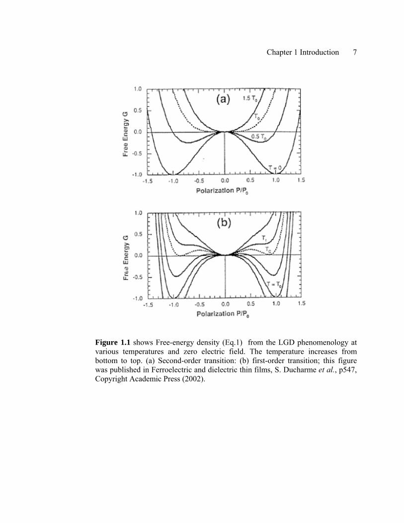
free-energy plots in Figure 1a illustrate the distinction between these phases. At
temperatures above the equilibrium phase transition temperatureT , the free energy
has a single minimum free energy at . This is the paraelectric phase, which has no
spontaneous polarization at zero applied electric field.
Chapter 1 Introduction
7
Figure 1.1 shows Free-energy density (Eq.1) from the LGD phenomenology at various temperatures and zero electric field. The temperature increases from bottom to top. (a) Second-order transition: (b) first-order transition; this figure was published in Ferroelectric and dielectric thin films, S. Ducharme et al., p547, Copyright Academic Press (2002).

Chapter 1 Introduction
8
CAt temperatures below T in zero field, there are two equivalent minimum free energy,
where the magnitude of the equilibrium polarization in zero electric field, the
spontaneous polarization is
( ) )(||
0CS TT
CT
P ⟨=±=βεβ
α
0=
SPEP ±== )0(
0T − (7)
which is obtained by solving Eq. 3 when E , and by ignore the 5th power term
(remember β > 0 here). The zero-field equilibrium polarization can point
in either direction along the symmetry axis, corresponding to the two energetically
equivalent states of the ferroelectric crystal at zero electric field. The spontaneous
polarization in the ferroelectric phase decreases steadily with increased temperature and
vanishes at the transition temperature, as shown in Figure 2a. At a second-order phase
transition, the order parameter (spontaneous polarization) decreases smoothly to zero.
The first-order LGD ferroelectric is described by the free energy density in Eq.1
with expansion coefficient values 0⟨β and 0⟩γ . The first-order transition is more
complicated than the second-order transition. The representative characteristics of the
first-order transition are firstly the discontinuous transition at the Curie temperature ,
and secondly the actual phase transition is not the same as , and thirdly there is a
region of metastable phase coexistence. We can calculate T the temperature above
which there is no more ferroelectric phase. These characteristic temperatures T , , and
are manifest in thermal hysteresis of first-order transition materials.
0T
CT 0T
1
0 CT
1T

Chapter 1 Introduction
9
Figure 1.2 shows spontaneous polarization from the mean-field ferroelectric models: (a) the second-order LGD ferroelectric from Eq. 7 (solid Line) and the second order mean-field Ising model (dashed line); (b) the first-order LGD ferroelectric, where the solid lines denote equilibrium solutions and the dashed lines denote metastable solutions; this figure was published in Ferroelectric and dielectric thin films, S. Ducharme et al., p548, Copyright Academic Press (2002).

Chapter 1 Introduction
10
The free-energy plots of the first-order LGD ferroelectric is shown in Figure 1b.
For the minimum values of G for this is
0=dPdG α || 53 =+− PPP γβ (8)
and the solution of Eq.8 yields and 0=SP
[ ]2
/1
2/12 )4|(|||21
⎭⎬⎫
⎩⎨⎧ −±±= γαββ
γS
0=
P (9)
Eq.9 shows that whenα ( , , and this implies that changes
discontinuously from or to abruptly at ,
this is the nonequilibrium case, and this is the distinctive characteristic of the first order
phase transition. Now let us look at the actual transition temperature T , this is the
equilibrium case, which is higher than the Curie temperature T . The T can be
calculated by imposing the condition that the free energy of the polar and the nonpolar
phases are equal atT . This leads Eq.1 to
)0TT = 2/1)/|(| γβ±=P
2/1)/|(| γβ+=SP 2/1)/|(| γβ−=SP P
C
0 C
C
SP
0= 0TT =
061||
41)(
21 642
0
0 =+−−
PPPCTTC γβ
ε (10)
And, the applied field is set equal to zero. This gives
0||)( 53
0
0 =+−−
== PPPCTT
dPdGE C γβ
ε (11)
From Eq. 10 and 11, we obtain

Chapter 1 Introduction 11
2/1||
43
⎥⎦
⎤⎟⎟⎠
⎞⎜⎜⎝
⎛γβ
⎢⎣
⎡±=SP (12)
γ
βε2
00||
163 CTTC =−
γβε /)16/3 20C
(13)
This results show that the discrepancy between the actual phase transition temperature
and the Curie temperature is ( , and the magnitude of the discontinuous
change in spontaneous polarization is γβ 4/||3 . Lastly, can be calculated by
applying the minimum free-energy condition that only one value of P above ,
corresponding to the condition
1T
1T
04||0
012 =−
−CTT
εγβ (14)
thus
γβε 2
001 4
1 CTT +=
C 0
0=
CT 1
(15)
Figure 2.b summarizes the thermal hysteresis. It shows that if a crystal is not in
equilibrium, the paraelectric phase can persist on cooling through T as far as T due to
the local minimum at P , and the ferroelectric phase can persist on heating through
as far as T due to the local minima at . SP±
Dielectric Anomaly11
)/( 0TTC −=The Curie-Weiss law, ε in paraelectric phase from Eq.6 with
ignoring the background electronic polarizability predicts anomalous behavior of the

Chapter 1 Introduction 12
dielectric constant near the Curie temperature. In fact, the dielectric constants of
ferroelectric materials show very rapid increases around the phase transition and result in
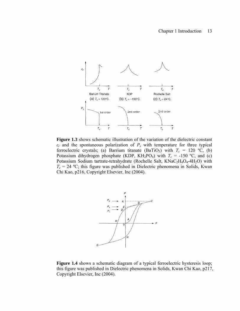
a high peak. Therefore, the high peak of the dielectric constants is used to determine the
phase transition temperatures of the materials (see Figure 3)
Ferroelectric Hysteresis loop11
The most prominent features of ferroelectric properties are hysteresis and
nonlinearity in the relation between the polarization P and the applied electric field E .
A typical hysteresis loop is shown schematically in Figure 4. When the field is small, the
polarization increases linearly with the field. This is due mainly to field-induced
polarization because the field is not large enough to cause orientation of the domains
(portion 0A). At fields higher than the low-field range, polarization increases nonlinearly
with increasing field because all domains start to orient toward the direction of the field
(portion AB). At high fields, polarization will reach a state of saturation corresponding to
portion BC, in which most domains are aligned toward the direction of the poling field.
Now, if the field is gradually decreased to zero, the polarization will decrease, following
the path CBD. By extrapolating the linear portion CB to the polarization axis (or zero-
field axis) at E, 0E represents the spontaneous polarization P and 0D represents the
remanent polarization P . The linear increase in polarization from P to is due
mainly to the normal field-induced dielectric polarization. is smaller than P because
when the field is reduced to zero, some domains may return to their original position.
S
r S pP
rP S
Chapter 1 Introduction 13
Figure 1.3 shows schematic illustration of the variation of the dielectric constant εr and the spontaneous polarization of Ps with temperature for three typical ferroelectric crystals; (a) Barrium titanate (BaTiO3) with Tc = 120 ºC, (b) Potassium dihydrogen phosphate (KDP, KH2PO4) with Tc = -150 ºC, and (c) Potassium Sodium tartrate-tetrahydrate (Rochelle Salt, KNaC2H4O4-4H2O) with Tc = 24 ºC; this figure was published in Dielectric phenomena in Solids, Kwan Chi Kao, p216, Copyright Elsevier, Inc (2004).
Figure 1.4 shows a schematic diagram of a typical ferroelectric hysteresis loop; this figure was published in Dielectric phenomena in Solids, Kwan Chi Kao, p217, Copyright Elsevier, Inc (2004).

Chapter 1 Introduction 14
For most ferroelectric materials, the component due to the normal field-induced
dielectric polarization is very small compared to the spontaneous polarization; therefore,
for most application, this component can be ignored and the saturation region is nearly
flat in practice. The magnitude of the difference between and in Figure 4 is
exaggerated for the purpose of clear illustration. The field required to bring the
polarization to zero is called the coercive field (portion 0R on zero polarization axis).
The hysteresis arises from the energy needed to reverse the metastable dipoles during
each cycle of the applied field. The area of the loop represents the energy dissipated
inside the specimen as heat during each cycle.
pP SP
CE
1.2 Ferroelectric Polymer: PVDF and P(VDF-TrFE)
Now, let us look at origin of the ferroelectricity of PVDF polymer, and its crystal
structure and difference between PVDF and its copolymer with trifluoroethylene (TrFE),
P(VDF-TrFE).
Molecular and Crystal Structure of PVDF
The vinylidene fluoride C2H2F2 monomers form a linear carbon-carbon chain with
structure −(CH2−CF2 )−. The monomer has a dipole moment pointing roughly from the
fluorines to the hydrogens. In the polymer chains (CH2−CF2 )n, the monomers arrange in
a fashion to minimize the potential energy of the chains. There are two most common
stable conformations. One is the all-trans TTTT conformation (see Figure 5.a), and the
other is the alternating trans-gauche GTGT conformation (see Figure 5.b). The trans

Chapter 1 Introduction 15
bond (T ) has a dihedral angle of approximately ~180 º and the left and right gauche
bonds (G and G ) have dihedral angles of approximately ± 60 º. The all-trans TTTT
conformation has a net dipole moment of about 7.0 × 10⁻³⁰ C-m essentially perpendicular
to the chain axis21 and the alternating trans-gauche GTGT conformation has 4.0 × 10⁻³⁰
C-m and 3.4 × 10⁻³⁰ C-m in perpendicular and in parallel to the chain respectively due to
the inclination of dipoles to the molecular axis22.
Crystal structure of the all-trans (TTTT ) conformation is called β phase, and it is
ferroelectric phase. β phase is orthorhombic m2m structure with the chains along the
crystal c-axis and the dipoles aligned approximately along the crystal b-axis as shown in
Figure 5c.3,23 ,24 , 25 This β phase is a uniaxial ferroelectric, as the polarization can be
repeatably switched between opposite but energetically equivalent directions along the 2-
fold b-axis. The β phase unit cell consists of two −(CH2−CF2 )− formula units, one along
the c-axis parallel to the chains (see Figure 5a) times two in the plane perpendicular to the
c-axis (see Figure 5c). The unit cell dimensions are approximately c = 0.256 nm along
the chain axis, b = 0.491 along the polarization direction, the 2-fold axis, and a = 0.858
nm perpendicular to the chain axis and to the polarization.24 Crystal structure of the
alternating trans-gauche GTGT conformation, called α phase is paraelectric. The real
paraphrase is closer to a random 2/12/1 )()( GTTG structure with no net dipole to the chain.
The unit cell dimensions for α phase are c = 0.462 nm, b = 0.496 nm, and a = 0.964 nm.

Chapter 1 Introduction 16
Figure 1.5 shows conformations and crystalline forms of PVDF: (a) in the all-trans conformation (inset, end view of a chain); (b) in the alternating trans-gauche conformation (inset, end view of a chain); (c) end-on view of the crystal structure of the ferroelectric β phase, composed of close-packed all-trans chains; (d) end-on view of the crystal structure of the paraelectric α phase, composed of close-packed trans-gauche chains. Reprinted with permission from L. M. Blinov et al., Physics Uspekhi 43, 243 (2000) © “Uspekhi Fizicheskikh Nauk” 2000.

Chapter 1 Introduction 17
P(VDF-TrFE) copolymer
The degree of crystallinity for both α phase and β phase of PVDF is
approximately 50 %. 26 However, the crystallinity of copolymers of PVDF with
trifluoroethylene (TrFE) can be improved over 90% by mechanical stretching or
electrical polarization, which was not applicable to PVDF. The methods are only
applicable to the films made by melting method, however PVDF can be made by solution
method. Also, PVDF does not show the ferroelectric-to-paraelectric transition because
the Curie temperature is about 20 ºC higher than the melting temperature 205 ºC.3,22 Thus,
there is no Curie temperature for PVDF. However, copolymers of PVDF with
trifluoroethylene (TrFE, C2HF3) have the ferroelectric-to-paraelectric transition.27,28 (see
Figure 6) Addition of larger and less polar TrFE units suppresses the transition
temperature by reducing the average dipole moment of the chains, expanding the lattice,
and introducing defects. 29 , 30 The reduced average dipole moment of the copolymer
chains can be compensated by improving its crystallinity comparing to PVDF. In case of
the copolymer with 70% PDF and 30% TrFE, P(VDF-TrFE 70:30), it has the highest
spontaneous polarization of about 0.1 C/m2 , a first-order ferroelectric-paraelectric phase
transition at approximately 100 ºC.10 A review of the first-order ferroelectric transition
properties of P(VDF-TrFE) copolymers can be found in Furukawa’s work.7,31

Chapter 1 Introduction 18
Figure 1.6 shows phase diagram of P(VDF-TrFE): Curie temperature Tc and melting temperature Tm determined from DSC peaks in heating process are plotted. Solid squares are obtained for high-pressure crystallized films. Tm of mixed phase film and for drawn film are expressed by Tm
m and Tmd, respectively. Tm
α is melting temperatures of α-phase spherulitic crystals. Tα and Tγ are DSC peak temperatures of mixed phase appearing below melting point. The rotational phase is in the hatched region. Reused with permission from Keiko Koga, Journal of Applied Physics, 67, 965 (1990). Copyright 1990, American Institute of Physics.

Chapter 1 Introduction 19
1.3 Langmuir-Blodgett thin films of P(VDF-TrFE) copolymers
P(VDF-TrFE) films made by melting method showed possible improvement of
the crystallinity by mechanical stretching and electrical poling. P(VDF-TrFE) copolymer
films we have studied are not made by melting method. They are fabricated with
Langmuir-Blodgett (LB) method and their x-ray results have shown good crystal
structure 32 , 33 , even though the crystallinity of the films has not been quantitatively
determined. The reliable layering properties have been observed.34 LB technique is very
simple, and it is easy to control the thickness of films, and good quality of samples can be
reproducible with consistency.
Langmuir-Blodgett Films
Basic principle of Langmuir-Blodgett technique is amphiphilic property of
molecules, such as fatty acids. Irving Langmuir performed systematic investigations of
the behavior of fatty acid molecules on water surface, confirming the monomolecular
nature of the films.10, 35 The molecular monolayers on the water surface are called
“Langmuir” films. The dispersed Langmuir films on the water can be compressed using a
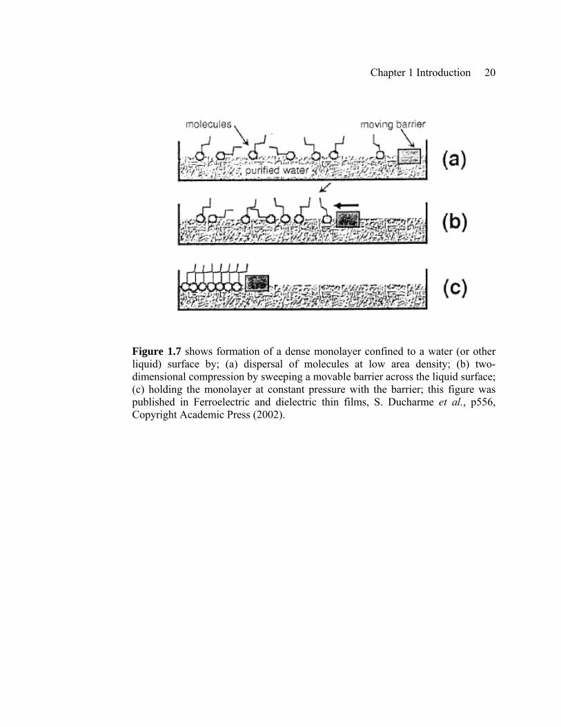
barrier. (see Figure 7) The densely formed Langmuir film on the water surface now can
be transferred to a solid substrate, and they are called “Langmuir-Blodgett”(LB) films.
Langmuir film transfer can be done by both vertical and horizontal dipping. The
horizontal dipping is also called the horizontal Langmuir-Schaefer method.
Chapter 1 Introduction 20
Figure 1.7 shows formation of a dense monolayer confined to a water (or other liquid) surface by; (a) dispersal of molecules at low area density; (b) two-dimensional compression by sweeping a movable barrier across the liquid surface; (c) holding the monolayer at constant pressure with the barrier; this figure was published in Ferroelectric and dielectric thin films, S. Ducharme et al., p556, Copyright Academic Press (2002).
Chapter 1 Introduction 21
Langmuir-Blodgett Fabrication of P(VDF-TrFE) Films
P(VDF-TrFE) copolymers are not amphiphilic, however, they consist of
macromolecules with low solubility in water, and readily form metastable monolayers on
a water subphase.10,36 P(VDF-TrFE) copolymer films used for the research presented in
this dissertation were fabricated with a NIMA model 622C automated LB trough. The
routine sample fabrication procedures were as follows. The cleaned trough was filled
with de-ionized pure water with a resistivity of 18 MΩ. Then, prepared copolymer
solutions in DMSO with 0.01 ~0.06 % weight concentrations were dispersed on the water
surface. The dispersed copolymer solutions became a thin film on the water, and then the
film was to be compressed at a rate of 20~60 cm2/min by two barriers from the outside
towards the center of the trough where the pressure sensor was placed. The film
compression was performed under the pressure control. The target pressure for the films
was 5 mN/m, which is well below the collapse pressure. Once the target pressured was
reached, the copolymer films on the water were transferred to a desired substrate. The
transferring method we used was the horizontal Schafer method.

Chapter 1 Introduction 22
References
1 H. Kawai, Japan J. Appl. Phys. 8 (1969) 975
2 J. G. Bergman, J. H. McFee and G. R. Crane, Appl. Phys. Lett. 18 (1971) 203
3 A. J. Lovinger, G. T. Davis, T. Furukawa and M. G. Broadhurst, Macromolecules 15 323 (1982).
4 T. Furukawa, M. Date, and E. Fukada J. Appl. Phys. 51(2), 1135-1141 (1980)
5 T. Furukawa, and G. E. Johnson Appl. Phys. Lett. 38(12), 1027-1029 (1981)
6 T. T. Wang, J. M. Herbert, and A. M. Glass, Eds., “The Applications of Ferroelectric Polymers.”
Chapman and Hall, New York, 1988.
7 T. Furukawa, Phase Transitions 18, 143 (1989)
8 A. V. Sorokin, V. M. Fridkin, and V. M. Fridkin J. Appl. Phys. 98, 044107 (2005)
9 M. C. Petty, Langmuir-Blodgett films: an introduction (Cambridge University Press, 1996)
10 S. Ducharme, S. P. Palto, and V.M. Fridkin, in Ferroelectric and dielectric thin films, edited by H. S.
Nalwa (Academic press, 2002)
11 Kwan Chi Kao Dielectric phenomena in Solids (Elsevier, Inc, 2004)
12 L. D. Landau , Zh. Eksp. Teor. Fiz. 7, 627 (1937)
13 L. D. Landau, Phys. Z. Sowjun. 11, 545 (1937)
14 L. D. Landau and E. M. Lifshitz, Statistical Physics: Part I. (Pergamon, Oxford, 1980)
15 V. Ginzburg, Zh. Dksp. Teor. Fiz. 15, 739 (1945)
16 V. Ginzburg, J. Phys. USSR 10, 107 (1946)
17 V. Ginzburg, Zh. Eksp. Teor. Fiz. 19, 39 (1949)
18 A. F. Devonshire, Phil. Mag. 40, 1040 (1949)
19 A. F. Devonshire, Phil. Mag. 42, 1065 (1951)
20 A. F. Devonshire, Advances in Physics 3, 85 (1954)
21 R.G. Kepler, in Ferroelectric Polymers, edited by H. S. Nalwa (Marcel Dekker, New York, 1995)
22 A. J. Lovinger, Science 220 1115(1983)
23 J. B. Lando and W. W. Doll, J. Macromolecular Science-Physics B2 205 (1986)
24 J. F. Legrand, Ferroelectrics 91, 303 (1989)

Chapter 1 Introduction 23
25 K. Tashiro, in Ferroelectric Polymers, edited by H. S. Nalwa (Marcel Dekker, New York, 1995)
26 K. Tashiro, M. Kobayashi, H. Tadokori, E. Fukada, ibid., p. 691
27 T. M. Furukawa, E. Date, E. Fukada, Y. Tajitsu and A. Chiba. Jpn. J. Appl. Phys. 19, L109-L112 (1980)
28 T. Yagi, M. Tatemoto, and J. Sako, Polymer J. 12 209 (1980)
29 K. Koga and H. Ohigashi, J. Appl. Phys. 59 2142 (1986)
30 K. Koga and N. Nakano, T. Hattori, and H. Ohigashi, J. Appl. Phys. 67, 15 (1990)
31 T. Furukawa, Ferroelectrics 57, 63 (1984)
32 J. Chio, C. N. Borca, et al. Phys. Rev. B 61, 5760 (2000)
33 C. N. Borca, J. Choi, S. Adenwalla, S. Ducharme, et al. Appl. Phys. Lett. 74, 374 (1999)
34 M. Bai, A.V. Sorokin et. al. J. Appl. Phys. 95, 3372 (2004)
35 I. Langmuir, J. Am. Chem. Soc. 39, 1848 (1917)
36 E. Ferroni, G. Gabrielli, and M. Puggelli, La Chimica e L’Industria (Milan) 49, 147 (1967)
Chapter 2 Sample Characterization 24
Chapter 2 Sample Characterization
The ferroelectric properties of LB thin films of P(VDF-TrFE 70:30)
copolymers with a range of 50~200 nm thick, corresponding to 30~100 LB layers had
been thoroughly studied and reported earlier.1,2 After this establishment, some of the
characterization experiments have become our routine diagnostic measurements, such as
x-ray diffraction (XRD), capacitance vs. temperature (CT), capacitance vs. DC voltage
(CV, butterfly curve), and etc. The results of the diagnostic measurements are used to
determine the qualities of newly made samples in the lab.
According to the purpose of the diagnostic measurements mentioned above,
proper construction of samples is needed. There are three different types of samples
based on their configuration: one is thin films, the second is self-assembly structure
(Nanomesas), and the third is capacitors of both thin films and nanomesas. In this
chapter, the three types of samples are introduced with along their routine
characterization measurements. In addition to that, thickness measurements of thin films
with x-ray reflectivity and observation of nanomesa formation during annealing with
atomic force microscopy (AFM) are discussed in this chapter, and these measurements
were done for the first time in this study.

Chapter 2 Sample Characterization 25
Figure 2.1 show a sample configuration of simple continuous films deposited on Si substrate.
2.1 Thin Films
The configuration of thin films (Fig. 2.1) is the simplest form of samples that we
study. Thin films are constructed simply by depositing LB films of P(VDF-TrFE)
copolymer on a cleaned smooth substrate, such as Si wafer and highly ordered pyrolytic
graphite (HOPG) according to the procedure of Langmuir-Scheafer technique introduced
in section 1.3. Si wafer is the most commonly used substrate for structural studies of thin
film in our lab. Highly ordered pyrolytic graphite substrates (HOPG) are used for
specialized studies such as scanning tunneling microscopy (STM), or piezoelectric force
microscopy (PFM)3 where the electrical grounding of samples during the measurements
is crucial. Thin films on Si wafer with the simple configuration (Fig. 2.1) are used to
characterize the crystal structure and the thickness of thin films with x-ray diffraction
(XRD) and x-ray reflectivity (XRR), respectively. XRD has already been one of our
routine diagnostic measurements, however, XRR was first tried during the study for this
dissertation. In this section XRD and XRR will be briefly introduced, and the new results
of XRR measurements will discussed in detail later in the section 2.4.

Chapter 2 Sample Characterization 26
Figure2.2 (a) shows schematic ferroelectric structure of PVDF copolymer crystal structure based on Legrand’s report in Ferroelectrics 91, 303 (1989). The spacing between chains indicated as d is what we measure with the vertical XRD with our P(VDF-TrFE) copolymer LB thin films: (b) shows two XRD data taken from 20 LB layers of 50:50 at room temperature and at 120 ºC as indicated on the figure. At room temperature the film is in ferroelectric, β phase where dipole moments are in order and at 125 ºC the films is in paraelectric, α phase. In α phase, dipole moments are not in order anymore (see chapter1), and it results in expanded layer spacing: (c) shows XRD measurements before and after annealing on 20 LB layers of 50:50 copolymer on Si. Annealing condition was 135 ºC for 2 hours

Chapter 2 Sample Characterization 27
X-ray Diffraction (XRD)
What we measure with XRD is the out-of-plane layer spacing4 of LB thin films of
P(VDF-TrFE) copolymers. The layer spacing, d of 70:30 copolymer is approximately
0.45 nm in ferroelectric phase and 0.48 nm in expanded paraelectric phase.5 The Figure
2.2b shows XRD peaks taken from 20 LB layers of 50:50 copolymer sample measured at
room temperature (ferroelectric β phase) and at 125 ºC (paraelectric α phase) with a
Rigaku theta-two-theta diffractometer with Kα radiation from a fixed copper anode,
λ=1.54 Å. The unit cell dimensions obtained from a bulk sample of PVDF polymer are c
= 0.256 nm along the chain axis, b = 0.491 along the polarization direction, the 2-fold
axis, and a = 0.858 nm perpendicular to the chain axis. 6 The configuration of this
structure viewed from [001] direction is illustrated in Figure 2.2a. The measured spacing
d (110) peak of 50:50 copolymer was ~0.462 nm in the ferroelectric β phase, and ~0.495
nm in the paraelectric α phase as shown in Figure 2.2b. Though the dimension of d is
very similar to the spacing b (010) peak, this peak is forbidden peak to be measured. As
Figure 2.2a and b clearly presents, XRD measurements show us the crystal structure of
thin films.
The last step of the thin film preparation is annealing. Annealing enhances the
crystallinity of films and ferroelectric properties. The annealing effect on P(VDF-TrFE
70:30) LB films has been reported.7 (The shorter name 70:30 for P(VDF-TrFE 70:30)
will be used, and similarly for all the copolymers with different contents.) The example
of annealing effect on a thin film sample of 50:50 copolymer is shown in Figure 2.2c

Chapter 2 Sample Characterization 28
with XRD data before and after annealing as labeled. The increased intensity of XRD
after annealing clearly shows the improvement of the crystallinity of the 50:50 copolymer
thin film. The improvement is approximately a factor of 4, and the annealing was done at
135 ºC for 2 hours.
The absolute percentage of crystallinity of a sample cannot be determined by this
XRD measurement. However, a relative crystallinity comparison between different
samples or before and after annealing is possible since the area under the XRD peak
represents the amount of crystallized films. As a matter of fact, the XRD peak can be a
good standard to examine the quality of newly made samples. P(VDF-TrFE) copolymer
LB thin films are manually fabricated hence it is reasonable to question the
reproducibility of films. The reproducibility of films is in fact excellent. Consistent
results of XRD peak and dielectric measurements (which will be discussed later in the
section 2.3) over a decade of study are a strong indication of it.
X-ray Reflectivity (XRR)
What we measure with XRR is the thickness of thin films, and also we can
determined the LB layer transfer ratio as nm/layer by measuring thicknesses of thin film
samples with various deposited layers. This transfer ration shows us the layering property
of LB thin films. Previously variable-angle spectroscopic ellipsometry (VASE) and
capacitance measurement were used to measure sample thicknesses. The results of VASE
and capacitance measurements showed sound layering property of copolymer LB films

Chapter 2 Sample Characterization 29
over a range from 5 to 120 LB layers. 8 The film thickness determined by these
measurements is approximately 1.8 nm per 1 LB layer (1.8 nm/layer). However, these
measurements are indirect since the calculated refractive index of films were used for
VASE data analysis, and then from the result of VASE, the dielectric constant of the
films was determined for capacitance measurement analysis.8,9 In addition to that, while
our recent research focus is on thinner films, the statistics on the films less than 10 LB
layers have not been sufficiently achieved in those studies since VASE and capacitance
measurements are more accurate with thicker samples. Therefore, we chose x-ray
reflectivity (XRR) measurement to determine more accurately the thickness of films with
less than 20 LB layers.
We performed XRR measurements with a multi-purpose x-ray diffractometer, a
Bruker-AXS D8 Discover with Kα radiation from a fixed copper anode, λ=1.54 Å. XRR
measurement will be discussed in detail later in the section 2.4. The thickness of 20 LB
layers of 70:30 copolymer sample deposited on Si wafer was measured by XRR after
annealing to be approximately 37 nm, which shows an excellent agreement to the
previous studies. Therefore, a very simple, powerful, and direct thickness measurement,
XRR can be routinely used as a diagnostic measurement.
2.2 Self-assembly Structure: Nanomesas
There has been very interesting new structure found by Bai et al. during
investigation of annealing effect on thinner films with physical thickness less than 10

Chapter 2 Sample Characterization 30
nm.10,11 The new structure is ‘nanomesas’, which are self assembled structures formed
after annealing of P(VDF-TrFE) copolymer. They are shaped as isolated islands with
dimensions of approximately 100 nm in diameter, and 9 nm in thickness. Nanomesas
shown in Figure 2.3 were obtained by annealing 1 LB layer of 70:30 copolymer sample
deposited on Si wafer at 125 ºC for 1 hour.10,11 According to their study, P(VDF-TrFE)
copolymers have plastic flow when they are in paraelectric phase, and nanomesas are
manifest of it. Observation of nanomesa formation in real time has been separately
performed and shown in the section 2.5 in detail.
Morphology of Sample: Atomic Force Microscopy
Atomic force microscopy (AFM) is a very simple, convenient, and non-invasive
tool to obtain topographical images of sample by using the attractive Van der Waals force
between the AFM tip and the sample.12,13 A Digital Instrument model Dimension 3100
AFM was used for our measurements. The AFM tip used was a Si tip consisting of a
cantilever with nominal values of length, width, thickness, spring constant, and resonant
frequency of 125 μm, 35 μm, 4 μm, 40 N/m, 300 kHz, respectively. The scanning was
conducted in tapping mode which is a non-contact mode. In this tapping mode the
flexible cantilever of the AFM tip is oscillating at its resonance frequency with fixed set-
up amplitude, which corresponds to the separation between the tip and the sample surface,
and it is kept constant through the entire scanning. The interaction force between the tip
and the sample surface depends on the distance between them, and so does the oscillation
amplitude.

Chapter 2 Sample Characterization 31
Figure 2.3 is an AFM image of nanomesas formed from 1 LB layer of 70:30 copolymer sample on Si after annealing at 125 ºC for 1 hour: this Figure 2.3 is reused with permission from Mengjun Bai, Applied Physics Letters, 85, 3528 (2004). Copyright 2004, American Institute of Physics.

Chapter 2 Sample Characterization 32
Figure 2.4 (a) is an image taken from a fresh film of 1 LB layer of 50:50 copolymer on Si wafer: (b) is an image of nanomesas formed from the film shown in (a) after annealing it at 140 ºC for 1hour. First nanomesa observation was made on a 70:30 film shown in Figure 2.2b: (c) is an image of silica particles place on top of a 70:30 copolymer sample with 22 LB layers: (d) is an image taken after the silica particles (c) were washed away. In between (c) and (d) the silica particles were pressed onto the film (see Appendix B).
Chapter 2 Sample Characterization 33
The piezoelectric transducer where the AFM tip is connected controls the height of and
the oscillation amplitude of the tip according to the topography of the sample surface.
This is how an AFM collects the height information of the sample surface. The position
of the tip is detected by laser beam which is deflected off the back to the cantilever.
Some AFM images are shown in Figure 2.4. After the first observation of
nanomesas (see Figure 2.3 and 2.4b), not only to characterize nanomesas, but also
nanofabrication of samples by using the mobility of P(VDF-TrFE) copolymers films in
paraelectric phase has been our recent interest. For the nanofabrication study, observing
the morphology change in films (see Figure 2.4d) is necessary, and AFM is an ideal tool
for probing topography of thin film samples. One example of nanofabrication technique
is pressing the films with silica particles (see Figure 2.4c) called nanoimprinting, and in
Appendix B the nanoimprint work is discussed.
2.3 Capacitors
To investigate the dielectric properties of films, capacitor samples were made by
depositing LB layers of P(VDF-TrFE) copolymers on a glass substrate with the bottom
and the top Al electrodes as shown in Figure 2.5a. For glass substrates, 1 mm thick,
microscope slides, and 0.1 mm thick cover glasses are typically used. Firstly, on a clean
glass substrate, the bottom electrodes, 1 mm width stripes, were evaporated. After that
LB films of P(VDF-TrFE) copolymers films were deposited, and then, lastly top
electrodes were evaporated.

Chapter 2 Sample Characterization 34
Figure 2.5 (a) show a sample configuration of capacitor films: (b) shows capacitance vs. Temperature taken from a same 20 LB layers of 50:50 copolymer capacitor sample, and it clearly presents the thermal hysteresis and dielectric anomaly peaks at phase transition temperatures upon heating and cooling: (c) is a butterfly curve which is capacitance measured with respect to DC voltage bias from a 15 LB layers of 70:30 copolymer capacitor sample. It clearly shows switching properties of the sample: (d) is pyroelectric current switching hysteresis loop taken also from a 15 LB layers of 70:30 copolymer capacitor sample. It shows both pyroelectricity and ferroelectric switching property of the sample. (Samples of data (b) and (c) are prepared under same conditions)

Chapter 2 Sample Characterization 35
The annealing of capacitor samples has not shown clear effect, and it can be interpreted
as the performance of capacitor films is not highly dependent on the crystallinity of films.
Phase Transition: Capacitance vs. Temperature (CT)
The presence of the ferroelectric-to-paraelectric phase transition of LB thin films
of 70:30 copolymer has been confirmed by capacitance vs. temperature (CT)
measurement. 14,15 ,16,17 The CT measurements showed the dielectric anomalies at the
phase transition temperature according to the Curie-Weis law, )/()( cTTCT −=ε
where ε is a dielectric constant, C is Curie-Weis constant, T is a measurement
temperature, and CT is the transition temperature. Also the CT showed thermal hysteresis
upon heating and cooling. This thermal hysteresis is an indication of the first-order phase
transition. Figure 2.5b is a CT measurement from a 50:50 copolymer capacitor film with
20 LB layers deposited on Si wafer. It clearly shows that thermal hysteresis, and the
phase transition temperatures are approximately 70 ºC upon heating and 60 ºC upon
cooling. The measurement was performed with an impedance analyzer, the model
Hewlett-Packard 4192A. The AC signal used for the capacitance measurement was 0.1 V
at 1 kHz. The sample was ramped with a rate of 1 ºC/min up to 125 ºC, and then cooled
down to room temperature with the same ramping rate. This simple CT measurement is a
very solid and reliable tool to determine the quality of samples by comparing the
consistency of the measured phase transition temperatures and the peak heights of a
newly made sample to the prototype sample.

Chapter 2 Sample Characterization 36
Switching: Capacitance vs. Voltage Bias (CV) and Pyroelctric current hysteresis loop (Ip)
The CT measurement alone is not sufficient to prove the films are ferroelectric
because, in principle, dielectric anomaly can be seen at most phase transitions, not
necessarily ferroelectric phase transition, even though the thermal hysteresis phenomena
can be a supporting proof of ferroelectricity. Therefore, any measurements show
switching property of the films can be good complementary measurements to prove
ferroelectricity of the films. The CV curves and pyroelectric current hysteresis loop (IP)
measurements are the routine switching measurements for ferroelectric polymers and the
results of those measurements on 70:30 copolymer films are have been reported.15,18
Figure 2.5c and d show respectively CV and IP measurements recorded from two
70:30 copolymer capacitor samples prepared under the same conditions. The capacitors
consisted of an area of 1 mm2 with 15 LB layers of 70:30 copolymer films sandwiched
between Al electrodes each about 100 nm thick on a cover glass substrate. CV was
recorded with the impedance analyzer, 4192A with an AC signal of 0.1 V at 1 kHz. CV
curves basically show the change of capacitance with respect to DC voltage. The DC
voltage sweep was done at 1.5 V/min between +/-10V for two cycles. Polarization
switching from one direction to the opposite direction occurs at voltages where the two
peaks of capacitance are placed. The two peaks indicate the increased energy in the
capacitor due to the switching, and the voltages where the switching occurs are called
coercive voltages, and they are approximately 2.6 ± 0.2 V. The direction of the

Chapter 2 Sample Characterization 37
macroscopic polarization is relative to the direction of the applied DC voltage to the
sample.
The pyroelectric current measurements reveal pyroelectric property of copolymer
samples as well as switching property. As it was shortly mentioned in chapter 1, the
ferroelectric materials also have pyroelectric and piezoelectric properties, which all
originate from the noncentrosymmetric crystal structure.19 The temperature increase or
decrease causes a change in the spontaneous electric polarization in ferroelectric (or
pyroelectric) materials. If the ferroelectric materials are in contact with metal electrodes,
then the change in electric polarization will give rise to a change in compensating charges
on the electrodes. Therefore, this change will produce a current in an external circuit. The
switching of the polarization direction will be manifested as switching of the direction of
the current in the circuit. For the pyroelectric current measurement shown in Figure 2.5d,
He-Ne laser with 8 mW of the maximum power was used to change the sample
temperature by illuminating the sample with the laser beam, chopped at a frequency of 2
kHz.20 This modulated laser beam provides an oscillating temperature in the sample.
Therefore, the pyroelectric current, )/(/ dtdTpdtPdI p == was produced, where
dTPdp /= , called the pyroelectric coefficient . The current was collected with a lock-in
amplifier referenced to the chopping frequency. The lock-in amplifier is a model SR850
DSP from Stanford Research Systems. Before the current measurement the sample was
poled with DC voltage shown in x axis of the plot. While the current was collecting, the
DC voltage was removed namely field-off process, so the switching is from the steady

Chapter 2 Sample Characterization 38
state polarization. The pyroelectric current hysteresis loop in Figure 2.5d clearly shows
switching property of the copolymer films and the coercive voltage is 5.0 ± 0.5 V,
corresponding to the coercive field of 185 ± 15 MV/m (taking into account the thickness
of 1 LB layer is approximately 1.8 nm)21 . It shows good agreement with previous
reports.1,18,22 The coercive voltage, VC determined by CV curve is 50 % smaller than the
value determined by IP hysteresis loop. This could be due to slow switching nature of the
P(VDF-TrFE) copolymer films. The complete switching of a whole sample may require
100s or more11, therefore CV measurement of 1.5 V/min rate likely show partial
switching of the sample while IP loop was taken for 15 minutes per 1 V step. This is also
a general trend that the peak of CV occurs at lower voltages than VC of IP loop.
2.4 Thickness of P(VDF-TrFE) Thin Films
In this section thicknesses of P(VDF-TrFE) thin films consisting less than 20 LB
layers measured with XRR will be discussed in detail as mentioned in the section 2.1.
2.4.1 Introduction
Motivation
A distinguishing property of Langmuir-Blodgett (LB) thin films of P(VDF-TrFE)
copolymers is the easy thickness control in nanometer scale. As it has been introduced in
Chapter1, LB films of P(VDF-TrFE) are deposited layer by layer by transferring the
Langmuir copolymer film dispersed on the top of the water subphase. The multi-sample
analysis of 70:30 copolymer films from 5 to 125 LB layers were investigated with

Chapter 2 Sample Characterization 39
variable-angle spectroscopic ellipsometry (VASE) and capacitance measurements by Bai
et al.21 His work has shown a very nice linear relation between the measured thicknesses
of the films vs. the number of layers deposited. This linear relation indicates the excellent
layering property of copolymer thin films made by LB technique.
The layering transfer ratio of 70:30 copolymer films determined from
ellipsometry was 1.8 nm/layer. The study, however, was heavily weighed with thicker
films, more than 20 LB layers21, because spectroscopic measurements are less accurate
with thinner samples. The study of thinner ferroelectric films requires more accurate
measurements of their thicknesses. Therefore, we looked for new tool to measure the
thickness of thinner films, and X-ray reflectivity (XRR) was chosen. XRR is an optimal
tool to measure the thinner films because XRR is known for its atomic scale sensitivity,
and the range of the measurable film thickness is from 0.1 to 500 nm.23 XRR studies on
other polymer thin films, and other LB films can be found in books written by M. Tolan24,
and J. Daillant.25
Study Plan and Sample Preparation
We designed the thickness study with two types of samples. The first type of
samples had thicknesses typical of most commonly used copolymer samples in our lab,
which are 15 to 30 LB layers, and to compare the results to the value, 1.8 nm per layer
obtained by ellipsometry study. We expected that the results of the first type could give
us a good comparison with ellipsometry results demonstrating on the usefulness of XRR

Chapter 2 Sample Characterization 40
measurements on our LB copolymer thin film system. The second type consisted of
thinner samples, from 1 to 11 LB layers, and then obtain the transfer ratio (or average
thickness of films per layer) of the thinner films. XRR is not suitable for thin films with
more than 5 nm of the roughness and XRR measurements on those rough films will result
in null data. Therefore, obtaining useful XRR data themselves will manifest the quality of
thinner LB copolymer films, such as the smoothness and the uniformity.
Three copolymers, 70:30, 50:50, and 80:20 were used to make films. Thin films
of 20 LB layers as a prototype samples used in our lab, and a series of films with 1 to 11
LB layers of each copolymer were prepared. All samples were deposited on Si wafers,
approximately 500 micron thick under the same deposition conditions on the LB trough,
and those conditions are described in Chapter1. The size of the samples were
approximately 1 ~ 4 cm2.
2.4.2. Measurements
XRR measurements were performed on a multi-purpose x-ray diffractometer, a
Bruker-AXS D8 Discover with Kα radiation from a fixed copper anode, λ=1.54 Å. The
width of the slit used for all measurements was 0.2 mm. Scan conditions were set at the
scan interval as 0.005 º in 2θ , and the scanning rate as 1~5 sec/step. This scan condition
is relatively slow scan compared to the typical scan condition 0.01º of scan interval and 1
sec/step of scanning time. For a series of thinner samples, XRR measurements were
performed only on the fresh samples as deposited without annealing.

Chapter 2 Sample Characterization 41
Figure 2.6 illustrates the x-ray beam path in x-ray reflectivity measurement.

Chapter 2 Sample Characterization 42
Since the thinner films undergo drastic morphology change after annealing,10,11
comparing the thickness of the films before and after annealing are not meaningful. The
films with 20 LB layers were measured both before and after annealing. The annealing
was done at 135 ºC for 2 hours in a closed thermal stage with heating and cooling rate of
1 ºC/min.
Relation of X-ray interference pattern and the Film thickness
Similar to visible light, x-ray radiation is also refracted and reflected at the
interface between two media and follows Snell’s law as shown in Figure 2.6. The thin
film shown in Figure 2.6 is a single material layer.a In this work all copolymer thin film
samples were a single material layer system so they have only two interfaces; air-film,
and film-substrate as schematically shown in Figure 2.6. Also, here we only treated the
specular reflection, and did not account for diffuse reflection.
During the x-ray reflection measurement, the x-ray reflected from the air-film
interface will interfere with the x-ray reflected from the film-substrate interface, and
collected XRR data will show the interference pattern. Then, we can determine the
thickness of the film by analyzing the interference pattern with the thin film interference
equation for either the constructive interference or the destructive interference. However,
a This material layer is a different concept from the LB layer. A stack of a number of LB copolymer layers is one material layer which we consider homogeneous for the present study. This material layer we talk about in XRR study depends on the refractive index of the material similarly the mass density of the material.

Chapter 2 Sample Characterization 43
the distinguishing property of x-rays from the visible optical light is the refractive index
of films, n for x-ray radiation is very close to unity, and it is
βδ in −−= 1 (2.1)
where δ is the dispersion factor, and β is the absorption factor. The dispersion factor, δ
for soft materials is an order of 10-5 and the absorption factor is approximately 3 orders
less than the dispersion factor26, therefore we assume negligible x-ray absorption for this
study. The effect of the refractive index being close to unity results in a rapid decrease in
Fresnel reflectivity27 (the reflectivity with respect to the angle of incidence) with angle θ
right after the critical angle θc , below which the total reflection occurs. Therefore, the
region of interest for XRR measurements is the small incident angle region where
reflectivity is high in intensity. Note that the critical angle can be expressed in terms of
the dispersion factor, δθ 2=c24,25 and the Fresnel reflectivity of x-ray decays
proportion to 1/ 4θ , for cθθ 3⟩ , where θ is incident angle. Based on our measurements,
XRR data became noisy above 8º in 2θ for films thinner than 10 nm, and above 2º in 2θ
for films thicker than 10 nm. Since we are only working in the small angle region, the
small angle approximation was applied for the analysis of XRR data.
The thickness, t of the thin films can be determined by using the thin film
interference equation in general. Following equation is for the destructive interference
....3,2,1,)21(sin2 =−= mmt t λθ (2.2)

Chapter 2 Sample Characterization 44
where λ is the wavelength of x-ray, 1.54Å for our measurement, and tθ is the refracted
angle of x-ray in the film (Fig. 2.6). Eq. 2.2 can be modified for XRR by applying the
small angle approximation and Snell’s law ( tn θθ coscos = ) into the equation. The
modified thin film equation for destructive interference is as following
222
22 )
21(
4 cm mt
θλθ +−= (2.3)
where mθ is the incident angle θ indexed with the destructive interference fringe number
m. Kiessig developed this method of analysis so it bears his name, the interference fringes
in XRR are called Kiessig fringes, and the thickness determination method using the
modified thin film interference equation (Eq. 2.3) is called the Kiessig fringe method.
In the rest of this section the Kiessig fringe method will be reviewed (see Fig. 2.7), and
this method was our main tool for the study of film thickness by x-ray reflectivity.
Kiessig Fringe Method
Firstly, XRR measurements were recorded, and then the minimum positions of
the interference fringes, mθ in the θ axis were read from XRR data. After finishing
assigning mθ , the graph of 2mθ vs. 2)2/1( −m was plotted and fit to the linear regression
model, and then the parameters t and cθ were extracted from the slope and the y
intercept of the fit, respectively. The film thickness t was calculated using Eq. 2.3, where
slope= 22 4/ tλ .

Chapter 2 Sample Characterization 45
Figure 2.7 illustrates the Kiessig fringe method, the thickness method that we used for this study. XRR data from a 20 LB layer film of 70:30 copolymer is shown in the main plot. Positions of the minima of Kiessig fringes are indicated as θm, and then they were plotted according to the modified Bragg equation and shown in the sub-plot.

Chapter 2 Sample Characterization 46
As described above, the Kiessig fringe method is really simple. However,
assigning the correct order m to the first apparent fringe in the data is very important,
therefore it needs to be done carefully. That is because not always the first apparent
fringe namely 0θ in the data is the real first fringe m=1. The first few fringes can be
placed below cθ , therefore hidden in the data. This depends on the thickness and the
density of the sample. For example, for the XRR data shown in Figure 2.7, 0θ is 2θ , in
other words the first apparent minimum is in reality the second destructive interference,
or m=2. When 0θ is correctly assigned, data points in 2mθ vs. 2)2/1( −m plot should
make a straight line, especially at small angles, and when it is incorrectly assigned, it will
result in a distortion of the straight line, and an incorrect thickness of the film. To choose
correct order for 0θ we plotted 2mθ vs. 2)2/1( −m with different 0θ , and tested the
straightness of 2mθ vs. 2)2/1( −m plot with the goodness of the line fit.
2.4.3 Results
All XRR data recorded for this study is shown in Figures 2.8 and 2.10. The
thicknesses of all samples were determined by Kiessig fringe method introduced in the
previous section, and the results are tabulated in Table 2.1. In case of the thinner samples,
the transfer ratio (nm/layer) of each copolymer is shown rather than presenting thickness
of all individual samples. The transfer ratio was determined by fitting a plot of ‘the
thickness of film vs. the number of layers of the film’ for each copolymer films, as shown
in Figure 2.11.
Chapter 2 Sample Characterization 47
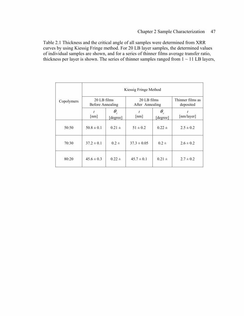
Table 2.1 Thickness and the critical angle of all samples were determined from XRR curves by using Kiessig Fringe method. For 20 LB layer samples, the determined values of individual samples are shown, and for a series of thinner films average transfer ratio, thickness per layer is shown. The series of thinner samples ranged from 1 ~ 11 LB layers,
Kiessig Fringe Method
20 LB films Before Annealing
20 LB films After Annealing
Thinner films as deposited
Copolymers
t [nm]
cθ [degree]
t [nm]
cθ [degree]
t [nm/layer]
50:50 50.8 ± 0.1 0.21 ± 51 ± 0.2 0.22 ± 2.5 ± 0.2
70:30 37.2 ± 0.1 0.2 ± 37.3 ± 0.05 0.2 ± 2.6 ± 0.2
80:20 45.6 ± 0.3 0.22 ± 45.7 ± 0.1 0.21 ± 2.7 ± 0.2

Chapter 2 Sample Characterization 48
Figure 2.8 shows XRR data from 20 LB layers of each copolymer are shown here (a) before and (b) after annealing. The annealing was done at 135 ºC for 2 hours.

Chapter 2 Sample Characterization 49
Figure 2.9 shows three simulated XRR curves of a single layer thin film model. The thin film model has the thickness 37 nm, and the density 1.97 g/cm3 corresponding to the critical angle approximately 0.2º when considering the film is 70:30 copolymer. As it is indicated on the plot, XRR in black is when there is no roughness in the sample, XRR in red is when there is about 2 nm of the roughness on the film-Si interface, and XRR in Blue is when there is about 2 nm of the roughness on the Air-film interface. This simulation convinced us that the smeared fringes in our data should be dominantly from the film-Si interface roughness.
Chapter 2 Sample Characterization 50
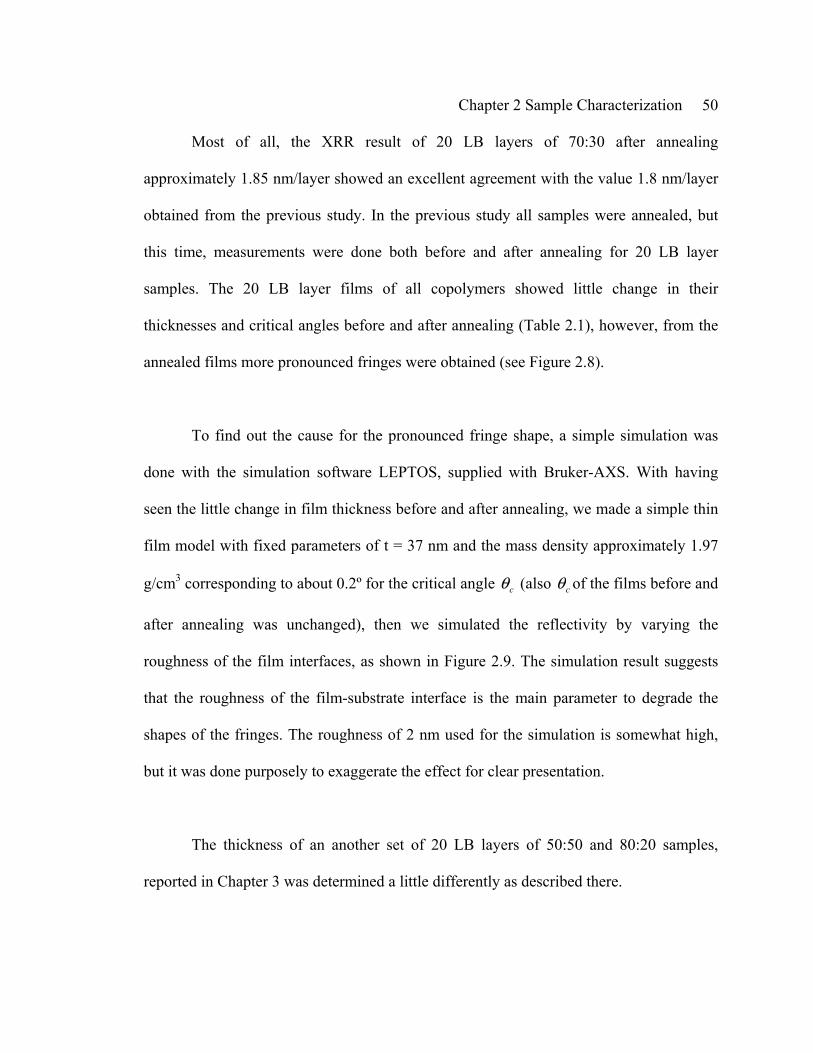
Most of all, the XRR result of 20 LB layers of 70:30 after annealing
approximately 1.85 nm/layer showed an excellent agreement with the value 1.8 nm/layer
obtained from the previous study. In the previous study all samples were annealed, but
this time, measurements were done both before and after annealing for 20 LB layer
samples. The 20 LB layer films of all copolymers showed little change in their
thicknesses and critical angles before and after annealing (Table 2.1), however, from the
annealed films more pronounced fringes were obtained (see Figure 2.8).
To find out the cause for the pronounced fringe shape, a simple simulation was
done with the simulation software LEPTOS, supplied with Bruker-AXS. With having
seen the little change in film thickness before and after annealing, we made a simple thin
film model with fixed parameters of t = 37 nm and the mass density approximately 1.97
g/cm3 corresponding to about 0.2º for the critical angle cθ (also cθ of the films before and
after annealing was unchanged), then we simulated the reflectivity by varying the
roughness of the film interfaces, as shown in Figure 2.9. The simulation result suggests
that the roughness of the film-substrate interface is the main parameter to degrade the
shapes of the fringes. The roughness of 2 nm used for the simulation is somewhat high,
but it was done purposely to exaggerate the effect for clear presentation.
The thickness of an another set of 20 LB layers of 50:50 and 80:20 samples,
reported in Chapter 3 was determined a little differently as described there.

Chapter 2 Sample Characterization 51
Figure 2.10 shows XRR data of all thinner films of each copolymer samples as indicated in the plots are shown here. The blue numbers on the data lines is the number of LB layers of the sample the data were taken from. The XRR data from 1~2 LB layer samples of all copolymers show clear oscillations implying the films are uniform. All data were taken from un-annealed samples.

Chapter 2 Sample Characterization 52
Figure 2.11 shows the plots of the transfer ratio determination for each copolymer as indicated. Each data point in these plots is the thickness of corresponding XRR shown in Figure 2.9. (Some data points without error bars are from XRR curves that have only 2 measurable minima. The uncertainty shown in the ratio values is obtained from the uncertainty in the slope of the fit lines.)
The previous analysis was done with an assumed dispersion factor δ=6.31×10⁻⁶
without distinction between copolymers and PVDF polymer. This value was obtained,
based on the relation δ=(λ2/2π)reρe, introduced in Tolan and Daillant books,24,25 where re
is the classical electron radius, and ρe the electron density. For the estimation ρe of PVDF
polymer was used.
In the case of thinner samples, they showed thicker layering for all three
copolymers, on average compared to the 20 LB layer films: 2.7 nm/layer, 2.6 nm/layer,
and 2.5 nm/layer for 50:50, 70:30, and 80:20 copolymers, respectively (see Fig. 2.11).
The thicker layering below 20 LB layer samples was also apparent in the previous study
of Bai et al. (see Fig. 6a of ref. 21). A possible stronger interaction between the film and
the substrate for thinner samples could result in the thinker transfer ratio. Unlike the 20

Chapter 2 Sample Characterization 53
LB layer sample results, thinner films of 50:50 copolymers did not particularly show a
thicker layering than 70:30 and 80:20.
Discussion
In this study, the thickness of the silicon oxide layer was not carefully
considered; therefore to improve the accuracy of the thickness determination the
thickness of oxide layer should be looked into in the future study. Also some of the
samples among thinner samples did not show good quality of XRR. These samples with
poor quality XRR showed rocking curves with split peaks during XRR measurement set-
up. Similar split rocking curves were observed from bare Si substrates. We suspected,
thus, this problem was originated from the quality of the Si wafer, however, we did not
look into the problem in depth.
The roughness of the interfaces cannot be determined with the Kiessig fringe
method. We tried to look at the roughness of our sample by fitting XRR with
LEPTOS.24,25,28 We fit the thickness and the mass density of the film, and the roughness
of both the air-film and film-substrate interfaces by giving a reasonable initial values for
thickness and density by using the results from Kiessig method. However, we have not
obtained any good results. Fitting XRR data is another area to look into in the future.
Conclusion
We have acquired XRR data from even 1 LB layer samples (Fig. 2.10). This
strongly supports that one layer of LB copolymer film is sufficiently uniform enough to

Chapter 2 Sample Characterization 54
obtain valuable XRR data over a large area on order of mm2. Also, the thickness of the
80:20 and 50:50 copolymer LB films were measured for the first time in this study. The
thickness measured from 20 LB layer films of 70:30 copolymer sample using XRR
showed an excellent agreement with the results obtained from the ellipsometry
measurement. The quality of Si substrate such as miscut and the thickness of the silicon
oxide layer need to be carefully considered to obtain improved XRR data in the future
especially for thinner films where strong influence from the substrate is suspected.
2.5 Real-Time Observation of Nanomesa Formation
In this section observation of nanomesa formation in real-time is presented.
Previously nanomesas were observed only after annealing10; however, here we directly
observed how the film as deposited formed into nanomesas during annealing with atomic
force microscopy (AFM).
2.5.1 Measurement
We have observed nanomesa formation during annealing on the stage of an
atomic force microscopy (AFM) by taking images at about every 10 ºC steps. The AFM
system used for the observation is Vecco MultiMode NS-IIIA. This system provides
three different temperature ranges of heating/cooling elements namely temperature
controllable scanners. The three temperature ranges are for air and inert gasses; -35 ºC to
100 ºC, ambient to 250 ºC, and -35 º to 250 ºC.29 The heating element, used for this
observation was the second range from ambient to 250 ºC. The sample was mounted on

Chapter 2 Sample Characterization 55
the top of the scanner with thermal conducting tape, and the temperature of the system
was controlled by the current controller provided with the heating scanner. The
temperature from one temperature to the next temperature (5~10 ºC steps) was increased
approximately at a rate of 1 ºC/min, and then the increase of the temperature was
interrupted by a 5 min of soaking time. After the soaking, the temperature was stabilized
and ready for scanning, and then 2~6 images were recorded at each temperature. The
reason why we recorded a few number of images at one temperature is to the time
dependence of the film separation at a fixed temperature. One image took approximately
9 min. Over all the experiment, the temperature was increased from room temperature
(25 ºC) to 135 º at an average rate of approximately 10 ºC/hr. All images were recorded
in non-contact tapping mode. The spring constant of the AFM tip used for this study was
mNk /42= , and the resonant frequency of the cantilever of the tip was approximately
320 kHz.
2.5.2 Results
We were able to reach a sample temperature 135 ºC with no difficulties. However,
at 135 ºC the tip-surface contact was lost a couple of times. We attributes the lost contact
to the fact that the films were in the high energy state of paraelectric phase with plastic
flow.10,11 It is also assumed that the flow of the material became very active at 135 ºC
getting close to its melting temperature, 150 ºC.30 The results of this real-time observation
on nanomesa formation showed an excellent agreement to the previous studies done by
Bai et al..10,11 He showed the morphology change of 1 LB layer of 75:25 copolymer with

Chapter 2 Sample Characterization 56
respect to the annealing temperature (Fig. 2.12). The images shown in Figure 2.12 were
taken at room temperature after annealing by Bia. The indicated temperatures on the
images are annealing temperatures. The set of images shown in Figure 2.13 are from this
work, the real-time observation of nanomesa formation. In Figure 2.13 the temperatures
indicated on the images are scanning temperatures at which the images were recorded.
What these images reveal is that the film separation is not reversible process
because the amount of separation occurred during annealing seems to be preserved after
the annealing. It is clear if we compare images between Figure 2.12 and Figure 2.13
indicated with the same temperatures of annealing (for 2.12) and scanning (for 2.13). The
morphology of the film did not show much difference from the fresh sample as deposited
(Fig. 2.13). The separation of film started from 60 ºC and started to form isolated films
from 90 ºC (Fig. 2.13). This isolated films formed at 90 º are the early form of nanomesas.
The development of the height, h with respect to the temperatures is shown in
Figure 2.14 with some examples. The example images (Fig. 2.14a, b, and c) were
selectively chosen among the images shown in Figure 2.13. The line profiles presented in
Figure 2.14e, f, and g are from the parts, highlighted with blue lines in Figure 2.14a, b,
and c, respectively. This clearly shows that the increase of h was followed by film
separation. This increase of the h is plotted in Figure 2.15a.
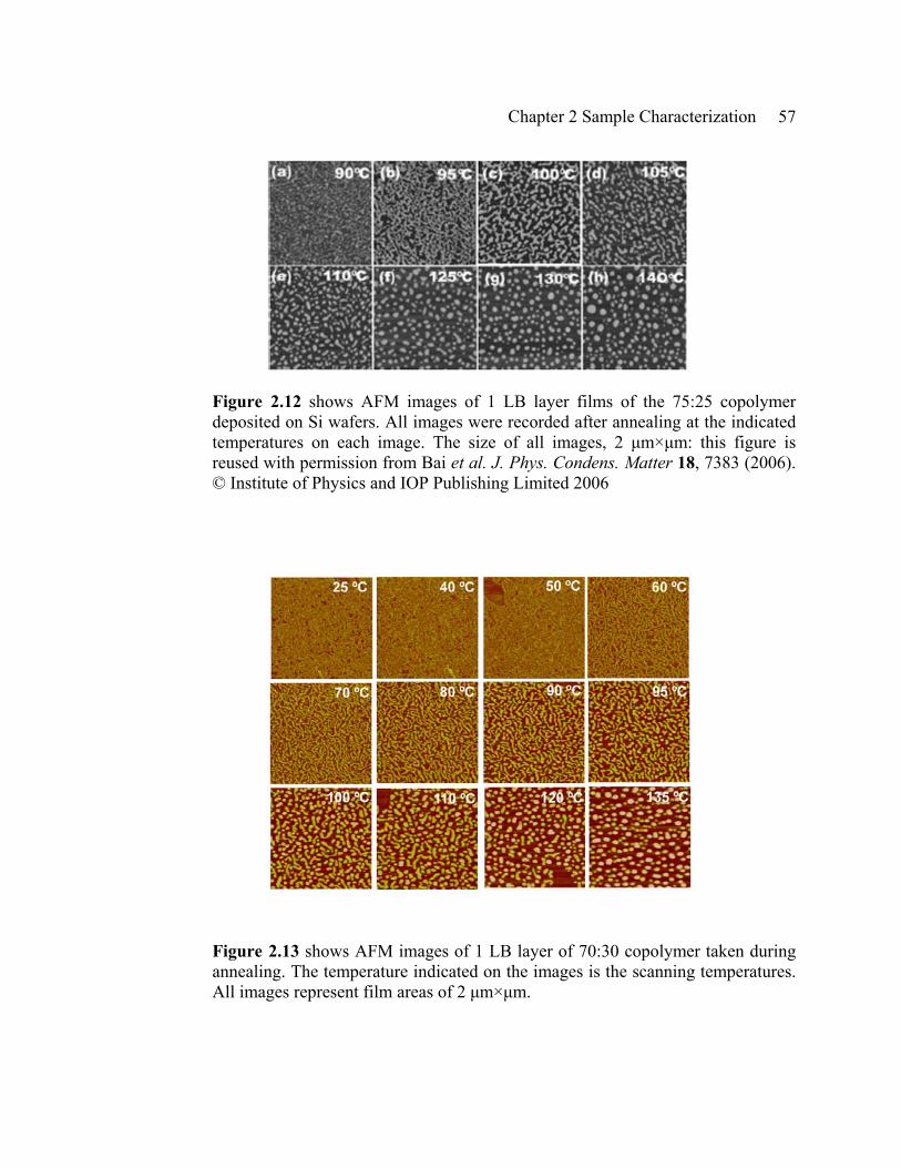
Chapter 2 Sample Characterization 57
Figure 2.12 shows AFM images of 1 LB layer films of the 75:25 copolymer deposited on Si wafers. All images were recorded after annealing at the indicated temperatures on each image. The size of all images, 2 μm×μm: this figure is reused with permission from Bai et al. J. Phys. Condens. Matter 18, 7383 (2006). © Institute of Physics and IOP Publishing Limited 2006
Figure 2.13 shows AFM images of 1 LB layer of 70:30 copolymer taken during annealing. The temperature indicated on the images is the scanning temperatures. All images represent film areas of 2 μm×μm.

Chapter 2 Sample Characterization 58
Figure 2.14 shows the height development of the film with respect to the scanning temperatures. As the film starts the separation, it developed its height due to conservation of the material.
The h of films was measured by using the roughness analysis option in NanoScope
software (a scanning microscope image analysis tool), equipped with the Vecco AFM
system. The height analysis shown in Figure 2.15a makes excellent agreements with our
two different previous studies. One is the onset temperature of paraelectric phase upon
heating. This plot clearly shows the drastic change that occurred at 60 ºC as marked with
an arrow and one of our previous x-ray diffraction studies on 70:30 copolymer films
showed a drastic increase of paraelectric phase material at 60 ºC.7 The other is the linear
trend of the height increase. Both the real time observation and Bai’s annealing study11
shown in Figure 2.15b show the height increase approximately at a rate of 1nm per 10ºC.

Chapter 2 Sample Characterization 59
Figure 2.15 (a) shows the increase of the average height of 1 LB layer of 70:30 copolymer film deposited on Si wafer as it was heated and (b) is the average heights of 1 LB layers of 75:25 copolymer deposited on Si wafer after they were annealed at different temperatures as it is indicated.3: Figure 2,15b is reused with permission from Bai et al. J. Phys. Condens. Matter 18, 7383 (2006). © Institute of Physics and IOP Publishing Limited 2006
Figure 2.16 (a) shows the decrease of the mean diameter of 1 LB layer of 70:30 copolymer film deposited on Si wafer as it was heated.

Chapter 2 Sample Characterization 60
Also the mean lateral size of the nanomesa was analyzed and plotted in Figure
2.16. The determination of the lateral size (diameter) of nanomesas was done with the
same image analysis software, NanoScope software. This analysis is only applicable to
the images of particle-like films, in other words, only films with completely isolated
areas. This complete isolation in the film (an early form of nanomesas) happened above
90 ºC. The diameter, D shows linear decrease up to 110 ºC, and the decrease became
unclear beyond that point. This phenomenon seems less obvious in h change.
All data points in Figure 2.15 and 16 were obtained from different images taken at
the assigned temperatures in the plot. The size of the images is ranged from 1 to 4 μm2. In
general 1 μm2 images have better resolution than 4 μm2. This could result in obtaining a
smaller h and d of nanomesa dimensions from the images recorded over a larger area due
to the lower resolution as it is schematically illustrated in Figure 2.17. Therefore, this
artifact could have contributed the large uncertainty of h and D values among the images
recorded at the same temperature. If all the images were taken at one size, then the
following two equations (2.4) and (2.5) can be used to test if the distribution of h and D is
originated from the kinetic change of the film. The equations are obtained from the
volume conservation, which assumes, reasonably, that the nanomesas do not exchange
mass once separated, or split or recombine.
rh
hhh
etemperaturfixedattempfixedatinitial
final 1
max
min ≡⎟⎟⎠
⎞⎜⎜⎝
⎛=⎟⎟
⎠
⎞⎜⎜⎝
⎛ (2.4)
rDD
DD
etemperaturfixedattempfixedatinitial
final ≡⎟⎟⎠
⎞⎜⎜⎝
⎛=⎟⎟
⎠
⎞⎜⎜⎝
⎛
min
max (2.5)

Chapter 2 Sample Characterization 61
If the data provides the same r from both h data and D data, then it can be concluded that
the distributions in the data is originated from a kinetic morphology change. However, in
this study this analysis was not applicable.

Chapter 2 Sample Characterization 62
Figure 2.17 is a schematic cartoon to show expected artifact in AFM images analysis due to image resolution related to the size of images. With low resolution image we could be obtained smaller values of the heights and the diameters of isolated films.

Chapter 2 Sample Characterization 63
References 1 S. Ducharme, S. P. Palto, and V.M. Fridkin, in Ferroelectric and dielectric thin films, edited by H. S.
Nalwa (Academic press, 2002)
2 L M Blinov, V M Fridkin et al. Physics Uspekhi 43, 243-257 (2000)
3 B. J. Rodriguez, S. Jesse, and S. V. Kalinin et al. Appl. Phys. Lett. 90, 122904 (2007)
4 J. Choi et al, Phys. Rev. B 61, 5760 (2000)
5 S. Ducharme et al, Phys. Rev. Lett. 84, 175 (2000)
6 J. F. Legrand, Ferroelectrics 91, 303 (1989)
7 M. Poulsen, Use of an External Electric Field to Convert the Paraelectric phase to the Ferroelectric Phase
in Ultra-Thin Copolymer Films of P(VDF-TrFE), B.S. Thesis, University of Nebraska, Lincoln, 2000.
8 A. V. Bune et al J. Appl. Phys. 85 7869 (1999
9 M. Bai et al. J Appl. Phys 84, 195 (2003)
10 M. Bai and S. Ducharme, Appl. Phys. Lett. 85 3628 (2004)
11 M. Bai, M. Poulsen, and S. Ducharme, J. Phys. Condes. Matter 18 7383 (2006)
12 V. J. Morris, A. R. Kirby, and A. P. Gunnin, Atomic Force Microscopy for Biologists (Imperial College
Press, London, 1999)
13 S. H. Cohen and M. L. Light Body, Atomic Force Microscopy/ Scanning Tunneling Microscopy 2 (New
York:Plenum Press, 1997)
14 S. Palto et al. Ferroelectrics Lett. 19, 65 (1995)
15 A. V. Bune et al. Appl. Phys. Lett. 67, 3975 (1995)
16 L. M. Blinov et al. Thin Solid Films 284, 474 (1996)
17 A. V. Sorokin et al. Mo. Mater. 6, 61 (1996)
18 A. V. Sorokin et al. J. Appl. Phys. 98, 044107 (2005)
19 Kwan Chi Kao, Dielectric Phenomena in Solids (Elsevier, Inc, 2004)
20 A. V. Bune et al J. Appl. Phys. 85 7869 (1999)
21 M. Bai et al. J. Appl. Phys. 95, 3372 (2004)
22 S. Ducharme et al, Phys. Rev. Lett. 84, 175 (2000)

Chapter 2 Sample Characterization 64
23 http://www.bruker-axs.de (the website of Bruker AXS)
24 M. Tolan ‘X-ray Scattering from Soft-Matter Thin Films’ (Spinger-Verlag Berlin Heidelberg, 1999)
25 J. Daillant, and A. Gibaud ‘X-ray and Neutron Reflectivity: Principles and Applications’ (Springer-
Verlag Berlin Heidelberg New York, 1999)
26 F. Huang, ‘X-ray Reflectivity Studies of Thin Film’ Internal Report (Center For Materials For
Information Technology, An NSF Science and Engineering Center)
27 E. Hecht Optics ( Addison-Wesley Canada, 1987)
28 Bruker AXS, LEPTOS Analytical Software for XRD and XRR, User’s manual
29 The website of the manufacturer of the system, http://www.veeco.com
30 K. Koga and N. Nakano, T. Hattori, and H. Ohigashi, J. Appl. Phys. 67, 15 (1990)

Chapter 3 Polarization Interaction
65
65
Chapter 3 Polarization Interaction
in Multilayered Thin Films of P(VDF-TrFE)
In this chapter the investigation on the effect of polarization interaction occurred
in multilayered films of 80:20 and 50:50 copolymers are presented.a
3.1 Introduction
The role of finite-size effects in ferroelectric materials is less clear, though of
critical importance in the rapidly growing ferroelectric memory industry, where the
bistability of polarization of thin ferroelectric films is paramount. Analyses using mean
field theory generally conclude that the depolarization field energies and surface energies
will suppress ferroelectricity. 1 , 2 There were several early observations of finite-size
effects in ferroelectric oxide thin films3,4,5 as thin as 100 nm, and of nanoparticles as
small as 25 nm,6 , 7 although these results were probably dominated by variations in
sample composition or microstructure. 8 Improvements in the fabrication of thin
perovskite films pushed the limit below 15 nm, 9 , 10 , 11 , 12 , 13 in accordance with the
predictions of first-principles calculations.14,15 Ferroelectricity has been reported in films
as thin as 1 nm in both polymers16 and oxides.17 The most remarkable results of the thin
film studies were that reduced thickness does not necessarily decrease the Curie
temperature or spontaneous polarization. Though polarization measurements of the
a This chapter has been published in Journal of Condensed Matter, 19 086206 (2007). Minor changes from the original Journal has been made for this dissertation.

Chapter 3 Polarization Interaction
66
66
thinnest ferroelectric polymers are inconclusive,16 a recent study of BaTiO3 thin films
with SrRuO3 electrodes showed significant polarization decline only below 15 nm,18 and
studies of unit cell tetragonality in PbTiO3 films,19 also indicates a significant decrease in
polarization below 10 nm in thickness.
Studies of ferroelectric multilayers and superlattices, composed of ferroelectric
oxides with different bulk transition temperatures (TCs) or of ferroelectric and
paraelectric materials, shed additional light on the thin-film stability puzzle and on the
range of polarization correlation. There have been numerous experimental studies of
superlattices involving ferroelectric materials, mostly in the past five years. Theoretical
modeling has been effective in guiding research in ferroelectric superlattices, predicting
interlayer polarization interactions, 20 TC enhancement, 21 and enhanced dielectric
response.1,2,22 Experimental results do reveal TC enhancement with a critical thickness of
order 10 nm or less in ferroelectric superlattices of KTaO3/KNbO3, 23 in
BaTiO3/SrTiO3, 24 , 25 and PbTiO3/SrTiO3. 26 In addition, superlattices of two different
paraelectric materials show evidence of both antiferroelectric and ferroelectric ordering,27
while superlattices consisting of ferroelectric and antiferroelectric layers show interesting
intermediate behavior.28
Strain can play a major role in epitaxial superlattices when the transition is
substantially displacive, as for the oxide studies just mentioned, and other studies of
epitaxial films. 29 , 30 , 31 There is also evidence for correlations between the critical

Chapter 3 Polarization Interaction
67
67
superlattice period and the domain size.23 The influence of strain is likely much smaller
in the much softer ferroelectric polymers. For example, an all-organic composite of
copper–phthalocyanine (a high dielectric constant material) with ferroelectric P(VDF-
TrFE) shows greatly enhanced dielectric properties, 32 which are better explained by
short-range exchange interactions at the interface between the two materials, and not by
long-range strain effects.33 The size and length scales are not precisely defined in the
composites, and hence interaction information is averaged over a wide range of length
scales. Precision deposition of ferroelectric and dielectric multilayers can better control
interactions and possibly produce significant enhancement of key functional properties
critical to applications such as nonvolatile memory, infrared imaging, and
electromechanical transducers.
The ability to tune the ferroelectric properties of nanostructured materials
provides some appealing technological opportunities. Ferroelectric superlattices have
exhibited enhanced dielectric constants attributed to polarization correlations26,34,35 or to
purely dielectric effects,36 and enhanced nonlinear optical response,18,24,35 demonstrating
the potential technological benefits of ferroelectric crystal engineering. Other nanoscale
structures studied to date, including arrays of pillars37 and nanotubes,38,39,40,41 demonstrate
additional means of controlling bulk properties through nanostructure.
Our motivation for this work was to investigate the interaction between
ferroelectric polymer layers with different TCs in a well-defined structure that is relatively

Chapter 3 Polarization Interaction
68
68
free of strain. Varying the composition and layer thickness should probe several key
features of ferroelectric interactions, namely, whether or not ferroelectric layers couple
across a paraelectric layer, whether it is possible to induce ferroelectricity in a
paraelectric layer without first inducing strain, and what length scales are important for
this interaction to occur. In order to accomplish this we chose a multilayered structure
consisting of alternating layers of two P(VDF-TrFE) copolymers with different TCs. The
P(VDF-TrFE) copolymers have nearly the same spontaneous polarization, of order 0.1
C/m2, and a composition-dependent TC ranging from 65 °C to 208 °C, for compositions
containing 40% VDF to 100% VDF, respectively. 42 The compositions P(VDF-TrFE
50:50) and P(VDF-TrFE 80:20) were chosen for the present study as the two constituents
of the multilayer, since they have well-separated bulk TCs (measured on heating) of
approximately 65 °C and 142 °C,42 respectively, and therefore are good candidates for
exploring interlayer interaction effects. We chose these values because compositions with
more than 80% VDF do not crystallize well and have TCs inconveniently located above
their melting points. Copolymers with less than 50% VDF have so far proven too variable
in their ferroelectric properties to provide reliable samples.
Here we report a study of the structure and ferroelectric properties of multilayers
of two ferroelectric copolymers, P(VDF-TrFE 80:20) and P(VDF-TrFE 50:50), with
repeat periods of 2, 10 and 20 LB layers, and a constant total thickness of 20 LB layers.
The results from these samples were also compared with pure films composed of only
each composition and films made from a 1:1 mixture of the two compositions. The two-

Chapter 3 Polarization Interaction
69
69
dimensional nature of the ferroelectric transition16, 43 presumably rules out direct
ferroelectric interaction between the various layers; however, interactions via the
polarization of the intervening layer may still occur. For each sample, we measured the
lattice spacing and the dielectric constant as a function of temperature on both heating
and cooling. The films with the repeat period 2, which consisted of one LB layer of each
composition, exhibit intermediate behavior similar to that of the mixture. Films with
repeat period 20, which consisted of contiguous 10 LB layers of each composition,
behave like two independent films. The cross-over appears to be with the sample with
repeat period 10, which alternates 5 layers of the 50:50 copolymer with 5 layers of the
80:20 copolymer.
3.2 Sample Preparation
The ultra thin ferroelectric polymer films were deposited by LB deposition using
procedures described in detail elsewhere.43,44 ,45 ,46 Langmuir-Blodgett (LB) deposition
affords ultra thin films with good crystallinity47 and stable ferroelectric properties, such
as spontaneous polarization and Curie temperature, that are only weakly dependent on
thickness.16,43 Briefly, deposition proceeded as follows. We spread a solution of the
polymer (0.05% weight concentration in dimethyl sulfoxide) onto the surface of an ultra
pure water (18 MΩ-cm resistivity) subphase maintained at 25 °C. The polymer surface
film was compressed slowly to a surface pressure of 5 mN/m, and then transferred to the
substrate by horizontal dipping at a slight angle to control the line of contact. The film
thickness was controlled by repeating the LB layer transfer, and multilayered samples

Chapter 3 Polarization Interaction
70
70
were made by alternating between two isolated trough sections containing the two
polymer compositions, each held at the same temperature and surface pressure.
Completed samples were annealed for 2 hours at 135 °C to optimize their crystal
structure and stabilize the ferroelectric properties.43,48
The samples for the present work consisted of homogeneous and multilayer LB
films of two P(VDF-TrFE) copolymers, one with 80% VDF, designated 80:20, and the
other with 50% VDF, designated 50:50. The LB films were deposited on two different
substrates, depending on the intended measurement. Samples for x-ray diffraction
measurements consisted of LB films deposited directly on (100) silicon wafers.
Capacitors for dielectric measurements were fabricated by evaporating bottom aluminum
strip electrodes on a glass microscope slide, then depositing the LB film or multilayer,
and evaporating aluminum strip top electrodes oriented orthogonal to the bottom
electrodes. The completed capacitor, shown schematically in Figure 3.1, consists of four
individually addressable spots.
Measurements were made on six pairs of samples, each pair consisting of one
sample for XRD measurements and another for dielectric measurements, made as
described above. The LB films on all the samples consisted of 20 LB layers (20
individual transfers) but differ in the composition and sequence of the LB layers. One
pair of homogeneous reference samples was made with each of the two copolymers.
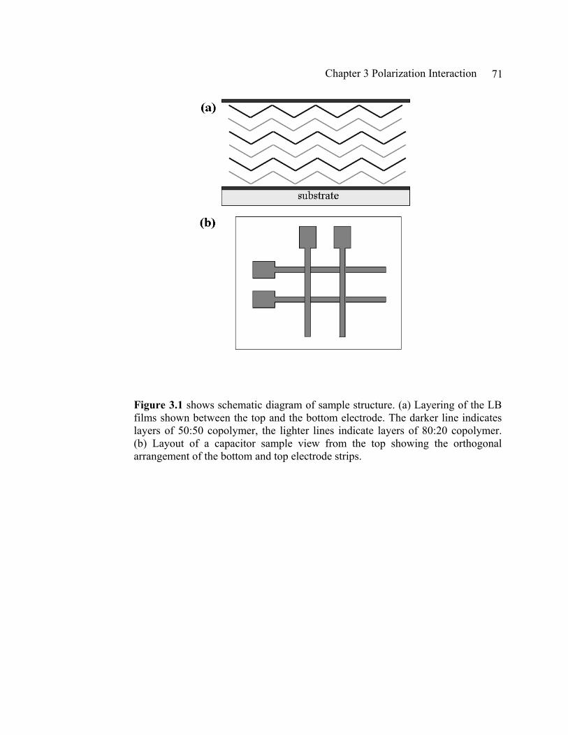
Chapter 3 Polarization Interaction
71
71
Figure 3.1 shows schematic diagram of sample structure. (a) Layering of the LB films shown between the top and the bottom electrode. The darker line indicates layers of 50:50 copolymer, the lighter lines indicate layers of 80:20 copolymer. (b) Layout of a capacitor sample view from the top showing the orthogonal arrangement of the bottom and top electrode strips.
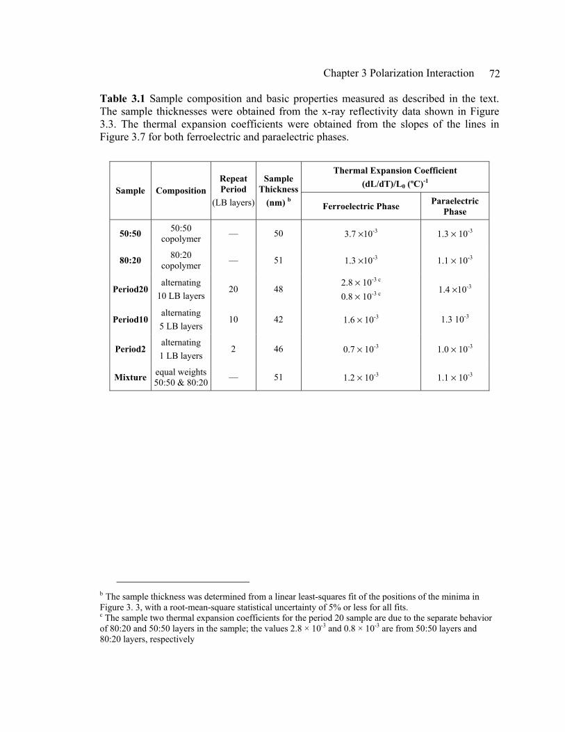
Chapter 3 Polarization Interaction
72
72
Table 3.1 Sample composition and basic properties measured as described in the text. The sample thicknesses were obtained from the x-ray reflectivity data shown in Figure 3.3. The thermal expansion coefficients were obtained from the slopes of the lines in Figure 3.7 for both ferroelectric and paraelectric phases.
Thermal Expansion Coefficient (dL/dT)/L0 (ºC)-1
Sample Composition Repeat Period
(LB layers)
Sample Thickness
(nm) b Ferroelectric Phase Paraelectric Phase
50:50 50:50 copolymer — 50 3.7 ×10⁻³ 1.3 × 10⁻³
80:20 80:20 copolymer — 51 1.3 ×10⁻³ 1.1 × 10⁻³
Period20 alternating
10 LB layers 20 48
2.8 × 10⁻³ c
0.8 × 10⁻³ c 1.4 ×10⁻³
Period10 alternating 5 LB layers
10 42 1.6 × 10⁻³ 1.3 10-3
Period2 alternating 1 LB layers
2 46 0.7 × 10⁻³ 1.0 × 10⁻³
Mixture equal weights 50:50 & 80:20 — 51 1.2 × 10⁻³ 1.1 × 10⁻³
b The sample thickness was determined from a linear least-squares fit of the positions of the minima in Figure 3. 3, with a root-mean-square statistical uncertainty of 5% or less for all fits. c The sample two thermal expansion coefficients for the period 20 sample are due to the separate behavior of 80:20 and 50:50 layers in the sample; the values 2.8 × 10⁻³ and 0.8 × 10⁻³ are from 50:50 layers and 80:20 layers, respectively

Chapter 3 Polarization Interaction
73
73
Three pairs of multilayer samples consisted of equal-thickness alternating layers of the
two copolymers with repeat periods of 2, 10, and 20 LB layers. An additional pair of
samples was made from a solution containing equal amounts by weight of the two
copolymers. The complete list of samples and their compositions is listed in Table 3.1.
3.3 Experimental methods
The breadth of the ferroelectric-paraelectric phase transition and inherent thermal
hysteresis due to phase coexistence make it difficult to determine the true phase transition
temperature. Therefore, we use both dielectric measurements and x-ray diffraction to
investigate the behavior. The advantage of x-ray diffraction is that it provides a
quantitative measure of the amount of material in the ferroelectric and paraelectric states
in the phase coexistence region.47,49,50 As we shall see, this enables us to clearly define an
effective phase transition temperature and also chart the evolution of phase conversion
with temperature and history. Since the x-ray scattering lengths of the two compositions
are almost identical, we were not able to directly probe the multilayer period. However,
as we shall see subsequently, the behavior of the differently structured samples is quite
distinct, implying that the structure of the superlattice is preserved to a large extent.
Sample crystallinity was measured by x-ray diffraction (XRD) in the theta-2theta
geometry, which measures the crystal spacing normal to the substrate. Previous studies
have shown that the LB films have predominately (110) orientation, meaning that the

Chapter 3 Polarization Interaction
74
74
chains, which are along the (001) direction, are in the film plane and the spontaneous
polarization in the ferroelectric phase, which is along the (010) direction is tilted 30°
away from the normal.47,50 The XRD peaks near 18° and 19° at an x-ray wavelength λ=
1.54 Å are the (110) diffraction peaks in the paraelectric and ferroelectric phases,
respectively.51 These peaks have the same structure factor, so the integrated intensities
give the relative fraction of material in each phase.50
Initial x-ray diffraction measurements were performed on a set of preliminary
samples to determine the sample crystallinity and follow the progress of the phase
transition as they were heated. These measurements were made on a Rigaku theta-2theta
diffractometer with a fixed Cu-Kα cathode. This initial XRD measurement showed
relatively low crystallinity of the samples before annealing and considerable
improvement after annealing, as shown in Figure 3.2. For the 50:50 and 80:20 samples
the crystallinity improved by a factor of 5 and 12 respectively as measured by the area
under the diffraction peaks. The samples were annealed by heating them from room
temperature to 135 ºC at a rate of 1 ºC/min, hold it at 135 °C for 2 hours and cool down
to room temperature at the same rate. Both prior studies47,48 and present results indicate
that this annealing procedure optimizes the degree of crystallinity. Each sample was then
enclosed in a temperature-controlled copper chamber, which was mounted on a
goniometer. The chamber operated at atmospheric pressure and had a 9-mm-thick
polyimide window for x-ray access. The sample temperature was accurate within 2 °C.
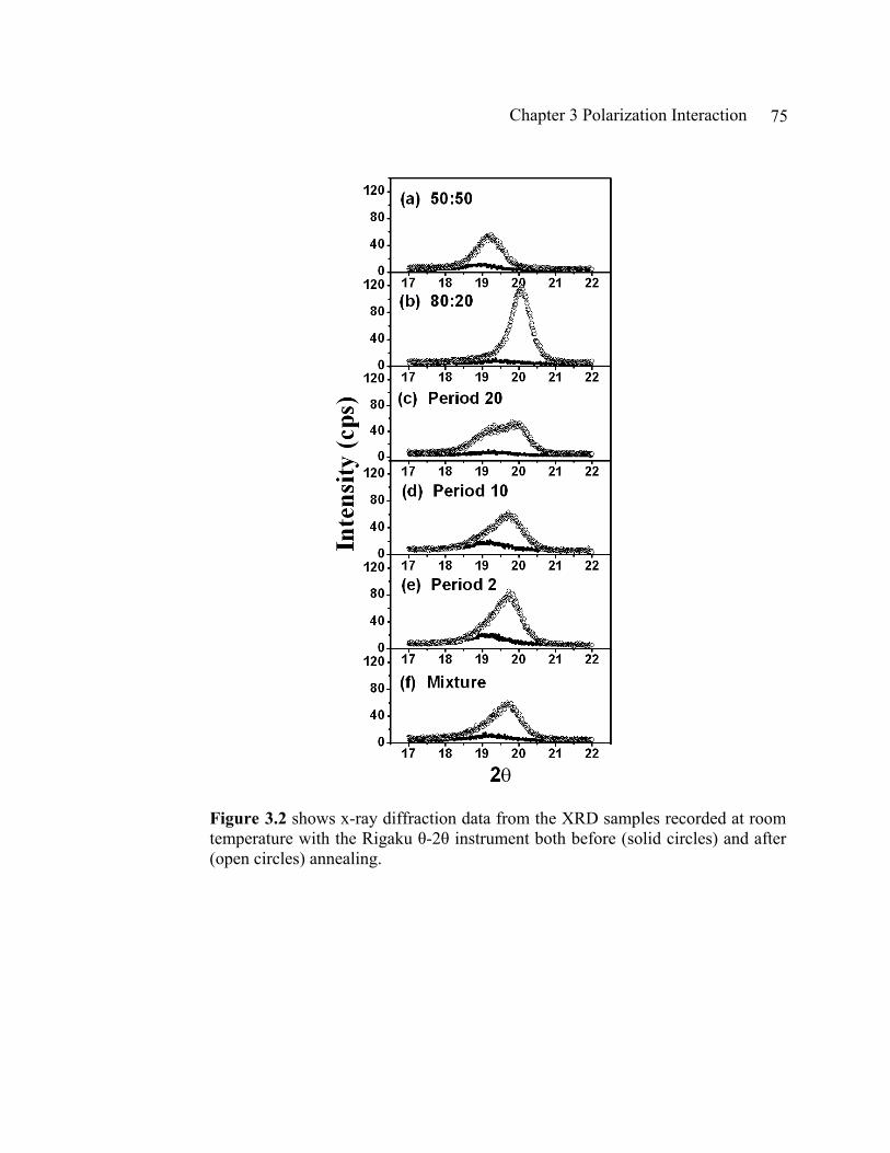
Chapter 3 Polarization Interaction
75
75
Figure 3.2 shows x-ray diffraction data from the XRD samples recorded at room temperature with the Rigaku θ-2θ instrument both before (solid circles) and after (open circles) annealing.

Chapter 3 Polarization Interaction
76
76
The sample temperature was increased at the rate of 1 °C/min. Measurements were made
at intervals of 20° C after holding for 20 min at each set temperature. An identical set of
samples was then made for the detailed XRD studies performed at the synchrotron.
The total thickness of each film was measured after completion of the synchrotron
studies by grazing-incidence theta-2theta x-ray reflectivity on a Bruker AXS
diffractometer. This data was analyzed as follows. The x-ray diffraction intensity was
multiplied by k4, where
θλπ sin2=k (1)
is the scattering vector, in order to account for the effects of the Fresnel reflectivity. The
modified reflectivity data for all 6 samples are shown in Figure 3.3. The presence of
multiple oscillations indicates relatively smooth interfaces. The sample thickness was
determined by using the modified Bragg equation,
22sin2)21( cmtm θθλ −=+ (2)
for the positions of the diffraction minima, where m is an integer index for the diffraction
order, λ is the x-ray wavelength (1.54 Å in this case), t is the film thickness, mθ is the
angle corresponding to the diffraction minimum of index m,52 and Cθ = 0.2º is the critical
angle of the copolymer for x-rays with wavelength 1.54 Å.

Chapter 3 Polarization Interaction
77
77
Figure 3.3 shows X-ray reflectivity data recorded with the Bruker θ-2θ instrument showing thickness oscillations for the indicated samples. The curves have been offset vertically for clarity. All except for the 50:50 sample were the same as those used for the synchrotron x-ray diffraction studies. The original 50:50 sample was unavailable for the x-ray reflectivity studies, so the sample prepared for the primary check-up study before XRD measurement at the synchrotron was used. Due to small number of fringes with this particular sample, an additional sample was also prepared under same condition, and the thicknesses from both samples are the same within experimental uncertainty.

Chapter 3 Polarization Interaction
78
78
The small difference in scattering length densities between the two copolymers implies
that the multilayered samples may be treated as a single uniform layer for the purposes of
this thickness measurement. The thicknesses determined by x-ray reflectivity are listed in
Table 3.1. The sample thicknesses for the pure 80:20 and 50:50 and the mixture
compositions are 50 nm, while the multi-layer samples are slightly thinner, with an
average thickness of 45 nm, slightly thinner than the pure compositions.d According to
these thickness measurements, each transfer of LB film from the water sub-phase consists
of approximately 6 molecular layers per LB transfer. The roughness is estimated to be
approximately 2 nm, as seen from previous AFM measurements on P(VDF-TrFE 70:30)
copolymer films fabricated under the same conditions.53
The bulk of the x-ray diffraction measurements were made at the Advanced
Photon Source at Argonne National Laboratory, on the 12-BM/BESSRC-CAT beam line,
which operated at a wavelength λ = 1.0 Å with an 2θ angular resolution of 0.012°. The
sample was placed in vacuum on the cold finger of a recirculating gas refrigerator that
was mounted on the diffractometer goniometer. The sample temperature was accurate to
within 1 °C. The diffraction measurements were recorded on both heating and cooling
over the range –5 °C to +125 °C, at temperature intervals of 5 °C far from the phase
d In Appendix C, thickness of different 20 LB layers of 80:20 and 50:50 copolymer samples are presented, and the thickness determination was done with a different form of eq.2 is used. The critical angle does not need for the analysis; rather the critical value was obtained from the analysis. Between two studies the determined thickness shows approximately 1 nm discrepancy for both copolymer films.

Chapter 3 Polarization Interaction
79
79
transition temperature, and intervals of 3 °C near it. Beginning the measurements well
below room temperature ensured that the samples were initially in the ferroelectric phase.
The dielectric constant of a ferroelectric exhibits peaks at the transition between
the paraelectric and ferroelectric phases. These peaks are due to the large polarizability
near the phase transition. Capacitance measurements were made with a Hewlett-Packard
4192A Impedance Analyzer operating at a frequency of 1 kHz and an amplitude of 0.1 V.
The samples were mounted in a temperature-controlled copper chamber at atmospheric
pressure. The sample temperature was accurate within 1 °C. The sample capacitance was
continuously recorded as the sample was heated at a rate of 1 °C/min from room
temperature to 125 °C and while cooling back to room temperature at the same rate. The
exception was the pure 80:20 composition sample which was heated to 135 ºC.
The switching behavior of the capacitor samples was characterized at room
temperature by measuring the capacitance as a bias voltage was slowly varied between
opposing polarization saturation levels. The capacitance hysteresis data shown in Figure
3.4 demonstrates that all the samples exhibit the characteristic ‘butterfly’ shape, with
capacitance peaks indicating polarization switching. The butterfly curves repeat on
continued cycling and are typical of those obtained with the ferroelectric copolymer LB
films.43,54 The magnitude of the coercive voltage varies slightly among the samples, but
does not seem to be correlated with the layered structure. This is to be expected, because
the coercive field of the copolymers depends only weakly on composition.55

Chapter 3 Polarization Interaction
80
80
Figure 3.4 shows ‘butterfly’ hysteresis curves of the capacitor samples measured at a frequency of 1 kHz and amplitude 0.1 V while cycling the bias voltage at a rate of 6 V/min.

Chapter 3 Polarization Interaction
81
81
3.4 Results and Discussion
Structure
The ferroelectric-to-paraelectric conversion is accompanied by a change in the
crystal structure from the all-trans conformation of the ferroelectric phase to the trans-
gauche paraelectric phase. Figure 3.2 shows the theta-2theta XRD data from the
synchrotron recorded at the lowest (–5 °C) and highest (+125 °C) temperatures for all the
samples. The peaks near 2θ = 13° correspond to a (110) d spacing of 4.4 Å for the
ferroelectric phase, while the peaks near 2θ = 11.9° correspond to a d spacing of 4.8 Å for
the paraelectric phase. The lattice expansion of 10% from the ferroelectric to paraelectric
phases is due to the increased size of the chains with trans-gauche conformation.51 The
pure 80:20 sample and the Period 20 sample have noticeable amounts of residual
ferroelectric phase at 125 ºC, due to phase coexistence and the relatively high transition
temperature of the 80:20 copolymer, a point that will be discussed further below.
The lattice spacing in the paraelectric phase is only weakly dependent on
composition, as the peak positions of the pure 50:50 and pure 80:20 samples at 125 °C
were nearly identical, at 11.86±0.02° (4.835±0.005 Å) and 11.95±0.02° (4.80±0.01 Å),
respectively, effectively irresolvable because of the peak width of approximately 0.4
degree. The tightly packed ferroelectric phase, on the other hand, is more sensitive to the
presence of the extra fluorine atoms on the hydrogen side of the backbone. At –5 °C, the
peak positions of the pure 50:50 and pure 80:20 samples are readily resolved, at
12.86±0.02° (4.46±0.01 Å) and 13.48±0.02° (4.26±0.005 Å), respectively.

Chapter 3 Polarization Interaction
82
82
X-ray diffraction results
Figure 3.5 shows the temperature evolution of the (110) peaks for the six XRD
samples from 0°C to 125 °C on heating. The transition between the ferroelectric and
paraelectric phases in the VDF copolymers is gradual, owing to the first-order nature of
the transition.56 The breadth of the phase transition is not sensitive to sample defects or
inhomogeneity, as is evident by comparing studies of polymorphous lamellar samples57
with high quality linear-chain crystals of VDF copolymers. 58 Moreover, the phase
transition is highly hysteretic, so that the transition temperatures on heating and cooling
are different. We will focus on the phase changes observed during heating after
stabilization at room temperature or below, because this produces the best repeatability in
the initial phase proportions. The proportion of each phase is readily quantified by the
intensity of the (110) diffraction peaks, the ferroelectric peak at approximately 13° and
the paraelectric peak at approximately 12°. All samples exhibit a large coexistence
region, the range of temperatures where both phases persist. The pure 50:50 sample (see
Figure 3.5a), having the lower transition temperature, shows essentially full conversion to
the paraelectric phase by approximately 80 °C, while the pure 80:20 sample (see Figure
3.5b) is not yet fully converted at 125 °C. These two pure samples provide a useful
reference for comparison. For example, the XRD data from the Period 20 sample
resembles a superposition of the structures of the two component materials, with two
distinct ferroelectric phase XRD peaks recorded at –5 °C and a two-stage transition to the
paraelectric phase.

Chapter 3 Polarization Interaction
83
83
Figure 3.5 shows the synchrotron x-ray diffraction data as function of temperature, showing the ferroelectric-to-paraelectric phase conversion for the following 20 LB layer films: (a) pure 50:50 copolymer; (b) pure 80:20 copolymer; (c) Period 20; (d) Period10; (e) Period 2; and (f) Mixture.

Chapter 3 Polarization Interaction
84
84
Figure 3.6 shows comparison between x-ray diffraction data recorded at the synchrotron at –5 °C (solid lines) and at 125 °C (open circles) for all the samples. The peaks near 12° are the (110) peaks from the paraelectric phase, while the peaks between 13° and 14° are the (110) peaks from the ferroelectric phase.

Chapter 3 Polarization Interaction
85
85
The mixture sample (see Figure 3.5f), the Period 2 sample (Figure 3.5c), and the Period
10 sample (Figure 3.5d) show nearly full conversion to the paraelectric phase by 125 °C.
On the other hand, both the pure 80:20 sample and the Period 20 sample retain some of
the paraelectric phase, even at 125 °C, as is evident in Figure 3.6b and Figure 3.6c,
indicating that the 80:20 layers in the period 20 sample are relatively unperturbed.
To make a more quantitative comparison, we fit each XRD measurement to a set
of peaks with a Gaussian line shape (except for the Period 20 sample, where a Lorentzian
line shape resulted in higher quality fits). With such thin films and inherently broad
diffraction peaks, the fitting results do not necessarily determine unambiguously which
spacings are present. An elementary model calculation of the expected diffraction peak
heights, widths and positions for the multilayer samples (assuming planar interfaces and
perfect lattice coherence through the thickness of the sample) indicates that the (110)
peaks for the ferroelectric structures of the 50:50 and 80:20 copolymers should produce a
single irresolvable peak in the Period 2 sample, whereas in the Period 20 sample, the
separate peaks should be clearly distinguishable. (The peak widths, which are of the order
of 1° in 2θ, are much greater than the 0.012° resolution of the APS diffractometer.) Note
that the model shows that that an apparent merging of the (110) XRD peaks in films with
small repeat periods is purely structural – it does not necessarily indicate that the Period 2
sample, for example, behaves as a composite or mixed sample (though this indeed may
be the case), only that the two peaks are structurally indistinguishable. In all but the
Period 20 sample, the two-peak fits (one peak from the ferroelectric phase and only one

Chapter 3 Polarization Interaction
86
86
from the paraelectric phase) were much better, meaning that distinct ferroelectric peaks
for two independent materials could not be resolved. For the Period 20 sample, we
obtained better fits with three-peaks, one for each ferroelectric peak from the two
compositions and a single combined paraelectric peak. (The paraelectric peaks are at
nearly the same spacing, and so are not resolvable, as we confirmed by attempting to fit
two paraelectric peaks.) The peak positions obtained from this analysis are shown in
Figure 3. 7. We calculated the integrated intensity of each peak as obtained from the
fitting procedure, and normalized the intensity to 1 at each temperature, so that the values
represent the fraction of the ferroelectric and paraelectric phases, respectively. The
normalized intensities obtained in this fashion are shown in Figure 3.8.
The lattice spacings of all samples obtained from the peak positions of the x-ray
diffraction data shown in Figure 3.5 are plotted in Figure 3.7 as a function of temperature.
The thermal expansion coefficients for both the ferroelectric and paraelectric phases of all
samples were obtained and are listed in Table 3.1. Regardless of the values of the
expansion coefficients, the lattice spacing of all the heterogeneous samples is
intermediate between that of the pure 50:50 and pure 80:20 copolymers, for both phases.
In the paraelectric phase, both the spacing and the thermal expansion coefficients of the
samples are within a small range, ~ 1% and ~30%, respectively. In the ferroelectric
phase, the lattice spacings and the thermal expansion coefficients of the samples cover a
wider range, ~5% and ~300%, respectively. The thermal expansion of the ferroelectric
and paraelectric peaks in the Period 10 sample are intermediate between the

Chapter 3 Polarization Interaction
87
87
corresponding values for the two pure copolymers, whereas the Period 2 and the mixture
samples show a thermal expansion that is close to (but even lower than) the thermal
expansion coefficient of the 80:20 sample. If we make the reasonable assumption that the
interlayer interaction is proportional to the numbers of interfaces, it follows that the
interactions between the 80:20 and 50:50 copolymers tend to reduce the thermal
expansion coefficients of both materials. The temperature evolution of each phase is quite
different and this leads to a complex temperature dependence of the lattice spacing in the
heterogeneous samples. To understand the nature of these interactions better, we next
consider the relative proportions of each phase as the samples are heated through the
transition temperature.
The relative proportions of each phase, as obtained from the integrated intensities
of the x-ray peaks, are shown as a function of temperature in Figure 3.8. For the pure
50:50 copolymer sample (see Figure 3.8a), the data clearly shows the gradual conversion
from purely ferroelectric phase (solid circles) at low temperature to purely paraelectric
phase (open circles) at high temperatures. The data from the pure 80:20 sample shows a
much more gradual conversion that is only half completed at the maximum measurement
temperature of 125 °C. The rate of phase conversion differs among the samples. In the
pure copolymer samples (see Figure 3.8a and b, we see that below 80 ºC the conversion
rate of the 50:50 copolymer is greater than the 80:20 copolymer, whereas above 80 ºC the
80:20 copolymer has the greater conversion rate.

Chapter 3 Polarization Interaction
88
88
Figure 3.7 shows lattice spacings determined from the x-ray diffraction peaks shown in Figure 3.5 as a function of temperature, for the following samples: (a) pure 50:50 (solid squares); (b) pure 80:20 (open circles); (c) Period 20 (crosses); (d) Period 10 (solid triangles); (e) Period 2 (open triangles); and (f) Mixture (asterisks). The lines represent linear regression fits to the peak positions yielding the thermal expansion coefficients, which are listed in Table 3.1.

Chapter 3 Polarization Interaction
89
89
Figure 3.8 shows the normalized peak intensity as a function of temperature obtained from analysis of the x-ray diffraction data shown in Figure 3.5. The graphs shown are for the six samples as follows: (a) pure 50:50; (b) pure 80:20; (c) Period 20; (d) Period 10; (e) Period 2; and (f) Mixture. Open circles indicate the paraelectric phase, and solid circles indicate the ferroelectric phase. In the graph (c), the open squares and solid squares indicate the peaks associated with ferroelectric phase of the 50:50 copolymer and the 80:20 copolymer, respectively, as described in the text.

Chapter 3 Polarization Interaction
90
90
The intensity data from the Period 20 sample in Figure 3.8c show independent phase
conversion of the two compositions – the ferroelectric peak corresponding to the 50:50
copolymer spacing tracks the phase conversion rate of the pure 50:50 copolymer films,
and similarly for the peak corresponding to the 80:20 composition. In contrast, the
transition rates of the Period 10, Period 2, and the mixture samples in Figure 3.5c-e are
almost constant over the phase conversion range. This behavior is consistent with an
interaction between the different materials, but it is not definitive evidence, because
averaging the rates of phase conversion can lead to similar behavior. The endpoints of the
phase conversion provide a more useful indicator of the effect of sample structure on the
stability of the ferroelectric state.
With the complex phase conversion and thermal hysteresis phenomena, it is often
not sufficient to identify a single transition temperature. Therefore, we define several
useful critical temperatures as follows. The lower critical temperature T0 is the
temperature at which the paraelectric phase first appears as the sample is heated. The
upper critical temperature T1 is the maximum temperature of the ferroelectric phase.
These critical temperatures were determined by extrapolating the XRD peak intensity
data in Figure 3.8 – T0 by extrapolating the paraelectric peak intensity to zero, and T1 by
extrapolating the ferroelectric peak intensity to zero. The phase crossover temperature
T1/2 is the temperature at which the integrated intensities of the ferroelectric and
paraelectric peaks are equal. The value of T1/2 indicates the effective midpoint of the
phase coexistence region, whether or not the layers are interacting. The critical
Chapter 3 Polarization Interaction
91
91
temperatures of all samples are listed in Table 3.2. The critical temperatures of the pure
50:50 sample determined by this method are T0 = 9±1 °C and T1 = 85±8 ºC. These limits
are clear and unambiguous because the phase coexistence region is relatively narrow and
the phase transition temperature is low. However, the more gradual transition of the
80:20 sample, together with the high value of the phase transition temperature, lead to
more uncertainty in the values of T0 and T1. Even at 125 °C, the sample consists of
approximately 50% ferroelectric phase and 50% paraelectric phase, so that we are not
able to even define a T1 for the 80:20 sample. At the lowest temperature of –5 ºC, the
paraelectric peak is already evident (see Figure 3.5b), and the T0 of the 80:20 copolymer
determined by this extrapolation method ranges between -40 ºC and –30 ºC.
The transition temperatures listed in Table 3.2 indicate that for the Period 10
sample, the value of the lower critical temperature T0 is close to that of the pure 50:50
sample, whereas for the Period 2 and mixture samples, T0 is lower, and in-between that of
the 50:50 and 80:20 copolymers. The value of the upper critical temperature T1 for all
three samples is approximately the same, and well above that for the pure 50:50 sample.
The phase transition region in the multilayer and mixture samples is much wider than for
the pure 50:50 sample, but much narrower than that of the 80:20 sample. The effect of
sample structure on the transition temperature is strong evidence for interlayer
interaction; the ferroelectric-to-paraelectric phase transition in these films is strongly
influenced by the proximity of the 80:20 and 50:50 copolymers, leading to a behavior
intermediate to that of the pure samples.
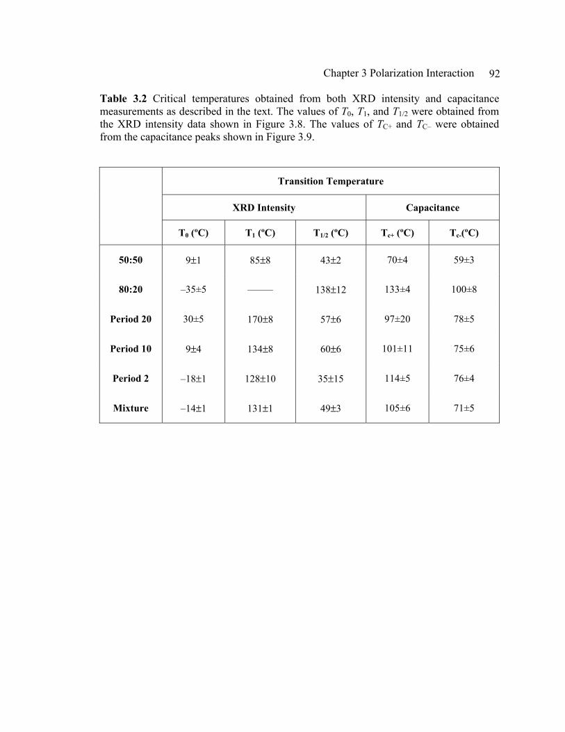
Chapter 3 Polarization Interaction
92
92
Table 3.2 Critical temperatures obtained from both XRD intensity and capacitance measurements as described in the text. The values of T0, T1, and T1/2 were obtained from the XRD intensity data shown in Figure 3.8. The values of TC+ and TC– were obtained from the capacitance peaks shown in Figure 3.9.
Transition Temperature
XRD Intensity Capacitance
T0 (ºC) T1 (ºC) T1/2 (ºC) Tc+ (ºC) Tc-(ºC)
50:50 9±1 85±8 43±2 70±4 59±3
80:20 –35±5 ––––– 138±12 133±4 100±8
Period 20 30±5 170±8 57±6 97±20 78±5
Period 10 9±4 134±8 60±6 101±11 75±6
Period 2 –18±1 128±10 35±15 114±5 76±4
Mixture –14±1 131±1 49±3 105±6 71±5

Chapter 3 Polarization Interaction
93
93
Although we do not have enough quantitative information to extract an exact interaction
length, we see that as the number of interfaces increase in going from the Period 10 to
Period 2 sample, T0 drops quite dramatically.
Capacitance results
Another indicator of the ferroelectric-paraelectric phase transition is the dielectric
anomaly, a peak that occurs at or near the phase transition temperature. Figure 3.9 shows
the dependence of the capacitance on temperature for all samples as they were heated
from room temperature to 125 °C and then cooled back to room temperature, both
directions at a rate of 1 °C/min. Decreasing the heating or cooling rates by a factor of 5
does not significantly affect the results, so we consider these measurements to be made
under quasi-equilibrium conditions.16 The capacitance data for the pure 50:50 sample (see
Figure 3.9a) shows the typical behavior of a ferroelectric polymer, with a peak on heating
indicating the ferroelectric-paraelectric phase transition, and another one on cooling
indicating the paraelectric-ferroelectric phase transition. The heating and cooling curves
show thermal hysteresis, a consequence of the first-order nature of the phase transition.
The temperatures of the heating and cooling peaks in the capacitance, designated as TC+
and TC–, respectively, are listed in Table 3.2. Since the pure 80:20 sample was not fully
converted to the paraelectric phase, its cooling peak (see Figure 3.9b) was broadened.
The cooling peaks are all very similar, with TC– values between those for the pure
samples. Note that the values of T1/2 obtained from XRD are all lower than TC–.

Chapter 3 Polarization Interaction
94
94
Figure 3.9 shows the dependence of capacitance on temperature during heating (solid circles) and cooling (open circles) for six capacitor samples with the following construction: (a) pure 50:50; (b) pure 80:20; (c) Period 20; (d) Period 10; (e) Period 2; and (f) Mixture.

Chapter 3 Polarization Interaction
95
95
The breadth of the transition and the large thermal hysteresis are not very sensitive to
sample crystallinity, 47-50 as is evident by the similar shape of the capacitance-temperature
curves obtained with polymorphous samples,55 LB films,43 and high quality crystals.59
Although the locations of the capacitance peaks in the different samples gives
some indication of interaction between layers of different compositions, the shapes of the
heating peaks are even more revealing. Consider the shapes of the heating peaks for the
multilayer and mixture samples, as shown in Figure 3.9c-f. The Period 20 multilayer
sample shows a broad plateau in the capacitance on heating, whereas the Period 10
sample shows a narrower plateau and the Period 2 and mixture samples show rounded
peaks. The expected dependence of the capacitance on temperature in an ideal non-
interacting sample can be calculated by treating the layers with different compositions as
capacitors connected in series. Applying this idealization to the data in Figure 3.9a and b
yields the dashed line shown in Figure 3.9c. This line would apply to any of the
multilayer structures if the layers are not interacting. The calculation yields a broad
plateau very similar to the one in the data for the Period 20 sample, indicating that the
Period 20 sample behaves as two independent films with little evident interaction
between them, consistent with the above analysis of the x-ray data. (The calculated
capacitance is lower than that measured in the Period 20 sample. Previous measurements
have shown some variation in sample capacitance, probably a result of sample-to-sample
variations in film thickness and electrode coverage.46)
Chapter 3 Polarization Interaction
96
96
The Period 10 sample shows a narrower plateau than expected for a
noninteracting sample (i.e., the dashed line in Figure 3.9c), but not a single peak that
would indicate a sample with a single transition temperature. It is more consistent with an
intermediate situation – a sample consisting of independent, but interacting layers. The
phase transition in part of each layer is influenced by interaction with its neighboring
layers. This has the effect of raising the effective transition temperature of the adjacent
50:50 layers and lowering the effective transition temperature of the adjacent 80:20 layers
and therefore narrowing the plateau compared to that of the noninteracting sample.
The heating peaks of the mixture and Period 2 samples, on the other hand, are
relatively narrow, consistent with a film with a single, phase transition. Furthermore, the
heating peaks for these samples are much closer to that of the pure 80:20 sample and
there is no indication of a peak corresponding to the heating peak of the pure 50:50
sample. The capacitance and x-ray diffraction data from the mixture and Period 2
samples are nearly identical with each other, further supporting the hypothesis that thin
multilayers have such strong interaction that they behave as a single composite sample.
Summary of results and discussion
The results of the x-ray diffraction and dielectric measurements can be
summarized as follows. The Period 20 sample can be considered as two independent
films. The temperature dependences of both the x-ray diffraction and capacitance data are
consistent with two independent layers exhibiting little or no interaction. On the other end

Chapter 3 Polarization Interaction
97
97
of the range, both the Period 2 and mixture samples behave like a composite system with
a single ferroelectric-paraelectric phase diagram. The Period 10 sample, on the other
hand, exhibits both composite behavior and distinct features of 80:20 and 50:50
copolymers. This suggests that the effective interaction length is approximately the
thickness of one of the material layers, or about 11 nm, corresponding to one of the four
distinct material layers of the Period 10 sample.
An alternate explanation for the composite behavior observed with the Period 2
and Period 10 samples is that the layers intermixed in some way, perhaps during LB
deposition or during annealing. Layer mixing during deposition might arise from gaps in
individual layers, but our studies show that individual layers are continuous 60,48,53 and
that films of only 1 or 2 LB layers usually make good capacitors,16,61,62 indicating that
gaps and pinholes are uncommon. The film transfer ratio during constant-pressure
deposition is consistently near 1:1, which rules out significant layer mixing or thickness
variation due to removal of previous layers. The x-ray diffraction measurements at the
annealing temperature show that the samples were never melted, so there was no chance
of mixing in the melt, when the polymer chains are mobile. Also, melted films
recrystallize into needles with completely different orientation, losing their (110)
orientation.48,53 Because of the length and stiffness of the chains, they do not readily
diffuse through each other in the solid state. This process would require highly unlikely
cooperative motions of dozens to hundreds of formula units in multiple chains.

Chapter 3 Polarization Interaction
98
98
To test the sample stability during annealing, and put an upper limit on interlayer
diffusion, we made additional annealing studies on the Period 10 and Period 20 samples
after all the other measurements were completed. Since the initial annealing time was 2
hrs, we subjected the Period 10 and Period 20 samples at 135 °C to two additional
annealing cycles of 20 hrs and one of 200 hrs. (This is in addition to several hours spent
at elevated temperature during the synchrotron studies.) If these long annealing times led
to greater inter-diffusion, we would expect both greatly decreased peak intensities (due to
the larger amount of defects resulting from inter-diffusion) and, in the case of the period
20 sample, a smearing of the two resolvable ferroelectric peaks (see Figure 3.6c). The
two 20 hr and the 200 hr annealing cycles did produce some decrease in the intensity of
the 50:50 x-ray diffraction peak in the Period 20 sample by amounts of 10% after 40 hrs,
to 20% after an additional 200 hrs. Similarly, the Period 10 sample exhibited decreases of
15% and 34% after 40 hrs and 200 hrs, respectively. The positions of the two
ferroelectric peaks from the Period 20 sample were insensitive to the extra annealing, and
both peaks are clearly resolvable even after a total of 240 hours of annealing. These
extended annealing studies shows that even after 100 times longer annealing there is little
or no change in the Period 20 sample, so that is seems very unlikely that the period 10
sample suffered diffusion effects after only two hours of annealing. Taken together, all
the annealing studies allow us to conclude that it is unlikely that the observed composite
behavior is due to inter-diffusion of the 80:20 and 50:50 multilayers.
Chapter 3 Polarization Interaction
99
99
3.5. Conclusions
The capacitance and x-ray diffraction data in the multilayer samples establishes a
progression consistent with an interaction length of approximately 11 nm. (This is larger
than the interaction length of ≤ 4 nm estimated for interactions between the VDF
copolymer and Cu phthalocyanine particles in a nanocomposite.34) The Period 20 sample
shows little or no interaction between the relatively thick films of pure 50:50 and 80:20
copolymer. The Period 10 sample exhibits behavior intermediate between that of
noninteracting films and a composite film. The Period 2 sample behaves as a composite
sample, nearly identical in structure and behavior to that of the mixture sample.
We note that the lower critical temperature, T0, and the higher critical temperature
T1 occur in two different regimes. At and below T0 the samples are all fully ferroelectric.
Hence all the interactions occur between ferroelectric phases of the 50:50 and 80:20
materials. Between T0 and T1, there exists a heterogeneous mixture of ferroelectric and
paraelectric regions. In this regime, one can envisage an interaction driven by the
polarization of the ferroelectric phase on the paraelectric regions, thereby increasing T1
and/or changing the transition rate as compared to the pure samples.
In ferroelectric thin films, there are two general interaction mechanisms –
mechanical and electrostatic. Both are connected with boundary conditions and are most
pronounced in systems with a first-order ferroelectric phase transition. Mechanical
interaction arising from stress is common in epitaxial systems, where the interaction

Chapter 3 Polarization Interaction
100
100
length is the distance over which strain is relaxed, usually through accumulation of
dislocations.12,29 For the VDF copolymers, the lattice constants perpendicular to the
polymer chain are 10% smaller in the ferroelectric phase than in the paraelectric phase.
For example, the compressive stress of an 80:20 layer in its ferroelectric phase, with its
smaller lattice spacing, on a 50:50 layer in its paraelectric phase would tend to stabilize
the ferroelectric phase of the 50:50 material, and raise its transition temperature. This
effect is also observed in high-pressure studies, where the transition temperature of the
VDF copolymers increases linearly with the application of hydrostatic pressure.63
Electrostatic interactions arise from the boundary conditions on the electric
displacement. In a multilayer capacitor containing both ferroelectric and paraelectric
layers, surface charge on the ferroelectric layer produces an electric field in the
paraelectric layer, which in turn tends to polarize the paraelectric layer, stabilizing the
ferroelectric state, and raising the transition temperature of the paraelectric layer. This
effect is also observed in applied-field studies, where the transition temperature of the
VDF copolymers increases linearly with the application an external electric field.50
With either mechanism, mechanical or electrostatic, the phase transition and
critical temperatures for the Period 10, Period 2 and mixture samples can be described as
follows. For the Period 10 sample, the value of T0 = 9±4 ºC. For non interacting layers,
the x-ray peaks should be additive. A simple model in which the experimental intensities
of the pure 80:20 and the pure 50:50 sample as a function of temperature are added

Chapter 3 Polarization Interaction
101
101
together gives an extrapolated T0 value 2.5±3 ºC, which is fairly close to T0 = 9±4 ºC.
This indicates that in the ferroelectric phase, there is little or no interaction in the Period
10 sample. The much lower T0s of the Period 2 and the mixture samples is a strong
indication of the existence of interaction in these samples in the ferroelectric phase. The
Period 10, the Period 2, and the mixture have similar transition rates over the entire
transition region with the peak intensities changing at a rate of approximately
0.008±0.002(ºC)-1. This could be interpreted as evidence that in this mixed paraelectric-
ferroelectric phase region, the interaction has a fairly long length scale and is insensitive
to the shorter period.
In summary, studies of ferroelectric-paraelectric phase transition temperature in
multilayers consisting of ferroelectric VDF copolymers with different compositions, and
therefore different phase transition temperatures, show clear evidence of interaction
between the two copolymers, with an estimated interaction length of 11 nm. The main
evidence for this conclusion is the observation that samples with a layer thickness thicker
than 11 nm exhibit little or no interaction, while thinner samples exhibit interaction and
the thinnest sample exhibits composite behavior nearly identical to a mixture sample. The
transition from independent to interacting to composite behavior has not been reported
before with ferroelectric multilayers. This begins a new approach to the study of
polarization correlations in ferroelectric systems. It also offers new opportunities for
materials engineering afforded by the ability to control the transition temperature and the
breadth of the coexistence region. For example, ferroelectric polymers make a good

Chapter 3 Polarization Interaction
102
102
acoustic match to aqueous environments and are therefore useful for ultrasonic imaging
and for sonar, where the temperature of the environment is nearly constant.

Chapter 3 Polarization Interaction
103
103
References
1 D. R. Tilley, Phase Transitions in Thin Films in Ferroelectric Ceramics (Basel:Birkhäuser, 1993)
2 D. R. Tilley, Finite-Size Effects on Phase Transitions in Ferroelectrics, p. 11-45 (Amsterdan:Gordon and
Breach, 1996)
3 J. F. Scott Physica B 150, 160 (1998)
4 J. F. Scott, Ferroelectric Thin Films Phase Transitions 30, 107 (1991)
5 J. Karasawa et al. Ferroelectrics 12 105 (1996)
6 K. Ishikawa et al. Phys. Rev. B 37, 5852 (1988)
7 S. Schlag et al. Solid State Commun. 91, 993 (1994)
8 M. Tanaka, Y. Makino, Ferro. Lett. 24, 13 (1998)
9 T. Maruyama et al. Appl. Phys. Lett. 73, 3524 (1998)
10 N. Yanase, K. Abe et al, Japan. J. Appl. Phys. 38, 5305 (1999)
11 T. Tybell, C. H. Ahn, and J-M Triscone, Appl. Phys. Lett. 75, 856 (1999)
12 N. A. Pertsev et al. Appl. Phys. Lett. 83, 3356 (2003)
13 V. Nagarajan et al. Appl. Phys. Lett. 84, 5225 (2004)
14 J. Junquera and P. Ghosez, Nature 422, 506 (2003)
15 D. Vanderbilt, Ferroelectrics 301, 9 (2004)
16 A. V. Bune et al. Nature 391, 874 (1998)
17 D. Fong et al. Science 304, 1650 (2004)
18 O. Nakagawara et al. Vacuum 66, 397 (2002)
19 C. Lichtensteiger et al. Phys. Rev. Lett. 94, 047603 (2005)
20 M. Sepliarsky et al. Phys. Rev. B 64, 060101 (2001)
21 M. Sepliarsky et al. J. Appl. Phys. 91, 3165 (2002)
22 S. Li et al. Phil. Mag. B 76, 47 (1997)
23 E. D. Specht et al. Phys. Rev. Lett. 80, 4317 (1998)
Chapter 3 Polarization Interaction
104
104
24 A. Q. Jiang et al. J. Appl. Phys. 93, 1180 (2003)
25 C. H. Ahn et al. Science 303, 488 (2004)
26 M. Dawber et al. Phys. Rev. Lett. 95, 177601 (2005)
27 H. M. Christen et al. Phys. Rev. B 68, 20101 (2003)
28 L-H Ong, J. Osman and D. Tilley Phys. Rev. B 64, 134108 (2002)
29 N. A. Pertsev et al. Phys. Rev. B 61, R825 (2000)
30 H. Kholstedt et al. Mater. Re. Soc. Proc. 695, 161(Boston, Nov. 2001)
31 N. A. Pertsev. et al. Phys. Rev. B 67 054107 (2003)
32 Q. M. Zhang et al. Nature 419, 284 (2002)
33 J. Li Phys. Rev. Lett 90, 217601 (2003)
34 L. Kim et al. Ferroelectrics 50, 219 (2002)
35 Y. Lu Appl. Phys. Lett. 85, 979 (2004)
36 D. O’Neill et al. Appl. Phys. Lett. 77, 1520 (2000)
37 H. Zheng et al. Science 303, 661 (2004)
38 F. D. Morrison et al. Science 4, 114 (2003)
39 Y. Luo et al. Appl. Phys. Lett. 83, 440 (2003)
40 Y. Luo et al. Ferroelectrics 59, 1513 (2003)
41 S. M. Nakhmanson et al. Phys. Rev. B 67, 235406-1 (2003)
42 K. Koga et al. J. Appl. Phys. 67, 965 (1990)
43 S. Ducharme et al. Ferroelectric and Dielectric Thin Films, ed H. S. Nalwa, 545-591(San Diego, CA:
Academic, 2002)
44 A. V. Sorokin et al. Mol. Mater. 6, 61 (1996)
45 A. Sorokin, S. Ducharme, and M. Poulsen J. Appl. Phys. 92, 5977 (2002)
46 M. Bai et al. J. Appl. Phys. 95, 3372 (2004)
47 J. Choi et al. Phys. Rev. B 61, 5760 (2000)

Chapter 3 Polarization Interaction
105
105
48 M. Bai et al. Mater. Re. Soc. Proc. 699, 85(Boston, Nov. 2001)
49 M. Poulsen, Use of an External Electric Field to Convert the Paraelectric Phase to the Ferroelectric Phase
in Ultra-thin Copolymer Films of P(VDF-TrFE) B.S. Thesis University of Nebraska, Lincoln, NE USA
50 M. Poulsen et al Mater. Re. Soc. Proc. 655, 161(Boston, Nov.-Dec. 2000)
51 E. Bellet-Amalric Eur. Phys. J. B 3, 225 (1998)
52 C. Thompson, R. F. Saraf, J. F. Jordan-Sweet Langmuir 13, 7135 (1997)
53 M. Bai, The Structure of Ferroelectric PVDF/TrFE Copolymer Langmuir-Blodgett films PhD
Dissertation University of Nebraska, Lincoln, NE USA
54 S. Ducharme et al. Phys. Rev. B 57, 25 (1998)
55 T. Furukawa Phase. Transit. 18, 143 (1989)
56 J. F. Legrand Ferroelectrics 91, 303 (1989)
57 K. Tashiro, Ferroelectric Polymers, ed H S Nalwa, 66-181 (New York: Dekker, 1995)
58 K. Omote et al. J. Appl. Phys. 81, 2760 (1997)
59 H. Shigashi et al. Japan. J. Appl. Phys. 68, 1824 (1999)
60 S. Ducharme et al. Ferroelectrics 252, 191 (2001)
61 S. Ducharme et al. Phys. Rev. Lett. 84, 175 (2000)
62 V. Fridkin et al. Ferroelectrics 314, 37 (2005)
63 E. Bellet-Amalric et al. Polymer 35, 34 (1994)

Chapter 4 Polarization Switching of Nanomesas
106
Chapter 4 Polarization Switching of Nanomesas
4.1 Introduction
As introduced in earlier chapters, nanomesas are disk-shaped nanostructures with
dimension of 100 nm in diameter and 9 nm in thickness, developed through self-assembly
during annealing. Observation of nanomesa formation presented in section 2.5 revealed
that the active formation of nanomesas from a 1 LB layer film of 70:30 copolymer started
at 60 ºC (see Fig. 2.15) and ended between 120 ºC ~ 135 ºC during annealing. Prior
studies done by Bai et al. characterized the properties of nanomesas formed after
annealing at 125 ºC for 1 hour.1 They probed nanomesas macroscopically through X-ray
diffraction, capacitance vs. temperature measurement (CT), capacitance butterfly curves
(CV), and pyroelectric current measurements.1,2 In their study, XRD peaks of nanomesa
samples showed stronger intensity compared to an annealed 20 LB layer thin film, which
implied good crystalinity of nanomesas. CT measurement on a nanomesa-capacitor of
50:50 copolymer showed the ferroelectric-to-paraelectric (paraelectric-to-ferroelectric)
transition at 63 ºC (50 ºC). CV and pyroelectric current (Ip) measurements on the same
nanomesa-capacitor sample showed polarization switching (Fig. 4.1), and the polarization
reversal occurred at approximately ± 13 ~ 14 V. Observation of the phase transition and
the polarization switching evidently proved the ferroelectricity of nanomesas in average.

Chapter 4 Polarization Switching of Nanomesas
107
Figure 4.1 shows AFM images of nanomesas and their average dimensions, modeled as a thin disk. The plot at the upper right of the figure shows a hysteresis in the pyroelectric current and butterfly curve measured from a nanomesa capacitor film, consisting of nanomesas formed from a 3 LB layer film of P(VDF-TrFE) 70:30 copolymer, and a 4 LB layer of polyethylene with the top and bottom aluminum electrodes. The schematic sample configuration of the nanomesas is shown at the upper left corner of the plot. The figures are reused with permission from Mengjun Bai, Applied Physics Letters, 85, 3528 (2004). Copyright 2004, American Institute of Physics.

Chapter 4 Polarization Switching of Nanomesas
108
In contrast to the previous studies, which probed only the average behavior of
nanomesas, the main goal of this project is to study the electromechanical and switching
properties of individual nanomesas. The fact that nanomesas are disk-shaped and
nanoscale in size could possibly open new paths for designing memory devices out of
them, and other ferroelectric applications. Thus, direct investigation on individual
nanomesas is necessary. To make a direct approach at the nanoscale of the individual
nanomesas, a scanning probe microscopy (SPM) system is the best technique to apply.
There are various different kinds of SPM developed to probe different types of
interaction between the probe and the sample surfaces such as Atomic Force Microscopy
(AFM), Scanning Tunneling Microscopy (STM), Magnetic Force Microscopy (MFM),
and Piezoresponse Force Microscopy (PFM). Among those, PFM is a primary tool for
imaging and characterizing ferroelectric materials at nanoscale;3,4,5,6 therefore, it is highly
suitable for the goal of our study. In addition to PFM, there is an advanced application of
PFM called switching spectroscopy PFM (SS-PFM), used for our study. SS-PFM is a
powerful tool to reveal a local switching property of ferroelectric samples.7,8,9
For this study we have used PFM and SS-PFM facilities at the Center for
Nanophase Materials Sciences (CNMS) at Oak Ridge National Laboratory (ORNL) in
collaboration with Dr. Kalinin et al.. Prior to this nanomesa study, investigation on
copolymer thin films10 already started using the system. The thin film study showed that
we could switch the films of 70:30 copolymer consisting 10 LB layers corresponding to

Chapter 4 Polarization Switching of Nanomesas
109
approximately 18 nm with ± 10 V (Fig. 4.2a), and the boundary of oppositely polarized
sample area revealed grain types of switching unit about 25-50 nm in size (Fig. 4.2b).
Also, well-behaving hysteresis loops were obtained from most of the probed sample area
(Fig. 4.2c).
Inspired from the prior study, we planned to obtain PFM images of oppositely
polarized individual nanomesas and piezoelectric switching hysteresis loops from local
areas within an individual nanomesa with SS-PFM. These results would clearly show
ferroelectric properties of individual nanomesas. In following sections of this chapter,
results that we obtained will be presented in detail after a brief description of sample
preparation.
4.2 Sample Preparation
Nanomesa samples were prepared by annealing thin films of 70:30 copolymer
consisting 1 LB layer at 135 ºC for 2 hours. The heating and cooling rate for the
annealing procedure was 1 ºC/min (The detailed LB film deposition process on the trough
can be found in section 1.3.). The sample substrate used for this study was Si wafer with
crystal orientation (100). For convenient sample grounding, aluminum electrodes were
deposited at the back of the Si substrates where the metal sample holder makes a direct
contact with the samples. The DC resistances of the Al electrodes were initially in a range
of 50 ~ 100 kΩ as the electrodes were deposited, and the resistances were lowered to a
range of 5 ~ 10 KΩ after a day of baking in the oven at 200 ºC.

Chapter 4 Polarization Switching of Nanomesas
110
Figure 4.2 (a) and (b) are PFM images and (c) are piezoresponse hysteresis loops obtained from 10 LB layer film of P(VDF-TrFE 70:30) deposited on HOPG. The figures are reused with permission from B. J. Rodriguez, Applied Physics Letters, 90, 122904 (2007). Copyright 2007 American Institute of Physics.

Chapter 4 Polarization Switching of Nanomesas
111
4.3 Polarization Switching Observation with PFM
In this section firstly principles of PFM scanning will be introduced, and then the
results of PFM study will be presented and discussed.
4.3.1. Principles of PFM Scanning
PFM measurement is an additional measurement to AFM. During AFM
measurement, an external AC field with a frequency ω will be applied to the AFM tip,
coated with conductive material, and then AFM will provide additional images of the
electromechanical response of the sample, which are called amplitude and phase images
of piezoresponse on top of the topographic AFM image. For PFM application, AFM runs
in contact mode so that the oscillating piezoresponse can be separated from the constant
topographic signal using lock-in technique. Now, let us look at this procedure in detail.
Elements for the PFM
The PFM system consists of a commercial AFM system (Vecco MultiMode NS-
IIIA) equipped with additional function generators and lock-in amplifiers, and external
signal generation and data acquisition electronics.8,9,10 Also, a custom-built electrically
shielded sample holder was used for direct tip biasing and to avoid capacitive crosstalk
by bypassing the SPM electronics. The probes used for the study are MikroMasch models
CSC37A, CSC37B, and CSC38A coated with Cr-Au and with nominal spring constants
of 0.35 N/m, 0.30 N/m, and 0.03 N/m, respectively. For temperature control, the Vecco
Chapter 4 Polarization Switching of Nanomesas
112
Multimode NS-IIIA has attachable heating and cooling elements. The temperature range
the system could be held stable within 1 ºC over the range 0 ºC to 135 ºC.
Topographic Image
First of all, in contact mode AFM, the interaction between the tip and the surface
results in the deflection of the cantilever, which thus acts as a force sensor.6 The
topography, the AFM image, is recorded by keeping the relative interaction force
between the tip and the sample surface constant through the entire image. The relative
force is controlled by a set-point voltage of the cantilever position detector, which
corresponds to the degree of the deflection of the cantilever due to the tip-sample
interaction. To keep the deflection constant, the vertical position of the cantilever base
moves according to the topography of the sample surface, providing a topographic image.
For imaging nanomesas, the set-point voltage was an order of one tenth V, which
corresponds to a tip force of an order of 1 nN when the spring constant of the tip is
approximately 0.3 N/m.
Piezoresponse Images
Now, let us look at how the contact mode AFM is applied to PFM imaging (Fig.
4.3a). Ferroelectric materials exhibit piezoelectricity, which is an electromechanical
coupling response.11 The presence of a stress jkX in piezoelectric materials induces a
change in the surface charge density iσ of the material,12,13 and they show the following
linear relationship.

Chapter 4 Polarization Switching of Nanomesas
113
Figure 4.3 (a) is a schematic configuration of the PFM system; this figure is from S. V. Kalinin group website http://nanotransprot.ornl.gov; (b) is an example of a set of PFM images; the topography, the amplitude, and the phase. Figure 4.3a is reused with permission from S. V. Kalinin.

Chapter 4 Polarization Switching of Nanomesas
114
jkdirect
ijki Xd=σ (4.1)
where directijkd is the piezoelectric coefficient of the material. This is called the direct
piezoelectric effect. Conversely, applying an electric field kE to the material causes
strain ijx , expressed as
kconverse
kijij Edx = (4.2)
where conversekijd are the converse piezoelectric coefficients of the material, and this is
called the converse piezoelectric effect.12,13 PFM is based on the detection of bias-
induced surface deformation (strain), the converse piezoelectric effect, and the process is
as follows.
During the contact mode AFM scanning, an external AC voltage of a frequency ω
is applied to the tip by using the function generator. The AC voltage on the tip produces
an AC field in the sample. This electric filed will produce a sample deformation,
)cos(~ ϕω +tAd according to the converse piezoelectric effect if the sample is
piezoelectric5,6,7. Note that the sample must have a counter electrode. In this PFM
scanning, adapted to AFM, the signal, detected as a cantilever position, contains both
topography (the position of the cantilever base) and the piezoresponse )cos( ϕω +tA
(oscillation part of the signal) from the sample. The piezoresponse signal, followed the
same frequency ω of the applied field, thus this piezo part of the signal can be separated
out by using the lock-in amplifier, referenced to ω. The oscillating part of the signal,

Chapter 4 Polarization Switching of Nanomesas
115
sorted out by a lock-in, will be sent to the main control program of the microscope
through auxiliary channels, and be recorded as two complementary PFM images; one as
the amplitude, and the other as the phase. As a matter of fact, a PFM measurement
provides three images in total; the usual AFM topography, plus the amplitude and the
phase of the piezoresponse of the sample (Fig. 4.3b).
4.3.2 Scanning Conditions and Issues in PFM
Before we try to record images of switched nanomesas as our goal, we first
needed to test PFM scanning conditions. In this section, the PFM scanning conditions and
the issues that we faced during test-scans will be discussed before we look into the main
results of the PFM study. Throughout the tests, the morphological modification of
nanomesas was a major issue. It is known that AFM imaging in contact mode can be
destructive when the tip-sample distance is below 1 nm.6 However, the modification in
PFM imaging cannot be attributed entirely to the contact mode AFM. The softness of
nanomesas is another fundamental cause of the morphological modification of nanomesas.
Having theses fundamental issues, we focused to reduce the degree of the modification,
and followings are the effects of scan conditions on nanomesa modification.
1) AC Bias: First of all, the effect of AC bias amplitude on the sample
modification was tested by comparing images recorded with and without AC bias at room
temperature. The test showed strong effect of AC bias (Fig. 4.4). The image recorded
without AC bias (Fig. 4.4a) shows nanomesas almost the same as they were formed.

Chapter 4 Polarization Switching of Nanomesas
116
Figure 4.4 shows topography of nanomesas obtained from PFM scanning; (a) with zero bias at room temperature; (b) with AC voltage of 5 Vp.p. at 650 kHz at room temperature.
Figure 4.5 shows topography images of PFM taken; (a) at room temp with AC bias of 4 Vp.p. at 890 kHz; (b) at 0 ºC with AC bias 5 Vp.p. at 570 kHz.

Chapter 4 Polarization Switching of Nanomesas
117
However the image recorded with AC bias of 5 Vp.p. and 650 kHz shows an extreme
modification (Fig. 4.4b). It seems that nanomesas were dragged by the tip and spread
over the sample surface. We tested scanning with lower bias, however, with lower bias,
it was not clear if we were getting good piezoresponse from nanomesas when it is lower
than 3 Vp.p.. Therefore, we decided to find other compensatory conditions to reduce the
modification maintaining AC bias of in a range of 4~5 Vp.p..
2) Temperature and frequency of AC bias: Lowering the scanning temperature
lessened the morphology modification as the effect is shown in Figure 4.5. The lowest
stable temperature we could reach with the cooling element of the system was 0 ºC; we
had water condensation problem going below 0 ºC. We suspect the reason why lowering
temperature helped to prevent the modification is based on the following assumption. A
temperature increase between the tip and nanomesas may occur during contact mode
scanning, this temperature increase could exacerbates the sample modification according
to the fact that copolymer film flows in paraelectric phase1,2, manifested as film
separation. The active film separation starts at 60 ºC (section 2.5). Therefore, lowering
the scanning temperature could help nanomesas remain in ferroelectric phase and prevent
the possible exacerbation in paraelectric phase of nanomesas. However, this assumption
has not been tested.
3) The frequency and amplitude of the applied bias: Both the frequency and the
amplitude of AC bias were manually tuned by monitoring the line scanning. With

Chapter 4 Polarization Switching of Nanomesas
118
frequency of order of hundreds kHz and amplitude in the rage of 4~5 Vp.p., PFM images
were obtained. The modification was insensitive to the tested frequency and the
amplitude of the AC bias. Note that the PFM study on the thin continuous films of
copolymer used the same bias amplitude 4~5 Vp.p..10
4) The scan angle, lines, size, and rate: The scan angle did not show apparent
influence to the sample modification, but the scan lines, size, and rate showed their
effects on the modification. Their common cause of the modification was due to
repetitive contacts between the tip and nanomesas, which is inevitable in contact mode
imaging. The more the frequent contacts are, the worse the modification is (Fig. 4.6). To
obtain images of reasonable resolution we made scans consisting of 256 or 512 scanning
lines. Having this scan line restriction, the modification problem becomes more serious
when the scan area is smaller than 1 micron. This problem was compensated by
increasing the scan rate. The scan rate was approximately 2 ~ 3 lines per second to obtain
good images from a 1~2 micron size of scan area. (Fig. 4.7)
4.3.3. PFM measurements and results
As mentioned at the beginning of the chapter, the main goal for the project is to
study ferroelectric properties of individual nanomesas. Obtaining piezoresponse from
nanomesas is not sufficient to prove ferroelectric properties of nanomesas.

Chapter 4 Polarization Switching of Nanomesas
119
Figure 4.6 shows three consecutively recorded AFM images over the same sample area; (a) first, (b) second (c) the third scan. The nanomesas indicated with the red and blue arrows show changes in their morphology.
Figure 4.7 shows Topography images recorded during PFM scanning on two different areas in the same sample. Both (a) and (b) were recorded under similar conditions, and then; (a) at the scan rate of 1.6 Hz (1.6 lines/second); (b) at the rate of 2.5 Hz

Chapter 4 Polarization Switching of Nanomesas
120
The property distinguishing ferroelectric materials from other piezoelectric materials is
having switchable spontaneous polarization. Therefore, we should present the switching
properties of individual nanomesas to prove their ferroelectricity.
According to our purpose, we planned to obtain PFM images of oppositely
switched nanomesas by recording images after polarizing them with opposite polarity of
DC voltages as the previous thin film PFM study showed the switching properties of the
thin film (Fig. 4.2a). The results are shown in Figure 4.8. In addition to this switching
property of nanomesas, we have observed some detailed structures within individual
nanomesas shown in Figures 4.9 through 4.12. The focus of the analysis on the detailed
structures was whether they are domains or not.
PFM Results 1: Nanomesa Switching
In Figure 4.8 two sets of PFM images are shown; namely PFM1 and PFM2. These
two sets were obtained from the same sample area with following steps. Firstly, a square
of size 600 nm, was scanned with a DC tip bias at +7 V, and then image set PFM1 was
measured over a larger area, a square of size 1.5 μm. After obtaining image set PFM1, the
same polarizing procedure was repeated on the same area of the sample but with a dc bias
of -7 V, and then the image set PFM2 was recorded.
First, we can notice some degree of modification on nanomesas in these two sets
of PFM images.

Chapter 4 Polarization Switching of Nanomesas
121
Figure 4.8 shows two sets of PFM images recorded over the same region. (a) and (d) show topography, (b) and (c) amplitude, and (c) and (f) phase. A 600 nm square area at the center of the image area, was polarized with + 7 V and −7 V for PFM1 and PFM2, respectively. Some specific features are specially marked with circles and squares and arrows for discussion.

Chapter 4 Polarization Switching of Nanomesas
122
The area, circled with red line (spot1) shows severe modification due to an applied bias
during scanning since this area is at the center of the image where previously scanned
with ± 7 V bias. Topography of nanomesas in this red-circled area shows significant
distortion (see Fig. 4.8a), and the corresponding area in amplitude (Fig. 4.8b) and phase
(Fig. 4.8c) images are not following the topography. The area, circled with white line in
Figure 4.8d is an example of the modification due to repetitive scans compared to the
same area in Figure 4.8a since PFM2 was recorded after PFM1 on the same area. Also,
we can notice in these white-circled areas that there has been a scanning drift between
PFM1 and PFM2; the white-circled area in Fig. 4.8d is lower in y position compared to
the same area in Fig. 4.8a.
Despite the modifications described above, these two sets of PFM images clearly
showed oppositely polarized nanomesas. At the center of Fig. 4.8c and Fig 4.8f, we can
see nanomesas in the positive (dark color) phase and in the negative (bright color) phase,
respectively. We named the dark color phase as the positive phase and the bright color
phase as the negative phasea since they were obtained after polarizing with the positive
and the negative bias, respectively. This piezoresponse of opposite polarities proved that
the individual nanomesas could be switched; therefore they were anticipated to be
ferroelectric. Additionally, we observed nanomesas that contained both the positive and
negative phase within one nanomesa in these set of PFM. Those nanomesas are at the
right edge of the 600 nm square of the polarized area, as indicated with the black arrow.
a This is the relative phase. Determination of the absolute phase was not possible in this measurement.

Chapter 4 Polarization Switching of Nanomesas
123
Figure 4.9 shows a set of PFM, named as PFM3 recorded from the area indicated with a white square in PFM2 of Fig. 4.8. The circled nanomesa is called Mesa3 for discussions.
Figure 4.10 (a) and (c) are the topography and mixed piezoresponse of Mesa3 marked in Figure 4.9; (b) a line scan of topography of Mesa3 indicated with a yellow line in (a); (d) shows a line scan of a mixed piezoresponse of Mesa3 indicated with the yellow line in (c); (c) is the calculated mixed piezoresponse (PR) image using the equation shown in (d).

Chapter 4 Polarization Switching of Nanomesas
124
This led us to question whether nanomesa can contain multiple domains or not. To
investigate this, we recorded another PFM image over the target area, squared with while
line in PFM2, and the image is shown in Figure 4.9, namely PFM3.
PFM Results 2: Domains
To test whether the boundary shown in PFM3 is domain boundary or not we
examined the dimension of the nanomesa, circled with white line and named as Mesa3.
The maximum length across Mesa3 is approximately 250 nm, which is more than twice
the size of the typical nanomesa. The maximum length across the bright phase region in
Mesa3 is approximately 140 nm. (These dimensions are measured from the amplitude
image.) These dimensions suggest Mesa3 may consist of two or more nanomesas. In
other words two nanomesas were merged during annealing or by the tip during scanning.
To make sure this conclusion we did following test.
In general, the amplitude images of PFM show a minimum value at the domain
boundary between two opposite polarization.6,10 To see if the boundary we see in the
amplitude image of PFM3 (Fig. 4.9b) is a true domain boundary, we tested it with the
imaging resolution method. The principle of the imaging method is that the width of the
transition from positive to negative piezoresponse determines the PFM imaging
resolution, 6,10 and the procedure is as follows. We firstly generated the mixed
piezoresponse, )cos( phaseamplitudePR ×= for the PFM image of Mesa3 (Fig. 4.10d),
and then a selected line profile of the mixed piezoresponse across the boundary as
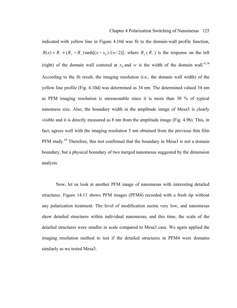
Chapter 4 Polarization Switching of Nanomesas
125
indicated with yellow line in Figure 4.10d was fit to the domain-wall profile function,
)]2//()tanh[()()( 0 wxxRRRxR −−+= −+− , where +R ( −R ) is the response on the left
(right) of the domain wall centered at 0x and w is the width of the domain wall.6,14
According to the fit result, the imaging resolution (i.e., the domain wall width) of the
yellow line profile (Fig. 4.10d) was determined as 34 nm. The determined valued 34 nm
as PFM imaging resolution is unreasonable since it is more than 30 % of typical
nanomesa size. Also, the boundary width in the amplitude image of Mesa3 is clearly
visible and it is directly measured as 8 nm from the amplitude image (Fig. 4.9b). This, in
fact, agrees well with the imaging resolution 5 nm obtained from the previous thin film
PFM study.10 Therefore, this test confirmed that the boundary in Mesa3 is not a domain
boundary, but a physical boundary of two merged nanomesas suggested by the dimension
analysis.
Now, let us look at another PFM image of nanomesas with interesting detailed
structures. Figure 14.11 shows PFM images (PFM4) recorded with a fresh tip without
any polarization treatment. The level of modification seems very low, and nanomesas
show detailed structures within individual nanomesas, and this time, the scale of the
detailed structures were smaller in scale compared to Mesa3 case. We again applied the
imaging resolution method to test if the detailed structures in PFM4 were domains
similarly as we tested Mesa3.
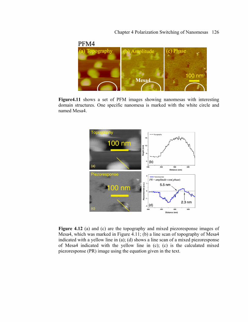
Chapter 4 Polarization Switching of Nanomesas
126
Figure4.11 shows a set of PFM images showing nanomesas with interesting domain structures. One specific nanomesa is marked with the white circle and named Mesa4.
Figure 4.12 (a) and (c) are the topography and mixed piezoresponse images of Mesa4, which was marked in Figure 4.11; (b) a line scan of topography of Mesa4 indicated with a yellow line in (a); (d) shows a line scan of a mixed piezoresponse of Mesa4 indicated with the yellow line in (c); (c) is the calculated mixed piezoresponse (PR) image using the equation given in the text.

Chapter 4 Polarization Switching of Nanomesas
127
First, we magnified the bottom right corner of Figure 14.11 (where the circled nanomesa,
Mesa4 is positioned) and presented the magnified images in Figure 14.12; the topography
(a), the mixed piezoresponse (c), and their line profiles (b) and (d), respectively. The
widths of the domain walls within Mesa4 were determined as approximately 2.3 nm and
5.5 nm as indicated in Figure 4.12d. This value is close to the resolution 5 nm, obtained
from the previous thin film PFM study.10 This convinces us that the imaging resolution
obtained from Mesa4 is real, and therefore, they are domains. As a matter of fact, we can
conclude that nanomesas can contain multiple domains, even though it is not clear at this
point whether the domains were developed during nanomesa formation or during PFM
scanning.
4.4 Polarization Switching Observation with SS-PFM
In the previous PFM study section we have observed that individual nanomesas
are switchable with ± 7 V bias suggesting possible ferroelectricity, and can contain
multiple domains within one nanomesa. Now, in this section a confirmed switching
property of nanomesas, resulted in piezoresponse switching hysteresis loops are
presented. The switching hysteresis loops have been obtained using SS-PFM, and how
SS-PFM records the loops will be introduced first.
4.4.1 Principles of SS-PFM scanning
SS-PFM is an advanced application of PFM. SS-PFM is configured in the force
volume imaging mode. From SS-PFM measurements we can obtain a two dimensional

Chapter 4 Polarization Switching of Nanomesas
128
image map consisting of an array of M × N local piezoelectric switching hysteresis loops
from a scanned area. SS-PFM is configured in force volume imaging mode of Vecco
MultiMode NS-IIIA AFM system.
In the force volume imaging mode, the microscope collects an array of M × N
force curves from a targeted scan area, divided into M × N grids, then the force curves
are mapped out as a two dimensional (2D) image. (The force curve is a function of the
approach-retract travel distance of the tip, recorded as the cantilever deflection according
to the tip-surface interaction force, and the more detailed information about the force
volume imaging can be found in the manual of Vecco MultiMode NS-IIIA and the
website of Vecco).15,16 SS-PFM is developed by adapting this functionality to PFM.
Therefore, we can obtain an array of M × N local piezoelectric switching hysteresis loops
with SS-PFM analogous to the force curves with AFM. For SS-PFM measurement, an
additional function generator (Fig. 4.13d) needs to be added to the PFM system to apply
the switching bias to the scanning tip to obtain piezoelectric switching loops, the
piezoresponse as a function of applied bias (switching bias) at each cell (Fig. 4.13b). The
switching bias is a series of voltage pulses (Fig. 4.13c) that are combined with the small
AC piezoresponse bias (see inset to Fig. 4.13c).

Chapter 4 Polarization Switching of Nanomesas
129
Figure 4.13 (a) shows an array of M×N cells in SS-PFM images; (b) is a schematic plot of a standard switching hysteresis loop; (c) shows the waveform of voltage pulses used for SS-PFM scanning; (d) is a schematic configuration of SS-PFM system. The figures are reused with permission from S. Jesse, Review of Scientific Instruments, 77, 073702 (2006) and Applied Physics Letters, 88, 061908 (2006). Copyright 2006, American Institute of Physics.

Chapter 4 Polarization Switching of Nanomesas
130
Now, let us look at how SS-PFM works in detail. During SS-PFM scanning, the
tip moves from one point to the next in a step motion according to the scan conditions: a
step size l, a number of steps, M (in x direction) and N (in y direction), and a scan rate,
the time taken at each cell. Thus, the entire image consists of M × N small areas of size
l×l so called a cell. At each cell, the series of voltage pulses (Fig. 4.13c) are applied in
sequence, each followed by a piezo measurement, and thus local hysteresis loops are
obtained. The pulse polarizes the local area when it is on for an order of few milliseconds,
and then the piezoresponse from the local area is recorded when the pulse is off. A
number of hysteresis loops can be repeatedly taken at one location, however too many
repeats will increase the total scanning time enormously since a typical SS-PFM
measurement consists of an order of thousand cells. Typically 2 cycles of hysteresis loops
were recorded at each cell. The obtained hysteresis loops from each cell are analyzed
during scanning by fitting to a standard hysteresis loop shape as follows.
The fitting software firstly calculates the average of the 2 cycles of hysteresis, and
the averaged switching loop is fit with the Boltzmann sigma functions (Eq. 4.3 and 4.4)
which represents the standard shape of hysteresis loops.8
6
1
5
321 )exp(1)( Va
aaV
aaVR +⎥⎦
⎤⎢⎣
⎡ −+−=
−+ (4.3)
6
1
5
421 )exp(1)( Va
aaVaaVR +⎥
⎦
⎤⎢⎣
⎡ −+−=
−− (4.4)

Chapter 4 Polarization Switching of Nanomesas
131
)(VR + and )(VR − in above equations are piezoresponse as a function of bias in
forwarding direction (from negative to positive bias, +) and in the reverse direction (from
positive to negative bias, −), respectively. By using the six fitted coefficients 1a ~ 6a in
the fitting function, 9 characteristic parameters of the switching loop (Fig. 4.14a) are
determined for each cell, and then mapped out for the entire scan area (Figure 4.14b). The
characteristic parameters are the initial piezoresponse iniR , the coercive biases 4aV =+
and 3aV =− , the saturation responses 1aRs =+ and 21 aaRs −=− , the switchable
polarization 2aRs = , the imprint 2/)(Im 43 aa += , the slope of the loop 6a , and the
work of switching 2/)( 342 aaaAs −= . This curve fit processing software was developed
by Jesse et al.. The SS-PFM method and the fitting procedure can be found in detail in
their papers.8,9
4.4.2 Scanning conditions and Issues in SS-PFM
Now let us look at the scanning conditions and issues in switching spectroscopy
PFM (SS-PFM). Similar to PFM, SS-PFM showed morphological modification on
nanomesas. As shown in Figure 4.15, nanomesas were significantly distorted after a SS-
PFM scan. In this scan the amplitude of the AC bias was 4 Vp.p., and the maximum DC
pulse for to the switching loop measurement was 10 Vdc. Since we have already observed
that the degree of modification is strongly affected by an applied bias in PFM
measurements (see section 4.3.2), we lowered both the amplitude of AC bias and the
maximum value for the DC pulse to 1~2 Vp.p. and 7~7.5 Vp.p, respectively.

Chapter 4 Polarization Switching of Nanomesas
132
Figure 4.14 (a) is s schematic switching hysteresis loop, labeled with the switching characteristic parameters; (b) is a set of SS-PFM images, consisting of 9 maps. Each map shows the indicated property of the sample surfaces, probed with SS-PFM probe. The figures are reused with permission from S. Jesse, Review of Scientific Instruments, 77, 073702 (2006) and S. Jesse, Applied Physics Letters, 88, 061908 (2006). Copyright 2006, American Institute of Physics.
Figure 4.15 shows topography images obtained from PFM scanning (a) before (b) after SS-PFM scanning.

Chapter 4 Polarization Switching of Nanomesas
133
With the lowered bias, we were able to improve the modification problem involved in
SS-PFM, and these values were used for all results SS-PFM measurements presented in
this dissertation.
Other scanning conditions we checked were the total number of cells (M×N), the
size of the cells and scan area, and the number of steps of switching bias pulses for one
cycle of a switching loop. These conditions were related to the resolution of the image
map, and the scanning time of SS-PFM. Assigning more cells to a scan could give us
higher resolution of image maps in principle; however, the tip drift problem became
significant as the increased cells resulted in a longer scanning time. For example, we
observed 7 % of drift in one direction after a 40-min SS-PFM scan; therefore, we needed
to choose cell numbers considering both the image map resolution, and the total scanning
time. The typical values of the scan conditions that we used are as follows; the total
number of cells is 900 ~1600, the size of cells 12~15 nm, the scanned area ~500 nm2, the
number of pulse steps is 48, and the typical number of cycles of the hysteresis loops at
each cell is 2. It takes approximately a few seconds to complete two switching loops
with 48 switching bias steps in a loop, thus approximately 0.5 ~1 hour for a scan
consisting 30×30 cells.
4.4.3 SS-PFM Results and Discussion
In the PFM study section (section 4.3), we have observed that the piezoresponse
of individual nanomesas is switchable, indicating that they are ferroelectric. In this
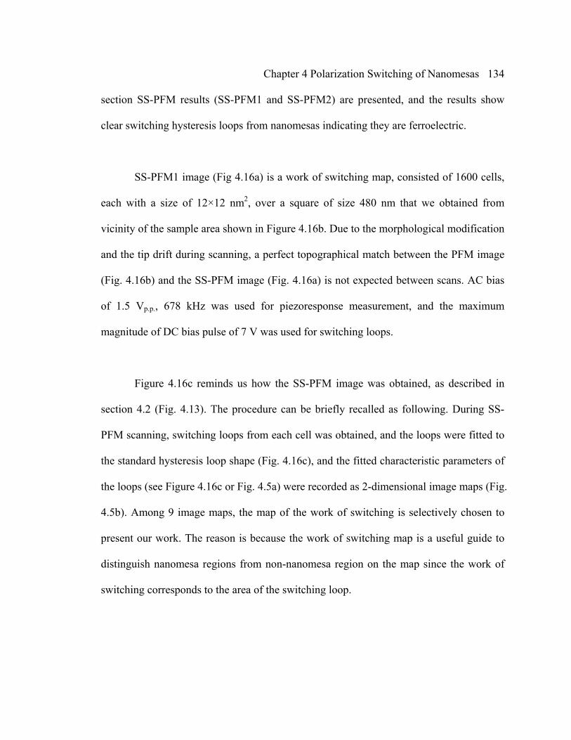
Chapter 4 Polarization Switching of Nanomesas
134
section SS-PFM results (SS-PFM1 and SS-PFM2) are presented, and the results show
clear switching hysteresis loops from nanomesas indicating they are ferroelectric.
SS-PFM1 image (Fig 4.16a) is a work of switching map, consisted of 1600 cells,
each with a size of 12×12 nm2, over a square of size 480 nm that we obtained from
vicinity of the sample area shown in Figure 4.16b. Due to the morphological modification
and the tip drift during scanning, a perfect topographical match between the PFM image
(Fig. 4.16b) and the SS-PFM image (Fig. 4.16a) is not expected between scans. AC bias
of 1.5 Vp.p., 678 kHz was used for piezoresponse measurement, and the maximum
magnitude of DC bias pulse of 7 V was used for switching loops.
Figure 4.16c reminds us how the SS-PFM image was obtained, as described in
section 4.2 (Fig. 4.13). The procedure can be briefly recalled as following. During SS-
PFM scanning, switching loops from each cell was obtained, and the loops were fitted to
the standard hysteresis loop shape (Fig. 4.16c), and the fitted characteristic parameters of
the loops (see Figure 4.16c or Fig. 4.5a) were recorded as 2-dimensional image maps (Fig.
4.5b). Among 9 image maps, the map of the work of switching is selectively chosen to
present our work. The reason is because the work of switching map is a useful guide to
distinguish nanomesa regions from non-nanomesa region on the map since the work of
switching corresponds to the area of the switching loop.

Chapter 4 Polarization Switching of Nanomesas
135
Figure 4.16 shows: (a) a work of switching map obtained from SS-PFM1; (b) a PFM image recorded before SS-PFM1; (c) schematic plots of DC bias pulses, data array of SS-PFM, and a switching loop; (d) a simplified form of the work of switching map in (a); (e) examples of bad fitting results on null hysteresis loops. The size of the cell is 12×12 nm2, the total number of cells 1600. Figure 4.16c is reused with permission from S. Jesse, Review of Scientific Instruments, 77, 073702 (2006) and S. Jesse, Applied Physics Letters, 88, 061908 (2006). Copyright 2006, American Institute of Physics.
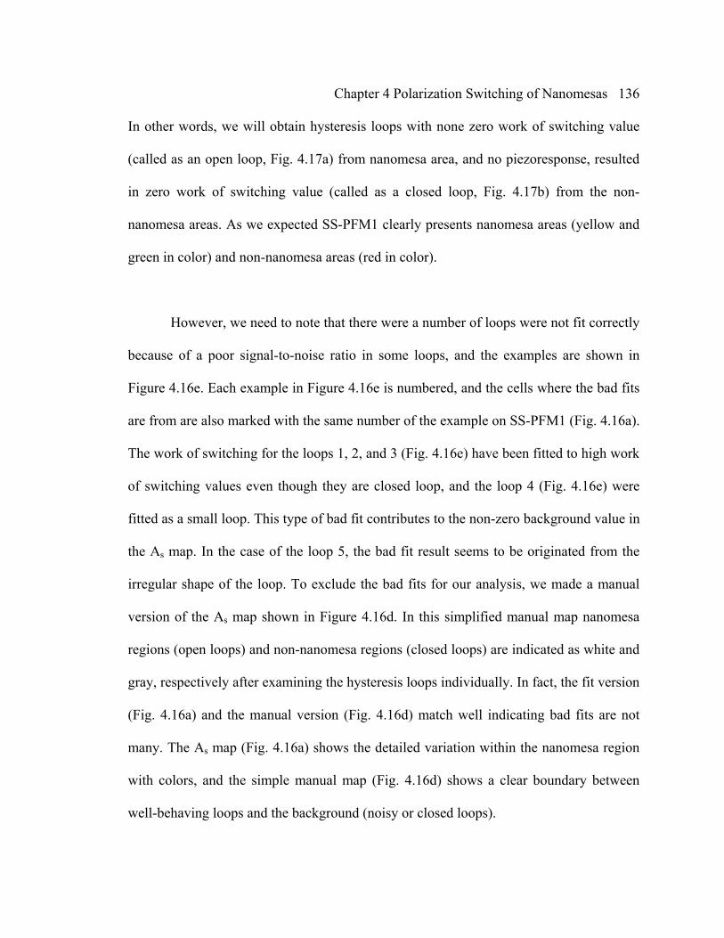
Chapter 4 Polarization Switching of Nanomesas
136
In other words, we will obtain hysteresis loops with none zero work of switching value
(called as an open loop, Fig. 4.17a) from nanomesa area, and no piezoresponse, resulted
in zero work of switching value (called as a closed loop, Fig. 4.17b) from the non-
nanomesa areas. As we expected SS-PFM1 clearly presents nanomesa areas (yellow and
green in color) and non-nanomesa areas (red in color).
However, we need to note that there were a number of loops were not fit correctly
because of a poor signal-to-noise ratio in some loops, and the examples are shown in
Figure 4.16e. Each example in Figure 4.16e is numbered, and the cells where the bad fits
are from are also marked with the same number of the example on SS-PFM1 (Fig. 4.16a).
The work of switching for the loops 1, 2, and 3 (Fig. 4.16e) have been fitted to high work
of switching values even though they are closed loop, and the loop 4 (Fig. 4.16e) were
fitted as a small loop. This type of bad fit contributes to the non-zero background value in
the As map. In the case of the loop 5, the bad fit result seems to be originated from the
irregular shape of the loop. To exclude the bad fits for our analysis, we made a manual
version of the As map shown in Figure 4.16d. In this simplified manual map nanomesa
regions (open loops) and non-nanomesa regions (closed loops) are indicated as white and
gray, respectively after examining the hysteresis loops individually. In fact, the fit version
(Fig. 4.16a) and the manual version (Fig. 4.16d) match well indicating bad fits are not
many. The As map (Fig. 4.16a) shows the detailed variation within the nanomesa region
with colors, and the simple manual map (Fig. 4.16d) shows a clear boundary between
well-behaving loops and the background (noisy or closed loops).

Chapter 4 Polarization Switching of Nanomesas
137
Figure 4.17 shows individual hysteresis loops from indicated area on the work of switching map shown in Figure 4.16 (a) and (d); (a) from the cells, marked with solid circles; (b) from the cells, marked with hollow circles. One cycle of switching loop is consist of 48 pulses and one cycle takes about 1.2 sec
Now let us look at the actual hysteresis loops from the As map. The examples of
switching loops are presented in Figure 4.17. The loops shown in Figure 4.17a are from
the nanomesa region, indicated with solid circles at the bottom right corner on the As
map (Fig 4.16a and d). The loops shown in Figure 4.17b are from non-nanomesa region,
indicated with hollow circles near the center of the bottom on Fig 4.16a and d. One can
notice the clear contrast between them. The well-behaved loops show a gradual decrease
in the work of switching value towards to the center of the nanomesa (towards the left
corner on the map, Fig. 4. 16a and d) as labeled in Figure 4.17a. However, whether this is
from intrinsic properties of nanomesas or from scanning effects, or both, is not clear at
this point. Further investigation is needed to clarify it. Well-behaved loops similar to the
ones presented in Figure 4.17a can be found from areas in green color scale on the As
map. The average coercive voltage for the well-behaved loops is approximately 4 V, and

Chapter 4 Polarization Switching of Nanomesas
138
the average height of the nanomesas after modification are ranged between 9~15 nm.
From this, the determined coercive field is approximately 250 ~ 450 MV/cm. A 10 LB
layer continuous PVDF copolymer film of on graphite film studied with the same SS-
PFM system showed the coercive field was approximately 250 MV/cm,10 which shows
good agreement with our results. The thickness of the 10 LB layer continuous film is
approximately 18 nm.
Another set of PFM and SS-PFM measurements recorded from a fresh spot of the
same sample with which SS-PFM1 was obtained, and they are presented in Fig 18 to 21.
Two sets of PFM images namely PFM 5 and PFM6, respectively (Fig. 4.18) are images
recorded before and after the SS-PFM measurement namely SS-PFM2. The work of
switching map obtained from SS-PFM2 is shown in Figure 4.19. PFM5, the circled area
of PFM6 and the As map of SS-PFM2 show a fair topographic match to one another. The
cell size of SS-PFM2 is 15×15 nm2, and the scanned area is a square of 450 nm.
Examples of well-behaving switching loops and closed loops from SS-PFM2 are shown
in Figure 4.20 in a similar fashion as described for SS-PFM1. These loops from SS-
PFM2 seem qualitatively consistent with the previous ones from SS-PFM1.
Now, let us note some interesting points. In this set of SS-PFM measurements we
have observed the vertical reflection of the hysteresis loops (see Fig. 4.20a and b). This is
likely due to the phase shift of the AFM probe, which often happened when the driving
frequency is closer to the cantilever resonant frequency or its harmonics.9

Chapter 4 Polarization Switching of Nanomesas
139
Figure 4.18 shows two sets of PFM, named as PFM5 and PFM6. PFM5 and PFM6 were scanned, respectively before and after SS-PFM2 shown in Figure 4.19. The area, circled in the phase image of PFM6 shows a fair matching with SS-PFM2.
Figure 4.19 shows; (a) a work of switching (As) map obtained from SS-PFM2; (b) a simplified form of work of switching map in (a) The size of the cell is 15×15 nm2, the total number of cells 900.

Chapter 4 Polarization Switching of Nanomesas
140
Figure 4.20 shows switching loops from the indicated area in Figure 4.19 (a) and (b). One cycle of switching loop consists of 48 pulses and one cycle takes about 1.2 sec, and the maximum bias in this loops are ± 7.5 V.
Also, various types of switching loops (Fig. 4.21) have been recorded from the sample
area, numbered as 1 through 9 in Figure 4.19. The differences in the shapes of these loops
shown in Figure 4.21 are very clear and significant in the degree even though they are
next to one another merely with the cell size 15 nm. This phenomenon is considered to be
originated from a significant modification of that region and the corresponding, modified
nanomesa on the top part of the circled area in PFM6 (Fig. 4.18) supports this
consideration. Therefore, based on this we can draw a conclusion that the morphological
modification complicates the switching properties of the nanomesas, also in that modified
region, an instrumental phase shift can occur. The phase shift problem should not be
totally ignored and needs careful observation in the future, even though we strongly
suspect that it is mainly an instrumental effect.
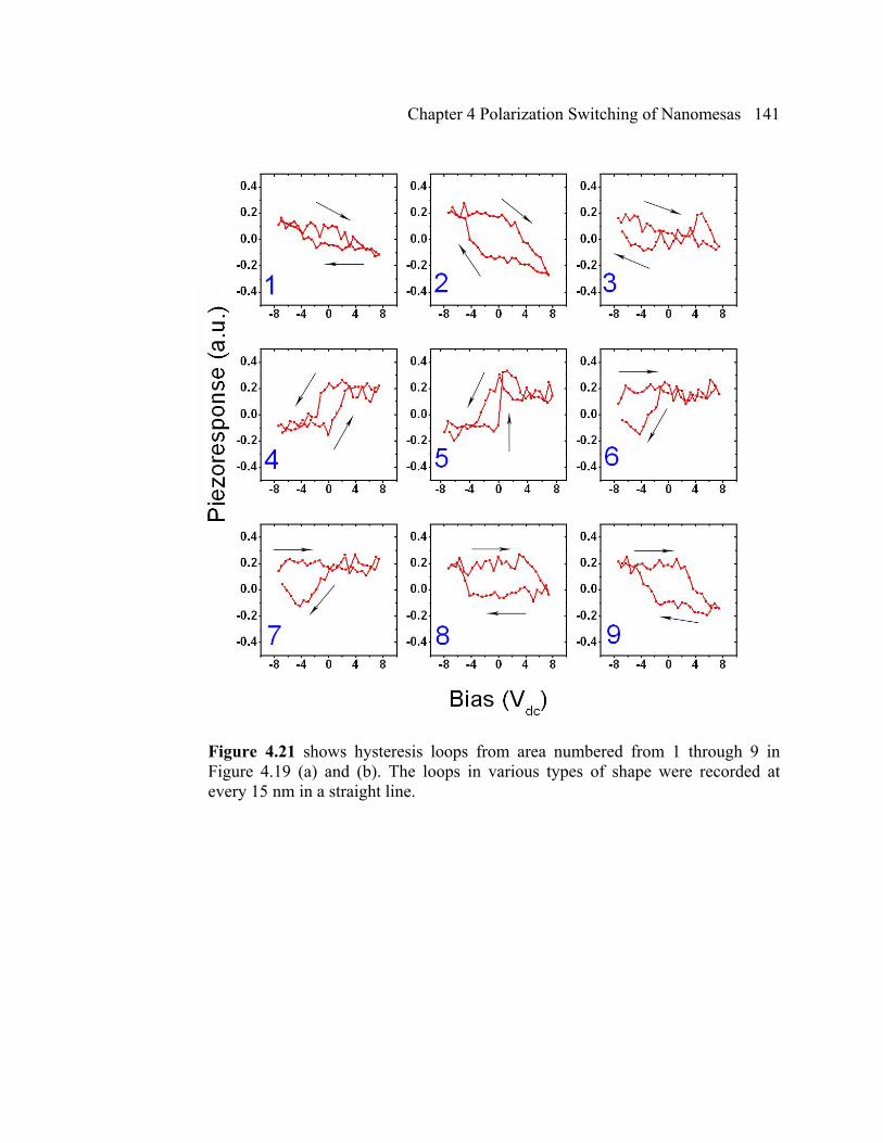
Chapter 4 Polarization Switching of Nanomesas
141
Figure 4.21 shows hysteresis loops from area numbered from 1 through 9 in Figure 4.19 (a) and (b). The loops in various types of shape were recorded at every 15 nm in a straight line.

Chapter 4 Polarization Switching of Nanomesas
142
4.5 Conclusion and Discussion
To conclude this PFM and SS-PFM study of polarization switching of nanomesas,
we firstly observed suggesting switching property of individual nanomesas by recording
PFM images of individual nanomesas, switched in opposite polarities with a dc bias of ±
7 V. Then, we proved the ferroelectricity of individual nanomesas by obtaining well
behaving switching hysteresis loops with SS-PFM from a local area within individual
nanomesas as small as 12 ~ 15 nm. The switching loops are clear evident for
ferroelectricity. The measured coercive field from the well behaving switching loops is
250 ~ 450 MV/m, which shows good agreement to the continuous copolymer films.10
However, throughout the study, we experienced the morphological modification
problem of nanomesas during PFM and SS-PFM scanning, and it has remained as an area
needs to be investigated in the future. Also, the dynamics of switching loops have not
checked in this study. Therefore, in the near future, following investigations can be
attempted. For PFM, we can first try to obtain PFM images of nanomesas, less invaded
either by conducting PFM at lower than 0 ºC or by designing new samples. In the case for
the designing new samples, the goal should be lowering the roughness of nanomesa
sample surface. Reducing the thickness of nanomesas can be considered, however, it
needs to be concerned about how much degree of piezoresponse we would obtain from
nanomesas with the reduced thickness. Alternatively, we could find a way to prepare
substrates with pockets where nanomesas could sit on could or non-piezoelectric
materials, workable with LB technique which can be deposited as capping layers to cover

Chapter 4 Polarization Switching of Nanomesas
143
and protect the nanomesas to make smoother sample surface. In the case of depositing
capping layers on the top of nanomesas, it would not be a direct measurement of
nanomesas, this will be less invasive method. For SS-PFM we can obtain switching loops
from a fixed area within an individual nanomesa, and apply different length of pulses in
time and investigate the switching dynamics of individual nanomesas.

Chapter 4 Polarization Switching of Nanomesas
144
References 1 M. Bai and S. Ducharme, Appl. Phys. Lett. 85 3628 (2004)
2 M. Bai, M. Poulsen, and S. Ducharme, J. Phys. Condes. Matter 18 7383 (2006)
3 G. Zavala, et al. J. Appl. Phys. 81, 7480 (1997)
4 S. V. Kalinin, and A. A. Bonnell in Nanoscale characterization of Ferroelectric Materials, (M. Alexe and
M. Gruverman eds, Springer,2004)
5 S. V. Kalinin, et al. J. Am. Ceram. Soc. 88, 1077 (2005)
6 B. J. Rodriguez, et al. Phys. Rev. Lett. 96, 237602 (2006)
7 S. Jesse et al. Nanotechnology 17, 1615 (2006)
8 S. Jesse et al. Rev. Sci. Instrum. 77, 073702 (2006)
9 S. Jesse et al. Appl. Phys. Lett. 88, 061908 (2006)
10 B. J. Rodriguez et al. Appl. Phys. Lett. 90, 122904 (2007)
11 Kwan Chi Kao Dielectric phenomena in Solids (Elsevier, Inc, 2004)
12 W. G. Cady, Piezoelectricity (Dover Publications Inc., New York, 1964)
13 C. Harnagea, and A. Pignolet in Nanoscale characterization of Ferroelectric Materials, (M. Alexe and M.
Gruverman eds, Springer,2004)
14 M. Bode, Rep. Prog. Phys. 66, 523 (2003): A. Hubert and R. Schäfer, Magnetic Domains (Springer,
Berlin, 1998)
15 F. M. Serry ‘Applications of Force Volume Imaging with Atomic Force Microscopes’ (Veeco
Instruments Inc. http://www.veeco.com , 2004)
16 The manual of the MultiMode NS-IIIA.

Appendix A
145
Appendix A Initial Work for Near Field PSM
Pyroelectric Scanning Microscopy (PSM) has been developed by Dr. Ducharme
et al. in our lab. PSM system recently reached 500 nm of imaging resolution1, and it is
anticipated to have better resolution by introducing the near field effect to the system.
The imaging resolution 500 nm is an effective demonstration resolution estimated by the
minimum size of the distinguishable feature in PSM images. Before presenting the results
of the near field effect simulation and some experimental trials, let us look at the
background of the PSM system.
Background
PSM records the pyroelectric current, originated from the electric polarization of
the sample (see Chapter 2, p. 31),2,3 from a unique x-y position in the sample area using a
focused laser beam and a computer-controlled positioning system.4,5,6 An example of a
pyroelectric switching current loop has been introduced in chapter 2, which uses the same
measurement technique as one implemented to the PSM system. With this technique,
originally attributed to Chynoweth 7 , the pyroelectric current was measured by
illuminating a sample area with a modulated He-Ne laser beam with an optical chopper at
2 kHz rate (see page cahpter2, p32). The modulated laser beam changes the temperature
of the illuminated sample area by heating and cooling at a constant rate. The size of the
illuminated sample area depends on the beam size of the laser, and the heating and
cooling rate depends on the laser modulation frequency, and power of the laser.4 The He-
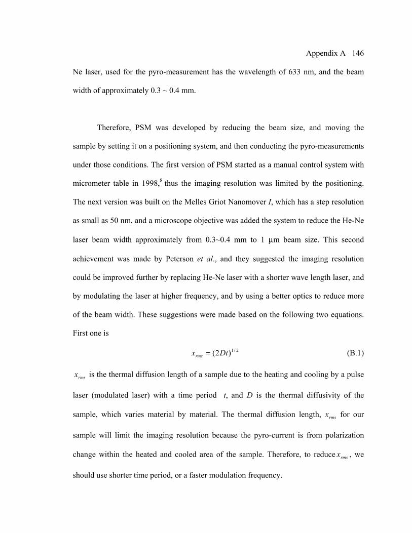
Appendix A
146
Ne laser, used for the pyro-measurement has the wavelength of 633 nm, and the beam
width of approximately 0.3 ~ 0.4 mm.
Therefore, PSM was developed by reducing the beam size, and moving the
sample by setting it on a positioning system, and then conducting the pyro-measurements
under those conditions. The first version of PSM started as a manual control system with
micrometer table in 1998,8 thus the imaging resolution was limited by the positioning.
The next version was built on the Melles Griot Nanomover I, which has a step resolution
as small as 50 nm, and a microscope objective was added the system to reduce the He-Ne
laser beam width approximately from 0.3~0.4 mm to 1 μm beam size. This second
achievement was made by Peterson et al., and they suggested the imaging resolution
could be improved further by replacing He-Ne laser with a shorter wave length laser, and
by modulating the laser at higher frequency, and by using a better optics to reduce more
of the beam width. These suggestions were made based on the following two equations.
First one is
2/1)2( Dtxrms = (B.1)
rmsx is the thermal diffusion length of a sample due to the heating and cooling by a pulse
laser (modulated laser) with a time period t, and D is the thermal diffusivity of the
sample, which varies material by material. The thermal diffusion length, rmsx for our
sample will limit the imaging resolution because the pyro-current is from polarization
change within the heated and cooled area of the sample. Therefore, to reduce rmsx , we
should use shorter time period, or a faster modulation frequency.

Appendix A
147
Figure B.1 (a) is a PSM image over 4×4 (mm)2 area with 1 μm steps recorded with the PSM version2; (b) and (c) are PSM image obtained with the recently developed version3 with a blue diode laser. (b) was recorded with 1 μm steps, and (c) was recorded with 200 nm steps. Figure B.1 (a) is reused with permission from Bradley Peterson, Pyroelectric Imaging in Ultrathin Ferroelectric Films of P(VDF-TrFE), B.A. Thesis, University of Nebraska, Lincoln (2003).

Appendix A
148
The second equation is for the width of the laser focal spot
f
wNA
NAw
2,
20==
πλ (B.2)
The original beam width w0 of the laser can be reduced to w, if we let the beam pass
through a microscope object with a numerical aperture NA. The greater the NA is, the
greater the decrease of the beam width, and shorter wavelength will reduce w.
The recent version of PSM has been developed according to these suggestions.
The new PSM system consists of a blue diode laser (λ = 405 nm), which is capable of
direct modulation up to 5 MHz, and an optical lens system with numerical aperture (NA)
0.85 (see Fig. B.1). The new optical components improved the theoretical resolution from
1 μm to 250 nm. Even though it is an enough resolution for characterizing a large area of
thin film capacitors (a square of 1~3 mm), to probe nanometer scale structures such as
nanomesas, higher resolution is required. Also, further improving of imaging resolution
will make PSM comparable to other scanning probe system such as PFM, and SS-PFM
which have become important nanoscale research techniques for ferroelectric materials.
Moreover, PSM is a very non-invasive scanning system, even compared to PFM which
uses a sharp tip in contact with the sample during scanning.
Near Field Effect
Another means of achieving improved PSM resolution is to use a near-field effect.
We propose to implement a PSM system employing a commercialized scanning
tunneling microscopy (STM) where near-field illumination is afforded by scattering the

Appendix A
149
laser beam from the STM tip. The laser beam scattered off of the very sharp STM tip will
produce enhanced near-field illumination in a subwavelength region in the proximity of
the tip.9,10,11 The simplified schematic set-up for the near field imaging, combined with
the pyro-measurement is shown in Figure B.2. (A more detailed set-up for the pyro
measurement and PSM can be found in ref. 3 and 5.) The technique as a whole was not
initially successful to obtain a valuable PSM images, because of the relatively low
modulation frequency of 1~2 kHz. The experimental trials, however, did show positive
feasibility of the method, and the simulation suggested 3 μm beam width can be
effectively reduce down to approximately 45 nm, as outlined in the next section.
Therefore this suggests that combining the near field effect to PSM system could improve
imaging resolution to the next level.
1) Simulation of near-field illumination
The simulation was done with the software HFSS, a commercial implementation
of finite-element methods for modeling electromagnetic fields. It is a powerful
applications used for antenna design, and complex RF electronic circuit elements design,
for example. A simplified model of the simulation parameters is shown in Figure B.3 and
the simulation result is shown in Figure B.4. Note that the diagram for the model shown
in Figure B.3 is not to scale. The values used for the model were as followings: the
wavelength of the light, λ=633 nm (He-Ne laser); length of the tungsten (W) tip, tipl = 3
μm; the dimensions of the tip, 1−tipd =500 nm, 2−tipd =20 nm; the dimension of the
aluminum electrode was 3×3×0.05 (μm)3; the laser beam area was 3×3 (μm)2;

Appendix A
150
Figure B.2 is a simplified schematic set-up for the pyro-measurement combined with STM system to use near field effect and at the same time to obtain PSM images.
Figure B.3 is a model used for a near field effect simulation using HFSS.

Appendix A
151
the tip-sample junction distance junctionl = 1nm; and, lastly, the simulation was done within
in a volume of 3×3×3.2 (μm)3. The beam is traveling along the positive y direction, and
the tip is along the z direction.
As you can see in Figure B.4a, only a small region directly below the tip shows
the intensity enhancement effect. The simulation calculates the relative intensity I/I0, and
Figure B.4b shows the intensity profile on the Y axis. The intensity profile resembles the
airy disk, and the first minima falls at approximately ± 180 nm. The region outside of
these first minima with respect to the origin point shows the relative intensities below 0.2,
while the maximum enhancement at the center is approximately 30 times compared to the
I0. Therefore we can conclude that HWHM of the dominated first maximum can be
considered as the beam width from the near-field effect. We integrated the intensity
profile (Fig. B.4b) and then we evaluated two cases, 1) the region of 60 % of the beam
intensity lies, 2) the region of 90 % of the beam intensity. The first one gives us
approximately 45 nm of beam spot, and the second one approximately 400 nm. This
shows that the first maximum has 90 % of power of the incident laser beam. However,
we are aware of that this model is too crude since the STM tip we used was not designed
but just simply made by cutting with a wire cutter followed by the microscope manual.12
(We have not yet tried etched STM tips.) However, considering our current goal is
improving resolution by a factor of 10 from the 500 nm scale of free-space optics to 50
nm scale, this calculation suggests combining near field effect to the new PSM will be
worthwhile.

Appendix A
152
Figure B.4 (a) shows the 2D map of the electric filed on the Al electrode surface calculated with; λ=633 nm; the tungsten (W) tip, tipl = 3 μm, 1−tipd =500 nm,
2−tipd =20 nm; the aluminum electrode 3×3×0.05 (μm)3; the beam area 3×3 (μm)2; the tip-sample junction distance junctionl = 1 nm; within in a volume of 3×3×3.2 (μm)3 in air.

Appendix A
153
2) Experiment
The experimental set-up1,4 for near-field PSM is shown in Figure B.5. We
implemented the pyro-measurement set-up into EasyScan E-STM version 2.0. This STM
system had both good and bad aspects in regards of this implementation. This microscope
is only built for STM so it was very simple to operate, and the sample-tip junction is open
in air, therefore it was fairly easy to align a laser beam to the tip-sample junction.
However, it only has maximum scan range of 500 nm, thus changing the scanning spot
was very difficult. Also, the EasyScan version 2 was not optimized to connect external
electronics into the main system, thus for data acquisition we had to save data manually
using a floppy disk drive installed in the lock-in amplifier, SR850 DSP from Stanford
Research Systems. Another significant concern was that the tunneling current flow
existed in the circuit, because the effect of the tunneling current to the pyro-current
circuit has not been studied. Having the unsolved synchronization problem of positioning
and data collecting time in addition to the effect of the tunneling current to the system,
obtaining meaningful PSM images was not possible with this set-up. However, there are
a set of data clearly showing the near field effect, and gives us positive outlook for the
application of the near field effect. The results of the first trial of the experiment were as
follows.
This data shown in Figure B.6 were collected as follows. Firstly, we made a
coarse approach of the sample holder to the tip by hand, and then let the peizo scanner
motor do the finer approach.

Appendix A
154
Figure B.5 shows the real experimental set-up we had for the measurements.

Appendix A
155
Figure B.6 (a) Pyro-current measured while STM tip was approaching to the sample surface automatically in continuous motion. (b) Pyro-current measured at each step for 3 minutes by controlling the piezo-motor step by step.

Appendix A
156
After the coarse approach we aligned the laser beam to the proximity of the tip-sample
junction, and then we started to collect the Pyro-current during fine approach. The
engaging set-point was 0.5 nA for the tunneling current, where the tip stopped
approaching in Z and the STM began scanning in x-y. For our experiment, when the scan
was engaged, we stopped the x-y scanning, but kept the approached distance z constant.
The data shown in Figure B.6a was recorded while the tip was approaching to the sample
surface. The total number of steps that the piezo motor made during this data ran is 5,158,
and each step was approximately 0.003 nm. The pyro-current increased by approximately
4.5 pA, while the tip-sample junction distance decreased by approximately 1.55 nm. Even
though we cannot test the enhancement due to the effect of near field quantitatively, this
data illustrates the enhancement effect as an increase trend of the pyroelectric current.
The second set to data shown in Figure B.6b is the test of how the current is stable
at each step. After we held the tip at constant tunneling current for 1 min, we retract the
tip by controlling the motor step by step, and at each step we collected data for about 3
min with the lock-in time constant about 0.03 second to 1 second, as it shown as a sub-
plot in Figure B.6b. The notable decrease of the Pyro-current began from 0.25 nm away
from the initial position, and the decrease of the Pyro-current is inversely proportionally
to the distance between the tip and the sample. It is, however, not clear whether the
decrease was directly related to the possible decrease of the field enhancement due to the
increased the tip-sample distance or not.
Appendix A
157
Outlook
Both the simulation and the experiment are very supportive of the idea of adding
the near-field effect to the PSM system. To have more accurate prediction, simulation
needs to be done with a new model appropriate for the new PSM system. The set of data
shown in Figure B. 6 reveals that the coarse approach made by hand was only 2.5 nm
away from the typical engaging distance of STM scanning condition, which is
approximately 1 nm.11 The tip-sample distance made by hand was less than 10 nm and
the near field effect can be achieved when ljunction≤ (λ/2π) (approximately 65 nm range for
the blue diode laser, and 100 nm for He-Ne laser) 8. Theses tow facts suggest us that we
could try a simple near-field effect set-up to the PSM system as follow. Add a sharp tip to
the optical path of the PSM system (right above the sample surface where the beam is
focused), and make a coarse approach of the tip to the sample surface by hand. In this
way, we could exclude the tunneling current we had in the experimental set-up presented
in this work, and the near-field effect can be easily achieved even though the tip-sample
distance will be unresolved.

Appendix A
158
References 1 S. Stephens, H. Vasquez, J. Kim, S. Ducharme, Nanoscale Pyroelectric Scanning Microscopy, University
of Nebraska, Lincoln (2007)
2 A. V. Sorokin, S. Ducharme, et al. J. Appl. Phys. 98, 044107 (2005)
3 A. V. Bune, et al. J. Appl. Phys. 85, 7869 (1999)
4 B. W. Peterson, ‘Pyroelectric Imaging in Ultrathin Ferroelectric Films of P(VDF-TrFE)’, B.A. Thesis,
University of Nebraska, Lincoln (2003)
5 B. Peterson, S. Ducharme, V. M. Fridkin et al., Ferroelectrics 304, 51 (2004)
6 C. M. Othon, ‘Switching Dynamics of Ferroelectric Langmuir-Blodgett Copolymer Films’, Ph. D.
Dissertation, University of Nebraska, Lincoln 2005
7 A.G. Chynoweth, J. Appl. Phys. 27, 78 (1956)
8 C. Bacon, Profile of a Ferroelectric Polymer Final Report, Research Experiences for undergraduates in
Nanostructured Research, University of Nebraska, Lincoln (1998)
9 W. Denk, and D. Pohl, J. Vac. Sci. Technol. B 9, 510 (1991)
10 J. Jersch, and K. Dickmann, Appl. Phys. Lett. 68, 868 (1995)
11 J. Boneberg, et al, Appl. Phys. A 67, 381 (1998)
12 Operating Instructions easy Scan E-STM version 2.0, (Nanosurf AG. Switzerland, 2003)

Appendix B
159
Appendix B Nanoimprints on P(VDF-TrFE 70:30)
Copolymer Films
Introduction
Our ultimate goal is to build a composite film of P(VDF-TrFE) copolymer films
with high-dielectric nanoparticles embedded. This type of composite films was predicted
to have enhanced electrostriction and dielectric constant of the film due to the exchange
coupling between P(VDF-TrFE) copolymer and high-dielectric nanoparticles by Li.1
The composite films can be built with many different approaches. For example,
the most simple and feasible way is to make composite capacitor samples by spin coating
with solutions of copolymers mixed with particles. This is one of the current
investigations in our lab. A different approach of constructing the composite sample is
presented in this dissertation. The sample configuration that we originally plan to
construct is shown in Figure B.1a. To build this sample, firstly we need to deposit LB
films of P(VDF-TrFE) copolymer on Si wafer as typical thin films (see Chapter1 and 2),
secondly pattern LB films of P(VDF-TrFE) copolymer by imprinting, thirdly deposit
high-dielectric nanoparticles onto the imprinted copolymer films, and then finally deposit
the cover layer of LB copolymer films. However, this original plan has not yet been
achieved. Preparing the patterned copolymer layer by imprinting(Fig. B.1a) is only
presented in this appendix.

Appendix B
160
Samples
First of all, we prepared LB thin films of 70:30 copolymer samples with different
numbers of layers; 11, 22, and 33 LB layers, corresponding to approximately 20, 40, and
60 nm in physical thickness, taking account that 1 LB layer is 1.8 nm.2 All samples were
deposited on a Si wafer and annealed at 135 ºC for 2 hours before imprinting. The
topography change after imprinting was probed with atomic force microscopy (AFM).
All AFM scanning was done in tapping mode with a silicon tip with the nominal spring
constant k = 40 N/m, and the nominal resonant frequency f = 300 kHz. We also tried
scanning electron microscopy (SEM); however, it showed damages on the film after
scanning.
Laser-assisted nanoimprinting with self-assembled nanospheres
To prepare the imprint layer of P(VDF-TrFE) copolymer (Fig B.1a), we used a
laser-assisted nanoimprinting with self-assembled nanospheres technique, developed by
Dr. Lu in Electrical Engineering at UNL. The procedure will be briefly introduced here,
and the detailed information about the technique can be found in Lu’s paper.3 In this
technique the imprints are obtained by pressing a self-assembled nanosphere layer
deposited on top of a copolymer LB thin film sample, and the degree of imprint can be
controlled with a laser pulse assist.
A silica particle solution in water mixed with trinton-X and methanol, in the ratio
of 1:400 was used for the self-assembled nanosphere layer.

Appendix B
161
Figure B.1 (a) shows a cartoon of a composite film with P(VDF-TrFE) copolymer films matrix with high dielectric nanoparticles: (b) shows the nanoimprint set-up with silica particles dispersed on the film: (c) is an AFM image of the array of remained silica particles after washing. Approximately 6 particles are placed within 5 μm, corresponding to approximately 830 nm in diameter.

Appendix B
162
The silica particle solution was simply dropped and dispersed on the top of LB films of
70:30 copolymer to make the self-assembled silica nanospheres as shown in Figure B.1c.
If we look at the self-assembled array of silica particles in Figure B.1c, approximately 6
silica particles are placed within 5 μm, corresponding to approximately 830 nm in
diameter. This is smaller than the labeled value of the purchased silica particles 970 nm.
Then, the silica particle solution was dried in the air. The dried silica particle layer was
covered with a quartz plate for imprinting as shown in Figure B.1b. The quartz plate (not
shown in Figure B.1b) was slightly pressed with a help of a metal plate before the laser
pulse illumination was applied. The metal plate weighs approximately 100 g and has a
hole at the center about 1 cm in diameter so that laser pulse can reach to the sample
surface through the hole. The laser used was a KrF excimer laser with wavelength 249
nm and operated with a pulse duration of 24 ns and the energy density in a range from 0.1
to 100mJ/(cm)2. After the imprinting process, the silica particles were washed off in an
ultrasonic bath of distilled water. We also tried to imprint with different imprinting
conditions as followings.
Experiments
1) Imprinting with laser-assist at room temperature
Figure B.2 is an atomic force microscopy (AFM) images of imprinted 11 LB
layers of 70:30 copolymer sample with 10 ~12 pulses of laser beam with an energy
density of 100 mJ/cm2 at room temperature. A large portion of sample showed irregular
coverage, and the size of the dimples were also irregular.

Appendix B
163
2) Imprinting with laser-assist near TC of 70:30 copolymer
Two copolymer samples of 22 LB layers were imprinted with an assist of a pulse
laser near the phase transition temperature ( CT ) of 70:30 copolymer. The phase transition
temperature is where copolymers transfer from ferroelectric phase to flowing paraelectric
phase, and CTC °= 100 for 70:30 copolymer. To control the temperature of the sample,
the sample was place on top of a temperature controllable hot plate during imprinting.
One sample was imprinted with the hot plate temperature at 70 ºC and the other at 85 ºC.
The imprinting set-up was set in open air, thus a small temperature discrepancy between
the sample and the hot plate is expected; however it was not accurately monitored. After
the temperature was set, 8 pulses of laser were fired to the samples with an energy
density of approximately 0.12~0.13 mJ/cm2.
The results from this experiment showed uniform dimples in a fairly regular
hexagonal array (Fig. B.3a and c). The average diameter and depths of the imprint at 70
ºC are 225 ± 30 nm and 12.4 ± 2 nm, and ones for the imprint at 85 ºC are 304 ± 30 nm
and 24.8 ± 5 nm. The spacing between dimples is approximately 850 ≤ 50 nm apart
consistent well with the sphere diameter 830 nm determined from the image shown in
Figure B.1c. The imprint at 70 ºC showed less damage on the film under the same energy
density of laser beam, this suggests there should an optimal energy of laser at every
temperature not to damage sample and at the same time successfully obtain imprints.

Appendix B
164
Figure B.2 is an AFM image of nanoimprints on 11 LB layers of 70:30 copolymer film at room temperature with 10 to 12 times of laser pulses with 100 mJ/cm2 of the energy density.
Figure B.3 shows imprints done on 22 LB layers of 70:30 copolymer films: (a) at 70 ºC: (b) at 85 ºC with 8 times of laser pulses with approximately 0.12~0.13 mJ/cm2 of the energy density.

Appendix B
165
Also, comparing the experiments 1) and 2), it is apparent that the imprinting at higher
temperatures was more effective than applying higher energy density pulses at room
temperature for regular patterning. However, there has not been any calculation (or
modeling) of the role of the pulsed laser beam in copolymer film nanoimprinting. We can
only suspect that the low energy density (0.12~0.13 mJ/cm2) of laser pulses should not
have much effect on the imprint based on the fact that the imprint done with the laser
pulse with much higher energy density (100 mJ/cm2 ) was not successful as shown in the
previous section (Fig. B.2).
3) Imprinting during annealing without laser-assist
Having the importance of imprinting temperature proven, imprinting during
annealing was attempted without a laser-assist. The 70:30 copolymer samples of 11, 22,
and 33 LB layer films were prepared for nanoimprinting, and then the silica particle layer
was deposited to the samples, covered with a quartz plate, and held with the metal weight
as described earlier. This time, instead of illuminating laser pulse to the samples
prepared for imprinting, they were placed in the oven and heated up to 135 ºC slowly and
annealed for 1hr and cooled down slowly.
Imprints of all three samples showed nice shape of dimples with interesting rims
around them (Fig. B.4a-f). The size of dimples and rims were very regular within a
sample, and show a little variation among different samples. Overall dimples are
approximately 280 ≤ 50 nm in diameter, and their spacing between neighbors is
Appendix B
166
approximately 850 ≤ 50 nm apart, which is the same as the previous results presented in
Experiment 2). The size of the rims is approximately 140 ≤ 20 nm in width and 23 ≤ 4
nm height. We reannealed the imprinted samples to check the stability of the imprints.
The second annealing was done with the same annealing condition as the first time; in the
oven at 135 º for 1 hour. The second annealing refined the surface of the imprinted films
(see Fig. B.4b, e, and f), however, did not cause any change in dimensions of dimples and
rims. As a matter of fact, the stability of the imprint is proven to be very good.
4) Effect of the silica particles and the metal weight to the imprint
Lastly, we examined the effect of the 100 g of metal plate weight used for the
nanoimprint set-up. 11 LB layer of 70:30 copolymer was used for this experiment.
Similar to the earlier experiments the silica particle layer was deposited on top of the 11
LB layer of 70:30 copolymer sample, covered with a quartz plate, and held with a metal
weight. This time, the sample was left at room temperature for 5 hours without any other
assists.
The result shows no drastic topographical change after this experiment, and only
few of spots appeared to have some irregularity (Fig B.5). It presumably caused by the
mechanical pressure applied by the metal plate to the films.

Appendix B
167
Figure B.4 shows imprints on 11 (a and d), 22 (b and e), and 33 (e and f) LB layers of 70:30 copolymer films printed during annealing at 135 º for 1 hour. The Figures a, b, and c show fresh imprints, and the figures d, e, and f were taken after re-annealing of the imprinted films at 135 º for 1 hour.
Figure B.5 shows images of 11 (a), 22 (b), and 33(c) LB layers of 70:30 copolymer films after being pressed with silica particles with the help of 100 g of the metal plate for 5 hours at room temperature.

Appendix B
168
Discussion
We have observed a hexagonal array of shallow dimples imprinted in polymer
films as shown in Figure B2 through B4 in this study. However, we cannot conclude
what imprint method is the best for building a composite film with high-dielectric
nanoparticles since we have not yet built one, and tested its dielectric properties. The
work presented here is merely the beginning stage of the construction of the composite
films of P(VDF-TrFE) copolymer with high-dielectric nanoparticles. However, if we only
evaluate the imprints based on their topography, the imprints made during annealing
showed the most regular pattern (Fig. B.4).

Appendix B
169
References 1 J. Li Phys. Rev. Lett 90, 217601 (2003)
2 M. Bai et al. J. Appl. Phys. 95, 3372 (2004)
3 L. P. Li, Y. F. Lu et al. Nanotechnology 15, 333 (2004)