nanotechnology and solar energy - downloads - hindawi
TRANSCRIPT

International Journal of Photoenergy
Nanotechnology and Solar EnergyGuest Editors: M. S. A. Abdel-Mottaleb, J. A. Byrne, and D. Chakarov

Nanotechnology and Solar Energy

International Journal of Photoenergy
Nanotechnology and Solar Energy
Guest Editors: M. S. A. Abdel-Mottaleb, J. A. Byrne,and D. Chakarov

Copyright © 2011 Hindawi Publishing Corporation. All rights reserved.
This is a special issue published in volume 2011 of “International Journal of Photoenergy.” All articles are open access articles distributedunder the Creative Commons Attribution License, which permits unrestricted use, distribution, and reproduction in any medium, pro-vided the original work is properly cited.

International Journal of Photoenergy
Editorial Board
M. Sabry Abdel-Mottaleb, EgyptMuhammad Abdul Rauf, UAENihal Ahmad, USANicolas Alonso-Vante, FranceWayne A. Anderson, USAVincenzo Augugliaro, ItalyDetlef W. Bahnemann, GermanyIgnazio Renato Bellobono, ItalyRaghu N. Bhattacharya, USAGion Calzaferri, SwitzerlandVikram L. Dalal, USAD. Demetriou Dionysiou, USAAbderrazek Douhal, SpainSamy El-Shall, USABeverley Glass, AustraliaShahed Khan, USA
Cooper H. Langford, CanadaYuexiang Li, ChinaGianluca Li Puma, UKPanagiotis Lianos, GreeceStefan Lis, PolandGilles Mailhot, FranceUgo Mazzucato, ItalyJacek Miller, PolandFranca Morazzoni, ItalyLeonardo Palmisano, ItalyDavid Lee Phillips, Hong KongXie Quan, ChinaTijana Rajh, USASaffa Riffat, UKPeter Robertson, UKJean-Louis Scartezzini, Switzerland
P. Joseph Sebastian, MexicoPanagiotis Smirniotis, USASam-Shajing Sun, USAMasanori Tachiya, JapanGopal N. Tiwari, IndiaVeronica Vaida, USARoel van De Krol, The NetherlandsMark van Der Auweraer, BelgiumJohannes Vos, IrelandDavid Worrall, UKF. Yakuphanoglu, TurkeyJimmy C. Yu, Hong KongKlaas Zachariasse, GermanyJincai Zhao, China

Contents
Nanotechnology and Solar Energy, M. S. A. Abdel-Mottaleb, J. A. Byrne, and D. ChakarovVolume 2011, Article ID 194146, 2 pages
Nanostructures for Enhanced Light Absorption in Solar Energy Devices, Gustav Edman Jonsson,Hans Fredriksson, Raja Sellappan, and Dinko ChakarovVolume 2011, Article ID 939807, 11 pages
Photocatalytic Enhancement for Solar Disinfection of Water: A Review, J. Anthony Byrne,Pilar A. Fernandez-Ibanez, Patrick S. M. Dunlop, Dheaya M. A. Alrousan, and Jeremy W. J. HamiltonVolume 2011, Article ID 798051, 12 pages
Studying the Properties of RF-Sputtered Nanocrystalline Tin-Doped Indium Oxide,Abd El-Hady B. Kashyout, Marwa Fathy, and Moataz B. SolimanVolume 2011, Article ID 139374, 6 pages
Characterization of the Pore Filling of Solid State Dye Sensitized Solar Cells with PhotoinducedAbsorption Spectroscopy, Carol Olson, Dirk Veldman, Klaas Bakker, and Frank LenzmannVolume 2011, Article ID 513089, 11 pages
Synthesis and Application of New Ruthenium Complexes Containing β-Diketonato Ligands asSensitizers for Nanocrystalline TiO2 Solar Cells, Ashraful Islam, Surya Prakash Singh, and Liyuan HanVolume 2011, Article ID 204639, 8 pages
Development of a New Class of Thiocyanate-Free Cyclometalated Ruthenium(II) Complex forSensitizing Nanocrystalline TiO2 Solar Cells, Surya Prakash Singh, Ashraful Islam, Masatoshi Yanagida,and Liyuan HanVolume 2011, Article ID 520848, 5 pages
Nanostructured Mesoporous Titanium Dioxide Thin Film Prepared by Sol-Gel Method forDye-Sensitized Solar Cell, Yu-Chang Liu, Yun-Fang Lu, Yz-Zhen Zeng, Chi-Hung Liao, Jen-Chieh Chung,and Tsong-Yang WeiVolume 2011, Article ID 619069, 9 pages
TiO2-Based Organic Hybrid Solar Cells with Mn+2 Doping, Zuhal Alparslan, Arif Kosemen, Osman Ornek,Yusuf Yerli, and S. Eren SanVolume 2011, Article ID 734618, 8 pages
Amphiphilic Ruthenium(II) Terpyridine Sensitizers with Long Alkyl Chain Substituted β-DiketonatoLigands: An Efficient Coadsorbent-Free Dye-Sensitized Solar Cells, Ashraful Islam, Surya Prakash Singh,Masatoshi Yanagida, Mohammad Rezaul Karim, and Liyuan HanVolume 2011, Article ID 757421, 7 pages
Metal-Free Counter Electrode for Efficient Dye-Sensitized Solar Cells through High Surface Area andLarge Porous Carbon, Pavuluri Srinivasu, Surya Prakash Singh, Ashraful Islam, and Liyuan HanVolume 2011, Article ID 617439, 4 pages

Conversion of Dagang Vacuum Residue into Oxygen-Containing Organic Compounds byPhoto-Oxidation with H2O2 over TiO2, Heng-Shen Xie, Zhi-Min Zong, Qing Wei, Tong Liu,Jian-Jun Zhao, Pei-Zhi Zhao, Shi-Hua Zhang, and Xian-Yong WeiVolume 2011, Article ID 869589, 9 pages
Photocatalytic Activity of Nanosized Cadmium Sulfides Synthesized by Complex CompoundThermolysis, Yingchun Yu, Youxian Ding, Shengli Zuo, and Jianjun LiuVolume 2011, Article ID 762929, 5 pages
Structure and Physical Properties of Polymer Composite Films Doped with Fullerene Nanoparticles,R. M. Ahmed and S. M. El-BashirVolume 2011, Article ID 801409, 6 pages
Structure-Dependent 4-Tert-Butyl Pyridine-Induced Band Bending at TiO2 Surfaces, Mats Gothelid,Shun Yu, Sareh Ahmadi, Chenghua Sun, and Marcelo ZuletaVolume 2011, Article ID 401356, 6 pages
Nanocomposite Hole-Extraction Layers for Organic Solar Cells, Jiao Li, Juncheng Liu, Congjie Gao,and Guohua ChenVolume 2011, Article ID 392832, 5 pages
Nanostructural Materials for Energy Storage Systems, Bronislaw BuczekVolume 2011, Article ID 340540, 4 pages

Hindawi Publishing CorporationInternational Journal of PhotoenergyVolume 2011, Article ID 194146, 2 pagesdoi:10.1155/2011/194146
Editorial
Nanotechnology and Solar Energy
M. S. A. Abdel-Mottaleb,1 J. A. Byrne,2 and D. Chakarov3
1 NanoPhotochemistry and Solar Chemistry Lab, Department of Chemistry, Faculty of Science, Ain Shams University,Cairo 11566, Egypt
2 Nanotechnology and Integrated BioEngineering Centre, School of Engineering, Faculty of Computing and Engineering,University of Ulster, Newtownabbey BT37 0QB, UK
3 Department of Applied Physics, Chalmers University of Technology, 41296 Gothenburg, Sweden
Correspondence should be addressed to M. S. A. Abdel-Mottaleb, [email protected]
Received 24 July 2011; Accepted 24 July 2011
Copyright © 2011 M. S. A. Abdel-Mottaleb et al. This is an open access article distributed under the Creative CommonsAttribution License, which permits unrestricted use, distribution, and reproduction in any medium, provided the original work isproperly cited.
Interest in solar energy conversion and the associated mate-rials research and development has been inspired due to con-cerns regarding carbon dioxide emissions, job creation, andmarket instabilities due to the geopolitics and widespreadconsumption of fossil fuels. The wide introduction of solarpowered devices made from nanomaterials has the potentialto revolutionize global economic development. Increasingthe efficiency and decreasing the costs of solar power aretwo key areas where nanoscience and nanotechnology cancontribute most.
Nanotechnology has assumed a special status in semicon-ductor materials and catalysts. These two classes of materialscould be considered as the key for solar energy conversion.Nanomaterials applied in solar energy conversion may beclassified depending on their proposed application. Photo-catalysts are a big family of nanomaterials (semiconductorsor transition metal oxides) mostly applied in water treatmentand solar water splitting for hydrogen production, amongother useful applications.
Nanomaterials possess certain desirable properties likehigh catalytic activity, better stability in aqueous media,comparatively easier preparation techniques, and materialeconomy. Still, nanomaterials suffer from certain drawbackswhen they are used in photocatalytic and photoelectrochem-ical devices.
The fascinating optical properties of nanostructuredmaterials find important applications in a number of solarenergy utilization schemes and devices. Nanotechnologyprovides methods for fabrication and use of structures andsystems with size corresponding to the wavelength of visiblelight. This opens a wealth of possibilities to explore the new,
often of resonance character, phenomena observed when theobject size and the electromagnetic field periodicity (lightwavelength λ) match.
Titanium dioxide (TiO2) is an n-type semiconductorthat has attracted tremendous attention from researchersworldwide due to its potential applications in environmentalprotection and energy generation. It has demonstratedunique properties such as high adsorption ability and goodphotocatalytic activity. Dye-sensitized solar cells (DSSCs)are molecular system that consists of TiO2, an anchoredmolecular photosensitizer, a redox electrolyte, and a pla-tinized photocathode. The sensitizers play a vital role inDSSCs, and a large number of Ru-complex sensitizers andorganic sensitizers have been developed and tested. So far,sensitizers such as black dye, N719, and N3 are known asbest sensitizers in DSSC. Black dye-sensitized nanocrystallineTiO2 solar cells have been reported to yield a solar toelectric power conversion efficiency of over 11% understandard AM 1.5 conditions. Much effort has been made toincrease photovoltaic performance (stability) of the DSSCswith the development of new sensitizers, electrodes, andnanostructured photoanode materials.
This special issue shows the current trends of research inthis branch by presenting two reviews and 14 research articlescovering several important areas, ranging from fundamentalto applied topics.
Acknowledgments
The present issue would not be possible without thecontribution of many persons. We would like to thank

2 International Journal of Photoenergy
International Journal of Photoenergy and the staff, whohave contributed to achieve the best possible quality for thispublication. All authors of this issue, and many others, haveenthusiastically responded to our call for papers and offeredtheir best scientific knowledge. Around seventy top scientistsand engineers in the field have been involved in the peerreview of the papers. We wish to thank everyone for his or hercontributions, which have made this special issue possible.
M. S. A. Abdel-MottalebJ. A. Byrne
D. Chakarov

Hindawi Publishing CorporationInternational Journal of PhotoenergyVolume 2011, Article ID 939807, 11 pagesdoi:10.1155/2011/939807
Review Article
Nanostructures for Enhanced Light Absorption inSolar Energy Devices
Gustav Edman Jonsson, Hans Fredriksson, Raja Sellappan, and Dinko Chakarov
Department of Applied Physics, Chalmers University of Technology, 412 96 Gothenburg, Sweden
Correspondence should be addressed to Gustav Edman Jonsson, [email protected]
Received 1 November 2010; Accepted 23 March 2011
Academic Editor: Mohamed Sabry Abdel-Mottaleb
Copyright © 2011 Gustav Edman Jonsson et al. This is an open access article distributed under the Creative Commons AttributionLicense, which permits unrestricted use, distribution, and reproduction in any medium, provided the original work is properlycited.
The fascinating optical properties of nanostructured materials find important applications in a number of solar energy utilizationschemes and devices. Nanotechnology provides methods for fabrication and use of structures and systems with size correspondingto the wavelength of visible light. This opens a wealth of possibilities to explore the new, often of resonance character, phenomenaobserved when the object size and the electromagnetic field periodicity (light wavelength λ) match. Here we briefly review theeffects and concepts of enhanced light absorption in nanostructures and illustrate them with specific examples from recentliterature and from our studies. These include enhanced optical absorption of composite photocatalytically active TiO2/graphiticcarbon films, systems with enhanced surface plasmon resonance, field-enhanced absorption in nanofabricated carbon structureswith geometrical optical resonances and excitation of waveguiding modes in supported nanoparticle assembles. The case of Agparticles plasmon-mediated chemistry of NO on graphite surface is highlighted to illustrate the principle of plasmon-electroncoupling in adsorbate systems.
1. Motivation
Solar radiation is the main long-term source of energy onearth. All other known energy sources are depletable (fossil),restricted (geothermal and gravitational), or currently notsocially adequate (e.g., nuclear, because of the risks ofproliferation). Though important, the density of solar powerimpinging on earth is a mere 1.4 kW/m2 [1], consequentlymaking efficient energy conversion ever so important in lightharvesting devices.
Practiced solar light harvesting schemes can be dividedinto two basic concepts: solar thermal and solar quantum.The former transforms solar radiation to heat, the latter intoelectricity or chemical fuels.
Typical devices exemplifying these concepts are the solarheat collectors and photovoltaic systems extracting solarenergy in the form of electricity or by inducing a chemicalreaction, for instance to produce a chemical fuel such ashydrogen. The difference in the approaches and demandson the light absorber might be understood in comparisonwith the natural analogues of these alternatives: in the first
case, these are the atmospheric and ocean processes driven bysolar radiation (wind, rain, streams, etc.) and in the secondthe natural photosynthesis and photolytic processes [2] ofconverting light energy to chemical energy and storing it inthe bonds of sugar in plants, algae, and bacteria.
When solar energy is purposefully converted to heat,the aim is simply to absorb as much as possible of allavailable radiation. In the case of quantum transformationof the photon energy, attention must be paid to the differentsteps in the transforming process. Therefore, the processes ofinitial photon absorption, generation of charge carries, theirtransport, separation, and attachment should be designedin a fashion to achieve a good match between the spectraldistribution of the incoming light, absorption properties ofthe system, and the energy levels of the transition and finalstates.
Transition energy levels are known to vary with thesize and geometry of the active structure [3], and precisestructural manipulation has become possible in the wakeof nanotechnology and nanoscience hereby allowing finetuning of transition energy levels. With this stance, all

2 International Journal of Photoenergy
new construction concepts may be employed to quantumtransforming devices.
In this paper, we briefly review some of the novel con-cepts for photon capture based on the achievements ofnanoscience and nanotechnology and illustrate them withspecific examples from our studies.
2. Background
The interaction of electromagnetic radiation with matteris classically described by the Maxwell equations in com-bination with the wavelength-dependent complex dielectricfunction
ε(ω) = ε1(ω) + iε2(ω) (1)
and the complex refractive index,
n(ω) = n(ω)(1 + iκ(ω)) ≡√ε1(ω) + iε2(ω). (2)
Being a consequence of these fundamental properties, Beer’slaw explicitly expresses the light field intensity at a givenpoint, along its propagation line in some medium, accordingto the formula:
I2 = I1 exp
(−∫ P2
P1
α(r)dl
), (3)
where I1 and I2 denote the intensities at the points P1 andP2, respectively, and α(r) = (4π/λ0)nκ where λ0 denotes thewavelength in vacuum and nκ is the purely imaginary part ofthe refractive index at point r [4]. A variant of Beer’s law isthe Lambert-Beer law which may be formulated as
ΔIext = I0
(1− e−#(σabs+σsca)z
). (4)
Here ΔIext denotes the intensity loss at a point z due toextinction, σabs and σsca are the absorption and scatteringcross sections, respectively, and # is the number density ofsuch sites [5]. The term cross section should in this casestrictly be interpreted as a measure of probability for ascattering or an absorption event to occur albeit it has areadimensionality. A “cross section” may be attributed to atoms,molecules, or even larger particles, making the Lambert-Beerlaw generally applicable.
The extinction depth, sometimes referred to as pene-tration depth, is a quantity defined as the physical distanceinto a material at which the field intensity has dropped to1/e (barely 37%) relative to the initial intensity [4]. In thiscase, the Lambert-Beer law states that −γeze.d. = −1 ⇔ze.d. = 1/γe, where ze.d. is the extinction depth. Using terms ofrefractive index, we instead obtain ze.d = λ0/4πnκ. Struc-tures showing strong optical attenuation are often denoted asoptically thick. That is when the physical thickness exceedsze.d.
While the behavior of the electromagnetic field, insidea medium, is adequately described as above, the affiliatingexcitation processes within this medium are also essentialto perceive: absorption of photons occurs when the photonenergy, hν, and momentum match those required for an
energy state transition within the absorbing material. Atransition strived for in solar quantum transforming devicesis the electron-hole pair generation with energy sufficient todrive the envisaged process.
When devising photon capturing structures, for electron-hole pair generation, a conflict arises between the profoundproperties of light mentioned above and the minority carrierdiffusion lengths. On one hand, designing thin solar devicesis a virtue, both as smaller dimensions minimize materialcosts and weight but also as it minimizes the probabilityfor unwanted intrinsic electron-hole pair recombination.Electronic diffusion length is typically 40 μm for Si [6], andto minimize bulk recombination processes the cell thicknessmust not exceed this diffusion length of minority carriers[7]. On the other hand, the Lambert-Beer law states theminimum thickness to obtain reasonable light absorption fora given material system: the typical semiconductor materialshave extinction depths on the μm scale, exceeding 100 μmfor Si in the red end of the solar spectrum. The physicalconstraints imposed by the mismatch between the opticaland electronic length scales constitute a serious challenge forthe construction of effective solar devices.
The path to circumvent this dilemma is to find inno-vative ways of increasing the optical thickness throughmanipulation of the optical density and/or the opticalpath length while maintaining smaller physical dimensions.Several prospects of this kind are presented in the followingsections.
3. State of the Art
It has long been recognized that the light absorption in Sisolar cells can be enhanced by the use of well-designed opticalstructures. Historically, one of the first approaches to traplight inside an absorbing structure is to use wavelength-scaletextured substrates [9]. These include antireflection coatingsto minimize the reflection losses at the front surface as wellas structures designed to help trap the light within the cell.A frequently used structure consists of pyramids or invertedpyramids anisotropically etched into the top and also ofteninto the rear cell surface [9, 10].
Diffractive optical structures [11], which allow incrementof the optically effective cell thickness by a factor of 4-5,are more generally applicable both as the absorbing layerscan be thinner and also not necessarily single crystalline inopposition to the method described above.
In the case of dye-sensitized solar cells, light trappinghas been achieved by light scattering layers of polycrystallineanatase. These layers have proved to increase the photonto electricity conversion factor by 10%. In addition, thelayers have shown to be active in charge carrier generationthemselves [12].
Also, photonic crystals, mimicking the electronic bandstructures in periodic crystals by inclusion of periodic arraysof different refractive index media into an absorbing struc-ture have been investigated as a mean to extending the opticalthickness [13–15]. In a longer perspective, more exotic so-called metamaterials [16, 17] with optical properties not

International Journal of Photoenergy 3
achievable by naturally occurring materials might contributeto this development.
In contrast to the massive, nanostructured semiconduc-tor materials feature stronger light absorption similarly tothe metallic systems. On the other hand, semiconductorquantum dots (QDs) are of particular interest for applicationin solar devices for a different reason. Due to momentumdelocalization and relaxation of selection, rules cross sectionsare enhanced compared to the bulk counterpart [18]. Onthe basis of impact ionization, single photon generation ofmultiple excitons has been demonstrated in PbSe, CdSe,and PbS QDs, which raises the theoretical efficiency limitof the solar cells impressively [19–21]. It is noteworthy thatcarrier multiplication may potentially be achieved with thisapproach [22].
Concentration and guiding of light on the nanometerscale can be engineered with the help of surface and particlepolaritons. Plasmonic structures exhibit large extinctioncross sections and present a promising way of increasing theoptical thickness of solar energy devices while maintaininga physically thin structure. Plasmons are electromagneticmodes formed by light-matter coupling in the respectivematerial and geometry. This coupling requires materials(medium) with appropriate (sometimes negative) dielectricfunction and particle dimensions, or surface features, smallerthan the wavelength of light. The collective oscillation ofconduction electrons (plasmon-polariton) or lattice vibra-tions in polar crystals (phonon-polariton) provide thenecessary conditions [4]. Other aspect of the emerging areaof plasmonics is to develop devices that will replace someelectric currents with plasmon waves, because plasmons cantheoretically carry huge amounts of information squeezedinto the nanometer-sized wires. The practical applicationof plasmonics concepts suffers, however, from the factthat plasmons “live” for only 10 to 100 femtoseconds (seeFigure 2) before they decay radiatively into normal lightwaves or transform to electron-hole pairs and eventually tovibrations (heat). The big challenge is to overcome theselosses in order to put the captured light energy in work orto transfer information.
Below we present several approaches, which summarizethe different principles of light utilization in nanostructures(see also Figure 1). More could be found in a recent reviewby Atwater and Polman [23].
Nanoparticles on a thin film of a high refractive indexsemiconductor may couple impingent light into wave-guided modes propagating in the film. In this way, thelateral extension of the semiconductor defines its opticalthickness while the vertical extension defines its physical.Hence the correlation between the two interfering quantitiesis abolished. This process has been demonstrated to besurprisingly efficient for waveguides with thicknesses on thenanometer scale [24–26].
Whispering gallery modes, WGM, as so-called after theacoustic phenomenon at St. Paul’s Cathedral in London,occur at particular resonant wavelengths of light for a givencavity size and shape. Here the light undergoes total internalreflection at the inner surface of a cavity and becomestrapped within the void (or guide) for timescales of the
order of nanoseconds [27]. Due to ellipsoidal reflectioneven lateral extension may be miniaturized. Obviously, theincreased photon path length increases the total absorption.An illustrative example of this enhanced absorption isthe observation of photolysis of water-soluble componentsinside cloud droplets by ultraviolet/visible radiation [28].
A similar concept for achievement of light guiding is real-ized by placing a plasmonic metal structure on the backsideof a thin semiconductor film. The structure may couple lightinto surface plasmon polaritons, SPPs, propagating alongthe metal semiconductor interface and eventually couplingwith an e-h pair excitation in the semiconductor as havebeen shown [29, 30]. The principle of using perpendiculardirections for absorption and diffusion is the same as above.
Nanostructures may furthermore be designed to managethe electromagnetic near field; the field energy can bespatially confined to a photoactive region in a way sometimesinspired by the natural photosynthetic antenna system. Opti-cal nanoantennae are small plasmonic particles that resonateat visible and near-IR frequencies. In a semiconductorproximity, the antenna acts as the photon absorber whilethe energy is coupled to e-h pair excitations within thesemiconductor via the enhanced near field [31].
Approaches to realize such structures involve, forinstance, carbon nanotubes [32, 33], zeolites [34], andmetallic nanoparticles [35–37]. In this context, one may alsomention optical rectennas, with the aim to miniaturize thesuccessful radio wave counterpart and directly convert lightinto a dc current by means of a combined antenna andrectifier structure [18, 38].
Our final example is the utilization of the plasmonicexcitations in solar devices by tuning the decay to e-h pairs(Landau damping) [37]. In such systems, the semiconductoris redundant as a generator of charge carriers; both lightabsorption and charge carrier generation are facilitated inthe plasmonic particle. More on plasmonic decay specificityon the nanoparticle material is presented in a paper byLanghammer et al. [39].
4. Illustrative Examples
Our primary interest lies in the enhanced light harvesting inphotovoltaic and photocatalytic devices in which the solarlight is quantum converted in photochemical or photoelec-tric processes by the absorbing system. The conversion ofsolar energy into electricity usually occurs either directly orthrough thermal conversion. However, it is worth noting thata new mechanism, photon-enhanced thermionic emission,which combines electric as well as thermal conversionmechanisms, is now shown to lead to enhanced conversionefficiencies that potentially could even exceed the theoreticallimits of conventional photovoltaic cells [40].
4.1. Optically Active Metal (Plasmonic) Nanoparticles. Asarticulated above, localized surface plasmon resonances(LSPRs) are collective oscillations of the conduction elec-trons, which may result in optical absorption cross sectionsthat exceed the geometric cross section by several orders of

4 International Journal of Photoenergy
λ0
λn
n
(a)
−−−
+++
−−−
++
+
−−−+
++ −−−
+++−−−
+++
n
(b)
−−−
+++
(c)
(d)
Figure 1: Different coupling modes of light in nanostructures and main mechanisms for charge carrier generation following the particlegeneration. (a) The principle of geometrical optical resonances (WGM) (note the high diffractive index). (b) Plasmon nanoparticles scatterand efficiently couple light into waveguided modes. The prolonged optical paths in (a, b) lead to enhanced total absorption and enhancede-h-pair generation. (c) The near field intensity and gradients lead to locally increased e-h generation rates. (d) A plasmonic grating at thebackside of a semiconductor couples light into SPPs that excite e-h pairs in the semiconductor with direct injection of the carriers to theempty electron bands.
magnitude. The plasmons decay either radiatively (givingrise to dramatic electromagnetic field enhancements, asused for instance, in surface-enhanced Raman spectroscopy)or into (quasi) particles such as electron-hole (e-h) pairs.See Figure 2. For many metals, the resonance wavelength
falls into the near ultraviolet, visible and near infraredregime for nanostructure sizes covering the range of 20–200 nm. What is typical for the mentioned spectral rangeis that it covers (most of) the energetics of importantchemical transformations, for example, bond breaking and

International Journal of Photoenergy 5
−
−−
+
+
+
Nonradiative decay
Electron-electron-,electron-phonon couplingand landau damping
Radiative decay
Field enhancement
Excited state
Photon emission
e-h pair
10–500 fs
Hot electrons
1–5 ps
Phonons
Ground state
Figure 2: The principal decay paths for a localized (particle) plasmon excitation. On the left hand side, the radiative damping by photonemission and accompanying interferential effects. On the right hand side, the nonradiative damping by charge carrier- and direct heatgeneration. For details see [5].
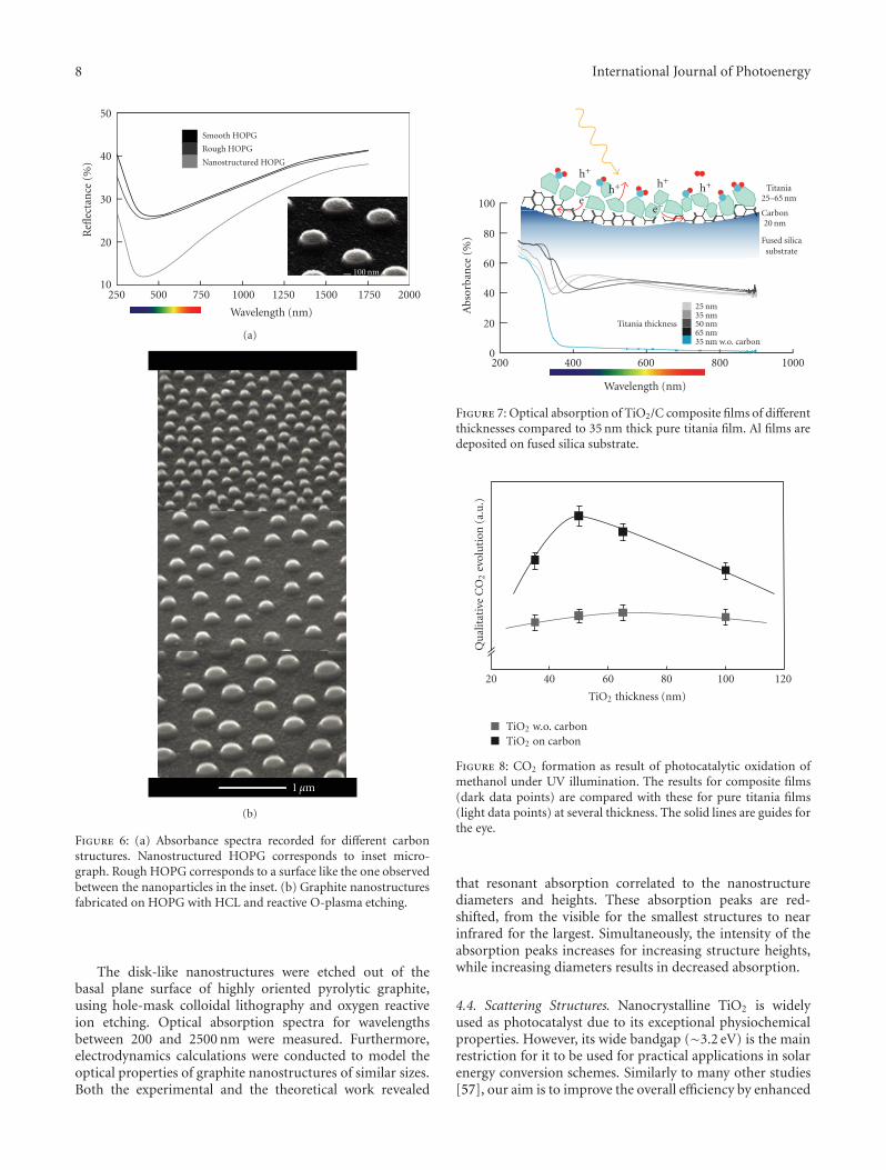
bond formation (0.5–6.5 eV). This should allow one tocreate conditions and propose schemes for enhanced (solar)light absorption in nanostructured materials and utilize thedeposited energy to run chemical transformations such aswater splitting. Figure 4, presenting previously unpublishedresults, shows that the extinction spectra of these structuresare readily tuned via the metal particles’ size.
In the case of plasmon-enhanced photochemistry, anarea pioneered by Brus in the early eighties [41], bothradiative and nonradiative enhancement pathways have beenpursued, as illustrated in an extensive review article byWatanabe et al. [42]. To give two representative examples,the photocatalytic degradation of methylene blue was foundto be significantly increased on nanocomposite photocata-lysts consisting of silver nanoparticles embedded in titania.Radiative energy transfer from the Ag nanoparticles to thesemiconductor was claimed to be the origin of increasedefficiency [43, 44]. Tian and Tatsuma, on the other hand,reported that ethanol and methanol can be photocatalyticallyoxidized by gold nanoparticle—nanoporous TiO2 compos-ites (at the expense of oxygen reduction) under visible lightillumination [45]. In this case, photoexcitation of the goldnanoparticles was followed by simultaneous charge transfer
of electrons from the gold to the TiO2 conduction band andfrom a donor in solution to the gold nanoparticle.
The main idea behind our photodesorption study [8]was to investigate how the shape and size of silver clusterson a graphite surface will influence the interaction of lightwith adsorbate covered surface. Since the optical propertiesof the clusters are dominated by plasmon excitations, thephotoinduced transformations will be indicative for theirdecay mechanisms. This was done by monitoring the changesin cross section for photodesorption of NO. NO was chosenas the probe molecule since its photoactivity on silver is wellknown. The photodesorption of NO from a silver substrateoccurs via hot-electron scattering at the 2π∗ resonance ofadsorbed NO with the hot carriers created in the substrateupon photon absorption (substrate-mediated hot electrondriven process) [46, 47]. Therefore, an experiment allowingcomparison between the desorption cross sections in thecases of resonantly and nonresonantly excited nanoparticleswill be indicative for the role of the plasmon particles andtheir energy dissipation.
The composition of the experimental model system wasbased on the following reasons. Silver clusters are known fortheir strong plasmonic response in the blue and near UV
6 International Journal of Photoenergy
DR ∼ 60 nmDR ∼ 60 nm
2.521.510.50
Coverage (1016 at. cm−2)
Init
ialp
hot
oyie
ld(a
.u.)
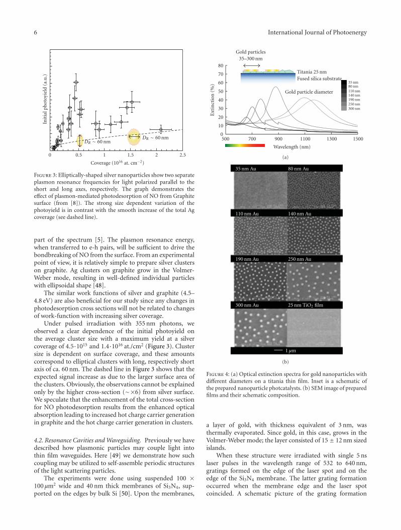
Figure 3: Elliptically-shaped silver nanoparticles show two separateplasmon resonance frequencies for light polarized parallel to theshort and long axes, respectively. The graph demonstrates theeffect of plasmon-mediated photodesorption of NO from Graphitesurface (from [8]). The strong size dependent variation of thephotoyield is in contrast with the smooth increase of the total Agcoverage (see dashed line).
part of the spectrum [5]. The plasmon resonance energy,when transferred to e-h pairs, will be sufficient to drive thebondbreaking of NO from the surface. From an experimentalpoint of view, it is relatively simple to prepare silver clusterson graphite. Ag clusters on graphite grow in the Volmer-Weber mode, resulting in well-defined individual particleswith ellipsoidal shape [48].
The similar work functions of silver and graphite (4.5–4.8 eV) are also beneficial for our study since any changes inphotodesorption cross sections will not be related to changesof work-function with increasing silver coverage.
Under pulsed irradiation with 355 nm photons, weobserved a clear dependence of the initial photoyield onthe average cluster size with a maximum yield at a silvercoverage of 4.5·1015 and 1.4·1016 at./cm2 (Figure 3). Clustersize is dependent on surface coverage, and these amountscorrespond to elliptical clusters with long, respectively shortaxis of ca. 60 nm. The dashed line in Figure 3 shows that theexpected signal increase as due to the larger surface area ofthe clusters. Obviously, the observations cannot be explainedonly by the higher cross-section (∼×6) from silver surface.We speculate that the enhancement of the total cross-sectionfor NO photodesorption results from the enhanced opticalabsorption leading to increased hot charge carrier generationin graphite and the hot charge carrier generation in clusters.
4.2. Resonance Cavities and Waveguiding. Previously we havedescribed how plasmonic particles may couple light intothin film waveguides. Here [49] we demonstrate how suchcoupling may be utilized to self-assemble periodic structuresof the light scattering particles.
The experiments were done using suspended 100 ×100 μm2 wide and 40 nm thick membranes of Si3N4, sup-ported on the edges by bulk Si [50]. Upon the membranes,
Gold particles35–300 nm
Titania 25 nmFused silica substrate
Gold particle diameter
35 nm80 nm110 nm140 nm190 nm250 nm300 nm
150013001100900700500
Wavelength (nm)
0
10
20
30
40
50
60
70
80
Ext
inct
ion
(%)
(a)
35 nm Au 80 nm Au
110 nm Au 140 nm Au
190 nm Au 250 nm Au
300 nm Au 25 nm TiO2 film
1 μm
(b)
Figure 4: (a) Optical extinction spectra for gold nanoparticles withdifferent diameters on a titania thin film. Inset is a schematic ofthe prepared nanoparticle photcatalysts. (b) SEM image of preparedfilms and their schematic composition.
a layer of gold, with thickness equivalent of 3 nm, wasthermally evaporated. Since gold, in this case, grows in theVolmer-Weber mode; the layer consisted of 15 ± 12 nm sizedislands.
When these structure were irradiated with single 5 nslaser pulses in the wavelength range of 532 to 640 nm,gratings formed on the edge of the laser spot and on theedge of the Si3N4 membrane. The latter grating formationoccurred when the membrane edge and the laser spotcoincided. A schematic picture of the grating formation

International Journal of Photoenergy 7
Incominglight
Waveguided light
500 nm
1 μm
1 μm
(a)
(b)
(c)
(d)
Figure 5: (a) Plasmonic particles scatter incoming coherent light into the underlying waveguide analogously with Figure 1(b). Due tostimulated emission of radiation from the particles into the waveguide, the guided light is coherent. Superposition of the incident light andthe waveguided results in an amplitude modulated standing wave. Its time averaged intensity is here depicted as a sine curve. The plasmonicparticles anneal (coalesce) at the time averaged intensity maxima of this modulated wave (blue particles) hereby forming the gratings. (b)Fringes formed at the intersection of the laser spot edge and the membrane edge. (c) Fringes formed on the laser spot edge. (d) Fringesformed on the membrane edge.
mechanism is presented in Figure 5(a) together with SEMmicrographs of resulting gratings, from Figures 5(b) to 5(d).
The key mechanism behind the grating formation is theamplitude modulation of the field intensity on the metalsurface arising when the waveguided field and the incidentfield superimpose. The time averaged energy density may beexpressed according to
E20 + E2
wg
2+ E0Ewg cos
[(k0x − kwg
)x + ϕ0 − ϕwg
]. (5)
Here E0 and Ewg denote the amplitudes of the incident andwaveguided electric fields, respectively, k0x and kwg denotetheir wavevectors projected on the propagation direction ofthe guided wave, and finally, ϕ0 and ϕwg their phases. Theperiodicity of the fringes is hereby given by
2π∣∣∣k0x − kwg
∣∣∣ . (6)
This self-assembly of periodic gratings on a waveguide mightbecome a useful tool in the fabrication of plasmonic lighttrapping devises in combination with particle shape controlmethods [51].
4.3. Geometrical Optical Resonance. Carbon materials areknown for their very specific optical properties. For example,the relative high refractive index and moderate dispersion
explain the brilliance of diamonds; the electron structureof amorphous carbon and graphite explains their strongabsorption in the visible range [52]. The discovery of newcarbon allotropes, the fullerenes, carbon nanotubes, andmore recently graphene (single layers of graphite) [53–55]was noticed by directing most of the optical studies ofnanosize carbon structures toward them. However, fabri-cation and exploration of the properties of nanostructuresof the conventional carbon materials, glassy carbon (GC),and highly oriented pyrolytic graphite (HOPG) is of greatinterest per se and for comparison. Recently, we performeda systematic investigation of the correlation between opticalabsorption and the size of graphite nanostructures [56].Samples with structure diameters ranging from 160 to330 nm and heights from 60 to 190 nm were prepared.
In order to better understand the role and properties ofcarbon (graphite) substrate, we developed a process for fab-rication of carbon nanostructures on the surfaces of highlyoriented pyrolytic graphite (HOPG) and glassy carbon (GC)samples, using hole-mask colloidal lithography and oxygenreactive ion etching (RIE). Identical preparation schemesapplied to the two materials yield structures with remarkablydifferent shape and sizes. For example, 361 nm high and37 nm diameter structures on glassy carbon compared to120 nm high and 119 nm diameter structures on HOPG, seeFigure 6(b). An important property of these structures, in thecontext of photo catalytic applications, is their strong opticalabsorption in the visible range.
8 International Journal of Photoenergy
100 nm
Smooth HOPG
Rough HOPG
Nanostructured HOPG
20001750150012501000750500250
Wavelength (nm)
10
20
30
40
50
Refl
ecta
nce
(%)
(a)
1 μm
(b)
Figure 6: (a) Absorbance spectra recorded for different carbonstructures. Nanostructured HOPG corresponds to inset micro-graph. Rough HOPG corresponds to a surface like the one observedbetween the nanoparticles in the inset. (b) Graphite nanostructuresfabricated on HOPG with HCL and reactive O-plasma etching.
The disk-like nanostructures were etched out of thebasal plane surface of highly oriented pyrolytic graphite,using hole-mask colloidal lithography and oxygen reactiveion etching. Optical absorption spectra for wavelengthsbetween 200 and 2500 nm were measured. Furthermore,electrodynamics calculations were conducted to model theoptical properties of graphite nanostructures of similar sizes.Both the experimental and the theoretical work revealed
25 nm35 nm50 nm65 nm35 nm w.o. carbon
Titania thickness
Titania25–65 nm
Carbon20 nm
Fused silicasubstrate
h+h+h+
h+
e−e−
1000800600400200
Wavelength (nm)
0
20
40
60
80
100
Abs
orba
nce
(%)
Figure 7: Optical absorption of TiO2/C composite films of differentthicknesses compared to 35 nm thick pure titania film. Al films aredeposited on fused silica substrate.
TiO2 w.o. carbonTiO2 on carbon
12010080604020
TiO2 thickness (nm)
Qu
alit
ativ
eC
O2
evol
uti
on(a
.u.)
Figure 8: CO2 formation as result of photocatalytic oxidation ofmethanol under UV illumination. The results for composite films(dark data points) are compared with these for pure titania films(light data points) at several thickness. The solid lines are guides forthe eye.
that resonant absorption correlated to the nanostructurediameters and heights. These absorption peaks are red-shifted, from the visible for the smallest structures to nearinfrared for the largest. Simultaneously, the intensity of theabsorption peaks increases for increasing structure heights,while increasing diameters results in decreased absorption.
4.4. Scattering Structures. Nanocrystalline TiO2 is widelyused as photocatalyst due to its exceptional physiochemicalproperties. However, its wide bandgap (∼3.2 eV) is the mainrestriction for it to be used for practical applications in solarenergy conversion schemes. Similarly to many other studies[57], our aim is to improve the overall efficiency by enhanced

International Journal of Photoenergy 9
solar light absorption in the visible regime. We work withTiO2 deposited on graphitic-like carbon film [58] as shownin Figure 7. Additionally to the enhanced absorption in thevisible, the carbon film is expected to promote efficientseparation of photogenerated charge carriers because of itsanisotropic conductivity for electrons and holes [59, 60] Asthe photoreaction occurs on the surface of the TiO2 catalyst,it is of great interest to investigate thickness dependence ofcharge transport in the titania films and how the presence ofcarbon film affects the size of crystallites.
Both carbon and titania films were prepared by e-beam evaporation and DC reactive magnetron sputtering,respectively, at room temperature on a fused silica substrate.Postdeposition annealing was carried out to reduce internalstresses and improve crystallinity in the film at 800◦C and500◦C for carbon and TiO2, respectively. Optical measure-ments of the composite films with different thicknessesare illustrated in Figure 7. The general observation is thatcomposite films absorb more in the visible than pure titaniafilms. Most importantly, the absorption threshold of TiO2
has red shifted for composite films.The catalytic activity of the films was tested in the
reaction of photo-oxidation of methanol to CO2 and water.The measurements were made in a, for this purposeconstructed, minireactor (∼880 μL volume) in batch modeunder UV light illumination of 120 mW/cm2. The productswere monitored in situ by a mass spectrometer coupled tothe reactor via a capillary. The rates of CO2 formation asa function of photocatalysts composition were obtained bymonitoring m/z = 44 mass spectrometer signal and are sum-marized in Figure 8. According to Figure 8, composite filmsclearly have enhanced photoactivity compared to pure titaniafilms. The observed enhancement of photocatalytic activityis assigned to synergy effects at the carbon/TiO2 interface,resulting in smaller titania crystallites and anisotropic chargecarrier transport, which in turn reduces their recombinationprobability.
Variation in photoactivity with the thickness of thetitania layer, both for pure and composite films, can beseen from the figure. The activity gradually increases upto certain thickness after which it starts to decrease. Oncethe film thickness reaches optimum value (∼mean free pathdistance), it encounters more scattering on its way to thesurface. As a consequence, the photoactivity decreases atthicknesses beyond the optimum due to enhanced trappingof charge carriers although the optical absorption volumeof the films increases. Overall, this measurement clearlydiscriminates the effect of thickness on charge transport andphotoactivity as discussed above.
5. Conclusions
With this paper, we have brushed the surface of whatis possible to achieve in light harvesting with the aid ofnanoscience and nanotechnology. Owing to miniaturizedlight trapping structures and enhanced absorption crosssections, solar devices may be designed with thicknesses wellbelow the charge carrier diffusion lengths with maintained,or even altered, light harvesting efficiency.
Acknowledgments
Support by Swedish Foundation for Strategic Research(SSF, RAM08-0109) and Northen European InnovativeEnergy Research Programme (N-INNER, project #30938-Solar Hydrogen) is gratefully acknowledged.
References
[1] R. C. Willson and A. V. Mordvinov, “Secular total solar irra-diance trend during solar cycles 21-23,” Geophysical ResearchLetters, vol. 30, no. 5, 2003.
[2] M. B. McElroy, The Atmospheric Environment : Effects ofHuman Activity, Princeton University Press, Princeton, NJ,USA, 2002.
[3] J. T. Yates Jr., “Photochemistry on TiO2: mechanisms behindthe surface chemistry,” Surface Science, vol. 603, no. 10–12, pp.1605–1612, 2009.
[4] M. Born and E. Wolf, Principles of Optics : ElectromagneticTheory of Propagation, Interference and Diffraction of Light,Cambridge University Press, New York, NY, USA, 7th edition,1999.
[5] U. Kreibig and M. Vollmer, Optical Properties of Metal Clusters,Springer Series in Materials Science, Springer, New York, NY,USA, 1995.
[6] C. J. Wu and D. B. Wittry, “Investigation of minority-carrier diffusion lengths by electron bombardment of Schottkybarriers,” Journal of Applied Physics, vol. 49, no. 5, pp. 2827–2836, 1978.
[7] H. J. Hovel, Solar Cells. Semiconductors an Semimetals, Aca-demic Press, New York, NY, USA, 1975.
[8] K. Wettergren, B. Kasemo, and D. Chakarov, “Photodesorp-tion of NO from graphite(0 0 0 1) surface mediated by silverclusters,” Surface Science, vol. 593, no. 1–3, pp. 235–241, 2005.
[9] P. Campbell and M. A. Green, “Light trapping properties ofpyramidally textured surfaces,” Journal of Applied Physics, vol.62, no. 1, pp. 243–249, 1987.
[10] P. Campbell and M. A. Green, “High performance lighttrapping textures for monocrystalline silicon solar cells,” SolarEnergy Materials and Solar Cells, vol. 65, no. 1–4, pp. 369–375,2001.
[11] C. Heine and R. H. Morf, “Submicrometer gratings for solar-energy applications,” Applied Optics, vol. 34, no. 14, pp. 2476–2482, 1995.
[12] S. Ito, T. N. Murakami, P. Comte et al., “Fabrication of thinfilm dye sensitized solar cells with solar to electric powerconversion efficiency over 10%,” Thin Solid Films, vol. 516, no.14, pp. 4613–4619, 2008.
[13] L. I. Halaoui, N. M. Abrams, and T. E. Mallouk, “Increasingthe conversion efficiency of dye-sensitized TiO photoelectro-chemical cells by coupling to photonic crystals,” The Journal ofPhysical Chemistry B, vol. 109, no. 13, pp. 6334–6342, 2005.
[14] P. Bermel, C. Luo, L. Zeng, L. C. Kimerling, and J. D.Joannopoulos, “Improving thin-film crystalline silicon solarcell efficiencies with photonic crystals,” Optics Express, vol. 15,no. 25, pp. 16986–17000, 2007.
[15] K. J. Vahala, “Optical microcavities,” Nature, vol. 424, no.6950, pp. 839–846, 2003.
[16] J. B. Pendry, “Negative refraction makes a perfect lens,”Physical Review Letters, vol. 85, no. 18, pp. 3966–3969, 2000.
[17] C. M. Soukoulis, M. Kafesaki, and E. N. Economou,“Negative-index materials: new frontiers in optics,” AdvancedMaterials, vol. 18, no. 15, pp. 1941–1952, 2006.
10 International Journal of Photoenergy
[18] A. P. Alivisatos, “Semiconductor clusters, nanocrystals, andquantum dots,” Science, vol. 271, no. 5251, pp. 933–937, 1996.
[19] R. D. Schaller and V. I. Klimov, “High efficiency carriermultiplication in PbSe nanocrystals: implications for solarenergy conversion,” Physical Review Letters, vol. 92, no. 18,Article ID 186601, 4 pages, 2004.
[20] R. D. Schaller, M. Sykora, J. M. Pietryga, and V. I. Klimov,“Seven excitons at a cost of one: redefining the limits forconversion efficiency of photons into charge carriers,” NanoLetters, vol. 6, no. 3, pp. 424–429, 2006.
[21] A. Shabaev, AL. L. Efros, and A. J. Nozik, “Multiexcitongeneration by a single photon in nanocrystals,” Nano Letters,vol. 6, no. 12, pp. 2856–2863, 2006.
[22] I. Paci, J. C. Johnson, X. Chen et al., “Singlet fission fordye-sensitized solar cells: can a suitable sensitizer be found?”Journal of the American Chemical Society, vol. 128, no. 51, pp.16546–16553, 2006.
[23] H. A. Atwater and A. Polman, “Plasmonics for improvedphotovoltaic devices,” Nature Materials, vol. 9, no. 3, pp. 205–213, 2010.
[24] H. R. Stuart and D. G. Hall, “Enhanced dipole-dipole inter-action between elementary radiators near a surface,” PhysicalReview Letters, vol. 80, no. 25, pp. 5663–5666, 1998.
[25] H. R. Stuart and D. G. Hall, “Island size effects in nanoparticle-enhanced photodetectors,” Applied Physics Letters, vol. 73, no.26, pp. 3815–3817, 1998.
[26] F. U. J. Tsai, J. Y. Wang, J. J. Huang, Y. W. Kiang, and C.C. Yang, “Absorption enhancement of an amorphous Si solarcell through surface plasmon-induced scattering with metalnanoparticles,” Optics Express, vol. 18, no. 13, pp. A207–A220,2010.
[27] D. S. Wiersma, R. Sapienza, S. Mujumdar, M. Colocci, M.Ghulinyan, and D. L. Pavesi, “Optics of nanostructureddielectrics,” Journal of Optics A: Pure and Applied Optics, vol.7, no. 2, pp. S190–S197, 2005.
[28] B. Mayer and S. Madronich, “Actinic flux and photolysis inwater droplets: mie calculations and geometrical optics limit,”Atmospheric Chemistry and Physics, vol. 4, no. 8, pp. 2241–2250, 2004.
[29] V. E. Ferry, L. A. Sweatlock, D. Pacifici, and H. A. Atwater,“Plasmonic nanostructure design for efficient light couplinginto solar cells,” Nano Letters, vol. 8, no. 12, pp. 4391–4397,2008.
[30] W. Bai, Q. Gan, F. Bartoli et al., “Design of plasmonic backstructures for efficiency enhancement of thin-film amorphousSi solar cells,” Optics Letters, vol. 34, no. 23, pp. 3725–3727,2009.
[31] M. Kirkengen, J. Bergli, and Y. M. Galperin, “Direct generationof charge carriers in c-Si solar cells due to embeddednanoparticles,” Journal of Applied Physics, vol. 102, no. 9,Article ID 093713, 2007.
[32] K. Kempa, J. Rybczynski, Z. Huang et al., “Carbon nanotubesas optical antennae,” Advanced Materials, vol. 19, no. 3, pp.421–426, 2007.
[33] P. V. Kamat, “Harvesting photons with carbon nanotubes,”Nano Today, vol. 1, no. 4, pp. 20–27, 2006.
[34] G. Calzaferri, M. Pauchard, H. Maas, S. Huber, A. Khatyr, andT. Schaafsma, “Photonic antenna system for light harvesting,transport and trapping,” Journal of Materials Chemistry, vol.12, no. 1, pp. 1–13, 2002.
[35] V. P. Zhdanov and B. Kasemo, “Nanometer-sized antenna forenhancement of absorption of light by dye molecules,” AppliedPhysics Letters, vol. 84, no. 10, pp. 1748–1749, 2004.
[36] D. M. Schaadt, B. Feng, and E. T. Yu, “Enhanced semiconduc-tor optical absorption via surface plasmon excitation in metalnanoparticles,” Applied Physics Letters, vol. 86, no. 6, Article ID063106, pp. 1–3, 2005.
[37] M. Westphalen, U. Kreibig, J. Rostalski, H. Luth, and D.Meissner, “Metal cluster enhanced organic solar cells,” SolarEnergy Materials and Solar Cells, vol. 61, no. 1, pp. 97–105,2000.
[38] R. Corkish, M. A. Green, and T. Puzzer, “Solar energycollection by antennas,” Solar Energy, vol. 73, no. 6, pp. 395–401, 2002.
[39] C. Langhammer, B. Kasemo, and I. Zoric, “Absorption andscattering of light by Pt, Pd, Ag, and Au nanodisks: absolutecross sections and branching ratios,” The Journal of ChemicalPhysics, vol. 126, no. 19, Article ID 194702, 11 pages, 2007.
[40] J. W. Schwede, I. Bargatin, D. C. Riley et al., “Photon-enhancedthermionic emission for solar concentrator systems,” NatureMaterials, vol. 9, no. 9, pp. 762–767, 2010.
[41] L. Brus, “Noble metal nanocrystals: plasmon electron transferphotochemistry and single-molecule raman spectroscopy,”Accounts of Chemical Research, vol. 41, no. 12, pp. 1742–1749,2008.
[42] K. Watanabe, D. Menzel, N. Nilius, and H. J. Freund,“Photochemistry on metal nanoparticles,” Chemical Reviews,vol. 106, no. 10, pp. 4301–4320, 2006.
[43] K. Awazu, M. Fujimaki, C. Rockstuhl et al., “A plasmonicphotocatalyst consisting of silver nanoparticles embedded intitanium dioxide,” Journal of the American Chemical Society,vol. 130, no. 5, pp. 1676–1680, 2008.
[44] P. Christopher, D. B. Ingram, and S. Linic, “Enhancingphotochemical activity of semiconductor nanoparticles withoptically active Ag nanostructures: photochemistry mediatedby Ag surface plasmons,” The Journal of Physical Chemistry C,vol. 114, no. 19, pp. 9173–9177, 2010.
[45] Y. Tian and T. Tatsuma, “Mechanisms and applications ofplasmon-induced charge separation at TiO2 films loaded withgold nanoparticles,” Journal of the American Chemical Society,vol. 127, no. 20, pp. 7632–7637, 2005.
[46] S. K. So, R. Franchy, and W. Ho, “Photodesorption of NO fromAg(111) and Cu(111),” The Journal of Chemical Physics, vol.95, no. 2, pp. 1385–1399, 1991.
[47] R. T. Kidd, D. Lennon, and S. R. Meech, “Comparative studyof the primary photochemical mechanisms of nitric oxideand carbonyl sulfide on Ag(111),” The Journal of PhysicalChemistry B, vol. 103, no. 35, pp. 7480–7488, 1999.
[48] H. Hovel, B. Grimm, M. Pollmann, and B. Reihl, “Cluster-substrate interaction on a femtosecond time scale revealed by ahigh-resolution photoemission study of the fermi-level onset,”Physical Review Letters, vol. 81, no. 21, pp. 4608–4611, 1998.
[49] L. Eurenius, C. Hagglund, E. Olsson, B. Kasemo, andD. Chakarov, “Grating formation by metal-nanoparticle-mediated coupling of light into waveguided modes,” NaturePhotonics, vol. 2, no. 6, pp. 360–364, 2008.
[50] A. W. Grant, Q. H. Hu, and B. Kasemo, “Transmissionelectron microscopy ’windows’ for nanofabricated structures,”Nanotechnology, vol. 15, no. 9, pp. 1175–1181, 2004.
[51] R. Jin, Y. C. Cao, E. Hao, G. S. Metraux, G. C. Schatz, andC. A. Mirkin, “Controlling anisotropic nanoparticle growththrough plasmon excitation,” Nature, vol. 425, no. 6957, pp.487–490, 2003.
[52] N. Laidani, R. Bartali, G. Gottardi, M. Anderle, and P.Cheyssac, “Optical absorption parameters of amorphous car-bon films from Forouhi-Bloomer and Tauc-Lorentz models: a
International Journal of Photoenergy 11
comparative study,” Journal of Physics Condensed Matter, vol.20, no. 1, Article ID 015216, 2008.
[53] A. K. Geim and K. S. Novoselov, “The rise of graphene,”Nature Materials, vol. 6, no. 3, pp. 183–191, 2007.
[54] S. Iijima, “Helical microtubules of graphitic carbon,” Nature,vol. 354, no. 6348, pp. 56–58, 1991.
[55] H. W. Kroto, J. R. Heath, S. C. O’Brien, R. F. Curl, and R.E. Smalley, “C60: buckminsterfullerene,” Nature, vol. 318, no.6042, pp. 162–163, 1985.
[56] H. Fredriksson, T. Pakizeh, M. Kall, B. Kasemo, and D.Chakarov, “Resonant optical absorption in graphite nanos-tructures,” Journal of Optics A: Pure and Applied Optics, vol.11, no. 11, Article ID 114022, 2009.
[57] A. L. Linsebigler, G. Lu, and J. T. Yates, “Photocatalysis onTiO2 surfaces: principles, mechanisms, and selected results,”Chemical Reviews, vol. 95, no. 3, pp. 735–758, 1995.
[58] R. Sellappan and D. Chakarov, “Nanostructured TiO2/Carbonfilms with enhanced photocatalytic activity for water dissoci-ation,” Journal of Molecular Catalysis A, vol. 335, no. 1-2, pp.136–144, 2011.
[59] P. R. Wallace, “The band theory of graphite,” Physical Review,vol. 71, no. 9, pp. 622–634, 1947.
[60] Y. Yao, G. Li, S. Ciston, R. M. Lueptow, and K. A. Gray,“Photoreactive TiO2/carbon nanotube composites: synthesisand reactivity,” Environmental Science and Technology, vol. 42,no. 13, pp. 4952–4957, 2008.
Hindawi Publishing CorporationInternational Journal of PhotoenergyVolume 2011, Article ID 798051, 12 pagesdoi:10.1155/2011/798051
Review Article
Photocatalytic Enhancement forSolar Disinfection of Water: A Review
J. Anthony Byrne,1 Pilar A. Fernandez-Ibanez,2 Patrick S. M. Dunlop,1
Dheaya M. A. Alrousan,1 and Jeremy W. J. Hamilton1
1 Nanotechnology and Integrated BioEngineering Centre, University of Ulster, Newtownabbey BT37 0QB, Northern Ireland, UK2 Plataforma Solar de Almerıa (CIEMAT), Crta Senes km 4, 04200 Tabernas, Spain
Correspondence should be addressed to J. Anthony Byrne, [email protected]
Received 31 August 2010; Accepted 24 December 2010
Academic Editor: Mohamed Sabry Abdel-Mottaleb
Copyright © 2011 J. Anthony Byrne et al. This is an open access article distributed under the Creative Commons AttributionLicense, which permits unrestricted use, distribution, and reproduction in any medium, provided the original work is properlycited.
It is estimated that 884 million people lack access to improved water supplies. Many more are forced to rely on supplies that aremicrobiologically unsafe, resulting in a higher risk of waterborne diseases, including typhoid, hepatitis, polio, and cholera. Dueto poor sanitation and lack of clean drinking water, there are around 4 billion cases of diarrhea each year resulting in 2.2 milliondeaths, most of these are children under five. While conventional interventions to improve water supplies are effective, there isincreasing interest in household-based interventions to produce safe drinking water at an affordable cost for developing regions.Solar disinfection (SODIS) is a simple and low cost technique used to disinfect drinking water, where water is placed in transparentcontainers and exposed to sunlight for 6 hours. There are a number of parameters which affect the efficacy of SODIS, includingthe solar irradiance, the quality of the water, and the nature of the contamination. One approach to SODIS enhancement is theuse of semiconductor photocatalysis to produce highly reactive species that can destroy organic pollutants and inactivate waterpathogens. This paper presents a critical review concerning semiconductor photocatalysis as a potential enhancement technologyfor solar disinfection of water.
1. Introduction
Water is the most important natural resource in the worldand availability of safe drinking water is a high priorityissue for human existence and quality of life. Unfortunately,water resources are coming under increasing pressure due topopulation growth, over-use and wastage. The World HealthOrganization (WHO) estimates that 884 million people lackaccess to improved water supplies. Many more are forced torely on sources that are microbiologically unsafe, resulting ina higher risk of waterborne disease transmission, includingtyphoid, hepatitis and cholera [1–3].
As ever, the poor are the worst affected and, in developingcountries, 50% of the population are exposed to pollutedwater sources which, along with inadequate supplies of waterfor personal hygiene and poor sanitation, are the main
contributors to an estimated 4 billion cases of diarrhea eachyear. These factors result in an estimated 2.2 million deathseach year, the majority of which are children under the age offive [1].
The provision of piped-in water supplies is an importantlong-term goal; however, the WHO and the United NationsChildren’s Fund (UNICEF) acknowledge that we are unlikelyto meet the Millennium Development Goal (MDG) targetof halving the proportion of the people without sustainableaccess to safe drinking water and basic sanitation by 2015.While conventional interventions to improve water suppliesat source (point of distribution) have long been recognizedas effective in preventing diarrhoea, more recent reviewshave shown household-based (point-of-use) interventions tobe significantly more effective than those at the source. Asa result, there is increasing interest in such household-based
2 International Journal of Photoenergy
interventions that deliver the health benefits associated withconsumption of safe drinking water via low cost technologies[4].
In 2008, Clasen and Haller reported on the cost and costeffectiveness of house-hold based interventions to preventdiarrhoea [4]. They compared the following: chlorinationusing sodium hypochlorite following the “Safe Water Sys-tem” (SWS) developed and promoted by the US Centersfor Disease Control and Prevention (CDC), gravity filtrationusing either commercial “candle” style gravity filters orlocally fabricated pot-style filters developed by Potters forPeace, solar disinfection following the “SODIS” method inwhich clear 2 L PET bottles are filled with raw water and thenexposed to the sun for 6–48 h, and flocculation disinfectionusing Procter & Gambles PUR sachets, which combine aniron-based flocculant with a chlorine-based disinfectant andtreat water in 10 L batches. They concluded that household-based chlorination was the most cost-effective. Solar disin-fection (SODIS) was only slightly less cost-effective, owingto its almost identical cost but marginally lower overall effec-tiveness. Given that household-based chlorination requiresthe distribution of sodium hypochlorite, solar disinfectionhas a major advantage in terms of nonreliance on chemicaldistribution. Sunlight is widely and freely available on Earthand the combined effects of IR, visible and UV energyfrom the sun can inactivate pathogenic organisms presentin water. There are a number of parameters which affect theefficacy of the SODIS process, including the solar irradiance,the quality of the water to be treated, and the nature ofthe contamination—as some pathogens are more resistantto SODIS than others. Furthermore, SODIS enhancementtechnologies may improve the process effectiveness withoutsubstantially increasing the cost. One such approach is theuse of semiconductor photocatalysis.
Semiconductor photocatalysis uses light along witha semiconductor material to produce highly oxidative speciesthat destroy organic pollutants in water and inactivatepathogenic microorganisms [5–10]. The process occurs atatmospheric pressure and ambient temperature, without therequirement for consumable chemicals (except for oxygenfrom the air). Photocatalysis may be able to provide a lowcost and simple solution to the purification of water indeveloping regions where solar irradiation can be employed.
This paper presents a critical review concerning semicon-ductor photocatalysis as a potential enhancement technologyfor the solar disinfection of water. The purpose of this reviewis to inform the nonexpert with respect to solar disinfection,and photocatalytic disinfection. For more detailed informa-tion the reader is referred to the scientific papers cited.
2. Solar Disinfection of Water (SODIS)
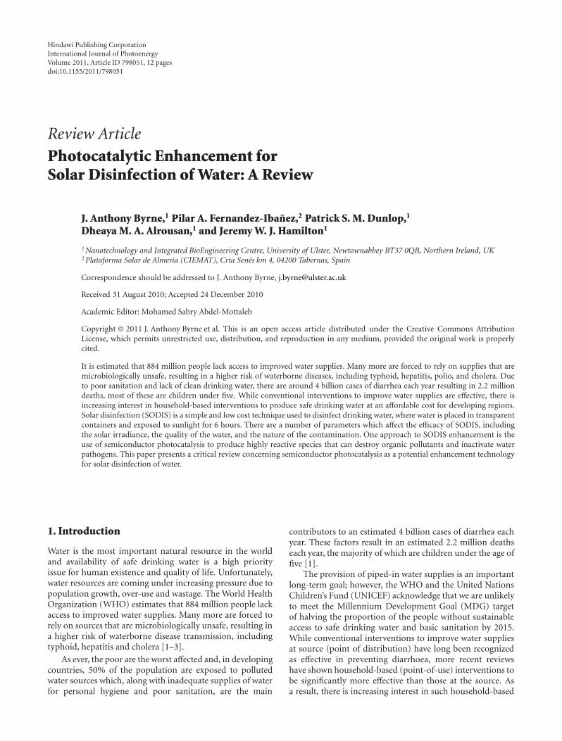
SODIS is a simple and low cost technique used to disinfectcontaminated drinking water. Transparent bottles (prefer-ably PET) are filled with contaminated water and placed indirect sunlight for a minimum of 6 hours. Following expo-sure, the water is safe to drink as the viable pathogen loadcan be significantly decreased. Simple guidance for the useof SODIS is given in Figure 1. SODIS is used by an estimated
4.5 million regular users worldwide, predominately in Africa,Latin America, and Asia, and is recognised and promoted bythe WHO [11, 12].
SODIS harnesses light and thermal energy to inactivatepathogens via a synergistic mechanism [13]. Around 4–6%of the solar spectrum reaching the surface of the Earth is inthe UV domain, with maximum reported value of around50 W/m2 [14]. UV radiation (200–400 nm) can be classifiedas UVA (320–400 nm), UVB (280–320 nm), and UVC (200–280 nm). UVC is absorbed by the ozone layer along with aproportion of the UVB; therefore UVA represents the mainfragment of solar ultraviolet radiation reaching the earth’ssurface.
Disinfection of water using solar energy has been carriedout since Egyptian times. The process was first studied andreported in scientific literature by London-based scientistsDownes and Blunt in the late 1870s [15] and was effectivelyrediscovered as a low-cost water disinfection method by Acraet al. in the late 1970s [16, 17]. The main findings of this workwere that Escherichia coli was more resistant to SODIS thanother organisms tested, and as such E. coli should be usedas an indicator organism for SODIS efficiency, akin to thepresence of viable faecal coliforms as an indicator of efficacyfor conventional disinfection processes. Furthermore, it isthe UV component of sunlight, and to a lesser extent theblue end of the visible spectrum, that is mainly responsiblefor the biocidal action observed during SODIS. Wegelinet al. from the Swiss Federal Institute of Aquatic Scienceand Technology (Eawag) reported on SODIS in terms ofthe scope of the process and the dose of radiation required[18]. They concurred with the conclusions of Acra et al.and reported that to obtain a 3-log reduction in the viablenumbers of E. coli a cumulative exposure dose of 2000 kJ/m2
(350–450 nm) was required. The same dose was found toinactivate bacteriophage f2 whereas picornavirus requiredtwice this dose. Water temperatures above 50◦C significantlyincreased the rate of bacterial inactivation. The researchteam at Eawag have significantly contributed to the scientificdevelopment, standardisation, and promotion of the SODISprocess through the development of the online informationnetwork and the publication and distribution of the SODISManual and associated education resources [12].
Laboratory studies have demonstrated the effects of keyoperational parameters such as light intensity and wave-length, solar exposure time, availability of oxygen, turbid-ity, and temperature [19, 20]. The SODIS mechanism isunderstood to involve a number of biocidal pathways basedupon absorption of UVA radiation and thermal inactivation.Direct UVA exposure can induce cellular membrane damageand delay microbial growth [21]. The biocidal action of UVAhas also been attributed to the production of reactive oxygenspecies (ROS) which are generated from dissolved oxygenin water [22] and the photosensitisation of molecules inthe cell, and/or any naturally occurring dissolved organicmatter that can absorb photons of wavelengths between320–400 nm, to induce photochemical reactions [23]. Thethermal effect has been attributed to the high absorption ofred and infrared photons by water. At temperatures below40◦C, the thermal effect is negligible with UVA inactivation
International Journal of Photoenergy 3
(1) Wash the bottle well thefirst time you use
Fill the bottle3/4 full with
water
Shake the bottle for20 seconds (4)
Now fill up the bottlefully and close the lid
(6)
Place the bottles ona black iron sheet
The water is nowready for
consumption
Expose the bottle to thesun from morning untilevening for at least six
hours
Or put them onthe roof
Figure 1: SODIS process—www.sodis.ch.
mechanisms dominating the inactivation process. Significantbactericidal action is evident at temperatures above 40–45◦Cwith a synergistic SODIS process observed at temperaturesabove 45◦C [13, 19, 23–25]. Detailed genetic assessment hasalso been used to probe the biocidal mechanism of SODIS[26, 27].
Researchers have shown SODIS to be effective againsta wide range of microorganisms responsible for diarrhealillness [28–30]. The inactivation of resistant protozoa hasalso been reported [31–33]. Field trials have demonstrateda significant health benefits from consumption of SODIStreated water [34, 35]. The effectiveness of SODIS againstcholera was also demonstrated in a Kenyan health impactassessment, where an 86% reduction cholera cases wasobserved in households regularly using SODIS [36].
Studies to improve the efficiency of the SODIS processusing low-cost, commonly available materials have been con-ducted [37–40]; however, the simple approach of exposinga 2 L PET bottle to full sun for a minimum of 6 hours is themost commonly promoted and practiced method.
3. Enhancement Technologies for SODIS
There are several drawbacks of “conventional” SODIS tech-nology. The use of PET bottles allows for only small volumesto be treated (2-3 L), and the process efficiency is dependenton a range of environmental parameters including the solarirradiance (which depends on the latitude, time of day,and atmospheric conditions), the initial water quality forexample organic loading, turbidity, level, and nature of thebacterial contamination. The resistance that microorganismsdisplay to solar disinfection leads to variation in treatmenttimes. Malato et al. reviewed the reported inactivation timerequired for a range of microorganisms using SODIS underca. 1 kW/m2 global irradiance [10]. These vary enormouslyfrom 20 min for Campylobacter jejuni to 8 h for Cryp-tosporidium parvum oocysts. For Bacillus subtilis endospores,
no inactivation was observed after 8 hours of SODIStreatment. SODIS is user dependent in that it requires theuser to ‘time’ the exposure and as such there is no qualityassurance in the process and as such, lack of compliance withthe recommended protocol is a major issue.
There are a number of ways to improve or enhance theconventional SODIS process, including the design of SODISbags where the solar dose per volume is increased, the useof UVA dosimetric sensors which indicate to the user whenthe desired dose has been received by the water, the designof customised SODIS treatment systems which maximise thesolar dose using compound parabolic collectors (CPC) andmay include UVA feedback sensors for automated control,and the use of semiconductor photocatalysis to enhance thetreatment efficacy.
3.1. SODIS Bags. The SODIS method can be enhanced byuse of a personal SODIS-reactor which would maximisethe area for photon collection and minimise the pathlength for light penetration through the water to be treated.Furthermore, these SODIS bags could be deployed inemergency situations where access to drinking water is animmediate issue for example flooding or earthquake. Thelatter application can be limited due to the lack of PETbottles in disaster areas whereas bags have the advantagethat they can easily be transported and stored in largequantities. Eawag has launched a project to develop specificSODIS bags, and several bag models are being developedin collaboration with partners from the private sector. Aprototype is currently being field tested together with localorganisations in Bolivia, DR Congo, Kenya, Nepal, andNicaragua [41].
3.2. UV Dosimetric Indicators. Professor Mills’ group atthe University of Strathclyde has been investigating theuse of photocatalytic systems as intelligent inks [42, 43].As titanium dioxide (TiO2) is excited by UVA light, these

4 International Journal of Photoenergy
0
0.1
Abo
srba
nce
at66
0n
m
0.2
0.3
0.4
0.5
0.6
0.7
0.8
0.9
0 5 10 15 20
Time (min)
Figure 2: Colourimetric UVA dosimetric indicators—UVA expo-sure photo-reduced MB (blue) the LMB (white) (UVA dose =9.0 kJ/m2), MB subsequently reformed via oxidation in the dark.
systems may be used as UVA dosimetric indicators. At theUniversity of Ulster, we have tested a simple prototype systemto measure UVA dose utilising the photocatalytic reductionof methylene blue (MB) to leuco-Methylene Blue (LMB)(method adopted from Mills, Lee, and Sheridan [43]).
In the presence of the hole scavenger (glycerol), methy-lene blue is photocatalytically reduced to colorless leuco-methylene blue, and the rate of decolouration is dependenton the UVA intensity (Figure 2). In the dark and in thepresence of oxygen, the reduced form is reoxidised backto methylene blue. This results in a simple reversible UVAdosimetric indicator which could be utilised to provide somequality assurance for the SODIS user. There are a wide rangeof dyes or inks that could be utilised in these systems toprovide simple dosimetric indicators for corresponding toUVA doses required for SODIS.
3.3. Compound Parabolic Collectors. Fernandez-Ibanez andMalato at the Plataforma Solar de Almeria (PSA) in Spainhave focused on the use of nonconcentrating solar collectorsfor the enhancement of solar disinfection. CompoundParabolic Collectors (CPC’s) are nonimaging systems whichcollect diffuse radiation. The collected energy is homoge-neously distributed across the absorber surface. CPCs do notrely solely on direct solar radiation and are therefore effectiveeven on cloudy days. In addition, they collect radiationindependently of the direction of sunlight and do not requiresun tracking.
The SODIS process relies heavily on the solar UVAwhich, as received at sea level, is composed of roughlysimilar portions of both direct and diffuse electromagneticradiation. Given the diffuse nature of the UVA and thecylindrical shape of SODIS bottles, the use of sunlightcollecting systems based on nonimaging optics has obviouspotential. Navntoft et al. demonstrated the use of CPCtechnology to enhance the efficacy of SODIS on sunny andcloudy days [25]. The major advantage of CPC technologyis that the concentration factor remains constant for all
Length = 1.5 m
Diameter = 0.05 m
Sampling valve Closed end
(a)
Glass tube
(b)
SamplingFlow meter
Thermocouple
F
CPC Tube
PumpT
Tank
(c)
Figure 3: (a) Glass tube configuration. (b) Tube with CPC collectorconfiguration. (c) Flow diagram of the solar CPC reactor (withpermission from [48]).
values of sun zenith angle within the acceptance anglelimit; therefore, it is theoretically possible to design largervolume SODIS systems. For example, recent work showedthe effective inactivation of E. coli K12 in well water usinga 25 L SODIS reactor with CPC [44]. Studies using CPC solarreactors including titanium dioxide as a photocatalyst haveshown increased disinfection in comparison to SODIS alone[45–47].
Ubomba-Jaswa et al. investigated the effect of UVAdose on the inactivation efficiency of 3 types of SODISreactors: borosilicate glass tubes (static batch), borosilicateglass tubes with compound parabolic collector (recirculatingbatch), and borosilicate glass tubes with CPC (recirculatingbatch) (Figures 3 and 4) [48]. They used E. coli K12 as themodel microorganism suspended in natural well water anddemonstrated inactivation of approximately 6-log colonyforming units (CFU) mL−1 following receipt of a totaluninterrupted minimum dose of >108 kJ/m2 (295–385 nm).
4. Semiconductor Photocatalysis
4.1. Mechanism of Photocatalysis. When a semiconductor isirradiated with light of wavelength equal or greater than itsband gap, energy is absorbed resulting in the promotion ofelectrons from the valence band to the conduction band,and the formation of electron-hole pairs (e− and h+) [5].These charge carriers can recombine, with the energy beingreemitted as light or heat, or they may migrate to the catalystsurface where they can participate in redox reactions at the

International Journal of Photoenergy 5
Figure 4: Borosilicate glass tubes with CPC.
For TiO2
hν ≥ 3.2 eV
O2
O•− ,2 H2O2
•OH
OH
h+
e−
Figure 5: Schematic representation of the mechanism of photo-catalysis on titanium dioxide particles.
particle-solution interface [8] (Figure 5). The reactive oxygenspecies (ROS) produced, including the hydroxyl radical, arevery active, indiscriminate oxidants [49] destroying a largevariety of chemical contaminants in water and also causingfatal damage to microorganisms [50]. The final productsof the photocatalytic degradation of pollutants (given longenough treatment time) are CO2, H2O, and respectiveinorganic acids or salts.
For more detailed information on the mechanisms ofsemiconductor photocatalysis, the reader is referred to oneof the many excellent reviews [5–10].
4.2. Photocatalytic Materials. Several compounds have beeninvestigated as potential semiconductor photocatalysts,including metal oxides (TiO2, ZnO, ZrO2, V2O5, Fe2O3,SnO2) and metal sulphides (CdS, ZnS) [51, 52]. Amongstthese, the most popular photocatalyst for use in water treat-ment applications is titanium dioxide. TiO2 is a wide bandsemiconductor (band gap = 3.2 eV for anatase); therefore, itrequires UV excitation. To improve efficiency in solar appli-cations, visible light active materials are desirable. However,while absorbing a greater number of solar photons, thesmaller band gap gives a narrower voltage window to drivethe redox reactions at the particle-solution interface. Metalsulphide semiconductors, which absorb in the visible regionof the spectrum, tend to undergo photo-anodic corrosion[53]. Considering cost, chemical and photochemical stability,
availability, and lack of toxicity, the most suitable catalystreported to date for the treatment of water is TiO2 [54].
4.3. Immobilised versus Suspended Photocatalyst. The photo-catalyst can be utilised in aqueous suspension or it may beimmobilised on a supporting solid substrate. Most studieshave reported that suspension reactors are more efficientdue to large surface area available for redox reactions [55],however; the main drawback of using nano or micro-particles in suspension is the requirement for posttreatmentseparation and recycling of the catalyst, potentially makingthe treatment more complex and expensive. Therefore,treatment reactors utilising immobilised TiO2 have gainedattention. There are a wide range of methodologies availablefor the preparation of immobilised photocatalyst films ona range of supporting substrates, and a careful reactor designis required to prevent efficiency loss due to a reduction incatalyst surface area and poor mass transfer of reactants tothe photocatalyst surface [56].
4.4. Photocatalytic Disinfection of Water. Matsunaga et al.reported the first application of TiO2 photocatalysis forthe inactivation of bacteria in 1985 [57]. Since then, therehave been a large number of research publications dealingwith the inactivation of microorganisms including bacteria,viruses, protozoa, fungi, and algae. Blake et al. carried outan extensive review of the microorganisms reported to beinactivated by photocatalysis [51]. In 2007, McCullagh et al.reviewed the application of photocatalysis for the disinfec-tion of water contaminated with pathogenic microorganisms[58]. In 2009, Malato et al. published an extensive reviewon the decontamination and disinfection of water by solarphotocatalysis [10] and, in 2010, Dalrymple et al. reviewedthe proposed mechanisms and kinetic models widely used inphotocatalytic disinfection studies [59].
In most photocatalytic disinfection studies, the hydroxylradical is suggested to be the primary species responsiblefor microorganism inactivation; however, some papers doreport involvement of other ROS, such as H2O2, O•−
2
[60–63]. These reactive species can cause fatal damage tomicroorganisms by disruption of the cell membrane or byattacking DNA and RNA [51]. Other modes of action TiO2
photocatalysis have been proposed, including damage to therespiratory system within the cells [64] and loss of fluidityand increased ion permeability in the cell membrane [62].Detailed spectroscopy-based studies attributed cell death tolipid peroxidation of bacterial cell membrane [61–63]. Theperoxidation of the unsaturated phospholipids contained inthe bacterial cell membrane results in loss of respiratoryactivity [65] and/or leads to a loss of fluidity and increasedion permeability [62]. It has also been suggested that cellmembrane damage can open the way for further oxidativeattack of internal cellular components, ultimately resultingin cell death [65].
Research at the University of Ulster has been mainlyconcerned with the use of immobilised TiO2 films preparedby the deposition of Evnoik (Degussa) P25 onto a rangeof supporting substrates, including borosilicate glass, ITOglass, and titanium metal. For example, Alrousan et al.

6 International Journal of Photoenergy
0 25 50 75 100 125 150 175 200 225
Time (min)
0
10
20
30
40
50
60
70
80
90
Surv
ival
(%)
100
Figure 6: Comparison between photocatalytic and photolyticinactivation of E. coli in surface and distilled water (TiO2, UV,Distilled water) , (TiO2, UV, Surface water) •, (UV, Distilledwater) , (UV, Surface water) , Dark control (with permission,from [66]).
reported on the photocatalytic inactivation of E. coli insurface water using immobilised nanoparticle TiO2 films[66]. In this work, P25 was immobilized onto borosilicateglass using a dip coating method. The photoreactor wasa custom-built stirred tank reactor which had excellentmixing and good mass transfer properties. The catalyst wasirradiated in a back-face configuration that is, the lightpassed through the glass to excite the photocatalyst onthe surface. It was found that the rate of photocatalyticinactivation of E. coli was more efficient with UVA-TiO2
than direct photolytic inactivation with UVA alone, forE. coli suspended in both distilled water and surface water(Figure 6). The optimum catalyst loading for the inactivationwas determined to be 0.5 mg/cm2, approximately half thatreported for photocatalytic degradation of formic acid andatrazine in the same reactor, under the same incident lightintensity.
The organic and inorganic content of the surface waterled to a reduction in the rate of photocatalytic disinfection incomparison to that observed in distilled water. The effect ofselected individual constituents present in the surface waterwas examined to identify the main constituent responsiblefor the reduction in the rate of photocatalytic disinfection.The presence of inorganic ions, that is, sulphate and nitratereduced the rate of photocatalytic inactivation, with sulphatehaving a more pronounced effect than nitrate. The presenceof organic matter was found to be the dominating parameterresponsible for the decrease in the rate of photocatalyticdisinfection. The presence of inorganic ions will lead toa reduction in efficiency either by absorption of light,competing for ROS, or by adsorption to the catalyst surface.Organic matter will compete for ROS and may compete forphoton absorption. The efficacy of photocatalytic disinfec-tion will therefore be strongly dependent on the initial waterquality. Where the water to be treated is of poor quality, a pre-treatment stage, for example, simple filtration or settling,may be desirable prior to photocatalytic treatment.
Bacterial cells have been described as a rather easytarget for disinfectants, with bacterial spores and protozoa
suggested as more robust target organisms. Clostridium per-fringens spores have been reported to be chlorine resistant atlevels used in potable water supplies. Dunlop et al. reportedon the photocatalytic inactivation of Clostridium perfringensspores on TiO2 electrodes [67]. The TiO2 electrodes weremade using electrophoretic immobilisation of commerciallyavailable TiO2 powders onto conducting supports, that is,indium-doped tin oxide-coated glass, titanium metal, andtitanium alloy. The photocatalytic inactivation of E. coliand C. perfringens spores in water was observed on allimmobilised TiO2 films under UVA irradiation. The rateof photocatalytic inactivation of E. coli was found to beone order of magnitude greater than that of C. perfringensspores, demonstrating the greater resistance of the spores toenvironmental stress. In this work, it was shown that theapplication of an external electrical bias (electrochemicallyassisted photocatalysis) significantly increased the rate ofphotocatalytic disinfection of C. perfringens spores. Theeffect of incident light intensity and initial spore loadingwere investigated, and disinfection kinetics were determinedto be pseudo-first order. This work demonstrated that UVAphotocatalysis is effective against bacterial spores whichare more resistant to environmental stress, including UVAirradiation, than bacterial cells.
Cryptosporidium species are waterborne, protozoanparasites that infect a wide range of vertebrates. The lifecycle involves the production of an encysted stage (oocyst)which is discharged in the faeces of their host. The disease,Cryptosporidiosis, in humans usually results in self-limitedwatery diarrhoea but has far more devastating effects onimmunocompromised patients (e.g., AIDS patients) and canbe life-threatening as a result of dehydration caused bychronic diarrhoea. Owing to their tough outer walls, theoocysts are highly resistant to disinfection and can survive forseveral months in standing water. Cryptosporidium oocyststherefore present as an excellent challenge for disinfectiontechnologies. Sunnotel et al. reported on the photocatalyticinactivation of Cryptosporidium parvum oocysts on nanos-tructured titanium dioxide films (Figure 7) [68].
The photocatalytic inactivation of the oocysts was shownto occur in Ringer’s buffer solution (78.4% after 180 min)and surface water (73.7% after 180 min). Scanning electronmicroscopy (SEM) confirmed cleavage at the suture lineof oocyst cell walls, revealing large numbers of empty(ghost) cells after exposure to photocatalytic treatment. Nosignificant inactivation was observed in the oocysts exposedto UVA radiation alone demonstrating the substantial benefitin the addition of TiO2 as a photocatalyst.
It is clear from the literature, that in lab scale reactors,photocatalysis under UVA irradiation is more efficient thanUVA irradiation alone for the disinfection of water con-taminated with pathogenic microorganisms. Therefore, it isessential that photocatalytic reactors are tested for disinfec-tion under real sun conditions either on small scale batch(personal use) or at pilot scale (aimed at household or smallcommunity use), and using real water sources.
Gelover et al. studied small-scale batch disinfection inplastic bottles containing spring water naturally pollutedwith coliform bacteria, with and without the addition of

International Journal of Photoenergy 7
0 30 60 90 120 150 1800
20
40
60
80
100
Dark control
UV only
Surface water
Ringers
C.p
arvu
moo
cyst
viab
ility
(%)
Figure 7: Photocatalytic inactivation of C. parvum oocysts sus-pended in Ringer’s solution and surface water (with permissionfrom [68]).
60◦19◦
Figure 8: Simple solar collector made from 5 wooden sheetscovered with aluminium foil (with permission from [69]).
TiO2 [69]. The bottles were mounted in simple home-made solar collectors (Figure 8). Two litre PET bottles werefilled with spring water and exposed to direct sunlight.The microbial loading was typically 2.5× 10³ MPN/100 mL(most probable number) of total coliforms and 9.0× 10²
MPN/100 mL of faecal coliforms.TiO2 was coated onto small Pyrex-glass cylinders, using
a sol-gel method, and these were placed inside each bottle.It was found that photocatalytically enhanced SODIS was byfar more effective than SODIS alone for the inactivation ofboth the total coliforms and the faecal coliforms (Figure 9).They measured bacterial regrowth following treatment andfound that regrowth was observed with SODIS alone, butnot with photocatalytically enhanced SODIS. This is animportant finding, as bacteria have repair mechanisms whichallow recovery following stress/injury and demonstrates thedifferences in the kill mechanisms involved in SODIS andphotocatalytic disinfection.
With respect to larger-scale systems, Fernandez-Ibanezet al. reported on the pilot-scale photocatalytic disinfectionof water under real sun conditions using a photoreactorwith CPC [70]. The experiments were carried out under
0 20 40
Irradiation time (min)
60 800
300
600
900
1200
0.1
1
43% remaining
SODIS
SODIS
SODIS + TiO2
SODIS with TiO2
Irradiance
0% remaining Irra
dian
ce(W
/m2)
MP
N/1
00m
L
10
100
1000
10000
Figure 9: Decrease in faecal coliforms in natural spring waterexposed to direct sunlight, comparing SODIS to TiO2-enhancedSODIS (with permission from [69]).
sunlight at the Plataforma Solar de Almeria in southernSpain using compound parabolic collectors. The pilot plantconsisted of three CPC collectors, each containing twoPyrex tubes (50 mm inner diameter, 1.5 m long), witha collector surface area of 0.25 m2 and a total reactorvolume treated of 11 L. Experiments were performed withsuspended TiO2 and, following modification to the reactor,with supported/immobilised TiO2. In both cases, Degussa,P25 was employed as the photocatalyst. In the immobilisedstudy, the catalyst was fixed onto glass fibre using SiO2 asan inorganic binder. E. coli was used as the model microor-ganism suspended in distilled water. The photocatalyticsuspension reactor was the most efficient, followed by theimmobilised photocatalytic reactor, with SODIS being theleast efficient treatment (Figure 10).
Further work undertaken by the group at PlataformaSolar de Almeria investigated the effect of UV intensityand dose on SODIS and photocatalytically enhanced SODIS[71]. The aim of the work was to study the dependenceon solar irradiation conditions under natural sunlightusing three microorganisms, E. coli K-12 culture and twowild strains Fusarium solani and Fusarium anthophilum.Photocatalytic disinfection experiments were carried outwith TiO2 supported on a paper matrix held concentricallywithin the CPC glass tube reactors described above, andwith TiO2 in the form of a slurry in Pyrex glass bottlereactors. The experiments were performed with differentilluminated reactor surfaces, in different seasons of the year,and under changing weather conditions (i.e., cloudy andsunny days). Photocatalysis did not increase the rate ofdisinfection following receipt of the minimum solar dose;however, the solar-only disinfection was more susceptible tochanges in solar irradiation than photocatalytic disinfection,that is, where light intensities were generally low or therewas greater availability of diffuse UVA, the inclusion of thephotocatalyst provided a significant benefit.
5. Issues to Be Addressed
5.1. Photoreactor Design. The SODIS process dependsmainly on the UVA wavelengths present in sunlight. Solar
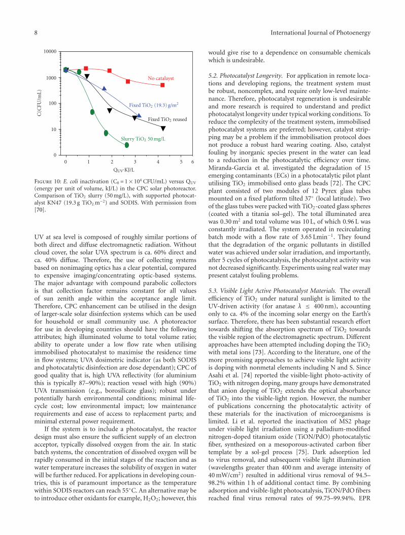
8 International Journal of Photoenergy
0 1 2 3 4 5 6
QUV’KJ/L
0
10
100
1000
10000
C(C
FU/m
L)
No catalayst
Fixed TiO2 reused
Fixed TiO2 (19.3) g/m2
Slurry TiO2 50 mg/L
Figure 10: E. coli inactivation (C0 = 1× 10⁴ CFU/mL) versus QUV
(energy per unit of volume, kJ/L) in the CPC solar photoreactor.Comparison of TiO2 slurry (50 mg/L), with supported photocat-alyst KN47 (19.3 g TiO2.m−2) and SODIS. With permission from[70].
UV at sea level is composed of roughly similar portions ofboth direct and diffuse electromagnetic radiation. Withoutcloud cover, the solar UVA spectrum is ca. 60% direct andca. 40% diffuse. Therefore, the use of collecting systemsbased on nonimaging optics has a clear potential, comparedto expensive imaging/concentrating optic-based systems.The major advantage with compound parabolic collectorsis that collection factor remains constant for all valuesof sun zenith angle within the acceptance angle limit.Therefore, CPC enhancement can be utilised in the designof larger-scale solar disinfection systems which can be usedfor household or small community use. A photoreactorfor use in developing countries should have the followingattributes; high illuminated volume to total volume ratio;ability to operate under a low flow rate when utilisingimmobilised photocatalyst to maximise the residence timein flow systems; UVA dosimetric indicator (as both SODISand photocatalytic disinfection are dose dependant); CPC ofgood quality that is, high UVA reflectivity (for aluminiumthis is typically 87–90%); reaction vessel with high (90%)UVA transmission (e.g., borosilicate glass); robust underpotentially harsh environmental conditions; minimal life-cycle cost; low environmental impact; low maintenancerequirements and ease of access to replacement parts; andminimal external power requirement.
If the system is to include a photocatalyst, the reactordesign must also ensure the sufficient supply of an electronacceptor, typically dissolved oxygen from the air. In staticbatch systems, the concentration of dissolved oxygen will berapidly consumed in the initial stages of the reaction and aswater temperature increases the solubility of oxygen in waterwill be further reduced. For applications in developing coun-tries, this is of paramount importance as the temperaturewithin SODIS reactors can reach 55◦C. An alternative may beto introduce other oxidants for example, H2O2; however, this
would give rise to a dependence on consumable chemicalswhich is undesirable.
5.2. Photocatalyst Longevity. For application in remote loca-tions and developing regions, the treatment system mustbe robust, noncomplex, and require only low-level mainte-nance. Therefore, photocatalyst regeneration is undesirableand more research is required to understand and predictphotocatalyst longevity under typical working conditions. Toreduce the complexity of the treatment system, immobilisedphotocatalyst systems are preferred; however, catalyst strip-ping may be a problem if the immobilisation protocol doesnot produce a robust hard wearing coating. Also, catalystfouling by inorganic species present in the water can leadto a reduction in the photocatalytic efficiency over time.Miranda-Garcıa et al. investigated the degradation of 15emerging contaminants (ECs) in a photocatalytic pilot plantutilising TiO2 immobilised onto glass beads [72]. The CPCplant consisted of two modules of 12 Pyrex glass tubesmounted on a fixed platform tilted 37◦ (local latitude). Twoof the glass tubes were packed with TiO2-coated glass spheres(coated with a titania sol–gel). The total illuminated areawas 0.30 m2 and total volume was 10 L, of which 0.96 L wasconstantly irradiated. The system operated in recirculatingbatch mode with a flow rate of 3.65 Lmin−1. They foundthat the degradation of the organic pollutants in distilledwater was achieved under solar irradiation, and importantly,after 5 cycles of photocatalysis, the photocatalyst activity wasnot decreased significantly. Experiments using real water maypresent catalyst fouling problems.
5.3. Visible Light Active Photocatalyst Materials. The overallefficiency of TiO2 under natural sunlight is limited to theUV-driven activity (for anatase λ ≤ 400 nm), accountingonly to ca. 4% of the incoming solar energy on the Earth’ssurface. Therefore, there has been substantial research efforttowards shifting the absorption spectrum of TiO2 towardsthe visible region of the electromagnetic spectrum. Differentapproaches have been attempted including doping the TiO2
with metal ions [73]. According to the literature, one of themore promising approaches to achieve visible light activityis doping with nonmetal elements including N and S. SinceAsahi et al. [74] reported the visible-light photo-activity ofTiO2 with nitrogen doping, many groups have demonstratedthat anion doping of TiO2 extends the optical absorbanceof TiO2 into the visible-light region. However, the numberof publications concerning the photocatalytic activity ofthese materials for the inactivation of microorganisms islimited. Li et al. reported the inactivation of MS2 phageunder visible light irradiation using a palladium-modifiednitrogen-doped titanium oxide (TiON/PdO) photocatalyticfiber, synthesized on a mesoporous-activated carbon fibertemplate by a sol-gel process [75]. Dark adsorption ledto virus removal, and subsequent visible light illumination(wavelengths greater than 400 nm and average intensity of40 mW/cm2) resulted in additional virus removal of 94.5–98.2% within 1 h of additional contact time. By combiningadsorption and visible-light photocatalysis, TiON/PdO fibersreached final virus removal rates of 99.75–99.94%. EPR

International Journal of Photoenergy 9
measurements confirmed the production of •OH radicals byTiON/PdO under visible light illumination. Wu et al. alsoreported visible-light-induced photocatalytic inactivation ofbacteria by composite photocatalysts of palladium oxideand nitrogen-doped TiO2 [76]. The PdO/TiON catalystswere tested for visible-light-activated photocatalysis usinggram-negative organisms that is, E. coli and Pseudomonasaeruginosa and the gram-positive organism Staphylococcusaureus. Their disinfection data showed that the PdO/TiONphotocatalysts had a much better visible photocatalytic activ-ity than either palladium-doped (PdO/TiO2) or nitrogen-doped titanium oxide (TiON). The light source used in thiswork was a metal halogen desk lamp with a low UV output(<0.01 mW/cm2 for λ ≤ 400 nm). While these photocatalystsshow promise, there was no comparison with undoped TiO2
and solar-simulated light (which has around 5% UV) was notused.
In many cases, the UV activity of undoped TiO2 is muchgreater than the visible light activity of the doped material.Therefore, for solar applications, the photocatalysts shouldbe tested under simulated solar irradiation or under real sunconditions. Indeed, Rengifo-Herrera and Pulgarin recentlyreported on the photocatalytic activity of N, S codopedand N-doped commercial anatase (Tayca TKP 102) TiO2
powders towards phenol oxidation and E. coli inactivationunder simulated solar light irradiation [77]. However, thesenovel materials did not present an enhancement for thephotocatalytic degradation of phenol or the photocatalyticinactivation of E. coli under simulated solar light, as com-pared to Degussa P25. They suggest that while the N, orN-S co-doped TiO2, may show a visible light response, thelocalized states responsible for the visible light absorption donot play an important role in the photocatalytic activity.
More research is required to determine if visible lightactive materials can deliver an increase in the efficiency ofphotocatalysis under solar irradiation.
6. Conclusions
SODIS is a simple and low cost technique used to disinfectcontaminated drinking water. Transparent bottles (prefer-ably PET) are filled with contaminated water and placedin direct sunlight for a minimum of 6 hours. Followingexposure, the water is safe to drink as the viable pathogenload can be significantly decreased. The process has approx-imately 4.5 million regular users, predominately in Africa,Latin America, and Asia and is recognised and promotedby the WHO. However, there are several drawbacks with“conventional” SODIS technology. The use of PET bottlesallows for only small volumes to be treated (2-3 L) and theprocess efficiency is dependent on a range of environmentalparameters including the solar irradiance (which depends onthe latitude, time of day, and atmospheric conditions), theinitial water quality for example, organic loading, turbidity,and level and nature of the bacterial contamination. Thereare a number of ways to improve or enhance the conventionalSODIS process and these include the design of SODISbags where the solar dose per volume is increased, theuse of UV dosimetric indicators which measure the UV
dose and indicate to the user when the desired dose hasbeen received by the water, design of customised SODIStreatment systems which maximise the solar dose and theinclusion of UV feedback sensors for automated control,and the use of semiconductor photocatalysis to enhancethe treatment efficacy. Semiconductor photocatalysis hasbeen shown to be effective for the inactivation of a widerange of microorganisms at lab scale and under real sunconditions for both small-scale and large-scale applications.The use of CPC reactors enhances the efficiency of solar dis-infection and photocatalytically enhanced solar disinfection.Nevertheless, there are a number of issues to be addressedbefore photocatalytically enhanced solar disinfection can beeffectively deployed in developing regions. These includeimprovements in photoreactor design and the assessmentof photocatalyst longevity under real operating conditions.Future developments in relation to visible light activephotocatalytic materials may lead to more efficient solarphotocatalysis for the disinfection of water.
Acknowledgments
The authors wish to thank the European Commission forfinancial support in relation to the SODISWATER project(INCO-CT-2006-031650), the Spanish Ministry of Sci-ence and Innovation under the Consolider-Ingenio 2010programme (Project CSD2006-00044 TRAGUA), and theDepartment of Employment and Learning (Northern Ire-land) for funding DMA Alrousan, and the Department ofEmployment and Learning (Northern Ireland) for fundingDMA Alrousan, and DEL and Invest Northern Ireland forfunding under the US-Ireland Initiative for “DegradationMechanism of Cyanotoxins Using Novel Visible Light-Activated Titania (TiO2) Photocatlysts”.
References
[1] T. Clasen and P. Edmondson, “Sodium dichloroisocyanurate(NaDCC) tablets as an alternative to sodium hypochloritefor the routine treatment of drinking water at the householdlevel,” International Journal of Hygiene and EnvironmentalHealth, vol. 209, no. 2, pp. 173–181, 2006.
[2] WHO, “Economic and health effects of increasing coverageof low cost household drinking-water supply and sanitationinterventions to countries off-track to meet MDG target 10,”2007.
[3] J. D. Burch and K. E. Thomas, “Water disinfection for develop-ing countries and potential for solar thermal pasteurization,”Solar Energy, vol. 64, no. 1–3, pp. 87–97, 1998.
[4] T. F. Clasen and L. Haller, Water Quality Interventions toPrevent Diarrhoea: Cost and Cost-Effectiveness, WHO, 2008.
[5] A. Mills and S. Le Hunte, “An overview of semiconductorphotocatalysis,” Journal of Photochemistry and Photobiology A,vol. 108, no. 1, pp. 1–35, 1997.
[6] D. A. Tryk, A. Fujishima, and K. Honda, “Recent topics inphotoelectrochemistry: achievements and future prospects,”Electrochimica Acta, vol. 45, no. 15-16, pp. 2363–2376, 2000.
[7] D. Bahnemann, “Photocatalytic water treatment: solar energyapplications,” Solar Energy, vol. 77, no. 5, pp. 445–459, 2004.
[8] V. Augugliaro, M. Litter, L. Palmisano, and J. Soria, “Thecombination of heterogeneous photocatalysis with chemical
10 International Journal of Photoenergy
and physical operations: a tool for improving the photoprocessperformance,” Journal of Photochemistry and Photobiology C,vol. 7, no. 4, pp. 127–144, 2006.
[9] A. Fujishima, X. Zhang, and D. A. Tryk, “TiO2 photocatalysisand related surface phenomena,” Surface Science Reports, vol.63, no. 12, pp. 515–582, 2008.
[10] S. Malato, P. Fernandez-Ibanez, M. I. Maldonado, J. Blanco,and W. Gernjak, “Decontamination and disinfection of waterby solar photocatalysis: recent overview and trends,” CatalysisToday, vol. 147, no. 1, pp. 1–59, 2009.
[11] “SODIS Newsletter 2010 No. 1,” Swiss Federal Institute ofAquatic Science and Technology, 2010.
[12] SODIS, August 2010, http://www.sodis.ch/index.[13] K. G. McGuigan, T. M. Joyce, R. M. Conroy, J. B. Gillespie,
and M. Elmore-Meegan, “Solar disinfection of drinking watercontained in transparent plastic bottles: characterizing thebacterial inactivation process,” Journal of Applied Microbiology,vol. 84, no. 6, pp. 1138–1148, 1998.
[14] Y. D. Goswami, F. Kreith, and J. F. Kreider, Principles of SolarEngineering, Taylor and Francis, Philadelphia, Pa, USA, 2ndedition, 2000.
[15] A. Downes and T. P. Blunt, “The influence of light upon thedevelopment of bacteria,” Nature, vol. 16, pp. 402–218, 1877.
[16] A. Acra, Y. Karahagopian, Z. Raffoul, and R. Dajani, “Disin-fection of oral rehydration solutions by sunlight,” The Lancet,vol. 2, no. 8206, pp. 1257–1258, 1980.
[17] A. Acra, Z. Raffoul, and Y. Karahagopian, Solar Disinfectionof Drinking Water and Oral Rehydration Solutions, UNICEF,Paris, France, 1984.
[18] M. Wegelin, S. Canonica, K. Mechsner, T. Fleischmann,F. Pesaro, and A. Metzler, “Solar water disinfection: scope ofthe process and analysis of radiation experiments,” Journal ofWater Supply Research and Technology—Aqua, vol. 43, no. 4,pp. 154–169, 1994.
[19] M. Berney, H. U. Weilenmann, A. Simonetti, and T. Egli,“Efficacy of solar disinfection of Escherichia coli, Shigellaflexneri, Salmonella Typhimurium and Vibrio cholerae,”Journal of Applied Microbiology, vol. 101, no. 4, pp. 828–836,2006.
[20] R. H. Reed, “The inactivation of microbes by sunlight: solardisinfection as a water treatment process,” Advances in AppliedMicrobiology, vol. 54, pp. 333–365, 2004.
[21] A. Hamamoto, M. Mori, A. Takahashi et al., “New waterdisinfection system using UVA light-emitting diodes,” Journalof Applied Microbiology, vol. 103, no. 6, pp. 2291–2298, 2007.
[22] R. Khaengraeng and R. H. Reed, “Oxygen and photoinacti-vation of Escherichia coli in UVA and sunlight,” Journal ofApplied Microbiology, vol. 99, no. 1, pp. 39–50, 2005.
[23] P. M. Oates, P. Shanahan, and M. F. Polz, “Solar disinfection(SODIS): simulation of solar radiation for global assessmentand application for point-of-use water treatment in Haiti,”Water Research, vol. 37, no. 1, pp. 47–54, 2003.
[24] J. Blanco, S. Malato, P. Fernandez-Ibanez, D. Alarcon, W.Gernjak, and M. I. Maldonado, “Review of feasible solarenergy applications to water processes,” Renewable and Sus-tainable Energy Reviews, vol. 13, no. 6-7, pp. 1437–1445, 2009.
[25] C. Navntoft, E. Ubomba-Jaswa, K. G. McGuigan, and P.Fernandez-Ibanez, “Effectiveness of solar disinfection usingbatch reactors with non-imaging aluminium reflectors underreal conditions: natural well-water and solar light,” Journal ofPhotochemistry and Photobiology B, vol. 93, no. 3, pp. 155–161,2008.
[26] M. Berney, H. U. Weilenmann, and T. Egli, “Flow-cytometricstudy of vital cellular functions in Escherichia coli during solar
disinfection (SODIS),” Microbiology, vol. 152, no. 6, pp. 1719–1729, 2006.
[27] M. Berney, H. U. Weilenmann, and T. Egli, “Gene expressionof Escherichia coli in continuous culture during adaptation toartificial sunlight,” Environmental Microbiology, vol. 8, no. 9,pp. 1635–1647, 2006.
[28] S. C. Kehoe, M. R. Barer, L. O. Devlin, and K. G. McGuigan,“Batch process solar disinfection is an efficient means of disin-fecting drinking water contaminated with Shigella dysenteriaetype I,” Letters in Applied Microbiology, vol. 38, no. 5, pp. 410–414, 2004.
[29] J. Lonnen, S. Kilvington, S. C. Kehoe, F. Al-Touati, andK. G. McGuigan, “Solar and photocatalytic disinfection ofprotozoan, fungal and bacterial microbes in drinking water,”Water Research, vol. 39, no. 5, pp. 877–883, 2005.
[30] M. Boyle, C. Sichel, P. Fernandez-Ibanez et al., “Bactericidaleffect of solar water disinfection under real sunlight condi-tions,” Applied and Environmental Microbiology, vol. 74, no.10, pp. 2997–3001, 2008.
[31] K. G. McGuigan, F. Mendez-Hermida, J. A. Castro-Hermidaet al., “Batch solar disinfection inactivates oocysts of Cryp-tosporidium parvum and cysts of Giardia muris in drinkingwater,” Journal of Applied Microbiology, vol. 101, no. 2, pp.453–463, 2006.
[32] W. Heaselgrave, N. Patel, S. Kilvington, S. C. Kehoe, and K.G. McGuigan, “Solar disinfection of poliovirus and Acan-thamoeba polyphaga cysts in water—a laboratory study usingsimulated sunlight,” Letters in Applied Microbiology, vol. 43,no. 2, pp. 125–130, 2006.
[33] S. Mtapuri-Zinyowera, N. Midzi, C. E. Muchaneta-Kubara,T. Simbini, and T. Mduluza, “Impact of solar radiationin disinfecting drinking water contaminated with Giardiaduodenalis and Entamoeba histolytica/dispar at a point-of-usewater treatment,” Journal of Applied Microbiology, vol. 106, no.3, pp. 847–852, 2009.
[34] R. M. Conroy, M. Elmore-Meegan, T. Joyce, K. G. McGuigan,and J. Barnes, “Solar disinfection of drinking water anddiarrhoea in Maasai children: a controlled field trial,” TheLancet, vol. 348, no. 9043, pp. 1695–1697, 1996.
[35] R. M. Conroy, M. Elmore Meegan, T. Joyce, K. McGuigan,and J. Barnes, “Solar disinfection of water reduces diarrhoealdisease: an update,” Archives of Disease in Childhood, vol. 81,no. 4, pp. 337–338, 1999.
[36] R. M. Conroy, M. E. Meegan, T. Joyce, K. McGuigan, and J.Barnes, “Solar disinfection of drinking water protects againstcholera in children under 6 years of age,” Archives of Disease inChildhood, vol. 85, no. 4, pp. 293–295, 2001.
[37] B. Sommer, A. Marino, Y. Solarte et al., “SODIS—an emergingwater treatment process,” Journal of Water Supply Research andTechnology—Aqua, vol. 46, no. 3, pp. 127–137, 1997.
[38] S. C. Kehoe, T. M. Joyce, P. Ibrahim, J. B. Gillespie, R. A.Shahar, and K. G. McGuigan, “Effect of agitation, turbidity,aluminium foil reflectors and container volume on theinactivation efficiency of batch-process solar disinfectors,”Water Research, vol. 35, no. 4, pp. 1061–1065, 2001.
[39] M. B. Fisher, C. R. Keenan, K. L. Nelson, and B. M. Voelker,“Speeding up solar disinfection (SODIS): effects of hydrogenperoxide, temperature, pH, and copper plus ascorbate on thephotoinactivation of E. coli,” Journal of Water and Health, vol.6, no. 1, pp. 35–51, 2008.
[40] S. K. Mani, R. Kanjur, I. S. B. Singh, and R. H. Reed, “Com-parative effectiveness of solar disinfection using small-scalebatch reactors with reflective, absorptive and transmissive rearsurfaces,” Water Research, vol. 40, no. 4, pp. 721–727, 2006.

International Journal of Photoenergy 11
[41] M. Saladin, “SODIS bags for humanitarian aid,” March 2010,http://www.sodis.ch/index.
[42] S. K. Lee, M. Sheridan, and A. Mills, “Novel UV-activatedcolorımetric oxygen indicator,” Chemistry of Materials, vol. 17,no. 10, pp. 2744–2751, 2005.
[43] A. Mills, S. K. Lee, and M. Sheridan, “Development of a novelUV indicator and dosimeter film,” Analyst, vol. 130, no. 7, pp.1046–1051, 2005.
[44] E. Ubomba-Jaswa, P. Fernandez-Ibanez, C. Navntoft, M.Inmaculada Polo-Lopezb, and K. G. McGuigana, “Investigat-ing the microbial inactivation efficiency of a 25 L batch solardisinfection (SODIS) reactor enhanced with a compoundparabolic collector (CPC) for household use,” Journal ofChemical Technology and Biotechnology, vol. 85, no. 8, pp.1028–1037, 2010.
[45] A. Vidal, A. I. Dıaz, A. El Hraiki et al., “Solar photocatalysis fordetoxification and disinfection of contaminated water: pilotplant studies,” Catalysis Today, vol. 54, no. 2-3, pp. 283–290,1999.
[46] O. A. McLoughlin, P. Fernandez-Ibanez, W. Gernjak, S. MalatoRodriguez, and L. W. Gill, “Photocatalytic disinfection ofwater using low cost compound parabolic collectors,” SolarEnergy, vol. 77, no. 5, pp. 625–633, 2004.
[47] C. Navntoft, P. Araujo, M. I. Litter et al., “Field tests of thesolar water detoxification SOLWATER reactor in Los Pereyra,Tucuman, Argentina,” Journal of Solar Energy Engineering, vol.129, no. 1, pp. 127–134, 2007.
[48] E. Ubomba-Jaswa, C. Navntoft, M. I. Polo-Lopez, P.Fernandez-Ibanez, and K. G. McGuigan, “Solar disinfectionof drinking water (SODIS): an investigation of the effectof UV-A dose on inactivation efficiency,” Photochemical andPhotobiological Sciences, vol. 8, no. 5, pp. 587–595, 2009.
[49] C. Lee, Y. Lee, and J. Yoon, “Oxidative degradation ofdimethylsulfoxide by locally concentrated hydroxyl radicals instreamer corona discharge process,” Chemosphere, vol. 65, no.7, pp. 1163–1170, 2006.
[50] D. M. Blake, P. C. Maness, Z. Huang, E. J. Wolfrum, J. Huang,and W. A. Jacoby, “Application of the photocatalytic chemistryof titanium dioxide to disinfection and the killing of cancercells,” Separation and Purification Methods, vol. 28, no. 1, pp.1–50, 1999.
[51] J.-M. Herrmann, “Heterogeneous photocatalysis: fundamen-tals and applications to the removal of various types ofaqueous pollutants,” Catalysis Today, vol. 53, no. 1, pp. 115–129, 1999.
[52] C. Karunakaran, S. Senthilvelan, S. Karuthapandian, andK. Balaraman, “Photooxidation of iodide ion on somesemiconductor and non-semiconductor surfaces,” CatalysisCommunications, vol. 5, no. 6, pp. 283–290, 2004.
[53] K. G. Kanade, J. O. Baeg, U. P. Mulik, D. P. Amalnerkar, and B.B. Kale, “Nano-CdS by polymer-inorganic solid-state reaction:visible light pristine photocatalyst for hydrogen generation,”Materials Research Bulletin, vol. 41, no. 12, pp. 2219–2225,2006.
[54] M. I. Litter, “Heterogeneous photocatalysis: transition metalions in photocatalytic systems,” Applied Catalysis B, vol. 23,no. 2-3, pp. 89–114, 1999.
[55] J. A. Byrne, B. R. Eggins, N. M. D. Brown, B. McKinney, andM. Rouse, “Immobilisation of TiO2 powder for the treatmentof polluted water,” Applied Catalysis B, vol. 17, no. 1-2, pp. 25–36, 1998.
[56] T. A. McMurray, J. A. Byrne, P. S. M. Dunlop, J. G. M.Winkelman, B. R. Eggins, and E. T. McAdams, “Intrinsickinetics of photocatalytic oxidation of formic and oxalic acid
on immobilised TiO2 films,” Applied Catalysis A, vol. 262, no.1, pp. 105–110, 2004.
[57] T. Matsunaga, R. Tomoda, T. Nakajima, and H. Wake,“Photoelectrochemical sterilization of microbial cells by semi-conductor powders,” FEMS Microbiology Letters, vol. 29, no.1-2, pp. 211–214, 1985.
[58] C. Mccullagh, J. M. C. Robertson, D. W. Bahnemann, and P.K. J. Robertson, “The application of TiO2 photocatalysis fordisinfection of water contaminated with pathogenic micro-organisms: a review,” Research on Chemical Intermediates, vol.33, no. 3-5, pp. 359–375, 2007.
[59] O. K. Dalrymple, E. Stefanakos, M. A. Trotz, and D. Y.Goswami, “A review of the mechanisms and modeling ofphotocatalytic disinfection,” Applied Catalysis B, vol. 98, no.1-2, pp. 27–38, 2010.
[60] Z. Huang, P. C. Maness, D. M. Blake, E. J. Wolfrum,S. L. Smolinski, and W. A. Jacoby, “Bactericidal mode oftitanium dioxide photocatalysis,” Journal of Photochemistryand Photobiology A, vol. 130, no. 2-3, pp. 163–170, 2000.
[61] M. Wainwright, “Methylene blue derivatives—suitable pho-toantimicrobials for blood product disinfection?” Interna-tional Journal of Antimicrobial Agents, vol. 16, no. 4, pp. 381–394, 2000.
[62] K. Sunada, T. Watanabe, and K. Hashimoto, “Studies onphotokilling of bacteria on TiO2 thin film,” Journal of Photo-chemistry and Photobiology A, vol. 156, no. 1–3, pp. 227–233,2003.
[63] M. Cho, H. Chung, W. Choi, and J. Yoon, “Linear correlationbetween inactivation of E. coli and OH radical concentrationin TiO2 photocatalytic disinfection,” Water Research, vol. 38,no. 4, pp. 1069–1077, 2004.
[64] A. G. Rincon, C. Pulgarin, N. Adler, and P. Peringer, “Inter-action between E. coli inactivation and DBP-precursors—dihydroxybenzene isomers—in the photocatalytic process ofdrinking-water disinfection with TiO2 ,” Journal of Photochem-istry and Photobiology A, vol. 139, no. 2-3, pp. 233–241, 2001.
[65] A. G. Rincon and C. Pulgarin, “Field solar E. coli inactivationin the absence and presence of TiO2 : is UV solar dosean appropriate parameter for standardization of water solardisinfection?” Solar Energy, vol. 77, no. 5, pp. 635–648, 2004.
[66] D. M. A. Alrousan, P. S. M. Dunlop, T. A. McMurray, and J. A.Byrne, “Photocatalytic inactivation of E. coli in surface waterusing immobilised nanoparticle TiO2 films,” Water Research,vol. 43, no. 1, pp. 47–54, 2009.
[67] P. S. M. Dunlop, T. A. McMurray, J. W. J. Hamilton, and J. A.Byrne, “Photocatalytic inactivation of Clostridium perfringensspores on TiO2 electrodes,” Journal of Photochemistry andPhotobiology A, vol. 196, no. 1, pp. 113–119, 2008.
[68] O. Sunnotel, R. Verdoold, P. S. M. Dunlop et al., “Photocat-alytic inactivation of Cryptosporidium parvum on nanostruc-tured titanium dioxide films,” Journal of Water and Health, vol.8, no. 1, pp. 83–91, 2010.
[69] S. Gelover, L. A. Gomez, K. Reyes, and M. Teresa Leal, “Apractical demonstration of water disinfection using TiO2 filmsand sunlight,” Water Research, vol. 40, no. 17, pp. 3274–3280,2006.
[70] P. Fernandez, J. Blanco, C. Sichel, and S. Malato, “Waterdisinfection by solar photocatalysis using compound paraboliccollectors,” Catalysis Today, vol. 101, no. 3-4, pp. 345–352,2005.
[71] C. Sichel, J. Tello, M. de Cara, and P. Fernandez-Ibanez,“Effect of UV solar intensity and dose on the photocatalyticdisinfection of bacteria and fungi,” Catalysis Today, vol. 129,no. 1-2, pp. 152–160, 2007.

12 International Journal of Photoenergy
[72] N. Miranda-Garcıa, M. I. Maldonado, J. M. Coronado, andS. Malato, “Degradation study of 15 emerging contaminantsat low concentration by immobilized TiO2 in a pilot plant,”Catalysis Today, vol. 151, no. 1-2, pp. 107–113, 2010.
[73] J. W. J. Hamilton, J. A. Byrne, C. McCullagh, and P. S. M.Dunlop, “Electrochemical investigation of doped titaniumdioxide,” International Journal of Photoenergy, vol. 2008,Article ID 631597, 2008.
[74] R. Asahi, T. Morikawa, T. Ohwaki, K. Aoki, and Y. Taga,“Visible-light photocatalysis in nitrogen-doped titaniumoxides,” Science, vol. 293, no. 5528, pp. 269–271, 2001.
[75] Q. Li, M. A. Page, B. J. Marinas, and K. S. Jian, “Treatmentof coliphage MS2 with palladium-modified nitrogen-dopedtitanium oxide photocatalyst illuminated by visible light,”Environmental Science and Technology, vol. 42, no. 16, pp.6148–6153, 2008.
[76] P. Wu, R. Xie, J. A. Imlay, and J. K. Shang, “Visible-light-induced photocatalytic inactivation of bacteria by compositephotocatalysts of palladium oxide and nitrogen-doped tita-nium oxide,” Applied Catalysis B, vol. 88, no. 3-4, pp. 576–581,2009.
[77] J. A. Rengifo-Herrera and C. Pulgarin, “Photocatalytic activityof N, S co-doped and N-doped commercial anatase TiO2
powders towards phenol oxidation and E. coli inactivationunder simulated solar light irradiation,” Solar Energy, vol. 84,no. 1, pp. 37–43, 2010.

Hindawi Publishing CorporationInternational Journal of PhotoenergyVolume 2011, Article ID 139374, 6 pagesdoi:10.1155/2011/139374
Research Article
Studying the Properties of RF-Sputtered NanocrystallineTin-Doped Indium Oxide
Abd El-Hady B. Kashyout,1 Marwa Fathy,1 and Moataz B. Soliman2
1 Advanced Technology and New Materials Research Institute, Mubarak City for Scientific Research and Technology Applications,New Borg El-Arab City, Alexandria 21934, Egypt
2 Institute of Graduate Studies and Research, Alexandria University, 163 Horrya Avenue, P.O. Box 832, Shatby,Alexandria 21526, Egypt
Correspondence should be addressed to Abd El-Hady B. Kashyout, [email protected]
Received 27 January 2011; Revised 28 February 2011; Accepted 31 March 2011
Academic Editor: Mohamed Sabry Abdel-Mottaleb
Copyright © 2011 Abd El-Hady B. Kashyout et al. This is an open access article distributed under the Creative CommonsAttribution License, which permits unrestricted use, distribution, and reproduction in any medium, provided the original work isproperly cited.
The ceramic target of Indium tinoxide (ITO) (90% In2O3-10%SnO2) has been used to prepare transparent semiconductive thinfilms on glass substrate by RF magnetron sputtering at room temperature. The properties of the thin films are affected bycontrolling the deposition parameters, namely, RF power values and deposition times. The structure, morphology, optical andelectrical properties of the thin films are investigated using X-ray diffraction (XRD), field emission scanning electron microscope(FESEM), atomic force microscope (AFM), UV-Vis spectrophotometer, and four-point probe measurement. Nanoparticles of 10–20 nm are measured and confirmed using both FESEM and AFM. The main preferred orientations of the prepared thin films are(222) and (400) of the cubic ITO structure. The transparent semiconductive films have high transmittance within the visible rangeof values 80–90% and resistivity of about 1.62× 10⁻⁴ Ω·cm.
1. Introduction
Indium-tin-oxide (ITO) thin film is n-type degeneratedsemiconductor with a wide band gap (Eg∼3.3 eV) [1]. It hashigh photoelectrolytic properties: high transparence in therange of visible spectrum (>95%), high reflectance in theinfrared (IR) range (>80%) because of its high density of freeelectrons in ITO conduction band, and high conductivity(10−4 Ω·cm) similar to a metallic material [1]. It is usuallydeposited at temperature above 200◦C, since it is difficultto obtain a thin film with a resistivity below 2 × 10⁻⁴ Ω·cmat a low substrate temperature. However, low-temperaturedeposition, below 100◦C, is necessary to deposit films onplastic substrates that have poor heat resistance, such aspolycarbonate [2] polyethylene terephthalate [3] and pol-yethersulfone [4]. ITO coatings are the most widely usedas transparent conductive oxide (TCO) coatings in variousapplications such as transparent conducting electrode in flat-panel displays (FPDs) [5], organic light emitting diodes(OLEDs) [6], and photovoltaic solar cells because they have
high electrical conductivity, high optical transparency, andsmooth surface morphology [7–10].
ITO thin films are prepared using various methods suchas DC, pulsed DC, and RF magnetron sputtering [11–13],reactive evaporation [14], ion beam assisted deposition [15],sol-gel, co-precipitation [16, 17], chemical vapor deposition(CVD) [18], and spray pyrolysis [19]. Magnetron sputteringis one of the most versatile techniques for ITO thin filmspreparation. This technique provides a uniform fabricationof the reproduction of ITO thin films, which is advantageousfor many applications in industry [20].
The optical and electrical properties of ITO coatings aresensitive to process parameters and depend on the controlof films composition, structure, crystallinity, defect density,surface roughness, and dopant concentration [21, 22].
In this paper, the crystallization behavior of ITO thinfilms deposited at room temperature under Ar atmosphereby RF magnetron sputtering is examined as a function of RFpower values and deposition time, aiming to determine theconditions that lead to the production of thin films with
2 International Journal of Photoenergy
an optical band gap (3.5 eV) and transparency (≥90%) inthe visible region and in some cases near IR region. Also,low resistivity, good surface uniformity, highly smooth andchemically stable surfaces in various environments are es-sential parameters that should be investigated.
2. Experimental Details
The ITO thin films were deposited on 1 mm thick soda limeglass by RF magnetron sputtering technique using the system(HUMMER 8.1) under an Ar atmosphere. SnO2-In2O3
sintered disks of 10 cm in diameter were used as the target.Glass was precleaned with ethanol and acetone, respectively.The chamber was evacuated to a background pressure of0.6 mTorr initially, and the working pressure during the filmdeposition was fixed to 7–10 mTorr by utilizing pure Ar(99.999%) gas. The RF power varied from 50 to 300 W,whereas the deposition time varied from 10 to 40 min. Thedeposition process is carried out at room temperature, thatis, the substrate is not heated during the film deposition.
The film crystalline structure was investigated by X-ray diffractometer (Schimadzu-7000) using Cu-Kα radiationtarget. The optical transmittance was measured using aUV-Vis double beam spectrophotometer (Ultrospec 2000-Pharmacia Biotech Co.) in the wavelength range from200 nm to 1100 nm. The surface morphology of the films wasobserved with a field emission scanning electron microscope(JEOL 7600) and the average surface roughness is measuredunder ambient conditions with an atomic force microscope(AFM) JEOL-JSPM-5400 in the noncontact mode. The resis-tivity of the coatings is measured using a four-point probetechnique (Sigma One) and the reported value was an aver-age of three measurements over the sample.
3. Results and Discussion
3.1. Structural Properties. Figure 1 shows the X-ray diffrac-tion patterns of the ITO thin films deposited with variousRF power values at a constant working pressure, and thedeposition time is fixed at 40 min. At low deposition powerof 50 W (Figure 1(a)), the ITO thin film shows no diffractionpeaks, which may indicate amorphous state of the depositedfilm. Increasing the deposition power to 100 W (Figure 1(b)),the deposited film shows the appearance of the (222) peak ofthe ITO cubic structure (JCPDS Card No. 06-0416).
Starting from a deposition power of 150 W, most ofthe typical ITO diffraction peaks of (222), (400), (440),and (622) are detected as shown in Figure 1(c). It has beenobserved that the (222) preferential orientation is highlydominant at the initial growth stage for any depositioncondition. This is due to the fact that during the nucleationstage of ITO thin films, indium atoms on substrate are likelyto aggregate into densely packed (111) planes which are closeto (222) planes in the bixbyite structure. But the dominantnature changed from (222) to (400) when there is an increasein substrate temperature and also due to an increase in filmthickness due to increasing the power value [23].
20 30 40 50 60 70 80
(f)
2 (deg)
Inte
nsi
ty(a
.u.)
(e)
(d)
(c)
(b)(a)
(222
)
(400
)(4
11)
(440
)
(611
)
(622
)
Figure 1: XRD patterns for ITO thin films deposited for 40 mindeposition using various RF power, (a) 50, (b) 100, (c) 150, (d) 200,(e) 250 and (f) 300 W.
20 30 40 50 60 70 80(4
00)
(222
)
(411
)
(611
)
(622
)
(d)
2 (deg)
Inte
nsi
ty(a
.u.)
(a)(b)(c)
Figure 2: XRD patterns for ITO thin films deposited using RFpower value of 200 W and various deposition time, (a) 10, (b) 20,(c) 30 and (d) 40 min.
A preferential orientation of (400) plane is observed asthe deposition power is increased from 150 to 300 W asshown in Figure 1 ((c)–(f)). The data also shows that thepeak position slightly shifts to a lower 2θ value as the powerincreases while the full width half maximum (FWHM)decreases, meaning that the film grain size increases [4]. Ithas also been noted that the intensity of the (222) diffractionpeak does not increase significantly any more when thethickness is higher than a certain value, whereas the (400)diffraction intensity increases for thicker films. Thus, thegrowth of the (222) grains is suppressed when the thicknessincreases [24]. According to the literature, the predominantorientation changes from (222) to (400) as the oxygen in-corporation in the structure decreases or as the depositionrate increases which is in good agreement with the presentedresults. On the other hand, the change in the orientationfrom (222) to (400) can also be influenced by the depositionrate because the (222-) oriented grains are less resistantagainst sputtering than the (400-) oriented grains [24].
Figure 2 shows the XRD patterns of the grown ITO thinfilms at a constant power of 200 W and various depositiontimes. The film deposited for 10 min (Figure 2(a)) re-veals low-diffraction intensities of the ITO crystal structure(JCPDS Card No. 06-0416) with the preferred orientation of

International Journal of Photoenergy 3
10 30 50 70
(211
) (222
)(2
22)
(400
)
(622
)
(611
)
(440
)
(332
)(4
11)
(622
)
(440
)
(411
)
2 (deg)
Inte
nsi
ty(a
.u.)
(a)
(b)
Figure 3: XRD patterns for ITO thin films deposited using RFpower value 200 W for 40 min deposition time: (a) without, (b) withheat treatment at 400◦C for 1 h.
the (222) plane, and changing the orientation to (400) planewill increase the deposition time to 20, 30, and 40 min(Figure 2 ((b), (c), and (d))). It is known that the thicknessof the deposited film affects the X-ray spectra [24]. Thincrystallized film deposited for 10 min might represent thediffraction peak with very low intensity.
During deposition, plasma provides the sample with heatthat increases temperature to about 150◦C. This temperatureis required in order to have a crystalline structure [6, 14, 15].One aspect of the plasma-surface interactions is the transferof energy. Energy transfer from plasma to solid surfacesoccurs through optical radiation and fluxes of neutral parti-cles and ions. In plasma, at a pressure below 1 Pa (7.5 mTorr),the degree of ionization is very high, the density of neutralsis much lower than that of ions, and the ions collisionsare predominant [16]. During the ion bombardment, thedissipation of the kinetics and the vibration energy fractionsof ions causes heating of the substrate [16]. Therefore, adeposition time up to 40 min resulted in good crystallizationby the prolonged energetic bombardment, while insufficientenergy for crystallization is transferred to the films when thedeposition time is short [17].
Figure 3 illustrates the XRD patterns of the ITO-de-posited thin films at a constant power (200 W) where theeffect of heat treatment at 400◦C for 1 hr is discussed. Thenonheated film (Figure 3(a)) shows that the (400) plane isthe preferred orientation which may indicate that the oxygenvacancies on these planes are accommodated. On the otherhand, the postannealed ITO film (Figure 3(b)) shows thatthe (222) plane is a preferred one which is a close-packedplane in In2O3 body-centered cubic structure. This planedoes not accommodate oxygen vacancies very well, and soit is stabilized [25].
Also, heat treatment causes a decrease in lattice constant(a) which is calculated using (1)
dhkl = a√h2+ k2 + l2
, (1)
where d is the spacing between adjacent (hkl) lattice planes. Itis decreased from 1.023 nm to 1.011 nm due to the attractive
15 kV ×200 000 100 nmSEI
Figure 4: FESEM for ITO thin films deposited using RF power valueof 200 W for 40 min deposition time.
force between the metal ions and the extra interstitial oxygenions [26].
3.2. Morphological Properties. The FESEM and AFM of ITOthin films are shown in Figures 4 and 5, respectively, toshow the film morphology and roughness. Figure 4 showsthat the average grain size is about 10 nm with high densityaccompanied by large grains of 20–30 nm with low densityis observed and may be explained as: for the thick film, achange from (222) to (400) orientation and columnar grainsgrowing perpendicular to the substrate by increasing thedeposition time to 40 min. It was previously reported thatthe morphology and orientation of ITO films depend on theenergy of particles arriving to the substrate have been found.
Figure 5 shows the topography of the ITO thin film de-posited at room temperature for 40 min. The average filmroughness value calculated from this image is about 20 nm.According to the literature [27, 28], the average roughnessincreases with increasing the film thickness. In the sameway, it has been reported for ITO films prepared by varioustechniques [29, 30] that the grain size enlargement is relatedwith the increase of the film thickness.
3.3. Optical Properties. Several methods have been used todetermine the optical constants of thin films based on themeasurement of the intensity of the reflected, absorbedand/or transmitted light as a function of wavelength and/orthe angle of incidence. Among these methods, the one givenby Swanepoel is widely used because it is a simple methodand does not need a complicated computer program [31].
TM and Tm, which are the maximum and the minimumof the transmittance of the envelope of interference, are nowconsidered to be continuous functions of λ. For any λ, TM hasa correspondent Tm value: The refractive index is calculatedby Manifacier et al. [32]
n =[N +
(N 2 − S2)1/2
]1/2, (2)

4 International Journal of Photoenergy
10
14.9
19.9
24.9
Figure 5: AFM for ITO thin films deposited using RF power valueof 200 W for 40 min deposition time.
Table 1: Resistivity, thickness and refractive index of ITO thin filmsdeposited using various RF power for 40 min deposition time.
RF power(W)
Thickness(μm)
Refractiveindex
Resistivity(Ω·cm)
50 0.50 1.48 77.15× 10⁻⁴
100 0.59 1.49 9.98× 10⁻⁴
150 0.63 1.5 3.96 × 10⁻⁴
200 1.09 1.506 1.62 × 10⁻⁴
250 1.17 1.505 2.32× 10⁻⁴
300 1.29 1.509 2.38× 10⁻⁴
where N is defined as
N = 2S(TM − Tm)TMTm
+
(S2 + 1
)2
, (3)
where S is the refractive index of the glass substrate.If n1 and n2 are the refractive indices at two adjacent max-
ima (or minima) at λ1 and λ2, according to the basic equationof interference fringes,
2nt = mλ, (4)
the thickness t of the film is given by
t = λ1λ2
2(λ1n2 − λ2n1). (5)
Table 1 shows an example of the calculated refractiveindices and thicknesses of the ITO samples prepared withdifferent RF power. With increasing the power value, therefractive index and the thickness are increased from 1.48and.5 μm (power value = 50 W) to 1.509 and 1.29 μm (powervalue = 300 W), respectively, with increasing the depositiontime, the refractive index and the thickness are increasedfrom 1.499 and.46 μm (deposition time = 10 min) to 1.506and 1.09 μm (deposition time = 40 min), respectively.
The measured optical transmittance as a function of thelight wavelength is represented in Figures 6 and 7 for ITO
0
10
20
30
40
50
60
70
80
90
100
200 300 400 500 600 700 800 900 1000 1100
Power 50Power 100Power 150
Power 200Power 250Power 300
Wavelength (nm)
T(%
)
Figure 6: Optical transmittance for ITO thin films deposited for 40min deposition time with various RF power.
0
10
20
30
40
50
60
70
80
90
100
200 300 400 500 600 700 800 900 1000 1100
20 min30 min40 min
Wavelength (nm)
T(%
)
Figure 7: Optical transmittances for ITO thin films deposited usingRF power value of 200 W and various deposition times.
thin films deposited as a function of RF deposition power anddeposition time, respectively. From the results summarizedin Figure 6 for various samples, it is observed that as thedeposition power increases, the transmittance in the nearinfrared region decreases, which is explained by the increaseof film’s free electron absorption [4].
Also, the transmittance band edge is shifted to higherwavelengths as the RF power increases. Figure 7 shows theoptical transmittance for the grown ITO thin films depositedat various deposition times. The optical transmission de-creases as the ITO film thickness increases, which is attribut-ed to the optical scattering arising from longer optical pathsand also to the increased carrier concentration in the films[25, 27, 28]. The higher the carrier concentration value, thelower the ITO transmittance in the longer wavelength region.

International Journal of Photoenergy 5
Table 2: Resistivity, thickness and refractive index of ITO thin filmsdeposited using RF deposition power value of 200 W for variousdeposition times.
Deposition time(min)
Thickness(μm)
Refractiveindex
Resistivity(Ω·cm)
10 0.46 1.499 5.18× 10⁻⁴
20 0.52 1.501 4.1× 10⁻⁴
30 0.63 1.503 1.92× 10⁻⁴
40 1.09 1.506 1.62× 10⁻⁴
Such higher free carrier density for thicker layers can beassociated to the observed crystallite-size enhancement withincreasing the film thickness that should reduce the numberof donor sites trapped at the dislocations and grain bound-aries [28].
3.4. Electrical Properties. Table 1 shows that the resistivitydecreased from 77.15× 10⁻⁴ Ω·cm at 50 W to reach its min-imum value of 1.62 × 10⁻⁴ Ω·cm at 200 W then increasedto 2.38 × 10⁻⁴ Ω·cm at 300 W. Table 2 shows the resistivityof the ITO thin films deposited at a power of 200 W andvarious deposition times. At the deposition time of 10 min,the transmittance value is 79% with a high resistivity of5.18 × 10−4 Ω·cm. At a high deposition time (40 min),the transmittance values increased to about 91%, and theresistivity decreased to 1.62× 10⁻⁴ Ω·cm.
In the process of Ar sputtering (no oxygen), the oxygenconcentration of the ITO film is lower than that of the targetitself because a part of the oxygen sputtered from the targetwill not be incorporated into the film [17]. That is, the filmswithout oxygen flow show metal-like characteristics with lowtransmittance, low resistivity, and higher oxygen vacancyconcentration. On the other hand, as the power increases,the concentration of oxygen vacancies is drastically decreasedresulting in a higher transmittance and resistivity like anoxide-insulating thin film [33, 34].
4. Conclusions
The ITO thin films are deposited by RF magnetron sputteringat room temperature. The film is in its amorphous state atlow RF power. By increasing the deposition power and depo-sition time crystallization of the films was promoted becauseRF sputtering transfers the energy to the growing state byenergetic bombardment and the activation energy for thecrystallization of the film transferred during the deposition.To improve the electrical properties with low resistivity, ITOdeposition should be processed under room temperatureand low oxygen fraction. A tradeoff between low resistivityand high transmission exists due to the role that theoxygen vacancies have in the conduction and transmission.A higher number of oxygen vacancies facilitate conduction.The optical and electrical properties are strongly correlatedto the preferred orientation of the films which is changedfrom (222) to (400) as the RF power increased (from 50 W to300 W), and the deposition time increased from 10 to 40 min.
After heat treatment, the preferred orientation changed from(400) to (222) which is a result of the concentration of oxygenvacancy and the rearrangement of atoms in close-packedplane of In2O3 having a body-centered cubic structure.
References
[1] Z. Ding, C. An, Q. Li et al., “Preparation of ITO nanoparticlesby liquid phase coprecipitation method,” Journal of Nanoma-terials, vol. 2010, Article ID 543601, 5 pages, 2010.
[2] Y. Hoshi and R. Ohki, “Low energy rf sputtering system for thedeposition of ITO thin films,” Electrochimica Acta, vol. 44, no.21, pp. 3927–3932, 1999.
[3] C. Guillen and J. Herrero, “Structural, optical and electricalcharacteristics of ITO thin films deposited by sputteringon different polyester substrates,” Materials Chemistry andPhysics, vol. 112, no. 2, pp. 641–644, 2008.
[4] Y. Z. You, Y. S. Kim, D. H. Choi, H. S. Jang, J. H. Lee, and D.Kim, “Electrical and optical study of ITO films on glass andpolymer substrates prepared by DC magnetron sputteringtype negative metal ion beam deposition,” Materials Chemistryand Physics, vol. 107, no. 2-3, pp. 444–448, 2008.
[5] H. Lei, K. Ichikawa, Y. Hoshi, M. Wang, T. Uchida, and Y.Sawada, “A study of deposition of ITO films on organic layerusing facing target sputtering in Ar and Kr gases,” Thin SolidFilms, vol. 518, no. 11, pp. 2926–2929, 2010.
[6] C. J. Huang, Y. K. Su, and S. L. Wu, “The effect of solvent onthe etching of ITO electrode,” Materials Chemistry and Physics,vol. 84, no. 1, pp. 146–150, 2004.
[7] A. B. Kashyout, M. Soliman, M. El Gamal, and M. Fathy,“Preparation and characterization of nano particles ZnO filmsfor dye-sensitized solar cells,” Materials Chemistry and Physics,vol. 90, no. 2-3, pp. 230–233, 2005.
[8] A. B. Kashyout, M. Soliman, and M. Fathy, “Effect of prepa-ration parameters on the properties of TiO2 nanoparticles fordye sensitized solar cells,” Renewable Energy, vol. 35, no. 12,pp. 2914–2920, 2010.
[9] F. L. Wong, M. K. Fung, S. W. Tong, C. S. Lee, and S. T. Lee,“Flexible organic light-emitting device based on magnetronsputtered indium-tin-oxide on plastic substrate,” Thin SolidFilms, vol. 466, no. 1-2, pp. 225–230, 2004.
[10] N. Naghavi, A. Rougier, C. Marcel, C. Guery, J. B. Leriche,and J. M. Tarascon, “Characterization of indium zinc oxidethin films prepared by pulsed laser deposition using a Zn3I2O6
target,” Thin Solid Films, vol. 360, no. 1-2, pp. 233–240, 2000.[11] H. Y. Yeom, N. Popovich, E. Chason, and D. C. Paine, “A study
of the effect of process oxygen on stress evolution in d.c.magnetron-deposited tin-doped indium oxide,” Thin SolidFilms, vol. 411, no. 1, pp. 17–22, 2002.
[12] W. J. Lee, Y. K. Fang, J. J. Ho et al., “Optimizing indium tinoxide thin films with bipolar d.c.-pulsed magnetron sputteringfor electrochromic device applications,” Journal of MaterialsScience, vol. 13, no. 12, pp. 751–756, 2002.
[13] T. C. Gorjanc, D. Leong, C. Py, and D. Roth, “Room tempera-ture deposition of ITO using r.f. magnetron sputtering,” ThinSolid Films, vol. 413, no. 1-2, pp. 181–185, 2002.
[14] A. Kachouane, M. Addou, A. Bougrine et al., “Preparation andcharacterisation of tin-doped indium oxide films,” MaterialsChemistry and Physics, vol. 70, no. 3, pp. 285–289, 2001.
[15] G. H. Takaoka, D. Yamazaki, and J. Matsuo, “High quality ITOfilm formation by the simultaneous use of cluster ion beamand laser irradiation,” Materials Chemistry and Physics, vol. 74,no. 1, pp. 104–108, 2002.
6 International Journal of Photoenergy
[16] M. J. Alam and D. C. Cameron, “Investigation of annealingeffects on sol-gel deposited indium tin oxide thin films indifferent atmospheres,” Thin Solid Films, vol. 420-421, pp. 76–82, 2002.
[17] J. Vetrone and Y. W. Chung, “Organo-metallic chemical vapordeposition of tin oxide single crystal and polycrystalline films,”Journal of Vacuum Science and Technology A, vol. 9, no. 6, pp.3041–3047, 1991.
[18] D. Yu, W. Yu, D. Wang, and Y. Qian, “Structural, optical, andelectrical properties of indium tin oxide films with corundumstructure fabricated by a sol-gel route based on solvothermalreactions,” Thin Solid Films, vol. 419, no. 1-2, pp. 166–172,2002.
[19] S. H. Keshmiri, M. R. Roknabadi, and S. Ashok, “A novel tech-nique for increasing electron mobility of indium-tin-oxidetransparent conducting films,” Thin Solid Films, vol. 413, no.1-2, pp. 167–170, 2002.
[20] C. H. Yang, S. C. Lee, T. C. Lin, and S. C. Chen, “Electricaland optical properties of indium tin oxide films prepared onplastic substrates by radio frequency magnetron sputtering,”Thin Solid Films, vol. 516, no. 8, pp. 1984–1991, 2008.
[21] H. Morikawa and M. Fujita, “Crystallization and electricalproperty change on the annealing of amorphous indium-oxide and indium-tin-oxide thin films,” Thin Solid Films, vol.359, no. 1, pp. 61–67, 2000.
[22] M. Kamei, H. Enomoto, and I. Yasui, “Origin of the crystallineorientation dependence of the electrical properties in tin-doped indium oxide films,” Thin Solid Films, vol. 392, no. 2,pp. 265–268, 2001.
[23] R. Balasundaraprabhu, E. V. Monakhov, N. Muthukumara-samy, O. Nilsen, and B. G. Svensson, “Effect of heat treatmenton ITO film properties and ITO/p-Si interface,” MaterialsChemistry and Physics, vol. 114, no. 1, pp. 425–429, 2009.
[24] B.D. Cullity, Elements of X-Ray Diffraction, Addison-WesleyPublishing Company, Boston, Mass, USA, 2nd edition, 1978.
[25] S.-I. Jun, T. E. McKnight, M. L. Simpson, and P. D. Rack, “Astatistical parameter study of indium tin oxide thin filmsdeposited by radio-frequency sputtering,” Thin Solid Films,vol. 476, no. 1, pp. 59–64, 2005.
[26] S. Seki, Y. Sawada, and T. Nishide, “Indium-tin-oxide thinfilms prepared by dip-coating of indium diacetate monohy-droxide and tin dichloride,” Thin Solid Films, vol. 388, no. 1-2,pp. 22–26, 2001.
[27] C. Guillen and J. Herrero, “Polycrystalline growth and recrys-tallization processes in sputtered ITO thin films,” Thin SolidFilms, vol. 510, no. 1-2, pp. 260–264, 2006.
[28] H. Kim, J. S. Horwitz, G. Kushto et al., “Effect of film thicknesson the properties of indium tin oxide thin films,” Journal ofApplied Physics, vol. 88, no. 10, pp. 6021–6025, 2000.
[29] G. Korotcenkov, V. Brinzari, A. Cerneavschi et al., “Theinfluence of film structure on In2O3 gas response,” Thin SolidFilms, vol. 460, no. 1-2, pp. 315–323, 2004.
[30] Z. Qiao, R. Latz, and D. Mergel, “Thickness dependence ofIn2O3: Sn film growth,” Thin Solid Films, vol. 466, no. 1-2, pp.250–258, 2004.
[31] H.-N. Cui, V. Teixeira, and A. Monteiro, “Microstructure studyof indium tin oxide thin films by optical methods,” Vacuum,vol. 67, no. 3-4, pp. 589–594, 2002.
[32] J. C. Manifacier, J. Gasiot, and J. P. Fillard, “A simple methodfor the determination of the optical constants n, k and thethickness of a weakly absorbing thin film,” Journal of PhysicsE, vol. 9, no. 11, pp. 1002–1004, 1976.
[33] I. Baıa, B. Fernandes, P. Nunes, M. Quintela, and R. Martins,“Influence of the process parameters on structural and
electrical properties of r.f. magnetron sputtering ITO films,”Thin Solid Films, vol. 383, no. 1-2, pp. 244–247, 2001.
[34] C. G. Choi, K. No, W. J. Lee et al., “Effects of oxygen partialpressure on the microstructure and electrical properties ofindium tin oxide film prepared by d.c. magnetron sputtering,”Thin Solid Films, vol. 258, no. 1-2, pp. 274–278, 1995.

Hindawi Publishing CorporationInternational Journal of PhotoenergyVolume 2011, Article ID 513089, 11 pagesdoi:10.1155/2011/513089
Research Article
Characterization of the Pore Filling ofSolid State Dye Sensitized Solar Cells withPhotoinduced Absorption Spectroscopy
Carol Olson, Dirk Veldman, Klaas Bakker, and Frank Lenzmann
Solar Energy, Energy Research Centre of the Netherlands (ECN), Westerduinweg 3, 1755 LE Petten, The Netherlands
Correspondence should be addressed to Carol Olson, [email protected]
Received 15 October 2010; Revised 26 April 2011; Accepted 16 May 2011
Academic Editor: Dinko Chakarov
Copyright © 2011 Carol Olson et al. This is an open access article distributed under the Creative Commons Attribution License,which permits unrestricted use, distribution, and reproduction in any medium, provided the original work is properly cited.
Near steady-state photoinduced absorption (PIA) and UV-Vis absorption spectroscopy are used to characterize the porefilling of spiro-MeOTAD (2, 2′,7, 7′-tetrakis-(N ,N-di-p-methoxyphenylamine)9, 9′-spirobifluorene) into the nanoparticulateTiO2 electrode of a solid-state dye-sensitized solar cell (ssDSC). The volumetric ratio of filled to unfilled pore volumes, as well as theoptical signature of interacting chemical species, that is, the hole-transfer yield (HTY), are investigated. PIA spectroscopy is usedto measure the HTY, relative to the amount of spiro-MeOTAD present, without needing to determine the extinction coefficients ofthe dye and spiro-MeOTAD cation species. The Beer-Lambert law is used to relate the relative PIA signal to the penetration lengthof the hole-conductor in the TiO2 film. For the sample thickness range of 1.4–5μm investigated here, the optimum characteristicpenetration length is determined to be 3.1 + 0.46μm, which is compared to 1.4 μm for the 200 mg mL−1 concentration of spiro-MeOTAD conventionally used. Therefore, doubling the effective penetration of spiro-MeOTAD is necessary to functionalize all thedye molecules in a ssDSC.
1. Introduction
First generation dye sensitized solar cells (DSCs) arecomposed of a high surface area nanoparticulate TiO2
electrode, onto which a ruthenium dye, such as theZ907 dye (cis-RuLL′(SCN)2 (L= 4,4′-dicarboxylic acid-2,2′-bipyridine, L′ = 4,4′-dinonyl-2,2′-bipyridine), [1, 2] isadsorbed, immersed in a liquid electrolyte, typically con-taining an I−/I−3 redox couple, which conducts holes toa platinum counter electrode [3]. In the next generationof dye cells, however, replacement of the liquid electrolytewith a solid electrolyte is desirable. The liquid electrolytepresents sealing and module production challenges, espe-cially because the I−/I−3 redox couple is corrosive to metalssuch as Ag, the grid metal, and degradation products fromthe electrolyte block the activity of the Pt cathode [4]. Themost widely investigated and successful [5] solid-state elec-trolyte material to date is the molecular hole-transportingspiro-MeOTAD [6, 7] but other possibilities for iodine-free
electrolytes [8], including inorganic and polymeric hole-transporting materials, have also been investigated.
The infiltration of a solid into a nanoporous electrodeemerged as a challenging problem from the start [6, 7]and has remained [9–11] so in the making of ssDSCs. Theprimary characterization tool to date has been scanningelectron microscopy (SEM) [10]. In the best cases, SEMimages roughly indicate the homogeneity of the spiro-MeOTAD/TiO2 composite at the exposed surface. Unliketransient absorption spectroscopy (TAS), it cannot quanti-tatively measure the percentage of dye molecules that arein effective contact with the hole transporter and thereforeare regenerated, that is, the hole transfer yield (HTY). TASoptically identifies the signal of an oxidized species andquantifies it by use of the extinction coefficient.
TAS has been used to observe the kinetics of variouselectron transfer processes in the DSC [12–14] and tocompare the HTY of various hole-conducting materials tospiro-MeOTAD [15]. However, it has not been possible
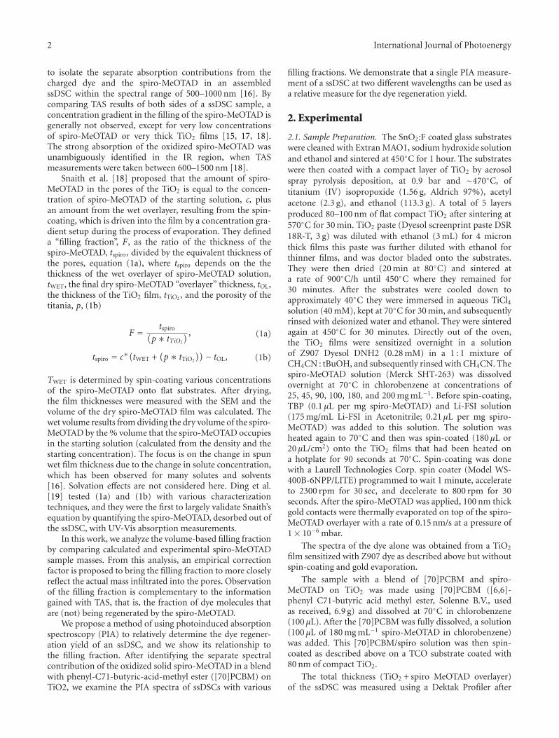
2 International Journal of Photoenergy
to isolate the separate absorption contributions from thecharged dye and the spiro-MeOTAD in an assembledssDSC within the spectral range of 500–1000 nm [16]. Bycomparing TAS results of both sides of a ssDSC sample, aconcentration gradient in the filling of the spiro-MeOTAD isgenerally not observed, except for very low concentrationsof spiro-MeOTAD or very thick TiO2 films [15, 17, 18].The strong absorption of the oxidized spiro-MeOTAD wasunambiguously identified in the IR region, when TASmeasurements were taken between 600–1500 nm [18].
Snaith et al. [18] proposed that the amount of spiro-MeOTAD in the pores of the TiO2 is equal to the concen-tration of spiro-MeOTAD of the starting solution, c, plusan amount from the wet overlayer, resulting from the spin-coating, which is driven into the film by a concentration gra-dient setup during the process of evaporation. They defineda “filling fraction”, F, as the ratio of the thickness of thespiro-MeOTAD, tspiro, divided by the equivalent thickness ofthe pores, equation (1a), where tspiro depends on the thethickness of the wet overlayer of spiro-MeOTAD solution,tWET, the final dry spiro-MeOTAD “overlayer” thickness, tOL,the thickness of the TiO2 film, tTiO2 , and the porosity of thetitania, p, (1b)
F = tspiro(p ∗ tTiO2
) , (1a)
tspiro = c∗(tWET +
(p ∗ tTiO2
))− tOL, (1b)
TWET is determined by spin-coating various concentrationsof the spiro-MeOTAD onto flat substrates. After drying,the film thicknesses were measured with the SEM and thevolume of the dry spiro-MeOTAD film was calculated. Thewet volume results from dividing the dry volume of the spiro-MeOTAD by the % volume that the spiro-MeOTAD occupiesin the starting solution (calculated from the density and thestarting concentration). The focus is on the change in spunwet film thickness due to the change in solute concentration,which has been observed for many solutes and solvents[16]. Solvation effects are not considered here. Ding et al.[19] tested (1a) and (1b) with various characterizationtechniques, and they were the first to largely validate Snaith’sequation by quantifying the spiro-MeOTAD, desorbed out ofthe ssDSC, with UV-Vis absorption measurements.
In this work, we analyze the volume-based filling fractionby comparing calculated and experimental spiro-MeOTADsample masses. From this analysis, an empirical correctionfactor is proposed to bring the filling fraction to more closelyreflect the actual mass infiltrated into the pores. Observationof the filling fraction is complementary to the informationgained with TAS, that is, the fraction of dye molecules thatare (not) being regenerated by the spiro-MeOTAD.
We propose a method of using photoinduced absorptionspectroscopy (PIA) to relatively determine the dye regener-ation yield of an ssDSC, and we show its relationship tothe filling fraction. After identifying the separate spectralcontribution of the oxidized solid spiro-MeOTAD in a blendwith phenyl-C71-butyric-acid-methyl ester ([70]PCBM) onTiO2, we examine the PIA spectra of ssDSCs with various
filling fractions. We demonstrate that a single PIA measure-ment of a ssDSC at two different wavelengths can be used asa relative measure for the dye regeneration yield.
2. Experimental
2.1. Sample Preparation. The SnO2:F coated glass substrateswere cleaned with Extran MAO1, sodium hydroxide solutionand ethanol and sintered at 450◦C for 1 hour. The substrateswere then coated with a compact layer of TiO2 by aerosolspray pyrolysis deposition, at 0.9 bar and ∼470◦C, oftitanium (IV) isopropoxide (1.56 g, Aldrich 97%), acetylacetone (2.3 g), and ethanol (113.3 g). A total of 5 layersproduced 80–100 nm of flat compact TiO2 after sintering at570◦C for 30 min. TiO2 paste (Dyesol screenprint paste DSR18R-T, 3 g) was diluted with ethanol (3 mL) for 4 micronthick films this paste was further diluted with ethanol forthinner films, and was doctor bladed onto the substrates.They were then dried (20 min at 80◦C) and sintered ata rate of 900◦C/h until 450◦C where they remained for30 minutes. After the substrates were cooled down toapproximately 40◦C they were immersed in aqueous TiCl4solution (40 mM), kept at 70◦C for 30 min, and subsequentlyrinsed with deionized water and ethanol. They were sinteredagain at 450◦C for 30 minutes. Directly out of the oven,the TiO2 films were sensitized overnight in a solutionof Z907 Dyesol DNH2 (0.28 mM) in a 1 : 1 mixture ofCH4CN : tBuOH, and subsequently rinsed with CH4CN. Thespiro-MeOTAD solution (Merck SHT-263) was dissolvedovernight at 70◦C in chlorobenzene at concentrations of25, 45, 90, 100, 180, and 200 mg mL−1. Before spin-coating,TBP (0.1 μL per mg spiro-MeOTAD) and Li-FSI solution(175 mg/mL Li-FSI in Acetonitrile; 0.21 μL per mg spiro-MeOTAD) was added to this solution. The solution washeated again to 70◦C and then was spin-coated (180 μL or20 μL/cm2) onto the TiO2 films that had been heated ona hotplate for 90 seconds at 70◦C. Spin-coating was donewith a Laurell Technologies Corp. spin coater (Model WS-400B-6NPP/LITE) programmed to wait 1 minute, accelerateto 2300 rpm for 30 sec, and decelerate to 800 rpm for 30seconds. After the spiro-MeOTAD was applied, 100 nm thickgold contacts were thermally evaporated on top of the spiro-MeOTAD overlayer with a rate of 0.15 nm/s at a pressure of1× 10−6 mbar.
The spectra of the dye alone was obtained from a TiO2
film sensitized with Z907 dye as described above but withoutspin-coating and gold evaporation.
The sample with a blend of [70]PCBM and spiro-MeOTAD on TiO2 was made using [70]PCBM ([6,6]-phenyl C71-butyric acid methyl ester, Solenne B.V., usedas received, 6.9 g) and dissolved at 70◦C in chlorobenzene(100 μL). After the [70]PCBM was fully dissolved, a solution(100 μL of 180 mg mL−1 spiro-MeOTAD in chlorobenzene)was added. This [70]PCBM/spiro solution was then spin-coated as described above on a TCO substrate coated with80 nm of compact TiO2.
The total thickness (TiO2 + spiro MeOTAD overlayer)of the ssDSC was measured using a Dektak Profiler after

International Journal of Photoenergy 3
a scratch with a scalpel was made in the nonactive regionbetween the gold contacts.
2.2. IV Measurements. Current-voltage measurements of thessDSC were performed using a continuous solar simulator(Wacom) with a 5 kW Xe lamp (Type WXS-300S-50). Themeasurements were performed at STC (Standard Test Con-ditions: 1000 W m−2, 25◦C and AM1.5 spectrum, inclusive ofa spectral mismatch correction, designed for the liquid DSCwith Z907, utilizing a monocrystalline silicon solar cell withKG3 filter (Fraunhofer ISE RS-ID 2)) using a home-mademeasurement system which included a Keithley 2400 Sourcemeter. The mismatch factor was not tailored to the ssDSC.Our experience with Z907 informs us of an error of about5%.
2.3. Desorption Measurements. UV-Vis spectra were takenusing a HP 8453 spectrometer and cuvettes from Hellma type117.100-QS. The area of the cut samples was determinedwith the aid of a computerized optical microscope (LeicaMZ7.5 Microsystems). Desorption of the samples was donein a closed flask filled with a known volume of chlorobenzenefor 1 hour.
2.4. Density of Spiro-MeOTAD. A quartz cuvette with anopening of 4 × 10 mm was filled to the rim with water todetermine the total inner volume of the cuvette. The volumewas calculated by subtracting the weight of the full cuvettewith that of the empty cuvette. To determine the volume ofspiro-MeOTAD, this procedure was done on both an emptycuvette and a cuvette containing spiro-MeOTAD. After thevolume of the empty cuvette was determined, the cuvette wasfilled with a 200 mg/mL spiro solution and heated to 70◦Cfor 24 hours to evaporate the chlorobenzene. The weight ofthe spiro-MeOTAD was then determined by subtracting theweight of the cuvette before and after it was filled with spiroMeOTAD.
2.5. Photoinduced Absorption. Near steady-state photoin-duced absorption spectra were recorded between 0.5 and2.5 eV by excitation at 458 (2.71 eV) or 514 nm (2.41 eV)with a mechanically modulated (275 Hz) continuous waveargon ion laser pump beam and by measuring the changein transmission of a tungsten-halogen probe beam throughthe sample (ΔT) with a phase sensitive lock-in amplifierafter dispersion with a monochromator and detectionusing Si, InGaAs, and cooled InSb detectors. The pumppower was typically 50 mW with a beam diameter of2 mm. The signal intensity (ΔT T−1) was corrected forthe photoluminescence, which was recorded in a separateexperiment. Samples were measured in ambient atmo-sphere (290 K). The error is estimated to be <5%, butdepends on the signal intensity and the transmission ofthe sample. Any error in the overlap of the beams iscancelled out by dividing the signals taken at differentwavelengths.
Overlayer of spiro-MeOTAD
Sample 27
Sample 27
ECN SEI 1μm WD15 mm
SnO2:F
15 kV x25,000
Figure 1: SEM cross-section of a ssDSC: the overlayer of the spiro-MeOTAD is visible on the top of the TiO2 film.
3. Results and Discussion
3.1. SEM Characterization and Filling Fraction Analysis. Atypical example of an ssDSC cross-section is shown inFigure 1. The SnO2 : F layer on the conducting glass isclearly visible. The degree of the penetration of the spiro-MeOTAD into the TiO2 is visually often not apparent andthe composite often appears as a monolithic layer. The spiro-MeOTAD overlayer however is evident and measurable inthe SEM image. ssDSC cross-sections showing a range ofoverlayer thicknesses are shown in Figure 2. The imagesA and B in Figure 2 have relatively thick spiro-MeOTADoverlayers, with visible striations apparently produced in thespin-coating process step. While the upper edge in Image Cof Figure 2 is smooth, it is not resolvable whether there isa continuous spiro-MeOTAD overlayer or not. The existenceof this layer was only deduced by the electrical measurementsdescribed below. The topmost edge of the sample in ImageD appears to have a rougher surface, with particles clearlyvisible, indicating that there is no overlayer present, or thatthe overlayer may be shortened by the particles sticking up.
In order to calculate the filling fraction in (1a) and(1b), the thicknesses of the spiro-MeOTAD overlayer andof the TiO2 film were measured by SEM. The porosity wastaken to be 68% [19], which is typical for unsensitizedTiO2 films. The influences on the porosity due to samplevariation, the presence of the dye, double layer or solvationeffects, were not taken into account here. The focus is toidentify the influential parameters and the trends observedin the pore filling due to the variation of spiro-MeOTADconcentration. Figure 3 shows the range of filling fractions,as calculated using (1a) and (1b), plotted as a function of theconcentration of spiro-MeOTAD in solution, for the ssDSCsamples in this study. The relationship of tWET to the spiro-MeOTAD concentration is plotted in Figure 4(a).
3.2. I-V Characteristics. The short circuit currents and fillfactors are plotted in Figure 4(b) for some samples withspiro-MeOTAD concentrations of 100 and 200 mg mL−1.Cells having no overlayer (as for all samples with
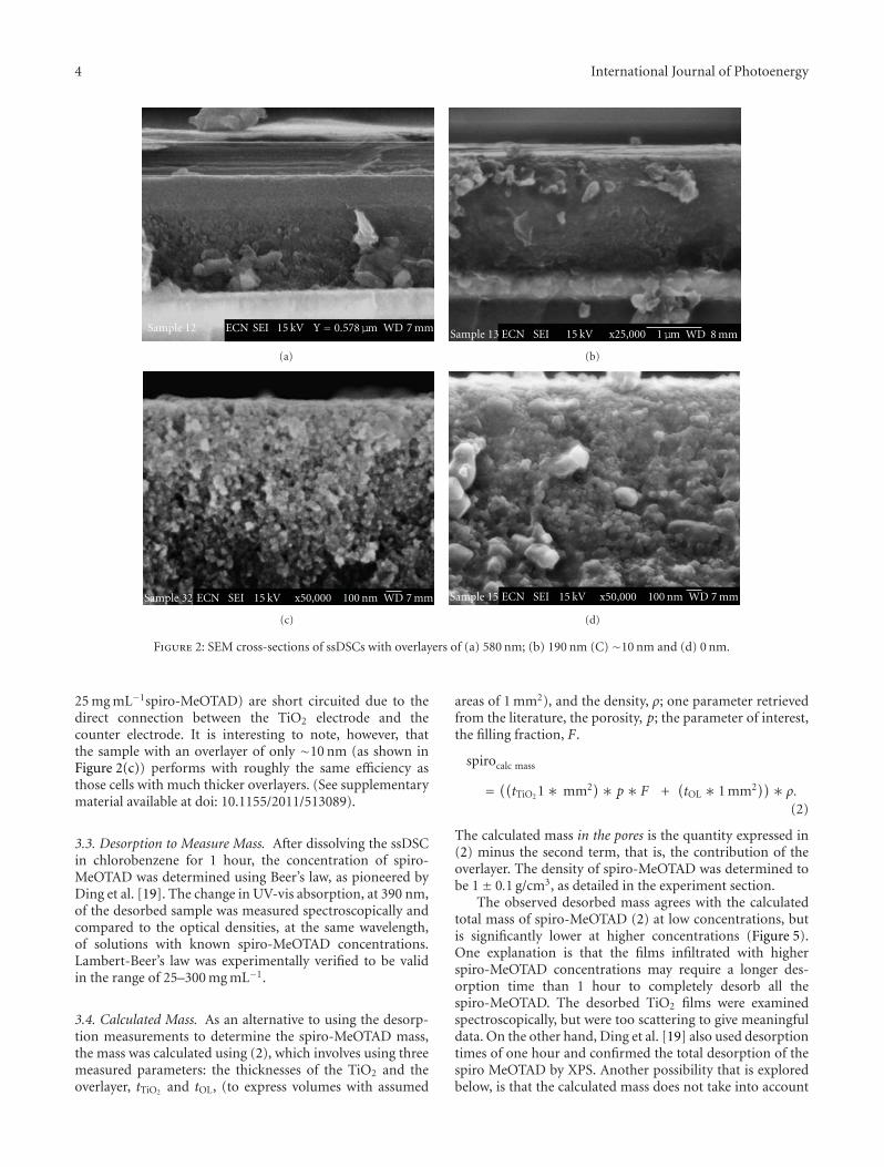
4 International Journal of Photoenergy
ECN SEI WD 7 mm15 kV Y = 0.578μmSample 12
(a)
ECN SEI 1μm WD 8 mm15 kV x25,000Sample 13
(b)
ECN SEI WD 7 mm100 nm15 kVSample 32 x50,000
(c)
ECN SEI WD 7 mm100 nm15 kV x50,000Sample 15
(d)
Figure 2: SEM cross-sections of ssDSCs with overlayers of (a) 580 nm; (b) 190 nm (C) ∼10 nm and (d) 0 nm.
25 mg mL−1spiro-MeOTAD) are short circuited due to thedirect connection between the TiO2 electrode and thecounter electrode. It is interesting to note, however, thatthe sample with an overlayer of only ∼10 nm (as shown inFigure 2(c)) performs with roughly the same efficiency asthose cells with much thicker overlayers. (See supplementarymaterial available at doi: 10.1155/2011/513089).
3.3. Desorption to Measure Mass. After dissolving the ssDSCin chlorobenzene for 1 hour, the concentration of spiro-MeOTAD was determined using Beer’s law, as pioneered byDing et al. [19]. The change in UV-vis absorption, at 390 nm,of the desorbed sample was measured spectroscopically andcompared to the optical densities, at the same wavelength,of solutions with known spiro-MeOTAD concentrations.Lambert-Beer’s law was experimentally verified to be validin the range of 25–300 mg mL−1.
3.4. Calculated Mass. As an alternative to using the desorp-tion measurements to determine the spiro-MeOTAD mass,the mass was calculated using (2), which involves using threemeasured parameters: the thicknesses of the TiO2 and theoverlayer, tTiO2 and tOL, (to express volumes with assumed
areas of 1 mm2), and the density, ρ; one parameter retrievedfrom the literature, the porosity, p; the parameter of interest,the filling fraction, F.
spirocalc mass
= ((tTiO2 1∗ mm2)∗ p ∗ F +(tOL ∗ 1 mm2))∗ ρ.
(2)
The calculated mass in the pores is the quantity expressed in(2) minus the second term, that is, the contribution of theoverlayer. The density of spiro-MeOTAD was determined tobe 1± 0.1 g/cm3, as detailed in the experiment section.
The observed desorbed mass agrees with the calculatedtotal mass of spiro-MeOTAD (2) at low concentrations, butis significantly lower at higher concentrations (Figure 5).One explanation is that the films infiltrated with higherspiro-MeOTAD concentrations may require a longer des-orption time than 1 hour to completely desorb all thespiro-MeOTAD. The desorbed TiO2 films were examinedspectroscopically, but were too scattering to give meaningfuldata. On the other hand, Ding et al. [19] also used desorptiontimes of one hour and confirmed the total desorption of thespiro MeOTAD by XPS. Another possibility that is exploredbelow, is that the calculated mass does not take into account

International Journal of Photoenergy 5
0
20
40
60
80
100
Filli
ng
frac
tion
(%)
Spiro-MeOTAD concentration (mg mL− 1)
0 50 100 150 200
Figure 3: Filling fraction versus spiro-MeOTAD concentration, cal-culated according (1a) and (1b), for samples with TiO2 thicknessesof: 1.4 μm (�); 1.7 μm (•); 2 μm (�); 3 μm (�); 5 μm (�).
the effect of increased viscosity at higher spiro-MeOTADsolution concentrations, which lowers the capillary force todraw the liquid into the oxide matrix (see (6) below).
3.5. Characteristic Penetration Length. By multiplying thefilling fraction by the thickness of the TiO2 film, a charac-teristic penetration length (CPL) may be determined:
CPL = F ∗ tTiO2 . (3)
The term “characteristic penetration length” may suggestthat the solution penetrates the film from top to bottom,infiltrating all the porous spaces equally, but this is notrealistic considering the experimental evidence that thereis typically no concentration gradient across the ssDSC[15, 17, 18]. The TiO2 particulate film is composed ofpores of various diameters which randomly branch andneck, and the primary infiltration mechanism is thoughtto be capillary action [19], which depends on the porediameter. Nevertheless, it is a way of comparing the relativefilling of one film with another. The CPL is found tobe a constant, for all ssDSCs of a given spiro-MeOTADconcentration, independent of film thickness. (Please seesupporting information for electrical characteristics.)
The mass, m, is related to the CPL through (4), using thevolume (area, A, times length, CPL), porosity, p, and density,ρ.
m = A∗ CPL∗ ρ ∗ p
= 1 mm2 ∗ (tTiO2 ∗ F)∗ ρ∗ p.
(4)
Equation (4) is the same as (2) minus the overlayer. InFigure 5, the experimentally desorbed mass (which includesthe overlayer) for ssDSCs of different spiro-MeOTAD con-centrations are compared to the calculated total mass, aswell as the calculated mass in the pores (or equivalently, the
CPL times porosity). The filling fraction used in the calcu-lated quantities overestimates the mass of spiro-MeOTADinfiltrated in the pores. (Equivalently, we could have usedthe desorbed mass (see supplementary materials) and (2)to compare empirical filling fractions to filling fractionscalculated with (1a) and (1b), with the latter similarlyoverestimating the experimental.) While the filling fractionallows for variations in wet overlayer thicknesses, tWET, itdoes not account for the effect of viscosity on the capillaryinfiltration force. Therefore a correction based on viscosity isproposed to bring the CPL, and the filling fraction, F, morein line with the observed desorbed mass.
The relationship between tWET and the spiro-MeOTADconcentration is an exponential one, as shown in Figure 4(a),suggesting that the higher concentrations have a higherviscosity, requiring more centrifugal force to be spun off thanlower concentrations of spiro-MeOTAD. The film thickness,as determined by spin-coating at a fixed speed, is a balancebetween the drying rate and the radial shear force on thesolution. The viscosity of the solution is the resistance ofthe solution to deformation by the shear force. For manymaterials, up to concentrations of 50%, the viscosity ofsolution increases for higher concentrations of solute [16].The results show that spiro-MeOTAD in chlorobenzene alsofollows this trend.
An empirical correction factor may be proposed toaccount for the exponentially thicker layer at higher con-centrations. Extrapolating the exponential function to aconcentration of 0 mg mL−1 gives a tWET0 of 3.5 microns, thevalue at which the CPL-based calculation agrees well withthe calculated mass. The data shows that an increase in theviscosity with concentration has an inverse impact on thepenetration length. Therefore the CPL may be adjusted withthe ratio of tWET0/tWET to account for this effect. Indeed, animproved characteristic length which is more in line withthe experimental results is obtained, as indicated in (5), andplotted in Figure 5
CPLcorr = CPL∗ tWET0
tWET, Fcorrected = F ∗ tWET0
tWET. (5)
This may be useful to estimate the extent of filling ofspiro-MeOTAD in the pores of a TiO2 nanoparticulate film.The penetration of a solution into a wetted capillary, orporous medium, is described by the Lucas-Washburn [20–22] equation, in which � is the penetration length, reff is theeffective hydrodynamic pore radius, γ is the surface tension,η is the viscosity, θ is the contact angle, and t is the time, asgiven in (4)
l2 =(γ
η
cos θ2
)refft. (6)
Equation (6) shows that the penetration length is a functionof the viscosity of the penetrating solution. The applicationof this equation requires a determination of the effectiveradius in the tortuous particulate TiO2 film, which, forexample, has been performed for alumina packed beds [21].It clearly shows the relationship of viscosity to penetrationlength and may be the focus of future work in understanding

6 International Journal of Photoenergy
t WE
T(μ
m)
5
4.5
3.550 100 150 200
4
Spiro-MeOTAD concentration (mg mL−1)
tWET = 0.07∗ exp(x/68.9) + 3.5
(a)
Overlayer thickness (μm)
= 2.1%
= 2.2% = 2.2%
= 2.3%
= 1.7%
Fill
fact
or(%
)
4
5
6
7
0 0.1 0.2 0.3 0.4 0.5 0.6
0.45
0.55
3
0.6
0.5
J sc(
Acm
−1)
(b)
Figure 4: (a) Wet layer thickness (tWET) as a function of the spiro-MeOTAD concentration, fitted with an exponential. (b) Shortcircuit currents (squares) and fill factors (circles) for ssDSCs as a function of spiro-MeOTAD overlayer thicknesses, for spiro-MeOTADconcentrations of 100 mg mL−1 (open symbols) and of 200 mg mL−1 (closed symbols).
0 50 100 150 200
Spiro-MeOTAD concentration (mg mL−1)
Ch
arac
teri
stic
pen
etra
tion
len
gth
(μm
)∗po
rosi
ty
Des
orbe
dm
ass
(μg)
0
0.5
1
1.5
2
0
0.5
1
1.5
2
Figure 5: The scale of the CPL (μm), times the porosity (%), is thesame as the one for the desorbed mass (μg) for spiro-OMeTAD witha density of 1 g/cm3 (see text). Average calculated and experimentalvalues of the mass are plotted versus spiro-MeOTAD concentration.The experimentally determined mass desorbed from the samples(�) is much lower than the calculated total mass (�) and shouldbe greater than the calculated mass in the pores (�) becausethe former also includes the overlayer. The uncorrected CPL (•)is equal to the calculated mass in the pores (�). These valuesindicate that the filling fraction overestimates the amount of spiro-MeOTAD which actually infiltrates the pores. The correction forviscosity effects (©) for higher concentrations of spiro-MeOTADgives an improved value for the CPL, or calculated mass in the pores.(The standard deviation of all CPL and desorbed mass values is<0.12 μm.)
and optimizing the infiltration of a hole conductor intoa TiO2 film. Understanding the pore filling mechanismreflected by the filling fraction is a key to optimizing the porefilling. References to the CPL in this paper from this point on
will refer to the CPLcorr, which is corrected for the effects ofviscosity.
3.6. Photoinduced Absorption Spectroscopy: Relation to FillingFraction. The photoinduced absorption spectroscopy tech-nique allows optical detection of excited species generatedby photoexcitation, such as the oxidized states of the dye,Z907, and the hole conductor, spiro-MeOTAD, in a ssDSC.After injection of the electron by the dye into the conductionband of the TiO2, the dye cation is normally regenerated toits neutral state by an electron from the spiro-MeOTAD aftera period ranging from less than ps to greater than ns [6]. Inthe absence of a hole conductor, an electron from the TiO2
recombines with the oxidized dye cation after a period ofhundreds of microseconds [2], during which the absorptionspectrum of the oxidized dye may be observed.
When spiro-MeOTAD perfectly infiltrates the sensitizedTiO2 film and regenerates the dye, the photoinducedabsorption features of the oxidized dye are replaced withthat of oxidized spiro-MeOTAD [6, 7, 15, 17, 18]. Inthe extended visible spectral range (400–1000 nm), manysignals may overlap due to contributions of the oxidized dye(absorption and bleaching bands) [23], electrons in TiO2
[24, 25], and oxidized spiro-MeOTAD [18]. This confluenceof signals in the visible region makes it very difficult toanalyze spectra. Even when the separate spectral featuresof the oxidized dye and spiro-MeOTAD are known, nearsteady state photoinduced absorption spectra in the spectralrange of 400–1000 nm cannot always be fitted with a linearaddition of the independent oxidized dye or hole-conductor,because the electron density of the TiO2 surface may leadto spectral shifts in the ground state absorption of dyes andthereby to additional spectral variations near the bleachingband [17]. Alternatively, the observation window may beextended to the near infrared region of the spectrum, where
International Journal of Photoenergy 7
oxidized spiro-MeOTAD shows a broad absorption band andthe oxidized ruthenium dyes do not absorb. This strategywas used by Snaith et al. in a qualitative analysis of theirphotoinduced absorption spectra [18].
The PIA spectrum of only the dye Z907 on TiO2 revealsa positive ΔTT−1 signal (i.e., bleaching) with a maximumat 515 nm, and a negative signal (i.e., absorption) peakingbetween 750–800 nm. (Figure 6(a)). The spectral shape isvery similar to that reported for TiO2 films sensitizedwith the well-studied and structurally similar dyes N3(cis-Ru(dcbpy)2(NCS)2) [12–14, 26] and N719 (its bis-deprotonated analog) [27]. Therefore, we can safely attributethe positive signal to the bleaching band of Z907 and thenegative signal to the absorption band of oxidized Z907.Additionally, a weak absorption tail of electrons in TiO2
− ispresent in the visible to near infrared region [24, 25].
Although steady-state spectra of chemically oxidizedspiro-MeOTAD in solution [28, 29] as well as spectroelectri-cal studies [29] of spiro-MeOTAD in TiO2 films are available,spectral near steady-state PIA features of optically oxidizedspiro-MeOTAD in the solid state may provide slightlydifferent absorption features. Therefore [70]PCBM was usedas a photosensitizer to generate a photoinduced absorptionspectrum (Figure 6(a)) of oxidized spiro-MeOTAD in asolid composite blend with [70]PCBM on TiO2 and in theabsence of dye Z907. [70]PCBM is used because it can bephotoexcited and accept electrons from spiro-MeOTAD [29–31], as a result of its strong ground state absorption in thevisible region and strong electron accepting properties [32].The PIA spectrum of the [70]PCBM:spiro-MeOTAD mixturein TiO2 reveals two absorption bands in the visible region atca. 515 nm (2.41 eV) and 700 nm (1.68 eV), and one in thenear infrared at 1500 nm (0.83 eV) as shown in Figure 6(a).These three bands are attributed to oxidized spiro-MeOTAD,because of good agreement with previously reported spectrathat were obtained by stepwise chemical oxidation [28, 29]or in spectroelectrical studies [29, 33]. In dichloromethanesolution, Struijk found two absorption bands in the visible, astrong band at 521 nm and a less intense band at 678 nm, andone in the near infrared, at 1514 nm, after stepwise chemicaloxidation [28] A 5–25 nm shift is typically observed whencomparing the spectra of a photoactive species in solution toone in the solid state and is due to molecular interaction withthe local environment.
Having established the separate contributions of oxidizedZ907 and spiro-MeOTAD, it is possible to analyze PIA spec-tra of TiO2 films containing both Z907 and spiro-MeOTAD.For ssDSCs, the PIA spectrum strongly changes with increas-ing spiro-MeOTAD concentration from 25 to 180 mg mL−1
(Figure 6(b)). For the lowest concentration, the absorptionmaximum at 780 nm and the presence of a bleaching bandbelow 600 nm (Figure 6(b)) are signatures of oxidized Z907.Contributions of oxidized spiro-MeOTAD are visible fromthe band at 1450 nm, and from its absorption between 550and 800 nm. This latter absorption peak overlaps with thebleaching band of the dye and thereby causes an altered formof the positive ΔTT−1 band below 600 nm, as comparedto the dyed film without spiro-MeOTAD (Figure 6(a)). Forthe highest concentration of spiro-MeOTAD the absorption
maxima of the bands are 515, 730, and 1450 nm, in goodcorrespondence to the spectrum obtained for the filmusing [70]PCBM as photosensitizer. This indicates that atthe highest concentration, the major part of the dye isregenerated by spiro-MeOTAD. However, comparison of thespectrum of the ssDSC, with 180 mg mL−1 spiro-MeOTAD,with that of the spiro-MeOTAD/PCBM blend (Figure 6(c))shows that even for the highest concentration of spiro-MeOTAD (triangles), there is still some oxidized dye present(visible by the bleaching band at 565 nm and the additionalabsorption around 750 nm). Furthermore, the additionalabsorption in the region 850–1200 nm may be explained withthe absorption of free electrons in TiO2 [24].
Overall, with increasing spiro-MeOTAD concentration,two major spectral changes occur: (1) between 750 and850 nm the ΔTT−1 signal intensity reduces (relative to the1450 nm peak) and (2) between 525 and 600 nm the positive(i.e., bleaching) signal turns into a negative (i.e., absorption)signal (Figure 6(b)). With increasing spiro-MeOTAD con-tent, both absorption changes are due to lower contributionof the strong absorption (around 800 nm) and bleaching(around 565 nm) of oxidized Z907, relative to oxidized spiro-MeOTAD. By plotting the absorbance at 565 nm versus thatat 825 nm, as in Figure 7(a), a linear relation is found withincreasing spiro-MeOTAD concentration, when the spectrais normalized at the spiro-MeOTAD 1450 nm peak. Thisindicates that the spectral changes are due to the samephotoexcited species, which we conclude is the oxidized dye.
Plotting all the data gives a slope of −2.0, but thePIA signal (ΔTT−1) of those samples with the lowestconcentration of spiro-MeOTAD are much more scatteringthan the rest of the samples. They are a bilayer, in whichthe effective refractive index of one layers is the average ofspiro-MeOTAD, TiO2 and air and the other layer is onlyan average of TiO2 and air, and is consistent with otherobservations of concentration gradients in samples withlow concentrations of spiro-MeOTAD [17]. These samplesclearly scatter the light differently than a single compositelayer of spiro- MeOTAD, TiO2 and air. Highly scatteringsamples may dramatically influence the accuracy of the PIAmeasurement by lowering the magnitude of both ΔT andT−1, introducing a large error in their ratio. When thesepoints are disregarded, the linear fit has a slope of −2.2. Aline with a slope of −2.4 is also plotted to show that thisslope is also within the accuracy of the measurement and/orthe fit. A slope of −2.4 is expected because the ratio of PIAsignal intensities at 565 nm to 825 nm for the dye on TiO2
alone, without spiro-MeOTAD, is −2.4. (Figure 6(a)). Theratio of the dye cation absorption peak at 825 nm, or at565 nm, to the spiro-MeOTAD cation peak at 1450 may beused to extract the relative dye cation concentration from theabsorption spectrum of the ssDSC.
The PIA signal intensities for the 565 nm and 825 nmpeaks, relative to the 1450 nm spiro-MeOTAD peak, areplotted as a function of filling fraction in the inset ofFigure 7(b). Because the filling fraction is a nondimensionalmeasure of concentration, it has an exponential relationshipto the transmitted light intensity, as predicted by theBeer-Lambert law, given in (7), where I is intensity, εi is

8 International Journal of Photoenergy
2000 1500 1000 800 700 600 500
1
0
-1
1 1.5 2 2.5
Wavelength (nm)
Energy (eV)
Spiro-MeOTAD cation absorption
Dye bleach
×40Z907 dye cation absorption
−ΔT/T
(×10
3)
(a)
2000 1500 1000 800 700 600 500
1
0
-1
1 1.5 2 2.5
Wavelength (nm)
Energy (eV)
Nor
mal
ized
ΔT/T
(b)
2000 1500 1000 800 700 600 500
1
0
1 1.5 2 2.5
Wavelength (nm)
Energy (eV)
Nor
mal
ized
ΔT/T
Dye bleach
Normalized spiro cation peak
Dye cation absorption
Spiro cation
ssDSC with high conc
ro
[70]PCBM + spiro
(c)
100 1000
ΔT
(a.u
.)
Frequency (Hz)
1E− 3
1E− 4
1E− 5
45 mg mL−1 spiro180 mg mL−1 spiro
(d)
Figure 6: Photoinduced absorption spectra of (a) dye Z907 in TiO2 (©), and [70]PCBM blended with spiro-MeOTAD on TiO2 (�,multiplied with a factor of 40); (b) TiO2 sensitized with dye Z907, with spiro-MeOTAD, normalized at the peak at 1400–1500 nm (0.83–0.89 eV), using spiro-MeOTAD concentrations of 25 (�),45 (•), 90 (�), and 180 (�) mg mL−1; (c) spectrum of a ssDSC: sensitized(Z907) TiO2 infiltrated with a high concentration of spiro-MeOTAD (200 mg mL−1), (�); compared with the spectrum of the spiro-MeOTAD/PCBM blend, (�). Spectra were recorded using excitation wavelengths of 514 nm (a, c) and 458 nm (b, c). (d) Frequency-dependent PIA intensities for TiO2 samples sensitized with dye Z907, infiltrated with 45 (�) or 180 (�) mg mL−1 spiro-MeOTAD solution.The measurements were recorded at 1.05 eV (1180 nm). The solid lines are fits to the data (13) and result in steady-state lifetimes of 115 and995 μs for the low and the high spiro-MeOTAD concentration, respectively.
the extinction coefficient of species i, ci is the concentrationof species i and l is path lengt.
log(I0
I
)=∑
εici l
= εdye cation cdye cation l + εspiro MeOTAD cspiro MeOTADl.
(7)
Normalizing the data at the spiro-MeOTAD peak at 1450 hastwo effects: (i) the observed signal at the 825 nm peak is nowa ratio of the signals at the 825 and 1450 nm peaks and (ii)the expression (ε1450
spiro+ ∗ c1450spiro+ ∗ l) is set to a magnitude of
one. The Beer-Lambert law for the normalized data may bewritten as shown in (8) and simplified with the introduction
of constants for the ratio of the extinction coefficients for therespective peaks, as shown in (9)
log (ΔI)825
log (ΔI)1450
=(ε825
spiro+cspiro+ l + ε825dye+cdye+ l
)ε1450
spiro+cspiro+ l
=ε825
spiro+
ε1450spiro+
+ε825
dye+cdye+ l
ε1450spiro+cspiro+ l
(8)
International Journal of Photoenergy 9
−1.5
−1.25
−1
−0.75
−0.25
0
0.25
0.7 0.8
y= 0.5− 2.2∗ x
0.5
−0.5
0.20.1 0.3 0.4 0.5 0.6
Relative ΔTT−1 (825 nm/1450 nm)
(565
nm
/145
0n
m)
Rel
ativ
eΔTT−1
(a)
1.2
0.4
0.4
0.6
0
0
0
0.05
0.15
0.25
0.35
0.1
0.20.2
0.30.8
2 4 6 8 10×10−5
PIA
sign
al
F(%)
−ln
(PIA
45m
g/m
L@82
5n
m)/
2.3
c∗/(mol cm L−1)
(b)
Figure 7: (a) ΔTT−1 signal intensities relative to the peak at 1450 nm, for 565 nm ((ΔT565 nmT565 nm−1)/(ΔT1450 nmT1450 nm
−1), y-axis)compared to 825 nm ((ΔT825 nmT825 nm
−1)/(ΔT1450 nmT1450 nm−1), x-axis). The solid line is a linear fit to the data, excluding the highly
scattering points at the lowest concentration: y = −2.2x + 0.5. The dashed line shows y = −2.4 x + 0.55. (b) The ln(relative PIAsignal at 825 nm)/2.3 is plotted against the concentration times length (mol cm L−1). The spiro-MeOTAD concentrations are 45 (�), 90(�), 100 () mg mL−1; 180 (©) mg mL−1; 200 (�) mg mL−1. Inset: ΔTT−1 signal intensity relative to the peak at 1450 nm, for 825 nm((ΔT825 nmT825 nm
−1)/(ΔT1450 nmT1450 nm−1), �) and for 565 nm ((ΔT565 nmT565 nm
−1)/(ΔT1450 nmT1450 nm−1), () compared to the filling fraction
obtained in Section 2.1. The data are fitted with exponential functions: y = −2∗exp(−x/0.1) + 1.1 (solid line) and−1∗exp(−x/0.1) + 0.75.
= B+A∗(cdye+
cspiro+
), where A =
⎛⎝ ε825dye+
ε1450spiro+
⎞⎠, B =⎛⎝ε825
spiro+
ε1450spiro+
⎞⎠.(9)
If the extinction coefficients and the concentrations of thedye and spiro MeOTAD cations are known, then (9) isquite useful. But, it is also possible to reformulate (8)so that the normalized PIA signal provides a measure ofthe dye cation population, relative to the concentration ofspiro-MeOTAD present, without knowledge of the respectiveextinction coefficients or cation concentrations. It is quiteevident that the dye cation population, that is, those dyes thatare not regenerated by the hole conductor, is related to theconcentration of the hole conductor, and so we can let theratio of the dye cation density to the spiro-cation density bea function of the spiro-MeOTAD concentration, as expressedin (10). Now, a relationship between the normalized PIAsignal and the concentration of spiro-MeOTAD can bewritten using an effective extinction coefficient as shown in(11)
letcdye+
cspiro+= f
(cspiro
)= ξ ∗ cspiro,
let ε′effective =ε825
dye+
ε1450spiro+
∗ ξ
l,
(10)
log (ΔI)825
log (ΔI)1450= B + ε′effective ∗ cspiro ∗ l. (11)
It is interesting to apply (11) to the PIA data, usingthe CPL (i.e., F ∗ tTiO2 ) in (12), to calculate the effectiveextinction coefficient, with units of M−1 cm−1, of the relativeintensity signal at 825 nm, as plotted in Figure 7(b).
cl[
mol cmL
]= ρ
MspiroMeOTAD∗ p ∗ F ∗ tTiO2
= 1000 g/L1230 g/moL
∗ 0.68∗ CPL[μm]∗ cm
104 μm.
(12)
Figure 7(b) shows that the data may be linearly fitted for allconcentrations higher than 25 mg mL−1. The error bars arebased upon the deviation of a group of three measurements,and the line has an intercept of 0.16 ± 0.02 and the slope,−814 ± 120. The slope of this line is the effective extinctioncoefficient for this system. Here, as in the linear fit ofthe optical data plotted in Figure 7(a), the data points forthe very low concentrations of spiro-MeOTAD were notincluded in the linear fit. Furthermore, in the event ofa bi-layer (TiO2 + spiro-MeOTAD + air |TiO2+ air), therelationship between the spiro-MeOTAD concentrations andthe dye and oxidized spirocations, assumed in (10), wouldbreak down. Indeed, as the concentration of spiro-MeOTADapproaches zero, so will the concentration of spiro-MeOTADcation, and the expression for ξ will become undefinedand very near to this singularity, the relationship becomessuperlinear. Despite these considerations, employing thisrelationship is useful for interpreting the data in the rangeof concentrations from 45 mg mL−1 up through at least300 mg mL−1.

10 International Journal of Photoenergy
It is possible to estimate the magnitude of c ∗ l that isnecessary to eliminate the dye cation signal. By extrapolatingthe linear fit in Figure 7(b) to the case where there is nosignal from the dye cation, that is, to y = 0, the abscissa,c ∗ l, is equal to 1.71 × 10⁻⁴ ± 2.6 × 10⁻⁵ M cm, whichcan be converted to a CPL of 3.1 ± 0.46μm using (12).The average (corrected) CPL of the samples with spiro-MeOTAD concentrations of 200 mg mL−1 is 1.4. Comparisonof these two values shows that a doubling of the characteristicpenetration length of spiro MeOTAD is required, thancurrently achieved, in order to be able to regenerate, andthus functionalize, all the dye molecules in a conventionallysensitized ssDSC.
A sample may have a filling fraction of 90% but if the10% of the remaining pore space (i.e., narrow pores) containa third of the dye molecules then the filling is not optimum.Usually high filling fractions can be only achieved withfilms not greater than 2–2.5 microns. Thicker films wouldlead to higher light absorption, higher currents, and higherefficiencies. Indeed, the liquid electrolyte DSC’s are routinelymade to be 8–10 microns thick. Equation (6) shows that thepenetration depth of the capillary force depends on viscosity,wetting and the pore radius. (We can assume, as did Snaithet al. [18] that the chlorobenzene completely wets the TiO2.)In this case, optimization of the pore filling should addressthe viscosity of the concentrated spiro-MeOTAD and/or theeffective pore radius of the TiO2 film, to optimize the amountof spiro-MeOTAD which can infiltrate into the pores bycapillary action.
The PIA measurements in this work were made ata frequency of 275 Hz, very near the crossover point ofthe two curves in Figure 6(d), at which there is littlevariation of signal intensity with spiro MeOTAD concen-tration, and appropriate for a measurement relative to aconstant spiro MeOTAD contribution and the analysis usedabove. However, to quantitatively determine the numberof [non]regenerated cations, or the HTY, the extinctioncoefficients of the two species must be independently known,and the effect of lifetime upon the measurement mustbe taken into account. The magnitude of the PIA signalis proportional to g, the efficiency of generation of thephotoinduced species; I , the pump intensity; τs the lifetimeof a photoexcitation under steady-state conditions, and α =(2vτs)−1.
− ΔT ∝ gIτsα tanhα(α + tanhα)
. (13)
This equation can be used to detect τs from chopperfrequency-dependent PIA measurements. This results insteady-state lifetimes of τs = 115μs for a low spiro-MeOTADconcentration of 45 mg mL−1 and to τs = 995μs for a fourtimes higher spiro-MeOTAD concentration. Such nonequallifetimes with different hole conductor concentrations com-plicate quantitative determination of hole transfer yieldsusing near steady-state photoinduced absorption spectra,because the lifetimes are shorter than the period of the chop-per (ν−1 = 3.6 ms). In this case, an increase in lifetime leadsto an increase in PIA intensity. For lifetime-independentand hence more quantitative detection using near-state PIA
measurements, much higher frequencies would be required.For example, when measuring at 10 kHz, an increase inlifetime from 0.1 to 1 ms would lead to an increase inPIA intensity as a result of the increased lifetime of only4%.
This analysis shows that a single PIA measurement at twodifferent wavelengths (825 nm and 1450 nm) can be used as ameasure for the hole transfer yield (HTY). Furthermore, thismethod is more robust than the previous method describedby Kroeze et al. [15] In that the quantification may beobtained from a single measurement set, therefore it is notnecessary to measure the ssDSC before and after filling withthe hole conductor which requires that the light intensitiesand sample repositioning must be as identical as possible.
4. Conclusions
We prepared ssDSCs with a range of TiO2 thicknessesand filling fractions. The calculated mass based on thefilling fraction, as proposed by Snaith, was greater thanthe experimentally desorbed mass. Because the effects ofviscosity were observed in the thicknesses of the spiroMeOTAD films spun on flat substrates, a correction factorwas proposed for the filling fraction to account for the effectsof viscosity in capillary infiltration. According to the Beer-Lambert law, it was shown that PIA signal is related to thefilling fraction, and the CPL, through an effective extinctioncoefficient, which was determined for this material system,allowing the relative dye cation density to be deduced. Theoptimum value of the CPL, for the sample range of 1.4to 5 μm investigated here, was determined to be 3.1 ± 0.46microns which is roughly double the average CPL for thesamples used in this study (see supplementary material). Thissuggests that a solution with a higher concentration of holeconductor and a lower viscosity and/or a greater effectivepore radius in the TiO2 film is necessary to minimize thethickness of the overlayer, increase the penetration lengthof the spiro-MeOTAD and to optimally functionalize all thedye molecules in an ssDSC. In other words, for the solidelectrolyte to achieve the same intimate contact with the dyemolecules as a liquid electrolyte, the infiltration conditionsmust be engineered so that a more concentrated solution willenter the pores, either by altering the viscosity of the spiro-MeOTAD solution and/or by altering the pore radii of theTiO2 film.
Acknowledgments
The authors kindly acknowledge Professor Dr. Rene Janssen(TU/e) for allowing us to work with their PIA setup. They arealso kindly acknowledge Jan Kroon for helpful discussions.Thanks due to Esther Cobussen for evaporating the goldcontacts and to Sjoerd Veenstra for providing the [70]PCBM.Thanks due to G. Boschloo for introducing us to their PIAset-up at Uppsala University. The funding for this work wasprovided by the Dutch Ministry of Economic Affairs.
International Journal of Photoenergy 11
References
[1] P. Wang, B. Wenger, R. Humphry-Baker et al., “Chargeseparation and efficient light energy conversion in sensitizedmesoscopic solar cells based on binary ionic liquids,” Journalof the American Chemical Society, vol. 127, no. 18, pp. 6850–6856, 2005.
[2] P. Wang, S. M. Zakeeruddin, J. E. Moser, M. K. Nazeeruddin,T. Sekiguchi, and M. Gratzel, “A stable quasi-solid-state dye-sensitized solar cell with an amphiphilic ruthenium sensitizerand polymer gel electrolyte,” Nature Materials, vol. 2, no. 6,pp. 402–407, 2003.
[3] B. O’Regan and M. Gratzel, “A low-cost, high-efficiency solarcell based on dye-sensitized colloidal TiO2 films,” Nature, vol.353, pp. 737–740, 1991.
[4] E. Figgemeier and A. Hagfeldt, “Are dye-sensitized nano-structured solar cells stable? An overview of device testing andcomponent analyses,” International Journal of Photoenergy,vol. 6, no. 3, pp. 127–140, 2004.
[5] H. J. Snaith, A. J. Moule, C. Klein, K. Meerholz, R. H. Friend,and M. Gratzel, “Efficiency enhancements in solid-state hybridsolar cells via reduced charge recombination and increasedlight capture,” Nano Letters, vol. 7, no. 11, pp. 3372–3376,2007.
[6] U. Bach, Y. Tachibana, J. E. Moser et al., “Charge separation insolid-state dye-sensitized heterojunction solar cells,” Journal ofthe American Chemical Society, vol. 121, no. 32, pp. 7445–7446,1999.
[7] U. Bach, D. Lupo, P. Comte et al., “Solid-state dye-sensitizedmesoporous TiO2 solar cells with high photon-to-electronconversion efficiencies,” Nature, vol. 395, no. 6702, pp. 583–585, 1998.
[8] Y. Shozo, Y. Youhai, and M. Kazuhiro, “Iodine/iodide-free dye-sensitized solar cells,” Accounts of Chemical Research, vol. 42,no. 11, pp. 1827–1838, 2009.
[9] H. J. Snaith and L. Schmidt-Mende, “Advances in liquid-electrolyte and solid-state dye-sensitized solar cells,” AdvancedMaterials, vol. 19, no. 20, pp. 3187–3200, 2007.
[10] L. Schmidt-Mende and M. Gratzel, “TiO2 pore-filling and itseffect on the efficiency of solid-state dye-sensitized solar cells,”Thin Solid Films, vol. 500, no. 1-2, pp. 296–301, 2006.
[11] J. H. Yum, P. Chen, M. Gratzel, and M. K. Nazeeruddin,“Recent developments in solid-state dye-sensitized solar cells,”ChemSusChem, vol. 1, no. 8-9, pp. 699–707, 2008.
[12] J. R. Durrant, S. A. Haque, and E. Palomares, “Towardsoptimisation of electron transfer processes in dye sensitisedsolar cells,” Coordination Chemistry Reviews, vol. 248, no. 13-14, pp. 1247–1257, 2004.
[13] H. Van’t Spijker, B. O’Regan, and A. Goossens, “Quantitativestudy of electron losses in nanoporous anatase using transientabsorption spectroscopy,” Journal of Physical Chemistry B, vol.105, no. 30, pp. 7220–7226, 2001.
[14] N. Kopidakis, K. D. Benkstein, J. van de Lagemaat, and A.J. Frank, “Transport-limited recombination of photocarriersin dye-sensitized nanocrystalline TiO2 solar cells,” Journal ofPhysical Chemistry B, vol. 107, no. 41, pp. 11307–11315, 2003.
[15] J. Kroeze, N. Hirata, L. Schmidt-Mende et al., “Parametersinfluencing charge separation in solid-state dye-sensitizedsolar cells using novel hole conductors,” Advanced FunctionalMaterials, vol. 16, no. 14, pp. 1832–1836, 2006.
[16] M. Kunitz, “An empirical formula for the relation betweenviscosity of solution and volume of solute,” Journal of GeneralPhysiology, vol. 9, no. 6, pp. 715–725, 1926.
[17] U. B. Cappel, E. A. Gibson, A. Hagfeldt, and G. Boschloo, “Dyeregeneration by Spiro-MeOTAD in solid state dye-sensitizedsolar cells studied by photoinduced absorption spectroscopyand spectroelectrochemistry,” Journal of Physical Chemistry C,vol. 113, no. 15, pp. 6275–6281, 2009.
[18] H. J. Snaith, R. Humphry-Baker, P. Chen, I. Cesar, S. M.Zakeeruddin, and M. Gratzel, “Charge collection and porefilling in solid-state dye-sensitized solar cells,” Nanotechnology,vol. 19, no. 42, Article ID 424003, 2008.
[19] I.-K. Ding, N. Tetreault, J. Brillet et al., Adv. Funct. Mater., vol.19, pp. 2431–2436, 2009.
[20] E. W. Washburn, “The dynamics of capillary flow,” PhysicalReview, vol. 17, no. 3, pp. 273–283, 1921.
[21] D. Patro, S. Bhattacharyya, and V. Jayaram, “Flow kinetics inporous ceramics: understanding with non-uniform capillarymodels,” Journal of the American Ceramic Society, vol. 90, no.10, pp. 3040–3046, 2007.
[22] N. Fries, K. Odic, M. Conrath, and M. Dreyer, “The effect ofevaporation on the wicking of liquids into a metallic weave,”Journal of Colloid and Interface Science, vol. 321, no. 1, pp. 118–129, 2008.
[23] J. E. Moser, D. Noukakis, U. Bach et al., “Comment on“measurement of ultrafast photoinduced electron transferfrom chemically anchored Ru-dye molecules into emptyelectronic states in a colloidal anatase TiO2 film”,” Journal ofPhysical Chemistry B, vol. 102, no. 18, pp. 3649–3650, 1998.
[24] G. Boschloo and D. Fitzmaurice, “Electron accumulation innanostructured TiO2 (anatase) electrodes,” Journal of PhysicalChemistry B, vol. 103, no. 37, pp. 7860–7868, 1999.
[25] Y. Tachibana, J. E. Moser, M. Gratzel, D. R. Klug, and J. R.Durrant, “Subpicosecond interfacial charge separation in dye-sensitized nanocrystalline titanium dioxide films,” Journal ofPhysical Chemistry, vol. 100, no. 51, pp. 20056–20062, 1996.
[26] G. Boschloo and A. Hagfeldt, “Photoinduced absorption spec-troscopy of dye-sensitized nanostructured TiO2,” ChemicalPhysics Letters, vol. 370, no. 3-4, pp. 381–386, 2003.
[27] G. Boschloo and A. Hagfeldt, “Photoinduced absorptionspectroscopy as a tool in the study of dye-sensitized solar cells,”Inorganica Chimica Acta, vol. 361, no. 3, pp. 729–734, 2008.
[28] M. P. Struijk, High-spin through bond and space, Ph.D. thesis,TU Eindhoven, 2001, chapter 7.
[29] U. Bach, Solid-state dye-sensitized mesoporous TiO2 solar cells,Ph.D. thesis, EPFL Lausanne, 2000, chapter 4.
[30] D. Veldman, Charge generation in molecular materials, Ph.D.thesis, TU Eindhoven, 2008, chapter 8.
[31] The band gap and reduction potential of [70]PCBM aresimilar to those of C60-PCBM,[25] hence the oxidationpotential of is [70]PCBM must also be similar to that ofC60-PCBM (Eox = +1.08 V vs. Fc/Fc+),[23] which is nearly1 V higher than that of spiro-MeOTAD (Eox = +0.118 Vvs. Fc/Fc+).[22] This allows efficient electron transfer fromphotoexcited [70]PCBM to spiro-MeOTAD.
[32] M. M. Wienk, J. M. Kroon, W. J. H. Verhees et al.,“Efficient methano[70]fullerene/MDMO-PPV bulk hetero-junction photovoltaic cells,” Angewandte Chemie InternationalEdition, vol. 42, no. 29, pp. 3371–3375, 2003.
[33] The absorption of the radical anion of [70]PCBM is likely to beobscured by the radical cation absorption of spiro-MeOTAD.This is also the case for MDMO-PPV:[70]PCBM blends.[25].
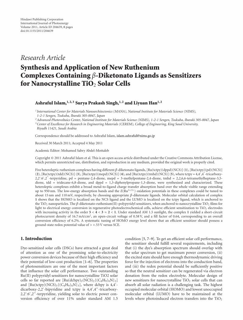
Hindawi Publishing CorporationInternational Journal of PhotoenergyVolume 2011, Article ID 204639, 8 pagesdoi:10.1155/2011/204639
Research Article
Synthesis and Application of New RutheniumComplexes Containing β-Diketonato Ligands as Sensitizersfor Nanocrystalline TiO2 Solar Cells
Ashraful Islam,1, 2, 3 Surya Prakash Singh,1, 2 and Liyuan Han1, 2
1 International Center for Materials Nanoarchitectonics (MANA), National Institute for Materials Science (NIMS),1-2-1 Sengen, Tsukuba, Ibaraki 305-0047, Japan
2 Advanced Photovoltaics Center, National Institute for Materials Science (NIMS), 1-2-1 Sengen, Tsukuba, Ibaraki 305-0047, Japan3 Center of Excellence for Research in Engineering Materials (CEREM), College of Engineering, King Saud University,Riyadh 11421, Saudi Arabia
Correspondence should be addressed to Ashraful Islam, [email protected]
Received 30 March 2011; Accepted 4 May 2011
Academic Editor: Mohamed Sabry Abdel-Mottaleb
Copyright © 2011 Ashraful Islam et al. This is an open access article distributed under the Creative Commons Attribution License,which permits unrestricted use, distribution, and reproduction in any medium, provided the original work is properly cited.
Five heteroleptic ruthenium complexes having different β-diketonato ligands, [Ru(tctpy)(dppd)(NCS)] (1), [Ru(tctpy)(pd)(NCS)](2), [Ru(tctpy)(tdd)(NCS)] (3), [Ru(tctpy)(mepd)(NCS)] (4), and [Ru(tctpy)(tmhd)(NCS)] (5), where tctpy = 4,4′,4”-tricarboxy-2,2′:6′,2′′ -terpyridine, pd = pentane-2,4-dione, mepd = 3-methylpentane-2,4-dione, tmhd = 2,2,6,6-tetramethylheptane-3,5-dione, tdd = tridecane-6,8-dione, and dppd = 1,3-diphenylpropane-1,3-dione, were synthesized and characterized. Theseheteroleptic complexes exhibit a broad metal-to-ligand charge transfer absorption band over the whole visible range extendingup to 950 nm. The low-energy absorption bands and the E(Ru3+/2+) oxidation potentials in these complexes could be tuned toabout 15 nm and 110 mV, respectively, by choosing appropriate β-diketonate ligands. Molecular orbital calculation of complex1 shows that the HOMO is localized on the NCS ligand and the LUMO is localized on the tctpy ligand, which is anchored tothe TiO2 nanoparticles. The β-diketonato-ruthenium(II)-polypyridyl sensitizers, when anchored to nanocrystalline TiO2 films forlight to electrical energy conversion in regenerative photoelectrochemical cells, achieve efficient sensitization to TiO2 electrodeswith increasing activity in the order 5 < 4 < 3 ≈ 2 < 1. Under standard AM 1.5 sunlight, the complex 1 yielded a short-circuitphotocurrent density of 16.7 mA/cm2, an open-circuit voltage of 0.58 V, and a fill factor of 0.64, corresponding to an overallconversion efficiency of 6.2%. A systematic tuning of HOMO energy level shows that an efficient sensitizer should possess aground-state redox potential value of > +.53 V versus SCE.
1. Introduction
Dye-sensitized solar cells (DSCs) have attracted a great dealof attention as one of the promising solar-to-electricitypower conversion devices because of their high efficiency andtheir potential of low-cost production [1–6]. The propertiesof photosensitizers are one of the most important factorsthat influence the solar cell performance. Two outstandingRu(II) polypyridyl sensitizers for nanocrystalline TiO2 solarcells so far reported are [Ru(dcbpy)2(NCS)2{(C4H9)4N}2]and [Ru(tctpy)(NCS)3{(C4H9)4N}3], where dcbpy is 4,4′-dicarboxy-2,2′-bipyridine and tctpy is 4,4′,4′′-tricarboxy-2,2′:6′,2′′-terpyridine, yielding solar to electric power con-version efficiency of over 11% under standard AM 1.5
condition [5, 7–9]. To get an efficient solar cell performance,the sensitizer should fulfill several requirements, includingthat (i) the dye’s absorption spectrum should overlap withthe solar spectrum to get maximum power conversion, (ii)the excited state should have enough thermodynamic drivingforce for the injection of electrons into the conduction band,and (iii) the redox potential should be sufficiently positiveso that the neutral sensitizer can be regenerated via electrondonation from the redox electrolyte. Molecular design ofnew sensitizers for nanocrystalline TiO2 solar cells that canabsorb all solar radiation is a challenging task. The highestoccupied molecular orbital (HOMO) and lowest unoccupiedmolecular orbital (LUMO) have to be maintained at thelevels where photoinduced electron transfers into the TiO2
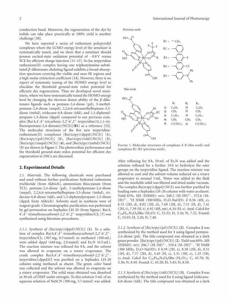
2 International Journal of Photoenergy
conduction band. Moreover, the regeneration of the dye byiodide can take place practically at 100% yield is anotherchallenge [10].
We have reported a series of ruthenium polypyridylcomplexes where the LUMO energy level of the sensitizer issystematically tuned, and we show that a sensitizer shouldpossess excited-state oxidation potential of −0.8 V versusSCE for efficient charge injection [11–17]. So far, terpyridineruthenium(II) complex having one triphenylamine-substi-tuted β-diketonato chelating ligand exhibits a broad absorp-tion spectrum covering the visible and near-IR regions anda high molar extinction coefficient [14]. However, there is noreport of systematic tuning of the HOMO energy level toelucidate the threshold ground-state redox potential forefficient dye regeneration. Thus we developed novel sensi-tizers, where we have systematically tuned the HOMO energylevel by changing the electron donor ability of the β-dike-tonato ligands such as pentane-2,4-dione (pd), 3-methyl-pentane-2,4-dione (mepd), 2,2,6,6-tetramethylheptane-3,5-dione (tmhd), tridecane-6,8-dione (tdd), and 1,3-diphenyl-propane-1,3-dione (dppd) compared to our previous com-plex [Ru(4,4′,4′′-tricarboxy-2,2′:6′,2′′-terpyridine)(1,1,1-tri-fluoropentane-2,4-dionato)(NCS)](R1) as a reference [13].The molecular structures of the five new terpyridine-ruthenium(II) complexes [Ru(tctpy)(dppd)(NCS)] (1),[Ru(tctpy)(pd)(NCS)] (2), [Ru(tctpy)(tdd)(NCS)] (3),[Ru(tctpy)(mepd)(NCS)] (4), and [Ru(tctpy)(tmhd)(NCS)](5) are shown in Figure 1. The photovoltaic performance andthe threshold ground-state redox potential for efficient dyeregeneration in DSCs are discussed.
2. Experimental Details
2.1. Materials. The following chemicals were purchasedand used without further purification: hydrated rutheniumtrichloride (from Aldrich), ammonium thiocyanate (fromTCI), pentane-2,4-dione (pd), 3-methylpentane-2,4-dione(mepd), 2,2,6,6-tetramethylheptane-3,5-dione (tmhd), tri-decane-6,8-dione (tdd), and 1,3-diphenylpropane-1,3-dione(dppd; from Aldrich). Solvents used in synthesis were ofreagent grade. Chromatographic purification was performedby gel permeation on Sephadex LH-20 (from Sigma). Ru(4,4′,4′′-trimethoxycarbonyl-2,2′:6′,2′′-terpyridine)Cl3 [7] wassynthesized using literature procedures.
2.1.1. Synthesis of [Ru(tctpy)(dppd)(NCS)] (1). To a solu-tion of complex Ru(4,4′,4′′-trimethoxycarbonyl-2,2′:6′,2′′-terpyridine)Cl3 (307 mg, 0.5 mmol) in methanol (100 mL)were added dppd (448 mg, 2.0 mmol) and Et3N (0.5 mL).The reaction mixture was refluxed for 8 h, and the solventwas allowed to evaporate on a rotary evaporator. Thecrude complex Ru(4,4′,4′′-trimethoxycarbonyl-2,2′:6′,2′′-terpyridine)(dppd)Cl was purified on a Sephadex LH-20column using methanol as eluent. The green color bandwas collected and the solvent was allowed to evaporate ona rotary evaporator. The solid mass obtained was dissolvedin 30 mL of DMF under nitrogen. To this solution 5 mL of anaqueous solution of NaSCN (300 mg, 3.7 mmol) was added.
HO
HO
HO
HO
O
O O
O
O
O
O
O
O
O
N
N
N
N
N
N
N
N
NC
C
S
S
OH
OH
Ru
Ru
R
F
F
FF
R1
R1
R2
R2
R3
R3
R4
R5
CH3
CH3 CH3
CH3CH3CH3
CI
Ph
Ph
Previous work
This work
1:2:3:4:5:
R1 R2 R3
C6H5 C6H5HH
H
H
C5H11 C5H11
C(CH3)3 C(CH3)3
=
=
=
=
=
Figure 1: Molecular structures of complexes 1–5 (this work) andcomplexes R1–R5 (previous work).
After refluxing for 8 h, 10 mL of Et3N was added and thesolution refluxed for a further 24 h to hydrolyze the estergroups on the terpyridine ligand. The reaction mixture wasallowed to cool and the solvent volume reduced on a rotaryevaporator to around 5 mL. Water was added to the flaskand the insoluble solid was filtered and dried under vacuum.The complex Ru(tctpy)(dppd)(NCS) was further purified byloading onto a Sephadex LH-20 column with water as eluent.Yield 65%. MS (ESIMS): m/z: 248.2 (M-3H)3−, 372.6 (M-2H)2−. 1H NMR (300 MHz, D2O-NaOD): δ 8.56 (4H, s),8.53 (2H, d), 8.02 (2H, d), 7.69 (2H, d), 7.51 (H, d), 7.41(2H, t), 7.39 (H, t), 6.92 (4H, sm), 6.34 (H, s). Anal. Calcd forC34H22N4O8SRu·(H2O): C, 53.33; H, 3.16; N, 7.32. Found:C, 53.03; H, 3.20; N, 7.40.
2.1.2. Synthesis of [Ru(tctpy)(pd)(NCS)] (2). Complex 2 wassynthesized by the method used for 1 using ligand pentane-2,4-dione (pd). The title compound was obtained as a darkgreen powder. [Ru(tctpy)(pd)(NCS)] (2). Yield was 60%. MS(ESIMS): m/z: 206.7 (M-3H)3−, 310.4 (M-2H)2−. 1H NMR(300 MHz, D2O-NaOD): δ 8.59 (2H, s), 8.58 (2H, d), 8.51(2H, d), 7.77 (2H, d), 5.45 (H, s), 2.31 (3H, s), 1.25 (3H,s)..Anal. Calcd for C24H18N4O8SRu·(H2O)2: C, 43.70; H,3.36; N, 8.49. Found: C, 43.20; H, 3.45; N, 8.50.
2.1.3. Synthesis of [Ru(tctpy)(tdd)(NCS)] (3). Complex 3 wassynthesized by the method used for 1 using ligand tridecane-6,8-dione (tdd). The title compound was obtained as a dark

International Journal of Photoenergy 3
green powder. [Ru(tctpy)(tdd)(NCS){(C4H9)4N}] (3). Yieldwas 56%. MS (ESIMS): m/z: 244.1 (M-3H)3−, 367.4 (M-2H)2−. 1H NMR (300 MHz, D2O-NaOD): δ 8.41 (4H, s),8.31 (2H, d), 7.63 (2H, d), 5.21 (H, s), 2.33 (2H, t), 1.60(2H, m), 1.29 (2H, t), 1.18 (4H, m), 0.65 (2H, t), 0.51 (3H,m), 0.38 (2H, m), 0.13 (2H, t), 0.02 (3H, m). Anal. Calcd forC32H35N4O8SRu: C, 52.17; H, 4.79; N, 7.60. Found: C, 51.85;H, 4.81; N, 7.85.
2.1.4. Synthesis of [Ru(tctpy)(mepd)(NCS)] (4). Complex 4was synthesized by the method used for 1 using ligand 3-methylpentane-2,4-dione (mepd). The title compound wasobtained as a dark green powder. [Ru(tctpy)(mepd)(NCS)](4). Yield was 35%. MS (ESIMS): m/z: 211.8 (M-3H)3−,313.3 (M-2H)2−.1H NMR (300 MHz, D2O-NaOD): δ 8.60(2H, s), 8.58 (2H, d,), 7.78 (2H, d), 2.45 (3H, s), 1.78 (3H, s),1.32 (3H, s). Anal. Calcd for C25H20N4O8SRu: C, 47.09; H,3.16; N, 8.79. Found: C, 46.74; H, 3.23; N, 8.86.
2.1.5. Synthesis of [Ru(tctpy)(tmhd)(NCS)] (5). Complex5 was synthesized by the method used for 1 usingligand 2,2,6,6-tetramethylheptane-3,5-dione (tmhd). Thetitle compound was obtained as a dark green powder.[Ru(tctpy)(tmhd)(NCS)] (5). Yield was 55%. MS (ESIMS):m/z: 234.6 (M-3H)3−, 352.7 (M-2H)2−, 707.0 (M-H)−.1HNMR (300 MHz, D2O-NaOD): δ 8.26 (4H, s), 8.13 (2H, d),7.44 (2H, d), 5.40 (H, s), 1.03 (9H, s), 0.00 (9H, s). Anal.Calcd for C30H31N4O8SRu · (H2O): C, 49.65; H, 4.44; N,7.72. Found: C, 49.77 H, 4.62N, 7.89.
2.2. Spectroscopic Measurements. UV-visible spectra wererecorded on a Shimadzu UV-3101PC spectrophotometer.Steady-state emission spectra were recorded using a gratingmonochromator (Triax 1900) and a CCD image sensor. Thespectral sensitivity of the spectrophotometer was calibratedusing a bromine lamp (Ushio IPD100 V 500 WCS). Theemission lifetimes were measured by exciting the sample witha∼7 ns pulse at 500 nm from an optical parametric oscillator(Surelite OPO) pumped at 355 nm by a Nd : YAG laser(Continum Surelite II). The emission decay was followedon a Tektronix TDS680C digitizing signal analyzer, havingused a Hamamatsu R928 photomultiplier to convert the lightsignal to a voltage signal. Dewar vessel was used for themeasurements at 77 K. 1H NMR spectra were recorded bya Varian 300 BB spectrometer. Electrospray ionization massspectra (ESIMS) were obtained on a Micromass Quattro IImass spectrometer.
2.3. Electrochemical Measurements. The redox potential ofthe complexes was measured using a standard three-electrode apparatus. The counter electrode was a platinumwire, the working electrode was a ruthenium-complex-adsorbed conducting nanocrystalline TiO2 film, and thereference electrode was an Ag/AgCl (saturated aqueous KCl)in contact with a KCl salt bridge. Cyclic voltammogramswere collected using an electrochemical analyzer. Scan rateswere 0.05–0.5 Vs−1. Acetonitrile was used as solvent andthe supporting electrolyte was 0.1 M tetrabutylammonium
perchlorate. Electrode potential values were calibrated to thesaturated calomel electrode (SCE).
2.4. Preparation of TiO2 Electrode. Nanocrystalline TiO2
photoelectrodes of around 20 μm thickness (area: 0.25 cm2)were prepared using a variation of a method reported byNazeeruddin et al. [7]. Fluorine-doped tin oxide-coated glasselectrodes (Nippon Sheet Glass Co., Japan) with a sheetresistance of 8–10 ohm−2 and an optical transmission of>80% in the visible range were used. Anatase TiO2 colloids(particle size ∼13 nm) were obtained from commercialsources (Ti-Nanoxide D/SP, Solaronix). The nanocrystallineTiO2 thin films of approximately 20 μm thickness weredeposited onto the conducting glass by screen-printing. Thefilm was then sintered at 500◦C for 1 h. The film thicknesswas measured with a Surfcom 1400 A surface profiler (TokyoSeimitsu Co. Ltd.). The electrodes were impregnated witha 50 mM titanium tetrachloride solution and sintered at500◦C. The dye solutions (2 × 10⁻⁴ M) were prepared in1 : 1 acetonitrile and tert-butyl alcohol solvents. Deoxycholicacid as a coadsorbent was added to the dye solution at aconcentration of 20 mM. The electrodes were immersed inthe dye solutions and then kept at 25◦C for 20 h to adsorbthe dye onto the TiO2 surface.
2.5. Fabrication of Dye-Sensitized Solar Cell. Photovoltaicmeasurements were performed in a two-electrode sandwichcell configuration. The dye-deposited TiO2 film was used asthe working electrode, and a platinum-coated conductingglass was used as the counter electrode. Two electrodes wereseparated by a surlyn spacer (40 μm thick) and sealed up byheating the polymer frame. The electrolyte was composed of0.6 M dimethylpropyl-imidazolium iodide (DMPII), 0.05 MI2, and 0.1 M LiI in acetonitrile (AN).
2.6. Photovoltaic Characterization. The working electrodewas illuminated through a conducting glass. The current-voltage characteristics were measured by using the previouslyreported method [18] with a solar simulator (AM-1.5,100 mW/cm2, WXS-155S-10: Wacom Denso Co. Japan).Monochromatic incident photon-to-current conversion effi-ciency (IPCE) for the solar cell, plotted as a functionof excitation wavelength, was recorded on a CEP-2000system (Bunkoh-Keiki Co. Ltd.). Incident photon-to-currentconversion efficiency (IPCE) at each incident wavelength wascalculated from (1), where Isc is the photocurrent density atshort circuit in mA cm−2 under monochromatic irradiation,q is the elementary charge, λ is the wavelength of incidentradiation in nm, and P0 is the incident radiative flux in Wm−2
IPCE(λ) = 1240
(Isc
qλP0
). (1)
3. Results and Discussion
3.1. Photophysical Properties. The absorption, emission, andelectrochemical properties of complexes 1–5 and reference
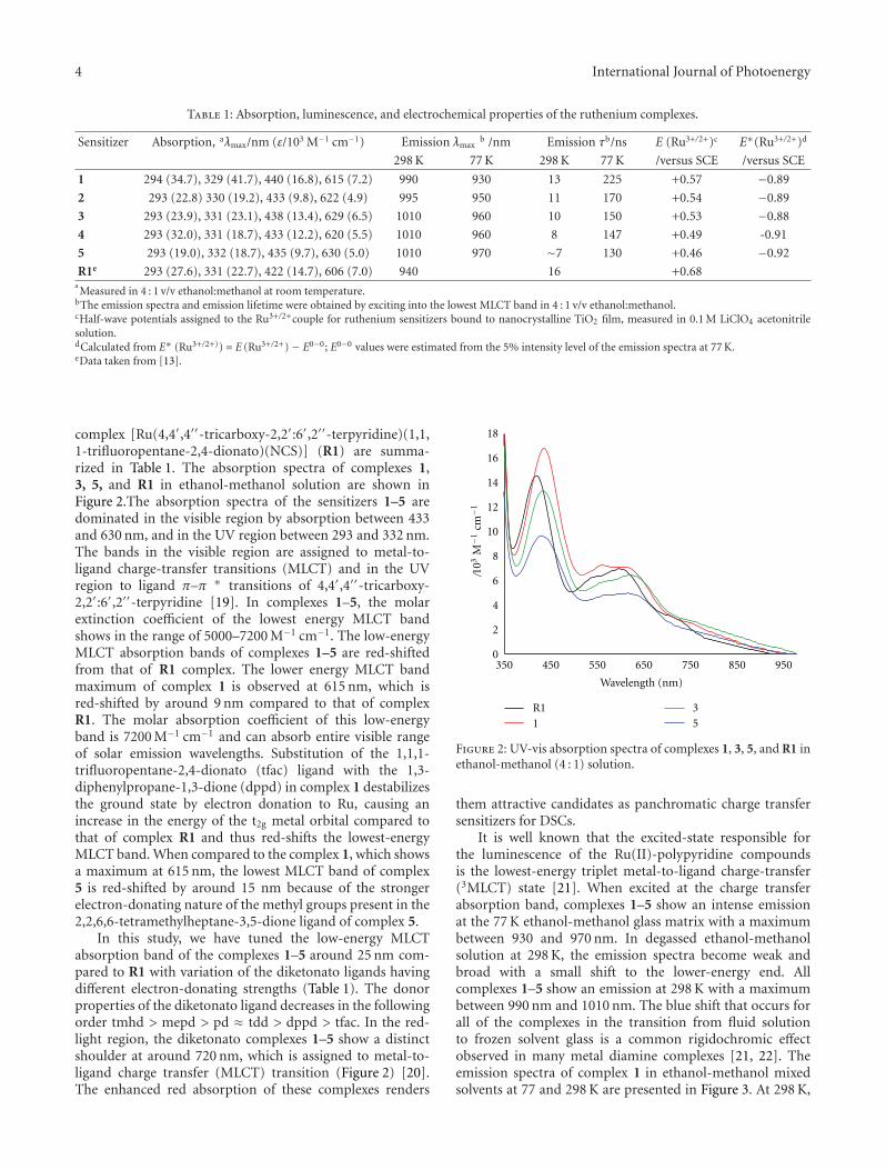
4 International Journal of Photoenergy
Table 1: Absorption, luminescence, and electrochemical properties of the ruthenium complexes.
Sensitizer Absorption, aλmax/nm (ε/103 M−1 cm−1) Emission λmaxb /nm Emission τb/ns E (Ru3+/2+)c E∗(Ru3+/2+)d
298 K 77 K 298 K 77 K /versus SCE /versus SCE
1 294 (34.7), 329 (41.7), 440 (16.8), 615 (7.2) 990 930 13 225 +0.57 −0.89
2 293 (22.8) 330 (19.2), 433 (9.8), 622 (4.9) 995 950 11 170 +0.54 −0.89
3 293 (23.9), 331 (23.1), 438 (13.4), 629 (6.5) 1010 960 10 150 +0.53 −0.88
4 293 (32.0), 331 (18.7), 433 (12.2), 620 (5.5) 1010 960 8 147 +0.49 -0.91
5 293 (19.0), 332 (18.7), 435 (9.7), 630 (5.0) 1010 970 ∼7 130 +0.46 −0.92
R1e 293 (27.6), 331 (22.7), 422 (14.7), 606 (7.0) 940 16 +0.68aMeasured in 4 : 1 v/v ethanol:methanol at room temperature.
bThe emission spectra and emission lifetime were obtained by exciting into the lowest MLCT band in 4 : 1 v/v ethanol:methanol.cHalf-wave potentials assigned to the Ru3+/2+couple for ruthenium sensitizers bound to nanocrystalline TiO2 film, measured in 0.1 M LiClO4 acetonitrilesolution.dCalculated from E∗ (Ru3+/2+)) = E (Ru3+/2+) − E0−0; E0−0 values were estimated from the 5% intensity level of the emission spectra at 77 K.eData taken from [13].
complex [Ru(4,4′,4′′-tricarboxy-2,2′:6′,2′′-terpyridine)(1,1,1-trifluoropentane-2,4-dionato)(NCS)] (R1) are summa-rized in Table 1. The absorption spectra of complexes 1,3, 5, and R1 in ethanol-methanol solution are shown inFigure 2.The absorption spectra of the sensitizers 1–5 aredominated in the visible region by absorption between 433and 630 nm, and in the UV region between 293 and 332 nm.The bands in the visible region are assigned to metal-to-ligand charge-transfer transitions (MLCT) and in the UVregion to ligand π–π ∗ transitions of 4,4′,4′′-tricarboxy-2,2′:6′,2′′-terpyridine [19]. In complexes 1–5, the molarextinction coefficient of the lowest energy MLCT bandshows in the range of 5000–7200 M−1 cm−1. The low-energyMLCT absorption bands of complexes 1–5 are red-shiftedfrom that of R1 complex. The lower energy MLCT bandmaximum of complex 1 is observed at 615 nm, which isred-shifted by around 9 nm compared to that of complexR1. The molar absorption coefficient of this low-energyband is 7200 M−1 cm−1 and can absorb entire visible rangeof solar emission wavelengths. Substitution of the 1,1,1-trifluoropentane-2,4-dionato (tfac) ligand with the 1,3-diphenylpropane-1,3-dione (dppd) in complex 1 destabilizesthe ground state by electron donation to Ru, causing anincrease in the energy of the t2g metal orbital compared tothat of complex R1 and thus red-shifts the lowest-energyMLCT band. When compared to the complex 1, which showsa maximum at 615 nm, the lowest MLCT band of complex5 is red-shifted by around 15 nm because of the strongerelectron-donating nature of the methyl groups present in the2,2,6,6-tetramethylheptane-3,5-dione ligand of complex 5.
In this study, we have tuned the low-energy MLCTabsorption band of the complexes 1–5 around 25 nm com-pared to R1 with variation of the diketonato ligands havingdifferent electron-donating strengths (Table 1). The donorproperties of the diketonato ligand decreases in the followingorder tmhd > mepd > pd ≈ tdd > dppd > tfac. In the red-light region, the diketonato complexes 1–5 show a distinctshoulder at around 720 nm, which is assigned to metal-to-ligand charge transfer (MLCT) transition (Figure 2) [20].The enhanced red absorption of these complexes renders
0
2
4
6
8
10
12
14
16
18
350 450 550 650 750 850 950
/103
M−1
cm−1
Wavelength (nm)
R11
35
Figure 2: UV-vis absorption spectra of complexes 1, 3, 5, and R1 inethanol-methanol (4 : 1) solution.
them attractive candidates as panchromatic charge transfersensitizers for DSCs.
It is well known that the excited-state responsible forthe luminescence of the Ru(II)-polypyridine compoundsis the lowest-energy triplet metal-to-ligand charge-transfer(3MLCT) state [21]. When excited at the charge transferabsorption band, complexes 1–5 show an intense emissionat the 77 K ethanol-methanol glass matrix with a maximumbetween 930 and 970 nm. In degassed ethanol-methanolsolution at 298 K, the emission spectra become weak andbroad with a small shift to the lower-energy end. Allcomplexes 1–5 show an emission at 298 K with a maximumbetween 990 nm and 1010 nm. The blue shift that occurs forall of the complexes in the transition from fluid solutionto frozen solvent glass is a common rigidochromic effectobserved in many metal diamine complexes [21, 22]. Theemission spectra of complex 1 in ethanol-methanol mixedsolvents at 77 and 298 K are presented in Figure 3. At 298 K,

International Journal of Photoenergy 5
0
5
10
750 850 950 1050 1150 1250
Em
issi
onin
ten
sity
(a.u
.)
Wavelength (nm)298 K
77 K
Figure 3: Emission spectra of complex 1 in ethanol-methanol (4 : 1)solution at 77 K (a) and 298 K (b).
complex 1 exhibits an emission maximum at 990 nm, whichis 50 nm red-shifted compared to that of the R1 emissionand consistent with the shift in the lowest-MLCT absorptionband. The luminescence data are gathered in Table 1. At77 K, complexes 1–5 displayed excited-state lifetimes rangingfrom 225 to 130 ns. The lifetimes decrease significantly withthe increase in temperature, to 7–13 ns in fluid solution at298 K. The very short-lived excited state in fluid solutionmay be caused by efficient nonradiative decay via low-lyingligand-field excited states [21]. The excited-state lifetime ofall the complexes is long enough for the process of electroninjection into the conduction band of the TiO2 electrodeto make it efficient enough [23, 24]. To become a suitablesensitizer in DSCs, the band structure of the metal complexshould match the conduction band of the semiconductorelectrode and the redox potential of the electrolyte. Theelectrochemical data of the complexes measured in methanolsolution are summarized in Table 1. All the complexes exhibitquasireversible oxidation wave for the Ru3+/2+ couple rangingfrom +0.46 to +0.57 V versus SCE. The formation of anMLCT excited state of these complexes formally involves theoxidation of a HOMO having metal t2g orbital characterand reduction of a diimine-based LUMO. Table 1 showsthat the ground-state oxidation potentials (Ru3+/2+) of theβ-diketonato complexes 1–5 are more negative than thoseof the complex R1. In these complexes, the energy of theacceptor orbital (LUMO) remains nearly constant and thedecrease in MLCT transition energy arises mainly from theincrease in the energy of the metal t2g orbital (HOMO).
The excited-state oxidation potential, E∗ (Ru3+/2+), is ameasure of the loss of the electron that is placed in theπ ∗ (terpyridine) LUMO upon excitation. For complexes1–5, E∗ (Ru3+/2+) values are estimated using equation (2),where E (Ru3+/2+) is the oxidation potential of the groundstate and E0−0 is the energy difference between the lowest
HOMO
(a)
LUMO
(b)
Figure 4: Graphic representation of the frontier molecular orbitalsof complex 1.
excited and ground states. The resulting E∗ (Ru3+/2+) valuesare shown in Table 1. The excited states of complexes 1–5lie above the conduction band edge (–0.82 V versus SCE)of the nanocrystalline TiO2 [2]. Efficient electron injectioninto the conduction band of the TiO2 is thus possible forall of complexes 1–5. The oxidation potential values of thecomplexes 1–5 lie above the I−3 /I− redox couple (0.07 V versusSCE) [25]
E∗(
Ru3+/2+)= E∗
(Ru3+/2+
)− E0−0. (2)
To get an insight into the electron distribution of this newseries of complexes for better understanding of the chargeinjection and dye regeneration process, the highest occupiedmolecular orbital (HOMO) and the lowest unoccupiedmolecular orbital (LUMO) of complex 1 were calculatedby using Gaussian-03 program package (Figure 4). TheHOMO of complex 1 is delocalized on Ru metal andNCS ligand, and the amplitude is primarily delocalized onthe sulfur atom within the NCS ligand. The NCS grouppointing in the direction of the electrolyte may facilitatereduction of the oxidized dye (Ru3+) through reaction with

6 International Journal of Photoenergy
0
20
40
60
80
400 500 600 700 800 900
IPC
E(%
)
Wavelength (nm)
124
Figure 5: Photocurrent action spectra obtained with complexes 1(a), 2 (b), and 4 (c) attached to nanocrystalline TiO2 film. Theincident photon-to-current conversion efficiency is plotted as afunction of wavelength. A sandwich type sealed cell configurationwas used to measure this spectrum. The electrolyte composition was0.6 M DMPII, 0.05 M I2, and 0.1 M LiI in acetonitrile.
I−. The β-diketonato ligand has a negligible contribution toHOMO. The LUMO has homogeneous amplitudes on theterpyridine ligand, facilitating the electron injection from thephotoexcited sensitizer to the TiO2 semiconductor.
3.2. Photovoltaic Properties. The photovoltaic performanceof complexes 1–5 on nanocrystalline TiO2 electrode wasstudied under standard AM 1.5 irradiation (100 mW cm−2)using an electrolyte with a composition of 0.6 Mdimethylpropyl-imidazolium iodide (DMPII), 0.05 M I2, and0.1 M LiI in acetonitrile. Figure 5 shows the photocurrentaction spectra for complexes 1, 2, and 4 where the incidentphoton to current conversion efficiency (IPCE) values isplotted as a function of wavelength. The maximum IPCEvalues of complexes 1–5 are listed in Table 2. Complexes 1–3achieved efficient sensitization of nanocrystalline TiO2 overthe whole visible range extending into the near IR region.The most efficient sensitizer in this series was complex 1that shows an IPCE value of 70% in the plateau region.Taking into account the reflection and absorption lossesby the conducting glass, the photon-to-current conversionefficiency in this range reaches around 85%. One of thepossible explanations for this low IPCE value of complex 1is the aggregation of sensitizer molecules on TiO2 surface.The red response was improved by replacing dppd with tddwhile injection efficiencies were very low throughout thevisible region (Figure 5). The maximum IPCE values of theseβ-diketonato complexes 1–5 decreases with the decreasein the ground-state oxidation potentials (Ru3+/2+) values.Complexes 4 and 5 showed a drastically reduced IPCE value
Table 2: Photovoltaic properties of ruthenium polypyridyl sensiti-zersa.
Sensitizer IPCEmax Jsc (mA cm−2) Voc (V) FF η (%)
1 70 16.7 0.58 0.64 6.2
2 61 14.2 0.57 0.66 5.3
3 54 13.0 0.58 0.70 5.3
4 30 7.6 0.56 0.70 3.0
5 24 6.2 0.45 0.71 2.0
R1b 70 18.3 0.57 0.64 6.7aConditions: sealed cells; coadsorbate, DCA 40 mM; photoelectrode, TiO2
(20 μm thickness and 0.25 cm2); electrolyte, 0.6 M DMPII, 0.1 M LiI, 0.05 I2
in AN; irradiated light, AM 1.5 solar light (100 mW cm−2). Jsc, short-circuitphotocurrent density; Voc, open-circuit photovoltage; FF, fill factor; η, totalpower conversion efficiency; IPCE, incident photon-to-current conversionefficiency.bData taken from [13].
(i.e., <30%) in the plateau region, and this reduction maybe due to the decrease in the dye regeneration rate aftertuning the ground-state oxidation potential toward morenegative range. The recombination rate of injected electronswith the oxidized dye is an important factor that affectsthe electron collection efficiency. The recombination rateswill increase by changing the oxidation values toward morenegative potential. After electron injection, a competition issetup between charge recombination and iodide oxidationby oxidized dye. Considering the relative driving forceof these complexes, the charge recombination rates willincrease in the order of 1 < 2 ≈ 3 <4 ≈ 5. The low injectionefficiencies (IPCEmax = 24–30%) of the complexes 4-5compared to the complexes 1–3 can be explained by the factthat these complexes have more negative Ru3+/2+ groundstate oxidation potential compared to those of the complexes1–3 and the back reaction of injected electrons with Ru(III)competes to regeneration of Ru(II) through reaction withiodide. The ground-state potential of complex 3 (+0.53 Vversus SCE) offers a minimum limit for the ground-stateredox potential of the dye in the current configuration of theelectrochemical cell and redox couple.
Figure 6 shows the photocurrent-voltage curves obtainedunder AM1.5 simulated illumination of the various dyecoated TiO2 electrode systems studied in this work. Theshort-circuit photocurrent density (Jsc), open-circuit voltage(Voc), fill factors (FF), and overall cell efficiencies (η)for each dye-TiO2 electrode are summarized in Table 2.The dppd complex 1 shows the best performance in thisseries. The solar cell sensitized with complex 1 showeda photocurrent density of 16.7 mA cm−2, an open circuitpotential of 0.58 V, and a fill factor of 0.64, corresponding toan overall conversion efficiency (η) of 6.2%. The complexes4-5 showed poor cell performance (η < 3%) compare to thoseof complexes 1–3. The low injection efficiencies (IPCEmax
= 24–30%) of complexes 4-5 decrease the short-circuitphotocurrent density (Jsc), and thus the decrease of overallcell efficiencies.
Thus, this class of diketonato ruthenium complexesserves as a basis for further design of new potential sensitizersby introducing suitable substituents on the diketonato ligand

International Journal of Photoenergy 7
0
5
10
15
20
0 0.1 0.2 0.3 0.4 0.5 0.6
Ph
otoc
urr
ent
den
sity
(mA
cm−2
)
Voltage (V)
12
Figure 6: Photocurrent voltage characteristics of DSCs sensitizedwith the complexes 1 (a) and 2 (b) at AM 1.5 illuminations (lightintensities: 100 mW cm−2. The redox electrolyte consisted of asolution of 0.6 M DMPII, 0.05 M I2, and 0.1 M LiI in acetonitrile.
to adjust a desired electronic environment on the metalcenter for efficient dye regeneration. Since the modificationsof electronic and steric environments in the sensitizingmolecules are possible by changing the substituents on thediketonate ligand, further improvement in the solar cellefficiency will be accomplished in the near future.
4. Conclusions
Five new panchromatic photosensitizers based on 4,4′,4′′-tricarboxy-2,2′:6′,2′′-terpyridine -ruthenium(II) complexeswith one β-diketonato chelating ligand, pentane-2,4-dione (pd), 3-methylpentane-2,4-dione (mepd), 2,2,6,6-tetramethylheptane-3,5-dione (tmhd), tridecane-6,8-dione(tdd), or 1,3-diphenylpropane-1,3-dione (dppd) were devel-oped, and systematically characterized using electrochemicaland spectroscopic methods. The low-energy MLCT tran-sitions in these complexes have been tuned by increasingthe donor strength of the β-diketonato ligand to extendthe spectral response of nanocrystalline TiO2 electrodesto a range of longer wavelengths. The decrease in MLCTtransition energy arises mainly from the negative shift inthe ground state oxidation potential, that is, the energyof the metal t2g orbital (HOMO).The complexes achievedefficient sensitization of nanocrystalline TiO2 over the wholevisible range extending into the near IR region (ca. 950 nm).The photovoltaic data of these new complexes shows 6.2%power conversion efficiency under standard AM 1.5 irra-diation (100 mW cm−2). Though complexes 4 and 5 havesuperior panchromatic light-harvesting properties comparedto the complex 1, they show poor overall photovoltaicperformance. A sluggish halide oxidation rate and a fastrecombination of injected electron with the oxidized dye dueto unfavorable HOMO energy level are perhaps responsiblefor the low cell efficiency of these complexes.
References
[1] B. O’Regan and M. Gratzel, “A low-cost, high-efficiency solarcell based on dye-sensitized colloidal TiO2 films,” Nature, vol.353, no. 6346, pp. 737–740, 1991.
[2] A. Hagfeld and M. Gratzel, “Light-induced redox reactions innanocrystalline systems,” Chemical Reviews, vol. 95, no. 1, pp.49–68, 1995.
[3] M. Gratzel, “Conversion of sunlight to electric power bynanocrystalline dye-sensitized solar cells,” Journal of Photo-chemistry and Photobiology A, vol. 164, no. 1–3, pp. 3–14, 2004.
[4] A. Hagfeldt and M. Gratzel, “Molecular photovoltaics,”Accounts of Chemical Research, vol. 33, no. 5, pp. 269–277,2000.
[5] M. K. Nazeeruddin, A. Kay, I. Rodicio et al., “Conversionof light to electricity by cis-X2bis(2,2′-bipyridyl-4,4′-dicar-boxylate)ruthenium(II) charge-transfer sensitizers (X = Cl−,Br−, I−, CN−, and SCN−) on nanocrystalline TiO2 electrodes,”Journal of the American Chemical Society, vol. 115, no. 14, pp.6382–6390, 1993.
[6] K. Hara, H. Sugihara, Y. Tachibana et al., “Dye-sensitizednanocrystalline TiO2 solar cells based on ruthenium(II)phenanthroline complex photosensitizers,” Langmuir, vol. 17,no. 19, pp. 5992–5999, 2001.
[7] M. K. Nazeeruddin, P. Pechy, T. Renouard et al., “Engineeringof efficient panchromatic sensitizers for nanocrystalline TiO2-based solar cells,” Journal of the American Chemical Society, vol.123, no. 8, pp. 1613–1624, 2001.
[8] M. K. Nazeeruddin, F. D. Angelis, S. Fantacci et al., “Combinedexperimental and DFT-TDDFT computational study of pho-toelectrochemical cell ruthenium sensitizers,” Journal of theAmerican Chemical Society, vol. 127, no. 48, pp. 16835–16847,2005.
[9] Y. Chiba, A. Islam, Y. Watanabe, R. Komiya, N. Koide, and L.Han, “Dye-sensitized solar cells with conversion efficiency of11.1%,” Japanese Journal of Applied Physics, vol. 45, no. 25, pp.L638–L640, 2006.
[10] A. Islam, H. Sugihara, and H. Arakawa, “Molecular designof ruthenium(II) polypyridyl photosensitizers for efficientnanocrystalline TiO2 solar cells,” Journal of Photochemistry andPhotobiology A, vol. 158, no. 2–3, pp. 131–138, 2003.
[11] A. Islam, F. A. Chowdhury, Y. Chiba et al., “Synthesisand characterization of new efficient tricarboxyterpyridyl (β-diketonato) ruthenium(II) sensitizers and their applications indye-sensitized solar cells,” Chemistry of Materials, vol. 18, no.22, pp. 5178–5185, 2006.
[12] A. Islam, F. A. Chowdhury, Y. Chiba et al., “Ruthenium(II)tricarboxyterpyridyl complex with a fluorine-substituted β-diketonato ligand for highly efficient dye-sensitized solarcells,” Chemistry Letters, vol. 34, no. 3, pp. 344–345, 2005.
[13] A. Islam, H. Sugihara, M. Yanagida et al., “Efficient panchro-matic sensitization of nanocrystalline TiO2 films by β-diketonato ruthenium polypyridyl complexes,” New Journal ofChemistry, vol. 26, no. 8, pp. 966–968, 2002.
[14] S. Gao, A. Islam, Y. Numata, and L. Han, “A β-diketonatoruthenium(II) complex with high molar extinction coefficientfor panchromatic sensitization of nanocrystalline TiO2 film,”Applied Physics Express, vol. 3, no. 6, Article ID 062301, 3pages, 2010.
[15] S. P. Singh, A. Islam, M. Yanagida, and L. Han, “Developmentof a new class of thiocyanate-free cyclometallated ruthe-nium(II) complex for sensitizing nanocrystalline TiO2 solarcells,” International Journal of Photoenergy, vol. 2011, p. 5,2011.
8 International Journal of Photoenergy
[16] A. Islam, S. P. Singh, M. Yanagida, R. Karim, and L. Han,“Amphiphilic ruthenium(II) terpyridine sensitizers with longalkyl chain substituted β-diketonato ligands: An efficientcoadsorbent free dye-sensitized solar cells,” InternationalJournal of Photoenergy, vol. 2011, p. 7, 2011.
[17] A. Islam, S. P. Singh, and L. Han, “Thiocyanate-free,panchromatic ruthenium(II) terpyridine sensitizer having atridentate diethylenetriamine ligand for near-IR sensitizationof nanocrystalline TiO2,” Functional Materials Letters, vol. 4,no. 1, pp. 21–24, 2011.
[18] N. Koide and L. Han, “Measuring methods of cell performanceof dye-sensitized solar cells,” Review of Scientific Instruments,vol. 75, no. 9, pp. 2828–2831, 2004.
[19] A. Mamo, A. Juris, G. Calogero, and S. Campagna, “Near-infrared luminescence at room temperature of two newosmium(II) terdentate polypyridine complexes,” ChemicalCommunications, no. 10, pp. 1225–1226, 1996.
[20] Y. Takahashi, H. Arakawa, H. Sugihara et al., “Highly effi-cient polypyridyl-ruthenium(II) photosensitizers with chelat-ing oxygen donor ligands: β-diketonato-bis(dicarboxybi-pyri-dine)ruthenium,” Inorganica Chimica Acta, vol. 310, no. 2, pp.169–174, 2000.
[21] A. Islam, N. Ikeda, A. Yoshimura, and T. Ohno, “Nonra-diative transition of phosphorescent charge-transfer statesof ruthenium(II)-to-2, 2′-biquinoline and ruthenium(II)-to-2, 2′ :6′, 2
′′-terpyridine in the solid state,” Inorganic Chemi-
stry, vol. 37, no. 12, pp. 3093–3098, 1998.[22] A. Juris, V. Balzani, F. Barigelletti, S. Campagna, P. Belser, and
A. Zelewsky, “Ru(II) polypyridine complexes: photophysics,photochemistry, eletrochemistry, and chemiluminescence,”Coordination Chemistry Reviews, vol. 84, no. C, pp. 85–277,1988.
[23] Y. Tachibana, S. A. Haque, I. P. Mercer, J. R. Durrant, and D. R.Klug, “Electron injection and recombination in dye sensitizednanocrystalline titanium dioxide films: a comparison ofruthenium bipyridyl and porphyrin sensitizer dyes,” Journalof Physical Chemistry B, vol. 104, no. 6, pp. 1198–1205, 2000.
[24] J. M. Rehm, G. L. McLendon, Y. Nagasawa, K. Yoshihara, J.Moser, and M. Gratzel, “Femtosecond electron-transfer dyna-mics at a sensitizing dye-semiconductor (TiO2) interface,”Journal of Physical Chemistry, vol. 100, no. 23, pp. 9577–9578,1996.
[25] G. Oskam, B. V. Bergeron, G. J. Meyer, and P. C. Searson,“Pseudohalogens for dye-sensitized TiO2 photoelectrochem-ical cells,” Journal of Physical Chemistry B, vol. 105, no. 29, pp.6867–6873, 2001.
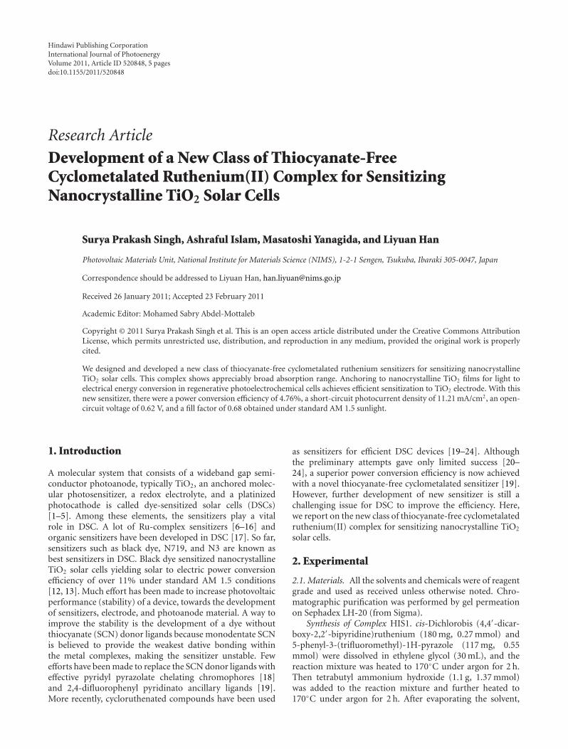
Hindawi Publishing CorporationInternational Journal of PhotoenergyVolume 2011, Article ID 520848, 5 pagesdoi:10.1155/2011/520848
Research Article
Development of a New Class of Thiocyanate-FreeCyclometalated Ruthenium(II) Complex for SensitizingNanocrystalline TiO2 Solar Cells
Surya Prakash Singh, Ashraful Islam, Masatoshi Yanagida, and Liyuan Han
Photovoltaic Materials Unit, National Institute for Materials Science (NIMS), 1-2-1 Sengen, Tsukuba, Ibaraki 305-0047, Japan
Correspondence should be addressed to Liyuan Han, [email protected]
Received 26 January 2011; Accepted 23 February 2011
Academic Editor: Mohamed Sabry Abdel-Mottaleb
Copyright © 2011 Surya Prakash Singh et al. This is an open access article distributed under the Creative Commons AttributionLicense, which permits unrestricted use, distribution, and reproduction in any medium, provided the original work is properlycited.
We designed and developed a new class of thiocyanate-free cyclometalated ruthenium sensitizers for sensitizing nanocrystallineTiO2 solar cells. This complex shows appreciably broad absorption range. Anchoring to nanocrystalline TiO2 films for light toelectrical energy conversion in regenerative photoelectrochemical cells achieves efficient sensitization to TiO2 electrode. With thisnew sensitizer, there were a power conversion efficiency of 4.76%, a short-circuit photocurrent density of 11.21 mA/cm2, an open-circuit voltage of 0.62 V, and a fill factor of 0.68 obtained under standard AM 1.5 sunlight.
1. Introduction
A molecular system that consists of a wideband gap semi-conductor photoanode, typically TiO2, an anchored molec-ular photosensitizer, a redox electrolyte, and a platinizedphotocathode is called dye-sensitized solar cells (DSCs)[1–5]. Among these elements, the sensitizers play a vitalrole in DSC. A lot of Ru-complex sensitizers [6–16] andorganic sensitizers have been developed in DSC [17]. So far,sensitizers such as black dye, N719, and N3 are known asbest sensitizers in DSC. Black dye sensitized nanocrystallineTiO2 solar cells yielding solar to electric power conversionefficiency of over 11% under standard AM 1.5 conditions[12, 13]. Much effort has been made to increase photovoltaicperformance (stability) of a device, towards the developmentof sensitizers, electrode, and photoanode material. A way toimprove the stability is the development of a dye withoutthiocyanate (SCN) donor ligands because monodentate SCNis believed to provide the weakest dative bonding withinthe metal complexes, making the sensitizer unstable. Fewefforts have been made to replace the SCN donor ligands witheffective pyridyl pyrazolate chelating chromophores [18]and 2,4-difluorophenyl pyridinato ancillary ligands [19].More recently, cycloruthenated compounds have been used
as sensitizers for efficient DSC devices [19–24]. Althoughthe preliminary attempts gave only limited success [20–24], a superior power conversion efficiency is now achievedwith a novel thiocyanate-free cyclometalated sensitizer [19].However, further development of new sensitizer is still achallenging issue for DSC to improve the efficiency. Here,we report on the new class of thiocyanate-free cyclometalatedruthenium(II) complex for sensitizing nanocrystalline TiO2
solar cells.
2. Experimental
2.1. Materials. All the solvents and chemicals were of reagentgrade and used as received unless otherwise noted. Chro-matographic purification was performed by gel permeationon Sephadex LH-20 (from Sigma).
Synthesis of Complex HIS1. cis-Dichlorobis (4,4′-dicar-boxy-2,2′-bipyridine)ruthenium (180 mg, 0.27 mmol) and5-phenyl-3-(trifluoromethyl)-1H-pyrazole (117 mg, 0.55mmol) were dissolved in ethylene glycol (30 mL), and thereaction mixture was heated to 170◦C under argon for 2 h.Then tetrabutyl ammonium hydroxide (1.1 g, 1.37 mmol)was added to the reaction mixture and further heated to170◦C under argon for 2 h. After evaporating the solvent,

2 International Journal of Photoenergy
RuCl3(H2O)3N N
COOHHOOC
COOH
COOH
COOH
COOH
HOOC
HOOC
HOOC
HOOC
(C4H9)4NOH
NN
N
N
NN
N
N
Ru
Ru
Cl Cl
C
C
F3C
DMF, Ar
OHCH2CH2OH, Ar
N N
NN
H
CF3
HIS1
Scheme 1: Synthetic route for Bis(4,4′-dicarboxy-2,2′-bipyridine) 5-phenyl-3-(trifluoromethyl)-1H-pyrazole Ruthenium (II).
the resulting solid was dissolved in water (15 mL) and wastitrated with 0.2 M HNO3 to pH 3.8. The reaction mixturewas kept in a refrigerator overnight and allowed to warmto 25◦C. The resulting precipitation was collected on asintered glass crucible by suction filtration. The solid wasdissolved in a basic water solution (pH 10-11) and purifiedon a Sephadex LH-20 column by eluting with water. Theyield, 167 mg. 1H NMR (CD3OD with a drop of NaOD): δ9.04–8.86 (m, 5H), 8.06 (d, 1H), 7.9 (d, 1H), 7.89 (d, 1H),7.8 (d, 1H), 7.67 (d, 2H), 7.55 (d, 2H), 7.27 (t, 2H), 7.13 (t,1H), and 6.92 (s, 1H).
2.2. Fabrication of Dye-Sensitized Solar Cell. A nanocrys-talline TiO2 photoelectrode of 20 μm thickness (area:0.25 cm2) was prepared by screen printing on conductingglass as previously described [25]. The films were furthertreated with 0.05 M TiCl4 and 0.1 M HCl aqueous solutionsbefore examination [26]. Coating of the TiO2 film wascarried out by immersing for 45 h in a sensitizer solution of3× 10−4 M acetonitrile/tert-butyl alcohol (1/1, v/v) solution.Deoxycholic acid (20 mM) was added to the dye solution as acoadsorbent to prevent aggregation of the dye molecules [27,28]. Photovoltaic measurements were performed in a two-electrode sandwich cell configuration. The dye-depositedTiO2 film and a platinum-coated conducting glass were usedas the working electrode and the counterelectrode, respec-tively. The two electrodes were separated by a surlyn spacer
(40 μm thick) and sealed by heating the polymer frame.The electrolyte was composed of 0.6 M dimethylpropyl-imidazolium iodide (DMPII), 0.05 M I2, TBP 0.3 M, and0.1 M LiI in acetonitrile.
3. Results and Discussion
Scheme 1 shows the synthetic approach for the synthesisof thiocyanate-free cyclometalated ruthenium (II) complexHIS1.
The absorption spectrum of the complex HIS1 is domi-nated by metal to ligand charge transfer transitions (MLCTs)and shows MLCT bands in the visible region at 546 nm witha molar extinction coefficient of 12 × 103 M−1 cm−1. Thereare high-energy bands at 380 nm due to ligand π-π∗ chargetransitions. A comparison of UV-vis spectra of the HIS1 andN719 complexes is displayed in Figure 1.
To get an insight into the electron distribution of this newseries of complexes for better understanding of the chargeinjection and dye regeneration process, the highest occupiedmolecular orbital (HOMO) and the lowest unoccupiedmolecular orbital (LUMO) of complex HIS1 were calcu-lated using Gaussian-09 program package (Figure 2). TheHOMO of cyclometalated complexes of type [Ru(N∧N∧N)Ru(N∧N∧C)] and [Ru(N∧N)2(C∧N)+] is typically extendedover the metal and, to a lesser extent, the anionic portion ofthe cyclometalating ligand [29]. The LUMO typically resides

International Journal of Photoenergy 3
400 500 600 700 8000
5
10
15
(103
M−1
cm−1
)
(nm)
N719HIS1
Figure 1: UV-vis absorption spectra of complex HIS1 (black line)and N719 (red line), measured in ethanol solution.
HOMO
(a)
LUMO
(b)
Figure 2: Graphic representation of frontier molecular orbital ofcomplex HIS1.
N719
0
10
20
30
40
50
60
70
80
300 400 500 600 700 800 900
IPC
E(%
)
Wavelength (nm)
HIS1
Figure 3: Incident photon-to-current conversion efficiency (IPCE)spectra of complex HIS1 (black line) and N719 (red line).
on the neutral polypyridyl ligands along with low-lyingexcited states delocalized over the polypyridyl portion(s)cyclometalating ligand (Figure 2).
Ionization potential of complex HIS1 bound to nano-crystalline TiO2 film was determined using a photoemissionyield spectrometer (Riken Keiki, AC-3E). The ground-stateoxidation potentials (Ru3+/2+) value of−5.95 eV obtained forsensitizer HIS1 was low enough for efficient regeneration ofthe oxidized dye through reaction with iodide. The excited-state oxidation potential, E∗ (Ru3+/2+), of sensitizer HIS1 wasestimated to be −4.18 eV.
Monochromatic incident photon-to-current conversionefficiency (IPCE) for the solar cell, plotted as a function ofexcitation wavelength, was recorded on a CEP-2000 system(Bunkoh-Keiki Co. Ltd.). IPCE at each incident wavelengthwas calculated from (1), where Isc is the photocurrentdensity at short circuit in mA cm−2 under monochromaticirradiation, q is the elementary charge, λ is the wavelength ofincident radiation in nm, and P0 is the incident radiative fluxin Wm−2,
IPCE(λ) = 1240
(ISC
qλP0
). (1)
The photocurrent density-voltage curves and incidentphoton-to-current efficiency (IPCE) spectra of the cellsbased on sensitizer HIS1 under the illumination of air mass(AM) 1.5 sunlight (100 mW/cm2, WXS-155S-10: WacomDenso Co., Japan). Figure 3 shows the action spectra ofmonochromatic incident photon-to-current conversion effi-ciency (IPCE) for DSC composed of complex HIS1 sensitizednanocrystalline TiO2 electrode and an iodine/triiodide redoxelectrolyte with reference to N719-based DSC constructedunder comparable conditions. Although complex HIS1shows somewhat lower IPCE values, this problem could besolved using structural modification of complex HIS1, asubject for future research. We observed an IPCE of 68%in complex HIS1, while in the case of N719, the IPCEwas 76%. The dye-sensitized solar cell based on sensitizer
4 International Journal of Photoenergy
HIS1 achieves a conversion efficiency (η) of 4.76%, a short-circuit photocurrent density of 11.21 mA/cm2, an open-circuit voltage of 0.62 V, and a fill factor of 0.68 obtainedunder standard AM 1.5 sunlight. N719-sensitized solar cellunder the same cell fabrication and efficiency measuringprocedures achieves a conversion efficiency (η) of 7.56%,a short-circuit photocurrent density of 15.83 mA/cm2, anopen-circuit voltage of 0.65 V, and a fill factor of 0.73. Thephoto-induced voltage (Voc) is determined by the differencebetween the quasi-Fermi level of TiO2 and redox potential ofthe electrolyte and is able to be enhanced as a slow recom-bination process of injected electrons in TiO2 with oxidizedspecies and a negative shift of band edge. tert-butylpyridine(TBP) is known to increase Voc of DSC due to an enhancedelectron lifetime and a negative shift of band edge [30, 31].Hence, the higher Voc with electrolyte containing 0.3 M TBPis (0.62 V) and without TBP 0.50 V observed.
4. Conclusions
In summary, a new class of thiocyanate-free cyclometa-lated ruthenium-based dye HIS1 was strategically designedand synthesized. This complex shows appreciably broadabsorption range. Anchoring to nanocrystalline TiO2 filmsfor light to electrical energy conversion in regenerativephotoelectrochemical cells achieves efficient sensitization toTiO2 electrode. With this new sensitizer power, there were aconversion efficiency of 4.76%, a short-circuit photocurrentdensity of 11.21 mA/cm2, an open-circuit voltage of 0.62 V,and a fill factor of 0.68 obtained under standard AM 1.5sunlight. Further improvement in the solar cell efficiencyas well as the dynamic study of electron injection andrecombination in complex HIS1 sensitized nanostructuredTiO2 is currently on progress in our lab and will be disclosedin due course.
References
[1] B. O’Regan and M. Gratzel, “A low-cost, high-efficiency solarcell based on dye-sensitized colloidal TiO2 films,” Nature, vol.353, no. 6346, pp. 737–740, 1991.
[2] A. Hagfeld and M. Gratzel, “Light-induced redox reactions innanocrystalline systems,” Chemical Reviews, vol. 95, no. 1, pp.49–68, 1995.
[3] A. Hagfeldt and M. Gratzel, “Molecular photovoltaics,”Accounts of Chemical Research, vol. 33, no. 5, pp. 269–277,2000.
[4] M. Gratzel, “Solar energy conversion by dye-sensitized photo-voltaic cells,” Inorganic Chemistry, vol. 44, no. 20, pp. 6841–6851, 2005.
[5] M. Gratzel, “Conversion of sunlight to electric power bynanocrystalline dye-sensitized solar cells,” Journal of Photo-chemistry and Photobiology A, vol. 164, no. 1–3, pp. 3–14, 2004.
[6] A. Islam, H. Sugihara, and H. Arakawa, “Molecular designof ruthenium(II) polypyridyl photosensitizers for efficientnanocrystalline TiO2 solar cells,” Journal of Photochemistry andPhotobiology A, vol. 158, no. 2-3, pp. 131–138, 2003.
[7] A. Hagfeldt, G. Boschloo, L. Sun, L. Kloo, and H. Pettersson,“Dye-sensitized solar cells,” Chemical Reviews, vol. 110, no. 11,pp. 6595–6663, 2010.
[8] T. Funaki, M. Yanagida, N. Onozawa-Komatsuzaki, K. Kasuga,Y. Kawanishi, and H. Sugihara, “Efficient panchromaticsensitization of nanocrystalline TiO2 -based solar cells using2-pyridinecarboxylate-substituted Ruthenium(II) complexes,”Chemistry Letters, vol. 38, no. 1, pp. 62–63, 2009.
[9] A. Islam, F. A. Chowdhury, Y. Chiba et al., “Synthesis andcharacterization of new efficient tricarboxyterpyridyl (β-dike-tonato) ruthenium(II) sensitizers and their applications indye-sensitized solar cells,” Chemistry of Materials, vol. 18, no.22, pp. 5178–5185, 2006.
[10] M. K. Nazeeruddin, P. Pechy, T. Renouard et al., “Engineeringof efficient panchromatic sensitizers for nanocrystalline TiO2-based solar cells,” Journal of the American Chemical Society, vol.123, no. 8, pp. 1613–1624, 2001.
[11] A. Islam, F. A. Chowdhury, Y. Chiba et al., “Ruthenium(II)tricarboxyterpyridyl complex with a fluorine-substituted β-diketonato ligand for highly efficient dye-sensitized solarcells,” Chemistry Letters, vol. 34, no. 3, pp. 344–345, 2005.
[12] Y. Chiba, A. Islam, Y. Watanabe, R. Komiya, N. Koide, and L.Han, “Dye-sensitized solar cells with conversion efficiency of11.1%,” Japanese Journal of Applied Physics, vol. 45, no. 25, pp.L638–L640, 2006.
[13] Q. Wang, S. Ito, M. Gratzel et al., “Characteristics of high effi-ciency dye-sensitized solar cells,” Journal of Physical ChemistryB, vol. 110, no. 50, pp. 25210–25221, 2006.
[14] A. Islam, H. Sugihara, M. Yanagida et al., “Efficient panchro-matic sensitization of nanocrystalline TiO2 films by β-diketonato ruthenium polypyridyl complexes,” New Journal ofChemistry, vol. 26, no. 8, pp. 966–968, 2002.
[15] S. Gao, A. Islam, Y. Numata, and L. Han, “A β-diketonatoruthenium(II) complex with high molar extinction coefficientfor panchromatic sensitization of nanocrystalline TiO2 film,”Applied Physics Express, vol. 3, no. 6, Article ID 062301, 2010.
[16] A. Islam, S. P. Singh, M. Yanagida, M. R. Karim, and L. Han,“Amphiphilic ruthenium(II) terpyridine sensitizers with longalkyl chain substituted β-diketonato ligands: an efficient coad-sorbent free dye-sensitized solar cells,” International Journal ofPhotoenergy, vol. 2011, Article ID 757421, 7 pages, 2011.
[17] A. Mishra, M. K. R. Fischer, and P. Buerle, “Metal-freeorganic dyes for dye-sensitized solar cells: from structure:property relationships to design rules,” Angewandte Chemie:International Edition, vol. 48, no. 14, pp. 2474–2499, 2009.
[18] K.-L. Wu, H.-C. Hsu, K. Chen et al., “Development ofthiocyanate-free, charge-neutral Ru(II) sensitizers for dye-sensitized solar cells,” Chemical Communications, vol. 48, pp.5124–5126, 2010.
[19] T. Bessho, E. Yoneda, J. H. Yum et al., “New paradigm inmolecular engineering of sensitizers for solar cell applica-tions,” Journal of the American Chemical Society, vol. 131, no.16, pp. 5930–5934, 2009.
[20] S. H. Wadman, J. M. Kroon, K. Bakker et al., “Cyclometalatedruthenium complexes for sensitizing nanocrystalline TiO2
solar cells,” Chemical Communications, no. 19, pp. 1907–1909,2007.
[21] S. H. Wadman, M. Lutz, D. M. Tooke et al., “Consequences ofN ,C,N ′- and C,N ,N ′-coordination modes on electronic andphotophysical properties of cyclometalated aryl ruthenium(II)complexes,” Inorganic Chemistry, vol. 48, no. 5, pp. 1887–1900,2009.
[22] P. G. Bomben, K. C. D. Robson, P. A. Sedach, and C. P.Berlinguette, “On the viability of cyclometalated Ru(II) com-plexes for light-harvesting applications,” Inorganic Chemistry,vol. 48, no. 20, pp. 9631–9643, 2009.
International Journal of Photoenergy 5
[23] B. D. Koivisto, K. C. D. Robson, and C. P. Berlinguette,“Systematic manipulation of the light-harvesting propertiesfor tridentate cyclometalated ruthenium(II) complexes,” Inor-ganic Chemistry, vol. 48, no. 20, pp. 9644–9652, 2009.
[24] S. H. Wadman, J. M. Kroon, K. Bakker, R. W. A. Havenith,G. P. M. Van Klink, and G. Van Koten, “Cyclometalatedorganoruthenium complexes for application in dye-sensitizedsolar cells,” Organometallics, vol. 29, no. 7, pp. 1569–1579,2010.
[25] M. K. Nazeeruddin, P. Pechy, T. Renouard et al., “Engineeringof efficient panchromatic sensitizers for nanocrystalline TiO2-based solar cells,” Journal of the American Chemical Society, vol.123, no. 8, pp. 1613–1624, 2001.
[26] Z. S. Wang, T. Yamaguchi, H. Sugihara, and H. Arakawa, “Sig-nificant efficiency improvement of the black dye-sensitizedsolar cell through protonation of TiO2 films,” Langmuir, vol.21, no. 10, pp. 4272–4276, 2005.
[27] M. Ikeda, N. Koide, L. Han, A. Sasahara, and H. Onishi,“Scanning tunneling microscopy study of black dye anddeoxycholic acid adsorbed on a rutile TiO2(110),” Langmuir,vol. 24, no. 15, pp. 8056–8060, 2008.
[28] Z. S. Wang, Y. Cui, Y. Dan-oh, C. Kasada, A. Shinpo,and K. Hara, “Thiophene-functionalized coumarin dye forefficient dye-sensitized solar cells: electron lifetime improvedby coadsorption of deoxycholic acid,” Journal of PhysicalChemistry C, vol. 111, no. 19, pp. 7224–7230, 2007.
[29] P. G. Bomben, B. D. Koivisto, and C. P. Berlinguette,“Cyclometalated Ru complexes of type [RuII(N∧N)2(C∧N)]
z:
physicochemical response to substituents installed on theanionic ligand,” Inorganic Chemistry, vol. 49, no. 11, pp. 4960–4971, 2010.
[30] S. Y. Huang, G. Schlichthorl, A. J. Nozik, M. Gratzel,and A. J. Frank, “Charge recombination in dye-sensitizednanocrystalline TiO2 solar cells,” Journal of Physical ChemistryB, vol. 101, no. 14, pp. 2576–2582, 1997.
[31] G. Boschloo, L. Haggman, and A. Hagfeldt, “Quantificationof the effect of 4-tert-butylpyridine addition to I−/I −
3 redoxelectrolytes in dye-sensitized nanostructured TiO2 solar cells,”Journal of Physical Chemistry B, vol. 110, no. 26, pp. 13144–13150, 2006.

Hindawi Publishing CorporationInternational Journal of PhotoenergyVolume 2011, Article ID 619069, 9 pagesdoi:10.1155/2011/619069
Research Article
Nanostructured Mesoporous Titanium Dioxide Thin FilmPrepared by Sol-Gel Method for Dye-Sensitized Solar Cell
Yu-Chang Liu, Yun-Fang Lu, Yz-Zhen Zeng, Chi-Hung Liao,Jen-Chieh Chung, and Tsong-Yang Wei
Institute of Nuclear Energy Research, AEC, Taoyuan County 32546, Taiwan
Correspondence should be addressed to Yu-Chang Liu, [email protected]
Received 17 February 2011; Accepted 8 April 2011
Academic Editor: Mohamed Sabry Abdel-Mottaleb
Copyright © 2011 Yu-Chang Liu et al. This is an open access article distributed under the Creative Commons Attribution License,which permits unrestricted use, distribution, and reproduction in any medium, provided the original work is properly cited.
Titanium dioxide (TiO2) paste was prepared by sol-gel and hydrothermal method with various precursors. Nanostructuredmesoporous TiO2 thin-film back electrode was fabricated from the nanoparticle colloidal paste, and its performance was comparedwith that made of commercial P25 TiO2. The best performance was demonstrated by the DSSC having a 16 μm-thick TTIP-TiO2
back electrode, which gave a solar energy conversion efficiency of 6.03%. The ability of stong adhesion on ITO conducting glasssubstrate and the high surface area are considered important characteristics of TiO2 thin film. The results show that a thin filmwith good adhesion can be made from the prepared colloidal paste as a result of alleviating the possibility of electron transfer loss.One can control the colloidal particle size from sol-gel method. Therefore, by optimizing the preparation conditions, TiO2 pastewith nanoparticle and narrow diameter distribution was obtained.
1. Introduction
Titanium dioxide (TiO2) has attracted tremendous attentionfrom researchers worldwide due to its potential applicationsin environmental protection and energy generation [1]. Ithas demonstrated unique properties such as high adsorptionability and good photocatalytic activity. Recently, TiO2 hasbeen applied largely in dye-sensitized solar cell (DSSC) dueto its nanocrystalline mesopore nature that translates to highsurface area for dye adsorption. The adsorbed dye moleculescan then be excited by the solar energy to generate electron-hole pairs that are subsequently separated and transportedwithin the lattice of TiO2 [2]. Burnside et al. [3] reported adye-sensitized solar cell that comprises a black-dye-adsorbedTiO2 working electrode, which achieved a high solar energyconversion efficiency (η) of 10.4% [4]. The nanoparticle filmis 16 μm thick, and the anatase TiO2 was prepared by thehydrolysis of titanium(IV) isopropoxide.
The TiO2 film working electrode is an important part ofDSSC. It can be prepared by various methods such as sol-gel [5–7], chemical vapor deposition (CVD) [8, 9], and sput-tering [10–12]. Sol-gel process is a favorable method for
preparing TiO2 nanoparticles since the composition, particlesize, film thickness, and porosity of TiO2 can be easily con-trolled by adjusting parameters such as sol concentration,hydrothermal growth temperature, and sintering condition.Hydrolysis of titanium(IV) isopropoxide in acidic solutionwas performed by Dolmatov et al. [13] and Jerman et al.[14]. The process produced several types of Ti(OH)x(4-x)+
hydroxocomplexes in equilibrium with x < 4. The value of xchanged with reactant concentration, pH, and temperature.When temperature was increased, particle size of TiO2
increased, leading to the formation of precipitate. Yoldas [15]has studied the gelatination process of titanium dioxide. Theinfluence of reactant on hydrolysis and condensation was dis-cussed. They discovered that when an alkyl, as the reactant,was increased, the hydrolytic reaction and the diffusion ratewere both slowed down. As a result, the gelatination productformed was smaller, which contained lower concentration ofoxide compound.
The addition of some acidic compounds, such as HCl,HNO3, and CH3COOH in Si(OR)4, may be used to controlthe speed of hydrolysis [16]. Some literature on solar cells[17–20] has mentioned the ideal nanocrystal sizes, ranging

2 International Journal of Photoenergy
Table 1: Comparison of different preparation methods for titanium dioxide nanoparticle colloidal paste from TiCl4.
Sample Hardness BET surface area (m2/g) Pore diameter (A) Pore volume (cm3/g) dBET dSEM
P25 HB∼F 51.69 104.71 0.17 29.1 —
ETIP-TiO2 6H 60.54 129.29 0.19 24.8 28
H-ETIP-TiO2 HB 52.78 74.32 0.13 28.4 45
TTIP-TiO2 H 71.40 136.92 0.21 21.0 30
H-TTIP-TiO2 F 72.05 232.01 0.13 20.8 30
TiCl4-TiO2 HB 83.10 125.49 0.26 — 105
from 10 to 25 nm, in achieving high cell efficiency. Duringthe preparation of TiO2 powder, primary single-crystal par-ticles may agglomerate to form secondary polycrystallineparticles of various sizes, and such process is dependent onthe synthesis routes. Shen et al. [21] had conducted a seriesof studies on the optical absorption and electron transfer ofTiO2 with different particle and pore sizes. TiO2 powder withlarge pores as well as small particle sizes seemed to show highefficiency.
The dye adsorption and charge transport of TiO2 nano-particle thin film coated with a substrate (e.g., ITO-or FTO-coated glass) have been studied extensively in recent years.The transport of photogenerated electrons or efficiency ofdevice will be dependent on the adhesion of TiO2 thinfilm. In this study, pencil hardness technique was adoptedto test the adhesion of TiO2 film prepared. Furthermore,nanocrystallites will beneficially influence the photocatalyticproperties of TiO2 film by increasing the number of activesites, which reduces the risks of charge carrier recombina-tion. In order to efficiently separate and collect photogen-erated electrons and holes, TiO2 thin film must offer anenvironment that has high electron-transferring rate and lesscarrier traps. According to the results of recent studies ondye-sensitized solar cell, metal oxide is the main constituentfor making the thin film. Among the various metal oxides,titanium dioxide is most often selected [22, 23].
Here, three types of precursors were used in the sol-gel method to prepare TiO2 working photoelectrode. Thepurpose is to control the film thickness and produce a meso-porous TiO2 film. The previously reported mesoporous filmswere only few micrometers thick. Such thin films provideinsufficient surface areas for dye adsorption. On the otherhand, a thick film with large BET surface areas will harvestmore light, which translates to higher efficiency. The TiO2
film prepared in this study was sensitized by commercial N3
dye and was applied as the photoelectrode in dye-sensitizedsolar cell.
2. Experimental
2.1. Materials. P-25 TiO2 (70% anatase, 30% rutile, pri-mary particle size 30 nm, Degussa) powder purchased fromAldrich was used for comparison purpose. Titanium(IV)isopropoxide (TTIP, 97%, Aldrich), titanium(IV) ethoxide(TTIE, ACROS), and titanium tetrachloride (TiCl4, Merck)were precursors for preparing titanium dioxide by sol-gel
method. The adjustment of pH was done by adding reagentgrade NaOH (Merck). Triton X-100 (Merck) and polyethy-lene glycol (PEG M.W = 20,000, Fluka) were used as binders,and N3 dye (Ruthenium 533 bis-TBA, Solaronix) was usedas the sensitizer. The R150 redox electrolyte was purchasedfrom the Solaronix Commercials. Acetic acid and ethanolwere purchased from Merck. All other solvents and reagentswere analytical-grade quality, purchased commercially, andused without any further purification.
ITO-conducting glass (20∼30Ω/cm2, Merck, Co., ltd.)was selected as the substrate for TiO2 film. Wolff-wilbornhardness pencil test was adopted for the TiO2 film adhesiontest. The crystalline property of TiO2 film was modifiedusing the hydrothermal method with a bomb-type autoclave.In order to avoid the contamination of colloidal paste andprotect the autoclave, a teflon beaker was lined in the stainlesssteel bomb.
2.2. Preparation Methods and Measurement
2.2.1. Sol-Gel and Hydrothermal Preparation Methods. Aseries of TiO2 nanoparticles were prepared by sol-gel methodusing acetic acid and nitric acid as the catalytic agent. Thesol-gel was prepared from three precursors including ti-tanium(IV) isopropoxide (TTIP), titanium(IV) ethoxide(TTIE), and titanium tetrachloride (TiCl4). The solvent usedwas ethanol to give a solvent/precursor molar ratio of 1/1.High-purity helium (99.99%) was flowed through the reac-tor. This solution was added dropwise to the mixture con-taining 5.2 moles of acetic acid and 50 moles of DI water(deionized water) cooled at 5◦C under helium gas purgingand vigorous stirring. In order to increase the stability ofTTIP and control the particle size [24], the sol-gel was pre-pared at 5◦C under helium gas purge. Fresh sol-gel solutionwas transparent without any precipitate. After hydrolysis andcondensation, the mixture was heated at 80◦C in a water bathfor 8 h. After that, the temperature was gradually decreasedto room temperature. The resulting sol-gel was placed intoan autoclave to undergo the hydrothermal process, whichheated the mixture at 190◦C for 12 h. After hydrothermalprocess, the mixture became thick and concentrated. TiO2
catalysts prepared were denoted as Y-TiO2, where Y repre-sents the precursor of titanium added. To further study theeffect of acid used during hydrolysis, acetic acid was replacedby HNO3, and the catalysts prepared were denoted as X-Y-TiO2. The preparation conditions of TiO2 photocatalysts arelisted in Table 1.
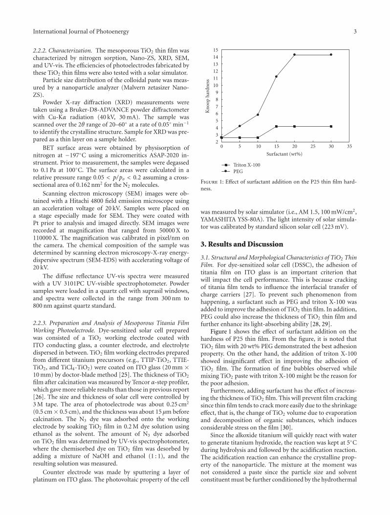
International Journal of Photoenergy 3
2.2.2. Characterization. The mesoporous TiO2 thin film wascharacterized by nitrogen sorption, Nano-ZS, XRD, SEM,and UV-vis. The efficiencies of photoelectrodes fabricated bythese TiO2 thin films were also tested with a solar simulator.
Particle size distribution of the colloidal paste was meas-ured by a nanoparticle analyzer (Malvern zetasizer Nano-ZS).
Powder X-ray diffraction (XRD) measurements weretaken using a Bruker-D8-ADVANCE powder diffractometerwith Cu-Kα radiation (40 kV, 30 mA). The sample wasscanned over the 2θ range of 20–60◦ at a rate of 0.05◦ min−1
to identify the crystalline structure. Sample for XRD was pre-pared as a thin layer on a sample holder.
BET surface areas were obtained by physisorption ofnitrogen at −197◦C using a micromeritics ASAP-2020 in-strument. Prior to measurement, the samples were degassedto 0.1 Pa at 100◦C. The surface areas were calculated in arelative pressure range 0.05 < p/po < 0.2 assuming a cross-sectional area of 0.162 nm2 for the N2 molecules.
Scanning electron microscopy (SEM) images were ob-tained with a Hitachi 4800 field emission microscope usingan acceleration voltage of 20 kV. Samples were placed ona stage especially made for SEM. They were coated withPt prior to analysis and imaged directly. SEM images wererecorded at magnification that ranged from 50000 X to110000 X. The magnification was calibrated in pixel/nm onthe camera. The chemical composition of the sample wasdetermined by scanning electron microscopy-X-ray energy-dispersive spectrum (SEM-EDS) with accelerating voltage of20 kV.
The diffuse reflectance UV-vis spectra were measuredwith a UV 3101PC UV-visible spectrophotometer. Powdersamples were loaded in a quartz cell with suprasil windows,and spectra were collected in the range from 300 nm to800 nm against quartz standard.
2.2.3. Preparation and Analysis of Mesoporous Titania FilmWorking Photoelectrode. Dye-sensitized solar cell preparedwas consisted of a TiO2 working electrode coated withITO conducting glass, a counter electrode, and electrolytedispersed in between. TiO2 film working electrodes preparedfrom different titanium precursors (e.g., TTIP-TiO2, TTIE-TiO2, and TiCl4-TiO2) were coated on ITO glass (20 mm ×10 mm) by doctor-blade method [25]. The thickness of TiO2
film after calcination was measured by Tencor α-step profiler,which gave more reliable results than those in previous report[26]. The size and thickness of solar cell were controlled by3 M tape. The area of photoelectrode was about 0.25 cm2
(0.5 cm × 0.5 cm), and the thickness was about 15 μm beforecalcination. The N3 dye was adsorbed onto the workingelectrode by soaking TiO2 film in 0.2 M dye solution usingethanol as the solvent. The amount of N3 dye adsorbedon TiO2 film was determined by UV-vis spectrophotometer,where the chemisorbed dye on TiO2 film was desorbed byadding a mixture of NaOH and ethanol (1 : 1), and theresulting solution was measured.
Counter electrode was made by sputtering a layer ofplatinum on ITO glass. The photovoltaic property of the cell
Triton X-100PEG
35302520151050
Surfactant (wt%)
2
3
4
5
6
7
8
9
10
11
12
13
14
15
Kn
oop
hard
nes
s
Figure 1: Effect of surfactant addition on the P25 thin film hard-ness.
was measured by solar simulator (i.e., AM 1.5, 100 mW/cm2,YAMASHITA YSS-80A). The light intensity of solar simula-tor was calibrated by standard silicon solar cell (223 mV).
3. Results and Discussion
3.1. Structural and Morphological Characteristics of TiO2 ThinFilm. For dye-sensitized solar cell (DSSC), the adhesion oftitania film on ITO glass is an important criterion thatwill impact the cell performance. This is because crackingof titania film tends to influence the interfacial transfer ofcharge carriers [27]. To prevent such phenomenon fromhappening, a surfactant such as PEG and triton X-100 wasadded to improve the adhesion of TiO2 thin film. In addition,PEG could also increase the thickness of TiO2 thin film andfurther enhance its light-absorbing ability [28, 29].
Figure 1 shows the effect of surfactant addition on thehardness of P25 thin film. From the figure, it is noted thatTiO2 film with 20 wt% PEG demonstrated the best adhesionproperty. On the other hand, the addition of triton X-100showed insignificant effect in improving the adhesion ofTiO2 film. The formation of fine bubbles observed whilemixing TiO2 paste with triton X-100 might be the reason forthe poor adhesion.
Furthermore, adding surfactant has the effect of increas-ing the thickness of TiO2 film. This will prevent film crackingsince thin film tends to crack more easily due to the shrinkageeffect, that is, the change of TiO2 volume due to evaporationand decomposition of organic substances, which inducesconsiderable stress on the film [30].
Since the alkoxide titanium will quickly react with waterto generate titanium hydroxide, the reaction was kept at 5◦Cduring hydrolysis and followed by the acidification reaction.The acidification reaction can enhance the crystalline prop-erty of the nanoparticle. The mixture at the moment wasnot considered a paste since the particle size and solventconstituent must be further conditioned by the hydrothermal
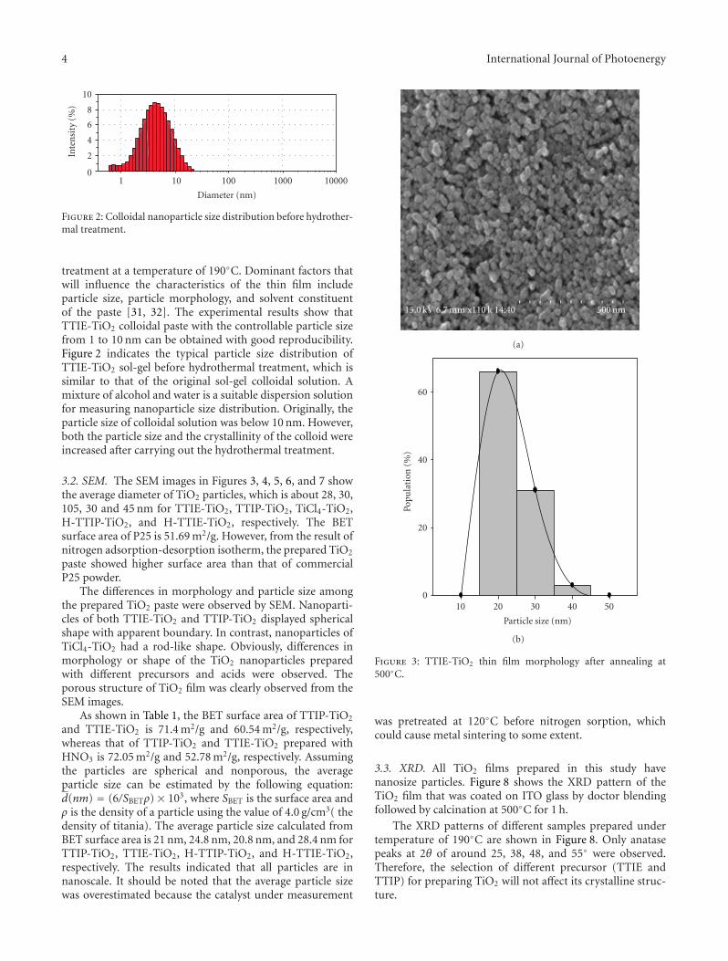
4 International Journal of Photoenergy
100001000100101
Diameter (nm)
0
2
4
6
8
10
Inte
nsi
ty(%
)
Figure 2: Colloidal nanoparticle size distribution before hydrother-mal treatment.
treatment at a temperature of 190◦C. Dominant factors thatwill influence the characteristics of the thin film includeparticle size, particle morphology, and solvent constituentof the paste [31, 32]. The experimental results show thatTTIE-TiO2 colloidal paste with the controllable particle sizefrom 1 to 10 nm can be obtained with good reproducibility.Figure 2 indicates the typical particle size distribution ofTTIE-TiO2 sol-gel before hydrothermal treatment, which issimilar to that of the original sol-gel colloidal solution. Amixture of alcohol and water is a suitable dispersion solutionfor measuring nanoparticle size distribution. Originally, theparticle size of colloidal solution was below 10 nm. However,both the particle size and the crystallinity of the colloid wereincreased after carrying out the hydrothermal treatment.
3.2. SEM. The SEM images in Figures 3, 4, 5, 6, and 7 showthe average diameter of TiO2 particles, which is about 28, 30,105, 30 and 45 nm for TTIE-TiO2, TTIP-TiO2, TiCl4-TiO2,H-TTIP-TiO2, and H-TTIE-TiO2, respectively. The BETsurface area of P25 is 51.69 m2/g. However, from the result ofnitrogen adsorption-desorption isotherm, the prepared TiO2
paste showed higher surface area than that of commercialP25 powder.
The differences in morphology and particle size amongthe prepared TiO2 paste were observed by SEM. Nanoparti-cles of both TTIE-TiO2 and TTIP-TiO2 displayed sphericalshape with apparent boundary. In contrast, nanoparticles ofTiCl4-TiO2 had a rod-like shape. Obviously, differences inmorphology or shape of the TiO2 nanoparticles preparedwith different precursors and acids were observed. Theporous structure of TiO2 film was clearly observed from theSEM images.
As shown in Table 1, the BET surface area of TTIP-TiO2
and TTIE-TiO2 is 71.4 m2/g and 60.54 m2/g, respectively,whereas that of TTIP-TiO2 and TTIE-TiO2 prepared withHNO3 is 72.05 m2/g and 52.78 m2/g, respectively. Assumingthe particles are spherical and nonporous, the averageparticle size can be estimated by the following equation:d(nm) = (6/SBETρ)× 103, where SBET is the surface area andρ is the density of a particle using the value of 4.0 g/cm3( thedensity of titania). The average particle size calculated fromBET surface area is 21 nm, 24.8 nm, 20.8 nm, and 28.4 nm forTTIP-TiO2, TTIE-TiO2, H-TTIP-TiO2, and H-TTIE-TiO2,respectively. The results indicated that all particles are innanoscale. It should be noted that the average particle sizewas overestimated because the catalyst under measurement
15.0 kV 6.7 mm x110 k 14:40 500 nm
(a)
5040302010
Particle size (nm)
0
20
40
60
Popu
lati
on(%
)
(b)
Figure 3: TTIE-TiO2 thin film morphology after annealing at500◦C.
was pretreated at 120◦C before nitrogen sorption, whichcould cause metal sintering to some extent.
3.3. XRD. All TiO2 films prepared in this study havenanosize particles. Figure 8 shows the XRD pattern of theTiO2 film that was coated on ITO glass by doctor blendingfollowed by calcination at 500◦C for 1 h.
The XRD patterns of different samples prepared undertemperature of 190◦C are shown in Figure 8. Only anatasepeaks at 2θ of around 25, 38, 48, and 55◦ were observed.Therefore, the selection of different precursor (TTIE andTTIP) for preparing TiO2 will not affect its crystalline struc-ture.
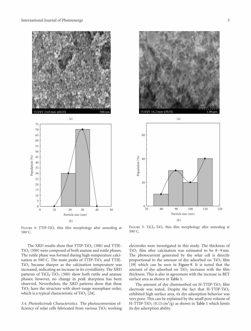
International Journal of Photoenergy 5
15.0 kV 14.8 mm x60.0 k 500 nm
(a)
50403020100
Particle size (nm)
0
5
10
15
20
25
30
35
40
45
50
55
60
65
70
75
Popu
lati
on(%
)
(b)
Figure 4: TTIP-TiO2 thin film morphology after annealing at500◦C.
The XRD results show that TTIP-TiO2 (500) and TTIE-TiO2 (500) were composed of both anatase and rutile phases.The rutile phase was formed during high-temperature calci-nation at 500◦C. The main peaks of TTIP-TiO2 and TTIE-TiO2 became sharper as the calcination temperature wasincreased, indicating an increase in its crystallinity. The XRDpatterns of TiCl4-TiO2 (500) show both rutile and anatasephases; however, no change in peak sharpness has beenobserved. Nevertheless, the XRD patterns show that theseTiO2 have the structure with short-range mesophase order,which is a typical characteristic of TiO2 [24].
3.4. Photoelectrode Characteristics. The photoconversion ef-ficiency of solar cells fabricated from various TiO2 working
15.0 kV 14.2 mm x30.0 k 1.00μm
(a)
120110100908070
Particle size (nm)
0
20
40
60Po
pula
tion
(%)
(b)
Figure 5: TiCI4-TiO2 thin film morphology after annealing at500◦C.
electrodes were investigated in this study. The thickness ofTiO2 film after calcination was estimated to be 8∼9 nm.The photocurrent generated by the solar cell is directlyproportional to the amount of dye adsorbed on TiO2 film[19] which can be seen in Figure 9. It is noted that theamount of dye adsorbed on TiO2 increases with the filmthickness. This is also in agreement with the increase in BETsurface area as shown in Table 1.
The amount of dye chemisorbed on H-TTIP-TiO2 filmelectrode was tested. Despite the fact that H-TTIP-TiO2
exhibited high surface area, its dye adsorption behavior wasvery poor. This can be explained by the small pore volume ofH-TTIP-TiO2 (0.13 cm3/g) as shown in Table 1 which limitsits dye adsorption ability.

6 International Journal of Photoenergy
15.0 kV 12.5 mm x150 k 300 nm
(a)
6050403020100
Particle size (nm)
0
10
20
30
40
50
60
Popu
lati
on(%
)
(b)
Figure 6: H-TTIP-TiO2 thin film morphology after annealing at500◦C.
The H-TTIE-TiO2 film prepared was composed mostlyof spherical primary particles and some ellipse-like sec-ondary particles. The use of TTIP precursor to reactwith different solvent and reactant will change the rate ofhydrolysis and primary particle growth [33]. In other words,the primary and secondary particle size, surface morphology,composition, and porosity of TiO2 will be influenced by theconcentration and type of precursor used.
Figure 10 shows photocurrent voltage characteristics ofthe cell made from various TiO2 calcined at 500◦C for 0.5 h.It is noted that the resistance of ITO conducting glass aftercalcination was increased to about 85∼110Ω. This will causea big impact on the efficiency of the solar cell since ITO
15.0 kV 12.5 mm x50.0 k 1.00μm
(a)
1009080706050403020
Particle size (nm)
0
10
20
30
40
50
60
Popu
lati
on(%
)
(b)
Figure 7: H-TTIE-TiO2 thin film morphology after annealing at500◦C.
functions to transfer electrons that are photogenerated fromdye-incorporated TiO2. From Table 2, it is obvious that thesolar cell made from TTIP-TiO2 thin film produces thelargest short-circuit current (Jsc).
High photocurrent could be generally related to highsurface area, which results in an increase in the amount of dyeadsorbed if the film thickness and light irradiation intensitywere kept constant. It might also be due to the presence ofmore anatase TiO2, which facilitates the electron transport[34]. This can be explained by the large pore size and highsurface area of TTIP-TiO2 electrode as revealed by SEM andBET analyses. In Tanaka’s study, as the titania particle getsbigger, the chance of electron/hole recombination gets lower

International Journal of Photoenergy 7
Table 2: Performances of various TiO2 thin film electrodes for DSSC.
Sample Thickness (μm) Jsc (mA/cm2) Voc (V) Fill factor η (%)
P25 10-11 ± 0.5 6.25 0.64 52.64 2.19
TTIE-TiO2 8-9 ± 0.5 5.63 0.70 62.18 2.45
H-TTIE-TiO2 8-9 ± 0.5 4.25 0.69 68.45 1.90
TTIP-TiO2 8-9 ± 0.5 13.13 0.76 44.96 4.45
H-TTIP-TiO2 8-9 ± 0.5 5.13 0.65 68.15 2.25
TiCl4-TiO2 8-9 ± 0.5 2.13 0.64 74.09 0.99
TTIP/TTIP∗ 15-16 ± 0.5 15.50 0.67 57.89 6.03∗
Double layer of TTIP-TiO2 for efficiency test.
AAA
A(110)R
R
RRR
(I)
(H)
(G)
(F)
(E)
(D)
(C)
(B)
(A)
(101)A
R
A-anataseR-rutile
6050403020
2θ (deg)
Inte
nsi
ty(a
.u.)
Figure 8: XRD patterns of TiO2 synthesized hydrothermally at190◦C for 12 h and calcinated at 500◦C for 0.5 h (A: TTIP (190),B: TTIE (190), C: H-TTIP (190), D: TTIP (500), E: TTIE (500), F:H-TTIP (500), G: H-TTIE (500), H: TiCl4 (500), I: P25).
[35]. The cell performance depends on the thickness of theTiO2 film. Therefore, we have made a double-layer TTIP-TiO2 thin film electrode that has a thickness of 16 μm [4]. Byincorporating this double-layer electrode into a solar cell, aphotoconversion efficiency as high as 6.03% can be reached.The sufficient film thickness will create large pore size andenough space which allow more redox electrolyte to diffuseinto the film.
TiCl4-TiO2 shows the highest surface area; however, itssolar energy conversion efficiency is only 0.99% with lowJsc of 2.13 mA/cm2. It is attributed to the poor adhesion ofTiO2 on ITO glass observed. The pH of TiCl4-TiO2 pasteis around 1∼2, which might cause a corrosion problem onITO conducting glass. Furthermore, TiCl4-TiO2 film showedpoor adhesion when immersed in the iodine electrolyteafter calcination. Although TiCl4-TiO2 showed poor perfor-mance, it displayed nanotube-like structure. If the adhesionproblem can be eliminated, low-cost and high-efficiencysolar cell may be fabricated.
151050
Thickness (μm)
0
2
4
6
8
10
12
10−8
(mol
e/cm
2)
TTIP-TiO2
P25H-TTIP-TiO2
TiCl4-TiO2
TTIE-TiO2
Figure 9: The amount of chemisorbed dye on the different thick-nesses.
0.70.60.50.40.30.20.10
Voltage (V)
0
0.0005
0.001
0.0015
0.002
Cu
rren
t(A
)
TTIETTIPTiCl4
H-TTIEH-TTIPP25
Figure 10: Photocurrent voltage characteristics of nanocrystallineTiO2 films prepared with different precursors.
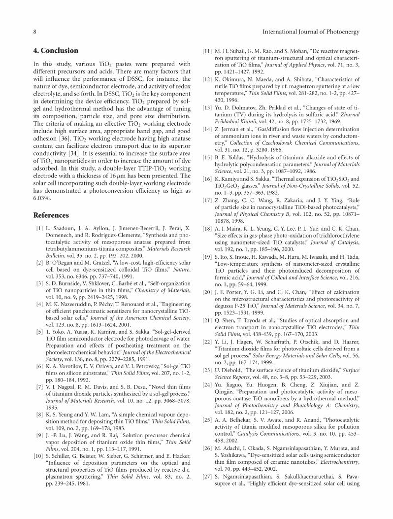
8 International Journal of Photoenergy
4. Conclusion
In this study, various TiO2 pastes were prepared withdifferent precursors and acids. There are many factors thatwill influence the performance of DSSC, for instance, thenature of dye, semiconductor electrode, and activity of redoxelectrolyte, and so forth. In DSSC, TiO2 is the key componentin determining the device efficiency. TiO2 prepared by sol-gel and hydrothermal method has the advantage of tuningits composition, particle size, and pore size distribution.The criteria of making an effective TiO2 working electrodeinclude high surface area, appropriate band gap, and goodadhesion [36]. TiO2 working electrode having high anatasecontent can facilitate electron transport due to its superiorconductivity [34]. It is essential to increase the surface areaof TiO2 nanoparticles in order to increase the amount of dyeadsorbed. In this study, a double-layer TTIP-TiO2 workingelectrode with a thickness of 16 μm has been presented. Thesolar cell incorporating such double-layer working electrodehas demonstrated a photoconversion efficiency as high as6.03%.
References
[1] L. Saadoun, J. A. Ayllon, J. Jimenez-Becerril, J. Peral, X.Domenech, and R. Rodriguez-Clemente, “Synthesis and pho-tocatalytic activity of mesoporous anatase prepared fromtetrabutylammonium-titania composites,” Materials ResearchBulletin, vol. 35, no. 2, pp. 193–202, 2000.
[2] B. O’Regan and M. Gratzel, “A low-cost, high-efficiency solarcell based on dye-sensitized colloidal TiO films,” Nature,vol. 353, no. 6346, pp. 737–740, 1991.
[3] S. D. Burnside, V. Shklover, C. Barbe et al., “Self-organizationof TiO nanoparticles in thin films,” Chemistry of Materials,vol. 10, no. 9, pp. 2419–2425, 1998.
[4] M. K. Nazeeruddin, P. Pechy, T. Renouard et al., “Engineeringof efficient panchromatic sensitizers for nanocrystalline TiO-based solar cells,” Journal of the American Chemical Society,vol. 123, no. 8, pp. 1613–1624, 2001.
[5] T. Yoko, A. Yuasa, K. Kamiya, and S. Sakka, “Sol-gel-derivedTiO film semiconductor electrode for photocleavage of water.Preparation and effects of postheating treatment on thephotoelectrochemical behavior,” Journal of the ElectrochemicalSociety, vol. 138, no. 8, pp. 2279–2285, 1991.
[6] K. A. Vorotilov, E. V. Orlova, and V. I. Petrovsky, “Sol-gel TiOfilms on silicon substrates,” Thin Solid Films, vol. 207, no. 1-2,pp. 180–184, 1992.
[7] V. J. Nagpal, R. M. Davis, and S. B. Desu, “Novel thin filmsof titanium dioxide particles synthesized by a sol-gel process,”Journal of Materials Research, vol. 10, no. 12, pp. 3068–3078,1995.
[8] K. S. Yeung and Y. W. Lam, “A simple chemical vapour depo-sition method for depositing thin TiO films,” Thin Solid Films,vol. 109, no. 2, pp. 169–178, 1983.
[9] J. -P. Lu, J. Wang, and R. Raj, “Solution precursor chemicalvapor deposition of titanium oxide thin films,” Thin SolidFilms, vol. 204, no. 1, pp. L13–L17, 1991.
[10] S. Schiller, G. Beister, W. Sieber, G. Schirmer, and E. Hacker,“Influence of deposition parameters on the optical andstructural properties of TiO films produced by reactive d.c.plasmatron sputtering,” Thin Solid Films, vol. 83, no. 2,pp. 239–245, 1981.
[11] M. H. Suhail, G. M. Rao, and S. Mohan, “Dc reactive magnet-ron sputtering of titanium-structural and optical characteri-zation of TiO films,” Journal of Applied Physics, vol. 71, no. 3,pp. 1421–1427, 1992.
[12] K. Okimura, N. Maeda, and A. Shibata, “Characteristics ofrutile TiO films prepared by r.f. magnetron sputtering at a lowtemperature,” Thin Solid Films, vol. 281-282, no. 1-2, pp. 427–430, 1996.
[13] Yu. D. Dolmatov, Zh. Priklad et al., “Changes of state of ti-tanium (TV) during its hydrolysis in sulfuric acid,” ZhurnalPrikladnoi Khimii, vol. 42, no. 8, pp. 1725–1732, 1969.
[14] Z. Jerman et al., “Gas/diffusion flow injection determinationof ammonium ions in river and waste waters by conductom-etry,” Collection of Czechoslovak Chemical Communications,vol. 31, no. 12, p. 3280, 1966.
[15] B. E. Yoldas, “Hydrolysis of titanium alkoxide and effects ofhydrolytic polycondensation parameters,” Journal of MaterialsScience, vol. 21, no. 3, pp. 1087–1092, 1986.
[16] K. Kamiya and S. Sakka, “Thermal expansion of TiO2SiO2 andTiO2GeO2 glasses,” Journal of Non-Crystalline Solids, vol. 52,no. 1–3, pp. 357–363, 1982.
[17] Z. Zhang, C. C. Wang, R. Zakaria, and J. Y. Ying, “Roleof particle size in nanocrystalline TiOi-based photocatalysts,”Journal of Physical Chemistry B, vol. 102, no. 52, pp. 10871–10878, 1998.
[18] A. J. Maira, K. L. Yeung, C. Y. Lee, P. L. Yue, and C. K. Chan,“Size effects in gas-phase photo-oxidation of trichloroethyleneusing nanometer-sized TiO catalysts,” Journal of Catalysis,vol. 192, no. 1, pp. 185–196, 2000.
[19] S. Ito, S. Inoue, H. Kawada, M. Hara, M. Iwasaki, and H. Tada,“Low-temperature synthesis of nanometer-sized crystallineTiO particles and their photoinduced decomposition offormic acid,” Journal of Colloid and Interface Science, vol. 216,no. 1, pp. 59–64, 1999.
[20] J. F. Porter, Y. G. Li, and C. K. Chan, “Effect of calcinationon the microstructural characteristics and photoreactivity ofdegussa P-25 TiO,” Journal of Materials Science, vol. 34, no. 7,pp. 1523–1531, 1999.
[21] Q. Shen, T. Toyoda et al., “Studies of optical absorption andelectron transport in nanocrystalline TiO electrodes,” ThinSolid Films, vol. 438-439, pp. 167–170, 2003.
[22] Y. Li, J. Hagen, W. Schaffrath, P. Otschik, and D. Haarer,“Titanium dioxide films for photovoltaic cells derived from asol gel process,” Solar Energy Materials and Solar Cells, vol. 56,no. 2, pp. 167–174, 1999.
[23] U. Diebold, “The surface science of titanium dioxide,” SurfaceScience Reports, vol. 48, no. 5–8, pp. 53–229, 2003.
[24] Yu. Jiaguo, Yu. Huogen, B. Cheng, Z. Xiujian, and Z.Qingjie, “Preparation and photocatalytic activity of meso-porous anatase TiO nanofibers by a hydrothermal method,”Journal of Photochemistry and Photobiology A: Chemistry,vol. 182, no. 2, pp. 121–127, 2006.
[25] A. A. Belhekar, S. V. Awate, and R. Anand, “Photocatalyticactivity of titania modified mesoporous silica for pollutioncontrol,” Catalysis Communications, vol. 3, no. 10, pp. 453–458, 2002.
[26] M. Adachi, I. Okada, S. Ngamsinlapasathian, Y. Murata, andS. Yoshikawa, “Dye-sensitized solar cells using semiconductorthin film composed of ceramic nanotubes,” Electrochemistry,vol. 70, pp. 449–452, 2002.
[27] S. Ngamsinlapasathian, S. Sakulkhaemaruethai, S. Pava-supree et al., “Highly efficient dye-sensitized solar cell using
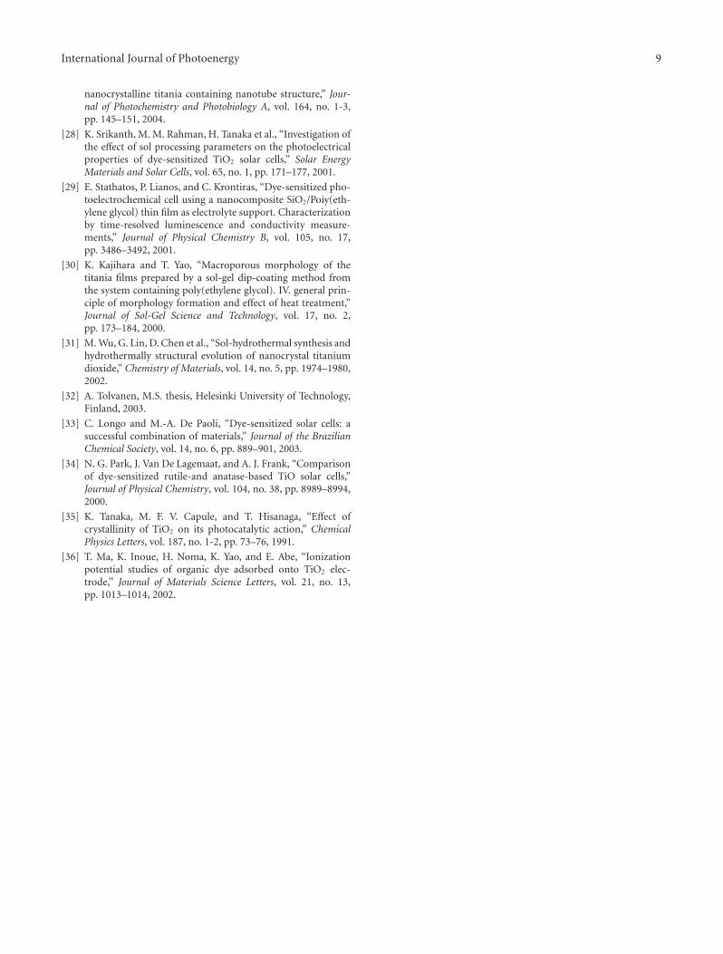
International Journal of Photoenergy 9
nanocrystalline titania containing nanotube structure,” Jour-nal of Photochemistry and Photobiology A, vol. 164, no. 1-3,pp. 145–151, 2004.
[28] K. Srikanth, M. M. Rahman, H. Tanaka et al., “Investigation ofthe effect of sol processing parameters on the photoelectricalproperties of dye-sensitized TiO2 solar cells,” Solar EnergyMaterials and Solar Cells, vol. 65, no. 1, pp. 171–177, 2001.
[29] E. Stathatos, P. Lianos, and C. Krontiras, “Dye-sensitized pho-toelectrochemical cell using a nanocomposite SiO2/Poiy(eth-ylene glycol) thin film as electrolyte support. Characterizationby time-resolved luminescence and conductivity measure-ments,” Journal of Physical Chemistry B, vol. 105, no. 17,pp. 3486–3492, 2001.
[30] K. Kajihara and T. Yao, “Macroporous morphology of thetitania films prepared by a sol-gel dip-coating method fromthe system containing poly(ethylene glycol). IV. general prin-ciple of morphology formation and effect of heat treatment,”Journal of Sol-Gel Science and Technology, vol. 17, no. 2,pp. 173–184, 2000.
[31] M. Wu, G. Lin, D. Chen et al., “Sol-hydrothermal synthesis andhydrothermally structural evolution of nanocrystal titaniumdioxide,” Chemistry of Materials, vol. 14, no. 5, pp. 1974–1980,2002.
[32] A. Tolvanen, M.S. thesis, Helesinki University of Technology,Finland, 2003.
[33] C. Longo and M.-A. De Paoli, “Dye-sensitized solar cells: asuccessful combination of materials,” Journal of the BrazilianChemical Society, vol. 14, no. 6, pp. 889–901, 2003.
[34] N. G. Park, J. Van De Lagemaat, and A. J. Frank, “Comparisonof dye-sensitized rutile-and anatase-based TiO solar cells,”Journal of Physical Chemistry, vol. 104, no. 38, pp. 8989–8994,2000.
[35] K. Tanaka, M. F. V. Capule, and T. Hisanaga, “Effect ofcrystallinity of TiO2 on its photocatalytic action,” ChemicalPhysics Letters, vol. 187, no. 1-2, pp. 73–76, 1991.
[36] T. Ma, K. Inoue, H. Noma, K. Yao, and E. Abe, “Ionizationpotential studies of organic dye adsorbed onto TiO2 elec-trode,” Journal of Materials Science Letters, vol. 21, no. 13,pp. 1013–1014, 2002.
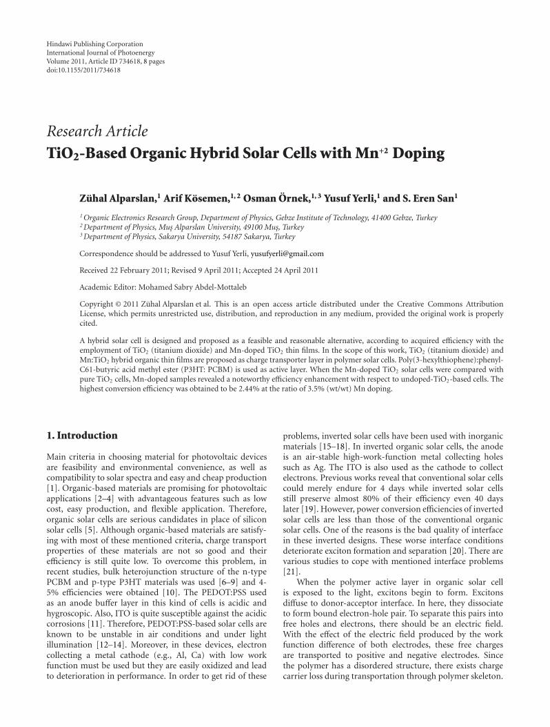
Hindawi Publishing CorporationInternational Journal of PhotoenergyVolume 2011, Article ID 734618, 8 pagesdoi:10.1155/2011/734618
Research Article
TiO2-Based Organic Hybrid Solar Cells with Mn+2 Doping
Zuhal Alparslan,1 Arif Kosemen,1, 2 Osman Ornek,1, 3 Yusuf Yerli,1 and S. Eren San1
1 Organic Electronics Research Group, Department of Physics, Gebze Institute of Technology, 41400 Gebze, Turkey2 Department of Physics, Mus Alparslan University, 49100 Mus, Turkey3 Department of Physics, Sakarya University, 54187 Sakarya, Turkey
Correspondence should be addressed to Yusuf Yerli, [email protected]
Received 22 February 2011; Revised 9 April 2011; Accepted 24 April 2011
Academic Editor: Mohamed Sabry Abdel-Mottaleb
Copyright © 2011 Zuhal Alparslan et al. This is an open access article distributed under the Creative Commons AttributionLicense, which permits unrestricted use, distribution, and reproduction in any medium, provided the original work is properlycited.
A hybrid solar cell is designed and proposed as a feasible and reasonable alternative, according to acquired efficiency with theemployment of TiO2 (titanium dioxide) and Mn-doped TiO2 thin films. In the scope of this work, TiO2 (titanium dioxide) andMn:TiO2 hybrid organic thin films are proposed as charge transporter layer in polymer solar cells. Poly(3-hexylthiophene):phenyl-C61-butyric acid methyl ester (P3HT: PCBM) is used as active layer. When the Mn-doped TiO2 solar cells were compared withpure TiO2 cells, Mn-doped samples revealed a noteworthy efficiency enhancement with respect to undoped-TiO2-based cells. Thehighest conversion efficiency was obtained to be 2.44% at the ratio of 3.5% (wt/wt) Mn doping.
1. Introduction
Main criteria in choosing material for photovoltaic devicesare feasibility and environmental convenience, as well ascompatibility to solar spectra and easy and cheap production[1]. Organic-based materials are promising for photovoltaicapplications [2–4] with advantageous features such as lowcost, easy production, and flexible application. Therefore,organic solar cells are serious candidates in place of siliconsolar cells [5]. Although organic-based materials are satisfy-ing with most of these mentioned criteria, charge transportproperties of these materials are not so good and theirefficiency is still quite low. To overcome this problem, inrecent studies, bulk heterojunction structure of the n-typePCBM and p-type P3HT materials was used [6–9] and 4-5% efficiencies were obtained [10]. The PEDOT:PSS usedas an anode buffer layer in this kind of cells is acidic andhygroscopic. Also, ITO is quite susceptible against the acidiccorrosions [11]. Therefore, PEDOT:PSS-based solar cells areknown to be unstable in air conditions and under lightillumination [12–14]. Moreover, in these devices, electroncollecting a metal cathode (e.g., Al, Ca) with low workfunction must be used but they are easily oxidized and leadto deterioration in performance. In order to get rid of these
problems, inverted solar cells have been used with inorganicmaterials [15–18]. In inverted organic solar cells, the anodeis an air-stable high-work-function metal collecting holessuch as Ag. The ITO is also used as the cathode to collectelectrons. Previous works reveal that conventional solar cellscould merely endure for 4 days while inverted solar cellsstill preserve almost 80% of their efficiency even 40 dayslater [19]. However, power conversion efficiencies of invertedsolar cells are less than those of the conventional organicsolar cells. One of the reasons is the bad quality of interfacein these inverted designs. These worse interface conditionsdeteriorate exciton formation and separation [20]. There arevarious studies to cope with mentioned interface problems[21].
When the polymer active layer in organic solar cellis exposed to the light, excitons begin to form. Excitonsdiffuse to donor-acceptor interface. In here, they dissociateto form bound electron-hole pair. To separate this pairs intofree holes and electrons, there should be an electric field.With the effect of the electric field produced by the workfunction difference of both electrodes, these free chargesare transported to positive and negative electrodes. Sincethe polymer has a disordered structure, there exists chargecarrier loss during transportation through polymer skeleton.

2 International Journal of Photoenergy
Inorganic materials are used with organics so that orderedcontinuous paths are provided to charge transfer. This kindof designs are called hybrid systems, and for this aim, variousinorganic materials are used in solar cells such as ZnO [22],CdTe [23], PbS [24], and so forth. TiO2 [20, 25, 26] is alsoan attractive alternative among these materials. Usage ofTiO2 electrode in dye-based solar cell by Gratzel et al. couldbe given as a successful application of this material [27].There are various works to understand the structural changesoccurred when TiO2 is doped by metal ions. In particular,photocatalytic and magnetic properties were investigatedby [28, 29]. In the result of such investigations, it wasunderstood that photoreactivity, charge carrier recombina-tion rates, and interfacial electron transfer rates were changedby metal ion doping [30]. Doped TiO2 is widely used in solarcell applications, and there are several comparative works.In one of them, it has been reported that power conversionefficiency was achieved to be 8% with the dye-based solarcells prepared by nitrogen-doped TiO2 while 6% efficiencywith pure TiO2 [31]. Also, K. H. Ko et al. performed anotherwork in which TiO2 was doped with Al and W elements fordye-based solar cells. In Al-doped cells, while open-circuitvoltage (VOC) has increased, short-circuit current (ISC) hasdecreased. As for W-doped cells, a behavior opposite to Al-doped cells was observed [32].
In this work, hybrid solar cells were produced and char-acterized with ITO/TiO2/P3HT : PCBM/Ag configuration.The novelty and goal of this work comes from the employ-ment of Mn+2 ions for the first time with this configuration,in which different amounts of Mn were incorporated toTiO2and cell parameters were investigated in terms of dopingamount. It was explicitly observed that solar cell efficiencywas being improved with Mn doping until a certain dopingamount, which is 3.5%. One of the inspirations of choosingMn+2 ion in our aim comes from some works such as [33],which reveals the fact that although the Mn+2 ion is slightlylarger than Ti+4, the general crystal structure is not changedwith doping but light interaction of modified TiO2.
2. Experimental
P3HT (Aldrich) and PCBM (Aldrich) were used in the struc-ture of active layer without any further purification. Theirchemical formulas are given in Figure 1. P3HT and PCBMwere firstly mixed in chlorobenzene with 1 : 0.8 (wt/wt)ratio at 60◦C for a night. In order to prepare TiO2 sol-gelmixture, titanium n-butoxide, ethanol, isopropanol alcohol,and acetic acid were mixed with (1 : 20 : 20 : 0.15) molar ratio,respectively, for two days at room temperature. Also, MnCl2was added into a solution containing a mixture of ethanol,isopropanol alcohol, and acetic acid. This solution of mixturewas stirred for two hours at room temperature, and thentitanium n-butoxide was added to this sol-gel mixture sothat Mn-doped TiO2 sample was prepared. Ti amount in thesolution of mixture is proportional to the amount of Mn,at ratio of their weights. The Mn amounts in samples wereprepared as 0.5%, 1.5%, 3.5%, 8.5%, 15%, and 25%.
In regard to the solar cell fabrication process, ITO-coated glass was firstly subject to a standard cleaning process
S
CH2(CH2)4CH3
n
(a)
O
OCH3
(b)
Figure 1: Chemical formulas of (a) P3HT and (b) PCBM.
MnMnMn
MnMnMn
4 0 0 5 0 0 6 0 0 7 0 0 8 0 0 9 0 0 1 0 0 0 1 1 0 0
( n m )
0
0 . 1
0 . 2
0 . 3
0 . 4
0 . 5
0 . 6
0 . 7
0 . 8
Ab s
o r b a
n c e
( a .
u . )
0 % Mn d o p e d 0 . 5 % d o p e d 1 . 5 % d o p e d 3 . 5 % d o p e d
8 . 5 % d o p e d 1 5 % d o p e d 2 5 % d o p e d
Figure 2: Absorption spectra of pure, 0.5%, 1.5%, 3.5%, 8.5%,15%, and 25% doped TiO2 films.
with acetone, ethanol, and distilled water in ultrasonicbath for 15 minutes to each cleaning agent. Later, TiO2-and Mn-doped TiO2 gels were coated with spin coaterat 3500 rpm. These thin films were annealed at 400◦Cfor 30 min, which was reached in steps of 10◦C/min. Thesolar cells were designed with ITO/TiO2/P3HT : PCBM/Agand ITO/TiO2 : Mn/P3HT : PCBM/Ag configuration. TiO2
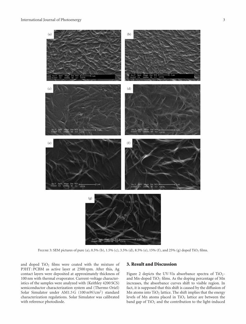
International Journal of Photoenergy 3
(a) (b)
(d)(c)
(f)
(g)
(e)
Ac c . V 1 0 . 0 k V
S p o t 3.0
M a g n 1 6 0 0 0 x
D e t S E
W D 5 . 7 G Y T E
2μmAc c . V 1 0 . 0 k V
S p o t 3.0
M a g n 1 6 0 0 0 x
D e t S E
W D 5 . 7 G Y T E
2μm
Ac c . V 1 5 . 0 k V
S p o t 3.0
M a g n 2 5 0 0 0 x
D e t S E
W D 5 . 4 G Y T E
2μmAcc.V15.0 kV
Spot3.0
Magn25000x
DetSE
WD5.4 GYTE
2μm
Ac c . V 1 5 . 0 k V
S p o t 3.0
M a g n 2 5 0 0 0 x
D e t S E
W D 5 . 3 G Y T E
2μmAc c . V 1 5 . 0 k V
S p o t 3.0
M a g n 2 5 0 0 0 x
D e t S E
W D 5 . 2 G Y T E
2μm
Ac c . V 1 5 . 0 k V
S p o t 3.0
M a g n 2 5 0 0 0 x
D e t S E
W D 5 . 4 G Y T E
2μm
Figure 3: SEM pictures of pure (a), 0.5% (b), 1.5% (c), 3.5% (d), 8.5% (e), 15% (f), and 25% (g) doped TiO2 films.
and doped TiO2 films were coated with the mixture ofP3HT : PCBM as active layer at 2500 rpm. After this, Agcontact layers were deposited at approximately thickness of100 nm with thermal evaporator. Current-voltage character-istics of the samples were analyzed with (Keithley 4200 SCS)semiconductor characterization system and (Thermo Oriel)Solar Simulator under AM1.5 G (100 mW/cm2) standardcharacterization regulations. Solar Simulator was calibratedwith reference photodiode.
3. Result and Discussion
Figure 2 depicts the UV-Vis absorbance spectra of TiO2-and Mn-doped TiO2 films. As the doping percentage of Mnincreases, the absorbance curves shift to visible region. Infact, it is supposed that this shift is caused by the diffusion ofMn atoms into TiO2 lattice. The shift implies that the energylevels of Mn atoms placed in TiO2 lattice are between theband gap of TiO2 and the contribution to the light-induced

4 International Journal of Photoenergy
−2 −1 0 1 2
Po t ant i a l ( V o l t )
0
5
1 0
1 5
20
J( m
A / c
m 2)
0 % M n 0 . 5 % M n 1 . 5 % M n 3 . 5 % M n
8 . 5 % M n 1 5 % M n 2 5 % M n
D a r k c u r v e s b e f o r e i l l u m i n a t i o n
Figure 4: J-V characteristic curves for TiO2- and Mn-doped TiO2
solar cells under dark circumstances (before any illuminationprocess).
−2 −1 0 1 2
Po t an t i a l ( V o l t )
J( m
A / c
m 2)
0% Mn0.5% Mn1.5% Mn3.5% Mn
8.5% Mn15% Mn25% Mn
0
2 0
4 0
6 0
8 0
100
D a r k c u r v e s a f t e r i l l u m i n a t i o n
Figure 5: J-V characteristic curves for TiO2- and Mn-doped TiO2
solar cells under dark circumstances (after 60-minute illumination).
charge transfer [34]. Also, these kinds of red shifts are relatedto the charge transfer between d-electrons of metal ions andvalance or conduction band of TiO2 [35]. The SEM picturesof TiO2- and Mn-doped TiO2 films are given in Figure 3.The SEM pictures show the growing of weak skeletons in thecase of Pure TiO2 as shown in Figure 3(a). As the Mn dopingpercentage is further increased, branches of the skeleton aregetting stronger and these stronger branches are yielding an
obvious fiber structures particularly as seen in Figures 3(f)and 3(g).
Figure 4 shows the dark J-V characteristic curves ofsolar cells prepared by Mn-doped and pure TiO2 films. Theforward bias current of pure-TiO2-based cells is bigger thanthat of the Mn-based cells. That is, injection current is morein pure TiO2 cells. This indicates the presence of an injectionbarrier imposed by Mn doping. The same cells are subjectto the same measurements under dark conditions again,but this time these cells are exposed to illumination for60 minutes before dark J-V measurements (Figure 5). Thistime, the obtained results are entirely different from previousmeasurements. Forward bias current has increased in allcells, but this increase is much more in 0.5%, 1.5%, 3.5%, and8.5% doping percentages. In the case of 15% and 25% Mn-doped TiO2 cells, the increasing tendency of the forward biascurrent is disrupted. This indicates that there is a thresholdvalue of the Mn doping in our solar cell design. When thecells are exposed to illumination, both photoexcitation andthermal-excitation play an important role in increasing thenumber of charge carriers in (P3HT : PCBM) active layer andhighly photoreactive TiO2 layers. This could be recognizedto be the cause of the increase in current. Also, the injectionbarrier mentioned for the Mn-doped cells is eliminated whenthe cells are waited under illumination, so forward biascurrents are becoming more with respect to the pure TiO2
based cells.The highest forward bias current and maximum power
conversion efficiency were observed in 3.5% Mn-doped solarcell. The J-V plots of pure TiO2 and Mn-doped TiO2-based solar cells under illuminated conditions are shownin Figure 6. The power conversion efficiency parametersobtained from these graphs are given in Table 1. There isno improvement in the pure TiO2 solar cell when the cell issubject to a light illumination even if forward bias currentslightly changes due to the heating of the cell. Whereas,even very little amount of Mn doping, for example 0.5%,causes an S-shape in reverse bias in the J-V curves, as soonas illumination starts. In this study as the solar cells wereexposed to continuous illumination, the S-shape disappears.After two minutes, it converted conventional solar cell shapefor % 0.5 Mn doped. This was observed in all Mn-dopedTiO2 cells. In a work, this kind of S-shape curves waspreviously explained with electrical dipoles occurred at theinterface [36]. In another study, it is expressed that the reasonfor S-shaped curve is charge accumulation near one of theelectrodes [37]. As for our cells, the reason for S-shapedcurve (Figure 6) was the accumulation of the charge occuringin TiO2 due to Mn doping.
ITO/TiO2/P3HT : PCBM/Ag solar cells are actually theinverted structures, and light is absorbed in P3HT activelayer. The excitons, which are produced in polymer activelayer, are separated at P3HT/PCBM interface, and freeelectrons are diffused to ITO side by passing throughTiO2while the free holes are diffused to Ag side as representedin Figure 7. It is obvious that the reason of S-shaped curve isthe Mn(II) ions, since there is no such a shape in pure-TiO2-containing cells, as seen in Figure 6. In regard to possiblemechanism of this event, one can think that either the
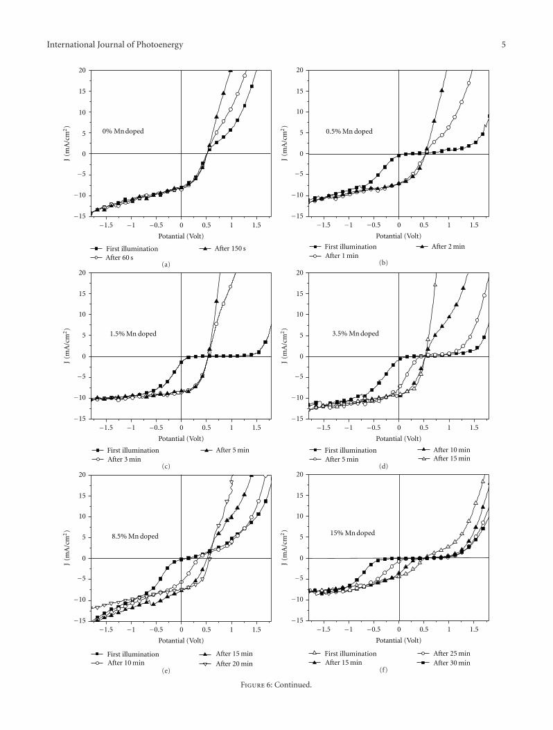
International Journal of Photoenergy 5
−1 0 0 . 5 1 1 . 5
Po t an t i a l ( V o l t )
−1 5
−1 0
−5
0
5
1 0
1 5
20J
( m A
/ c m
2)
First illuminationAfter 60 s
After 150 s
−1 . 5 −0 . 5
0% Mn doped
(a)
−1 0 0 . 5 1 1 . 5
Po t an t i a l ( V o l t )
−1 5
−1 0
−5
0
5
1 0
1 5
20
J( m
A / c
m 2)
First illumination
−1 . 5 −0 . 5
After 1 minAfter 2 min
Mn0.5% doped
(b)
−1 0 0 . 5 1 1 . 5
Po t ant i a l ( V o l t )
−1 5
−1 0
−5
0
5
1 0
1 5
20
J( m
A / c
m 2)
First illumination
−1 . 5 −0 . 5
After 3 minAfter 5 min
Mn1.5% doped
(c)
−1 0 0 . 5 1 1 . 5
Po t an t i a l ( V o l t )
−1 5
−1 0
−5
0
5
1 0
1 5
20
J( m
A / c
m 2)
First illumination
−1 . 5 −0 . 5
After 5 min After 15 minAfter 10 min
Mn3.5% doped
(d)
−1 0 0 . 5 1 1 . 5
Po t an t i a l ( V o l t )
−1 5
−1 0
−5
0
5
1 0
1 5
20
J( m
A / c
m 2)
First illumination
−1 . 5 −0 . 5
After 20 minAfter 10 minAfter 15 min
Mn8.5% doped
(e)
−1 0 0 . 5 1 1 . 5
Po t an t i a l ( V o l t )
−1 5
−1 0
−5
0
5
1 0
1 5
20
J( m
A / c
m 2)
First illumination
−1 . 5 −0 . 5
After 30 minAfter 15 minAfter 25 min
Mn15% doped
(f)
Figure 6: Continued.
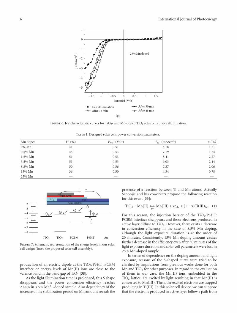
6 International Journal of Photoenergy
−1 0 0 . 5 1 1 . 5
Po t an t i a l ( V o l t )
−4
−3
−2
−1
0
1
−5
J( m
A / c
m 2)
F i r s t i l l u m i n a t i o n
−1 . 5 −0 . 5
A f t e r 4 5 m i n A f te r 1 5 m i n
A f t e r 3 0 m i n
Mn25% doped
(g)
Figure 6: J-V characteristic curves for TiO2- and Mn-doped TiO2 solar cells under illumination.
Table 1: Designed solar cells power conversion parameters.
Mn doped FF (%) VOC (Volt) ISC (mA/cm2) η (%)
0% Mn 41 0.51 8.18 1.71
0.5% Mn 45 0.53 7.19 1.74
1.5% Mn 51 0.53 8.41 2.27
3.5% Mn 51 0.53 9.03 2.44
8.5% Mn 50 0.56 7.37 2.06
15% Mn 36 0.50 4.34 0.78
25% Mn — — — —
ITO
TiO Glass substrate
P3HT:PCBM
TiO2
T i O 2 P C B M P 3 H T A g
A g
+
−8
−7
−6
−5
−4
−3
−2
h
−
+
−−−−
Figure 7: Schematic representation of the energy levels in our solarcell design (inset: the proposed solar cell assembly).
production of an electric dipole at the TiO2/P3HT : PCBMinterface or energy levels of Mn(II) ions are close to thevalance band in the band gap of TiO2 [38].
As the light illumination time is prolonged, this S shapedisappears and the power conversion efficiency reaches2.44% in 3.5% Mn2+-doped sample. Also dependency of theincrease of the stabilization period on Mn amount reveals the
presence of a reaction between Ti and Mn atoms. ActuallySaponjic and his coworkers propose the following reactionfor this event [33]:
TiO2 : Mn(II) ⇐⇒hv
Mn(III) + xe−cb + (1− x)Ti(III)latt (1)
For this reason, the injection barrier of the TiO2/P3HT:PCBM interface disappears and those electrons produced inactive layer diffuse to TiO2. However, there exists a decreasein conversion efficiency in the case of 8.5% Mn doping,although the light exposure duration is at the order of20 minutes. Consistently, 15% Mn doping amount causesfurther decrease in the efficiency even after 30 minutes of thelight exposure duration and solar cell parameters were lost in25% Mn-doped sample.
In terms of dependence on the doping amount and lightexposure, reasons of the S-shaped curve were tried to beclarified by inspirations from previous works done for bothMn and TiO2 for other purposes. In regard to the evaluationof them in our case, the Mn(II) ions, embedded in theTiO2 lattice, are excited by light resulting in that Mn(II) isconverted to Mn(III). Then, the excited electrons are trappedproducing in Ti(III). In this solar cell device, we can supposethat the electrons produced in active layer follow a path from

International Journal of Photoenergy 7
the TiO2 to the ITO. As the light falls on the cell, the Mn(III) traps in the TiO2 lattice occur for the electrons from theactive layer. These electrons should pass to ITO side, but Mn(III) traps in the TiO2 lattice capture them. The real reasonof the observed S-shaped curve can be these Mn (III) traps.As long as the device is waited under the light illumination,electrons fill these trap levels. After the filling of the traplevels, the electrons transfer towards ITO effectively. In ouropinion, the use of transition metal ions in hybrid solar cellis a serious candidate for the applications according to theresults obtained experimentally.
4. Conclusion
The goal of this work is to exploit transition metal ions inhybrid organic solar cell. The Mn(II) ions were successfullyadapted to TiO2-based solar cells for the first time.
The S-like shape, which is observed occasionally, in theproposed solar cells, is attained in the scope of our hybriddesign. The S-like shape is dependent on the Mn dopingamounts and light exposure time (it disappears after longexposure time) for yielding an efficient solar cell. Maximumpower conversion efficiency was obtained to be η = 2.44%for 3.5% Mn-doped TiO2 solar cell. Isc value is consideredto be 9.03 mA/cm2, which is a maximum in this efficient celland Voc value is 0.53 V, which is a constant in all cells. Thisefficient cell reaches stability after 10-minute illumination.But further doping with Mn(II) ions resulted in decayingof the efficiency despite having longer stability periods. 25%Mn-doped cell could not reach desired stability and the cellparameters could not be measured for it even after 45-minuteillumination.
References
[1] A. P. Zoombelt, M. Fonrodona, M. M. Wienk, A. B. Sieval, J. C.Hummelen, and R. A. J. Janssen, “Photovoltaic performance ofan ultrasmall band gap polymer,” Organic Letters, vol. 11, no.4, pp. 903–906, 2009.
[2] C. J. Brabec, N. S. Sariciftci, and J. C. Hummelen, “Plastic solarcells,” Advanced Funtional Materials, vol. 11, no. 1, pp. 15–26,2001.
[3] S. Gunes, H. Neugebauer, and N. S. Sariciftci, “Conjugatedpolymer-based organic solar cells,” Chemical Reviews, vol. 107,no. 4, pp. 1324–1338, 2007.
[4] H. Spanggaard and F. C. Krebs, “A brief history of thedevelopment of organic and polymeric photovoltaics,” SolarEnergy Materials and Solar Cells, vol. 83, no. 2-3, pp. 125–146,2004.
[5] J. Kalowekamo and E. Baker, “Estimating the manufacturingcost of purely organic solar cells,” Solar Energy, vol. 83, no. 8,pp. 1224–1231, 2009.
[6] N. S. Sariciftci, L. Smilowitz, A. J. Heeger, and F. Wudl,“Photoinduced electron transfer from a conducting polymerto buckminsterfullerene,” Science, vol. 258, no. 5087, pp. 1474–1476, 1992.
[7] M. M. Wienk, M. G. R. Turbiez, M. P. Struijk, M. Fon-rodona, and R. A. J. Janssen, “Low-band gap poly(di-2-thienylthienopyrazine): fullerene solar cells,” Applied PhysicsLetters, vol. 88, no. 15, Article ID 153511, 2006.
[8] N. Camaioni, G. Ridolfi, G. Casalbore-Miceli, G. Possamai,and M. Maggini, “The effect of a mild thermal treatmenton the performance of poly(3-alkylthiophene)/fullerene solarcells,” Advanced Materials, vol. 14, no. 23, pp. 1735–1738,2002.
[9] J. K. J. van Duren, X. Yang, J. Loos et al., “Relating themorphology of poly(p-phenylene vinylene)/methanofullereneblends to solar-cell performance,” Advanced Functional Mate-rials, vol. 14, no. 5, pp. 425–434, 2004.
[10] M. Reyes-Reyes, K. Kim, and D. L. Carroll, “High-efficiencyphotovoltaic devices based on annealed poly(3-hexylthiophe-ne) and 1-(3-methoxycarbonyl)-propyl-1- phenyl-(6,6)C61
blends,” Applied Physics Letters, vol. 87, no. 8, Article ID083506, 3 pages, 2005.
[11] H. Yan, P. Lee, N. R. Armstrong et al., “High-performancehole-transport layers for polymer light-emitting diodes.Implementation of organosiloxane cross-linking chemistry inpolymeric electroluminescent devices,” Journal of the Ameri-can Chemical Society, vol. 127, no. 9, pp. 3172–3183, 2005.
[12] K. Kawano, R. Pacios, D. Poplavskyy, J. Nelson, D. D. C.Bradley, and J. R. Durrant, “Degradation of organic solar cellsdue to air exposure,” Solar Energy Materials and Solar Cells,vol. 90, no. 20, pp. 3520–3530, 2006.
[13] N. Koch, A. Vollmer, and A. Elschner, “Influence of water onthe work function of conducting poly(3,4- ethylenedioxythio-phene)/poly(styrenesulfonate),” Applied Physics Letters, vol.90, no. 4, Article ID 043512, 2007.
[14] M. P. de Jong, L. J. van Ijzendoorn, and M. J. A. de Voigt, “Sta-bility of the interface between indium-tin-oxide and poly(3,4-ethylenedioxythiophene)/poly(styrenesulfonate) in polymerlight-emitting diodes,” Applied Physics Letters, vol. 77, no. 14,pp. 2255–2257, 2000.
[15] A. C. Arango, L. R. Johnson, V. N. Bliznyuk, Z. Schlesinger, S.A. Carter, and H. H. Horhold, “Efficient titanium oxide/con-jugated polymer photovoltaics for solar energy conversion,”Advanced Materials, vol. 12, no. 22, pp. 1689–1692, 2000.
[16] Y. Liu, M. A. Summers, C. Edder, J. M. J. Frechet, and M.D. McGehee, “Using resonance energy transfer to improveexciton harvesting in organic-inorganic hybrid photovoltaiccells,” Advanced Materials, vol. 17, no. 24, pp. 2960–2964,2005.
[17] J. Owen, M. S. Son, K. H. Yoo, B. D. Ahn, and S. Y. Lee,“Organic photovoltaic devices with Ga-doped ZnO electrode,”Applied Physics Letters, vol. 90, no. 3, Article ID 033512, 2007.
[18] C. Waldauf, M. Morana, P. Denk et al., “Highly efficientinverted organic photovoltaics using solution based titaniumoxide as electron selective contact,” Applied Physics Letters, vol.89, no. 23, Article ID 233517, 2006.
[19] S. K. Hau, H. L. Yip, N. S. Baek, J. Zou, K. O’Malley, and A.K. Y. Jen, “Air-stable inverted flexible polymer solar cells usingzinc oxide nanoparticles as an electron selective layer,” AppliedPhysics Letters, vol. 92, no. 25, Article ID 253301, 2008.
[20] W. H. Baek, I. Seo, T. S. Yoon, H. H. Lee, C. M. Yun, and Y.S. Kim, “Hybrid inverted bulk heterojunction solar cells withnanoimprinted TiO2 nanopores,” Solar Energy Materials andSolar Cells, vol. 93, no. 9, pp. 1587–1591, 2009.
[21] S. K. Hau, H. L. Yip, O. Acton, N. S. Baek, H. Ma, and A. K.Y. Jen, “Interfacial modification to improve inverted polymersolar cells,” Journal of Materials Chemistry, vol. 18, no. 42, pp.5113–5119, 2008.
[22] Y. Hames, Z. Alpaslan, A. Kosemen, S. E. San, and Y. Yerli,“Electrochemically grown ZnO nanorods for hybrid solar cellapplications,” Solar Energy, vol. 84, no. 3, pp. 426–431, 2010.
8 International Journal of Photoenergy
[23] Y. Kang, N. G. Park, and D. Kim, “Hybrid solar cells withvertically aligned CdTe nanorods and a conjugated polymer,”Applied Physics Letters, vol. 86, no. 11, Article ID 113101, 2005.
[24] S. Gunes, K. P. Fritz, H. Neugebauer, N. S. Sariciftci, S.Kumar, and G. D. Scholes, “Hybrid solar cells using PbSnanoparticles,” Solar Energy Materials and Solar Cells, vol. 91,no. 5, pp. 420–423, 2007.
[25] Q. Qiao, Y. Xie, and J. T. McLeskey Jr., “Organic/inorganicpolymer solar cells using a buffer layer from all-water-solutionprocessing,” Journal of Physical Chemistry C, vol. 112, no. 26,pp. 9912–9916, 2008.
[26] L. Shena, X. D. Zhang, W. B. Guo, C. X. Liu, W. Dong, and S. P.Ruan, “Performance improvement of inverted polymer solarcells using V2O5 as an anode buffer layer,” Materials ScienceForum, vol. 663–665, pp. 865–868, 2011.
[27] B. O’Regan and M. Gratzel, “A low-cost, high-efficiency solarcell based on dye-sensitized colloidal TiO2 films,” Nature, vol.353, no. 6346, pp. 737–740, 1991.
[28] K. Zhang, W. Xu, X. Li, S. Zheng, and G. Xu, “Effect of dopantconcentration on photocatalytic activity of TiO2 film dopedby Mn non-uniformly,” Central European Journal of Chemistry,vol. 4, no. 2, pp. 234–245, 2006.
[29] J. P. Xu, Y. B. Lin, Z. H. Lu et al., “Enhanced ferromagnetism inMn-doped TiO2 films during the structural phase transition,”Solid State Communications, vol. 140, no. 11-12, pp. 514–518,2006.
[30] W. Choi, A. Termin, and M. R. Hoffmann, “The role ofmetal ion dopants in quantum-sized TiO2 correlation betweenphotoreactivity and charge carrier recombination dynamics,”Journal of Physical Chemistry, vol. 98, no. 51, pp. 13669–13679,1994.
[31] Y. Wang, Y. Hao, H. Cheng et al., “Photoelectrochemistry oftransition metal-ion-doped TiO2 nanocrystalline electrodesand higher solar cell conversion efficiency based on Zn2+-doped TiO2 electrode,” Journal of Materials Science, vol. 34, no.12, pp. 2773–2779, 1999.
[32] K. H. Ko, Y. C. Lee, and Y. J. Jung, “Enhanced efficiency of dye-sensitized TiO2 solar cells (DSSC) by doping of metal ions,”Journal of Colloid and Interface Science, vol. 283, no. 2, pp. 482–487, 2005.
[33] Z. V. Saponjic, N. M. Dimitrijevic, O. G. Poluektov et al.,“Charge separation and surface reconstruction: a Mn2+ dopingstudy,” Journal of Physical Chemistry B, vol. 110, no. 50, pp.25441–25450, 2006.
[34] W. Choi, A. Termin, and M. R. Hoffmann, “The role of metalion dopants in quantum-sized TiO2: correlation betweenphotoreactivity and charge carrier recombination dynamics,”Journal of Physical Chemistry, vol. 98, no. 51, pp. 13669–13679,1994.
[35] J. Moser, M. Gratzel, and R. Gallay, “Inhibition of electron-hole recombination in substitutionally doped colloidal semi-conductor crystallites,” Helvetica Chimica Acta, vol. 70, pp.1596–1604, 1987.
[36] A. Kumar, S. Sista, and Y. Yang, “Dipole induced anomalousS-shape I-V curves in polymer solar cells,” Journal of AppliedPhysics, vol. 105, no. 9, Article ID 094512, 2009.
[37] D. Gupta, M. Bag, and K. S. Narayan, “Correlating reduced fillfactor in polymer solar cells to contact effects,” Applied PhysicsLetters, vol. 92, no. 9, Article ID 093301, 2008.
[38] T. Umebayashi, T. Yamaki, H. Itoh, and K. Asai, “Analysis ofelectronic structures of 3d transition metal-doped TiO2 basedon band calculations,” Journal of Physics and Chemistry ofSolids, vol. 63, no. 10, pp. 1909–1920, 2002.
Hindawi Publishing CorporationInternational Journal of PhotoenergyVolume 2011, Article ID 757421, 7 pagesdoi:10.1155/2011/757421
Research Article
Amphiphilic Ruthenium(II) Terpyridine Sensitizers withLong Alkyl Chain Substituted β-Diketonato Ligands:An Efficient Coadsorbent-Free Dye-Sensitized Solar Cells
Ashraful Islam,1, 2 Surya Prakash Singh,1 Masatoshi Yanagida,1
Mohammad Rezaul Karim,2 and Liyuan Han1
1 International Center for Materials Nanoarchitectonics (MANA) and Advanced Photovoltaics Center,National Institute for Materials Science (NIMS), 1-2-1 Sengen, Tsukuba, Ibaraki 305-0047, Japan
2 Center of Excellence for Research in Engineering Materials (CEREM), College of Engineering, King Saud University,Riyadh 11421, Saudi Arabia
Correspondence should be addressed to Ashraful Islam, [email protected]
Received 16 October 2010; Accepted 3 December 2010
Academic Editor: Mohamed Sabry Abdel-Mottaleb
Copyright © 2011 Ashraful Islam et al. This is an open access article distributed under the Creative Commons Attribution License,which permits unrestricted use, distribution, and reproduction in any medium, provided the original work is properly cited.
Three alkyl-substituted β-diketonato-ruthenium(II)-polypyridyl sensitizers with different alkyl chain lengths, [Ru(tctpy)(tfpd)(NCS)] (A1), [Ru(tctpy)(tfdd)(NCS)] (A2), and [Ru(tctpy)(tfid)(NCS)] (A3), were designed and synthesized for dye-sensitizedsolar cells (DSCs) to investigate the effect of bulky alkyl chain substituents on the photovoltaic performances (where tctpy = 4,4′,4′′-tricarboxy-2,2′:;6′,2′′-terpyridine, tfpd =1,1,1-trifluoropentane-2,4-dione, tfdd = 1,1,1-trifluorodecane-2,4-dione, and tfid =1,1,1-trifluoroicosane-2,4-dione). These complexes exhibit a broad metal-to-ligand charge transfer absorption band over the wholevisible range extending up to 950 nm. All complexes were examined in the presence and absence of the coadsorbent deoxycholicacid (DCA) in dye-bath solutions. These sensitizers, when anchored to nanocrystalline TiO2 films, achieve efficient sensitizationto TiO2 electrodes. Under standard AM 1.5 sunlight, the complex A3 containing long alkyl chain length of C16 yielded a short-circuit photocurrent density of 18.0 mA/cm2, an open-circuit voltage of 0.64 V, and a fill factor of 0.66, corresponding to an overallconversion efficiency of 7.6% in the absence of DCA. The power conversion efficiency of A1 sensitized DSCs was significantlyincreased upon the addition of DCA as compared to that in the absence of DCA. However, the photovoltaic performance of A3was not dependent on DCA at all, probably due to the inherent structural nature of the A3 molecule.
1. Introduction
In general, dye-sensitized solar cells (DSCs) comprise ananocrystalline titanium dioxide (TiO2) electrode modifiedwith a dye and fabricated on a transparent conductingoxide TCO, a platinum counter electrode, and an elec-trolyte solution with a dissolved iodide ion/triiodide (I−/I−3 )redox couple between the electrodes [1–5]. Among theseelements, the photosensitizer plays a vital role for the lightharvesting efficiency. Many sensitizers, including organicsensitizers [6] and transition metal complexes [7–16], havebeen employed in DSCs. Ru(II) polypyridyl sensitizednanocrystalline TiO2 solar cells yielding solar to electricpower conversion efficiency of over 11% under standardAM 1.5 condition [13, 14]. This is because of their intense
charge-transfer (CT) absorption in the whole visible range,and the absorption properties can be tuned by changingthe donor-acceptor properties of the ligand in a controlledmanner. Photoexcitation of the charge-transfer (CT) excitedstates of the adsorbed dye leads to an efficient injection ofelectrons into the conduction band of the TiO2.
Ru(II) 4,4′,4′′-tricarboxy-2,2′:6′,2′′-terpyridine baseddyes show efficient panchromatic sensitization of nanocrys-talline TiO2 solar cell that make these class of sensitizersas potential candidates for near-IR dye development [7, 9,13, 15, 16]. We have reported a series of Ru(II) 4,4′,4′′-tricarboxy-2,2′:6′,2′′-terpyridine based dye containing β-diketonato ligand that efficiently sensitized nanocrystallineTiO2 over the whole visible range extending into thenear IR region [10, 12, 15, 16]. An important feature of

2 International Journal of Photoenergy
β-diketonato ligand is its structural versatility due to pres-ence of three substituents on the ligand. Therefore, a desiredelectronic environment on the metal center, improvement oflight harvesting efficiency by extending π-conjugated system,and also introduction of bulky substituent to suppress dyeaggregation on TiO2 surface is possible by molecular design-ing of the three substituents on the β-diketonato ligand.
Coadsorbents are usually added in the dye solutionsto suppress aggregate formation resulting in an improvedperformance of DSCs through increasing both the short-circuit photocurrent density (Jsc) and the open-circuitvoltage (Voc) [10, 12, 13, 15–23]. Such aggregate formationhas been suggested to promote unwanted intermolecularenergy transfer or nonradiative decay pathways, thusreducing the electron injection efficiency. Organic dyeshave been found to be more susceptible to aggregateformation compared to Ru-polypyridine based dye [19–23]. Conversely, Ru-bipy ridyl based dye has been shownnot to form aggregates and addition of coadsorbent indye-bath solutions only yields a modest or no increase inphotocurrents [8, 14]. Although Ru(II) 4,4′,4′′-tricarboxy-2,2′:6′,2′′-terpyridine based panchromatic sensitizerscontaining NCS and/or β-diketonato ligand show potentialcandidates for further improvement of device efficiency, theyare susceptible to aggregate formation resulting in a poordevice performance without additive in dye-bath solutions[7, 9–13, 15, 16]. In addition, some works showed that thepower conversion efficiency of DSCs can be further improvedby introducing bulky alkyl chains into the dye structureto obtain an insulating effect of dye layer on the TiO2
surface [19, 24–27]. Considering the high potentiality ofefficient DSCs based on Ru(II)-terpyridine dyes, a strategicstructural modification of these dyes is an effective approachto improve light harvesting efficiency in the near-IR regionand also suppression of aggregate formation resulting in acoadsorbent-free efficient device processing. Recently wehave reported that a β-diketonato ruthenium(II)-tricarboxy-2,2′:6′,2′′-terpyridine sensitizer with extended π-conjugatedsystem by introducing a triphenylamine substitutedβ-diketonato ligand shows efficient sensitization ofnanocrystalline TiO2 over the whole visible range extendingup to 1000 nm [16]. Here we report the synthesis andcharacterization of terpyridine-ruthenium(II) complexeswith β-diketonato ligands having different substituted alkylchain lengths 1,1,1-trifluoropentane-2,4-dione (tfpd), 1,1,1-trifluorodecane-2,4-dione (tfdd), and 1,1,1-trifluoroicosane-2,4-dione (tfid) and investigated their effects on DSCsperformance in the presence and absence of deoxycholicacid (DCA) as a coadsorbent, with the aid of photophysical,and photoelectrochemical measurements. The molecularstructures of the complexes [Ru(tctpy)(tfpd)(NCS)] (A1),[Ru(tctpy)(tfdd)(NCS)] (A2), and [Ru(tctpy)(tfid)(NCS)](A3), and DCA are shown in Figure 1.
2. Experimental Details
2.1. Materials. The following chemicals were purchasedand used without further purification: hydrated ruthe-nium trichloride (from Aldrich), ammonium thiocyanate
(from TCI), 1,1,1-trifluoropentane-2,4-dione (tfpd) (fromAldrich), and LH-20 Sephadex gel (from Sigma). 1,1,1-trifluorodecane-2,4-dione (tfdd) [28], 1,1,1-trifluoroicos-ane-2,4-dione (tfid) [28] and Ru(H3tctpy)Cl3 [11] weresynthesized using the literature procedures. Complexes[Ru(tctpy)(tfpd)(NCS)] (A1) and [Ru(tctpy)(tfid)(NCS)](A3) were prepared using the literature procedure [15].
Synthesis of [Ru(tctpy)(tfdd)(NCS)] (A2). Using the sameconditions as for complex A1, and starting from ligand 1,1,1-trifluorodecane-2,4-dione (tfdd), the title compound wasobtained as a dark green powder, [Ru(tctpy)(tfdd)(NCS)](A2). Yield was 60%: MS (ESIMS): m/z: 249.3 (M-3H)3−,374.5 (M-2H)2−. 1H NMR (300 MHz, D2O-NaOD): δ 8.76(2H, s), 8.72 (2H, d), 8.52 (H, d), 8.46 (H, d), 7.85(H, d), 7.78 (H, d), 5.84 (0.5H, s), 5.82 (0.5H, s), 2.53(2H, m), 1.55–0.80 (8H, m), 0.50 (3H, m), Anal. Calcdfor C29H28F3N4O8RuS·(H2O)2: C, 44.27; H, 4.10; N, 7.12,found: C, 45.01; H, 4.21; N, 6.88.
2.2. Analytical Measurements. UV-visible spectra wererecorded on a Shimadzu UV-3101PC spectrophotometer.Steady-state emission spectra were recorded using a gratingmonochromator (Triax 1900) with a CCD image sensor.The redox potential of the complexes was measured using astandard three-electrode apparatus.
2.3. Preparation of TiO2 Electrode and Dye-Loading Mea-surements. Nanocrystalline TiO2 photoelectrodes of about20 μm thickness (area: 0.25 cm2) were prepared using avariation of a method reported by Nazeeruddin et al. for solarcells measurements [11]. We also prepared transparent TiO2
film of 7 μm thicknesses to check the adsorption properties ofthe complexes on to TiO2 film using the same method. Thedye-loading measurement on TiO2 films was carried out bydesorbing the dye into 0.1 M NaOH, solution in CH3OH andthe dye load on the TiO2 film was estimated by means of anultraviolet-visible absorption spectroscopy.
2.4. Fabrication of Dye-Sensitized Solar Cell. Two-electrodesandwich cell configurations were used for photovoltaicmeasurements. The dye-deposited TiO2 film was used as theworking electrode and a platinum-coated conducting glassas the counter electrode. The two electrodes were separatedby a surlyn spacer (40 μm thick) and sealed up by heatingthe polymer frame. The electrolyte was composed of 0.6 Mdimethylpropyl-imidazolium iodide (DMPII), 0.05 M I2, and0.1 M LiI in acetonitrile (AN).
3. Results and Discussion
3.1. Photophysical Properties. The absorption, emission, andelectrochemical properties of complexes A1, A2, and A3are summarized in Table 1. All the complexes show sim-ilar absorption spectra in ethanol-methanol solution asshown in Figure 2. The bands in the visible region areassigned to metal-to-ligand charge-transfer (MLCT) tran-sitions and in the UV region to ligand π-π∗ transitions
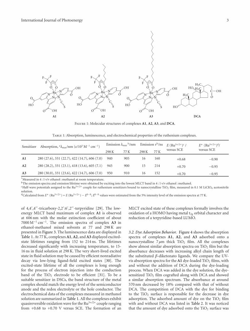
International Journal of Photoenergy 3
N
NN
O
O
O O
N
C
FF
F
S
ON
NN
O
O O
N
FF
F
N
NN
O
O O
N
FF
F
C
O
OH OH OHOH
OH
HO
HOHOHOHO
A1 A2 A3 DCA
−
H3C
H3CH3C
−−
Ru Ru Ru
O OC
SC
S
O O
OH OH
Figure 1: Molecular structures of complexes A1, A2, A3, and DCA.
Table 1: Absorption, luminescence, and electrochemical properties of the ruthenium complexes.
Sensitizer Absorption, aλmax/nm (ε/103 M−1 cm−1)Emission λmax
b/nm Emission τb/ns E (Ru3+/2+)c /versus SCE
E∗ (Ru3+/2+)d/versus SCE
298 K 77 K 298 K 77 K
A1 280 (27.6), 331 (22.7), 422 (14.7), 606 (7.0) 940 905 16 160 +0.68 −0.90
A2 280 (28.2), 331 (23.1), 418 (13.6), 605 (7.1) 945 900 15 214 +0.70 −0.95
A3 280 (30.0), 331 (23.6), 422 (14.7), 606 (7.0) 950 910 16 152 +0.70 −0.95aMeasured in 4 : 1 v/v ethanol : methanol at room temperature.
bThe emission spectra and emission lifetime were obtained by exciting into the lowest MLCT band in 4 : 1 v/v ethanol : methanol.cHalf-wave potentials assigned to the Ru3+/2+ couple for ruthenium sensitizers bound to nanocrystalline TiO2 film, measured in 0.1 M LiClO4 acetonitrilesolution.dCalculated from E∗ (Ru3+/2+) = E (Ru3+/2+) − E0−0; E0−0 values were estimated from the 5% intensity level of the emission spectra at 77 K.
of 4,4′,4′′-tricarboxy-2,2′:6′,2′′-terpyridine [29]. The low-energy MLCT band maximum of complex A1 is observedat 606 nm with the molar extinction coefficient of about7000 M−1 cm−1. The emission spectra of complex A3 inethanol-methanol mixed solvents at 77 and 298 K arepresented in Figure 3. The luminescence data are displayed inTable 1. At 77 K, complexes A1, A2, and A3 displayed excited-state lifetimes ranging from 152 to 214 ns. The lifetimesdecreased significantly with increasing temperature, to 15-16 ns in fluid solution at 298 K. The very short-lived excitedstate in fluid solution may be caused by efficient nonradiativedecay via low-lying ligand-field excited states [30]. Theexcited-state lifetime of all the complexes is long enoughfor the process of electron injection into the conductionband of the TiO2 electrode to be efficient [31]. To be asuitable sensitizer in DSCs, the band structure of the metalcomplex should match the energy level of the semiconductoranode and the redox electrolyte or the hole conductor. Theelectrochemical data of the complexes measured in methanolsolution are summarized in Table 1. All the complexes exhibitquasireversible oxidation wave for the Ru3+/2+ couple rangingfrom +0.68 to +0.70 V versus SCE. The formation of an
MLCT excited state of these complexes formally involves theoxidation of a HOMO having metal t2g orbital character andreduction of a terpyridine-based LUMO.
3.2. Dye Adsorption Behavior. Figure 4 shows the absorptionspectra of complexes A1, A2, and A3 adsorbed onto ananocrystalline 7 μm thick TiO2 film. All the complexesshow almost similar absorption spectra on TiO2 film but theabsorbance decreases with increasing alkyl chain length ofthe substituted β-diketonato ligands. We compare the UV-vis absorption spectra for the A1 dye-loaded TiO2 films, withand without the addition of DCA during the dye-loadingprocess. When DCA was added in the dye solution, the dye-sensitized TiO2 film cografted along with DCA and showeda similar absorption spectrum. The absorbance at around570 nm decreased by 18% compared with that of withoutDCA. The competition of DCA with the dye for bindingto the TiO2 surface is responsible for the decrease in dyeadsorption. The adsorbed amount of dye on the TiO2 filmwith and without DCA was listed in Table 2. It was noticedthat the amount of dye adsorbed onto the TiO2 surface was

4 International Journal of Photoenergy
Table 2: Adsorbed amount of dye and cell performancea of A1, A2, and A3 sensitizers with and without DCA.
Sensitizer DCA (mM) IPCEmax Jsc (mA cm−2) Voc (V) FF η (%) Dye loadb (10−8 mol cm−2)
A1 0 67 15.9 0.53 0.63 5.31 11.5
15 74 18.5 0.56 0.64 6.63 7.6
A2 0 69 17.2 0.57 0.63 6.18 9.4
15 72 18.1 0.58 0.65 6.82 7.2
A3 0 72 18.0 0.64 0.66 7.60 7.3
15 70 17.4 0.64 0.67 7.46 6.6aConditions: sealed cells; coadsorbate, DCA 0 or 15 mM; photoelectrode, TiO2 (20 μm thickness and 0.25 cm2); electrolyte, 0.6 M DMPII, 0.1 M LiI, 0.05 I2 in
AN; irradiated light, AM 1.5 solar light (100 mW cm−2). Jsc: short-circuit photocurrent density; Voc: open-circuit photovoltage; FF: fill factor; η: total powerconversion efficiency; IPCE: incident photon-to-current conversion efficiency.bSurface concentration of the dye molecules on TiO2 film.
0
5
10
15
Wavelength (nm)
/103
(M−1
cm−1
)
A1A2A3
350 450 550 650 750 850 950
Figure 2: UV-vis absorption spectra of complexes A1, A2, and A3in ethanol-methanol (4 : 1) solution.
reduced in the presence of DCA, as compared to that withoutDCA in the dye bath. For complex A1, the difference betweenthe amount of dye adsorbed onto the TiO2 surface in thepresence and absence of DCA in the dye bath is 34%. Thisis maybe due to the suppression of dye aggregation in thepresence of DCA. For complex A3, having long alkyl chainlength, the amount of dye adsorbed onto the TiO2 surface inthe absence of DCA decreases compared to that of A1. Therewas a small decrease in dye load when DCA was added intothe dye bath. The amount of complex A3 adsorbed onto theTiO2 surface decreased by only 9% in the presence of DCA,
0
1
Em
issi
onin
ten
sity
(a.u
.)×5
700 800 9000 1000 12001100
Wavelength (nm)
Figure 3: Emission spectra of complex A3 in ethanol-methanol(4 : 1) solution at 77 K (——) and 298 K (– – –).
whereas the complex A1 load was reduced about 34%. Thelong alkyl chain present on complex A3, may be suppress theaggregate formation onto the TiO2 surface and works likeDCA. It is suggested that A3 form an ordered dye layer onTiO2 surface and binds more strongly to the TiO2 surfacethan DCA.
3.3. Photovoltaic Properties. The photovoltaic performanceof complexes A1, A2, and A3 on nanocrystalline TiO2
electrode was studied under standard AM 1.5 irradia-tion (100 mW cm−2) using an electrolyte with a composi-tion of 0.6 M dimethylpropyl-imidazolium iodide (DMPII),0.05 M I2, and 0.1 M LiI in acetonitrile in the presenceand absence of DCA in the dye bath. The short-circuitphotocurrent density (Jsc), open-circuit voltage (Voc), fillfactors (FF), and overall cell efficiencies (η) for each dye-TiO2 electrode are summarized in Table 2. Figure 5 showsthe photocurrent action spectra for complexes A1 and A3 inthe presence and absence of DCA, where the incident photonto current conversion efficiency (IPCE) values is plotted asa function of wavelength. All complexes achieved efficientsensitization of nanocrystalline TiO2 over the whole visible

International Journal of Photoenergy 5
Wavelength (nm)400 500 600 700 800 900
0
0.2
0.4
0.6
0.8
1
Abs
orba
nce
(a.u
.)
A2-no DCAA1-no DCA A3-no DCA
A1-DCA
Figure 4: Absorption spectra of complexes A1, A2, and A3adsorbed onto a nanocrystalline 7 μm thick TiO2 film.
0
20
40
60
80
Wavelength (nm)
IPC
E(%
)
400 500 600 700 800 900
A1-no DCAA3-no DCA
A1-DCAA3-DCA
Figure 5: Photocurrent action spectra obtained with complexes A1and A3 with and without DCA addition during the sensitizationprocess. Incident photon-to-current conversion efficiency is plottedas a function of wavelength. A sandwich type sealed cell configura-tion was used to measure this spectrum. The electrolyte composi-tion was 0.6 M DMPII, 0.05 M I2, and 0.1 M LiI in acetonitrile.
range extending into the near IR region. The maximum IPCEvalues of complexes A1–A3 are given in Table 2.
As shown in Table 2, a solar cell containing complexA1 yielded a short-circuit photocurrent density (Jsc) of15.9 mA cm−2, an open-circuit photovoltage (Voc) of 0.53 V,and a fill factor (FF) of 0.63, corresponding to an overallconversion efficiency (η) of 5.3% in the absence of DCA. Theaddition of DCA gave a pronounced efficiency enhancementup to 6.6% with a short-circuit photocurrent density of18.5 mA cm−2 and an open-circuit photovoltage of 0.56 V.Although the amount of complex A1 adsorb on the TiO2 filmdecreased to 34% with the addition of DCA during the dye-loading process, the values of Jsc, Voc, and, thus, the efficiencywere increased as compared to the case without DCAaddition. As shown in Figure 5, complex A1 shows the IPCEvalue of 67% in the plateau region in the absence of DCA,and the maximum IPCE value increased up to 74% withthe addition of DCA during the dye-loading process. Theobserved changes in Jsc agreed well with the correspondingIPCE spectra for A1-sensitized DSCs with and without theaddition of DCA. The main possible explanation is that thecoadsorption of DCA prevents dye aggregation, which cancause intermolecular energy transfer and sequentially resultin the excited-state quenching of the dyes [19]. As a result, thereduction of dye load on the TiO2 surface in the presence ofDCA consequently results in more efficient electron injectionfrom the excited dyes to the TiO2 conduction band [19]. Amore efficient electron injection thus compensates for theless amount of dye adsorption.
It is interesting to find that A3-sensitized DSCs havinga long alkyl chain, in the absence of DCA, give a highoverall conversion efficiency of 7.6% with a short-circuitphotocurrent density of 18.0 mA cm−2 and an open-circuitphotovoltage of 0.64 V. The photovoltaic performance of A3-sensitized DSCs is higher than that of A3-sensitized DSCswith the addition of DCA during the dye-loading process.This indicates that the photovoltaic performance of bulkyalkyl chain substituted sensitizer A3 was not dependent onadditive DCA. It is expected that the injection of electroninto the TiO2 conduction band and the recombination ofelectrons in the TiO2 film with the oxidized species inthe redox electrolyte is unaffected in A3-sensitized DSCswith and without DCA addition. As shown in Table 2,the amount of adsorbed A3 on TiO2 surface with andwithout DCA addition is almost the same and also showssimilar photovoltaic performance which suggest a self-assembly property of complex A3 due to the presence ofa bulky alkyl chain substitute in the structure. A self-assembly property of the dye during the sensitization of TiO2
film is important to obtain efficient surface coverage andefficient electron injection and thus obtain high photovoltaicperformance of DSCs [19]. Figure 1 showed that the A3sensitizer contains long alkyl chain in the β-diketonatoligand which may produce surface blocking through sterichindrance, preventing the access of electrons to the redoxelectrolyte, which will be in favor of higher Voc. On theother hand, this bulky alkyl group may not only facilitatethe ordered molecular arrangement on the TiO2 surface butalso keep dye molecules at a distance, which may suppress

6 International Journal of Photoenergy
possibly intermolecular dye interaction, favoring higher Jsc
[19]. The protection by the alkyl chain is proven to be moreefficient as compared to the coadsorption of DCA underthe examined conditions. However, the less efficient surfaceprotection in A1 sensitizer resulted in poor photovoltaicperformance. In conclusion, higher power conversion effi-ciencies were obtained for DSCs based on A3 with bulkyalkyl substituent due to the inherent properties of the dyemolecule.
As illustrated in Figure 1, A2 sensitizer has an alkyl chainlength of C6 on the β-diketonato ligand which is shorter thanA3 sensitizer (C16). Thus, an expected intermediate perfor-mance for A2-sensitized DSCs was obtained in comparisonwith A1 and A3 under both conditions, with and without theDCA addition. From Table 2, it is clear that the dye load ofA2 dropped by about 23% due to the addition of DCA in thedye bath. However, the value of Jsc increased with decreasingdye coverage, probably due to the same reason as mentionedfor A1.
The A3 sensitizer having long alky chain substituent onthe β-diketonato ligand shows the best performance in thisseries. Thus, this class of diketonato ruthenium complexesserves as a basis for further design of new potential sensitizersby introducing suitable substituents on the diketonato ligandto prevent surface aggregation of the sensitizer for efficientinjection efficiencies and furthermore to enhance the molarextinction coefficient of the sensitizer.
4. Conclusions
Three panchromatic photosensitizers A1, A2, and A3 basedon 4,4′,4′′-tricarboxy-2,2′:6′,2′′-terpyridine-ruthenium(II)complexes with one β-diketonato chelating ligand con-taining different bulky alkyl chain lengths between C1–C16 were developed and systematically characterized usingelectrochemical and spectroscopic methods. The complexesachieved efficient sensitization of nanocrystalline TiO2
over the whole visible range extending into the nearIR region (ca. 950 nm). These dyes showed graduallyenhanced photovoltaic performance with increasing thealkyl chain length. The photovoltaic data of these newcomplexes show 7.6% power conversion efficiency understandard AM 1.5 irradiation (100 mW cm−2). To understandthe effect of the bulky substituent on the photovoltaicperformance of DSCs, we investigated the photovoltaicperformances of A1-, A2-, and A3-sensitized DSCs withand without DCA addition in the dye bath. We noticethat the photovoltaic performance of A3-sensitized DSCscontaining bulky alkyl chain length of C16 was independentof the DCA, while the A2 bearing alkyl chains length ofC6 and A1 without alkyl chain showed 10% and 24%,respectively, improvement in photovoltaic performance inthe presence of the DCA. Without DCA, A3-based DSCswere still superior to both A1 and A2 in the presence ofDCA. This is probably due to the inherently structuralnature of A3 molecule, functionalized with bulky alkylchain substituent, which resulted in excellent photovoltaicperformance.
References
[1] B. O’Regan and M. Gratzel, “A low-cost, high-efficiency solarcell based on dye-sensitized colloidal TiO2 films,” Nature, vol.353, no. 6346, pp. 737–740, 1991.
[2] A. Hagfeld and M. Gratzel, “Light-induced redox reactions innanocrystalline systems,” Chemical Reviews, vol. 95, no. 1, pp.49–68, 1995.
[3] A. Hagfeldt and M. Gratzel, “Molecular photovoltaics,”Accounts of Chemical Research, vol. 33, no. 5, pp. 269–277,2000.
[4] M. Gratzel, “Solar energy conversion by dye-sensitized photo-voltaic cells,” Inorganic Chemistry, vol. 44, no. 20, pp. 6841–6851, 2005.
[5] M. Gratzel, “Conversion of sunlight to electric power bynanocrystalline dye-sensitized solar cells,” Journal of Photo-chemistry and Photobiology A, vol. 164, no. 1–3, pp. 3–14, 2004.
[6] A. Mishra, M. K. R. Fischer, and P. Buuerle, “Metal-Freeorganic dyes for dye-Sensitized solar cells: from structure:property relationships to design rules,” Angewandte Chemie,vol. 48, no. 14, pp. 2474–2499, 2009.
[7] A. Islam, H. Sugihara, and H. Arakawa, “Molecular designof ruthenium(II) polypyridyl photosensitizers for efficientnanocrystalline TiO2 solar cells,” Journal of Photochemistry andPhotobiology A, vol. 158, no. 2-3, pp. 131–138, 2003.
[8] A. Hagfeldt, G. Boschloo, L. Sun, L. Kloo, and H. Pettersson,“Dye-sensitized solar cells,” Chemical Reviews, vol. 110, no. 11,pp. 6595–6663, 2010.
[9] T. Funaki, M. Yanagida, N. Onozawa-Komatsuzaki, K. Kasuga,Y. Kawanishi, and H. Sugihara, “Efficient panchromaticsensitization of nanocrystalline TiO2 -based solar cells using2-pyridinecarboxylate-substituted Ruthenium(II) complexes,”Chemistry Letters, vol. 38, no. 1, pp. 62–63, 2009.
[10] A. Islam, F. A. Chowdhury, Y. Chiba et al., “Synthesisand characterization of new efficient tricarboxyterpyridyl (β-diketonato) ruthenium(II) sensitizers and their applications indye-sensitized solar cells,” Chemistry of Materials, vol. 18, no.22, pp. 5178–5185, 2006.
[11] M. K. Nazeeruddin, P. Pechy, T. Renouard et al., “Engineeringof efficient panchromatic sensitizers for nanocrystalline TiO2-based solar cells,” Journal of the American Chemical Society, vol.123, no. 8, pp. 1613–1624, 2001.
[12] A. Islam, F. A. Chowdhury, Y. Chiba et al., “Ruthenium(II)tricarboxyterpyridyl complex with a fluorine-substituted β-diketonato ligand for highly efficient dye-sensitized solarcells,” Chemistry Letters, vol. 34, no. 3, pp. 344–345,2005.
[13] Y. Chiba, A. Islam, Y. Watanabe, R. Komiya, N. Koide, and L.Han, “Dye-sensitized solar cells with conversion efficiency of11.1%,” Japanese Journal of Applied Physics, Part 2, vol. 45, no.24–28, pp. L638–L640, 2006.
[14] Q. Wang, S. Ito, M. Gratzel et al., “Characteristics of high effi-ciency dye-sensitized solar cells,” Journal of Physical ChemistryB, vol. 110, no. 50, pp. 25210–25221, 2006.
[15] A. Islam, H. Sugihara, M. Yanagida et al., “Efficient panchro-matic sensitization of nanocrystalline TiO2 films by β-diketonato ruthenium polypyridyl complexes,” New Journal ofChemistry, vol. 26, no. 8, pp. 966–968, 2002.
[16] S. Gao, A. Islam, Y. Numata, and L. Han, “A β-diketonatoruthenium(II) complex with high molar extinction coefficientfor panchromatic sensitization of nanocrystalline TiO2 film,”Applied Physics Express, vol. 3, no. 6, Article ID 062301,2010.

International Journal of Photoenergy 7
[17] A. Morandeira, I. Lopez-Duarte, B. O’Regan et al., “Ru(II)-phthalocyanine sensitized solar cells: the influence of co-adsorbents upon interfacial electron transfer kinetics,” Journalof Materials Chemistry, vol. 19, no. 28, pp. 5016–5026, 2009.
[18] Z. Zhang, N. Evans, S. M. Zakeeruddin, R. Humphry-Baker, and M. Gratzel, “Effects of ω-guanidinoalkyl acids ascoadsorbents in dye-sensitized solar cells,” Journal of PhysicalChemistry C, vol. 111, no. 1, pp. 398–403, 2007.
[19] X. Jiang, T. Marinado, E. Gabrielsson, D. P. Hagberg, L. Sun,and A. Hagfeldt, “Structural Modification of organic dyes forefficient coadsorbent-free dye-sensitized solar cells,” Journal ofPhysical Chemistry C, vol. 114, no. 6, pp. 2799–2805, 2010.
[20] H. Chen, H. Huang, X. Huang et al., “High molar extinc-tion coefficient branchlike organic dyes containing Di(p-tolyl)phenylamine donor for dye-sensitized solar cells appli-cations,” Journal of Physical Chemistry C, vol. 114, no. 7, pp.3280–3286, 2010.
[21] X. Ren, Q. Feng, G. Zhou, C. H. Huang, and Z. S. Wang,“Effect of cations in coadsorbate on charge recombination andconduction band edge movement in dye-sensitized solar cells,”Journal of Physical Chemistry C, vol. 114, no. 15, pp. 7190–7195, 2010.
[22] T. Marinado, M. Hahlin, X. Jiang et al., “Surface molecularquantification and photoelectrochemical characterization ofmixed organic dye and coadsorbent layers on TiO2 for dye-sensitized solar cells,” Journal of Physical Chemistry C, vol. 114,no. 27, pp. 11903–11910, 2010.
[23] J. H. Yum, S. J. Moon, R. Humphry-Baker et al., “Effect ofcoadsorbent on the photovoltaic performance of squarainesensitized nanocrystalline solar cells,” Nanotechnology, vol. 19,no. 42, Article ID 424005, 2008.
[24] S. Ito, H. Miura, S. Uchida et al., “High-conversion-efficiencyorganic dye-sensitized solar cells with a novel indoline dye,”Chemical Communications, no. 41, pp. 5194–5196, 2008.
[25] C. Kim, H. Choi, S. Kim et al., “Molecular engineering oforganic sensitizers containing p-phenylene vinylene unit fordye-sensitized solar cells,” Journal of Organic Chemistry, vol.73, no. 18, pp. 7072–7079, 2008.
[26] H. Choi, S. Kim, S. O. Kang et al., “Stepwise cosensitizationof nanocrystalline TiO2 films utilizing Al2O3 layers in dye-sensitized solar cells,” Angewandte Chemie, vol. 47, no. 43, pp.8259–8263, 2008.
[27] N. Koumura, Z. S. Wang, S. Mori, M. Miyashita, E. Suzuki,and K. Hara, “Alkyl-functionalized organic dyes for efficientmolecular photovoltaics,” Journal of the American ChemicalSociety, vol. 128, no. 44, pp. 14256–14257, 2006.
[28] J. C. Sloop, C. L. Bumgardner, and W. D. Loehle, “Synthesis offluorinated heterocycles,” Journal of Fluorine Chemistry, vol.118, no. 1-2, pp. 135–147, 2002.
[29] A. Mamo, A. Juris, G. Calogero, and S. Campagna, “Near-infrared luminescence at room temperature of two newosmium(II) terdentate polypyridine complexes,” ChemicalCommunications, no. 10, pp. 1225–1226, 1996.
[30] A. Islam, N. Ikeda, A. Yoshimura, and T. Ohno, “Nonra-diative transition of phosphorescent charge-transfer statesof ruthenium(II)-to-2,2′-biquinoline and ruthenium(II)-to-2,2′:6′,2
′′-terpyridine in the solid state,” Inorganic Chemistry,
vol. 37, no. 12, pp. 3093–3098, 1998.[31] Y. Tachibana, S. A. Haque, I. P. Mercer, J. R. Durrant, and D. R.
Klug, “Electron injection and recombination in dye sensitizednanocrystalline titanium dioxide films: a comparison ofruthenium bipyridyl and porphyrin sensitizer dyes,” Journalof Physical Chemistry B, vol. 104, no. 6, pp. 1198–1205, 2000.
Hindawi Publishing CorporationInternational Journal of PhotoenergyVolume 2011, Article ID 617439, 4 pagesdoi:10.1155/2011/617439
Research Article
Metal-Free Counter Electrode for Efficient Dye-SensitizedSolar Cells through High Surface Area and Large Porous Carbon
Pavuluri Srinivasu,1 Surya Prakash Singh,2 Ashraful Islam,2, 3 and Liyuan Han2
1 International Center for Young Scientists, International Center for Materials Nanoarchitectonics,National Institute for Materials Science, 1-1 Namiki, Tsukuba, Ibaraki 305-0044, Japan
2 Advanced Photovoltaics Center, National Institute for Materials Science,1-2-1 Sengen, Tsukuba, Ibaraki 305-0047, Japan
3 Center of Excellence for Research in Engineering, Materials (CEREM), College of Engineering, King Saud University,Riyadh 11421, Saudi Arabia
Correspondence should be addressed to Pavuluri Srinivasu, [email protected]
Received 10 March 2011; Accepted 8 May 2011
Academic Editor: Mohamed Sabry Abdel-Mottaleb
Copyright © 2011 Pavuluri Srinivasu et al. This is an open access article distributed under the Creative Commons AttributionLicense, which permits unrestricted use, distribution, and reproduction in any medium, provided the original work is properlycited.
Highly efficient, large mesoporous carbon is fabricated as a metal-free counter electrode for dye-sensitized solar cells. Themesoporous carbon shows very high energy conversion efficiency of 7.1% compared with activated carbon. The mesoporouscarbon is prepared and characterized by nitrogen adsorption, scanning electron microscopy (SEM), and transmission electronmicroscopy (TEM). The nitrogen adsorption data reveals that the material possesses BET specific surface area ca.1300 m2/g andpore diameter 4.4 nm. Hexagonal rod-like morphology and ordered pore structure of mesoporous carbon are confirmed byelectron microscopy data. The better performance of this carbon material is greatly benefited from its ordered interconnectedmesoporous structure and high surface area.
1. Introduction
Global energy demand is likely to increase with the expansionof economy, even though great efforts are made to increasethe energy utilization efficiency. In recent years, fuel cells andsolar cells have contributed remarkably for the developmentof renewable energy technologies. Photovoltaic cells suchas dye-sensitized solar cells (DSCs) have attracted muchattention as an alternative energy source for future require-ments [1], which composed of porous nanostructured oxidefilm with adsorbed dye molecules as a dye-sensitized anode,an electrolyte containing iodide/triiodide redox couple,and a platinized fluorine-doped tin oxide (FTO) glass asthe counter electrode [2–4]. DSCs have advantages overtraditional Si-solar cells due to low cost, easy fabrication,and high energy conversion efficiency [5, 6]. For additionalimprovement in energy efficiency and commercialization ofDSCs [7, 8], further cost reduction is necessary. Therefore,efforts have been made to lower the production cost of DSCs
by using flexible ITO-coated polyester film, metal foil [9],and organic dyes or metalorganic complex dyes [10]. InDSCs the platinum counter electrode is very crucial towardscatalytic reduction of tri-iodine. But the platinum is anexpensive metal and takes large portion of fabrication costof DSCs, which retards commercialization of the process.To reduce to the cost of DSCs process various carbonmaterials such as carbon black [11], activated carbon [12],carbon nanotubes, porous carbon [13], and graphite [14]have been investigated as counter electrode. However, energyconversion efficiency of reported carbon counter electrodeof DSCs is still low. Therefore, further enhancement ofefficiency is necessary. Among the other carbon materials,mesoporous carbon materials have received much attentiondue to their large internal surface area and pore volume,tunable and narrow pore diameter [15, 16]. Templatedsynthesis method of mesoporous carbon, which is alsoknown as “nanocasting” has been extensively used due tothe obtained material possesses uniform and interconnected
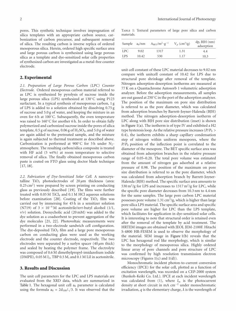
2 International Journal of Photoenergy
pores. This synthetic technique involves impregnation ofsilica templates with an appropriate carbon source, car-bonization of carbon precursor, and subsequent removalof silica. The resulting carbon is inverse replica of orderedmesoporous silica. Herein, ordered high specific surface areaand large porous carbon is synthesized using large poroussilica as a template and dye-sensitized solar cells propertiesof synthesized carbon are investigated as a metal-free counterelectrode.
2. Experimental
2.1. Preparation of Large Porous Carbon (LPC) CounterElectrode. Ordered mesoporous carbon material referred toas LPC is synthesized by pyrolysis of sucrose inside thelarge porous silica (LPS) synthesized at 130◦C using P123surfactant. In a typical synthesis of mesoporous carbon, 1 gof LPS is added to a solution obtained by dissolving 0.75 gof sucrose and 5.0 g of water, and keeping the mixture in anoven for 6 h at 100◦C. Subsequently, the oven temperaturewas raised to 160◦C for another 6 h. In order to obtain fullypolymerized and carbonized sucrose inside the pores of silicatemplate, 0.5 g of sucrose, 0.06 g of H2SO4, and 5.0 g of waterare again added to the pretreated sample, and the mixtureis again subjected to thermal treatment as described above.Carbonization is performed at 900◦C for 5 h under N2-atmosphere. The resulting carbon/silica composite is treatedwith HF acid (5 wt%) at room temperature to selectiveremoval of silica. The finally obtained mesoporous carbonpaste is coated on FTO glass using doctor blade technique[17, 18].
2.2. Fabrication of Dye-Sensitized Solar Cell. A nanocrys-talline TiO2 photoelectrodes of 20 μm thickness (area:0.25 cm2) were prepared by screen printing on conductingglass as previously described [19]. The films were furthertreated with 0.05 M TiCl4 and 0.1 M HCl aqueous solutionsbefore examination [20]. Coating of the TiO2 film wascarried out by immersing for 45 h in a sensitizer solution(N719) of 3 × 10⁻⁴ M acetonitrile/tert-butyl alcohol (1/1,v/v) solution. Deoxycholic acid (20 mM) was added to thedye solution as a coadsorbent to prevent aggregation of thedye molecules [21, 22]. Photovoltaic measurements wereperformed in a two-electrode sandwich cell configuration.The dye-deposited TiO2 film and a large pore mesoporouscarbon on conducting glass were used as the workingelectrode and the counter electrode, respectively. The twoelectrodes were separated by a surlyn spacer (40 μm thick)and sealed by heating the polymer frame. The electrolytewas composed of 0.6 M dimethylpropyl-imidazolium iodide(DMPII), 0.05 M I2, TBP 0.5 M, and 0.1 M LiI in acetonitrile.
3. Results and Discussion
The unit cell parameters for the LPC and LPS materials areevaluated from the XRD data, which are summarized inTable 1. The hexagonal unit cell a0 parameter is calculatedusing the formula a0 = 2d100/
√3. It was observed that the
Table 1: Textural parameters of large pore silica and carbonmaterials.
Sample a0/nm ABET/m2·g−1 Vp (cm3/g) dp, BJH (nm)adsorption
LPC 9.02 1317 1.31 4.4
LPS 10.42 530 1.17 10.3
unit cell constant of these LPC material decreases to 9.02 nmcompare with unitcell constant of 10.42 for LPS due tostructural pore shrinkage after removal of the template.Nitrogen adsorption-desorption isotherms are measured at77 K on a Quantachrome Autosorb 1 volumetric adsorptionanalyzer. Before the adsorption measurements, all samplesare out gassed at 250◦C in the port of the adsorption analyzer.The position of the maximum on pore size distributionis referred to as the pore diameter, which was calculatedfrom adsorption branches by Barrett-Joyner-Halenda (BJH)method. The nitrogen adsorption-desorption isotherm ofLPC along with BJH pore size distribution (inset) is shownin Figure 1(a). The isotherm is of type IV and exhibited a H2type hysteresis loop. As the relative pressure increases (P/P0 >0.4), the isotherm exhibits a sharp capillary condensationstep of nitrogen within uniform mesopores, where theP/P0 position of the inflection point is correlated to thediameter of the mesopore. The BET specific surface area wasobtained from adsorption branches in the relative pressurerange of 0.05–0.20. The total pore volume was estimatedfrom the amount of nitrogen gas adsorbed at a relativepressure of 0.98. The position of the maximum on poresize distribution is referred to as the pore diameter, whichwas calculated from adsorption branch by Barrett-Joyner-Halenda (BJH) method. The specific surface area amounts to530 m2/g for LPS and increases to 1317 m2/g for LPC, whilethe specific pore diameter decreases from 10.3 nm to 4.4 nmfor the same samples. The large pore carbon LPC materialpossesses pore volume 1.31 cm3/g, which is higher than largepore silica LPS material. The specific surface area and specificpore volume are higher for LPC than the LPS template,which facilitates for application in dye-sensitized solar cells.It is interesting to note that structural order is retained evenafter the removal of the template by acid treatment. TheHRTEM images are obtained with JEOL JEM-2100F. HitachiS-4800 HR-FESEM is used to observe the morphology ofthe material. SEM image in Figure 1(b) reveals that theLPC has hexagonal rod like morphology, which is similarto the morphology of mesoporous silica. Highly orderedlinear array of pore channels and pore structure of LPCwas confirmed by high resolution transmission electronmicroscopy (Figures 1(c) and 1(d)).
Monochromatic incident photon-to-current conversionefficiency (IPCE) for the solar cell, plotted as a function ofexcitation wavelength, was recorded on a CEP-2000 system(Bunkoh-Keiki Co. Ltd.). IPCE at each incident wavelengthwas calculated from (1), where Isc is the photocurrentdensity at short circuit in mA cm−2 under monochromaticirradiation, q is the elementary charge, λ is the wavelength of

International Journal of Photoenergy 3
Pore diameter (nm)
0 0.2 0.4 0.6 0.8 1200
400
600
800
1000
Relative ressure P/P0p
2 4 6 8 10 120
0.1
0.2
0.3
0.4
0.5
0.6A
mou
nt
adso
rbed
(cm
3·g−1
)
Dv(d
)(c
m3·(g·n
m)−
1)
(a)
5μm
(b)
20 nm
(c)
50 nm
(d)
Figure 1: (a) Nitrogen adsorption isotherm (• adsorption, ◦ desorption) and BJH pore-size distribution (in set) of LPC material. (b) SEMimage of LPC material. (c, d) TEM images of LPC.
incident radiation in nm, and P0 is the incident radiative fluxin Wm−2
IPCE(λ) = 1240
(ISC
qλP0
). (1)
The photocurrent density-voltage curves and incidentphoton-to-current efficiency (IPCE) spectra of the cells arebased on N719 dye under the illumination of air mass (AM)1.5 sunlight (100 mW/cm2, WXS-155S-10: Wacom DensoCo. Japan).
Photovoltaic performances of DSCs based on the meso-porous carbon and activated charcoal are shown in Figure 2.The short circuit current (Jsc), the open-circuit voltage (Voc),the fill factor (FF), and the overall conversion efficiency (η)are summarized in Table 2. The results indicate that theactivated charcoal shows poor performance compare withmesoporous carbon. The LPC counter electrode shows Jsc of12.07 mA/cm2, Voc of 0.80 V and FF of 0.66% superior overJsc of 12.07 mA/cm2, and Voc of 0.76 V and FF of 0.15% ofactivated charcoal material. The overall conversion efficiency
Table 2: Photovoltaic parameters of DSCs based on mesoporouscarbon and activated carbon electrodes.
Sample Jsc/mA cm−2 Voc/V FF% η/%
LPC 13.41 0.80 0.66 7.1
AC 12.07 0.76 0.15 1.4
achieved is 7.1% and 1.44% for LPC and AC, respectively.The higher FF and η indicate that LPC is more efficient thanAC material.
4. Conclusions
High surface area and large mesoporous carbon LPC withordered pore structure has been explored as the metal-freecounter electrode for DSCs. Nitrogen adsorption isothermmeasurement indicates that LPC material shows very highsurface area and large pore volume than mesoporous silicaLPS material. SEM and TEM analyses confirm that LPCmaterial retain morphology and order pore structure of
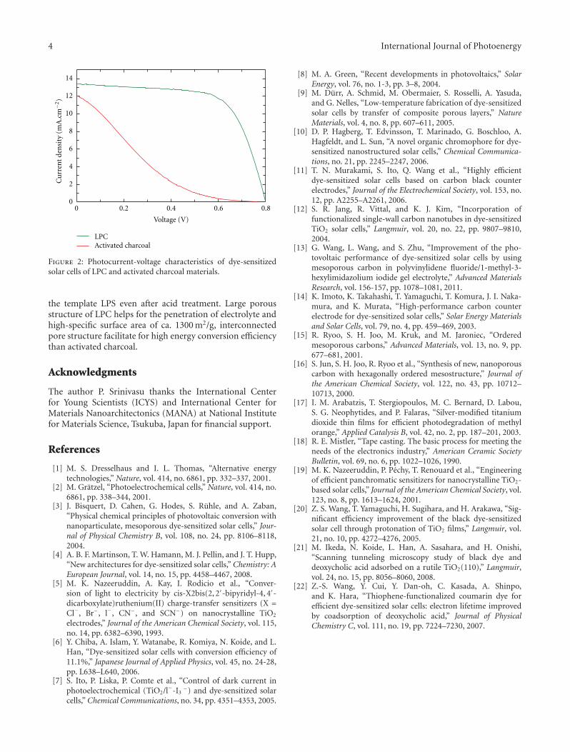
4 International Journal of Photoenergy
Voltage (V)
0 0.2 0.4 0.6 0.8
Cu
rren
tde
nsi
ty(m
A.c
m−2
0
2
4
6
8
10
12
14
LPCActivated charcoal
)
Figure 2: Photocurrent-voltage characteristics of dye-sensitizedsolar cells of LPC and activated charcoal materials.
the template LPS even after acid treatment. Large porousstructure of LPC helps for the penetration of electrolyte andhigh-specific surface area of ca. 1300 m2/g, interconnectedpore structure facilitate for high energy conversion efficiencythan activated charcoal.
Acknowledgments
The author P. Srinivasu thanks the International Centerfor Young Scientists (ICYS) and International Center forMaterials Nanoarchitectonics (MANA) at National Institutefor Materials Science, Tsukuba, Japan for financial support.
References
[1] M. S. Dresselhaus and I. L. Thomas, “Alternative energytechnologies,” Nature, vol. 414, no. 6861, pp. 332–337, 2001.
[2] M. Gratzel, “Photoelectrochemical cells,” Nature, vol. 414, no.6861, pp. 338–344, 2001.
[3] J. Bisquert, D. Cahen, G. Hodes, S. Ruhle, and A. Zaban,“Physical chemical principles of photovoltaic conversion withnanoparticulate, mesoporous dye-sensitized solar cells,” Jour-nal of Physical Chemistry B, vol. 108, no. 24, pp. 8106–8118,2004.
[4] A. B. F. Martinson, T. W. Hamann, M. J. Pellin, and J. T. Hupp,“New architectures for dye-sensitized solar cells,” Chemistry: AEuropean Journal, vol. 14, no. 15, pp. 4458–4467, 2008.
[5] M. K. Nazeeruddin, A. Kay, I. Rodicio et al., “Conver-sion of light to electricity by cis-X2bis(2, 2′-bipyridyl-4, 4′-dicarboxylate)ruthenium(II) charge-transfer sensitizers (X =Cl−, Br−, l−, CN−, and SCN−) on nanocrystalline TiO2
electrodes,” Journal of the American Chemical Society, vol. 115,no. 14, pp. 6382–6390, 1993.
[6] Y. Chiba, A. Islam, Y. Watanabe, R. Komiya, N. Koide, and L.Han, “Dye-sensitized solar cells with conversion efficiency of11.1%,” Japanese Journal of Applied Physics, vol. 45, no. 24-28,pp. L638–L640, 2006.
[7] S. Ito, P. Liska, P. Comte et al., “Control of dark current inphotoelectrochemical (TiO2/l−-I3
−) and dye-sensitized solarcells,” Chemical Communications, no. 34, pp. 4351–4353, 2005.
[8] M. A. Green, “Recent developments in photovoltaics,” SolarEnergy, vol. 76, no. 1-3, pp. 3–8, 2004.
[9] M. Durr, A. Schmid, M. Obermaier, S. Rosselli, A. Yasuda,and G. Nelles, “Low-temperature fabrication of dye-sensitizedsolar cells by transfer of composite porous layers,” NatureMaterials, vol. 4, no. 8, pp. 607–611, 2005.
[10] D. P. Hagberg, T. Edvinsson, T. Marinado, G. Boschloo, A.Hagfeldt, and L. Sun, “A novel organic chromophore for dye-sensitized nanostructured solar cells,” Chemical Communica-tions, no. 21, pp. 2245–2247, 2006.
[11] T. N. Murakami, S. Ito, Q. Wang et al., “Highly efficientdye-sensitized solar cells based on carbon black counterelectrodes,” Journal of the Electrochemical Society, vol. 153, no.12, pp. A2255–A2261, 2006.
[12] S. R. Jang, R. Vittal, and K. J. Kim, “Incorporation offunctionalized single-wall carbon nanotubes in dye-sensitizedTiO2 solar cells,” Langmuir, vol. 20, no. 22, pp. 9807–9810,2004.
[13] G. Wang, L. Wang, and S. Zhu, “Improvement of the pho-tovoltaic performance of dye-sensitized solar cells by usingmesoporous carbon in polyvinylidene fluoride/1-methyl-3-hexylimidazolium iodide gel electrolyte,” Advanced MaterialsResearch, vol. 156-157, pp. 1078–1081, 2011.
[14] K. Imoto, K. Takahashi, T. Yamaguchi, T. Komura, J. I. Naka-mura, and K. Murata, “High-performance carbon counterelectrode for dye-sensitized solar cells,” Solar Energy Materialsand Solar Cells, vol. 79, no. 4, pp. 459–469, 2003.
[15] R. Ryoo, S. H. Joo, M. Kruk, and M. Jaroniec, “Orderedmesoporous carbons,” Advanced Materials, vol. 13, no. 9, pp.677–681, 2001.
[16] S. Jun, S. H. Joo, R. Ryoo et al., “Synthesis of new, nanoporouscarbon with hexagonally ordered mesostructure,” Journal ofthe American Chemical Society, vol. 122, no. 43, pp. 10712–10713, 2000.
[17] I. M. Arabatzis, T. Stergiopoulos, M. C. Bernard, D. Labou,S. G. Neophytides, and P. Falaras, “Silver-modified titaniumdioxide thin films for efficient photodegradation of methylorange,” Applied Catalysis B, vol. 42, no. 2, pp. 187–201, 2003.
[18] R. E. Mistler, “Tape casting. The basic process for meeting theneeds of the electronics industry,” American Ceramic SocietyBulletin, vol. 69, no. 6, pp. 1022–1026, 1990.
[19] M. K. Nazeeruddin, P. Pechy, T. Renouard et al., “Engineeringof efficient panchromatic sensitizers for nanocrystalline TiO2-based solar cells,” Journal of the American Chemical Society, vol.123, no. 8, pp. 1613–1624, 2001.
[20] Z. S. Wang, T. Yamaguchi, H. Sugihara, and H. Arakawa, “Sig-nificant efficiency improvement of the black dye-sensitizedsolar cell through protonation of TiO2 films,” Langmuir, vol.21, no. 10, pp. 4272–4276, 2005.
[21] M. Ikeda, N. Koide, L. Han, A. Sasahara, and H. Onishi,“Scanning tunneling microscopy study of black dye anddeoxycholic acid adsorbed on a rutile TiO2(110),” Langmuir,vol. 24, no. 15, pp. 8056–8060, 2008.
[22] Z.-S. Wang, Y. Cui, Y. Dan-oh, C. Kasada, A. Shinpo,and K. Hara, “Thiophene-functionalized coumarin dye forefficient dye-sensitized solar cells: electron lifetime improvedby coadsorption of deoxycholic acid,” Journal of PhysicalChemistry C, vol. 111, no. 19, pp. 7224–7230, 2007.
Hindawi Publishing CorporationInternational Journal of PhotoenergyVolume 2011, Article ID 869589, 9 pagesdoi:10.1155/2011/869589
Research Article
Conversion of Dagang Vacuum Residue into Oxygen-ContainingOrganic Compounds by Photo-Oxidation with H2O2 over TiO2
Heng-Shen Xie,1, 2 Zhi-Min Zong,1 Qing Wei,1 Tong Liu,1 Jian-Jun Zhao,1 Pei-Zhi Zhao,1
Shi-Hua Zhang,1 and Xian-Yong Wei1, 3
1 Key Laboratory of Coal Processing and Efficient Utilization (Ministry of Education),China University of Mining and Technology, Xuzhou, Jiangsu 221008, China
2 Division of Science & Technology, Xuzhou Institute of Architectural Technology, Xuzhou, Jiangsu 221116, China3 Hubei Coal Conversion and New Carbon Materials Key Laboratory, Wuhan University of Science and Technology,Wuhan, Hubei 430081, China
Correspondence should be addressed to Xian-Yong Wei, wei [email protected]
Received 26 October 2010; Revised 19 January 2011; Accepted 21 April 2011
Academic Editor: J. Anthony Byrne
Copyright © 2011 Heng-Shen Xie et al. This is an open access article distributed under the Creative Commons Attribution License,which permits unrestricted use, distribution, and reproduction in any medium, provided the original work is properly cited.
The photocatalytic depolymerization of Dagang vacuum residue (DVR) was carried out with H2O2 over TiO2 in a photochemicalreactor. Most of the organic matter in DVR was converted into oxygen-containing organic compounds. The yields of carboxylicacids, oxalates, epoxy compounds, and hydroxyl compounds from DVR oxidation are 40.6%, 36.4%, 17.86%, and 13.5%,respectively. In addition, the oxidation causes significant decrease in viscosity and chromaticity of DVR. The related reactionmechanisms are discussed according to the experimental results.
1. Introduction
Heavy oil becomes more and more important with rapidreduction of light oil and drastic increase of liquid fuels [1–5]. As typical heavy oil in China, Dagang vacuum residue(DVR) has high viscosity and chromaticity [6].
Photo-catalytic oxidation (PCO) has been widely appliedto many aspects such as solar energy transformation,environmental protection and the syntheses of coating,cosmetic and printing ink, food-packaging materials, gassensors and functional ceramics [7–15]. Almost all theorganic matter (OM) in aqueous solution can be convertedinto carbon dioxide and water by PCO; hydroxyl oxidationand electron-hole pair oxidation are principal processes inthe course of oxidation [16–18]. However, selective PCOof heavy oil in organic solvent has not been reported toour knowledge. In the present study, we found that OMin DVR can be converted into oxygen-containing organiccompounds (OCOCs), which can be used as industrialraw materials for the synthesis of dyes and medicines.Particularly, dialkyl oxalates in the OCOCs are reactiveintermediates for preparing chemical cold light source [19–22].
2. Experimental Section
2.1. Samples and Reagents. DVR, the residue of crude oilvacuum distillated later and collected from Dagang OilField, Tianjin Municipality, China, was preserved in sealedcondition. Table 1 shows the elementary properties andultimate analysis of DVR. Cyclohexane, acetone, and hydro-gen peroxide (30% wt) are commercial purchased analyticalreagents, and all organic solvents used in the experimentwere distilled prior to use. Titanium dioxide as photocatalystwas prepared by Sol-Gel method and characterized byultraviolet visible (UV-VIS), X-ray diffraction (XRD), andtransmission electron microscopy (TEM) (as shown inFigures SI-1, 2, 3, and 4 and Table SI-1, see SupplementaryMaterials available at doi:10.1155/2011/869589), implyingthe homemade powders are anatase nanometer particles, andits particle radius is no more than 20 nm, and its propertiesare similar to the commercial reagent P-25 [23].
2.2. Instruments and Equipment. The SGY-1 multifunctionsphotochemistry reactor with the function of rotating andwith 500 W low-pressure mercury lamp as light source,which can emit around 85% ultraviolet light with wavelength

2 International Journal of Photoenergy
Information on the compositionand structure of DVR
Renew
Catalyst
Ultrasonic scattered for 10 min
Reaction mixture
Ultraviolet radiation for 13 h by filtration
Solid phaseLiquid phase
Water phase CSFODVR
COD analysesFTIR andGC/MS analysis
Information on the compositionand structure of ODVR
Eluted with acetoneexhaustively
ASFODVR
GC/MS analyses
FTIR and GC/MS analysis
Calcinedactivation
Insoluble fractions
0.5 mL H2O2,0.01 g TiO2
0.005 g DVR, 10 mL cyclohexane(CSFDVR)
Separation by separatoryfunnel
Figure 1: Procedure for DVR oxidation, subsequent treatment, and products analysis.
of 365 nm (its energy distribution as shown in Table SI-8), was made in Nanjing Sidongke Electric Equipment Co.of China. The reactor was used to study the quantumyield of photochemistry reaction, especially the synthesisof new materials or the degradation of organic contami-nations (as Figure SI-7). The instruments for analyses ofproducts are a Nicolet Magna IR-560 Fourier transforminfrared (FTIR) and a Hewlett-Packard 6890/5973 gas chro-matography/mass spectrometer (GC/MS) equipped with acapillary column coated with HP-5 (cross-link 5% PH MEsiloxane, 30 m × 0.25 mm i.d., 0.25 μm film thickness) and aquadrupole analyzer and operated in electron impact (70 eV)mode.
2.3. Photochemical Treatment and Analyses Method. Asshown in Figure 1, 0.005 g of DVR was dissolved in 10 mLcyclohexane and mixed with TiO2 (amount of 0.01 g) andH2O2 (ca. 0.5 mL). The mixtures were dispersed underultrasonic for 10 min and illuminated with 500 watt low-pressure ultraviolet mercury lamp for 13 hours in electro-magnetic stirring. Then the reaction mixture was filteredand separated and eluted with cyclohexane and acetone,respectively. The cyclohexane-soluble fraction (CSFODVR)and the acetone-soluble fraction (ASFODVR) were analyzedwith GC-MS or FTIR. The residue was calcined to obtainthe service life of catalyst. The chemical oxygen demand(COD) of the aqueous soluble was determined using titrationwith potassium dichromate. In addition to the modelcompounds such as liquid paraffin, decahydronaphthene andtetrahydronaphthalene were oxidized by UV light to analyzethe depolymerization mechanism of DVR photo-catalyticoxidation under the same condition. The reaction results ofmodel compounds were shown in Tables SI 3, 4 and 5. Andthe reaction results of DVR were also discussed with FTIRanalyses.
3. Results and Discussion
3.1. Analysis of Cyclohexane Photo-Oxidation. Different sol-vents have different polarity and stability, especially whenthey are illuminated by UV light. DVR mainly consists oflow-polarity alkyl saturated hydrocarbon. Hence, cyclohex-ane with lower polarity and stability to UV light is selectedas solvent in PCO according to similar dissolve mutuallytheory. Of course, the products from the PCO of cyclohexanemay have effect on the analysis result of ODVR. So inorder to eliminate the interference, the cyclohexane wasoxidized alone by photo-catalytic oxidation and with GC/MSanalyses. The result is exhibited in Figure 2, the oxidationproducts are listed in Table SI-2. As shown Figure 2,in total six products were identified, including cyclohex-anol, cyclohexanone, cyclohexyl formate, cyclohexylcyclo-hexane, (cyclohexyloxy)cyclohexane, and cyclohexyl hex-anoate. Among the oxidation products the relative contentsof compound 6 ((cyclohexyloxy)cyclohexane) and com-pound 2 (cyclohexanol) are higher and account for 14.30%and 5.76%, respectively. However, no 1-cyclohexylcyclohex-1-ene, cyclohexene, and cyclohexy-lidenecyclohexane weredetected, implying active hydrogens in cyclohexane ringcan be substituted partly by hydroxyl radicals to formcyclohexane derivatives, but the derivatives are difficult toeliminate and to form the products of cyclohexane ringopening or unsaturated compounds. The mechanism ofproduct formation is represented in Scheme 1. Where thesolvent is not oxidized under the mild conditions, presentselection of solvent is more appropriate.
3.2. Effect of TiO2 on DVR Oxidation by FTIR Analysis. Asshown in Figure 3, no absorbance at 3480 cm−1 was observedin EI (the system of DVR cyclohexane solution) and EII
(the system of DVR cyclohexane solution oxidized with
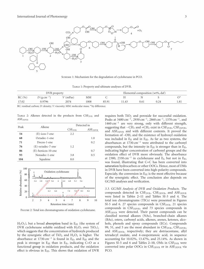
International Journal of Photoenergy 3
.OH
−H2O
.OH
OH
OH
O
.OH−H2O
.OH
−H2O
O
OH
OH
O OH
.OH
.OH
.OH
O
O
CO2
O
O
O
OH
H.OH
O O
O OH O
O
1 2
3
6
5
7
+O24
Scheme 1: Mechanism for the degradation of cyclohexane in PCO.
Table 1: Property and ultimate analyses of DVR.
DVR property Elemental composition (wt%, daf)
RC (%) D (g cm−3) V (mPas) MM C H N S O∗
17.02 0.9796 2074 1008 85.91 11.43 0.61 0.24 1.81
RC: residual carbon; D: density; V: viscosity; MM: molecular mass; ∗by difference.
Table 2: Alkenes detected in the products from CSFDVR andASFODVR.
Peak AlkeneDetected in
CSFDVR ASFODVR
54 (E)-icos-7-ene 2.2
68 Octadec-1-ene 1.0
71 Docos-1-ene 0.2
76 (E)-octadec-7-ene 1.2
86 (E)-henicos-10-ene 0.7
93 Nonadec-1-ene 3.8 0.5
104 Squalene 8.0
2 3 4 5 6 7 8 9 100
20
40
60
80
100
Retention time (min)
Rel
ativ
eab
un
dan
ce(%
)
Oxidation cyclohexane1
23
2.4 2.8 3.2 3.6 4
4
4.4 4.8 5.2 5.6
5
66.2 6.6
7
7.4 7.8 8.2 8.6
Figure 2: Total ion chromatograms of oxidation cyclohexane.
H2O2), but a broad absorption band in EIII (the system ofDVR cyclohexane soluble oxidized with H2O2 over TiO2),which suggests that the concentration of hydroxyls producedby the synergistic effect of TiO2 and H2O2 is higher. Theabsorbance at 1730 cm−1 is found in EII, and EIII and thepeak is stronger in EIII than in EII, indicating C=O as afunctional group in oxidation products, and the oxidationeffect is obvious in EIII. This shows that oxidation of DVR
requires both TiO2 and peroxide for successful oxidation.Peaks at 3480 cm−1, 2930 cm−1, 2860 cm−1, 1370 cm−1, and1460 cm−1 are very strong, only with different strength,suggesting that −CH3 and =CH2 exist in CSFDVR, CSFODVR,and ASFODVR and with different contents. It proved theformation of –OH, and the existence of hydroxyl oxidationwas included in EII and in EIII. As far as two systems, theabsorbances at 1730 cm−1 were attributed to the carbonylcompounds, but the intensity in EIII is stronger than in EII,indicating higher concentration of carbonyl groups and theoxidation effect of DVR more obviously. The absorbanceat 2380, 2330 cm−1 in cyclohexane and EI, but not in EII,was found, illustrating that C=C has been converted intosaturation hydrocarbon or other OOCs. Hence, most of OMsin DVR have been converted into high-polarity compounds.Especialy, the conversion in EIII is the most effective becauseof the synergistic effect. The conclusion also depends onGC/MS analyses and verification.
3.3. GC/MS Analysis of DVR and Oxidation Products. Thecompounds detected in CSFDVR, CSFODVR, and ASFODVR
were listed in Tables 2–11 and Tables SI-3 and 4. Thetotal ion chromatograms (TICs) were presented in FiguresSI-5 and 6. 27 species compounds in CSFDVR, 21 speciescompounds in CSFODVR, and 73 species compounds inASFODVR were detected. Their parent compounds can beclassified normal alkanes (NAs), branched-chain alkanes(BAs), esters, carbonyl acids, alkenes, arenes, ketones, alco-hols, phenols and epoxy compounds (ECs). Compounds99, 51, and 5 are the most abundant in CSFDVR, CSFODVR,and ASFODVR, respectively; they are dotriacontane, allyltetradecyl oxalate, and 4-oxopentanoic acid, in sequenceaccounting for 10.02%, 13.47%, and 25.14%. As shown inFigures SI-5 and 6 and Tables 2–10, OMs in CSFDVR wereconverted into polar OOCs in CSFODVR or in ASFODVR viaPCO.
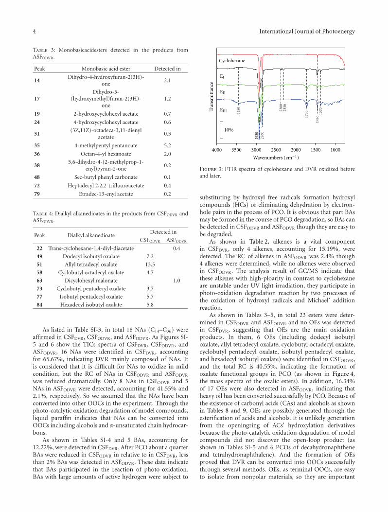
4 International Journal of Photoenergy
Table 3: Monobasicacidesters detected in the products fromASFODVR.
Peak Monobasic acid ester Detected in
14Dihydro-4-hydroxyfuran-2(3H)-
one2.1
17Dihydro-5-
(hydroxymethyl)furan-2(3H)-one
1.2
19 2-hydroxycyclohexyl acetate 0.7
24 4-hydroxycyclohexyl acetate 0.6
31(3Z,11Z)-octadeca-3,11-dienyl
acetate0.3
35 4-methylpentyl pentanoate 5.2
36 Octan-4-yl hexanoate 2.0
385,6-dihydro-4-(2-methylprop-1-
enyl)pyran-2-one0.2
48 Sec-butyl phenyl carbonate 0.1
72 Heptadecyl 2,2,2-trifluoroacetate 0.4
79 Etradec-13-enyl acetate 0.2
Table 4: Dialkyl alkanedioates in the products from CSFODVR andASFODVR.
Peak Dialkyl alkanedioateDetected in
CSFODVR ASFODVR
22 Trans-cyclohexane-1,4-diyl-diacetate 0.4
49 Dodecyl isobutyl oxalate 7.2
51 Allyl tetradecyl oxalate 13.5
58 Cyclobutyl octadecyl oxalate 4.7
63 Dicyclohexyl malonate 1.0
73 Cyclobutyl pentadecyl oxalate 3.7
77 Isobutyl pentadecyl oxalate 5.7
84 Hexadecyl isobutyl oxalate 5.8
As listed in Table SI-3, in total 18 NAs (C14–C36) wereaffirmed in CSFDVR, CSFODVR, and ASFODVR. As Figures SI-5 and 6 show the TICs spectra of CSFDVR, CSFODVR, andASFODVR, 16 NAs were identified in CSFDVR, accountingfor 65.67%, indicating DVR mainly composed of NAs. Itis considered that it is difficult for NAs to oxidize in mildcondition, but the RC of NAs in CSFODVR and ASFODVR
was reduced dramatically. Only 8 NAs in CSFODVR and 5NAs in ASFODVR were detected, accounting for 41.55% and2.1%, respectively. So we assumed that the NAs have beenconverted into other OOCs in the experiment. Through thephoto-catalytic oxidation degradation of model compounds,liquid paraffin indicates that NAs can be converted intoOOCs including alcohols and α-unsaturated chain hydrocar-bons.
As shown in Tables SI-4 and 5 BAs, accounting for12.22%, were detected in CSFDVR. After PCO about a quarterBAs were reduced in CSFODVR in relative to in CSFDVR, lessthan 2% BAs was detected in ASFODVR. These data indicatethat BAs participated in the reaction of photo-oxidation.BAs with large amounts of active hydrogen were subject to
4000 3500 3000 2500 2000 1500 1000
Tran
smit
tan
ce
Cyclohexane
EI
EII
EIII
1370
146017
30
2330
2380
2860
2930
3480
Wavenumbers (cm−1)
10%
Figure 3: FTIR spectra of cyclohexane and DVR oxidized beforeand later.
substituting by hydroxyl free radicals formation hydroxylcompounds (HCs) or eliminating dehydration by electron-hole pairs in the process of PCO. It is obvious that part BAsmay be formed in the course of PCO degradation, so BAs canbe detected in CSFODVR and ASFODVR though they are easy tobe degraded.
As shown in Table 2, alkenes is a vital componentin CSFDVR, only 4 alkenes, accounting for 15.19%, weredetected. The RC of alkenes in ASFODVR was 2.4% though4 alkenes were determined, while no alkenes were observedin CSFODVR. The analysis result of GC/MS indicate thatthese alkenes with high-ploarity in contrast to cyclohexaneare unstable under UV light irradiation, they participate inphoto-oxidation degradation reaction by two processes ofthe oxidation of hydroxyl radicals and Michael’ additionreaction.
As shown in Tables 3–5, in total 23 esters were deter-mined in CSFODVR and ASFODVR and no OEs was detectedin CSFDVR, suggesting that OEs are the main oxidationproducts. In them, 6 OEs (including dodecyl isobutyloxalate, allyl tetradecyl oxalate, cyclobutyl octadecyl oxalate,cyclobutyl pentadecyl oxalate, isobutyl pentadecyl oxalate,and hexadecyl isobutyl oxalate) were identified in CSFODVR,and the total RC is 40.55%, indicating the formation ofoxalate functional groups in PCO (as shown in Figure 4,the mass spectra of the oxalic esters). In addition, 16.34%of 17 OEs were also detected in ASFODVR, indicating thatheavy oil has been converted successfully by PCO. Because ofthe existence of carbonyl acids (CAs) and alcohols as shownin Tables 8 and 9, OEs are possibly generated through theesterification of acids and alcohols. It is unlikely generationfrom the openingring of ACs’ hydroxylation derivativesbecause the photo-catalytic oxidation degradation of modelcompounds did not discover the open-loop product (asshown in Tables SI-5 and 6 PCOs of decahydronaphtheneand tetrahydronaphthalene). And the formation of OEsproved that DVR can be converted into OOCs successfullythrough several methods. OEs, as terminal OOCs, are easyto isolate from nonpolar materials, so they are important

International Journal of Photoenergy 5
Table 5: Dialkyl phthalates detected in the products from ASFODVR.
Peak Dialkyl phthalate Detected in Peak Dialkyl phthalate Detected in
52 Diethyl phthalate 0.5 74 Butyl octyl phthalate 0.4
57 Diisobutyl phthalate 0.9 91 Bis(6-methylheptyl)phthalate 0.1
Table 6: Acids detected in the products from ASFODVR.
Peak Acid Detected in Peak Acid Detected in
2 Hexanoic acid 0.4 33 Oxepane-2,7-dione 3.7
5 4-oxopentanoic acid 25.1 40 Dodecanoic acid 0.2
12 5-oxohexanoic acid 1.6 45 Tridecanoic acid 0.3
13 3-(ethoxycarbonyl)propanoic acid 0.8 47 Tetradecanoic acid 0.4
15 1,3-dioxol-2-one 0.4 56 Pentadecanoic acid 0.3
23 Succinic acid 0.1 64 n-hexadecanoic acid 0.3
27 Glutaric acid 3.0 65 Palmitic acid 0.3
Table 7: Alcohols detected in the products from CSFDVR, CSFODVR and ASFODVR.
Peak AlcoholDetected in
CSFDVR CSFODVR ASFODVR
6 (1R,2R)-cyclohexane-1,2-diol 2.9
11 2,2-dimethyloctan-3-ol 5.9
16 4-methylheptan-3-ol 1.0
29 2,5-dimethylhex-4-en-3-ol 0.2
30 Tridecan-7-ol 0.4
39 2-octadecylpropane-1,3-diol 0.7
60 Hexadecane-1,2-diol 0.2
62 2-methyl-5,5-diphenylpenta-3,4-dien-2-ol 0.3
90 2-(octadecyloxy)ethanol 2.0 1.9
Table 8: Phenols detected in the products from ASFODVR.
Peak Phenol Detected in
3 Phenol 0.1
88 2,4-bis (2-phenylpropan-2-yl)phenol 1.4
industrial raw materials. Among them, oxalates always areconsidered as a main intermediate to make the cold lightilluminator or other military supplies. Hence, the conversionof compounds in PCO provides an effective approach tomake the DVR utilization effective.
As listed in Table 6, CAs are one of the OOCs and merelydetected in ASFODVR, suggesting that CAs as final productsare strongly polarity matters. As Figure 5 has shown that theRC of CAs is 36.4%, and compound 5 (shown in Figure SI-6and in Figure 5) is the most abundant account for 25.58% inASFODVR. OKs and ACs were also detected only in ASFODVR,as shown in Tables 9 and 10, and the RC of them is 8.79%and 1.13%, respectively, indicating that carbonyl compoundshave been formed in the reaction, and the primary productscan react continuously with each other through the additionreaction cyclopolymerization. From the upper analysis result,we suppose that the solvent participated in the reaction butwithout the formation of ring opening components. The
formation of compounds containing cyclohexane provideda proof that the active hydrogens were attacked by hydroxylsand obtained the production of cyclohexyl free radicals.
As illustrated in Tables 7 and 8, in total 10 HCs (includingalcohols and phenols) were detected, among them, one HCin CSFDVR, 2 HCs in CSFODVR and 7 HCs in ASFODVR. InASFODVR 2,2-dimethyloctan-3-ol (compound 11 in FigureSI-6) is the most abundant, accounting for ∼5.94% ofOMs, while ∼1.86% of OMs in CSFODVR. The formation of(1R,2R)-cyclohexane-1,2-diol suggests that OMs in DVR canbe oxidized by hydroxyl substitution besides cyclohexane.These facts indicate that hydroxyl oxidation is a mainstep in photo-oxidation process. It must be consideredas the mechanism causing the ring-opening reaction ofcyclohexane, but the products of ring opening were almostnot detected in the products of pure cyclohexane oxidation,so it is sure that active hydrogen in DVR has been substitutedby hydroxyl free radicals and led to the formation of theseHCs. The RC of HCs in CSFODVR is less than that inASFODVR, indicating the HCs with high polar. In addition,one HC exists in CSFDVR, and it is unsteady and easy todepolymerization.
As listed in Table 11, in total 11 ECs were detected 2-((dodecyloxy)methyl)oxirane appeared both in CSFDVR andCSFODVR simultaneously, whereas 10 ECs were detected in
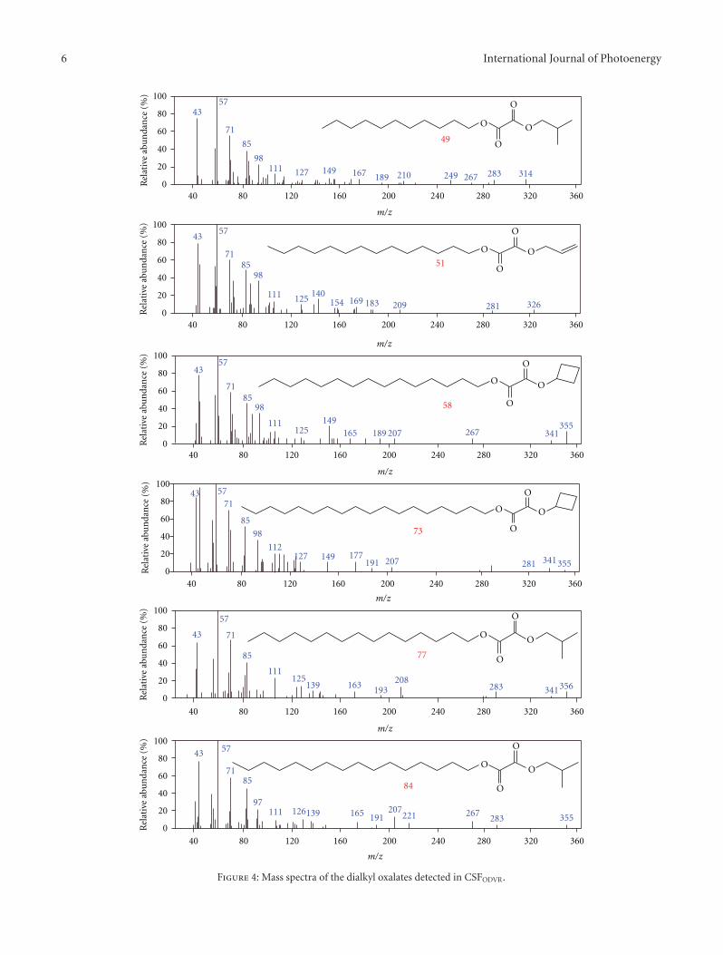
6 International Journal of Photoenergy
40
0
20
60
80
100
O
O
O
O
189 267
49
4357
71
85
98111 127 149 167 210 283249 314
m/z
36040 80 120 160 200 240 280 320
Rel
ativ
eab
un
dan
ce(%
)
40
0
20
60
80
10043
57
7185
98
111 125140
169281 326154 183 209
m/z
36040 80 120 160 200 240 280 320
OO
O
O
Rel
ativ
eab
un
dan
ce(%
)
51
40
0
20
60
80
100
58
355
4357
7185
98
111125
149165 189 207 267 341
m/z
36040 80 120 160 200 240 280 320
O O
O
O
Rel
ativ
eab
un
dan
ce(%
)
7340
0
20
60
80
10043 57
71
85
98
112127 149 177
191 207
m/z
36040 80 120 160 200 240 280 320
O
O
O
O
Rel
ativ
eab
un
dan
ce(%
)
281 341355
Rel
ativ
eab
un
dan
ce(%
)
77
356341283208
193163139
125111
85
71
57
43
0
20
60
80
100
m/z
36040
40
80 120 160 200 240 280 320
O
O
O
O
0
20
60
80
100
m/z
36040
40
80 120 160 200 240 280 320
43 57
7185
97111 126139 165 191
207 267283221 355
84
Rel
ativ
eab
un
dan
ce(%
)
O
O
O
O
Figure 4: Mass spectra of the dialkyl oxalates detected in CSFODVR.

International Journal of Photoenergy 7
Table 9: Ketones detected in the products from ASFODVR.
Peak Ketone Detected in Peak Ketone Detected in
1 Cyclohex-2-enone 0.6 32 3-hydroxycyclohexanone 7.2
8 Cyclohexane-1,4-dione 0.3 38 5,6-dihydro-4-(2-methylprop-1-enyl)pyran-2-one 0.2
10 4-hydroxycyclohexanone 0.3 75 Anthracene-9,10-dione 0.6
Table 10: ACs detected in the products from ASFODVR.
Peak AC Detected in Peak AC Detected in
9 (4as,8as)-decahydronaphthalene 0.7 55 Phenanthrene 0.1
53 Anthracene 0.2 81 9,10-dichloroanthracene 0.1
Table 11: ECs detected in the products from CSFDVR, CSFODVR and ASFODVR.
Peak Epoxy compoundDetected in
CSFDVR CSFODVR ASFODVR
4 dihydrofuran-2,5-dione 6.7
7 2-propylfuran 0.4
18 3,4-dimethylfuran-2,5-dione 0.3
21 4,5-dimethyl-2-pentadecyl-1,3-dioxolane 0.4
25 tetrahydro-3-methyl-5-oxofuran-2-carboxylic 5.8
26 isobenzofuran-1,3-dione 1.5
28 tetrahydro-5-oxofuran-2-carboxylic acid 0.5
34 5-heptyl-dihydrofuran-2(3H)-one 1.4
46 dihydro-5-(hydroxymethyl)furan-2(3H)-one 0.5
87 3-(tetrahydro-5-oxofuran-2-yl)propanoic 0.3
97 2-((dodecyloxy)methyl)oxirane 4.9 6.3
ASFODVR and most of them are rich with pentaheterocycles(such as furan, lactone, and acid anhydrides). The reasonis that the electron pair in hydroxyl oxygen atoms attackedthe active hydrogen in the same link and formed a ringand then formed the stable structure in organic molecularon account of losing the proton. This is the electrophilicsubstitution reaction. Furthermore, the relative contentof penta-heterocycles is the highest (account for 17.82%)mainly because of the small ring strain and the stable ringstructure [24].
3.4. Mass Spectra Analyses of Oxalate in CSFODVR. Asexhibited in Figure 4, six oxalates in CSFODVR were identifiedwith large number of RC. These compounds in peaks 49,51, 58, 73, 77, and 84 (as shown in Figure SI-5) seem tobe oxalate containing because of the fragments at m/z 207.The molecular ions M+ at m/z 356 are compounds 73 and77, and compound 49 is at m/z 314 and compound 51 isat m/z 326, but the molecular ions of the compounds 58and 84 disappear. If the peak at m/z 207 was consideredas column loss or other impurity peaks, the mass spectrashape of oxalates should be similar to that of NAs. However,the oxalates were determined with GC/MS analyses andacquired processes using Chemstation software with NIST05library data. In addition, the structure of compounds 58and 73 is cis-, but the structures of compounds 49, 51, 77,and 84 are trans-, indicating the cis-formation of oxalates
with cyclobutane as branched-chain more stable than thecorresponding trans-forms. However, the trans-formation ofoxalates with branched chain alkanes or unsaturated is morestable than the corresponding trans-forms. The possiblereason is that the substitutions meet with different sterichindrance. The stereohindrance effect of cyclobutane and therepulsion force between a pair of electrons cause the carbon-carbon bond formation in oxalate rotation.
3.5. Mechanics of Photo-Oxidation Degrading DVR. Asshown in Figure 5, five species OMs in CSFDVR wereconverted into five species of OMs in CSFODVR and ninespecies of OMs in ASFODVR, presenting the diversifiedproducts formed. Key steps of the products transformationare as follows. Firstly, the active hydrogen from methyl ormethylene in NAs, BAs or branched-chain aromatics couldbe substituted by the hydroxyls generated on the surface ofTiO2 with H2O2 in the process priority, and lead to formHCs. Some HCs eliminate water molecular to form UCs, andUCs in ASFODVR product easily undergo Michael additionreaction and generate lactone rings or cyclic ethers (such asfuran or acid anhydrides). In addition, some HCs or UCscan also be converted into OKs or CAs and other OEs byhydroxyl radicals attack. The facts proved that alkanes, notonly BAs or ACs with branched chain, can be oxidized in theprocesses. Secondly, the biomarkers through bond breaking,ring opening, and small molecules eliminated could be
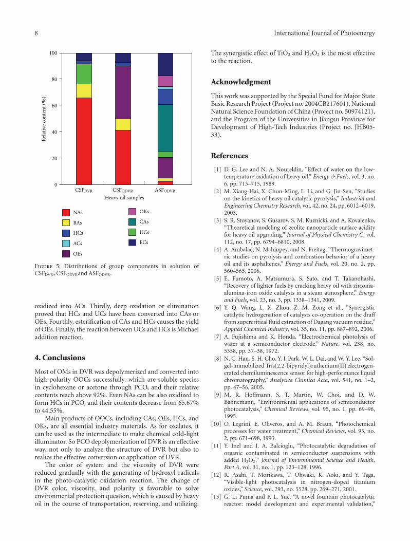
8 International Journal of Photoenergy
CSFDVR CSFODVR ASFODVR
NAs
BAs
HCs
ACs
OEs
OKs
CAs
UCs
ECs
20
40
60
80
100
0
Rel
ativ
eco
nte
nt
(%)
Heavy oil samples
Figure 5: Distributions of group components in solution ofCSFDVR, CSFODVRand ASFODVR.
oxidized into ACs. Thirdly, deep oxidation or eliminationproved that HCs and UCs have been converted into CAs orOEs. Fourthly, esterification of CAs and HCs causes the yieldof OEs. Finally, the reaction between UCs and HCs is Michaeladdition reaction.
4. Conclusions
Most of OMs in DVR was depolymerized and converted intohigh-polarity OOCs successfully, which are soluble speciesin cyclohexane or acetone through PCO, and their relativecontents reach above 92%. Even NAs can be also oxidized toform HCs in PCO, and their contents decrease from 65.67%to 44.55%.
Main products of OOCs, including CAs, OEs, HCs, andOKs, are all essential industry materials. As for oxalates, itcan be used as the intermediate to make chemical cold-lightilluminator. So PCO depolymerization of DVR is an effectiveway, not only to analyze the structure of DVR but also torealize the effective conversion or application of DVR.
The color of system and the viscosity of DVR werereduced gradually with the generating of hydroxyl radicalsin the photo-catalytic oxidation reaction. The change ofDVR color, viscosity, and polarity is favorable to solveenvironmental protection question, which is caused by heavyoil in the course of transportation, reserving, and utilizing.
The synergistic effect of TiO2 and H2O2 is the most effectiveto the reaction.
Acknowledgment
This work was supported by the Special Fund for Major StateBasic Research Project (Project no. 2004CB217601), NationalNatural Science Foundation of China (Project no. 50974121),and the Program of the Universities in Jiangsu Province forDevelopment of High-Tech Industries (Project no. JHB05-33).
References
[1] D. G. Lee and N. A. Noureldin, “Effect of water on the low-temperature oxidation of heavy oil,” Energy & Fuels, vol. 3, no.6, pp. 713–715, 1989.
[2] M. Xiang-Hai, X. Chun-Ming, L. Li, and G. Jin-Sen, “Studieson the kinetics of heavy oil catalytic pyrolysis,” Industrial andEngineering Chemistry Research, vol. 42, no. 24, pp. 6012–6019,2003.
[3] S. R. Stoyanov, S. Gusarov, S. M. Kuznicki, and A. Kovalenko,“Theoretical modeling of zeolite nanoparticle surface acidityfor heavy oil upgrading,” Journal of Physical Chemistry C, vol.112, no. 17, pp. 6794–6810, 2008.
[4] A. Ambalae, N. Mahinpey, and N. Freitag, “Thermogravimet-ric studies on pyrolysis and combustion behavior of a heavyoil and its asphaltenes,” Energy and Fuels, vol. 20, no. 2, pp.560–565, 2006.
[5] E. Fumoto, A. Matsumura, S. Sato, and T. Takanohashi,“Recovery of lighter fuels by cracking heavy oil with zirconia-alumina-iron oxide catalysts in a steam atmosphere,” Energyand Fuels, vol. 23, no. 3, pp. 1338–1341, 2009.
[6] Y. Q. Wang, L. X. Zhou, Z. M. Zong et al., “Synergisticcatalytic hydrogenation of catalysts co-operation on the drafffrom supercritical fluid extraction of Dagang vacuum residue,”Applied Chemical Industry, vol. 35, no. 11, pp. 887–892, 2006.
[7] A. Fujishima and K. Honda, “Electrochemical photolysis ofwater at a semiconductor electrode,” Nature, vol. 238, no.5358, pp. 37–38, 1972.
[8] N. C. Han, S. H. Cho, Y. J. Park, W. L. Dai, and W. Y. Lee, “Sol-gel-immobilized Tris(2,2-bipyridyl)ruthenium(II) electrogen-erated chemiluminescence sensor for high-performance liquidchromatography,” Analytica Chimica Acta, vol. 541, no. 1–2,pp. 47–56, 2005.
[9] M. R. Hoffmann, S. T. Martin, W. Choi, and D. W.Bahnemann, “Environmental applications of semiconductorphotocatalysis,” Chemical Reviews, vol. 95, no. 1, pp. 69–96,1995.
[10] O. Legrini, E. Oliveros, and A. M. Braun, “Photochemicalprocesses for water treatment,” Chemical Reviews, vol. 93, no.2, pp. 671–698, 1993.
[11] Y. Inel and I. A. Balcioglu, “Photocatalytic degradation oforganic contaminated in semiconductor suspensions withadded H2O2,” Journal of Environmental Science and Health,Part A, vol. 31, no. 1, pp. 123–128, 1996.
[12] R. Asahi, T. Morikawa, T. Ohwaki, K. Aoki, and Y. Taga,“Visible-light photocatalysis in nitrogen-doped titaniumoxides,” Science, vol. 293, no. 5528, pp. 269–271, 2001.
[13] G. Li Puma and P. L. Yue, “A novel fountain photocatalyticreactor: model development and experimental validation,”

International Journal of Photoenergy 9
Chemical Engineering Science, vol. 56, no. 8, pp. 2733–2744,2001.
[14] W. Cui, L. Feng, C. Xu, S. Lu, and F. Qiu, “Hydrogenproduction by photocatalytic decomposition of methanol gason Pt/TiO2 nano-film,” Catalysis Communications, vol. 5, no.9, pp. 533–536, 2004.
[15] M. Zach, C. Hagglund, D. Chakarov, and B. Kasemo,“Nanoscience and nanotechnology for advanced energy sys-tems,” Current Opinion in Solid State and Materials Science,vol. 10, no. 3–4, pp. 132–143, 2006.
[16] K. Hashimoto, T. Kawai, and T. Sakata, “Photocatalytic reac-tions of hydrocarbons and fossil fuels with water. Hydrogenproduction and oxidation,” Journal of Physical Chemistry, vol.88, no. 18, pp. 4083–4088, 1984.
[17] R. Dlugi and H. Gusten, “The catalytic and photocatalyticactivity of coal fly ashes,” Atmospheric Environment, vol. 17,no. 9, pp. 1765–1771, 1983.
[18] R. F. Lee, “Photo-oxidation and photo-toxicity of crude andrefined oils,” Spill Science and Technology Bulletin, vol. 8, no. 2,pp. 157–162, 2003.
[19] J. G. Fang and G. H. Xu, “Research progress in the synthesisof oxalate,” Chemical Propell & Poly Mater, vol. 2, no. 2, pp.18–21, 2004.
[20] M. M. Rauhut, L. G. Bollyky, and B. G. Roberts, “Chemiluminescence from reactions of electrtro-negatively substitutedaryl oxalates with hydrogen peroxide and fluorescent com-pounds,” Journal of the American Chemical Society, vol. 89, no.25, pp. 6515–6522, 1967.
[21] D. M. Fenton and P. J. Steinwand, “Preparation of oxalates,”1967, US P 3393136.
[22] D. M. Fenton and P. J. Steinwand, “Noble metal catalysis IVpreparation of dialkyl oxalates by oxidative carbonylation,”Journal of Organic Chemistry, vol. 39, no. 5, pp. 701–703, 1974.
[23] H. S. Xie, Y. R. Zhu, A. M. Li, and L. Lu, “Application of TiO2
powder in treating wastewater from paper-making factory,”Photographic Science and Photochemistry, vol. 24, no. 4, pp.312–317, 2006.
[24] S. W. Bi, B. Wang, and Y. Z. Gao, “Mechanistic study onreaction of [Cp∗Rh(CO)2Me]BF4 with NBD,” Chinese Journalof Inorganic Chemistry, vol. 22, no. 1, pp. 13–20, 2006.
Hindawi Publishing CorporationInternational Journal of PhotoenergyVolume 2011, Article ID 762929, 5 pagesdoi:10.1155/2011/762929
Research Article
Photocatalytic Activity of Nanosized Cadmium SulfidesSynthesized by Complex Compound Thermolysis
Yingchun Yu, Youxian Ding, Shengli Zuo, and Jianjun Liu
Faculty of Sciences, Beijing University of Chemical Technology, Beijing 100029, China
Correspondence should be addressed to Jianjun Liu, [email protected]
Received 15 June 2010; Accepted 15 August 2010
Academic Editor: Mohamed Sabry Abdel-Mottaleb
Copyright © 2011 Yingchun Yu et al. This is an open access article distributed under the Creative Commons Attribution License,which permits unrestricted use, distribution, and reproduction in any medium, provided the original work is properly cited.
The nanosized cadmium sulfides (CdSs) containing different phase structures were synthesized via the complex compoundthermolysis method using different molar ratio of thiourea to acetate cadmium (S/Cd) and characterized by XRD, TEM, UV-Vis, and IR spectra. The results of photocatalytic degradation of rhodamine B (RB) show that the activity order of CdS concerningthe phase compositions is of cubic > hexagonal > cubic + hexagonal, where the CdS with the cubic phase has the best photocatalyticdegradation activity of RB due to its larger abilities of adsorption and absorbance and smaller particle size of about 10∼13 nm.
1. Introduction
Nanomaterials are assemblies with particles or crystal sizebetween 1 nm and 100 nm, which include different typesof nanoparticles, nanowires, nanotubes, and nanofilms andother nanobulk materials. Nanomaterials possess manyunique physical and chemical properties different from theirbulk counterparts due to the obvious quantum size effectand small size effect [1, 2]. Photocatalysis is one of the keytechnologies to solve both energy and environmental prob-lems using solar energy, in which an efficient photocatalystis necessary. Although remarkable progress has been madein recent years for photocatalysts working under ultravioletlight, there are limitations for the photocatalysts to beapplied under visible light. The problem could be resolvedby using visible light-induced photocatalysts with properband gap energy, such as CdS, WO3, or Fe2O3. AlthoughCdS is a good candidate for photocatalytic water reductionand pollutant oxidation, it has the fatal photocorrosionproblem due to the oxidation of itself by the photogeneratedhole [3]. Usually, CdSs are of cubic phase and hexagonalphase and the cubic phase can transform into hexagonalone when heated to certain temperatures [4]. At present,there are many studies on the synthesis of hexagonal CdS.Lin et al. [5] and Bao et al. [6] found that the hexagonal
CdS nanoparticles synthesized via solvothermal methodhave much better photocatalytic activity for degradation ofmethylene blue and better hydrogen production activity forwater photolysis, using thiourea and cadmium acetate as rawmaterials. Jing and Guo [7] reported a CdS catalyst systemwith a high hydrogen production activity for water photolysisusing cadmium acetate as cadmium source and H2S as sulfursource. The CdS synthesized under solvothermal or heatingconditions is usually of stable hexagonal phase, but there area few reports on the synthesis of metastable cubic CdS. Manyfactors can influence the photocatalytic activity of CdS, suchas phase composition, crystallite size, morphology, specificsurface area, and energy gap. For example, Degussa P25(made in Germany), a type of commercial nanosized titaniawhich possesses a high photocatalytic activity, exists in poly-morphs composed of about 80% anatase and 20% rutile [8].Therefore, it is very important to study how to get the CdSphotocatalysts with different phase compositions and theirphotocatalytic activities by controlling reaction conditions.
In this study, the CdS nanocrystals with different phasecompositions were synthesized via thermal decompositionof thiourea-cadmium complexes using cadmium acetate andthiourea as raw materials. The photocatalytic activities ofthe synthesized CdS nanocrystals for the degradation ofRhodamine B under visible light were also studied.
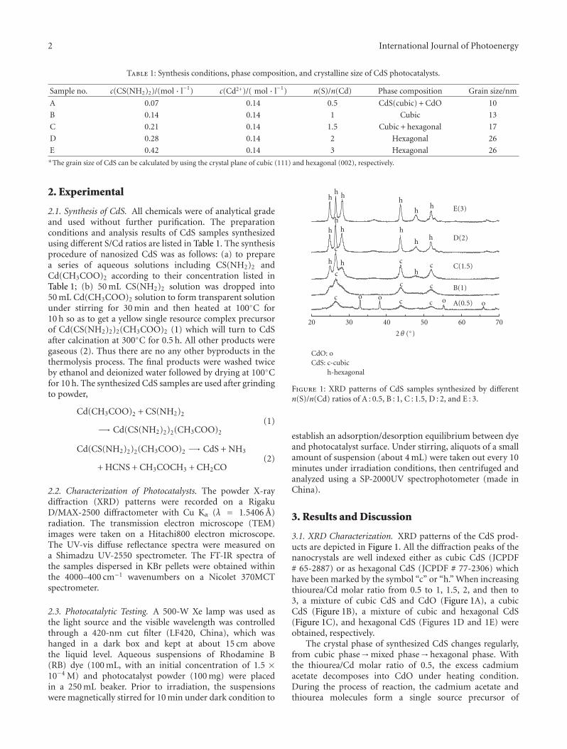
2 International Journal of Photoenergy
Table 1: Synthesis conditions, phase composition, and crystalline size of CdS photocatalysts.
Sample no. c(CS(NH2)2)/(mol · l−1) c(Cd2+)/( mol · l−1) n(S)/n(Cd) Phase composition Grain size/nm
A 0.07 0.14 0.5 CdS(cubic) + CdO 10
B 0.14 0.14 1 Cubic 13
C 0.21 0.14 1.5 Cubic + hexagonal 17
D 0.28 0.14 2 Hexagonal 26
E 0.42 0.14 3 Hexagonal 26∗The grain size of CdS can be calculated by using the crystal plane of cubic (111) and hexagonal (002), respectively.
2. Experimental
2.1. Synthesis of CdS. All chemicals were of analytical gradeand used without further purification. The preparationconditions and analysis results of CdS samples synthesizedusing different S/Cd ratios are listed in Table 1. The synthesisprocedure of nanosized CdS was as follows: (a) to preparea series of aqueous solutions including CS(NH2)2 andCd(CH3COO)2 according to their concentration listed inTable 1; (b) 50 mL CS(NH2)2 solution was dropped into50 mL Cd(CH3COO)2 solution to form transparent solutionunder stirring for 30 min and then heated at 100◦C for10 h so as to get a yellow single resource complex precursorof Cd(CS(NH2)2)2(CH3COO)2 (1) which will turn to CdSafter calcination at 300◦C for 0.5 h. All other products weregaseous (2). Thus there are no any other byproducts in thethermolysis process. The final products were washed twiceby ethanol and deionized water followed by drying at 100◦Cfor 10 h. The synthesized CdS samples are used after grindingto powder,
Cd(CH3COO)2 + CS(NH2)2
−→ Cd(CS(NH2)2)2(CH3COO)2
(1)
Cd(CS(NH2)2)2(CH3COO)2 −→ CdS + NH3
+ HCNS + CH3COCH3 + CH2CO(2)
2.2. Characterization of Photocatalysts. The powder X-raydiffraction (XRD) patterns were recorded on a RigakuD/MAX-2500 diffractometer with Cu Kα (λ = 1.5406 A)radiation. The transmission electron microscope (TEM)images were taken on a Hitachi800 electron microscope.The UV-vis diffuse reflectance spectra were measured ona Shimadzu UV-2550 spectrometer. The FT-IR spectra ofthe samples dispersed in KBr pellets were obtained withinthe 4000–400 cm−1 wavenumbers on a Nicolet 370MCTspectrometer.
2.3. Photocatalytic Testing. A 500-W Xe lamp was used asthe light source and the visible wavelength was controlledthrough a 420-nm cut filter (LF420, China), which washanged in a dark box and kept at about 15 cm abovethe liquid level. Aqueous suspensions of Rhodamine B(RB) dye (100 mL, with an initial concentration of 1.5 ×10⁻⁴ M) and photocatalyst powder (100 mg) were placedin a 250 mL beaker. Prior to irradiation, the suspensionswere magnetically stirred for 10 min under dark condition to
20 30 40 50 60 70
2 θ (◦)
c o o c c o oA(0.5)
c
c c B(1)
h
c
h c
hc C(1.5)
h
hh h
hh D(2)
hh h
h
hh E(3)
CdO: oCdS: c-cubic
h-hexagonal
Figure 1: XRD patterns of CdS samples synthesized by differentn(S)/n(Cd) ratios of A : 0.5, B : 1, C : 1.5, D : 2, and E : 3.
establish an adsorption/desorption equilibrium between dyeand photocatalyst surface. Under stirring, aliquots of a smallamount of suspension (about 4 mL) were taken out every 10minutes under irradiation conditions, then centrifuged andanalyzed using a SP-2000UV spectrophotometer (made inChina).
3. Results and Discussion
3.1. XRD Characterization. XRD patterns of the CdS prod-ucts are depicted in Figure 1. All the diffraction peaks of thenanocrystals are well indexed either as cubic CdS (JCPDF# 65-2887) or as hexagonal CdS (JCPDF # 77-2306) whichhave been marked by the symbol “c” or “h.” When increasingthiourea/Cd molar ratio from 0.5 to 1, 1.5, 2, and then to3, a mixture of cubic CdS and CdO (Figure 1A), a cubicCdS (Figure 1B), a mixture of cubic and hexagonal CdS(Figure 1C), and hexagonal CdS (Figures 1D and 1E) wereobtained, respectively.
The crystal phase of synthesized CdS changes regularly,from cubic phase→mixed phase→hexagonal phase. Withthe thiourea/Cd molar ratio of 0.5, the excess cadmiumacetate decomposes into CdO under heating condition.During the process of reaction, the cadmium acetate andthiourea molecules form a single source precursor of
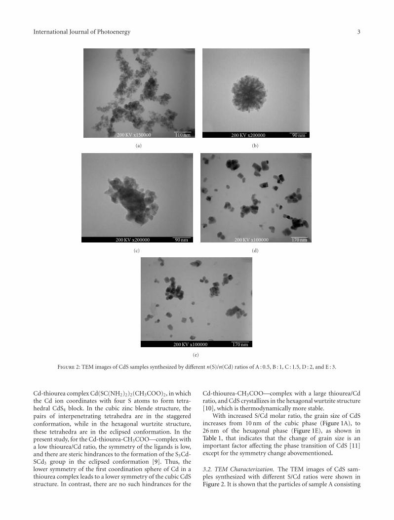
International Journal of Photoenergy 3
200 KV x150000 110 nm
(a)
200 KV x200000 90 nm
(b)
200 KV x200000 90 nm
(c)
200 KV x100000 170 nm
(d)
200 KV x100000 170 nm
(e)
Figure 2: TEM images of CdS samples synthesized by different n(S)/n(Cd) ratios of A : 0.5, B : 1, C : 1.5, D : 2, and E : 3.
Cd-thiourea complex Cd(SC(NH2)2)2(CH3COO)2, in whichthe Cd ion coordinates with four S atoms to form tetra-hedral CdS4 block. In the cubic zinc blende structure, thepairs of interpenetrating tetrahedra are in the staggeredconformation, while in the hexagonal wurtzite structure,these tetrahedra are in the eclipsed conformation. In thepresent study, for the Cd-thiourea-CH3COO—complex witha low thiourea/Cd ratio, the symmetry of the ligands is low,and there are steric hindrances to the formation of the S3Cd-SCd3 group in the eclipsed conformation [9]. Thus, thelower symmetry of the first coordination sphere of Cd in athiourea complex leads to a lower symmetry of the cubic CdSstructure. In contrast, there are no such hindrances for the
Cd-thiourea-CH3COO—complex with a large thiourea/Cdratio, and CdS crystallizes in the hexagonal wurtzite structure[10], which is thermodynamically more stable.
With increased S/Cd molar ratio, the grain size of CdSincreases from 10 nm of the cubic phase (Figure 1A), to26 nm of the hexagonal phase (Figure 1E), as shown inTable 1, that indicates that the change of grain size is animportant factor affecting the phase transition of CdS [11]except for the symmetry change abovementioned.
3.2. TEM Characterization. The TEM images of CdS sam-ples synthesized with different S/Cd ratios were shown inFigure 2. It is shown that the particles of sample A consisting
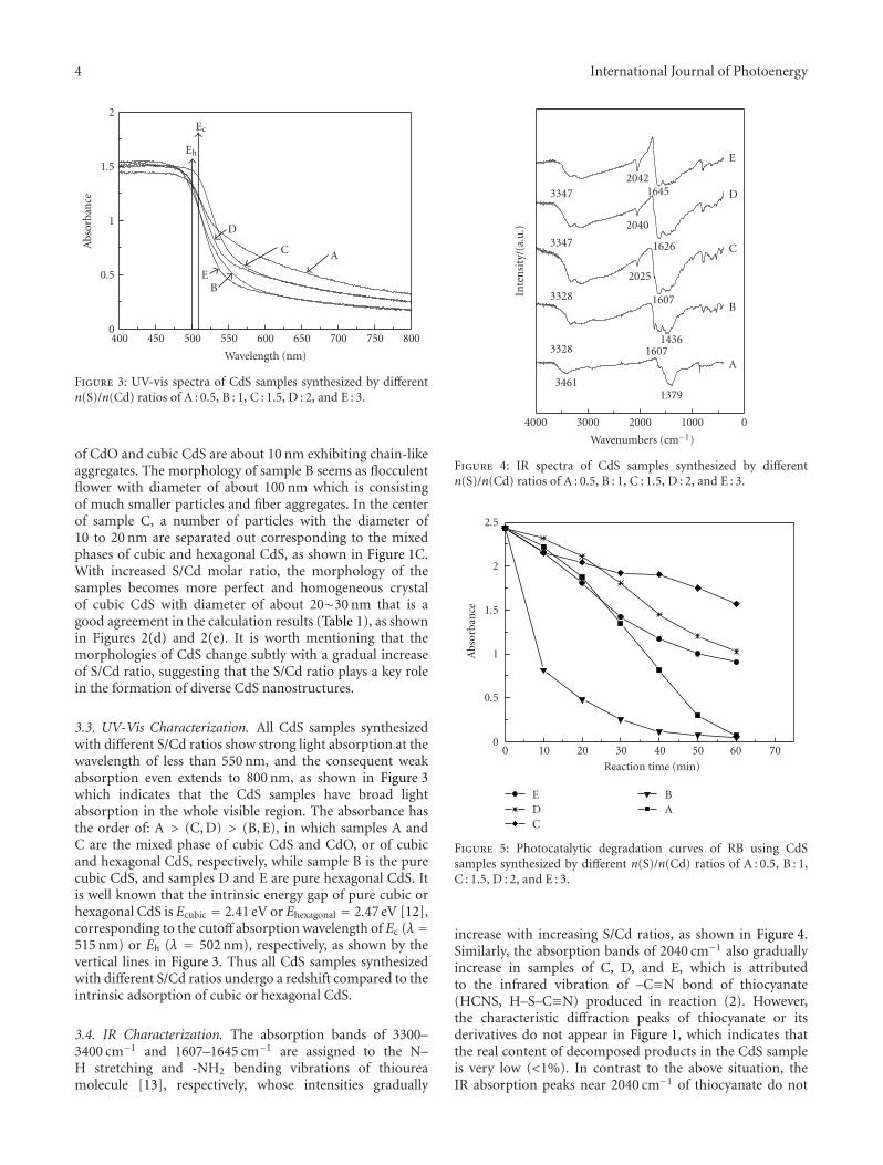
4 International Journal of Photoenergy
400 450 500 550 600 650 700 750 800
Wavelength (nm)
0
0.5
1
1.5
2
Abs
orba
nce
EB
C A
D
Ec
Eh
Figure 3: UV-vis spectra of CdS samples synthesized by differentn(S)/n(Cd) ratios of A : 0.5, B : 1, C : 1.5, D : 2, and E : 3.
of CdO and cubic CdS are about 10 nm exhibiting chain-likeaggregates. The morphology of sample B seems as flocculentflower with diameter of about 100 nm which is consistingof much smaller particles and fiber aggregates. In the centerof sample C, a number of particles with the diameter of10 to 20 nm are separated out corresponding to the mixedphases of cubic and hexagonal CdS, as shown in Figure 1C.With increased S/Cd molar ratio, the morphology of thesamples becomes more perfect and homogeneous crystalof cubic CdS with diameter of about 20∼30 nm that is agood agreement in the calculation results (Table 1), as shownin Figures 2(d) and 2(e). It is worth mentioning that themorphologies of CdS change subtly with a gradual increaseof S/Cd ratio, suggesting that the S/Cd ratio plays a key rolein the formation of diverse CdS nanostructures.
3.3. UV-Vis Characterization. All CdS samples synthesizedwith different S/Cd ratios show strong light absorption at thewavelength of less than 550 nm, and the consequent weakabsorption even extends to 800 nm, as shown in Figure 3which indicates that the CdS samples have broad lightabsorption in the whole visible region. The absorbance hasthe order of: A > (C, D) > (B, E), in which samples A andC are the mixed phase of cubic CdS and CdO, or of cubicand hexagonal CdS, respectively, while sample B is the purecubic CdS, and samples D and E are pure hexagonal CdS. Itis well known that the intrinsic energy gap of pure cubic orhexagonal CdS is Ecubic = 2.41 eV or Ehexagonal = 2.47 eV [12],corresponding to the cutoff absorption wavelength of Ec (λ =515 nm) or Eh (λ = 502 nm), respectively, as shown by thevertical lines in Figure 3. Thus all CdS samples synthesizedwith different S/Cd ratios undergo a redshift compared to theintrinsic adsorption of cubic or hexagonal CdS.
3.4. IR Characterization. The absorption bands of 3300–3400 cm−1 and 1607–1645 cm−1 are assigned to the N–H stretching and -NH2 bending vibrations of thioureamolecule [13], respectively, whose intensities gradually
4000 3000 2000 1000 0
Wavenumbers (cm−1)
Inte
nsi
ty/(
a.u
.)
E
B
C
A
D
13793461
3328 16071436
16073328
2025
16263347
3347
2040
20421645
Figure 4: IR spectra of CdS samples synthesized by differentn(S)/n(Cd) ratios of A : 0.5, B : 1, C : 1.5, D : 2, and E : 3.
0 10 20 30 40 50 60 70
Reaction time (min)
0
0.5
1
1.5
2
2.5
Abs
orba
nce
EDC
BA
Figure 5: Photocatalytic degradation curves of RB using CdSsamples synthesized by different n(S)/n(Cd) ratios of A : 0.5, B : 1,C : 1.5, D : 2, and E : 3.
increase with increasing S/Cd ratios, as shown in Figure 4.Similarly, the absorption bands of 2040 cm−1 also graduallyincrease in samples of C, D, and E, which is attributedto the infrared vibration of –C≡N bond of thiocyanate(HCNS, H–S–C≡N) produced in reaction (2). However,the characteristic diffraction peaks of thiocyanate or itsderivatives do not appear in Figure 1, which indicates thatthe real content of decomposed products in the CdS sampleis very low (<1%). In contrast to the above situation, theIR absorption peaks near 2040 cm−1 of thiocyanate do not

International Journal of Photoenergy 5
appear in the samples of A(0.5) and B(1.0), indicatingthat there is no excess thiourea to be decomposed intothiocyanate.
3.5. Photocatalytic Activities. The curves of photocatalyticdegradation of RB using different CdS samples are shownin Figure 5. With the residual absorbance of RB after 60 minas evaluation index, the degradation activity is in the orderof B ≈ A > E > D > C. Sample B has relativelyrapid degradation within the first 10 min, which can beattributed to its strong adsorption of RB due to the flocculentparticle morphology with larger surface area, as shownin Figure 2(b). Furthermore, sample A has the strongestabsorption in visible region and the smallest grain size(10 nm), so it has a higher photocatalytic activity. Whilen(S)/n(Cd) > 1, the catalytic activities of samples E, D, andC are lower than that of A and B. It is known from Figure 4that the excess thiocyanate remains on the surface of samplesE, D, and C, in which the S2− ions can act as a photoinducedhole sacrificial reagent and compete with the oxidation of RBdye, resulting in the decrease of the photocatalytic activity[14]. On the other hand, the order of phase compositioneffect on the catalytic activity is cubic > hexagonal >mixed. As shown in Figure 2, the hexagonal CdS samplesof D and E are in good crystallinity and homogeneousparticle dispersion. However, the mixed phase CdS of C isan aggregate containing many defects between the two-phaseinterface, accounting for the lower photocatalytic activity.
4. Conclusions
The cubic CdS, hexagonal CdS, and their mixed phase weresynthesized under the conditions of thiourea/Cd (S/Cd)molar ratios (0.5∼3) of ≤1, ≥2, and 1.0∼1.5, respectively.The grain size of CdS increases with the increased S/Cd ratio.The photocatalytic activity is in order of cubic > hexagonal >mixed phase, in which the cubic phase CdS has the bestphotocatalytic activity for RB degradation due to its strongadsorption, intense absorbance in visible region, and thesmaller grain size.
Acknowledgments
This work was financially supported by the Chinese NationalTCM Project in the 11th Five-Year Period through the Grant2007BAK26B08. The authors acknowledge the Chinese Peo-ple’s Security University for its full cooperation.
References
[1] W. Kelsall, I. W. Hamley, and M. Geoghegan, Nanoscale Scienceand Technology, John Wiley & Sons, New York, NY, USA, 2005.
[2] C. P. Poole and F. J. Owens, Introduction to Nanotechnology,John Wiley & Sons, New York, NY, USA, 2003.
[3] D. Meissner, R. Memming, and B. Kastening, “Photoelectro-chemistry of cadmium sulfide. 1. reanalysis of photocorrosionand flat-band potential,” Journal of Physical Chemistry, vol. 92,no. 12, pp. 3476–3483, 1988.
[4] N. Sahu, M. K. Arora, S. N. Upadhyay, and A. S. K.Sinha, “Phase transformation and activity of cadmium sulfidephotocatalysts for hydrogen production from water: role ofadsorbed ammonia on cadmium sulfate precursor,” Industrialand Engineering Chemistry Research, vol. 37, no. 12, pp. 4682–4688, 1998.
[5] G. Lin, J. Zheng, and R. Xu, “Template-free synthesis ofuniform CdS hollow nanospheres and their photocatalyticactivities,” Journal of Physical Chemistry C, vol. 112, no. 19, pp.7363–7370, 2008.
[6] N. Bao, L. Shen, T. Takata et al., “Facile Cd—thiourea complexthermolysis synthesis of phase-controlled CdS nanocrystalsfor photocatalytic hydrogen production under visible light,”Journal of Physical Chemistry C, vol. 111, no. 47, pp. 17527–17534, 2007.
[7] D. Jing and L. Guo, “A novel method for the preparation ofa highly stable and active CdS photocatalyst with a specialsurface nanostructure,” Journal of Physical Chemistry B, vol.110, no. 23, pp. 11139–11145, 2006.
[8] J. Liu, W. Qin, S. Zuo, Y. Yu, and Z. Hao, “Solvothermal-induced phase transition and visible photocatalytic activity ofnitrogen-doped titania,” Journal of Hazardous Materials, vol.163, no. 1, pp. 273–278, 2009.
[9] A. V. Naumov, V. N. Semenov, and E. G. Goncharov,“Properties of CdS films prepared from thiourea complexes ofcadmium salts,” Inorganic Materials, vol. 37, no. 6, pp. 539–543, 2001.
[10] V. Swayambunathan, D. Hayes, K. H. Schmidt, Y. X. Liao,and D. Meisel, “Thiol surface complexation on growing CdSclusters,” Journal of the American Chemical Society, vol. 112,no. 10, pp. 3831–3837, 1990.
[11] N. Herron, Y. Wang, and H. Eckert, “Synthesis and char-acterization of surface-capped, size-quantized CdS clusters.Chemical control of cluster size,” Journal of the AmericanChemical Society, vol. 112, no. 4, pp. 1322–1326, 1990.
[12] D. J. Kim, Y.-M. Yu, J. W. Lee, and Y. D. Choi, “Investigationof energy band gap and optical properties of cubic CdSepilayers,” Applied Surface Science, vol. 254, no. 22, pp. 7522–7526, 2008.
[13] G. W. C. Kaye and T. H. Laby, Tables of Physical and ChemicalConstants, Longman Press, London, UK, 16th edition, 1995.
[14] I. Tsuji, H. Kato, and A. Kudo, “Photocatalytic hydrogenevolution on ZnS-CuInS2-AglnS2 solid solution photocata-lysts with wide visible light absorption bands,” Chemistry ofMaterials, vol. 18, no. 7, pp. 1969–1975, 2006.
Hindawi Publishing CorporationInternational Journal of PhotoenergyVolume 2011, Article ID 801409, 6 pagesdoi:10.1155/2011/801409
Research Article
Structure and Physical Properties of Polymer Composite FilmsDoped with Fullerene Nanoparticles
R. M. Ahmed1 and S. M. El-Bashir2, 3
1 Department of Physics, Faculty of Science, Zagazig University, Zagazig 44519, Egypt2 Department of Physics and Astronomy, Science College, King Saud University Riyadh 11451, Saudi Arabia3 Department of Physics, Faculty of Science, Banha University, Egypt
Correspondence should be addressed to R. M. Ahmed, rania8 [email protected]
Received 3 July 2010; Accepted 30 September 2010
Academic Editor: Mohamed Sabry Abdel-Mottaleb
Copyright © 2011 R. M. Ahmed and S. M. El-Bashir. This is an open access article distributed under the Creative CommonsAttribution License, which permits unrestricted use, distribution, and reproduction in any medium, provided the original work isproperly cited.
Fullerene C60 has stimulated intense interest for scientific, industrial, and medical community because of its unique structure andproperties. In the present study we prepared fullerene-doped nanocomposite films based on PMMA, PVAc, and PMMA/PVAcblend. Observations made by transmission electron microscope (TEM) showed the uniform dispersion of C60 nanoparticles inthe polymer matrices. Also, X-ray diffraction measurements indicated that C60 has a tendency to form crystallites in the polymermatrices. In addition, the concentration effect of fullerene C60 was investigated using optical absorption and photoluminescencespectroscopy. The spectroscopic properties of such films recommended their application in photonics and solar energy conversion.
1. Introduction
Recently, polymers are finding an important place in dif-ferent research laboratories for the study of their variousproperties [1]. Many polymers have been proved suitablematrices in the development of composite structures due totheir ease production and processing, good adhesion withreinforcing elements, resistance to corrosive environment,light weight, and in some cases ductile mechanical perfor-mance [2]. Fullerenes have been widely studied due to theirunique structural, electronic and spectroscopic properties,which may be exploited for their diverse applications inchemistry, biology, and nanoscience [3].
Lately interest of researchers engaged in different fieldsof knowledge is seen to be focused on determination of theaction of nanomaterial addition, such as fullerenes and nan-otubes, on properties of polymers and their compositions.Incorporation of fullerene and nanotubes into chemicalcomposition of polymers gives one more opportunities fortheir study and application as composite materials, films, andfibers serving different purposes [4].
Also, the research of polymer material has been directedto blend or copolymer of different polymers to obtain
new products having some of the desired properties ofeach component [5]. PMMA (polymethylmethacrylate) andits derivatives are known for their medical applications,particularly for hard tissue repair and regeneration. PMMAand (polyvinyl acetate) PVAc form an important and uniquepair of polymers although they are chemically different [6].
The aim of the present work concerns on studying thechange in the optical absorption, the optical parametersand photoluminescence spectra for the samples of fullerenepolymer composites which are recorded at room tempera-ture. In addition, X-ray diffraction (XRD) and transmissionelectron microscope (TEM) are used to characterize thefullerene/Polymer nanocomposites.
2. Materials and Methods
2.1. Materials. Both PMMA (poly methyl methacrylate)and PVAc (poly vinyl acetate) used in this study wereobtained from Sigma-Aldrich (Germany) and were reportedto have molecular weights of 996,000 and 167,000 g·mol−1,respectively. Moreover, Buckminster fullerene powder C60,has purity of 97% and Mr = 720.66 and was obtained fromFluka (USA). In addition, chloroform has purity of 99.8%

2 International Journal of Photoenergy
100 nm
Figure 1: The TEM photograph of fullerene C60 doped in (50/50PMMA/PVAc) blend.
4
Inte
nsi
ty(a
.u.)
6 8 10 12 14 16 18
2θ◦
Figure 2: X-ray diffraction patterns of (50/50 PMMA/PVAc) blenddoped with 1× 10⁻⁴ of fullerene C60.
2
α(c
m−1
)
3 4 5 6 7
E (eV)
0
500
1000
1500
1× 10⁻⁵
5× 10⁻⁵
1× 10⁻⁴
Figure 3: Absorption coefficient as a function of photon energy fordifferent concentration of fullerene doped PMMA.
(HPLC) was used as a common solvent for PVAc, PMMA,and C60.
2.2. Preparation of the Samples. Composite films (thickness60 ± 10μm) of PMMA, PVAc and a blend of (PMMA/PVAc50/50) doped with C60 were prepared by using solution-casttechnique. PMMA, PVAc, and C60 were dissolved separatelyin chloroform and stirred for 48 h at 40◦C. After that, C60
was mixed with homopolymers and also in their blend withdifferent concentrations and subsequently cast onto glassdishes and then left to be dry. After drying, the films wereremoved and heated at 100◦C to evaporate the confinedsolvent molecules. The concentrations of C60 in the twohomopolymers and their blend are 1 × 10⁻⁵, 5 × 10⁻⁵ and1× 10−4 mol. %.
2.3. Film Characterization. TEM was performed by Trans-mission Electron Microscope, JEOL JEM-1400, Japan. X-raydiffraction patterns were recorded by using a Philip XRD-500 X-ray diffraction analyzer with nickel-filtered Cu-Kαradiation at 30 kV and 20 mA.
2.4. Spectroscopic Properties. The absorption spectra wererecorded using a UV-VIS spectrophotometer (UNICAM,Helios Co., Germany) in a range of wavelength from 190 to900 nm. Spectrofluorimeter (Shimdzu RF-5301, PC, Japan)has been used for recording the photoluminescence spectraof C60 doped in PMMA, PVAc, and a blend of them. Thesamples were measured at room temperature and at anexcitation wavelength of 400 nm.
3. Results and Discussion
3.1. Characterization of the Samples. Figure 1 presents theTEM photograph of fullerene C60 molecules dispersed in(50/50 PMMA/PVAc) blend, it is clear that C60 nanocrystalshave a spherical shape. Figure 2 shows the XRD patternfor fullerene nanocrystals, sharp peaks are clearly noticedcharacterizing fullerene C60 at 2θ ∼ 10.8◦ and also at ∼17.7◦
in agreement with the literature [7, 8]. XRD results showthat C60 embedded in the polymer blend are very prone tocoalesce into crystallites [7].
3.2. Fundamental Absorption Edge. The variation of theoptical bulk absorption coefficient, α, with wavelength is aunique parameter of the medium, it provides the most valu-able optical information available for material identification.The absorption coefficient (α) at angular frequency (ω) ofradiation was calculated using [9]
α(ν) = [2.303P]d
, (1)
where P is the absorbance and d is the film thickness.The fundamental absorption edge is one of the mostimportant features of the absorption spectrum of crystallineand amorphous materials. The increased absorption nearthe edge is due to the generation of neutral excitations

International Journal of Photoenergy 3
(αE
)2
2 4 6
E (eV)
0
15
30
45
60
(a)(αE
)1/2
2 4 6
E (eV)
0
10
20
30
40
50
(b)
Figure 4: Dependence of (αhν)2 and (αhν)1/2 on photon energy (E = hν) for a concentration of fullerene 1 × 10⁻⁵ doped in (50/50PMMA/PVAc) blend.
and/or the transition of electrons from the valence bandto the conduction band [10, 11]. Plotting the absorptioncoefficient against photon energy for different concentrationof fullerene doped the polymer illustrates that the absorptioncoefficient exhibits a steep rise near the absorption edgeand also a straight line relationship is observed in thehigh α-region as seen in Figure 3. It is clear that thevalue of the absorption edge decreases with increasing thefullerene concentration doped in the polymer. The interceptof extrapolation to zero absorption with photon energy axisis taken as the value of absorption edge [12].
3.3. Optical Band Gaps. The fundamental absorption isrelated to band-to-band transitions, and is subject to certainselection rules [13]. The usual method to determine theenergy of the band gap is to plot a graph between (ahv)1/n
and hv looking for the value of n (depends on the nature oftransition) that gives the best linear fit of a given data set [14].The allowed direct and indirect transitions are given by thevalues of n as 1/2 and 2, respectively:
αhν = A(hν− Egd
)1/2,
αhν = B
⎡⎢⎣(hν− Egi + Ep
)2
exp(Ep/kT
)− 1
+
(hν− Egi − Ep
)2
1− exp(−Ep/kT
)⎤⎥⎦,
(2)
where A and B are constants, Egd and Egi are the directand indirect energy gaps respectively and Ep is the phononenergy [13]. All the samples of different concentrations offullerene polymer composites have the same behavior in theirdirect and allowed transitions. According to (2), there willbe a single straight line for direct transitions and two linear
portions for indirect transitions. It could be observed thatfrom Figure 4(a) plotting (αhν)2 against hν brought in toview a linear behavior that can be considered as an evidenceof the direct transition and the optical gap, Egd, can beestimated from the intercept on the energy axis of the linearfit of the large energy data of the plot [15].
On the other hand, Figure 4(b) shows that plot-ting (αhν)1/2 against hν for in direct transition may beresolved into two distinct straight-line portions. The straightline obtained at lower photon energies, corresponding tophonon-absorption process, cuts the energy axis at Egi − Ep.The other line represents the dependence in the high energyrange corresponding to a phonon-emission process and cutsthe energy axis at Egi + Ep. From the energy intercept of thetwo straight line portions, the values of Egi and Ep could beestimated [14].
The values of Egd, Egi, and Ep are listed in Table 1which illustrate that the values of Egd and Egi decrease withincreasing the concentration of fullerene doped in the poly-mer sample.
In the mean time, the absorption tails in amorphous andsemi crystalline materials could be interpreted in terms of theDow-Redfield effect [16] taking the form of Urbach rule [17]as follows:
α(hν) = αo exp(hν
Ee
), (3)
where αo is a constant and Ee is the width of the tail of thelocalized states in the band gap. The values of Ee which arelisted in Table 1 can be calculated as the reciprocal gradientof the linear portion of plotting ln(α) against hν. In addition,Table 1 illustrates that with increasing the concentration ofthe doped fullerene, the values of Ee increased. It is noted that

4 International Journal of Photoenergy
PL
inte
nsi
ty
550 600 650 700 750 800
l (nm)
0
25
50
75
100
125
150
175
(a)
PL
inte
nsi
ty
550 600 650 700 750 800
l (nm)
0
20
40
60
80
100
120
(b)
PL
inte
nsi
ty
550 600 650 700 750 800
l (nm)
0
50
100
150
200
250
300
1× 10⁻⁵
5× 10⁻⁵
1× 10⁻⁴
(c)
Figure 5: Photoluminescence spectra of different concentrations of fullerene doped (a) PMMA, (b) PVAc, and (c) (PMMA/PVAc 50/50)blend exited at 400 nm at the room temperature.
Table 1: The values of band tails, optical energy gaps, phonon energy, and the phonon equivalent temperature (given by Tp = Ep/kB , wherekB is Boltzmann’s constant, at the room temperature [14]) for different fullerene polymer composites.
Sample Concentration (mol. %.) Egd (eV) Egi (eV) Ep (eV) Tp (K) Eu (eV)
C60/PMMA1× 10−5 4.80 4.00 0.32 3687 0.18
5× 10⁻⁵ 4.55 3.95 0.31 3572 0.19
1× 10⁻⁴ 4.49 3.84 0.29 3342 0.20
C60/PMMA/PVAc50/501× 10−5 5.07 4.20 0.46 4724 0.23
5× 10⁻⁵ 4.85 3.17 0.38 4379 0.25
1× 10⁻⁴ 4.79 2.90 0.34 3918 0.25
C60/PVAc1× 10−5 5.31 3.62 0.45 5185 0.27
5× 10⁻⁵ 5.26 3.28 0.45 5185 0.28
1× 10⁻⁴ 5.21 2.94 0.45 5185 0.29

International Journal of Photoenergy 5
Rel
ativ
ein
ten
sity
(a.u
.)
200 300 400 500 600 700 800 900 1000 1100 1200 1300
λ (nm)
MC SIA-SIC-SI
Figure 6: The sensitivity of different types of silicon solar cells.
the dependence of Eg on the sample preparation does notmatch with Ee values because the sample having a narrowerband gap expected to have a wider band tail. The change in Eeis probably affected by potential fluctuations associated withthe polymer structure but not the change in Eg , because theinitial and final states are practically have the same potential[18].
3.4. Photoluminescence Spectroscopy of Doped Composites.The photoluminescence (PL) spectra of different concen-trations of fullerene doped in PMMA, PVAc, and theirblend, at room temperature, is shown in Figure 5. Thefull symmetry of C60 molecules is that of the icosahedrapoint group Ih, and the highest occupied molecular orbital(HOMO) and the lowest unoccupied molecular orbital(LUMO), of C60 molecules are fivefold-degenerate hu, andthreefold-degenerate t1u orbital, respectively. Consequently,the optical transitions between the hu-derived valence bandand the t1u-derived conduction band are parity forbidden.However, these transitions can be rendered by either solidstate effects or interactions between C60 and surroundingsolvent molecules. Thus the PL spectrum for C60/PMMAfilms [19] and also that of the others can be interpreted as aresult of radiative transitions between the hu-derived valenceband and the t1u-derived conduction band. In addition, itis observed that the photoluminescence intensity of the allsamples is improved by increasing the concentration of thefullerene doped in the polymer.
Moreover, Figure 5 illustrates that the PL peak intensityfor each concentration of C60 doped in (PMMA/PVAc 50/50)blend is greater than the corresponding concentration dopedin PMMA and also PVAc composites. Consequently, it couldbe deduced that (PMMA/PVAc 50/50) blend has modifiedthe optical properties of its homopolymers in agreementwith the literature [20]. Also, it is illustrated that there is a
region of PL band centered at 745± 5 nm for all the samples.This high luminescence peak of C60 always lies below thetransition forbidden HOMO-LUMO gap which dependsupon the excitation energy [21]. In addition, a band centeredat 550 nm, is observed for fullerene/PVAc composites, whichis interpreted as a result of relaxed forbidden transitions ofexcited carriers between HOMO and LUMO of C60 [19].The symmetry of C60 is lowered greatly which induces therelaxation of selection rules and a peak of PL [22].
Furthermore, the fluorescence quantum yield has beencalculated relative to Rhodamine B as a reference (φf = 31%in water) from [23]
Φs = Φr
(Ds
Dr
)(nsnr
)2(
1− 10−ODr
1− 10−ODs
), (4)
where Ds and Dr are the integrated area under the correctedfluorescence spectra for the sample and reference, ns andnr are the refractive indices of the sample and reference,respectively. The calculated values for φref from the lowestto the highest concentration of fullerene are (8, 10, and13%) for fullerene/PMMA composites, (0.8, 2 and 5%)for fullerene/PVAc composites and (15, 19, and 23%) forfullerene doped in (PMMA/PVAc 50/50) blend. It is clear thatthe fluorescence quantum yield values strongly depend onthe concentration of fullerene doped in the polymer.
Besides this, it is important that the spectral region of thesamples luminescence fits the spectral region of sensitivityof the photovoltaic cells. The sensitivity of photovoltaic cellmust be adjusted to match the spectral emission of thesample. The spectral sensitivity of silicon is influenced byits production method [24]. Figure 6 shows the spectralsensitivity of some types of silicon solar cells and theirrange of sensitivity as multicrystalline (MC-SI) from 375to 1100 nm, amorphous (A-SI) from 410 to 775 nm andcrystalline (C-SI) from 500 to 1125 nm. The maximum PLfor all the samples as indicated before could be detected byone of these silicon cells.
4. Conclusions
Different concentrations of fullerene C60 doped in PVAc,PMMA, and their blend were prepared by solvent castingmethod. TEM and XRD measurements illustrated that thefullerene doped in the polymer is crystallite. In addition,the phonon energy and the direct and indirect energy gapwere calculated for the samples which were decreasing byincreasing the concentration of fullerene. On the otherhand, the values of the band tail width were inverselyproportional to the fullerene concentration as the samplehaving a narrower band gap expected to have a wider bandtail. Moreover, the photoluminescence spectra were detectedfor the samples which clarified its improvement by increasingthe concentration of the fullerene-doped in the polymer aswell as the fluorescence quantum yield. Also, PMMA/PVAcblend has modified the optical properties of its homopoly-mers which is suggested to be a good host matrix for the solarconcentrators. Besides, the measured spectral sensitivity ofsilicon solar cells illustrated the applicability fullerene doped
6 International Journal of Photoenergy
polymers coatings as luminescent downshifters, to overcometheir poor performance at short wavelengths [25].
Acknowledgments
The authors are grateful the Woman Student MedicalStudies and Science Section Research Center of Deanship ofAcademic Research in King Saud University for Supportingthis work.
References
[1] A. Tanwar, K. K. Gupta, P. J. Singh, and Y. K. Vijay, “Dielectricparameters and a.c. conductivity of pure and doped poly(methyl methacrylate) films at microwave frequencies,” Bul-letin of Materials Science, vol. 29, no. 4, pp. 397–401, 2006.
[2] A. Patsidis and G. C. Psarras, “Dielectric behaviour and func-tionality of polymer matrix—ceramic BaTiO3 composites,”Express Polymer Letters, vol. 2, no. 10, pp. 718–726, 2008.
[3] H. W. Kroto, J. R. Heath, S. C. O’Brien, R. F. Curl, and R.E. Smalley, “C60: buckminsterfullerene,” Nature, vol. 318, no.6042, pp. 162–163, 1985.
[4] K. B. Zhogova, I. A. Davydov, V. T. Punin, B. B. Troitskii,and G. A. Domvachiev, “Investigation of fullerene C60 effecton properties of polymethylmethacrylate exposed to ionizingradiation,” European Polymer Journal, vol. 41, no. 6, pp. 1260–1264, 2005.
[5] K. El-Salmawi, M. M. Abu Zeid, A. M. El-Naggar, andM. Mamdouh, “Structure-property behavior of gamma-irradiated poly(styrene) and poly(methyl methacrylate) mis-cible blends,” Journal of Applied Polymer Science, vol. 72, no. 4,pp. 509–520, 1999.
[6] H. M. Zidan, A. Tawansi, and M. Abu-Elnader, “Mis-cibility, optical and dielectric properties of UV-irradiatedpoly(vinylacetate)/poly(methylmethacrylate) blends,” PhysicaB, vol. 339, no. 2-3, pp. 78–86, 2003.
[7] G. Ma, W. Cheng, G. Chen, and N. Ming, “Orientationand photoluminescence of C60 crystallites in C60-polymethylmethacrylate films,” Thin Solid Films, vol. 375, no. 1-2, pp.292–295, 2000.
[8] W. C. Oh, A. R. Jung, and W. B. Ko, “Preparation offullerene/TiO2 composite and its photocatalytic effect,” Jour-nal of Industrial and Engineering Chemistry, vol. 13, no. 7, pp.1208–1214, 2007.
[9] S. K. J. Al-Ani, Y. Al-Ramadin, M. S. Ahmad et al., “Opticalproperties of polymethylmethacrylate polymer dispersed liq-uid crystals,” Polymer Testing, vol. 18, no. 8, pp. 611–619, 1999.
[10] A. Miller, Handbook of Optics, vol. 1, chapter 9, McGraw–Hill,New York, NY, USA, 1994.
[11] F. H. Abd El-Kader, W. H. Osman, H. S. Ragab, A. M.Shehap, M. S. Rizk, and M. A. F. Basha, “Electrical and opticalproperties of polyvinyl alcohol thin films doped with metalsalts,” Journal of Polymer Materials, vol. 21, no. 1, pp. 49–60,2004.
[12] F. H. Abd-EI Kader, G. Said, G. Attia, and A. M. Abo-ElFadl, “Study of structural and optical properties of ethylenevinyl acetate copolymer films irradiated with y-Rays,” SearchResultsEgyptian Journal of Physics, vol. 37, no. 2, pp. 111–126,2006.
[13] J. I. Pankove, Optical Processes in Semiconductors, PrenticeHall, Upper Saddle River, NJ, USA, 1972.
[14] M. A. Gaffar, A. Abu El-Fadl, and S. Bin Anooz, “Elec-tron irradiation-induced effects on optical spectra of(NH4)2ZnCI4: X Sr2+ single crystals,” Crystal Research andTechnology, vol. 38, no. 1, pp. 83–93, 2003.
[15] E. Marquez, T. Wagner, J. M. Gonzalez-Leal et al., “Controllingthe optical constants of thermally-evaporated Ge10Sb30S60chalcogenide glass films by photodoping with silver,” Journalof Non-Crystalline Solids, vol. 274, no. 1, pp. 62–68, 2000.
[16] J. D. Dow and D. Redfield, “Electroabsorption in semiconduc-tors: the excitonic absorption edge,” Physical Review B, vol. 1,no. 8, pp. 3358–3371, 1970.
[17] F. Urbach, “The long-wavelength edge of photographic sen-sitivity and of the electronic Absorption of Solids,” PhysicalReview, vol. 92, no. 5, p. 1324, 1953.
[18] S. M. El-Bashir, Preparation and characterization of fluorescentsolar concentrators, M.S. thesis, Zagazig University, Benha,Egypt, 2001.
[19] G. Ma, Y. Yang, and G. Chen, “Anomalous photoluminescencefrom C60/polymethyl methacrylate films,” Materials Letters,vol. 34, no. 3–6, pp. 377–382, 1998.
[20] R. M. Ahmed, “Optical study on poly(methyl methacry-late)/poly(vinyl acetate) blends,” International Journal of Pho-toenergy, vol. 2009, Article ID 150389, 7 pages, 2009.
[21] L. Zhu, Y. Li, J. Wang, and J. Shen, “Structural and opticalcharacteristics of fullerenes incorporated inside porous silicaaerogel,” Chemical Physics Letters, vol. 239, no. 4–6, pp. 393–398, 1995.
[22] Y. Zhao, Y. Fang, and Y. Jiang, “Fluorescence study of fullerenein organic solvents at room temperature,” SpectrochimicaActa—Part A, vol. 64, no. 3, pp. 564–567, 2006.
[23] J. N. Demas and G. A. Crosby, “The measurement ofphotolumineseence quantum yields. A review,” The Journal ofPhysical Chemistry, vol. 75, no. 8, pp. 991–1024, 1971.
[24] N. Neuroth and R. Haspel, “Glasses for luminescent solarconcentrators,” Solar Energy Materials, vol. 16, no. 1–3, pp.235–242, 1987.
[25] E. Klampaftis, D. Ross, K. R. McIntosh, and B. S. Richards,“Enhancing the performance of solar cells via luminescentdown-shifting of the incident spectrum: a review,” SolarEnergy Materials and Solar Cells, vol. 93, no. 8, pp. 1182–1194,2009.
Hindawi Publishing CorporationInternational Journal of PhotoenergyVolume 2011, Article ID 401356, 6 pagesdoi:10.1155/2011/401356
Research Article
Structure-Dependent 4-Tert-Butyl Pyridine-Induced BandBending at TiO2 Surfaces
Mats Gothelid,1 Shun Yu,1 Sareh Ahmadi,1 Chenghua Sun,1, 2 and Marcelo Zuleta3
1 Materialfysik, ICT, KTH, Electrum 229, 16440 Stockholm, Sweden2 The University of Queensland, ARC Centre of Excellence for Functional Nanomaterials and Centre for Computational MolecularScience, Australia Institute for Bioengineering and Nanotechnology, The University of Queensland, Qld 4072, Australia
3 Physical & Analytical Chemistry Department, Uppsala University, Lagerhyddsvagen 1, 752 37 Uppsala, Sweden
Correspondence should be addressed to Mats Gothelid, [email protected]
Received 31 May 2010; Accepted 17 August 2010
Academic Editor: J. Anthony Byrne
Copyright © 2011 Mats Gothelid et al. This is an open access article distributed under the Creative Commons Attribution License,which permits unrestricted use, distribution, and reproduction in any medium, provided the original work is properly cited.
The role of 4-tert butyl pyridine (4TBP) adsorption on TiO2 surface band bending has been studied using photoelectronspectroscopy. Surface oxygen vacancies pin the Fermi level near the conduction band edge on rutile (110). 4TBP preferentiallyadsorbs in those vacancies and shift the Fermi level to lower binding energy in the band gap. This is done by transferring vacancyexcess charge into the empty π∗ orbital in the pyridine ring. The anatase (100) surface contains much less oxygen vacanciesalthough the surface is much rougher than the rutile (110). 4TBP adsorption does not have any significant effect on the surfaceband bending. Thus the positive role associated with 4TBP addition to solar cell electrolytes is suggested to protection againstadsorption of other electrolyte components such as Li and I.
1. Introduction
Dye sensitized solar cells (DSSCs) are very complex with aworking electrode made of a TiO2 nanostructured networkdecorated by light harvesting dye molecules contacted toa counter electrode through an electrolyte [1]. It wasdiscovered many years ago that addition of 4-terbutylpyridine (4TBP) to an (I3
−/I−) electrolyte increases thefill factor and the open circuit voltage (Voc) from 0.38 to0.72 V, while the short circuit current is not influenced [2].Several explanations have been put forward, including 4TBP-induced band bending towards lower binding energies [3],reduction of the amount of adsorbed protons, Li+ and/orother cations present in the electrolyte [4, 5], decreasingthe electron recombination from TiO2 to tri-iodide in theelectrolyte by blocking the tri-iodide from reaching thesurface [5] or removing adsorbed iodine [6].
Surface or interface defects are known to alter theelectrical properties of semiconductor contacts [7] and thisis the case also for DSSC’s. Oxygen vacancies are commonlyobserved on oxides and they play a significant role on thesurface properties [8, 9]. Naturally the density and character
of those defects determine the Fermi level position at theinterface. The removal of oxygen from TiO2(110) leavecharged vacancies with Ti3+ ions. This process generatessurface states located within the band gap, ∼1 eV belowthe Fermi level, that controls the Fermi level position [8,10, 11]. Measurements on nanocrystalline TiO2 indicatedthat 4TBP reduces the density of defects and the chargecarrier recombination [12], through bonding to specific sites.Whether 4TBP prefers to adsorb at those “specific sites” ornot, and whether this is the essential reason for the band shifthave not been clarified. This is not an easy task since solarcells contain nanocrystalline TiO2 which has the potential tohold a multitude of various structures and defects; therebyit is very difficult, not to say impossible, to make a uniqueidentification of the essential contribution of each andevery one of those defects to the observed shift. Althoughsingle crystal substrates are far from realistic in a solar cellthey allow for preparation of surfaces with reasonably wellcontrolled amounts and types of defects. In a recent paperwe showed that 4TBP prefers to bind directly to oxygenvacancies on rutile TiO2(110) giving a 0.2 eV upward shiftof the band edges through a combination of photoelectron

2 International Journal of Photoenergy
461
Clean
Inte
nsi
ty(a
.u.)
1 ML 4TBP
460 459 458
Binding energy (eV)
457
Anatase TiO2 (100)Ti2p, hν = 514 eV
456
(a)
461
Clean
Inte
nsi
ty(a
.u.)
1 ML 4TBP
460 459 458
Binding energy (eV)
457
Rutile TiO2 (110)Ti2p, hν = 514 eV
456
(b)
Figure 1: Ti2p spectra from clean and 4TP-covered TiO2(100) and TiO2(110) surfaces. The photon energy was 514 eV.
spectroscopy (PES) and density functional theory (DFT)[13]. In this paper, we extend this study to compare withanatase TiO2(100). Contrary to the rutile surface we do notobserve oxygen vacancies and the band edges do not shiftupon 4TBP adsorption. Based on the present result one cansuggest that the major role of 4TBP in DSSC electrolyte is toprotect the surface from adsorption of ionic components inthe electrolyte. However, more work is needed to clarify thisin detail since nanostructured TiO2 contains many crystalplanes and adsorption sites.
2. Experimental Methods
Experiments were done at beamline I511-1, MAX-lab, Lund,Sweden. This is an undulator-based beamline giving hori-zontally polarized light between 100 and 1200 eV selectedby a modified Zeiss SX-700 monochromator. Photoelectronspectra were recorded using a Scienta R4000 spectrometerwhich is rotatable around the axis of the photon beamin the analysis chamber. The preparation chamber holdsa sputter gun, sample annealing, and low energy electrondiffraction (LEED) optics. The base pressure was lower than1 × 10−10 mbar. A load lock chamber is connected to thepreparation chamber for fast sample entry and moleculedeposition.
The rutile TiO2(110) crystal was aligned to within0.2◦ from the (110) plane and purchased from SurfacePreparation Laboratory, the Netherlands. Thermal treatmentabove 1000 K for two hours in UHV generates bulk oxygenvacancies, changing the sample color from transparent toblue and increasing the conductivity. Before each deposition,the surface was cleaned by several rounds of Ar+ sputteringfollowed by annealing in UHV, which gave a sharp (1 × 1)LEED pattern. The anatase sample was 10 × 3 × 1 mm3
aligned to ≈0.1◦ from the (100) plane purchased fromSurface Preparation Laboratory. The sample was cleaned by
repeated cycles of Ar+-sputtering and annealing at 550◦C,until a sharp LEED pattern was obtained. The sputtering wasconducted varying the sputter energy from low energy (50–400 eV) to higher energy up to 1000 eV. The argon pressure,PAr+ , was 2.0 · 10−7 mbar. The annealing was performedduring 45 min.
4TBP (Sigma-Aldrich, 99% purity) was dosed, after a fewpumping cycles, at room temperature through a precisionleak valve on the load lock. The base pressure in the loadlock was 6 × 10⁻¹⁰ mbar. During deposition the substratewas held at room temperature. Formation of the saturatedsingle monolayer is reached when spectra do change, neitherfrom molecule nor from substrate after further exposure.Photoelectron spectra of core level and valence band werecollected after each deposition. To avoid beam damage to theorganic layers, the sample was moved (0.1 μm/min) duringX-ray exposure. The energy scale was calibrated to the Fermilevel, recorded from a tantalum foil in electrical contact withthe sample.
3. Results and Discussion
A set of Ti2p3/2 spectra is plotted in Figure 1, the left handside from anatase TiO2(100) and the right hand side fromrutile TiO2(110). The lower spectra are from the cleansubstrate and spectra above after deposition of one 4TBPmonolayer (ML). On the clean anatase surface the bulk peaklies at 459.4 eV, while on the rutile surface it is at 459.3 eV.In the spectrum from the rutile surface there is an additionalweak hump around 457.5 eV due to Ti3+, either at the surfaceor in the bulk. The surface related Ti3+ ions are located inthe oxygen vacancies, generated from removal of bridgingoxygen. This peak is hardly visible on anatase, suggesting amuch lower density of oxygen vacancies. On a well-preparedrutile (110) surface the density of oxygen vacancies is around8% [14]. Adsorption of one ML of 4TBP on anatase (100)

International Journal of Photoenergy 3
533.5
Clean
Inte
nsi
ty(a
.u.)
1 ML 4TBP
532.5 531.5 530.5
Binding energy (eV)
529.5
Anatase TiO2 (100)O1s, hν = 588 eV
528.5
(a)
Clean
Inte
nsi
ty(a
.u.)
1 ML 4TBP
532.5 531.5 530.5533.5
Binding energy (eV)
529.5
Rutile TiO2 (110)O1s, hν = 588 eV
528.5
(b)
Figure 2: O1s spectra from clean and 4TP covered TiO2(100) and TiO2(110) surfaces. The photon energy was 588 eV.
does not induce any shape changes of the spectral line;moreover the binding energy is unaffected and no newshifted peaks appear. On the contrary on rutile (110) the Ti3+
related component is strongly reduced, which even happensat low coverage [13]. This result clearly indicates that theO-vacancy is a preferred bond site for 4TBP. In addition,the main Ti4+ peak shifts 0.2 eV to lower binding energy.Such shifts indicate adsorption-induced band bending, inline with previous work [3–6].
Figure 2 shows O1s spectra from the same surfacesand preparations as in Figure 1. Spectra from the pristinesurfaces, bottom spectra, contain only one component at530.85 eV. Upon adsorption of 1 ML of 4TBP the line shapesare essentially unaffected. The binding energy on anatasedoes not change while O1s from rutile shifts to lower bindingenergy by 0.25 eV. This result agrees with Ti2p, and 4TBPinduces surface band bending on rutile but not on anatase. Itwas previously observed that O1s shifts back to lower bindingenergy after healing the oxygen vacancies with oxygen [11].Our observation of a shift to lower binding energy and theremoval of Ti3+ from Ti2p spectra support that finding andsuggest that 4TBP reduces the surface charge on rutile TiO2.
C1s spectra from three different coverages are shown inFigure 3; 0.02 ML, 0.2 ML, and 1 ML from both substrates.The coverage was determined from setting the intensity atsaturation to 1 ML. Other spectra were normalized to thisintensity. There may be errors related to this treatment, inparticular for the lowest coverage, but the exact coverage isnot of central importance here. The spectra from the lowestcoverage are broader than that at monolayer coverage, butno shifted components are resolved. What is clear thoughis a shift to higher binding energy with increasing coverage.The monolayer binding energies are 286.2 eV on anataseand 285.9 eV on rutile, while the 0.2 ML binding energiesare 285.6 eV on anatase and 285.3 eV on rutile and finallyat the lowest coverage the binding energies are 285.3 eV onanatase and 285.05 on rutile. Thus there is a general trend
that binding energies are lower on rutile than on anataseby 0.3 eV. Therefore, it can be concluded that the coverage-dependent shifts to higher binding energy are same for thetwo surfaces.
It is known from previous studies that 4TBP adsorbs inan upright geometry with nitrogen coordinating to incom-pletely coordinated titanium: as suggested from Ramanspectroscopy, IR spectroscopy and XPS on nanocrystallineanatase [6] and density functional theory for 4TBP onTiO2(110) [15]. Furthermore, our previous DFT optimiza-tions showed that 4TBP prefers standing up both on fivefoldcoordinated Ti (Ti5f ) and oxygen vacancies, even if othergeometries are set as the starting geometry [13]. The bondinghas two main contributions; a σ-type Ti-N contribution anda Ti3d-π∗ contribution.
The band bending to lower binding energy implies acharge transfer from the oxygen vacancies into the 4TBPempty π∗ orbitals on the carbon ring. Such charge transferceases when the vacancies are filled, which is seen in thesaturation of the Ti2p and O1s core level shifts, that is, theband bending, while the C1s core level continues to shiftwith the adsorption of 4TBP. Using the core level bindingenergy as a simple measure of the local electron density,it is found that higher surface density of 4TBP reducesthe average charge on the molecules. This is not surprisingand can be understood as due to dipole repulsion, whichis distance dependent and charge dependent. The dipolerepulsion thus redistributes the charge within the molecularlayer and reducing the charge on each molecule allowing ahigher density. Our observation thus implies that the σ-typeTi-N bond dominates the Ti3d-π∗ bond in determining thebond site and bond strength.
The coverage-dependent shift is similar on anatasedespite the lack of band bending and oxygen vacancies.This would suggest that the molecule-molecule repulsionis similar within the 4TBP layer. It also indicates that themolecular dipoles are comparable and that the average

4 International Journal of Photoenergy
0.02 ML×20
Inte
nsi
ty(a
.u.)
0.2 ML×2
287.5
1 ML 4TBP
285.5
Binding energy (eV)
283.5
Anatase TiO2 (100)C1s, hν = 347 eV
(a)
0.02 ML×20
Inte
nsi
ty(a
.u.)
0.2 ML×2
287.5
1 ML 4TBP
285.5
Binding energy (eV)
283.5
Rutile TiO2 (110)C1s, hν = 347 eV
(b)
Figure 3: C1s spectra from 4TBP at different coverages. Incident photon energy 347 eV.
charge transferred is similar. On the other hand, there isa difference in binding energy, 0.3 eV higher on anatasethan on rutile. This could indicate a larger charge transferon rutile than on anatase, presumably due to the oxygenvacancies. However, the binding energy of a core level is acomplex function of charge density, initial state effects, andflexibility in the system upon ionization, final state effects.The screening of the ionic molecule will be influenced bythe substrate, to the distance and availability and mobilityof electrons. On a semiconductor it will also be influenced bythe Fermi level position and surface band bending. Takingthe core level to valence band edge as a measure of thecore level binding energy we can conclude that the C1sbinding energy on rutile shifts more than that on anatase,thus supporting a larger charge transfer due to the oxygenvacancies. It is also clear that there is a coverage-dependentvariation in the charge density on the carbon ring andthus charge transfer does happen on anatase, just not largeenough to induce band bending as observed on rutile.
Spectra from the top of the valence band (VB) from cleanand 4TBP covered surfaces are shown in Figure 4. This regionincludes the valence band edge and the vacancy-induced statein the band gap. Note that the intensity scales are the same inspectra from the same surface but different in spectra fromthe two surfaces. This is to enhance line profile. The gapstate is located at approximately 0.9 eV below Fermi levelon rutile and is attributed to nonbonding Ti3d electrons atoxygen vacancies. Other origins have been discussed, but theoxygen vacancy is by far the largest contributor on TiO2(110)[9, 16, 17].
Adsorption of 1 ML 4TBP on rutile shifts of the wholeVB towards the vacuum level by ∼0.2 eV, as seen at theband edge just above 3.1 eV binding energy. The edge is notsharp and the exact binding energy position is not easilyextracted, especially after adsorption. Instead we use theshift of a stronger peak in the valence band (not shown).Adsorption of 4TBP also reduces the surface state intensity.This reduction is much stronger than the intensity reductionof the rest of the valence band (not shown). However, thegap state is not completely removed and the remains maybe assigned to other kinds of defects such as subsurfacevacancies and interstitials that are not within reach for the4TBP [17].
On anatase the intensity of the state is lower than onrutile and it does not change upon 4TBP adsorption, seeFigure 4(a). This suggests that oxygen vacancies are notpresent on this surface, or that if they are they do notplay a significant role in the adsorption process. The smallintensity thus stems from subsurface vacancies, interstitials,or impurities. The anatase sample was cut from a naturalcrystal and may contain small amounts of impurities. Theband edge at 3.25 eV stays firm, in agreement with theabsence of core level shifts in Ti2p and O1s. The peak at 1 eValso retains its binding energy. One striking observation isthe Fermi edge, the surface is metallic. This is not visible;the intensity scale is adapted for the whole valence bandspectrum. However, when scaled differently it is obvious. Apossible reason for this metallicity is subsurface impurities,which varies between samples from different sources andpreparation methods.
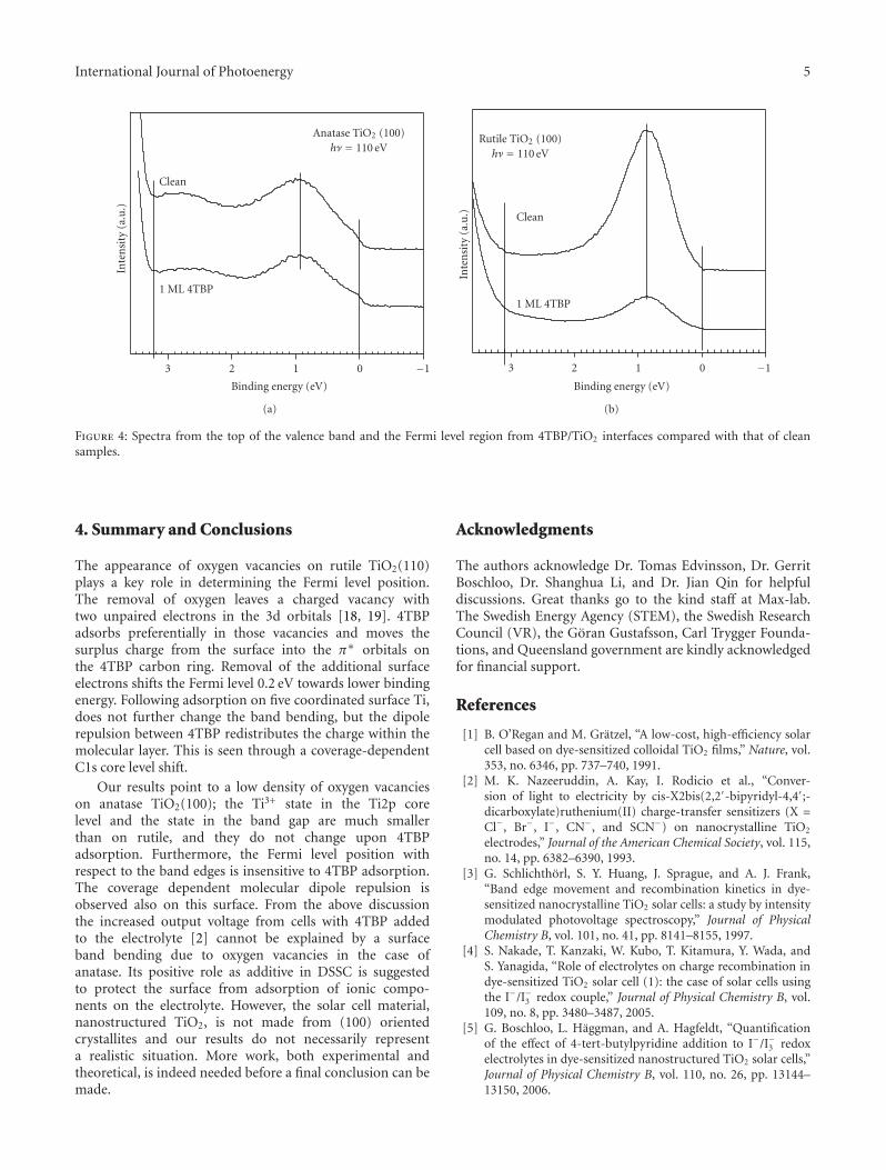
International Journal of Photoenergy 5
Clean
Inte
nsi
ty(a
.u.)
3 2
1 ML 4TBP
1
Binding energy (eV)
0 −1
Anatase TiO2 (100)hν = 110 eV
(a)
Clean
Inte
nsi
ty(a
.u.)
3 2
1 ML 4TBP
1
Binding energy (eV)
0 −1
Rutile TiO2 (100)hν = 110 eV
(b)
Figure 4: Spectra from the top of the valence band and the Fermi level region from 4TBP/TiO2 interfaces compared with that of cleansamples.
4. Summary and Conclusions
The appearance of oxygen vacancies on rutile TiO2(110)plays a key role in determining the Fermi level position.The removal of oxygen leaves a charged vacancy withtwo unpaired electrons in the 3d orbitals [18, 19]. 4TBPadsorbs preferentially in those vacancies and moves thesurplus charge from the surface into the π∗ orbitals onthe 4TBP carbon ring. Removal of the additional surfaceelectrons shifts the Fermi level 0.2 eV towards lower bindingenergy. Following adsorption on five coordinated surface Ti,does not further change the band bending, but the dipolerepulsion between 4TBP redistributes the charge within themolecular layer. This is seen through a coverage-dependentC1s core level shift.
Our results point to a low density of oxygen vacancieson anatase TiO2(100); the Ti3+ state in the Ti2p corelevel and the state in the band gap are much smallerthan on rutile, and they do not change upon 4TBPadsorption. Furthermore, the Fermi level position withrespect to the band edges is insensitive to 4TBP adsorption.The coverage dependent molecular dipole repulsion isobserved also on this surface. From the above discussionthe increased output voltage from cells with 4TBP addedto the electrolyte [2] cannot be explained by a surfaceband bending due to oxygen vacancies in the case ofanatase. Its positive role as additive in DSSC is suggestedto protect the surface from adsorption of ionic compo-nents on the electrolyte. However, the solar cell material,nanostructured TiO2, is not made from (100) orientedcrystallites and our results do not necessarily representa realistic situation. More work, both experimental andtheoretical, is indeed needed before a final conclusion can bemade.
Acknowledgments
The authors acknowledge Dr. Tomas Edvinsson, Dr. GerritBoschloo, Dr. Shanghua Li, and Dr. Jian Qin for helpfuldiscussions. Great thanks go to the kind staff at Max-lab.The Swedish Energy Agency (STEM), the Swedish ResearchCouncil (VR), the Goran Gustafsson, Carl Trygger Founda-tions, and Queensland government are kindly acknowledgedfor financial support.
References
[1] B. O’Regan and M. Gratzel, “A low-cost, high-efficiency solarcell based on dye-sensitized colloidal TiO2 films,” Nature, vol.353, no. 6346, pp. 737–740, 1991.
[2] M. K. Nazeeruddin, A. Kay, I. Rodicio et al., “Conver-sion of light to electricity by cis-X2bis(2,2′-bipyridyl-4,4′;-dicarboxylate)ruthenium(II) charge-transfer sensitizers (X =Cl−, Br−, I−, CN−, and SCN−) on nanocrystalline TiO2
electrodes,” Journal of the American Chemical Society, vol. 115,no. 14, pp. 6382–6390, 1993.
[3] G. Schlichthorl, S. Y. Huang, J. Sprague, and A. J. Frank,“Band edge movement and recombination kinetics in dye-sensitized nanocrystalline TiO2 solar cells: a study by intensitymodulated photovoltage spectroscopy,” Journal of PhysicalChemistry B, vol. 101, no. 41, pp. 8141–8155, 1997.
[4] S. Nakade, T. Kanzaki, W. Kubo, T. Kitamura, Y. Wada, andS. Yanagida, “Role of electrolytes on charge recombination indye-sensitized TiO2 solar cell (1): the case of solar cells usingthe I−/I−3 redox couple,” Journal of Physical Chemistry B, vol.109, no. 8, pp. 3480–3487, 2005.
[5] G. Boschloo, L. Haggman, and A. Hagfeldt, “Quantificationof the effect of 4-tert-butylpyridine addition to I−/I−3 redoxelectrolytes in dye-sensitized nanostructured TiO2 solar cells,”Journal of Physical Chemistry B, vol. 110, no. 26, pp. 13144–13150, 2006.
6 International Journal of Photoenergy
[6] C. Shi, S. Dai, K. Wang, X. Pan, F. Kong, and L. Hu, “Theadsorption of 4-tert-butylpyridine on the nanocrystallineTiO2 and Raman spectra of dye-sensitized solar cells in situ,”Vibrational Spectroscopy, vol. 39, no. 1, pp. 99–105, 2005.
[7] W. Monch, Semiconductor Surface and Interfaces, Springer,Berlin, Germany.
[8] A. L. Linsebigler, G. Lu, and J. T. Yates Jr., “Photocatalysis onTiO2 surfaces: principles, mechanisms, and selected results,”Chemical Reviews, vol. 95, no. 3, pp. 735–758, 1995.
[9] U. Diebold, “The surface science of titanium dioxide,” SurfaceScience Reports, vol. 48, no. 5–8, pp. 53–229, 2003.
[10] E. L. D. Hebenstreit, W. Hebenstreit, H. Geisler et al., “Sulfuron TiO2(110) studied with resonant photoemission,” PhysicalReview B, vol. 64, no. 11, Article ID 115418, pp. 1–11, 2001.
[11] K. E. Smith, J. L. MacKay, and V. E. Henrich, “Interactionof SO2 with nearly perfect and defect TiO2(110) surfaces,”Physical Review B, vol. 35, no. 11, pp. 5822–5829, 1987.
[12] M. Durr, A. Yasuda, and G. Nelles, “On the origin of increasedopen circuit voltage of dye-sensitized solar cells using 4-ferf-butyl pyridine as additive to the electrolyte,” Applied PhysicsLetters, vol. 89, no. 6, Article ID 061110, 2006.
[13] S. Yu, S. Ahmadi, P. Palmgren, F. Hennies, M. Zuleta, and M.Gothelid, “4-tert-butyl pyridine bond site and band bendingon TiO2(110),” Journal of Physical Chemistry C, vol. 114, pp.2315–2320, 2009.
[14] P. Palmgren, B. R. Priya, N. P. P. Niraj, and M. Gothelid,“Bonding of metal-free phthalocyanine to TiO2(110) singlecrystal,” Solar Energy Materials and Solar Cells, vol. 90, no. 20,pp. 3602–3613, 2006.
[15] B.-T. Xiong, B.-X. Zhou, Z.-Y. Zhu et al., “Adsorption of4-tert-butylpyridine on TiO2 surface in dye-sensitized solarcells,” Chinese Journal of Chemistry, vol. 26, no. 1, pp. 70–76,2008.
[16] C. M. Yim, C. L. Pang, and G. Thornton, “Oxygen vacancyorigin of the surface band-gap state of TiO2(110),” PhysicalReview Letters, vol. 104, no. 3, Article ID 036806, 2010.
[17] S. Wendt, P. T. Sprunger, E. Lira et al., “The role of interstitialsites in the Ti3d defect state in the band gap of titania,” Science,vol. 320, no. 5884, pp. 1755–1759, 2008.
[18] T. Bredow and G. Pacchioni, “Electronic structure of anisolated oxygen vacancy at the TiO2(1 1 0) surface,” ChemicalPhysics Letters, vol. 355, no. 5-6, pp. 417–423, 2002.
[19] B. J. Morgan and G. W. Watson, “A DFT + U description ofoxygen vacancies at the TiO2 rutile (1 1 0) surface,” SurfaceScience, vol. 601, no. 21, pp. 5034–5041, 2007.
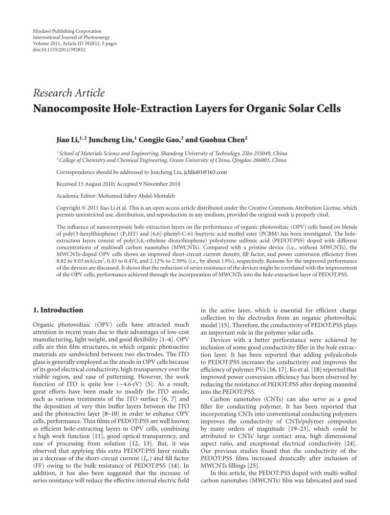
Hindawi Publishing CorporationInternational Journal of PhotoenergyVolume 2011, Article ID 392832, 5 pagesdoi:10.1155/2011/392832
Research Article
Nanocomposite Hole-Extraction Layers for Organic Solar Cells
Jiao Li,1, 2 Juncheng Liu,1 Congjie Gao,2 and Guohua Chen2
1 School of Materials Science and Engineering, Shandong University of Technology, Zibo 255049, China2 College of Chemistry and Chemical Engineering, Ocean University of China, Qingdao 266003, China
Correspondence should be addressed to Juncheng Liu, [email protected]
Received 15 August 2010; Accepted 9 November 2010
Academic Editor: Mohamed Sabry Abdel-Mottaleb
Copyright © 2011 Jiao Li et al. This is an open access article distributed under the Creative Commons Attribution License, whichpermits unrestricted use, distribution, and reproduction in any medium, provided the original work is properly cited.
The influence of nanocomposite hole-extraction layers on the performance of organic photovoltaic (OPV) cells based on blendsof poly(3-hexylthiophene) (P3HT) and [6,6]-phenyl-C-61-buytyric acid methyl ester (PCBM) has been investigated. The hole-extraction layers consist of poly(3,4,-ethylene dioxythiophene) polystyrene sulfonic acid (PEDOT:PSS) doped with differentconcentrations of multiwall carbon nanotubes (MWCNTs). Compared with a pristine device (i.e., without MWCNTs), theMWCNTs-doped OPV cells shows an improved short-circuit current density, fill factor, and power conversion efficiency from8.82 to 9.03 mA/cm2, 0.43 to 0.474, and 2.12% to 2.39% (i.e., by about 13%), respectively. Reasons for the improved performanceof the devices are discussed. It shows that the reduction of series resistance of the devices might be correlated with the improvementof the OPV cells, performance achieved through the incorporation of MWCNTs into the hole-extraction layer of PEDOT:PSS.
1. Introduction
Organic photovoltaic (OPV) cells have attracted muchattention in recent years due to their advantages of low-costmanufacturing, light weight, and good flexibility [1–4]. OPVcells are thin film structures, in which organic photoactivematerials are sandwiched between two electrodes. The ITOglass is generally employed as the anode in OPV cells becauseof its good electrical conductivity, high transparency over thevisible region, and ease of patterning. However, the workfunction of ITO is quite low (∼4.6 eV) [5]. As a result,great efforts have been made to modify the ITO anode,such as various treatments of the ITO surface [6, 7] andthe deposition of very thin buffer layers between the ITOand the photoactive layer [8–10] in order to enhance OPVcells, performance. Thin films of PEDOT:PSS are well knownas efficient hole-extracting layers in OPV cells, combininga high work function [11], good optical transparency, andease of processing from solution [12, 13]. But, it wasobserved that applying this extra PEDOT:PSS layer resultsin a decrease of the short-circuit current (Isc) and fill factor(FF) owing to the bulk resistance of PEDOT:PSS [14]. Inaddition, it has also been suggested that the increase ofseries resistance will reduce the effective internal electric field
in the active layer, which is essential for efficient chargecollection to the electrodes from an organic photovoltaicmodel [15]. Therefore, the conductivity of PEDOT:PSS playsan important role in the polymer solar cells.
Devices with a better performance were achieved byinclusion of some good conductivity filler in the hole extrac-tion layer. It has been reported that adding polyalcoholsto PEDOT:PSS increases the conductivity and improves theefficiency of polymer PVs [16, 17]. Ko et al. [18] reported thatimproved power conversion efficiency has been observed byreducing the resistance of PEDOT:PSS after doping mannitolinto the PEDOT:PSS.
Carbon nanotubes (CNTs) can also serve as a goodfiller for conducting polymer. It has been reported thatincorporating CNTs into conventional conducting polymersimproves the conductivity of CNTs/polymer compositesby many orders of magnitude [19–23], which could beattributed to CNTs’ large contact area, high dimensionalaspect ratio, and exceptional electrical conductivity [24].Our previous studies found that the conductivity of thePEDOT:PSS films increased drastically after inclusion ofMWCNTs fillings [25].
In this article, the PEDOT:PSS doped with multi-walledcarbon nanotubes (MWCNTs) film was fabricated and used
2 International Journal of Photoenergy
Aluminum
Active layer(P3HT:PCBM)
Hole-extraction layer(MWCNTs-PEODT:PSS)
ITO
Glass
− +
Figure 1: Schematic device structure for organic solar cells dopedwith MWCNTs.
as hole-extraction layer for OPV cells. The effect of MWCNTsconcentration on the photovoltaic performance of the devicebased on P3HT:PCBM blend was investigated. Reasons forthe improved performance of the devices were also discussed.
2. Experimental
Multi-walled carbon nanotubes (MWCNTs) (diameter: 10∼30 nm, length: 5∼15 μm, purity:>95%) were purchased fromBeijing Nachen Nanotech Co. Ltd., and the MWCNTs werefurther purified with strong acid. In a typical procedure,30 mg of MWCNTs was added into an acid solution ofconcentrated sulphuric acid (15 mL) and concentrated nitricacid (5 mL). The mixture was ultrasonicated for 20 minutes,stirred for 1 hour in reflux at 130◦C, vacuum filtered througha 0.2 μm milli-pore polycarbonate membrane, washed withexcess-distilled water until the pH 7.0, and filtrated thendried under vacuum for 12 h at 60◦C.
PEDOT:PSS aqueous solution (1.3 wt% dispersed inH2O) from Aldrich (as supplied) was filtered with a 0.45 μmpolyvinyl difluoride (PVDF) syringe filter. Some amountof acid-treated MWCNTs were added into the PEDOT:PSSsolution to form the nanocomposites. The composites weretreated in ultrasonic bath for about 12 hours before using forspin coating.
All the devices in this work were fabricated using indium-tin-oxide- (ITO-) coated glass substrates (<10Ω/�). TheITO substrates were ultrasonically cleaned with a seriesof organic solvents (ethanol, methanol, and acetone), thenrinsed in ultrasonic bath with deionized water and driedin a vacuum oven. Residual organic contaminations weresubsequently removed by exposing to a UV-ozone lamp for30 min. Nanocomposites of MWCNTs and PEDOT:PSS werespin coated on top of the ITO surface to form an (90–100 nm) layer before drying the substrates at 120◦C in anoven for more than 30 min. The P3HT:PCBM was dissolvedin dichlorobenzene at a weight ratio of 1 : 0.8 and stirred formore than 72 h in the glovebox before spin casting to formthe blend layer. Finally an Al electrode of about 100 nm inthickness was deposited by thermal evaporation at a pressureof 2.4 × 10⁻⁴ Pa through a shadow mask. No buffer layerbetween the organic layer and cathode is used. The basicstructure of the OPV devices is shown in Figure 1.
The surface morphology of MWCNTs was carried out byfield emission scanning electron microscopy (FESEM, JEOL,
JSM-6335 F). The optical property of the composite filmswas characterized with a TU-1901 Dual-beam UV-Visiblespectrophotometer. Current density-voltage (I-V) charac-teristics of the PV cells were measured using a computer-controlled Keithley 2400 Source Meter in the dark and undera simulated light intensity of 100 mW/cm2 (AM 1.5 G)calibrated by an optical power meter from a halogen lamp.The power conversion efficiency (PCE) was calculated fromthe I-V characteristics. The devices were tested in air withoutencapsulation.
3. Results and Discussion
Figure 2. compares the surface morphology of the MWCNTsbefore acid treatment (Figure 2(a)) and after acid treatment(Figure 2(b)). It can be see that particle-like impurity ofMWCNTs is removed and the morphology, as in termsof the surface smoothness, is improved after the acidtreatment. Moreover, the MWCNTs after acid treatmentcan be dispersed into aqueous PEDOT:PSS solution and noprecipitation is observed in the solution after several weeks.
The transmittance of the nanocomposites is shown inFigure 3. The pristine PEDOT:PSS film gives a good opticaltransmittance (93.2% average) on the wavelength range from550 nm to 950 nm, which corresponds to the power densityof ambient sunlight on the Earth’s surface [26]. However, thetransmittance of PEDOT : PSS film decreases with increasingamount of MWCNTs. With the MWCNTs concentrationincreasing to 0.20 wt%, the transmittance of composite filmdropped by 7.5% (86.2% average). This may result from theformation of the conductive network of MWCNTs and someabsorptions of MWCNTs in the above wavelength range[27, 28].
Solar cells generally have a series resistance and shuntresistance associated with them. In practice, a high shuntresistance and a low series resistance are required simul-taneously for an ideal photovoltaic device [29]. The shuntresistance usually reflects the degree of leakage currentthrough the device, which relates to the overall quality ofthe films. Meanwhile, the series resistance is attributed to theohmic loss in the whole device, which includes the resistanceof the active layer, metal-organic contacts, the electrodes, andthe conductivity of the hole-extraction layer [30].
The influence of the doping on the shunt resistance ofthe device can be observed in the I-V curves under lower biasin the dark. As appeared in Figure 4, at reverse negative biasand at the linear regime of forward bias, where the currentis limited by shunt resistance due to the leakage current, thecurrent gradually increases with the dopant concentration.The increasing current with doping concentration may beinduced by random leakage current in higher conductivityM-PEDOT:PSS layer. Some phase separation and moredefects caused by MWCNTs-doping in the PEDOT:PSS mayhave induced some leakage current through the device.
Figure 5 shows the current density-voltage curves ofphotovoltaic cells with different doping concentrations ofMWCNTs in the PEDOT:PSS. The detailed parameters ofdevices are summarized in Table 1.

International Journal of Photoenergy 3
Acc. V10 kV
Spot
3
Magn
50000xDetTLD
WD5.2
500 nmFEI Sirion200 SEM
(a)
Acc. V10 kV
Spot
3
Magn
50000x
DetTLD
500 nmFEI Sirion200 SEM
WD4.9
(b)
Figure 2: SEM of untreated and treated MWCNTs- (a) untreated MWCNTs; (b) treated MWCNTs
Table 1: PV parameters of OPVs for MWCNTs doping.
Style Structure Voc (V) Isc (mA/cm2) FF (%) η (%)
A ITO/PEDOT:PSS/P3HT:PCBM/Al 0.56 8.82 43.0 2.12%
B ITO/M (0.04 wt%)-PEDOT:PSS/P3HT:PCBM/Al 0.56 9.03 47.4 2.39%
C ITO/M (0.10 wt%)-PEDOT:PSS/P3HT:PCBM/Al 0.55 9.52 44.8 2.35%
D ITO/M (0.20 wt%)-PEDOT:PSS/P3HT:PCBM/Al 0.55 9.34 43.4 2.22%
0
10
20
30
40
50
60
70
80
90
100
110
Tran
smit
tan
ce(%
)
Wavelength (nm)
a b
cd
550 600 650 700 750 800 850
a: PEDOT:PSSb: M (0.04 wt%)-PEDOT:PSS
c: M (0.1 wt%)-PEDOT:PSSd: M (0.2 wt%)-PEDOT:PSS
Figure 3: The optical transmittance of films as a function of weightfraction of MWCNTs.
A small change in Voc with increase in MWCNTs amountwas observed as shown in Table 1, where the values slightlyvary around 0.56 V. It was found that the open circuit voltageof the solar cell correlates directly with the work function ofthe electrodes or the buffer layers, that is, it is determinedby the work function of PEDOT:PSS film [14, 17]. So the
−2 −1 0 1 2
1000
100
10
1
0.1
0.01
1E− 3
1E− 4
1E− 5
1E− 6
Voltage (V)
Cu
rren
tde
nsi
ty(m
A/c
m2)
Device ADevice B
Device CDevice D
Figure 4: The dark I-V characteristics of devices with differentconcentrations of MWCNTs. Device A: pristine PEDOT:PSS film;Device B: M (0.04 wt%)-PEDOT:PSS film; Device C: M (0.10 wt%)-PEDOT:PSS film; Device D: M (0.20 wt%)-PEDOT:PSS film.
addition of MWCNTs into PEDOT:PSS may not affect thework functions of PEDOT:PSS films in the solar cell.
Table 1 also shows the increase in Isc from about8.82 mA/cm2 of the reference device A (0 wt% doping) to

4 International Journal of Photoenergy
Device ADevice B
Device CDevice D
−10
−8
−6
−4
−2
0
0.2 0.4 0.6 0.8
2
0
Voltage (V)
Cu
rren
tde
nsi
ty(m
A/c
m2)
Figure 5: The I-V characteristics of devices with different con-centrations of MWCNTs. Device A: pristine PEDOT:PSS film;Device B: M (0.04 wt%)-PEDOT:PSS film; Device C: M (0.10 wt%)-PEDOT:PSS film; Device D: M(0.20 wt%)-PEDOT:PSS film.
9.52 mA/cm2 of the device C (0.10 wt% doping), and afterthat the Isc decreases to become 9.34 mA/cm2 of the deviceD (0.20 wt% doping). Since these devices are fabricated withthe same materials and the same procedure, and the onlydifference is the hole-extraction layer, the increased currentis unlikely on account of other reasons, but due to the highconductivity of the composite hole-extraction layers, leadingto a lower series resistance of the device. The generatedhole carriers in the P3HT:PCBM active layer easily moveinto the anode through the MWCNTs-doped PEDOT:PSSlayer. While the decrease in Isc after adding more amount ofMWCNTs may be due to the decrease of the transmittanceof composite films in the wavelength around of 700 nm(as shown in Figure 3), which has effects on the photonabsorption yield and the charge-carrier-transport yield ofthe PV cells [26]. The lowering of serial resistivity in hole-extraction layers with increased MWCNT concentration isalso responsible for increase in the fill factor from 0.43to 0.474. But as shown in Figure 4, extra amounts of theMWCNTs tend to decrease the OPV cells, shunt resistance,which can affect fill factor of OPV cells [29, 31]. Then lowerfill factor is obtained in device C and device D.
The enhancement in both Isc and FF by introducingMWCNTs into solar cell structure tends to cause improve-ment in the power conversion efficiency from 2.12% to2.39%, that is, by about 13%.
4. Conclusion
In summary, We developed efficient OPV cells based onP3HT:PCBM blend by incorporating MWCNTs into hole-extraction layer of PEDOT:PSS. Compared with the pristineOPV device without adding MWCNTs to the hole-extraction
layer, the MWCNTs-doped OPV cells show an improvedshort-circuit current density, fill factor, and power conver-sion efficiency from 8.82 to 9.03 mA/cm2, 0.43 to 0.474,and 2.12% to 2.39% (i.e., by about 13%), respectively. Thehigh electrical conductivity properties of the composite filmsmight contribute to facility the hole-extraction and hole-transport ability of PEDOT:PSS, which leads to the reductionof series resistance of the devices.
Acknowledgment
Financial support from the program for New CenturyExcellent Talents in University (NCET, Grant no. NCET-04-0648) is gratefully acknowledged.
References
[1] T. D. Nielsen, C. Cruickshank, S. Foged, J. Thorsen, and F. C.Krebs, “Business, market and intellectual property analysis ofpolymer solar cells,” Solar Energy Materials and Solar Cells, vol.94, no. 10, pp. 1553–1571, 2010.
[2] B. Kippelen and J. L. Bredas, “Organic photovoltaics,” Energyand Environmental Science, vol. 2, no. 3, pp. 251–261, 2009.
[3] M. Helgesen, R. Søndergaard, and F. C. Krebs, “Advancedmaterials and processes for polymer solar cell devices,” Journalof Materials Chemistry, vol. 20, no. 1, pp. 36–60, 2010.
[4] F. C. Krebs, “Fabrication and processing of polymer solar cells:a review of printing and coating techniques,” Solar EnergyMaterials and Solar Cells, vol. 93, no. 4, pp. 394–412, 2009.
[5] D. Y. Kim, F. So, and Y. Gao, “Aluminum phthalocyaninechloride/C organic photovoltaic cells with high open-circuitvoltages,” Solar Energy Materials and Solar Cells, vol. 93, no. 9,pp. 1688–1691, 2009.
[6] J. S. Kim, J. H. Park, J. H. Lee, J. Jo, D. Y. Kim, and K.Cho, “Control of the electrode work function and active layermorphology via surface modification of indium tin oxide forhigh efficiency organic photovoltaics,” Applied Physics Letters,vol. 91, no. 11, pp. 2111–2113, 2007.
[7] C. C. Wu, C. I. Wu, J. C. Sturm, and A. Kahn, “Surfacemodification of indium tin oxide by plasma treatment: aneffective method to improve the efficiency, brightness, andreliability of organic light emitting devices,” Applied PhysicsLetters, vol. 70, no. 11, pp. 1348–1350, 1997.
[8] F. Liu, S. Shao, X. Guo, Y. Zhao, and Z. Xie, “Efficient polymerphotovoltaic cells using solution-processed MoO3 as anodebuffer layer,” Solar Energy Materials and Solar Cells, vol. 94,no. 5, pp. 842–845, 2010.
[9] S. W. Tong, C. F. Zhang, C. Y. Jiang et al., “Improvementin the hole collection of polymer solar cells by utilizing goldnanoparticle buffer layer,” Chemical Physics Letters, vol. 453,no. 1–3, pp. 73–76, 2008.
[10] R. A. Hatton, N. P. Blanchard, LI. W. Tan, G. Latini, F. Cacialli,and S. R. P. Silva, “Oxidised carbon nanotubes as solutionprocessable, high work function hole-extraction layers fororganic solar cells,” Organic Electronics, vol. 10, no. 3, pp. 388–395, 2009.
[11] T. M. Brown, J. S. Kim, R. H. Friend, F. Cacialli, R.Daik, and W. J. Feast, “Built-in field electroabsorptionspectroscopy of polymer light-emitting diodes incorporatinga doped poly(3,4-ethylene dioxythiophene) hole injectionlayer,” Applied Physics Letters, vol. 75, no. 12, pp. 1679–1681,1999.
International Journal of Photoenergy 5
[12] G. Heywang and F. Jonas, “Poly(alkylenedioxythiophene)s—new, very stable conducting polymers,” Advanced Materials,vol. 4, no. 2, pp. 116–118, 1992.
[13] L. Groenendaal, F. Jonas, D. Freitag, H. Pielartzik, andJ. R. Reynolds, “Poly(3,4-ethylenedioxythiophene) and itsderivatives: past, present, and future,” Advanced Materials, vol.12, no. 7, pp. 481–494, 2000.
[14] T. Aernouts, W. Geens, J. Poortmans, P. Heremans, S. Borghs,and R. Mertens, “Extraction of bulk and contact componentsof the series resistance in organic bulk donor-acceptor-heterojunctions,” Thin Solid Films, vol. 403-404, pp. 297–301,2002.
[15] B. Mazhari, “An improved solar cell circuit model for organicsolar cells,” Solar Energy Materials and Solar Cells, vol. 90, no.7-8, pp. 1021–1033, 2006.
[16] F. Zhang, M. Johansson, M. R. Andersson, J. C. Hummelen,and O. Inganas, “Polymer photovoltaic cells with conductingpolymer anodes,” Advanced Materials, vol. 14, no. 9, pp. 662–665, 2002.
[17] F. L. Zhang, A. Gadisa, O. Inganas, M. Svensson, and M. R.Andersson, “Influence of buffer layers on the performance ofpolymer solar cells,” Applied Physics Letters, vol. 84, no. 19, pp.3906–3908, 2004.
[18] C. J. Ko, YI. K. Lin, F. C. Chen, and C. W. Chu, “Modifiedbuffer layers for polymer photovoltaic devices,” Applied PhysicsLetters, vol. 90, no. 6, Article ID 063509, 2007.
[19] H. Peng and X. Sun, “Highly aligned carbonnanotube/polymer composites with much improved electricalconductivities,” Chemical Physics Letters, vol. 471, no. 1–3, pp.103–105, 2009.
[20] Z. Yang, H. Pu, J. Yuan, D. Wan, and Y. Liu, “Phthalocyanines-MWCNT hybrid materials: fabrication, aggregation and pho-toconductivity properties improvement,” Chemical PhysicsLetters, vol. 465, no. 1–3, pp. 73–77, 2008.
[21] M. C. Wu, Y. Y. Lin, S. Chen et al., “Enhancing light absorptionand carrier transport of P3HT by doping multi-wall carbonnanotubes,” Chemical Physics Letters, vol. 468, no. 1–3, pp. 64–68, 2009.
[22] K. R. Reddy, B. C. Sin, K. S. Ryu, J. C. Kim, H. Chung,and Y. Lee, “Conducting polymer functionalized multi-walledcarbon nanotubes with noble metal nanoparticles: synthesis,morphological characteristics and electrical properties,” Syn-thetic Metals, vol. 159, no. 7-8, pp. 595–603, 2009.
[23] T. M. Wu, H. L. Chang, and Y. W. Lin, “Synthesis and char-acterization of conductive polypyrrole/multi-walled carbonnanotubes composites with improved solubility and conduc-tivity,” Composites Science and Technology, vol. 69, no. 5, pp.639–644, 2009.
[24] R. H. Baughman, A. A. Zakhidov, and W. A. De Heer, “Carbonnanotubes—the route toward applications,” Science, vol. 297,no. 5582, pp. 787–792, 2002.
[25] C. Gao, J. Li, J. Liu, J. Zhang, and H. Sun, “Influenceof MWCNTs doping on the structure and properties ofPEDOT:PSS films,” International Journal of Photoenergy, vol.2009, Article ID 650509, 5 pages, 2009.
[26] B. R. Saunders and M. L. Turner, “Nanoparticle-polymerphotovoltaic cells,” Advances in Colloid and Interface Science,vol. 138, no. 1, pp. 1–23, 2008.
[27] S. Ghosh and O. Inganas, “Self-assembly of a conductingpolymer nanostructure by physical crosslinking: applicationsto conducting blends and modified electrodes,” SyntheticMetals, vol. 101, no. 1–3, pp. 413–416, 1999.
[28] J. K. W. Sandler, J. E. Kirk, I. A. Kinloch, M. S. P. Shaffer, andA. H. Windle, “Ultra-low electrical percolation threshold in
carbon-nanotube-epoxy composites,” Polymer, vol. 44, no. 19,pp. 5893–5899, 2003.
[29] H. Z. Yu and J. B. Peng, “Influence of the solvent and devicestructure on the performance of the MEH-PPV:PCBM solarcell,” Acta Physico—Chimica Sinica, vol. 23, no. 10, pp. 1637–1641, 2007 (Chinese).
[30] J. Xue, S. Uchida, B. P. Rand, and S. R. Forrest, “4.2% efficientorganic photovoltaic cells with low series resistances,” AppliedPhysics Letters, vol. 84, no. 16, pp. 3013–3015, 2004.
[31] D. Gupta, S. Mukhopadhyay, and K. S. Narayan, “Fill factor inorganic solar cells,” Solar Energy Materials and Solar Cells, vol.94, no. 8, pp. 1309–1313, 2010.
Hindawi Publishing CorporationInternational Journal of PhotoenergyVolume 2011, Article ID 340540, 4 pagesdoi:10.1155/2011/340540
Research Article
Nanostructural Materials for Energy Storage Systems
Bronislaw Buczek
Faculty of Energy and Fuels, AGH University of Science and Technology, 30 Mickiewicza Avenue, 30-059 Cracow, Poland
Correspondence should be addressed to Bronislaw Buczek, [email protected]
Received 31 August 2010; Revised 9 November 2010; Accepted 24 December 2010
Academic Editor: Mohamed Sabry Abdel-Mottaleb
Copyright © 2011 Bronislaw Buczek. This is an open access article distributed under the Creative Commons Attribution License,which permits unrestricted use, distribution, and reproduction in any medium, provided the original work is properly cited.
The aim of this study was to assess of carbonaceous monoliths used for adsorption cooling systems. The carbonaceous monolithsprepared from coal precursors are obtained. The porous structure of monoliths was evaluated on the basis of nitrogen adsorption-desorption data. The investigated monoliths have significantly developed microporous structure. The large specific area ofcarbonaceous monoliths (about 2000 m2/g) and volume of micropores are observed. Methanol adsorption isotherms and heatof wetting using methanol was determined. Results show that monoliths materials are high adsorption capacity of methanol andheat of wetting, which can improve of heat exchange and efficiency in processes of refrigeration and air conditioning.
1. Introduction
Processes of mass and energy storage with application ofmicroporous adsorbent can be included into prospectivedirections of the adsorption technology development. Theapplication of carbonaceous adsorbents for heat storagecan be used in adsorptive refrigerators utilizing closedthermodynamic cycles [1]. The most interesting system ismethyl alcohol and microporous carbon material pair [2].Because of its ability to selectively adsorb vapours andgases, extended internal porosity, and large specific surfacearea, active carbon is a good adsorbent for storage of massand energy [3]. Methanol is more easily desorbed, and itsworking pressure is always lower than atmospheric pressure,which allows for a rapid identification of any faults in acooling system. The temperature of desorption of methanolfrom an adsorbent is considerably lower than for watervapour systems. For all these reasons the methanol-activecarbon pair can be used for mass and energy storage.
The wide developing techniques of solar heating with useof different types of solar collectors found the use also inadsorption cooling system. The adsorption cooling systemwith solar collector was presented in Figure 1.
The performance of an adsorbent in a thermodynamicsystem depends upon properties such as specific area, typeand number of pores, adsorbent form, and adsorption
enthalpy of the adsorbate and its thermal conductivity.Therefore, any method of modification of active carbon hasto improve carbon structural features and to increase the heatand mass transfer [4].
The good adsorbent should have not only developedmicroporous structure but also large bulk density, whichimprove packing and heat conductivity on adsorbent bed[5]. It depends on shape of adsorbent: powder, granular,or disk monolith [6, 7]. We can increase the packing up ofthe particles in order to prepare microporous monoliths andsimultaneously to increase heat conductivity of its bed.
Active carbon-methanol pair appears to be suitablefor different adsorptive cooling systems. This pair can besuccessfully used as fridge for storage of food and medicinesand ice manufacture, in air conditioning devices and heatpumps [8].
2. Experimental and Results
Investigations were carried on four carbonaceous monoliths.The aim of this study was to assess the monoliths used foradsorption cooling systems. The carbonaceous monolithsprepared from hard coal precursors are obtained fromFaculty of Chemistry, Wroclaw University of Technology [9].Preparations of carbon monoliths are presented in Figure 2.
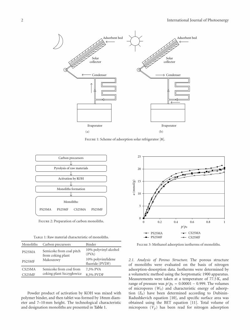
2 International Journal of Photoenergy
Adsorbent bed
Solarcollector
Condenser
Evaporator
(a)
Adsorbent bed
Solarcollector
Condenser
Evaporator
(b)
Figure 1: Scheme of adsorption solar refrigerator [8].
Carbon precursors
Pyrolysis of raw materials
Activation by KOH
Monoliths formation
Monoliths:
PS25MA PS25MF CS25MA PS25MF
Figure 2: Preparation of carbon monoliths.
Table 1: Raw material characteristic of monoliths.
Monoliths Carbon precursors Binder
PS25MA Semicoke from coal pitchfrom coking plantMakoszowy
10% polyvinyl alcohol(PVA)
PS25MF10% polyvinylidenefluoride (PVDF)
CS25MA Semicoke from coal fromcoking plant Szczygłowice
7,5% PVA
CS25MF 8,5% PVDF
Powder product of activation by KOH was mixed withpolymer binder, and then tablet was formed by 18mm diam-eter and 7–10 mm height. The technological characteristicand designation monoliths are presented in Table 1.
0
5
10
15
20
25
0 0.2 0.4 0.6 0.8 1
p/p0
a(m
mol
/g)
PS25MAPS25MF
CS25MACS25MF
Figure 3: Methanol adsorption isotherms of monoliths.
2.1. Analysis of Porous Structure. The porous structureof monoliths were evaluated on the basis of nitrogenadsorption-desorption data. Isotherms were determined bya volumetric method using the Sorptomatic 1900 apparatus.Measurements were taken at a temperature of 77.5 K, andrange of pressure was p/p0 = 0.00001− 0.999. The volumesof micropores (W0) and characteristic energy of adsorp-tion (E0) have been determined according to Dubinin-Radushkevich equation [10], and specific surface area wasobtained using the BET equation [11]. Total volume ofmicropores (Vp) has been read for nitrogen adsorption

International Journal of Photoenergy 3
1
2
3
4
5
6
K1
K2K3 K4K5
Figure 4: Scheme of equipment for measuring the heat of wetting:1-calorimetric cell, 2-container of methanol, 3-electronic system totemperature measurement, 4-vacuum pump, 5-control vessel, 6-filter.
Table 2: Structural properties of monoliths.
Monolith W0 cm3/g E0 kJ/mol SBET m2/g Vp cm3/g
PS25MA 0.714 18.3 1910 0.925
PS25MF 0.672 18.1 1830 0.887
CS25MA 0.709 18.4 1880 0.876
CS25MF 0.689 18.4 1805 0.854
isotherms of value p/p0 = 0.99. The results of calculationsare shown in Table 2.
The carbonaceous monoliths are characterized by sig-nificantly developed microporous structure. They achieveda large volume of micropores (0.672–0.714 cm3/g) andvery impressive specific surface area (1805–1910 m2/g). Thebiggest microporous structure for monoliths formed withpolyvinyl alcohol (PVA) is observed.
2.2. Methanol Adsorption. Methanol adsorption isotherms ofmonoliths were measured volumetrically. The measurementswere carried out in the temperature 298 K.
The adsorption isotherms of methanol vapours formonoliths are presented in Figure 3.
All of the samples readily adsorb methanol givingreversible isotherms of type I. Adsorption capacity decreasessimultaneously when the temperature rises. It is charac-teristic for highly microporous adsorbent. The investigatedmonoliths have related structural proprieties, and the courseof isotherms is very similar in whole range of pressures. Themonolith PS25MA characterizes insensibly larger adsorptive
Table 3: Heat effect and heat of wetting of monoliths.
Monoliths ΔT Q, J/g dT/dt
PS25MA 7.6 159.83 177.0
PS25MF 5.3 111.03 331.2
CS25MA 7.9 165.14 35.9
CS25MF 7.6 160.43 119.8
capacity. It can be noticed also that larger methanol adsorp-tive capacity for monoliths with PVA as binder is observed.
2.3. Heat Effects. The important factor of designing systemsof adsorptive refrigerating, decisive for their performance,is the thermal effects of the process. Energetic effectsof adsorption can be directly determined by calorimetricmeasurements. They can also be estimated by computingmethods from the adsorption isotherms measured at varioustemperatures (the isosteric heat of adsorption).
For the estimation of the energetic effects characterizingthe investigated monoliths, the heat of their wetting bymethanol has been determined. The heat of wetting, evolvedas a result of the mutual interaction of the molecules of thewetting liquid and the adsorbent surface, is a valuable sourceof information. The measurements of the heat of wettingwere carried out in the original apparatus, which is presentedin Figure 4 [12].
For the estimation of the energetic effects characterizingthe investigated monoliths, the heat of their wetting bymethanol has been determined. The values of the heat ofwetting Q, the values of the temperature increase ΔT, dT/dtare collected in Table 3.
Monoliths were characterized by significantly great ener-getic effects related to the heat of wetting with methanol.Heat effects and determined heat of wetting for monolithsare very high. The largest thermal effect (165,14 J/g) as wellas the quickest increase of temperature (dT/dt = 35, 9) wasnoted down for monolith CS25MA. For monoliths what usepolivinyl alcohol as binder (PS25MA, CS25MA) the largerheat of wetting than monoliths with polyvinylidene fluoride(PS25MF, CS25MF) is observed.
3. Conclusion
In this study, the porous structure of monoliths was analysed,and adsorption equilibrium and heat effects of wettingby methanol have been determined. We could evaluate ofcarbon monoliths used for adsorption cooling system.
Pyrolysis of raw materials (carbon precursors), activationby KOH, and monoliths formation give us very attractivematerials as an adsorbent for energy storage systems. Theinvestigated monoliths have significantly developed micro-porous structure. The large specific area of carbonaceousmonoliths (about 2000 m2/g) and volume of micropores areobserved. The methanol adsorptive capacity of all monolithsis also impressive.
Experimental results show that carbon monoliths mate-rials have very high adsorption capacity of methanol and heat
4 International Journal of Photoenergy
of wetting, which can improve heat exchange and efficiencyin processes of cooling and air conditioning.
The carbonaceous monoliths are also characterized bylarge energetic effects related to the heat of wetting withmethanol. All these advantages improve the performance andefficiency of the system in adsorptive refrigeration.
Acknowledgment
The authors are grateful to AGH (Project no. 11.11.210.125)for its financial support of this work.
References
[1] F. Meunier, “Adsorptive cooling: a clean technology,” CleanProducts and Processes, vol. 3, no. 1, pp. 8–20, 2001.
[2] A. P. F. Leite, M. B. Grilo, R. R. D. Andrade, F. A. Belo, and F.Meunier, “Experimental evaluation of a multi-tubular adsor-ber operating with activated carbon-methanol,” Adsorption,vol. 11, no. 1, pp. 543–548, 2005.
[3] H. Marsh and F. Rodriguez-Reinoso, Activated Carbon, Else-vier, 2006.
[4] B. Buczek and E. Wolak, “Nanostructural active carbons fromvegetable precursors for heat storage system,” Chemical andProcess Engineering, vol. 30, no. 1, pp. 173–180, 2009.
[5] G. Cacciola, G. Restuccia, and L. Mercadante, “Compositesof activated carbon for refrigeration adsorption machines,”Carbon, vol. 33, no. 9, pp. 1205–1210, 1995.
[6] B. S. Akkimaradi, M. Prasad, P. Dutta, and K. Srinivasan,“Effect of packing density and adsorption parameters on thethroughput of a thermal compressor,” Carbon, vol. 40, no. 15,pp. 2855–2859, 2002.
[7] J. Walendziejewski and J. Trawczynski, “Wplyw ksztaltu ziarnakatalizatora HDS na jego wlasciwosci fizykochemiczne iaktywnosc hydroodsiarczajaca,” Przem Chem, vol. 74, p. 138,1993.
[8] E. Wolak and B. Buczek, “Kierunki badan i praktycznychzastosowan układu wegiel aktywny-metanol,” Inzynieria iAparatura Chemiczna, vol. 6, pp. 11–16, 2005 (Polish).
[9] K. Kierzek, H. Machnikowska, G. Gryglewicz, and J. Mach-nikowski, “Methane storage capacity of monoliths madeof activated carbons of different porosity development,” inProceedings of the International Conference on Coal Science andTechnology (ICC&T ’07), Nottingham, UK, August 2007, (CD-ROM).
[10] M. M. Dubinin, “Adsorption properties and microporousstructures of carbonaceous adsorbents,” Carbon, vol. 25, no.5, pp. 593–598, 1987.
[11] R. M. A. Roque-Malherbe, Adsorption and Diffusion inNanoporous Materials, CRC Press, Taylor & Francis, BocaRaton, Fla, USA, 2007.
[12] B. Buczek and E. Wolak, “Potassium hydroxide modified activecarbon for adsorptive refrigerators,” Adsorption, vol. 14, no. 2-3, pp. 283–287, 2008.