nanotechnology in the sbir/sttr ptnsfprograms at nsf
TRANSCRIPT

Nanotechnology in the SBIR/STTR P t NSFPrograms at NSF
T. James RuddGrace J. Wang
Ben SchragBen Schrag
Industrial Innovation and Partnerships Division Engineering Directorate
National Science Foundation
Nanoscale Science and Engineering Grantees Conference National Science Foundation
Arlington , VADecember 7th, 2010

SBIR/STTR Funding Criteria
Project must be innovative
Must demonstrate high commercial potential and /or societal benefit
SBIR program supports high risk* component
2
* From the market viewpoint

NSF SBIR/STTR Innovation Model
Phase IIBThird-Party
Investment + Private Sector or
Non-SBIR Phase I B
1:2 NSF
MATCHMAKER
1:2 NSF Matching
Investment1:2 NSF
Matching
PHASE IIIProduct
Development toC i l
PHASE IFeasibilityResearch
$150k/6
PHASE IIResearchtowards
Prototype CommercialMarket
$150k/6 mos Prototype$500k/24 mos
TaxesFederalFederal Investment

Technologies Supported in SBIR/STTR Program at NSF
Nanotechnology Advanced Materials &Nanotechnology, Advanced Materials & ManufacturingBi t h l d Ch i lBiotechnology and Chemical Technologies
Information and Communication Technologies
Education Applications

Nanotechnology Thrusts in SBIR/STTR at NSFat NSF Nanomaterials
Nanomanufacturing
Nanoelectronics and Active Nanostructures
Nanotechnology for Biological and Medical Applicationspp
Instrumentation for Nanotechnology
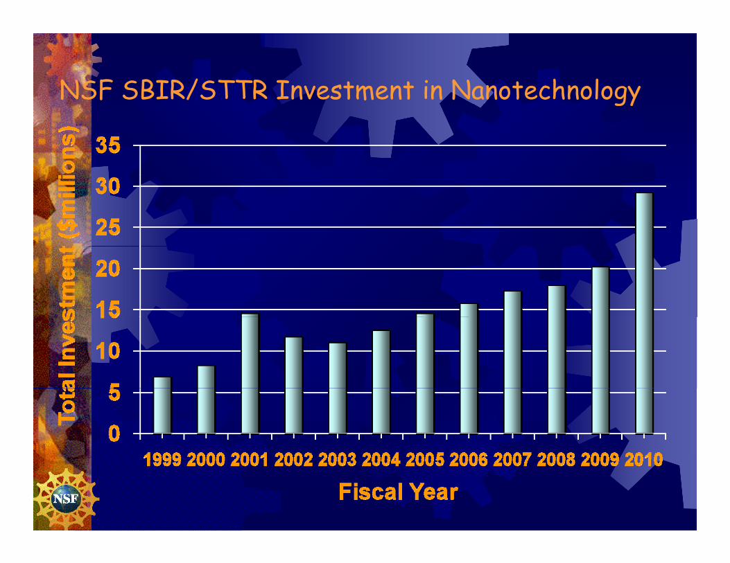
NSF SBIR/STTR Investment in Nanotechnologygy

NSF SBIR/STTR Investment in Nanotechnology (FY 2010)Nanotechnology (FY 2010)
EHS 2%NanomanufacturingNanomanufacturing
12%
Instrumentation Instrumentation for Nano
10%Nanomaterials
58%
Nano Device and Systems
18%18%
Examples of Nanotechnology A li tiApplicationsSelected examples of nanotechnologySelected examples of nanotechnology
applications funded by SBIR/STTR program at NSF through FY 2008program at NSF through FY 2008

Nano - composites

0848645 – Advanced Polymer Matrix Composites Based on Nanofiber Fused Microfiber (Nf2-M) ArchitecturePerformance Polymer Solutions, IncImpact NoveltyImpact
Aerospace applications call for materials that provide weight reduction while maintaining performance
Nf2-M reinforcements provide significant
Novelty Carbon nanotubes grown
from the surface of continuous fibers
Low cost easily scaleableNf M reinforcements provide significant performance increases in composite parts
25X increase in composite electrical conductivity
5X increase in composite thermal conductivity
Low cost, easily scaleable, continuous process
No modification to existing composite manufacturing infrastructure5X increase in composite thermal conductivity
Structural, thermal, electrical aerospace applications (de-icing, lightning strike, numerous structural applications)
infrastructure Successfully demonstrated
on carbon, glass, alumina, quartz, silicon carbide fiber
C Mi iLineage P2SI owns IP, U.S.
Patent 7,338,684 Related Work:
Company Mission Utilizing our patented Nf2-M process, our
mission is to introduce a new platform of reinforcement materials for the aerospace
- N68335-10-C-0176- N68335-07-C-0152
industry that demonstrate significant increases in composite mechanical, thermal, and electrical performance.
Team: Dr. Jason Lincoln (PI), P2SI- N00015-09-1-0925
Dr. David Curliss, P2SIMr. Zach McHale, P2SI

Dry Thermal Adhesive Tape Based on Carbon Dry Thermal Adhesive Tape Based on Carbon NanotubesNanotubesAtlas NanotechnologiesAtlas NanotechnologiesPI: Yang Zhao PI: Yang Zhao -- [email protected]@atlasnanotechnologies.com
Atlas Nanotechnologies
gg y @ gy @ g
IMPACTIMPACT• Enables smaller, more
l d hi h
NOVELTYNOVELTYDouble-Sided
Fl ibl CNT Tcomplex and higher power density electrical and mechanical devices
two surfaces together without residue via
Flexible CNT Tape
Strongly adheres
• High thermal conductancewithout messy grease
two surfaces together without residue via nano scale Van der Waals forces
ABOUT ATLASABOUT ATLASABOUT ATLASABOUT ATLASOur mission is to bring to market adhesive tape products based on CNTs that provide
enhanced thermal and electrical
LINEAGELINEAGE• Progression from 1cm2 to 100cm2 CNT (wafer level) tapes through the use of a custom built production scale furnace
LINEAGELINEAGE• • Progression from 1cm2 to 100cm2 CNT (wafer level) tapes through the use of a custom built production scale furnace conductivity in a reusable adhesive tape
Scientific Team:
• Dr. Ali Kashani, Chief Operations and Scientific Officer • Yang Zhao, Chief Technology Officer
• Jay Longson VP of Research
built production scale furnace• Scalable production of Single and Double sided flexible CNT tapes• Greater CNT array adhesion than the gecko
built production scale furnace• Scalable production of Single and Double sided flexible CNT tapes• Greater CNT array adhesion than the gecko
• Jay Longson, VP of Research • Plus additional Nanotechnology experts
Commercialization Team: • Rob Steir, Todd Smith, Stew Sando
(combined 70 years of business experience)
foot• 10x lower thermal interface resistance than off-the-shelf thermal greases
foot• 10x lower thermal interface resistance than off-the-shelf thermal greases

STTR Phase II Metal Oxide Nanofibers for Filter and Catalyst Support StructuresGrant Number 0822914Company MemPro Ceramics CorporationPI Dr. Gary Carlson
PO Box 250, Akron, OH 44309Ph.: 303.386.5471 Email: [email protected] www.mempro.com www.noxfox.com
Impact Novelty
Increased catalyst efficiency
Market Factors Technology Synopsis
Catalyst support media
Expanded thermal stability
Allows OEMs and catalyst suppliers to expand current product offerings and market sectors
Societal Factors
Various ceramic materials
Produced by electrospinning followed by calcination
Material Advantages Al2O3/Pd Nanofiber Increase chemical production efficiencies
Pollution reduction and control
Enhanced particulate removal from industrial and motor vehicle emissions
ate a d a tages 2 3
Favorable catalyst particle size and dispersion
Enhanced thermal stability
Lightweight
Lineage Company MissionTechnology Origins
Co-developed by MemPro and the University of Akron 1993 I i i l h l d l
Innovation Vision
Develop an array of cost effective, environmentally sound materials into various products or sold as nanofiber materials
O / f 1993 Initial technology development 2001 Investigations into ceramic nanofiber production 2005 Patent issued on the use of catalysts within nanofibers
to OEMs and/or catalyst product manufacturers
The Innovation Team 2005 MemPro acquires license from University of Akron 2007 Production of ceramic nanofibers with noble metals 2009 Patent pending – CCN for engine exhaust treatment
Collaboration between MemPro Ceramics Corporation and the University of Akron (Akron, OH)
Dr. Gary Carlson, PEPrincipal Investigator
Dr. George ChaseThe University of AkronDepartment of Chemical EngineeringCo‐Principal Investigator

Nanocomposite Foil for Bonding Reactive Nanotechnologies IncReactive Nanotechnologies, Inc
NanoBond® Joining of El t i C tElectronic Components
Enables direct solder attach between silicon and
Copper Heat Spreader
attach between silicon and thermal management components without exposing them to reflowIndium Solder Layer
Indium Solder Layer
NanoFoil®exposing them to reflow temperatures
High thermal conductivity:
Indium Solder Layer
Silicon Dieg y
4-8X improvement over current commercial solutionsJoining Configuration solutions
Lower residual stress Bond dissimilar materials
g g

Nano-instrumentation

NSF Grant # 0750512 - Nanoscale Chemical ImagingAnasys Instruments - Kevin KjollerAnasys Instruments Kevin Kjoller
Impact (Market/Societal) Adds chemical measurements to the
SPM capabilities
Novelty Breaks the diffraction limit for IR microspectroscopy
providing spatial resolution up to 100 nmP id t h h i l h i l d
Provides high resolution spectroscopic imaging to the FTIR and IR microscope users
Primary markets
Provides topography, chemical, mechanical and thermal measurements in an integrated SPM system
IR spectra directly comparable to FTIR absorption spectra allowing usage of the vast FTIR libraries
Polymers Life Sciences
Technology
C=OC-O
Amide IA id II
Initially invented by A. Dazzi
Developed and P t t d b
Company / Mission
Amide II
Patented by Anasys Instruments
Quantitative nanoscale property measurements based on probe technologies
Proprietary IP and technology breakthroughsbreakthroughs
Team: Kevin Kjoller: VP / Product
Development Craig Prater: CTO

Phase II STTR: Diamond Nanoprobes for Atomic Force Microscopy
Ad d Di d T h l i IAdvanced Diamond Technologies, Inc.J.A. Carlisle (PI)
Impact NoveltyImpact Enables new industrial applications for AFM (advanced
metrology, nanomanufactoring
Enables new scientific applications, including advanced nanotribology and nanomechanics experiments
Novelty First diamond MEMS devices made with high yields that
meet specifications (frequencies, force constants)
First successful production of monolithic diamond AFM probes, NaDiaProbes™, suitable for use in a broadnanotribology and nanomechanics experiments
Enables new applications that take advantage of molded diamond structures
Provides outstanding training for personnel micro/nanofabrication, advanced materials, and
t h l
probes, NaDiaProbes , suitable for use in a broad variety of AFM instruments.
First direct comparisons of dimensional stability between probes made of different materials, using known theories of contact mechanics.
nanotechnology
Company Mission TEAM: ADT, Uni. of Pennsylvania (R. Carpick), Uni. Of
3 5 nm
0.2 nm
3 5 nm
0.2 nmLineage
Ult t lli di d Wisconsin (K. Turner), several grad. students and posdocs
Develop UNCD-enabled Microdevices leveraging process improvements developed with NSF’s SBIR support
Overcome technical barriers as needed to bring a NaDiaProbe product line to market for general purpose
3-5 nm3-5 nm Ultrananocrystalline diamond (UNCD® ) originally developed at Argonne National Laboratory.
ADT founded in 2003 to commercialize the technology (first NaDiaProbe product line to market for general purpose
contact and dynamic mode imaging.
Refine the understanding of tip/substrate nanoscale processes and interactions and correlate with probe fabrication processes and performance.Visit ADT on the web at www.thindiamond.com
gy (ANL spinout).
ADT today: 17 employees, selling three product families (wafers, seals, probes).

Environmental nanotechnology

Water Purification Technology for the Removal of Chemical & Biological ContaminantsChemical & Biological ContaminantsCrystal Clear Technologies, Inc.Lisa M. Farmen
NOVELTYIMPACTNMX™ nano-coated filter media
can be recharged, with a “doublesticky tape” ligand and accumulatenumerous layers of metal before
IMPACT• Industrial: Removes metal contaminants
without generating a waste stream.y
the media exhausts.• Societal: Technology can purify enough
water for one person for a year for $1.00
LINEAGE: Funding from Siemens for field test Validation samples at Dow Water MOU ith CDI f OEM f t i
COMPANY MISSION MOU with CDI for OEM manufacturing Sandia Nat’l. Labs – filter testing CRADA – NUS, NRL, UO Licensing with Ga Tech/NUS ONAMI Gap Grant $225K
To commercialize low cost waterpurification products at a costaffordable to the majority of theworld’s population.p p
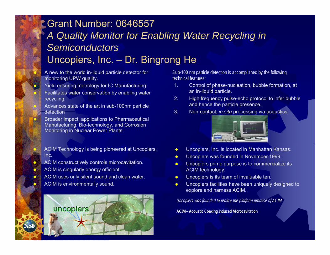
Grant Number: 0646557A Quality Monitor for Enabling Water Recycling in SemiconductorsSemiconductorsUncopiers, Inc. – Dr. Bingrong He
A new to the world in-liquid particle detector for monitoring UPW quality
Sub-100 nm particle detection is accomplished by the following technical features:monitoring UPW quality.
Yield ensuring metrology for IC Manufacturing. Facilitates water conservation by enabling water
recycling. Advances state of the art in sub-100nm particle
detection
1. Control of phase-nucleation, bubble formation, at an in-liquid particle.
2. High frequency pulse-echo protocol to infer bubble and hence the particle presence.
3 Non contact in situ processing via acoustics
technical features:
detection Broader impact: applications to Pharmaceutical
Manufacturing, Bio-technology, and Corrosion Monitoring in Nuclear Power Plants.
3. Non-contact, in situ processing via acoustics.
ACIM Technology is being pioneered at Uncopiers, Inc.
ACIM constructively controls microcavitation. ACIM is singularly energy efficient. ACIM uses only silent sound and clean water
Uncopiers, Inc. is located in Manhattan Kansas. Uncopiers was founded in November 1999. Uncopiers prime purpose is to commercialize its
ACIM technology. U i i it t f i l bl t ACIM uses only silent sound and clean water.
ACIM is environmentally sound. Uncopiers is its team of invaluable ten. Uncopiers facilities have been uniquely designed to
explore and harness ACIM.
Uncopiers was founded to realize the platform promise of ACIM
ACIM – Acoustic Coaxing Induced Microcavitation

Nano coatingsNano - coatings
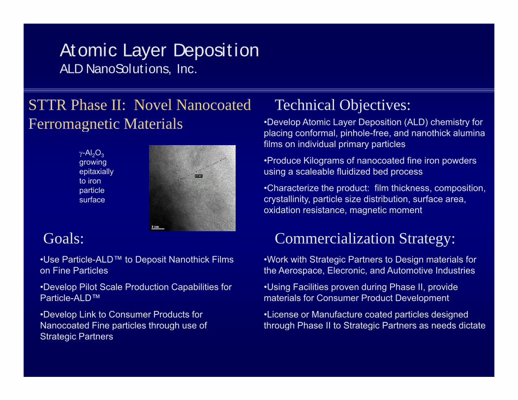
Atomic Layer DepositionALD NanoSolutions, Inc.,
STTR Phase II: Novel Nanocoated Ferromagnetic Materials
Technical Objectives:•Develop Atomic Layer Deposition (ALD) chemistry forFerromagnetic Materials Develop Atomic Layer Deposition (ALD) chemistry for placing conformal, pinhole-free, and nanothick alumina films on individual primary particles
•Produce Kilograms of nanocoated fine iron powders using a scaleable fluidized bed process
-Al2O3growingepitaxially g p
•Characterize the product: film thickness, composition, crystallinity, particle size distribution, surface area, oxidation resistance, magnetic moment
p yto ironparticlesurface
Goals: Commercialization Strategy:•Use Particle-ALD™ to Deposit Nanothick Films on Fine Particles
•Work with Strategic Partners to Design materials for the Aerospace, Elecronic, and Automotive Industries
•Develop Pilot Scale Production Capabilities for Particle-ALD™
•Develop Link to Consumer Products for Nanocoated Fine particles through use of
•Using Facilities proven during Phase II, provide materials for Consumer Product Development
•License or Manufacture coated particles designed through Phase II to Strategic Partners as needs dictateNanocoated Fine particles through use of
Strategic Partnersthrough Phase II to Strategic Partners as needs dictate

Ultrananocrystalline Diamond as Wear Resistant and Protective Coating for Mechanical Shaft Seal ApplicationsAdvanced Diamond Technologies, Inc.
Impact John Crane offers largest product line
g ,
Noveltyf f % John Crane offers largest product line
with UNCD®
Advanced Diamond Technologies, Inc. (ADT) selling UNCD seals to direct users (www diamondseals com)
Reduction in seal face friction by 75% Multiples of decrease in wear from SiC in
accelerated wear testing with hot-water (250F, 150 psig).
(www.diamondseals.com) Reduced energy
consumption, wear
Smooth diamond suitable for use with conventional mating ring
Company Mission TEAM: ADT (prime) ANL
Lineage UNCD resulted from 10+ years of R&D at TEAM: ADT (prime), ANL,
John Crane NA Product-oriented company focused on thin,
smooth diamondW l h d bl ™
DOE’s Argonne National Laboratory (ANL) Advanced Diamond Technologies, Inc.
spun out of ANL in 2003, and is exclusive commercial source of UNCD.
We solve hard problems™co e c a sou ce o U C Other products in market or development
include UNCD wafers, AFM probes, supported by NSF SBIR programs
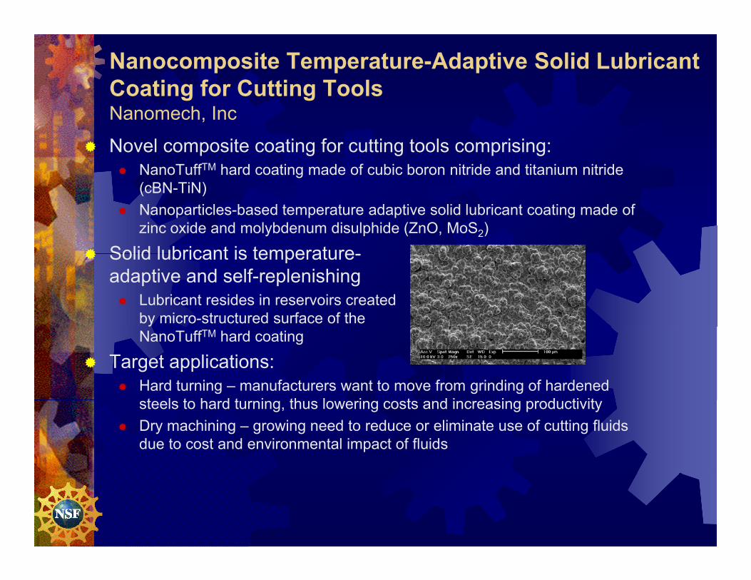
Nanocomposite Temperature-Adaptive Solid Lubricant Coating for Cutting ToolsN h INanomech, Inc
Novel composite coating for cutting tools comprising: NanoTuffTM hard coating made of cubic boron nitride and titanium nitride
(cBN-TiN) Nanoparticles-based temperature adaptive solid lubricant coating made of
zinc oxide and molybdenum disulphide (ZnO, MoS2)
Solid lubricant is temperature Solid lubricant is temperature-adaptive and self-replenishing Lubricant resides in reservoirs created
by micro-structured surface of theNanoTuffTM hard coating
Target applications: Hard turning – manufacturers want to move from grinding of hardened
t l t h d t i th l i t d i i d ti itsteels to hard turning, thus lowering costs and increasing productivity Dry machining – growing need to reduce or eliminate use of cutting fluids
due to cost and environmental impact of fluids

SBIR Phase II Title: SBIR Phase II Title: “Fe“Fe--nanoparticlenanoparticle Coating of Anisotropic Magnet Powder for Coating of Anisotropic Magnet Powder for NanocompositeNanocomposite Permanent Permanent Magnets ith Enhanced (BH)Magnets ith Enhanced (BH) ””
NSF Grant Number: IIP-0848996
Magnets with Enhanced (BH)Magnets with Enhanced (BH)maxmax””Company Name: Electron Energy Corporation (Landisville, PA)PI Name: Jinfang Liu
Novelty (Technical)Impact (Market/Societal) y ( )p ( / )
If successfully implemented into practice, the proposed technology could lead to the development of anew class of high performance nanocomposite magnets with much higher maximum energy product,(BH)max or magnetic strength.
This technology could have a significant impact in many devices in which the actuation or sensing is
If the proposed technology can approach the theoretical performance potential of double the current state of the art rare earth magnets, it would have a dramatic impact on permanent magnet markets and applications.
Fe(‐Co)
The objective of this project is the synthesis of composite magnet powders coated with Fe or Fe-based nanoparticles forthe development of permanent magnets with superior magnetic properties. A sketch of the morphology of the(nano)composite powders and consolidated nanocomposite magnets is shown below.
Iron Nanoparticles
based on a magnetic field produced by permanent magnets. The applications include consumerelectronics, renewable energy, electric vehicles, medical and military applications, etc.
(a) (b) (c)
Substrate particle
Fe( Co)
nanolayer
Partial nanoparticle coating
(a)
(b)
(c)
Substrate Particle
NanoparticlesFe(Co)
Morphology of the composite powders consolidated into a permanent magnetComplete & uniform coating
Lineage (Origins of the Technology) Company Mission (Include the Team)CompanyCompany MissionMission:: to be specialists in rare earth magnets and magnet systems, providing innovativesolutions for precise technical challenges.Project partner:Project partner: University of Delaware, Department of Physics and Astronomy, Prof. George Hadjipanayis’s Group.
EEC Key PersonnelEEC Key Personnel
1990s: Theoretical prediction that two phase nanocomposite magnets consisting of • hard magnetic phase • soft magnetic phase
Nanocompositesmper
ature
(o C)
Dr. Jinfang Liu, V.P. of Technology and Engineering, plays a leadership role in magnet material’s development as well as magnet applications development for the company.
Dr. Melania Marinescu, Manager of Process Technology, focuses on theimprovement of magnetic performance of the current permanent magnets throughprocess and chemistry optimizations and the development of new (nano)compositemagnets
Current SBIR data: Back scattered electron SEM micrographs of
EEC Key PersonnelEEC Key Personnelmay exhibit a maximum energy product (BH)max twice the value of the current magnets.
a oco pos tes
(BH)max (MGOe)
Tem
This research was sponsored by the NASA Glen Research Center under the Grant NNC06CA04C.
magnets.
Peter C. Dent, V.P. of New Business Development, is responsible for leadingthe product introduction to the market and product licensing programs.
ISO 9001:2000
composite magnets with different morphologies, consisting of ahard magnetic phase (rare earth –based intermetalliccompound) surrounded by a soft magnetic phase (Fenanoparticles).

Nano biotechnologNano - biotechnology

Targeted Drug Delivery Nanospectra Biosciences, IncAuroShells Injected into Blood Will Exit Through Holes
d L d i T T V l Rand Lodge in Tumor, Target Vasculature Receptors
TumorC
Y
Blood
Cells
Y YY BloodSupply
Y
YY
26
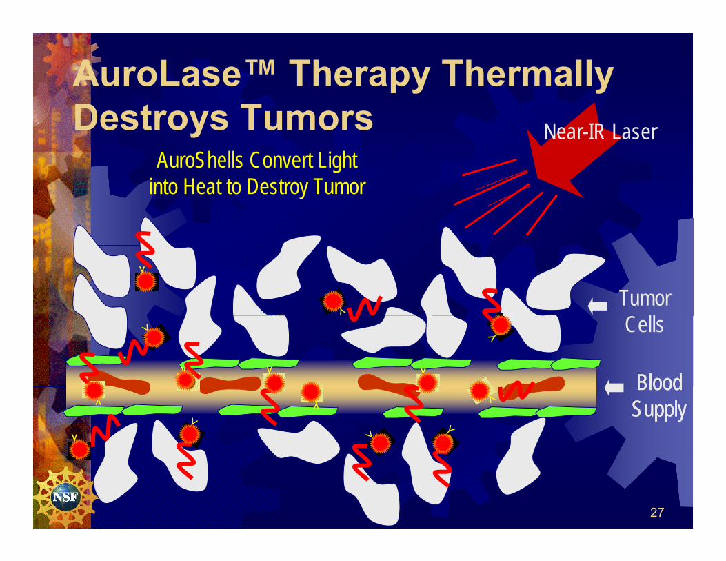
AuroLase™ Therapy Thermally D TDestroys Tumors Near-IR Laser
AuroShells Convert Lightinto Heat to Destroy Tumor
TumorC
Y
BloodBlood
Cells
Y YY BloodSupplyBloodSupply
Y
YY
27

Synthetic Bone Material NanOss™Synthetic Bone Material -NanOss™Angstrom Medica
Structural Medical Devices Osteoconductive Remodels into Bone Over Time Remodels into Bone Over Time
Injectable Cement Endothermic, Rapid-setting Structural, Weight-bearing
Bioactive Coatings Micron Thicknesses Can Act as a Carrier
Proprietary and Confidential
Can Act as a Carrier

#0620563Nanocomposite Coating on Coronary StentsNanocopoeia IncNanocopoeia, Inc.Robert Hoerr, MD, PhD
Drug and medical devices Drug/polymer combinations a growing trend Coronary stents first
blockbuster example Broad market opportunities
combinations Non-line-of-sight
coatings on complex structures e
30
Broad market opportunities Modify the body’s response to
implanted devices
structures Able to engineer/control
drug release profilesDays
0 5 10 15 20 25 30
Dex
amet
haso
ne %
Dos
0
5
10
15
20
25
TPE4 Open MatrixTPE4 Hybrid SF Inner, OM OuterTPE4 Smooth Film
ElectroNanospray™ technology U Minnesota
Bring novel drug delivery applications to market that solve clinical challenges
David Pui, Daren Chen inventors
Nanocopoeia improvements
Drug coatings to improve therapeutic performance of medical device implants, including stents
p World-wide exclusive
license

STTR Grant Number : 0620572 “Antibacterially-Active Nanoparticles”Nanopharma Technologies, Inc.D Ed d T S JDrs. Edward Turos, Seyoung Jang
Impact Novelty (Technical) Impact (Market/Societal)
Novelty (Technical)Nanobiotics Pen G-nanoparticlesAntibiotics
Lineage (Origins of the Company Mission
Platform Technologies for Biodefense and Nanoscience
* Infectious Diseases (MRSA) Treatment* Target delivery and rejuvenation
g ( gTechnology)
Company Mission
Development ofNanoparticle Drug Delivery Platformfor delivery of water-insoluble drugsto greatly enhance the efficiency and enzyme stability of antibiotic agentsproviding a potential means to clinically
O
N S
N
O
O
providing a potential means to clinically overcome resistance that the infectious agent has acquired to an antibiotic such as penicillin.
N S
HOOC
MRSA MIC = 2 µg/mL Scanning Electron Microscope Image

Nano electronicsNano - electronics

Thin Film Transistors: Silicon NanowiresNanosys, Inc
High Performance, large area nano-structured macro-electronics substrate technology
TFT Backplane Drivers – Integrated Edge Electronics
Beam-Steering Antennas
Eli i t hi h t t t i d f i d t• Eliminates high-temperature steps required for semiconductordeposition
• Dramatically reduces manufacturing cost, time and complexity
• Deposition on virtually any substrate material possible
RFID Tags
Deposition on virtually any substrate material possible
A variety of application areas:
• Portable & large-area flat panel displays
• Low-cost RFID and smart cards
•Electronically steerable phased-array RF antennas

IIP-0848490Ultralow κ Interlayer Dielectrics for 22nm Node and BeyondDendritech, Inc. PI: Petar Dvornic ,
ImpactTarget: Ultralow K <2 interlayer dielectrics
NoveltyPAMAMOS dendrimers form covalently crosslinked g y
to enable “next gen” chips (ITRS Roadmap)
Minimizing “crosstalk” between chip layers permits faster, smaller semiconductors f d i ti d
yhoneycomb networks by spin-on and cure
Closed-cell nanoporosity (2-4 nm) introduced upon thermal degradation to form insulator
for device computing power and miniaturization
Ultralow K ILD forecast >$150MM in 2012
Lineage- Dendrimers, a new class ofpolymer architecture wereinvented in late 1970’s 1980’s
Company Mission-Commercial supply of PAMAMdendrimers for enhanced value in
invented in late 1970’s-1980’s- Commercial production ofPAMAM (polyamidoamine)dendrimers begins at Dendritech(1990’s)
customer products-Custom-built plant for reliable supplyof PAMAM dendrimers since 1994-6 patents on PAMAMOS dendrimers( )
- Patented invention of the firstsilicon-containing dendrimers(PAMAMOS) in 1990’s-2000’s
Team: Dr. Petar Dvornic, PI Dr. Steven Kaganove, R&DEmery Scheibert, ManufacturingMark Kaiser, Market Development

NSF SBIR Phase II Grant IIP- 0822652
High-Efficiency Nanocomposite Photovoltaics and Solar CellsANTEOS, Inc.,PI - Dr. Valery Rupasov
Impact (Market/Societal) Novelty (Technical)
• Projected revenue of the market of solar cells - $23.1B • Thin-film amorphous silicon (TFAS) solar cells capture
20% of the market. • Increasing power efficiency from 6-7.5% up to 10%
would have dramatic impact on the market
Power efficiency of low-cost and mature TFAS solar cells is increased by
• Using the effect of Multiple Exciton Generation (MEG) in would have dramatic impact on the market Exciton Generation (MEG) in quantum-confined semiconductor nanocrystalsembedded into amorphous Sip-n junction and
Lineage (Origins of the Technology) Company Mission (Team)
• Fast separation of the electron-hole pairs in built-in electric field of the p-n junction
Lineage (Origins of the Technology) Company Mission (Team)
• Demonstration of Multiple Exciton Generation (MEG)in semiconductor nanocrystals (LANL, NREL)
• Patent pending invention of company president,
Mission: Development of the emerging nano-technology and manufacturing of the nanocrystal solar cells
Team: Dr. Sergei Krivoshlykov (project management, technology development & commercialization) Dr. Valery Rupasov p g p y p
Dr. S. Krivoshlykov, who proposed to incorporate thesemiconductor nanocrystals into amorphous silicon p-n junction (Patent Application: 11/439,626)
p ) y p(theoretical estimates)
Seeking: Equity Investment & Partnership for product manufacturing and marketing.
Photovoltaics : Nanoparticle co-sensitizers for increased efficiency.yKonarka, Inc
From Light to Power Polymer photovoltaic products in a variety of
form factors for commercial, industrial,
military and consumer applications
• Uses photoactive dyes & conducting polymers
• High-speed manufacturing processes
• Low temperature environment
• Uses low cost materials
• Highly scaleable
Total thickness 0.01 inch• Mass customization from a single source
• World solar PV market: CAGR > 35%
• Highly scaleable
Schematic of Dye Sensitized Titania Cell
Plastic
FoilActive LayerTransparent Conductor + CatalystPlastic
• 20+ patents pending

Spintronics Non-volatile MemoryGrandis, Inc
5
6
7
8
kOhm
) High resistance
{1} Spin Transfer Torque RAM (STT-RAM) Fast: less than 10ns read/write Non-volatile memory: >10 year lifetime
1
2
3
4
5
Resistanc
e (k
{0}
Non-volatile memory: >10 year lifetime Scalable: beyond 65nm Low Power Multiple bits per cell capable
0
1
Current
Low resistance
(A)
Multiple bits per cell capable Compatible with semiconductor processes
SBIR PHASE II GrantAllo s Grandis to contin e materials research to enable an ad anced Allows Grandis to continue materials research to enable an advanced demo chip to accelerate commercialization.
Storage layer (free)
“1”Bit Line
“0”Bit Line
BarrierReference layer (pinned)(Spin filter)
Storage layer (free)
Current
Copyright © 2007 Grandis, Inc
Source Line
SelectionTransistorSource LineSource Line

Lithium Ion BatteriesT
JT/J
Technologies, Inc.
Technology:High Rate, High Capacity Anodes for Rechargeable Li Batteries Based on
Outside Investment
NASA Contract: $2,200,000Metal Oxide Nano Composites
NASA Contract: $2,200,000Acquired by A123 CompanyMetal oxide
Goals:• Reduce irreversible capacity to <15%
Commercialization Strategy:• System payoff:
1 micronConductive phase
• >300 mAh/g reversible capacity
>10C at 80% rated capacity and 80% DOD
y p y30-50% reduction in large format lithium-ion battery size
•Develop a cost-competitive battery suitable
Achieve projected material costs of <$10/kg
p p yfor HEV, UPS, military and aerospace applications
•Strategic Partnerships for joint development g p j pof new materials:materials production and battery manufacturing

. Lithium Reservoir Nanocarbons for Lithium Ion Batteries
Applied Sciences, Inc
IMPACT NOVELTY
Enables Long-Range HEVs and EVs Supports Alternative Energy Use
• High Capacity Anodes for Li-Ion Battery
S f P f i B ttpp gy
Reduces Emissions Reduces Dependence Upon Foreign Oil
• Safe Performing Battery
Creates Domestic Manufacturing Jobs LINEAGE
• TechnologyCOMPANY MISSION
gy• Carbon Nanofiber – GM, ASI, PPI• Anode – ASI, PPI, GM, Others
• Funding Source
• High Performance Li-Ion Battery → Chevy Volt• Insertion in 2011 at 30 k lb/yr
$8 M i t t f 400 k lb/ d d ig• NSF → GM → Ohio Fund → A123
• $3 M Secured
• $8 M investment for 400 k lb/yr demand in 2013• Revenues of $26 M by 2013• ROI > 45% in 2013

Nano man fact ringNano - manufacturing

IIP-0822808Automotive NanocompositesClaytec, Inc.C ay ec, cPI: Joel Dulebohn, Ph.D.
Impact NoveltyImpact• Stronger, stiffer, lighter and cheaper plastics • Lighter automobiles with improved fuel
efficiency• Reduction in CO2 emissions
• Porous frameworks allow for particle networking•Low cost, non-toxic synthetic silicate nanoparticles• Dispersible without the need for surface modifiers
Reduction in CO2 emissions • Enhanced barrier properties, improved durability• Recyclable plastics for a longer life cycle Represents a highly competitive new niche in the
l b l l dd d$66 B global polymer additives industryLineage
Michigan State University• NSF – funded basic research on metal
oxides with intracrystal porosity and high
Company MissionThomas J. Pinnavaia – PresidentJoel Dulebohn, Ph.D. – Operations ManagerSeongSu Kim Ph D Senior Scientistoxides with intracrystal porosity and high
surface areas (1992-2004)• International patent applications (2004-
2008)Claytec, Inc.
SeongSu Kim, Ph.D. – Senior Scientist
Claytec, Inc. solves challenging chemical and material problems through innovative porous metal oxide chemistry. Our mission includes the development of porous nanoparticles for advanced applications in
• NSF-SBIR Phase I (January 2007)• Licensing of patents (2004 – 2008)• NSF-Phase II (2008-2010)
p p ppautomotive, green energy (wind turbines), electrical cables, and catalytic bio-fuel production.

Supercritical Fluid Processing of Polymer/Clay Nanocomposites
Novelty
nanoScience Engineering CorporationSteve Horsch
Impact m2 )
105
106
105
106
G' PSG" PSG' 9wt% Cloisite 93A / PSG" 9wt% Cloisite 93A / PSy
Green, economical process Highly dispersed nanofillers Improved mechanical, thermal
p Create jobs Create wealth for investors Increase shelf-life of perishables
aT (rad/s) (Tref = 140oC)
10-3 10-2 10-1 100 101 102 103
G' G
" (d
yne/
cm
101
102
103
104
101
102
103
104
T (oC)120 130 140 150 160 170 180
a T
10-2
10-1
100
101
9wt% 93APS
Improved mechanical, thermal properties
Improved barrier properties
Increase shelf life of perishables Introduce high performance
nanocomposites in products
Lineage Joint Development Agreements
Company Mission Value: Highly dispersed nanofillers
at a competitive price
Raised $500,000 venture capital/investors
at a competitive price Team: Experienced entrepreneurs
and Research Scientists Exit Strategy: IPO, Strategic capital/investors
Collaboration with WSU/Clemson
gy gPartnership, or Sale

SBIR Phase IIB: Commercial Combustion Synthesis of Homogeneous Lots of Carbon
Nanotubes (IIP-0522093)Henning Richter, [email protected]
L l f t f i l ll dImpact Novelty
l b h f Large-scale manufacture of single-walledcarbon nanotubes (SWCNT)
- Energy generation and storageElectronics and sensors
Selective combustion synthesis of (SWCNT) or fullerenes
Exothermic, scalable, reproducible h l- Electronics and sensors
- Improvement of polymer properties- Filtration and separation
Length control Hydrogen formation
Li C Mi iLineage Founded in 2001 to commercialize MIT
technology
Company Mission Leading manufacturer of fullerenic
materials and derivatives, licensor- license for fullerene synthesis in Japan
Development contracts in place
5+ patents, >10 pending and in-licensed
Experienced technical and business team Capture downstream value by internal
and collaborative application workp , p g
$ 7 MM invested between ’01 and ‘09
$2.9 MM NIST ATP award
Major development effort in SWCNT dispersions and their use for transparent conducting films

Silicon Nanoparticles ManufaturingInnovalight, Inc
Continuous Flow Reactor & Size-Selection Scheme for Use
Technical Objectives:• High quantum yieldsSize Selection Scheme for Use
in High Throughput Manufacture of Si Nanoparticles
High quantum yields• Tunable emission• Defect-free particles
Goals:• Si nanomanufacturing system• Process parameters
Commercialization Strategy:• IP portfolio• Cell phones exit lighting• Process parameters
• 5 grams/hour• Cell phones, exit lighting
(short term)• Solid-State Lighting
f

Gentle Atomic Level Chemical Mechanical Smoothening (CMS) of Gallium Nitride Substrates
Sinmat inc
Impact Increasing demand for
WBG devices for RF,
Sinmat, inc
Novelty Novel polishing process
(chemistry particles etc ) for
a RMS 2 Å
WBG devices for RF, power & opto-electronic applications
GaN components sales >$7.2 Billion by 2009
(chemistry, particles, etc.) for bulk GaN & GaN films on various substrates
Atomic level polishing High removal rate b RMS 7 Åy
Great potential for energy saving devices
Creation of new hi-techR&D and manufacturing j b
High removal rate Uniform, low defect polish over
large area: high yield/low cost Scalable > 2” substrates Good reproducibility
jobs
Sinmat Inc.’s Mission & Goals Establish a leadership position in providing
p y
Lineage Idea conceived and developed at Sinmat Inc. Patent applications in preparation value-driven semiconductor solutions to industry
on planarization technologies Establish strategic industrial partnerships for
R&D, marketing, sales, & services Build up Intellectual Property portfolio ( 5
Patent applications in preparation Selective results have been published Collaborations with University of Florida (UF)
for film deposition, device fabrication, testingd d t l i Build up Intellectual Property portfolio ( 5
licensed patents & several pending applications) Teams: Sinmat scientists (9 PhDs); UF (Profs.
Pearton & Abernathy); Advisors & Consultants
and data analysis Several companies interested in Sinmat’s
process, and supplying substrates for evaluation of GaN polishing process

SummarySummary In FY 2010 the NSF SBIR/STTR
d 140 l t dprogram made over 140 nano-related grants and over 40 supplemental grants to small companies totaling $ 29 MMto small companies totaling $ 29 MM.
Across the whole Federal government SBIR/STTR programs accounted for close to $100 MM in nano-related grants (FY 08).

NSF SBIR/STTR Home Page
www.nsf.gov/eng/iip/sbirwww.nsf.gov/eng/iip/sbirwww.nsf.gov/eng/iip/sbirwww.nsf.gov/eng/iip/sbir
Thank YouThank YouJ R ddJ R ddJames RuddJames Ruddtjrudd@nsf govtjrudd@nsf [email protected]@nsf.gov