national infotech - advpowerec.pdf · negative group of thyristors. inbuilt connection of inductor...
TRANSCRIPT

Power electronics is the engineering
study of converting electrical power
from one form to another. World-wide,
at an average rate of 12 billion
kilowatts of electrical energy is
generated in every hour of every day of
every year. The power generated is
being reprocessed or recycled through
some form of power electronic
systems. It is expected that this power
processing will increase up to 80% in
near future. Increased use of Power
electronics demanded new power
converters which do not pollute the
grid. Accordingly many new power
converters are developed.
The use of power electronics in power
system control and power quality
improvements are also increased
extensively.
NITech offers a wide range of advance
power electronics converter kits for
studying new power converters and for
studying application of power
electronics in power system. Kits like
multi-pulse converter, PWM rectifier,
PFC using boost converter, multi-level
inverters are designed. Kits for static
var control (SVC) and harmonic
elimination are also designed.
NATIONAL INFOTECH
A way to Power Electronics and Embedded Systems Solutions...
ADVANCED POWER ELECTRONICS TRAINER
: Developed By :
National Infotech Room No. 202, 2rdFloor, A-19/20,
Road No. 9, Udhyognagar, Udhna,
Surat-394 210, India (South Gujarat).
Phone: +91-9427 752 256.
Email:[email protected]
Web:http://www.national-infotech.com
: Authorized Dealer :
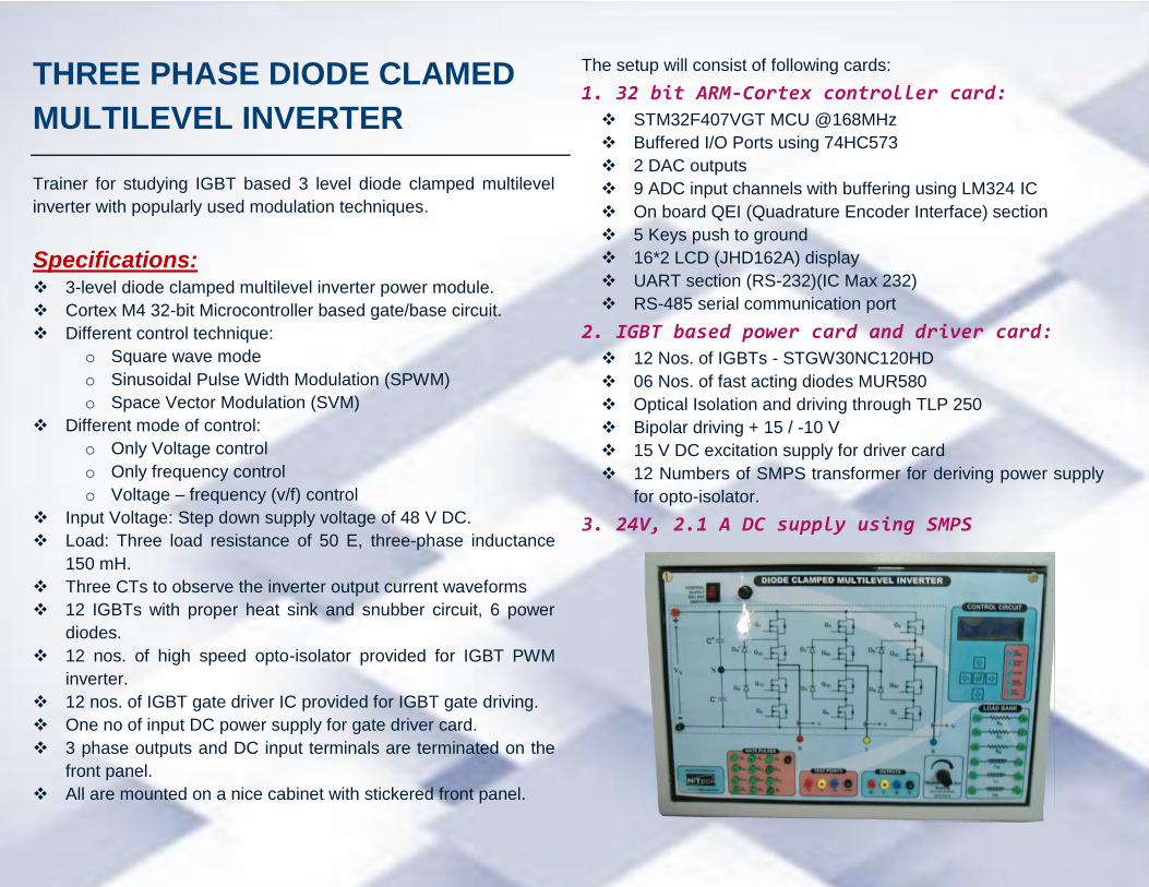
THREE PHASE DIODE CLAMED
MULTILEVEL INVERTER
Trainer for studying IGBT based 3 level diode clamped multilevel
inverter with popularly used modulation techniques.
Specifications: 3-level diode clamped multilevel inverter power module.
Cortex M4 32-bit Microcontroller based gate/base circuit.
Different control technique:
o Square wave mode
o Sinusoidal Pulse Width Modulation (SPWM)
o Space Vector Modulation (SVM)
Different mode of control:
o Only Voltage control
o Only frequency control
o Voltage – frequency (v/f) control
Input Voltage: Step down supply voltage of 48 V DC.
Load: Three load resistance of 50 E, three-phase inductance
150 mH.
Three CTs to observe the inverter output current waveforms
12 IGBTs with proper heat sink and snubber circuit, 6 power
diodes.
12 nos. of high speed opto-isolator provided for IGBT PWM
inverter.
12 nos. of IGBT gate driver IC provided for IGBT gate driving.
One no of input DC power supply for gate driver card.
3 phase outputs and DC input terminals are terminated on the
front panel.
All are mounted on a nice cabinet with stickered front panel.
The setup will consist of following cards:
1. 32 bit ARM-Cortex controller card:
STM32F407VGT MCU @168MHz
Buffered I/O Ports using 74HC573
2 DAC outputs
9 ADC input channels with buffering using LM324 IC
On board QEI (Quadrature Encoder Interface) section
5 Keys push to ground
16*2 LCD (JHD162A) display
UART section (RS-232)(IC Max 232)
RS-485 serial communication port
2. IGBT based power card and driver card:
12 Nos. of IGBTs - STGW30NC120HD
06 Nos. of fast acting diodes MUR580
Optical Isolation and driving through TLP 250
Bipolar driving + 15 / -10 V
15 V DC excitation supply for driver card
12 Numbers of SMPS transformer for deriving power supply
for opto-isolator.
3. 24V, 2.1 A DC supply using SMPS
List of Experiments: Study of gate pulse generating circuit for multilevel inverters.
Study of multilevel inverter in square wave mode with R-
load.
Study of multilevel inverter in square wave mode with R-L
load.
Study of voltage control in multilevel inverter controlled with
SPWM inverter.
Study of voltage control in multilevel inverter controlled with
SVM inverter.
Study of v/f control in multilevel inverter controlled with
SPWM inverter.
Study of v/f control in multilevel inverter controlled with SVM
inverter.
Comparative study of SPWM and SVM control in multilevel
inverter
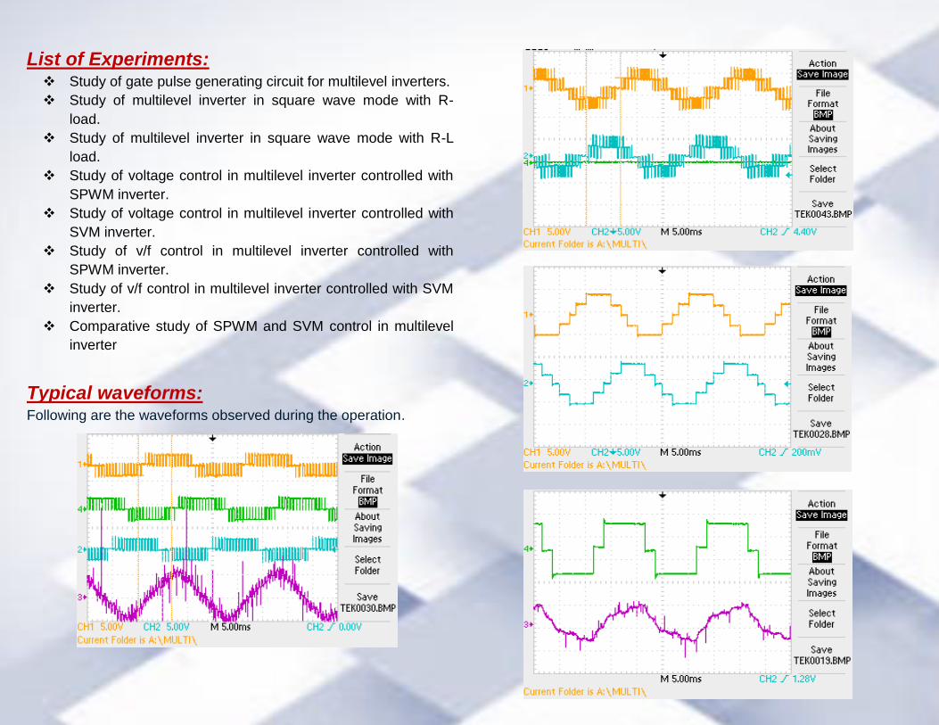
Typical waveforms: Following are the waveforms observed during the operation.
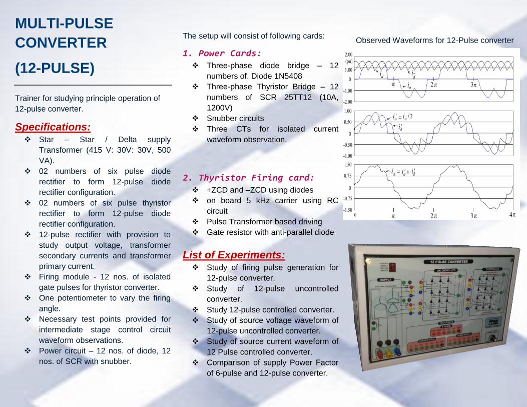
MULTI-PULSE
CONVERTER
(12-PULSE)
Trainer for studying principle operation of
12-pulse converter.
Specifications: Star – Star / Delta supply
Transformer (415 V: 30V: 30V, 500
VA).
02 numbers of six pulse diode
rectifier to form 12-pulse diode
rectifier configuration.
02 numbers of six pulse thyristor
rectifier to form 12-pulse diode
rectifier configuration.
12-pulse rectifier with provision to
study output voltage, transformer
secondary currents and transformer
primary current.
Firing module - 12 nos. of isolated
gate pulses for thyristor converter.
One potentiometer to vary the firing
angle.
Necessary test points provided for
intermediate stage control circuit
waveform observations.
Power circuit – 12 nos. of diode, 12
nos. of SCR with snubber.
The setup will consist of following cards:
1. Power Cards:
Three-phase diode bridge – 12
numbers of. Diode 1N5408
Three-phase Thyristor Bridge – 12
numbers of SCR 25TT12 (10A,
1200V)
Snubber circuits
Three CTs for isolated current
waveform observation.
2. Thyristor Firing card:
+ZCD and –ZCD using diodes
on board 5 kHz carrier using RC
circuit
Pulse Transformer based driving
Gate resistor with anti-parallel diode
List of Experiments: Study of firing pulse generation for
12-pulse converter.
Study of 12-pulse uncontrolled
converter.
Study 12-pulse controlled converter.
Study of source voltage waveform of
12-pulse uncontrolled converter.
Study of source current waveform of
12 Pulse controlled converter.
Comparison of supply Power Factor
of 6-pulse and 12-pulse converter.
Observed Waveforms for 12-Pulse converter
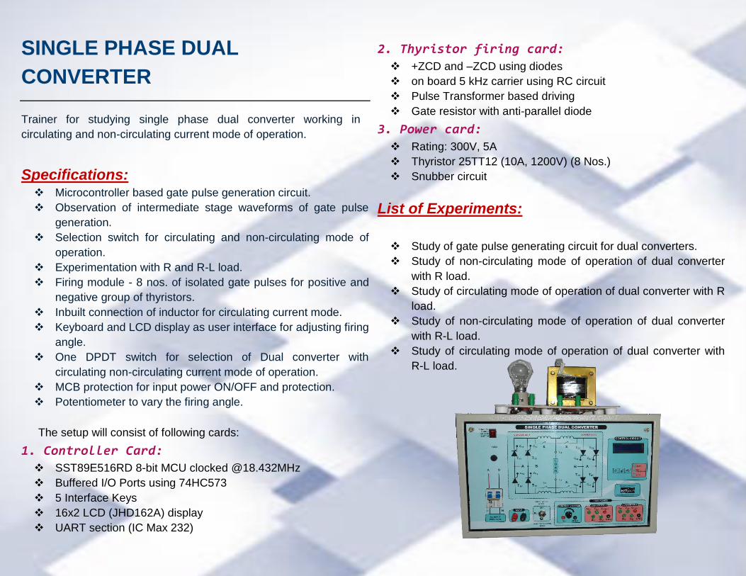
SINGLE PHASE DUAL
CONVERTER
Trainer for studying single phase dual converter working in
circulating and non-circulating current mode of operation.
Specifications: Microcontroller based gate pulse generation circuit.
Observation of intermediate stage waveforms of gate pulse
generation.
Selection switch for circulating and non-circulating mode of
operation.
Experimentation with R and R-L load.
Firing module - 8 nos. of isolated gate pulses for positive and
negative group of thyristors.
Inbuilt connection of inductor for circulating current mode.
Keyboard and LCD display as user interface for adjusting firing
angle.
One DPDT switch for selection of Dual converter with
circulating non-circulating current mode of operation.
MCB protection for input power ON/OFF and protection.
Potentiometer to vary the firing angle.
The setup will consist of following cards:
1. Controller Card:
SST89E516RD 8-bit MCU clocked @18.432MHz
Buffered I/O Ports using 74HC573
5 Interface Keys
16x2 LCD (JHD162A) display
UART section (IC Max 232)
2. Thyristor firing card:
+ZCD and –ZCD using diodes
on board 5 kHz carrier using RC circuit
Pulse Transformer based driving
Gate resistor with anti-parallel diode
3. Power card:
Rating: 300V, 5A
Thyristor 25TT12 (10A, 1200V) (8 Nos.)
Snubber circuit
List of Experiments:
Study of gate pulse generating circuit for dual converters.
Study of non-circulating mode of operation of dual converter
with R load.
Study of circulating mode of operation of dual converter with R
load.
Study of non-circulating mode of operation of dual converter
with R-L load.
Study of circulating mode of operation of dual converter with
R-L load.

SINGLE PHASE THYRISTOR
CONTROLLED REACTOR
Trainer for studying working principle of single phase fixed
capacitor thyristor controlled reactor (FC-TCR).
The kit includes: Microcontroller based gate pulse generation circuit.
Panel for demonstrating TCR and FC-TCR principal
Variable reactive load with fixed inductance and variable
resistance.
Single phase fix capacitor which compensate full load reactive
power.
Reactor with Thyristor controlled branch.
Auto / Manual mode of operation
Measuring of reactive power in different load conditions.
01 CT and 01 PT to observe isolated current and voltage
waveforms.
Observation of intermediate stage waveforms of gate pulse
generation.
Power meter for measuring reactive power and other
parameters.
Specifications: Supply Voltage: 230 V, 50 Hz.
Variable R-L load with switching mechanism. (Three Bulbs
and One Inductor)
One Capacitor Bank
TCR branch with back to back Thyristors and inductor.
1:1000 A CT and 230:6 V PT for isolated observation of
voltage and current waveforms.
Multi-parameter meter (Elmeasure) for measuring power
supply current THD and other parameters.
SST89E516RD MCU @18.432MHz based digital gate pulse
generation circuit.
The setup will consist of following cards:
1. Controller Card:
SST89E516RD 8-bit MCU clocked @18.432MHz
Buffered I/O Ports using 74HC573
5 Interface Keys
16x2 LCD (JHD162A) display
UART section (IC Max 232)
2. Thyristor firing card:
+ZCD and –ZCD using diodes
on board 5 kHz carrier using RC circuit
Pulse Transformer based driving
Gate resistor with anti-parallel diode
3. Power card:
Thyristor 25TT12 (10A, 1200V) (3 Nos.)
Diode 1N5408 (1 Nos.)
Snubber circuit
List of Experiments: Measurement of active and reactive power of the load.
Compensation of reactive power with fixed capacitor.
Study of Thyristor Controlled Reactor (TCR) operation.
Study of reactive power compensation with TCR in open loop.
Compensation with TCR in close loop.
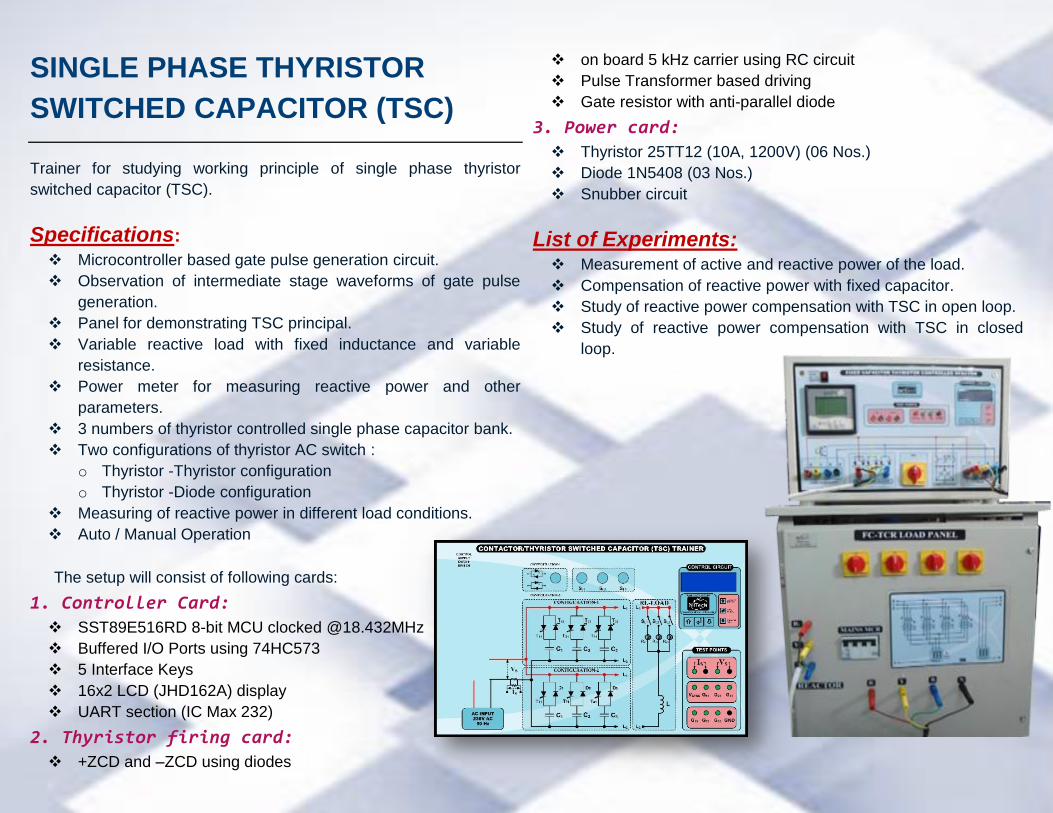
SINGLE PHASE THYRISTOR
SWITCHED CAPACITOR (TSC)
Trainer for studying working principle of single phase thyristor
switched capacitor (TSC).
Specifications:
Microcontroller based gate pulse generation circuit.
Observation of intermediate stage waveforms of gate pulse
generation.
Panel for demonstrating TSC principal.
Variable reactive load with fixed inductance and variable
resistance.
Power meter for measuring reactive power and other
parameters.
3 numbers of thyristor controlled single phase capacitor bank.
Two configurations of thyristor AC switch :
o Thyristor -Thyristor configuration
o Thyristor -Diode configuration
Measuring of reactive power in different load conditions.
Auto / Manual Operation
The setup will consist of following cards:
1. Controller Card:
SST89E516RD 8-bit MCU clocked @18.432MHz
Buffered I/O Ports using 74HC573
5 Interface Keys
16x2 LCD (JHD162A) display
UART section (IC Max 232)
2. Thyristor firing card:
+ZCD and –ZCD using diodes
on board 5 kHz carrier using RC circuit
Pulse Transformer based driving
Gate resistor with anti-parallel diode
3. Power card:
Thyristor 25TT12 (10A, 1200V) (06 Nos.)
Diode 1N5408 (03 Nos.)
Snubber circuit
List of Experiments: Measurement of active and reactive power of the load.
Compensation of reactive power with fixed capacitor.
Study of reactive power compensation with TSC in open loop.
Study of reactive power compensation with TSC in closed
loop.
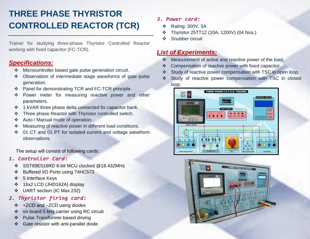
THREE PHASE THYRISTOR
CONTROLLED REACTOR (TCR)
Trainer for studying three-phase Thyristor Controlled Reactor
working with fixed capacitor (FC-TCR).
Specifications: Microcontroller based gate pulse generation circuit.
Observation of intermediate stage waveforms of gate pulse
generation.
Panel for demonstrating TCR and FC-TCR principle.
Power meter for measuring reactive power and other
parameters.
1 kVAR three phase delta connected fix capacitor bank.
Three phase Reactor with Thyristor controlled switch.
Auto / Manual mode of operation.
Measuring of reactive power in different load conditions.
01 CT and 01 PT for isolated current and voltage waveform
observations.
The setup will consist of following cards:
1. Controller Card:
SST89E516RD 8-bit MCU clocked @18.432MHz
Buffered I/O Ports using 74HC573
5 Interface Keys
16x2 LCD (JHD162A) display
UART section (IC Max 232)
2. Thyristor firing card:
+ZCD and –ZCD using diodes
on board 5 kHz carrier using RC circuit
Pulse Transformer based driving
Gate resistor with anti-parallel diode
3. Power card:
Rating: 300V, 5A
Thyristor 25TT12 (10A, 1200V) (04 Nos.)
Snubber circuit
List of Experiments: Measurement of active and reactive power of the load.
Compensation of reactive power with fixed capacitor.
Study of reactive power compensation with TSC in open loop.
Study of reactive power compensation with TSC in closed
loop.
THREE PHASE
THYRISTOR
SWITCHED
CAPACITOR (TSC)
Trainer for studying three-phase Thyristor
Switched Capacitor (TSC) operation.
Specification: Microcontroller based gate pulse
generation circuit.
Observation of intermediate stage
waveforms of gate pulse generation.
Panel for demonstrating TSC
principle.
Power meter is for measuring
reactive power and other
parameters.
3 banks of thyristor switched
capacitor with matching reactive
load.
AC switch (thyristor-diode) for
connecting and disconnecting
capacitor banks.
Auto / Manual Operation.
Measuring of reactive power in
different load conditions.
01 CT and 01 PT for isolated current
and voltage waveform observations.
Principle of TSC is fully
demonstrated with this trainer.
The setup will consist of following cards:
1. Controller Card:
SST89E516RD 8-bit MCU clocked
@18.432MHz
Buffered I/O Ports using 74HC573
5 Interface Keys
16x2 LCD (JHD162A) display
UART section (IC Max 232)
2. Thyristor firing card:
+ZCD and –ZCD using diodes
on board 5 kHz carrier using RC
circuit
Pulse Transformer based driving
Gate resistor with anti-parallel diode
3. Power card:
Rating: 300V, 5A
Thyristor 25TT12 (10A, 1200V) (06
Nos.)
Diode 1N5408 (06 Nos.)
Snubber circuit
List of Experiments: Measurement of active and reactive
power of the load.
Compensation of reactive power with
fixed capacitor.
Study of Thyristor Controlled Reactor
(TCR) operation.
Study of reactive power
compensation with TCR in open
loop.
Study of reactive power
compensation with TCR in close
loop.
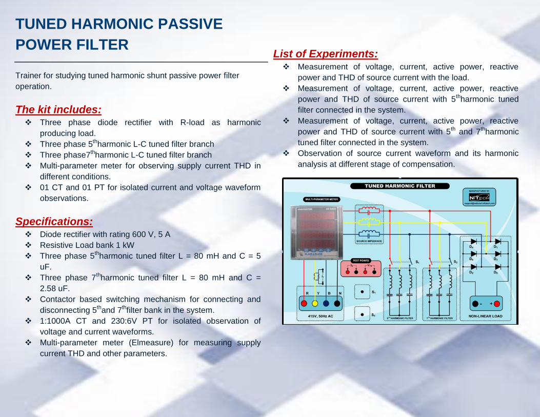
TUNED HARMONIC PASSIVE
POWER FILTER
Trainer for studying tuned harmonic shunt passive power filter
operation.
The kit includes: Three phase diode rectifier with R-load as harmonic
producing load.
Three phase 5thharmonic L-C tuned filter branch
Three phase7thharmonic L-C tuned filter branch
Multi-parameter meter for observing supply current THD in
different conditions.
01 CT and 01 PT for isolated current and voltage waveform
observations.
Specifications: Diode rectifier with rating 600 V, 5 A
Resistive Load bank 1 kW
Three phase 5thharmonic tuned filter L = 80 mH and C = 5
uF.
Three phase 7thharmonic tuned filter L = 80 mH and C =
2.58 uF.
Contactor based switching mechanism for connecting and
disconnecting 5thand 7thfilter bank in the system.
1:1000A CT and 230:6V PT for isolated observation of
voltage and current waveforms.
Multi-parameter meter (Elmeasure) for measuring supply
current THD and other parameters.
List of Experiments: Measurement of voltage, current, active power, reactive
power and THD of source current with the load.
Measurement of voltage, current, active power, reactive
power and THD of source current with 5thharmonic tuned
filter connected in the system.
Measurement of voltage, current, active power, reactive
power and THD of source current with 5th and 7thharmonic
tuned filter connected in the system.
Observation of source current waveform and its harmonic
analysis at different stage of compensation.
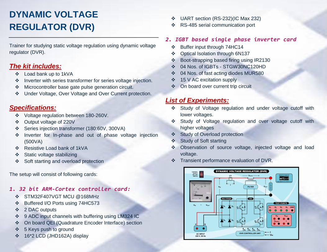
DYNAMIC VOLTAGE
REGULATOR (DVR)
Trainer for studying static voltage regulation using dynamic voltage
regulator (DVR).
The kit includes: Load bank up to 1kVA
Inverter with series transformer for series voltage injection.
Microcontroller base gate pulse generation circuit.
Under Voltage, Over Voltage and Over Current protection.
Specifications: Voltage regulation between 180-260V.
Output voltage of 220V
Series injection transformer (180:60V, 300VA)
Inverter for In-phase and out of phase voltage injection
(500VA)
Resistive Load bank of 1kVA
Static voltage stabilizing
Soft starting and overload protection
The setup will consist of following cards:
1. 32 bit ARM-Cortex controller card:
STM32F407VGT MCU @168MHz
Buffered I/O Ports using 74HC573
2 DAC outputs
9 ADC input channels with buffering using LM324 IC
On board QEI (Quadrature Encoder Interface) section
5 Keys push to ground
16*2 LCD (JHD162A) display
UART section (RS-232)(IC Max 232)
RS-485 serial communication port
2. IGBT based single phase inverter card
Buffer input through 74HC14
Optical Isolation through 6N137
Boot-strapping based firing using IR2130
04 Nos. of IGBTs - STGW30NC120HD
04 Nos. of fast acting diodes MUR580
15 V AC excitation supply
On board over current trip circuit
List of Experiments: Study of Voltage regulation and under voltage cutoff with
lower voltages.
Study of Voltage regulation and over voltage cutoff with
higher voltages
Study of Overload protection
Study of Soft starting
Observation of source voltage, injected voltage and load
voltage.
Transient performance evaluation of DVR.
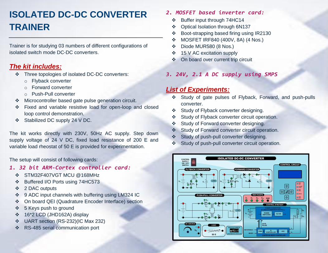
ISOLATED DC-DC CONVERTER
TRAINER
Trainer is for studying 03 numbers of different configurations of
isolated switch mode DC-DC converters.
The kit includes: Three topologies of isolated DC-DC converters:
o Flyback converter
o Forward converter
o Push-Pull converter
Microcontroller based gate pulse generation circuit.
Fixed and variable resistive load for open-loop and closed
loop control demonstration.
Stabilized DC supply 24 V DC.
The kit works directly with 230V, 50Hz AC supply. Step down
supply voltage of 24 V DC, fixed load resistance of 200 E and
variable load rheostat of 50 E is provided for experimentation.
The setup will consist of following cards:
1. 32 bit ARM-Cortex controller card:
STM32F407VGT MCU @168MHz
Buffered I/O Ports using 74HC573
2 DAC outputs
9 ADC input channels with buffering using LM324 IC
On board QEI (Quadrature Encoder Interface) section
5 Keys push to ground
16*2 LCD (JHD162A) display
UART section (RS-232)(IC Max 232)
RS-485 serial communication port
2. MOSFET based inverter card:
Buffer input through 74HC14
Optical Isolation through 6N137
Boot-strapping based firing using IR2130
MOSFET IRF840 (400V, 8A) (4 Nos.)
Diode MUR580 (8 Nos.)
15 V AC excitation supply
On board over current trip circuit
3. 24V, 2.1 A DC supply using SMPS
List of Experiments: Study of gate pulses of Flyback, Forward, and push-pulls
converter.
Study of Flyback converter designing.
Study of Flyback converter circuit operation.
Study of Forward converter designing.
Study of Forward converter circuit operation.
Study of push-pull converter designing.
Study of push-pull converter circuit operation.

Typical waveforms:
Following are the waveforms observed during the operation.
(i) Waveforms of forward converter operation:
(ii) Waveforms of push-pull converter operation:
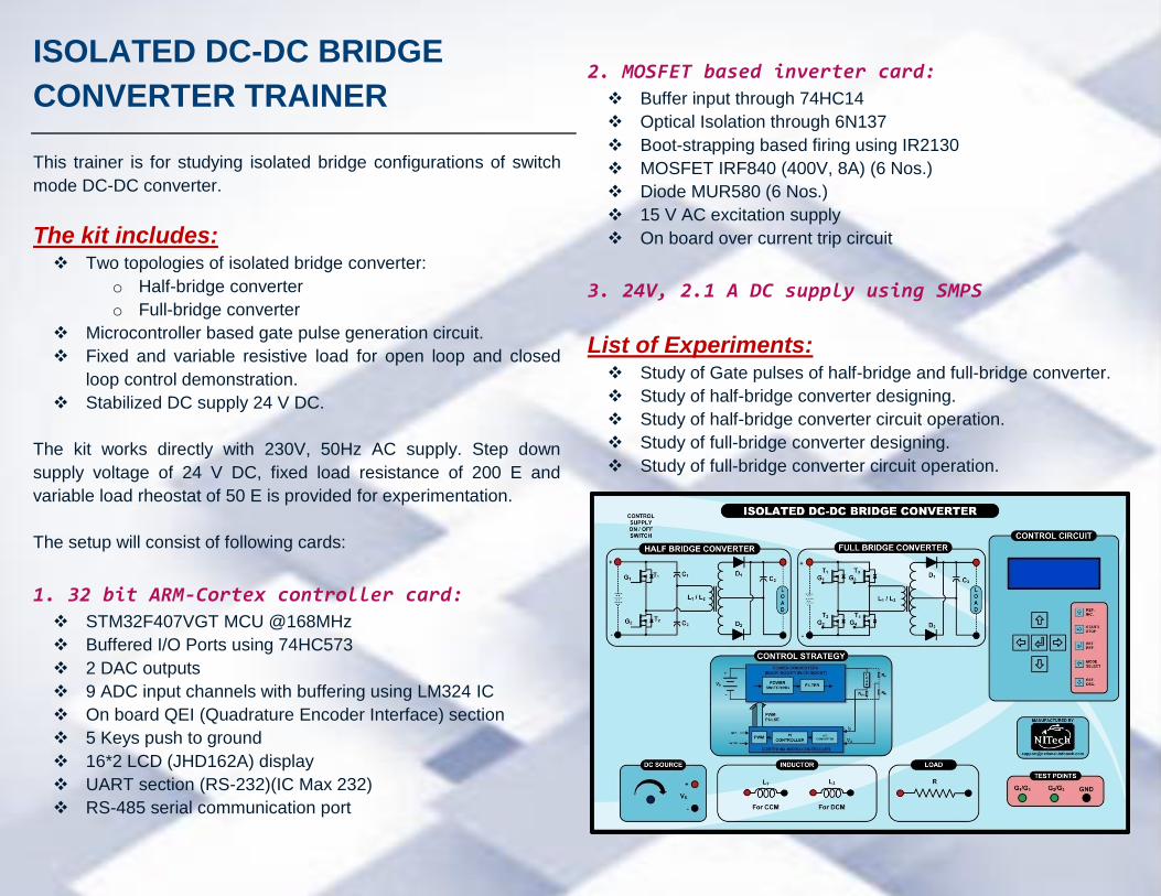
ISOLATED DC-DC BRIDGE
CONVERTER TRAINER
This trainer is for studying isolated bridge configurations of switch
mode DC-DC converter.
The kit includes: Two topologies of isolated bridge converter:
o Half-bridge converter
o Full-bridge converter
Microcontroller based gate pulse generation circuit.
Fixed and variable resistive load for open loop and closed
loop control demonstration.
Stabilized DC supply 24 V DC.
The kit works directly with 230V, 50Hz AC supply. Step down
supply voltage of 24 V DC, fixed load resistance of 200 E and
variable load rheostat of 50 E is provided for experimentation.
The setup will consist of following cards:
1. 32 bit ARM-Cortex controller card:
STM32F407VGT MCU @168MHz
Buffered I/O Ports using 74HC573
2 DAC outputs
9 ADC input channels with buffering using LM324 IC
On board QEI (Quadrature Encoder Interface) section
5 Keys push to ground
16*2 LCD (JHD162A) display
UART section (RS-232)(IC Max 232)
RS-485 serial communication port
2. MOSFET based inverter card:
Buffer input through 74HC14
Optical Isolation through 6N137
Boot-strapping based firing using IR2130
MOSFET IRF840 (400V, 8A) (6 Nos.)
Diode MUR580 (6 Nos.)
15 V AC excitation supply
On board over current trip circuit
3. 24V, 2.1 A DC supply using SMPS
List of Experiments: Study of Gate pulses of half-bridge and full-bridge converter.
Study of half-bridge converter designing.
Study of half-bridge converter circuit operation.
Study of full-bridge converter designing.
Study of full-bridge converter circuit operation.

THREE PHASE PWM
RECTIFIER
This trainer is for studying Three Phase
PWM Rectifier Operation.
The kit includes: The experiment setup consists of three-
phase PWM rectifier, 32-bit Cortex M4 ARM
microcontroller based controller for gate
pulse generation, and load. Test points for
current and voltage waveform observation
across different elements are provided.
Detailed features and specifications are as
listed below:
Isolated 110V, 50Hz three-phase AC
input voltage.
Boost Converter with 220V, 2.0A
capacity.
Current Transformer for current
waveform observation.
Digital control circuit implementation
using latest Cortex M4 ARM 32-bit
microcontroller (STM32F407VG).
Slow outer voltage control loop
working at 100 µSec and fast inner
current loop working at 10 µSec.
Two different current control method,
Average Current Control and
Hysteresis Current Control can be
studied.
Accessibility to monitor the gate
pulses of the boost converter.
Rugged packaging with plug and
socket type banana connector.
32 bit ARM-Cortex controller card:
STM32F407VGT MCU @168MHz
Buffered I/O Ports using 74HC573
2 DAC outputs
9 ADC input channels with buffering
using LM324 IC
On board QEI (Quadrature Encoder
Interface) section
5 Keys push to ground
16*2 LCD (JHD162A) display
UART section (RS-232)(IC Max 232)
RS-485 serial communication port
The pictorial view of the front panel of the
kit is shown below.
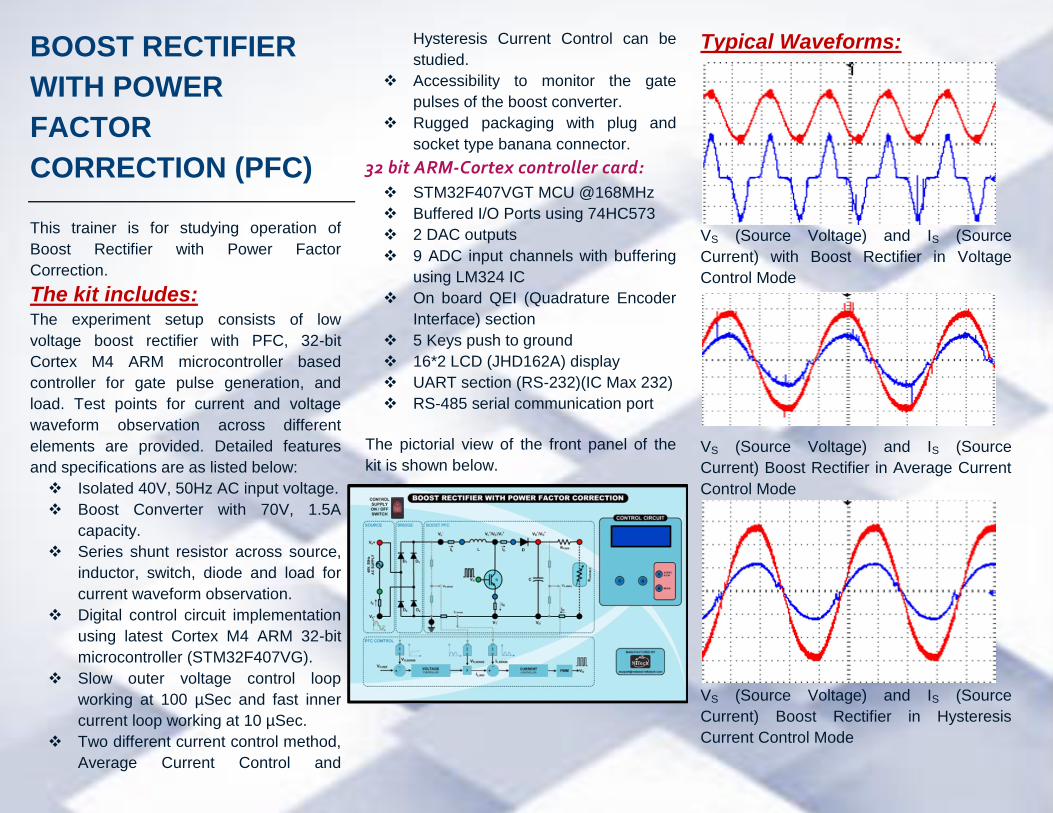
Typical Waveforms: VS (Source Voltage) and IS (Source
Current) Boost Rectifier in Average Current
Control Mode
VS (Source Voltage) and IS (Source
Current) Boost Rectifier in Hysteresis
Control Mode
VS (Source Voltage) and IS (Source
Current) Boost Rectifier in Peak Current
Control Mode
BOOST RECTIFIER
WITH POWER
FACTOR
CORRECTION (PFC)
This trainer is for studying operation of
Boost Rectifier with Power Factor
Correction.
The kit includes: The experiment setup consists of low
voltage boost rectifier with PFC, 32-bit
Cortex M4 ARM microcontroller based
controller for gate pulse generation, and
load. Test points for current and voltage
waveform observation across different
elements are provided. Detailed features
and specifications are as listed below:
Isolated 40V, 50Hz AC input voltage.
Boost Converter with 70V, 1.5A
capacity.
Series shunt resistor across source,
inductor, switch, diode and load for
current waveform observation.
Digital control circuit implementation
using latest Cortex M4 ARM 32-bit
microcontroller (STM32F407VG).
Slow outer voltage control loop
working at 100 µSec and fast inner
current loop working at 10 µSec.
Two different current control method,
Average Current Control and
Hysteresis Current Control can be
studied.
Accessibility to monitor the gate
pulses of the boost converter.
Rugged packaging with plug and
socket type banana connector.
32 bit ARM-Cortex controller card:
STM32F407VGT MCU @168MHz
Buffered I/O Ports using 74HC573
2 DAC outputs
9 ADC input channels with buffering
using LM324 IC
On board QEI (Quadrature Encoder
Interface) section
5 Keys push to ground
16*2 LCD (JHD162A) display
UART section (RS-232)(IC Max 232)
RS-485 serial communication port
The pictorial view of the front panel of the
kit is shown below.
Typical Waveforms:
VS (Source Voltage) and IS (Source
Current) with Boost Rectifier in Voltage
Control Mode
VS (Source Voltage) and IS (Source
Current) Boost Rectifier in Average Current
Control Mode
VS (Source Voltage) and IS (Source
Current) Boost Rectifier in Hysteresis
Current Control Mode
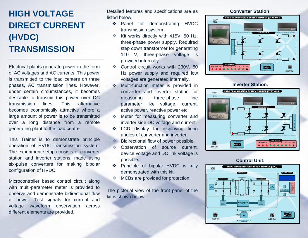
HIGH VOLTAGE
DIRECT CURRENT
(HVDC)
TRANSMISSION
Electrical plants generate power in the form
of AC voltages and AC currents. This power
is transmitted to the load centers on three
phases, AC transmission lines. However,
under certain circumstances, it becomes
desirable to transmit this power over DC
transmission lines. This alternative
becomes economically attractive where a
large amount of power is to be transmitted
over a long distance from a remote
generating plant to the load centre.
This Trainer is to demonstrate principle
operation of HVDC transmission system.
The experiment setup consists of converter
station and inverter stations, made using
six-pulse converters for making bipolar
configuration of HVDC.
Microcontroller based control circuit along
with multi-parameter meter is provided to
observe and demonstrate bidirectional flow
of power. Test signals for current and
voltage waveform observation across
different elements are provided.
Detailed features and specifications are as
listed below:
Panel for demonstrating HVDC
transmission system.
Kit works directly with 415V, 50 Hz,
three-phase power supply. Required
step down transformer for generating
110 V, three-phase voltage is
provided internally.
Control circuit works with 230V, 50
Hz power supply and required low
voltages are generated internally.
Multi-function meter is provided in
converter and inverter station for
measuring three-phase line
parameter like voltage, current,
active power, reactive power etc.
Meter for measuring converter and
inverter side DC voltage and current.
LCD display for displaying firing
angles of converter and inverter.
Bidirectional flow of power possible.
Observation of source current,
device voltage and DC link voltage is
possible.
Principle of bipolar HVDC is fully
demonstrated with this kit.
MCBs are provided for protection.
The pictorial view of the front panel of the
kit is shown below.
Converter Station:
Inverter Station:
Control Unit:

Typical Waveforms:
Waveforms of output voltage (Vdc) and input AC current of converter
station (for Firing angle 30°)
Waveforms of voltage across device and input AC current of
converter station (for Firing angle 15°)
Waveforms of output voltage (Vdc) and voltage across device of
converter station (for Firing angle 15°)
Waveform of input AC current of converter station and inverter station
(for Firing angle 15°)