national radio astronomy observatory · the 45-ft telescope position control and monitor facilities...
TRANSCRIPT

NATIONAL RADIO ASTRONOMY OBSERVATORY
GREEN BANK) WEST VIRGINIA
ELECTRONICS DIVISION INTERNAL REPORT No. 149
NRAO 45-FOOT TELESCOPE
DIGITAL POSITION CONTROL AND READOUT SYSTEM
J. RAY HALLMAN
NOVERMBER 1974
NUMBER OF COPIES: 150

NRAO 45-FOOT TELESCOPE DIGITAL POSITION CONTROL AND READOUT SYSTEM
J. Ray Hallman
The digital position control and readout (DPCAR) electronic system provides
the 45-ft telescope position control and monitor facilities used to accurately
point the telescope. The basic system contains the stand-alone calculator con-
trol circuit cards 24, 25, and 26 (described in EDIR #128), the inductosyn posi-
tion readout system cards 27 and 28 (contributed by Ron Weimer), and the digital
position servo control cards 29, 30, 31, and 32. Also described in this EDIR is
a test fixture (useful in testing the telescope response) and the analog control
panel circuits that were added to permit monitoring of the telescope drive motor
currents.
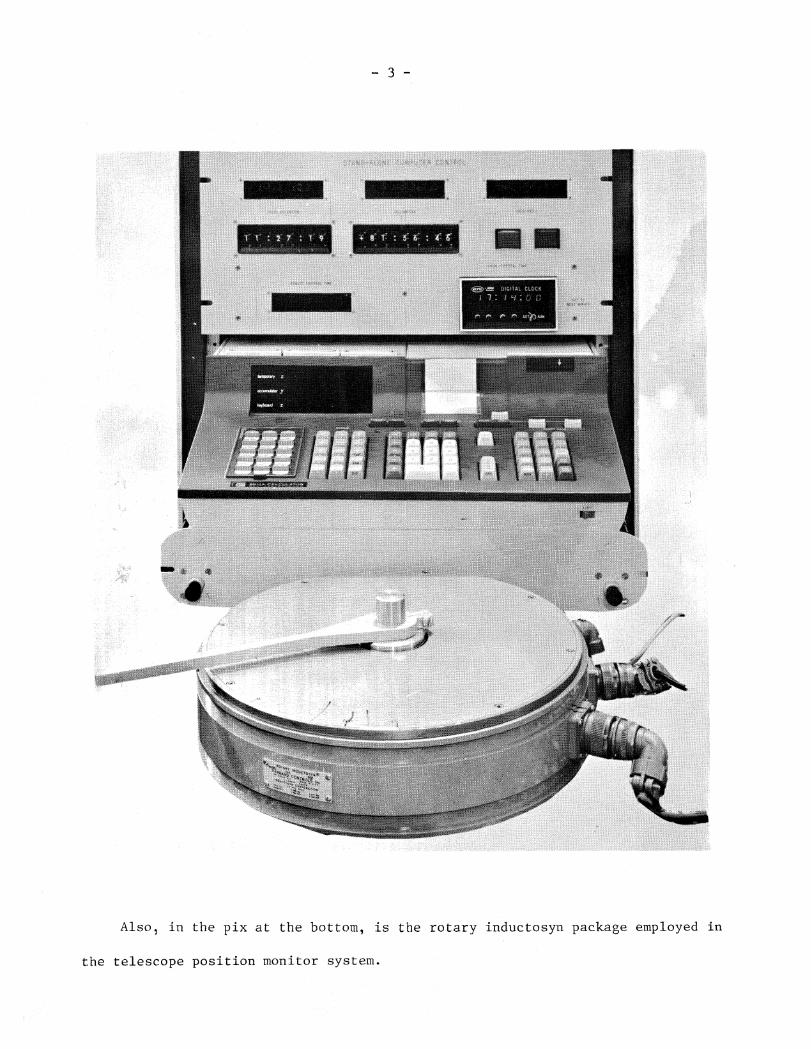
A picture of the DPCAR front panel is presented below.
In the pix, coarse and fine indicators display the actual 11 and 12 bits
respectively of the inductosyn converter logic outputs when the cross-over con-
trol is in position "0". The "crossover"control provides an electronic means
of adjusting the offset between the "fine" and "coarse" (1 speed and 256 speed)
resolvers. The crossover control adds the displayed value to the most significant

octal digit of the "fine" outputs. The "composite" position displays indicate
the octal value of the position readout after logical combination of the "fine"
and "coarse" values and after a digital offset calibration value is added to the
position values. The "offset cal" enables electronically the azimuth and eleva-
tion position readout inductosyns to be zeroed without the necessity of adjusting,
mechanically, the resolvers. The yellow "initialize position readout" push-
button resets the inductosyn converter counting system. This is done automatically
whenever a computer update error occurs via the digital data link system. The
button lights during a reset sequence.
The position servo loop status indicators display the mode of the digital
servo control circuits which may be either + full scale, - full scale, or linear
(D/A) mode. Normal operation is "linear" but during observing source changes,
usually the mode changes to full scale during slew. This digital control is
connected via DAC's to the analog servo control system described in EDIR #127.
A picture of the "stand alone" computer control is shown on the next page.
,1°10 fTAL CLOCK
:
-11111111111AMap
MEV ;.:110124.
01109:041.MSOKMO'MAKVIVOVWS",".14011"4010111060411660,044°
Also, in the pix at the bottom, is the rotary inductosyn package employed in
the telescope position monitor system.

-ZiEW.V,
AlL51
WA*,
The DPCAR logic circuits are assembled in the top-most 7-inch rack-mounted
drawer, a picture of which is presented showing the "insides".
The "box" rolls out on slides when careful attention is given to the rear
cables. The meters provide monitoring facilities of the 15 V DC and +5 V DC
power supplies.
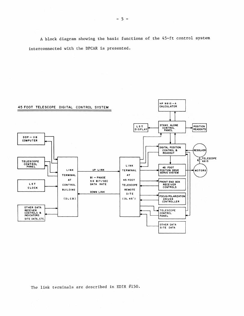
45 FOOT TELESCOPE DIGITAL CONTROL SYSTEM
LSTDISPLAY
HP 9810-ACALCULATOR
STAND ALONECONTROL
PANEL1--110 POSITION
READOUTS
FD DP -- 116COMPUTER
TELESCOPECONTROL
PANEL
LSTC LOCK
OTHER DATA RECEIVERCONTROLS BINDICATORS rSITE DATA, ETC.
e-,TELESCOPEAXIS
LINK 45 FOOT
LINK UP LINK TERMINAL POSITION DRIVESERVO SYSTEM
TERMINAL ATBI - PHASE
AT 5K BIT/SEC 45 FOOTFRONT END BOX
CONTROL DATA RATE TELESCOPE RECEIVERCONTROLS
BUILDINGDOWN LINK
REMOTESITE
FOCUS/ POLARIZATIONDRIVER
CONTROLLER
TELESCOPECONTROLPANEL
( DL 45')( D L C B )
A block diagram showing the basic functions of the 45-ft control system
interconnected with the DPCAR is presented.
OTHER DATASITE DATA
The link terminals are described in EDIR #150.

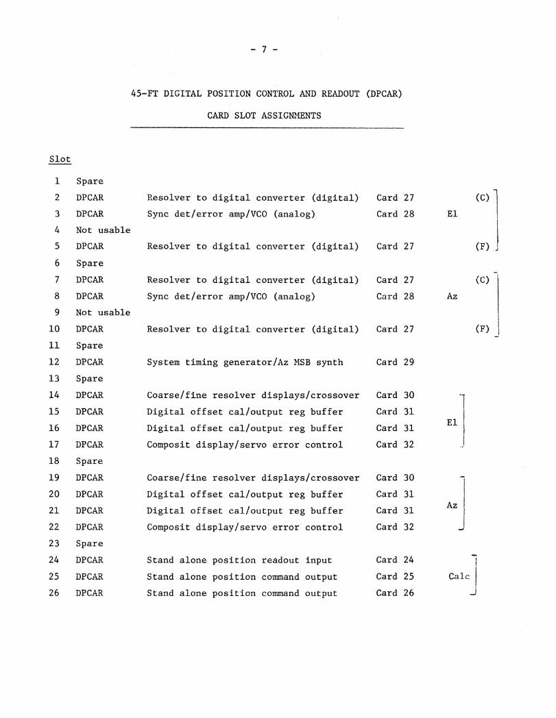
A picture of the DPCAR card file is presented showing the electronic card
complement and locations.
There are 26 slots of which 18 are used. There is some redundancy result-
ing in only 9 different logic cards required for spares. Note the digital dis-
play wiring in the pix. The displays are connected using a multiplexing scheme
resulting in great saving of cabling and wiring.
(C)
El
(F)
7
45-FT DIGITAL POSITION CONTROL AND READOUT (DPCAR)
CARD SLOT ASSIGNMENTS
Slot
1 Spare
2 DPCAR
3 DPCAR
4 Not usable
5 DPCAR
6 Spare
7 DPCAR
8 DPCAR
9 Not usable
10 DPCAR
11 Spare
12 DPCAR
13 Spare
14 DPCAR
15 DPCAR
16 DPCAR
17 DPCAR
18 Spare
19 DPCAR
20 DPCAR
21 DPCAR
22 DPCAR
23 Spare
24 DPCAR
25 DPCAR
26 DPCAR
Resolver to digital converter (digital) Card 27
Sync det/error amp/VCO (analog) Card 28
Resolver to digital converter (digital) Card 27
Resolver to digital converter (digital) Card 27
Sync det/error amp/VCO (analog) Card 28
Resolver to digital converter (digital) Card 27
System timing generator/Az MSB synth Card 29
Coarse/ fine resolver displays/crossover Card 30
Digital offset cal/output reg buffer Card 31
Digital offset cal/output reg buffer Card 31
Composit display/servo error control Card 32
Coarse/fine resolver displays/crossover Card 30
Digital offset cal/output reg buffer Card 31
Digital offset cal/output reg buffer Card 31
Composit display/servo error control Card 32
Stand alone position readout input Card 24
Stand alone position command output Card 25
Stand alone position command output Card 26
Calc

8
Description of Circuits
Cards #24, 25, and 26: EDIR #128 describes these circuits.
Card #27: The schematic showing the inductosyn converter digital logic is
presented below.
"0" ADVANCES ERROR OF REF+ V
7161411013111741-104I E-2)02.,
3 ID:,8 8281 8281 56
REF13
91 13 I+vCLCK 113 CC •
REF2V8M
9 +V RS113
8281
1 0 13 11 i4 15
+V RS82 3 6 I2
REF/4 CAN CUP8281
I000pF + vT
UP 9104 CUP
DD45 2 DD 2127474 6 CDN3U/D 4M --- UP 6MM 74193
7+V
+V4
74S746
LL
13 12+V4
7 4 51126
13 543 312
RS874S7422
+VLL7419 313 15
1213+ V +V10 4 5
31:1CLCK
124s112 745112 74511213 2
67419 3+V1414
RSC4
RESET
BORROW CARRY+V8M
VCO IN 9+V 2-
5
74511274511244M6
12 7REF/4
Tio
2,46,810,12
I, 35, 9
"' 13 1D-15 114
+V
2,4 33OL 2[00,3
3, 5 6,810,124
9,11,1374 74 AA 34M >IL 15
2,4 106,810,12
MM 8 5113
+V5SLOTC 2,41,3
5,9H,I3
PHASEWITH-
=110 RES. II ,36,810,129
10+G RSC
X:XXI 0534K 8
52K /24 C-7 2
14 PIN PROGRAMMABLEPLUGS I I 113
+V FiSCV
45' POSITION READOUT , RESOLVER TO DIGITAL CONVERVTER CARD No. 27DIGITAL COUNTER/DRIVER CIRCUITS
The converter system crystal time base is in the upper left corner. The
reference counter string which drives the synchronous detector (card 28) is
along the top.

The synchronizing (reset) logic is in the middle left side of the drawing.
The VCO input logic is in the lower left which drives the sin and cos generator
counters in the middle and lower middle of the schematic. The counters control
the sin and cos inductosyn winding drivers in the lower right corner. Calibra-
tion circuits comprising two balance pots are mounted in the chassis behind the
card sockets. The binary output is generated by the up/down counters in the
middle right side of the schematic which count incrementally and synchronously
with the sin and cos counters.
Position resolution is adjusted by changing the straps on a programmable
plug located in slot "C" on the digital card #27.
The basic principle of operation is as follows: Proportional sin and cos
signals are generated by the digital counting logic of card #27 which drive the
rotary inductosyn in a reverse (non-conventional) direction. A single output
from the inductosyn rotor is filtered, amplified, synchronously detected, fil-
tered, and amplified providing error magnitude and direction signals which con-
trol the above-mentioned digital counting logic, resulting in a negative feed-
back loop circuit. A VCO with it's "dead zone" thresholds operates from the
magnitude signal to "speed up" the converter counting logic during position
slewing. Also, an up/down counter operates incrementally from these error sig-
nals via control logic providing the 12-bit position output data for "outside
world" utilization circuits.

1 M
DOT 3610K: 10K COARSE- LPM15000
FINE-LPM6000 REF
REF
+510K
10KX- 20 = +15Y-21 = -15B-2 = +5A-1, Z- 2 2 =GND
20K10K
Ii
MA,1N914
100K
5K 3
10K
10 K
+157 6
4 1 N914
VCO5.1K* +V OUTMA•
15
OUT
+551K* 560pF
RESISTORS = 1%, * = 5%
OP AMPS = 741
1N4733
1 K
BN
420K -15
150KLPM 6000
10K 1 3A --/V00---o o--2
20K 2
3
1.24 M
+157
6
- 10 -
Card 28: The principles of the analog card #28 are discussed under card
#27. The schematic shows the input port (upper left) for the inductosyn rotor
signal. The transformer provides common mode noise rejection. Along the top,
45' POSITION READOUT, RESOLVER TO DIGITAL COMPUTER CARD No.28ANALOG CIRCUITS/ SYNC. DET. / ERROR AMP. /VCO
the filter and amplifier string drive the synchronous detector (upper right)
which is filtered (lower left) and sliced, providing the up/down output pin 7
(middle drawing). The VCO threshold and amplifier circuits (lower middle) and
VCO (lower right) provide a frequency output aiding in converting a rapidly
changing position input to the inductosyn.

PP 7402PP
JJ
8280A
12 13
U.SYNC
AZIMuTH180° EBITINPUT
SPARES:GND
GND
45 LL)D1--
UHP 507II
11 1/4 SECOND
+5 UHP507 11K
+5
12
A complete position readout conversion system for one axis requires two
digital logic cards #27 and one analog card #28.
Card 29: The DPCAR system timing generator and "extra" logic card #29 is
drawn below.
+VA I K
14 13T 13T 1 256KHz R SOSC JJ -C2 RFRBB 8280 8280
C D B C D C1 A9
1 2 1 2 1912.1218.51.2 KM.
5 12KH.+V
7400
2.56KHz
10 DISPLAYCLOCK
AS 2
10
T Q7474 _
C R Q
13
7400
4 AS
8563
14 I
POSITIONREADOUTSTROBE
5
IK
AFF
8563 c
INDUCTOSYNHOLD
6PP
8H90 11-
43
2 NN9
8
-tr
= OPEN WHEN 270° PASSED
+15V
2.5K8820 10
10
PP
7400
AA
+5V
DD 7 4-2–NN
13 1a<'-'+VR Q 10
S 9602 I LI 2.
+5v +15,„ VIA LINK .22 .22 lni 50/50Us
+V +15V
+V
5.IK
74009
13
MM
C L D8280
REMOTE
•
S A C2
12
4
R S A C2
M D8280
+v I51-111. .< +V
NN- 3 <--jL
12 8
12
13
R S A C2
C J D8280
DD9602 5-
12
5
3
C K D
MS
5
8288
S DD9602 5
+V
1,4
31K
+5RSS
C S D12 C
13
82889602.s
7400MM
IK
+5' UHP507LL 3
6 2 LL
1312 AS
PP
HPCALCULATOR
MTE RUPT
REG8890
LOAD
10 Op,
EEs,
+5
S 2 = OPEN WHEN 90° PASSED+15
2.5K 8820
S2EE
AZIMUTH360°BIT OUT
LNO0C .A L
SWITCH
I L* J.2_1(,).A,._.< +v
.22
INITIALIZEPOSITIONREADOUTLAMP
RESETINDUCTOSYNLOGIC
–n– ms( ONE CARD BOTH AXIS TAKE UP TWO CARD SLOTS I
DIGITAL POSITION COMMAND & CONTROL
SYSTEM TIMING GENERATOR /AZIMUTH MSB SYNTHESIZER CARD NO. 29 — SLOT NO.12
The system time base (upper left corner) drives the timing generator string
(top) which provides the display clock (pin H) to the front panel mounted digital
displays. Also the "assured" readout system strobe logic (upper middle of drawing)

- 12-
is synchronized to the data link which is synchronized to the control building
sidereal clock. Pin 6 is the link sink input to the assured strobe which operates
at 10 Hz with output at pin J. Also an interrupt signal to the "stand alone"
calculator signals it when position data is valid. Pin L strobes the position
readout data register located on card #31.
The telescope azimuth axis travels through a position range greater than
3600 of travel and therefore requires an indicator bit to signal when the tele-
scope has passed 3600 of travel. The bit is "synthesized" synchronously with the
position encoder 1800 bit by means of two micro rocker switches mounted on the
telescope pedestal. The logic associated with the 3600 bit is in the left middle
of the drawing with the output at pin N.
A divider chain providing a reset (initialize signal to the inductosyn sys-
tem) every 10 minutes is in the lower middle of the drawing with an output at
pin "R-7", which is "ORed" with the local yellow "initialize" switch on the
front panel with signal input at pin 16.
The logic in the lower middle of the schematic receives the "computer up-
date error signal" from the data link and updates the position readout via the
"one shots" and driver circuits in the lower digit of the drawing.

MSB
CMS'
tflOC4 tF7
F4
A415 6 9 10[11114
C O 1 2 3 4 5 6 718• MM
OUT
1.
A DM8210
CII 52I F5
1"3
1F-11
3 t4 5 6 9 1G 111121
4
4
FINE TRUESELECTDISPLAYC 2COARSE
5 13 B SCAN
LOB
14 A FIRST
— 13 —
Card 30: The electronics in card 30 provide automatic crossover correction
for the "coarse" and "fine" functions of the two speed position readout system,
thus providing a singlecompositemontonic position output. As shown in schematic
#30, the crossover logic comprises binary adders at the top of the drawing which
add the three most signficant bits of the "fine" data to the "coarse" position data.
69
BITMSB CI
2[jE.-- C2
F--- C33 [1.3j
C44 [1_4-,
COARSE
1NDUCTOSYN 5 [15 -4 F- C5
F- C7
.Fd —CB
9L91C9
r-- CIOMP°J
11{21 j— C II
I2[2 — C12
510Buss ,[ TRUE +V
FALSE
A 111CROSSOVERRANGE B 6ADJ.
111 II 7
NC— 54, B 2 B3 64
A,63
A
- 7483 62
Co
13
F4
FINEINDUCTION F5INPUT
FE
9 LS8 's „COMPOSITE L2POSITION
8 F 8
9 LAid--> F9
IO j F 10
I1 F 1 >F1I
r Z F 12
4:1c
SPARES
H
H H> 4
i-3—[HH >12
S3
Si
I NCNC —
8H90
S2
SI 5
H1-1
II' 7 41161NC NC
C ° C4 €4
AA
' 7483 !-3- 2 FFSi
82 '3 8:1
+vNC
13 114
HH
--NC2--W6
Co C4 154 E4 227483 6
J.2AI NN 9 NC
16
B48382E11
III‘ -Z-7
44 E4
A: 7483 E:- 61 PP E l 9
134 83 82 Eil4 7 11113
13 14
15
2
2
C0 1 2 3 4 5 6 7
• LLutJT
A DM8210
C12 53C9A Ap6
C68 A 9
C3 6 FI2
3 4 9 1
c 0
•
3 4 6 7
A DM8210K K 8
H COMPOST
POSITIONJj
8
BLUE AUGATCCNNECTOR
DISPLAYDATABUSS
INPUT , 1-- C66 16
+51 B12 1 14,PWR. moin
GNDI A 1 GND
+v
12
NC= NO CONNECTION
FOR 7483s - 16 PIN 1 KVCC.5GND.12
OTHER 1 's ARE 14 PINVcc = 14GNI) . 7
DIGITAL
2 9
A
EE82 81
12CI
8
r1-1 DISPLAYCLOCK
POSITION CONTROL & READOUT
13,D D
lOrnH
.0022
25K HzL PP
2.4K3.9K 71ST
+V 9 11_21V,,c
GND]
-u-
COARSE/ FINE DISPLAYS 81 CROSSOVER CONTROL CARD NC. 30

- 14 -
The adder chip "FF" subtracts the two least significant bits of "coarse" data
from the two most significant bits of "fine" data. The net result is that any
variation due to relative error between the coarse and fine speed resolver is
cancelled. Adder chip "Jr calibrates the crossover circuits to the most opti-
mum range of operation by adding an offset (selected by the crossover adjust
switch) to the "fine" position data which zero's the "fine" resolver to the
"coarse" resolver.
The circuits in the lower right corner of the drawing provide multiplexed
character serial data to the "coarse" and "fine" digital displays on the front
panel.

- 15-
TABLE I
CROSSOVER VALUES TO ADD TO C TO FORCE = TO F = 200 CTS COMPOSITE
0.5 = 1000 CTS fine or (2 CTS) coarse on the respective display.(No odd CTS on coarse.)
Optimum RangeChosen
-0.5 +0.5C9C10-F1F2ERROR 4.F1F2 = C9C10JPIFF+3+2+10
-1-2-3
-2.51-1.5
+3+2 +2
+1 +1
1+3+2 +2
+1 +1
+1.51+2.51+3.5
•■■••
3.5
-4 4 I 1 0-5 3 +3-6 +2 +2-7 +1 +1
■•■•
1 Period of FineEquivalent
8000 CTS Fine (octal)1000 CTS Composite (octal)10) Coarse
8
(Relative)Counts DFN
Fine Coarse Display F 1 = C 9 4000 - 10 Fine = Fine + CrossoverF2 = C10 2000 - 4 1 Crossover CT =F3 = C 11 1000 - 2 1000 CTS of Fine
= 200 CTS of CompositeCoarse = Coarse
rpmposite = Coarse ±,(Fine + Crossover - Coarse)+ Coarse.]
VALUES BELOW AND TO RIGHT OF DOTTED LINE ARE REDUNDANT.
To adjust the crossover control, move telescope untilcoarse readout is changing from XX76-AXX00 and adjustcrossover control for the nearest fine indication of2400. The crossover control causes an increment of1000 counts of fine for each increment of the cross-over switch. Adjustment of the crossover may alterthe digital offset cal of the encoders. This shouldbe rechecked.
+V
381Ta
I/1
2/12
7408
A
9
12
+VGND
- 16 -
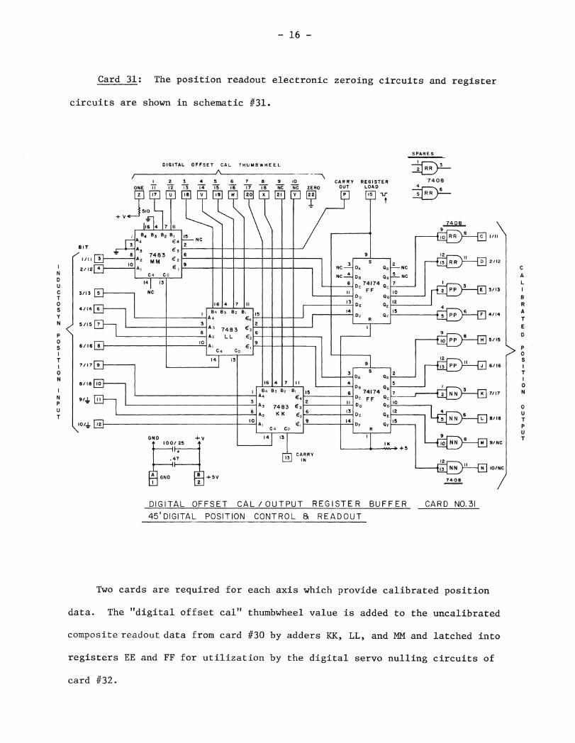
Card 31: The position readout electronic zeroing circuits and register
circuits are shown in schematic #31.
SPARES
DIGITAL OFFSET CAL THUMBWHEE L
A-------------2 312 13
ILI
4 514 15
6 7 8i6 17 18
9 10NC NC ZERO
Ell
CARRYOUT
REGISTERLOAD176-1
7408ONE II
510
16 415 4 83 8 2 B
1 15A4 E4
7-A, €3
7483A2 MM €2
NC
8
FF 10 3/13 I 1O D QD
12DE OE14 15 4/14C. F QF
A
121
QA2
A
DB QB5
10
6 715 74174DC FF Qc2 IIDD OD
1013 2
NN
0
14DE OE
5OF
A QA
QBDc 74174 Qc
3/13
04/14
5M5
06/16
1
1 7/170
8/18 101
764 83 B2 BI
A4 €4
3 7483 63LL 2
C4 CO El
14 13
8
9
16 4 784 8 3 8 2 81
A464
A3 7483 €3A, K K
A,C4 Co
—lit 13
E C4 CO
16 4
26
15
CARRYIN
+5V
1K+ 5
12NN
7408
DIGITAL OFFSET CAL/OUTPUT REGISTER BUFFER CARD N0,3145 I DIGITAL POSITION CONTROL & READOUT
Two cards are required for each axis which provide calibrated position
data. The "digital offset cal" thumbwheel value is added to the uncalibrated
composite readout data from card #30 by adders KK, LL, and MM and latched into
registers EE and FF for utilization by the digital servo nulling circuits of
card #32.

- 17 -
-P55 PC 5 NULLNC
'at 8H90A483 7
e 15A 2 4 €3 2
A I 8 E2:4 3 El
ZB1 Co
NC14f
X=Y=I IF A=B0=1 IF A>13Y=1 1F 6<B54 C4
A3 7 E4A2 4 €3Ai 8 E2B4 3 E.B3
NN
Bi
134-
Bc
±Y E 411Y--16
6 91_
Y8 3 0 B3 T'---1•3A2 0 B2A, V B, —
ST 81
A-513
COMMAND -FS
A<1313IS ALL O's TO DAC
COMMAND + FS12
4107IK 11
7
13
507NC
14f
7483
FE
131
BIT12 15_I3 J
+53 153157483
a 2 2136 6
8200
23
9I 4
1T1327 410
4• 5 171• 6 J
7 Ej620
w
1 6 20 1
1/2W
1.
138200
+ 51
mBLUE SOCKET
I ® I
MARK -"SERVOSTATUS"LAMPS
4+5K4--
15,
H' Y43 Y3
EEB C
0
• 8
m .iLN
2IK4 6
8 9
>84MM7
N.0,ZERO k REDTEST / P. B.
7400
2
R
s15 2
7 2 5T 4 10U 8 9 13
4 3
7 LL
NONINVERTING -15 +158H90
6 ZERO74
8
6
287
DD12
• 13 T 1415
ZERO
BIT
ADJ.
el 8 23 DAC 12 QZ
IC + V +5HH JJPP RR GNI)
5 GOD
vw 4.1-xsr .12-
15 25
7
12LS 8
NOD
20
10
7483
KK
74
87
CC
3 15 16
OU27 I
C
SERVOPOSITION6 9 17
DRILL HOLESFOR PINS8 & 2113 12 18 ERROR
OUT4 BIPOLAROFFSET
IA E171819 Z
+5 114._,A<A.,... 1
N.C.i-CFKNTW314 1 51 61 91.1 421 0 I 2 3 4 5 6 7
8 X OUA DM8210
r BITI El---0.132 —C3 Cg D4 —E5 EI • F6 —H7 El J8 —K9 0 .L10 ftJ—M1112 R13 Jj • S1415 EI u16 D' •• V17 • W18 1-11. X
Y
4
0
A
0
N.C.+DHLRUX31 41 51 61 91101 111121
c 0 I 2 3 4 5 6 7
8 W OUA DM 8210
N.C.BEJMSVY
31 41 51 61 91101111121
c 0 I 2 3 4 5 6 7
8 OUTA DM821013
R S828
IDDISPLAYCLOCK 8
ID9 A
STrnH12
2.4K 3.96.002 22 8H90+0 9 10 Vcc
5 II GND1GND •,U.HP 50 7981190 7400 2
LL--7>2 Dog IgiDo_
SPARES
SPECIAL BLUE AUGATCONNECTOR - — —
MARK "COMPOSIT DISPLAY"
COMPOSITE DISPLAY AND SERVO ERROR CONTROL CARD 32

SOLIDTOGGLE STATESWITCH SWITCHOFF ON 100A
I • • AAArriAFUSE
3WIREACLINE
1.1•11111••
LAMBDA LYTE
5152 POWER
SUPPLY
+15+5
GND
-15
- 18 -
Card 32: Card 32 is a digital subtractor circuit which provides high gain,
thus limiting the output providing a linear output via a D/A converter (DAC 12
QZ) over a narrow range of difference between the position command and position
readout inputs.
Also, circuits on the card (bottom of drawing) provide multiplexed octal
data to the composite displays on the front panel. The circuit at the middle
right controls the servo status indicators.
The Power Control Circuit: The power supplies used in this project are
the switching regulator type which employ a full wave rectifier bridge directly
across the primary power line. The bridge feeds a large capacitor such that
under certain conditions when the power switch is turned on the contacts stick
(weld), thus rendering the power switch ineffective. The power control circuit
eliminates the problem since the triac is able to withstand the "inrush" current.
POWER CONTROL CIRCUIT

RANGE P.C. SWEEP LENCHTSTART RESET 2. e 2 2 2.'
0 0 0 000
OSC SYNCINT0 0
ESC EXT OSCINPUT
— 19 —
A schematic of a test fixture which generates digital position command func-
tions for testing the servo is shown. The test set is connected to J-2 on the
DPCAR via one of the short Elco cables used in the system.
(FRONT) (COMPONENT SIDE)TOP OF CARD
+V +V
817 6 15817 6
1 I 7
0 0
+V
181 167-5-11
+V +VA
8 7 16 156 1518 17
7 70 0
2 13 14
p
13 14 2 3 14
p
3 4 3 2 3 4
p ( 56 PIN ELCO WITH--"PROTECTED" PINS)
TO J-2_4j 5
A
M8563BCC C
14 B C
13 12
4 5
8H90
w u3 LL4
y V e5 LL
FTC u9 LL 8T
LL12
13 D; 12 _,:=14)0._MMg
3 D74
R tAz
P m
N
DM8563DD C
R14
13 12
4 5MM
> 6 M Ar
9 L" Co K
3[5'1212_ j
DM8563EE
13 12
4 5 D li 1 2
E13
DM8563FF C
14- CD
5Ell9 8
13 12
54
3 010.. El cJBE
A
NN2 3pro8sszB
HH CPP
14 7C NCB 131121
tIKNC
13 1313
C, 8281
ABC Z
I3RCI 8281C2
ABC S AS 5 9 2,2 5 9 212
---o
AA 4 SPARE:S R8281
WB CE
8 8' I 8281
_Lc,10 6cCA,T.9+V ,c(
1 74009
59 2 12 2
7400,GT 13
GCFP CW
A 6 9 125 11tO 5 68H904 2i 2
OUT DM82106 3 4567
81006. 11.2k,
47K.22JJ
OUT DM8210
13ASYNC.
8820 134 15 63 8H90
ID
12
IKV 4-mx-■C
9601BB
Q 16
00IJJ
[ 1.812 0 22
20 GND• • 11.47 -.+
_—
100/24,-11,—
5j
J -2 ALL
ji 2 s)START
RED P.B.
'
L
I 1 J-2] KKEL] j_3
RESETBLACK P. B.
8 TOGGLE RET.
OSC ENABLE20Hz 26!
4 20t INT
SYNCo oosc 2'
19 18 17 21 22
1 28 I RESET I START\ o5 H
HBLK RED
2.22
A-1INTERFACE ELCO CONNECTOR ON BACK OF CHASSIS
45 1 POSITION SERVO/READOUT TEST FIXTURE

FOR AZIMUTH AXIS
10 K
POLYCARBONATE111p.F
3.2KNV,
+15
8
160 AMP = F, S. = iovDG-200
TOPVIEW
SWITCH CLOSEDWHEN CONTROLINPUT IS LOW+15
04
10K
4DG- 200
--°<°
+15 JIO20K-558
+15
10 K Ar----
04+5
-v
-15 =1 0 K
10 K 10K
+15
4
5585
+®
10K
10K +15
1058
Is 20K-v9
404
+5
IK
CURRENT , 20K 2
MONITOR (4- K
IINPUT 20AMP# 1 - 1 2
3
AMP# 2
[1-- X
AMP# 3 20K 32
10K
AMP#- 4
TACH J+ V INPUT
SIGNAL -I 18 1
+OUT = CW/ DOWN-OUT = CCW/ UP
{
-SELECTED RATE ORDRIVE CURRENT TOREMOTE CONTROLPANEL VIA DIGITALDATA LINK
SELECT BIT FROM▪ RE MOTE CONTROL
PANEL VIA- DIGITAL DATA LINK
TACH SELECTEDWHEN LOW
SELECTED RATE ORDRIVE CURRENT TOLOCAL CONTROLPANEL INDICATOR
SELECT BIT FROM▪ LOCAL CONTROL
PANEL SELECT SWITCH- TACH SELECTED
WHEN CLOSED
3.2K
+152 0 K
8
+15
110
SELECTED RATE OR11 74047 DRIVE CURRENT TOL I+
DO- 2000/(0 lio REMOTE CONTROL
PANEL VIA DIGITAL4
2 DATA LINK
404 -516 139
-15 10K
9
10 TACH SELECTEDWHEN LOW
SELECTED RATE ORDRIVE CURRENT TOLOCAL CONTROLPANEL INDICATOR
-V
4713 12
7:10)1 3 1>j
DG- 200
01'0
®
4
Ml
5
2
+5
6-15 I K
SELECT BIT FROM• LOCA L CONTROL
PANEL SELECT- SWITCH
TACH SELECTEDWHEN CLOSED
-V
6 4
558
2
20K
NV,
+158
558
1-
10K
10K -
20K
106
COMPONENT SIDE
9 M1112
5678
1 234
17:22
10K
10K
- 20 -
45-ft Drive Motor Current Monitor and Display System:
Circuits were added to allow the servo motor drive effort to be monitored.
The circuit schematics are presented below.
POLYCARBONATEl p.F <
CURRENT ft.
INPUTMONITOR
AMP# 1 - I
AMP �fr2
AMP# 3
AMP-#4
TACHINPUT
SIGNAL
10 K
+15
1 8558
20K 3 +0
10K
10K
FOR ELEVATION AXIS
5583 a
F:8 K
+15
SELECT BIT FROMREMOTE CONTROLPANEL VIA
- DIGITAL DATA LINK
45 FL DRIVE MOTOR CURRENT MONITOR a MISPLAY ADDITIONS R. HALLMAN 12/73

- 21
- 21a -
CARD SLOT WIRING LIST
- 21b -
CARD SLOT WIRING LIST
FOR: BOX DPCAR CARD 27 FOR: BOX DPCAR CARD 28
From To From To From To From To
Slot 2 - A Gnd 1 God Slot - A God 1 God
+5 +5+5 2 +5
B 2
3 3NC NC
4 4
5 NC 5 NC
6 S5-U 6 S5-17
NC NC NC 7 S5-T H 7
8S14-21 20 S14-20 NC NCJ
K
8
9 9S14-19 2 S14-18 NC NC
L S14-17 2 10 S14-16 L NC 10 NC
M S14-15 11 S14-14 Al NC 11 NC
N S14-13 2 12 S14-12 NC 12 S5-14
P S14-11 10213 NC NC 13
R NC 14 S-1,13 NC 14 NC
S5-S 15 S5-15 NC 15
S3-15 16 NC 16
U S3-T 17 S3-16 NC 17 NC
V NC 18 NC V 18
\IV NC 19 S5-19 VV NC 19 NC
NC NC
(powerX +15 V DC ( 8ap) +15X 20 20
S2-21 21 S2-2 -15 V DC supply) 21 -15
S3-22 22 S2-1 - Buss pin 22 thru S5-22 22 S3-Z
slots 2, 3 & 4 and 7, 8
Abbreviations: BNC Connectors:& 9.
Bl, B2, B3, etc. Abbreviations: BNC Connectors: Bl, B2, B3, etc.
Ex: S 25-22 Ex: S 25-22Elco Connectors: J1, J2, J3, etc. Elco Connectors: J1, J2, J3, etc.Slot 25, Pin 22
Slot Connectors: Si, 52, 53, etc.Slot 25, Pin 22 Slot Connectors: 51, 52, 53, etc.
J9-MM Pin No.'s -3, -X, -B, -22, etc. J9-MM Pin No.' s -3, -X, -B, -22, etc.Elco J9, Pin MM Elco J9, Pin MM
- 21c -
CARD SLOT WIRING LIST
- 21d -
CARD SLOT WIRING LIST
FOR: BOX DPCAR CARD 27 FOR. BOX DPCAR CARD 27
From To From To From To From To
Slot 5 - A God 1 God Slot 7 - A Gnd 1 Gnd
B +5 2 +5 B +5 2 +5
C 3 C 3
D 4 D 4
E 5 E 5
F 6 F 6
H NC 7 NC H NC 7 NC
J S14-Z 8 S14-Y J 519-21 8 119-20
K S14-X 9 S14-W K 519-19 9 S19-18
L S14-V 10 S14-U L 119-17 10 119-16
M S14-T 11 S14-S M 519-15 Ni S19-14
N S14-R 12 S14-4 N S19-13 12 S19-12
P S14-10 13 S14-8 P S19-11 13 NC
R NC 14 R NC 14 18-13S S7-5 15 S7-15 S S10-S 15 S10-15
T 16 NC T 18-15 16 NCU 17 U S8-T 17 58-16
V NC 18 NC V NC 18 NCW S5-19 19 NV 57-19
19510-19
X S5-Y 20 NC X NC 20 NC
Y S5-21 21 S2-Y Y 17-21 21 57-2
Z S5-22 22 S2-22 Z 57-22 22 S7-1
Abbreviations: BNC Connectors: Bl, B2, B3, etc. Abbreviations: BNC Connectors: Bl, B2, B3, etc.
Ex: S 25-22 Elco Connectors: J1, J2, J3, etc. Ex: S 25-22 Elco Connectors: J1, J2, J3, etc.Slot 25, Pin 22 Slot Connectors: 51, S2, S3, etc. Slot 25, Pin 22 Slot Connectors: 51, S2, S3, etc.
J9-MM Pin No.'s -3, -X, -B, -22, etc. J9-MM Pin No.'s -3, -X, -B, -22, etc.Elco J9, Pin MM Elco J9, Pin MM

- 22 -
- 22a -
CARD SLOT WIRING LIST
- 228 -
CARD SLOT WIRING LIST
FOR BOX DP CAR CARD 28 FOR: BOX DPCAR CARD 27
From To From To From To From To
Slot 8 God 1 God Slot 10 - A Gnd 1 Gnd A
+5 2 +5 +5 2 +5
B B
C NC 3 NC C 3
4 D 4D
E ENC 5 NC 5
F S10-U 6 S10-17 F 6
H NC 7 S10-T H NC 7 NC
J 8 NC J S19-Z 8 S19-Y
K
NC
NC 9 NC K S19-X 9 S19-W
10 NC L S19-V 10 519-U
L
MM
NC
liC 11 NC S19-T 11 S19-S
N NC 12 S10-14 N S19-R 12 519-4
P NC 13 P 119-10 13 S19-8
R NC 14 NC R NC 14
S NC 15 S S12-T 15 S12-J
16 T 16 NCT
UU17 NC 17
V 18 V NC 18 NC
W 19 W 510-19 19
20 +15 SIX X S10-Y 20 NC X
Y Y+35 -15 21 -15 53-Y
S10-21 21 S7-Y
z S10-22 22 58-7, z 510-72 22
Abbreviations: BNC Connectors: Bl, B2, B3, etc.Abbreviations: BNC Connectors: Bl, B2, B3, etc.
Ex: S 25-22Slot 25, Pin 22
Ex: S 25-22Slot 25, Pin 22Elco Connectors:
Slot Connectors:
Jl, 22, J3, etc.
Sl, S2, S3, etc.
Men Connectors:
Slot Connectors:
J1, J2, J3, etc.
51, 52, 53, etc.
JO-MMElco J9, Pin MM
Pin No.'s -3, -X, -B, -22, etc.J9-MMElco J9, Pin MM
Pin No.'s -3. -X, -B, -22, etc.
rl .
- 22c -
CARD SLOT WIRING LIST
FOR: BOX DPCAR CARD 29
From To From To
God 1 Gnd
+5 2 +5
512-3 3 S8-X +15
112-4 4SOY -15
NC 5 NC
NC 6
7NC
8 NC
9 NC
10 NC
NC Ni NC
12
NC 13 NC
14 NCS12-1Red
or43 H
L6
NC 15
16
NC 17 NC
18
19
NC 20 NC
NC 21NC
NC 22 NC
- 22d -
CARD SLOT WIRING LIST
DPCAR CARD 30
From To From To
Gnd 1 Gnd
+9 2 +5
3- F
4 Elevation B Yel
5Cross-OverSwitch
E Br
6Pin D Red
7_ C Or
8
9 S12-H
LSB
Slot 12 - A
B
C
D
E
F
H
J
K
L
M
N
S12-B P
1 RBr & Yel
1 S
Initializeposition read-out lamp inorange buttonon front panel.
U
V
W
X
Y
z
T
FOR: BOX
Slot 14
MSB
20 BitCompositePositionReadoutWithoutDigitalOffsetCal
- A
D
10
11
12
13
14
15
16
17
3 18
19
X 20
• NC 21• NC 22 114-1
Abbreviations: BNC Connectors: Bl, B2, B3, etc. Abbreviations: BNC Connectors: Bl, B2, B3, etc.
Ext S 25-22 Elco Connectors: J1, J2, 53, etc. S 25-22 Elco Connectors: J1, J2, J3, etc.Slot 25, Pin 22 Slot 25, Pin 22
Slot Connectors: Si, 52, 53, etc. Slot Connectors: Si, S2, 53, etc.
J9-MM Pin No.'s -3, -X, -B, -22, etc. J9-MM Pin No.'s -3, -X, -B, -22, etc.Elco J9, Pin MM Elco J9, Pin MM

23 -
- 23a - - 236 -
CARD SLOT WIRING LISTCARD SLOT WIRING LIST
FOR: BOXFOR: BOX DPCAR CARD 31
DPCAR CARD 31
From To From To
From To From To
Slot 15 - A God 1 God
B +5 2 +5
C 3 S14-C
D 4 S14-D
E 5 S14-E
F 6 S14-F
H 7 S14-H
J 8 S14-J
K 9 S14-K
L 10 S14-L
M 11 S14-M
N 12 S14-N
P NC 13 S16-P
R NC 14 NC
S NC 15 S12-L
T NC 16 NC_
U 86 - D 17 86 - ,
3 85 - C 18 86 - E
8 5 - E 85 - DW 19
X 84 - D20
84 - ,
Y 83 - C 21 84 - E
Z All Pin E Bussed 22 All Pin F Bussej-
Slot 16 - A God 1 God
B +5 2 +5
C 3 114-P
D 4 114-R
E 5 114-S
F 6 S14,
H 7 S14-U
J 8 S14-V
K 9 S14-W
L 10 114-X
M 11 116-1
N 12 516-11
P 13 516-1
It NC 14 NC
S NC 15
T NC 16 NC
U 83
E 17
3 82 - n 18
W 81 - C 19 82 - E
X 81 - E 20 81 - D
Y 516-21 21 116-1
Z NC 22 NC
Al! below lino
to digital off-
set cal switch
elevation.
Abbreviations:
Ex: S 25-22Slot 25, Pin 22
J9-MMElco J9, Pin MM
BNC Connectors: BE, B2, B3, etc.
Elco Connectors: Jl, J2, J3, etc.
Slot Connectors: Si, 52, 53, etc.
Pin No.'s -3, -X, -B, -22, etc.
Abbreviations: BNC Connectors: Bl. B2, B3, etc.
Ex: S 25-22 Elco Connectors: J1, J2, J3, etc.Slot 25, Pin 22 Slot Connectors: Si, 52, 53, etc.
J9 -MM Pin No.' s -3, -X, -B, -22, etc.Elco J9, Pin MM
- 23c -
CARD SLOT WIRING
DPCAR CARD
LIST
32 FOR: BOX
FromTo ToFrom
1 Slot 19 - AGnd B-1 Shell 5 V - Remove power buss
S12-C +15 V 2 512-D
Fins A, 13, 1, 2
-15 VB
B-1 - Center Pin 3 514-9
NC 4 S17-A
5 S15-C
6 S15-D
7 S15-E
8 S15-F
9 S15-H
10 S15-J
Posi- 11 115-Ktion
S15-L12Rad-e 13 S15-Mout
S15-N14
15 S16-C
16 S16-D
17 S16-E
516-FV
18
19 S16-H
S16-JX
20
21 S16-K
22 516-1
FOR: BOX
From
Slot 17 - A
Elevation BPosition
Error C
Analog Out
Elevation
Compliment
Position
Command
Input R
S
T
U
V
W
X
Y
Z
- 23d -
CARD SLOT WIRING LIST
DPCAR CARD 30
To From To
Gnd 1God
+5 2 +5
3 Azimuth
4 Cross-Over B
5Switch Pin E
6
7
8 NC
9 117-3
10 NC
11
12
13
14
15
16
17
18
19
20
NC 21
NC 22 119-1
Abbreviations: BNC Connectors: Bl, B2, B3, etc.
Ex: S 25-22 Elco Connectors: J1, J2, J3, etc,Slot 25, Pin 22 Slot Connectors: Si, 52, 53, etc.
19-MM Pin No.'s -3, -X, -B, -22, etc.Elco J9, Pin MM
Abbreviations: BNC Connectors: Bl, B2, B3, etc.
Ex: S 2522 Elco Connectors: J1. J2. J3. etc.Slot 25. Pin 22 Slot Connectors: Sl, 52, 53, etc.
J9 -MM Pin No.' s -3, -X, -B, -22, etc.Elm J9, Pin MM

- 24 -
- 24a -
CARD SLOT WIRING LIST
- 24b -
CARD SLOT WIRING LIST
FOR: BOX DPCAR CARD 31 FOR: BOX DPCAR CARD 31
From To From To From To From To
Slot 20 - A Gnd 1 Gnd Slot 21 A Gnd 1 End
2 +5 B +5 2 +5
C 3 119-C C 3 119-P
D 4 S19-D D 4 S19-R
E 5 S19-E E 5 S19-1
6 019-F F 6 119-T
7 S19-H H 7 S19-U
8 S19-J J 8 S19-V
9 119-K K 9 119-W
10 119-L L 10 S19-X
11 S19-M M Ni S21-1
12 S19-N N 12 521-11
NC 13 021-P P 13 S21-1
NC 14 NC R NC 14 NC
S NC 15 S21-15 S NC 15 S16-15
T NC 16 NC T NC 16 NC
U 86 - D 17 86 - C U 83 - E 17
AzimuthV 85 - C_ 18 86 - E V 82 - D 18 -C
PositionVV 85 - E 19 85 - D W 81 - C 19 8
2 - E
DigitalX 84 - D 20 84 c X 81 - E 20 81 - D
Offset
Cal Y 83 -C 21 84 -E Y 021-21 21 121-1
All pin E bussed. All pin F bussed.NC 22 NCZ 22 Z
Abbreviations: BNC Connectors: 131, B2, B3, etc. Abbreviations: BNC Connectors: Bl, B2, B3, etc.
Ex: S 25-22 Elco Connectors: J1, J2, J3, etc. Ex: S 25-22 Elco Connectors: J1, J2, J3. etc.Slot 25, Pin 22 Slot Connectors: SO, 52, 53, etc.
Slot 25, Pin 22Slot Connectors: 51, 52, 53, etc.
J9-MM Pin No.'s -3, -X, -B, -22, etc. 29-MM Pin No.'s -3, -X, -B, -22, etc.Elco J9, Pin MM Elco J9, Pin MM
FOR:
Slot
BOX
22
- 24c -
CARD SLOT WIRING LIST
DPCAR CARD 32
2
FOR .
Slot 24
BOX
- 24d -
CARD SLOT WIRING LIST
DPCAR CARD 24
From
A
V
X
To From
1
2
3
4
5
6
7
8
9
10
11
12
13
14
15
16
17
18
19
To From
- A
To From
1
2
3
4
5
6
7
8
9
10
11
12
13
14
15
16
17
18
19
20
21
22
To
Gnd B-2 Shell +5 Remove power Gnd Gnd
017-B 117-2 bass pin A B1 B
C
D
E
F
H
J
K
L
M
N
P
R
S
T
U
V
W
X
Y
Z
021-J +5
B-2 - Center Pin S19-9 515-C
112-N S2O-5 115-K
N20-C 120-F 515-}"
020-D 120-C 121-E
120-E 120-K 516-E
120-F 015-N S15-L
S20-H521-K 516-3
120-J 516-C 521-C
S20-K 516-F 016-K
120-L 025-C 515-5
120-M 015-D 125-5120-N 521-F
121-C 520-D 120-H
121-D 120-L 016-L
121-E 116-D 115-M
121-F 115-3 116-H
121-H115-E 021-L
20 121-J 021-D 521-5
21 121-K020-E
22 121-L S20-J 020-M
Abbreviations: BNC Connectors: Bl, B2, B3, etc. Abbreviations: BNC Connectors: Bl, B2, B3, etc.
Ex: S 25-22 Elco Connectors: J1, J2, J3, etc. Ex: S 25-22 Elco Connectors: J1, J2. J3, etc.Slot 25. Pin 22 Slot Connectors: 51, 52, 53, etc. Slot 25, Pin 22 Slot Connectors: 51, 52, 53, etc.
J9-MM Pin No.'s -3. -X, -B, -22, etc. J9-MM Pin No.'s -3. -X, -B, -22, etc.Elco 39, Pin MM Elco J9, Pin MM

- 25 -
FOR:
Slot 25
BOX
- 25a -
CARD SLOT WIRING LIST
DPCAR CARD 25 FOR:
Slot 26
BOX
- 25b -
CARD SLOT WIRING LIST
DPCAR CARD 26
From To From To From To From To
F
V
X
+5 1 Gnd A
S
T
U
V
W
X
Y
Z
Gnd 1 Gnd
2 S26-3 +5 2 +5
3 3
4 4
5 S22-D NC 5 S17-Z
6 S12-K NC 6 S17-Y
7 S26-D 7 S17-X
S26-C 8 8 517-W
9 826-T 9 S17-V
S26-M 10 S26-H 10 S17-U
11 11 S17-T
12 12 S17-S
13 S26-R 13 S17-R
S26-N 14 S26-S 14 S17-P
S26-L 15 S26-P 15 S17-N
S26-K 1616 517-M
S22-L 17 S22-T S22-Z 17 S17-L
S22-K 18 S22-S S22-Y 18 S17-K
S22-J 19 S22-R S22-X 19 S17-J
S22-H 20 S22-PS22-W 20 S17-H
S22-F 21 S22-N S22-V 21 S17-F
522-E 22 S22-MS22-U 22 S17-E
Abbreviations: BNC Connectors: B1, B2, B3, etc.Abbreviations: BNC Connectors: Bl, B2, B3, etc.Ex: S 25-22
Slot 25, Pin 22Ex: S 25-22 Elco Connectors: J1, J2, J3, etc.Elco Connectors: J1, J2, J3, etc.
Slot 25, Pin 22 Slot Connectors: Si, 52, 53, etc.Slot Connectors: Si, 52, 53, etc.
J9-MM Pin No.' s -3, -X, -B, -22, etc.J9-MM
Elco J9, Pin MMPin No.' s -3, -X, -B. -22, etc.
Elco J9. Pin MM

- 26 -
- 26a -
CARD SLOT WIRING LIST
- 26b -
CARD SLOT WIRING LIST
FOR: BOX DPCAR CARD 24 FOR: BOX DPCAR CARD 25
From To From To From To From To
Slot 24 - A Gnd 1 God Slot 25 -- A VCC1 and
A16 2 B J3-B 2 526-3 B
C CJ3-Z
vrr 3 El
El-N 3 J3-A
D A10 4 E7 D Jii-F 4 41-1
E A4 5 E4 E J3-H 5 AS Al = M.S.B. and
Al 6 A13 F J3-C 6 20 Hz Control Signal
A18 = L.S.B. of FA7 7 113 S1-13
Input7 53-5
the Azimuth HH
110 8 E8 53-C 8 J3-d J
Position J
417 9 116 33-b 9 S3-T Readout. KP:
LEl = M.S.B. and
M
Ell 10 All LAS M.S.B.
of the M
S3-M 10 S3-H
114 11 R17 J3-S Ni J3-R
S2-C 12 E5 J3-P 12 J3-N 118 = L.S.B. of
the ElevationN
PPosition
Azimuth N
Position PCommand R
E2 13 S2-H J3-M 13 S3-R
J3-Y 14 A14 S3-N 14 53-5
Readout R
42 15 AS S3-L 15 S3-P SS
T A8 16 118 T J3-L, 53-K 16 J3-T
U Ell 17 E9 U 46 17 412
E6 18 115 AS 18 All
VV
VV 13 19 Al8 W A4 19 410
X Al2 20 415 X A3 20 A9
Y A3 21 J3-X Y A2 21 A8
46 22 49 Z Al 22 47
Z
Abbreviations: Abbreviations:
BNC Connectors: BE, B2, B3, etc. BNC Connectors: Bl, B2, B3, etc.
Ex: S 25-22Slot 25, Pin 22
Ex: S 25-22Slot 25, Pin 22Elco Connectors:
Slot Connectors:
J1, J2, J3, etc.
Si, 52, 53, etc.
Elco Connectors:
Slot Connectors:
J1, J2, J3, etc.
Si, 52, 53, etc.
19-MMElco J9, Pin MM
Pin No. s -3, -X, -B, -22, etc.J9-MMElco J9, Pin MM
Pin No.'s -3, -X, -B, -22, etc.
- 26c -
CARD SLOT WIRING LIST
FOR BOX DPCAR CARD 26
From To From To
Slot 26 - A God 1 God
B VCC 2 VCC
C S2-J 3 S25-2
D S2-7 4 Calculator Inhibit
E NC 5 118
F NC 6 117Al8 is the
H S2-10 7 El6L.S.B. of
the Azimuth J NC 8 115
S2-T, J3-L 9 114Position K
Command L S2-S 10 113
M .S2-L 11 E12
El is the N S2-R 12 Ell
M.S.B. ofS2-15 13 EH
the Eleva-P
S2-13 14 E9tion Posi-
R
S2-14 15 E8tionS
S2-9 16 17Command T
U A18 17 E6
V 417 18 E5
W A16 19 14
X Al5 20 E3
Y A14 21 E2
Z A13 22 El
Abbreviations: BNC Connectors: Bl. B2, B3, etc.
Ex: S 25-22 Rico Connectors: J1, J2, J3, etc.Slot 25, Pin 22
Slot Connectors: Si, 52, 53, etc.
J9-MM Pin No.' s -3. -X, B. -22. etc.Elco J9. Pin MM

- 27 -- 27a -
ELCO CONNECTOR LIST FOR PDX/RACK/DRAWER DPCAR ELCO
End20
AA
BB
CC
Du
EE
FF
HH
KK
LL
MM
NN
PP
RR
SS
TTEnd —,38Pin
CONNECTOR
SMALL KEY
Pin To
CONNECTOR:
LIST FOR
DESIGNATION
, LARGE
FUnction
BOX/RACK/DRAWER
- 27b -
DPCAR
CONNECTOR: DESIGNATION T-1 ; TYPE Elco 56 PINS J-2 ; TYPE Elco • 56 PINS
SMALL KEY LARGE KEY PANEL P CABLE E
FUncton
KEY PANEL E CABLE P
FUnctonpin To Fraction Pin To pia To
A S12-N Az Pos Bit 1 MSB S16-LEltyttNn sition
A S22—D An Pos Con Bit l(MSB) u S17-Z El Pos Corn Bit 19 (LOB)
B S20-C Az Pos Bit 2 S16-4i Logic Common 2 , S17-2 Logic Common Gnd
C S20-D Az Pen Bit 3 w S12-6 Link Sync 3 w S26-4 H5/116 Control Select
Logic Common GndD 520-E An Son Bit 4 n 512-1 Logic Common 4 n 026-1
E S20-F An Pon Bit 5 5 y 012-15 Initialize P.R. Crpoy/D
F S20-H Az Son Bit 6 z 6 c S12-1 Logic Comnwn
H S20-J Az Pon Bit 7 AA 7 AA
, S20-K An Pon Bit 8 BB 8 BB
K S20-L An Son Bit 9 CC 9 Cc
L S20-M An Son Bit 10 DD 10 DD
M S20-N An Son Bit 11 EE 522-C An Son Error + Oct 11 EE
N S21-C An Son Bit 12 FF S22-A An Son Error - Oct 12 PE
P S21-D An Son Bit 13 HH 017-C El Pos Error + Oct 13 HH
R S21-E An Son Bit 14 JJ 017-A El Son Error - Oct 14 JJ
B S21-F An Son Bit 15 KK V 15 KK +5 Volts
T 021-H An Son Bit 16 LL 16 LL Ground
U O21-.S A7 Pen B i t 17 IVEM X 17 MM
V 021-K An Son Bit 18 En, NN 18 End NN
W 021-L Az Son Bit 19
21, 32, J3, etc.01, 02, S3, etc.
S22-Z • V •56
19
J1, J2, J3, etc.Si, S2, 83, etc.
End20 X 021-A Logic Common Gnd —>
p.
X 022-A Logic Common Gnd -_121>Pin , 015-A El Son Bit 1 MOB S17-D El Pos Con Bit 1 (MSB)Y
Z 015-C El Son Bit 2 2
AA a 015-D El Son Bit 3 a 3
S15-EBB
E1 Pos Bit 4 b 4
CC c 015-F El Son Bit 5 c 5
DD d 015-H El Son Bit 6 d 6
EE S15-J El Son Bit 7 7
FF 0 015-K El Son Bit 8 8
Hg h 815, Ri Pon Bit 9 h 9
JJ 015-M El Son Bit 10 10
KK k 015-N El Son Bit 11 k 11
LL 1 S16-C El Son Bit 12 1 1 2MM m S16-D El Son Bit 13 m 13
NN n R1 Pen Rif 14 n 14
PP S 016-F El Son Bit 15 p 15RR r 016-H El Son Bit 16 r 16
SS S16-J El Son Bit 17 X 17TT t S16-K El Son Bit 18 S17-Y • V 1r 18End Abbreviations: Elco Connectors:38 —> E, S25-22 Slot Connectors:Pin Slot 25, Pin 22 I g:,'T 19, Pin MM
Abbreviations: Elco Connectors:Slot Connectors:
ED: SS1.2o5t-2225, Pin 22 3E91coMJM9, Pin MM
ELCO CONNECTOR
CONNECTOR:
SMALL KEY
LIST FOR
,
— 27c —
BOX/HACK/DRAWER OSCAR ELCO CONNECTOR
SMALL
— 27d —
LIST FOR BOX/RACK/DRAWER DPCAR
DESIGNATION J-3 ; TYPE Elco ; 56 PINS CONNECTOR: DESIGNATION J3 TYPE Eloo 56 pms
LARGE KEY PANEL P CABLE E KEY LARGE KEY PANEL P CABLE E
Pia To Function Pin To Function Pin
,
To Function Fla To FUnction
A 025-3 Encoder OutputA 1-H 5-3 Encoder Output
B 025-B _Clock Pair B 1-N 5-B Clock (twisted pr)025-1 Gnd
GndC
D 025-1 Gnd GndE 025-4 Position Command E 1-16 5-4 Position CommandF 025-D Strobe Pair
F 1-V 5-D Strobe (twisted pr) zH 025-E _Encoder Protect AA H 1-17 5-E Encoder Protect AA
025-A +5 BB 3 VCC BBK 025-A +5 CC K Vcc CCL T Output- Rik DD L 1-13 5-T Output Blk DOM P Br EE M 1-D 5-P Lines Br EEN 12 R FF N 1-M 5-12 K SF
0 HH P 1-E 5-N 0 HH11 Y JJ R 2-R 5-11 Y 33
ir m y Grn KK S 1-R 5-MT 025-16 Output Blue LL T 1-14 5-16 B LLU 024-2 +5 Mm NC MMV
W524-2 +5 End
NN NC V Va End NNA Gnd 56
Pin56
Gnd End20 . End x21 Input Blk —>
Pin2-K 4-21 Input Blk —>
Piri-''y
zR Input Br y 2-L 4-R Lines Br
1r c Input R2-Z 4-C
AA a
BB
024-A GndAA
BB
a
b
24A Gnd 025-K Counter 4
3-22 5-K Counter '4' 025-F Counter 2
3-W 5-F Lines '2' CCCC c
025-8 Counter 1 3-16 5-8 '1' DD dDD d
EE25
FF fEE
SF f Cable wired HH h
T.TH h through t
in twisted pairsJJ
JJ jKK k
KK kLL 1 LLMM m mNN n NN nPP PP pRR RRSS SSTT TTEnd38 —>Pin
Abbreviations: Elco Connectors:Ex: S25-22 39-MM Slot Connectors:
Slot 25, Pin 22 Elco 39, Pin MM Pin No. 's
31, 32, 33, etc.Hi, S2, S3, etc.-3, -X, -B,
End38 —>Pin
Abbreviations: Elco Connectors:Ex: S25-22 J9-MM Slot Connectors:
Slot 25, Pin 22 Elco J9, Pin MM Pin No. 's
J1, J2, J3, etc.Si, S2, S3, etc.-3, -X, -B,

Through balance; adjust board; mounted behind cardslots nos. 7-10.
See balance board1 schematic.
Elco Connectors: J1, J2, J3, etc.Slot Connectors: al, 52, 53, etc.Pin No. ' s -3, -X, -B,
- 28 -
- 28a -
ELCO CONNECTOR LIST FOR BOX/RACK/DRAWER DPCAR
CONNECTOR: DESIGNATION J-5 TYPE Elco 38 PINS
WALL KEY LARGE KEY PANEL P CABLE E
Function Pin To Function
A S2-3 Coarse Sine +
S2-4 Coarse Sine -
S2 -A Shield
S2-6 Coarse Cosine + x
S2-5 Coarse Cosine - ' Y
S2-A Shield z
S3-V Coarse Error + AA
S3-18 Coarse Error - BB
S3-22 Shield
53-4 Fine Error - DD
S3-D Fine Error + BE \
N S3-A Shield FF
P S5-5 Fine Cosine
R S5-6 Fine Cosine + JJ
S S5-A Shield I KK
28b -
ELCO CONNECTOR LIST FOR BOX/RACK/DRAWER DPCAR Position Azimuth
CONNECTOR: DESIGNATION J-6 ; TYPE Elco ; 38 PINS
WALL KEY LARGE KEY PANEL p CABLE E
Ell To Finiction pia To Function
A 57-3 Coarse Sine + 5 u
B S7-4
C S7-A Coaeld
rse Sine -
Shi
D S7-6 Coarse Cosine +
E 57-5 Coarse Cosine -
F S7-A
H $8-V Coarse Error +
J S8-18 Coarse Error -
K S8-22 Shield
L S7-4 Fine Error -
M S8-D Fine Error +
• S8-A Shield
P 510-5 Fine Cosine -
R 510-6 Fine Cosine +
• S5-4 Fine Sine - LL• 55-3 Fine Sine +
3 S5-A Shield I EndS3-A 56
End Pin20 S3—A
P5
• Ri-X +15 Volts Thru balance adjustS3-A board mounted behind
a• S3-A
i card slots nos. 2-5.
NC; See balance board1 schematic.
NCAbbreviations: Elco Connectors: J1, J2, J3, etc.Ex: S25-22 J9-MM Slot Connectors: 51, 52, 53, etc.
Slot 25, Pin 22 Elco J9, Pin MM
• $10-A • S10-4 Fine Sine -
U 510-3 Fine Sine +
3 S10-A Shield
w S8-A End20 X SR-A
Y S8-A
• 58-X +15 V DC
AA a
BB b
CC
DD d
BE
FF f
HH h
JJ
KK k
LL 1
MM m
NN n
PP p
RR r
SS
TTEnd38Pin
AA
BB
CC
DD d
EE
FF f
HH h
JJ j
KK k
LL 1
m
NN n
PP p
RR
SS
TTEnd38 —,Pin
End
Pin
S8 -A
S8 -A
NC
NC
Abbreviations:Ex: 025-22 J9-MM
Slot 25, Pin 22 / Elco J9, Pin MM
— 28c —
ELCO CONNECTOR LMT FOR BOX/RACK/DRAWER DPCAR
CONNECTOR: DESIGNATION 5-7 • TYPE Elco 38 pms
SMALL KEY , LARGE KEY PANEL P CABLE E
pinTo Function Pin To Function
A S12-V Az MSB S 1 +
B 512-18 Az MSB S 1 -
C S12-1 Shield
• S12-W Az MSS S 2 +
E S12-19 Az MSS S 2 -
• S12-A Shield
AA
BB
CC
DD
EE
3 En, NN56
End Pin20 X —>PirE>
RR
Abbreviations: Elco Connectors: J1, J2, J3, etc.
Eu :nTR jr91-1mSlot Connectors: Sl, S2, S3, etc.

J2-CJ2-D
IIIJ4-AJ4-BJ4-C
AZIMUTH
YELLOW
ELEVATION
YELLOW
J-5Elevation Elco
Coarse + S2-3 A
Sine - S2-4 B
Shield 52-A c
Coarse + S2-5 DCosine - S2-6 EShield 52-A F
Coarse + S3-V HError - S3-18 JShield S3-22 K
Fine - 53-4 LError + S3-D MShield S3-A N
Fine - S5-6 PCosine + 55-5 RShield S5-A S
Fine - 55-4 TSine + 55-3 U
Shield S5-A V
Spare S3-A WGround S3-A X
S3-A Y
Bendix Stub
A J2-AJ2-B
J2-EJ2-F
IIIIIII Jl-CJl-J
Jl-B
V
SOME —MAIN FRAME CIRCUITS
- 29b -
GREEN
YELLOW
NOTCH
TO AUGATSOCKET"B"ON CARD 22
J5-AJ5-BJ5-C
Preamp Stub
J3-AJ3-B
Connector Body
52 = 5753 = 5855 = 510
- 29 -
- 29a-
Preamp +15 S3-X Z X Dolfa, J4-DPower S3-A a J4-E
Shield S3-A b Z J4-F
Jl = MS3108A-18-1S Jl-D
32 = MS3108A-165-1S Jl-E
J3 = MS3108A-12S-3PJ4 = MS3102A-14S-6S Jl-F
J5 M53106A-14S-7S Jl-G
Azimuth same except Jl-H
Elco = J6 J1-I
- 29c-
PHYSICAL LAYOUT - INDUCTOSYN STUB
10 Pin - JlM53108A-18-1S
7 Pin - J2MS31-08A-16S-1S (to Ind.)
Preamp
V4 - 6 Pin J5 - 3 PinMS3102A-14S-6S MS3106A-14S-7S
Bendix24 Pin