nature of the chemical bond with applications to catalysis, materials science, nanotechnology,...
DESCRIPTION
Lecture 8 January 24, 2013 GaAs crystal surfaces, n-p dopants Si. Nature of the Chemical Bond with applications to catalysis, materials science, nanotechnology, surface science, bioinorganic chemistry, and energy. Course number: Ch120a Hours: 2-3pm Monday, Wednesday, Friday. - PowerPoint PPT PresentationTRANSCRIPT
© copyright 2011 William A. Goddard III, all rights reservedCh120a-Goddard-L09 Ch120a-Goddard-
L01
1
Nature of the Chemical Bond with applications to catalysis, materials
science, nanotechnology, surface science, bioinorganic chemistry, and energy
William A. Goddard, III, [email protected] Beckman Institute, x3093
Charles and Mary Ferkel Professor of Chemistry, Materials Science, and Applied Physics,
California Institute of Technology
Lecture 8 January 24, 2013GaAs crystal surfaces, n-p dopants Si
Course number: Ch120aHours: 2-3pm Monday, Wednesday, Friday
Teaching Assistants:Sijia Dong <[email protected]>Samantha Johnson <[email protected]>

© copyright 2011 William A. Goddard III, all rights reservedCh120a-Goddard-L09
Last time
2

© copyright 2011 William A. Goddard III, all rights reservedCh120a-Goddard-L09 3
Examples of special planes
a
b
c
b/k
a/h
c/l
To denote all equivalent planes we use {h,k,l} so that
{1,0,0} for cubic includes the 3 cases in the first row)
A number with a bar indicates negative
From Wikipedia

© copyright 2011 William A. Goddard III, all rights reservedCh120a-Goddard-L09 4
The zincblende or sphalerite structure
Replacing each C atom of the diamond structure alternately with Ga and As so that each Ga is bonded to four As and each As is bonded to four Ga leads to the zincblende or sphalerite structure (actually zincblende is the cubic form of ZnS and the mineral sphalerite is cubic ZnS with some Fe)• As at corners: (0,0,0)• As at face centers: (a/2,a/2,0),
(a/2,0,a/2), (0,a/2,a/2)• Ga 4 internal sites: (a/4,a/4,a/4),
(3a/4,3a/4,a/4), (a/4,3a/4,3a/4), (3a/4,a/4,3a/4),
Thus each cube has 4 As and 4 Ga.

© copyright 2011 William A. Goddard III, all rights reservedCh120a-Goddard-L09 5
Bonding in GaAsMaking a covalent bond between to each atoms, one might have expected tetrahedral As to make 3 bonds with a left over lone pair pointing away from the 3 bonds, while Ga might be expected to make 3 covalent bonds, with an empty sp3 orbital point away from the 3 bonds, as indicated here, where the 3 covalent bonds are shown with lines, and the donor acceptor (DA) or Lewis acid-Lewis base bond as an As lone pair coordinated with and empty orbital on Ga
Of course the four bonds to each atom will adjust to be equivalent, but we can still think of the bond as an average of ¾ covalent and ¼ DA
© copyright 2011 William A. Goddard III, all rights reservedCh120a-Goddard-L09 6
Other compounds
Similar zincblende or sphalerite compounds can be formed with Ga replaced by B, Al,In and /or As replaced by N, P, Sb, or Bi. They are call III-V compounds from the older names of the columns of the periodic table (new UIPAC name 13-15 compounds).
In addition a hexagonal crystal, called Wurtzite, also with tetrahedral bonding (but with some eclipsed bonds) is exhibited by most of these compounds.
In addition there are a variety of similar II-VI systems, ZnS, ZnSe, CdTe, HgTe, etc
© copyright 2011 William A. Goddard III, all rights reservedCh120a-Goddard-L09 7
gaas
gaas
gaas as
ga gaas
ga
gaas
gaas
gaas
gaas
ga gaas
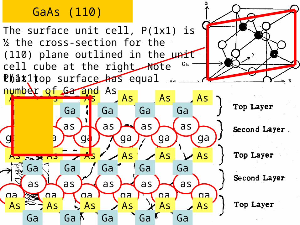
GaAs (110)
AsGa
AsGa
AsGa
AsGa
AsGa
As
AsGa
AsGa
AsGa
AsGa
AsGa
As
AsGa
AsGa
AsGa
AsGa
AsGa
As
P(1x1)
The surface unit cell, P(1x1) is ½ the cross-section for the (110) plane outlined in the unit cell cube at the right. Note that top surface has equal number of Ga and As
© copyright 2011 William A. Goddard III, all rights reservedCh120a-Goddard-L09 8
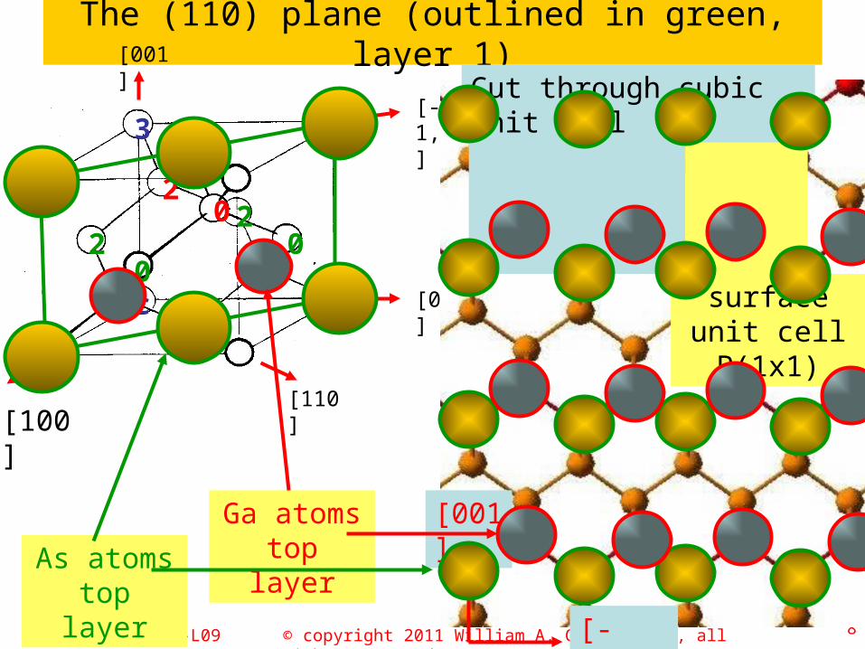
The (110) plane (outlined in green, layer 1)
As atoms top layer
1
1
c 1
3 1
02
1
2
1
0
11
20
[100]
[010]
[001]
[110]
[-1,1,0]
Ga atoms top layer
surface unit cell P(1x1)
[001]
[-1,1,0]
Cut through cubic unit cell
© copyright 2011 William A. Goddard III, all rights reservedCh120a-Goddard-L09 9
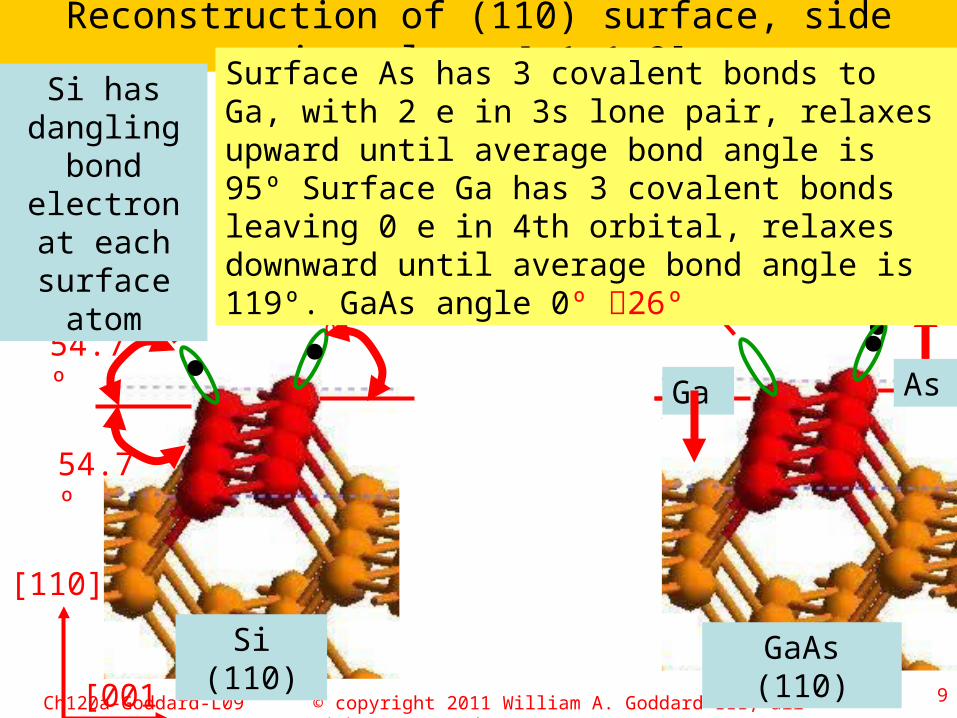
Reconstruction of (110) surface, side view along [-1,1,0]
[001]
[110]
54.7º54.7º
54.7º
Si (110)
Ga As
GaAs (110)
Si has dangling
bond electron at
each surface atom
Surface As has 3 covalent bonds to Ga, with 2 e in 3s lone pair, relaxes upward until average bond angle is 95º Surface Ga has 3 covalent bonds leaving 0 e in 4th orbital, relaxes downward until average bond angle is 119º. GaAs angle 0º 26º
© copyright 2011 William A. Goddard III, all rights reservedCh120a-Goddard-L09 10
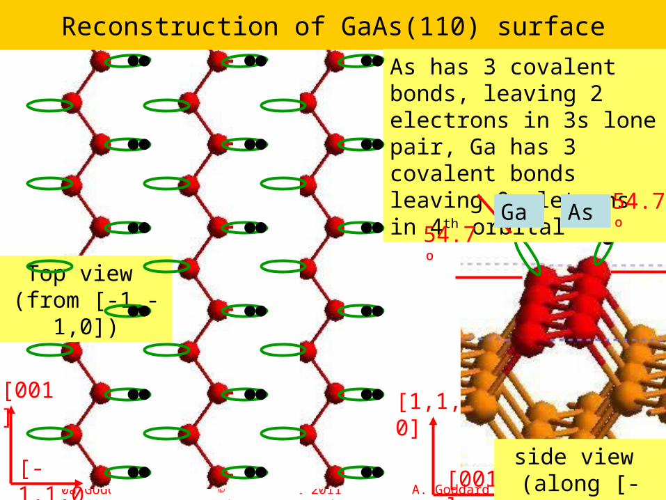
Reconstruction of GaAs(110) surface
Top view (from [-1,-1,0])
[001]
[-1,1,0] [001]
[1,1,0]
As has 3 covalent bonds, leaving 2 electrons in 3s lone pair, Ga has 3 covalent bonds leaving 0 eletrons in 4th orbital
54.7º54.7ºGa As
side view (along [-1,1,0])
© copyright 2011 William A. Goddard III, all rights reservedCh120a-Goddard-L09 11
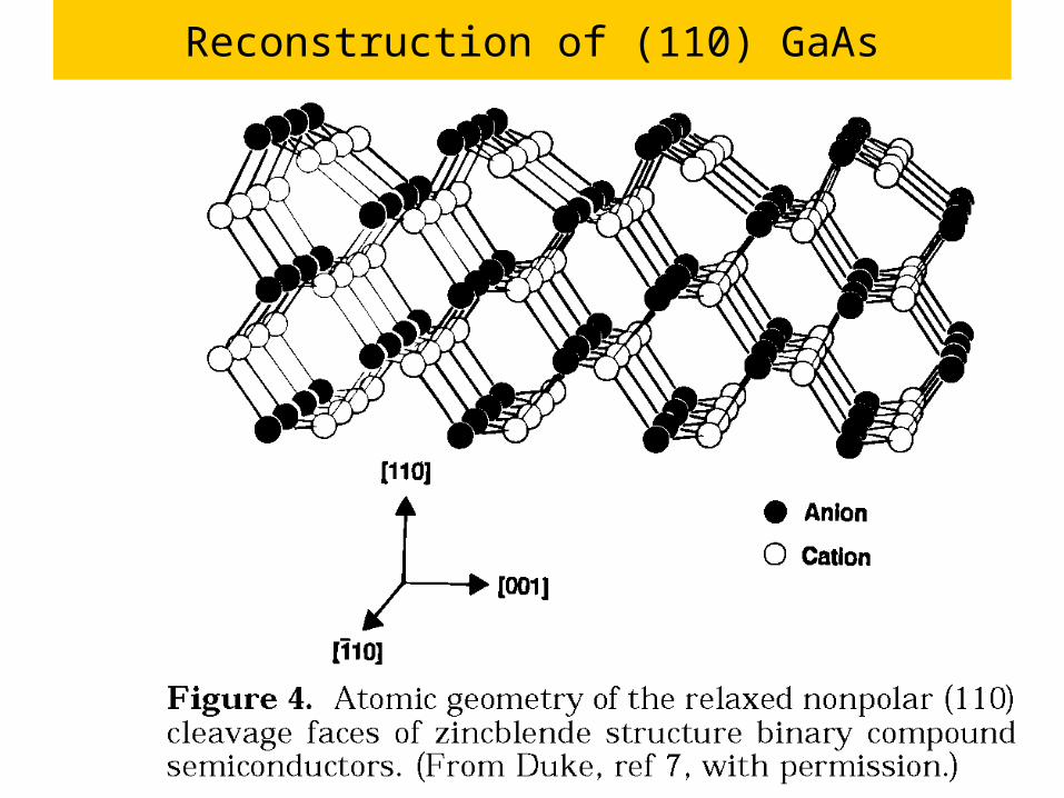
Reconstruction of (110) GaAs

© copyright 2011 William A. Goddard III, all rights reservedCh120a-Goddard-L09 12
III-V reconstruction dominated by local valence

© copyright 2011 William A. Goddard III, all rights reservedCh120a-Goddard-L09 13
© copyright 2011 William A. Goddard III, all rights reservedCh120a-Goddard-L09 16
Reconstruction of GaAs(110) surface, discussion
We consider that bulk GaAs has an average of 3 covalent bonds and one donor acceptor (DA) bond. But at the surface can only make 3 bonds so the weaker DA bond is the one broken to form the surface.
The result is that GaAs cleaves very easily compared to Si. No covalent bonds to break.
As has 3 covalent bonds, leaving 2 electrons in 3s lone pair. AsH3 has average bond angle of 92º. At the GaAs surface As relaxes upward until has average bond angle of 95º Ga has 3 covalent bonds leaving 0 eletrons in 4th orbital. GaH3 has average bond angle of 120º. At the GaAs surface Ga relaxes downward until has average bond angle of 119º.This changes the surface Ga-As bond from 0º (parallel to surface to 26º. Observed in LEED experiments and QM calculations
© copyright 2011 William A. Goddard III, all rights reservedCh120a-Goddard-L09 17
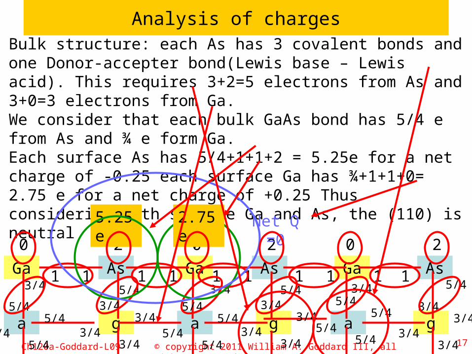
Analysis of chargesBulk structure: each As has 3 covalent bonds and one Donor-accepter bond(Lewis base – Lewis acid). This requires 3+2=5 electrons from As and 3+0=3 electrons from Ga.We consider that each bulk GaAs bond has 5/4 e from As and ¾ e form Ga. Each surface As has 5/4+1+1+2 = 5.25e for a net charge of -0.25 each surface Ga has ¾+1+1+0= 2.75 e for a net charge of +0.25 Thus considering both surface Ga and As, the (110) is neutral
As Ga As Ga AsGa
a g a ga g3/4
3/43/4
3/4
3/43/4
3/43/4
3/43/4
3/43/4
5/45/4
5/45/4
5/45/4
5/45/4
5/45/4
5/45/4
3/4 3/43/4 5/45/45/411 11 11 11 11
202020
5.25e 2.75e Net Q =0

© copyright 2011 William A. Goddard III, all rights reservedCh120a-Goddard-L09 18
GaAs (100)
ga ga
ga ga
ga ga
ga ga
ga ga
ga ga
ga
ga
ga
ga
ga
ga
Start with As at surface, denote Ga on 2nd layer as ga.
Then top layer is pure As. Not stable, get net negative charge at surface.
If cut off top layer, get pure Ga on surface
AsAs AsAs
AsAs AsAs
AsAs AsAs
AsAs AsAs
AsAs AsAs
AsAs AsAs
AsAs AsAs
© copyright 2011 William A. Goddard III, all rights reservedCh120a-Goddard-L09 19
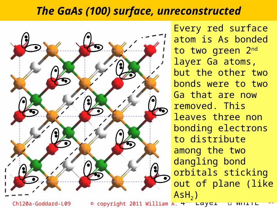
The GaAs (100) surface, unreconstructed
1st Layer RED2nd Layer GREEN3rd Layer ORANGE4th Layer WHITE
Every red surface atom is As bonded to two green 2nd layer Ga atoms, but the other two bonds were to two Ga that are now removed. This leaves three non bonding electrons to distribute among the two dangling bond orbitals sticking out of plane (like AsH2)
© copyright 2011 William A. Goddard III, all rights reservedCh120a-Goddard-L09 20
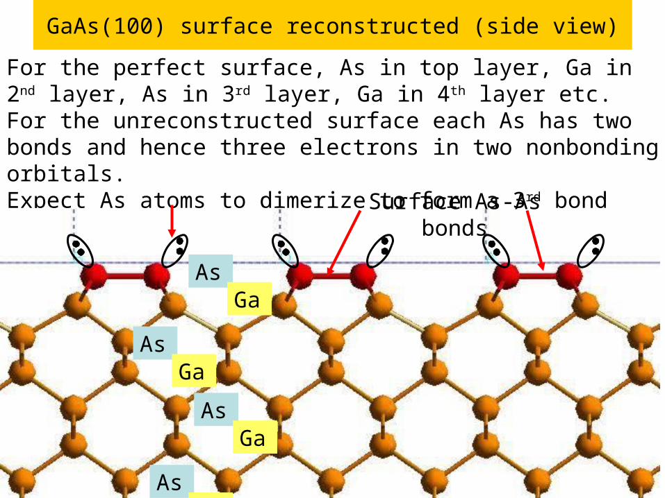
GaAs(100) surface reconstructed (side view)
For the perfect surface, As in top layer, Ga in 2nd layer, As in 3rd layer, Ga in 4th layer etc. For the unreconstructed surface each As has two bonds and hence three electrons in two nonbonding orbitals. Expect As atoms to dimerize to form a 3rd bond leaving 2 electrons in nonbonding orbitals. Surface As-As bonds
AsGa
AsGa
AsGa
AsGa

© copyright 2011 William A. Goddard III, all rights reservedCh120a-Goddard-L09 21
Charges for 2x1 GaAs(100)
2 2
2 21 1
1 1
3/4
3/4
3/4
3/4
5/4
5/4
5/43/4
3/4
3/4
3/4
3/4
3/4
3/4
3/4
3/4
3/4
3/4
3/4
5/4
5/4
5/4
Top layer, As
2nd layer, ga
3rd layer, as2e As-ga bond
2e As LP
2e As-As bond
2nd layer ga has 3 e
1st layer As has 5.5 e
Each surface As has extra 0.5 e dimer has extra 1e Not stable
© copyright 2011 William A. Goddard III, all rights reservedCh120a-Goddard-L09 22
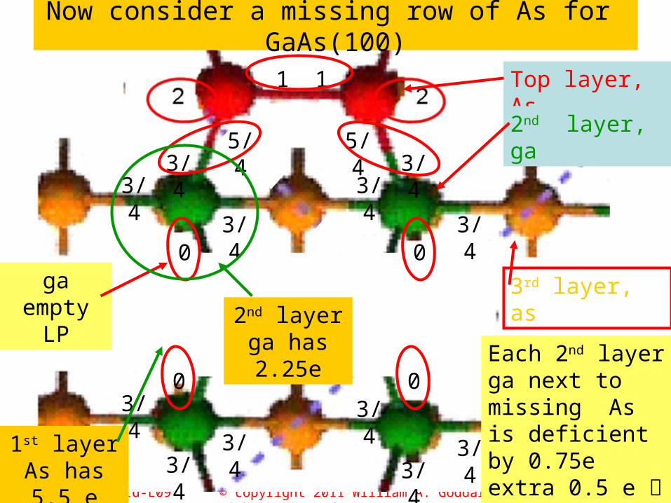
Now consider a missing row of As for GaAs(100)
1 1
3/43/4
3/4
5/4
3/4
3/4
3/43/4
3/4
3/4
3/43/4
3/4
5/4
Top layer, As
2nd layer, ga
3rd layer, asga empty LP
0
2nd layer ga has 2.25e
1st layer As has 5.5 e
Each 2nd layer ga next to missing As is deficient by 0.75e extra 0.5 e 4 ga are missing 3e
0
0 0

© copyright 2011 William A. Goddard III, all rights reservedCh120a-Goddard-L09 23
Consider 1 missing As row
out of 4Extra 1e
missing 3e
missing 3e
Extra 1e
Extra 1e
Extra 1e
-1-1-1+3=0 net charge
Thus based on electron counting expect simplest surface reconstruction to be 4x2. This is observed

© copyright 2011 William A. Goddard III, all rights reservedCh120a-Goddard-L09 24
Different views of GaAs(100)4x2 reconstruction
Previous page, 3 As dimer rows
then one missing
Two missing As row plus missing Ga rowExposes 3rd row As
Agrees with experimentHashizume et al Phys Rev B 51, 4200 (1995)
+1.5e-1.0e
© copyright 2011 William A. Goddard III, all rights reservedCh120a-Goddard-L09 25
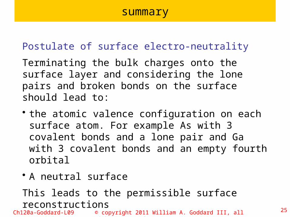
summary
Postulate of surface electro-neutrality
Terminating the bulk charges onto the surface layer and considering the lone pairs and broken bonds on the surface should lead to:• the atomic valence configuration on each surface atom.
For example As with 3 covalent bonds and a lone pair and Ga with 3 covalent bonds and an empty fourth orbital
• A neutral surface
This leads to the permissible surface reconstructions
© copyright 2011 William A. Goddard III, all rights reservedCh120a-Goddard-L09 26
As AsAsga gaga
As AsAsga gaga
As AsAsga gaga
As AsAsga gaga
As AsAsga gaga
As AsAsga gaga
As AsAsga gaga
As AsAsga gaga
As AsAsga gaga
As AsAsga gaga
ga
Asga
As
ga
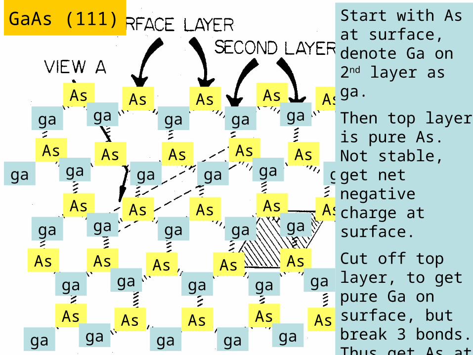
GaAs (111) Start with As at surface, denote Ga on 2nd layer as ga.
Then top layer is pure As. Not stable, get net negative charge at surface.
Cut off top layer, to get pure Ga on surface, but break 3 bonds. Thus get As at front always but back slab is Ga

© copyright 2010 William A. Goddard III, all rights reservedCh120a-Goddard-L09-10 27
Intrinsic semiconductors
+ -

© copyright 2010 William A. Goddard III, all rights reservedCh120a-Goddard-L09-10 28
Excitation energy
-4.0 eV relative to vacuum=-IP
-5.1 eV relative to vacuum = -EAEnergy gap = 1.1 eV

© copyright 2010 William A. Goddard III, all rights reservedCh120a-Goddard-L09-10 29
To be added – band states

© copyright 2010 William A. Goddard III, all rights reservedCh120a-Goddard-L09-10 30
To be added – band states
© copyright 2010 William A. Goddard III, all rights reservedCh120a-Goddard-L09-10 31
Semiconducting properties
© copyright 2010 William A. Goddard III, all rights reservedCh120a-Goddard-L09-10 32
Semiconducting properties
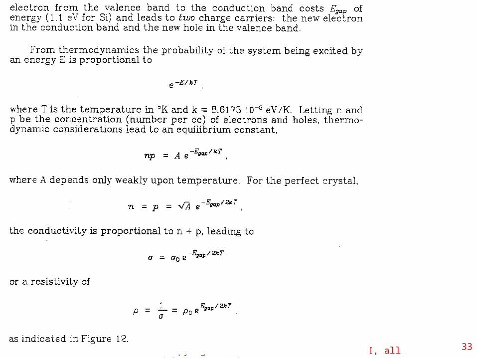
© copyright 2010 William A. Goddard III, all rights reservedCh120a-Goddard-L09-10 33

© copyright 2010 William A. Goddard III, all rights reservedCh120a-Goddard-L09-10 34
© copyright 2010 William A. Goddard III, all rights reservedCh120a-Goddard-L09-10 35

© copyright 2010 William A. Goddard III, all rights reservedCh120a-Goddard-L09-10 36
Trends: overlaps between bonded atoms decrease from 2p to 3p to 4p etcThus bonds are weaker, but antibonds are not as bandThus cohesive energy and band gaps decrease as go down the periodic table
© copyright 2010 William A. Goddard III, all rights reservedCh120a-Goddard-L09-10 37
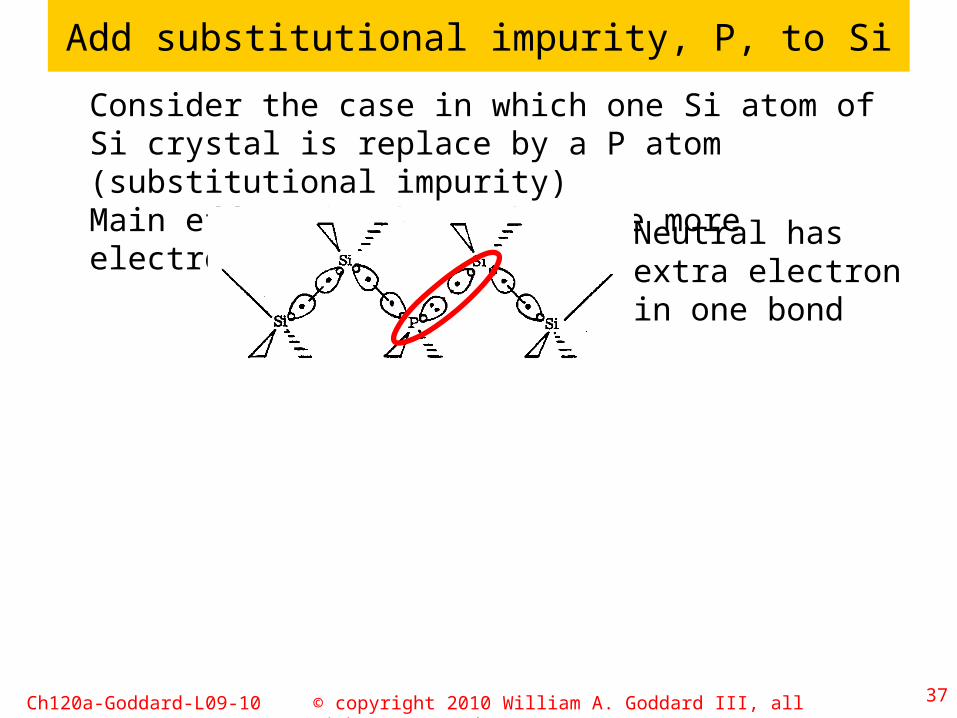
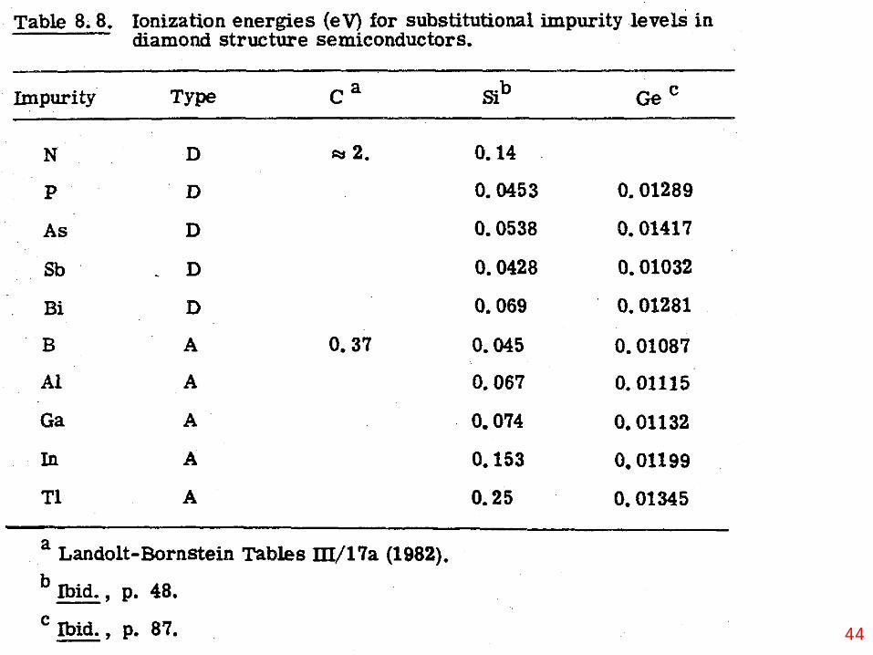
Add substitutional impurity, P, to Si
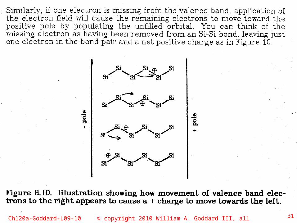
Consider the case in which one Si atom of Si crystal is replace by a P atom (substitutional impurity)Main effect is that P has one more electron than Si
Neutral has extra electron in one bond
© copyright 2010 William A. Goddard III, all rights reservedCh120a-Goddard-L09-10 38
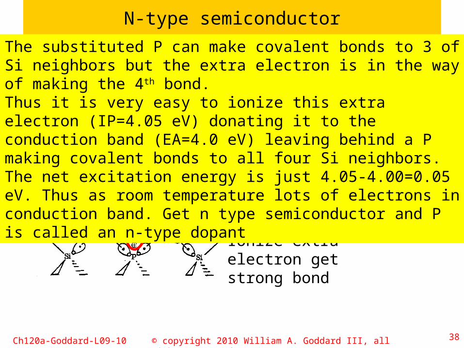
N-type semiconductor
Ionize extra electron get strong bond
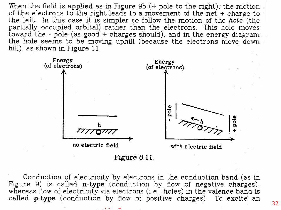
The substituted P can make covalent bonds to 3 of Si neighbors but the extra electron is in the way of making the 4th bond. Thus it is very easy to ionize this extra electron (IP=4.05 eV) donating it to the conduction band (EA=4.0 eV) leaving behind a P making covalent bonds to all four Si neighbors. The net excitation energy is just 4.05-4.00=0.05 eV. Thus as room temperature lots of electrons in conduction band. Get n type semiconductor and P is called an n-type dopant

© copyright 2010 William A. Goddard III, all rights reservedCh120a-Goddard-L09-10 39
To be added – band states
IP(P)=4.05 eV
Remove e from P, add to conduction band = 4.045-4.0 = 0.045 eV
Thus P leads to donor state just 0.045eV below LUMO or CBM
0.054 eV

© copyright 2010 William A. Goddard III, all rights reservedCh120a-Goddard-L09-10 40
Al substitutional impurity in Si
Consider the case in which one Si atom of Si crystal is replace by a Al atom (substitutional impurity)Main effect is that Al has one less electron than Si
The substituted Al can make covalent bonds to 3 of the Si neighbors but it lacks the electron to make a 4th bond 2-e bondThus the EA of add an electron to make the 2 electron bond is EA=5.033 eV, which is nearly as great as the IP=5.1 eV. Thus removing an electron from the valence band and adding it to the Al-Si bond costs only 5.1-5.033=0.067eV. leaving behind an Al making covalent bonds to all four Si neighbors.

© copyright 2010 William A. Goddard III, all rights reservedCh120a-Goddard-L09-10 41
Next consider Al substitutional impurity in Si
Since the net excitation energy 0.067 eV there are lots of holes in the valence band at room temperature. Get p type semiconductor and Al is called a p-type or acceptor dopant

© copyright 2010 William A. Goddard III, all rights reservedCh120a-Goddard-L09-10 42
To be added – band states
EA(Al)=5.033 eV
Add e to Al, from valence band = 5.1 -5.033 = 0.067 eV
Al leads to acceptor state just 0.067eV above HOMO or VBM
0.067 eV
© copyright 2010 William A. Goddard III, all rights reservedCh120a-Goddard-L09-10 43
© copyright 2010 William A. Goddard III, all rights reservedCh120a-Goddard-L09-10 44

© copyright 2010 William A. Goddard III, all rights reservedCh120a-Goddard-L09-10 45
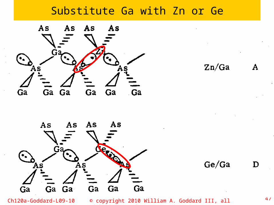
III-V Compounds
Energy Gaps for III-V much bigger than for group IV
Consider GaAs, what happens if we replace As with Se or GeWhat happens if we replace Ga with Zn or Ge

© copyright 2010 William A. Goddard III, all rights reservedCh120a-Goddard-L09-10 46
Substitute As for Se or Ge
© copyright 2010 William A. Goddard III, all rights reservedCh120a-Goddard-L09-10 47
Substitute Ga with Zn or Ge

© copyright 2010 William A. Goddard III, all rights reservedCh120a-Goddard-L09-10 48
Dopant levels for GaAs

© copyright 2010 William A. Goddard III, all rights reservedCh120a-Goddard-L09-10 49
Cohesive energies and Bonds for III-V compounds

© copyright 2010 William A. Goddard III, all rights reservedCh120a-Goddard-L09-10 50
Compare IV to III-V same row
© copyright 2010 William A. Goddard III, all rights reservedCh120a-Goddard-L09-10
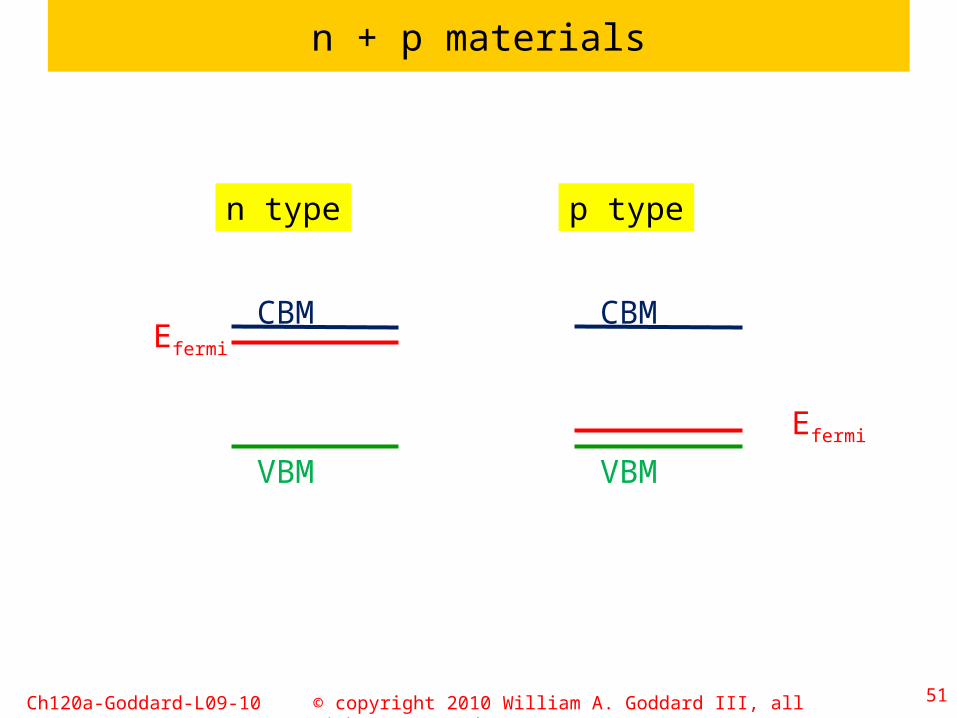
n + p materials
51
CBM
VBM
n type
Efermi
CBM
VBM
p type
Efermi

© copyright 2010 William A. Goddard III, all rights reservedCh120a-Goddard-L09-10
np junction
52
CBM
VBM
n type
Efermi
CBM
VBM
p type
Efermi
Get charge flow from n type to p type until Fermi energy (chemical potential) matches