naval postgraduate school - defense … board pcb layout.....61 f. translation board testing.....62...
TRANSCRIPT

NAVAL
POSTGRADUATE SCHOOL
MONTEREY, CALIFORNIA
THESIS
Approved for public release; distribution is unlimited
HARDWARE INTERFACE TO CONNECT AN AN/SPS–65 RADAR TO AN SRC–6E RECONFIGURABLE COMPUTER
by
Timothy L. King
March 2005
Thesis Advisor: Douglas J. Fouts Second Reader: Phillip E. Pace

THIS PAGE INTENTIONALLY LEFT BLANK
i
REPORT DOCUMENTATION PAGE Form Approved OMB No. 0704-0188 Public reporting burden for this collection of information is estimated to average 1 hour per response, including the time for reviewing instruction, searching existing data sources, gathering and maintaining the data needed, and completing and reviewing the collection of information. Send comments regarding this burden estimate or any other aspect of this collection of information, including suggestions for reducing this burden, to Washington headquarters Services, Directorate for Information Operations and Reports, 1215 Jefferson Davis Highway, Suite 1204, Arlington, VA 22202-4302, and to the Office of Management and Budget, Paperwork Reduction Project (0704-0188) Washington DC 20503. 1. AGENCY USE ONLY (Leave blank)
2. REPORT DATE March 2005
3. REPORT TYPE AND DATES COVERED Master’s Thesis
4. TITLE AND SUBTITLE: Hardware Interface to Connect an AN/SPS–65 Radar to an SRC–6E Reconfigurable Computer
6. AUTHOR(S) LT Timothy L. King
5. FUNDING NUMBERS
7. PERFORMING ORGANIZATION NAME(S) AND ADDRESS(ES) Naval Postgraduate School Monterey, CA 93943-5000
8. PERFORMING ORGANIZATION REPORT NUMBER
9. SPONSORING /MONITORING AGENCY NAME(S) AND ADDRESS(ES) NSA 9800 Savage Road Ft. George C. Meade, MD 20755
10. SPONSORING/MONITORING AGENCY REPORT NUMBER
11. SUPPLEMENTARY NOTES The views expressed in this thesis are those of the author and do not reflect the official policy or position of the Department of Defense or the U.S. Government. 12a. DISTRIBUTION / AVAILABILITY STATEMENT Approved for public release; distribution is unlimited
12b. DISTRIBUTION CODE
13. ABSTRACT (maximum 200 words) A hardware interface is designed, developed, constructed, and tested to interface a naval radar to the SRC–6E re-configurable computer. The U.S. Navy AN/SPS–65 radar provides in-phase (I) and quadrature (Q) channels along with the AGC voltage to the hardware interface in analog form. The hardware interface receives a sampling clock from the SRC–6E and in turn performs the requisite attenuation and digital conversion before presenting the sig-nals to the SRC–6E through its CHAIN port. The results show that the SRC–6E can effectively generate a sam-pling clock to drive the analog-to-digital converters and that real-time radar data can be brought into the SRC–6E via its high speed CHAIN port for performing high speed digital signal processing
15. NUMBER OF PAGES
127
14. SUBJECT TERMS Radar Signal Processing, Reconfigurable Computer, SRC-6E, SRC
16. PRICE CODE
17. SECURITY CLASSIFICATION OF REPORT
Unclassified
18. SECURITY CLASSIFICATION OF THIS PAGE
Unclassified
19. SECURITY CLASSIFICATION OF ABSTRACT
Unclassified
20. LIMITATION OF ABSTRACT
UL NSN 7540-01-280-5500 Standard Form 298 (Rev. 2-89) Prescribed by ANSI Std. 239-18

ii
THIS PAGE INTENTIONALLY LEFT BLANK

iii
Approved for public release; distribution is unlimited
HARDWARE INTERFACE TO CONNECT AN AN/SPS–65 RADAR TO AN SRC–6E RECONFIGURABLE COMPUTER
Timothy L. King
Lieutenant, United States Naval Reserve B.S., Virginia Polytechnic & State University, 2000
Submitted in partial fulfillment of the requirements for the degree of
MASTER OF SCIENCE IN ELECTRICAL ENGINEERING
from the
NAVAL POSTGRADUATE SCHOOL March 2005
Author: Timothy L. King
Approved by: Douglas J. Fouts
Thesis Advisor
Phillip E. Pace Second Reader
John P. Powers Chairman, Department of Electrical and Computer Engineering

iv
THIS PAGE INTENTIONALLY LEFT BLANK

v
ABSTRACT
A hardware interface is designed, developed, constructed, and tested to interface a
naval radar to the SRC–6E reconfigurable computer. The U.S. Navy AN/SPS–65 radar
provides in-phase (I) and quadrature (Q) channels along with the AGC voltage to the
hardware interface in analog form. The hardware interface receives a sampling clock
from the SRC–6E and in turn performs the requisite attenuation and digital conversion
before presenting the signals to the SRC–6E through its CHAIN port. The results show
that the SRC–6E can effectively generate a sampling clock to drive the analog-to-digital
converters and that real- time radar data can be brought into the SRC–6E via its high
speed CHAIN port for performing high speed digital signal processing.

vi
THIS PAGE INTENTIONALLY LEFT BLANK

vii
TABLE OF CONTENTS
I. INTRODUCTION .......................................................................................................1 A. PURPOSE.........................................................................................................1 B. DESIGN OVERVIEW ....................................................................................1 C. THESIS OUTLINE .........................................................................................3
II. SRC–6E ARCHITECTURE.......................................................................................5 A. INTRODUCTION ...........................................................................................5 B. SRC–6E SYSTEM ARCHITECTURE OVERVIEW..................................5 C. CHAIN PORT OVERVIEW ..........................................................................7
1. CHAIN Port Physical Configuration .................................................7 2. Implementation as a General Purpose Port ......................................8
D. DESIGN IMPLEMENTATION.....................................................................9 E. CHAPTER SUMMARY .................................................................................9
III. AN/SPS–65..................................................................................................................11 A. INTRODUCTION .........................................................................................11 B. RADAR SELECTION...................................................................................11 C. AN/SPS–65(V)1 OPERATIONAL OVERVIEW........................................11 D. DESIGN IMPLEMENTATION...................................................................13 E. CHAPTER SUMMARY ...............................................................................15
IV. MAXIM MAX108EVKIT 8-BIT ADC BOARD.....................................................17 A. INTRODUCTION .........................................................................................17 B. OVERALL CAPABILITIES OF THE MAX108 .......................................17 C. POWER REQUIREMENTS ........................................................................19 D. ANALOG AND CLOCK INPUTS ...............................................................21
1. Sample Clock Inputs..........................................................................21 2. Analog Inputs .....................................................................................21
E. DIGITAL OUTPUTS ....................................................................................21 1. Demultiplexer Operation ..................................................................23
a. Non–Demultiplexed Mode ......................................................24 b. Demultiplexed Mode ...............................................................24 c. Decimation Mode ....................................................................25
2. Data Ready .........................................................................................26 F. DESIGN IMPLEMENTATION...................................................................27
1. Input Configuration...........................................................................27 2. Sample Clock and Demux Operation ..............................................27 3. Data Ready .........................................................................................28 4. Termination and Power Supplies.....................................................28
G. INITIAL TESTING AND FAMILIARIZATION ......................................29 H. ADDITIONAL HARDWARE REQUIRED................................................30 I. CHAPTER SUMMARY ...............................................................................31

viii
V. ANALOG PCB DESIGN ..........................................................................................33 A. INTRODUCTION .........................................................................................33 B. ATTENUATION DESIGN OPTIONS ........................................................33
1. Inline RF Attenuator and Buffer......................................................33 2. Op–Amp Attenuation Circuit ...........................................................34 3. Voltage Divider to High–Speed Buffer............................................35
C. PRF TIMING REFERENCE AMPLIFICATION DESIGN.....................37 D. PCB DESIGN AND LAYOUT .....................................................................40
1. PCB Software Selection.....................................................................40 2. Analog Board Schematic Layout......................................................40 3. Analog Board PCB Design................................................................43
E. TESTING........................................................................................................45 1. I and Q Channel Testing ...................................................................46 2. AGC Voltage Testing .........................................................................48 3. PRF Timing Reference Testing ........................................................49
F. CHAPTER SUMMARY ...............................................................................50
VI. TRANSLATION BOARD DESIGN ........................................................................51 A. INTRODUCTION .........................................................................................51 B. SIGNAL TRANSLATION............................................................................51
1. LVPECL–to–LVTTL Translation...................................................51 2. LVTTL–to–ECL Translation...........................................................52
C. MICTOR CONNECTOR ALTERNATIVES .............................................52 1. Custom Micro–Coaxial Cable ..........................................................53 2. MICTOR Connector Breakout Adapter.........................................53 3. Printed Circuit Board Implementation...........................................53
D. MAX108EVKIT–TO–TRANSLATION BOARD CABLING...................54 E. PCB DESIGN AND LAYOUT .....................................................................55
1. Initial Design Considerations ............................................................55 2. Device Termination ...........................................................................56 3. Power Distribution.............................................................................58 4. Translation Board Schematic Layout ..............................................59 5. Translation Board PCB Layout .......................................................61
F. TRANSLATION BOARD TESTING..........................................................62 1. Sample Clock Translation Testing ...................................................64 2. LVPECL–to–LVTTL Translation Testing ......................................65 3. LVPECL Termination Resistor Analysis ........................................67
G. CHAPTER SUMMARY ...............................................................................68
VII. COMPLETE INTERFACE TESTING ...................................................................71 A. INTRODUCTION .........................................................................................71 B. DESIGN MODIFICATION..........................................................................71 C. INTERFACE TEST.......................................................................................71 D. CHAPTER SUMMARY ...............................................................................73
VIII. CONCLUSIONS........................................................................................................75 A. DESIGN SUMMARY....................................................................................75

ix
B. DESIGN ACCOMPLISHMENT .................................................................76 C. RECOMMENDATIONS FOR FUTURE WORK .....................................77
APPENDIX A CHAIN PORT PIN LISTING (AFTER REFS. 6 & 7.)..................79
APPENDIX B SRC–6E PART NUMBERS..............................................................83 A. USER LOGIC FPGAS [6].............................................................................83 B. MICRO–COAXIAL CABLE [6] ..................................................................83 C. 114–PIN AMP MICTOR CONNECTOR [6] ..............................................83
APPENDIX C LOGIC ANALYZER DATA............................................................85
APPENDIX D MATLAB LOGIC ANALYZER PLOTTING SCRIPT ................93
APPENDIX E SPICE MODEL OF ATTENUATION CIRCUIT..........................95
APPENDIX F SPICE MODEL OF PRF TIMING REFERENCE AMPLIFIER 97
APPENDIX G EXPRESSPCB MANUFACTURING SPECIFICATIONS...........99
APPENDIX H MICTOR CONNECTOR SCHEMATIC......................................101
LIST OF REFERENCES ....................................................................................................103
INITIAL DISTRIBUTION LIST.......................................................................................107

x
THIS PAGE INTENTIONALLY LEFT BLANK

xi
LIST OF FIGURES Figure 1. AN/SPS–65 to SRC–6E Hardware Interface Block Diagram...........................2 Figure 2. SRC–6E System Architecture Block Diagram (From Ref. 5.) ..........................6 Figure 3. MAP Chassis Configuration (After Ref. 5.) ......................................................7 Figure 4. AN/SPS–65 Receiver Block Diagram (After Ref. 8.) .....................................13 Figure 5. AN/SPS–65 Block Diagram Illustrating Test Point Taps (After Ref. 8.)........14 Figure 6. MAXIM MAX108EVKIT...............................................................................18 Figure 7. MAX108EVKIT Power Supply Connections .................................................20 Figure 8. MAX108EVKIT Digital Output Termination (From Ref. 10.) .......................23 Figure 9. Non-Demuxed, DIV1 Timing Diagram (From Ref. 9.)...................................24 Figure 10. Demuxed, DIV2 Timing Diagram (From Ref. 9.) ...........................................25 Figure 11. Decimation, DIV4 Mode Timing Diagram (From Ref. 9.) .............................26 Figure 12. CLK and DREADY Timing in DIV2 mode Showing the Two Possible
Phases of DREADY (From Ref. 9.) ................................................................27 Figure 13. Reconstructed Output from MAX108EVKIT Testing ....................................30 Figure 14. Two–Resistor Voltage Divider and Buffer Circuit..........................................35 Figure 15. AC Sweep Analysis of the LMH6559 .............................................................37 Figure 16. PRF Timing Reference LVTTL Amplification Circuit ...................................38 Figure 17. Simulation of PRF Timing Reference Amplifier Circuit ................................39 Figure 18. Complete Analog Board Schematic .................................................................42 Figure 19. PCB CAD Drawing for Analog Board ............................................................45 Figure 20. Assembled Analog Board ................................................................................46 Figure 21. Test of I Channel Attenuation Circuit .............................................................47 Figure 22. Test of Q Channel Attenuation Circuit ............................................................48 Figure 23. Test of AGC Voltage Attenuation Circuit .......................................................49 Figure 24. Test of PRF Timing Reference Amplification Circuit ....................................50 Figure 25. Shielded Controlled Impedance Cable ............................................................55 Figure 26. Block Diagram of Translation Board and MAX108EVKIT Arrangement .....56 Figure 27. Translation Board Schematic...........................................................................60 Figure 28. PCB CAD Drawing of Translation Board .......................................................62 Figure 29. Translation Board Trace Errors .......................................................................63 Figure 30. Assembled Translation Board..........................................................................63 Figure 31. 10–MHz LVTTL Clock Translated to ECL ....................................................64 Figure 32. 200–MHz LVTTL Clock Translated to ECL ..................................................65 Figure 33. Translation Board Output with a 200–MHz Sample Clock.............................66 Figure 34. DREADY Immediately Following Translation (Terminator Located on
MAX108EVKIT).............................................................................................68 Figure 35. DREADY Immeditely Following Translation (Terminator Located on
Translation Board) ...........................................................................................68 Figure 36. Complete Hardware Interface Configuration ..................................................72 Figure 37. Reconstructed Radar Data Collected by the SRC–6E (From Ref. 23.) ...........73

xii
THIS PAGE INTENTIONALLY LEFT BLANK

xiii
LIST OF TABLES Table 1. SRC–6E CHAIN Port Signal Groupings (From Ref. 6.) ...................................8 Table 2. AN/SPS–65 Channel Parameters.....................................................................14 Table 3. Power Supply Requirements [9] ......................................................................20 Table 4. Ideal Input Voltage and Output Code Results for Single–ended Operation
(From Ref. 10.) ................................................................................................22 Table 5. Ideal Input Voltage and Output Code Results for Single–ended Operation
(From Ref. 10.) ................................................................................................22 Table 6. MAX108EVKIT Demultiplexer Jumper Settings [10]....................................24 Table 7. Resistor Values for Voltage Divider................................................................35 Table 8. Trace Impedance Calculation Results .............................................................43 Table 9. Resistor Size and Power Handling Comparison..............................................44 Table 10. Shielded Controlled Impedance Cable Electrical Properties (From Ref.
20.) ...................................................................................................................55 Table 11. Termination Resistor Power Calculations .......................................................58 Table 12. Translation Board Voltage and Current Requirements ...................................58 Table 13. Trace Width Current Capacity (From Ref. 22.)...............................................62

xiv
THIS PAGE INTENTIONALLY LEFT BLANK

xv
ACKNOWLEDGMENTS I would like to thank my thesis advisor Douglas J. Fouts for his time, support and techni-
cal guidance. His involvement was essential in ensuring that this project stayed on track
and succeeded not only in function, but also in providing a great learning experience that
covered multiple electrical engineering disciplines.
A special thanks to David Rigmaiden for his printed circuit board expertise and soldering
skills. His assistance was instrumental in the successful mounting of the MICTOR con-
nector on the translation board and the implementation of corrective measures to work
around design errors in both the ana log and translation printed circuit boards.
SRC Computers, Inc. needs to be recognized for their design guidance and provisioning
of specialized hardware. Without the micro-coaxial cables and breakout board they pro-
vided, the implementation and testing of the hardware interface would not have been pos-
sible in the time allotted for the project.
I would also like to Alan Hunsberger and the National Security Agency for providing me
the opportunity to conduct this research.
Most importantly, I thank my wife Alice for being my strongest supporter. Over the past
27 months here at the Naval Postgraduate School she filled the role as sounding board,
proofreader, and at times educator while simultaneously acting as wife, mother, and
friend.

xvi
THIS PAGE INTENTIONALLY LEFT BLANK

xvii
EXECUTIVE SUMMARY
Reconfigurable computers provide the military a highly customizable and power-
ful way to process real–time data. The purpose of this research was to test the capability,
exploit the functionality, and prove the feasibility of the SRC–6E reconfigurable com-
puter to send and receive data via its high speed CHAIN port. The use of FPGAs on the
reconfigurable MAP® boards of the SRC–6E provides the SRC–6E the ability to generate
algorithm specific logic, with the potential for orders of magnitude speedup for computa-
tionally intensive algorithms [1]. Studies have been conducted proving that speedup can
be obtained by reconfigurable computers but they have only addressed non-real-time
computational intensive problems in which the data being analyzed is already stored on
the machine. By bringing data straight to the reconfigurable computer, its parallel proc-
essing capabilities can be used to perform real–time data processing.
Reconfigurable computers offer high performance because they can be custom-
ized to the problem and they are relatively fast due to highly parallel and spatial execu-
tion [2]. Adding the ability to process large amounts of data in real-time gives recon-
figurable computing the potential to evolve into efficient signal processors. Instead of
having specialized gear for cryptographic analysis, radar processing, or electronic signal
collection, a single SRC–6E, through its CHAIN port, can capture the requisite data and
process it through hardware. This capability is very attractive in light of the ever increas-
ing cost and complexity of signal processing equipment. Therefore, it was essential that
this research use a valid real–world example to test the CHAIN port of the SRC–6E and
determine its capabilities and limitations.
To prove the real–world applicability of such an interface, the AN/SPS–65 radar
was selected as the data source. The goal of the hardware interface design was then to
develop, implement, and test the requisite hardware needed to permit the SRC–6E to
process the data received by the AN/SPS–65 to calculate the range of a target.
The data received by the AN/SPS–65 is carried on the ± 5.8 V in–phase (I) and
quadrature (Q) channels while the internal amplification value of these two channels is

xviii
carried on the separate 0–12 V automatic gain control (AGC) voltage signal. The
AN/SPS–65 pulse repetition frequency (PRF) is synchronized to 0 to 1.0–V pulse that
generates a timing reference for the received radio frequency (RF) signals. The signals
were connected to a custom–built analog board which buffered each signal and either
amplified or attenuated the signal for proper compatibility with other parts of the design.
The I, Q, and AGC voltage signals were attenuated to ± 225 mV to be compatible with
the MAX108 ADC analog inputs and the PRF timing reference signal was amplified to
low–voltage transistor–transistor–logic (LVTTL) to be compatible with the SRC–6E.
The I, Q, and AGC voltage signals were connected to individual MAX108 evalua-
tion kits (MAX108EVKIT) where they were sampled at 100 MHz by the MAX108
ADCs. The low–voltage positive emitter coupled logic (LVPECL) outputs of each
MAX108EVKIT were routed via shielded controlled impedance cables to a custom–built
translation board. On the translation board, the LVPECL signals were translated to
LVTTL and routed, along with the PRF timing reference signal from the analog board, to
a 114–pin MICTOR™ connector. Micro–coaxial cable was then used to connect the
MICTOR connector of the translation board to the MICTOR connector of the CHAIN
port on the SRC–6E, completing the interface between the radar and the SRC–6E. The
translation board also took the 100–MHz sample clock generated by the SRC–6E from
the MICTOR connector and translated it into a differential emitter coupled logic (ECL)
clock. This differential ECL clock was then routed through a clock driver for distribution
to the three MAX108EVKITs.
The design met the established goal of interfacing the AN/SPS–65 radar to the
SRC–6E reconfigurable computer. The design tested focused only on the single data rate
(SDR) mode of the SRC–6E, but engineered all aspects of the design to be capable of ex-
ploiting the double data rate (DDR) capability of the SRC–6E allowing room for future
speed–ups. To provide flexibility of implementation, the bandwidth of the analog board
and the MAX108EVKITs allow the design to be capable of interfacing with other radars
with similar output signals as the AN/SPS–65. Ultimately, the designed proved that the
CHAIN port of the SRC–6E is a very capable high–speed port that can be effectively in-
terfaced with external devices through user–defined hardware.

1
I. INTRODUCTION
A. PURPOSE
Reconfigurable computers provide the military a highly customizable and power-
ful way to process real–time data. The purpose of this research was to test the capability,
exploit the functionality, and prove the feasibility of the ability of the SRC–6E recon-
figurable computer to send and receive data via its high speed CHAIN port. The use of
FPGAs on the reconfigurable MAP® boards of the SRC–6E provides the SRC–6E the
ability to generate algorithm specific logic, with the potential for orders of magnitude
speedup for computationally intensive algorithms [1]. Studies have been conducted prov-
ing that speedup can be obtained by reconfigurable computers, but they have only ad-
dressed non-real-time computational intensive problems in which the data being analyzed
is already stored on the machine. By bringing data straight to the reconfigurable com-
puter, its parallel processing capabilities can be used to perform real-time data process-
ing.
Reconfigurable computers offer high performance because they can be custom-
ized to the problem and they are relatively fast due to their highly parallel and spatial
execution [2]. Adding the ability to process large amounts of data in real-time gives re-
configurable computing the potential to evolve into efficient signal processors. Instead of
having specialized gear for cryptographic analysis, radar processing, or electronic signal
collection, a single SRC–6E, through its CHAIN port, can capture the requisite data and
process it through hardware. This capability is very attractive in light of the ever increas-
ing cost and complexity of signal processing equipment. Therefore, it was essential that
this research use a valid real–world example to test the CHAIN port of the SRC–6E and
determine its capabilities and limitations.
B. DESIGN OVERVIEW
The design illustrated in Figure 1 began by selecting a suitable real–world device
that would produce real–time data to be processed by the SRC–6E. The U.S. Navy
AN/SPS–65 search radar used by the Electrical Engineering Department at the Naval

2
Postgraduate School was selected to fulfill this role. The AN/SPS–65 provided access to
its in–phase (I) channel, quadrature (Q) channel, and automatic gain control (AGC) volt-
age, as well as its pulse repetition frequency (PRF) timing reference signal which could
be used to perform basic radar signal processing. Located on the tallest academic build-
ing on campus, the Naval Postgraduate School AN/SPS–65 could track a wide array of
real targets, ranging from ships in Monterey Bay, the Santa Cruz Mountains, and aircraft
on approach to the Monterey Airport. The real–world nature of the radar signals and the
ease of access to them made the AN/SPS–65 a convenient and effective signal source for
the project.
Figure 1. AN/SPS–65 to SRC–6E Hardware Interface Block Diagram
An analog board was designed and implemented to attenuate and buffer the I, Q,
and AGC voltage signals from the AN/SPS–65 to a range of ± 250 mV for connection to
the analog–to–digital converters. This analog board also amplified the pulse repetition
frequency signal from a non-standard range of 0 to + 1.1 V to the low–voltage transistor–
transistor–logic (LVTTL) range of 0 to + 3.3 V for direct connection to the SRC–6E.
Three MAX108 evaluation kits (MAX108EVKIT), each providing 8–bits of reso-
lution, were then implemented to perform the analog–to–digital conversion (ADC) of the
radar signals prepped by the analog board. Each MAX108EVKIT was to receive a 200–
MHz sample clock generated by the SRC–6E. Each MAX108EVKIT would then demul-
tiplex the output data to reduce the data rate into the SRC–6E to 100 MHz. This would
create two sets of 8–bit data per MAX108EVKIT in differential low–voltage positive
Data Lines
200 MHz Clock
SRC–6E
MAX108EVs MAX9360
LVTTL to ECL
MAX9316A
Clock Driver
MC100EPT23
LVPECL to
LVTTL
Data Ready
TRANSLATION BOARD
Voltage Divider &
Buffer Circuit
ADC
ADC
ADC
LVTTL Amplifier
AN/SPS -65
Analog I
Analog Q
AGC
PRF
ANALOG BOARD
I
Q
AGC

3
emitter–coupled logic (LVPECL) format. Prior to connecting to the SRC–6E, these
LVPECL outputs needed to be converted to the LVTTL logic standard of the SRC–6E.
To complete the interface, a translation board was designed and implemented to
first translate the digitized radar signals from LVPECL to LVTTL. The board then con-
nected the translated signals and the amplified pulse repetition frequency to the SRC–6E
cabling through a surface mounted MICTOR™ connector. Finally, the translation board
provided the necessary conversion of the LVTTL sample clock generated by the SRC–6E
so that it could drive the emitter–coupled logic (ECL) clocks of the MAX108EVKITs.
C. THESIS OUTLINE
Each of the following chapters represents a major design area that needed to be
addressed throughout the entire design process. The list below gives a brief synopsis of
the remaining chapters:
• Chapter II describes the SRC–6E architecture, the CHAIN port interface, and external hardware requirements.
• Chapter III discusses the reasons for selecting the AN/SPS–65 radar, its basic operation, and how it was implemented in the design.
• Chapter IV discusses the selection, features, and design implementation of the MAX108 ADCs for the design.
• Chapter V covers the design, implementation, and testing of an ana log printed circuit board designed to attenuate the three signals from the AN/SPS–65 to a level suitable for sampling by the MAX108s while also amplifying the pulse repetition frequency of the radar to LVTTL levels.
• Chapter VI covers the design, implementation, and testing of the printed circuit board responsible for providing the hardware interface between the SRC–6E and the MAX108 ADCs.
• Chapter VII discusses the complete interface testing and the overall re-sults.
• Chapter VIII discusses the design conclusions and potential follow on work.

4
THIS PAGE INTENTIONALLY LEFT BLANK

5
II. SRC–6E ARCHITECTURE
A. INTRODUCTION
Reconfigurable computers could one day augment and possibly replace bulky and
expensive specialized digital signal processing equipment. Studies have already proven
that FPGA implementations are one to two orders of magnitude faster than typical em-
bedded processors [3]. To harness this parallel processing power, reconfigurable com-
puters must be successfully interfaced with already proven high–speed data sources. This
design focused on interfacing the SRC–6E reconfigurable computer to an AN/SPS–65
radar using the high–speed CHAIN port of the SRC–6E. This chapter provides a brief
system overview of the SRC–6E and describes the physical architecture and implementa-
tion of its high–speed CHAIN port.
B. SRC–6E SYSTEM ARCHITECTURE OVERVIEW
The SRC–6E is comprised of two microprocessor chassis and a reconfigurable
MAP® chassis. Each microprocessor chassis consists of dual 1–GHz Intel® Pentium® III
XeonTM processors running the Linux operating system, 1.5 gigabytes of RAM, and a
SNAP® port. The SNAP port connects the microprocessor chassis to one of the recon-
figurable MAPs on the MAP chassis. Code is compiled and run on the Xeon processors,
placing specialized functions on the MAP. These specialized functions are usually com-
putationally intensive and can exploit the speedups afforded by hardware execution. Fig-
ure 2 illustrates the basic block diagram of the SRC–6E system configuration. [4]

6
Figure 2. SRC–6E System Architecture Block Diagram (From Ref. 5.)
The MAP chassis contains two reconfigurable MAPs, each consisting of two Xil-
inx® Virtex®–II FPGAs, a control processor, a total of 24 Mbytes of dual ported RAM,
one SNAP port, and two CHAIN® ports. The two CHAIN ports (CHAIN In and CHAIN
Out) are data ports that can be configured to connect the two MAPs together or be used
as general input and output ports [6]. Figure 3 shows the actual layout of the MAP chas-
sis. Most of the features inherent to the Virtex–II are available to the SRC–6E program-
mer, with a few exceptions. The two most notable are the FPGA clock frequency and the
input and output levels. Though the Virtex–II FPGAs are capable of operating with a
420–MHz system clock [7], the MAPs on the SRC–6E restricts the system bus speed to
100 MHz. In addition, the internal voltage settings on the MAP set the input and output
logic levels of the FPGAs to LVTTL.

7
Figure 3. MAP Chassis Configuration (After Ref. 5.)
C. CHAIN PORT OVERVIEW
The CHAIN port is the dual–purpose high–speed parallel data port that allows ei-
ther the interconnection of user logic between MAPs or the connection of user defined
hardware to the SRC–6E. The CHAIN port supports user–defined data rates up to a
maximum rate of 100 MHz in both single data rate (SDR) and double data rate (DDR)
configurations. When in the SDR configuration, the CHAIN port can transfer data at
9,600 MBps. The data rate doubles to 19,200 MBps when the CHAIN port is used in the
DDR configuration. The data flow onto the MAP through the CHAIN port must be
source synchronous with a clock signal traveling with the data to indicate to the user
logic when to latch the data. [6]
1. CHAIN Port Physical Configuration
Each CHAIN port has a total of 104 bi–directional signal lines that connect di-
rectly to the user logic FPGA input and output pins. The physical layout of the MAP
separates these signals into four groups as listed in Table 1. The user is free to modify
the groupings and functions of these bits as long as source synchronous data flow is
maintained. Since the signals connect directly to the Virtex–II FPGAs, the user can de-
fine any signal to match its corresponding Virtex–II pin setting [6]. However, SRC took

8
extreme care to place the clock bits listed in Table 1 on the GCLKx input and output pins
of the Virtex-II FPGAs. These pins are specifically designed and optimized to distribute
clock signals on and off the FPGA, but can be used for general input and output when not
used for clock distribution purposes [7]. Appendix A lists the CHAIN port pin numbers,
the corresponding Vir tex–II pin numbers, and the Virtex–II pin descriptions.
Table 1. SRC–6E CHAIN Port Signal Groupings (From Ref. 6.)
Port Signal Group A Port Signal Group B Port Signal Group C Port Signal Group D
36 Data Bits 36 Data Bits 20 Data Bits 6 Data Bits (SDR only)
1 Data Valid Bit 1 Data Valid Bit
1 Clock Bit 1 Clock Bit
1 Full Bit 1 Full Bit
2. Implementation as a General Purpose Port
Since the user logic determines the function of the CHAIN port signals, the sig-
nals can be redefined to suit the particular needs of the user. When redefining the signals,
the user must take care to ensure the correct Virtex–II input/output buffers are selected
and that the signal levels are driven at LVTTL. Working within the confines of these two
requirements, the user can fully customize the CHAIN port to interface with external
hardware. [6]
The SRC–6E uses 114–pin AMP™ MICTOR surface mount connectors for all
the SNAP and CHAIN port connections on the MAP board. A custom 50 −Ω micro–
coaxial cable with 114–pin push–in AMP connectors is then used to provide the neces-
sary cabling between the surface mount connectors. SRC Computers highly recommends
using the same micro–coaxial cables and surface mount MICTOR connector when con-
necting external hardware to the SRC–6E. This enables compatible high–speed connec-
tions between the user hardware and the MAP board. Appendix B lists the specific part
numbers and manufacturer data of the parts required to establish a connection to the
CHAIN port. [6]
To ensure proper signal transmission between the user hardware and the SRC–6E,
the user hardware must pay particular attention to the trace impedance and signal termi-
nation. All transmission lines on the user hardware should be impedance matched as

9
closely as possible to the impedance of the micro–coaxial cable. Since the FPGAs have
no termination resistors and the CHAIN port signals connect directly to the FPGA, the
user hardware must handle all signal termination. For signals being transmitted to the
SRC–6E, SRC Computers recommends implementing a source–series resistive termina-
tion on the data line. The resistive termination value, when summed with the driver out-
put impedance, should match the 50 −Ω impedance of the micro–coaxial cable as close
as possible. For signals being transmitted by the SRC–6E, an RC shunt type termination
should be implemented using a 50 −Ω resistor in series with a 0.01 µF− capacitor. [6]
D. DESIGN IMPLEMENTATION
The design required that the CHAIN port be configured in SDR mode to interface
with an external high–speed data source to perform real–time signal processing. This
would allow the SRC–6E to capture data at the system speed of 100 MHz and was
deemed fast enough to prove the viability of the SRC-6E as a real-time signal processor.
Though DDR would have allowed for higher throughput, the technical risk and complex-
ity it would add to the design exceeded the timeframe for this project.
To avoid any possible meta–stability issues and to implement the interface as a
fully standalone configuration, the SRC-6E was used to generate the sample clock for the
design. The clock signal would exit the SRC–6E on a designated clock pin to drive the
ADCs on the interface hardware. The design sought to use a 200–MHz sampling clock
as a result of the demultiplexing feature of the ADCs discussed in Chapter IV. This
would allow the design to sample twice as fast while still staying within the maximum
data rate of 100 MHz of the SRC–6E. To provide the possibility of DDR functionality
for future work with the design, all signal lines were to be routed to DDR–capable signal
groups.
E. CHAPTER SUMMARY
The CHAIN port of the SRC–6E is a high–speed data port that has the potential,
when matched with the appropriate interface hardware, to allow the SRC–6E to receive
and process data in real-time. The physical architecture of the SRC–6E creates the initial

10
requirements that this interface design has to meet to get data from the interface to the
SRC–6E. The next chapter discusses the AN/SPS–65 selected to interface to the SRC–
6E which defined the function and additional requirements of the interface design.

11
III. AN/SPS–65
A. INTRODUCTION
To prove the viability of reconfigurable computing as an alternative to specialized
digital signal processing equipment, the SRC–6E needed to be connected to an already
proven signal processing system. Military radars are such systems that have to process
various high–speed digital signals to be able to accurately detect and track targets. Typi-
cally, these radars are very application specific and require massive, costly gear to trans-
mit and process received signals. Using a reconfigurable computer to reduce the size,
weight, and cost of just the signal processing equipment would greatly enhance the ability
of the military to employ and maintain radars throughout the armed services. In addition,
the ability to modify the signal processing algorithms in hardware while the system is in
use could greatly enhance the operational capabilities of the radar. For these reasons, the
design sought to interface the SRC–6E with a military radar.
B. RADAR SELECTION
The Electrical Engineering Department at the Naval Postgraduate School has ac-
cess to several active military radars. With no other military emitters to compete with in
the area, the only factors limiting the radar selected were its operating frequency and sig-
nal access. The AN/SPS–65(V)1 provided a 30–MHz received radio frequency (RF) sig-
nal that, at a Nyquist sampling rate of 60 MHz, was well within the design goal sampling
rate of 200 MHz. In addition, the AN/SPS–65 provided direct access to the received sig-
nal channels internal to the radar. Thus, the AN/SPS–65 was selected as the signal
source to be interfaced with the SRC–6E.
C. AN/SPS–65(V)1 OPERATIONAL OVERVIEW
The AN/SPS–65 is a modern master–oscillator, power–amplifier chain (MOPA),
L-Band radar built by Westinghouse. Designed as a self-defense radar for large high
value units, its primary purpose was to queue a ship fire control system to the approach

12
of high–speed, low–flying targets. Specifically, the AN/SPS-65 looked for targets trave l-
ing in excess of 80 knots but less than 1800 knots, with an effective range of 1 to 25 nau-
tical miles. [8]
The AN/SPS–65 transmits a 1.3–GHz carrier frequency with a 7 sµ− pulse (with
no pulse compression) and uses a PRF of 3,063 Hz. The transmitted and received pulses
are steered to and from the antenna via a high speed circulator. Once a return is received
and steered into the radar receiver, it is amplified by the receiver RF amplifier. The re-
ciever amplifier either amplifies or attenuates the RF signal, based on the value of the
sensitivity time control (STC) generated by the synchronizer. In addition, the receiver
RF amplifier serves as the signal injection point for system test targets and performance
analysis. The 1.3–GHz RF signal is then sent through a narrowband filter (NBF) cen-
tered on 1.3 GHz to remove any signal noise. Next, the receiver mixer uses a 1.269–GHz
continuous wave stable local oscillator (CW STALO) input to down–convert the 1.3–
GHz carrier to 30 MHz. The signal is then sent through an intermediate frequency (IF)
amplifier. The IF amplifier amplifies the signal to its pre–filtered state, sends the signal
through a bandpass filter (BPF) centered at 30 MHz to remove any additional noise, and
then uses an AGC voltage to either attenuate or amplify the received signal to ensure that
signal level at the amplifier output remains constant. The resulting IF signal is then proc-
essed by a phase detector that uses a continuous–wave coherent oscillator input (CW
COHO) to split the IF signal into two channels, I and Q. The I and Q channels are ident i-
cal signals except that the Q channel is 90 degrees out of phase with respect to I. These
two channels are then sent to individual 12–bit ADCs prior to being routed to the signal
processing hardware of the radar. Figure 4 depicts the block diagram of the AN/SPS–65
receiver and the path the signal takes from the antenna to the analog–to–digital convert-
ers. [8]

13
Figure 4. AN/SPS–65 Receiver Block Diagram (After Ref. 8.)
D. DESIGN IMPLEMENTATION
The design sought to provide the SRC–6E enough data to be able to determine the
range of a target. The I, Q, and PRF timing reference signals summarized in Table 2
were required to perform this basic radar signal processing. The PRF timing reference
signal is an impulse that establishes a time reference for the transmitter and receiver of
the radar. Once the PRF timing reference triggers, the transmitter transmits the 1.3–GHz
RF signal for 7 s.µ After 7 sµ , the transmitter turns off and the receiver turns on gener-
ating the I and Q channels. The I and Q channels carry the information obtained from a
target reflection. The phase difference between them prevents the target from appearing
during a zero–transition in the received signal [8]. The time from when PRF timing ref-
erence is triggered to the time a target is detected on I or Q represents the range of the
target. The AGC voltage, though not required for this basic signal processing, was also
desired to be brought into the SRC–6E for analytical purposes.
Synchronizer
ReceiverRF
Amplifier
PhaseDetector
FilterD
ReceiverMixer
IADC
QADC
HighPower
Circulator Q I
IFAMP
IFAMP
B.P.F.130 KHz
@ 30 MHz
ANTENNAMONITOR &
TEST TARGETS CW STALO30 MHz
CW COHO
TRANSMITTER
RF
ECHOS
GAIN/STC
30 MHz COHOCLOCK
IF
IF AMPLIFIER
Q Channel Coherent Video
I Channel Coherent Video
ADC Clock
ADC Clock
I/Q Digital
12 Bit Parallel
Data Bus

14
Table 2. AN/SPS–65 Channel Parameters Channel Voltage
I ± 5.8 V Q ± 5.8 V
AGC 0–12 V PRF Timing Reference 0–1.1V
The AN/SPS–65 has test points that allow easy access to the I, Q, AGC, and PRF
timing reference signals. The I and Q channels are accessed just prior to the signals en-
tering their respective 12–bit ADCs. The AGC voltage is tapped prior to it entering the
third stage of the IF amplifier and the PRF timing reference is tapped just prior to it enter-
ing the transmitter. The red lines in Figure 5 depict the location of the signal taps for the
I, Q, and AGC signals. The test points used high impedance probes to prevent the probe
from distorting the signal. As a result, any external hardware desiring to extract the sig-
nal from the test points needed to provide a high–impedance input to prevent loading
down the radar.
Figure 5. AN/SPS–65 Block Diagram Illustrating Test Point Taps (After Ref. 8.)
Synchronizer
ReceiverRF
Amplifier
PhaseDetectorNBF
@1.3 GHzReceiver
Mixer
IADC
QADC
HighPower
Circulator Q I
IFAMP
IFAMP
BPF.@ 30 MHz
ANTENNA TEST TARGETS CW STALO30 MHz
CW COHO
TRANSMITTER
RF
GAIN/STC
30 MHz CW COHO
IF
IF AMPLIFIER
Q Channel Coherent Video
I Channel Coherent Video
ADC Clock
ADC Clock
I/Q Digital
12 Bit Parallel
Data Bus
AGC Voltage Tap
Q Channel TapI Channel Tap

15
E. CHAPTER SUMMARY
The AN/SPS–65 proved to be a viable high–speed signal source to connect to the
SRC–6E, providing convenient access to the required signals needed to conduct basic
radar signal processing. However, the high impedance test points and the analog I, Q,
AGC, and PRF timing reference signals could not be directly connected to the SRC–6E.
The next chapter discusses the first part of the interface design which deals with the ana-
log–to–digital conversion of the I, Q, and AGC signals.

16
THIS PAGE INTENTIONALLY LEFT BLANK

17
IV. MAXIM MAX108EVKIT 8-BIT ADC BOARD
A. INTRODUCTION
The design of the AN/SPS–65 radar allowed access to the I, Q, and AGC signals
only in analog format. In order to perform any data processing and analysis of these sig-
nals on the SRC–6E, the signals first needed to be converted into the digital realm. For
the purposes of this design, an 8–bit ADC would provide enough resolution to analyze
and reconstruct the sampled radar data. It was also desired to sample the radar signals at
200 MHz, well over the Nyquist frequency of 60 MHz. Finally, the selected ADC
needed to fit with the overall design in terms of power requirements, ease of implementa-
tion, and overall flexibility. After examining several potential ADCs, the MAXIM
MAX108 was chosen for use in this project.
B. OVERALL CAPABILITIES OF THE MAX108
The MAX108 is a ± 5.0 V 8–bit flash ADC capable of performing 1.5 Gsps. It
can accept either single-ended or differential inputs for both the sample clock and analog
inputs and provides differential digital outputs [9]. To effectively harness the full capa-
bilities of this high–speed ADC for testing and evaluation purposes, MAXIM provides
the MAX108EVKIT, shown in Figure 6, that makes the MAX108 ready to run out of the
box. The MAX108EVKIT mounts the MAX108 with a heatsink on a four layer board
with an optimized layout for the MAX108. Test point connectors are provided for all re-
quired power supplies and side–launched SMA connectors are provided for connecting to
the analog and sample clock inputs. For proper signal termination, the MAX108EVKIT
terminates all input and output signals with precision 50 −Ω termination resistors and has
all the required circuitry to generate the proper termination voltages. To facilitate captur-
ing the digital output for analysis, the MAX108EVKIT has each digital output connect to
a 0.100 in2 2–pin header to simplify the connection to a logic analyzer [10].
18
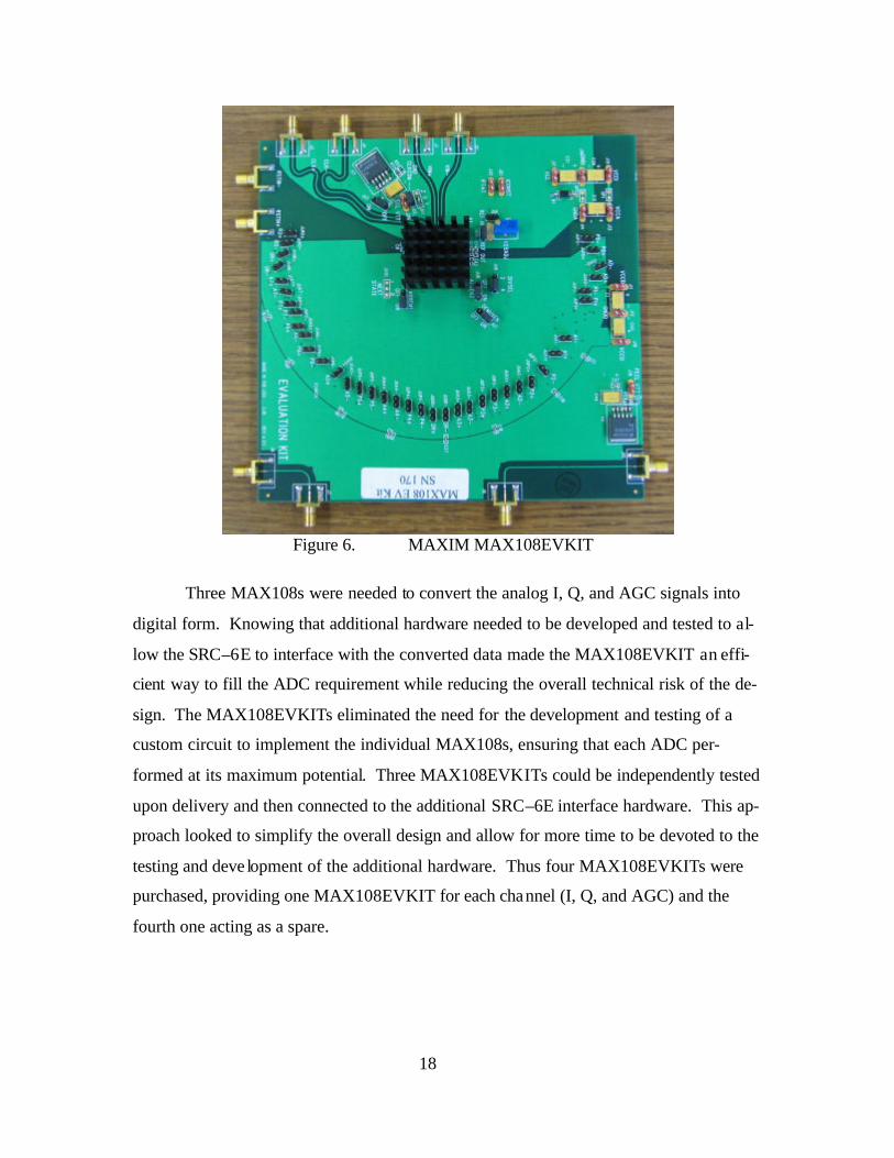
Figure 6. MAXIM MAX108EVKIT
Three MAX108s were needed to convert the analog I, Q, and AGC signals into
digital form. Knowing that additional hardware needed to be developed and tested to al-
low the SRC–6E to interface with the converted data made the MAX108EVKIT an effi-
cient way to fill the ADC requirement while reducing the overall technical risk of the de-
sign. The MAX108EVKITs eliminated the need for the development and testing of a
custom circuit to implement the individual MAX108s, ensuring that each ADC per-
formed at its maximum potential. Three MAX108EVKITs could be independently tested
upon delivery and then connected to the additional SRC–6E interface hardware. This ap-
proach looked to simplify the overall design and allow for more time to be devoted to the
testing and deve lopment of the additional hardware. Thus four MAX108EVKITs were
purchased, providing one MAX108EVKIT for each channel (I, Q, and AGC) and the
fourth one acting as a spare.

19
C. POWER REQUIREMENTS
With a maximum sample clock of 1.5 GHz with 8–bits of resolution, undesired
digital crosstalk may couple through the analog input, power supply, and ground connec-
tions ultimately leading to a possible reduction in the dynamic performance of the ADC
[9]. To avoid this, MAXIM provides very specific guidelines on how the MAX108
should be implemented on a printed circuit board (PCB). The MAX108EVKIT is de-
signed with these specifications in mind and is optimized for minimizing crosstalk from
developing on the board. However, the user must use separate power supplies for the
analog and digital portions of the MAX108 and its accompanying logic to ensure that
crosstalk does not propagate through the power supplies and into the MAX108.
To simplify the implementation and testing of the MAX108, the MAX108EVKIT
reduces the number of individual power connections needed to drive the evaluation
board. To power up the MAX108EVKIT requires two analog power supply connections
(VEE and VCCI) and two digital supplies (VCCD and VCCO). Table 3 lists the power sup-
ply connections, their ground reference, the general circuitry each one is responsible for
powering, and their current requirements. The VCCO supply determines if the digital out-
puts are LVPECL or PECL. By setting VCCO to +3.3V the digital outputs are LVPECL
and by setting VCCO to +5.0 V the digital outputs PECL. The power supply connections
are made via several test points on the MAX108EVKIT. Figure 7 illustrates the general
location of these test points on the MAX108EVKIT and demonstrates a proper power
supply configuration. It is important to note that the analog and digital ground refer-
ences, GNDI and GNDD, respectively, should only be tied together at the power supply.
Once all the power supply connections are made power can be applied to the board to ini-
tiate its operation. [10]

20
Table 3. Power Supply Requirements [9]
Power Supply Connection
Ground Reference
Circuitry Driven Current Requirements
Type
VEE = –5.0 V GNDI Analog circuits –250 mA Analog
VCCI = +5.0 V GNDI T/H amplifier, clock dis-tribution, bandgap refe r-ence, reference amplifier, comparator array
600 mA Analog
VCCD = +5.0 V GNDD All logic circuits of con-verter
250 mA Digital
VCCO = +3.3 –+5.0 V
GNDD Powers all PECL logic sections
600 mA Digital
Figure 7. MAX108EVKIT Power Supply Connections
VEE
GNDI
VCCI VCCA
GNDA
VCCO
VCCD
GNDD
PECL VTT
ECL VTT
VEE 5V
VCCI 5V
- + - +
VCCO 3.3V
VCCD 5V
- + - +
Digital Power Supplies
MAX108EV
Analog Power Supplies

21
D. ANALOG AND CLOCK INPUTS
1. Sample Clock Inputs
The sample clock is brought onto the board via two SMA connectors ( CLK and
CLK ) and is distributed throughout the board via 50 −Ω microstrip transmission lines.
Each clock input is terminated by an on–chip 50 −Ω termination resistor that is con-
nected to a termination path designated as CLKCOM. The CLKCOM termination volt-
age can be connected between ground and –2.0V for compatibility with most standard
ECL devices. The MAX108EVKIT provides an onboard bias generator that generates a
–2.0 V termination voltage from the VEE power supply for connecting the evaluation kit
to ECL clock sources. In the event this onboard termination is not required, CLKCOM
can be connected to ground by connecting the shorting jumper to JU2 and placing JU3 in
its off position on the MAX108EVKIT. [10]
2. Analog Inputs
Two side–launched SMA connectors (VIN+ and VIN–) bring differential or sin-
gle–ended analog signals onto the MAX108EVKIT. Like the clock inputs, the MAX108
provides on–chip 50 −Ω termination to ground for each of the analog input lines. Sam-
pling a differential analog input signal provides the best performance but limits the input
signal amplitude to ± 125 mV. When sampling a single–ended analog input, the input
signal range increases to ± 250 mV. To configure the MAX108EVKIT to accept a sin-
gle–ended analog input, the undriven input (VIN+ or VIN–) needs to be externally re-
verse terminated to GNDI to ensure proper DC balance. [10]
E. DIGITAL OUTPUTS
The MAX108 produces data in offset binary format and routes it to differential
LVPECL/PECL outputs. The output codes vary depending on whether the analog input
is differential or single–ended [10]. Tables 4 and 5 show the input voltage values and the
generated output codes for differential and single–ended inputs, respectively.
The step size for each input configuration was calculated by the following equa-
tion [11]
1
Full-Scale VoltageStep Size ,
2n−= (4.1)

22
where full–scale voltage is the maximum voltage swing of the input signal and n is the
number of bits. Substituting 8 for n and 125 mV for the full–scale voltage yielded a step
size of 0.976 mV for differential inputs. For the single–ended input configuration, the
full scale voltage was increased to 250 mV yielding a step size of 1.95 mV. The output
codes could be converted to the decimal voltage value by converting the unsigned binary
output to decimal and then applying the following equation
( )Signed Voltage Value Converted Decimal 128 Step Size.= − × (4.2)
This binary–to–decimal conversion process worked with either analog input configura-
tion and was essential in testing various components of the interface design for proper
operation.
Table 4. Ideal Input Voltage and Output Code Results for Single–ended Operation (From Ref. 10.)
VIN+ VIN– OVERRANGE BIT
OUTPUT CODE
+125 mV –125 mV 1 11111111 (full scale) +125 mV – 0.5LSB –125 mV + 0.5LSB 0 11111111
0 V 0 V 0 01111111 toggles
10000000 –125 mV + 0.5LSB +125 mV – 0.5LSB 0 00000001
–125 mV +125 mV 0 00000000 (zero scale) Table 5. Ideal Input Voltage and Output Code Results for Single–ended Operation
(From Ref. 10.) VIN+ VIN– OVERRANGE
BIT OUTPUT CODE
+250 mV 0 V 1 11111111 (full scale) +250 mV – 1LSB 0 V 0 11111111
0 V 0 V 0 01111111 toggles
10000000 –250 mV + 1LSB 0 V 0 00000001
–250 mV 0 V 0 00000000 (zero scale)
All the PECL digital outputs are routed on equal–length 50 −Ω microstrip traces
in an arc pattern from the MAX108 to the 2–pin headers as evident in Figure 6. This lay-
out allowed MAXIM to keep the trace lengths to within 0.050 inches of each other
greatly reducing the layout–induced skew amongst the data bits. As Figure 8 demon-

23
strates, the outputs are terminated to the PECL termination voltage just prior to the 2–pin
headers. This places the terminators as close to the receiver as possible before leaving
the board. [10]
Figure 8. MAX108EVKIT Digital Output Termination (From Ref. 10.)
The value of the PECL termination voltage determines if the digital outputs are
PECL or LVPECL providing connection flexibility with +3.3 V and +5.0 V devices. The
LVPECL/PECL termination voltage (PECLVTT) is generated from the VCCO power sup-
ply. Setting VCCO to +5.0 V generates a +3V PECL VTT providing compatibility with
standard PECL devices and setting VCCO to +3.3 V generates a +1.3 V PECL VTT which
allows the outputs to connect to LVPECL devices. [10]
1. Demultiplexer Operation
The MAX108 has an 8–bit primary output port and an 8–bit auxiliary output port.
The converted data is routed to these ports via an internal demultiplexer with three modes
of operation. Table 6 lists the MAX108EVKIT jumpers and the settings required to util-
ize each mode.

24
Table 6. MAX108EVKIT Demultiplexer Jumper Settings [10] Mode Jumper
DIV1 DIV2 DIV4 DEMUXEN OFF ON ON AUXEN2 OFF ON ON AUXEN1 OFF ON ON
DIVSELECT OPEN Position 2 Position 4
a. Non–Demultiplexed Mode
When the demultiplexer is in non-demultiplexed or DIV1 mode, the out-
put is only placed on the primary output port at a maximum sample clock rate of 750
MHz. The sampled data will be repeated on the auxiliary port, but it will be delayed by
one clock cycle. To save power, the auxiliary port can be shut down by connecting the
jumpers AUXEN1 and AUXEN2 to ground. Figure 9 illustrates the timing relationship
between the sample clock, data ready (DREADY), and the output data ports. The
DREADY signal lags the sample clock by half a clock cycle. Data is loaded into the
primary and auxiliary output ports on the falling edge of DREADY 7.5 clock cycles after
the sample was captured. [9]
Figure 9. Non-Demuxed, DIV1 Timing Diagram (From Ref. 9.)
b. Demultiplexed Mode
The demultiplexed or DIV2 mode reduces the output data rate to one–half
the rate of the sample clock. Two consecutive samples are presented on the primary and
auxiliary output ports in a dual 8–bit format. On the rising edge of the data ready clock,

25
the most recent sample is placed on the primary port and the previous sample is placed on
the auxiliary port. The timing for this mode is illustrated in Figure 10. The most current
data is placed on the primary output port and the previous sample is placed on the auxil-
iary port. However, the primary output is only delayed 7.5 clock cycles where the auxil-
iary port is delayed 8.5 clock cycles [9]. The timing diagram also clearly shows how
DREADY operates at half the sample clock rate. By using the DIV2 mode to demulti-
plex the sampled data, the MAX108 is able to sample data at a maximum rate of 1.5
GHz.
Figure 10. Demuxed, DIV2 Timing Diagram (From Ref. 9.)
c. Decimation Mode
The decimation mode or DIV4 mode is a special mode of the MAX108
primarily intended for debugging purposes. When in this mode, every other sample is
discarded as data is placed on the primary and auxiliary output ports at one–fourth the
sample clock rate. A sample clock of 1.5 GHz would place data into each output port at
375 MHz for an effective sampling rate of 750 MHz. Figure 11 shows how DREADY
and the data output rate is reduced to one–fourth the sample clock rate. [9]

26
Figure 11. Decimation, DIV4 Mode Timing Diagram (From Ref. 9.)
2. Data Ready
The MAX108 produces a differential DREADY signal to indicate when the data
in the primary and auxiliary ports is valid. As a digital output, its termination resistor and
termination voltage are exactly the same as the primary and auxiliary output ports. Data
is loaded into the primary and auxiliary output ports on the rising edge of DREADY.
The DREADY signal and the data outputs are internally time aligned by the MAX108,
placing the falling edge of DREADY+ in the center of the valid data window. Triggering
off of the falling edge of DREADY+ in a single–ended configuration or the falling edge
of DREADY in a differential configuration will yield the maximum setup and hold time
for the devices receiving the data. [10]
The data ready clock comes directly from the demux clock generator that creates
the appropriate clocks for the non-demultiplexed and multiplexed modes of operation us-
ing a divide by two circuit. When the MAX108 is powered up, the phase relationship
between the CLK/CLK inputs and the DREADY+/DREADY– outputs is random. As a
result, there is no way to tell if the DREADY clock is in phase with the sample clock or
180 degrees out of phase of the system clock as Figure 12 illustrates. When a single
MAX108 is being used, the phase of DREADY is irrelevant. The most current data will
be on the primary output port and the older data will be on the auxiliary port. However,
when two or more MAX108 are used together to achieve higher sampling rates the order
of samples between devices is critical. Therefore DREADY must be set to a known state
in each MAX108 device. To provide this functionality the MAX108 has a differential

27
PECL reset input (RSTIN) and differential PECL reset output (RSTOUT). The
MAX108EVKIT provides access to these reset pins via 2–pin headers and again handles
the proper LVPECL/PECL termination. To achieve synchronization, a one is applied to
the RSTIN input on the first MAX108 device. The RSTOUT pin of this device is then
connected to the RSTIN of the second device. When the RSTIN signal returns to zero
the phase of the DREADY clock will be reset. [9]
Figure 12. CLK and DREADY Timing in DIV2 mode Showing the Two Possible
Phases of DREADY (From Ref. 9.) F. DESIGN IMPLEMENTATION
1. Input Configuration
The design called for sampling the I and Q channels from the AN/SPS–65 along
with its AGC voltage. Each signal was given its own MAX108EVKIT to facilitate the
analog–to–digital conversion. Since the radar signals were only accessible from single–
ended taps, each MAX108EVKIT was configured to accept single–ended inputs. This
was accomplished by bringing the analog signal in on VIN+ and reverse terminating
VIN– to GNDI via a 50 −Ω terminator attached to the VIN– SMA connector.
2. Sample Clock and Demux Operation
One of the design goals was to sample the 30–MHz I and Q channels from the
AN/SPS–65 using a 200–MHz sample clock generated by the SRC–6E. The MAX108
was more than capable of handling the 200–MHz clock generated by the SRC–6E. How-
ever, the SRC–6E in the SDR mode is limited to accepting data at its system bus speed of

28
100 MHz. To resolve this issue, the MAX108EVKITs were configured to the DIV2
mode of the MAX108 in order to reduce the sampling rate to 100 MHz by placing data
on both the primary and auxiliary output ports. Once captured by the SRC–6E, the data
would be recombined prior to processing.
3. Data Ready
To facilitate a source synchronous data flow into the CHAIN port, the sample
clock generated by the SRC–6E to drive the MAX108s needed to follow with the data
back into the SRC–6E. In addition to having the clock with the data, the SRC–6E needs
a data valid bit to inform it when to latch the data on the CHAIN port. The MAX108-
EVKIT does not have a clock output pin, and to complicate the issue, the 200–MHz sam-
ple clock was twice as fast as the output clock.
To implement source synchronous data flow with the MAX108EVKIT, the
DREADY output from one MAX108EVKIT was used to facilitate the need of a data
valid bit and serve as the source synchronous clock. Since the falling edge of DREADY+
is time aligned to be in the center of the data valid window, all three boards would be
within their valid data window. Any phase delay between the outgoing sample clock
generated by the SRC–6E and the data ready clock would be compensated for by the
DCMs internal to the SRC–6E.
4. Termination and Power Supplies
The SRC–6E does not have onboard termination resistors, thus any signal gener-
ated or received by the CHAIN port needs to be terminated by the external hardware.
With regards to the differential sample clock inputs, the MAX108EVKIT was configured
to use its onboard –2.0 V bias generator and 50 −Ω termination resistors properly termi-
nate the ECL sample clock. This placed the termination for the differential sample clock
as close to the receiver as possible. With regards to the digital PECL outputs, the initial
design called for using the termination resistors that were provided on the MAX108-
EVKIT and using the onboard generated PECL VTT . In the event that distance from the
2–pin header to the chain port proved to be too great for the MAX108EVKIT termination
resistors to be effective, the design could be modified to have the output termination re-
sistors moved from the MAX108EVKIT and placed closer to the CHAIN port. The
VCCO voltage was set to +3.3 V to generate LVPECL outputs.

29
G. INITIAL TESTING AND FAMILIARIZATION
To ensure the MAX108EVKIT would function as the design implementation an-
ticipated, one MAX108EVKIT was connected to the requisite power supplies as shown
in Figure 7. The digital outputs for the primary and auxiliary ports were connected to an
HP 16500B logic analyzer with the clock input connected to DREADY+. The logic ana-
lyzer was then configured to trigger on the falling edge of DREADY+ and the switching
threshold was set to +2.0 V to be compatible with the LVPECL outputs.
The –2.0 V bias generator was left enabled for the clock inputs and the
MAX108EVKIT was placed in DIV2 mode by setting the correct jumpers in accordance
with Table 6. An HP 8082A pulse generator was used to generate a 100–MHz differen-
tial–ECL sample clock and an HP 3312A function generator was used to generate a sin-
gle-ended 1–MHz, 200–mVPP sine wave. With the MAX108EVKIT fully powered up
and both the sample clock and sine wave running into the board, the logic analyzer cap-
tured the demultiplexed digital output and saved it to an ASCII file. The first 600 sam-
ples from this capture are listed in Appendix C and show the DIV2 functioning correctly.
These demultiplexed samples were then recombined in the correct order, converted to the
correct voltage value using Equation 4.2, and then plotted using the MATLAB script
listed in Appendix D. The resulting plot in Figure 13 shows the reconstructed sine wave.
The slight DC offset was a function of the HP 3312A being slightly out of calibration.
This test, though not fully flexing the full capabilities of the MAX108EVKIT, proved the
correct operation of the onboard bias generators, terminators, and correct operation of the
MAX108.

30
0 100 200 300 400 500 600-150
-100
-50
0
50
100
Sample Number
Out
put V
olta
ge (
mV
)
Reconstructed Output from Initial MAX108EV Testing
Figure 13. Reconstructed Output from MAX108EVKIT Testing
H. ADDITIONAL HARDWARE REQUIRED
Though the MAX108EVKITs made maximizing the performance of the MAX108
fairly straightforward, they were not capable of connecting directly to either the
AN/SPS–65 or the SRC–6E. First, the I, Q and AGC signals could only drive a high im-
pedance load, making the 50 −Ω input of the MAX108EVKIT inadequate. In addition,
the ± 5.8 V maximum swing of I and Q plus the 0–12 V range of the AGC voltage were
well above the ± 250–mV input range of the MAX108. Therefore to get the input signals
to the MAX108EVKITs, an analog board needed to be developed to provide the high im-
pedance needed for the input signals while simultaneously attenua ting the three signals to
within the ± 250 mV range.
Next, to be able to get the data from the differential LVPECL outputs into the
SRC–6E, the outputs needed to be translated to single-ended LVTTL. In addition to
translating the signals, a method for connecting the MAX108EVKIT 2–pin headers to the

31
MICTOR connecter used by the SRC–6E CHAIN port needed to be developed. Finally,
the LVTTL sample clock generated by the SRC–6E needed to be translated to ECL and
driven properly to the three MAX108EVKITs.
I. CHAPTER SUMMARY
The MAX108EVKITs provided an efficient and effective way to implement the
required analog–to–digital converters for the design. However, as the previous section
discussed, additional hardware was required to complete the interface between the
AN/SPS–65 and the SRC–6E. The next two chapters discuss the design, development,
and testing of these additional hardware interfaces.

32
THIS PAGE INTENTIONALLY LEFT BLANK

33
V. ANALOG PCB DESIGN
A. INTRODUCTION
The I, Q, and AGC signals from the AN/SPS–65 were well outside the maximum
analog input voltage swing allowed by the MAX108. They also needed to be connected
to a high impedance load whereas the analog inputs of the MAX108EVKITs only offered
a 50−Ω load. Therefore, all three signals needed to buffered and attenuated prior to be-
ing routed to their respective MAX108EVKITs for analog–to–digital conversion. In ad-
dition to having to attenuate the I, Q, and AGC channels, the PRF timing reference signal
needed to be amplified to LVTTL before being sent to the SRC–6E. To help contain the
design to as few boards as possible and reduce the number of power supply connections,
it was decided to perform the attenuation, buffering, and amplification on one single
board.
B. ATTENUATION DESIGN OPTIONS
1. Inline RF Attenuator and Buffer
The first option pursued to attenuate the I, Q, and AGC signals was to run the sig-
nals through a buffer and through an RF attenuator. This method appeared to be the sim-
plest to implement and would provide the best overall frequency response. To see if this
was a feasible option, the attenuation level required to reduce the AGC voltage from its
range of 0 to 12V was calculated using
[ ]Attenuation level dB 20log . in
out
VV
=
(5.1)
Substituting 12 V for Vin and 0.250 V for Vout yielded an attenuation level of 33.62 dB.
A 30–dB RF attenuator in series with 6 dB attenuator would efficiently attenuate the sig-
nal to 190 mV which was well within the ± 250 mV input range of the MAX108.
Due to the large difference between the input and output voltages, the power dis-
sipated was also examined using
( )2
.in outV VP
R−
= (5.2)

34
This yielded 2.76 W in dissipated power which exceeded most RF attenuator power rat-
ings of 1.0 W. RF attenuators that could handle 3.0 W of power were extremely cost
prohibitive. Due to this substantial cost and the desire to implement the same attenuation
scheme on the I, Q, and AGC signals, the RF attenuator option was deemed unacceptable
for this design.
2. Op–Amp Attenuation Circuit
The next attenuation design considered was to again run the signals into a high–
speed buffer and then into a high–speed op–amp circuit with a gain less than one. The
buffer would provide the required high input impedance while the fractional gain would
attenuate the signal to the appropriate level and drive the low load impedance. Again, the
design goal was to use the same overall circuit design for the I, Q, and AGC signals.
Though the signal bandwidth of I and Q was 30.13 MHz, the attenuation circuit was de-
signed to have at least 200 MHz of analog signal bandwidth for the possibility of inter-
facing with radars other than the AN/SPS–65. In addition, the minimum slew rate (S)
required to drive the ± 250–mV outputs at 200 MHz was determined from [11]
2 .SR oS f Vπ= (5.3)
Substituting 200 MHz for the slew rate limiting frequency (fSR) and 250 mV for the maxi-
mum output voltage (Vo) yielded a minimum slew rate of 315 V µs.
The gain required for the I and Q channels was –0.043 and the gain required for
the AGC voltage was –0.021. The power supply rails needed to be greater than 7.8 V and
greater than 14 V for the AGC voltage to avoid saturation for the I and Q channels. Sev-
eral high–speed op–amps could provide the needed slew rate and analog bandwidth.
However, no high–speed op–amp could be found to drive a negative gain of less than one
and at the same time drive a 50 −Ω load with power rails in excess of ± 5.8 V. To be
able to use the commercially available high–speed op–amps, the I, Q, and AGC signals
needed to be attenuated prior to being buffered.

35
3. Voltage Divider to High–Speed Buffer
To achieve high input impedance attenuation, each signal was routed through a
simple two–resistor voltage divider prior to entering a high–speed buffer. Figure 14 illus-
trates the general voltage divider and buffer circuit implemented in the design.
Figure 14. Two–Resistor Voltage Divider and Buffer Circuit
The resistor R1 was set to 10 kΩ to provide the requisite high input impedance for
the AN/SPS–65 signals. As an added measure of safety, the I, Q, and AGC signals were
attenuated to ± 225 mV to ensure that the analog inputs of the MAX108 were not over-
driven. The resistor R2 was then calculated to provide the appropriate attenuation for the
I, Q, and AGC signals using
.out
in out
V R1R2
V V=
− (5.4)
Table 7 lists the calculated and selected R2 resistors values for the I, Q, and AGC voltage
dividers.
Table 7. Resistor Values for Voltage Divider
Signal Vin (V) Vout (V) Selected R1 Value (kΩ )
Calculated R2 Value (Ω )
Selected Standard R2 Value (Ω )
I ± 5.8 0.225 10.0 403.59 402.0
Q ± 5.8 0.225 10.0 403.59 402.0
AGC 12.0 0.225 10.0 191.08 191.0

36
With the I, Q, and AGC voltage signals attenuated to ± 225 mV, an appropriate
buffer needed to be selected to drive the 50 −Ω analog inputs of the MAX108EVKITs.
The power rails for this high–speed buffer were set to ± 5 V in an effort to reduce the
number of power supplies employed in the overall interface design. Since a positive and
negative power rail was required to handle the voltage swing of the analog signals, the
analog board could easily connect to the ± 5 V supplies already needed to power the
three MAX108EVKITs.
The LMH6559 high–speed closed loop buffer was the only buffer at the time of
design that could meet the analog signal bandwidth, slew rate, and power supply re-
quirements. The LMH6559 offered a small–signal bandwidth of 1750 MHz, a 4580
V µs slew rate, and could be powered by ± 5 V. It also had a 200– kΩ input impedance
and a 1.2 −Ω output impedance, making it ideal for driving the analog inputs of the
MAX108EVKITs. [12]
To verify that the buffer would perform as expected driving a 50 −Ω load, the
LMH6559 performance was simulated using Silvaco® SmartSpice®. The LMH6559
spice model was downloaded from the National Semiconductor website and implemented
in the SPICE deck shown in Appendix E. The source signal was a 0.225–V AC signal
that was swept from 0 to 500 MHz. To simulate driving the MAX108EVKIT analog in-
puts, the output of the LMH6559 was connected to a 50 −Ω resistor to ground. The re-
sults of the simulated AC sweep are shown in Figure 15.

37
0 50 100 150 200 250 300 350 400 450 5000.15
0.16
0.17
0.18
0.19
0.2
0.21
0.22
0.23AC Sweep of LMH6559
Frequency (MHz)
Vol
tage
(V
)
Figure 15. AC Sweep Analysis of the LMH6559
The results depicted in Figure 15 show the frequency response degrading linearly
as the frequency exceeds 150 MHz. Since 150 MHz was still well above the 30.13 MHz
bandwidth of the AN/SPS–65, it was determined that the LMH6559 would provide the
desired performance. In addition, the accuracy of the model with a small load resistance
was questioned since the LMH6559 has a 1750–MHz small–signal bandwidth and gain
flatness up to 200 MHz when the output voltage is less than 0.5 Vpp. Therefore, the de-
sign went forward with using the LMH6559 high–speed buffer. [12]
C. PRF TIMING REFERENCE AMPLIFICATION DESIGN
At the time of the analog board design, the PRF timing reference signal was
thought to be a square pulse signal that ranged from 0 to 1.0 V. To amplify the 1.0 V
signal to the 3.3 V level of LVTTL, a non–inverting op–amp with a gain of 3.3 was used.
Once amplified to LVTTL, the PRF timing reference signal only required source–series

38
termination prior to connecting to the SRC–6E. Therefore, the design placed a 50 −Ω
resistor in series with the output of the amplifier circuit to properly terminate the signal.
Figure 16 shows the PRF timing reference amplification circuit implemented in the de-
sign.
Figure 16. PRF Timing Reference LVTTL Amplification Circuit
The design of the attenuation and buffering circuit for the I, Q, and AGC signals
set the power rails to ± 5 V and most op–amps operating with these power supplies could
handle the 3063–Hz analog bandwidth of the PRF timing reference signal. The deciding
factor for the op–amp to place in this circuit was its ability to source 66 mA continuously
over the source–series termination resistor. The LMH6642 operational amplifier selected
for the design provided rail–to–rail performance capable of driving 75 mA to the load. It
also provided analog signal bandwidth of 15 MHz with a gain of +5 making it capable of
interfacing to radars with much higher PRFs [13].
Using
1 ,V
R12A
R1= + (5.5)
standard resistor values were selected to provide a nominal gain of 3.3 (AV). With R12
set to 2.74 kΩ and R10 set to 1.21 kΩ , the circuit produced a gain of 3.26 which was

39
adequate enough for the LVTTL requirements of the SRC–6E. The resistor R11 was
placed to ensure proper DC biasing. Its value was determined by calculating the equiva-
lent parallel resistance of R12 and R10. The capacitor C17 was inserted as a place holder
in the event the circuit needed to be stabilized [13].
The circuit was simulated in SmartSpice using the SPICE deck in Appendix F. A
1.0–V 3063–Hz signal representing the PRF timing reference was connected to the input
of the circuit and the output was connected to a 50 −Ω resistor to ground to represent the
source–series termination resistor. Figure 17 plots both the simulated PRF timing refer-
ence signal and the resulting output waveform illustrating the correct operation of the cir-
cuit.
0 0.1 0.2 0.3 0.4 0.5 0.6 0.7 0.8 0.90
0.5
1
1.5
2
2.5
3
3.5
4Simulation of PRF Amplifier
Time (ms)
Vol
tage
(V
)
PRF from AN/SPS-65PRF LVTTL Out
Figure 17. Simulation of PRF Timing Reference Amplifier Circuit

40
D. PCB DESIGN AND LAYOUT
Initially, the design sought to assemble all the necessary components for any cus-
tom built hardware by wire–wrapping them to a protoboard. This would allow for rapid
assembly and allow the design to be easily modified to rectify design errors. However,
the components selected for the analog board and the translation board discussed in the
following chapter only came in surface–mount packages. The number of test sockets re-
quired for the design became cost prohibitive and the parasitic capacitance that the test
sockets would have induced could have degraded the quality of the high–speed data sig-
nals being analyzed. Ultimately, the MICTOR connecter used to connect the radar inter-
face to the SRC–6E made wire–wrapping impossible, driving the design to use printed
circuit boards.
1. PCB Software Selection
The circuit boards needed for the design were not extremely complex, requiring
power and ground planes with all signal traces running along the surface. Several evalua-
tion or free versions of PCB software were examined to see if they would meet the needs
of the design. However, most were limited to a maximum size of 3′′ by 5′′ , supported no
more than 30 components and allowed no more than two layers. The exception to theses
limitations was the software available from ExpressPCB™. The ExpressPCB free soft-
ware, downloadable from www.expresspcb.com, offered a schematic editor that was link-
able to their printed circuit board CAD drawing tool. The CAD program allowed two
and four layer boards up to 12′′ by 14′′ in size. There was no limitation on the number of
components implemented and the manufacturing specifications listed in Appendix G
were adequate to facilitate the components implemented in the design [14]. The only
tradeoff to using the software from ExpressPCB was that the printed circuit boards had to
be manufactured through them. The cost to fabricate a board through ExpressPCB was
comparable to other PCB fabrication houses. Thus, it was decided to use ExpressPCB to
design and fabricate the required PCBs for the interface design.
2. Analog Board Schematic Layout
Using the ExpressSCH schematic editor from ExpressPCB, the circuits in Figure
14 and Figure 16 were drawn. In accordance with the application notes for the LMH6643
and LMH6659, both power supply rails were connected to two bypass capacitors. The

41
capacitors used were a 0.01 µF and a 0.1 µF with the 0.01 µF being placed closest to the
device. The input and output of each circuit along with the +5 V and –5V supplies were
connected to 50 −Ω SMA connecters to provide clean and flexible connections. A sepa-
rate SMA connector wired to ground was also provided to provide an accessible test point
to connect probe ground leads. Figure 18 shows the complete analog board schematic.

42
Figure 18. Complete Analog Board Schematic

43
3. Analog Board PCB Design
The analog board was implemented on a four–layer board for two reasons. First,
since the ground plane and one power plane would be placed on the two inner layers, the
top surface layer would be free to route the input, output, and feedback signals. Second,
the four–layer board offered trace widths with impedances of about 50 Ω .
Both the MAX108EVKITs and SRC–6E CHAIN port interface require 50 −Ω ter-
mination and 50 −Ω transmission lines, therefore it was extremely important for the
PCBs used in the interface design to implement traces as close to 50 Ω as possible. Prior
to conducting any component and trace placement, the impedances of various trace
widths for four layer boards from ExpressPCB were calculated using [15]
( )
5.9887ln
0.8.
1.41or
dw t
Zε
+ =
+ (5.6)
In Equation 5.6, d represents the distance to the ground plane, w represents the trace
width, t is the trace thickness, and rε is the dielectric constant of the material used in the
circuit board. From Appendix G, d was determined to be 0.012′′ , t was 0.014′′ , and rε
was 4.6 0.02± . These values were substituted into Equation 5.6 and solved for various
trace widths. Table 8 lists the trace widths and their corresponding impedances.
Table 8. Trace Impedance Calculation Results Trace Width (Mils)
Zo Imped-ance (Ohms)
7 82.6 8 78.8 10 72.1 12 66.6 15 59.6 20 50.28 25 42.9 30 36.9
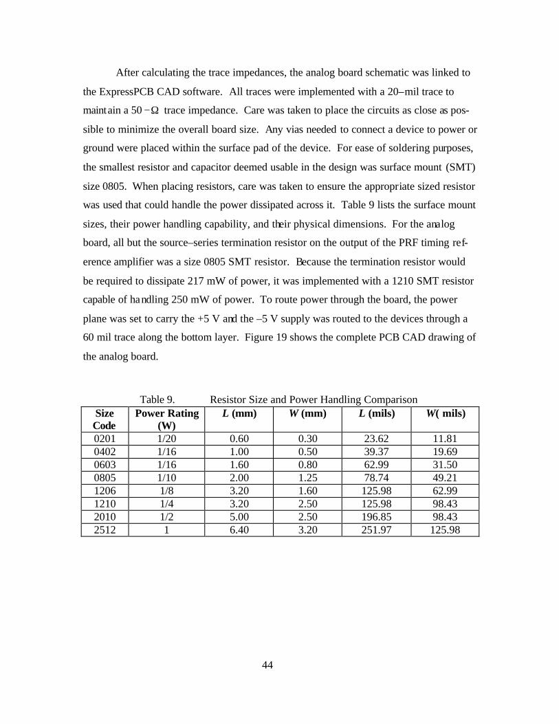
44
After calculating the trace impedances, the analog board schematic was linked to
the ExpressPCB CAD software. All traces were implemented with a 20–mil trace to
maintain a 50 −Ω trace impedance. Care was taken to place the circuits as close as pos-
sible to minimize the overall board size. Any vias needed to connect a device to power or
ground were placed within the surface pad of the device. For ease of soldering purposes,
the smallest resistor and capacitor deemed usable in the design was surface mount (SMT)
size 0805. When placing resistors, care was taken to ensure the appropriate sized resistor
was used that could handle the power dissipated across it. Table 9 lists the surface mount
sizes, their power handling capability, and their physical dimensions. For the analog
board, all but the source–series termination resistor on the output of the PRF timing ref-
erence amplifier was a size 0805 SMT resistor. Because the termination resistor would
be required to dissipate 217 mW of power, it was implemented with a 1210 SMT resistor
capable of handling 250 mW of power. To route power through the board, the power
plane was set to carry the +5 V and the –5 V supply was routed to the devices through a
60 mil trace along the bottom layer. Figure 19 shows the complete PCB CAD drawing of
the analog board.
Table 9. Resistor Size and Power Handling Comparison Size Code
Power Rating (W)
L (mm) W (mm) L (mils) W( mils)
0201 1/20 0.60 0.30 23.62 11.81 0402 1/16 1.00 0.50 39.37 19.69 0603 1/16 1.60 0.80 62.99 31.50 0805 1/10 2.00 1.25 78.74 49.21 1206 1/8 3.20 1.60 125.98 62.99 1210 1/4 3.20 2.50 125.98 98.43 2010 1/2 5.00 2.50 196.85 98.43 2512 1 6.40 3.20 251.97 125.98

45
Figure 19. PCB CAD Drawing for Analog Board
E. TESTING
Prior to assembling the board, all traces were tested with an ohm meter to ensure
trace continuity and to test for possible shorts on the board. After all traces and power
planes appeared error free, the components were soldered to the board. Once assembled,
power was applied to the board to verify that no shorts were present between the power
and ground connections. Figure 20 shows the fully assembled analog board.
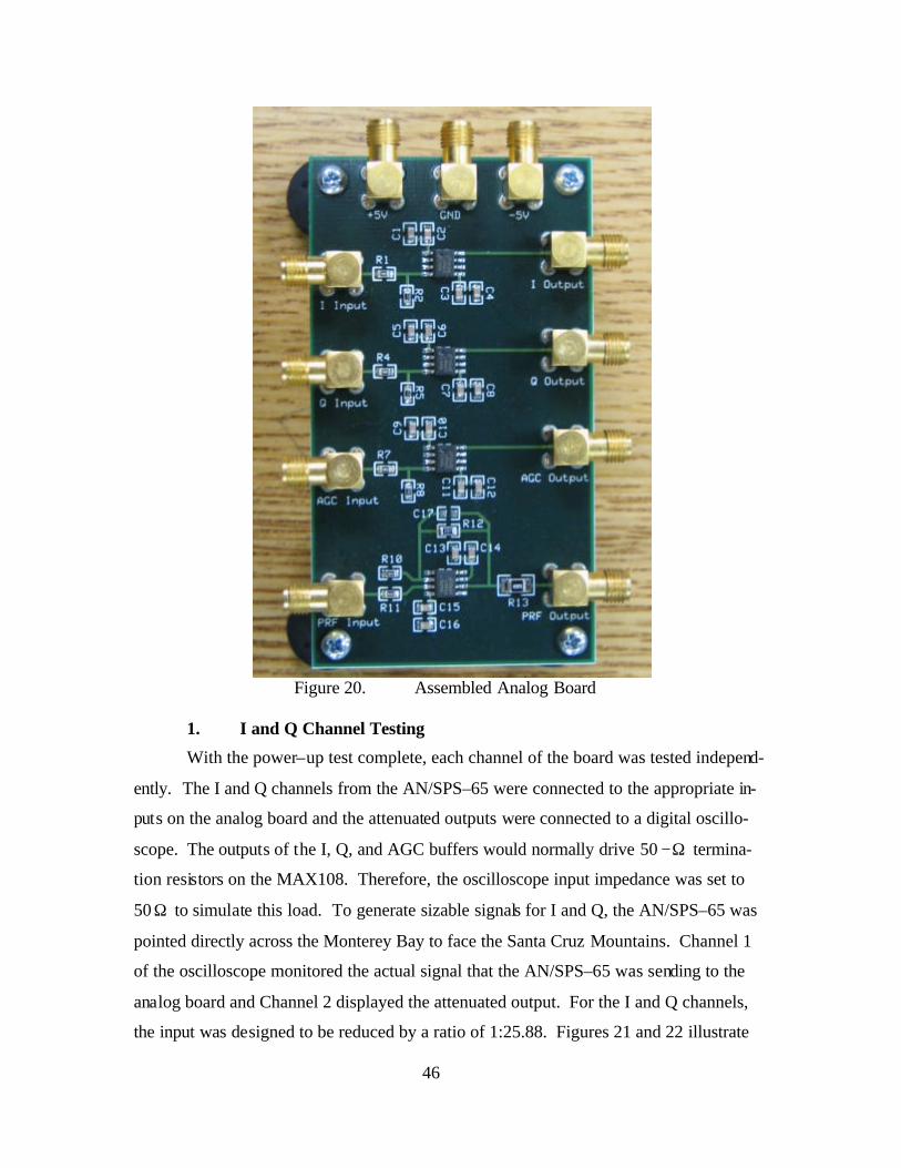
46
Figure 20. Assembled Analog Board
1. I and Q Channel Testing
With the power–up test complete, each channel of the board was tested independ-
ently. The I and Q channels from the AN/SPS–65 were connected to the appropriate in-
puts on the analog board and the attenuated outputs were connected to a digital oscillo-
scope. The outputs of the I, Q, and AGC buffers would normally drive 50 −Ω termina-
tion resistors on the MAX108. Therefore, the oscilloscope input impedance was set to
50 Ω to simulate this load. To generate sizable signals for I and Q, the AN/SPS–65 was
pointed directly across the Monterey Bay to face the Santa Cruz Mountains. Channel 1
of the oscilloscope monitored the actual signal that the AN/SPS–65 was sending to the
analog board and Channel 2 displayed the attenuated output. For the I and Q channels,
the input was designed to be reduced by a ratio of 1:25.88. Figures 21 and 22 illustrate

47
the proper attenuation of the I and Q channels, respectively. The maximum voltage peak
on the input for both channels was 250 mV which was correctly attenuated to 10 mV on
both circuits. In addition, Figures 21 and 22 illustrate that the I and Q circuits have the
needed frequency response as the output data tracks the input data exactly.
Figure 21. Test of I Channel Attenuation Circuit

48
Figure 22. Test of Q Channel Attenuation Circuit
2. AGC Voltage Testing
The AGC voltage on the AN/SPS–65 used by the Naval Postgraduate School is
set a fixed value of 10.0 V. It was connected to the appropriate input on the analog board
and the oscilloscope input impedance remained set at 50 Ω to simulate the termination
resistor on the MAX108. Figure 23 shows the AGC voltage was correctly scaled by a
ratio of 1:55.36 from 10 V down to 186 mV.

49
Figure 23. Test of AGC Voltage Attenuation Circuit
3. PRF Timing Reference Testing
The PRF timing reference signal testing was conducted in the same manner as the
previous three signals except the oscilloscope input impedance was set to 1 MΩ . This
was necessary because the output of the PRF timing reference amplifier was already con-
nected to a 50 −Ω load. As Figure 24 illustrates, the PRF timing reference was amplified
by a factor of 3.3. However, the amplified PRF timing reference output was 3.56 V in-
stead of 3.26 V as designed. This was a result of the PRF timing reference signal actually
having a maximum value of 1.1 V instead of the 1.0 V the design anticipated. Not want-
ing to overdrive the LVTTL logic in the SRC–6E, the amplifier was modified to reduce
the overall gain from 3.26 to 2.9. This was accomplished by replacing the 2.74 k− Ω
feedback resistor with a 2.3 k− Ω feedback resistor. With a gain of 2.9, the resulting am-
plified PRF timing reference signal was 3.19 V, which is still a valid LVTTL signal.
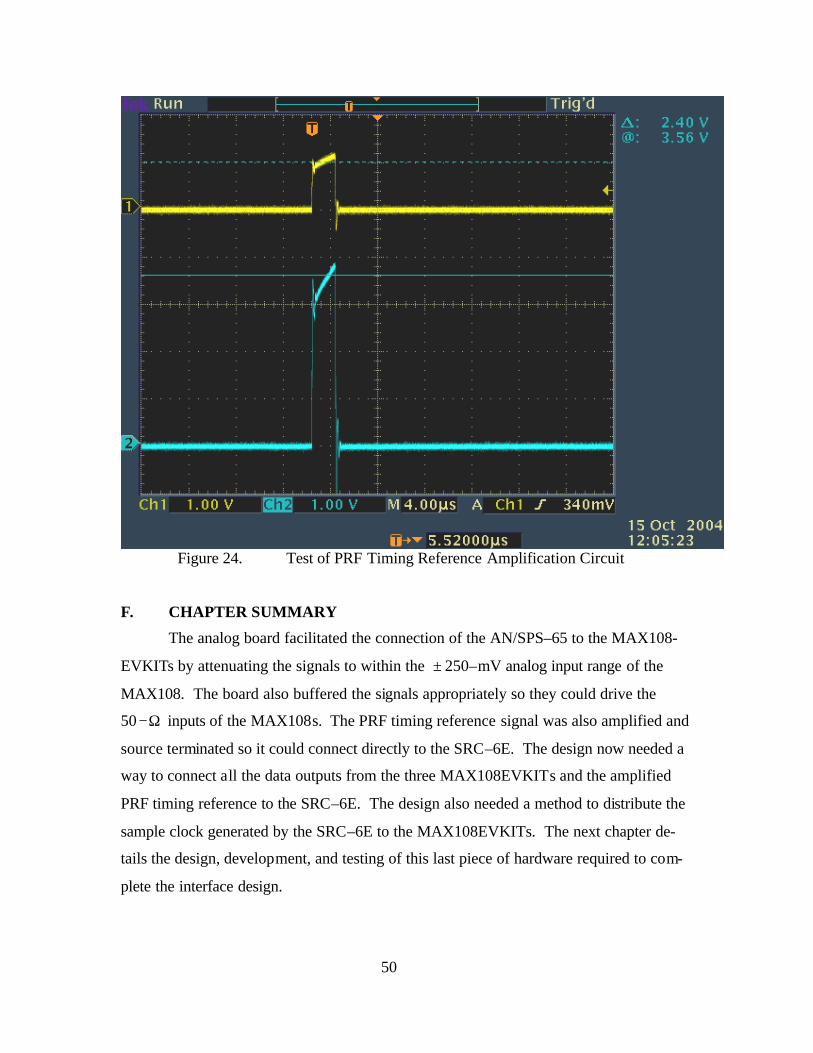
50
Figure 24. Test of PRF Timing Reference Amplification Circuit
F. CHAPTER SUMMARY
The analog board facilitated the connection of the AN/SPS–65 to the MAX108-
EVKITs by attenuating the signals to within the ± 250–mV analog input range of the
MAX108. The board also buffered the signals appropriately so they could drive the
50 −Ω inputs of the MAX108s. The PRF timing reference signal was also amplified and
source terminated so it could connect directly to the SRC–6E. The design now needed a
way to connect all the data outputs from the three MAX108EVKITs and the amplified
PRF timing reference to the SRC–6E. The design also needed a method to distribute the
sample clock generated by the SRC–6E to the MAX108EVKITs. The next chapter de-
tails the design, development, and testing of this last piece of hardware required to com-
plete the interface design.

51
VI. TRANSLATION BOARD DESIGN
A. INTRODUCTION
The MAX108EVKITs converted the analog I, Q, and AGC voltage signals into
digital form and presented the data using LVPECL logic levels onto 2–pin headers. For
the SRC–6E to use these signals, they needed to be connected to a 114–pin MICTOR
connector and converted from LVPECL to LVTTL. The amplified PRF timing reference
signal from the analog board also needed to be connected to the MICTOR connector
while the sample clock generated by the SRC–6E needed to be converted from LVTTL to
ECL to drive the MAX108EVKITs. To facilitate this signal translation and mate the sig-
nal lines to the MICTOR connector, a single translation board was developed.
B. SIGNAL TRANSLATION
1. LVPECL–to–LVTTL Translation
To effectively convert the 49 differential LVPECL data outputs of the three
MAX108EVKITs to LVTTL for use in the SRC–6E, it was decided to use commercial–
off–the–shelf LVPECL–to–LVTTL translator ICs. The use of a translator IC would in-
crease the propagation delay of the signal, so care was taken to select a translator chip
that had an extremely small propagation delay. In addition, the translator needed to be
capable of handling a 200–MHz signal to allow future work with the interface using the
DDR capability of the SRC–6E.
Though multiple LVTTL–to–LVPECL translators could be found, only On Semi-
conductor produced LVPECL–to–LVTTL translators that met the design requirements.
The MC100EPT21 and MC100EPT23 provided an operating frequency in excess of 275
MHz, used a single 3.3–V power supply, and only imposed a typical propagation delay of
1.5 ns. The difference between the two 8– pin translators was that the MC100EPT21
could only handle a single differential pair, while the MC100EPT23 came in a dual dif-
ferential configuration. The MC100EPT23 was selected for the design because the abil-
ity to translate two differential pairs cut the number of chips required in half and greatly
reduced the surface area required for the translation board.

52
2. LVTTL–to–ECL Translation
Having handled the translation from LVPECL to LVTTL for the data inputs into
the SRC–6E, the next design step was to select an adequate LVTTL–to–ECL translator to
convert the LVTTL sample clock generated by the SRC–6E to the ECL clock required by
the MAX108EVKITs. As with the selection of the LVPECL–to–LVTTL translators, the
design looked to maintain compatibility with the DDR mode of the SRC–6E. Therefore,
the clock translator needed to be capable of translating a 400–MHz sample clock which
was twice the design frequency of 200 MHz. Once translated, the clock signal needed to
pass through a clock driver to effectively distribute the clock to all three MAX108-
EVKITs.
The MAXIM MAX9360 LVTTL–to–ECL translator, designed for high–speed
clock and data distribution, was selected to perform the sample clock translation. With a
maximum frequency of 3 GHz, the MAX9360 converts a single–ended LVTTL input to a
differential–ECL output with a typical propagation delay of 440 ps. A +3.3 V and a –5 V
are required to facilitate the translation between the two logic standards. Though the in-
ternal circuitry of the MAX9360 is capable of being a clock driver, it can only drive one
clock. Therefore an additional clock driver was still needed. [17]
A clock driver with at least three differential outputs was required to ensure that a
clean and low–skew clock signal was delivered to the three MAX108EVKITs. The
MAX9316A 1:5 differential clock driver solved the clock distribution problem. Using a
single –5–V supply, it can drive a 1.5–GHz differential clock to five separate devices
while imposing only a 365–ps delay. With two extra outputs available, the design used
one to provide a test clock and the other was terminated to ground. [18]
C. MICTOR CONNECTOR ALTERNATIVES
As discussed in Section D of Chapter V, the design sought to assemble all custom
hardware on a proto–board and then wire–wrap the components together. Though the
surface–mount ICs selected for the design could be implemented with test sockets, the
AMP MICTOR connector used by the SRC–6E could not. The 114 pins of the connector
had 0.025–inch centerlines with the ground pins protruding from the center of the con-

53
nector with no known test socket available [19]. In order to wire–wrap the data lines to a
connector, the connector pins needed to have 0.100–inch centerlines. Before leaving the
wire–wrap implementation for PCB design, two other alternatives to the surface–mount
MICTOR connector were pursued.
1. Custom Micro–Coaxial Cable
SRC Computers, Inc. provided the project with four 48–inch–long micro–coaxial
cables with the requisite push–in connector for the MICTOR connector on each end. The
micro–coaxial cable mates to the push–in connector through an extremely small PCB that
connects the 114 pins of the connector to the individual signal lines. Precision Intercon-
nect manufactured the cables used by SRC Computers and was contacted to see if they
could make a custom cable with a push–in MICTOR connector on one end and a 0.100–
inch header connector on the other. A custom cable of this type was possible, but due to
the automated process involved a small run of a few cables would cost well over
$2,000.00. The simplicity of implementation that this custom cable would have provided
was not enough to justify the cost and was eliminated as a possible alternative.
2. MICTOR Connector Breakout Adapter
The next alternative considered was an adapter that would breakout the 114 pins
of the MICTOR connector from their 0.025–inch spacing to individual pins with 0.100–
inch spacing. This would allow the design to utilize the micro–coaxial cable provided by
SRC Computers while still affording the capability to wire–wrap the requisite connec-
tions on a proto–board. Again the need for only one breakout adapter and the cost of the
surface–mount MICTOR connector itself prevented this from being a viable alternative.
3. Printed Circuit Board Implementation
Without a cost effective method to wire–wrap a connector capable of connecting
to the micro–coaxial cable of the SRC–6E, the surface–mount MICTOR connector
needed to be implemented on a PCB. The manufacturing specifications provided by Ex-
pressPCB in Appendix G were sufficient to handle the pitch of the surface–mount
MICTOR connector. In addition, the ExpressPCB software discussed in Chapter V al-
lowed the design of custom device footprints. Using the data from Reference 19 and the
schematic shown in Appendix H, the appropriate device footprint was constructed for the
surface–mount MICTOR connector for use in the translation board PCB layout.

54
As with the breakout adapter alternative, the cost of an individual MICTOR con-
nector was still an issue. At the time of design, no supplier could be located that would
sell a low volume order of less than 35 connectors. At an average price of $50.00 per
connector, the design budget could not afford to purchase a large number of connectors.
To avoid incurring this sizable cost, a sample MICTOR connector was obtained from
Tyco Electronics for implementation in the design.
D. MAX108EVKIT–TO–TRANSLATION BOARD CABLING
The design implementation of the three MAX108EVKITs produced 49 differen-
tial pairs of LVPECL outputs for a total of 98 individual signals that needed to be con-
nected to the translation board. To interface the MAX108EVKITs to the translation
board, the design used 34–position 0.1′′ by 0.1′′ low–profile headers from 3M Intercon-
nect to provide a compact arrangement of 2–pin headers on the translation board. The I,
Q, and AGC voltage signals each used two of these headers to handle the demultiplexed
data coming from the MAX108EVKITs.
To maintain a 50 −Ω signal path from the 2–pin headers on the MAX108EVKITs
to the headers on the translation board, the design sought to implement shielded
50 −Ω coaxial cables terminated at each end by 2–pin connectors. However, no cable
manufacturer could be found that offered pre–made coaxial cable in this configuration.
Custom cables could have been fabricated, but again the cost for such cables outweighed
the convenience they would provide. Since coaxial cable was not a feasible option, the
design selected shielded controlled impedance (SCI) cables manufactured by 3M Inter-
connect. Designed specifically to connect to standard 2–pin headers, these cables were
offered in two 50 −Ω variations and one 75 −Ω variation with user specified lengths.
Table 10 lists the electrical properties for each type. To keep the transmission path as
short as possible yet still be able to connect all three MAX108EVKITs to the translation
board, a cable length of 10 inches was selected. The cost per cable for type 017 was
$15.31 and it was $16.61 for the type 027. Since the type 027 was only $1.30 more than
the type 017 and provided better performance, the type 027 cable was selected for the de-
sign. Figure 25 illustrates the cable implemented in the design. Though these cables

55
were still relatively expensive, they were the most cost–effective option available to meet
the design requirements. [20]
Table 10. Shielded Controlled Impedance Cable Electrical Properties (From Ref. 20.)
Electrical Properties (TYP) Cable Type Capacitance Propagation
Delay Attenuation Conductor Resis-
tance 017 50
5 Ω
± Ω
32 pf/ft max (105 pf/m)
1.46 ns/ft nom (4.8 ns/m)
33 dB Max/100 ft @ 400 MHz
(108 dB/100 m)
0.24 /ftΩ at 68 F° (0.8 / mΩ at 20 C° )
027 50 2
Ω± Ω
23 pf/ft nom
(75 pf/m) 1.15 ns/ft nom
(3.77 ns/m) 20 dB Max/100 ft @ 400 MHz Nom
(65 dB/100 m)
0.041 /ftΩ at 68 F° (0.15 / mΩ at 20 C° )
041 75 3
Ω± Ω
16 pf/ft max
(52 pf/m) 1.22 ns/ft nom
(4.0 ns/m) 10 dB Max/100 ft
@ 100 MHz (33 dB/100 m)
0.09 /ftΩ at 68 F° (0.3 / mΩ at 20 C° )
Figure 25. Shielded Controlled Impedance Cable
E. PCB DESIGN AND LAYOUT
1. Initial Design Considerations
Due to the number of signal traces involved and the need to maintain a trace im-
pedance of 50 Ω , the translation board was designed on a four–layer PCB. As Table 8 in
Chapter V illustrated, trace widths of 15 mils and 20 mils on a four–layer board have an
impedance of 60 Ω and 50 Ω , respectively. Keeping the trace impedance of the data
lines as close as possible to 50 Ω was essential to minimizing reflections that can distort
the data. The four–layer board also allowed the primary voltage source to be imple-
mented as a power plane and thus greatly increased the amount of board area available
for device placement and trace routing.

56
To provide clean connections to the board all power supply inputs, clock outputs,
and the PRF timing reference input were implemented using right–angle SMA connec-
tors. The SMA connectors provided a reliable 50 −Ω connection to the translation board
and required a relatively small footprint on the PCB. In an attempt to keep all traces to
the MICTOR connector the same length, the MICTOR connector was located in the cen-
ter of the translation board. As Figure 26 illustrates, the data lines connect to the
MICTOR connector from both sides keeping all the traces on the top layer of the board.
The signals from one side of the connector could have been routed to the other side by
using vias to traverse the layers of the board. However, each via induces a small amount
of parasitic capacitance onto the trace, slowing down the signal. Keeping the traces on
the top layer ensured that the cleanest signal path was achieved.
Figure 26. Block Diagram of Translation Board and MAX108EVKIT Arrangement
2. Device Termination
All of the signal paths in the design between the analog board and the MICTOR
connector had to be properly terminated. The PRF timing reference signal was already
source–series terminated on the analog board and the MAX108EVKITs provided on-
board termination for both its inputs and outputs. The translation board thus needed to
provide the appropriate termination for the implemented devices on the translation board
itself. In addition, the translation board needed to provide for termination for both the
LVPECL inputs and ECL clock outputs in the event that the terminators of the MAX108-
EVKIT were ineffective.
MICTOR
MAX108EV
MAX108EV
MAX108EV
Translation Board
17 Data Lines 16 Data Lines
16 Data Lines

57
The LVPECL–to–LVTTL translators on the translation board needed to be
source–series terminated to 50 −Ω terminations prior to connecting to the MICTOR con-
nector. Since the output impedance of a TTL circuit varies depending if it is transmitting
a high or low, a 50 −Ω resistor could not just be simply placed in series with the output.
The MC100EPT23 has an output impedance of 5 Ω when transmitting a logic high and an
output impedance of 15 Ω when transmitting a logic low [21]. The average output im-
pedance of 10 Ω was assumed to be the output impedance of the device. Therefore, a
40 −Ω resistor was placed in series with the output to produce the 50 Ω source–series
termination.
The RC shunt termination required for the SRC–6E sample clock was imple-
mented as recommended by SRC Computers. A 50 −Ω resistor in series with a
0.01 µF capacitor was tied to ground prior to the LVTTL clock entering the MAX9360
LVTT–to–ECL translator. The differential output of the MAX9360 was terminated to
–2V through 50 −Ω resistors. All of the outputs of MAX9316A clock driver had pads
placed for terminating the outputs to –2V through 50 −Ω resistors with the intent of only
terminating the unused output. The additional pads were placed in the event that testing
showed the termination resistors for the clock inputs on the MAX108EVKITs were inef-
fective. This was highly unlikely because having the terminators on the MAX108EVKIT
clock inputs placed them as close to the receiver as possible which is the ideal termina-
tion configuration.
Similarly, pads for 50 −Ω resistors connected to +1.3 V were placed on the inputs
to the MC100EPT23 translators in case the signal path between the outputs of MAX108-
EVKITs and inputs on the translation board was too long for the termination resistors on
the MAX108EVKITs to effectively terminate the signal. If this was the case, the termi-
nation resistors could be removed from the MAX108EVKITs and placed on the transla-
tion board. This would then place the terminators as close to the receiver as possible,
creating an optimum termination configuration.
To ensure the correct size of the SMT termination resistor was selected, the power
dissipated over each termination resistor was calculated as

58
( )2
.Ox ref
term
V VP
R
−= (6.1)
The value VOx represents the largest output voltage seen at the resistor, Vref is the refer-
ence voltage, and Rterm is the termination resistor value. Table 11 lists the power dissi-
pated over each termination resistor and the size of resistor selected.
Table 11. Termination Resistor Power Calculations Terminator VOx Vref Rterm Power Resistor Size LVPECL to LVTTL Input 2.5 V 1.3 V 50 Ω 0.029 W 0805 LVTTL to MICTOR 3.3 V 0.0 V 45 Ω 0.242 W 1210 ECL DeviceTermination –0.865 V –2.0 V 50 Ω 0.026 W 0805
3. Power Distribution
To determine what voltage to assign to the power plane, the power requirements
for all the devices to be implemented on the translation board were tabulated in Table 12.
In addition to the individual device requirements, the table also includes the –2.0 V and
+1.3 V termination voltages needed on the board using the total number of termination
resistor pads implemented to calculate the total possible required current.
Table 12. Translation Board Voltage and Current Requirements Device Quantity Voltage Max Current Total Current
MC100EPT23 25 3.3 V 33 mA 825 mA MAX9360 1 3.3 V 7 mA 7 mA MAX9360 1 –5.0 V 20 mA 20 mA MAX9316A 1 –5.0 V 40 mA 40 mA –2.0V ECL Termination Voltage
12 –2.0 V 23 mA 276 mA
1.3 V LVPECL Termination Voltage
98 1.3 V 24 mA 2.352 A
The initial testing of the design intended to use the onboard termination resistors
of the MAX108EVKITs, which would eliminate the immediate need to have a power
plane dedicated to either the –2.0 V or 1.3 V termination voltages. Also, the termination
resistors were concentrated at the edges of the board allowing the use of a wide trace

59
along the bottom layer of the board. The power required by the two –5.0–V devices was
dwarfed by the large number of devices requir ing 3.3 V. The 26 3.3–V devices were to
be located throughout the board and required a significant amount of current. Therefore,
the power plane was set to 3.3 V and traces of sufficient width were used to route power
to the devices requiring –5.0 V.
4. Translation Board Schematic Layout
The ExpressSCH schematic editor was used to lay out the circuitry of the transla-
tion board. The devices were arranged in the schematic as close as possible to how they
would be placed on the actual printed circuit board. This was done to resolve any poten-
tial layout problems prior to investing time in the actual PCB layout. As with the analog
board, all device power connections were implemented with two bypass capacitors. The
0.01 µF and 0.1 µF capacitors were placed in parallel using separate vias with the
0.01 µF being placed closest to the device. Figure 27 illustrates the schematic of the
translation board.
When routing the I, Q, and AGC voltage signals to the MICTOR connector, care
was taken to ensure that they were connected to DDR capable pins to maintain the DDR
functionality of the design while attempting to minimize trace length. In addition, the
DREADY signal was connected to pin 39 of the MICTOR connecter. This pin connects
to a GCLKx pin on the FPGAs on the MAP board. Since DREADY was implemented as
a source–synchronous clock, this ensured the cleanest clock signal into the SRC–6E.
Similarly, the sample clock from the SRC–6E was routed from the GCLKx signal line
located on pin 79 of the MICTOR connector. This was imperative to allow the SRC–6E
to generate the 200–MHz sample clock to drive the MAX108EVKITs.

60
Figure 27. Translation Board Schematic

61
5. Translation Board PCB Layout
The translation board schematic was linked to the ExpressPCB software to aid in
the layout process. All signal traces and devices were placed on the top layer of the
board. The termination resistors and the –5.0V, –2.0 V, and 1.3 V power supply traces
were placed on the bottom layer of the board. This arrangement provided the most free-
dom for trace routing and device placement on the top layer. A trace width of 15 mils
was the largest trace that could be routed to the MICTOR connector. This was due to the
minimum spacing requirement of 7 mils between traces set by ExpressPCB. The 25–mil
centerline spacing of the MICTOR connector in conjunction with 15–mil traces provided
10 mils of spacing between the individual traces. If 20–mil traces were used, the trace
spacing would be reduced to 5 mils which exceeded the ExpressPCB manufacturing
specifications. Therefore, 15–mil traces were used for all signal lines on the board pro-
viding 60 Ω of impedance. The only exception to this was the PRF timing reference sig-
nal trace which was 20 mils from the SMA connector to just before the MICTOR connec-
tor where the trace was reduced to 15 mils. This was done to minimize reflections in the
PRF timing reference signal since it was terminated on the analog board.
The devices were placed as close as possible to minimize the overall board size
while still maintaining the ability to manually solder the components to the board. Table
13 was referenced to determine the appropriate width for the power supply traces imple-
mented on the bottom layer of the board. As Table 12 illustrated, the LVPECL termina-
tion voltage trace could possibly need to handle 2.342 A. Since the finished external
copper traces produced by ExpressPCB were determined to be 1.25 ounces from Appen-
dix G, a minimum trace of 30 mils was required. To provide an adequate margin of
safety and to minimize trace resistance, a 60–mil trace was selected for all the power
supply traces. Figure 28 illustrates the final translation board printed circuit layout that
was implemented.

62
Table 13. Trace Width Current Capacity (From Ref. 22.)
Temp Rise 10 C 20 C 30 C
Copper 1/2 oz. 1 oz. 2 oz. 1/2 oz. 1 oz. 2 oz. 1/2 oz. 1 oz. 2 oz.
Trace Width Maximum Current Amps
0.010 0.5 1.0 1.4 0.6 1.2 1.6 0.7 1.5 2.2
0.015 0.7 1.2 1.6 0.8 1.3 2.4 1.0 1.6 3.0
0.020 0.7 1.3 2.1 1.0 1.7 3.0 1.2 2.4 3.6
0.025 0.9 1.7 2.5 1.2 2.2 3.3 1.5 2.8 4.0
0.030 1.1 1.9 3.0 1.4 2.5 4.0 1.7 3.2 5.0
0.050 1.5 2.6 4.0 2.0 3.6 6.0 2.6 4.4 7.3
0.075 2.0 3.5 5.7 2.8 4.5 7.8 3.5 6.0 10.0
0.100 2.6 4.2 6.9 3.5 6.0 9.9 4.3 7.5 12.5
0.200 4.2 7.0 11.5 6.0 10.0 11.0 7.5 13.0 20.5
0.250 5.0 8.3 12.3 7.2 12.3 20.0 9.0 15.0 24.5
Figure 28. PCB CAD Drawing of Translation Board
F. TRANSLATION BOARD TESTING
As with the analog board, all traces were tested with an ohm meter to test for pos-
sible shorts on the board and to ensure trace continuity. This testing revealed two errors
in the PCB layout sent to ExpressPCB for fabrication. The pads for the terminating resis-

63
tors for pin 1 on translators T11 and T17 were not connected to 1.3–V termination volt-
age trace as shown by the light blue circles in Figure 29. This was not a catastrophic is-
sue for the board for, in the event that the LVPECL terminators were moved to the trans-
lation board, a jumper wire could be used to connect the resistor to the termination volt-
age trace. The components were then soldered to the board and power was applied to all
power supply inputs to verify that there were no shorts present between the power and
ground connections. The fully assembled translation board is depicted in Figure 30.
Figure 29. Translation Board Trace Errors
Figure 30. Assembled Translation Board

64
1. Sample Clock Translation Testing
With the translation board assembled, the first circuit tested was the translation of
the LVTTL sample clock to differential ECL. Without connecting the board to the SRC–
6E, there was no way to connect a clock signal directly to the translation board to per-
form lab bench testing. To facilitate the required bench testing, SRC Computers pro-
vided the design with a breakout board designed to connect a logic analyzer to the
CHAIN port of the SRC–6E. The breakout board had two surface–mounted MICTOR
connectors on each end with 2–pin headers to each of the individual 114 pins of the
MICTOR connectors located in the center of the board. Using this breakout board a
small piece of RG174A/U coaxial cable with an SMA connector on one end was soldered
to the 2–pin header that connected to pin 79 on the MICTOR connector. The translation
board was then connected to the breakout board via the 48–inch micro–coaxial cable and
a function generator capable of producing a 200–MHz LVTTL square wave was con-
nected to pin 79 via the coaxial cable soldered to the breakout board. With the function
generator on and the translation board powered up, the output of the ECL clock driver
was probed to ensure a valid ECL clock was being generated. The circuit was first tested
at 10 MHz and then at 200 MHz. Figures 31 and 32 show the resulting ECL clocks gen-
erated by the translation board.
Figure 31. 10–MHz LVTTL Clock Translated to ECL

65
Figure 32. 200–MHz LVTTL Clock Translated to ECL
The clock signal in Figure 31 shows a nice 10–MHz square wave at the appropri-
ate ECL voltage values of –0.840 V and –1.64 V. Figure 32 shows the 200–MHz ECL
clock but it is not as clean as the 10–MHz clock. This distortion was attributed to the
method in which the clock signal was being sent to the translation board. The 2–pin
headers on the breakout board had a high impedance relative to the 50 −Ω impedance of
the cables and traces that were implemented in the design and caused severe reflections to
occur in the clock signal path. At 10 MHz the reflections were minimal, but as the fre-
quency increased the constructive and destructive effects of the reflections caused by the
connection to the 2–pin header became more evident. As a result, the clock signal enter-
ing the translation circuitry on the translation board was distorted resulting in the wave-
form shown in Figure 32. With this in mind it was determined that the LVTTL–to–ECL
translation circuitry was functioning correctly.
2. LVPECL–to–LVTTL Translation Testing
To verify that the clock driver on the translation board could drive the
MAX108EVKITs and that the data from the MAX108EVKITs was being properly trans-
lated, the translation board was connected to one MAX108EVKIT. One differential
clock output pair from the translation board was connected to the differential clock inputs

66
of one MAX108EVKIT. The outputs of the MAX108EVKIT were connected to the
translation board using the SCI cables. The sample clock was routed to the translation
board in the same manner as the previous test and an HP16500B logic analyzer was con-
nected to the breakout board to capture the data as if it were the SRC–6E. The same 1–
MHz, 200–mVPP sine wave used to individually test the MAX108EVKIT was connected
to the analog input of the MAX108EVKIT. With all the components connected, every-
thing was powered up and data was collected for a 10–, 100–, and 200–MHz sample
clock. Using the same MATLAB script in Appendix D, the logic analyzer data was plo t-
ted for each different sample clocks. The results of the data collected by the logic ana-
lyzer for the 200–MHz sample clock are shown in Figure 33.
0 100 200 300 400 500 600 700 800-250
-200
-150
-100
-50
0
50
100
Sample Number
Out
put V
olta
ge (
mV
)
Reconstructed Output From Translation Board
Figure 33. Translation Board Output with a 200–MHz Sample Clock
The reconstructed output from the translation board in Figure 33 mirrored the out-
put generated by the MAX108EVKIT shown in Figure 13. The only item of note was the

67
–250 mV spikes that occurred at random when the analog signal transitioned from nega-
tive to positive. In the offset binary encoding that the MAX108 employs, a 01111111
toggles to 10000000 when representing zero. It was likely that the most significant bit
was slow to change relative to the other seven bits. When the data was latched, the logic
analyzer saw 00000000 instead of 1000000 and thus produced the erroneous value. An-
other possibility was that all the trace lengths on the translation board were not exactly
the same length delaying the simultaneous arrival of all the bits at the logic analyzer.
However, the issue was with the most significant bit not flipping from 0 to 1 which had a
shorter trace length than the other bits. Thus, if the trace length was the issue, the errone-
ous value should have been +250 mV and not –250 mV. In either case, the random erro-
neous data was not deemed detrimental to the design in that when the data was processed
the outliers would be filtered out. As a result, the design from the lab bench perspective
was operating correctly.
3. LVPECL Termination Resistor Analysis
Though the translation board appeared to be functioning correctly, the LVPECL
output path from the MAX108EVKIT to the translation board was examined to see if the
signal path could be improved by moving the termination resistors from the
MAX108EVKIT to the translation board. Continuing with the test setup used in the pre-
vious section, the DREADY signal was probed to determine the termination resistor loca-
tion effectiveness. DREADY was chosen because it would always have a frequency of
one–half the sample clock frequency in DIV2 mode or the clock frequency in DIV1
mode. Therefore it was probed prior to translation from LVPECL to LVTTL, immedi-
ately following translation but before the series termination resistor, and just before the
signal connected to the MICTOR connector. This probing was conducted for 10–, 100–,
and 200–MHz sample clocks with the termination resistors on the MAX108EVKIT and
with the termination resistors on the translation board. The most noticeable change was
with a 100–MHz sample clock and examining the signal on the output of the translator.
The DREADY frequency was approximately 50 MHz and Figure 34 illustrates how the
reflections in the signal path severely distorted the waveform when the termination resis-
tor was located on the MAX108EVKIT. Moving the termination resistor made a tremen-
dous improvement which Figure 35 demonstrates. With such a dramatic improvement in

68
the signal quality, the design moved all the LVPECL termination resistors off the
MAX108EVKITs and onto the translation board.
Figure 34. DREADY Immediately Following Translation (Terminator Located on
MAX108EVKIT)
Figure 35. DREADY Immeditely Following Translation (Terminator Located on
Translation Board) G. CHAPTER SUMMARY
The translation board facilitated the interfacing of the SRC–6E to the
MAX108EVKITs and the PRF timing reference signal. It properly translated and termi-
nated the digital LVPECL outputs from the MAX108EVKITs to the LVTTL levels re-

69
quired by the SRC–6E. The translation board also provided the necessary translation and
distribution mechanism for the sample clock generated by the SRC–6E to effectively
drive the MAX108EVKITs. To make the digital output lines as clean as possible, the
LVPECL termination resistors were removed from the MAX108EVKITs and placed on
the translation board. Having been successfully proven in lab bench testing, each of the
individual components of the interface needed to be connected together and tested as one
complete unit. The next chapter discusses the final testing of the design.

70
THIS PAGE INTENTIONALLY LEFT BLANK

71
VII. COMPLETE INTERFACE TESTING
A. INTRODUCTION
Up to this point in the design, each element of the hardware interface had been in-
dependently tested to prove their correct operation. To prove the overall functionality of
the interface, the analog board, the MAX108EVKITs, and the translation board needed to
connected to the AN/SPS–65 and to the SRC–6E.
B. DESIGN MODIFICATION
Prior to connecting the interface to the radar and SRC–6E, it was discovered that
to ensure that the I and Q channels maintained the correct phase relationship, the phase of
sample clock on each of the respective MAX108EVKITs needed to be identical. As
Chapter IV discussed, the phase of the sample clock and that of DREADY will be ran-
dom at startup. The MAX108EVKITs can be synchronized by using the RSTIN inputs
and therefore ensure each MAX108EVKIT is running with the same phase sample clock
and DREADY. However, the design did not account for this and did not provide any
method to implement the reset operation. Therefore, the design lowered the sample clock
to 100 MHz and placed the MAX108EVKITs in DIV1 mode. This removed the
DREADY phase issue between the individual MAX108EVKITs and allowed the inter-
face to sample the I, Q, and AGC voltage signals at roughly 2.3 times the Nyquist fre-
quency.
C. INTERFACE TEST
The I and PRF timing reference channels from the AN/SPS–65 were connected to
the respective inputs on the analog board. The PRF timing reference output from the ana-
log board was then connected directly to the translation board while the attenuated I
channel output was connected to the analog input of a MAX108EVKIT. The digital out-
puts of the MAX108EVKIT, including DREADY, were then connected to the headers on
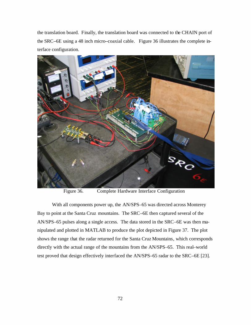
72
the translation board. Finally, the translation board was connected to the CHAIN port of
the SRC–6E using a 48 inch micro–coaxial cable. Figure 36 illustrates the complete in-
terface configuration.
Figure 36. Complete Hardware Interface Configuration
With all components power up, the AN/SPS–65 was directed across Monterey
Bay to point at the Santa Cruz mountains. The SRC–6E then captured several of the
AN/SPS–65 pulses along a single access. The data stored in the SRC–6E was then ma-
nipulated and plotted in MATLAB to produce the plot depicted in Figure 37. The plot
shows the range that the radar returned for the Santa Cruz Mountains, which corresponds
directly with the actual range of the mountains from the AN/SPS–65. This real–world
test proved that design effectively interfaced the AN/SPS–65 radar to the SRC–6E [23].

73
5 10 15 20 25 30 35 40 450
1
2
3
4
5
6
7
8
9
10
x 104
Range (km)
Pro
cess
ed R
adar
Ret
urn
AN/SPS-65 Radar Return via SRC-6E processor
Σ I Channel SignalΣ PRF
Figure 37. Reconstructed Radar Data Collected by the SRC–6E (From Ref. 23.)
D. CHAPTER SUMMARY
This real–world testing proved that the hardware interface design effectively al-
lowed the SRC–6E to interface with a high–speed data source and effectively process the
data. Time constraints permitted testing only the I channel and PRF timing reference
signals from the AN/SPS–65. However, enough data was captured to perform basic
range analysis on a known target which was the overall goal of the design.

74
THIS PAGE INTENTIONALLY LEFT BLANK

75
VIII. CONCLUSIONS
A. DESIGN SUMMARY
The entire purpose of the hardware interface design was to interface the SRC–6E
reconfigurable computer at the Naval Postgraduate School to a high–speed data source.
To prove the real–world applicability of such an interface, the AN/SPS–65 radar was se-
lected as the data source. The goal of the hardware interface design was to implement,
develop, and test the requisite hardware needed to permit the SRC–6E to process the data
received by the AN/SP–65 to calculate the range of a target.
The data received by the AN/SPS–65 is carried on the ± 5.8–V I and Q channels
while the internal amplification value of these two channels is carried on the separate 0–
12 V AGC voltage signal. The AN/SPS–65 also produced a 0 to 1.0–V pulse repetition
frequency signal to generate a timing reference for the received RF signals. The signals
were connected to a custom–built analog board which buffered each signal and either
amplified or attenuated the signal for proper compatibility with other parts of the design.
The I, Q, and AGC voltage signals were attenuated to ± 225 mV to be compatible with
the MAX108 ADC analog inputs and the PRF timing reference signal was amplified to
LVTTL to be compatible with the SRC–6E.
The I, Q, and AGC voltage signals were connected to individual MAX108-
EVKITs where they were sampled at 100 MHz by the MAX108 ADCs. The LVPECL
outputs of each MAX108EVKIT were routed via shielded controlled impedance cables to
a custom built translation board. On the translation board, the LVPECL signals were
translated to LVTTL and routed, along with the PRF timing reference signal from the
analog board, to a 114–pin MICTOR connector. Micro–coaxial cable was then used to
connect the MICTOR connector of the translation board to the MICTOR connector of the
CHAIN port on the SRC–6E, completing the interface between the radar and the SRC–
6E. The translation board also took the 100–MHz sample clock generated by the SRC–
6E from the MICTOR connector and translated it into a differential ECL clock. This dif-
ferential ECL clock was then routed through a clock driver for distribution to the three
MAX108EVKITs.

76
B. DESIGN ACCOMPLISHMENT
The complete interface testing conducted in Chapter VII proved that the SRC–6E
and the hardware interface were fully capable of interfacing to the AN/SPS–65 radar.
Though time constraints only allowed for complete interface testing of the I channel, the
use of the I channel provides enough information to calculate the range of a target. The
Q channel is identical to the I channel except for a 90 degree phase shift induced to
eliminate the possibility of “phase blindness” [8]. Also, the AGC voltage is not required
for processing the I or Q channel. Therefore, limiting the testing to the I channel does not
detract from the ability of the interface to bring data from an external high–speed device
into the SRC–6E through its CHAIN port.
The initial design goal was to drive the MAX108EVKITs with a 200–MHz sam-
ple clock and to utilize the MAX108 demultiplexing feature to reduce the output data rate
to the 100–MHz system bus speed of the SRC–6E. The initial testing of the I channel on
the lab bench and in the complete interface configuration proved that the interface design
was capable of implementing this configuration. However, it was discovered that they
was no way to ensure that the I channel and Q channel samples were in phase with each
other. This was due to the random phase relationship between the sample clock and
DREADY on startup in DIV2 mode. Since no reset signal path was incorporated in the
translation board design, there was no method to use the RSTIN inputs on the MAX108-
EVKIT to synchronize all three MAX108EVKITs. To avoid redesigning the translation
board, it was decided to place the MAX108EVKITs in DIV1 mode and to use a 100–
MHz sample clock. This would ensure that all three MAX108EVKITs outputs remained
in–phase and still allowed the design to sample over 1.5 times the Nyquist frequency of
60 MHz. Though the sampling rate was cut in half, the 100–MHz sampling rate provided
more than enough resolution to effectively process the data coming from the AN/SPS–65.
The design met the established goal of interfacing the AN/SPS–65 radar to the
SRC–6E reconfigurable computer. The design tested focused only on the SDR mode of
the SRC–6E, but engineered all aspects of the design to be capable of exploiting the DDR
capability of the SRC–6E allowing room for future speed–ups. To provide flexibility of
implementation, the bandwidth of the analog board and the MAX108EVKITs allows the
design to be capable of interfacing with other radars with similar output signals to the

77
AN/SPS–65. Ultimately, the designed proved that the CHAIN port of the SRC–6E is a
very capable high–speed port that can be effectively interfaced with external devices
through user–defined hardware.
C. RECOMMENDATIONS FOR FUTURE WORK
The design only utilized the SDR mode of the SRC–6E, which limited the data
rate into the CHAIN port to a maximum of 100 MHz. Using the DDR mode of the SRC–
6E in the final design configuration with the MAX108s set in DIV1 mode would allow
the input signals to be sampled at 200 MHz. Combining the DDR mode with a RSTIN
capability on the translation board would allow the use of the DIV2 mode of the
MAX108 and would increase the maximum sampling rate to 400 MHz. This would pro-
vide for greater resolution of sampled signals as well as allow the SRC-6E to sample sig-
nal sources with frequenc ies in excess of its 100–MHz system bus.
The final form of the design used five different printed circuit boards of devices
between the analog board, three MAX108EVKITs, and the translation board. If more
robust PCB CAD software was used, all five boards could be consolidated onto one.
This would reduce the amount of cabling required for power and signal transmission.
Signal transmission would also be greatly improved due to shorter transmission lengths
between devices and the ability to match transmission line impedances. In addition, the
number of power supplies required for the interface could be reduced if onboard voltage
regulators were implemented to generate the requisite termination voltages.
The CHAIN port interface of future SRC designs would benefit greatly from al-
lowing the user to implement any of the input and output signal levels supported by
Virtex-II FPGAs. This would increase the overall flexibility of the CHAIN port by al-
lowing it to directly interface to a broader range of hardware without the need for costly
and potentially bandwidth limiting translator chips. If the input and output signal settings
need to be configured at the factory, the user should have the option to choose the logic
level implemented. If production constraints limit the logic level setting to only one in-
put and output logic standard, then either (LV)ECL or (LV)PECL should be implemented
instead of LVTTL. More and more modern data and signal processing devices are re-

78
quiring data rates in the gigahertz range. To effectively process and transmit these sig-
nals, the overall propagation delay needs to be reduced while simultaneously reducing the
effect of noise on the signal itself. The logic families of (LV)ECL and (LV)PECL in dif-
ferential format offer propagation delays under 500 ps and are very noise resistant [24].
In addition to being able to set the logic levels to (LV)ECL or (LV)PECL, removable or
selectable termination resistors on the CHAIN port signal lines would simplify the inter-
face implementation. By making the CHAIN port compatible with these logic levels, the
SRC–6E would be even more useful for real–time high–speed signal processing pur-
poses.

79
APPENDIX A CHAIN PORT PIN LISTING (AFTER REFS. 6 & 7.)
This appendix provides a listing of the CHAIN port pins, the corresponding
Vitrex–II pins, the Virtex–II pin description, and the bank the pin is located in.
Port A Chain Port Pin Virtex-II
Pin Virtex-II Pin Descrip-
tion Bank
Number Notes
IN.1 U12 IO_L53P_2 2 IN.2 T12 IO_L53N_2 2 IN.3 M2 IO_L52P_2 2 IN.4 N2 IO_L52N_2 2 IN.5 R11 IO_L51P_2 2 IN.6 T11 IO_L51N_2 2 IN.7 P8 IO_L50P_2 2 IN.8 N8 IO_L50N_2 2 IN.9 M3 IO_L49P_2 2 IN.10 N3 IO_L49N_2 2 IN.11 M5 IO_L48P_2 2 IN.12 N5 IO_L48N_2 2 IN.13 R10 IO_L47P_2 2 IN.14 P10 IO_L47N_2 2 IN.15 K1 IO_L46P_2 2 IN.16 L1 IO_L46N_2 2 IN.17 L4 IO_L45P_2 2 IN.18 M4 IO_L45N_2 2 IN.19 P9 IO_L44P_2 2 IN.20 N9 IO_L44N_2 2 IN.21 L3 IO_L43N_2 2 IN.22 L6 IO_L36P_2 2 IN.23 M6 IO_L36N_2 2 IN.24 R12 IO_L35P_2 2 IN.25 P12 IO_L35N_2 2 IN.26 J2 IO_L34P_2 2 IN.27 K2 IO_L34N_2 2 IN.28 J4 IO_L33P_2 2 IN.29 K4 IO_L33N_2 2 IN.30 M8 IO_L32P_2 2 IN.31 L8 IO_L32N_2 2 IN.32 H1 IO_L31P_2 2 IN.33 J1 IO_L31N_2 2 IN.34 L7 IO_L30P_2 2 IN.35 M7 IO_L30N_2 2 IN.36 P11 IO_L29P_2 2 IN.37 (Valid) N11 IO_L29N_2 2 IN.38 (Full) D1 IO_L21P_2 2 IN.39 (Clock) F19 IO_L96N_1/GCLK3P 1
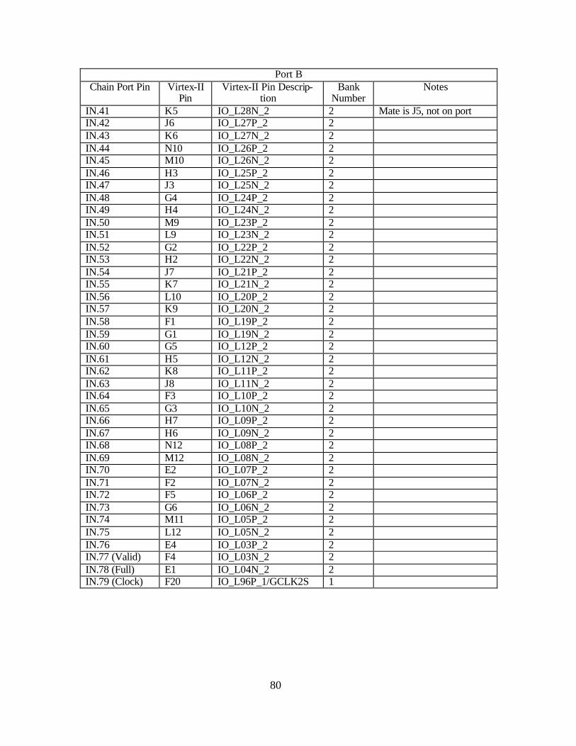
80
Port B Chain Port Pin Virtex-II
Pin Virtex-II Pin Descrip-
tion Bank
Number Notes
IN.41 K5 IO_L28N_2 2 Mate is J5, not on port IN.42 J6 IO_L27P_2 2 IN.43 K6 IO_L27N_2 2 IN.44 N10 IO_L26P_2 2 IN.45 M10 IO_L26N_2 2 IN.46 H3 IO_L25P_2 2 IN.47 J3 IO_L25N_2 2 IN.48 G4 IO_L24P_2 2 IN.49 H4 IO_L24N_2 2 IN.50 M9 IO_L23P_2 2 IN.51 L9 IO_L23N_2 2 IN.52 G2 IO_L22P_2 2 IN.53 H2 IO_L22N_2 2 IN.54 J7 IO_L21P_2 2 IN.55 K7 IO_L21N_2 2 IN.56 L10 IO_L20P_2 2 IN.57 K9 IO_L20N_2 2 IN.58 F1 IO_L19P_2 2 IN.59 G1 IO_L19N_2 2 IN.60 G5 IO_L12P_2 2 IN.61 H5 IO_L12N_2 2 IN.62 K8 IO_L11P_2 2 IN.63 J8 IO_L11N_2 2 IN.64 F3 IO_L10P_2 2 IN.65 G3 IO_L10N_2 2 IN.66 H7 IO_L09P_2 2 IN.67 H6 IO_L09N_2 2 IN.68 N12 IO_L08P_2 2 IN.69 M12 IO_L08N_2 2 IN.70 E2 IO_L07P_2 2 IN.71 F2 IO_L07N_2 2 IN.72 F5 IO_L06P_2 2 IN.73 G6 IO_L06N_2 2 IN.74 M11 IO_L05P_2 2 IN.75 L12 IO_L05N_2 2 IN.76 E4 IO_L03P_2 2 IN.77 (Valid) F4 IO_L03N_2 2 IN.78 (Full) E1 IO_L04N_2 2 IN.79 (Clock) F20 IO_L96P_1/GCLK2S 1

81
Port C Chain Port Pin Virtex-II
Pin Virtex-II Pin Descrip-
tion Bank
Number Notes
IN.81 D2 IO_L01P_2 2 IN.82 E3 IO_L01N_2 2 IN.83 B4 IO_L01P_1 1 IN.84 C4 IO_L01N_1 1 IN.85 C6 IO_L04P_1 1 IN.86 C5 IO_L04N_1 1 IN.87 E8 IO_L06P_1 1 IN.88 F8 IO_L06N_1 1 IN.89 A5 IO_L07P_1 1 IN.90 A4 IO_L07N_1 1 IN.91 B6 IO_L10P_1 1 IN.92 B5 IO_L10N_1 1 IN.93 H11 IO_L11P_1 1 IN.94 H12 IO_L11N_1 1 IN.95 C8 IO_L19P_1 1 IN.96 C7 IO_L19N_1 1 IN.97 E7 IO_L20P_1 1 IN.98 D8 IO_L20N_1 1 IN.99 E10 IO_L21P_1 1 IN.100 E9 IO_L21N_1 1
Port D Chain Port Pin Virtex-II
Pin Virtex-II Pin Descrip-
tion Bank
Number Notes
IN.103 J10 IO_L02P_1 1 IN.104 H10 IO_L02N_1 1 IN.105 J11 IO_L05N_1 1 IN.106 G10 IO_L09P_1 1 IN.107 G9 IO_L09N_1 1 IN.108 F9 IO_L12N_1 1

82
THIS PAGE INTENTIONALLY LEFT BLANK

83
APPENDIX B SRC–6E PART NUMBERS
This appendix lists the specific part numbers of the devices used by SRC Com-
puters, Inc. in the SRC–6E.
A. USER LOGIC FPGAS [6]
Description: Xilinix Virtex-II
Part Number: XC2V6000–4FF1517C
B. MICRO–COAXIAL CABLE [6]
Description: Cable, AMP, 47” 50 −Ω 114 Pos. Straight/Straight
SRC Part Number: 2500–0007
Manufacturer Part Number:
0138501141119JM20
Manufacturer Precision Interconnect
C. 114–PIN AMP MICTOR CONNECTOR [6]
Description: Connector, MICTOR 114 Pin
SRC Part Number: 0400–0018
Manufacturer Part Number:
767054-3
Manufacturer AMP

84
THIS PAGE INTENTIONALLY LEFT BLANK

85
APPENDIX C LOGIC ANALYZER DATA
This appendix provides a listing of the data captured by the HP16500B logic ana-
lyzer from the MAX108EVKIT testing.
Label > CLK PRI AUX __________ ___ ___ ___ Base > Hex Hex Hex 0 1 100 103 1 1 094 097 2 1 090 093 3 1 086 088 4 1 081 084 5 1 079 081 6 1 077 078 7 1 075 076 8 1 074 074 9 1 074 074 10 1 074 074 11 1 076 075 12 1 078 076 13 1 080 079 14 1 084 082 15 1 087 085 16 1 092 090 17 1 098 095 18 1 103 100 19 1 109 106 20 1 115 112 21 1 121 118 22 1 127 124 23 1 133 130 24 1 139 136 25 1 145 142 26 1 151 148 27 1 156 153 28 1 160 158 29 1 164 162 30 1 168 166 31 1 170 169 32 1 172 171 33 1 173 172 34 1 174 173 35 1 173 174

86
36 1 172 172 37 1 170 172 38 1 168 170 39 1 166 167 40 1 163 164 41 1 157 159 42 1 152 155 43 1 148 150 44 1 142 146 45 1 136 139 46 1 131 134 47 1 124 127 48 1 119 121 49 1 113 115 50 1 107 109 51 1 101 104 52 1 095 098 53 1 090 093 54 1 086 090 55 1 082 085 56 1 079 081 57 1 078 079 58 1 075 076 59 1 075 074 60 1 074 074 61 1 074 074 62 1 075 074 63 1 077 076 64 1 079 078 65 1 082 081 66 1 086 084 67 1 091 089 68 1 096 093 69 1 101 099 70 1 107 104 71 1 113 110 72 1 119 116 73 1 126 122 74 1 132 129 75 1 138 135 76 1 143 140 77 1 149 147 78 1 154 152 79 1 159 157 80 1 163 161 81 1 167 165

87
82 1 169 168 83 1 171 170 84 1 172 172 85 1 174 173 86 1 173 174 87 1 172 173 88 1 171 173 89 1 169 170 90 1 167 167 91 1 163 164 92 1 158 162 93 1 154 157 94 1 149 152 95 1 144 146 96 1 139 142 97 1 132 135 98 1 126 130 99 1 121 123 100 1 114 117 101 1 109 111 102 1 103 105 103 1 097 100 104 1 093 094 105 1 088 090 106 1 083 086 107 1 081 082 108 1 077 079 109 1 076 077 110 1 075 075 111 1 074 073 112 1 074 074 113 1 075 075 114 1 076 076 115 1 079 077 116 1 082 080 117 1 085 083 118 1 090 087 119 1 095 092 120 1 100 097 121 1 106 102 122 1 111 108 123 1 117 114 124 1 124 120 125 1 130 127 126 1 136 133 127 1 142 139

88
128 1 147 144 129 1 153 150 130 1 157 155 131 1 162 160 132 1 165 164 133 1 169 167 134 1 170 169 135 1 172 172 136 1 173 173 137 1 173 173 138 1 173 173 139 1 172 172 140 1 170 171 141 1 167 169 142 1 164 166 143 1 161 162 144 1 156 158 145 1 151 153 146 1 145 148 147 1 140 143 148 1 135 137 149 1 128 131 150 1 122 124 151 1 115 120 152 1 110 113 153 1 105 108 154 1 099 102 155 1 095 096 156 1 090 092 157 1 085 087 158 1 081 083 159 1 078 079 160 1 076 077 161 1 074 076 162 1 074 074 163 1 073 074 164 1 075 075 165 1 075 075 166 1 078 077 167 1 081 079 168 1 084 082 169 1 089 086 170 1 093 091 171 1 098 095 172 1 104 101 173 1 109 107

89
174 1 116 112 175 1 122 118 176 1 128 125 177 1 134 131 178 1 140 137 179 1 146 143 180 1 151 149 181 1 156 154 182 1 161 159 183 1 165 163 184 1 168 167 185 1 170 169 186 1 172 171 187 1 173 172 188 1 174 173 189 1 173 173 190 1 172 173 191 1 171 171 192 1 168 169 193 1 164 166 194 1 162 163 195 1 157 159 196 1 152 155 197 1 148 150 198 1 142 145 199 1 136 138 200 1 129 132 201 1 123 126 202 1 118 120 203 1 111 114 204 1 105 108 205 1 100 103 206 1 096 098 207 1 090 093 208 1 086 088 209 1 082 084 210 1 079 081 211 1 076 078 212 1 076 075 213 1 074 075 214 1 074 074 215 1 074 074 216 1 075 075 217 1 077 076 218 1 079 078 219 1 083 081
90
220 1 087 085 221 1 092 089 222 1 097 094 223 1 102 099 224 1 108 105 225 1 114 111 226 1 120 117 227 1 126 123 228 1 132 129 229 1 138 135 230 1 144 141 231 1 150 147 232 1 155 152 233 1 159 157 234 1 163 162 235 1 167 165 236 1 170 169 237 1 172 171 238 1 173 172 239 1 173 173 240 1 173 173 241 1 172 172 242 1 171 172 243 1 168 170 244 1 166 167 245 1 163 164 246 1 158 160 247 1 153 156 248 1 149 151 249 1 143 146 250 1 138 141 251 1 131 134 252 1 125 128 253 1 119 122 254 1 113 116 255 1 107 110 256 1 102 104 257 1 097 099 258 1 092 095 259 1 088 090 260 1 083 085 261 1 081 081 262 1 078 078 263 1 076 077 264 1 075 074 265 1 074 074

91
266 1 074 074 267 1 075 074 268 1 077 076 269 1 079 078 270 1 082 081 271 1 086 084 272 1 090 088 273 1 095 093 274 1 100 098 275 1 106 103 276 1 112 109 277 1 118 115 278 1 124 121 279 1 131 127 280 1 137 134 281 1 143 140 282 1 148 145 283 1 153 150 284 1 158 156 285 1 163 160 286 1 166 164 287 1 168 167 288 1 171 170 289 1 173 172 290 1 173 173 291 1 173 174 292 1 172 173 293 1 172 173 294 1 169 171 295 1 166 169 296 1 164 166 297 1 160 162 298 1 154 157 299 1 150 152 300 1 145 148

92
THIS PAGE INTENTIONALLY LEFT BLANK

93
APPENDIX D MATLAB LOGIC ANALYZER PLOTTING SCRIPT
This appendix lists the MATLAB script used to reconstruct and plot the data cap-
tured by the HP16500B logic analyzer.
%testplot.m % %MATLAB script designed to load a test file containing data %captured from a MAX108EVKIT using a HP16500B logic analyzer. %captured data is demultiplexed and needs to be recombined prior %to plotting. %request file to load and number of points to plot fid = input('Enter file name: ','s'); points_to_plot = input('Enter number of points to plot: '); data_array = load(fid); %assign loaded text file a variable name final_array_length = length(data_array)*2; %calculate required array length i=1; for n=1:length(data_array) %loop for number of requested points A(i,1)= data_array(n,4); %store auxiliary port data A(i+1,1)= data_array(n,3); %store primary port data i=i+2; end A = A - 128; %subtract out binary offest A = A * 1.95; %multiply value by 1.95 mV to get voltage value plot(A(1:points_to_plot)); %plot points grid; %display grid

94
THIS PAGE INTENTIONALLY LEFT BLANK

95
APPENDIX E SPICE MODEL OF ATTENUATION CIRCUIT
This appendix list the SPICE model used to simulate the LMH6559 high–speed
buffers.
Test of LMH6559 SPICE Model .include LMH6559.mod * Power Supplies Vcc 1 0 5.0 Vee 2 0 -5.0 * Input Signals *vin 10 0 sin(0.0 .225 200E6) vin 10 0 AC 0.225 * Instance LMH6559 * input, positive power supply, negative power supply, out-put. XBuffer 10 1 2 12 LMH6559 Rload 12 0 50 * Simulation Parameters .tran 2E-8 4E-6 0 .ac lin 300 1E6 500E6 *.TF V(12,0) vin .plot v(12) v(10) .END

96
THIS PAGE INTENTIONALLY LEFT BLANK

97
APPENDIX F SPICE MODEL OF PRF TIMING REFERENCE AMPLIFIER
This appendix lists the SPICE model used to simulate the LMH6643 operational
amplifier.
LMH6643 SPICE Model PRF .include LMH6643.mod * Power Supplies Vcc 1 0 5.0 Vee 2 0 -5.0 * Input Signals vin 10 0 PULSE(0.0 1.0 2ns 1ns 1ns 163.24us 326.48us) * Instance LMH6643 * PINOUT ORDER -IN +IN VCC VEE OUT XOpAmp1 13 11 1 2 12 LMH6643 Rin 0 13 1.2K Rf 13 12 2.7K R1 10 11 820 Rload 12 0 50 * Simulation Parameters .tran 1us 900us 0 .plot v(12) V(10) .END

98
THIS PAGE INTENTIONALLY LEFT BLANK

99
APPENDIX G EXPRESSPCB MANUFACTURING SPECIFICATIONS
The following manufacturing specifications were obtained from the ExpressPCB
website [14].
Manufacturing Specs
> Boards are manufactured with 4 copper layers and plated-through holes.
> Our laminate is FR-4 with an overall thickness of 0.062". The two inner layers have a cop-per weight of 1 ounce. The outer copper layers have a finished copper weight of ~1.25 ounce.
> The final finish of the outer layers is tin-lead reflow.
> The top and bottom solder mask layers are green LPI.
> Pads on the solder mask layers are grown by a minimum of 0.004" on all sides. As a result, very fine pitch surface mount components may not include any solder mask between the pins.
> The board finish is the industry standard of SMOBC.
> The maximum board size we manufacture is 12 x 14 inches.
> The minimum board dimension in height or width is 0.35 inches, however the total board area must be greater than 0.4 square-inches. (i.e. smallest square board we can make is 0.64 x 0.64 inches)
> Etching resolution is: 0.007" minimum trace width, 0.007" minimum space width.
> A white silkscreen is applied to the top side of the board.
> Text placed on a board can be written in copper on the outer layers or drawn in ink on the silkscreen layer. Component outlines will be printed on the silkscreen layer.
> Board perimeters are cut to shape using a 0.093" router bit. Slots in the perimeter must be larger than 0.124". Narrower slots will not be milled correctly. Routing slots or holes in the interior of the board are not offered.
> Sixteen hole sizes are available: 0.008", 0.020", 0.025", 0.029", 0.035", 0.040", 0.046", 0.052", 0.061", 0.067", 0.079", 0.093", 0.110", 0.125", 0.150", 0.192". These sizes are the finished hole diameters after plating. The tolerance for the 0.008" hole is +0.003 / -0.008 (the 0.008" hole may be filled with solder and can only be used as a via). The tolerance for the 0.020" hole is +0.003 / -0.005. The tolerance for the other hole sizes is +/- 0.004". Hole sizes other than those listed are not offered.
> A minimum of 0.021" space must remain between adjacent holes. For example, the center-to-center distance between two pads with 0.020" holes must be 0.041" or greater.
> The dielectric spacing between the top layer and the "Ground" inner layer is 0.012" with a dielectric constant of 4.6 +/-0.2. The dielectric spacing between the bottom layer and the "Power" inner layer is 0.012" with a dielectric constant of 4.6 +/-0.2. The dielectric spacing between the "Power" and "Ground" inner layers is 0.028" with a dielectric constant of 4.7 +/-0.2.
> The two inner layers are solid copper planes. Through-hole pads can either be connected to or isolated from these copper planes. The planes are inset 0.025" from each edge of the board.
> The maximum operating temperature is 125 degrees C.

100
THIS PAGE INTENTIONALLY LEFT BLANK

101
APPENDIX H MICTOR CONNECTOR SCHEMATIC
This appendix illustrate the MICTOR connector schematic used in the translation
board design.

102
THIS PAGE INTENTIONALLY LEFT BLANK
103
LIST OF REFERENCES
[1] David Caliga and David Peter Barker, “Delivering Acceleration: The Potential for Increased HPC Application Performance Using Reconfigurable Logic,” ACM 1–58113–2.093–X/01/0011, November 2001. http://delivery.acm.org/10.1145-/590000/582066/p32-caliga.pdf?key1=582066&key2=9009747011&co-ll=ACM&dl=ACM&CFID=37929187&CFTOKEN=45120840, accessed January 7, 2005.
[2] Andre DeHon and John Wawrzynek, “Reconfigurable Computing: What, Why, and Implications for Design Automation,” ACM 1–58113–109-7/99/06, 1999. http://ieeexplore.ieee.org/iel5/9516/30164/01385107.pdf?tp=&arnumber=1385107&isnumber=30164&arSt=610&ared=615&arAuthor=DeHon%2C+A.%3B++Wawrzynek%2C+J.%3B, accessed January 7, 2005.
[3] Zhi Guo, Walid Najjar, Frank Vahid, and Kees Vissers, “A Quantitative Analysis of the Speedup Factors of FPGAs over Processors,” ACM 1-58113-829-6/04/0002, February 2004. http://delivery.acm.org/10.1145/970000/968304/-p162-guo.pdf?key1=968304&key2=3343287011&coll=ACM&dl=ACM-&CFID=38218966&CFTOKEN=71179759, accessed January 7, 2005.
[4] SRC–6E C Programming Environment v1.2 Guide, SRC–007–04, SRC Com-puters, Inc., Colorado Springs, February 5, 2003.
[5] SRC Computers, Inc., “SRC–6E Training Course,” Training course notes, SRC Computers, Inc., Colorado Springs, 2003 (unpublished).
[6] User Hardware Interfacing to the Chain Port of the SRC MAP® REV D Board, SRC–013–00, SRC Computers, Inc., Colorado Springs, May 19, 2004.
[7] “Virtex-II Platform FPGAs: Complete Data Sheet,” DS031, Xilinx, Inc., San Jose, CA , October 14, 2003. From website: http://direct.xilinx.com/bvdocs/publ-ications/ds031.pdf, accessed January 2, 2004.
[8] Paul D. Buczynski, “AN/SPS–65(V)1 Radar System,” Class material, Naval Postgraduate School, Monterey, July 2002 (unpublished).
[9] “MAXIM MAX108 ±5V, 1.5Gsps, 8-Bit ADC with On-Chip 2.2GHz Track/Hold Amplifier,” 19–1492 (Rev 1), Maxim Integrated Products, Sunnyvale, CA, Octo-ber 2001. From website: http://pdfserv.maxim-ic.com/en/ds/MAX108.pdf, ac-cessed April 1, 2004.
[10] “MAXIM MAX104/MAX106/MAX108 Evaluation Kits,” 19–1503 (Rev 0), Maxim Integrated Products, Sunnyvale, CA, June 1999. From website: http://pdfserv.maxim-ic.com/en/ds/MAX104EVKIT-MAX108EVKIT.pdf, ac-cessed April 1, 2004.

104
[11] William D. Stanely, Operational Amplifiers with Linear Circuits, pp. 501–522, 167-172, Prentice Hall, Upper Saddle River, New Jersey, 2002.
[12] “LMH6559 High–Speed, Closed Loop Buffer,” DS200641, National Semicon-ductor, Santa Clara, California, April 2003. From Website: http://cache.national.c-om/ds/LM/LMH6559.pdf, accessed August 2, 2004.
[13] “LMH6642/6643/6644 Low Power, 130 MHz, 75 mA Rail–to–Rail Output Am-plifiers,” National Semiconductor, Santa Clara, California, April 2004. From Website: http://cache.national.com/ds/LM/LMH6642.pdf, accessed August 2, 2004.
[14] “4–Layer Production Service,” ExpressPCB, Santa Barbara, CA, July 2004. From Website: http://www.expresspcb.com/ExpressPCBHtm/Specs4Layer-Production.htm, accessed August 23, 2004.
[15] Jon Varteresian, Fabricating Printed Circuit Boards, pp. 47–56, Elsevier Science, Woburn, Massachusetts, 2002.
[16] “MC100EPT23 3.3 V Dual Differential LVPECL to LVTTL Translator,” MC100EPT/D (Rev 9), On Semiconductor, Denver, CO, October 2003. From Website: http://www.onsemi.com/pub/Collateral/MC100EPT23-D.PDF, accessed February 9, 2004
[17] “MAXIM MAX9360/MAX9361 LVTTL/TTL/CMOS–to–Differential LVECL/ECL Translators,” 19–2327 (Rev 1). Maxim Integrated Products, Sunny-vale, CA, July 2002. From website: http://pdfserv.maxim-ic.com/en/ds/MAX93-60-MAX9361.pdf, accessed February 6, 2004.
[18] “MAXIM MAX9316A 1:5 Differential (LV)PECL/(LV)ECL/HSTL Clock and Data Driver,” 19–2648 (Rev 0), Maxim Integrated Products, Sunnyvale, CA, Oc-tober, 2002. From website: http://pdfserv.maxim-ic.com/en/ds/MAX9316.pdf, accessed February 6, 2004.
[19] “MICTOR Vertical Connectors for Surface Mount Technology (SMT) Printed Circuit (PC) Board Applications,” (Rev B), Tyco Electronics Corporation, Harris-burg, PA, April 2003. From website: http://ecommas.tycoelectronics.com/com-merce/DocumentDelivery/DDEController?Action=showdoc&DocId=Specification+Or+Standard%7F114-11004%7FB%7Fpdf%7FEnglish%7FS_114-11004_B.pdf, accessed February 3, 2004.
[20] “.100′′ x .100′′ Low Profile Header,” TS–0770–10, 3M Interconnect Solutions Division, Austin, TX, April 2001. From website: http://rocky.digikey.com/Web-Lib/3M/Web%20Data/2500%20Series.pdf, accessed July 19, 2004.
[21] “The ECL Translator Guide,” AN1672/D (Rev 7), On Semiconductor, Denver, CO, November 2002. From website: http://www.onsemi.com/pub/Collatera-l/AN1672-D.PDF, accessed February 17, 2005.

105
[22] “Trace Carrying Capacity Per Mil Std 275,” K & F Electronics, Inc., Fraser, MI. From website: http://www.circuitboards.com/capacity.php3, accessed February 18, 2005.
[23] Thomas. G. Guthrie, Design, Implementation, and Testing of a Software Interface Between the AN/SPS–65(V)1 Radar and the SRC–6E Reconfigurable Computer, Master’s Thesis, Naval Postgraduate School, Monterey, California, March 2004.
[24] John F. Wakerly, Digital Design Principles & Practices, Third Edition, pp. 175-183, Prentice Hall, Upper Saddle River, New Jersey, 2001.

106
THIS PAGE INTENTIONALLY LEFT BLANK

107
INITIAL DISTRIBUTION LIST
1. Defense Technical Information Center Ft. Belvoir, Virginia
2. Dudley Knox Library
Naval Postgraduate School Monterey, California
3. Chairman, Code EC
Department of Electrical and Computer Engineering Naval Postgraduate School Monterey, California
4. Alan Hunsberger
National Security Agency Ft. Meade, Maryland
5. Dr. Russell Duren
Baylor University Engineering Department Rogers, Texas
6. Douglas J. Fouts
Department of Electrical and Computer Engineering Naval Postgraduate School Monterey, California
7. Phillip E. Pace
Department of Electrical and Computer Engineering Naval Postgraduate School Monterey, California
8. Jon Huppenthal
SRC Computers, Inc. Colorado Springs, Colorado
9. David Caliga
SRC Computers, Inc. Colorado Springs, Colorado