naval postgraduate school monterey, … 532 naval postgraduate school monterey, california...
TRANSCRIPT

AD-A275 532
NAVAL POSTGRADUATE SCHOOLMonterey, California
Sn'tiC
:• L::, r-:.S1 0 t994 :
THESIS
COMMUNICATIONS SUBSYSTEM FOR THE PETITEAMATEUR NAVY SATELLITE ( PANSAT)
by
Arnold 0. Brown III
September 1993
Thesis Advisor: Tri T. Ha
Approved for public release; distribution is unlimited.
DnG Q Q1X-C L* S~TD '594-04505
• ,N 31-11

UNCLASSIFiED
"UOUINTY CLASSIPICATMO OF THIS P ASK
REPORT DOCUMENTATION PAGEIa. REPORT SECURITY CLASSIP1CATIO'tJNCLASSIFIED I k. RESTRICTIVE MARKINGS
2. NECURITY CLASSIFICATION AUTHORITY 3. DIGTHIBUTIONIVAILADILITY OF REPORT
2b. ECLASIP QNXINGNONEULEApproved for public release;Zb. ECLUSIICAIONDOWNRAONG CHEULEdistribution is unlimited
4. PERFORMING ORGANIZATION REPORT NUMBER(II) 5. MONITORING6 OIRZANIZATION REPORT RUMBEffRIS
V14WA FRMIG.QW3 IATINIII. OFIC GYDOL7a. NAME OF MONITORING ORGANIZATIONWtial nd omputer Eng Tt4 aPem. Naval Postgraduate School
Naval Postgraduate School ES.a. ADDRESS 1City, Statte, and ZIP Codal 7b. ADDRESS (City. State, and ZIP Codoj
Monterey, CA 93943-5000 Monterey, CA 93943-5000
8a7W NAIOF FUNDINMIPONSORING b.~~ OFFaICESMO 9. PROCUREMENT INSTRUMENT IDENTIFICATION NUMBER
So. ADDRESS (City, State, and ZIP Coda) Q NMNNBRPRORAM PROECT TAK "ORK UNIT N
ELEIMENITIN.NO. NO. ACCESSION
11.* TITLE 11hiehde Sesurity Olaa..Nleatlan)COMMUNICATIONS SUBSYSTEM FOR THE PETITE AMATEUR NAVY SATELLITE ( PANSAT) (U)
14.SUPLZMNTRY OT ' ews expressed inthissthesis are toseof te authcrand donot re et teofficialpolicy or position of the Department of Defense or the United States Government,
17. COUATI CODES I S. SUBEJ CT TERMS (Contlmu. on reverse N na..ueeay and Identify by bleak numb.,'FIEL ROUP *US-ROU COMMUNICATIONS SUBSYSTEM FOR THE PETITE AMATEUR
FED I R U I U . R U N-AVY SATELLITE ( PANSAT)
19. ABSTRACT 10*nibwoan - reverse. IN neeeeeaoy aind Idantify by bNook number)This thesis describes a prototype design for a binary phase shift keyed (BPSK) direct sequence spread spec-trum (DSSS) communications subsystem intended for use in a small lightweight satellite called the PetiteAmateur Navy Satellite (PANSAT). The system was designed using parameters that were established froma link analysis. Included as part of this thesis are the link analysis, schematics, and RF board layouts.
2S. DIDTRIEUTIOWAVAILAEILITY OF ABSTRACT 21M. AE*TRACT SECURITY CLAUSSWICATION[I UNCLASSIFIED/UNUMITNEE SAME AS RPT. [] DYIC USER, UNCLASSIFIED
O, ri1aNIL INIIDA I8jhI ol6(e Area oa a YBODD FORM 1473, 64 MAR 53 AP Vdta be h used untfl exhaus~ted SECURITY CLASSIFICATION 0FTISPG
All other *dItions are obolt UNCLASSIFIED

Approved for public release; distribution is unlimited
COMMUNICATIONS SUBSYSTEM FOR THE PETITEAMATEUR NAVY SATELLWTE (PANSA T)
byArnold 0. Brown 111
Lieutenant, United States NavyB. S. E. E., San Diego State University, 1987
Submitted in partial fulfillment of therequirements for the degree of
MASTER OF SCIENCE IN ELECTRICAL ENGINEERING
from the
NA\VAL POSTGRADUATE SCHOOLSeptember 1993
Author: & iiArnold 0. Brown II1
Approved by:Tri T. Ha Thesis Advisor
Rudolf Panholzer, Second Read&
Michael A. Morgan, ChauiKian,Department of Electrical and Computer Engineering
ii

ABSTRACT
This thesis describes a prototype design for a binary phase shift keyed (BPSK) direct
sequence spread spectrum (DSSS) communications subsystem intended for use in a small
lightweight satellite called the Petite Amateur Navy Satellite (PANSAT). The system was
designed using parameters that were established from a link analysis. Included as part of
this thesis are the link analysis, schematics, and RF board layouts.
Accesion For
NTIS CRA&IUTIC l,•AU u:io+• e -
lt I ) Ud)
SA'~it u d Ior
iii

TABLE OF CONTENTS
I. IN TR O D U C TIO N ............................................................................................................... 1
II. LIN K A N A LY SIS ......................................................................................................... 3
III. FUNCTIONAL DESCRIPTION OF THE COMMUNICATIONS SUBSYSTEM ........... 7
A. OVERVIEW OF THE COMMUNICATIONS SUBSYSTEM ......................... 8
B. BOARD 1: TRANSMITTER AND RECEIVER FRONT END ...................... 10
C. BOARD 2: RECEIVER IF AMPLIFICATION, AGC, AND DETECTION ....... 14
D. BOARD 3: RECEIVER TRACKING CIRCUIT .............................................. 18
E. BOARD 4: CARRIER TRACKING LOOP AND DEMODULATOR .......... 21
F. BOARD 5: MODULATION AND AMPLIFICATION .................................. 23
G. BOARD 6: PN GENERATOR AND PHASE SEARCH ............................... 26
IV . CO NCLU SIO N ............................................................................................................ 30
APPENDIX A: PSEUDO NOISE SEQUENCES AND THEIR PROPERTIES .................... 31
A. PSEUDO NOISE SEQUENCES ....................................................................... 31
B. PROPERTIES OF MAXIMAL LENGTH SEQUENCES ............................... 33
APPENDIX B: LINK ANALYSIS PROGRAM AND RESULTS ......................................... 36
APPENDIX C: GENERALIZED IMPEDANCE CONVERTER (GIC) FILTER DESIGN PRO-G R A M ............................................................................................................................................ 46
APPENDIX D: DESCRIPTION OF CIRCUIT SCHEMATICS ........................................... 64
A. BOARD 1: TRANSMITTER AND RECEIVER FRONT END ..................... 64
B. BOARD 2: RECEIVER IF AMPLIFICATION, AGC, AND DETECTOR ........ 66
C. BOARD 3: PN SEQUENCE TRACKING ...................................................... 70
D. BOARD 4: CARRIER TRACKING LOOP AND DEMODULATOR .......... 71
E. BOARD 5: PN PHASE MODULATION AND AMPLIFICATION .............. 73
F. BOARD 6: PN GENERATION AND PHASE SEARCH CIRCUITS ........... 75
LIST O F REFERENC ES ........................................................................................................... 93
INITIAL DISTRIBUTION LIST ............................................................................................ 94
iv

I. INTRODUCTION
The goal of this project is, to develop a direct sequence spread spectrum binary phase
shift keyed (BPSK) communiications subsystem for the Petite Amateur Navy Satellite
(PANSAT). Previous work on this topic primarily focused on modulator and demodulator
(MODEM) designs that utilized various modulation techniques, such as BPSK, and four
frequency shift keying (4,.FSK). These MODEMs were designed to operate at 1200 bps,
have a pseudo noise sequence length of 127, and have a chip rate (fchip) of 152.4 kHz.
With a chip rate of 152.4 kHz, the null to null bandwidth of the transmitted signal was only
2fellr - 304.8 kHz. The link analysis, which determined these and other parameters such as
a required transmitter power of 7 watts, was found to be in error. Fortunately, the
conservative link analysis that is included as part of this thesis provides communication
system performance parameters that far exceed those previously discussed. However, the
new parameters called for more bandwidth than was previously understood to be available
from the Federal Communications Commission (FCC) and the American Radio Relay
League (ARRL). As it turned out, the project only requested 1 MHz of bandwidth, and that
is all the ARRL awarded, 1 MHz of bandwidth centered at 437.25 MHz. After a review of
all documentation and applicable rules manuals, this too was found to be in error. The
rules actually allow space operations anywhere from 435-438 MHz. So to accommodate
the wider band signal the center frequency was moved to 436.5 MHz.
Part of the problem was that the communications system was not being looked at, or
designed as a system. Previous efforts, in addition to being based on faulty data, ignored
the rest of the communications problem by concentrating solely on the MODEM designs.
Following the discovery of the errors previously mentioned, it was recognized that the
communications problem needed to be approached as a system. So this thesis project was
expanded from the design of a MODEM to the design of a complete communications

subsystem. The intent was not only to design, but to design, build, and test the complete
communications subsystem.
This thesis begins with an explanation and results of the most recent link analysis.
Followed by a functional description of the communications subsystem that evolved
during the course of this thesis work. The details of this work, such as the schematics and
board layouts have been included as appendices. Additional information on pseudo noise
sequences, the link analysis, and filter design may also be found in the appendix.
2

II. LINK ANALYSIS
Before attempting a design of either the transmitter or receiver, a link analysis was
performed for both the up-link and down-link. Past experience has shown that even though
the link budget equation is very simple, minor errors are easily made. That is why a general
link analysis program was written using MATLAB® and included as Appendix B. Most
of the equations used in the program came from [Ref. l:p. 390-396]. Some of these
equations are repeated here for clarity. This Matlab® program allows the user to quickly
vary the system parameters and plot the results over a wide range of transmitter power. The
results are output in both graphical and tabular formats. The tabular format provides,
among other things, an estimate of the received carrier power at the base of the antenna.
This estimate is then used to compute the power throughout the design.
As one might expect, the receiver will have to process a very weak signal; just how
weak is what needed to be determined. The answer was provided by the link analysis
program. A main concern was that the noise added by the receiver components might
obscure this weak signal. Fortunately, the receiver's noise figure may be controlled though
the proper selection of receiver components such as the low noise amplifier (LNA). Once
the receivers noise figure is known, the carrier-to-noise-ratio may be computed. Because
each amplifier stage amplifies the signal and noise equally, the carrier to noise ratio at the
front of the receiver is the same as the carrier to noise ratio at the detector.
(~D (~DX =(2.1)
Since this ratio remains constant throughout the receiver, the noise power may be ignored
and the signal power used exclusively in power calculations.
3

Parameters Values
Gain of Amplifier Stages G = 22.5, 27, 27, 27 dB
Noise Figures of Amplifier Stages NF - 2, 1.6, 1.6, 1.6 dB
Eath Station Antenna Gain Groanh = 12 dB
Satellite Antenna Gain GSatellite = 0 dB
Antenna Noise Temperature TA = 280* Kelvin
Antenna Elevation Angle E = 50
Transmitter Carrier Frequency f, 436.5 MHz
Earths Radius R 6378.153 kr
Altitude of the Satellite h = 480 kin
Speed of light c m 2.997925 X10⁵ (m/s)
Botzznan's Constant k - !.38xiO" 3
'hble 241: System parameters used in the link analysis.
For the purpose of comparison, the transmitter power was varied from 0.2 watts to 2.0
watts and the resulting effective isotropic radiated power (PIIRP) computed using the
following equation.
PEIRP = PtGt (2.2)
Parameters such as P, and G, are shown in Table 2-1. Once the PEIRP is known the
received carrier power may be computed using equations (2.3) and (2.4). Equation (2.4) is
used to determine the amount of loss due to free space.
CRx (PEIRP) +GAR - LFS (2.3)
(LFS)da = 20log [ (4d-)] (2.4)
The noise component of is computed using equations (2.5) through (2.8). These
TNsct
equations are used to compute the system noise temperature. Lookir.g at equation (2.8) it
is easy to see why the low noise amplifier (LNA) is the single largest
4

contributor to the receivers noise figure and noise temperature and why its selection in
terms of gain and noise figure is so important.
NRX =kT, YBIF (2.5)
T, 5 t =TAR +TC (2.6)
Te = T.(F. - 1) (2.7)
•:F I F2 F nFe= FLN + 0 + + + (2.8)
SLNA GLNAGI GLNAGI...Gn
Since this link analysis considers only the worst case, the slant range (d) was onlyu
computed for an elevation angle of E = 5 using the following equation.
d = 4 (R+h)2+R2-2R(R+h)sin E7-r+asin ( RI ) sE (2.9)
The results are then converted to dB's, thus reducing the problem to simple addition.
(PEIRP) dfw = IOIog(PEIRP) (2.10)
kdD = lOlog (1.38x10- 23) = - 2 2 8 .6 dB (2.11)
BdB = 101og(BI) (2.12)
(N) = E1P~DW (LFdB (TAR) -kda,- BdB (2.13%))d (PEIRP)d ,I~ -- FS) di + -- kdi ld
dB SYat dD
(NI) =-(C)d+B-Rd (2.14)
Now that --b is known, the probability of a bit error may be calculated using the errorN.
correction function as shown in the following equation.
b= '(Ie-erft W (2.15)
5L

A graph of the bit energy-to-noise-ratio as a function of the information bit rate and
transmission power i., shown below.
BiDo Eziay to Noir RAtiowva fWom im Bit Rrde35 T
20 .... .... ... . , . ... , 1 .- - , .
I L'
S 1
10 ........... ........ .. .. . . .
0 2 0 0 40 o0 l0o 0 p oot 1000 o 120 WoLnorvmano Bit Rate fts)
Figure 2-1 Bit energy to noise ratio vs. the informationbit rate over a power range from 0.2 to 2.0 watts. Thelowest curve is for 0.2 watts.
Graphs showing the probability of error are not included here, because the probability of
error is so low, but may be found in Appendix B. Appendix B also contains the
MATLAB® program and a set of tabular results for the data in Table 2-1.
6

HIl. FUNCTIONAL DESCRIPTION OF THE COMMUNICATIONS
SUBSYSTEM
The following discussion is conducted using simplified block diagrams of actual
boards designed duri'g the course of this thesis work. Following a brief explanation of the
ovei:all system, each board will be discussed individually. If more detail is desired, it may
be found in the schematics and layout diagrams included in Appendix D. If the reader
requires a review of spread spectrum communications or wishes to see mathematical proofs
of concepts applied here, References 5, 7, and 11 are suggested.
Equations used here may be written differently than those found in most text books.
In most commnunications text books a signal is described mathematically as
S(t) = 22Pcos(o),t+0(t-t) -*) (3.1)
where F2P is the power of the signal, 0 (t - c) is the phase modulation with 'C representing
a phase shift due to the channel, and 0 is the carrier phase shift due to the channel. Since
this thesis is a practical application of communications theory and mathematics, signals
will be described in the following way
S (t) = PdDNIcOS ((•t + 0 (t-'t) - ) (3.2)
It seems more practical to write signal equations in this manner, because component
catalogs express gain, loss, and power in units of dBs and dBms. Now gains and losses
may be accounted for with simple addition and subtraction.
S(t) = (Pd11,,+GdD-LIL) COS (Cct + 0 (t -r)-q) (3.3)
With signal povwer expressed in this way, the reader may easily apply these equations to
the circuits in Appendix D, and use a spectrum analyzer to measure signal levels at critical
points in the design. Measurements may be made by simply tuning to the carrier
WI)frequency r- = , adjusting the span to Z 2(data rate), and moving the marker to the peak
of the signal waveform, which in this case is a SINC2 function.
7

A. OVERVIEW OF THE COMMUNICATIONS SUBSYSTEM
Every spread spectrum communications system must perform &.e same basic
functions. The transmitter must spread the data spectrally, up-convert to the carrier
frequency, amplify the signal and radiate it from an antenna. Every spread spectrum
receiver must down-convert from the carrier frequency, provide doppler compensation if
necessary, amplify the received signals, detect the desired signal, track it, de-spread it, and
demodulate it. What could be simpler? Well, the devil is in the details.
This communications subsystem affords the user flexibility by providing the ability
to:
o Select between redundant transmitters and receivers
* Select a desired transmitter power from a range of power levels
• Evaluate numerous PN phase search strategies, and use the one that provides thequickest acquisition time possible
• Switch between straight BPSK and spread spectrum BPSK
* Compensate for doppler shift using the ground station only
• Develop and test a faster acquisition circuit in the future
Starting with a link analysis this communications subsystem was designed as a system.
The design is modular, with each board performing a different and unique function.
Circuit design and component selection was based on power levels that were determined
from the link analysis and used io calculate the signal power throughout the design.
Because of the interdependency on signal power levels between each board, an iterative
approach to the design was employed. The design evolved, as the designer became more
aware of the practical aspects of circuit design and component selection.

II
Oi-i| I
u
21 1&CA
Mal iip
449

Figure 3-1 is a functional diagram of the present design, where:
"• Board 1: provides up-conversion, down-conversion, and amplification.
"* Board 2: provides receiver IF amplification, automatic gain control (AGC), andcoarse PN phase detection.
"* Board 3: provides fine PN phase alignment and tracking.
"* Board 4: de-spreads the signal, locks on to the phase of the suppressed carrier, anddemodulates the data.
"* Board 5: provides modulation and amplification of PN sequences developed onboard 6 and applied to boards 2-4.
"* Board 6: provides PN phase generation, search, and control logic, as well as any otherdigital circuitry used in the design.
Though not yet complete, this design makes significant strides in the right direction. With
its flexibility and modularity, the opportunity is there for future designers to continue its
evolution or use it as a test bed for new and improved designs.
B. BOARD 1: TRANSMITTER AND RECEIVER FRONT END
Board 1 groups all the components with SMA connectors together. Connections via
SMA and 50L- cable eliminate printed circuit board (PCB) design problems that would
likely occur at frequencies above the first IF frequency of 32.1 MHz. Board 1 is designed
to serve in either the satellite, using a fixed 404.4 MHz oscillator or in the ground station,
using a variable 404.4 MHz oscillator. The variable oscillator's control input will come
from a program called the Kansas City Tracker that predicts the orbital track of the satellite.
This method of doppler compensation eliminates the need for tunable filters in the satellite
and places the burden of doppler compensation solely on the ground station. Another more
obvious way to achieve doppler comi.•asation is to simply widen the filter bandwidths.
This method was ruled out because th- maximum doppler shift is projected to be ± 10 kHz,
while the information bandwidth is 5 20 kHz null to null, making the noise power
bandwidth twice as large as the signal bandwidth.
10
II ~ e I I I ~ l i I[i ili ii lba . . .

111JO
II
I- 1j
11I
hS

The single pjle four throw (SP4T) PIN diode switch allows the user to switch
between two receivers and two transmitters, using two TTL control lines. The cavity
bandpav , filter (BPF) following the SP4T PIN diode switch serves as a preselection filter
for the wideband low noise amplifier (LNA). This preselection filter should eliminate
strong out of band carriers by reducing the noise power bandwidth. The LNA will provide
needed amplification prior to mixing for downconversion to the first IF frequency of 32.1
MHz. The inductor and capacitor (LC) BPF is then used to select the difference frequency
from sum and difference frequencies that result from mixing. The output of the LC BPF is
then feed to the receiver IF strip on board 2.
The upconverter translates the 32.1 MHz IF frequency from board 5 up to the RF
frequency of 436.5 MHz. Here, the BPF following the mixer is used to select the sum of
the local oscillator and IF frequencies. A cavity filter is used because of the high Q and
high center frequency required by the application. The Q is calculated as:
Q f -- 436.5MHz 173 (3.4)
BW 2.52MHz
Unfortunately, the size of these filters is very large when compared to other components.
However, they are passive and have SMA connectors, as do all the components on this
board, so they may be placed anywhere in the satellite.
Because there is still some uncertainty over the amount of power required to complete
Ebthe link with an acceptable -- , an electronic step attenuator was built into the design.
N.
Detrimental channel effects such as multipath fading, are the primary concern. The
electronic step attenuator will allow the controlling ground station to select the most
appropriate transmitter power between 0.2 watts and 2.0 watts. The two amplifiers
following the electronic step attenuator are expected to provide amplification up to a
12

maximum of 2 watts. However, since the project is only in the bread board stage a lower
power amplifier was used.
The received signal will arrive with a random PN sequence phase and random carrier
phase. Each is indicated in the equations that follow, as r for the PN sequence phase and
* for the carrier phase. For simplicity, additive channel noise is neglected.
S,(t) = Pr(dBm) COS [IO)t+0d(t-'-) -J (3.5)
As mentioned above, LOI may be either fixed or variable depending on the application.
Only the fixed oscillator is considered here.
SLOl (t) - (PdBm- 3 dB - LIL) COS (COL0ot) (3.6)
SL1o (t) = PUdfmCOS (COtL0ot) (3.7)
After down-conversion to the first IF frequency, the following is delivered to the receiver
IF strip on board 2.
SA(t) = PA(dBm) C0S[(6O Ic- l)t+Od(t0t) -I] (3.8)
AO(dm) pr(dB) -ILI +GLNA-LC0V - LL2 (3.9)
SA (t) = PA(dBm) l(C0sos1Flt+ed(t-') -$1 (3.10)
The upconverter for the transmitter occupies the bottom half of the board. Its input
comes from board 5.
S(t) = PF(dBm)COS((I0Fit+ed(t)) (3.11)
Naturally, the same local oscillator (LO1) is used for the upconversion to the RF
frequency.
SLOW (t) = P7dDmCOS (0)LO1t) (3.12)
Following upconversion and amplification, the signal delivered to the antenna is
SM(t) = Pt(dBn) cos(wtIt+Od(t)) (3.13)
1) (dBni) PF(dBm) -Lony - LAtin + G 2 1 + G 2 2 (3.14)
13

With only a few minor changes, this design may operate in either spread spectrum
BPSK and straight BPSK. The addition of a PIN diode switch and narrowband filter, in
parallel with the wideband filter following the mixer in the receive path, is necessary to
reduce the noise. power delivered to boards 2 and 4. The PIN diode switch would be used
to select the correct filter, based on the desired mode of operation. Next, the output from
board 6 could be switched high, to lock the bi-phase modulators on board 5 in the zero
phase state. The controller would then only look to boards 2 and 4 for an indication of
detection and lock. On the transmit side, no change to the filter bandwidths is necessary.
Naturally, siice the signal is to rmain nirrowband, the XOR gate on board 6 would be
switched out. So, only boards I n.nd 6 Pare affected by this change in the mode of operation.
C. BOARD 2: RECEIVER 71F AMPLIFICATION, AGC, AND DETECTION
The receiver IF strip and detection circuits were placed on the same board for
convenience bec-iuse they are both relatively small circuits. However, to allow for testing
of a different detection circuit in the future, the two are connected via a 50I cable.
The receiver IF strip provides amplification and automatic gain control (AGC) prior
to distribution to the detection, tracking, and demodulation circuits. An AGC circuit was
built into the design to compensate for anticipated signal fading due to multipath and the
satellite's tumbling. A predetection feedback path was used, as a result of information read
in [Ref. 4 :p. 1624-1628] and the fact that it was easier to build.
14

II iii
I-I I°
'5'
15

The wideband signal coming into the receiver's IF strip may be expressed as
SA(M) - PA(dbm) COS I(0P)t +0d(t-C) -01 (3.15)
and the amplified signal leaving the IF strip as
S 3 (t) = PB (dBm) COS (COlit + 0 (t - T) -- ') (3.16)
where P (d00m) is a result of the gains and losses seen by the signal along the IF strip.
PS(dBm) ' PA(dm) + 02 +G3+G4+G5 +GAC 2 dB - LIL(ALD) - 6 dB - LIL (3.17)
The AGC amplifier used in the circuit and expressed in equation 2.3 provides both
amplification and attenuation over a range of 36 dB [Ref. 6:p. (14-18)]. Naturally, the
amount of gain provided by the AGC amplifier is a function of the voltage output from the
analog level detector. This voltage (VALD) is in millivolts and must be amplified in order
to provide a feedback voltage that varies between zero and five volts.
GAOC = F(VALD06) (3.18)
Once amplified, the signal is distributed to the detection, tracking, and demodulation
circuits via a four-way power splitter.
The detection circuit receives its input from the four way power splitter on the same
board via a 50fl cable to allow for the connection and testing of a different detection circuit
in the future. This circuit is an implementation of a single dwell detector. The concept is
very simple. A search algorithm, implemented using digital components, is used to shift
the phase of the locally generated PN sequence. This locally generated PN sequi.nce is then
bi-phase modulated onto a carrier from L02, amplified, and input to the local oscillator port
of the mixer
SLO2 (t) = P7d~mC0OStiLO 2tL+0(t--t) (3.19)
When the received and locally generated PN sequences come within 1/2 of a chip,
the received signal will be de-spread from wideband to narrowband. The narrowband
BPSK signal will 'pop-up' in the BPF following the mixer. To limit the amount of noise
power bandwidth, the bandwidth of this filter should kept as narrow as possible. Since data
16

ji
is not recovered in the detector, intersymbol interference is not a major concern. In fact,
the bandwidth may be as low as one times data rate, to improve performance in a high noise
environment [Ref. 5:p. 161]. To achieve a narrow bandwidth at the second IF frequency,
a high Q filter was required.
).!^ fe 10.7MHzQM a713 (3.20)
1BW 15kHz
A crystal filter was tie only way to achieve a Q this high. Once de-spread and filtered the
signal may then be detected. The threshold detector receives its signal from the crystal
filter, then provides a TTL signal to board 6, indicating coarse phase alignment.
The autocorrelation of the received and locally generated PN sequences is a stochastic
process. Thus the reason the search algorithm must dwell for a period of time, generally
the code sequence length, before a decision can be made. If c (t) is a PN code sequence
then the autocorrelation of c (t) and a shifted version of itself c (t - -T) may be expressed as
tRe (z) E E(c(t) c (t- -c- E[C21 - (E [c]) 2 a 2- 2var- (mean)2 (3.21)
or
N
R() I R c(t)c(t-,C)dt (3.22)N
2
where the overbar denotes the ensemble average [Ref. 7 :p. 351). The autocorrelation
function may be viewed conceptually, with respect to threshold detector, as a magnitude
scaler to the signal energy in the bandpass filter.
S, (t) - Re (T)pc(dan) COs I (Wp - C0L02) t + em (t - Ol (3.23)
Sr~t M R, (T€) P COS) C.X8 [Ft+ emi(t -'t) -1 (3.24)
IRC0= I when c = eN and Re(,t) N - when * eN (3.25)
N
17

where e is an integer. When the received and locally generated PN sequences come to
within 1/2 of a chip of perfect alignment, the energy delivered to the threshold detector
should be enough to cause a detection (Rc () Pc (dBm)I >threshold). The level of the
threshold may be adjusted by using a variable resistor to change the sensitivity.
D. BOARD 3: RECEIVER TRACKING CIRCUIT
The receiver tracking circuit is an implementation of the non-coherent double dither
loop (DDL) [Ref. 5:p. 188-189]. This scheme utilizes two channels instead of one. The
use of two channels and a subtraction circuit provides the error voltage with a sign (±), thus
indicating the direction of phase change required to increase correlation. Dithering the
early and late PN sequences between the two channels avorage,' out any DC offset or
imbalance inherent in the two channels. The frequency at which they are dithered is
determined by the bandwidth of the BPF's in the arms of the tracking circuit [Ref.5:p. 175].
BWBPP 3.6Dither frequency 4 (3.26)
The error voitage that is produced is then amplified, lowpass filtered, and fed back to the
VCXO of the PN sequence generator on board 6. A window comparator is used to
provide a lock detection signal to board 6.
The wideband signal that is supplied to the tracking circuit board 2 may be expressed
as
S9 (t) = Ps 8 11M)cos (€dl, It + ed (t -'r) - (3.27)
This signal is then amplified before splitting to provide a stronger signal to each channel,
ScG(t) = (Psdan, +G.- 3 d -LIL)cos[tO d(t+-C) -$ (3.28)
St (t) - Pc (d0m) COS l[IFIt + 0d (t- ) - 1 (3.29)
18

ii ii Iii
' - -
I II. 4 4
--- I
iii11
I1

The early and late versions of the estimated PN sequence are then used to bi-phase
modulate the sinewave produced by L02. This signal is then amplified to +7dBm and
applied to the analog switches used to control the dithering. The other side of these
switches is connected to the LO port of the double balanced mixers.
SLO2 (t) = P7dnmCOS [WLO 2t + Oc (t± AT, - ) ] (3.30)
The autocorrelation function may be viewed conceptually, with respect to the analog
level detector, as a magnitude scaler to the signal energy in the bandpass filter.
Sd(t) M (Pe(dBm)-LCohV -LILBpF)Re(,) cos I --wLO 2 )t+0m(t- T)-•1 (3.31)
Sd() "- Pd (dBm) Rc () cos [w1IF2t + Om (t -'C) - 0 (3.32)
The voltage v i produced by the analog level detector is obviously a function of the signal
power applied to it. Its output varies linearly with the input, as shown in [Ref. 6:p. (5-
11)].
V1 = V(IPd(dBm)I) (3.33)
As stated before, the error voltage is produced by subtracting the detector outputs of each
channel.
e (t) = (VI - V2) g (t - nT) (3,34)
This error signal will vary in magnitude at the same frequency as the dither signal
g (t - nT).
Dither frequency = (3.35)Tdifiher
Therefore the cutoff frequency of the loop filter should be much less than the dither
frequency.
20

BWLoop filter (3.36)Tdither
Naturally, this circuit is not used when the communications subsystem is operating in
a straight BPSK mode. Everything may still be allowed to function, but neither the
feedback voltage nor the loop lock detection are used.
E. BOARD 4: CARRIER TRACKING LOOP AND DEMODULATOR
The demodulating circuit is an implementation of a Costas loop [Ref. 7:p. 145] and
[Ref. l:p. 293]. Its input comes from the four-way splitter on board 2.
SB (t) = PB (do m) COS (o 1F It + -d (t -') - (3.37)
Assuming acquisition is successful, the locally generated PN sequence is in phase with the
received PN sequence. So t = c and 0, (t - t) is a punctual version of 0o (t - c).
SL0 (t) = PUdBmCOS (OLO 2t + 0o (t- C)) (3.38)
Since the received signal is being de-spread with a punctual version of the PN sequence,
the autocorrelation function is unity and the signal is maximum.
S. (t) = R, (T) Pv (dBm) COS [ (O)IFI -- OL02) t + 0m (t -- ) (3.39)Pc(d0m) v PlB (dBm) + G10 - Loony - 3dD - LIL (3.40)
Now that the phase of the PN sequences is locked, the BPSK signal must be
demodulated. However, before demodulation can take place, the suppressed carrier must
be tracked. A Costas loop is a phase locked loop designed to lock on to suppressed carrier
signals. Like the tracking circuit, this scheme also utilizes two channels. But, the signals
in these channels are in quadrature.
SIM2 (t) = P.dBmtCOS (WIF2t -) (3.41)
SIF2b(t) = PdBmCOS (IF2t + 2 - (3.42)
21
I2

I'IfB
Lji
L ftt
4.2
22

Since they are in quadrature, the multiplication of the two channels yields their phase
difference, This phase difference is expressed as an error voltage that is amplified, filtered
and fed back to a 10.7 MHz VCXO on board 6.
S, (t) r- (Pc•dm - L..,, + GGic) COS [ (CO1 2 - 0)IF2) t + 0., (t - ) - (3.43)
SQ (t) - (Pccm - l'0NV+ Ooic) cos L (1 F2 - ' 1F2) t + 2 +m (3t44)
Now that the correct phase has been determined for both the locally produced PN
sequence and 10.7 MHz oscillator, the BPSK signal may now be demodulated. Coherent
demodulation is accomplished with an integrate and dump circuit. The integrate and
dump is implemented with an active integrator followed by a sample & hold circuit. The
result is a NRZ signal that may be converted to digital with a comparator. The timing
signal needed to control the integrate and dump is be derived from the PN sequence clock.
This is possible because each data bit is an integer multiple of a PN sequence chip. The
output of the sample & . '.ircuit may then be written as
m(t-C) V eie" I (3.45)d
where • = • and e'• = 1. The NRZ signal m (t - c) is then input into a comparator and
converted to a binary message string m (t - -t) = (0,1).
F. BOARD 5: MODULATION AND AMPLIFICATION
To reduced the number of components on boards 3 and 4 (the tracking and
demodulation circuits), the modulation and amplification circuits of these boards were
placed on a new board named board 5. This board later became the modulation and
amplification board for both the transmitter and receiver.
23

~ j ~jJ s Ii ': ii ii~3a ~ -Ii
2[)- "-
ji1 ii II t _i.
1XjI
IIIII
. 24

The circuit that produces SLO2A and SLO2B will allow testing of a faster acquisition
circuit in the future.
SLo2 (t) -- (P7dm -3 dB -LIL -
3 dB - LIL) COS (CLo2t) (3.46)
SLO2A (t) v (P7dBm -- 3dB -Ll - 3 dB - LIL+ G14 - 3di - LIL) COS (OLO2t) (3.47)
SLo 2B (t) = (P7dBm-3ad-L-LIL- 3 dB-LIL+ GI4- 3 dB-LIL ) cOs (nLo 2t +2 (3.48)
Modulation and amplification of the data to be transmitted, is provided by the circuit
which yields S. (t).
SA (t) (P7dB" - 3 d3 "- LIL -3 dB - LiL+ U12) cos (wOLO2 + ed (t - •)) (3.49)
SA (0 = PA (dam) COS (OLO2t + (t- t)) (3.50)
SD (t) (PA(dBm) - L oony -LIL +G 19 ) Cos [ (OLO2 + (OL3) t + 0d (t) 1 (3.51)
Circuit at the top of the board that produces SL02. and SLo2b, provides an in phase and
quadrature 10.7 MHz sinewave to the Costas loop on board 4.
SLW2U (t) R (P7dDM + G 13 - 3dB - LIL) COS (OLO2t -)
SLO2b () (P7dBm + G3- 3 dB - LIL) COS + - -4) (3.52)2
The circuits in the middle of the board perform basically the same function, bi..phase
modulation of a PN sequence onto a 21.4 MHz carrier (L03), after some amplification and
power splitting.
SB(t) = (PLo2 - 3 do-LIL-Lcohy + G(!1 - 7. 8 dB -LIL) cos ( 2 0ALO2t) (3.53)
SB (t) = PB (dBm) COS (caLO3t) (3.54)
S,(t) ' (PO(dam) -LIL+G, 5 -11 ) Cos (€OLO3tL+0d(t--) (3.55)
SC (0 PC(d~mC) +O (toL0 - (3.56)
25
i'

G. BOARD 6: PN GENERATOR AND PHASE SEARCH
Due to the lack of time, the design of board 6 is incomplete. The intention was to
place all the digital components on one board, thus reducing the number of boards with
digital ground. Digital circuits carry signals that have fast rise times and large voltages,
especially when compared to the weak analog signals of the RF receiver circuits. The
concern is that a noisy digital ground may interfere with the relatively weak analog signals.
1. Transmitter Section
Immediately after the message enters the board it is differentially encoded. This
is done to compensate for phase inversion that may occur during the detection process.
Naturally, the received message stream will have to be differentially decoded following
demodulation in the receiver. The rest of the transmitter circuitry is relatively simple.
Once the fixed PN sequence is produced it is exclusively OR'd with the differentially
encoded message, and the resulting signal is delivered to board 5 for modulation and
transmission. The frequency synthesizer produces timing signals for synchronization of
the sending unit.
2. Receiver PN Synchronization Section
Most of the search strategies read about in References 2 and 5 conduct their search
for the proper PN phase using discrete shifts of the locally produced PN sequence.
Searches such as the one shown in Figure 3-8 may be easily programed, and handled by a
microprocessor. However, concerns over power consumption, and allocation of the on-
board processors resources lead to an implementation that would require little or no
U processor interaction. This part of the design is original, and seeks to Implement the
various search strategies using discrete digital components. A computer is used during the
evaluation phase, in order to make it easier to evaluate different search strategies. Once
evaluated, the search strategy that provides the quickest access time could be implemented
using a state machine to provide the parallel input to the PN sequence generators. If the
state machine is too hard to design, then the satellites on board microprocessor should be
26

iI~ zu
I I) C !."1' --"-II -I= * _ _,
I - I • - -- l}I, '
II IS.... .. I I

able to provide a seed sequence every 813ps without taxing the microprocessors ability to
provide other services. The search strategy shown in Figure 3-8 may be considered a
hybrid of those shown and discussed in [Ref. 9:p. 543]. This strategy might be called a
broken expanding window, since it is combination of the two.
Broken / Expanding-Window
Uncertainty
Time
PN Phase
Figure 3-8 Proposed search strategy.A logical extension of the strategiesshown in [Ref. 9:p. 543].
The goal is tn produce an acquisition system that provides the shortest
acquisition time possible. One way to do this is to devise a search strategy that quickly
finds the correct phase. Another method is to design a fast detection circuit, such as the one
discussed in [Ref. 10:p. 551]. Both were to be tried, unfortunately time ran out. So the
faster detection circuit was not attempted. The search strategy shown in the figure above,
is a logical extension of the strategies shown in [Ref. 10:p. 543]. This strategy takes
advantage of the probability that the correct phase is close to where the search is begun, and
minimizes search time by eliminating redundancy during the search.
28

ai
Two PN sequence generators will be used, one on line and other off line. While
the on line PN generator is running, the off line PN generator will load 7 bits of the 127 bits
in the sequence. When this generator is placed on line, its sequence will begin with the 7
bits that were loaded. A phase change is introduced by shifting the 7 bits, and a search
strategy implemented by programing both the 7 bits and the direction of the up/down
counter.
The buffers at the input control which PN generators will load. While the select
lines (SAO, SAL, SBO, SB1) control whether the shift registers load, hold, or run. The OR
gates to the right of the PN generators are used to control which PN sequence generator is
connected to the 8 bit shift register. The up/down counter is then used in conjunction with
the 8 bit MUX to choose which line out of the 8 bit shift register is used. The shift register
is clocked at twice the rate of the generated sequence, this effectively samples the sequence
at twice the frequency. Allowing a search to be conducted in half chip steps. The 8 bit shift
register to the right of the MUX may be clocked at either the same frequency as the first
shift register or twice the frequency of the first shift register. If c'ocked at the same
Tfrequency, the early and late sequences will be ±-f from punctual, and if clocked at twice
2
Tthe frequency, they will be ±- from the generated sequence. While in search, the VCXO
4
will be fixed at its fundamental frequency. Once detection has been made and tracking has
begun, the VCXO is controlled with the feedback from the tracking loop. While tracking,
the 7 bit string available on Port A should remain there in case the circuit loses lock and the
search must resume. If it does loose lock, odds are that the phase is close to where it was
when circuit lost lock. The proposed search strategy is commenced with a parallel loading
a 7 bit seed sequence into the shift register. The 8th bit is then used to control the direction
of the up/down counter. Looking back at the previous figure, you can see that after one
load, the counter may count up, and after another load the counter may count down. With
this ability, many different search strategies may be tried.
29

IV. CONCLUSION
A prototype design of the complete communications subsystem was achieved during
the course of this thesis work. This design uses a blend of analog and digital circuits to
search and acquire the correct pseudo-noise sequence phase. The project is currently in the
bread board phase of its design. Critical areas of the design have been tested using a crude
but simple RF bread board technique. Further RF bread boarding is currently under way
using boards that have been layed-out and fabricated using a CAD/CAM system. This
process, though very time consuming, is cleaner and should provide excellent results.
Unfortunately, a complete design of all the digital circuits was not accomplished.
However, enough progress was made to start bread boarding and testing the computer
interface and search circuitry required for system testing.
A great deal has been learned and accomplished over the course of this design.
However, a robust doppler compensation method and circuit remains elusive, The current
design utilizes an orbital track prediction program, controlling a VCXO, to provide doppler
compensation. This reliance on a prediction program should work, but is an admitted
weakness in the design. Additional efforts to provide a more robust solution should be
made.
30
I.- . . .

XI
APPENDIX A: PSEUDO NOISE SEQUENCES AND THEIR PROPERTIES
Before going into a theoretical overview of a BPSK spread spectrum communications
system, some fundamentals should be covered first. Most of the material on PN sequenceswas extracted from [Ref. 2:p. 1715-1718], with some re-wording for clarity.
A. Pseudo Noise Sequences
Pseudo noise sequences are also called maximal length sequences, or m-sequences,
These sequences, which have a length N = 2' - 1, have properties that are very
advantageous to spread spectrum communications, such as their periodic autocorrelation
property:
IRC(0) =1 Ro(¶) *- -. , for I <r<N- I (A.1)N'
Maximal length sequences are generated from primitive polynomials and may be
constructed using a feedback shift register circuit. Primitive polynomials of degree 'm'
are expressed in the following form
h(x) .hmx'+h,,m. 1x-1 + ... + htx 2 + hx' +h 0 (A.2)
If h(x) is primitive, it can not be factored into a product of two or more polynomials of
lower degree. When factored down to its lowest form hm a I and h0 - 1. Equation A.2
will then reduce to
h(x) = +hm..Ixm-1 + ... + h2x2 +h1xI + 1 (A.3)
where 'm' is the span of the sequence and the number of D-flip flops used to construct the
sequence.
31

The following example is for an m-sequence of length seven. Therefore the length of
the generated sequence will be N - 27 -_I 127. The all zeros state is not a valid state.
XOR
C'6 rW 194 932 cV 1 Outputx 6 X5 4 X3 X2 E -l16
Figure A-! Feedback shift register for a primitivepolynomial of degree m = 7, and length
N a 2 - I w 127. The generator polynomial is x' + x + 1.
This feedback shift register generates an infinite sequence c0cIc 2,., ci.. that satisfies the
recurrence
C'C+7 = 4ý1+ 1 + • 19 I 0, -oi, ... (A.4)
In the figure above, the output is taken from the last D-flip flop in the chain. However, the
same sequence may be seen, with a shift in phase, on the output of any other flip flop in
the chain.
IjA
Figure A-2 Timing diagram for the circuit in figure 2-3 which
was used to implement the primitive polynomial x' + x + 1. Thistiming diagram also demonstrates the shift property.
.32

One way to implement this feedback shift register is as follows:
,sv
U24•; a.K'
-- J _ PCLK,.
A
Figure A-3 Circuit implemention of the primitive polynomial
B. Properties of Maximal Length Sequences
The following properties characterize PN sequences and provide the reader with the
background necessary to properly apply them to an application such as spread spectnrum
communications.
1. The Shift Property: For a PN sequence of length 2m - 1, there are 2rn - 2
possible shifts of the original. Each cyclic shift produces another PN sequence. The
original and the 2"'-2 cyclic shifts produces a set t~ whose size is (2m- 1) x (2m- 1).
2. The Recurrence Property: Any PN sequence c E Gm satisfies the recurrence
Ct~ = hm-jCgm-+hm-. 2Cixi-2 +'".+h 1 C:+l +c' for :O, 1,.... (A.5)
33|
."
Q9 UziII
o .D

There are 'm' linearly independent solutions to Equation A.5, so there are 'm' linearly
independent sequences in the set Si.
3. The Window Property: If a window of width 'm' is slid along a PN sequence
in the set 8M, each of the 2"'- 1 nonzero binary m-tuples is seen exactly once, This property
follows from the fact that the PN sequeace was generated from a primitive polynomial.
4. The Half O's and Half ls Property: A PN sequence contains 2"'' ones and
2m-1 - 1 zeros. Therefore there will always be one more one than there are zeros in a PN
sequence.
5. The Addition Property: The sum of two sequences forms another sequence in
the set 8.
6. The Shift and Add Property: The sum of a PN sequence and a cyclic shift of
it self forms another PN sequence in the set 8m.
7. The Autocorrelation Property: The autocorrelation property is the most
important property, especially when the application is spread spectrum communications.
This property is applied when two of the same sequences are being compared to each other.
Such is the case with the received and locally generated sequences of a spread spectrum
receiver. The autocorrelation function for a binary sequence c 0CC1 2 ... CN _ is defined by
N -I
R 1 (+) = - (- 1) (A.6)N ad
and for a NRZ sequence is defined by
R, ('0 1f ' '%j c = +1 (A.7)
j at,
The following equation may be more easily understood, and is easy to apply to both NRZ
and binary sequences
A-DR -( N0 (A.8)
34

where 'A' is the number of places where the sequences agree, 'D' is the number of places
where the sequences disagree, 'N' is the length of the sequence, and A+ D = N.
Application of the above equations yields the following results
R,(T) = 1 when T = eN and R,(T) = -I when TO EN; where eis an Integer (A.9)N
Graphically the autocorrelation function looks like the following
Figure A-4 Plot of the autocorrelation function. The PNwaveform is periodic with triangular pulses of width 2TC repeatedevery NT, seconds [Ref. l:p. 407].
In layman's terms, the autocorrelation of two identical sequences is maximum when the
two sequences are perfectly aligned in phase. If they are more than ±Tr apart, the
autocorrelation is _
N
8. The Runs Property: In any PN sequence, 1/2 of the runs have length 1, 1/4
have a length of 2, 1/8 have a length of 3, etc. In each case, the number of runs (repetitions)
of zeros is equal to the number of runs of ones.
35

APPENDIX B: LINK ANALYSIS PROGRAM AND RESULTS
The following program and results are supplied with little explanation. Their
inclusion is for reference only.
36

............
i. ..... ..
•r'! 1 /I [ 1 • *•...
............
,
, .,,,, i ," / / ....................... ... ......
I .."."",r ,4 i
Fr" ' ' . , . . . .. .".: . . . . . .. ..
37

...... ..............
S. ........• ... ............. ................. ....... .......... .............l
I 3
333

>4.
i .. .. . .. .. . ..
II
.. . .. . . .. . . . . . . . . . . . . . .
. .. . . .. . .. . ... .. . . . .""............3
44i
i 39

DSSS UPLINK BUDGET
Trx= 172.0360
FrxdB = 2.0228
Tsys = 452.0360
PtWatts= 0.2000 0.2500 0.3200 0.4000 0.5000 0.6400 0.8000
1.0000 1.2500 1.6000 2.0000
EIRPdBm = 35.0103 35.9794 37.0515 38.0206 38.9897 40.0618 41.0309
42.0000 42.9691 44.0412 45.0103
CdBm = -116.3669 -115.3978 -114.3257 -113.3566 -112.3875 -111.3154 -110.3463
-109.3772 -108.4081 -107.3360 -106.3669
N dBm = -108.0712
CN-dB = -8.2957 -7.3266 -6.2545 -5.2854 -4.3163 -3.2442 -2.2751
-1.3060 -0.3369 0.7352 1.7043
CN-at_DeLdB= 12.7424 13.7115 14.7836 15.7527 16.7218 17.7939
18.7630 19.7321 20.7012 21.7733 22.7424
EbNo.dB = 15.7527 16.7218 17.7939 18.7630 19.7321 20.8042 21.7733
22.7424 23.7115 24.7836 25.7527
Err_.Prob= 0 0 0 0 0 0 0 0 0 0 0
PG= 21.0380
40

DSSS DOWNLINK BUDGET
Trx= 171.9809
FrxdB = 2.0223
Tsys = 451.9809
PtWatts= 0.2000 0.2500 0.3200 0A000 0.5000 0.6400 0.8000
1.0000 1.2500 1.6000 2.0000
EIRP_dBm= 23.0103 23.9794 25.0515 26.0206 26.9897 28.0618 29.0309
30.0000 30.9691 32.0412 33.0103
C_dBm = -116.3669 -115.3978 -114.3257 -113.3566 -112.3875 -111.3154 -110.3463
-109.3772 -108.4081 -107.3360 -106.3669
N_dBm = -108.0717
CN-dB = -8.2951 -7.3260 -6.2539 -5.2848 -4.3157 -3.2436 -2.2745
-1.3054 -0.3363 0.7358 1.7049
CN_at_Det_dB= 12.7429 13.7120 14.7841 15.7532 16.7223 17.7944
18.7635 19.7326 20.7017 21.7738 22.7429
EbNo_dB = 15.7532 16.7223 17.7944 18.7635 19.7326 20.8047
21.7738 22.7429 23.7120 24.7841 25.7532
Error..Prob= 0 0 0 0 0 0 0 0 0 0 0
PG= 21.0380
41

%%%%%%%%%%%%%%%%%%%%%%%%%%%%%%%%%%%%%%%%%%%%%%%%%%%%%%%%
%
% DSSS/BPSK UPLINK BUDGET: Arnie Brown 7/14193
%%%%%%%%%%%%%%%%%%%%%%%%%%%%%%%%%%%%%%%%%%%%%%%%%%%%%%%%
clear
cIg
Pt=[.2.25 .32.40.50.64.80 1.0 1.25 1.60 2.01; % tx pwr (watts)
% constants
Gain=[22.5 27 27 271; % rx front end amplifier gains (dB)
NF=[2 1.6 1.6 1.6]; % rx amplifier noise figures (dB)
Gtx=12; % gain of tx antenna
Grx=0; % gain of rx antenna
Tant=280; % rx antenna temp due to rxvd radiation
E--5; % worst case ground station antenna elevation in deg
fc-436.5e6; % carrier frequency
r=6378.155e3; % earth radius in kmi
h=480e3; % sat altitude in Ikn
c=2.997925e8; % speed of light
k=1.38e-23; % Boltzmann's constant
% converting from dB
F=10 .A(NF/10);
G=10 .A(Gain/10);
Gt=10 .A(Gtx/10);
Gr=10 .NGrx/10);
% calculation of the rx noise figure and noise temp
Frx=F(1) + F(2)/G(1) + F(3)/(G(1)*G(2)) + F(4)/(G(1)*G(2)*G(3));
Trx=290*(Frx-1);
Tsys=Tant+Trx;
% calculating the worst case slant range and free space loss
d=sqrt((r+h)A2+rA2-2*r*(r+h)*sin(E*piI180+asin(r/(r+h)*cos(E*pi/180))));
Lfs=(4*pi*fc*d/c)A2;
42

% calculating IF BW for a various data rates
R=1:10:12000;R=R';
fchip=127*R;B=2*fchip; % noise bandwidth
% calculation of the system noise temp and noise figure
N=k*Tsys*B;
% calculating the effective radiated pwr
for n=l:length(Pt)
eirp(n)=Pt(n)*Gt;
% calculating the received signal pwr at the satellite
Crx(n)=eirp(n)*Gr/Lfs;
% calculating C/N and Eb/No
CN(:,n)=Crx(n)*(ones(1 :length(N)))' ./N;EbNo(:,n)=CN(:,n) .*B JR;
% calculating the probability of a bit error
Pb(:,n)=.5*(1-erf(sqrt(EbNo(:,n)))); % fen of PSD (Eb/No) as measured at the detector input.endEN=10*loglO(EbNo);
% calculating only for 9.84 kbps
Bl=2*127*9.84e3;
Nl=k*Tsys*B 1;N2=k*Tsys*2*9.84e3;
CNI=Crx/Nl;CN2=Crx/N2;EbNol=CNI*BI/9.84e3;Pbl=.5*(1-erf(sqrt(EbNol)));PGr=10*log10(127);
43

% writing results to a file
delete link
diary linkdisp(T)SSS UPLINK BUDGET)Trx~týdB=1O*IogIO(Frx),Tsys,PLWatts--PtEIRP..dBm=1O*log 1O(eirp/le-3),...C..dBm=1O*log1O(Crx/le-3),NjlBm=1O*IogIO(NIfle-3),CN~dB=1O*Ioglo(CN1),.(IZN~atDet-dB=1O*log lO(CN2),EhNoAdB=10l*ogIO(EbNol ),E-rrorProb=PbI..PGdiary off
axisCsquare');axis([O,12000,5,35]);plot(R,EN(:,l),R,EN(:,2),R.EN(:,3).R,EN(:,4),R.EN(:,5),R,EN(:,6),....R,EN(:,7),R,EN(:,8),R,EN(:,9),R,E.N(:,1O),REN(:,1 1))...title('Bit Energy to Noise Ratio vs Information Bit Rate),....xiabel('lnformation Bit Rate (bps)),...
ylabelC'Eb/No (dB)'),grid,pause
axis;
plot(R-Pb(:,l),R,Pb(:,2),R,Pb(:,3),R,Pb(:,4),R,Pb(:,5),R,Pb(:,6),....
R.,Pb(:,7),R,Pb(:,8),R,Pb(:,9),R,Pb(:, l0),R,EN(:, 11)),....title(Trobability of a Bit Error vs Information Bit Rate),....xlabel('Information Bit Rate (bps)),....ylabel(Pb'),grid,pause
axis(II0,12000,0,le-6]);plot(R,Pb(:,l),R,Pb(:,2),R.Pb(:,3),R,Pb(:,4),RPb(:,5),R,Pb(:,6),....
titleCTrobability of a Bit Error vs Information Bit Rate),....xlabelClnformation Bit Rate (bps)')....
ylabel('Pb'),grid,pauseaxis;
axis([0, 12000,0,Ie-IOD);plot(R,Pb(:,l ),R,Pb(:,2),R.Pb(:,3),R,Pb(:,4),R,Pb(:,5),R,Pb(:,6),...R,Pb(:,7),Rý,Pb(:,8),R,Pb(:,9),R.Pb(:,I0),R,Pb(:,1 1)),....title('Probability of a Bit Error vs Information Bit Rate')....xlabel~lnformation Bit Rate (bps)),....ylabel('Pb'),grid,pauseaxis;
axis([0, 12000,0, le-13]);
44

title(probability of a Bit Error vs Information Bit Rate)..
xlabel('lnforlfatiofl Bit Rate (bps)),...,
ylabel('Pb'),grid,patIse
axis':
axisCsquare');
uLe('Null to Null Bandwidth vs Information Bit Rate'),....
xlabel('Informfatiofl Bit Rate (bps)'),
ylabelCBW (MHz)Y),grid
45

APPENDIX C: GENERALIZED IMPEDANCE CONVERTER (GIC) FILTER
DESIGN PROGRAM
The following program was based on notes written by Professor Micheal at the Naval
Postgraduate School, and was written with help from CAPT. Bing Bingham, USMC. This
program was used to design the BPFs in Costas loop on board 4. It provides magnitude
plots, phase plots, and component values. A component value is computed for each of the
variables shown in the following figure.
I.!
[•! Figure C-i GIC filter topologyi,,
The transfer function for the above topology is
N (s)T(s) D s (C.1)
D (s) 2(+WP)2 (C.2)Qp
Each filter type has its own transfer function. A list of the filter types and its
corresponding variable equations and transfer function is provided in Table C-1. This
table is provided for clarity. It is not necessary for the proper operation of the program,
but the following equations are
C=---- and G (C.3)Rw R
46

ra l.
Cc,,
00uu
04

". . ... ...
.. . .. .. . .. . ... .
... .......... ..... . . . .. ,
S,.
... . . .. . . . . . . . . ... .. . .... .
S....; . . . .. . . . . . .. I . . . . . . .. . . . .. .. ... ...
............
. .. . .. . . . . . •. . . . . .. .. . . . .. - , . .. . ; . • . . . 4
... . .. ............. .....
I , , , , ,, ,, . ,
I . . . . . . . .
I . ( , . . . . .
48

% GIC Realization for both Ideal and Nonideal Op Amps
% 2 Jul 93 Arnie Brown
% This m-file (gic.m) uses the following "m files" writen by Bing Bingham
% and later modified by Arnie Brown:
% 1) addpoly.m adds to polynomials
% 2) ideal.m bode plots the ideal opamp
% 3) nonideal.m bode plots the nonideal opamp
% 4) plothoth.m bode plots the nonideal over the ideal bode
% ALL four of these m-files are needed to run GIC-M.
"* This m-file is patterned after the GIC network from page 28 of
"% Professor Micheal's notes.
ic
flag= 1;
while flag -= I
k=menu('Choose a Filter type', Low Pass','High Pass','Band Pass','Notch','All Pass','Exit GIC Program');
ifk =- Iclc
r=inputCEnter the input resistance: ';
fc=input('Enter the cutoff frequence: ');
Q=input(CEnter the quality factor (Q): ');
c=l/(r*2*pi*fc);
yl=l/r,
y2=[c 01;
y3=addpoly(y2,1/(r*Q));
y4=yl;
y5=yl;
y6=0;y7=0;
y8=yl;
delete LP
diary LPY lohms=r,Y2_farad.-=c,Y3afarads=c,Y3bohms=(r*Q),Y4_ohms=r,Y5_ohms=r,Y6=0,...
Y7=0,Y8_ohms=r,disp('Output is at T2')
diary off
pause
clc
49

p1-menu(CChoose IDEAL or NONIDEAL Bode plots or BOTH','LDEAL','NONIDEAI','BOTH')
if p=1-
jdealnum--addpoly(couv(yl,coflv(y4,y5)),addpoly(coflv(y ,conv(y5,y 8)),....
addpoly(conv(y2,coflv(y3,y7)),((-1)*cof~lVY,coflv(y6,y7))))));
idealden=addpoly(conv(y1,COflv(y4,addpoly(y5,y6))),coflv(y2 ,conv(y 3,..
addpoly(y7,y8))));ideaik'idealnum,idealden,k)
elseif p=-2
wtl=input(Input the Gain-Band-Width-Product for the Op-Amps: )
wt2=-wtl;
nonidealnuml1=addpoly(conv(y2,coflv(y3,y7)),addpoly(cofv(yl ,conv(y5,...
nonidealnuxn2-(conv(conv(y5,conv(addpoly(yl1,y3X.addpoly(y4,...addpoly(y7,y8)))),[ 01 O)1wt2;
nonidealnumn-addpoly(noflidealflumlf,nonidealnum2);nonidealdenlbaddpoly(conv(y2,coflv(y3,addpoly(y7,y8))),COflv(yl,conv(y
4 ,...
addpoly(y5,y6))));nonidealden2=((conv(coav(yl,dflv(addpoly(y4,addpoly(y7,y8)),addpoly(y
2 ...
nmnidealden3=((conv(conv(y3,coflv(addpoly(y4,addpoly(y7,118)),addpoly(y 2 ....
nonidealden4=((conv(coflv(addpo1y(yl ,y3),conv(addpoly(y4,adkdpOIy(y 7 ,y8)),...
addpoly(y2,addpoly(y5,y6)))),[l OD))/(wtl*wt2));
nonidealden--addpoly(n04iidealdefll,addpoly(nonidealden2,...addpoly(noniclealdefl3,flofidealdefl4)));
nonideal(nonidealnum,nonidealdenlk);
elseif p==3
idealnum=addpoly(conv(yl,coflv(y4,y5)).addpoly(cofv~lV(,conv(y5,y8)) ....
addpoly(conv(y2,conv(y3,y7)),((-l)*coOv(yl .conv(y6,y7))))));
idealden~adpoly(colv(yl,COflv(y4,addpoly(y5,y6))),conv(y2,conv(y 3 ....
addpoly(y7,y8))));
wtl=input(Input the Gain-Band-Width-Product for the Op-Amps: )
wt2--wtl;
nonjdealnumltaddpoly(conv(y2,coflv(y3,y7)),addpoly(conv(yl ,conv(y5,...
nonidealnum2=(conv(cconv(yS,coflv(addpoIy(yl ,y3),addpoly(y4....
addpoly(y7,y8)))),(1 0]))lwt2;
nonidealnum=addpoly(nonidealnum I ,nonidealnum2);
nonidealdeni =addpoly(conv(y2,conv(y3,addpoly(y 7,y8))).coflv(yI ,conv(y4,...
50

7 addpoly(y5,y6))));nonidealden2=((conv(conv(y 1 ,conv(addpoly(y4,addpoly(y7,y8)),addpoly,(y2,....addpoly(y5,y6)))),[1 OD))/(wtl ));
nonidealden3=((conv(conv(y3,conv(addpoly(y4,addpoly(y7,y8)),addpoly(y2 ....addpoly(y5,y6)))),CI 0]))f(wt.2));
nonidealden4=-((conv(conv(addpoly(yl ,y3),conv(addpoly(y4,addpoly(y7,y8)),....addpoly(y2.addpoly(y5,y6)))), 1 0 0)))/(wtl *wa2));
nonidealden=addpoly(nonidealden I,addpoly(nonidealden2,...addpoly(nonidealden3,nonidealden4)));
plotboth(idealnum,idealden,nonidealnum,nonidealden,k);
end
elseif k ==2dclr--input('Enter the value of input resistance: )
fc=inputC'Enter the cutoff frequence: 3c=l/(r*2*pi*fc);Q--input('Enter the quality factor (Q): )
y 1= /r,y2=yl1;y3=[c 01;y4=yI;y50--;
y6 -y 1;y7=y 3;y8=1/(r*Q);
delete HPdiary HPY I_..ohms-rY2_:ohms~rY3_farads%=c,Y4-ohmsý=rY5--0,Y6-ohms=r,Y7_farads=c,....Y8-ohms=(r*Q),
disp('Output is at TI')diary offpause
dccp=menu(CChoose IDEAL or NONIDEAL Bode plots or BOTHi,'IDEAIJ,'NONIDEALVBOTH3);
dclif P==1
idealnum~addpoly(conv(ylI,conv(y4,y5)),addpoly(conv(y3,conv(y7,...addpoly(y2,y6))),((- 1) * conv(y3,conv(y5,y8)))));
idealden=addpoly(conv(yI ,conv(y4,addpoly(y5,y6))),conv(y2,conv(y3,....addpoly(y7,y8))));
ideal(idealnum.idealden,k);,
51

elseif p=-2wtl--input('Input the Gain-Band-Width-Product for the OpAmps:')wt2--wtl;nonidealnum 1=acldpoly(conv(yl,co~nv(y4,yS)),addpoly(conv(y3.conv(y7,...addpoly(y2d,y6))),((-1)*(conv(y3,conv(y5,y8))))));
nonidealnum2--(conv(conv(y7,conv(addpoly(yl,y3),addpoly(y2,....
addpoly(y5,y6)))),Ijl OI))/wtl;nonidealnum=addpoly(nonidealnuml ,nonidealnum2);
nonidealden 1~addpoly(conv(y2,conv(y3,addpoly(y7,y8))),conv(y1 ,conv(y4,...addpoly(y5,y6))));
nonidealden2=((conv(conv(yl,conv(addpoly(y4,addpoly(y7,y8)),acldpoly(y2,....
addpoly(y5,y6)))),[1 OJ))/(wtl));nonidealden3=:((conv(conv(y3,conv(addpoly(y4,addpoly(y7,y8)),add~poly(y2,...addpoly(y5,y6)))),[l O]))/(wt2));
nonidealden4--((conv(conv(addpoly(ylI,y3),conv(addpoly(y4,addpoly(y7,y8)),....addpoly(y2,addpoly(y5,y6)))),[1 0 0]))f(wtl *wt2));
nonideaiden=addpoly(nonidealdenlI,addpoly(nonideaklen2,..addpoly(nonidealden3,nonidealden4)));
nonideal(nonidealnum,rhonidealdun,k);
elseif p-- 3
idealnum~addpoly(conv(yl,conv(y4,y5)),addpoly(conv(y3,conv(y7,....
addpoly(y2,y6))),((-1) * conv(y3,conv(y5,y8)))));idealden=addpoly(conv(yl ,conv(y4,addpoly(y5,y6))),conv(y2,conv(y3,.~.
addpoly(y7,y8))));wtl=input('Input the Gain-Band-Width-Product for the OpAxnps: )
wt2=wtl;nonidealnuml=addpoly(conv(yl1,conv(y4,y5)),addpoly(conv(y3,conv(y7,....
nonidealnum2=(conv(conv(y7,conv(addpoly(yI ,y3),addpoly(y2,...addpoly(y5,y6)))),[1 0]))IwtI;
nonidealnum~addpoly(nonidealnum1 ,nonidealnum2);nonidealden 1=addpoly(conv(y2,conv(y3,addpoly(y7,y8))),conv(yl ,conv(y4,...addpoly(y5,y6))));
nonidealden2--((conv(conv(ylI,conv(addpoly(y4,addpoly(y7,y8)),addpoly(y2,...addpoly(y5,y6)))),[1 0Th)/(wtI));
nonidealden3=((conv(conv(y3,conv(addpoly(y4,addpoly(y7,y8)),addpoly(y2,...addpoly(y5,y6)))),[l O]))I(wt2));
nonidealden4=((conv(conv(addpoly(ylI,y3),conv(addpoly(y4,addpoly(y7,y8)),..addpoly(y2,addpoly(y5,y6))))dI [0 0]))f(wt I *wt2));
nonidealden=addpoly(nonidealdenl ,addpoly(nonidealden2,...addpoly(nonidealden3,nonidealden4)));
plotboth(idealnum,idealden,nonidealnum,nonidealden~k);
end
52

elseif k == 3dclr--input(Enter the value of input resistance: )
fc=input('Enter the center frequence (Hz): )
B=input(Enter the 3dB bandwidth (Hz): )
Q--fcJB;y l=l/r,
y2 -yl1;y3~=Ic 0];y4=-yl;
y6 -=y1 ;y7=1/(r*Q);
y8=y3;
delete BPdiary BPY 1_ohms=r,Y2-ohms~r,Y3-farads=c.Y4-ohms=r.Y5=-O,Y6-ohms--r,y7-ohms=(r*Q),...Y8_-fards=c,disp(COutput is at Tl'),Q,diary offpause
dccP~menu(Choose IDEAL or NONIDEAL Bode plots or BOTH',TDEAL',NONIDEAL',I3OTH');,
dclif p==1
idealnum~addpoly(conv(yl1,conv(y4,y5)),addpoly(conv(y3,conv(y7,...addpoly(y2,y6))),((-1) * conv(y3,conv(y5,y8)))));
idealden=addpoly(conv(y l,conv(y4,addpoly(y5,y6))),conv(y2,conv(y3,....addpoly(y7 ,y8))));
ideal(idealnum~idealden,k);
elseif p=--2wtl=input('Input the Gain-Band-Width-Product for the Op-Amps: )
wt2--wtl;
nonidealnuml=addpoly(conv(yl ,conv(y4,y5)),adclpoly(conv(y3,conv(y7,...addpoly(y2,y6))),((- 1)*(conv(y3,conv(y5,y8))))));
nonideainum2=(conv(conv(y7,conv(addpoly(yl ,y3),addpoly(y2,....addpoly(y5,y6)))),[1 O]))Iwtl;
nonidealnum=addpoly(nonidealnum I,nonidealnurn2);nonidealdenlI=addpoly(conv(y2,conv(y3,addpoly(y7,y8))),conv(yl ,conv(y4,...addpoly(y5,y6))));
nonidealcden2--((conv(conv(yl1,conv(addpoly(y4,addpoly(y7,y8)),addpoly(y2,...
53

addpoly(y5,y6)))),[1 OJ))I(wtl));nonidealden3=((conv(conv(y3,conv(addpoly(y4,addpoly(y7,y8)),acldpoly(y 2,....addpoly(y5,y6)))),1 Ofl)I/(wt2));
nonidealden4=-((conv(conv(addpoly(yl1,y3),conv(addpoly(y4,addpoly(y7,y8)),...addpoly(y2,addpoly(y5,y6)))),f [10 0J))/(wtl *wa2));
nonidealden--addpoly(nonidealdenl,addpoly(nonidealden2,...addpoly(nonidealden3,nonidealden4)));
nonideal(nonidealnum,nonidealden~k);elseif p--3
idealnum=addpoly(conv(yl ,conv(y4,y5)),addpoly(conv(y3,conv(y7,....
addpoly(y2,y6))),((-1) * corv(y3,conv(y5,y8)))));idealden=addpoly(conv(yl,conv(y4,addpoly(y5,y6))),conv(y2,conv(y3....
addpoly(y7,y8))));wtl=input(Input the Gain-Band-Width-Product for the OpAmps: )wt2--wtl;
nonidealnuml=addpoly(conv(yl ,conv(y4,y5)),addpoly(conv(y3,conv(y7,...addpoly(y2,y6))),((- 1)*(conv(y3,conv(y5,y8))))));
nonidealnum2=-(conv(conv(y7,conv(addpoly(yl1,y3),addpoly(y2,....
addpoly(y5,y6)))),[l 0I))Iwtl;nonidealnurn-addpoly(nonidealnuml ,nonidealnum2);
nonidealdenl=addpolyk'conv(y2,conv(y3,addpoly(y7,y8))),conv(yi ,conv(y4,....
addpoly(y5,y6))));,nonidealden2=((conv(conv(ylI,conv(addpoly(y4.addpoly(y7,y8)),addpoly(y2,...
addpoly(y5,y6)))),[l 0]))/(wtl));nonidealden3--((conv(conv(y3,conv(addpoly(y4,addpoly(y7,y8)),addpoly(y2,..
addpoly(y5,y6)))).[l 0]))/(wt2));nonidealden4--((conv(conv(addpoly(y I ,y3),conv(addpoly(y4,addpoly(y7,y8)),...
addpoly(y2,addpoly(y5,y6)))),[l 0 OD))/(wtl*wt2));nonidealden=addpoly(nonidealdenl ,addpoly(nonidealden2,....
addpoly(nonidealden3,nonidealden4)));plotboth(idealnum,idealden,nonidealnum,nonidealden,k);,
end
elseif k == 4dcIr--input(Enter the value of input resistance: )
fc=input('Enter the center frequence: )
B=inputWEnter the 3dB bandwidth: )
c=1I(r*2*pi*fc);Q--fcfB;yl= 1/r,y2=yl;y3=[c 01;,
54

y4-yl1;y5=ylIy6=0;y7=y3;,y8=1/(r*Q);
delete Ndiary NY 1_ohms-,Y2_ohms-r,Y3jacYscYohm us=rY5o hms=r,Y6=O,Y7jarads=c,.~.
Y8_2ohms--(r*Q),disp('Output is at T2'),Qdiary offpause
dclp--menu(CChoose IDEAL or NONIDEAL Bode plots or BOTH','IDEALVNONIDEAL','BOTH');
dclif p==1l
idealnum=addpoly(conv(yl1,conv(y4,y5)),addpoly(conv(yl ,conv(y5,y8)),...
addpoly(conv(y2,conv(y3,y7)),((- 1)*conv(yl ,conv(y6,y7))))));idealden--addpoly(conv(yl1,conv(y4,addpoly(y5,y6))),conv(y2,conv(y3,...
addpoly(y7,y8))));
ideal(idealnum~idealden,k);elseif p==2
wtl=input('lnput the Gain-Band-Width-Product for the OpAmps:')wt2--wtl;,
nonidealnumi =addpoly(conv(y2,conv(y3,y7)),addpoly(conv(yl1,conv(y5,...addpoly(y4,y8))),((- 1)*(conv(yl ,conv(y6,y7))))));
nonidealnum2=-(conv(conv(y5,conv(addpoly(ylI,y3),addpoly(y4,...
addpoly(y7.y8)Y)),[1 O]))/wt2;,nonidealnum=addpoly(nonidealnuml ,nonidealnum2);
nonidealdeni -addpoly(conv(y2,conv(y3 ,addpoly(y7,y8))),conv(yl1,conv(y4,....
addpoly(y5,y6))));nonidealden2=((conv(conv(yI ,conv(addpoly(y4,addpoly(y7,y8)),addpoly(y2,...addpoly(y5,y6)))),[I OD)/(wtl)),nonidealden3=((conv(conv(y3,conv(addpoly(y4,addpoly(y7,y8)),addpoly(y2,....
nonidealden4=((conv(conv!(addpoly(yl ,y3),conv(addpoly(y4,addpoly(y7,y8)),...addpoly(y2,addpoly(y5,y6)))),[ I ]))I(wtl *wt2));
nonidealden=addpoly(nonidealdenl ,addpoly(nonidealden2,....addpoly(nonidealden3.nonidealden4)));
nonideal(nonidealnum~nonidealden,k);elseif p=--3
idealnum=addpoly(conv(yl ,:onv(y4,y5)),addpoly(coiiv(yI,conv(y5,y 8)),...
addpoly(conv(y2,conv(y3,y7)),((-1)*conv(y1 ,conv(y6,y7))))));
55

ideaiden=addpoly(conv(y 1 ,conv(y4,addpoly(y5,y6))),conv(y2,conv(y3 ....addpoly(y7,y8))));
wtl=input('Input the Gain-Band-Width-Product for the OpAmps:')wQ2-w ii;nonidealnuml=addpoly(conv(y2,conv(y3,y7)),addpoly(conv(yl ,conv(y5 ....
addpoly(y4,y8))),((-1 )*(conv(yl,conv(y6,y7))))));nonicleainum2=(conv(conv(y5,conv(addpoly(yl1,y3),addpoly(y4,...
addpoiy(y7,y8)))),[1 OI))/wt2;nonidealnum--addpoly(nonidealnuiml,nonidealnum2);
nonidealden1=~addpoly(conv(y2,conv(y3,addpoly(y7,y8))),conv(y1 ,conv(y4,....
addpoly(y5,y6))));nonidealden2--((conv(coiiv(yl,conv(addpoly(y4,addpoly(y7,y8)),addpoly(y2 ....addpoly(y5,y6)))),[1 OI))/(wtl ));
nonidealden3=((conv(conv(y3,conv(addpoly(y4,addpoly(y7,y8)),addpoly(y2 ....addpoly(y5,y6)))).[l O]))I(wt2));
nonidealden4=-((conv(conv(addpoly(yl ,y3),conv(addpoly(y4,addpoly(y7,y8))..
addpoly(y2,addpoly(y5,y6)))),[l O]))/(wtl *wa2));
non idealden=addpoly(nonidealdenl ,addpoly(nonidealden2,...addpoly(nonidealden3,nonidealden4)));
plotboth(idealnum,idealden,nonidealnuxn,nonidealden,k);end
elseif k = 5
dcIr--input(Enter the value of input resistance: )
fc=inputCEnter the center frequence: ');Q--input(Enter the value of Quality factor (Q): )
y2--y Iy3=lc 0];y4 --ylIYS=y 1y6=0;y7=y3-;
delete APdiary APY I-ohms=r,Y2_ohms~r,Y3-farads-=c,Y4_ohmn=r.Y5ohms=r,Y6=O,Y7-farads=c,....Y8_ohms=1/y8.disp('Output is at Ti')diary offpause
56

dccp=menu('Choose IDEAL or NONIDEAL Bode plots or BOTHI,'IDEAL','NONIDEAU,'BOTH-l);
dCIif p=1l
idealnum=addpoly(conv(yl,conv(y4,y5)),addpoly(conv(y3,conv(y7,...
addpoly(y2,y6))),((-l) * conv(y3,conv(y5,y8)))));idealden=addpoly(conv(yl ,conv(y4,addpoly(y5,y6))),conv(y2,conv(y3,...
addpoly(y7,y8))));ideal(idealnum,idealden,k);
elseif p=-2wtl=input('lnput the Gain-Band-Width-Product for the Op-Amps: )
wt2--wtl;nonidealnuml'=addpoly(conv(yl ,conv(y4,y5)),addpoly(conv(y3,conv(y7,...addpoly(y2,y6))),((-1)*(conv(y3,conv(y5,y8))))));
nonidealnum2--(conv(conv(y7,conv(addpoly(ylI,y3),addpoly(y2,....
addpoly(y5,y6)))),[1 O]))/wtl;nonidealnum=addpoly(nonidealnurnl ,nonidealnurn2);
nonidealdenlI=addpoly(conv(y2,conv(y3,addpoly(,y7,y8))),conv(yl ,conv(y4,...addpoly(y5,y6))));
nonidealden2--((conv(conv(ylI,conv(addpoly(y4,addpoly(y7,y8)),addpoly(y2,...
addpoly(y5,y6)))),[l O]))/(wtl));nonidealden3=((conv(conv(y3,conv(addpoly(y4,addpoiy(y7,y8)),addpoly(y2,...addpoly(y5,y6)))),[I O]))I(wt2));
nonidealden4=-((conv(conv(addpoly(yl ,y3),conv(addpoly(y4,addpoly(y7,y8)),....addpoly(y2,addpoly(y5,y6)))),[ 1 0 OD))/(wtl *wa2));
nonidealden=addpoly(nonidealdenl ,addpoly(nonidealden2,...addpoly(nonidealden3,nonidealden4)));
nonideal(nonidealnum,nonlidealden,k);
elseif p--3idealnum=addpoly(conv(y I ,conv(y4,y5)),addpoly(conv(y3,conv(y7,..
addpoly(y2,y6))),((- 1) * conv(y3,conv(y5,y8)))));idealden=addpoly(conv(yl ,conv(y4.addpoly(y5,y6))),conv(y2,conv(y3,...
addpoly(y7,y8))));wtl=input('Input the Gain-Band-Width-Product for the Op-Amps: )
wt2=wtl;
nonidealnumlI=addpoly(conv(y 1,conv(y4,y5)),addpoly(conv(y3,conv(y7,....addpoly(y2,y6))),((-I)*(conv(y3,conv(y5,y8))))));
nonidealnum2=(conv(conv(y7,conv(addpoly(yl1,y3),addpoly(y2,...
addpoly(y5,y6)))),[l Q1))/wtl;nonidealnum~addpoly(nonidealnuml~nonidealnum2);
nonidealdenl=addpoly(conv(y2,conv(y3,addpoly(y7,y8))),conv(yl ,conv(y4,....
addpoly(y5,y6))));nonidealden2=((conv(conv(yl ,conv(addpoly(y4,addpoly(y7,y8)),addpoly(y2,...
57

addpoly(y5,y6)))),[l OI))f(wtl));nonidealden3=((conv(conv(y3,conv(addpoly(y4,addpoly(y7,y8)),addpoly(y 2 ....addpoly(y5,y6)))),[1 O]))l(wt2));
nonidealden4=((conv(conv(addpoly(yl ,y3),conv(addpoly(y4,addpoly(y7,y8))..addpoly(y2,addpoly(y5,y6)))), [1 0 0I))/(wtl *wa2));
nonidealden=addpoly(nonidealdenl ,addpolyk'nonidealden2,...addpoly(nonidealden3,nonidealden4)));
plotboth(idealnum,idealden,nonidealnum,nonidealden,k);end
elseif k ==6;break;
elseif k == 99;keyboard;
end
end
function y=addpoly(a,b)
% EC4100 Bing Bingham
% Network Theory Dr. Sherif Michael
% ~21 Aug 92
"% ibis functicn adds two polynomials together after ensuring% that they have same length so as not to lose their correct
"% exponent value. Different length polynomials are zero
"% padded.
if length(a) >= length(b)b=[zeros(l,length(a) - length(b)) b];
elsea= [zeros( 1, length(b) - Iength(a)) a];
end
y = a+b;
58

function y=ideal(idealnum,idealden,k)
% 2 Jul 93 Arnie Brown
% This function draws the bode plots for an ideal op-amp.
% "k" is obtained from the opening menu and is passed in.
dccfl=input('Enter the BEGINNING frequency for the bode plot in powers of 10 (lHz=0): )
f2--inputC'Enter the END)ING frequency for the bode plot in powers of 10 (IOOMHz=8): )
f=logspace(fl ,f2,500);clc;clg[idealmag,idealphasel=bode(idealnum,idealden,2*pi*f);idealmag=idealmaglmax(idealmag);
if k==1subplot(21 1)x=find(idealmag>.707);semilogx(f,20*IoglO(idealmag),f( 1:max(x)),-3*ones(I :max(x)),...[f(max(x)) f(max(x))],[min(2Q*log10(idealmag)) -31,'g'),grid;title(Magnitude Plot for a LOW PASS GIG Filter using IDEAL Op-Amps');
elsei. k==2subplot(21 1)x=find(idealmag>.707);s;emilogx(f,20* loglIO(idealmag),...
[f(min(x)) f(min(x))],[min(20*log l0(idealmag)) -3] ,'g'),grid;title(Magnitude Plot for a LOW PASS GIG Filter using IDEAL Op-Amps');
elseif k==3subplot(21 1)x=find(idealimag>707);
semilogx(f,20*logIO(idealmag),...
[f(min(x)) f(min(x))I,[min(20*log 10(idealmag)) -3],...[f(max(x)) f(rnax(x))],[min(2C*loglO(idealmag)) -31,'g,...fRx) -3*ones(1 :length(x)),'g'),grid;title(Magnitude Plot for a BAND PASS GIG Filter using IDEAL Op-Amps');
elseif k-=4subplot(21 1)semilogx(f,20* log IQ(idealmag)),grid;title('Magnitude Plot for a NOTCH GIG Filter using IDEAL Op-Amps');
elseif k=5subplo' (21 1)semilogx~kf,20*log10(idealmag)),grid;,
59

fitle('Magnitude Plot for a ALL PASS GIC Filter using IDEAL Op-Amps');
endxlabel(ffrequency (Hz)');ylabel('Gain (dB)');
subp!ot(212);semilogx(f,idealphase),grid;if k==1
titleCPhase Plot for a LOW PASS GIC Filter using IDEAL Op-Amps');elseif k=2
title('Phase Plot for a HIGH PASS GIG Filter using IDEAL Op-Amps');elseif k==3
tiuleCPhase Plot for a BAND PASS GIC Filter using IDEAL Op-Amps');elseif k--4
titleCPhase Plot for a NOTCH GIG Filter using IDEAL Op-Amps');elseif k==5
titlef Phase Plot for a ALL PASS GIG Filter using IDEAL Op-Amps');
endxlabel(Frequency (Hz)');
ylabel('Phase (degrees)');pause;
function y=nonideal(nonidealnum,nonidealden,k)
% This function draws the bode plots for an non ideal oparnp
% "k" is obtained from the opening menu and is passed in.
dclfl=input('Enter the BEGINNING frequency for the bode plot in powers of 10 (lHZ=O)')f2=input('Enter the ENDING frequency for the bode plot in powers of 10 (100MHZ=8)')f=logspace(fl 42,500);clc;clgtnonidealmag,nonidealphase]=bode(nonidealnum,nonidealden,2*pi*f);nonidealmnag=nonidealmag/max(nonidealmag);
if k=-=1
subplot(21 1)x=f ind(nonidealmag>.707);se-milogx(f,20* logl1 0(nonidealmag),f(l 1 max(x)),-3 *ones(l1:max(x)),...[f(max(x)) f(max(x))],[min(20*logIO(nonidealmnag)) -3],'g'),grid;LtileC'Magnitude Plot for a LOW PASS GIG Filter using NONIDEAL Op-Amps');
elseif k==2subplot(21 1)x=find(n1onidealmag>.707);semilogx(f,20*logIO(nonidealmag),....
60

C(min(x):length(nonidealmag)),-3*ones(min(x):1engtI1(nonidealmag)),...ff(min(x)) f(min(x))],[min(20*loglQ(nonjdealmag)) -31,'g'),grid;titde(Magnitude Plot for a LOW PASS GIG Filter using NONIDEAL Op-Amps');
elseif k=-3subplot(21 1)x=find(nonidealmag>.707);semilogx(f.,20* log 1O(nonidealmag),....[f(min(x)) f(min(x))],[min(20*loglO(nonidealmag))-3,.Mfmax(x)) f(max(x))j],[min(20*log1 O(nonidealmnag)) -3),'g',...
title(Magnitude Plot for a BAND PASS GIG Filter using NONIDEAL Op-Amps');
elseif k--4subplot(21 1)semilogx(f,20*logIO(nonideallnag)),grid;tideCMagnitude Plot for a NOTCH GIG Filter using NONIDEAL Op-Amps');
elseif k=5subplot(21 I)semilogx(f,20*logIO(nonideahmag)),grid;title(CMagnitude Plot for a ALL PASS GIG Filter using NONIDEAL Op-Amps');
endxlabel(ffrequency (Hz)Y);ylabeW(Gain (dB)');
subplot(212);semilogx(f,nonidealphase),grid;if k==1
title('Phase Plot for a LOW PASS GIG Filter using NONIDEAL Op-Ainps');,elseif k==2
tit~eCPliase Plot for a HIGH PASS GIG Filter using NONIDEAL Op-Amps');elseif k==3
title('Phase Plot for a BAND PASS GIG Filter using NONIDEAL Op-Amps');elseif k==4
titleC'Phase Plot for a NOTCH GIG Filter using NONIDEAL Op-Amps');
elseif k==5end
xlabel(frequency (Hz)');ylabel('Pliase (degrees)'),
pause;
function v=plotboth(num,DEN,NUM,DENN,k)
% 23Jul93 Arnie Brown
% This function draws the bode plots for an both ideal and non-ideal op-amps.
61

% "k" is obtained from the opening menu and is passed in.
dclfI=input('Enter the BEGINNING frequency for the bode plot in powers of 10 (IHz=O) )
f2=inputC'Enter the ENDING frequency for the bode plot in powers of 10 (100Ml1Z=8) )
f=logspace(fl 42,500);dclcig[idealmag,idealpbasej]=bode(num,DEN,2*pi*f);idealmnag=idealmaglmax(idealmag);[nonidealmag,nonidealphase]=bode(,NUM,DENN,2*pi*f);nonidealmag=nonidealmaglmax(nonidealmag);
if k==1x~fmnd(idealmag>.707);
subplot(21 1);semilogx(f,20*logIO(idealmag),f,20*logIO(nonidealmag),b',...
ff(max(x)) f(nlax(x))],[min(20*logIO(nonidealmnag)) -31,....f(l1:max(x)),-3*ones(l1:max(x)),'g'),grid;tiiiefLOW PASS GIC Filter using both IDEAL & NON-IDEAL Op-Amps,');
elseif k=2x=f ind(idealmag>.707);subplot(21 1);semilogx(f,20*logl 0(idealmLg,f,20*logI0(nonidealmag),'b',...f(min(x):length(nonidealmag)),-3*ones~min(x):length(nonidealmag)),...
[f(min(x)) f(min(x))],[min(20*log10(nonidealmag)) -3Vg'),grid;titleCHIGH PASS GIC Filter using both IDEAL & NON-IDEAL Op-Amps');
elseif k=3x=find(idealmag>.707);,
subplot(21 1);semilogx(f,20*logIO(idealmag),f,20*logIO(nonidealmag),'b',...[f(min(x)) f(min(x))],[min(20*loglO(nonidealmag)) -31]....[f(rnax(x)) f(max(x))J,[min(20*loglO(nonidealmnag)) -3],'g',...
titlefB AND PASS GIC Filter using both IDEAL & NON-IDEAL Op-Amps');
elseif k==4x=find(idealmag>.707);subplot(21 1);semilogx(f.20*logI 0(idealmag),f,20*logIO(nonidealmag),'b'),grid;title(4th Order BAND PASS GIC Filter using NON-IDEAL Op-Amps');xlabel('Frequency (Ilz)');ylabeWfGain (dB)');subplot(2 12)
62

sexnilogx(f,idealphase,f,nonidealphase,'b'),grid,pausc,clg;nonidnum=conv(num,NUM);nonidden=conv(DEN,DENN);[nonidmag,nonidphase]=bode(nonidnum,nonidden,2*pi*f);
nonidmag~nonidmag/max(nonidmag);semilogx(f,2G*1oglO(nonidmag),....[f(min(x)) f(min(x))1,[min(20*loglO(nonidmag)) -31,...Wfmax(x)) f(max(x))],[min(20*logIO(nonidmag)) -31,'g',....
subplot(212)semilogx(f,nonidphase),grid,pause,clg;
elseif k=-5subplot(21 1)semilogx(f,20*logIO(idealmag),f,20*logIO(nonidealmag),'b')iitleCNOTCH GIC Filter using both IDEAL & NON-IDEAL Op-Amps');
elseif k==6subplot(21 1)semilogx(f,20*loglO(idealmawg),f,20*logIO(nonideahdnag),'b')tiLde(ALL PASS GIG Filter using both IDEAL & NON-IDEAL Op-Amps');
end
xlabel('Frequency (Hz)');ylabel('Gain (dB)');subplot(21 2)semilogx(f,idealphase,f,nonidealphase,'b'),grid;if k=--I
titleCLOW PASS GIG Filter using both IDEAL & NON-IDEAL Op-Amps');elseif k==2
titleC*HIGH PASS GIG Filter using both IDEAL & NON-IDEAL Op-Amnps');elseif k==3
tideCB AND PASS GIG Filter using both IDEAL & NON-IDEAL Op-Amps');elseif k-_=4
titleCNOTGH GIG Filter using both IDEAL & NON-IDEAL Op-Amps');elseif k==5
titeCALL PASS GIG Filter using both IDEAL & NON-IDEAL Op-Amps');
endxlabel('Frequency (Hz)');yLabel('Phase (degrees)');pause;
63

APPENDIX D: DESCRIPTION OF CIRCUIT SCHEMATICS
All the circuit schematics, board layouts, and routing were done on an Apple®
Macintosh using a CAD/CAM system by Douglas Electronics. The RF boards described
in this section where fabricated using an LPKF circuit board plotting (CBP) CAM system.
Figure D-1 LPKF Circuit Board Plotting (CBP)CAM System.
This machine mills around pads and traces to isolate them on a copper clad board. The
excess copper of both the component and solder sides have been used to form a signal
ground plane.
A. BOARD 1: TRANSMITTER AND RECEIVER FRONT END
Board 1 was not milled because all the components have SMA connectors on their
input and output. Connections made in this way avoided high frequency circuit board
design problems, and made component placement less critical. Though the design is fairly
64

straight forward, there are still a few areas of concern such as the PIN diode switch (U2),
preselection filter (U3), and the power amplifier (U4).
.. .
Figure D-2 RF bread board of the transmitter andreceiver front end.
The PIN diode switch (U2) allows the user to select between two separate transmitters
and two separate receivers. However, the component chosen has some limitations. The
first limitation is a 1 dB compression point of 19 dBm and a maximum RF power of 28
dBm. Above 19 dBm the diodes will start to distort the signal, and above 28 dBm damage
to the device may occur. Second limitation, it is unclear from the data sheet whether the
switch is absorptive or reflective. If the device is absorptive, a port that is switched off will
appear as a 50I load, and if it is reflective it may appear as a short [Ref. 8:p. 13-3 to 13-4].
Obviously, the absorptive case is the desirable one in this application. Of course, this
should be measured before using the switch in a live circuit. The next area of concern is
the high power amplifier (U4). This device was chosen because it was readily available
from one of the labs here, and its maximum output power is not as likely to damage the PIN
diode switch (U2). The last area of concern is the preselection filter (U3). This filter is
intended to limit the band of frequencies that are allowed to enter the low noise amplifier.
65

It may not be necessary, but was included to eliminate strong out of band carriers that could
possibly saturate the low noise amplifier.
B. BOARD 2: RECEWV• I PL!IC4TION, AGC, AND DETECTOR
Figure D-3 RF bread board of theRx IF amplification, AGC, anddetection circuits of board 2.
1. Rx IF Amplification and AGC Circuit
The purpose of this circuit is to provide a relatively constant amplitude
wideband signal to the detector, tracker, and demodulator circuits. Ul, U2, U4, and U9
supply the gain, while U6 attempts to maintain a constant amplitude signal. U6 is an AGC
amplifier with a 0-5 volt control voltage. Its feedback control voltage is developed with
U11, U12, and U7. Ul1 provides a portion of the signal power to U12. the analog level
66

detector, without causing reflections on the main signal path. U12 contains both reference
and detector diodes, as shown in the figure below.
• R pp I •VI-- m1.'
Figure D-4 Schematic diagram of the analoglevel detector (U12) [Ref. 6 :p. (5-10)].
These diodes are provided a bias current to increase their sensitivity. The biasing is
cancelled out by summing the detectors output with the reference. The AGC amplifier is
capable of providing both gain and attenuation, leading to a range of over 36 dB. When
the signal power applied to the input of the AGC amp is 2.5 dBm, the feedback path
should provide 5 volts back to the AGC control pin. When this occurs, the AGC amplifier
will attenuate the signal by 13 dB.
2. Detector Circuit
The purpose of this circuit is to detect when the received and locally produced
PN sequences come within half a chip of being in phase. Figure D-5 is a schematic diagram
of the threshold detector (U3) used on board 2. When coarse phase alignment is achieved,
67

the signal will de-spread from a wideband signal to a narrowband signal. Once this occurs,
the signal power applied to the input of U3 should be sufficient to trigger a detection.
VThhEHOLD ADJUSAT.II|VDC SlAl
Figure D-5 Schematic diagram of the thresholddetector (U3) (Ref. 6:p. (5-16)].
Unlike the analog detector this detector does not have to be externally biased, its
sensitivity is determined by the value of the resistance seen by the threshold adjust pin.
To reduce the possibility of a false detection due to noise, the bandwidth of the BPF
should be kept as narrow as possible. However, as the bandwidth goes down, the required
Q for the filter'goes up. This is why a crystal filter was used. Unfortunately, the crystal
filter and its impedance matching circuitry exhibited a higher insertion loss than originally
anticipated. The additional insertion loss of the crystal BPF was then compensated for
with U 13.
Each crystal filter is a two pole BPF with an input and output impedance of 3kA
and 2pf. To achieve a steeper role off, two crystal filters are cascaded together to create a
four pole filter. The input and output must be impedance matched to the source and load,
each of which is 50Q. Since the signal is only 15kHz wide at this point, a narrowband
impedance matching circuit is all that is necessary. A narrowband impedance matching
circuit has fewer components than the wideband impedance matching circuit and is easier
68

7 7 7 iii--.i.•:- -.i,'..... ... ... .. . -.. ..-..-=
to build. Initial values for the impedance matching circuit were computed using a free CAD
program from Hewlett Packard called APPCAD.
Nsuett-?aciriA, L-Iet • is• Atehi
Vý ..L p IS.6H 0
At 3k JU 12.61 so- -
Mmpw T Mmm"OI
1I xi •a Nb AD X0S-W.15 -1177.67 6M".1O i,0 OW.
rifn raFg 925.57 -164.09 nra rang
I' linco Neodd e r :Z
S(rlqiolbp (Ma)mpute EY3)1shode (]€SC)-nut
•: Figure D,6 Snap shot of the monitor screen
while using APPCAD to design the impedanceSmatching circuits.
These values were used as a starting point during a crude RF breadboard of the circuit. A
variable inductor and variable capacitor were used to determine the best values. As it
turned out, the inductor had less of an effect on the circuit than the capacitor. So a
variable capacitor will be used in the final bread board to minimize insertion loss of the
impedance matching circuit.
69

C. BOARD 3: PN SEQUENCE TRACKING
Figure D.7 Partially completed RF breadboard of the PN sequence tracking circuiton board 3.
The purpose of this circuit is to provide an error voltage to the VCXO of the locally
produced PN sequence generator to allow the locally produced PN sequence to track the
phase (or epic) of the received PN sequence. In this design, this is accomplished with an
implementation of the non-coherent double dither loop (DDL) [Ref. 5:p. 188-189].
Turning to the schematic of board 3, you may notice a few of the same components
and circuits used in the AGC and detector circuit diagrams. This is because each arm of
the DDL is very similar to the detector circuit, using the same BPFs and experiencing the
same unanticipated additional insertion loss. UI was placed in the circuit to compensate
for these losses and provide a signal of sufficient magnitude for the analog level detectors
(U13, U14). These detectors are identical to the one that was used in the AGC feedback
circuit. When the received and local PN sequences are aligned, the signal at the input to
70

the analog detators is expected to be - 6 dBm yielding an output of approximately 200mv.
This:' timate of the output is based on figure D-8.
i.109IIN
Figure D-8 Graph showing the detectedoutput of the analog detectors vs inputpower (Ref. 6:p. (5-11)].
The output from each detector, after the reference and detected voltages are summed
(U17, U18), then subtracted (U20, U21), to develope and error voltage. The error
voltage is amplified (U16) and low pass filtered before it is used to control the 5 MHz
HCMOS VCXO on board 6. Ap indication of lock is developed using a window
comparator (U 15) which senses when the loop feedback voltage's magnitude exceeds that
measured when the loop is tracking. An inverter should be used on board 6 to make this
signal a positive voltage when the loop is locked and tracking.
D. BOARD 4: CARRIER TRACKING LOOPAND DEMODULATOR
The purpose of this circuit is to align the phase of the locally produced carrier with
that of the received suppressed carrier by producing an error voltage that controls the 10.7
MHz sinewave VCXO on board 5. This is necessary to properly demodulate a BPSK
signal, which may only be demodulated coherently. The circuit is an implementation of a
Costas loop. This board has not been fabricated because a decision was made to include
demodulator circuitry, and that circuitry still remains to be designed. As you can see, some
of the circuitry is the same as that used in the previous schematics, and will not be repeated
here.
71

The LPFs that appear in each arm (U9, UlO, U12, U13) were implemented using the
GIC topology as discussed in Appendix C. The output of each LPF when multiplied
together (U 14) yields an error signal.
a W W8.191- A) (me).
V-I
Figure D-9 Four-quadrant analog multiplierused as a phase detector on board 4 [Ref. 13:p.(2-47)].
This error signal represents the phase difference between the two signals, because the two
signals are the same frequency and in quadrature. The remaining parts of the circuit such
as the amplifier, loop filter, and window comparator are identical to those used on board 3
and discussed in the previous section.
72

E. BOARD 5: PN PHASE MODULATION AND AMPLIFICATION
Figure D-10 RF bread board of the PN phasemodulation and amplification circuitry on board 5.
The purpose of this circuit is to prepare binary data and PN sequences for mixing.
This is accomplished by first bi-phase modulating them on to a carrier, then amplifying the
resulting BPSK signal to the level required. Because a number of circuits required bi-phase
modulation, it was convenient to place all of them on the same boa'rd.
Before arriving on this board the binary data and PN sequences are converted from
voltage to current, because the bi-phase modulators (U7, U17, U18, U19, U20) are driven
with + 10 milliampere. This may be done several ways, one of which is shown below
Figure D.11 Circuit used to convert a TTLsignal to the ±lOma drive current required bythe bi-phase modulators.
73

To function properly, the carrier power applied to the input of the bi-phase modulators
should not exceed -3 dBm. Once functioning, the resulting BPSK signal is then amplified
to the level required for mixing on the boards that follow.
0.5V
MM Gain -5
"----4Output
Figure D-12 Typical non-inverting amplifier used on board 5 toamplify a signal to the level required for mixing.
U 1 of figure D-9 is a current feedback operational amplifier. A current feedback op-
amp was selected because its bandwidth is nearly independent of the closed loop gain.
Unlike a voltage feedback amplifiers, whose bandwidth drops rapidly as closed loop gain
is increased. This op-amp is very sensitive to the value of R1 as shown in figure D-9.
ACL Recommended R.
1 825-1kfO
2-4 825C
5-8 500Q
9-10 2870l
20 2870
Table D-1: Feedback resistor values recommended byHarris Semiconductor to maintain both bandwidth and stability
74

Initial attempts to build this circuit on a crude RF bread board failed, because the value of
R, was too high. After several calls to Harris Semiconductor, the engineer who designed
the chip provided the information shown in Table D- I. The amplifier worked great once
the proper value of R. was installed. The fact that a current feedback op-amp is sensitive
to the value of the feedback resistor was not obvious at the time, because a voltage
feedback amplifier is what is generally discussed in text books.
FK BOARD 6: PN GENERATION AND PHASE SEARCH CIRCUITS
Figure D.13 Digital bread board of the PN phasesearch circuit shown in the schematic diagram ofBoard 6.
The purpose of this circuit is to conduct a search for the proper phase of the locally
produced PN sequence. Many search strategies have been written about as discussed in
chapter three. This design attempts to implement and allow the evaluation of these
different search strategies, by allowing the user to program the search strategy to be run.
Once the evaluation phase is complete, the desired search strategy may be implemented
with a state machine. The state machine would take the place of the computer in the
evaluation phase.
This design is completely experimental, and is not based on anything seen or read.
Fortunately, because it is digital, it can be easily adapted without having to produce another
75

board, as could occur with the RF bread boards. A detailed discussion of the actual circuit
may be fruit less at this point, because the schematic is incomplete.
76

UU
Antenna
2 +SV-90 dim 3*9dm
-15dm4C30.45S,512.5-OtO -128 d~rnL CAVITY WP-1Ldi 3
TTL-1 TTL-2
From a frequency generator or
an outpu of f efo. _ _ +13 dim fromVacron
++13 +1 dmimC,-20A 20mW
1 V +115V +5V
6 Power Control Signals
ZHL.IA ZFL-S0tILN802 Y39
High Power Amphllpfer Low Noms Amp4OP..t6 dB. Ida comp..28 dfim OP.09l da. WEI v00p.4i8 dflm
U14 LUe
7 MAX
+23 dbm (.024W) 16.36(.5W
-~ r - 1 .4 d mU
+2 im.24 W +24 r+1ie Ior the5mborowe rom t12e mWrwvelbH o w ve0 fu tu r .1e l n
+hI Vl
It-0

UTC*5l?7
OP.22.11, NF.2.OLow Naoe ArV 64500 M~z U2J3
FIF IFTo receiver
6/2.5.0t0 -128 dBm +15v *105.5 dBm ZF-W41.11332.11T2.50-010 88MMA Boaid 2, J2
w*Mixer T(SMA) LC UPF (SNA) -75.5 dd~m
+6.6 dflmUs
SAT-3
+9.6 dBm FPM 404.4 MHz Sinewave-sAllanustor (SMA) Oscillator Used to compensate
3 dfldm T S-- for doppler In the ground station.mw +9.6 d~m
V POtwe OHIO6 aSMA)
2 WAY 0 1
+8.6 dBmEAT.3FFrA
Alleflustor IGMA)
PI
P2
P3
Power Control SIgnaee
436.5 MHzdFL .IOOLN Spread spectrum signal +8.6 dBm
Low NomBW.2.5 hmHzto* No-; A.INomp-1 ~iL
.. ~iDOW 6'IGdn U13 J43.6 JOB r--5 42ý IF dBR
From the transmitteUe -wo~- - -- - - - - -- -- -- - - I IF section on the
l26 AA m %XA12 &5 1L modulation boardih ~ 588-173 CAVI1Y5DPF XPM.IW SMA 9ad5 1
E1ec Step Ationutator 3061 oct5 J1
~ .~V dEOmOR )dilmn 4C3IO4JI 1'12 1200 Micr (M)
ommunhikat
a t\ast Mod:
7% awn b

I.
0
0 MHz U12 J3
RF LI- .114 To receiver 2.14F IF section
05sv -105.5 drin zN&*1W 4L$31132,dT2.50 010 g MA Board 2, J2
MiCer _ C (MA -75.5 dBm
0. +d,6 110. •~
[4
SAT-3FFis 404.4 MHz Sinewave
Alinalelr (SMA) oscillator used to compensate
for doppler in the ground station,
"-CEý +6.6 dBmSAT-3
Atisn•lo. (SMA)
436.5 MHzSpread spectrum signal +5.6 dBmBW,2.5 MHz
LDU13 J4
84 dDm 5.42 dBm IF 0 dBm From the transmittermI u,, • • -IF section on the
modulation boardCAVItY GM SMA Board 5, JIO
10, C•)O K|it1
4C3001Ii.8TT2 •2./OC Mixer (SMA)
Ionommuneion Subsystem
Wf3019; I9109
Inie wnb:Am Brwa 1t ' _ . . . .K iLs

IS~V ,isv UTO-2004 Is sensitivefrom to -25 dflm to -10 d~m. SIVThe detection signal is TTL. Nrobn
it C2BPSK, BW.19.i
Ag -10.5 dsm Crystal Pillar10.7 KF 1 15 Kwl 0
a ...... Detection signal to Digital Controller U3W 2UTD-2004 us
signal Is at TTL levels 22UNThrefishlm DOWN )(
Y.a 29ma -Q sawaio.
IIEZ, 3
32.1 MHz widebend
~ ~ RF signal trom the5 ~ downconveflir UTO-10 T-01UO D O-3........... Board 1, J3 TO-GY TO-IT TO-4T TOa
610.427 do Wd.l. P,1d I.? 4u W P..22 ds Fl.1 ~ a.a. 1011 cmp..rdS.r2 Caosuarl. Amp1.0 *: uein.Ap 10-100 MHz A ;loe~ Cuasadal AmpV 10-100 0*4: AOC Amp D-1000*4:
LI1 Us U41 us
SMA *i~v .51.5 dhm 24.215 d~m - IV 2.5 dBm - .-06615 d~m 119 d- 32,5 dB~i.'61.5 d~m
g-1113,11 d~m r 4.1
*L- --
Tq.~~ G
AG GIDAM AC G AMAN
Control Voltage

Narrowb38fd signalgnal SPSK, ElWal'9.1111 KAU oreaoW8 Kliz C
oreae
*totgl Fs '1C41 ilsl I I M 1.74k C I Is P1W 0.M J3
M~zI L254 arn4,1 dam (~~j32.1 Mllz apr
Ull 2 WH'P'.' in splitteat o theF XT 01 TMA Board 2, JS
"0'8 W@mIs"
DMA damm tv
+.5 5
.34 i 21.4 MHzla
spunctal to
SMA da oard 5, JA
32'1 MHzsignal AD AISc Bard 2, JI
olletlea clifler ilds)32.1 MHz10i AC-30 UT-416signal to ¶1
ST ro'suBoard 3, J,
14~ us us tea' am U
-33.5 dim APmemba
-14 dm sinal tor.
100KA Bor 4
Pa~m~lill* 01
MCIII'xi Lve signal po0e out ofte o*3
_ _ _ _ (5)connected_

or relator
4...:asl AM @4OUzQP.9 d~, Idteoni g .*13 dqq
5.6 d~m -'J 3.4 dim _ 3;,,1 MHz spread apectrum)01ct uls RFfrom the 4-way power 2
55A SO splitter of the Rx IF stripIF a, *'5 ADIUyA Board 2, .JS
3mt ip
21.4 MHz &[newsye 3ye t bi-phaue modulatedted ______________________________________ with an estimate of the
of j punctual PIN sequenceanc AMA from the modutation boardlIon +7 dim Board 5. AO
5 mW* .6 V
4'is
.3. dimn 3.1 M~tz spread spectrumn1 sp signal to the Detector ckt
Itea l Board 2, AO
pooI J4
DW"*M OVAN (14) + 32.1 MHz spread spectrumso signal to the Tracking Okf
rnr ~ imAMA Board 4, Jt
'3,4 di Ammebe tola
-6 d~rn 11P1connectedz torad spectrum
prId the signalar diod offse Dem duttorc'11' copnaiT AvMtAc paare 4..2A
The3. eAm control wilbeuedt a stre the oa
sina powe outa port with33a
onomu connecte toubssectru
apeea a: 3ref
VA~~~~~~ ~ ~ ~ Conce sasmmn tps st

cis
ECO*107-ISCl ECS-10 ?-l6 Milos L.04 DHIEM
+5.1 dim 07881 4 0 l. i 115.
+IID.2 dM AM us LI 1MEI N 7MN 5K L3 -50dMTOP
U ?g -4 0 W i 10 1 0 0
OP-1. Id 4:10.14 Now W~ +7 d~m
-3.4 daim +13.6 dam us .5 -
.1 U1
RP from. the poisio spiltoo a Cryla P10. C0rywMI I Mw ~
wa n 0764 10H Kll 106H11 UT0410
+ TI Mll
4 - .5 V
1 ~141.81141111
W,.9V low .14V
.11V -ow to
A" OW ;.
LMIS
gKI I I?~ * 41 e~~~)c DDO C14l ICfifl~dwt aIKt S
.111 -low1 low ~ bewef the +lTeno
vergl13u c2 Uh UNsqne
trolcirsinda ofohemparalrls.AGthe lop 5 n lDM

.I5I
__ ~ ~ _0Cl
*CSI 1.11 ECSIOCIO
11C610 7-1159 ES*SD 7-91 AGM AM10 LIMP SII Flcr"PW IFpIAu
K SD 5. aL. R 6KI UI7"AtI issD uDO 5.0 61111 lftAa S 011 F0 F0%,
.15 VoT USbI'T1,-
-la us. 1 t 1646
It? Vo I iaS01 W 6111IO & o
IL4 - .0
+7 dillin Flitptlclon bfre te lop fi
I* MS V O M1 A MC9 A GMn o I m e t l g o a p c l t g r a l ~ .D t e e
- 6 aa eRB C C
S Windo31co
me stmte
us VDO
Zip 00
Si _ _ _ _ _ _
ifThi Is6 dmlfct onbeoe thelo p feuc iltaler e nt

cae
C34
II
AWAM
weDI ---@Ala AflrMtci cirui isue opovK ro
uoo Nortlr
aum resstV la .stM
gae 3 t
A ~ ~ ~ ~ ~ ~ I~tlf etionsll cirui isusdtotetn aaOro
Signl tht cotrol thePN VXO St
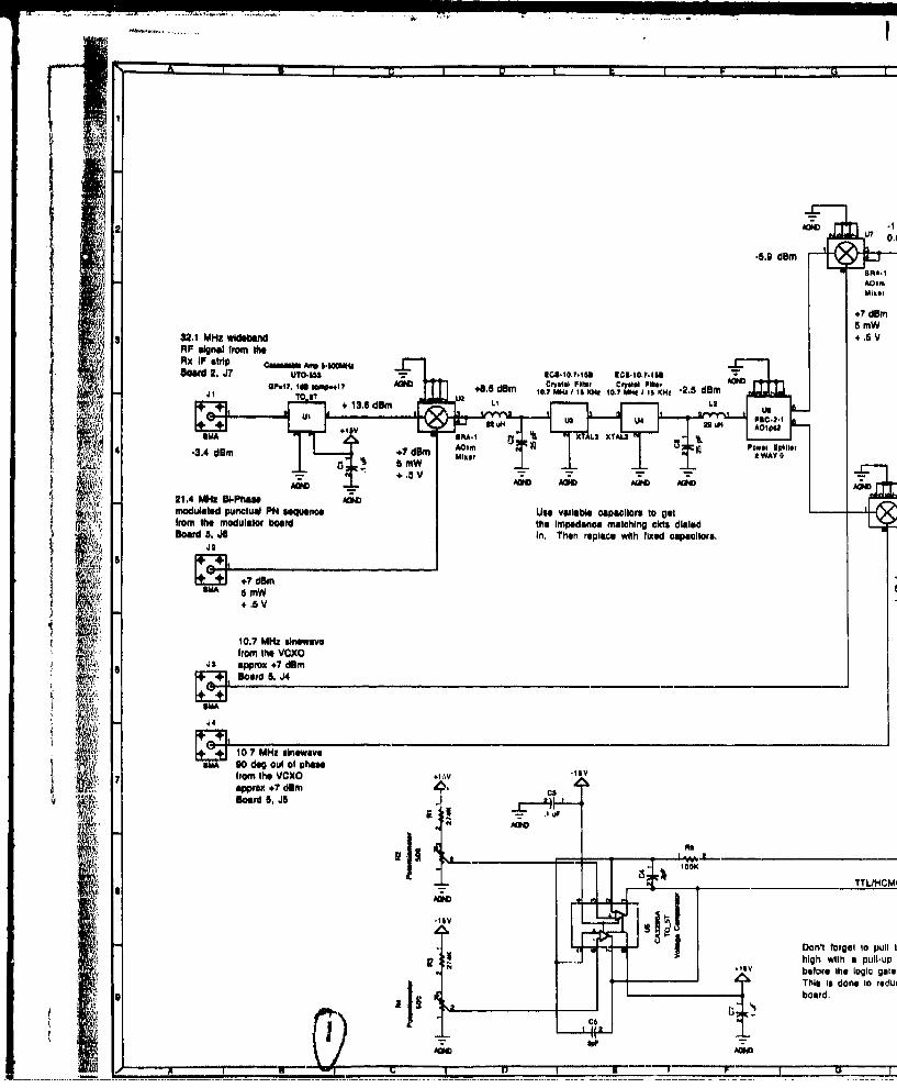
-5.0 d~m * R-
Mixer
+7 drim5 mw
332.1 MHz wideband + .6 VFIX IF strip Caed AW -6MBoard 2, J7 UTO.533 -isi.-s
TO.I +i 13. dAY L1L2
01.4 Um U4 Phase2a1
ard a, AO Pone ThOrelcebthiteeapctos
aMA"
iV21.7 MHz sinewavo AD
*from the Vouao oarXhOmeanemthn ctsdae
Board S. A nJhnrplc4ihfxe aaios
aMA 6m
from ith VCXO FIVis approx +7 dim
Board 6. A5AG
'I"
j.n forge IopisWAig wi0 ao put o phas
bfrom the Vogc at
BoardoardA
AqMG
_ _ _ __ _ _ _ _ _ _ F__ll

+11 B
(CA CIAV
*2
Mee
e Inc thKnert n
data wilt goot nthslieADMedac iolng forbm I FI
c-rrie synchoN Ctio
* TTLMCMO oometi loser deacno Iitnalato, dapettion d andcomarao
Aon Ctrge to purcul the clmdutputeS Ko ti bad
Milo `0V bTfor teepin the~ gateo copnet thn this bobdoard.
AGM Ce -= -- L) t:- .1 upo
A u p A U M 1 - 1 r1 n

cis
C13
1.6 rp Fl144 14A-2644
ilK 2
C14 ACie J
Inert ar, integrator, sample & hold, and comparator.1 uPcircull to demodulate the *PSK on this board.
4 T Thue keeping the analog oomponents on this board.
-7 dbm0.1 V3
ICI
U14 .
cis AD633 -1sv
haguCi 4uIIuUII Aub - UI IO up
A0WM AMC
cis Cal
Aropilitlation before the loop tillerusing a non-Inverting op-amp.
IRI
Coherent BDPSK signal, 7Onoe the Integrate anddump ckit Is inserted, tindata will go out on thiseline.
AG;W AQWFeeodback voltage for
________________________________carrier synohionlzation .russe

I N I I __ I H
Snwsw~ O"Alt, AG
.16V Alli O&V 00.611YSIO o IW1 W
a of
VOXO cordlm voltage. le.*.ack Imm ft0 Costae LootI AA
.I V
77
MWIN+1.9 dam AIo
943,6 dam WlUI 7 4 dm VISI
V.Ads) AM A4 W!PA -a po i
V 4- - -
WAIN4
1071 MHz fixed simowtaw
IA 4.3.6 damAl
Poll II
Alk 'I INow Oplo. I VIbyItA
(IA
Tootl Pboll before b~4m A;lOofl.B
widimortsI Lead wIh 6 SONN11
Is 1*- 14,66" No
ALM4 Mit) aOH
_i (9 _ __
III,to~

To ine Cc
Gan1610?7 MHz .mav ci Ithe D4-t Fu 90 d" out of ph*" Bo a rd 4.,
AOS ofrom tr7 VOX
1 ), NiS esrewve UAsl0 10.4 4m ~r.. D
11 0 dl NA-61. lfeidi 0
orAtlrpHM 1-1 Board ka" To ft~ C4
IF-fl 2S f2.3 *3s To the 0
III 495 oard 4
*17 tI Ulf 4 fibre '- dbM HA S60d
Aid 21 4 MHz bi-phmes rmodulaled
Amd)APM10 wih* pntalP ecuio
ci rppro +71 00m
IoF
.55 '1Y J
4.7.5d~m lo A AM, U1621.4V MHX bi-phiso modulatedP&-61 4 bmwihr a +112To PN "quliAoW?~~Apo
.7S 47Dm N-6
.I',
Early PNAQPr 0.* Ia4 to tS Tr
77. Board 3.
.1 m jr . 4 dbm *7 drr 2t 4 MHz bIIrlales fiod lte.IdAo-f lot with a I1/2Td PN soiquesco
I I AT
ootA
M
11, a -121 4 MHz bi-phita. modulated Do.rdMINDwith an raclotrle of So. punctualum .rc
ATA .~mw Atbmr A, A
r~rrtoe Frod
1 10I
Gain Omi 6 TS.Cit
Tht Frot.
apqtroo .7 dism
rsd AU t0 13011 1P
LOrN. -I~ii Orm till NIl drnw" IDef edosI,~JU d0m 11o ra
*060 ~ u H18 le0~ Ii~ Wtrd. r
114A I i00. 4tA.0
INt V-al

m____ -1.,
10 7 111Is ebieeV.
1WA
To tie Coebe LOWP
10.7 M H z inA~ 0 Vi. D - noduld b lar
itsW, the VCXC jIWO) Ij~pt~l 7 dSn !!I
.7 lob ii the DemnodulatorP~~w Board 4,.J
0. To ft ile euodsaibor
Inn
-1 dnV4 MHz bi*pheee moduletd
-CIII Ill ft~ teI 0pun Opctual .1*ltuico W
ot ppro +7nen 4pinoe4
un I,.1
2, I MHkfwee Jlqipto .GM
AIM
Aim. to thle ITral @Miiet~iOle Bor 3.iA
-7~~T dthe Pelt aAnqt PNsedlon
K1vApo deg od a ie."m
Iin
~-Z. reOO

a a
I -- A
-4,- A -
1.

LAA
a ON
AIr
L~--ý ca
CA -. __________________

-- Lc_ _--_ __ _ AGO9-
,noAt
ff99 99,
La M
3e 9m
UL cc ff -A9P.I.
&DAD 1AUM 1.a
a" ilk

0_.so U, 6 m
U ~Jl:•ra
V,0 SCIO
0 40 CED
a, at 30I
U9 J1&"
Figure D-14 Layout diagram for Board 2 the Rx IFAmplification, AGC, and Detection circuits.
OTI

0 0 0 0
a aoU
On a
a I 0 a
0 •
0 60
0
Laa
Figure D-15 Component side of Board 2.
1 84
a 0
' I LD

C) -) - 2 *2
0
i001
fit
p..~
1~ 0
or
Figure D-16 Sold.r side of Board 2.
85

KIIWT~13
00•. .0o
9 0 9
Figure D-17 Layout diagram for Board 3 the PN Sequenceand Tracking circuits.
86

0
67~~ 00• "b@ 0, 0 "' oooo ,.
S•.• 0 a 0 9 0 0 0.
6 6o o6:,,t 9•a
0 0 U . '"0
0 0 "' l10] €
aan 0 0 0
0I
0 • 0 0 0 "- 1 00 -
•0 , 0 .
o 0" 0
00000
00(
13 13____ ' ,
g e on B.'
0 "-0 -
0 to
0000
Figure D-18 Component side of Board 3.
87

F --- ý.:008a
0.. 0, 0o( a 00
7 []0 0 [
0 i
00, 0
0
0 a0 0
?*. • .'... '.... 0 .6
0'--0 a 0°0 a,. 1
a 0 [] • 0
0xa 0 0 •
[0 a1 a] 0
S•0 0
Figure D-19 Solder side of Board 3.
88

R8
J0 1 us0 IS C2 C SUr- 7.0- 11 u13 cC 4.) •.. R4 R31
06 s
0I /30~ CIS @ IlU 021 ' 2 jC, U
CIS0 C2 ig
ci Rt R1I fJC 23A U2 L4 OR
R14
J5
AFigure D-20 Layout diagram for Board 4 the Carrier
Tracking Loop and Demodulator circuits.
-' 89

V 4
t.1 0)
a 0~
0- ft MC
I l k .- . - . .*0 u~0* 0
L!g .
=70 ~ tIso
=07
L !.-Y
16N
Figure D.21 Layout diagram for Board 5 the Modulationand Amplification circuits,
90

0
000000o 0000000@0000
000 00 0 000000000004000 .0,0aU 0 0 0 00a 0 0-00 a7 0 0 0
P 0 00 a 3
0 0.
0 00
no a:00 @0.1 0 0 0a 0' -
0 0 003 0
a@0 a0 a
3@ 0
13 0."000 00
0 U0 00 3l0 0000 -a
*' a 00'0 @0 a 90
"o 0 7
03 0 @0 0 00)
.0 00 00 '0,
00 0017. 0 0U
0 0a a 0 01
0 00 0
0 0 a
0
00
0- ag0
Figure D-22 Component side of Board 5.

O pq 3-O 0-- 0- 0
0.'
00
U0 0
l -0 0 0
00
0-" -0---0
00
I I 0331_ _ _ _ _ _ _ _ _ _ _ _ _ _ _ _ _0 0,
0 a_ ''
0 0
0 0
Figure D-23 Solder side of Board 5.
92

LIST OF REFERENCES
[1] Couch, L., Digital and Analog Communication Systems, Macmillian PublishingCompany, New York, NY, 1990.
[2] Williams, F., and Sloane, N., "Pseudo-Random Sequence and Arrays," Proceedingsof the IEEE, vol. 64, No. 12, 19 76 , pp. 1715-1729.
[3] Proakis, J., Digital Communications, McGraw-Hill Book Co., New York, NY, 2nded., 1989.
[4] Welti, A., "Doppler Arceleration Influence on Code Tracking in Direct SequenceSpread Spectrum Systems," IEEE GLOBECOM, vol. 3, 1989, pp. 1624-1628.
[5] Simon, M., Omura, J., Scholtz, R., and Levitte, B., Spread SpectrumCommunications, vol. III, Computer Science Press, Rockville, MD, 1985.
[6] Avantek, Modular and Oscillator Components, Avantek Inc., Milpitas, CA, 2nded., 1990.
[7] Holmes, J., Coherent Spread Spectrum Systems, John Wiley and Sons, New York,NY, 1982.
[8] MiniCircuits, RF/IF Designer's Handbook, Scientific Components, Brooklyn, NY,1992.
[9] Polydoros, A. and Weber, C., "A Unified Approach to Serial Search Spread-Spectrum Code Acquisition-Part I: General Theory," IEEE Transactions onCommunications, vol. COM-32. No. 5, 1984, pp. 542-549.
[10] Polydoros, A. and Weber, C., "A Unified Approach to Serial Search Spread-Spectrum Code Acquisition-Part II: A Matched-Filter Receiver," IEEETransactions on Communications, vol. COM-32, No. 5, 1984, pp. 550-560.
[11] Dixon, R., Spread Spectrum Systems, John Wiley and Sons, New York, NY, 2nded., 1984.
[121 Tietze, U., and Schenk, C., Electronic Circuits Design and Applications,Heidelberg, Springer-Verlag Berlin, 1991.
[131 Analog Devices, Special Linear Reference Manual, Analog Devices Inc.,Norwood, MA, 1992.
93

INITIAL DISTRIBUTION LIST
Defense Technical Information Center 2Cameron StationAlexandria, Virginia 22304-6145
2. Library, Code 52 2Naval Postgraduate SchoolMonterey, California 93943-5101
3. Chairman, Code ECDepartment of Electrical and Computer EngineeringNaval Postgraduate SchoolMonterey, California 93943-5121
4. Prof. T. Ha, Code EC/HaDepartment of Electrical and Computer EngineeringNaval Postgraduate SchoolMonterey, California 93943-5121
5. Prof. R. Panholzer, Code SP 2Department of Electrical and Computer EngineeringNaval Postgraduate SchoolMonterey, California 93943-5194
6. LT Arnold 0. Brown III200 S. Fairfax St.Dumfries, Virginia 22026
L9