near east university faculty of engineeringdocs.neu.edu.tr/library/4854587856.pdf · ·...
TRANSCRIPT

Faculty of Engineering
NEAR EAST UNIVERSITY
Department of Electrical and Electronic Engineering
LIGHT ACTIVATED ALARM CIRCUIT
Graduation Project EE - 400
Student: Fatma ikbal TEMiZ (20032648)
Supervisor: Asst. Professor Dr. .. .. Ozqur C. Ozerdem
Nicosia - 2007

• / , .;;;r ( ·~ /~/,~\ v'
';.:~ ~.M \ ·~
~ \¥ "11 ~ /{)/:
' ,,,;-·,'/ ~~ ·' 8 ~ t~~(::_.;:~,t
Ozerdem to be'Toy''"_:::>'
ACKNOWLEDGEMENTS
First I want to thank to Asst. Prof. Dr. Ozgur C.
advisor. Under his guidance, I successfully overcome many difficulties and
learn a lot about designing and building circuits, and I also learn different kind
of circuit elements. In each discussion, he always answer my questions
patiently, and I felt my quick progress from his advices. He always helps me in
my study and my life. I asked him many questions about electricity and
electronics, and about work life, and he always answered my questions.
I also thank to Mr. Kamil Dimililer for his advices. And my special
thanks to my friends Davut Isiker and Fatih Giinde. With their endless help, I
could see and overcome my some mistakes in designing and constucting my
circuit. Thanks to Faculty of Engineering for having good electronics labotory.
Finally, I want to thank to my family, especially my parents. Without
their endless support and love for me, I would never achieve my current
position. I wish my mother and my father lives happily with me during my life
time always.

•
ABSTRACT
The purpose of any alarm system is to either protect life or property or
to detect an intrusion. Many buildings and complexes being constructed today
are equipped with some type of intrusion detection and fire alarm systems.
Also in the homes, some alarm systems are used, for example burglar alams,
light alarms etc. Numerous detection and fire alarm systems are in existence
today. An alarm gives an audible or visual warning of a problem or condition.
These noisy reminders tell us when the things in our lives are not right. That is
why we need information before choosing an alarm. Using this information we
can make decisions about the alarm needed. This project presents the design, construction and testing of a light-
activated alarm. The principle of operation of this light-activated alarm is
simple. When the intensity of light exceeds certain intensity, that is, when a
light beam is shone into the sensor, the alarm is triggered and buzzer alarm
begins to operate and sounds an alarm. Alarm sounds and the LED flashes.
These actions thus alert the owner of the residence and/or security personnel of
the presence of an intruder. In all light-operated alarms, LDR is used as a light sensing element.
The LDR is light-dependent resistor, and this light dependent resistor is a
cadmium-sulphide photocell, and acts as a high resistance under dark
conditions and as a low resistance when brightly illuminated.
In each circuit, l.d.r. is mounted in a normally dark area and the designs
are such that the alarm sounds when a light shone into the protected area. The
ldr and a potentiometer (variable resistor) form a potential divider that supplies
the darligton pair. Under dark conditions the 1.d.r. presents a high resistance, so
zero drive applied to darlington pair transistors. When l.d.r. is illuminated, its
resistance falls to a low value, and darlington pair is then applied to buzzer and
activates the alarm. When the LDR resistance falls to less than 200kQ in this
circuit, alarm is activated.
11
- -- ------- ' I'
TABLE OF CONTENTS
ACKNOWLEDGEMENTS
ABSTRACT 11
CONTENTS 111
INTRODUCTION VI
1. USING BREADBOARDS 1
1.1. Overview 1
1.2. How it works 1
1.3. Naming history 3
1.4. Using the breadboard 4
1.5. Wiring techniques 5
2. BATTERY 7
2.1. Overview 7
2.2. Classification of batteries 9
2.3. How Batteries work 9
2.4. Battery Capacity and Discharging 10
2.5. Battey life 11
2.6. Conversion to energy 12
2.7. Battery Lifetime 12
2.8. Battery Explosion 13
2.9. Rechargeable and disposable batteries 13
2.10 Disposable ( non-rechagreable) batteries 14
2.11 Rechargeable batteries 15
3. RESISTORS 17
3 .1. Overview 17
3 .2. Variable resistor 18
3.1.1 Potentiometer 20
3.1.2 Rheostat 23
3 .1.3 Theory of operation of potentiometer 23
3 .1.4 Applications of potentiometer 24
111

•
4. DIODES 26
4.1. Overview 26
4.2. Semiconductor diode 27
4.3. Types of Semiconductor Diodes 29
4.4. Applications of diodes 29
5. LEDS 30
5.1. Overview 30
5.2. Physical function of led 31
5 .3. What is Inside an LED? 32
5.4. What Causes LED to Emit Light and What Determines
the Color of the Light 33
5.5. How Much Energy Does an LED Emit? 33
5.6. LED applications 34
5.7. Illumination Applications of LED 35
6. TRANSISTORS 37
6.1. Overview 37
6.2. Importance 43
6.3. Types of transistors 43
6.4. Semiconductor materials 46
6.5. Packaging 47
6.6. Usage of Transistors 48
6.7. Transistor codes 53
6.8. Choosing a Transistor 54
7. DARLINGTON PAIR OF TRANSISTORS 55
7.1 Overview 55
8. TheLDR
8.1. Overview 54
8.2. Applications of LDR
58
59
IV

•
8.1.1 LIGHT SENSORS
8.1.2 PHOTORESISTORS
59
63
9.1 Overview
65
65
9. BUZZERS
10. Testing of the electronic devices with a DMM
10.1 Testing Battery
10.2 Transistor testing methodology
10.3 Testing Darlington Transistors
10.4 Testing LEDS
10.5 LDR Testing
68
68
68
71
71
72
11.1 Results of testing the circuit elements
74
77
11. CIRCUIT DIAGRAM AND RESULTS
CONCLUSION
REFERENCES
79
80
APPENDICES 82
V
---- - - - _- - - - ~ - - -~ -- I
INTRODUCTION
The desing of an electronic circuit requires a priori information about
the operation and connection procedures of electronic circuit elements. Using
the breadboard, connection procedures of the breadboard and the elements, and
why they are used in that circuit must be known before building a circuit.
When these informations are not known completely, several mistakes might be
done, elements may be bum and the circuit built may not operate.
An alarm circuit or an alarm system is one of the most important aspect
of the security system. Alarms as the name implies are used to alert in the event
of any situation that is a threat. The ability to sense the things and give an
alarm sound for that which the alarm is sensitive, provide security in our homes
or any building.
The purpose of any alarm system is to either protect life or property or
to detect an intrusion. Many buildings and complexes being constructed today
are equipped with some type of intrusion detection and alarm systems. Also in
the homes, some alarm systems are used, for example burglar alams, fire
alarms, light alarms etc. Numerous detection and fire alarm systems are in
existence today.
This project is aimed to provide an light-activated alarm using in the
homes and buildings which has to be in normally dark conditions. When a light
is entering to that place, the alarm will give a sound. The construction is based
on the sensitivity of the alarm.
The project consists of eleven chapters and conclusion. First 10
chapters introduces the circuit elements used in the light-activated alarm
circuit, and gives information and test conditions about circuit components.
Last chapter, the circuit diagram and test results were introduced.
VI

CHAPTER 1. USING BREADBOARDS
1.1 Overview Breadboard is a thin plastic board full of holes used to hold electronic
components (transistors, chips, etc.) that are wired together. It is used to develop
electronic prototypes or one-of-a-kind systems circuit. A breadboard is a reusable solderless device used to build a (generally
temporary) prototype of an electronic circuit and for experimenting with circuit designs.
A typical breadboard will have strips of interconnected electrical terminals, known as
bus strips, down one or both sides either as part of the main unit or as separate blocks
clipped on to carry the power rails. A modem solderless breadboard consists of a perforated block of plastic with
numerous tin plated phosphor bronze spring clips under the perforations.
Interconnecting wires and the leads of discrete components (such as capacitors,
resistors, inductors, etc.) can be inserted into the remaining free holes to complete the
circuit topology. In this manner, a variety of electronic systems may be prototyped,
from small circuits to complete central processing units (CPUs). However, due to large
stray capacitance (from 2-25pF per contact point), solderless breadboards are limited to
operating at relatively low frequencies, usually less than 10 MHz, depending on the
nature of the circuit.
1.2 How it Works The heart of the solder-less breadboard is a small metal clip. The clip is made of
nickel silver material which is reasonably conductive, reasonably springy, and
reasonably corrosion resistant. Because each of the pairs of fingers is independent we
can insert the end of a wire between any pair without reducing the tension in any of the
other fingers. Hence each pair can hold a wire with maximum tension.
To make a breadboard, an array of these clips is embedded in a plastic block
which holds them in place and insulates them from each other, like this:
1

•
Figure 1.1 a breadboard array
Depending on the size and arrangement of the clips, we get either a socket strip
or a bus strip. The socket strip is used for connecting components together. It has two
rows of short (5 contact) clips arranged one above another, like this:
!!!!!~!!!!!~!!!!!!!!!!!!!~!!!!!!!!!~!!!!!!!!!~!!!!!!!!!~!!~!!!!!
iiiiiiiiiiiiiiiiiiiiiiiiiiiiiiiiiiiiiiiiiiiiiiiiiiiiiiiiiiiiiiii Figure 1.2 breadboard socket strip connections
The bus strip is used to distribute power and ground voltages through the circuit.
It has four long clips arranged lengthwise, like this:
Figure 1.3 breadboard bus strip connections
Note that in their infinite wisdom, the manufacturer elected not to join the
adjacent contact strips into a single full-length contact strip. If this is what you want,
you will have to bridge the central gap yourself.
When we combine two socket strips, three bus strips, and three binding posts on
a plastic base, we get the breadboard. The breadboard offers an easy way to build
electrical circuits without soldering. The 2 "x3" breadboard contains an array of holes
where wires and components are to be inserted. The holes in the center portion of the
breadboard are identifiable by row (vertical in the photos) and column (horizontal).
2
~ --------
•
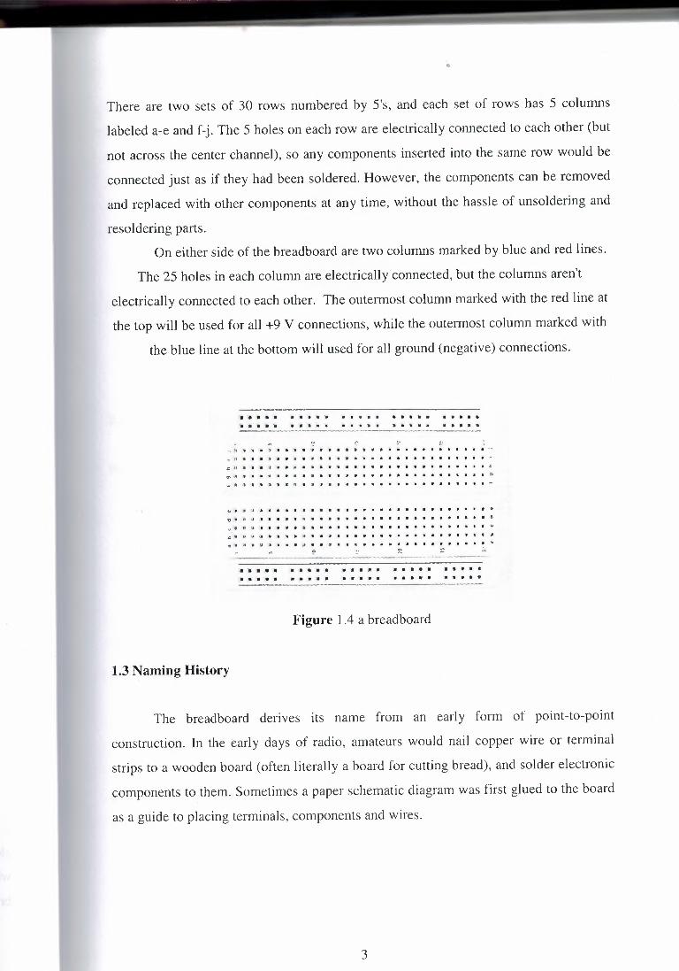
There are two sets of 30 rows numbered by S's, and each set of rows has 5 columns
labeled a-e and f-j. The 5 holes on each row are electrically connected to each other (but
not across the center channel), so any components inserted into the same row would be
connected just as if they had been soldered. However, the components can be removed
and replaced with other components at any time, without the hassle of unsoldering and
resoldering parts.
On either side of the breadboard are two columns marked by blue and red lines.
The 25 holes in each column are electrically connected, but the columns aren't
electrically connected to each other. The outermost column marked with the red line at
the top will be used for all +9 V connections, while the outermost column marked with
the blue line at the bottom will used for all ground (negative) connections.
• ~ • • • • • • ~ • • • • • ~ • • • Ii • • ~ • • •
~ ~ • ~ • ~ • ~ ~ • • ~ ~ • ~ • j ~ • • ~ ~ • • •
0 ,r, c;. •• ~ - ~ "" -'11 1' 'I a <I ca• :'I• 0'1 '.• '• •. • "M • • • •••••••It•,.-~ - ~ 11 C'I ,. ll "'I' ,. ::J • I S I 1i • • :II • • • • -• • • .• Ii • • 'f • •
:::1'1ci'••i1:.:sli•••'.•'II:•••••········ .,,c Ql'ii'l'.Jl'.99-ll.~ .• -~················· 11Cll -ll-'.tlll'tl~lill················· ._ ••..
(Ii,,. u .;1 11 .i--. 11,,. • '• • • • • • • • • • • • • • • •, • ~
<of• 11 lt .) jl • '9 • i- .•• • .• • _. • • I • • • • • • • • I • 11 f; I C
1,.,.\• It II ;1 I 'jf 'II .• (I 11 I • I I a I I • a • ·a I • • a I 'I I t I' V
~\ii II u U1 I .I • ll It Ii 'ti • • :ti • • • • • 1 • .• • • • 1 1 Ii a: I' II
<?l'I ~ ·it ·i, l ~.JI. it:•, ••• ,, •••• ii •••••••••• ,, ~ ~ ~ . . ~ ~ . . . ~ ~ . . . ~ . . ~ . . . , . . . . . • ~ • ~ ~ ~ ~ • ~ • ~ ~ ~ • • • • • • • j • • • •
Figure 1 .4 a breadboard
1.3 Naming History
The breadboard derives its name from an early form of point-to-point
construction. In the early days of radio, amateurs would nail copper wire or terminal
strips to a wooden board (often literally a board for cutting bread), and solder electronic
components to them. Sometimes a paper schematic diagram was first glued to the board
as a guide to placing terminals, components and wires.
3

Figure 1.4 A breadboard with a completed circuit
1.4 Using the Breadboard The bread board has many strips of metal (copper usually) which run underneath
the board. The metal strips are laid out as shown below.
Figure 1.6 connections
These strips connect the holes on the top of the board. This makes it easy to
connect components together to build circuits. To use the bread board, the legs of
components are placed in the holes (the sockets). The holes are made so that they will
hold the component in place. Each hole is connected to one of the metal strips running
underneath the board.
Each wire forms a node. A node is a point in a circuit where two components are
connected. Connections between different components are formed by putting their legs
4

in a common node. On the bread board, a node is the row of holes that are connected by
the strip of metal underneath.
The long top and bottom row of holes are usually used for power supply
connections. The rest of the circuit is built by placing components and connecting them
together with jumper wires. Then when a path is formed by wires and components from
the positive supply node to the negative supply node, we can tum on the power and
current flows through the path and the circuit comes alive.
For chips with many legs (ICs), place them in the middle of the board so that
half of the legs are on one side of the middle line and half are on the other side.
1.4 Wiring Techniques The basic idea of wiring on a solder-less breadboard is simple: just stick the ends
of the component leads or wires into the holes. But like any seemingly simple process,
there are a few subtleties that can make the difference between success and failure.First
a note of caution, the material that the clips inside the breadboard are made of is a
compromise between good conductivity, corrosion resistance, and springiness.The
elastic limit is considerably less than of a good steel spring and if spread too far, can be
permanently distorted. To avoid deforming the connector clips, never insert more than
one wire in a hole.With the health of our breadboard assured, there are a few more
things we can do to make sure that our connections are good ones.
Strip about 5 mm of insulation from each end of a piece of wire. Less than that
raises the risk that insulation will be forced between the fingers of the clip. More leaves
bare wire exposed that can short to adjacent components. One exception: strip about 15
mm from the end of a wire that will be clamped in the binding posts.
When inserting a small wire or component, use your needle nosed pliers rather than
your fingers to hold it. If the end of a wire becomes kinked, cut it off or use your pliers
to straighten- it.
The solderless breadboard is a tool for rapid circuit development and assembly,
in which design changes can easily be made. The breadboard is typical of most versions
and skill in using it is essential for the practicing engineer.
The holes in the board reside over conducting metal spring clips into which
component leads can be inserted. The conducting spring clips run lengthwise in the thin
fields and vertically, in groups of five, in the fat fields.
5
•
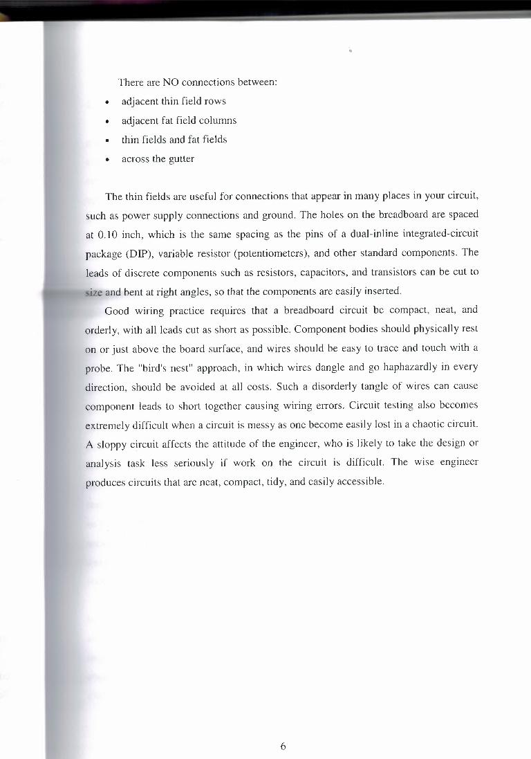
There are NO connections between:
• adjacent thin field rows
• adjacent fat field columns
• thin fields and fat fields
• across the gutter
The thin fields are useful for connections that appear in many places in your circuit,
such as power supply connections and ground. The holes on the breadboard are spaced
at 0.10 inch, which is the same spacing as the pins of a dual-inline integrated-circuit
package (DIP), variable resistor (potentiometers), and other standard components. The
leads of discrete components such as resistors, capacitors, and transistors can be cut to
size and bent at right angles, so that the components are easily inserted.
Good wiring practice requires that a breadboard circuit be compact, neat, and
orderly, with all leads cut as short as possible. Component bodies should physically rest
on or just above the board surface, and wires should be easy to trace and touch with a
probe. The "bird's nest" approach, in which wires dangle and go haphazardly in every
direction, should be avoided at all costs. Such a disorderly tangle of wires can cause
component leads to short together causing wiring errors. Circuit testing also becomes
extremely difficult when a circuit is messy as one become easily Jost in a chaotic circuit.
A sloppy circuit affects the attitude of the engineer, who is likely to take the design or
analysis task less seriously if work on the circuit is difficult. The wise engineer
produces circuits that are neat, compact, tidy, and easily accessible.
6

CHAPTER 2. BATTERY
2.1 Overview An electrical device that converts chemical energy into electrical energy,
consisting of a group of electric cells that are connected to act as a source of direct
current. The term is also now commonly used for a single cell, such as the alkaline dry
cell used in flashlights and portable tape players, but strictly speaking batteries are made
up of connected cells encased in a container and fitted with terminals to provide a
source of direct electric current at a given voltage. A cell consists of two dissimilar
substances, a positive electrode and a negative electrode, that conduct electricity, and a
third substance, an electrolyte, that acts chemically on the electrodes. The two
electrodes are connected by an external circuit (e.g., a piece of copper wire); the
electrolyte functions as an ionic conductor for the transfer of the electrons between the
electrodes. The voltage, or electromotive force, depends on the chemical properties of
the substances used, but is not affected by the size of the electrodes or the amount of
electrolyte.
Batteries are classed as either dry cell or wet cell. In a dry cell the electrolyte is
absorbed in a porous medium, or is otherwise restrained from flowing. In a wet cell the
electrolyte is in liquid form and free to flow and move. Batteries also can be generally
divided into two main types : rechargeable and nonrechargeable, or disposable.
Disposable batteries, also called primary cells, can be used until the chemical changes
that induce the electrical current supply are complete, at which point the battery is
discarded. Disposible batteries are most commonly used in smaller, portable devices
that are only used intermittently or at a large distance from an alternative power source
or have a low current drain. Rechargeable batteries, also called secondary cells, can be
reused after being drained. This is done by applying an external electrical current, which
causes the chemical changes that occur in use to be reversed. The external devices that
supply the appropriate current are called chargers or rechargers.
A battery called the storage battery is generally of the wet-cell type; i.e., it uses a
liquid electrolyte and can be recharged many times. The storage battery consists of
several cells connected in series. Each cell contains a number of alternately positive and
negative plates separated by the liquid electrolyte. The positive plates of the cell are
connected to form the positive electrode; similarly, the negative plates form the negative
electrode. In the process of charging, the cell is made to operate in reverse of its
7
--=- ~-.-=----·---~
discharging operation; i.e., current is forced through the cell in the opposite direction,
causing the reverse of the chemical reaction that ordinarily takes place during discharge,
so that electrical energy is converted into stored chemical energy. The storage battery's
greatest use has been in the automobile where it was used to start the internal
combustion engine. Improvements in battery technology have resulted in vehicles in
which the battery system supplies power to electric drive motors instead.
Batteries are made of a wide variety of electrodes and electrolytes to serve a
wide variety of uses. Batteries consisting of carbon-zinc dry cells connected in various
ways (as well as batteries consisting of other types of dry cells) are used to power such
devices as flashlights, lanterns, and pocket-sized radios and CD players. Alkaline dry
cells are an efficient battery type that is both economical and reliable. In alkaline
batteries, the hydrous alkaline solution is used as an electrolyte; the dry cell lasts much
longer as the zinc anode corrodes less rapidly under basic conditions than under acidic
conditions. A more expensive type of lead-acid battery called a gel battery (or gel cell)
contains a semisolid electrolyte to prevent spillage. More portable rechargeable batteries
include several dry-cell types, which are sealed units and are therefore useful in
appliances like mobile phones and laptops. Cells of this type (in order of increasing
power density and cost) include nickel-cadmium (nicad or NiCd), nickel metal hydride
(NiMH), and lithium-ion (Li-Ion) cells.
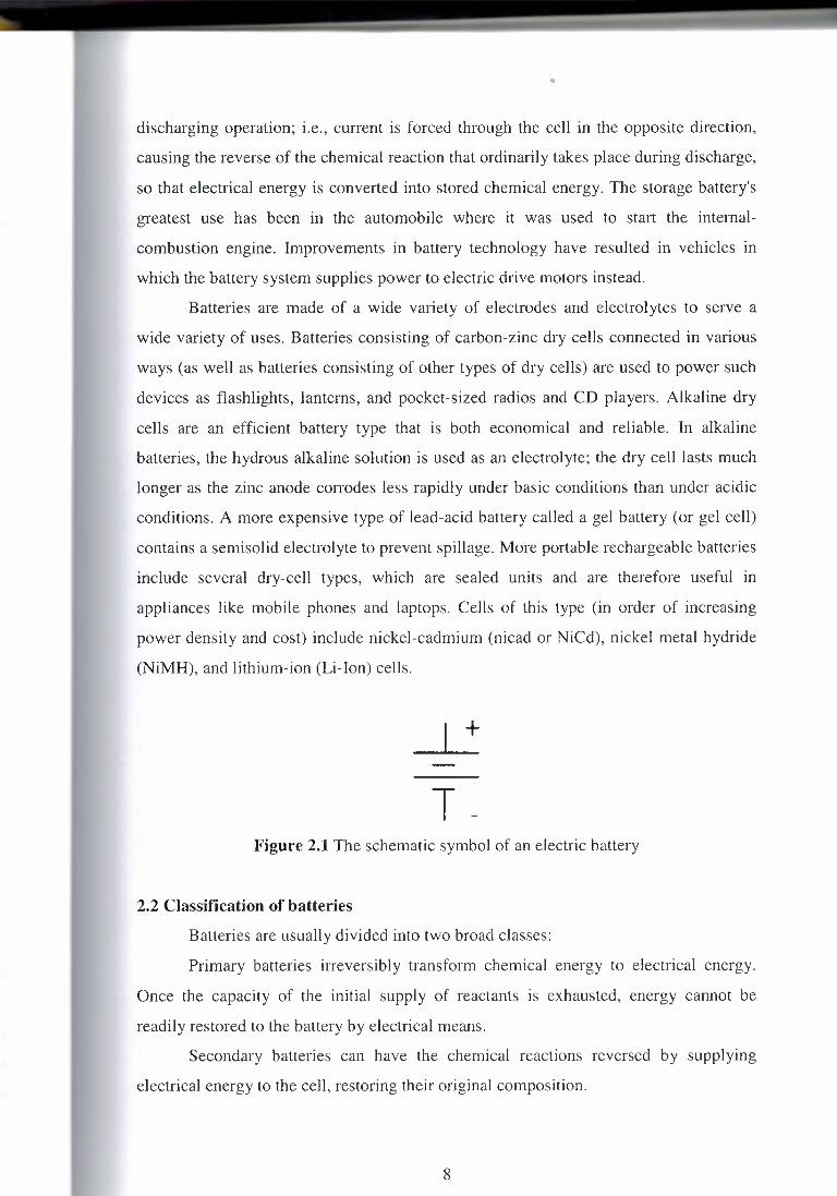
+
Figure 2.1 The schematic symbol of an electric battery
2.2 Classification of batteries
Batteries are usually divided into two broad classes:
Primary batteries irreversibly transform chemical energy to electrical energy.
Once the capacity of the initial supply of reactants is exhausted, energy cannot be
readily restored to the battery by electrical means.
Secondary batteries can have the chemical reactions reversed by supplying
electrical energy to the cell, restoring their original composition.
8
··--·------
2.3 How batteries work
Battery consists of one or more voltaic cells, each of which is composed of two
half cells connected in series by the conductive electrolyte. Each cell has a positive
terminal, and a negative terminal. These do not touch each other but are immersed in a
solid or liquid electrolyte.
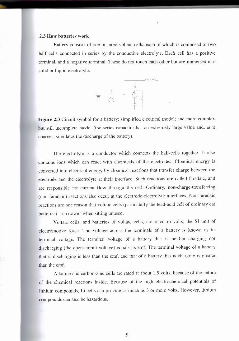
Figure 2.3 Circuit symbol for a battery; simplified electrical model; and more complex
but still incomplete model (the series capacitor has an extremely large value and, as it
charges, simulates the discharge of the battery).
The electrolyte is a conductor which connects the half-cells together. It also
contains ions which can react with chemicals of the electrodes. Chemical energy is
converted into electrical energy by chemical reactions that transfer charge between the
electrode and the electrolyte at their interface. Such reactions are called faradaic, and
are responsible for current flow through the cell. Ordinary, non-charge-transferring
(non-faradaic) reactions also occur at the electrode-electrolyte interfaces. Non-faradaic
reactions are one reason that voltaic cells (particularly the lead-acid cell of ordinary car
batteries) "run down" when sitting unused.
Voltaic cells, and batteries of voltaic cells, are rated in volts, the SI unit of
electromotive force. The voltage across the terminals of a battery is known as its
terminal voltage. The terminal voltage of a battery that is neither charging nor
discharging (the open-circuit voltage) equals its emf. The terminal voltage of a battery
that is discharging is less than the emf, and that of a battery that is charging is greater
than the emf.
Alkaline and carbon-zinc cells are rated at about 1.5 volts, because of the nature
of the chemical reactions inside. Because of the high electrochemical potentials of
lithium compounds, Li cells can provide as much as 3 or more volts. However, lithium
compounds can also be hazardous.
9

• - - I
•
The simplest characterization of a battery would give its emf (voltage), its
internal resistance, and its capacity. In principle, the energy stored by a battery equals
the product of its emf and its capacity.
2.4 Battery capacity and discharging Since the voltage of a battery is relatively constant, the capacity of a battery to
store energy is often expressed in terms of the total amount of charge able to pass
through the device. This is expressed in ampere hours, where one A·h equals 3600
coulombs. If a battery can pump charges for one hour at a rate of one coulomb/sec or
one ampere (1 A), it has a capacity of 1 A·h. If it can provide 1 A for 100 hours, its
capacity is 100 Ah. The more electrolyte and electrode material in the cell, the greater
the capacity of the cell. Thus a tiny cell has much less capacity than a much larger cell,
even if both rely on the same chemical reactions (e.g. alkaline cells), which produce the
same terminal volta~e.
Because of the chemical reactions within the cells, the capacity of a battery
depends on the discharge conditions such as the magnitude of the current, the duration
of the current, the allowable terminal voltage of the battery, temperature, and other
factors.
Battery manufacturers use a standard method to determine how to rate their
batteries. The battery is discharged at a constant rate of current over a fixed period of
time, such as 10 hours or 20 hours, down to a set terminal voltage per cell. So a
100 ampere-hour battery is rated to provide 5 A for 20 hours at room temperature.
The efficiency of a battery is different at different discharge rates. When
discharging at low rate, the battery's energy is delivered more efficiently than at higher
discharge rates. This is known as Peukert's Law. The relationship between current,
discharge time, and capacity is expressed by Peukert's law.
The available capacity of a battery depends on the rate at which it is discharged.
If a battery is discharged at a relatively high rate, the available capacity will be lower
than expected. Therefore, a battery rated at 100 A·h (360000 coulombs) will deliver 20
A (20 coulombs per second) over a 5 hour period, but if it is instead discharged at 50 A
(50 coulombs per second), it will run out of charge before the theoretically expected 2
hours. For this reason, a battery capacity rating is always related to an expected
discharge time, which is typically 5 or 20 hours.
10
In general, the higher the ampere-hour rating, the longer the battery will last for
a certain device. Installing batteries with different A·h ratings will not affect the
operation of a device rated for a specific voltage.
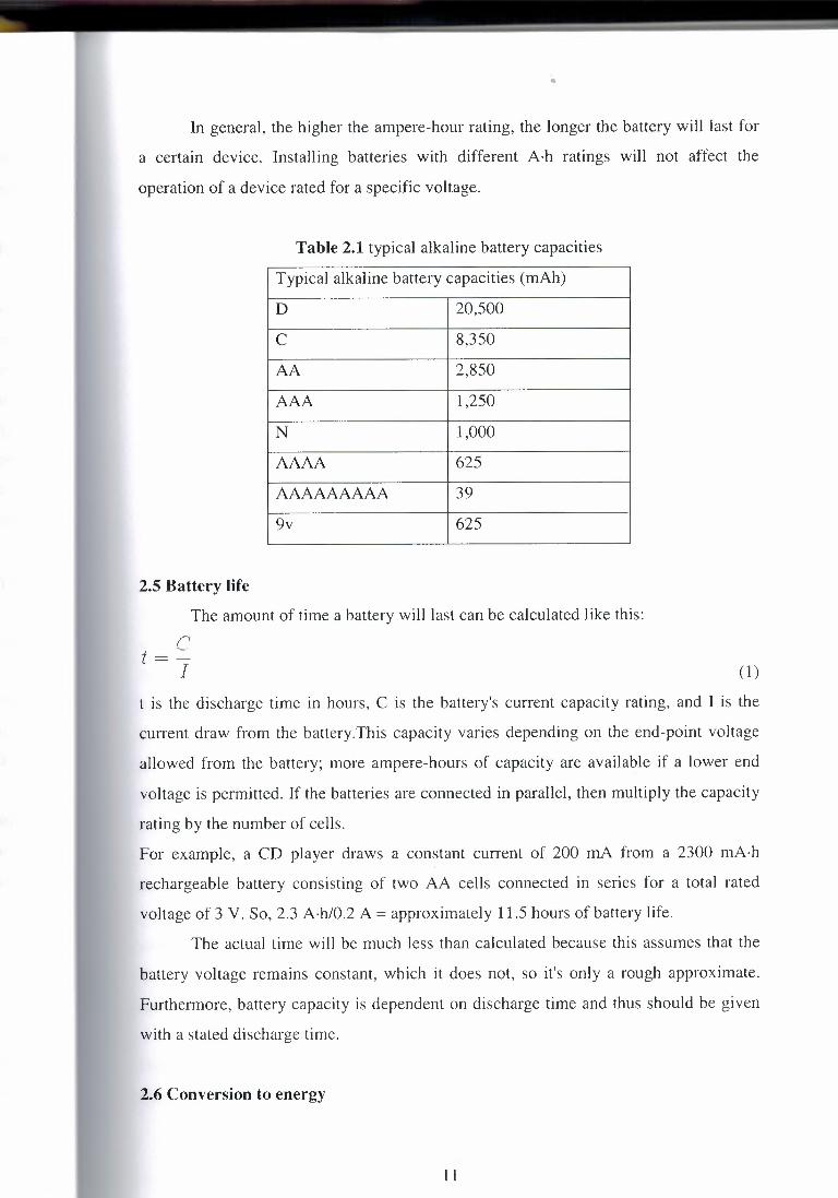
Table 2.1 typical alkaline battery capacities
Typical alkaline battery capacities (mAh)
D 20,500
C 8,350
AA 2,850
AAA 1,250
N 1,000
AAAA 625
AAAAAAAAA 39
9v 625
2.5 Battery life
The amount of time a battery will last can be calculated like this:
(1)
t is the discharge time in hours, C is the battery's current capacity rating, and I is the
current draw from the battery.This capacity varies depending on the end-point voltage
allowed from the battery; more ampere-hours of capacity are available if a lower end
voltage is permitted. If the batteries are connected in parallel, then multiply the capacity
rating by the number of cells.
For example, a CD player draws a constant current of 200 mA from a 2300 mA-h
rechargeable battery consisting of two AA cells connected in series for a total rated
voltage of 3 V. So, 2.3 A-h/0.2 A= approximately 11.5 hours of battery life.
The actual time will be much less than calculated because this assumes that the
battery voltage remains constant, which it does not, so it's only a rough approximate.
Furthermore, battery capacity is dependent on discharge time and thus should be given
with a stated discharge time.
2.6 Conversion to energy
11
The A·h rating of a battery is related to, but not the same as, the amount of
energy it stores when fully charged. If two batteries have the same nominal voltage,
then the one with the higher Ah rating stores more energy. It would also typically take
longer to recharge.
The energy E available from a battery is approximately given by:
E ·~T r- . =Uv v (2)
where, Q is the charge, and V is the nominal voltage.
This yields:
number of joules = number of ampere-hours x number of volts x 3600 seconds per
hour, or number of watt-hours= number of ampere-hours x number of volts.
This is only an approximation though, due to the fact that the voltage during
discharge is not actually constant.
2.7 Battery lifetime
Even if never taken out of the original package, disposable ( or "primary")
batteries can lose two to twenty-five percent of their original charge every year. This
rate depends significantly on temperature, since typically chemical reactions proceed
more rapidly as the temperature is raised. This is known as the "self discharge" rate and
is due to non-current-producing chemical reactions, which occur within the cell even if
no load is applied to it. Batteries should be stored at cool or low temperatures to reduce
the rate of the side reactions. For instance, some people make a practice of storing
unused batteries in their refrigerators to extend battery lifetime, although care should be
taken to ensure the batteries do not freeze. Extremely high or low temperatures will
reduce battery performance.
Rechargeable batteries self-discharge more rapidly than disposable alkaline
batteries; up to three percent a day (depending on temperature). Due to their poor shelf
life, they should not be stored and then relied upon to power flashlights or radios in an
emergency. For this reason, it is a good idea to keep alkaline batteries on hand. Ni-Cd
Batteries are almost always "dead" when purchased, and must be charged before first
use.
Most NiMH and NiCd batteries can be charged several hundred times. Also,
they both can be completely discharged and then recharged without their capacity being
damaged or shortened.
12

·.
Special "reserve" batteries intended for long storage in emergency equipment or
munitions keep the electrolyte of the battery separate from the plates until the battery is
activated, allowing the cells to be filled with the electrolyte. Shelf times for such
batteries can be years or decades. However, their construction is more expensive than
more common forms.
2.8 Battery explosion
A battery explosion is caused by the misuse or malfunction of a battery, such as
attempting to recharge a primary battery, or short circuiting a battery. With car batteries,
explosions are most likely to occur when a short circuit generates very large currents. In
addition, car batteries liberate hydrogen when they are overcharged (because of
electrolysis of the water in the electrolyte). Normally the amount of overcharging is
very small, as is the amount of explosive gas developed, and the gas dissipates quickly.
When a battery is recharged at an excessive rate, an explosive gas mixture of
hydrogen and oxygen may be produced faster than it can escape from within the walls
of the battery, leading to pressure build-up and the possibility of the battery case
bursting. In extreme cases, the battery acid may spray violently from the casing of the
battery and cause injury. Additionally, disposing of a battery in fire may cause an
explosion as steam builds up within the sealed case of the battery.
Overcharging, that is, attempting to charge a battery beyond its electrical
capacity, can also lead to a battery explosion, leakage, or irreversible damage to battery.
It may also cause damage to the charger or device in which the overcharged battery is
later used.
2.9 Rechargeable and disposable batteries
From a user's viewpoint, at least, batteries can be generally divided into two
main types: rechargeable and non-rechargeable (disposable). Each is in wide usage.
Disposable batteries, also called primary cells, are intended to be used once and
discarded. These are most commonly used in portable devices with either low current
drain, only used intermittently, or used well away from an alternative power source.
Primary cells were also commonly used for alarm and communication circuits where
other electric power was only intermittently available. Primary cells cannot be reliably
recharged, since the chemical reactions are not easily reversible. Battery manufacturers
13
•
recommend against attempting to recharge primary cells, although some electronics
enthusiasts claim it is possible to do so using a special type of charger.
By contrast, rechargeable batteries or secondary cells can be re-charged after
they have been drained. This is done by applying externally supplied electrical current,
which reverses the chemical reactions that occur in use. Devices to supply the
appropriate current are called chargers or rechargers.
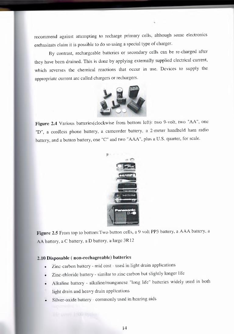
Figure 2.4 Various batteries(clockwise from bottom left): two 9-volt, two "AA", one
"D", a cordless phone battery, a camcorder battery, a 2-meter handheld ham radio
battery, and a button battery, one "C" and two "AAA", plus a U.S. quarter, for scale.
Figure 2.5 From top to bottom:Two button cells, a 9 volt PP3 battery, a AAA battery, a
AA battery, a C battery, a D battery, a large 3 R 12
2.10 Disposable ( non-rechagreable) batteries • Zinc-carbon battery - mid cost - used in light drain applications
• Zinc-chloride battery - similar to zinc carbon but slightly longer life
• Alkaline battery - alkaline/manganese "Jong life" batteries widely used in both
light drain and heavy drain applications
• Silver-oxide battery - commonly used in hearing aids
14

• Lithium battery - commonly used in digital cameras. Sometimes used in watches
and computer clocks. Very long life (up to ten years in wristwatches) and
capable of delivering high currents but expensive
• Mercury battery - commonly used in digital watches
• Zinc-air battery - commonly used in hearing aids
• Thermal battery - high temperature reserve. Almost exclusively military
applications.
• Water-activated battery - used for radiosondes and emergency applications
2.11 Rechargeable batteries
Also known as secondary batteries or accumulators.
• Lead-acid battery - commonly used in vehicles, alarm systems and
uninterruptible power supplies. Used to be used as an "A" or "wet" battery in
valve/vacuum tube radio sets. The major advantage of this chemistry is its low
cost - a large battery (e.g. 70Ah) is relatively cheap when compared to other
chemistries. However, this battery chemistry has lower energy density than other
battery chemistries available today (see below)
• Absorbed glass mat
• Gel battery
• Lithium ion battery - a relatively modern battery chemistry that offers a very
high charge density (i.e. a light battery will store a Jot of energy) and which does
not suffer from any "memory effect" whatsoever. Used in laptops (notebook
PCs), modern camera phones, some rechargeable MP3 players and most other
portable rechargeable digital equipment.
• Lithium ion polymer battery - similar characteristics to lithium-ion, but with
slightly less charge density. This battery chemistry can be used for any battery to
suit the manufacturer's needs, such as ultra-thin ( I mm thick) cells for the latest
PD As
• NaS battery
• Nickel-iron battery
• Nickel metal hydride battery
• Nickel-cadmium battery - used in many domestic applications but being
superseded by Li-Ion and Ni-MH types. This chemistry gives the longest cycle
life (over 1500 cycles), but has low energy density compared to some of the
15

··---····--·---
•
other chemistries. Ni-Cd cells using older technology suffer from memory
effect, but this has been reduced drastically in modem batteries.
• Nickel-zinc battery
PP3 ( 9V) Battery A PP3 battery, commonly referred to simply as a nine-volt battery, is shaped as a
rounded rectangular prism and has a nominal output of nine volts. Its nominal
dimensions are 48 mm x 25 mm x 15 mm (ANSI standard 1604A). owever PP3 refers
to the type of connection that is on top of the battery or snap. The PP3 connector (snap)
consists of two connectors: one circular (male) and a hexagonal (female). The
connectors on the battery are the same as on the connector itself -- the circular one
connects to the hexagonal and vice versa.
The battery has both the positive and negative terminals on one end. The
negative terminal is fashioned into a snap fitting which mechanically and electrically
connects to a mating terminal on the power connector. The power connector has a
similar snap fitting on its positive terminal which mates to the battery. This makes
battery polarization obvious since mechanical connection is only possible in one
configuration.
Inside a PP3 there are ordinarily six alkaline or carbon-zinc 1.5 volt (nominal)
cells arranged in series. These are either AAAA cells, or special flat, rectangular cells.
The exact size of the constituent cells varies from brand to brand -- some brands are
slightly longer than others -- as does the manner in which they are joined together.
Some brands use soldered tabs on the battery, others press foil strips against the ends of
the cells. Very cheap versions may contain only five 1.5 volt cells. Rechargeable NiCd
and NiMH batteries have various numbers of 1.2 volt cells. Lithium versions use three 3
V cells - there is a rechargeable lithium polymer version.
16

•
CHAPTER 3. RESISTORS
3.1 Overview Resistors determine the flow of current in an electrical circuit. Where there is
high resistance then the flow of current is small, where the resistance is low the flow of
current is large. Resistance, voltage and current are connected in an electrical circuit by
Ohm's Law. R=V/1 Resistors are used for regulating current and they resist the current flow and the
extent to which they do this is measured in ohms (D). Resistors are found in almost
every electronic circuit. The most common type of resistor consists of a small ceramic (clay) tube
covered partially by a conducting carbon film. The composition of the carbon
determines how much current can pass through.
Figure 3.1 Resistor codes
Resistors are too small to have numbers printed on them and so they are marked
.ith a number of coloured bands. Each colour stands for a number. Three colour bands
ows the resistors value in ohms and the fourth shows tolerance. Resistors can never be
ade to a precise value and the tolerance band (the fourth band) tells us, using a
rcentage, how close the resistor is to its coded value.
The value of a resistor can be written in a variety of ways. Some examples are given
low:
-R means 47 ohms
5R6 means 5.6 ohms
-v means 6800 ohms
_J2 means 1 200 000 ohms A common value is 'K' which means one thousand ohms. So if a resistor has a value of
-ooo ohms it can also be said to have a value of 7K.
17
3.2 Variable Resistors
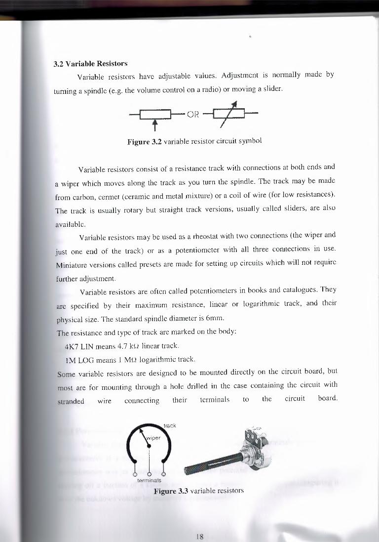
Variable resistors have adjustable values. Adjustment is normally made by
turning a spindle (e.g. the volume control on a radio) or moving a slider.
Figure 3.2 variable resistor circuit symbol
Variable resistors consist of a resistance track with connections at both ends and
a wiper which moves along the track as you tum the spindle. The track may be made
from carbon, cermet (ceramic and metal mixture) or a coil of wire (for low resistances).
The track is usually rotary but straight track versions, usually called sliders, are also
available. Variable resistors may be used as a rheostat with two connections (the wiper and
just one end of the track) or as a potentiometer with all three connections in use.
Miniature versions called presets are made for setting up circuits which will not require
further adjustment.
Variable resistors are often called potentiometers in books and catalogues. They
are specified by their maximum resistance, linear or logarithmic track, and their
physical size. The standard spindle diameter is 6mm.
The resistance and type of track are marked on the body:
4K7 LIN means 4.7 kn linear track.
1 M LOG means 1 Mn logarithmic track.
Some variable resistors are designed to be mounted directly on the circuit board, but
most are for mounting through a hole drilled in the case containing the circuit with
tranded wire connecting their terminals to the circuit board.
terminals
Figure 3.3 variable resistors
18

• Linear (LIN) and Logarithmic (LOG) tracks
Linear (LIN) track means that the resistance changes at a constant rate as you
move the wiper. This is the standard arrangement and you should assume this type is
required if a project does not specify the type of track. Presets always have linear tracks.
A linear pot has a resistive element of constant cross-section, resulting in a device
vhere the resistance between the wiper and one end terminal is proportional to the
distance between them. Linear describes the electrical 'law' of the device, not the
geometry of the resistive element.
• Logarithmic (LOG) track Logarithmic (LOG) track means that the resistance changes slowly at one end of
e track and rapidly at the other end, so halfway along the track is not half the total
sistance! This arrangement is used for volume (loudness) controls because the human
has a logarithmic response to loudness so fine control (slow change) is required at
.,· volumes and coarser control (rapid change) at high volumes. It is important to
nnect the ends of the track the correct way round, if you find that turning the spindle
eases the volume rapidly followed by little further change you should swap the
nnections to the ends of the track.
A Jog pot has a resistive element that either 'tapers' in from one end to the other,
made from a material whose resistivity varies from one end to the other. This
Its in a device where output voltage is a logarithmic ( or inverse logarithmic
nding on type) function of the mechanical angle of the pot.
Most (cheaper) "log" pots are actually not logarithmic, but use two regions of
ferent, but constant, resistivity to approximate a logarithmic law. A log pot can also
simulated with a linear pot and an external resistor. True log pots are significantly
re expensive.
I Potentiometer Variable resistors used as potentiometers have all three terminals connected. A
ntiometer is a variable resistor that functions as a voltage divider. Originally a
entiometer was an instrument to measure the potential (or voltage) in a circuit by
ing off a fraction of a known voltage from a resistive slide wire and comparing it
the unknown voltage by means of a galvanometer.
19
•
Figure 3.4 Potentiometer Symbol
The present popular usage of the term potentiometer (or 'pot' for short) describes
an electrical device which has a user-adjustable resistance. Usually, this is a three
terminal resistor with a sliding contact in the center (the wiper). If all three terminals are
used, it can act as a variable voltage divider. If only two terminals are used ( one side
and the wiper), it acts as a variable resistor. Its shortcoming is that of corrosion or
wearing of the sliding contact, especially if it is kept in one position.
Tlri~ {l[[fl!lgemeRl j!j ]}DJmaJJy used to vary voltage, for example to set the
witching point of a circuit with a sensor, or control the volume (loudness) in an
amplifier circuit. If the terminals at the ends of the track are connected across the power
supply then the wiper terminal will provide a voltage which can be varied from zero up
o the maximum of the supply.
• Potentiometer as electronic component
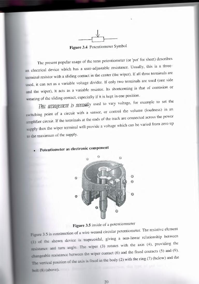
Figure 3.5 inside of a potentionmeter
Fisure 3.5 is construction of a wire-wound circular potentiometer. The resistive element
of the shown device is trapezoidal, giving a non-linear relationship between
isiance and turn angle. The wiper (3) rotates with the axis (4), providing the
=eable resistance between the wiper contact (6) and the fixed contacts (5) and (9).
-ertical position of the axis is fixed in the body (2) with the ring (7) (below) and the
above).
_o
•
In modem usage, a potentiometer is a potential divider, a three terminal resistor where
the position of the sliding connection is user adjustable via a knob or slider.
Potentiometers are sometimes provided with one or more switches mounted on
the same shaft. For instance, when attached to a volume control, the knob can also
function as an on/off switch at the lowest volume.
Ordinary potentiometers are rarely used to control anything of significant power
(even lighting) directly due to resistive losses, but they are frequently used to adjust the
level of analog signals (e.g. volume controls on audio equipment) and as control inputs
for electronic circuits ( e.g. a typical domestic light dimmer uses a potentiometer to set
the point in the cycle at which the triac turns on). Potentiometers used to control high
power are normally called rheostats.
• Low-power types A potentiometer is constructed using a flat graphite annulus as the resistive
element, with a sliding contact (wiper) sliding around this annulus. The wiper is
connected to an axle and, via another rotating contact, is brought out as the third
terminal. On panel pots, the wiper is usually the centre terminal. For single tum pots,
this wiper typically travels just under one revolution around the contact. 'Multitum'
potentiometers also exist, where the resistor element may be helical and the wiper may
move 10, 20, or more complete revolutions. In addition to graphite, other materials may
be used for the resistive element. These may be resistance wire or carbon particles in
plastic or a ceramic/metal mixture.
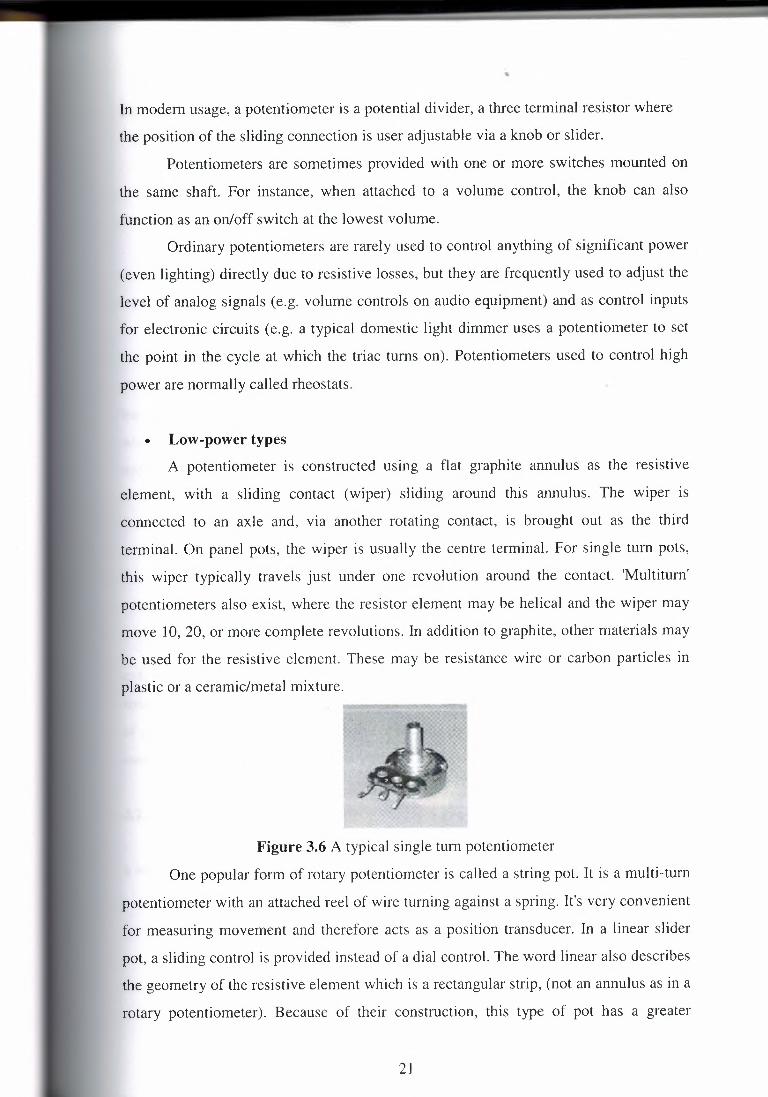
Figure 3.6 A typical single tum potentiometer
One popular form of rotary potentiometer is called a string pot. It is a multi-tum
potentiometer with an attached reel of wire turning against a spring. It's very convenient
for measuring movement and therefore acts as a position transducer. In a linear slider
pot, a sliding control is provided instead of a dial control. The word linear also describes
the geometry of the resistive element which is a rectangular strip, (not an annulus as in a
rotary potentiometer). Because of their construction, this type of pot has a greater
21

•
potential for getting contaminated. Potentiometers can be obtained with either linear or
logarithmic laws ( or "tapers").
Figure 3.7 PCB mount trimmer potentiometers or "trimpots" intended for infrequent
adjustment
• High-power types A rheostat is essentially a potentiometer, but is usually much larger, designed to
handle much higher voltage and current. Typically these are constructed as a resistive
wire wrapped to form a toroid coil (or most of one) with the wiper moving over the
upper surface of the toroid, sliding from one tum of the wire to the next.
Figure 3.8 A high power toroidal wirewound rheostat
Sometimes a rheostat is made from resistance wire wound on a heat resisting
cylinder with the slider made from a number of metal fingers that grip lightly onto a
small portion of the turns of resistance wire. The 'fingers' can be moved along the coil
of resistance wire by a sliding knob thus changing the 'tapping' point. They are usually
used as variable resistors rather than variable potential dividers.
3.2.2 Rheostat Rheostats are often used to vary current, for example to control the brightness of
a lamp or the rate at which a capacitor charges.
Figure 3.9 Rheostat Symbol
22

If the rheostat is mounted on a printed circuit board you may find that all three terminals
are connected! However, one of them will be linked to the wiper terminal. This
improves the mechanical strength of the mounting but it serves no function electrically.
3.2.3 Theory of operation of potentionmeter The 'modem' potentiometer can be used as a potential divider ( or voltage
divider) to obtain a manually adjustable output voltage at the slider (wiper) from a fixed
input voltage applied across the two ends of the pot. This is the simplest way of using a variable resistor. Two terminals are used: one
connected to an end of the track, the other to the moveable wiper. Turning the spindle
changes the resistance between the two terminals from zero up to the maximum
resistance.
Vs' R1
Vs\ '·r-;:r R2 I R2{ RL RL
Figure 3.10 A potentiometer with a resistive load, showing equivalent fixed resistors
for clarity.
This is the most common use of pots. The voltage across RL is determined by
the formula:
7 R2\\RL •
\. L = R1 + R2 II RL . \ s (3)
The parallel lines indicate components in parallel. Expanded fully, the equation
becomes: . R,RL . h = ----·-·· - -·-. ··--·- . \ ·,
RiRL + R2RL + R1R2 • (4)
Although it is not always the case, if RL is large compared to the other resistances, the
outpuj voltage can be approximated by the simpler equation:
1· = R2 . v, L r» + D · rc2
(5)
As an example, assume;
\:;, = 10 v R1 = 1 ld1, R2 = 2 kD, and RL = 100 kn Since the load resistance is large compared to the other resistances, the output voltage
VL will be approximately:
_3

•
2 kr-2 •) 1 l·O + .-, 1-1) . 10 V = :'.::. · 1D V ·::c.-: !'I Rfi~ \'
~,;i '-' 4. :\....: '-' :3 - '- •'- - [ I
Due to the load resistance, however, it will actually be slightly lowerr> 6.623 V.
One of the advantages of the potential divider compared to a variable resistor in series
with the source is that, while variable resistors have a maximum resistance where some
current will always flow, dividers are able to vary the output voltage from maximum
(VS) to ground (zero volts) as the wiper moves from one end of the pot to the other.
There is, however, always a small amount of contact resistance.
In addition, the load resistance is often not known and therefore simply placing a
variable resistor in series with the load could have a negligible effect or an excessive
effect, depending on the load.
3.2.4 Applications of potentiometers
Transducers
Potentiometers are also very widely used as a part of displacement transducers because
of the simplicity of construction and because they can give a large output signal.
• Audio control
Figure 3.11 Sliding potentiometers ("faders")
One of the most common uses for modem low-power potentiometers is as audio
control devices. Both sliding pots (also known as faders) and rotary potentiometers
(commonly called knobs) are regularly used to adjust loudness, frequency attenuation
and other characteristics of audio signals.
The 'log pot' is used as the volume control in audio amplifiers, where it is also
called 4n "audio taper pot", because the amplitude response of the human ear is also
logarithmic. It ensures that, on a volume control marked O to 10, for example, a setting
of 5 sounds half as loud as a setting of 10. There is also an anti-log pot or reverse audio
taper which is simply the reverse of a log pot. It is almost always used in a ganged
configuration with a log pot, for instance, in an audio balance control. A potentiometer
used in combination with an inductor or capacitor acts as a "tone" control.
24

CHAPTER 4. DIODES
4.1 Overview
Diode is two-terminal electronic device that permits current flow predominantly
in only one direction. Most diodes are semiconductor devices; diode electron tubes are
now used only for a few specialized applications. A diode has a low resistance to
electric current in one direction and a high resistance to it in the reverse direction. This
property makes a diode useful as a rectifier, which can convert alternating current (AC)
into direct current (DC). An arrangement of four diodes, called a diode bridge,
transforms AC into DC using both phases of the alternating current. When the voltage
applied in the reverse direction exceeds a certain value, a semiconductor diode "breaks
down" and conducts heavily in the direction of normally high resistance. When the
reverse voltage at which breakdown occurs remains nearly constant for a wide range of
currents, the phenomenon is called avalanching. A diode using this property, called a
Zener diode, can be used to regulate the voltage in a circuit.
A circuit element diode is said to rectify if voltage increments of equal
magnitude but opposite sign applied to the element produce unequal current increments.
An ideal rectifier diode is one that conducts fully in one direction (forward) and not at
all in the opposite direction (reverse). This property is approximated in junction and
thermionic diodes. Processes that make use of rectifier diodes include power
rectification, detection, modulation, and switching.
Negative-resistance diodes, which include tunnel and Gunn diodes, are used as
the basis of pulse generators, bistable counting and storage circuits, and oscillators.
Breakdown-diode current increases very rapidly with voltage above the
breakdown voltage; that is, the voltage is nearly independent of the current. In series
with resistance to limit the current to a nondestructive value, breakdown diodes can
therefore be used as a means of obtaining a nearly constant reference voltage or of
maintaining a constant potential difference between two circuit points, such as the
emitter and the base of a transistor. Breakdown diodes (or reverse-biased ordinary
junction diodes) can be used between two circuit points in order to limit alternating
voltage amplitude or to clip voltage peaks.
Light-sensitive diodes, which include phototubes, photovoltaic cells, photodiodes, and
photoconductive cells, are used in the measurement of illumination, in the control of
lights or other electrical devices by incident light, and in the conversion of radiant
25
energy into electrical energy. Light-emitting diodes (LEDs) are used in the display of
letters, numbers, and other symbols in calculators, watches, clocks, and other electronic
units.
,1
l ,, '.'!,~
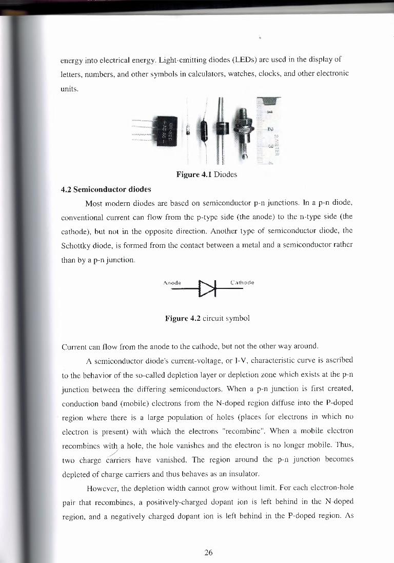
Figure 4.1 Diodes
4.2 Semiconductor diodes Most modem diodes are based on semiconductor p-n junctions. In a p-n diode,
conventional current can flow from the p-type side (the anode) to the n-type side (the
cathode), but not in the opposite direction. Another type of semiconductor diode, the
Schottky diode, is formed from the contact between a metal and a semiconductor rather
than by a p-n junction.
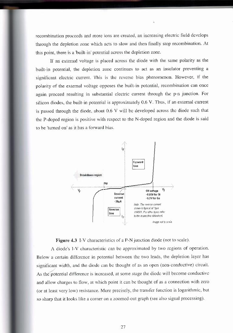
----1(::i Carh o de .1\node
Figure 4.2 circuit symbol
Current can flow from the anode to the cathode, but not the other way around.
A semiconductor diode's current-voltage, or I-V, characteristic curve is ascribed
to the behavior of the so-called depletion layer or depletion zone which exists at the p-n
junction between the differing semiconductors. When a p-n junction is first created,
conduction band (mobile) electrons from the N-doped region diffuse into the P-doped
region where there is a large population of holes (places for electrons in which no
electron is present) with which the electrons "recombine". When a mobile electron
recombines w,, a hole, the hole vanishes and the electron is no longer mobile. Thus,
two charge carriers have vanished. The region around the p-n junction becomes
depleted of charge carriers and thus behaves as an insulator.
However, the depletion width cannot grow without limit. For each electron-hole
pair that recombines, a positively-charged dopant ion is left behind in the N-doped
region, and a negatively charged dopant ion is left behind in the P-doped region. As
26
•
recombination proceeds and more ions are created, an increasing electric field develops
through the depletion zone which acts to slow and then finally stop recombination. At
this point, there is a 'built-in' potential across the depletion zone.
If an external voltage is placed across the diode with the same polarity as the
built-in potential, the depletion zone continues to act as an insulator preventing a
significant electric current. This is the reverse bias phenomenon. However, if the
polarity of the external voltage opposes the built-in potential, recombination can once
again proceed resulting in substantial electric current through the p-n junction. For
silicon diodes, the built-in potential is approximately 0.6 V. Thus, if an external current
is passed through the diode, about 0.6 V will be developed across the diode such that
the P-doped region is positive with respect to the N-doped region and the diode is said
to be 'turned on' as it has a forward bias.
forward bias
Breakd.o~n·regi~n
, PIV ; -1 '\ ,;.., -· ,,_,,,_, __ t-·-·-· ~-·-·- ····t -- ·----7 -, v, /_. /t OIi voltage v, '
Reverse I "0.65V for Si current ! -0.2V for Ge -30fl.A !
' I lrt t \l/
Note: The reverse current shown is /!;pica! of ti;pe 1N4001. For other /ljpes refer lo the respective dalasheel.
Image not to scale
Figure 4.3 I-V characteristics of a P-N junction diode (not to scale).
A diode's I-V characteristic can be approximated by two regions of operation.
Below a ce1tain difference in potential between the two leads, the depletion layer has
significant width, and the diode can be thought of as an open (non-conductive) circuit.
As the{otential difference is increased, at some stage the diode will become conductive
and allow charges to flow, at which point it can be thought of as a connection with zero
(or at least very low) resistance. More precisely, the transfer function is logarithmic, but
so sharp that it looks like a comer on a zoomed-out graph (see also signal processing).
27
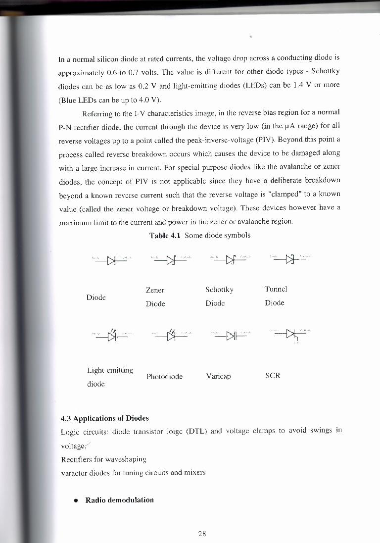
In a normal silicon diode at rated currents, the voltage drop across a conducting diode is
approximately 0.6 to 0.7 volts. The value is different for other diode types - Schottky
diodes can be as low as 0.2 V and light-emitting diodes (LEDs) can be 1.4 V or more
(Blue LEDs can be up to 4.0 V). Referring to the 1-V characteristics image, in the reverse bias region for a normal
P-N rectifier diode, the current through the device is very low (in the µA range) for all
reverse voltages up to a point called the peak-inverse-voltage (PIV). Beyond this point a
process called reverse breakdown occurs which causes the device to be damaged along
with a large increase in current. For special purpose diodes like the avalanche or zener
diodes, the concept of PIV is not applicable since they have a deliberate breakdown
beyond a known reverse current such that the reverse voltage is "clamped" to a known
value (called the zener voltage or breakdown voltage). These devices however have a
maximum limit to the current and power in the zener or avalanche region.
Table 4.1 Some diode symbols
'"~··'·· ,,.,;, l'-.J'1 ' ..• , . ~,,y,
Diode Zener
Diode
Schottky
Diode
Tunnel
Diode
Light-emitting
diode Photodiode Varicap SCR
4.3 Applications of Diodes Logic circuits: diode transistor loigc (DTL) and voltage clamps to avoid swmgs in
voltage>"
Rectifiers for waveshaping
varactor diodes for tuning circuits and mixers
• Radio demodulation
28

•
The first use for the diode was the demodulation of amplitude modulated (AM)
radio broadcasts. In summary, an AM signal consists of alternating positive and
negative peaks of voltage, whose amplitude or 'envelope' is proportional to the original
audio signal, but whose average value is zero. The diode (originally a crystal diode)
rectifies the AM signal, leaving a signal whose average amplitude is the desired audio
signal. The average value is extracted using a simple filter and fed into an audio
transducer, which generates sound.
• Power conversion Rectifiers are constructed from diodes, where they are used to convert
alternating current (AC) electricity into direct current (DC). Similarly, diodes are also
used in Cockcroft-Walton voltage multipliers to convert AC into very high DC voltages.
• Over-voltage protection Diodes are frequently used to conduct damaging high voltages away from
sensitive electronic devices. They are usually reverse-biased (non-conducting) under
normal circumstances, and become forward-biased ( conducting) when the voltage rises
above its normal value. For example, diodes are used in stepper motor and relay circuits
to de-energize coils rapidly without the damaging voltage spikes that would otherwise
occur. Many integrated circuits also incorporate diodes on the connection pins to
prevent external voltages from damaging their sensitive transistors. Specialized diodes
are used to protect from over-voltages at higher power.
• Logic gates Diodes can be combined with other components to construct AND and OR logic
gates. This is referred to as diode logic.
• Temperature measuring A diode can be used as a temperature measuring device, since the forward
voltage drop across the diode depends on temperature. This temperature dependence
follows from the Shockley ideal diode equation given above and is typically around -2.2
m V per degree Celsius.
e-----Charge coupled devices Digital cameras and similar units use arrays of photo diodes, integrated with
readout circuitry.
29
•
CHAPTER 5. LED
5.1. Overview Led is a semiconductor diode that converts electric energy into electromagnetic
radiation at a visible and near infrared frequencies when its pn junction is forward
biased. A light-emitting diode (LED) is a semiconductor device that emits incoherent
narrow-spectrum light when electrically biased in the forward direction of the p-n
junction. This effect is a form of electroluminescence. An LED is a small extended
source with extra optics added to the chip that makes an LED to emit a complex
radiation pattern. The color of the emitted light depends on the composition and
condition of the semiconducting material used, and can be infrared, visible or near-
ultraviolet.
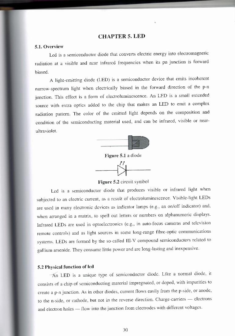
Figure 5.1 a diode
Figure 5.2 circuit symbol
Led is a semiconductor diode that produces visible or infrared light when
subjected to an electric current, as a result of electroluminescence. Visible-light LEDs
are used in many electronic devices as indicator lamps (e.g., an on/off indicator) and,
when arranged in a matrix, to spell out letters or numbers on alphanumeric displays.
Infrared LEDs are used in optoelectronics (e.g., in auto-focus cameras and television
remote controls) and as light sources in some long-range fibre-optic communications
systems. LEDs are formed by the so-called lll-V compound semiconductors related to
gallium arsenide. They consume little power and are long-lasting and inexpensive.
5.2 Physical function of led ~ LED is a unique type of semiconductor diode. Like a normal diode, it
consists of a chip of semiconducting material impregnated, or doped, with impurities to
create a p-n junction. As in other diodes, current flows easily from the p-side, or anode,
to the n-side, or cathode, but not in the reverse direction. Charge-carriers - electrons
and electron holes - flow into the junction from electrodes with different voltages.
30
When an electron meets a hole, it falls into a lower energy level, and releases
energy in the form of a photon.
The wavelength of the light emitted, and therefore its color, depends on the band
gap energy of the materials forming the p-n junction. In silicon or germanium diodes,
the electrons and holes recombine by a non-radiative transition which produces no
optical emission, because these are indirect bandgap materials. The materials used for
an LED have a direct band gap with energies corresponding to near-infrared, visible or
near-ultraviolet light.
LEDs are usually constantly illuminated when a current passes through them,
but flashing LEDs are also available. Flashing LEDs resemble standard LEDs but they
contain a small chip inside which causes the LED to flash with a typical period of one
second. This type of LED comes most commonly as red, yellow, or green. Most
flashing LEDs emit light of a single wavelength, but multicolored flashing LEDs are
available too.
LED development began with infrared and red devices made with gallium
arsenide. Advances in materials science have made possible the production of devices
with ever-shorter wavelengths, producing light in a variety of colors.
LEDs are usually built on an n-type substrate, with electrode attached to the p
type layer deposited on its surface. P-type substrates, while less common, occur as well.
Many commercial LEDs, especially GaN/InGaN, also use sapphire substrate. Substrates
that are transparent to the emitted wavelength, and backed by a reflective layer, increase
the LED efficiency. The refractive index of the package material should match the index
of the semiconductor, otherwise the produced light gets partially reflected back into the
semiconductor, where it gets absorbed and turns into additional heat.
The semiconducting chip is encased in a solid plastic lens, which is much
tougher than the glass envelope of a traditional light bulb or tube. The plastic may be
colored, but this is only for cosmetic reasons or to improve the contrast ratio; the color
of the packaging does not substantially affect the color of the light emitted.
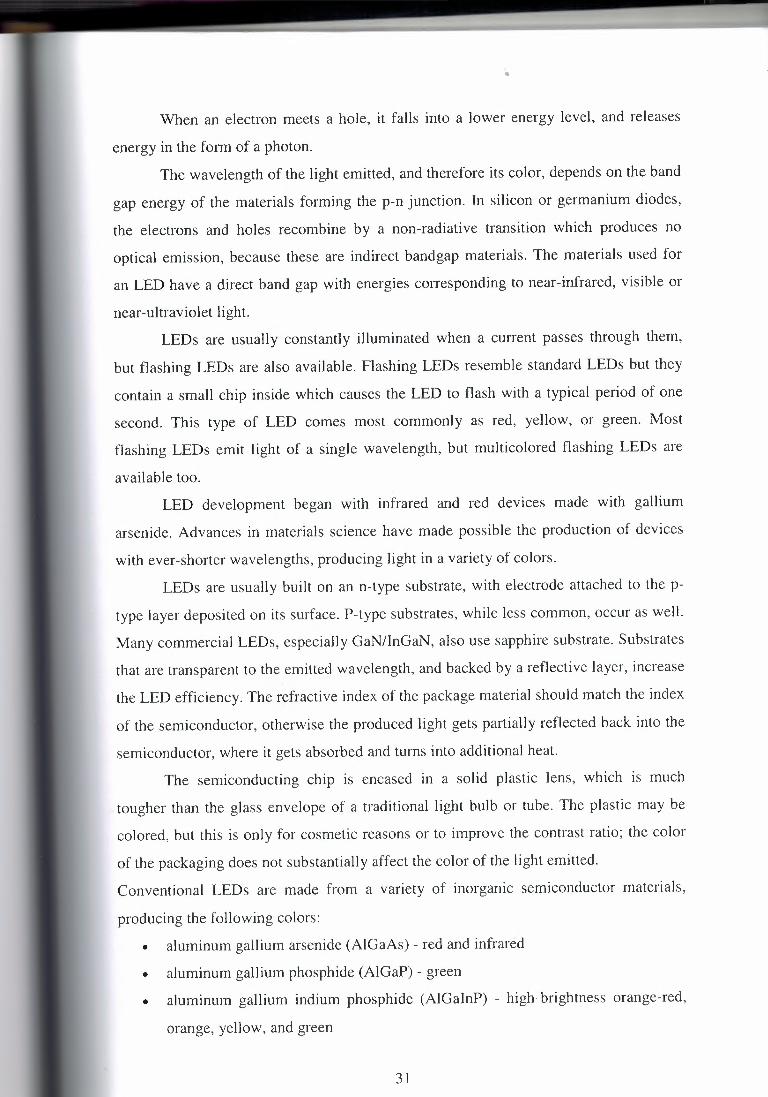
Conventional LEDs are made from a variety of inorganic semiconductor materials,
producing the following colors:
• aluminum gallium arsenide (AlGaAs) - red and infrared
• aluminum gallium phosphide (AlGaP) - green
• aluminum gallium indium phosphide (AlGalnP) - high-brightness orange-red,
orange, yellow, and green
31

• gallium arsenide phosphide (GaAsP) - red, orange-red, orange, and yellow
• gallium phosphide (GaP) - red, yellow and green
• gallium nitride (GaN) - green, pure green (or emerald green), and blue also
white (if it has an AIGaN Quantum Barrier)
• indium gallium nitride (lnGaN) - near ultraviolet, bluish-green and blue
• silicon carbide (SiC) as substrate - blue
• silicon (Si) as substrate - blue (under development)
• sapphire (Al203) as substrate - blue
• zinc selenide (ZnSe) - blue
• diamond (C) - ultraviolet
• aluminum nitride (AIN), aluminum gallium nitride (AIGaN) - near to far
ultraviolet (down to 210 nm[4])
5.3 What is Inside an LED? LED's are special diodes that emit light when connected in a circuit. They are
frequently used as "pilot" lights in electronic appliances to indicate whether the circuit
is closed or not. A a clear (or often colored) epoxy case enclosed the heart of an LED,
the semi-conductor chip.
LED leads
<-- -->
side lead on flat
+ side of bulb = negative
Figure 5.3 diode leads
The two wires extending below the LED epoxy enclosure, or the "bulb" indicate
how the LED should be connected into a circuit. The negative side of an LED lead is
indicated in two ways: 1) by the flat side of the bulb, and 2) by the shorter of the two
wires extending from the LED. The negative lead should be connected to the negative
terminal of a battery. LED's operate at relative low voltages between about 1 and 4
volts, and draw currents between about 10 and 40 milliamperes. Voltages and currents
substantially above these values can melt a LED chip.
32

•
The most important part of a light emitting diode (LED) is the semi-conductor
chip located in the center of the bulb as shown at the right. The chip has two regions
separated by a junction. The p region is dominated by positive electric charges, and the
n region is dominated by negative electric charges. The junction acts as a barrier to the
flow of electrons between the p and the n regions. Only when sufficient voltage is
applied to the semi-conductor chip, can the current flow, and the electrons cross the
junction into the p region. In the absence of a large enough electric potential difference
(voltage) across the LED leads, the junction presents an electric potential barrier to the
flow of electrons.
5.4 What Causes the LED to Emit Light and What Determines the Color of the
Light? When sufficient voltage is applied to the chip across the leads of the LED,
electrons can move easily in only one direction across the junction between the p and n
regions. In the p region there are many more positive than negative charges. In the n
region the electrons are more numerous than the positive electric charges. When a
voltage is applied and the current starts to flow, electrons in the n region have sufficient
energy to move across the junction into the p region. Once in the p region the electrons
are immediately attracted to the positive charges due to the mutual Coulomb forces of
attraction between opposite electric charges. When an electron moves sufficiently close
to a positive charge in the p region, the two charges "re-combine".
Each time an electron recombines with a positive charge, electric potential energy is
converted into electromagnetic energy. For each recombination of a negative and a
positive charge, a quantum of electromagnetic energy is emitted in the form of a photon
of light with a frequency characteristic of the semi-conductor material (usually a
combination of the chemical elements gallium, arsenic and phosphorus). Only photons
in a very narrow frequency range can be emitted by any material. LED's that emit
different colors are made of different semi-conductor materials, and require different
energies to light them.
In the absence of a large enough electric potential difference (voltage) across the
LED leads, the junction presents an electric potential barrier to the flow of electrons.
5.5 How Much Energy Does an LED Emit?
33

•
The electric energy is proportional to the voltage needed to cause electrons to
flow across the p-n junction. The different colored LED's emit predominantly light of a
single color. The energy (E) of the light emitted by an LED is related to the electric
charge ( q) of an electron and the voltage (V) required to light the LED by the
expression: E = qV Joules. This expression simply says that the voltage is proportional
to the electric energy, and is a general statement which applies to any circuit, as well as
to LED's. The constant q is the electric charge of a single electron, -1.6 x 10⁻¹⁹
Coulomb.
5.6 LED applications
• Architectural lighting
• Status indicators on all sorts of equipment
• Traffic lights and signals
• Exit signs
• Motorcycle and Bicycle lights
• Toys and recreational sporting goods, such as the Flashflight
• Railroad crossing signals
• Continuity indicators
• Flashlights. Some models that do not even use batteries are of this type.
• Light bars on emergency vehicles.
• Elevator Push Button Lighting
• Thin, lightweight message displays at airports and railway stations and as
destination displays for trains, buses, trams and ferries.
• Red or yellow LEDs are used in indicator and alphanumeric displays in
environments where night vision must be retained: aircraft cockpits, submarine
and ship bridges, astronomy observatories, and in the field, e.g. night time
animal watching and military field use.
• Red, yellow, green, and blue LEDs can be used for model railroading
applications
• Remote controls, such as for TVs and VCRs, often use infrared LEDs.
• In optical fiber and Free Space Optics communications.
• In dot matrix arrangements for displaying messages.
• Glowlights, as a more expensive but longer lasting and reusable alternative to
Glowsticks.
34

• Movement sensors, for example in optical computer mice
• Because of their long life and fast switching times, LEDs have been used for
automotive high-mounted brake lights and truck and bus brake lights and tum
signals for some time, but many high-end vehicles are now starting to use LEDs
for their entire rear light clusters. Besides the gain in reliability, this has styling
advantages because LEDs are capable of forming much thinner lights than
incandescent lamps with parabolic reflectors. The significant improvement in
the time taken to light up (perhaps 0.5s faster than an incandescent bulb)
improves safety by giving drivers more time to react.
• Backlighting for LCD televisions and displays. The availability of LEDs in
specific colors (RGB) enables a full-spectrum light source which expands the
color gamut by as much as 45%.
• New stage lighting equipment is being developed with LED sources in primary
red-green-blue arrangements.
• Lumalive, a photonic textile
• As Voltage Reference in electronic circuits. The constant voltage drop (e.g. 1.7
V for a normal red LED) can be used instead of a Zener diode in low-voltage
regulators. Zener diodes are not available below voltages of about 3 V.
5.7 Illumination applications of LED LEDs used as a replacement for incandescent light bulbs and fluorescent lamps
are known as solid-state lighting (SSL) - packaged as a cluster of white LEDs grouped
together to form a light source (pictured). LEDs are moderately efficient; the average
commercial SSL currently outputs 32 lumens per watt (Jm/W), and new technologies
promise to deliver up to 80 lm/W. The long lifetime of LEDs make SSL very attractive.
They are also more mechanically robust than incandescent light bulbs and fluorescent
tubes. Currently, solid state lighting is becoming more available for household use but is
relatively expensive, although costs are decreasing. LED flashlights, however, already
have become widely available. Recently a number of manufacturers have started
marketing ultra-compact LCD video projectors that use high-powered white LEDS for
the light source. Incandescent bulbs are much less expensive but also less efficient,
generating from about 16 lm/W for a domestic tungsten bulb to 22 lm/W for a halogen
bulb. Fluorescent tubes are more efficient, providing 50 to 100 lm/W for domestic tubes
(average 60 lm/W), but are bulky and fragile and require starter or ballast circuits that
35
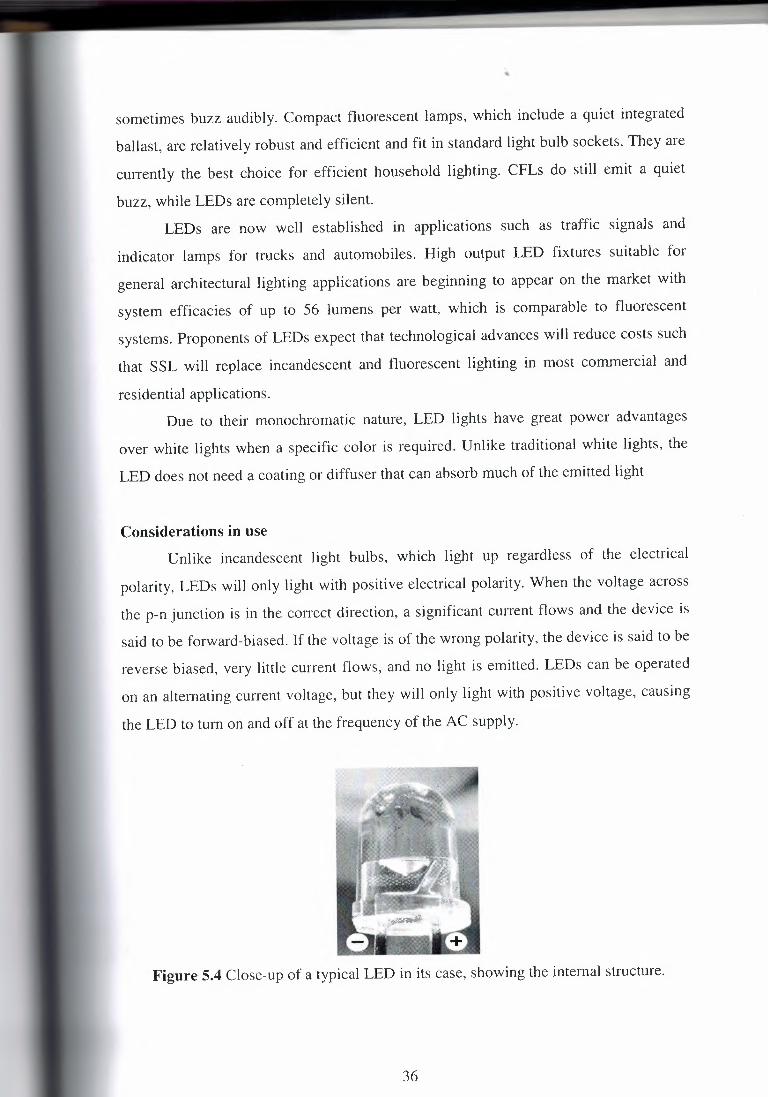
•
sometimes buzz audibly. Compact fluorescent lamps, which include a quiet integrated
ballast, are relatively robust and efficient and fit in standard light bulb sockets. They are
currently the best choice for efficient household lighting. CFLs do still emit a quiet
buzz, while LEDs are completely silent.
LEDs are now well established in applications such as traffic signals and
indicator lamps for trucks and automobiles. High output LED fixtures suitable for
general architectural lighting applications are beginning to appear on the market with
system efficacies of up to 56 lumens per watt, which is comparable to fluorescent
systems. Proponents of LEDs expect that technological advances will reduce costs such
that SSL will replace incandescent and fluorescent lighting in most commercial and
residential applications.
Due to their monochromatic nature, LED lights have great power advantages
over white lights when a specific color is required. Unlike traditional white lights, the
LED does not need a coating or diffuser that can absorb much of the emitted light
Considerations in use Unlike incandescent light bulbs, which light up regardless of the electrical
polarity, LEDs will only light with positive electrical polarity. When the voltage across
the p-n junction is in the correct direction, a significant current flows and the device is
said to be forward-biased. If the voltage is of the wrong polarity, the device is said to be
reverse biased, very little current flows, and no light is emitted. LEDs can be operated
on an alternating current voltage, but they will only light with positive voltage, causing
the LED to tum on and off at the frequency of the AC supply.
Figure 5.4 Close-up of a typical LED in its case, showing the internal structure.
36
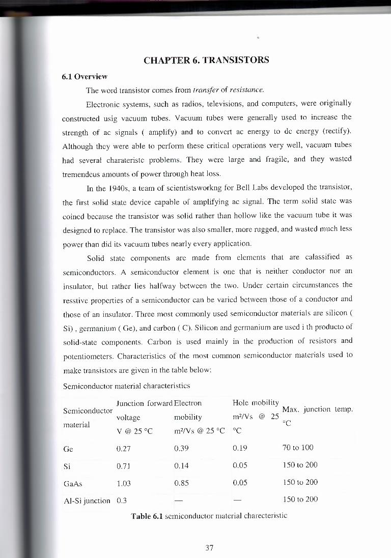
CHAPTER 6. TRANSISTORS
6.1 Overview The word transistor comes from transfer of resistance.
Electronic systems, such as radios, televisions, and computers, were originally
constructed usig vacuum tubes. Vacuum tubes were generally used to increase the
strength of ac signals ( amplify) and to convert ac energy to de energy (rectify).
Although they were able to perform these critical operations very well, vacuum tubes
had several charateristc problems. They were large and fragile, and they wasted
tremendeus amounts of power through heat loss.
In the 1940s, a team of scientistsworkng for Bell Labs developed the transistor,
the first solid state device capable of amplifying ac signal. The term solid state was
coined because the transistor was solid rather than hollow like the vacuum tube it was
designed to replace. The transistor was also smaller, more rugged, and wasted much less
power than did its vacuum tubes nearly every application.
Solid state components are made from elements that are calassified as
semiconductors. A semiconductor element is one that is neither conductor nor an
insulator, but rather lies halfway between the two. Under certain circumstances the
resstive properties of a semiconductor can be varied between those of a conductor and
those of an insulator. Three most commonly used semiconductor materials are silicon (
Si), germanium ( Ge), and carbon ( C). Silicon and germanium are used i th producto of
solid-state components. Carbon is used mainly in the production of resistors and
potentiometers. Characteristics of the most common semiconductor materials used to
make transistors are given in the table below:
Semiconductor material characteristics
Junction forward Electron Hole mobility Semiconductor Max. junction temp.
voltage mobility m2/Vs @ 25 material oc
V@ 25 °C m2/Vs@ 25 °C oc
Ge 0.27 0.39 0.19 70 to 100
Si 0.71 0.14 0.05 150 to 200
GaAs 1.03 0.85 0.05 150 to 200
Al-Si junction 0.3 150 to 200
Table 6.1 semiconductor material charecteristic
37

Figure 6.1 Assorted discrete transistors
A transistor is a semiconductor device, commonly used as an amplifier. The
transistor is the fundamental building block of the circuitry that governs the operation of
computers, cellular phones, and all other modem electronics. A transistor is an
electronic component used in a circuit to control a large amount of current or voltage
with a small amount of voltage or current. The transistor is a three-terminal device
whose output current, voltage, and\or power are controlled by its input. In digital
systems, the transistor is used as a high speed electronic switch capable of switching
between two operating states (open and closed) at a rate of several bilions of times per
second.
Because of its fast response and accuracy, the transistor may be used in a wide
variety of digital and analog functions, including amplification, switching, voltage
regulation, signal modulation, and oscillators. Transistors may be packaged individually
or as part of an integrated circuit chip, which may hold thousands of transistors in a very
small area.
The transistors consisted of a thin germanium wafer connected to two extremely
thin wires. The wires are spaced only a few thousands of an inch part. A current
introduced to one of the wires was amplified by the germanium wafer, and the larger
output current was taken from the other wire.
How do transistors work? Transistors work on the principle that certain materials e.g. silicon, can after
processing be made to perform as "solid state" devices. Any material is only conductive
in proportion to the number of "free" electrons that are available. Silicon crystals for
example have very few free electrons. However if "impurities" (different atomic
structure - e.g. arsenic) are introduced in a controlled manner then the free electrons or
conductivity is increased. By adding other impurities such as gallium, an electron
deficiency or hole is created. As with free electrons, the holes also encourage
38
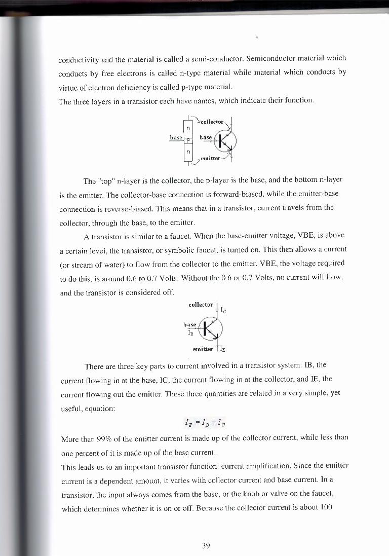
•
conductivity and the material is called a semi-conductor. Semiconductor material which
conducts by free electrons is called n-type material while material which conducts by
virtue of electron deficiency is called p-type material.
The three layers in a transistor each have names, which indicate their function.
The "top" n-layer is the collector, the p-layer is the base, and the bottom n-layer
is the emitter. The collector-base connection is forward-biased, while the emitter-base
connection is reverse-biased. This means that in a transistor, current travels from the
collector, through the base, to the emitter.
A transistor is similar to a faucet. When the base-emitter voltage, VBE, is above
a certain level, the transistor, or symbolic faucet, is turned on. This then allows a current
(or stream of water) to flow from the collector to the emitter. VBE, the voltage required
to do this, is around 0.6 to 0.7 Volts. Without the 0.6 or 0.7 Volts, no current will flow,
and the transistor is considered off. collector
There are three key parts to current involved in a transistor system: IB, the
current flowing in at the base, IC, the current flowing in at the collector, and IE, the
cunent flowing out the emitter. These three quantities are related in a very simple, yet
useful, equation:
IE=le+lc
More than 99% of the emitter current is made up of the collector current, while less than
one percent of it is made up of the base current,
This leads us to an important transistor function: current amplification. Since the emitter
cunent is a dependent amount, it varies with collector current and base current, In a
transistor, the input always comes from the base, or the knob or valve on the faucet,
which determines whether it is on or off. Because the collector current is about 100
39
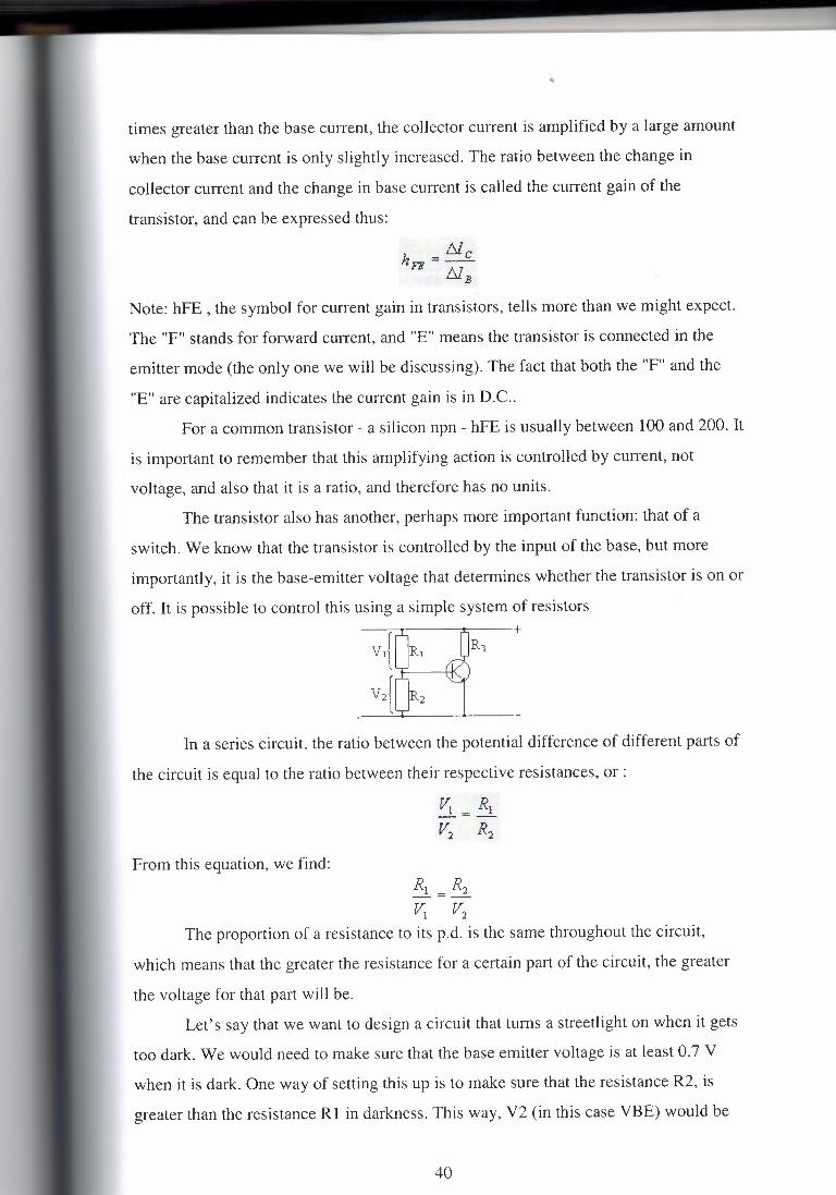
•
times greater than the base current, the collector current is amplified by a large amount
when the base current is only slightly increased. The ratio between the change in
collector current and the change in base current is called the current gain of the
transistor, and can be expressed thus:
h = Ne . FE
NB
Note: hFE , the symbol for current gain in transistors, tells more than we might expect.
The "F" stands for forward current, and "E" means the transistor is connected in the
emitter mode (the only one we will be discussing). The fact that both the "F" and the
"E" are capitalized indicates the current gain is in D.C..
For a common transistor - a silicon npn - hFE is usually between 100 and 200. It
is important to remember that this amplifying action is controlled by current, not
voltage, and also that it is a ratio, and therefore has no units.
The transistor also has another, perhaps more important function: that of a
switch. We know that the transistor is controlled by the input of the base, but more
importantly, it is the base-emitter voltage that determines whether the transistor is on or
off. It is possible to control this using a simple system of resistors
In a series circuit, the ratio between the potential difference of different parts of
the circuit is equal to the ratio between their respective resistances, or :
fr~ = R1
V2 R2
From this equation, we find: R1 = R2 v~ v2
The proportion of a resistance to its p.d. is the same throughout the circuit,
which means that the greater the resistance for a certain part of the circuit, the greater
the voltage for that part will be.
Let's say that we want to design a circuit that turns a streetlight on when it gets
too dark. We would need to make sure that the base emitter voltage is at least 0.7 V
when it is dark. One way of setting this up is to make sure that the resistance R2, is
greater than the resistance Rl in darkness. This way, V2 (in this case VBE) would be
40

•
greater than Vl. Since only 0.7 Volts are required to tum on the transistor, it is therefore
almost certain that whenever V2 > V 1, the transistor will tum on.
However, in order not to waste electricity, we would want to make sure that the
streetlight is not on during the day as well. This means that while it is light out, Rl
needs to be greater than R2 in such a proportion that V2 coulds not possibly reach 0.7
V. A resistor that changes its resistance with light would be needed to detect the point at
which the streetlight should go on. Since Light Dependent Resistors (LDR's) usually
increase their resistance as it gets darker, we would want an LDR to be R2. But we
definitely want to be able to decide at which point the streetlights should go on, which
means deciding at which point R2 should become greater than R 1. We can do this by
using a variable resistor, which will allow us to set a specific resistance for Rl. We
should set the resistance of Rl just under the resistance of R2 when it is in darkness.
When R2 allows V2 to be high enough, current can pass through R3 to activate
whatever result is desired, in this case, the streetlights.
Similar switch functions can be set up using other forms of resistors, such as a
water-detecting device for a sprinkler system. Devices like these, that convert a non
electrical signal into an electrical one are called transducers. Another example is a
motion sensor that can send a signal (via a transistor) to start a burglar alarm.
How do holes and electrons conduct in transistors? If we take a piece of the p-type material and connect it to a piece of n-type
material and apply voltage as in figure 6.2, then current will flow. Electrons will be
attracted across the junction of the p and n materials. Current flows by means of
electrons going one way and holes going in the other direction. If the battery polarity
were reversed then current flow would cease. current
Pl . ++++++
N -_-_-_-_-_._-
Figure 6.2 - electron flow in a p-n juction of a diode
Some very interesting points emerge here. As depicted in figure 1 above a
junction of p and n types constitutes a rectifier diode. Indeed a transistor can be
configured as a diode and often are in certain projects, especially to adjust for thermal
variations. Another behaviour which is often a limitation and at other times an asset is
41
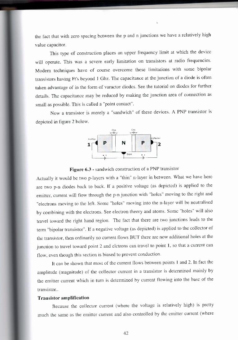
the fact that with zero spacing between the p and n junctions we have a relatively high
value capacitor.
This type of construction places an upper frequency limit at which the device
will operate. This was a severe early limitation on transistors at radio frequencies.
Modem techniques have of course overcome these limitations with some bipolar
transistors having Ft's beyond 1 Ghz. The capacitance at the junction of a diode is often
taken advantage of in the form of varactor diodes. See the tutorial on diodes for further
details. The capacitance may be reduced by making the junction area of connection as
small as possible. This is called a "point contact".
Now a transistor is merely a "sandwich" of these devices. A PNP transistor is
depicted in figure 2 below.
Cbe Cbc
+ I Base
Figure 6.3 - sandwich construction of a PNP transistor
Actually it would be two p-layers with a "thin" n-layer in between. What we have here
are two p-n diodes back to back. If a positive voltage (as depicted) is applied to the
emitter, current will flow through the p-n junction with "holes" moving to the right and
"electrons moving to the left. Some "holes" moving into then-layer will be neutralised
by combining with the electrons. See electron theory and atoms. Some "holes" will also
travel toward the right hand region. The fact that there are two junctions leads to the
term "bipolar transistor". If a negative voltage (as depicted) is applied to the collector of
the transistor, then ordinarily no current flows BUT there are now additional holes at the
junction to travel toward point 2 and elctrons can travel to point 1, so that a current can
flow, even though this section is biased to prevent conduction.
It can be shown that most of the current flows between points 1 and 2. In fact the
amplitude (magnitude) of the collector current in a transistor is determined mainly by
the emitter current which in tum is determined by current flowing into the base of the
transistor ..
Transistor amplification Because the collector current (where the voltage is relatively high) is pretty
much the same as the emitter current and also controlled by the emitter current (where
42

•
the voltage is usually much lower) it can be shown by ohms law P = I 2 * R that
amplification occurs.
Rules for Bias Connections
The Emitter - Base connection is always FORWARD biased. This means more
Positive to P type & more Negative to N type. Also, for a Silicon transistor, there must
be at least a 0.7 Volt DC bias across the emitter-base junction in order for the transistor
to be active. Of course, the bias is 0.3 Volts DC for Germanium Transistors.
The Collector - Base connection is always REVERSE biased. This means more Positive
goes to N type & more Negative goes to P type.
6.2 Importance The transistor's low cost, flexibility and reliability have made it a universal
device for non-mechanical tasks, such as digital computing. Transistorized circuits have
replaced electromechanical devices for the control of appliances and machinery as well.
It is often less expensive and more effective to use a standard microcontroller and write
a computer program to carry out a control function than to design an equivalent
mechanical control function.
6.3 Types of Transistors Modem transistors are divided into two main categories: bipolar junction
transistors (BJTs) and field effect transistors (FETs). The transistor characteristics
depend on their type.
N-channel
PNP P-channel
NPN
BJT JFET
Table 6.2 BJT and JFET symbols
Transistors are categorized by:
43

• Semiconductor material: germanium, silicon, gallium arsenide, silicon carbide
• Structure: BJT, JFET, IGFET (MOSFET), IGBT, "other types"
• Polarity: NPN, PNP (BJTs); N-channel, P-channel (FETs)
• Maximum power rating: low, medium, high
• Maximum operating frequency: low, medium, high, radio frequency (RF),
microwave (The maximum effective frequency of a transistor is denoted by the
term IT, an abbreviation for "frequency of transition". The frequency of
transition is the frequency at which the transistor yields unity gain).
• Application: switch, general purpose, audio, high voltage, super-beta, matched
pair
• Physical packaging: through hole metal, through hole plastic, surface mount,
ball grid array, power modules
PNP and NPN Transistors The most common type of transistor is called bipolar and these are divided into
NPN and PNP types. Today both are typically made by double-fission process that
involves the deposition of two additional layers of doped silicon on a doped silicon
wafer.
Their construction-material is most commonly silicon (their marking has the
letter B) or germanium (their marking has the letter A). Original transistor were made
from germanium, but they were very temperature-sensitive. Silicon transistors are much
more temperature-tolerant and much cheaper to manufacture.
The only differences between PNP and NPN transistors are in manufacturing
(i.e. location of the p-layers and n-layers) and of much importance in the biasing. The
schematic symbols for PNP and NPN transistors, (the work horse is the NPN) are
shown in figure 3 below. A silicon NPN transistor needs to be forward biased by about
0.65V for it to turn on.
The only functional difference between a PNP transistor and an NPN transistor is
the proper biasing (polarity) of the junctions when operating. For any given state of
operation, the cmTent directions and voltage polarities for each type of transistor are
exactly opposite each other.
• Bipolar junction transistor
44

The bipolar junction transistor (BJT) was the first type of transistor to be mass
produced. Bipolar transistors are so named because they conduct by using both majority
and minority carriers. The three terminals of the BJT are named emitter, base and
collector. Two p-n junctions exist inside a BJT: the base/emitter junction and
base/collector junction. The BJT is commonly described as a current-operated device
because the collector/emitter current is controlled by the current flowing between base
and emitter terminals. Unlike the FET, the BJT is a low input-impedance device. As the
base/emitter voltage (Vbe) is increased the base/emitter current and hence the
collector/emitter current (Ice) increase exponentially. Because of this exponential
relationship the BJT has a higher transconductance than the FET.
Bipolar transistors work as current-controlled current regulators. In other words,
they restrict the amount of current that can go through them according to a smaller,
controlling current. The main current that is controlled goes from collector to emitter, or
from emitter to collector, depending on the type of transistor it is (PNP or NPN,
respectively). The small current that controls the main current goes from base to emitter,
or from emitter to base, once again depending on the type of transistor it is (PNP or
NPN, respectively). According to the confusing standards of semiconductor symbology,
the arrow always points against the direction of electron flow:
T C
E
TIT ---;> = small, controlling current
~=large, controlled current
Figure 6.4 npn and pnp structure
Bipolar transistors are called bipolar because the main flow of electrons through them
takes place in two types of semiconductor material: P and N, as the main current goes
from emitter to collector ( or visa-versa). In other words, two types of charge carriers -
electrons anlf there is no current through the base of the transistor, it shuts off like an
open switch and prevents current through the collector. If there is a base current, then
the transistor turns on like a closed switch and allows a proportional amount of current
through the collector. Collector current is primarily limited by the base current,
45

•
regardless of the amount of voltage available to push it.d holes -- comprise this main
current through the transistor.
• Field-effect transistor The bipolar jnction transistor is a current controlled device, that is the output
transistor or FET is a voltage controlled device. The output characteristic of a FET are
controlled by the input voltage, not by the input current.
The field-effect transistor (FET), sometimes called a unipolar transistor, uses either
electrons (N-channel FET) or holes (P-channel FET) for conduction. The four terminals
of the FET are named source, gate, drain, and body (substrate). On most FETs the body
is connected to the source inside the package and this will be assumed for the following
description.
A voltage applied between the gate and source (body) controls the current flowing
between the drain and source. As the gate/source voltage (V gs) is increased the
drain/source current (Ids) increases roughly parabolically (Ids ex Vgs 2). In FETs the
drain/source current flows through a conducting channel near the gate. This channel
connects the drain region to the source region. The channel conductivity is varied by the
electric field generated by the voltage applied between the gate/source terminals. In this
way the current flowing between the drain and source is controlled.
6.4 Semiconductor material The first BJTs were made from germanium (Ge) and some high power types still
are. Silicon (Si) types currently predominate but certain advanced microwave and high
performance versions now employ the compound semiconductor material gallium
arsenide (GaAs) and the semiconductor alloy silicon germanium (SiGe). Single element
semiconductor material (Ge and Si) is described as elemental.
The junction forward voltage is the voltage applied to the emitter-base junction
of a BJT in order to make the base conduct a specified current. The current increases
exponentially as the junction forward voltage is increased. The values given in the table
are typical for a current of 1 mA (the same values apply to semiconductor diodes). The
lower the junction forward voltage the better, as this means that less power is required
to "drive" the transistor. The junction forward voltage for a given current decreases with
temperature. For a typical silicon junction the change is approximate! y -2.1 m V /0C.
The electron mobility and hole mobility columns show the average speed that electrons
and holes diffuse through the semiconductor material with an electric field of 1 volt per
46

meter applied across the material. In general, the higher the electron mobility the faster
the transistor. The table indicates that Ge is a better material than Si in this respect.
However, Ge has four major shortcomings compared to silicon and gallium arsenide:
• its maximum temperature is limited
• it has relatively high leakage current
• it cannot withstand high voltages
• it is less suitable for fabricating integrated circuits
Because the electron mobility is higher than the hole mobility for all semiconductor
materials, a given bipolar NPN transistor tends to be faster than an equivalent PNP
transistor type. GaAs has the highest electron mobility of the three semiconductors. It is
for this reason that GaAs is used in high frequency applications. A relatively recent FET
development, the high electron mobility transistor (HEMT), has a heterostructure
(junction between different semiconductor materials) of aluminium gallium arsenide
(AlGaAs)-gallium arsenide (GaAs) which has double the electron mobility of a GaAs
metal barrier junction. Because of their high speed and low noise, HEMTs are used in
satellite receivers working at frequencies around 12 GHz.
Max. junction temperature values represent a cross section taken from vanous
manufacturers' data sheets. This temperature should not be exceeded or the transistor
may be damaged.
Al-Si junction refers to the high-speed (aluminum-silicon) semiconductor-metal barrier
diode, commonly known as a Schottky diode. This is included in the table because some
·silicon power IGFETs have a parasitic reverse Schottky diode formed between the
source and drain as part of the fabrication process. This diode can be a nuisance, but
sometimes it is used in the circuit.
6.5 Packaging Transistors come in many different packages (chip carriers) (see images). The two
main categories are through-hole (or leaded), and surface-mount, also known as surface
mount device (SMD). The ball grid array (BGA) is the latest surface mount package
(currently only for large transistor arrays). It has solder "balls" on the underside in place
of leads. Because they are smaller and have shorter interconnections, SMDs have better
high frequency characteristics but lower power rating.
47

•
figure 6.5 Through-hole transistors (tape measure marked in centimetres)
Transistor packages are made of glass, metal, ceramic or plastic. The package
often dictates the power rating and frequency characteristics. Power transistors have
large packages that can be clamped to heat sinks for enhanced cooling. Additionally,
most power transistors have the collector or drain physically connected to the metal
can/metal plate. At the other extreme, some surface-mount microwave transistors are as
small as grains of sand.
Often a given transistor type is available in different packages. Transistor
packages are mainly standardized, but the assignment of a transistor's functions to the
terminals is not: different transistor types can assign different functions to the package's
terminals. Even for the same transistor type the terminal assignment can vary (normally
indicated by a suffix letter to the part number- i.e. BC212L and BC212K).
6.6 Usage of transistors In analog circuits, transistors are used in amplifiers, (direct current amplifiers,
audio amplifiers, radio frequency amplifiers), and linear regulated power supplies.
Transistors are also used in digital circuits where they function as electronic switches,
but rarely as discrete devices, almost always being incorporated in monolithic
Integrated Circuits. Digital circuits include logic gates, random access memory (RAM),
microprocessors, and digital signal processors (DSPs).
In the early days of transistor circuit design, the bipolar junction transistor, or
BJT, was the most commonly used transistor. Even after MOSFETs became available,
the BJT remained the transistor of choice for digital and analog circuits because of their
ease of manufacture and speed. However, desirable properties of MOSFETs, such as
their utility in low-power devices, have made them the ubiquitous choice for use in
digital circuits and a very common choice for use in analog circuits.
48
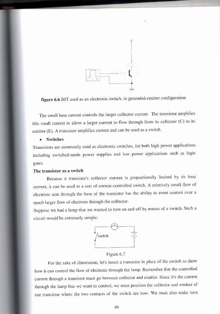
•
figure 6.6 BJT used as an electronic switch, in grounded-emitter configuration
The small base current controls the larger collector current. The transistor amplifies
this small current to allow a larger current to flow through from its collector (C) to its
emitter (E). A transistor amplifies current and can be used as a switch.
• Switches Transistors are commonly used as electronic switches, for both high power applications
including switched-mode power supplies and low power applications such as logic
gates.
The transistor as a switch Because a transistor's collector current is proportionally limited by its base
current, it can be used as a sort of current-controlled switch. A relatively small flow of
electrons sent through the base of the transistor has the ability to exert control over a
much larger flow of electrons through the collector.
Suppose we had a lamp that we wanted to tum on and off by means of a switch. Such a
circuit would be extremely simple:
Figure 6.7
For the sake of illustration, let's insert a transistor in place of the switch to show
how it can control the flow of electrons through the lamp. Remember that the controlled
current through a transistor must go between collector and emitter. Since it's the current
through the lamp that we want to control, we must position the collector and emitter of
our transistor where the two contacts of the switch are now. We must also make sure
49

•
that the lamp's current will move against the direction of the emitter arrow symbol to
ensure that the transistor's junction bias will be correct:
NPN transistor
Figure 6.8
In this example was choosen an NPN transistor. A PNP transistor could also
have been chosen for the job, and its application would look like this:
PNP transistor
Figure 6.9
The choice between NPN and PNP is really arbitrary. All that matters is that the
proper current directions are maintained for the sake of correct junction biasing
(electron flow going against the transistor symbol's arrow).
Going back to the NPN transistor in our example circuit, we are faced with the need to
add something more so that we can have base current. Without a connection to the base
wire of the transistor, base current will be zero, and the transistor cannot tum on,
resulting in a lamp that is always off. Remember that for an NPN transistor, base current
must consist of electrons flowing from emitter to base (against the emitter arrow
symbol, just like the lamp current). Perhaps the simplest thing to do would be to connect
a switch between the base and collector wires of the transistor like this:
switch
figure 6.10
If the switch is open, the base wire of the transistor will be left "floating" (not
connected to anything) and there will be no current through it. In this state, the transistor
is said to be cutoff. If the switch is closed, however, electrons will be able to flow from
the emitter through to the base of the transistor, through the switch and up to the left
50

,/.r .•.
• l . // '<i' •\
/! :..-; ') side of the lamp, back to the positive side of the battery. This base curreUtc~till enablea ·_. '
\\ ,, \ \ \ ~' ~-<··.. ••• ~- much larger flow of electrons from the emitter through to the collector, t~§'° lighting up {:,I').,, J
the lamp. In this state of maximum circuit current, the transistor is said to b~~~~·f
switch
Figure 6.11
Of course, it may seem pointless to use a transistor in this capacity to control the
lamp. After all, we're still using a switch in the circuit, aren't we? If we're still using a
switch to control the lamp -- if only indirectly -- then what's the point of having a
transistor to control the current? Why not just go back to our original circuit and use the
switch directly to control the lamp current?
There are a couple of points to be made here, actually. First is the fact that when
used in this manner, the switch contacts need only handle what little base current is
necessary to tum the transistor on, while the transistor itself handles the majority of the
lamp's current. This may be an important advantage if the switch has a low current
rating: a small switch may be used to control a relatively high-current load. Perhaps
more importantly, though, is the fact that the current-controlling behavior of the
transistor enables us to use something completely different to tum the lamp on or off.
• Amplifiers From mobile phones to televisions, vast numbers of products include amplifiers
for sound reproduction, radio transmission, and signal processing. The first discrete
transistor audio amplifiers barely supplied a few hundred milliwatts, but power and
audio fidelity gradually increased as better transistors became available and amplifier
architecture evolved.
Transistors are commonly used in modem musical instrument amplifiers, where
circuits up to a few hundred watts are common and relatively cheap. Transistors have
largely replaced valves in instrument amplifiers. Some musical instrument amplifier
manufacturers mix transistors and vacuum tubes in the same circuit, to utilize the
inherent benefits of both devices.
51

..
• Computers
The "first generation" of electronic computers used vacuum tubes, which
generated large amounts of heat, were bulky, and were unreliable. The development of
the transistor was key to computer miniaturization and reliability. The "second
generation" of computers, through the late 1950s and 1960s featured boards filled with
individual transistors and magnetic memory cores. Subsequently, transistors, other
components, and their necessary wiring were integrated into a single, mass
manufactured component: the integrated circuit. Transistors incorporated into integrated
circuits have replaced most discrete transistors in modem digital computers.
• Using a transistor switch with sensors +Vs
.___ ov
Figure 6.12 LED lights when the LDR is dark
+Vs
470
.__ _. __ (f\/
Figure 6.13 LED lights when the LDR is bright
The top circuit diagram shows an LDR (light sensor) connected so that the LED
lights when the LDR is in darkness. The variable resistor adjusts the brightness at which
the transistor switches on and off. Any general purpose low power transistor can be
used in this circuit.
The 1 OkJ:2 fixed resistor protects the transistor from excessive base current
(which will destroy it) when the variable resistor is reduced to zero. To make this circuit
52
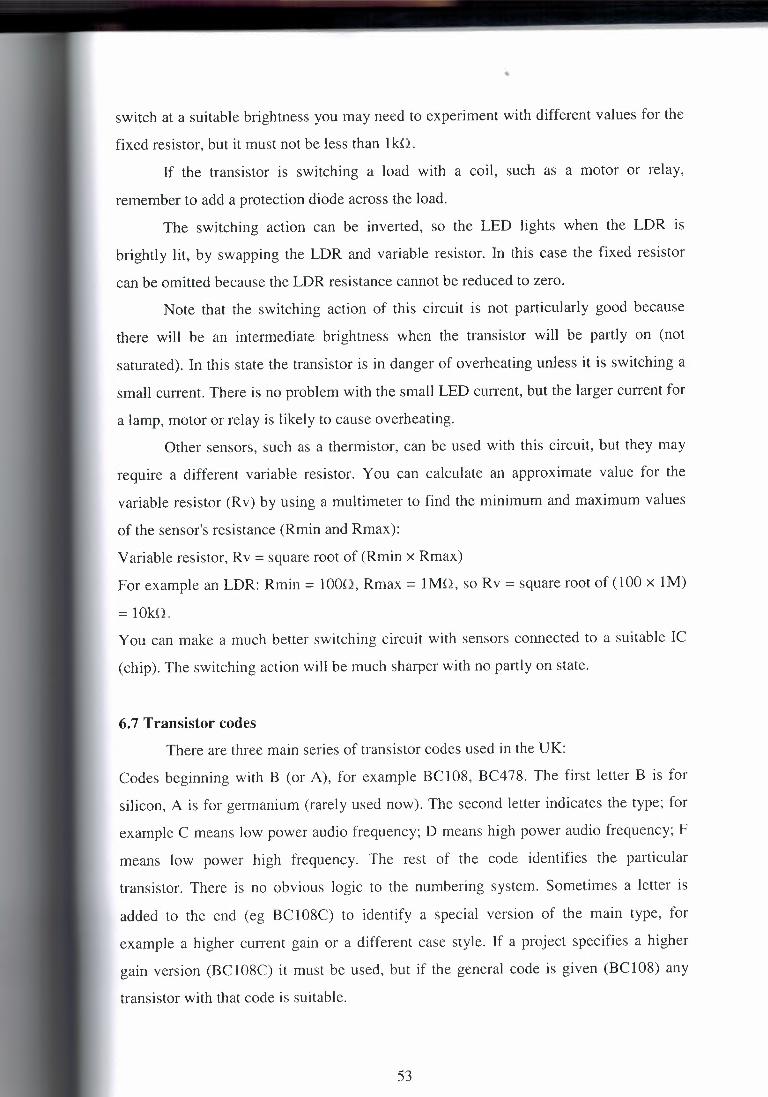
•
switch at a suitable brightness you may need to experiment with different values for the
fixed resistor, but it must not be less than I kn.
If the transistor is switching a load with a coil, such as a motor or relay,
remember to add a protection diode across the load.
The switching action can be inverted, so the LED lights when the LDR is
brightly lit, by swapping the LDR and variable resistor. In this case the fixed resistor
can be omitted because the LDR resistance cannot be reduced to zero.
Note that the switching action of this circuit is not particularly good because
there will be an intermediate brightness when the transistor will be partly on (not
saturated). In this state the transistor is in danger of overheating unless it is switching a
small current. There is no problem with the small LED current, but the larger current for
a lamp, motor or relay is likely to cause overheating.
Other sensors, such as a thermistor, can be used with this circuit, but they may
require a different variable resistor. You can calculate an approximate value for the
variable resistor (Rv) by using a multimeter to find the minimum and maximum values
of the sensor's resistance (Rmin and Rmax):
Variable resistor, Rv = square root of (Rmin x Rmax)
For example an LDR: Rmin = lOOn, Rmax = IMO, so Rv = square root of (100 x IM)
= l Oktr. You can make a much better switching circuit with sensors connected to a suitable IC
(chip). The switching action will be much sharper with no partly on state.
6.7 Transistor codes There are three main series of transistor codes used in the UK:
Codes beginning with B (or A), for example BC108, BC478. The first letter B is for
silicon, A is for germanium (rarely used now). The second letter indicates the type; for
example C means low power audio frequency; D means high power audio frequency; F
means low power high frequency. The rest of the code identifies the particular
transistor. There is no obvious logic to the numbering system. Sometimes a letter is
added to the end ( eg BC I 08C) to identify a special version of the main type, for
example a higher current gain or a different case style. If a project specifies a higher
gain version (BC108C) it must be used, but if the general code is given (BC108) any
transistor with that code is suitable.
53

•
• Codes beginning with TIP, for example TIP31A TIP refers to the manufacturer: Texas Instruments Power transistor. The letter at the
end identifies versions with different voltage ratings.
• Codes beginning with 2N, for example 2N3053 The initial '2N' identifies the part as a transistor and the rest of the code
identifies the particular transistor. There is no obvious logic to the numbering
system.
6.8 Choosing a transistor Most projects will specify a particular transistor, but if necessary you can usually
substitute an equivalent transistor from the wide range available. The most important
properties to look for are the maximum collector current IC and the current gain hFE.
To make selection easier most suppliers group their transistors in categories determined
either by their typical use or maximum power rating.
To make a final choice you will need to consult the tables of technical data
which are normally provided in catalogues. They contain a great deal of useful
information but they can be difficult to understand if you are not familiar with the
abbreviations used.
54

•
CHAPTER 7. DARLINGTON PAIR OF TRANSISTORS
7.1 Overview In electronics, the Darlington transistor is a semiconductor device which
combines two bipolar transistors in tandem ( often called a "Darlington pair") in a single
device so that the current amplified by the first is amplified further by the second
transistor. This gives it high current gain (written ~ or hFE), and takes up less space
than using two discrete transistors in the same configuration. The use of two separate
transistors in an actual circuit is still very common, even though integrated packaged
devices are available.
Transistors are an essential component in a sensor circuit. Usually transistors are
arranged as a pair, known as a 'darlington pair'. It is very important that we can identify
this arrangement of transistors and state clearly why they are used.
A darlington pair is used to amplify weak signals so that they can be clearly detected by
another circuit or a computer/microprocessor.
A Darlington pair behaves like a single transistor with a very high current gain.
This is beneficial as many commonly-used transistors with high gains have a low
current threshold. The total gain of the Darlington is the product of the gains of the
individual transistors: ~Darlington = ~ 1 x~2 . The base-emitter voltage is also higher; it
is the sum of both base-emitter voltages: VBE = VB El + VBE2 To tum on there must be -0.6 V across both base-emitter junctions which are
connected in series inside the Darlington pair. It therefore requires more than 1.2 V to
tum on. When a Darlington pair is fully conducting, there is a residual saturation
voltage of 0.6 V in this configuration, which can lead to substantial power dissipation.
Another drawback is that the switching speed can be slow, due to the inability of the
first transistor to actively inhibit the current into the base of the second device. This can
make the pair slow to switch off. To alleviate this, a resistor of a few hundred ohms
between the second device's base and emitter is often used. Integrated Darlington pairs
often include this resistor.
The circuit below is a 'Darlington Pair' driver. The first transistor's emitter feeds
into the second transistor's base and as a result the input signal is amplified by the time
it reaches the output. The important point to remember is that the Darlington Pair is
55

•
made up of two transistors and when they are arranged as shown in the circuit they are
used to amplify weak signals.
figure 7.1 Darlington pair driver
The circuit to the below shows a single transistor. When the switch is pressed
current flows from the 9v to the Ov and also to the base of the transistor. This allows the
transistor to switch and in tum, current I voltage flows through the bulb, which lights.
However, there is a potential problem with this circuit. The signal I current at the base
of the transistor may be too weak to switch the transistor and allow the bulb to light or it
may flicker on and off.
figure 7 .2 single transistor circuit
A possible solution is seen below. A second transistor is added to the circuit, the
circuit is now likely to work as the original signal I current is amplified.
The amount by which the weak signal is amplified is called the 'GAIN'.
figure 7 .3 darlington pair two transistors
56

This is two transistors connected together so that the current amplified by the
first is amplified further by the second transistor. The overall current gain is equal to the
two individual gains multiplied together:
Darlington pair current gain, hFE = hFEl x hFE2 (hFEl and hFE2 are the gains of the
individual transistors). This gives the Darlington pair a very high current gain, such as
10000, so that only a tiny base current is required to make the pair switch on.
A Darlington pair behaves like a single transistor with a very high current gain.
It has three leads (B, C and E) which are equivalent to the leads of a standard individual
transistor. To tum on there must be 0.7V across both the base-emitter junctions which
are connected in series inside the Darlington pair, therefore it requires 1.4 V to tum on.
Darlington pairs are available as complete packages but you can make up your own
from two transistors; TRl can be a low power type, but normally TR2 will need to be
high power. The maximum collector current Ic(max) for the pair is the same as Ic(max)
for TR2.
figure 7.4 darlington pair of two transistors
This is two transistors connected together so that the amplified current from the first is
amplified further by the second transistor. This gives the Darlington pair a very high
current gain such as 10000. Darlington pairs are sold as complete packages containing
the two transistors. They have three leads (B, C and E) which are equivalent to the leads
of a standard individual transistor.
You can make up your own Darlington pair from two transistors.
For example:
For TRl use BC548B with hFEl = 220. For TR2 use BC639 with hFE2 = 40. The overall gain of this pair is hFEl x hFE2 = 220 x 40 = 8800. The pair's maximum collector current IC(max) is the same as TR2.
57
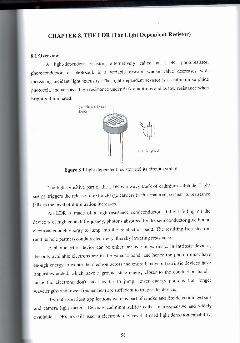
CHAPTER 8. THE LDR (The Light Dependent Resistor)
8.1 Overview A light-dependent resistor, alternatively called an LDR, photoresistor,
photoconductor, or photocell, is a variable resistor whose value decreases with
increasing incident light intensity. The light dependent resistor is a cadmium-sulphide
photocell, and acts as a high resistance under dark cmditions and as low resistance when
brightly illuminated.
cadmium sulphide track
circuit symbol
figure 8.1 light dependent resistor and its circuit symbol
The light-sensitive part of the LDR is a wavy track of cadmium sulphide. Light
energy triggers the release of extra charge carriers in this material, so that its resistance
falls as the level of illumination increases.
An LDR is made of a high-resistance semiconductor. If light falling on the
device is of high enough frequency, photons absorbed by the semiconductor give bound
electrons enough energy to jump into the conduction band. The resulting free electron
(and its hole partner) conduct electricity, thereby lowering resistance.
A photoelectric device can be either intrinsic or extrinsic. In intrinsic devices,
the only available electrons are in the valence band, and hence the photon must have
enough energy to excite the electron across the entire bandgap. Extrinsic devices have
impurities added, which have a ground state energy closer to the conduction band -
since the electrons don't have as far to jump, lower energy photons (i.e. longer
wavelengths and lower frequencies) are sufficient to trigger the device.
Two of its earliest applications were as part of smoke and fire detection systems
and camera light meters. Because cadmium sulfide cells are inexpensive and widely
available, LDRs are still used in electronic devices that need light detection capability,
58

such as security alarms, street lamps, and clock radios. Other apllications are in camera,
strobe ( colour temperature reading) clocks, switch for lighting and optical switches.
8.2 Applications of LDR The LDR or light Dependent Resistor are very useful especially in light/dark
sensor circuits. Normally the resistance of an LDR is very high, sometimes as high as 1
MO., but when they are illuminated with light, resistance drops.
Figure 8.2 a LDR
When the light level is low the resistance of the LDR is high. This prevents current from
flowing to the base of the transistors. Consequently the LED does not light. However,
when light shines onto the LDR its resistance falls and current flows into the base of the
first transistor and then the second transistor. The LED lights.
8.2.1 Light Sensors A light sensor is a sensor that measures the amount of light that it sees. It reports
the amount of light to the RCX as a number between O (total darkness) and 100 (very
bright).
The light sensor detects light from a very wide angle. You can narrow its
detection field by placing a lx2 beam with a hole in front of the sensor. Now the light
sensor will only detect light that is directly in front of it.
LED
Figure 8.3 this is an example of a light sensor circuit. The preset resistor can be turned
up or down to increase or decrease resistance, in this way it can make the circuit more
or less sensitive.
59

Light sensors are devices that senses the light pulses in an optical fiber and
converts them into electrical pulses. It uses the principle of photoconductivity, which is
exhibited in certain materials that change their electrical conductivity when exposed to
light.
Everything has an electrical resistance, some more than others. An LDR will
have a resistance that varies according to the amount of visible light that falls on it. A
close up of an LDR is shown below:
figure 8.4 ldr
The light falling on the brown zigzag lines on the sensor, causes the resistance of the
device to fall. This is known as a negative co-efficient. There are some LDRs that
work in the opposite way i.e. their resistance increases with light.
• Photocells Photocells act as light sensors. Photocell is a solid-state device that converts
light into electrical energy by producing a voltage, as in a photovoltaic cell, or uses light
to regulate the flow of current, as in a photoconductive cell. It is used in automatic
control systems for doors, lighting, etc. Photocells measure light levels, allowing
artificial lighting to supplement natural daylight. Inlike infrared sensors that are good
for line followers or detecting the presense of an object, photocells are good when you
just want to detect light. For example, you might want a sensor that detects when a
flashlight is on, or when the sun is out. Photocells are used in automatic night lights and
in street lamps that tum themselves on at night.
figure 8.5 photocell
60
• Available in center tap dual cell configurations as well as specially selected resistance
ranges for special applications • Easy to use in DC or AC circuits - they are a light variable resistor and hence
symmetrical with respect to AC waveforms • Usable with almost any visible or near infrared light source such as LEDS; neon;
fluorescent, incandescent bulbs, lasers; flame sources;
sunlight; etc • Available in a wide range of resistance values
Applications Photoconductive cells are used in many different types of circuits and
applications. Suitable for low voltage battery operation of many demanding applications such
as, security lights, street lights, CCTVs, backlight controls for LCDs, PDAs, mobile
phones, car navigation systems etc. dimmers for keypads, clocks and watches , Cam
eras , automotive, rain, light and tunnel systems.
Analog Applications
• Camera Exposure Control
• Auto Slide Focus - dual cell • Photocopy Machines - density of toner
• Colorimetric Test Equipment
• Densitometer • Electronic Scales - dual cell • Automatic Gain Control - modulated light source
• Automated Rear View Mirror
Digital Applications
• Automatic Headlight Dimmer
• Night Light Control
• Oil Burner Flame Out
• Street Light Control
• Position Sensor
62

Photocells With Lead Free Terminals This small 'coated' CdS cell has lead free terminals that will withstand a
soldering temperature of up to 260°C for 3 seconds at a distance of 5mm from its base.
This cell is suitable for applications granted freedom to use CdS cells by an exclusion
from RoHS.
Applications: • Automatic Lighting
• Camera exposure control • Automatic photoelectric control
• Opto-electronic coupling • Automatic photoelectric inspection
• Photoelectric light-controlled toys
8.1.2 PHOTORESISTOR A photoresistor is an electronic component whose resistance decreases with
increasing incident light intensity. It can also be referred to as a light-dependent resistor
(LDR), photoconductor, or photocell. A photoresistor is made of a high-resistance semiconductor. If light falling on
the device is of high enough frequency, photons absorbed by the semiconductor give
bound electrons enough energy to jump into the conduction band. The resulting free
electron ( and its hole partner) conduct electricity, thereby lowering resistance.
Figure 8.7 The internal components of a photoelectric control for a typical streetlight.
The photoresistor is facing rightwards, and controls whether current flows
through the heater which opens the main power contacts. At night, the heater cools,
closing the power contacts, energizing the street light. The heater/bimetal mechanism
provides a built-in time-delay.
• A photoelectric device can be either intrinsic or extrinsic. An intrinsic
semiconductor has its own charge carriers and is not an efficient semiconductor, eg.
silicon. ln intrinsic devices, the only available electrons are in the valence band, and
hence the photon must have enough energy to excite the electron across the entire
bandgap. Extrinsic devices have impurities added, which have a ground state energy
closer to the conduction band - since the electrons don't have as far to jump, lower
energy photons (i.e. longer wavelengths and lower frequencies) are sufficient to trigger
the device. If a sample of silicon has some of its atoms replaced by phosphorus
atoms(impurities), there will be extra electrons available for conduction. This is an
example of an extrinsic semiconductor. Cadmium sulphide or cadmium sulphide (CdS) cells rely on the material's ability
to vary its resistance according to the amount of light striking the cell. The more light
that strikes the cell, the lower the resistance. Although not accurate, even a simple CdS
cell can have a wide range of resistance from less than 100 D in bright light to in excess
of 10 MD in darkness. Many commercially available CdS cells have a peak sensitivity
in the region of 500nm - 600nm. The cells are also capable of reacting to a broad range
of frequencies, including infrared (IR), visible light, and ultraviolet (UV). They are
often found on street lights as automatic on/off switches. They were once even used in
heat-seeking missiles to sense for targets.
Applications Photoresistors come in many different types. Inexpensive cadmium sulphide
cells can be found in many consumer items such as camera light meters, clock radios,
security alarms, street lights and outdoor clocks. They are also used in some dynamic
compressors to control gain reduction. At the other end of the scale, Ge.Cu
photoconductors are among the best far-infrared detectors available, and are used for
infrared astronomy and infrared spectroscopy.
64

CHAPTER 9. BUZZER
9.1 Overview Buzzer is a transducer which converts electrical energy to sound. A transducer is
a device, usually electrical, electronic, or electro-mechanical, that converts one type of
energy to another for various purposes including measurement or information transfer.
In a broader sense, a transducer is sometimes defined as any device that converts a
signal from one form to another. For example, an LDR is an input transducer (sensor) which converts brightness
(light) to resistance. It is made from cadmium sulphide (CdS) and the resistance
decreases as the brightness of light falling on the LDR increases.
Transducers are electric or electronic devices that transform energy from one
manifestation into another. Anything that converts energy can be considered a
transducer. Transducers that detect or transmit information include common items such
as microphones, Geiger meters, potentiometers, pressure sensors, thermometers, and
antennae. A microphone, for example, converts sound waves that strike its diaphragm
into an analogous electrical signal that can be transmitted over wires. A pressure sensor
turns the physical force being exerted on the sensing apparatus into an analog reading
that can be easily represented Most transducers have an inverse that allows for the energy to be returned to its
original form. Audio cassettes, for example, are created by using a transducer to tum the
electrical signal from the microphone pick-up - which in tum went through a transducer
to convert the sound waves into electrical signal - into magnetic fluctuations on the tape
head. These magnetic fluctuations are then read and converted by another transducer -
in this case a stereo system - to be turned back into an electrical signal, which is then
fed by wire to speakers, which act as yet another transducer to tum the electrical signal
back into audio waves. Other transducers tum one type of energy into another form, not for the purpose
of measuring something in the external environment or to communicate information,
but rather to make use of that energy in a more productive manner. A light bulb, for
example, one of the many transducers around us in our day-to-day lives, converts
electrical energy into visible light. Electric motors are another common form of
electromechanical transducer, converting electrical energy into kinetic energy to
perform a mechanical task. The inverse of an electric motor - a generator - is also a
65

•
transducer, turning kinetic energy into electrical energy that can then be used by other
devices. As in all energy conversions, some energy is lost when transducers operate. The
efficiency of a transducer is found by comparing the total energy put into it to the total
energy coming out of the system. Some transducers are very efficient, while others are
extraordinarily inefficient. A radio antenna, for example, acts as a transducer to tum
radio frequency power into an electromagnetic field; when operating well, this process
is upwards of 80% efficient. Most electrical motors, by contrast, are well under 50%
efficient, and a common light bulb, because of the amount of energy lost as heat, is less
than 10% efficient.
An electronic buzzer comprises an acoustic vibrator comprised of a circular
metal plate having its entire periphery rigidly secured to a support, and a piezoelectric
element adhered to one face of the metal plate. A driving circuit applies electric driving
signals to the vibrator to vibrationally drive it at a 1/N multiple of its natural frequency,
where N is an integer, so that the vibrator emits an audible buzzing sound. The metal
plate is preferably mounted to undergo vibration in a natural vibration mode having
only one nodal circle. The drive circuit includes an inductor connected in a closed loop
with the vibrator, which functions as a capacitor, and the circuit applies signals at a
selectively variable frequency to the closed loop to accordingly vary the inductance of
the inductor to thereby vary the period of oscillation of the acoustic vibrator and the
resultant frequency of the buzzing sound.
Buzzer is an electric signaling device, such as a doorbell, that makes a buzzing
sound. A buzzer or beeper is a signalling device, usually electronic, typically used in
automobiles, household appliances such as a microwave oven, or game shows.
It most commonly consists of a number of switches or sensors connected to a
control unit that determines if and which button was pushed or a preset time has lapsed,
and usually illuminates a light on the appropriate button or control panel, and sounds a
warning in the form of a continuous or intermittent buzzing or beeping sound. Initially
this device was based on an electromechanical system which was identical to an electric
bell without the metal gong (which makes the ringing noise). Often these units were
anchored to a wall or ceiling and used the ceiling or wall as a sounding board. Another
implementation with some AC-connected devices was to implement a circuit to make
the AC current into a noise loud enough to drive a loudspeaker and hook this circuit up
to a cheap 8-ohm speaker. Nowadays, it is more popular to use a ceramic-based
66

piezoelectric sounder like a Sonalert which makes a high-pitched tone. Usually these
were hooked up to "driver" circuits which varied the pitch of the sound or pulsed the
sound on and off. The word "buzzer" comes from the rasping noise that buzzers made when they
were electromechanical devices, operated from stepped-down AC line voltage at 50 or
60 cycles. Other sounds commonly used to indicate that a button has been pressed are a
ring or a beep. Some systems, such as the one used on Jeopardy!, make no noise at all,
instead using light.
Figure 9.1 electric buzzers
Buzzer and Bleeper These devices are output transducers converting electrical energy to sound. They
contain an internal oscillator to produce the sound which is set at about 400Hz for
buzzers and about 3kHz for bleepers. Buzzers have a voltage rating but it is only approximate, for example 6V and
12V buzzers can be used with a 9V supply. Their typical current is about 25mA.
Bleepers have wide voltage ranges, such as 3-30V, and they pass a low current of about
1 OmA. Buzzers and bleepers must be connected the right way round, their red lead is
positive ( + ).
,{{I;) '
Q " " ~
Figure 9.2 buzzers
6
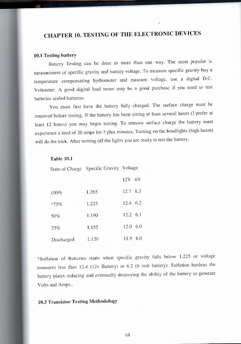
CHAPTER 10. TESTING OF THE ELECTRONIC DEVICES
10.1 Testing battery Battery Testing can be done in more than one way. The most popular is
measurement of specific gravity and battery voltage. To measure specific gravity buy a
temperature compensating hydrometer and measure voltage, use a digital D.C.
Voltmeter. A good digital load tester may be a good purchase if you need to test
batteries sealed batteries. You must first have the battery fully charged. The surface charge must be
removed before testing. If the battery has been sitting at least several hours (I prefer at
least 12 hours) you may begin testing. To remove surface charge the battery must
experience a load of 20 amps for 3 plus minutes. Turning on the headlights (high beam)
will do the trick. After turning off the lights you are ready to test the battery.
Table 10.1
State of Charge Specific Gravity Voltage
12V 6V
100% 1.265 12.7 6.3
*75% 1.225 12.4 6.2
50% 1.190 12.2 6.1
25% 1.155 12.0 6.0
Discharged 1.120 11.9 6.0
*Sulfation of Batteries starts when specific gravity falls below 1.225 or voltage
measures less than 12.4 (12v Battery) or 6.2 (6 volt battery). Sulfation hardens the
battery plates reducing and eventually destroying the ability of the battery to generate
Volts and Amps ..
10.2 Transistor Testing Methodology
68

·.
You can think of a transistor as two back-to-back diodes in one package as shown in
figure.
C C
PNP Figure 5
E E
Transistors come in many different case styles, three of which are shown in
Figure 10.1. It is important to know where C, B, E are for any given case. Assuming it
is known that if the transistor is NPN or PNP, and assuming it is known where B, C, and
E are, then just test the B-C junction and the B-E junction as if they were standard
diodes. if one of those junctions is a "bad diode", then the transistor is bad.
0\ Metal Case iVisC <D DB) ,;
E C B C E ~ B
Figure 10.1 different case styles of transistors
The best way to test transistors with a DMM is to make use of the "diode test"
function. For this method, if we read a short circuit (0 Ohms or voltage drop of 0), or
the transistor fails any of the readings, it is bad and must be replaced. Connect the meter
leads with the polarity as shown and verify that the base-to-emitter and base-tocollector
junctions read as a forward biased diode: 0.5 to 0.8 VDC. Reverse the meter
connections to the transistor and verify that both PN junctions do not conduct. Meter
should indicate an open circuit. (Display= OUCH or OL.)
Finally read the resistance from emitter to collector and verify an open circuit
reading in both directions. (Note: A short can exist from emitter to collector even if the
individual PN junctions test properly.) Assuming it is known that if the transistor is
NPN or PNP, and assuming it is known where B, C, and E are, then B-C junction and
69

the B-E junction can be tested as if they were standard diodes. If one of those junctions
is a "bad diode", then the transistor is bad.
Also, check the resistance from C to E using a higher Ohms scale (say, the 2
Meg scale). Be sure your fingers don't touch the metal test points or you will just
measure your skin resistance.
If the transistor is good, you should get an open-circuit reading from collector to
emitter.A transistor can be tested for shorts, opens, or leakage, as though it is just a pair
of connected diodes.
Usmg Meter To Separate Npn From Pnp If it does not known if the transistor is NPN or PNP, then it can be found out
which it is using Ohm-meter if it is known which lead of your meter is positive.
Assuming it's known where C, B, and E are on the transistor, the following must be
done: Connect the positive lead of the Ohm-meter to the base. Touch the other lead of your
meter to the collector. If there is a reading, the transistor is NPN. To verify, move the
lead from the collector to the emitter and you should still get a reading.
If the meter reads open-circuit, then connect the negative lead to the base and touch the
positive lead to the collector. If there is a reading, then the transistor is PNP. Verify by
measuring from base to emitter.
Testing with a (Digital) DMM Set your meter to the diode test. Connect the red meter lead to the base of the
transistor. Connect the black meter lead to the emitter. A good NPN transistor will read
a junction drop voltage of between .45v and .9v. A good PNP transistor will read
OPEN. Leave the red meter lead on the base and move the black lead to the collector.
The reading should be the same as the previous test. Reverse the meter leads in your
hands and repeat the test. This time, connect the black meter lead to the base of the
transistor. Connect the red meter lead to the emitter. A good PNP transistor will read a
JUNCTION DROP voltage of between .45v and .9v. A good NPN transistor will read
OPEN. Leave the black meter lead on the base and move the red lead to the collector.
The reading should be the same as the previous test. Place one meter lead on the
collector, the other on the emitter. The meter should read OPEN. Reverse your meter
70

leads. The meter should read OPEN. This is the same for both NPN and PNP
transistors.
10.3 Testing Darlington Transistors A Darlington is a special type of configuration usually consisting of 2 transistors
fabricated on the same chip or at least mounted in the same package. Discrete
implementations as well as Darlingtons with more than 2 transistors are also possible.
In many ways, a Darlington configuration behaves like a single transistor where:
the current gains (Hfe) of the individual transistors it is composed of are multiplied
together and, the B-E voltage drops of the individual transistors it is composed of are
added together. Darlingtons are used where drive is limited and the high gain - typically
over 1,000 - is needed. Frequency response is not usually that great, however.
Testing with a VOM or DMM is basically similar to that of normal bipolar
transistors except that in the forward direction, B-E will measure higher than a normal
transistor on a VOM (but not open and 1.2 to 1.4 V on a DMM's diode test range due to
the pair of junctions in series. Note, 1.2 V may be too high for some DMMs and thus a
good Darlington may test open - confirm that the open circuit reading on your DMM is
higher than 1.4 V or check with a known good Darlington.
10.4 Testing LEDs Electrically, LEDs behave like ordinary diodes except that their forward voltage
drop is higher.
Typical values are:
An LED can be weak and still pass the electrical tests so checking for output is still
necessary.
Color Potential Difference
Infrared 1.6 V
Red 1.8Vto2.1 V
Orange 2.2 V
Yellow 2.4 V
Green 2.6 V
Blue 3.0 V to 3.5 V
71
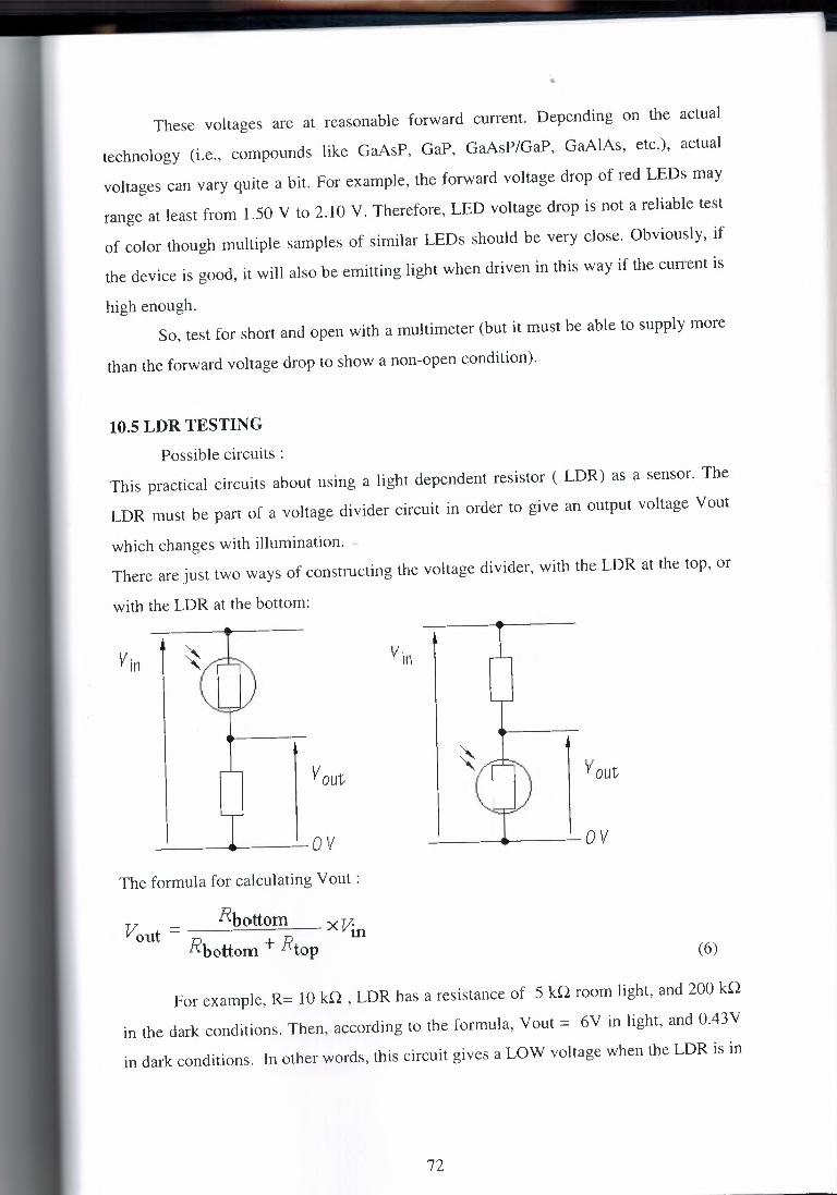
·. These voltages are at reasonable forward current Depending on the actual
technology (i.e., compounds like GaAsP, GaP, GaAsP/GaP, GaAlAs, etc.), actual
voltages can vary quite a bit For example, the forward voltage drop of red LEDs may
range at least from 1.50 V to 2. 10 V. Therefore, LED voltage drop is not a reliable test
of color though multiple samples of similar LEDs should be very close. Obviously, if
the device is good, it will also be emitting light when driven in this way if the current is
high enough. So, test for short and open with a multimeter (but it must be able to supply more
than the forward voltage drop to show a non-open condition).
10.5 LDR TESTING Possible circuits :
This practical circuits about using a light dependent resistor ( LDR) as a sensor. The
LDR must be part of a voltage divider circuit in order to give an output voltage Vout
which changes with illumination. There are just two ways of constructing the voltage divider, with the LDR at the top, or
with the LDR at the bottom:
~1 in
v' out
__ __._ Q\/
The formula for calculating Vout :
Rbottorn xvin Rbottom + Rtop (6)
For example, R= 10 kQ , LDR has a resistance of 5 kQ room light, and 200 kQ
in the dark conditions. Then, according to the formula, Vout = 6V in light, and 0.43V
in dark conditions. In other words, this circuit gives a LOW voltage when the LDR is in
72
the shade, and a HIGH voltage when the LDR is in the light. The voltage divider circuit
gives an output voltage which changes with illumination.
We can measure the LDR'S resistance by using multimeter as an ohmmeter to see if our
LDR is ok or not. First we measure it under light conditions, then in the dark conditions
and compare the results. It doesn't need to shine light directly onto the LDR. If the reading on the meter
changes as shadows fall onto the surface of the LDR, LDR is ok. Now cover the LDR
with your hand so that it is in the shade. The resistance of the LDR will increase.
The voltage divider is most sensitive when the resistance of the fixed resistor is
equal to the resistance of the LDR. Voltage dividers are most sensitive when Rbottom
and Rtop have equal values Perhaps first circuit should be called a dark sensor, since it gives a HIGH Vout
when the LDR is covered. The action of the voltage divider is reversed when the LDR is used as Rbottom
instead of as Rtop.
Conclusions It matters what value of fixed resistor used in a voltage divider.
The optimum value of fixed resistor gives the biggest changes in Vout . This happens
when Rbottom = Rtop. It can be decided that how a voltage divider circuit is going to work by thinking about
whether to use the sensor component as Rbonom or as Rtop .
73
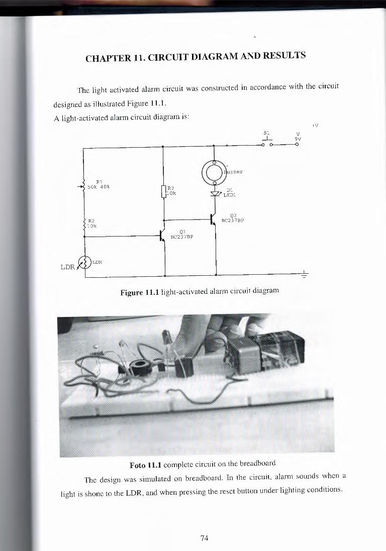
CHAPTER 11. CIRCUIT DIAGRAM AND RESULTS
The light activated alarm circuit was constructed in accordance with the circuit
designed as illustrated Figure 11.1.
A light-activated alarm circuit diagram is: +V
Sl V _L 9V 0 0
Rl 50k 40% R3
10k
LDR
Q2 BC237BP
Ql BC237BP
Figure 11.1 light-activated alarm circuit diagram
Foto 11.1 complete circuit on the breadboard
The design was simulated on breadboard. In the circuit, alarm sounds when a
light is shone to the LDR, and when pressing the reset button under lighting conditions.
74
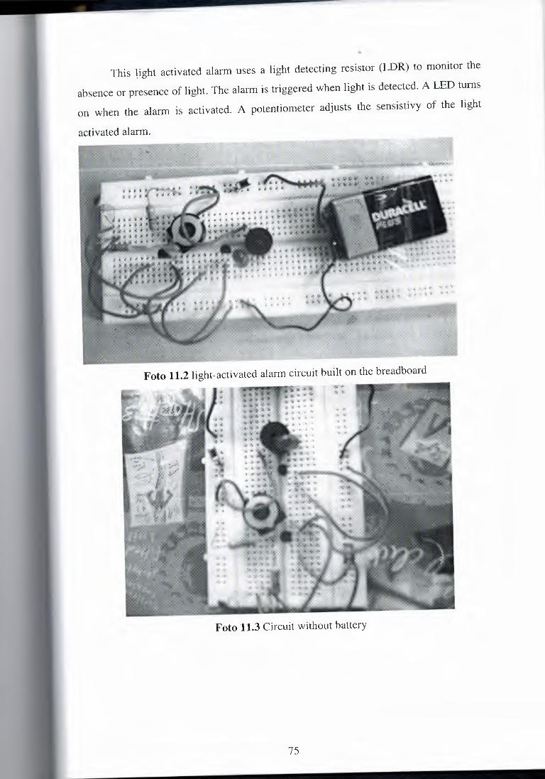
• This light activated alarm uses a light detecting resistor (LDR) to monitor the
absence or presence of light. The alarm is triggered when light is detected. A LED turns
on when the alarm is activated. A potentiometer adjusts the sensistivy of the light
activated alarm.
Foto 11.2 light-activated alarm circuit built on the breadboard
Foto 11.3 Circuit without battery
75

•
Foto 11.4 light activated alarm circuit simulated on the breadboard
The LDR in this circuit, is set up with a transistor in such a way so that in light
condition, it's resistance is low, allowing current to trigger the transistor Ql. When the
light is low, the resistance of the LDR is too much and the transistor is not triggered.
The amount of light needed (sensitivity) to switch the transistor can be adjusted by Rl,
which sets the bypass level of the transistor. Once the Ql is triggered, it acts with Q2 as
a Darlington pair. The warning sound is transmitted throughout the speaker and the as
LED is lighted.
The LDR and 1 Ok resistor and 50k potentiometer form a potential divider that
supplies the transistor 1. When the LDR is in the dark, its resistance is high, there is a
large voltage across the LDR. There is a voltage drop across the base of the transistor so
that the base is at 0.7V. The resistor R3 limits the current to the base. The transistor is
turned on. It can allow a big enough current to flow to turn the alarm on.
Transistors with darlington pair is used for higher current gain for turn on the
buzzer. After darlington paired transistors are triggered, alarm is turned on and activated
and it sounds and at the same time LED emits light for viewable warning.
Under dark conditions, the LDR presents a high resistance, so transistors are not
triggered and so alarm doesn't sound.
Whne the LDR is illuminated, its resistance falls to a low value, and transistors
are triggered and so alarm is turned on and it sounds.
76

The sensitivity of this alarm circuit can be adjusted by adjusting the 50k
potentiometer. When the potentiometer resistance is increased, from the voltage divider,
voltage on the LDR is decreasing, and so less light can activate the circuit.
11.1 Results of testing the circuit elements
Transistor BC237 testing results:
Under diode test: VBC = 1572 mV and VBE = 1570 mV. These values are normal on forward biased
junction, and when the polarities reversed there is no conduction. So this transistors
passed this test.
Transistor resistances are: RBC = 5.2 MO, RBE = 5 MO, and REC = open circuit, so this transistors passed this
test too. Under operation, BC237 voltgaes are: VCE =0.73V VEB = 1.2V under light
conditions.
Under shade, VCE = 0.09 and VEB = 1.5V.
Transistor H237 test results:
VBC = 655.5 mV and VBE = 654mV. These are normal values for this transistor.
Resistances are: RBC = 5.77 MO, RBE = 5.8 MO, REC = open circuit. So it passed
the test. Under operation, under light conditions: VCE = 2.78V , VEB =0.7V
Under shade conditions: VCE = 1 OV and VEB =OV.
Buzzer: When the buzzer resistance is measured, it is seen that it is 0.53 MO. The
resistance of the buzzer is a little big, so voltage drop on the buzzer is is high.
On the diode test function on the multimeter, voltage drop of the buzzer is 1745m V.
During the operation of the circuit under the light conditions, the voltage on the buzzer
is 7V. Under dark conditions, that voltage is 0.23 volt, so buzzer does not operate, so it
does not give sound.
77

LDR test results:
Under daylight conditions, LDR resistance is measured 6.5 kO, when it is shaded its
resistance becomes changing between 40 - 50 kO, and under dark conditions whne it is
closed by a box, its resistance becomes nearly 20 MO.
LED test result:
When the LED used in the circuit connected to multimeter for diode test, its forward
voltgae VF= 1.86V. Its a normal value for red light-emitting diode.
78

CONCLUSIONS
A light-activated alarm system has been designed, constructed and tested in this
project. This light-activated alarm is suitable for indoor security especially in small
rooms, artifacts in museums, jewelry stores, art galleries and any safe room. This light
activated alarm is thus very good for safe guarding valuables.
Like every other work, this work is not without its limitations and can be
improved upon. On this basis recommendations have been made for improvement.
To improve the operation, a programmed microchip can be used to control the
operation of the alarm. For example, a microchip can be programmed for continious
alarm in the circuit. Under light conditions of this circuit, alarm operation stops when
the light removed, and start to operate again when the light comes again to LDR. But if
a microchip is used with suitable program, then even a short period light shone into the
circuit, the alarm continues sounding even the light is removed.
To improve the portability of the alarm sensor, it is recommended that the sensor
be separated from the rest of the circuit by incorporating a radio based transmitter and
receiver circuit connected to the microphone and the rest of the alarm circuit
respectively. The sensor can be connected at the area that needs to be protected while
the rest of the alarm circuit can be connected to a security room to alert security
personnel. All external wires and cables used within the circuit should be concealed within
the building. For wider coverage in more practical situations, it is recommended that a multi
channel amplifier or an exclusive OR gate be used in conjunction with several sensors
(LDRs) placed at strategic locations within the building. It is also recommended for this
purpose that an omni directional LDR with higher sensitivity should be used.
A multi channel amplifier with several connections to several speakers or
buzzers can be used to confuse the burglar as to where the sound is coming from.
Finally, it is recommended that provision for a security alarm system should be
included in the electrical services design of for every safe rooms ..
79

REFERENCES
Online sources from web:
[1] Robert T. Paynter, Introductory electronic devices and circuits. Prentice Hall
Columbus, Ohio, 2003
[2] www.answers.com
[3] www.wikipedia.org
[4] www.technologystudent.com
[5] www.kpsec.freeuk.com
[6] http://www.wisegeek.com/what-are-transducers.htm
[7] www.batterystuff.com/tutorial_battery .html
[8] http://ringford.manufacturer.globalsources.com/si/6008800588017 /Showroom/3
000000157 544/10313/Electromagnetic-buzzer
[9] www.iguanalabs.com/breadboard
[ 1 O] www .electro-tech-online.com/electronic-theory
[11] http://www.bu.edu/av/eng/mnh/1abs/BREADB0ARD.D0C
[ 12] www .answers.com/topic/battery-electricity
[13] http://medlibrary.org/medwiki/9Vbattery [14] www .technologystudent.com/elec1 /restr1 .htm [15] www .kpsec.freeuk.com/components/vres.htm for variable resistors
[16] www .answers.com/topic/potentiometer
[17] www .answers.com/topic/diode [18] en.wikipedia.org/wiki/Light_emitting_diode [ 1 9] http:! /I ight-em itting-d iode. zdnet .co .za/zd net/Light-emitting_ diode
[20] http://www.elektrolumens.comNJhat_is_a_light_emitting_diode.html
[21] en.wikipedia.org/wiki!Transistor [22] www .kpsec.freeuk.com/components/tran.htm (transistor codes)
[23] www .technologystudent.com/elec1 /transis2
[24] www .kpsec.freeuk.com/trancirc.htm [25] sensorwiki.org/index.php/Light-dependent_resistor _(LDR)
[26] www.technologystudent.com/elec1 /ldr1 . htm [27] http://www. m stracey. btinternet.co. uk/tech n icalfTheory/th eorysensors. htm [28] http ://optoelectron ics. perkinelm er .com/content/ Application Notes/ APP _Photocell I ntroduc
tion [29] http.kpsec.freeuk.com/components/other.htm buzzer
[30] www .answers.com/topic/buzzer
[31] http://www.elexp.com/t_test.htm
80

•
[32] www. repai rf aq. org/sam/sem it est. htm
[33]http://ringford.manufacturer.globalsources.com/si/6008800588017/Showroom/3
000000157 544/10313/Electromagnetic-buzzer.htm
[34]http://library.thinkquest.org/15433/unit7 /7-6. htm
[35]http://www.electronicstheory.com/html/e101-47 .htm
81

APPENDICES
1. Datasheet of the buzzer
Magnetic Transducer in 25 x 12.5mm Size
Model Number:MT23 Series
Key Specifications/Special Features:
• Magnetic transducer
• Size (mm): 25 x 12.5
• MT23A o Operating voltage (V): 3 - 7
o Rated voltage (V): 5
o Max. rated current (mA): 80
o Coil resistance (ohm): 27 +/- 4 o Min. S.P.L. at 10cm (dB): 85 at lOOOHz o Resonant frequency (Hz): 1000-1500 (min 80dBA)
o Operating temperature (deg. C): -20 to+ 70
• MT23B o Operating voltage (V): 3 - 8
o Rated voltage (V): 6 o Max. rated current (mA): 70
o Coil resistance (ohm): 36 +/- 5 o Min. S.P.L. at 10cm (dB): 85 at lOOOHz o Resonant frequency (Hz): 1000 - 1500 (min 80dBA)
82

o Operating temperature (deg. C): -20 to+ 70
• MTB12
o Operating voltage (V): 9 - 15
o Rated voltage (V): 12
o Max. rated current (mA): 40
o Coil resistance (ohm): 115 +/- 12
o Coil impedance ( ohm): 200
o Min. S.P.L. at 10cm (dB): 85 at lOOOHz
o Resonant frequency (Hz): 1000-1500 (min 80dBA)
Operating temperature (deg. C): -20 to+ 70
2. NPN general purpose transistors BC237; BC237B data
Pin discription:
1. emiter 2.base 3 .collector
Features · Low current (max. 100 mA)
· Low voltage (max. 45 V).
Applications General purpose switching and amplification.
83
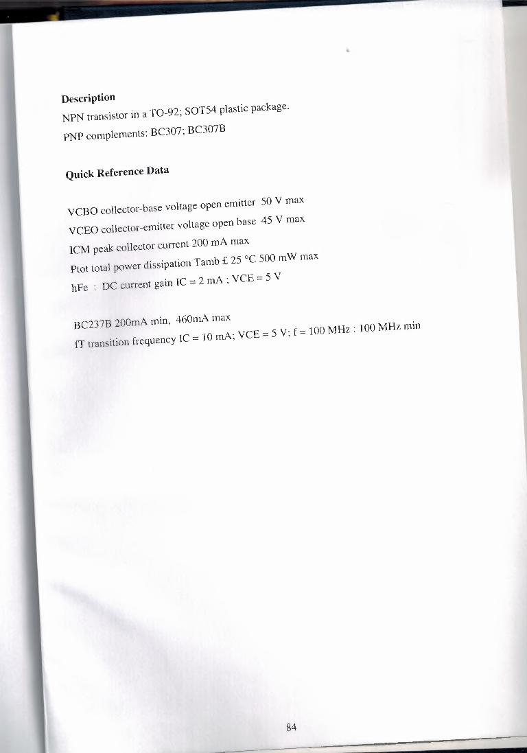
- Description NPN transistor in a T0-92; S0T54 plastic package.
PNP complements: BC307; BC307B
Quick Reference Data
VCBO collector-base voltage open emitter 50 V max
VCEO collector-emitter voltage open base 45 V max
ICM peak collector current 200 mA max
Ptot total power dissipation Tamb £ 25 °C 500 mW max
hFe : DC current gain IC == 2 mA ; VCE == 5 V
BC237B 200mA min, 460mA max IT transition frequency IC== 10 mA; VCE == 5 V; f == 100 MHz: 100 MHz min
84