networking behavior in thin film and nanostructure growth ... · networking behavior in thin film...
TRANSCRIPT

Networking Behavior in Thin Film and NanostructureGrowth Dynamics
Murat YukselUniversity of Nevada - Reno
Reno, NV 89557, [email protected]
Tansel KarabacakUniversity of Arkansas
Little Rock, AR 72204, [email protected]
Hasan GucluLos Alamos National Lab
Los Alamos, NM 87545, [email protected]
ABSTRACTThin film coatings have been essential in development ofseveral micro and nano-scale devices. To realize thin filmcoatings various deposition techniques are employed, eachyielding surface morphologies with different characteristicsof interest. Therefore, understanding and control of the sur-face growth is of great interest. In this paper, we devisea novel network-based modeling of the growth dynamics ofsuch thin films and nanostructures. We specifically map dy-namic steps taking place during the growth to components(e.g., nodes, links) of a corresponding network. We presentinitial results showing that this network-based modeling ap-proach to the growth dynamics can simplify our understand-ing of the fundamental physical dynamics such as shadowingand re-emission effects.
Categories and Subject DescriptorsH.1 [Models and Principles]: Miscellaneous; I.6 [Simulationand Modeling]: Model Development; C.2.1 [Computer-Communication Networks]: Network Architecture andDesign—network topology, network communications
1. INTRODUCTIONThin film coatings have been the essential components
of various devices in industries including microelectronics,optoelectronics, detectors, sensors, micro-electro-mechanicalsystems (MEMS), and more recently nano-electro-mechanicalsystems (NEMS). These coatings have thicknesses typicallyin the nano- to micro-scales and are grown using vacuum de-position techniques [2]. Thin film surface morphology con-trols many important physical and chemical properties ofthe films. It is therefore of great interest to understand andcontrol the development of the surface morphology duringthin film growth.
Commonly employed deposition techniques are thermalevaporation, sputter deposition, chemical vapor deposition(CVD), and oblique angle deposition. Different than oth-ers, oblique angle deposition technique [7] is typically used
Permission to make digital or hard copies of all or part of this work forpersonal or classroom use is granted without fee provided that copies arenot made or distributed for profit or commercial advantage and that copiesbear this notice and the full citation on the first page. To copy otherwise, torepublish, to post on servers or to redistribute to lists, requires prior specificpermission and/or a fee.Proceedings of Second International Conference on Nano-Networks ISBN 978-963-9799-03-5 Catania, Sicily, Italy, Septem-ber 24-26, 2007Copyright 2007 ACM ...$5.00.
for the growth of nanostructured arrays of rods and springsthrough a physical self-assembly process. In many applica-tions, it is often desired to have atomically flat thin filmsurfaces. However, in almost all of the deposition tech-niques mentioned above, the surface morphology generatesa growth front roughness. The formation of growth front isa complex phenomenon and very often occurs far from equi-librium. When atoms are deposited on a surface, atoms donot arrive at the surface at the same time uniformly acrossthe surface. This random fluctuation, or noise, which is in-herent in the process, may create the surface roughness. Thenoise competes with surface smoothening processes, such assurface diffusion (hopping), to form a rough morphology ifthe experiment is performed at either a sufficiently low tem-perature or a high growth rate.
A conventional statistical mechanics treatment cannot beused to describe this complex phenomenon. About twodecades ago, a dynamic scaling approach [6, 5] was proposed to describe the morphological evolution of a growthfront. Since then, numerous modeling and experimentalworks have been reported based on this dynamic scalinganalysis [2]. On the other hand, there has been a significantdiscrepancy among the predictions of these growth modelsand the experimental results published [9]. Briefly, theoret-ical predictions of growth models in dynamic scaling the-ory basically fall into two categories. One involves varioussurface smoothing effects, such as surface diffusion. Theother category involves the shadowing effect (which origi-nates from the preferential deposition of obliquely incidentatoms on higher surface points and always occurs in sputter-ing and CVD) during growth. However, experimentally re-ported values of growth exponent (which measures how fastthe root-mean-square roughness of the surface evolves as afunction of time according to a power-law relation) are farfrom agreement with the predictions of these growth models.Especially, sputtering and CVD techniques are observed toproduce morphologies ranging from very small to very largegrowth exponent values.
Understanding the thin film and nanostructure growthdynamics under the above-mentioned deposition techniqueshas been of high importance. There have been several stud-ies revealing fundamental dynamic effects (e.g., shadowing,re-emission, surface-diffusion, and noise effects) taking placeduring the growth process. Studies towards explaining thegrowth dynamics have been partly successful and only thesimulation-based studies were able to include all these ef-fects. In this paper, we devise a novel network-based mod-eling approach to better understand the growth dynamics.

Figure 1: Surface of a growing thin film (growthfront) under shadowing and re-emission effects.
We define a concise mapping between a network and the ba-sic physical operations taking place in the growth process.We, then, develop qualitative and quantitative understand-ing of the growth dynamics by studying the correspondingnetwork model. We present our initial results based on pre-viously recorded simulations of the growth process.
The rest of the paper is organized as follows: We startwith covering the thin film and nanostructure growth pro-cess and the basic physical effects involved in Section 2. Wethen survey the applications of dynamic network models onvarious areas in Section 3. Section 4 describes the details ofour methodology of mapping growth dynamics to a network.We present initial results of our network-based modeling ap-proach in Section 5, and conclude in Section 6.
2. BASICS OF THIN FILM AND NANOS-TRUCTURE GROWTH
Only recently, it has been recognized that in order tobetter explain the dynamics of surface growth one shouldconsiders the effects of both “shadowing” and “re-emission”processes [8]. As shown in Figure 1, particles can approachthe surface at oblique angles and be captured by higher sur-face points (hills) due to the shadowing effect. This leads tothe formation of rougher surfaces with columnar structuresthat can also be engineered to form “nanostructures” un-der extreme shadowing conditions, as in the case of obliqueangle deposition that can produce arrays of nanorods andnanosprings [7]. In addition, depending on the detailed de-position process, particles can either stick to or bounce offfrom their impact points, which is determined by a stick-ing probability, also named “sticking coefficient” (s). Non-sticking particles are re-emitted and can arrive at other sur-face points including shadowed valleys. In other words, re-emission has a smoothening effect while shadowing tries toroughen the surface. Both the shadowing and re-emissioneffects have been proven to be dominant over the surfacediffusion and noise, and act as the main drivers of the dy-namical surface growth front [7]. The prevailing effects ofshadowing and re-emission rely on their “non-local” char-acter: The growth of a given surface point depends on theheights of near and far-away surface locations due to shad-owing and existence of re-emitted particles that can travelover long distances.
Due to the complexity of the shadowing and re-emissioneffects, no growth model has been developed yet within theframework of dynamical scaling theory that take into boththese effects and still that can be analytically solved to pre-dict the morphological evolution of thin film or nanostruc-ture deposition. A dynamic growth equation that was pro-
posed by Drotar et al. [4] and developed for plasma and re-active ion etching processes (where in etching surface atomsare removed instead of being incorporated to the surfaceas in the case of deposition) that take into the re-emissionand shadowing effects could only be solved numerically fora limited case of re-emission and shadowing scenarios. Onlyrecently, shadowing and re-emission effects could be fullyincorporated into the Monte Carlo lattice simulation ap-proaches [9, 8, 4].
3. DYNAMIC NETWORK MODELSThe study of complex networks pervades various areas
of science ranging from sociology to statistical physics [3].A network in terms of modeling can be defined as a setnodes with links connecting them. Examples of real lifecomplex networks include the Internet, the World WideWeb, metabolic networks, transportation networks, socialnetworks, etc. Recent works, motivated by a large num-ber of natural and artificial systems, such as the ones listedabove, have turned the focus onto processes on networks,where the interaction and dynamics between the nodes arefacilitated by a complex network. Here, our aim is to con-struct the network from the apparent dynamics.
By using network-based modeling, fundamental under-standing of many natural and artificial systems has beenattained. In complex networks research, two major typesof network models are used for various applications: Small-world [10] and scale-free (power-law) [1] networks. Wattsand Strogatz, inspired by a sociological experiment, haveproposed a network model known as the small-world (SW)network, which means that, despite their often large size,there is a relatively short path between any two nodes inmost networks with some degree of randomness. The SWnetwork was originally constructed as a model to interpolatebetween regular lattices and completely random networks.Systems and models (with well known behaviors on regu-lar lattices) have been studied on SW networks, such as theIsing model, phase ordering, the Edwards-Wilkinson model,diffusion, and resistor networks.
The other major type of network is based on an observa-tion made in the context of real networks such as the Inter-net, World Wide Web, scientific collaboration network, ande-mail network. The common characteristic among thesenetworks is that they all exhibit power-law degree (connec-tivity) distributions. These networks are commonly knownas power-law or scale-free networks [1] since their degreedistributions are free of scale (i.e., not a function of thenumber of nodes N) and follow power-law distributions overmany orders of magnitude. This phenomenon has been rep-resented by the probability of having nodes with k degreesas P (k) ∼ k−γ where γ is usually between 2 and 3. Theorigin of the scale-free behavior can be traced back to twomechanisms that are present in many systems, and have astrong impact on the final topology. First, networks are de-veloped by the addition of new nodes that are connected tothose already present in the system. This mechanism signi-fies continuous expansion in real networks. Second, there isa higher probability that a new node is linked to a node thatalready has a large number of connections. With appropri-ate mapping to a network model, both of these mechanismscan be qualitatively shown in thin film and nanostructuregrowth dynamics. If we consider the thin film surface asa set of nodes and re-emissions as the links between them,

Figure 2: Identification of network “nodes” in a gridnetwork model corresponding to a landscape of agrowing thin film.
Figure 3: Grid network model development in space:Consider two, red and green, particles falling on agrowing thin film sample. The red particle makesfour re-emissions while the green one makes threere-emissions. We model each re-emission as a “link”between the nodes corresponding to the starting andending points of the re-emission.
the first mechanism refers to the understanding that eachparticle gets “connected” to the grid network by falling onto the film surface. Similarly, the second mechanism refersto that a falling particle will more likely to land on a large-size node thereby contributing to the scale-free topologicalbehavior of the growth dynamics.
4. MAPPING GROWTH DYNAMICS TO ANETWORK MODEL
Interestingly, non-local interactions among the surface pointsof a growing thin film that originate from shadowing and re-emission effects can lead to non-random preferred trajecto-ries of atoms/molecules before they finally stick and get de-posited. For example, during re-emission, the path betweentwo surface points where a particle bounces off from the firstand head on to the second can define a “network link” be-tween the two points. If the sticking coefficient is small, thenthe particle can go through multiple re-emissions that formlinks among many more other surface points. In addition,due to the shadowing effect, higher surface points act as thelocations of first-capture and centers for re-emitting the par-ticles to other places. In this manner, hills on a growing filmresembles to the network “nodes” of heavy traffic, where thetraffic is composed by the amount of re-emitted particles.
Several issues need to be considered in making a usefuland appropriate mapping between the growth dynamics ofthin films and nanostructures to a network modeling frame-work. Let us consider a snapshot of a growing thin film’slandscape. In Figure 2(a), let us say that blue color showscurrently elevated (i.e. hills) regions of the film and yel-low color shows currently not elevated (i.e. valleys) regionsof the film. The first mapping issue is to define a “node”in the corresponding network model. That is, what shouldbe the boundary of the corresponding network node on thethin film surface? Intuitively, each blue or yellow region in
Figure 4: Some basic processes in the simulation:(1) A particle is sent towards surface with angles θand φ based on an angular distribution chosen basedon the deposition technique. This particle sticks tothe surface with probability s0. (2) If it does notstick, then it is re-emitted after which it may findanother surface feature and stick there with proba-bility s1. This re-emission process continues like thisfor higher-order particles, too. (3) An adatom candiffuse on the surface. (4) Some surface points areshadowed from the incident and re-emission fluxes ofparticles due to the nearby higher surface features.
Figure 2(a) should ideally get mapped to a network node.However, this depends on the resolution of the grid beingused for developing a network model. If the grid resolutionis too fine, then a blue/yellow region of the film can corre-spond to multiple nodes as in Figure 2(b). Conversely, if thegrid resolution is too coarse, then multiple blue/yellow re-gions can correspond to one network node as in Figure 2(c).Having finer grid is more likely to capture dynamics of thegrowth; therefore, we will develop our network models in asfine granularity as possible. For a fine granularity networkmodel, it is always possible to aggregate the data pertainingto neighboring nodes and observe the behavior at coarsergranularity. This is illustrated in Figure 3, where the gridnetwork model can be developed at various scales in space.
After fixing the placement of nodes on the thin film, wethen map growth dynamics to components of the corre-sponding grid network model as shown in Figure 3. In gen-eral, we argue that we can make an analogy that hills andvalleys are nodes of the network system, but hills act asdistributing centers, and valleys as gathering centers due tothe shadowing and re-emission effects, respectively. The re-emissions of particles can, then, be modeled as a “link” fromthe re-emission’s starting node to the re-emission’s endingnode. The time it takes for the particle to reach to its newpoint can be considered as the link’s “propagation delay”,which implicitly expresses the distance between the startingand the ending nodes of the re-emission. It is even possi-ble to consider the link’s “capacity” as the highest possiblenumber of particles that can simultaneously travel from thestarting and the ending nodes of the re-emission, which islimited by the physical space corresponding to the link andaverage size of the re-emitting particles.
Since it is not possible to experimentally track the tra-jectories of re-emitted and deposited atoms during dynamicthin film growth, we will use Monte Carlo simulation ap-proaches instead that were already shown to efficiently mimicthe experimental processes and correctly predict the dy-

Figure 5: Top view images of simulated thin filmsurfaces grown under shadowing, re-emission, andnoise effects for sticking coefficients (a) s = 0.9 and(b) s = 0.1. Corresponding projected trajectories ofthe re-emitted particles are also mapped on the topview morphologies for (c) s = 0.9 and (d) s = 0.1.
namic growth morphology. In these simulations, each in-cident particle (e.g., atom or molecule) is represented withthe dimension of one lattice point. A specific angular distri-bution for the incident flux of particles is chosen dependingon the deposition technique being simulated. At each sim-ulation step, a particle is sent toward a randomly chosenlattice point on the substrate surface. Depending on thevalue of sticking coefficient s, the particle can bounce offand re-emit to other surface points. At each impact stick-ing coefficient can have different values represented as sn,where n is the order of re-emission (n = 0 being for thefirst impact)1. In all the emission and re-emission processesshadowing effect is included, where the particle’s trajectorycan be cut-off by long surface features on its way to othersurface points. After the incident particle is deposited ontothe surface, it becomes a so called “adatom”. Adatoms canhop on the surface according to some rules of energy, whichis a process mimicking the surface diffusion. This simula-tion steps are repeated for other particles being sent ontothe surface. Figure 4 illustrates the basic growth processesincluded in a typical Monte Carlo simulation approach.
5. INITIAL RESULTSIn order to explore existence of such a network behavior
during thin film and columnar nanostructure growth, we de-veloped 3D Monte Carlo simulations that take into shadow-ing, re-emission, surface diffusion, and noise effects. Theseeffects simulate the evolution of surface topography and alsothe simulation environment allows us to record the trajec-tories of re-emitted atoms. As an example, Figure 5 showsthe snapshot top view images of two surfaces simulated for aCVD type of deposition, at two different sticking coefficients.
1In this paper we assume a constant sticking coefficient forall subsequent re-emissions.
Figure 6: First row: Top view images from the sim-ulated thin film surfaces for a CVD growth withs = 0.9 at different film thicknesses d. Bottomrow: Corresponding projected trajectories of there-emitted particles qualitatively show the dynamicchange in the network topography.
Figure 5 also displays their corresponding particle trajecto-ries projected on the lateral plane. Qualitative network be-havior can easily be realized in these simulated morphologiesas the trajectories of re-emitted atoms “link” various surfacepoints. It can also be seen that larger sticking coefficients(Figure 5(a) and Figure 5(c)) leads to fewer but longer rangere-emissions, which are mainly among the peaks of colum-nar structures. Therefore, these higher surface points actas the “nodes” of the system. This is due to the shadow-ing effect where initial particles preferentially head on hills.They also have less chance to arrive down to valleys becauseof the high sticking probabilities (see also particle A illus-trated in Figure 1). On the other hand, at lower stickingcoefficients (Figure 5(b) and Figure 5(d)), particles now gothrough multiple re-emissions and can link many more sur-face points including the valleys that normally shadowed byhigher surface points (e.g. particle B in Figure 1).
Another interesting observation revealed in our MonteCarlo simulations was the dynamic change of network behav-ior on the trajectories of re-emitted particles. Figure 6 showstop view images and their corresponding particle trajecto-ries obtained from the simulations for a sticking coefficientof s = 0.9, but this time at different film thicknesses thatis proportional to the growth time. The dynamic changein the network topography can be clearly seen: at initialtimes, when the hills are smaller and more closely spaced,the re-emitted particles travel from one hill to another oneor to a valley. However, as the film gets thicker, and somehills become higher than the others and get more separated,particles travel longer ranges typically among these grow-ing hills. The shorter hills that get shadowed become thevalleys of the system. It is expected that this dynamic be-havior should be strongly dependent on the values of stickingcoefficients and angular distribution of the incident flux ofparticles, which determine the strength of re-emission andshadowing effects, respectively. In other words, each de-position technique and material system can have differentdynamic network behavior that can lead to various kinds ofnetwork systems.
0 10 20 30 40
k10
-6
10-4
10-2
100
P(k
)
s=0.1, d=6s=0.1, d=32s=0.1, d=71s=0.1, d=123s=0.9, d=44s=0.9, d=225s=0.9, d=497s=0.9, d=866
Degree Distributions (Undirected)
0 5 10 15 20 25 30
kin
10-6
10-4
10-2
100
P(k
in)
s=0.1, d=6s=0.1, d=32s=0.1, d=71s=0.1, d=123s=0.9, d=44s=0.9, d=225s=0.9, d=497s=0.9, d=860
Degree Distributions (In-degree)
0 5 10 15 20
In degree0
5
10
15
20
Ave
rage
Out
deg
ree
s=0.1, d=6s=0.1, d=32s=0.1, d=71s=0.1, d=123s=0.9, d=44s=0.9, d=225s=0.9, d=497s=0.9, d=860
In and Out Degree Correlations
100
101
102
103
l
10-6
10-4
10-2
100
P(l
) s=0.1, d=6s=0.1, d=32s=0.1, d=71s=0.1, d=123s=0.9, d=44s=0.9, d=225s=0.9, d=497s=0.9, d=860
Distance Distributions
(a) (b) (c) (d)
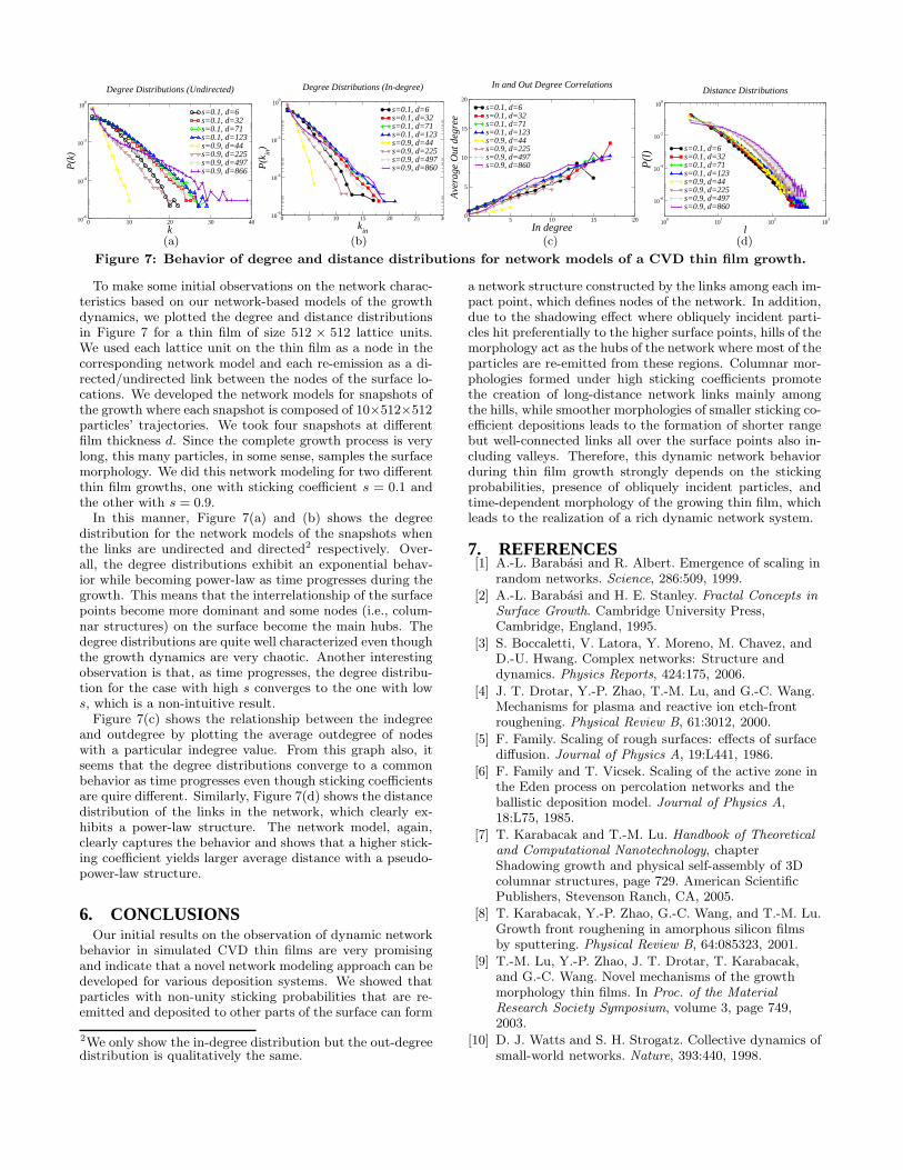
Figure 7: Behavior of degree and distance distributions for network models of a CVD thin film growth.
To make some initial observations on the network charac-teristics based on our network-based models of the growthdynamics, we plotted the degree and distance distributionsin Figure 7 for a thin film of size 512 × 512 lattice units.We used each lattice unit on the thin film as a node in thecorresponding network model and each re-emission as a di-rected/undirected link between the nodes of the surface lo-cations. We developed the network models for snapshots ofthe growth where each snapshot is composed of 10×512×512particles’ trajectories. We took four snapshots at differentfilm thickness d. Since the complete growth process is verylong, this many particles, in some sense, samples the surfacemorphology. We did this network modeling for two differentthin film growths, one with sticking coefficient s = 0.1 andthe other with s = 0.9.
In this manner, Figure 7(a) and (b) shows the degreedistribution for the network models of the snapshots whenthe links are undirected and directed2 respectively. Over-all, the degree distributions exhibit an exponential behav-ior while becoming power-law as time progresses during thegrowth. This means that the interrelationship of the surfacepoints become more dominant and some nodes (i.e., colum-nar structures) on the surface become the main hubs. Thedegree distributions are quite well characterized even thoughthe growth dynamics are very chaotic. Another interestingobservation is that, as time progresses, the degree distribu-tion for the case with high s converges to the one with lows, which is a non-intuitive result.
Figure 7(c) shows the relationship between the indegreeand outdegree by plotting the average outdegree of nodeswith a particular indegree value. From this graph also, itseems that the degree distributions converge to a commonbehavior as time progresses even though sticking coefficientsare quire different. Similarly, Figure 7(d) shows the distancedistribution of the links in the network, which clearly ex-hibits a power-law structure. The network model, again,clearly captures the behavior and shows that a higher stick-ing coefficient yields larger average distance with a pseudo-power-law structure.
6. CONCLUSIONSOur initial results on the observation of dynamic network
behavior in simulated CVD thin films are very promisingand indicate that a novel network modeling approach can bedeveloped for various deposition systems. We showed thatparticles with non-unity sticking probabilities that are re-emitted and deposited to other parts of the surface can form
2We only show the in-degree distribution but the out-degreedistribution is qualitatively the same.
a network structure constructed by the links among each im-pact point, which defines nodes of the network. In addition,due to the shadowing effect where obliquely incident parti-cles hit preferentially to the higher surface points, hills of themorphology act as the hubs of the network where most of theparticles are re-emitted from these regions. Columnar mor-phologies formed under high sticking coefficients promotethe creation of long-distance network links mainly amongthe hills, while smoother morphologies of smaller sticking co-efficient depositions leads to the formation of shorter rangebut well-connected links all over the surface points also in-cluding valleys. Therefore, this dynamic network behaviorduring thin film growth strongly depends on the stickingprobabilities, presence of obliquely incident particles, andtime-dependent morphology of the growing thin film, whichleads to the realization of a rich dynamic network system.
7. REFERENCES[1] A.-L. Barabasi and R. Albert. Emergence of scaling in
random networks. Science, 286:509, 1999.
[2] A.-L. Barabasi and H. E. Stanley. Fractal Concepts inSurface Growth. Cambridge University Press,Cambridge, England, 1995.
[3] S. Boccaletti, V. Latora, Y. Moreno, M. Chavez, andD.-U. Hwang. Complex networks: Structure anddynamics. Physics Reports, 424:175, 2006.
[4] J. T. Drotar, Y.-P. Zhao, T.-M. Lu, and G.-C. Wang.Mechanisms for plasma and reactive ion etch-frontroughening. Physical Review B, 61:3012, 2000.
[5] F. Family. Scaling of rough surfaces: effects of surfacediffusion. Journal of Physics A, 19:L441, 1986.
[6] F. Family and T. Vicsek. Scaling of the active zone inthe Eden process on percolation networks and theballistic deposition model. Journal of Physics A,18:L75, 1985.
[7] T. Karabacak and T.-M. Lu. Handbook of Theoreticaland Computational Nanotechnology, chapterShadowing growth and physical self-assembly of 3Dcolumnar structures, page 729. American ScientificPublishers, Stevenson Ranch, CA, 2005.
[8] T. Karabacak, Y.-P. Zhao, G.-C. Wang, and T.-M. Lu.Growth front roughening in amorphous silicon filmsby sputtering. Physical Review B, 64:085323, 2001.
[9] T.-M. Lu, Y.-P. Zhao, J. T. Drotar, T. Karabacak,and G.-C. Wang. Novel mechanisms of the growthmorphology thin films. In Proc. of the MaterialResearch Society Symposium, volume 3, page 749,2003.
[10] D. J. Watts and S. H. Strogatz. Collective dynamics ofsmall-world networks. Nature, 393:440, 1998.