neural-based microwave modeling and...
TRANSCRIPT

1
Neural Networks for Microwave Modeling and Design
Humayun Kabir, Lei Zhang, Ming Yu, Peter H. Aaen, John Wood, and Qi-Jun Zhang
Modeling and computer-aided design (CAD) techniques are essential for microwave design, especially with our drive towards first-pass design success. In the past few decades, tremendous progress in microwave CAD has led to a large variety of microwave models for passive and active devices and circuit components. The high quality and the availability of these models have enabled us to design circuits efficiently. These models have also allowed us to design larger and more complicated circuits than ever before.
At the same time, new technologies and materials, emerging and non-traditional devices continue to evolve. Although the existing models are good for modeling mature technologies and existing devices, they are often inadequate or unsuitable when new devices are needed in system design. Conventional approaches to create or modify models are heavily based on slow trial-and-error processes. As new technologies and devices continue to evolve, we need not only new models, but also computer-aided modeling algorithms such that model development becomes fast and systematic.
At high frequencies, equivalent circuit models often lack fidelity. Detailed electromagnetic (EM) based simulations become essential to achieve design accuracy. However, EM simulations are computationally expensive especially when physical or geometrical parameters have to be repeatedly adjusted during design cycle. With the increasing design complexities, coupled with tighter component tolerances and shorter design cycles, there is a demand for design methodologies that are both accurate and fast at the same time. These are contradictory requirements and difficult to satisfy with conventional CAD techniques. The problem becomes even more severe in yield optimization and statistical validation where process variations and manufacturing tolerances of components are required to be taken into account. In addition, accurate parametric modeling techniques have become increasingly necessary, where we strive to describe not only the behavior of the microwave device, but also the change of the behavior against physical or geometrical parameters of the device.
In recent years, neural network (NN) or artificial neural network (ANN) techniques have
been recognized as a useful alternative to conventional approaches in microwave modeling [1]-[2]. Artificial neural networks can be used to develop new models or to enhance the accuracy of existing models. Neural networks learn device data through an automated training process, and the trained neural networks are then used as fast and accurate models for efficient high-level circuit and system design. These models have the ability to capture multi-dimensional arbitrary nonlinear relationships. The theoretical basis of neural network is based on the universal approximation theory [3], which states that a neural network with at least one hidden layer can approximate any nonlinear continuous multidimensional function to any desired accuracy. This makes neural networks a useful choice for device modeling where a mathematical model is not available. The evaluation from input to output of a neural network model is also very fast. For these reasons, neural network techniques have been utilized in various microwave design applications [1]-[2], [4]-[5] such as vias and interconnects [6], embedded passives [7]-[8], coplanar wave-guide components [9]-[11], parasitic modeling [12], antenna applications [13]-[15], nonlinear microwave circuit optimization [16]-[18], nonlinear device modeling [19]-[22], power amplifier modeling [23]-[26], waveguide filter [27]-[29], enhanced EM computation [30], etc. In this article, we present an overview of neural network -based modeling techniques and their applications in microwave modeling and design. Basics of Neural Networks Neural networks are information processing systems with their design inspired by the studies of the ability of the human brain to learn from observations and to generalize by abstraction [1]. A typical neural network structure is comprised of two types of basic components: the processing elements and the interconnections between them [2]. The processing elements are called neurons and the connections between the neurons are known as links or synapses. Every link has a corresponding weight parameter associated with it. Each neuron receives stimuli from other neurons connected to it, processes the information, and produces an output. Neurons that receive stimuli from outside the network are called input neurons while neurons whose outputs are

2
externally used, are called output neurons. Neurons that lie between input and output neurons are termed as hidden neurons. Different neural network structures are constructed by using different types of neurons and by connecting them differently. Multilayer perceptrons (MLP) is a popularly used neural network structure. In the MLP neural network, the neurons are grouped into layers. For example in a three-layer perceptron, the first layer is the input layer, the second layer is hidden layer, and the third layer is the output layer, as indicated in Figure 1. Figure 1. Multilayer perceptrons neural network structure. Typically, a multilayer perceptron network consists of an input layer, one or more hidden layers, and an output layer [2]. In the MLP network, each neuron processes the stimuli (inputs) received from other neurons. The process is done through a function called activation function in the neuron, and the processed information becomes the output of the neuron. Let x be a vector, of size 1 x n, representing inputs to the neural network (e.g., gate length and width of a FET). Let y be a vector, of size 1 x m, representing the outputs from the neural network (e.g., various responses of the device). The output of a three-layer neural network is computed as
(2)(2)0
1
q
h hjj jh
wy z w (1)
where, j = 1, 2,…, m, zh is the output of the h
th
hidden neuron computed as
(1)(1)0
1
1;
1 hh
n
i ihh hi
ze
x w w
, (2)
where h = 1, 2,…, q, q is the number of hidden
neurons, (1)
ihw is the weight parameter linking the
ith input and h
th neuron in the hidden layer,
(2)
hjw is
the weight parameter linking the hth neuron in the
hidden layer and jth neuron in the output layer, and
(2)
0 jw and (1)
0hw are bias values for the jth output
neuron and the hth hidden neuron, respectively.
The process for computing y from inputs x is as follows: The external inputs x are applied to the input neurons (i.e., the first layer) and they become the stimuli for the hidden neurons of the second layer. For each hidden neuron, the sum of the weighted stimuli (which is λh in (2)) is used to trigger the activation function (the sigmoid function in (2)) producing the response zh for the hidden neuron. Continuing this way, the response from second layer neurons become stimuli for the output layer neurons (i.e., the third layer). For each output neuron, the sum of the weighted stimuli becomes the response of the output neuron. This process is called the feedforward computation process, which is required during training or model evaluation. In feedforward computation, neural network weights w which contain all the weight and bias parameters
(1)
ihw ,(2)
hjw ,(1)
0hw ,(2)
0 jw , i = 1, 2, …, n, j = 1, 2, …, m,
and h = 1, 2, …, q, remain fixed. The most important step in neural network
model development is the neural network training. Let dk be the k
th sample of y in training data. We
define neural network training error as,
2
1
1( ) ( , )
2rr
m
T j k jkk T j
E y x w d
w (3)
where djk is the j
th element of data vector dk ,
( )j ky x ,w is the jth neural network output for input
kx , Tr is the index set of all training data, and
w is the vector of neural network weight
parameters. The purpose of neural network training, in basic terms, is to adjust w such that the error
function ( )rTE w is minimized. Since ( )
rTE w is a
nonlinear function of the adjustable (i.e., trainable) weight parameters w , iterative algorithms are
x1 x2 x3
1 2 3 n
1 2 3 q
1
y1 y2 ym
2 m Layer 3
(Output layer)
Layer 2 (Hidden layer)
Layer 1
(Input layer)
xn
w(2)
w(1)

3
often used to explore the w-space efficiently, i.e. beginning with an initialized value of w and then
iteratively updating it. During training, the error between data and the neural network outputs are propagated starting from the output layer, through the hidden layer and ending at the input layer. In this process, the derivative information of the training error with respect to the weight parameters in each layer is computed. This information is used either directly to update the value of each weight parameter in the neural network (Backpropagation training algorithm [31]), or as gradient information for gradient based algorithms such as conjugate gradient or quasi-Newton [2], [32]. Global optimization algorithms, such as genetic algorithms and particle swarm optimization [33] have also been used to improve the quality of training at the cost of long training time. Using suitable functions (such as sigmoid) as the activation functions in the hidden layer as described in (2), the derivative of an activation function can be obtained without additional cost once the activation function is evaluated. To obtain the optimal neural network, hidden neurons can be successively added to the network and the network is trained until the best error estimate is obtained. Another approach involves training a neural network that contains a larger number of neurons than required; pruning techniques are then used to remove unnecessary neurons. One of the goals of the training is to obtain a network that is capable of ‘generalization’: the ability to predict the correct output for input data that was not used in the training dataset. This is essentially what we require from the function approximation of discrete measured data. Training techniques for improving the generalization of a neural network include ‘early-stopping’ using cross-validation, in which different subsets of the measured data are used for training and validation, with the validation being carried out periodically during the training to assess whether a suitable minimum in the error surface has been reached [34]. Automated model generation algorithms have also been developed including adjustment of the number of hidden neurons, adaptive sampling (of training data), and training data generation as a part of the overall training process [7]. A neural network can be viewed as a general, parameterized, nonlinear mapping between a set of input variables and a set of output variables (or data). As a comparison, conventional approximation methods such as polynomials or rational functions can also achieve such mapping
provided that there are enough terms in the approximation, that is, the polynomial is of sufficiently high in degree. For a polynomial of degree M, the number of free parameters for a space having dimensionality n is proportional to n
M [34]. Therefore, to achieve a high accuracy in a
multi-dimensional space, a large number of free parameters must be determined. The greater the numbers of dimensions, the more the free parameters are required. This means an increased complexity of the polynomial, increased memory requirement for coefficient storage, and reduced computational efficiency of the function evaluation. This problem is known as the curse of dimensionality. One of the most significant advantages of neural networks as a function approximation technique lies in the manner in which they deal with this problem of scaling with dimensionality. Since the functions of the neural network are adapted as a part of the training process, the number of functions has to be increased only when the complexity of the problem increases, not simply because the dimensionality of the problem grows. For neural networks, the number of free parameters typically grows only linearly or quadratically with the dimensionality of the input space. Therefore, for multi-dimensional function approximation, neural networks have significant advantages over other techniques, as they permit a compact representation of a multi-dimensional function, requiring minimal storage of coefficients and being very efficient to evaluate [34]. General Neural Network Modeling Approach The idea of neural network modeling is to use the simple formulas described by (1) and (2) to approximate multidimensional nonlinear relations between x and y. By simply adding input neurons, it can deal with multidimensional input variables (x) much more easily than polynomial, rational or table models. By adding more hidden neurons, it can handle arbitrary nonlinearity between x and y more efficiently than other approximation approaches.
In order to develop a neural network model, we first define the input and output variables of the device or structure. We then generate input-output data using EM simulation, physics-based simulation or measurement. The data, called training data, are used to train the neural network. Once the model is developed, it can be incorporated into a circuit simulator for fast and accurate simulation and optimization [35]-[38]. This allows circuit level simulation speed with electromagnetic level accuracy. This process is

4
illustrated in Figure 2. For a given component, in this example a spiral inductor, training data are generated using EM simulation for a range of physical and geometrical parameters (that is, for a range of width W, spacing LS, dielectric
constantr ). These data are used to train a neural
network. The trained neural network is then incorporated into a circuit simulator. It enables fast simulation and optimization of a circuit using the component (e.g., spiral inductor) as a part of the overall circuit. Because the model is parametric, the geometrical variables of this component can be adjusted during circuit simulation and optimization without having to re-do the original EM simulation. Note that the model is developed once and then can be reused for many different circuit optimizations.
Figure 2. Illustration of fast circuit optimization where a spiral inductor component is represented by a neural network model, avoiding repeated EM simulation when geometrical parameters are changed.
The neural network can also be combined with existing models to produce a parametric model. This is a part of the knowledge-based neural network concept, which exploits existing microwave knowledge in the form of empirical/analytical/equivalent model during neural network development. For example [39], in order to develop a fast parametric model for a transmission line, a neural network model was
first developed to relate , _r eff , and Zo to
physical/geometrical parameters. The inputs of the neural network are frequency, thickness of substrate, width and length of the line. The
outputs are , _r eff , and Zo. This information is
then fed to the transmission line equations to compute the S-parameters. The overall transmission line parametric model combines the neural network and the analytical formula as shown in Figure 3. The model response matches well with EM data as shown in Figure 4. The evaluation time for the model (including neural network and analytical formulas) is only a small fraction of that for EM simulation. The result of the model is used for higher level simulation, such as high-power transistor device package simulation, consisting of transmission lines, matching networks, etc [39].
Figure 3. A neural network model of a transmission line combining neural networks with analytical transmission line formulas. The overall model is parametric allowing fast evaluation of transmission line behavior with geometrical parameters as variables [39].
αα εεrr__eeffff ZZ00
freq width thickness length
……..
……..
Analytical Equation for Transmission Line
[S]
tanh(.)
tanh(.)
r
LWLS
r
LW
r
LWLS
Training data generation
using EM simulator
Neural network
model training
W LS r f
Circuit
Simulator
Fast optimization of
microwave circuit
using the spiral model
Incorporation into
circuit simulator
11
RS 11
IS 12
RS 12
IS

5
Figure 4. Comparison of the transmission line coefficients evaluated from the neural network model versus EM simulation. The transmission line model was verified for oxide layers 0.25 – 2 μm thick on top of 125 μm of silicon. The width of the transmission line was swept from 200 to 1500 μm [39]. Neural Network for Inverse Modeling Problem A neural network trained to model an original EM problem can be called the forward model where the model inputs are physical or geometrical parameters and outputs are electrical parameters (analysis). That is, for a given geometry or physical parameters, tell me the electrical parameters, using a 1-to-1 mapping. For the design purpose, the information is often processed in the reverse direction in order to find the physical or geometrical parameters for given values of electrical parameters, which is called the inverse problem. In other words, this is the reverse of analysis: from given electrical specifications find me the geometrical and device parameters that will provide me the description. There are two methods to solve the inverse problem, that is, the optimization method and the direct inverse modeling method. In the
optimization method, the EM simulator or the forward model is evaluated repeatedly in order to find the optimal solutions of the geometrical parameters that can lead to a good match between modeled and specified electrical parameters. This method of inverse modeling is also known as synthesis method [29]. Another method is to use an inverse model whose inputs are electrical parameters and outputs are geometrical parameters. An inverse model can provide geometrical parameters for a specific electrical specification in one evaluation. This method becomes faster than the optimization method.
The formula for the inverse problem, that is, compute the geometrical parameters from given electrical parameters, is difficult to find analytically. Therefore, the neural network becomes a logical choice since it can be trained to learn from the data of the inverse problem. We define the input neurons of a neural network to represent the electrical parameters of the modeling problem and the output neurons to represent the geometrical parameters.
After the formulation is finished, the model is trained with the data. Usually data are generated by EM solvers originally in a forward way, that is, geometrical parameters are given and electrical parameters are computed. To train the neural network inverse model, we swap the generated data so that electrical parameters become training data for neural network inputs and geometrical parameters become training data for neural network outputs. Using these data, the trained neural network becomes a direct inverse model. The model is then used to obtain values of geometrical design variables from an electrical parameter in a single model evaluation.
Unlike the forward model in which the input to output mapping (from geometrical parameter to electrical parameter) is usually a 1-to-1 mapping, the inverse model often encounters the problem of nonunique solutions. This problem also causes difficulties during training, because the same input values to the inverse model will lead to different values at the output (multivalued solutions). Consequently, the neural network inverse model cannot be trained accurately. This is why training an inverse model may become more challenging than training a forward model. A method has been recently introduced to address such a problem by detecting multivalued solutions in training data [28]. The data containing multivalued solutions are divided into groups according to derivative information using a neural network forward model, such that individual groups do not have the

6
problem of multivalued solutions. Multiple inverse models are built based on divided data groups, and are then combined to form a complete model [28]. Development of Neural Network Inverse Models for Waveguide Filter We develop neural network inverse models for waveguide filter. These inverse models will be used to design filters with the inverse approach. The filter is decomposed into three different modules, each representing a separate filter junction. The three models are the input-output (IO) iris, the internal coupling iris, and the tuning screws. Figure 5 shows a diagram of a waveguide filter revealing various dimensions of the models. Symbol M12 represents the coupling term between cavity 1 and cavity 2. Other coupling terms are also defined similarly.
Figure 5. Diagram of a circular waveguide filter showing various geometrical variables. M12 represents the coupling term between cavity 1 and cavity 2 [27].
The inverse coupling iris model was
formulated by swapping the vertical and horizontal coupling slot Lv and Lh with coupling terms M23 and M14. The inverse IO iris model was formulated such that iris length Lr becomes output and coupling R becomes input of the inverse model. The inverse tuning screw model was formulated by swapping tuning screw lengths LH and LC with coupling term M12 and phase P. Thus the filter dimensions which are the design variables become the output variables of the inverse model. Figure 6 presents the three inverse models showing the inputs and outputs of the three models. The ωo and CD represent center frequency and cavity diameter respectively.
EM simulations were performed and the resulting data were used to develop the inverse
models following the methodology presented in [28]. For IO iris and coupling iris model, good accuracy was achieved by using the segmentation method described above. For tuning screw model, segmentation, derivative division and model combining techniques were used to produce 99% accurate model. These models were developed using NeuroModelerPlus [40].
(a)
(b) (c)
Figure 6. Neural network inverse models representing junctions of a waveguide filter (a) Input-output (IO) iris model, (b) Internal coupling iris model, (c) Tuning screw model. Symbols CD and ωo represent cavity diameter and center frequency, respectively. The coupling terms R, M12, M23, M34, and M14 represent electrical coupling between various cavities of the waveguide. Symbols Lr, Lv, Lh, Lc, and LH represent geometrical dimensions of the filter. Symbols Pv, Ph, and Pin are the phase terms.
Waveguide Filter Design Using Inverse Models
In the conventional approach, the filter design starts from synthesizing the coupling matrix to satisfy ideal filter specifications. The EM method for finding physical/geometrical parameters to realize the required coupling matrix is an iterative EM optimization procedure. This procedure performs EM analysis (mode-matching or finite
Lr Pv Ph Pin
CD ωo R
Lr Pv Ph Pin
CD ωo R
Lr Pv Ph Pin
CD ωo R
Lr Pv Ph Pin
CD ωo R
CD ωo M23 M14
Lv Lh Pv Ph
CD ωo M23 M14
Lv Lh Pv Ph
CD ωo M23 M14
Lv Lh Pv Ph
CD ωo M12 P
Ph LH Lc
CD ωo M12 P
Ph LH Lc
CD ωo M12 P
Ph LH Lc
Lr
Lv, Lh
Lc
LH
M12

7
element methods) on each waveguide junction of the filter to get the generalized scattering matrix (GSM). From GSM we extract coupling coefficients. We then modify the design parameters (i.e., the dimensions of filter) and re-perform EM analysis iteratively until the required coupling coefficients are realized. The optimization process using a forward neural network model would speed up the process. However, the optimization process needs many iterations and it may suffer from convergence problems.
In Figure 7, we show the design approach using a neural network inverse model. We avoid the iterative step as well as obtain accurate result since the submodels are accurately trained. Note that the steps of generating ideal coupling matrix from specification are the same for both the conventional approach and the approach using inverse models. However, in the later approach the filter dimensions are obtained in one step using inverse models. This reduces design time significantly by avoiding repetitive model evaluations.
Figure 7. Design approach using advanced neural network inverse models [28].
A 6-pole Filter Design for Device Level Verification of the Inverse Methods
We present a 6-pole waveguide filter design following the inverse approach [28]. The filter’s center frequency is 12.155 GHz, bandwidth is 64 MHz and cavity diameter is chosen to be 1.072". The normalized ideal coupling values are obtained from coupling matrix synthesis as shown in Figure 7. The dimensions are then obtained from the inverse neural network models that were developed before. We then manufactured the filter
and tuned it by adjusting irises and tuning screws to match the ideal response. Figure 8 presents the response of the tuned filter and compares with the ideal one showing a perfect match between each other. The dimensions of the tuned filter are measured and compared with the dimensions obtained from the neural network inverse models. The neural network dimensions match the measurement dimensions very well. The quality of the solutions from the inverse neural networks is similar to that from the EM design, both being excellent starting points for final tuning of the filter. Moreover, the advantage of using the neural network inverse models is realized in terms of time compared to EM models. An EM simulator can be used for synthesis, which requires typically 10 to 15 iterations to generate inverse model dimensions. It takes approximately 6.5 minutes to obtain the filter dimensions using EM models whereas neural network inverse models provide the same result in less than a second.
-70
-60
-50
-40
-30
-20
-10
0
12.06 12.09 12.11 12.14 12.16 12.18 12.21 12.24 12.26
Frequency (GHz)
S11/S
21 (
dB
)
S11 ideal S21 ideal
S11 measurement S21 measurement
Figure 8. Comparison of the 6-pole filter response with ideal filter response. The filter was designed, fabricated, tuned and then measured to obtain the dimensions [28]. Neural Network for Parametric Modeling of a Complete Microwave Filter
A parametric model for a complete filter requires that the model has many geometrical variables. In conventional approach, change of a geometrical variable requires EM re-simulation of the whole filter. This is a slow process. Here, we develop a fast neural network model for this purpose. The geometrical variables will be formulated as neural network input neurons. Outputs of the neural network are S-parameters of the overall filter. Since there are many design variables involved, we require a high-dimensional neural network [41].
We describe the high dimensional neural network modeling through an example of
Coupling matrix
Synthesis
Filter Specification
Neural Inverse Model
for Filter
Ideal Coupling Values
Geometrical
Dimensions of the Filter

8
modeling a complex microwave filter known as side-coupled circular waveguide dual-mode filter [42], [43]. Figure 9 shows physical diagrams of the filter revealing major design variables. This type of filter offers significant performance improvement and finds its application in the satellite multiplexers with extremely stringent mass, size, and thermal requirements. However, the design and simulation become more difficult due to the structural complexity [43].
(b)
(c)
Figure 9. Diagram of a side-coupled filter (a) Side view, (b) Top view [41].
The filter contains 15 design variables
including 12 geometrical parameters, bandwidth, center frequency, and frequency. If conventional neural network approach is used to represent this 15-dimensional problem, i.e., 15 input neurons, data generation and neural network training would be a prohibitive process. Modular neural network is an approach where a set of simple neural networks work together to provide solution of a complex problem. Each of the simple neural networks represents a partial problem of the overall problem. Here we apply the modular concept to simplify the high-dimensional modeling problem into a set of low-dimensional modeling problems.
We decompose the filter into three types of substructures, named as input-output iris, internal coupling iris, and coupling and tuning screw [27], for which three neural network submodels are
developed. The inputs of the submodels are geometrical dimensions and outputs are coupling parameters. The number of input variables of each substructure is much less than that of the overall filter. This allows us to develop very accurate submodels inexpensively. The submodels were combined with filter equivalent circuit model to produce the approximate solution of the side-coupled filter. Since it is difficult to find an analytical formula to map the approximate solution to the accurate solution, we develop another neural network mapping model for this purpose. Figure 10 shows the diagram of the neural network model of the side coupled filter. Symbols Lr1 and Lr2 represent lengths of input iris and output iris, respectively, L11b1, L22b1, and L12b1 represent lengths of three screws of cavity 1, L11b2, L22b2, and L12b2 represent three screws of cavity 2, L23 represents length of the sequential coupling iris, L14 represents length of cross coupling iris, Lb1 and Lb2 represent lengths of cavity 1 and cavity 2, respectively, B represents bandwidth, ωo represents center frequency, and ω represents frequency. In Figure 10, R1 and R2 represent input and output coupling bandwidth, M11 to M44 are self coupling bandwidths, and M12, M23, M34, and M14 represent sequential and cross-coupling bandwidths.
Figure 10. Neural networks to develop a parametric model of a complete side-coupled filter. Three low-dimensional neural networks are combined with filter’s empirical/equivalent circuit models to produce approximate solution of the filter. A neural network mapping model then produces the accurate solution of the filter.
Modular neural networks representing models for IO iris, coupling iris, and
tuning screw
Neural network mapping model
Approximate solution
Accurate solution
1 2 11 22 33 44 12 23 34 14
TR R M M M M M M M M y
Input variables
1 2 11 1 22 1 12 1 23 14 11 2 22 2
12 2 1 2
[
]
r r b b b b b
T
b b b o
L L L L L L L L L
L L L B
x
Input/output irises
Coupling iris
Coupling screw
Tuning screws

9
In Figure 11, we plot responses of a side-coupled filter obtained from the neural network high dimensional model and EM model. It shows that the model can be used to obtain responses nearly as accurate as EM model. In Table 1, we list model evaluation time of two commonly used EM models and compare with the evaluation time of the high dimensional neural network model. Full EM simulation of the entire filter needs approximately 6 minutes using mode-matching based EM simulator [42] and 45 minutes using finite-element based EM simulator such as HFSS [44]. The comparison clearly shows that the high dimensional neural network model is significantly faster than the EM model enabling fast design and optimization.
Table 1. Comparison of CPU time of EM and neural network models of a side-coupled circular waveguide filter [41]
Modeling methods
Model evaluation
time
Finite Element Method 45 min
Mode Matching Method 6 min
Neural Network Method 0.6E-3 s
-80
-60
-40
-20
0
11.5 11.7 11.9 12.1 12.3 12.5
Frequency (GHz)
S1
1 (
dB
)
Neural-solution
EM-solution
(a)
Figure 11. Comparisons of reflection coefficients of a side-coupled circular waveguide dual-mode filter obtained using the neural network model and the EM model [41]. Neural Network for Correction of Nonlinear Device Models
Another useful application of neural network is to map or repair an existing model to match a new device. This process is called Neuro-Space Mapping (Neuro-SM) [45]-[46]. The starting point for the Neuro-SM is when the existing/available device model (coarse model) cannot match the data of a new device (fine model). Suppose that the gap between the coarse and fine models cannot be overcome by simply optimizing the
parameters in the coarse model. To achieve a model that can best match the device data, the model structure or the nonlinear equations of the coarse model need to be modified.
An example the Neuro-SM model is shown in Figure 12 for a HEMT device. The original data for the HEMT device is obtained from physics-based device simulator MINIMOS [47], which is a fine model. An existing HEMT model, the Angelov (Chalmers) Model [48], is used as the initial model (coarse model). After optimizing the internal parameters of the coarse model, we discovered that the gap between the optimized coarse model and the device data is still not easy to diminish.
(a)
(b)
Figure 12. (a) Physical structure of a HEMT device used for physics-based device simulator (fine model). (b) Neuro-SM HEMT intrinsic nonlinear model. The coarse model is an existing/available equivalent circuit model. The neural network mapping is incorporated as the controlling functions in the controlled sources [45].
In order to further improve the coarse model’s
accuracy, we will need to find a function that can map the coarse model behavior to the fine model behavior. However, the mapping function is difficult to derive analytically. For this reason, neural network becomes useful to obtain the required mapping. The neural network is trained to learn the relation between the coarse model
Coarse Model
vdc vgc
id=idc
vd
ig=igc
vg
Gate Signals:
fine coarse Drain Signals:
coarse fine
idc igc ig id
Mapping Neural Network
[vgc vdc]= fANN(vg,vd, w)
Source
Channel
(Undoped InGaAs)
Semi-insulating GaAs
Substrate
Undoped GaAs Buffer
Undoped AlGaAs
Gate
n+ GaAs n+ GaAs
δ-dopping
Drain
AlGaAs AlGaAs
10
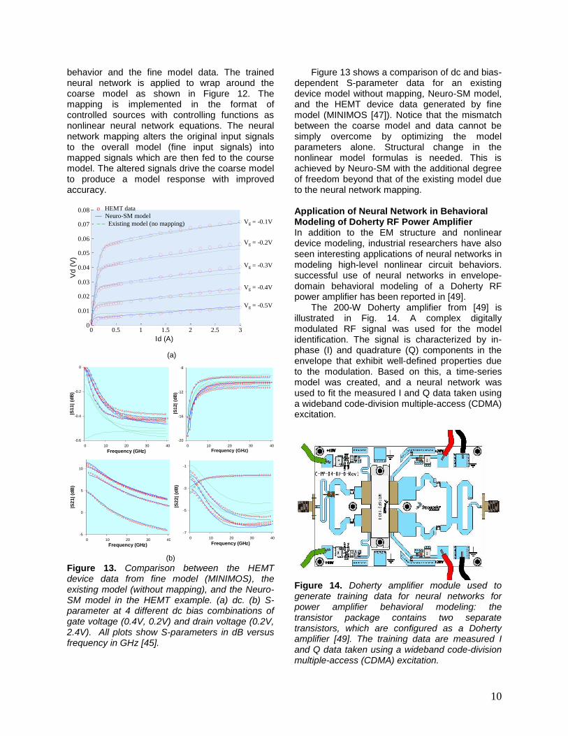
behavior and the fine model data. The trained neural network is applied to wrap around the coarse model as shown in Figure 12. The mapping is implemented in the format of controlled sources with controlling functions as nonlinear neural network equations. The neural network mapping alters the original input signals to the overall model (fine input signals) into mapped signals which are then fed to the course model. The altered signals drive the coarse model to produce a model response with improved accuracy.
0 0.5 1 1.5 2 2.5 30
0.01
0.02
0.03
0.04
0.05
0.06
0.07
0.08
Id (A)
Vd
(V
)
(a)
(b)
Figure 13. Comparison between the HEMT device data from fine model (MINIMOS), the existing model (without mapping), and the Neuro-SM model in the HEMT example. (a) dc. (b) S-parameter at 4 different dc bias combinations of gate voltage (0.4V, 0.2V) and drain voltage (0.2V, 2.4V). All plots show S-parameters in dB versus frequency in GHz [45].
Figure 13 shows a comparison of dc and bias-dependent S-parameter data for an existing device model without mapping, Neuro-SM model, and the HEMT device data generated by fine model (MINIMOS [47]). Notice that the mismatch between the coarse model and data cannot be simply overcome by optimizing the model parameters alone. Structural change in the nonlinear model formulas is needed. This is achieved by Neuro-SM with the additional degree of freedom beyond that of the existing model due to the neural network mapping. Application of Neural Network in Behavioral Modeling of Doherty RF Power Amplifier In addition to the EM structure and nonlinear device modeling, industrial researchers have also seen interesting applications of neural networks in modeling high-level nonlinear circuit behaviors. successful use of neural networks in envelope-domain behavioral modeling of a Doherty RF power amplifier has been reported in [49].
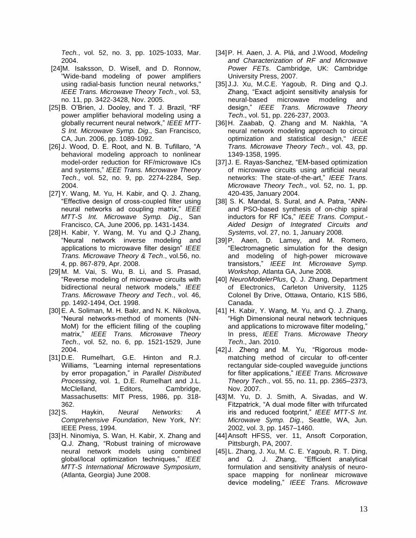
The 200-W Doherty amplifier from [49] is illustrated in Fig. 14. A complex digitally modulated RF signal was used for the model identification. The signal is characterized by in-phase (I) and quadrature (Q) components in the envelope that exhibit well-defined properties due to the modulation. Based on this, a time-series model was created, and a neural network was used to fit the measured I and Q data taken using a wideband code-division multiple-access (CDMA) excitation.
Figure 14. Doherty amplifier module used to generate training data for neural networks for power amplifier behavioral modeling: the transistor package contains two separate transistors, which are configured as a Doherty amplifier [49]. The training data are measured I and Q data taken using a wideband code-division multiple-access (CDMA) excitation.
Vg = -0.1V
Vg = -0.2V
Vg = -0.3V
Vg = -0.4V
Vg = -0.5V
ο HEMT data
–– Neuro-SM model
– – Existing model (no mapping)
-0.6
-0.4
-0.2
0
0 10 20 30 40
Frequency (GHz)
|S1
1|
(dB
)
-5
0
5
10
0 10 20 30 40
Frequency (GHz)
|S2
1|
(dB
)
-20
-16
-12
-8
0 10 20 30 40
Frequency (GHz)
|S12|
(dB
)
-7
-5
-3
-1
0 10 20 30 40
Frequency (GHz)
|S2
2|
(dB
)

11
The verification of the envelope time-series
neural-network model is first done by comparing its response with the output I data from the amplifier at approximately 1-dB compression as shown in Figure 15: the model predicts the measured data extremely well. The Q-channel data also exhibits the same excellent agreement between the model and measured data. In [49], detailed comparison of the dynamic AM-to-AM and AM-to-PM characteristics between the measured amplifier and the envelope time-series neural-network model is also performed. It shows in [49] that the new model predicts the amplifier’s dynamics very well, even when the amplifier is driven into compression.
Figure 16 gives further comparison on the output power spectrum of the envelope signal obtained from measurement and the model predictions [49], at approximately the 1-dB compression point for the amplifier. The measured data show the limits of the IF bandwidth of the receiver. The envelope time-series neural-network model tracks this spectrum well both in-band and in the adjacent channel with some small errors showing in the alternate channel, indicating its ability to accurately describe the dynamical behavior of the amplifier.
3.2 3.205 3.21 3.215 3.22 3.225 3.23 3.235
x 104
-100
-50
0
50
100
Sample Number
I -
Sig
nal M
agn
itu
de
Modeled
Measured
Figure 15. Comparison between the neural-network output and measured data: I-channel data for the Doherty amplifier in ~1-dB compression [49].
-2 -1 0 1 2
x 107
-20
0
20
40
Frequency (MHz)
PS
D (
dB
)
Figure 16. Measured (red) and modeled (blue) power spectra of the test data set, showing the IF bandwidth of the receiver, and the neural-network model accuracy in the spectral domain [49]. Conclusion We have described neural networks for microwave modeling and design. Neural networks are suitable when modeling a required relationship for which analytical formulas are hard to derive, or for which the computational effort is too high. This relationship can be either of the input-output relationship of the overall model (straight neural network model), the output-input relationship (inverse model), a relationship between existing model and desired data (neuro-space mapping), or relationship of a subpart of the overall model (knowledge-based neural network). Neural networks are fast to evaluate, and the neural network formulas are easy to implement into microwave CAD. The simplicity of adding input neurons or hidden neurons makes neural network flexible in handling functions of different dimensions and of different degree of nonlinearity. We have also demonstrated that neural networks are also helpful in developing parametric or scalable models for passive and active microwave devices. References [1] Q. J. Zhang, K. C. Gupta, and V. K.
Devabhaktuni, “Artificial neural networks for RF and microwave design-from theory to practice”, IEEE Trans. Microwave Theory and Tech., vol. 51, pp. 1339-1350, Apr. 2003.
[2] Q. J. Zhang and K. C. Gupta, Neural Networks for RF and Microwave Design, Boston: Artech House, 2000.
[3] K. Hornik, M. Stinchcombe, and H. White, “Multilayer feedforward networks are universal approximators,” Neural Networks, vol. 2, pp. 359-366, 1989.

12
[4] M. B. Steer, J. W. Bandler, and C. M. Snowden, “Computer-aided design of RF and microwave circuits and systems,” IEEE Trans. Microwave Theory Tech., vol. 50, no. 3, pp. 996-1005, Mar. 2002.
[5] P. Burrascano, S. Fiori, and M. Mongiardo, “A review of artificial neural networks applications in microwave computer-aided design,” Int. J. RF Microwave CAE, vol. 9, pp. 158-174, May 1999.
[6] P. M. Watson and K. C. Gupta, “EM-ANN models for microstrip vias and interconnects in dataset circuits,” IEEE Trans. Microwave Theory Tech., vol. 44, no. 12, pp. 2495-2503, December 1996.
[7] V. K. Devabhaktuni, M. C. E. Yagoub, and Q. J. Zhang, “A robust algorithm for automatic development of neural-network models for microwave applications,” IEEE Trans. Microwave Theory Tech., vol. 49, no. 12, pp. 2282–2291, Dec. 2001.
[8] V. Napijalo, T. young, J. Costello, K. Conway, D. Kearney, D. Humphrey, and B. Verner, “An LTCC design technique based on accurate component models and EM simulations”, 33
rd
European Microwave Conf., Munich Germany, 2003, pp. 415-418.
[9] P. M. Watson and K. C. Gupta, “Design and optimization of CPW circuits using EM-ANN models for CPW components,” IEEE Trans. Microwave Theory Tech., vol. 45, no. 12, pp. 2515-2523, December 1997.
[10] C. Ydiz, M. Turkmen, “Very accurate and simple CAD models based on neural networks for coplanar waveguide synthesis,” Int. J. RF Microwave Computer-Aided Eng., vol. 15, no. 2, pp. 218-224, March 2005.
[11] D. Nihad, A. Jehad, O. Amjad, “CAD modeling of coplanar waveguide interdigital capacitor,” Int. J. RF Microwave Computer-Aided Eng., vol. 15, no. 6, pp. 551-558, Nov. 2005.
[12] P. Sen, W. H. Woods, S. Sarkar, R. J. Pratap, B. M. Dufrene, R. Mukhopadhyay, C. Lee, E. F. Mina, and J. Laskar, “Neural-network-based parasitic modeling and extraction verification for RF/millimeter-wave integrated circuit design,” IEEE Trans. Microwave Theory Tech., vol. 54, no. 6, pp. 2604-2614, June 2006.
[13] J. P. Garcia, F. Q. Pereira, D. C. Rebenaque, J. L. G. Tornero, and A. A. Melcon, “A neural-network method for the analysis of multilayered shielded microwave circuits,” IEEE Trans. Microwave Theory Tech., vol. 54, no. 1, pp. 309–320, Jan. 2006.
[14] Y. Kim, S. Keely, J. Ghosh, and H. Ling, “Application of artificial neural networks to broadband antenna design based on a parametric frequency model,” IEEE Trans. Antennas Propagat., vol. 55, no. 3, pp. 669-674, March 2007.
[15] H. J. Delgado, M. H. Thursby, and F. M. Ham, “A novel neural network for the synthesis of antennas and microwave devices,” IEEE Trans. Neural Networks, vol. 16, no. 6, pp. 1590-1600, November 2005.
[16] V. Rizzoli, A. Costanzo, D. Masotti, A. Lipparini, and F. Mastri, “Computer-aided optimization of nonlinear microwave circuits with the aid of electromagnetic simulation,” IEEE Trans. Microwave Theory Tech., vol. 52, no. 1, pp. 362–377, January 2004.
[17] V. Rizzoli, A. Neri, D. Masotti, and A. Lipparini, “A new family of neural network-based bidirectional and dispersive behavioral models for nonlinear RF/microwave subsystems,” Int. J. RF Microwave Computer-Aided Eng., vol. 12, no. 1, pp. 51-70, Jan. 2002.
[18] G. L. Creech, B. J. Paul, C. D. Lesniak, T. J. Jenkins, and M. C. Calcatera “Artificial neural networks for fast and accurate EM-CAD of microwave circuits,” IEEE Trans. Microwave Theory Tech., vol. 45, no. 5, pp. 794-802, May 1997.
[19] D.M.M.-P. Schreurs, J. Verspecht, S. Vandenberghe, and E. Vandamme, “Straightforward and accurate nonlinear device model parameter-estimation method based on vectorial large-signal measurements,” IEEE Trans. Microwave Theory Tech., vol. 50, no. 10, pp. 2315-2319, Oct. 2002.
[20] V. B. Litovski, J. I. Radjenovic, Z. M. Mrcarica, and S. L. Milenkovic, “MOS transistor modeling using neural network,” Elect. Lett., vol. 28, no. 18, pp. 1766-1768, Aug. 1992.
[21] F. Wang and Q.J. Zhang, "Knowledge based neural models for microwave design," IEEE Trans. Microwave Theory Tech., vol. 45, pp. 2333-2343, 1997.
[22] K. Shirakawa, M. Shimizu, N. Okubo, and Y. Daido, “Structural determination of multilayered large signal neural-network HEMT model,” IEEE Trans. Microwave Theory Tech., vol. 46, no. 10, pp. 1367-1375, Oct. 1998.
[23] T. Liu, S. Boumaiza, and F. M. Ghannouchi, “Dynamic behavioral modeling of 3G power amplifier using real-valued time delay neural networks,” IEEE Trans. Microwave Theory
13
Tech., vol. 52, no. 3, pp. 1025-1033, Mar. 2004.
[24]M. Isaksson, D. Wisell, and D. Ronnow, "Wide-band modeling of power amplifiers using radial-basis function neural networks," IEEE Trans. Microwave Theory Tech., vol. 53, no. 11, pp. 3422-3428, Nov. 2005.
[25] B. O’Brien, J. Dooley, and T. J. Brazil, “RF power amplifier behavioral modeling using a globally recurrent neural network,” IEEE MTT-S Int. Microwave Symp. Dig., San Francisco, CA, Jun. 2006, pp. 1089-1092.
[26] J. Wood, D. E. Root, and N. B. Tufillaro, “A behavioral modeling approach to nonlinear model-order reduction for RF/microwave ICs and systems,” IEEE Trans. Microwave Theory Tech., vol. 52, no. 9, pp. 2274-2284, Sep. 2004.
[27] Y. Wang, M. Yu, H. Kabir, and Q. J. Zhang, “Effective design of cross-coupled filter using neural networks ad coupling matrix,” IEEE MTT-S Int. Microwave Symp. Dig., San Francisco, CA, June 2006, pp. 1431-1434.
[28] H. Kabir, Y. Wang, M. Yu and Q.J Zhang, “Neural network inverse modeling and applications to microwave filter design” IEEE Trans. Microwave Theory & Tech., vol.56, no. 4, pp. 867-879, Apr. 2008.
[29] M. M. Vai, S. Wu, B. Li, and S. Prasad, “Reverse modeling of microwave circuits with bidirectional neural network models,” IEEE Trans. Microwave Theory and Tech., vol. 46, pp. 1492-1494, Oct. 1998.
[30] E. A. Soliman, M. H. Bakr, and N. K. Nikolova, “Neural networks-method of moments (NN-MoM) for the efficient filling of the coupling matrix,” IEEE Trans. Microwave Theory Tech., vol. 52, no. 6, pp. 1521-1529, June 2004.
[31] D.E. Rumelhart, G.E. Hinton and R.J. Williams, “Learning internal representations by error propagation,” in Parallel Distributed Processing, vol. 1, D.E. Rumelhart and J.L. McClelland, Editors, Cambridge, Massachusetts: MIT Press, 1986, pp. 318-362.
[32] S. Haykin, Neural Networks: A Comprehensive Foundation, New York, NY: IEEE Press, 1994.
[33] H. Ninomiya, S. Wan, H. Kabir, X. Zhang and Q.J. Zhang, “Robust training of microwave neural network models using combined global/local optimization techniques,” IEEE MTT-S International Microwave Symposium, (Atlanta, Georgia) June 2008.
[34] P. H. Aaen, J. A. Plá, and J.Wood, Modeling and Characterization of RF and Microwave Power FETs. Cambridge, UK: Cambridge University Press, 2007.
[35] J.J. Xu, M.C.E. Yagoub, R. Ding and Q.J. Zhang, “Exact adjoint sensitivity analysis for neural-based microwave modeling and design,” IEEE Trans. Microwave Theory Tech., vol. 51, pp. 226-237, 2003.
[36] H. Zaabab, Q. Zhang and M. Nakhla, "A neural network modeling approach to circuit optimization and statistical design," IEEE Trans. Microwave Theory Tech., vol. 43, pp. 1349-1358, 1995.
[37] J. E. Rayas-Sanchez, “EM-based optimization of microwave circuits using artificial neural networks: The state-of-the-art,” IEEE Trans. Microwave Theory Tech., vol. 52, no. 1, pp. 420-435, January 2004.
[38] S. K. Mandal, S. Sural, and A. Patra, “ANN- and PSO-based synthesis of on-chip spiral inductors for RF ICs,” IEEE Trans. Comput.-Aided Design of Integrated Circuits and Systems, vol. 27, no. 1, January 2008.
[39] P. Aaen, D. Lamey, and M. Romero, “Electromagnetic simulation for the design and modeling of high-power microwave transistors,” IEEE Int. Microwave Symp. Workshop, Atlanta GA, June 2008.
[40] NeuroModelerPlus, Q. J. Zhang, Department of Electronics, Carleton University, 1125 Colonel By Drive, Ottawa, Ontario, K1S 5B6, Canada.
[41] H. Kabir, Y. Wang, M. Yu, and Q. J. Zhang, “High Dimensional neural network techniques and applications to microwave filter modeling,” In press, IEEE Trans. Microwave Theory Tech., Jan. 2010.
[42] J. Zheng and M. Yu, “Rigorous mode-matching method of circular to off-center rectangular side-coupled waveguide junctions for filter applications,” IEEE Trans. Microwave Theory Tech., vol. 55, no. 11, pp. 2365–2373, Nov. 2007.
[43] M. Yu, D. J. Smith, A. Sivadas, and W. Fitzpatrick, “A dual mode filter with trifurcated iris and reduced footprint,” IEEE MTT-S Int. Microwave Symp. Dig., Seattle, WA, Jun. 2002, vol. 3, pp. 1457–1460.
[44] Ansoft HFSS, ver. 11, Ansoft Corporation, Pittsburgh, PA, 2007.
[45] L. Zhang, J. Xu, M. C. E. Yagoub, R. T. Ding, and Q. J. Zhang, “Efficient analytical formulation and sensitivity analysis of neuro-space mapping for nonlinear microwave device modeling,” IEEE Trans. Microwave

14
Theory Tech., vol. 53, no. 9, pp. 2752-2767, Sept. 2005.
[46] J. W. Bandler, M. A. Ismail, J. E. Rayas-Sánchez and Q. J. Zhang, “Neuromodeling of microwave circuits exploiting space-mapping technology,” IEEE Trans. Microwave Theory Tech., vol. 47, no. 12, pp. 2417-2427, Dec. 1999.
[47] MINIMOS-NT release 2.0, Institute for Microelectronics, Technical University, Vienna, Austria.
[48] I. Angelov, H. Zirath, and N. Rorsman, "A new empirical nonlinear model for HEMT and MESFET devices," IEEE Trans. Microwave Theory Tech., vol. 40, no. 12, pp. 2258-2266, Dec. 1992.
[49] J. Wood, M. Lefevre, D. Runton, J.-C. Nanan, B.H. Noori, and P. Aaen, “Envelope-domain time series (ET) behavioral model of a doherty RF power amplifier for system design,” IEEE Trans. Microwave Theory Tech., vol. 54, no. 8, pp. 3163-3172, Aug. 2006.
Humayun Kabir and Q.J. Zhang are with the Department of Electronics, Carleton University, Ottawa, Ontario, Canada. Lei Zhang was with the Department of Electronics, Carleton University, Ottawa, Ontario, Canada. She is now with the RF Division, Freescale Semiconductor, Inc., Tempe, Arizona, USA. Ming Yu is with Com Dev Ltd., Cambridge, Ontario, Canada. Peter H. Aaen and John Wood are with the RF Division, Freescale Semiconductor, Inc., Tempe, Arizona, USA.