neuromorphic computing with memristors: from devices to
TRANSCRIPT

Neuromorphic Computing with
Memristors: From Devices to Integrated
Systems
by
Fuxi Cai
A dissertation submitted in partial fulfillment
of the requirements for the degree of
Doctorate of Philosophy
(Electrical Engineering)
in the University of Michigan 2019
Doctoral Committee:
Professor Wei D. Lu, Chair
Assistant Professor Ronald G. Dreslinski
Professor Michael P. Flynn
Associate Professor Zhengya Zhang


ii
Acknowledgements
Foremost, I would like to express my greatest gratitude to my advisor, Prof. Wei D. Lu, for
his continuous support and assistance of my Ph.D. study and research. His smart mind, immense
knowledge and deep insight have always been great guidance in my research. I am also impressed
by his meticulous attitude in every detail in his research. He has set a great example as an excellent
researcher and a great mentor to all of his students.
I would also like to thank my committee members for their valuable discussions: Prof.
Michael P. Flynn, Prof. Zhengya Zhang, and Prof. Ronald Dreslinski. I have the honor to work
with Prof. Flynn and Prof. Zhang in the integrated chip project, and I feel really fortunate to
collaborate with these brilliant researchers of excellent expertise. Prof. Dreslinski has also
provided many valuable insights to my research. All of the professors have given useful
suggestions to my thesis.
Furthermore, my researches cannot be done smoothly without the assistance and advice from
all the colleagues in our group. I would like to first thank my two mentors: Dr. Siddharth Gaba
and Dr. Patrick M. Sheridan, who helped me a lot in the first two years in my PhD life and really
get me started with many fabrication and device testing skills. Great gratitude also to the former
members that I have collaborated with: Dr. Lin Chen, Dr. Jiantao Zhou, Dr. Chao Du, Dr. Wen
Ma, Dr. Bing Chen. I also want to thank all current group members, especially Seung Hwan Lee
and Dr. Mohammed Zidan, for their helpful discussions and assistance in completing my research
projects.
There are also many research collaborators from other groups that provided great help with
my PhD researches. I would especially like to thank Justin M. Correll and Dr. Yong Lim from
Prof. Flynn’s group as well as Vishishtha Bothra, Chester Liu, Teyuh Chou and Zelin Zhang from
Prof. Zhang’s group, who have provided me great and constant assistance in the integrated chip
project. It is not possible to complete the project without their help.
Besides that, I also like to thank all the Lurie Nanofabrication Facility (LNF) staffs and

iii
Departmental Computing Organization (DCO) staffs for their technical support in my device
fabrication and system setup. They are always very efficient and patient with my problems, and
their professionality has provided me great help.
Last but not least, I would also like to express my deepest thankfulness to my family and
friends in China, especially my mom and dad, for their unconditional and endless support and
encouragement throughout my years of study; and my girlfriend Ruihan Wu, for her support
through the process of preparing and writing this thesis. This accomplishment would not have been
possible without them. Thank you.

iv
Table of Contents
Acknowledgements ......................................................................................................................... ii
List of Figures............................................................................................................................... vi
List of Tables ................................................................................................................................. xi
Abstract ......................................................................................................................................... xii
Chapter 1 Introduction .................................................................................................................... 1
1.1 Major Roadblocks in Conventional Computing ............................................................... 1
1.2 Neuromorphic Computing ................................................................................................ 2
1.3 Memristors ....................................................................................................................... 3
1.4 Organization of the Dissertation .................................................................................... 12
Chapter 2 Sparse Coding with Memristor Crossbar Array ........................................................... 14
2.1 Sparse Coding ................................................................................................................. 14
2.2 Locally Competitive Algorithm ..................................................................................... 15
2.3 Mapping Sparse Coding onto Memristor Network ........................................................ 17
2.4 Sparse Coding Results of Simple Inputs ........................................................................ 20
2.5 Sparse Coding Results of Natural Images ...................................................................... 24
2.6 Nonideality Effect on Image Reconstruction with Sparse Coding ................................ 26
2.7 Benchmarking of Sparse Coding for Video Processing ................................................. 35
2.8 Conclusion ...................................................................................................................... 39
Chapter 3 Online Dictionary Learning with Nonideal Memristor Network ................................. 40
3.1 Dictionary Learning through Sparse Coding ................................................................. 41
3.2 Learning with Winner-take-all and Oja’s Rule .............................................................. 46

v
3.3 Other Nonideal Effects of Experimental Constraints ..................................................... 50
3.4 Epsilon-greedy Strategy ................................................................................................. 52
3.5 Conclusion ...................................................................................................................... 53
Chapter 4 Integrated Memristor-CMOS System for Neuromorphic Computing Applications .... 54
4.1 CMOS Chip Overview ................................................................................................... 55
4.2 Test Results from the CMOS Circuitry .......................................................................... 63
4.3 Integrated Memristor-CMOS Chip ................................................................................ 68
4.4 Single Layer Perceptron for Greek Letters Classification ............................................. 72
4.5 Sparse Coding Implementation ...................................................................................... 76
4.6 Principal Component Analysis with Bilayer Networks ................................................. 79
4.7 Power Analysis and Estimation...................................................................................... 87
4.8 Conclusion ...................................................................................................................... 89
Chapter 5 Reservoir Computing with Memristor Devices ........................................................... 91
5.1 Reservoir Computing ..................................................................................................... 91
5.2 Short-term Memory WOx Memristor as Reservoir ........................................................ 92
5.3 Reservoirs Computing for Digit Recognition ................................................................ 97
5.4 Mapping a Second Order Nonlinear System ................................................................ 102
5.5 Conclusion .................................................................................................................... 107
Chapter 6 Current and Future Works ......................................................................................... 108
6.1 Hopfield Network ......................................................................................................... 108
6.2 Self-Organizing Map .................................................................................................... 112
References ................................................................................................................................... 115
vi
List of Figures
Figure 1-1: Memristor as the forth electrical element ...................................................................... 4
Figure 1-2: Crossbar structure for memristor. .................................................................................. 4
Figure 1-3: Schematic of a WOx memristor. .................................................................................... 5
Figure 1-4: SEM image of a fabricated 32×32 WOx memrsitor array. ............................................ 6
Figure 1-5: DC voltage sweeps on a WOx memristor, showing gradual state changes.................... 7
Figure 1-6: Pulse measurements of a WOx memristor, showing the gradual conductance changes.
.......................................................................................................................................................... 8
Figure 1-7: Conductance decay in a WOx memristor. ...................................................................... 9
Figure 1-8: Memristors as synapses in a network. ......................................................................... 10
Figure 1-9: Memrsitor crossbar array for neuromorphic computing .............................................. 11
Figure 1-10: Memristor crossbar architecture to calculate vector matrix multiplication. .............. 12
Figure 1-11: The WOx characteristics and the corresponding neuromorphic applications it is
suitable for. ..................................................................................................................................... 13
Figure 2-1: Schematic of the sparse coding concept. ..................................................................... 15
Figure 2-2: Schematic of memristor crossbar based computing. .................................................... 18
Figure 2-3: Memristor crossbar network for sparse coding. ........................................................... 19
Figure 2-4: Experimental demonstration of sparse coding using memristor network.................... 21
Figure 2-5: Sparse coding using more overcomplete dictionary. ................................................... 22
Figure 2-6: Additional examples of input images and reconstructed images. ................................ 23
Figure 2-7: Natural image reconstruction using memristor crossbar. ............................................ 25
Figure 2-8: Experimental LCA image reconstruction 120×120 Lena Image ................................. 25
Figure 2-9: More experimental LCA reconstruction results with 120×120 images. ...................... 26
Figure 2-10: The trained dictionary before (a) and after (b) programmed into the crossbar array 27

vii
Figure 2-11: Experimental pulse write and erase curves from 288 memristor devices ................. 29
Figure 2-12: Verification of the device variation on dictionary programming .............................. 30
Figure 2-13: Verification of the device variation effect on image reconstruction ......................... 31
Figure 2-14: Selected regions in the Lena image used for comparison.......................................... 32
Figure 2-15: Comparison of the highlighted regions...................................................................... 33
Figure 2-16: Effect of improvement by using larger dictionary ..................................................... 34
Figure 2-17: 256×192 video frame reconstructed using 4×4 patches using the 16×32 memristor
crossbar. .......................................................................................................................................... 35
Figure 2-18: 640×480 video frame reconstructed using 10×10 patches with a 100×200 memristor
crossbar. .......................................................................................................................................... 36
Figure 2-19: Architecture of the digital CMOS system ................................................................. 37
Figure 2-20: Image reconstruction results based on a memristor system and an efficient digital
approach. ......................................................................................................................................... 38
Figure 3-1: Training set used to obtain the dictionary.................................................................... 42
Figure 3-2: The original image before and after whitening............................................................ 43
Figure 3-3: Receptive fields obtained from gradient descent training using pre-preprocessed
images. ............................................................................................................................................ 43
Figure 3-4: Reconstructed image with LCA and online learned dictionary ................................... 44
Figure 3-5: The 8×8 dictionary learned from stochastic gradient descent training. ....................... 45
Figure 3-6: Sparse coding with stochastic gradient descent (SGD) ............................................... 46
Figure 3-7: Device weights (dictionary elements) before (a) and after (b) training ....................... 47
Figure 3-8: Device weights before and after online dictionary learning ........................................ 48
Figure 3-9: Comparison of Image reconstruction with ideal dictionary and online learned
dictionary ........................................................................................................................................ 49
Figure 3-10: Uneven training with winner-take-all in real device experiments ............................. 50
Figure 3-11: 50 randomly selected 7×7 dictionary elements out of 98 elements. .......................... 52
Figure 3-12: Comparison of 49 randomly chosen .......................................................................... 53
Figure 4-1: Layout of the CMOS chip............................................................................................ 56

viii
Figure 4-2: Chip System Architecture ............................................................................................ 56
Figure 4-3: Mixed Signal Interface design ..................................................................................... 58
Figure 4-4: Global pulse generator schematic ................................................................................ 59
Figure 4-5: Forward pass mode on the integrated board ................................................................ 61
Figure 4-6: Backward pass mode on the integrated board ............................................................. 61
Figure 4-7: Write mode on the integrated board ............................................................................ 62
Figure 4-8: Erase mode on the integrated board ............................................................................. 62
Figure 4-9: Forward and backward read test with a 10k resistor ................................................... 63
Figure 4-10: Waveform of two set of write-read pulses pairs. ....................................................... 64
Figure 4-11: Zoomed-in waveform of the write pulses .................................................................. 65
Figure 4-12: Main testing board (blue) and extension board (green). ............................................ 66
Figure 4-13: Pulse program and ease curve of a single memristor device on a stand-alone chip. . 67
Figure 4-14: Patterns written with extension board........................................................................ 67
Figure 4-15: A 40×40 grayscale Mona Lisa pattern programed onto the memristor array. ........... 68
Figure 4-16: Microscopic image of the integrated chip. ................................................................ 69
Figure 4-17: Zoomed-in microscopic image of the integrated chip. .............................................. 69
Figure 4-18: A cross-section schematic of the integrated chip ...................................................... 70
Figure 4-19: Integrated chip after wire bonding and packaging. ................................................... 71
Figure 4-20: Testing set-up used to power and test the integrated memristor/CMOS chip. .......... 71
Figure 4-21: Programming and erasing memristors on chip .......................................................... 72
Figure 4-22: Implementation of the SLP using a 26×10 memristor array through the integrated
chip. ................................................................................................................................................ 73
Figure 4-23: Noisy training data set for the SLP............................................................................ 74
Figure 4-24: Noisy testing data set for the SLP.............................................................................. 75
Figure 4-25: Evolution of the output neuron signals during training, averaged over all training
patterns for a specific class ............................................................................................................. 75
Figure 4-26: Misclassification of the training and testing data set vs training epochs. .................. 76

ix
Figure 4-27: Schematic of the LCA algorithm using integrated chip. ........................................... 77
Figure 4-28: Experimental demonstration of sparse coding using the integrated memristor chip . 78
Figure 4-29: Additional examples of input images and reconstructed images. .............................. 79
Figure 4-30: Implementation of the bilayer network on the integrated chip .................................. 80
Figure 4-31: Weight and data distribution before PCA. ................................................................. 82
Figure 4-32: Weight and data distribution after PCA. .................................................................... 82
Figure 4-33: Classification of the quantized data. .......................................................................... 83
Figure 4-34: Replotted classification results in the original space. ................................................ 84
Figure 4-35: Evolution of the number of misclassifications during the online training process .... 85
Figure 4-36: Classification results experimentally obtained from the memristor chip. ................. 86
Figure 4-37: Classification results of the bilayer network implemented in software. .................... 86
Figure 4-38: Schreier FOM for 180nm and 40nm ADCs published in ISSCC and VLSI
conferences from 1997-2018. ......................................................................................................... 88
Figure 5-1: Schematic of an RC system, showing the reservoir with internal dynamics and a
readout function .............................................................................................................................. 92
Figure 5-2: Memristor's temporal response to a pulse train. ........................................................... 93
Figure 5-3: Experimental setup for RC. .......................................................................................... 94
Figure 5-4: Response from the 90 devices to four different input pulse sequences. ...................... 95
Figure 5-5: Response from a single device to the same input pulse streams, repeated 30 times in
each test. ......................................................................................................................................... 96
Figure 5-6: Memristor’s response to ten pulse trains. ..................................................................... 97
Figure 5-7: Simple digit images. Each digit image contains twenty pixels, either black or white. 97
Figure 5-8: Reservoir for simple digit recognition. ........................................................................ 98
Figure 5-9: Liquid's internal states after subjected to the ten digit inputs. ..................................... 99
Figure 5-10: Samples from the MNIST database. ........................................................................ 100
Figure 5-11: LSM for handwritten digit recognition. ................................................................... 101
Figure 5-12: Schematic showing the memristor reservoir mapping an unknown nonlinear dynamic
system. .......................................................................................................................................... 103

x
Figure 5-13: Second order nonlinear system results with memristor reservoir ............................ 105
Figure 5-14: Signal reconstruction with a linear system .............................................................. 106
Figure 5-15: Comparison of the NMSE between the memristor RC system and a linear network.
...................................................................................................................................................... 107
Figure 6-1: An illustration of a 4-node Hopfield Neural Network ............................................... 109
Figure 6-2: Reorganized Hopfield Neural Network schematic .................................................... 109
Figure 6-3: Schematic of the Hopfield network implemented by a memristor crossbar array. ... 111
Figure 6-4: Illustration of a self-organizing map .......................................................................... 112
Figure 6-5: Folding the memristor array to fit in a square array. ................................................. 114

xi
List of Tables
Table 2-1: Experimentally extracted parameters used in the device model simulation. .................. 29
Table 2-2: Equivalent digital CMOS design of a 100×200 crossbar using 40nm CMOS Technology
.......................................................................................................................................................... 37
Table 2-3: Performance comparison between the memristor solution and the digital solution ....... 38
Table 3-1: Comparison of the online and offline learning results vs. results obtained from an ideal
case ................................................................................................................................................... 50
Table 4-1: Configuration of the global configuration register ......................................................... 58
Table 4-2: Configuration of the DAC register.................................................................................. 59
Table 5-1: Experimental and simulation results of handwritten digit recognition. ......................... 102

xii
Abstract
Neuromorphic computing is a concept to use electronic analog circuits to mimic neuro-
biological architectures present in the nervous system. It is designed by following the operation
principles of human or mammal brains and aims to use analog circuits to solve problems that are
cumbersome to solve by digital computation. Neuromorphic computing systems can potentially offer
orders of magnitude better power efficiency compared to conventional digital systems, and have
attracted much interest recently.
In particular, memristors and memristor crossbar arrays have been widely studied for
neuromorphic and other in-memory computing applications. Memristors offer co-located memory
and logic functions, and intrinsic analog switching behaviors that enable online learning, while
memristor crossbars provide high density and large connectivity that can lead to high degree of
parallelism. This thesis work explores the device characteristics and internal dynamics of different
types of memristor devices, as well as the crossbar array structure and directly integrated hybrid
memristor/mixed-signal CMOS circuits for neuromorphic computing applications.
WOx-based memristors are used throughout the thesis. Bipolar resistive switching is observed
due to oxygen vacancy redistribution within the switching layer upon the application of an applied
electric field. In a typical WOx memristor, oxygen vacancy drift by electric field and spontaneous
diffusion result in a gradual resistance change. Depending on the purpose of the applications, the
oxidation condition can be varied to achieve either short-term memory or long retention properties,
which in turn allow the devices to be used in applications such as reservoir computing or learning
and inference. Device fabrication details and device modeling are briefly discussed.
A network structure can be directly mapped onto a memristor crossbar array structure, with
one device formed at each crosspoint. When an input vector is fed to the network (typically in the
form of voltage pulses), the output vector can be obtained in a single read process, where the input-
weight vector-matrix multiplication operation is performed natively in physics through Ohm’s law
and Kirchhoff’s current law. This elegant approach of implementing matrix operations with
memristor network can be applied for many machine learning algorithms. Specifically, we

xiii
demonstrate a sparse coding algorithm implemented in a memristor crossbar-based hardware system,
with results applied to natural image processing. We also estimated that the system can achieve ~16×
energy efficiency than conventional CMOS system in video processing.
We further fabricated a 54×108 passive memristor crossbar array directly integrated with all
necessary interface circuitry, digital buses and an OpenRISC processor to form a complete hardware
system for neuromorphic computing applications. With the fully-integrated, reprogrammable chip,
we demonstrated multiple models such as perceptron learning, principal component analysis, and
also sparse coding, all in one single chip, with power efficiency of 1.3TOPS/W (estimated at 40nm
tech node).
The internal device dynamics, including the short-term memory effect caused by spontaneous
oxygen vacancy diffusion, additionally allows us to implement a reservoir computing system to
process temporal information. Tasks such as handwritten digit recognition are achieved by
converting the spatial information of a digit image into streaming inputs fed into a reservoir
composed of memristor devices. The system is also used to experimentally solve a second-order
nonlinear task, and can successfully predict the expected output without knowing the form of the
original dynamic transfer function.
Other attempts to explore the potential of using memristor networks to solve challenging
problems more efficiently are also investigated. Two typical problems, including Hopfield network
and self-organizing maps will be discussed.

1868
Chapter 1 Introduction
1.1 Major Roadblocks in Conventional Computing
Nowadays, billions of transistors are working around us in our daily life, powering things
from smartphones, personal laptops, automobiles to thermostats and toaster ovens. With the rapid
growth of big data processing, Artificial Intelligence (AI) and Internet of Things (IoT), the need
of high performance and energy-efficient computing has grown rapidly. However, conventional
CMOS—based computing systems are now facing many roadblocks, especially the end of Moore’s
Law and the drag on system performance due to the von Neumann Bottleneck. With the increasing
fabrication cost and impending fundamental physical limits, device scaling becomes ever
challenging. On top of it, the energy and speed penalties associated with data movements between
the memory and the processor severely limit the systems’ performance gains even if device scaling
could be continued. The semiconductor industry is forced into exploring solutions based on novel
devices and new computing principles. Inspired by biology, neuromorphic computing has become
a promising candidate that can provide guiding principles for device innovation and system
optimization in the future.
1.1.1 Dying of the Moore’s Law
Since Dr. Gordon E. Moore first proposed the famous “Moore’s Law” in 1965 and predicted
the number of transistors in a dense integrated circuit will double every 18 months1, it has been
guiding the growth of semiconductor industry for many decades. As a result, we as a society have
enjoyed the success of ever powerful computing systems which now offer billions of transistors
on a tiny chip.
However, Moore’s law has started to falter in the last decade and will likely end soon, due
to unavoidable heat jammed into small areas that leads to the phenomenon of “dark silicon” where
not large portions of devices cannot be utilized, and the upcoming scaling limit when transistor
sizes approaches atomic level2. To find solutions after the end of Moore’s Law, the concept of
“Beyond CMOS” was brought up in early 2000s which focuses on device technologies beyond the

2868
CMOS scaling limits3 and “More-than-Moore” which focuses on novel applications with emerging
devices and hybrid integrations4. Out of the many emerging devices, memristor, or resistive
random-access memory (RRAM), has gained broad interest for its ability to address future storage
and computing needs. The operations of memristors will be discussed in the next section.
1.1.2 The Von Neumann Bottleneck
Another major roadblock is the so-called “Von Neumann Bottleneck”. In 1945, John von
Neumann proposed a computing architecture that proscribed separating program and data memory
from arithmetic and logical computations5. Instructions and operands are to be fetched from
memory, a computation performed in the arithmetic-logic unit (ALU), and the results returned to
memory.
The von Neumann architecture, however, suffers from a fundamental drawback: the
separation of memory and computing elements requires a constant movement of data across a finite
width bus (or several busses) in order to perform operations, and this movement requires
significant energy and time expenditures.
Recently, with the ever-growing need to handle “big data” and implementing deep neural
networks, the von Neumann bottleneck has become a major limitation. Neural networks
implemented with the conventional computing hardware will have the synaptic weights stored in
(off-chip) memory so that large amount of data need to be transmitted back-and-forth constantly,
between the memory and processing units, and requires enormous computing hardware resources
and high power consumption during operation.
1.2 Neuromorphic Computing
A more efficient approach towards computing is found in biological systems which must
operate on a highly constrained power budget. Take the human brain as an example, arguably the
most powerful computer for many tasks. It is estimated from blood flow measurements to be able
perform all of its functions while using approximately 20 watts6,7. The brain accomplishes this feat
by approximating computational tasks with analog physical basis functions to achieve high
computational efficiency rather than digital logic basis functions as in traditional computer
systems. Additionally, the learning and feedback and adaptation features allow the system to
improve itself from signal statistics and maintain robustness to device and signal errors and to
ensure efficient operation in the most informative regions7.

3868
Inspired by the human brain, the concept of “neuromorphic computing” was introduced by
Carver Mead in early 1990s8. It describes a neural information processing paradigm whose
physical architecture and design principles are based on those of biological nervous systems. Mead
pointed out that the use of the physical basis functions of analog computation, the intimate
integration of logic and memory through mostly local wiring, and the learning capabilities of
neurobiological systems were key ingredients to their energy efficiency.
To implement a neuromorphic system in computing hardware, we need to find an appropriate
electronic device with the capability of performing analog computing, by simultaneously storing
the synaptic weight and modulating the transmitted signal to avoid the von Neumann bottleneck.
With representation of information by the relative values of analog signals, it can achieve orders
of magnitude energy efficiency than conventional digital computation9.
Remarkably, memristor can naturally play such a role in neuromorphic computing. Owing
to their ability to co-locate memory and compute operations in the same physical device, and their
analog switching behaviors caused by ion migration, memristors are ideally suited to realize highly
efficient bio-inspired neural networks in hardware.
1.3 Memristors
Memristors, or memristive devices, are two-terminal electrical components whose resistance
values depend on the history of applied stimulations. The device states are described by one or a
few internal state variable(s) and are typically governed by dynamic ionic processes. Since the
device retains its resistance even without power, it is suitable for applications as non-volatile
memories. Because it uses its resistance value to represent information, it is a memory resistor, or
for short — memristor.
The original concept of memristor was proposed in the 1971 by Prof. Leon Chua at
University of California, Berkeley10. The initial definition of memristor is an electrical element
that relates electric charge and magnetic flux linkage, as shown in Figure 1-1. Due to its potential
applications in memory and computing systems, memristors have been intensively investigated in
the last a few years.

4868
Figure 1-1: Memristor as the forth electrical element
along with resistor, inductor and capacitor. Image adapted from Reference [12]. Image credit: Dr. Dmitri B. Strukov.
A typical memristor has a sandwiched metal-insulator-metal (MIM) structure, in which the
switching happens in the insulator layer, or so-called switching layer. Due to the simplicity of its
structure, memristors can be easily fabricated by inserting the switching material between two
crossing metal lines, forming the cell at the crosspoint, as illustrated in Figure 1-2a. This is the so-
called “crossbar” structure11, where an array of memristors can be obtained by an array of such
devices (Figure 1-2b), offering the highest possible storage density in 2D structures. Such
crossbars can also be stacked over each other, further improving the memory storage density.
Figure 1-2: Crossbar structure for memristor.
The cell is formed at the cross-point of two metal lines by inserting the switching material. Showing (a) a single cell and (b) a crossbar array. Image adapted from Reference [11]. Image credit Dr. S.H. Jo

5868
The state of a memristor, which provides the memory effect, depends on one or more internal
state variables and can be modulated by the history of external stimulation10,12–14. Generally
speaking, a memristor’s resistance is determined by the internal ion (either cation or anion)
configuration, where the re-distribution of oxygen ions or metal cations inside the device
modulates the local resistivity and overall device resistance12,14–16.
The key advantages of memristors include the simple structure thus low cost and high
memory density, fast speed, low power, and compatibility with conventional complementary metal
oxide semiconductor (CMOS) fabrication that allows for hybrid circuit and 3D integration, making
them very attractive for a broad range of applications including memory, analog and reconfigurable
circuits, as well as neuromorphic computing.
1.3.1 WOx Memristor Device
The neuromorphic computing systems discussed in this thesis work are based on WOx
memristors. The devices have a metal-insulator-metal (MIM) structure similar to other
memristors17,18, and is shown in Figure 1-3. The W bottom electrode (BE) was partially oxidized
to form the nonstoichiometric WOx switching layer. Pd and Au were deposited as the top electrode
(TE). The SiO2 spacer structure was fabricated to enable better step coverage of the top electrodes
at the cross points and also restrict the resistive switching regions to a flat surface that is formed
at the top of the W BE.
Figure 1-3: Schematic of a WOx memristor.
The device has a MIM structure, with W as the bottom electrode, WOx as the switching layer and Pd as the top electrode.
In a typical device fabrication process, a 60 nm W film is first deposited on a Si/SiO2
substrate by RF sputtering at room temperature. Then the bottom electrodes are patterned by
electron-beam (e-beam) lithography, Ni deposition by evaporation and lift-off, followed by
Ni
WW
Si Substrate
Pd/Au
WOx
SiO2W
SiO2

6868
reactive ion etching (RIE) using Ni as a hard mask to etch uncovered W. After removing Ni by wet
etching, rapid thermal annealing (RTA) in pure oxygen at temperatures ranging from 375oC to
450oC, with annealing times ranging from 30 s to 90 s, is performed to partially oxidize the W film
and form the nonstoichiometric tungsten oxide layer as the switching layer. The thickness of the
WOx layer ranges from 40 nm to 90 nm depending on the oxidation condition, which in turn leads
to different switching behaviors and allows tuning of the device performance for different
applications. Finally, the Pd/Au top electrodes, where Au acts as a protective cover layer and also
allows better ohmic contact for probe station test and wire-bonding, are patterned by e-beam
lithography, evaporation, and lift-off processes. Afterwards, the tungsten oxide regions outside the
crosspoints formed between the TEs and the BEs are etched away by RIE, using the TEs as a hard
mask. Another photography and metal deposition process, usually NiCr (5 nm) and Au (140 nm),
may be performed to form the bonding pads for both the BEs and the TEs to allow wire-bonding
of the chip to a chip carrier for measurements using customized testing boards of our group. A
scanning electron microscope (SEM) image of a 32×32 memrsitor array is shown in Figure 1-4.
Figure 1-4: SEM image of a fabricated 32×32 WOx memrsitor array.
7868
1.3.2 Analog Switching
-1.5 -1.0 -0.5 0.0 0.5 1.0 1.5
-50
0
50
100
150
200
Curr
en
t (
A)
Voltage (V)
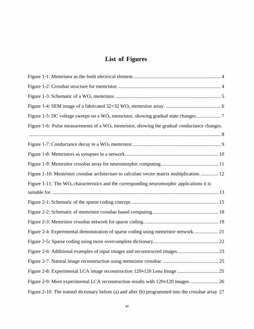
Figure 1-5: DC voltage sweeps on a WOx memristor, showing gradual state changes. The device conductance was increased during the 3 consecutive positive sweeps (red arrows), then
decreased during the 3 subsequent negative sweeps (blue arrows).
As with all memristor devices, a “pinched-hysteresis” behavior can be distinctively observed
in the I-V characteristics in the WOx memristor devices, as shown in Figure 1-5. When a positive
voltage is applied, the device conductance gradually increases (termed the write process) and when
a negative voltage is applied the conductance gradually decreases (termed the erase process).
Moreover, when multiple consecutive positive sweeps are applied, the device conductance
continues to increase with each sweep, but also exhibits overlaps between the hysteresis loops,
consistent with the short-term memory behavior discussed in refence17.
The gradual conductance changes can be more clearly observed by pulse measurements, as
shown in Figure 1-6. Here 50 write pulses (+1.4 V, 100 µs) were applied to the device, followed
by 50 erase pulses (-1.3 V, 100 µs). The device state was monitored by a small read pulse (0.5 V,
200 µs) after each write/erase pulse.

8868
0 100 200 300
0.6
0.8
1.0
1.2
1.4
1.6
Re
ad
Cu
rre
nt
(A
)
Pulse Number
Write
Erase
Figure 1-6: Pulse measurements of a WOx memristor, showing the gradual conductance changes. Positive write pulses (+1.4 V, 100 µs) gradually increase the device conductance (red squares) wile
negative erase pulses (-1.3V, 100 µs) gradually decrease the conductance (blue squares).
1.3.3 Device Modeling
The WOx device characteristics can be explained by the redistribution of ions, here in the
form of oxygen vacancies (Vos), as has been discussed in previous literatures12,19,20.
Specifically, the memristor dynamics can be described by the following equations:
𝐼 = (1 − 𝑤)𝛼[1 − 𝑒𝑥𝑝(−𝛽𝑉)] + 𝑤𝛾 sinh(𝛿𝑉) (1 − 1)
𝑑𝑤
𝑑𝑡= 𝜆𝑠𝑖𝑛ℎ(𝜂𝑉) −
𝑤
𝜏 (1 − 2)
Equation (1-1) is the I-V equation which includes a Schottky (the 1st term) corresponding to
conduction in the Vo-poor region and a tunneling-like term (the 2nd term) corresponding to the Vo-
rich region. The two conduction channels are in parallel and their relative weight is determined by
the internal state variable w.
Equation (1-2) is the dynamics equation which describes the change rate of the state variable
w with respect to the applied voltage, including the drift effect under an applied electric field (the
1st term) and the spontaneous diffusion (the 2nd term). 𝛼, 𝛽, 𝛾, 𝛿, 𝜆, 𝜂 are all positive-valued
parameters determined by material properties. 𝜏 is the diffusion time constant, which corresponds
to the retention or the decay speed of the memristor device.
During the device fabrication, we can tailor the oxidation conditions to achieve different

9868
device retention performance. With oxidation at a low temperature such as 375°C for 60s, we can
achieve the so-called short-term memory effect, which refers to the fact that the device can only
hold its conductance value for a short period of time (Figure 1-7). This type of memristor can be
used in certain applications that takes advantage of the short-term memory dynamics to process
temporal information, which will be discussed in Chapter 5. The time constant τ in the short-term
memory devices is typically around 50ms.
0 200 400 600 800
0.4
0.5
0.6
Rea
d C
urr
en
t (
A)
Time (ms)
After Write
Initial
Figure 1-7: Conductance decay in a WOx memristor.
The device was first programmed by 5 write pulses (1.4 V, 1 ms) then its conductance was monitored by periodic read pulses (0.4 V, 500 µs).
If we use stronger oxidation condition, e.g. 425°C for 60s, the device can obtain much longer
retention. In this case, we can use the memristor devices to store synaptic weights and to perform
matrix operation directly in the memristor arrays, as introduced in section 1.3.5. Examples of such
devices will be mentioned in Chapter 2 to Chapter 4.
1.3.4 Memristor as Synapse
With the ion-driven analog switching behavior, memristors can be used to naturally emulate
biological synapses. Synapses are connections between neurons, and provide critical functions to
transfer and regulate signals between neurons that form the basis of memory and cognition in
biological systems. There are ~1011 neurons and ~1014 synapses in a human brain7. Neurons and
synapses together make up neural networks, which are the building blocks that empower humans

10868
to learn, think and remember.
A key attribute of the brain’s computing power is that the synapses are “plastic” – that is,
the synaptic weight, or the connection strength between neurons, can be modulated and new weight
can be retained. Since the synaptic weight regulates the transmission of signals between neurons,
synaptic plasticity along with the very large synaptic connectivity empowers the efficient brain-
based parallel computing paradigm and lays the foundation of neuromorphic computing.
The prospect of building biologically inspired neuromorphic computing systems with
memristor networks21 has generated significant interest since memristors can phenomenologically
and bio-realistically emulate synaptic plasticity, and offer the desired large connectivity and low
power budget, as illustrated in Figure 1-821
Figure 1-8: Memristors as synapses in a network. Schematic illustration of the concept of using memristors as synapses between neurons. The insets
show the schematics of the two-terminal device geometry and the layered structure of the memristor. Image adapted from Reference [21]. Image credit: Dr. S.H. Jo
1.3.5 Memristor Crossbar Array for Neuromorphic Applications
A network of many memristor devices, formed in the structure of a crossbar array as shown
in Figure 1-9, can then be used to implement synaptic weights in general Artificial Neural Network
(ANN) applications. In particular, this type of crossbar array structure can perform many tasks that
are based on matrix operations efficiently, due to its ability to implement vector-matrix
multiplications in a natural and elegant fashion, using Ohm’s law and Kirchhoff’s current law.

11868
Figure 1-9: Memrsitor crossbar array for neuromorphic computing A memristor is formed at each crosspoint of the crossbar array. In this approach, vector-matrix
multiplication can be obtained through Ohm’s law and Kirchhoff’s law through a simple read operation. Image adapted from Reference [33]. Image credit: Dr. Mohammed A. Zidan
As illustrated in Figure 1-10, if an input vector x is fed to the crossbar with each element xi
applied on a row of the crossbar while keeping the columns grounded, the current flowing through
each memristor at the crosspoint (i, j) will be:
𝐼𝑖𝑗 = 𝑥𝑖𝑤𝑖𝑗 (1 − 3)
where xi represents the vector element which for example could be a pulse with a fixed
amplitude and width modulated according to the input, and wj represents the state of memristor,
i.e., the conductance (often called weight in neuromorphic systems). Since all memristors on one
column share the same bottom electrode, the current collected at column j is the sum of all the
currents flowing through the memristors on this column
𝐼𝑗 = ∑ 𝑥𝑖𝑤𝑖𝑗 = 𝐱 ⋅ 𝐖𝑗
𝑛
𝑖=1 (1 − 4)
Therefore, the current measured at column j represents the dot product of the input vector x and
the stored weight vector (often called the feature vector) 𝐖𝑗 in column j of the crossbar, 𝐱 ⋅ 𝐖𝑗 . By
collecting currents in all the columns, the vector-matrix multiplication (VMM) output, 𝐱 ⋅ 𝐖, can
then be obtained in a single “read” operation. This operation best represents the benefits of
computing in memristor crossbars – the ability to perform computing in the weight storage devices
directly, as well as the high-degree of parallelism where all devices in the crossbar operate in

12868
parallel and perform the multiply and add functions simultaneously.
Figure 1-10: Memristor crossbar architecture to calculate vector matrix multiplication. Inputs are applied on the rows as xi, while the current (charge) is collated on the columns, schematically
shown as Aj. Memristors are formed at the crosspoints with the weight wij.
Moreover, because the resistances of memristors can be readily modulated, neuromorphic
systems based on memristors can achieve online learning, by updating the resistances of the
memristors that form the feature vectors using voltage pulses with higher amplitudes that can drive
the internal ion migrations in the devices.
Due to the compact device structure and the ability to both store and process information at
the same physical locations, memristors and memristor crossbar arrays have been extensively
studied for neuromorphic computing and machine learning application such as single laye22,23 and
multi-layer perceptron networks24,25, image transformation26,27, sparse coding28, reservoir
computing29 and principal component analysis30. Our approach of implementing neuromorphic
applications will be discussed in detail in following chapters.
1.4 Organization of the Dissertation
In this chapter, we have introduced the memristor concept and the crossbar architecture. Our
studies are based on WOx memristor devices, where Figure 1-11 lists the main properties of the
device and the appropriate neuromorphic applications it is suitable for.
Specifically, for WOx devices with long retention, we can store analog information at large
scale. Combined with the crossbar configuration, it can be used to perform vector-matrix
multiplications. Furthermore, with the gradual analog switching behavior, online learning

13868
algorithms can be implemented in the memristor hardware system. On the other hand, for WOx
devices short-term memory, we can use their internal dynamics for temporal information
processing and reservoir computing applications.
Figure 1-11: The WOx characteristics and the corresponding neuromorphic applications it is suitable for.
The rest of the thesis will discuss a few studies based on the WOx memristor devices, and is
organized as following:
Chapter 2 discusses a sparse coding algorithm that has been implemented experimentally
with a WOx memristor crossbar network. Results of simple bar patterns and complex natural
images will be discussed.
Chapter 3 discusses the constraints in online dictionary learning with realistic memristor
devices and proposes a solution based on epsilon-greedy strategy to improve training performance.
Chapter 4 discusses a hybrid integrated system with the WOx arrays directly fabricated on a
custom-designed CMOS chip to implement multiple neuromorphic applications on-chip in a
functional, standalone system.
Chapter 5 discusses memristor-based reservoir computing, emphasizing the temporal
information processing ability of WOx memristors through its internal dynamics. Examples of digit
recognition and temporal signal processing will be presented.
Chapter 6 discusses two other possible neuromorphic applications for further research
directions.

14868
Chapter 2 Sparse Coding with Memristor Crossbar Array
From the discussion in Chapter 1, we learned that if constructed into the crossbar structure,
memristor networks can efficiently implement matrix operations, especially vector-matrix
multiplications (VMM) in parallel and with high energy efficiency. Neuromorphic computing
systems can be implemented in hardware based on this approach13,31–33, for tasks such as feature
extraction and pattern recognition22,23,27,30,34.
In this study, we experimentally demonstrate a sparse coding algorithm implemented in a
memristor crossbar network, and show that the memristor network can be used to perform
applications such as natural image processing with an offline learned dictionary set.
2.1 Sparse Coding
Sparse coding aims at representing the original data with the activity of a small set of
neurons, and can be traced to models of data representation in the visual cortex35,36. Sparse
representation reduces the complexity of the input signals and enables more efficient processing
and storage, as well as improved feature extraction and pattern recognition functions37,38.
The concept of sparse coding is as follows: Given an input signal, x, and a dictionary of
features, D, sparse coding aims to represent x as a linear combination of features from D using a
set of sparse coefficients a, with minimum number of features. Mathematically, the objective of
sparse coding can be summarized as minimizing an energy function containing both the
reconstruction error term as well as a sparsity penalty term, defined as:
min 𝑎
( |𝑥 − 𝐷𝑎𝑇|2 + 𝜆|𝑎|0 ) (2 − 1)
where |⋅|2 and |⋅|0 are the L2- and the L0-norm, respectively, and 𝜆 is a sparsity parameter
that determines the relative weights of the reconstruction error (1st term) and the sparsity penalty
(the number of neurons used, 2nd term).
A schematic of the sparse coding concept is shown in Figure 2-1, where an input (e.g. the

15868
image patch of a clock) is represented by a few features selected from a large dictionary35,38.
Figure 2-1: Schematic of the sparse coding concept.
An input (e.g., the image patch of a clock) can be decomposed into and represented with a minimal number of dictionary elements. The numbers in the images are just for illustration purpose and are not
the actual sparse code.
Sparse representation of information provides a powerful method to perform feature
extraction on high-dimensional data, and is of broad interest for applications in signal processing,
computer vision, object recognition and neurobiology37. Sparse coding is also believed to be a key
mechanism by which biological neural systems can efficiently process complex, large amount of
sensory data while consuming very little power36,38,39.
2.2 Locally Competitive Algorithm
The Locally Competitive Algorithm (LCA) is a sparse coding algorithm that uses a dictionary
of feature vectors (represented by synaptic weights) to transform a vector of input signal into a
relatively small number of output coefficients, which can be used for image compression or object
recognition40.
LCA solves the minimization problem in Equation (2-1) using a network of leaky-integrator
neurons and connection weights. Different from commonly used feed-forward neural networks,
LCA describes a dynamical system where neurons compete with each other in proportion to the
similarity of their respective receptive fields (the collection of synaptic weights entering a neuron).
In this approach, the membrane potential of an output neuron is determined by the input, a leakage
term, and an inhibition term whose strength is proportional to the similarity of the neurons’
features40 (an active neuron will try to inhibit neurons with similar features with itself). After the

16868
network get stabilized, an optimal sparse representation, out of many possible representations will
be obtained.
Mathematically, in LCA, x is an m-element column vector, with each element corresponding
to an input element (e.g. intensity of a pixel in an image patch). D is an m×n matrix, where each
column of D represents an m-element feature vector (i.e. a dictionary element) and connected to a
leaky-integrator output neuron. a is a sparse row vector of neuron activity coefficients, where the
ith element of a represents the activity of the ith neuron, whose feature vector is used in the data
reconstruction. After feeding input x to the network and allowing the network to stabilize through
lateral inhibition, a reconstruction of x can be obtained as 𝐷𝑎𝑇, and in a sparse representation only
a few elements in a are nonzero while the other neurons’ activities are suppressed to be precisely
zero40.
The neuron dynamics during LCA analysis can be summarized by Equation (2-2)
𝑑𝑢
𝑑𝑡=
1
𝜏(−𝑢 + 𝑥𝑇𝐷 − 𝑎(𝐷𝑇𝐷 − 𝐼𝑛)) (2 − 2𝑎)
𝑎 = 𝑢 if 𝑢 > 𝜆0 otherwise
(2 − 2𝑏)
where u is called neurons’ membrane potentials, τ is a time constant, and 𝐼𝑛 is the 𝑛 × 𝑛
identity matrix.
During LCA analysis, each neuron i integrates its input 𝑥𝑇𝐷, leakage −𝑢, and inhibition
𝑎(𝐷𝑇𝐷 − 𝐼𝑛) terms and updates its membrane potential 𝑢𝑖 in Equation (2-2a). If and only if 𝑢𝑖
reaches above a threshold (set by parameter λ), neuron i will produce an output 𝑎𝑖 = 𝑢𝑖, otherwise
the neuron’s activity 𝑎𝑖 is kept at 0 (as in Equation (2-2b)).
Specifically, the input to neuron i results from the signal x scaled by the weights 𝐷𝑗𝑖
connected to the neuron (second term in Equation (2-2a)). To this regard, the collection of the
synaptic weights 𝐷𝑗𝑖 associated with neuron i, corresponding to a feature column of D, is also
referred to as the receptive field of neuron i, analogous to the receptive fields of biological neurons
in the visual cortex38,41. A key feature of LCA is that the neurons also receive inhibition from other
active neurons (last term in Equation (2-2a)), an important feature in biological neural systems38.
LCA incorporates this competitive effect with the inhibition term proportional to the similarity of
the neurons’ receptive fields40 (measured by 𝐷𝑇𝐷 in Equation (2-2a)). By doing so, it prevents
multiple neurons from representing the same feature and allows the network to dynamically evolve

17868
to find an optimal output. Note that when a neuron becomes active, all other neurons’ membrane
potentials will be updated through the inhibition term (to different degrees depending how similar
the neurons’ receptive fields are). As a result, an initially active neuron may become suppressed
and a more optimal representation that better matches the input may be found. In the end the
network evolves to a steady state where the energy function (Equation (2-1)) is minimized and an
optimized sparse representation (out of many possible solutions) of the input data is obtained from
a combination of stored features based on the active neurons.
Note however implementing the inhibition effect 𝐷𝑇𝐷 can be computationally intensive. On
the other hand, the original Equation (2-2a) can be re-written into Equation (2-3) below
𝑑𝑢
𝑑𝑡=
1
𝜏(−𝑢 + (𝑥 − )𝑇𝐷 + 𝑎) (2 − 3)
where = 𝐷𝑎𝑇 is the signal estimation (i.e. the reconstructed signal). Equation (2-3) shows
that the inhibition term between neurons can be reinterpreted as a neuron removing its feature from
the input when it becomes active, thus suppressing the activity of other neurons with similar
features. By doing so, the matrix-matrix operation 𝐷𝑇𝐷 in Equation (2-2a) is reduced to two
sequential matrix-vector dot-product operations (one used to calculate = 𝐷𝑎𝑇 and the other
used to calculate the contribution from the updated input (𝑥 − )𝑇𝐷), which we show can be
efficiently implemented in memristor crossbars in discrete time domain without physical inhibitory
synaptic connections between the neurons.
2.3 Mapping Sparse Coding onto Memristor Network
As discussed in Chapter 1, memristor crossbars are particularly suitable for implementing
neuromorphic algorithms, because the vector-matrix multiplication operations can be performed
through a single read operation in the memristor array32,42.
We experimentally implemented the sparse coding algorithm in the memristor array-based
artificial neural network, schematically shown in Figure 2-2. In this implementation, x is an m-
element column vector applied to the rows of the memristor crossbar (cyan pads on the left), with
each element corresponding to an input element (e.g. intensity of a grayscale pixel in an image
patch). It is implemented by read pulses with a fixed amplitude but variable width proportional to
the pixel intensity.
18868
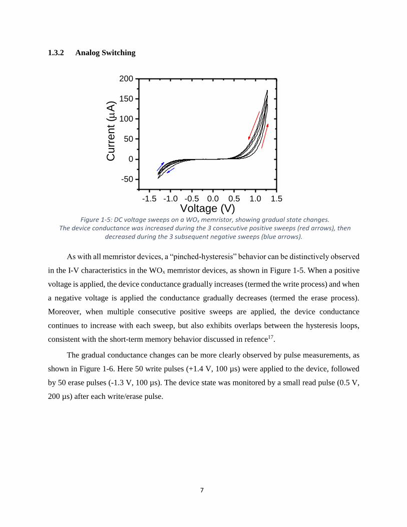
Figure 2-2: Schematic of memristor crossbar based computing. A memristor is formed at each crosspoint and can be programmed to different conductance states
(represented as grayscale color).
In this approach, the dictionary, D, is directly mapped element-wise into the memristor
crossbar with each memristor at row i and column j storing the corresponding synaptic weight
element Dij. The input vector x (e.g. grayscale pixel intensities of the input image when used in
image analysis) is implemented with read pulses with a fixed amplitude and variable width
proportional to the pixel intensity. As a result, the total charge Qij passed by a memristor at
crosspoint (i,j) is linearly proportional to the product of the pixel intensity xi and the conductance
Dij of the memristor 𝑄𝑖𝑗 = 𝑥𝑖𝐷𝑖𝑗 , and the charge passed by all memristors sharing column j is
summed via Ohm’s Law and Kirchhoff’s current law: 𝑄𝑗 = ∑ 𝑥𝑖𝐷𝑖𝑗𝑖 = 𝑥𝑇𝐷𝑗 (Figure 2-2). In other
words, the total charge accumulated at neuron j is proportional to the dot-product of the input x
with the neuron’s receptive field Dj.
Since the dot-product of vectors measures how close the input vector is matched with the
stored vector, the ability to implement this operation in a single read process allows the memristor
network to conveniently and efficiently perform this important pattern matching task. This term
(𝑥𝑇𝐷 in vector form) is then added to the neuron’s membrane potential following Equation (2-3),
a leakage term is subtracted, and the membrane potential is then compared to the threshold
parameter, λ. If the membrane potential is above threshold , the neuron is active for the next
phase.
In the second phase, the input image is reconstructed using the currently active neurons and
compared to the original input. This is accomplished by performing a “backward read”: variable

19868
width read pulses, proportional to the neurons’ activities 𝑎𝑗, are applied on the columns while the
charge is collected on each row i to obtain 𝑄𝑖 = ∑ 𝐷𝑖𝑗𝑎𝑗𝑗 = 𝐷𝑖𝑎𝑇. This backward read has the
effect of performing a weighted sum of the receptive fields of the active neurons, and the total
integrated charge on the rows is proportional to the intermediate reconstructed signal = 𝐷𝑎𝑇 in
vector form. The difference of x and , referred to as the residual, is used as the new input to the
array to obtain an updated membrane potential. The forward and backward processes are repeated,
alternately updating the neuron activities and then the residual. The updated value is calculated
from Equation (2-2) and (2-3) by a FPGA board in the measurement setup. After the network has
stabilized, a sparse representation of the input, represented by the final output activity vector a, is
obtained. By performing these forward and backward passes in the same memristor network in
discrete time domain, we can effectively achieve lateral inhibition required by the sparse coding
algorithm, without having to implement physical inhibitory synaptic connections between neurons.
Figure 2-3: Memristor crossbar network for sparse coding. Upper right inset shows a magnified scanning electron microscope (SEM) image of the crossbar. Lower
left inset shows the memristor chip integrated on the testing board after wire-bonding.
In this study, the hardware system used is a 32×32 memristor crossbar array, where a
memristor formed at each intersection in the crossbar (Figure 2-3). The WOx memristor devices
are fabricated by Dr. Chao Du following the previously developed proocess18 discussed in Chapter
1. When fabrication is completed, the memristor crossbar array chip is wire-bonded and integrated
on a custom-designed testing printed circuit board (PCB), as shown in the lower inset of Figure
2-3. Dr. Patrick M. Sheridan and Zelin Zhang also helped tremendously in building the hardware and

20868
software of testing platform.
During experimental measurements, the original input (for example an image) is fed to the
rows (which are the top electrodes) of the memristor array and the columns (which are the bottom
electrodes) of the array are connected to output neurons. The memristor network performs critical
pattern matching and neuron inhibition operations to obtain a sparse, optimal representation of the
input. After the stabilization of the memristor network, the re-constructed image can be obtained
based on the (sparse) output neuron activities and the features stored in the crossbar array.
2.4 Sparse Coding Results of Simple Inputs
To experimentally demonstrate sparse coding with the memristor network, we start with
simple inputs such as grayscale horizontal and diagonal bar patterns for image reconstruction.
The first demonstration is encoding an image composed of diagonally oriented stripe features
using the algorithm given above. The dictionary, shown in Figure 2-4a, contains 20 features with
each feature consisting of 25 weights. The 20 features were written into the 20 columns (with each
weight represented as a memristor conductance) and the inputs were fed into the 25 rows, which
means a 25×20 sub-array was used out the 32×32 memristor array in this experiment. An input
signal, shown in Figure 2-4b and consisting of a combination of 4 features, is used as a test input
to the system.
The network stabilizes after 30 forward-backward iterations, and the final signal
reconstruction is shown in Figure 2-4b. It can be seen that the input image can be correctly
reconstructed with neurons 2, 6, 9, and 17, corresponding to the features of the input, weighted by
their activities. Additionally, the experimental setup allows us to study the network dynamics
during the analysis.
21868
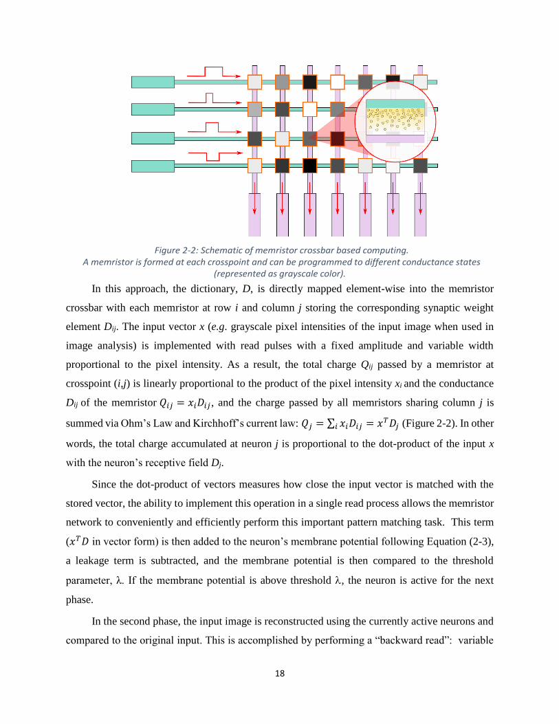
Figure 2-4: Experimental demonstration of sparse coding using memristor network. a) Dictionary elements programmed into the memristor crossbar array, each dictionary element is
stored in a single column. b) The original and the reconstructed image after the memristor network settles. c) Membrane potentials of the neurons as a function of iteration number during LCA analysis. Red horizontal line: threshold parameter. d) Additional examples of input images and reconstructed
images.
Figure 2-4c plots the membrane potential values for all 20 neurons during the iterations. It
can be seen that for the first 2 iterations, all neurons are charging (at somewhat different rates
depending on how well the input is matched with the stored receptive fields, which is in turn
affected by device variabilities) and none are above threshold. After the 4th iteration, the membrane
potentials of 11 neurons (numbers 1, 2, 4, 5, 6, 9, 10, 13, 14, 16, 17) have exceeded the threshold.
Out of these 11 neurons, the receptive fields of neurons 2, 6, 9, and 17 match the features in the
input, while those of neurons 1, 4, 5, 10, 13, 14, 16 are not perfect matches but still overlap enough
with the input image to allow these neurons to be charged at reasonable rates. In the subsequent
backward read, all the active neurons will contribute their receptive fields to the reconstruction,
and result in a reduced residual input. As a result, there is a reduction in the charging rates and a
decrease of the neurons’ membrane potentials at iteration 5 due to the leaky term in Equation (2-
3). Over the next a few iterations the lateral inhibition between neurons eventually drives the
membrane potentials of neurons 1, 4, 5, 10, 13, 14, 16 below the threshold in the 10th iteration and
keep these neurons inactive in subsequent iterations. The inactive neurons’ membrane potentials

22868
continue to decay due to the leakage term, but because they are below threshold, their values have
no impact on the final sparse code. In the end, a correct and sparse representation of the input is
reconstructed in Figure 2-4b based on the active neurons 2, 6, 9, and 17 after the network stabilizes.
This experiment demonstrates an important feature of the sparse coding algorithm: lateral
inhibition mechanisms drive the system to accurately represent the input. Non-idealities in the
memristor network may temporarily lead to incorrect behavior (as in the case of the 4th iteration
or the 8th iteration when neurons 4, 14, 16 exceed the threshold), but the lateral inhibition inherent
in the neuron dynamics can effectively correct these errors. These features of the network
dynamics have been further analyzed through simulations of the memristor crossbar-based sparse
coding hardware. Additional examples of inputs composed of two features and the reconstructed
images from the memristor crossbar can be found in Figure 2-4d.
Figure 2-5: Sparse coding using more overcomplete dictionary. a) Dictionary elements based on horizontal and vertical bars programmed into the memristor
crossbar array. b) The original image to be encoded and the reconstructed image after the memristor network settles. c) Membrane potentials of the neurons as a function of iteration
number during LCA analysis. Red horizontal line: threshold parameter.
The re-programmability of memristors allows the dictionary set to be readily adapted to the
types of signals to be encoded, so the same memristor hardware system can process different types
of inputs using a single general approach. To demonstrate this point, we re-programmed a new
dictionary composed of horizontally and vertically oriented bars (Figure 2-5a) into the same array
used in studies in Figure 2-4. By using this new dictionary, images consisting of bar patterns can
be efficiently reconstructed using the same algorithm. More importantly, in order to demonstrate
the capability of sparse coding to find the optimal solution out of several possible solutions, a
dictionary that is larger than the input space, e.g. a so-called over-complete dictionary set40, is used

23868
in the examples shown in Figure 2-5a, the dictionary is minimally over-complete (since the input
is restricted to be the combinations of the diagonal stripe features and corresponds to an input
dimensionality of 17, determined from the linear span of the features). By using the bar patterns
in Figure 2-5a and restricting the input images to only combinations of horizontal and vertical bars,
the input dimensionality is reduced to 9. With a total of 20 stored dictionary elements, the system
now achieves greater than 2× over-completeness in such a relatively small network and should be
better to highlight the effects of sparse coding.
The resulting reconstructions using this overcomplete dictionary are shown in Figure 2-5b
and Figure 2-5c. The network not only correctly reconstructed the input image, but as expected, it
picked the more efficient solution – a solution based on neurons 8 and 16, over another solution
based on neurons 1, 4, and 8. As can be seen from Figure 2-5c in the first 5 iterations, all neurons
are charging and the membrane potentials of neurons 1, 4, 8 and 16 first cross the threshold at
iteration 6. Even though the receptive fields of all the four neurons (1, 4, 8 and 16) are correct
features in the input, neurons 8 and 16 (consisting of two bars) represent a sparser representation.
As a result, inhibition implemented in the system eventually suppresses the membrane potentials
of neurons 1 and 4 to be below the threshold after iteration 11 and keeps them below the threshold
after the network stabilizes. As a result, the activities of these two neurons are set to be precisely
0 (Equation (2-2b)), and an optimal solution based only on neurons 8 and 16 is obtained, compared
to other possible, less-sparse solutions.
Figure 2-6: Additional examples of input images and reconstructed images. The same threshold 𝜆 = 40 is used in all experiments.

24868
To further demonstrate the performance of the robustness of the hardware system, an
exhaustive test of all 50 patterns consisting of two horizontal bars and one vertical bar were
performed (Figure 2-6) with a success rate of 94% (measured by the network’s ability to correctly
identify the sparse solutions), despite variabilities inherent in the memristor devices.
2.5 Sparse Coding Results of Natural Images
Other than simple inputs like bar patterns, we have also demonstrated that our memristor
network can perform sparse coding for more complex and interesting input patterns, such as
grayscale natural images, using the sparse coding algorithm and a learned dictionary.
In this study, a 16×32 subarray was used out of the 32×32 memristor array, corresponding
to a 2× overcomplete dictionary with 16 inputs and 32 output neurons and dictionary elements.
The dictionary elements were learned offline using 4×4 patches randomly sampled from a training
set consisting of nine natural images (with sizes of 128×128 pixels), using a realistic memristor
model and an algorithm based on the winner-take-all (WTA) approach and Oja’s learning rule43.
More details on the training process can be found in Chapter 3.
After training, the obtained dictionary elements were programmed into the physical 16×32
crossbar array (more details will be discussed in Section 2.6). Using the trained dictionary, we
successfully performed reconstruction of 120×120 pixel grayscale images experimentally using
the 16×32 memristor crossbar. During the process, the 120×120 input image (Figure 2-7a) was
divided into 4×4 patches and each patch was experimentally processed using the memristor
crossbar and the Locally Competitive Algorithm (Figure 2-7b). After the memristor network
stabilized (typically after 80 forward/backward iterations (Figure 2-7d), the patch was
reconstructed using the neuron activities and the corresponding receptive fields stored in the
crossbar array, as shown in Figure 2-7c.

25868
Figure 2-7: Natural image reconstruction using memristor crossbar. a) Original 120×120 image, which is divided into 4x4 patches. b) A 4×4 patch from the original image. c)
The experimentally reconstructed patch with memrsitor network. d) Membrane potentials of the neurons as a function of iteration number during LCA analysis. Red horizontal line: threshold parameter.
The complete image was then composed from the individual patches, shown in Figure 2-8.
The reconstructed successfully captured the main features of the original Lena image.
Figure 2-8: Experimental LCA image reconstruction 120×120 Lena Image

26868
To further demonstrate the functionality of the hardware sparse coding system, we tested
five other commonly studied images, with different color tones (e.g. with a black or white
background) and different features, shown in Figure 2-9. As can be seen from the results, the
memristor-based sparse coding system can perform satisfactory reconstruction for all cases,
regardless of the content of the figures.
Figure 2-9: More experimental LCA reconstruction results with 120×120 images.
2.6 Nonideality Effect on Image Reconstruction with Sparse Coding
We note the reconstructed images in Figure 2-8 and Figure 2-9 were still not perfect, both
experimentally and in the simulation. The imperfect image reconstruction can be caused by serval
reasons:
First, due to the device to device variations, the dictionary programmed into the memristor
array is not exactly the same as the ideal dictionary obtained from training, and only maintains the
major features of the original dictionary elements.
Moreover, due to the limited dictionary size, the small basis space limits the types of features
in the trained dictionary to be mainly low-spatial frequency features. The system thus cannot
reconstruct the high-spatial frequency features effectively, which leads to lack of fine-grained
details in the final image.
Another reason lies in the limitation of the learning algorithm itself, which will be discussed
in detail in Chapter 3. In this section, we will focus on the first two issues.

27868
2.6.1 Effect of Device-to-Device Variations
During the natural image reconstruction with offline learned dictionary, the obtained
dictionary elements need to be programmed into the physical 16×32 crossbar array. However,
since the memristor crossbar array has intrinsic device-to-device variations, the stored dictionary
will not be exactly the same as the ideal leaned dictionary. The effect of the device variations on
the experimentally stored dictionary is shown in Figure 2-10.
Figure 2-10: The trained dictionary before (a) and after (b) programmed into the crossbar array
With the intrinsic device variations, the dictionary after programmed is slightly distorted from the ideal version.
Figure 2-10b shows the dictionary elements experimentally stored in and read out from the
memristor crossbar and used for the experimental natural image reconstructions. Due to intrinsic
device variations, the patterns stored in the array (Figure 2-10b) are slightly distorted from ideal
dictionary (Figure 2-10a), but generally maintain the main features of the learned dictionary
elements. Here the dictionary set was written into the array using a single shot method, without
repeated read verification and re-programming steps.
This nonideal stored dictionary is one of the reasons of the imperfect image reconstruction.
To verify the validity of our experimental approach, we performed a realistic simulation using a

28868
device model that incorporates device variations during the weight changes, so that we can repeat
effect of the nonideal device variation on the image reconstruction.
To model the device variations during weight updates, we experimentally measured the
incremental conductance changes in 288 devices in the memristor array using pulsed
programming/erasing conditions. The results are shown in Figure 2-11. Here each device was
programmed with 20 write pulses and followed by 20 erase pulses, and the device conductance
was monitored after each write/erase pulse by a read pulse.
We fitted the experimental data with the memristor model we discussed in Chapter 1
𝐼 = 𝑤(𝛾 sinh(𝛿𝑉)) + (1 − 𝑤) (𝛼(1 − 𝑒−𝛽𝑉)) (2 − 4𝑎)
𝑑𝑤
𝑑𝑡= 𝜂1 sinh(𝜂2𝑉) 𝐹(𝑤, 𝑉) (2 − 4𝑏)
where Equation (2-4a) is the current-voltage equation dependent on the internal state variable
w, and Equation (2-4b) describes the update rate of the state variable. Since we the device in the
sparse coding applications have long retention performance, we can ignore the 𝜏 term in Equation
(2-4b).
F(w,V) is a window function, which is used to fit the asymmetricity in write and erase:
𝐹(𝑤, 𝑉) = 1 − 𝑤, 𝑖𝑓 𝑉 > 0 𝑤, 𝑖𝑓 𝑉 < 0
(2 − 5)
In our device model we assumed that the initial values of the state variable (w0) from
different devices follow the same Gaussian distribution as observed in Figure 2-11b. During
weight updates, we further assumed that the parameters 𝜂1 and 𝜂2 in the weight update equation
(Equation (2-4b)) are different for different devices, also following Gaussian distributions. With
these modifications to the original ideal device model, the experimentally observed variations
during weight updates can be realistically accounted for, as shown in Figure 2-11c, for the same
programming/erasing conditions used in the experiments. Exact parameters used in the model are
shown in Table 2-1.

29868
Figure 2-11: Experimental pulse write and erase curves from 288 memristor devices (a) Pulse write/erase data measured from 288 devices in the memristor array. (b) Initial
conductance distributions. (c) Simulation fitted 288 memristor devices using device model with device-to-device variations (d) Simulation fitted initial conductance distribution
𝑝(𝑤𝑜 = 𝑤) = 1
√2𝜎2𝜋𝑒
−(𝑤−𝜇)2
2𝜎2
µ 0.03 𝛼 10-8
𝜎 0.009 𝛽 0.5
𝛾 10-5 𝜂1 9×10⁻⁸ with 3% variation
𝛿 4 𝜂2 15.5 with 1% variation
Table 2-1: Experimentally extracted parameters used in the device model simulation.
Non-idealities during the dictionary storage were simulated based on the weight update
equation from our device model, after considering device variation effects. It can be observed in

30868
Figure 2-12 that our device model can successfully captured the device-to-device variation effect
on the dictionary programming.
Figure 2-12: Verification of the device variation on dictionary programming (A) Experimentally stored dictionary elements in the memristor crossbar. (B) Simulated stored weights
after considering device variations.
Furthermore, in Figure 2-13, simulations of image reconstruction were then performed using
the simulated stored dictionary elements, following the same procedure as the experimental
processes. The simulation results consistently reproduced the experimental results (Figure 2-13b)
for this image processing task.
(A) (B)

31868
Figure 2-13: Verification of the device variation effect on image reconstruction
a) Experimentally reconstructed image based on the reconstructed patches. b) Simulated reconstructed image using offline trained dictionary based on WTA.
2.6.2 Effect of Limited Dictionary Size
Another limitation of the current experimental sparse coding setup is the limited dictionary
size. Although the dictionary is 2× over-complete, there are still only 32 features in total in the
dictionary. As a result, the performance of the reconstruction of natural images, which are
generally complex and include both low- and high-spatial frequency features, will not be perfect
with these small dictionaries limited by the current experimental setup.
Despite the limits of the small dictionary size, during the process of each 4×4 patch the
system was still able to perform reconstruction following the LCA algorithm based on the features
in the dictionary, as shown in Figure 2-7. To have a closer look at the details of the image
reconstruction results, we show below several additional zoomed-in areas of the original Lena
image (Figure 2-14) compared with experimental and simulation reconstruction results (Figure
2-15).

32868
Figure 2-14: Selected regions in the Lena image used for comparison.
As can be seen from Figure 2-15, the experimental reconstruction based on the memristor
array can clearly capture key features of the original image, albeit with a lower resolution due to
the lack of high-spatial frequency features in the dictionary as discussed earlier. For instance, we
can clearly observe the shape of the eyeballs in example Figure 2-15(a), where distinct differences
between patch to patch can be seen. Other examples Figure 2-15(b-e) also demonstrate the
experimental system’s ability to capture continuous edges and shades within and across multiple
patches, without overlapping the patches during reconstruction.

33868
Figure 2-15: Comparison of the highlighted regions showing the original, experimental and simulated reconstruction results.
Original Experimental Simulation
(a)
(b)
(c)
(d)
(e)

34868
Figure 2-16: Effect of improvement by using larger dictionary (a) Simulated reconstructed images with different dictionary sizes. (b) Results from the zoomed-in eye
region (marked in the original image in (a)), showing fine features can be captured with increased dictionary size.
To further verify that the apparent limited resolution of the reconstruction is due to the
limited dictionary size in this prototype system, we performed extended simulation studies to
analyze the effect of the dictionary size on the reconstruction results. As can be seen in Figure
2-16, with the increase of the dictionary size, from 32 features to 64, 96, 128 and 160 features
while keeping the input size and all other parameters fixed, the quality of the reconstruction
improves. This effect is also more clearly illustrated by showing results in the marked region
(Figure 2-16b). The fine features can now be captured by simply increasing the dictionary size
(a)
Original Image Reconstructed with 32 Elements Reconstructed with 64 Elements
Reconstructed with 96 Elements Reconstructed with 128 Elements Reconstructed with 160 Elements
(b)
32 elements 64 elements 96 elements 128 elements 160 elements

35868
while keeping all parameters fixed. These analyses verify the potential of using memristor
networks to perform image analysis tasks, if the network size can be increased to a more practical
size (e.g. from 16×32 used in the prototype system to larger sizes such as 16×160 in the future).
2.7 Benchmarking of Sparse Coding for Video Processing
Many real-world applications such as video processing are well suited for sparse coding. We
carried out analysis on how the memristor-based hardware will perform in video processing tasks.
Figure 2-17 shows an example of a 256×192 grayscale image, which was down-sampled from an
original 640×480 image. The image was then processed by the 16×32 memristor crossbar using
4×4 patches. During the process, 3072 (64×48) 4×4 patches were processed using the LCA
algorithm and each patch took 300 iterations to allow the network to stabilize. Due to the limited
data transfer rate between the memristor array and the digital circuitry in the existing test board,
the current memristor board will not be able to perform this video analysis in real time. However,
in an integrated memristor/CMOS system with a minimum possible read pulse width of 10 ns, our
analysis shows that it will take 0.034 second to process such an image, meeting the requirement
of real-time streaming video analysis at a rate of 24 frames/s (<0.042 second process time per
frame).
Figure 2-17: 256×192 video frame reconstructed using 4×4 patches using the 16×32 memristor crossbar.
To process standard 480p (640×480) videos with at least 24 frames/second frame rate
without down-sampling, larger patches (e.g. 10×10) will be needed. A memristor array size of
100×200 will be able to process the 480p videos in real time using 10×10 patches. Figure 2-18
shows simulation results of image reconstruction using the larger memristor array.

36868
Figure 2-18: 640×480 video frame reconstructed using 10×10 patches with a 100×200 memristor crossbar.
We then compared the performance of the memristor system with efficient digital solutions.
For a fair comparison of the crossbar-based analog solution with a digital solution, both methods
need to be subjected to the same constraints, as tradeoffs can always be made between low energy
consumption, fast speed and high reconstruction accuracy. In this application, we are targeting
power and processing time as the main performance metrics for both systems.
To achieve the benchmarking results, we designed and analyzed an efficient digital system
using efficient multiply-accumulation (MAC) circuits. Since an a×b crossbar can perform the (1×a)
× (a×b) vector-matrix dot-product operation in one read process in the memristor system, the
digital CMOS system was designed to match the same performance. Specifically, for
benchmarking purpose we assumed that in an integrated memristor chip a read speed of 10 ns can
be achieved. To obtain similar performance in the digital system, we used 4-bit × 4-bit
multiplications to approximately match the dynamic range of the input and the stored values in the
memristor crossbar. In the analysis, we used 10×10 patches (aimed for real time processing of
480p video) to sample and reconstruct the image. A 100×200 memristor crossbar was assumed for
the memristor implementation. The equivalent digital system in 40 nm CMOS uses 1600 MAC
circuits (8 MAC circuits per column and 200 columns operated in parallel) to accomplish one
(1×100) × (100×200) vector-matrix dot-product operation in 10.4 ns. Schematic and parameters
of the digital system are shown in Figure 2-19 and Table 2-2: Equivalent digital CMOS design of
a 100×200 crossbar using 40nm CMOS Technology, respectively. This design occupies 0.306
mm2 and it is estimated to consume 274 mW during the forward pass (reconstruction phase) stage
and 548mW during the backward pass (residual calculation) stage.

37868
Figure 2-19: Architecture of the digital CMOS system with 1,600 4b×4b multipliers, 8 per column; 1,600 adders, 8 per column; and 8 multiplication and
accumulation (MAC) per clock cycle per column. Each MAC operation is pipelined to 3 stages. Latency: 16 clock cycles to complete one (1×100) × (100×200) vector-matrix dot-product operation.
(1×100) × (100×200)
operation
Number of Multiply-accumulate (MAC) 1600
Number of pipeline stages 3
Clock period (ns) 0.65
Latency (ns) 10.4
Power consumption (mW) 274
Silicon area (mm2) 0.306
Power efficiency (TOPS/W) 7.02
Area efficiency (TOPS/mm2) 6.28 Table 2-2: Equivalent digital CMOS design of a 100×200 crossbar using 40nm CMOS Technology
The comparison between the memristor solution and the digital solution is shown below in
Figure 2-20 and Table 2-3: Performance comparison between the memristor solution and the
digital solution. The test is based on reconstructing 640×480 natural images at a rate of >24
images/second (e.g. real time processing of 480p videos).

38868
Figure 2-20: Image reconstruction results based on a memristor system and an efficient digital approach.
MSE L0 Time energy
Memristor 1.933×10⁻³ 15.6% 0.03607s 719.0µJ
Digital 2.226×10⁻³ 11.3% 0.02636s 11.82mJ
Table 2-3: Performance comparison between the memristor solution and the digital solution
As can be observed from the simulation results, the speed, error and sparsity parameters are
similar for the digital solution and the memristor solution, by design. The digital solution resulted
higher mean square error but lower L0. These can be explained by the quantization effect of the
digital approach. In the digital implementation, the synaptic weights were quantized into 4 bits (16
levels), which leads to a quantization error and subsequently slightly higher reconstruction error.
When it comes to power consumption, on the other hand, the memristor analog solution,
based on parameters used in the current prototype devices, already demonstrates significant (~16×)
improvement over the already very efficient digital solution. This is due to the fact that the vector-
matrix multiplication is obtained in a single step by a parallel read process in the memristor system.
To achieve the similar throughput in the digital system, eight 4b×4b multipliers were needed in a
single column, leading to higher energy consumption. We expect the advantage of the memristor
system will be even more pronounced for more complex tasks and with further optimized devices,
since in the digital solution analysis we neglected the time and energy costs associated with moving
data between the memory (not considered in this simple analysis) and the MAC circuitry, which
will not be negligible for larger input data, while in the memristor system such data movement is
not needed since the computation is directly performed in the same physical locations as the stored
weights. The energy cost in the memristor system can also be significantly lowered further by
Original Image Memristor solution Digital solution

39868
optimizing the memristor devices, i.e. by using lower current memristor devices.
2.8 Conclusion
Utilizing the merits of memristor crossbar network, i.e., natural implementation of vector-
matrix multiplication and weight storage/modulation, an important neuromorphic algorithm, LCA,
is demonstrated experimentally on a fabricated WOx memristor crossbar array. The algorithm can
be used to code and reconstruct patterns and images under desired sparsity constraints.
Beyond encoding bar patterns, we demonstrated that the memristor array can be used to
experimentally code and reconstruct natural images. The dictionary elements were obtained offline
using a realistic memristor model and an approach based on winner-take-all (WTA) and Oja’s
learning rule. The obtained dictionary elements were programmed into a physical 16×32 crossbar
array. Using the trained dictionary, we successfully preformed reconstruction of 120×120 pixel
grayscale images using the 16×32 memristor crossbar array.
Furthermore, with a benchmark of video processing simulation, we have demonstrated that
with comparable image processing throughput, the memristor sparse coding system can achieve
around 16× energy efficiency than a classic CMOS digital implementation using the current
devices, with higher efficiency expected with future device and architecture optimizations.

40868
Chapter 3 Online Dictionary Learning with Nonideal Memristor
Network
The Locally Competitive Algorithm (LCA), as described in Chapter 2, is mainly focused on
inference, which is to represent an input with a given dictionary. The dictionary used in LCA
implementation is learned offline in software. However, since the conductance state of memristor
devices can be dynamically fine-tuned, memrsitor crossbar arrays have the potential to perform
online learning in hardware, including feature vector learning for feedforward networks (which
will be further discussed in Chapter 4) as well as dictionary learning for sparse coding.
A conventional approach for online dictionary learning is to learn through sparse coding,
with the learning rule of stochastic gradient descent (SDG). It usually requires some image
preprocessing, say whitening and mean removal, to improve training efficiency, which increases
the complexity of hardware implementation. Even without image preprocessing, dictionary
learning through sparse coding can be time consuming and computationally expensive and is not
a very hardware-friendly approach taking into consideration the model complexity and device
limitations. These limitations lead us to explore a more suitable algorithm.
Instead, in our experimental LCA implementation we proposed an alternative learning
algorithm based on Oja’s learning rule in conjunction with winner-take-all (WTA), which enabled
fast training of the network to achieve excellent reconstruction performance43. However, when
considering experimental constraint of relatively large learning rate and lack of normalization, the
dictionary elements can be unevenly trained, leading to badly-learned dictionary.
In this section, we discuss our approach to learn the dictionary of feature primitives using
memristor crossbar array, in the presence of device nonideality and realistic experimental
constraints. Specifically, an epsilon-greedy strategy is applied to winner-take-all algorithm to
avoid uneven training through dictionary elements due to large device to device variations.
Ideally, one would also like to perform online learning experimentally using the same
memristor crossbar system. However, the slow speed of the board combined with the large training

41868
set prevented us from experimentally implementing online learning in the memristor crossbar. To
test the feasibility of online learning we instead performed a detailed, realistic simulation using a
device model that incorporates device variations during the incremental weight updates (see
Section 2.6.1).
3.1 Dictionary Learning through Sparse Coding
Online dictionary learning can be achieved by using sparse coding algorithm combined with
gradient descent, in which sufficient number of training patches are fed into the network and sparse
coefficients are obtained by using the sparse coding algorithm, followed by weight updates to
reduce the reconstruction error. Stochastic gradient descent is often used instead of batch gradient
descent to speed up the learning approach due to the large number of training samples used in the
process.
In our SDG implementation, we first initialized the memristor dictionary to random values,
and then for each training sample, we obtained the residual error (𝑥 − 𝐷𝑇𝑎) following the sparse
coding algorithm (which in our case is LCA), and updated the memristor weights directly by
increasing or decreasing their values according to the stochastic gradient descent rule, which is
described as:
ΔΦT = 𝛽(𝑥 − 𝐷𝑇𝑎)⨂𝑎 (3 − 1)
where 𝐷 is the matrix of dictionary elements (receptive fields), ⨂ is the outer product, 𝑥 −
𝐷𝑇𝑎 represents the reconstruction error with 𝐷𝑇𝑎 being the reconstructed input based on LCA,
and 𝛽 is the learning rate factor. Note that the dimension of (𝑥 − 𝐷𝑇𝑎)⨂𝑎 is the same as the
weight matrix.
This learning approach usually includes a mechanism to control and rescale the ℓ2-norm of
the dictionary elements. Without such a mechanism, the norm of D would arbitrarily go to infinity,
leading to small values for the coefficients ai44
.
In Chapter 2, the dictionary is trained offline in software and then programmed into the
physical array. To train the network, 4×4 patches are randomly sampled from a training set of nine
natural images (128×128 pixels) as the training input, shown in Figure 3-1.

42868
Figure 3-1: Training set used to obtain the dictionary
3.1.1 Dictionary Learning with Whitening
Some preprocessing methods are usually taken before online dictionary learning, such as
whitening and mean removal, to improve the learning efficiency in many algorithms. As discussed
in Olshausen & Field35, high spatial features in the dictionary may be more effectively trained
using a whitening technique that filters out the low spatial frequency components. Specifically, a
combined whitening/low-pass filter with a frequency response shown in Equation (3-2) has been
shown to lead to desired performance:
𝑅(𝑓) = 𝑓𝑒−(
𝑓𝑓0
)𝑛
(3 − 2)
The same combined whitening/low-pass filter was used to pre-process the image patches
before training, where 𝑓0 was chosen to be 200 cycles/picture and n was set to be 4.
The training data were sampled from ten 512×512 natural images with 12×12 patches.
Before the training, all patches were pre-processed using the combined whitening/low-pass filter
shown in Equation (3-2). Figure 3-2 shows the original image before and after whitening, as well
as the profile of the combined whitening/low-pass filter in frequency domain.

43868
Figure 3-2: The original image before and after whitening
along with the profile of the whitening/low-pass filter plotted in frequency domain.
12×12 whitened image patches, randomly sampled from the image set, were used as input
patches for dictionary training, following previous mentioned gradient descent training algorithm.
Figure 3-3 shows the 576 dictionary elements after training (using 12×12 image patches and
a 4× overcomplete dictionary). Similar to results obtained in Zylberberg et al., which used a
comparable sparse-coding algorithm39, small unoriented features, oriented Gabor-like wavelets,
and elongated edge-detectors can be learned in the dictionary.
Figure 3-3: Receptive fields obtained from gradient descent training using pre-preprocessed images.
The resulting fields were sorted using the ratio of the variance over the mean. The gray tone represents zero in all fields, with lighter/darker pixels corresponding to positive/negative values.
Original image Whitening filter Filtered image

44868
An example of image reconstruction using the whitened images and the trained dictionary
in Figure 3-3 is shown in Figure 3-4, demonstrating high quality reconstruction using dictionary
learned with whitened inputs.
Figure 3-4: Reconstructed image with LCA and online learned dictionary
a Original whitened image. b Reconstructed image using the dictionary in Figure 3-3
It worth mentioning that in this simulation, neither the device model nor the non-ideality is
used. The simulation is just aimed to verify the quality of the algorithm. We will discuss the effect
of device model in the following section 3.1.2.
3.1.2 Dictionary Learning with SGD and Device Variations
Although the classic sparse coding approach can lead to excellent reconstruction results as
shown in Figure 3-4, the whitening preprocessing can lead to a reduced input dynamic range and
create negative input values, which increase the complexity of hardware implementation.
Therefore, we consider a simpler approach without the preprocessing of whitening. We
directly mapped the original grayscale image value to pulsewidth and performed the online
learning with SGD, without mean removal. We use 8×8 patches in this study instead of previously
used 4×4 patches, since larger patches can capture higher spatial frequency features more easily
during the stochastic gradient descent approach45. The dictionary after learning is shown in Figure
3-5.
a
b
(a) (b)(a) (b)

45868
Figure 3-5: The 8×8 dictionary learned from stochastic gradient descent training.
The device variations with experimentally extracted parameters are incorporated in the online learning process.
During the simulation of training, we also included realistic memristor device nonidealities
such as device variations, as has been discussed in section 2.6.1, to observe the effect of device
model and variations on the result of online learning. Further simulation of the sparse coding with
online learned dictionary with this approach shows that high quality image reconstruction can still
be obtained even in the presence of realistic device variations (Figure 3-6) if the dictionary is
learned online using the memristor crossbar (which was not implemented experimentally in this
study due to the limited throughput of the present testing system), where device variations were
carefully considered both in terms of conductance variations and weight update rate variations
during the learning stage.
This effect can be explained from the fact that the learning algorithm is self-adaptive and
adjusts to the device variabilities during the training stage. As a result, online learning can more
effectively handle device variations and is particularly suitable for emerging devices such as
memristor-based systems where large device variations are expected.

46868
Figure 3-6: Sparse coding with stochastic gradient descent (SGD) a) Reconstruction obtained using ideal dictionary learned via sparse coding and gradient descent.
b) Reconstruction obtained using dictionary learned using the memristor device model by considering realistic device variabilities during online learning. 8×8 patches were used during training and image
reconstructions in a-b
3.2 Learning with Winner-take-all and Oja’s Rule
Although online dictionary learning with stochastic gradient descent and sparse coding can
achieve excellent performance, the approach has several major issues when being implemented in
hardware:
1. The training requires a significant amount of time and resources. For each training
sample, the LCA algorithm must run until steady state to obtain the representation
coefficients, and then training pulses must be applied for each active neuron. A typical
training may take thousands of training samples, which takes significant resources and
time to train effectively.
2. The learning process requires normalization of the weight vectors, and also leads to
negative as well as positive weights. Normalization is a non-trivial process since it
requires complex mathematic calculation and modification of all conductances in each
column. Moreover, negative weights require differential implementation or other
mapping functions involving multiple devices or steps.
Considering these issues with the conventional online learning approach, we proposed an
alternative learning algorithm based on Oja’s rule with a winner-take-all (WTA) strategy43 for easy

47868
implementation in the hardware for image processing and other tasks.
Oja’s rule is a modification of Hebbian learning rule and converges to the principal
component with unit Euclidian norm46. In our approach, the WTA algorithm will choose the
dictionary element that mostly matches the input training patch by finding the largest value of the
dot product between the input and the dictionary elements. After identifying the winner neuron,
the dictionary Φ𝑤 is updated with Oja’s rule, where 𝛽 is the learning rate.
𝑦 = 𝑋𝑇 Φ𝑤 (3 − 3a)
ΔΦ𝑤 = 𝛽(𝑋 − 𝑦Φ𝑤)𝑦 (3 − 3b)
After repeating Equations (3-3a) and (3-3b), the weight matrix will eventually converge to
the final dictionary with learned features.
Figure 3-7: Device weights (dictionary elements) before (a) and after (b) training using WTA and the natural images shown in Figure 3-1. Each dictionary element is represented by the
conductance values of the 16 memristors associated with the given neuron.
Figure 3-7 shows the offline training results using the memristor model on a 16×32 crossbar
array, corresponding to a 2× overcomplete dictionary with 16 inputs and 32 output neurons
(dictionary elements). Before training, the weights are randomly initialized, as shown in Figure
(a) (b)
Initial weights
Dictionary after training

48868
3-7a. The network is trained with 150k samples. After training is completed, receptive fields
resembling Gabor filters, represented by the conductances of memristors associated with each
output neuron, can be clearly observed, as shown in Figure 3-7b. No device variation effect is
considered in this example.
We have also analyzed how the memristor network can implement online learning with this
approach. The largest difference between the online learning case and the offline learning case is
that in the offline case the receptive fields (dictionary elements) were obtained using an ideal
device model and variations were only considered when the receptive fields were stored in the
memristor array; while in the online learning case device variations were carefully considered
during the learning stage that required large numbers of incremental weight updates.
Additionally, in the online case the same array that was trained was used for reconstructions
of test images, thus dictionary storage is no longer needed. Simple single shot programming
schemes (i.e. without a verify stage to check if the updated weight matches the target weight) were
also used for the weight updates during the online training case.
Figure 3-8: Device weights before and after online dictionary learning A) Initial weights. B) Simulated learned weights considering device variabilities during online learning.
(A) (B)

49868
The model incorporating device variations during weight updates was then used to simulate
online learning in the memristor crossbar. WTA based learning was first analyzed. The dictionary
after learning based on WTA is shown in Figure 3-8b. As can be observed from Figure 3-8, the
online learned dictioanry is very similar to the ideal case in Figure 3-7.
After learning, the same crossbar was used to process test images using the learned
dictionary. Image reconstruction results using the online learned dictionary are shown in Figure
3-9. For comparison, simulation results of reconstructed images using an ideal dictionary without
device variations are also included (Figure 3-7b).
Figure 3-9: Comparison of Image reconstruction with ideal dictionary and online learned dictionary (a) Reconstructed image with ideal dictionary without device variations. (b) Reconstructed image with
online learned dictionary and device variations.
An interesting observation is that better results, closer to the ideal dictionary case, are
obtained with the online learning process compared with results obtained from the stored, offline-
learned weights, as shown in Table 3-1. This effect can be explained from the fact that the learning
algorithm is self-adaptive and adjusts to the device variabilities during the training stage. As a
result, online learning can more effectively handle device variations compared to the offline
training and weight storage method, where the differences of specific devices was not factored into
the learned dictionary and can lead to larger errors during image reconstruction, as shown in Table
3-1.

50868
MSE L0 norm MSE L0 norm MSE L0 norm
Offline learning 3.579×10⁻³ 11.61 1.615×10⁻² 9.14 7.235×10⁻³ 5.21
Online learning 2.779×10⁻³ 10.2 1.385×10⁻² 8.28 6.184×10⁻³ 4.94
Ideal dictionary 2.224×10⁻³ 10.68 1.065×10⁻² 7.88 4.866×10⁻³ 4.83
Table 3-1: Comparison of the online and offline learning results vs. results obtained from an ideal case MSE: mean square error of the reconstructed image. L0 norm: average number of neurons used in the
reconstruction, which measures the sparsity of the image reconstruction.
3.3 Other Nonideal Effects of Experimental Constraints
In section 3.2 we demonstrated that online learning with memristor crossbar array can be
successfully achieved even with device variations. To correctly train the dictionary weights, we
usually use very small learning rate 𝛽(~10-5) in Equation (3-3) during simulation to guarantee
gradual training during thousands of training.
Figure 3-10: Uneven training with winner-take-all in real device experiments
The training tends to get stuck at certain columns
However, when implementing this approach in experiments, we found out that training tends
to be uneven and concentrated at few neurons (columns) in the crossbar. Even after we remove the
over-trained column, the training will keep stuck at only a few columns (Figure 3-10). To figure
out the cause of this issue, we revisited our online learning strategy of winner-take-all (WTA).

51868
3.3.1 Influence of Realistic Memristor Behaviors
We first revisit the device model in Equations (2-4), where 𝑤 is the device state variable,
𝛾, 𝜎 and 𝛼, 𝜆 are the tunneling and Schottky current parameters, and 𝜂1, 𝜂2 describe weight update
dynamics.
A main reason that causes the non-uniform training is that in realistic experiments, the
programing pulse width has to be sufficiently large to initiate device weight changes (which cannot
be made arbitrarily small), suggesting the actual learning rate 𝛽 in Equation (3-3) will not be very
small. In fact, the effective ΔΦ𝑤 = 𝛽(𝑋 − 𝑦Φ𝑤)𝑦 , which will be converted to programming
pulsewidth during the experiments, should be around µs to initiate ion migration. This
experimental limit is equivalent to set ΔΦ𝑤 to be at least 10-4, corresponding to a relatively large
𝛽.
Moreover, the relatively large 𝛽 will in turn amplify the device variation effects during
training, especially from the following two factors:
1. Initial weight state 𝑤 distribution: In realistic memristor devices, most devices have low
initial state 𝑤 in (2-4a), except some outliers with relatively larger conductance due to device
variation, which makes those devices outweigh others and dominate during WTA analysis.
2. Variations during weight update: Another major factor that contributes uneven training is
device-to-device variation during weight update. Devices with large 𝜂1, 𝜂2 will have their weights
grow at much faster rates than other devices.
These three factors can lead to the continued increase of conductances in a few dominant
columns, resulting in the training stuck at those columns and eventually training failure47,48. In
practice, this problem is reflected in the networks’ inability to normalize the weights to correctly
produce the winning neurons, as discussed below.
3.3.2 Lack of Normalization in Winner-Take-All
In winner-take-all, we simply use the vector-matrix multiplication result to find the closest
matching dictionary element, based on the distance between input 𝑋 and dictionary element Φj.
|𝑋 − Φ𝑗| = √|𝑋|2 − 2𝑋𝑇Φ𝑗 + |Φ𝑗|2
(3 − 4)
As can be seen from Equation (3-4), finding the minimum distance can be substituted with
locating the maximum 𝑋𝑇Φ𝑗, on the condition that all dictionary elements |Φ𝑗| are normalized.
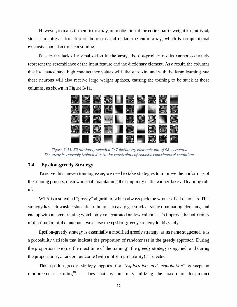
52868
However, in realistic memristor array, normalization of the entire matrix weight is nontrivial,
since it requires calculation of the norms and update the entire array, which is computational
expensive and also time consuming.
Due to the lack of normalization in the array, the dot-product results cannot accurately
represent the resemblance of the input feature and the dictionary element. As a result, the columns
that by chance have high conductance values will likely to win, and with the large learning rate
these neurons will also receive large weight updates, causing the training to be stuck at these
columns, as shown in Figure 3-11.
Figure 3-11: 50 randomly selected 7×7 dictionary elements out of 98 elements. The array is unevenly trained due to the constraints of realistic experimental conditions
3.4 Epsilon-greedy Strategy
To solve this uneven training issue, we need to take strategies to improve the uniformity of
the training process, meanwhile still maintaining the simplicity of the winner-take-all learning rule
of.
WTA is a so-called “greedy” algorithm, which always pick the winner of all elements. This
strategy has a downside since the training can easily get stuck at some dominating elements, and
end up with uneven training which only concentrated on few columns. To improve the uniformity
of distribution of the outcome, we chose the epsilon-greedy strategy in this study.
Epsilon-greedy strategy is essentially a modified greedy strategy, as its name suggested. 𝜖 is
a probability variable that indicate the proportion of randomness in the greedy approach. During
the proportion 1- 𝜖 (i.e. the most time of the training), the greedy strategy is applied; and during
the proportion 𝜖, a random outcome (with uniform probability) is selected.
This epsilon-greedy strategy applies the “exploration and exploitation” concept in
reinforcement learning49. It does that by not only utilizing the maximum dot-product

53868
(exploitation), but also by exploring all neurons to improve the overall decision by randomly
training a column (exploration), which guarantees all the devices are trained in some degree. By
combining both approaches, an improved learning can be achieved.
We simulated the online dictionary learning using our realistic device model with device
parameters extracted from actual devices. Training results with epsilon-greedy strategy were
compared in Figure 3-12, showing similar results with an ideal dictionary learning from the same
training set, and much improved compared with the WTA results in Figure 3-12. In the example
given in this paper, a 49×98, 2× over-complete memristor array was initialized with a Gaussian
distribution of 0.1 mean and 0.13 standard deviation. 𝛽 was chosen so that the pulse widths are in
several µs. 𝜂1 and 𝜂2 were set with 3% and 1% variations respectively. 𝜖 was set to be 0.1 in
learning.
Figure 3-12: Comparison of 49 randomly chosen (a) ideal dictionary elements and (b) dictionary elements trained with ϵ-greedy strategy
3.5 Conclusion
In this chapter, we discussed the consequences of realistic device nonidealities on online
dictionary learning. We investigated the conventional dictionary learning approach via sparse
coding and stochastic gradient descent, which produced good performance but is not very
hardware friendly. Instead, we developed a simpler learning approach with Oja’s rule and winner-
take-all. To address the nonuniform training distribution under realistic experimental constraints,
an epsilon-greedy strategy was proposed. Our simulation results verified the effectiveness of the
learning algorithm, which can produce desired dictionary training using simple WTA without
weight normalization.
(a)
(b)

54868
Chapter 4 Integrated Memristor-CMOS System for Neuromorphic
Computing Applications
In Chapter 2, we successfully demonstrated a sparse coding hardware system in a memristor
crossbar architecture. This approach, based on pattern matching and neuron lateral inhibition, is
an important milestone in the development of large-scale, low power neuromorphic computing
systems. The use of a crossbar architecture allows matrix operations, including matrix-vector dot-
product operation and matrix transpose operations, to be performed directly and efficiently in the
analog domain without the need to read each stored weight. Image reconstruction was also
demonstrated using the memristor system, and online dictionary learning was shown to be feasible
even in the presence of realistic device variations.
Although the key matrix operations can be performed efficiently with memristor crossbar
arrays26,27,42, previous implementations have largely relied on external printed-circuit boards to
provide the required interface and control circuitry23,26,28, or used discrete parameter analyzers to
generate and collect signals22,24,27. In the cases where memristor arrays are integrated with
periphery circuitry, the circuit’s function has been limited to providing access devices (e.g. in the
form of 1T1R arrays23,25,26,42) or address decoding purposes50,51. To demonstrate the potential of
memristor-based computing hardware would require the development of fully functional systems,
where the memristor crossbars are integrated with necessary analog interface circuitry (including
analog-digital converters (ADCs) and digital-analog converters (DACs)), digital buses, and ideally
a programmable processor to control the digital and analog components. Integrating all necessary
functions on-chip will be key to enable practical implementation of memristor-based computing
systems and allow the prototypes to be scaled to larger systems.
In this chapter, we discuss our effort in building a complete neuromorphic computing system,
with memristor crossbar array directly integrated on custom-designed CMOS circuitry that
performs all necessary periphery, neuronal and control functions. The flexibility of the hardware
system in turn allows different algorithms to be implemented on the integrated chip through simple
re-programming.

55868
4.1 CMOS Chip Overview
The integrated memristor/CMOS chip aims to demonstrate all functions, including inference
and online learning, on chip, with the memristor crossbar performing weight storage and vector-
matrix multiplication functions while the CMOS circuitry performing the necessary periphery
functions and signal control.
The CMOS circuitry was designed by collaborators (Justin M. Correll, Dr. Yong Lim,
Vishishtha Bothra and Chester Liu) from Prof. Michael Flynn and Prof. Zhengya Zhang groups.
The CMOS circuitry is essentially an upgraded version of the PCB board setup used in Chapter 2.
The CMOS system are capable of storing and executing C programming independently with the
on chip OpenRISC core, and can apply voltage and read current at each row and column of the
crossbar. This setup allows us to perform all functions of the network on chip, through the hybrid
integrated memristor crossbar and the underlying CMOS circuitry.
4.1.1 System Architecture
The CMOS circuitry mainly consists of three sections (Figure 4-1):
1. 54 + 108 DACs and ADCs, in both row and column directions, which facilitate write and
read operations in both forward and backward directions.
2. On-chip OpenRISC core, which is based on the version used in our previous PCB
measurement setup.
3. Memory blocks, which include a 32k SRAM main memory for instructions and data, and
two 16k ping-pong memory for large data storage.
All three major blocks are connected to a shared system bus, which can transmit data
through an on-chip UART interface to external equipment such as a computer.

56868
Figure 4-1: Layout of the CMOS chip
Blocks showing 54+108 DACs and ADCs, 64k SRAM and an OpenRISC core
Figure 4-2: Chip System Architecture
The integrated memristor/CMOS chip is comprised of the digital controller and bus shown in green, the mixed-signal interface shown in red, and the memristor crossbar shown in blue.
Image credit Justin M. Correll
...
...
...
...
...
...
...
...
...
...
Reg
Reg
Reg
Reg
Re
g
Re
g
Re
g
Re
g
...
...
Custom
Configuration
Registers
and
Timing
Generation
OpenRISC
AltOR32
32Kb SRAM
Instruction
& Data
Data Memory
8Kb SRAM
Ping Pong
Memory
Memory
Controller
UART1
UART2

57868
The CMOS circuitry is schematically shown in Figure 4-2 and Figure 4-3. The on-chip
processor configures the mixed-signal interface through a set of global configuration registers and
performs write and read operations through digital to analog converters (DAC) and analog to
digital converters (ADC).
Since the processor is mainly used for register manipulations, the reduced instruction set
Alternate Lightweight OpenRISC processor (AltOR32) is used in the design to minimize area and
power consumption. The SRAM is divided into 3 parts. The processor instruction and data memory
are mapped to 32k of SRAM and the remaining 32k are multiplexed between two “ping-pong”
memory banks (16k each) for training data buffering. The ping-pong memory banks are dual port
SRAM and can be loaded externally during processing.
The custom mixed-signal interface is shown in Figure 4-3 and includes global timing
generation and configuration registers, and 162 configurable channels – all can write/read to/from
the Wishbone bus (the shared digital bus in OpenRISC architecture) and mapped to the OpenRISC
memory space. Each channel is set to either have an ADC, or 1 of 3 DACs connected to a row or
column of the crossbar. The ADC or DAC connection is set in the mode register and the type of
DAC connections is set in the DAC register along with the 6b DAC pulse input. The timing
generator handles both the ADC start signal and creates the duty-cycled pulse-train for the DACs.
During operation, the processor is first used to configure the mixed-signal interface by
setting the configuration registers. The processor is then paused, and the control is handed off to
the timing generator of the mixed-signal interface. The timing generator operates for 64 cycles
during which VMM operations and memristor weight updates are performed. The control then
goes back to the processor.

58868
Figure 4-3: Mixed Signal Interface design
The mixed-signal interface is comprised of global configuration registers and timing generation shown in brown, and 162 configurable channels (shown in green) to provide input and measure output to and
from each row and column of the memristor crossbar. Image credit Justin M. Correll
4.1.2 Mixed Signal Interface for Crossbar Array
The mixed signal interface is clocked at a slower speed that the OpenRISC core clock.
During the Learning and Inference modes, the OpenRISC controller asserts a GLOBAL_START
signal that starts the mixed signal interface. During this time, the OpenRISC processor is delayed
using NOP commands, and the clocking circuit in the mixed signal interface generates the timing
to control the DACs, ADCs, and crossbar connection configuration.
There are two important registers in the mixed signal interface that provide most of the
critical functions on the chip: configuration register and DAC register.
A global configuration register on the chip controls the write/read mode of all the rows and
columns:
MS_GBL_CFG[2] MS_GBL_CFG[1] MS_GBL_CFG[0]
GBL_START ROW_MODE COL_MODE
Table 4-1: Configuration of the global configuration register
For example, at forward pass mode, all rows are configured as DACs and all columns are
configured as ADCs, so the ROW_MODE is 1 and COL_MODE is 0. At write mode, all rows and
+ -
Virtual
Ground
Read
Write
Erase
Pulses[5:0]
Timing Generator
ADC
DAC Register
13b
9b
Configuration Register
DAC Select
Row Mode Column Mode
DAC
DAC
DAC
6b
Op
en
RIS
C
To
Cro
ss
ba
r
162 Configurable
Channels
ADC Start
Pulse Train
Global Start
Core CLK

59868
columns are configured as DACs, so the ROW_MODE and COL_MODE are both 1.
DAC register is mainly used to configure the pulse generator (for write or read pulses) with
tunable pulse widths. Each pulse generator has the ability to generate a 63-length pulse, with pulse
unit width inversely proportional to the clock speed.
Figure 4-4: Global pulse generator schematic
DAC register is a 9-bit register that holds the voltage selection data and the read/write pulse
durations. The lower 6 bits (DAC_REG [5-0]) specifies the pulse durations and the higher 3 bits
(DAC_REG [8-6]) selects which voltage reference the DAC connects, as shown in Table 4-2. The
register is loaded by the OpenRISC controller via the Wishbone bus. The DAC registers are loaded
serially from their associated (addressed) memory locations.
DAC_REG [8]
DAC_REG [7]
DAC_REG [6]
DAC_REG [5-0]
VWR_H VWR_L VR PULSE_DUR
Table 4-2: Configuration of the DAC register
When all the 9 bits of the DAC register are set to 0, the corresponding row/col is configured
as an ADC (with ROW_MODE or COL_MODE set to 0). In this configuration, when a
GLOBAL_START signal initiates, the pulse generator unit automatically enables the ADC and
perform charge accumulation, controlled by the designed internal logic on the chip.

60868
4.1.3 Four Mode Configurations on the Integrated Chip
The COMS circuit design is flexible and allows the different blocks to be configured into
different modes to facilitate mapping of a complete computing model. Since there are 2 write
DACs, 1 read DAC and a 13-bit ADC at each row or column, the chip can be configured in four
major modes: forward pass mode, backward pass mode, forward write mode (write) and backward
write mode (erase).
When performing VMM, the chip is configured at read mode (forward or backward depends
on the eqaution of the multiplication). During the VMM operation, we apply a discrete-time pulse-
train input and measure the accumulated charge from each column (row). The column (row) ADCs
present a 1.2V virtual ground while the row (column) DACs apply 6-bit programmable train of
fixed-amplitude 0.6V “read” pulses (1.8V-1.2V). The integrating ADCs measure the collected
charge over the input period.
When performing weight update, the chip is configured at write/erase mode (depending on
the need of increase/decrease the weight). During the write operation, we apply discrete-time
pulse-train at both rows and columns. When writing (erasing), the row (column) DACs apply 6-
bit programmable train of fixed-amplitude “write” pulses (1.9V-1V) and the column (row) DACs
apply 6-bit programmable train of fixed-amplitude “erase” pulses (0.1V-1V) with the same
duration, which effectively generate 1.8V (-1.8V) voltage drop across the device. The idle level of
both “write” and “erase” are chosen at 1V, which is the halfway of the voltage drop to provide
write protection for unselected devices in the array.
The configuration of the DAC registers at four different modes and the corresponding pulse
signals are shown in the tables in Figure 4-5 to Figure 4-8. The four different colors of the DAC
registers (red, gray, green and yellow) reprent the corresponding 3 DACs and 1 ADC the register
is used to configure.

61868
Figure 4-5: Forward pass mode on the integrated board
The forward pass mode is used to perform VMM to update the output neurons. In this configuration, all rows are connected to the ‘Read’ DACs, which pulses between 1.2V(VVG) -1.8V(Vread) with the input data represented by different pulse widths, and all columns are connected to 1.2V ADC virtual ground (VVG).
The color table lists the DAC register configuration used to control the “Read” DACs and ADCs.
Figure 4-6: Backward pass mode on the integrated board
The backward pass mode is used for calculating the vector-transposed matrix multiplication. In this configuration, all columns are connected to the ‘Read’ DACs, which pulses between 1.2V(VVG) -1.8V(Vread) with the input data represented by different pulse widths, and all rows are connected to 1.2V ADC virtual
ground (VVG). The color table lists the DAC register configuration used to control the “Read” DACs and ADCs.

62868
Figure 4-7: Write mode on the integrated board
The write mode is used for programming the memristor devices to higher conductance states. In this configuration, all rows are connected to the “Write High” DACs (with range 1V(VHalf)-1.9V(VHigh)) and all columns are connected to the “Write Low” DACs (with range 1V(VHalf)-0.1V(VLow)). The voltage difference
1.8V of the two DACs cross the selected device is used to program the device. The color table lists the DAC register configuration used to control the “Write High” DACs and “Write Low” DACs.
Figure 4-8: Erase mode on the integrated board
The erase mode is used for programming the memristor devices to lower conductance states. In this configuration, all columns are connected to the “Write High” DACs (with range 1V(VHalf)-1.9V(VHigh)) and all rows are connected to the “Write Low” DACs (with range 1V(VHalf)-0.1V(VLow)). The voltage difference -1.8V of the two DACs cross the selected device is used to erase the device. The color table lists the DAC
register configuration used to control the “Write High” DACs and “Write Low” DACs.

63868
4.2 Test Results from the CMOS Circuitry
After the tape-out of the multi-functional CMOS circuitry, we ran serval tests to verify the
basic functions of the circuits. The tests are done in two steps:
1. First, we use a breadboard and some known value resistors to test the basic read functions
of the circuitry, to check the linearity and performance of the on-chip ADCs. We also
probe the voltage waveforms at the terminals that will be connected to the memristors
with an oscilloscope, to verify the operations of read and write mode.
2. After that, an extension board is designed to lead out all the memristor pad signals to a
chip carrier, which is compatible with the previous 32×32 WOx memristor array. More
high-level complex functions like array readout and pattern writing is tested in this
approach.
4.2.1 Verifications of Basic Functions
We first tested the ADC functions by leading the signals from the PCB to a 10k resistor on
the breadboard with jumper wires. By loading a testing C program onto the chip, we can plot the
ADC number (corresponding to the charge collected passing through the resistor) when varying
the applied pulse width from 0 to 63, and obtained a perfect linear curve as shown in Figure 4-9,
which suggests the ADC has excellent linearity vs charge.
0 10 20 30 40 50 60 70
0
500
1000
1500
2000
2500
3000
3500
AD
C n
um
ber
Pulse Width
Forward Read
Backward Read
Figure 4-9: Forward and backward read test with a 10k resistor

64868
We also tested the configuration of the forward pass and backward pass modes. The same
10k resistor is read twice in both forward and backward directions, and the two charge-time curves
are overlapped in Figure 4-9. As can be observed from the plot, both forward and backward
direction ADCs function correctly and generate almost identical results.
To verify the write operations, since a fixed value resistor cannot demonstrate the
programming effect, we use the oscilloscope to monitor the waveform at two terminals of the
resistor.
Figure 4-10: Waveform of two set of write-read pulses pairs. Both write and read pulses have the maximum 63 pulse width.
With the oscilloscope probe on both terminals of the test resistor, we verify the function of
a 63 step-long write pulse followed by a 63 step-long read pulse. While the system is set at the
forward read mode, the yellow waveform probes the selected row and the green waveform probes
the selected column. As shown in Figure 4-10, at the write pulses, the row voltage goes up to Vhigh
(around 1.8V) and the column voltage falls down to around Vlow, (around 0.2V) which creates a
voltage drop of Vhigh - Vlow (around 1.6V) across the device under test (DUT). Note that the actual
Vhigh and Vlow used in the memristor experiment is 1.9V and 0.1V, to create the programming
voltage required by the devices.

65868
Figure 4-11: Zoomed-in waveform of the write pulses Both write and read pulses have the maximum 63 pulse width
Figure 4-11 shows a zoomed-in waveform of the 63-step long writing pulses. As can be
observed from the waveform, instead of directly modulating the pulse width, we use the number
of pulses to represent the input amplitude (effectively modulating the pulse width in discrete time
domain) to eliminate errors due to pulse rise and fall time.
4.2.2 Results with Extension Board and Stand-alone Memristor Array
Although we can verify some basic functions by observing the waveform output, a better
approach is to connect the circuit output to real memristor devices and verify the read/write
operations. An ideal approach is direct integration of the memristor onto the CMOS circuit, which
will be discussed in section 4.3.
In particular, since the direct integration of memrsitor arrays on the CMOS chip is a
challenging process, to separate potential issues from the fabrication process or the CMOS design
it will be very useful to perform some preliminary test with a stand-alone memristor array which
we already know functions properly.
Based on this idea, we designed an extension board which can interface a standalone
memristor crossbar array with the CMOS chip (Figure 4-12). We lead out all output control signals
generated by the CMOS chip and feed them to the extension board, which serves as a routing board

66868
to send the control voltages to the memristor array on the chip carrier. This approach is compatible
with the previous testing setup discussed in Chapter 2 and we can reuse our 32×32 memristor
arrays.
Figure 4-12: Main testing board (blue) and extension board (green).
With the extension board plugged in, we can verify the programming and erasing function
with a previous working memristor array. We applied 200 writing and erasing pulse to a single
device on the corner of a stand-alone memristor array. Figure 4-13 shows successful gradual
conductance increase and decrease obtained through signals generated and collected from the
CMOS circuitry using this setup.

67868
Figure 4-13: Pulse program and ease curve of a single memristor device on a stand-alone chip.
Moreover, since the extension board lead out 32 row and 32 column signals from the CMOS
chip and connected to the socket on the extension board, we are able to verify array operations
with the extension board for the 32×32 array. We verified fundamental array operations such as
pattern programming and array read-out, which enabled us to write grayscale images into the array,
with a couple of examples shown in Figure 4-14.
Figure 4-14: Patterns written with extension board.
A 4×4 checkerboard pattern and an “M” pattern written and read out from the memristor array using the CMOS chip.
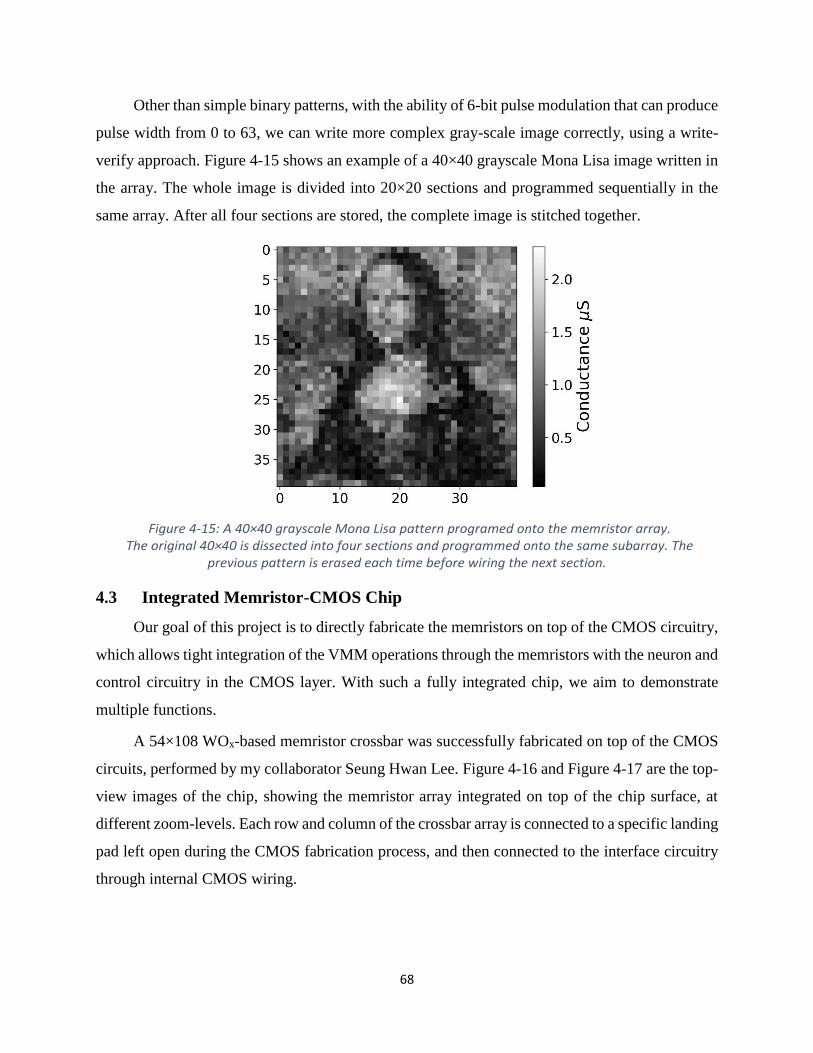
68868
Other than simple binary patterns, with the ability of 6-bit pulse modulation that can produce
pulse width from 0 to 63, we can write more complex gray-scale image correctly, using a write-
verify approach. Figure 4-15 shows an example of a 40×40 grayscale Mona Lisa image written in
the array. The whole image is divided into 20×20 sections and programmed sequentially in the
same array. After all four sections are stored, the complete image is stitched together.
Figure 4-15: A 40×40 grayscale Mona Lisa pattern programed onto the memristor array. The original 40×40 is dissected into four sections and programmed onto the same subarray. The
previous pattern is erased each time before wiring the next section.
4.3 Integrated Memristor-CMOS Chip
Our goal of this project is to directly fabricate the memristors on top of the CMOS circuitry,
which allows tight integration of the VMM operations through the memristors with the neuron and
control circuitry in the CMOS layer. With such a fully integrated chip, we aim to demonstrate
multiple functions.
A 54×108 WOx-based memristor crossbar was successfully fabricated on top of the CMOS
circuits, performed by my collaborator Seung Hwan Lee. Figure 4-16 and Figure 4-17 are the top-
view images of the chip, showing the memristor array integrated on top of the chip surface, at
different zoom-levels. Each row and column of the crossbar array is connected to a specific landing
pad left open during the CMOS fabrication process, and then connected to the interface circuitry
through internal CMOS wiring.

69868
Figure 4-16: Microscopic image of the integrated chip. Some testing structure were made for testing.
Figure 4-17: Zoomed-in microscopic image of the integrated chip. Inset: SEM image of the crossbar array.
The memristor crossbar array used in this work is directly fabricated on top of the CMOS
circuits. First, the bottom electrode (BE) patterns with 500 nm width are defined by e-beam
lithography, the 80nm think Au BEs are then deposited (with Ni/Cr adhesion layer underneath) by

70868
e-beam evaporation and lift-off processes. Next, 300 nm of SiO2 is deposited by plasma-enhanced
chemical vapor deposition (PECVD), followed by RIE etch back to form a spacer structure along
the sidewalls of the BEs. The spacer structure allows better step coverage for the WOx switching
layer and the top electrodes (TEs) at the crosspoints, and also restricts the active device regions to
the flat exposed top surface of the BEs, as shown in Figure 4-18. To prevent leakage through the
switching layer among adjacent devices, the switching layer is only deposited at the crosspoint
regions through patterns defined by e-beam lithography. The switching layer is formed by first
depositing 20nm think W through DC sputtering and lift-off processes in the e-beam patterned
regions, then through rapid thermal annealing of the patterned W islands with oxygen gas at 400°C
for 60s to form the WOx switching material. Afterwards, the TEs (Pd (40 nm)/Au (90 nm)) with
500nm width are patterned and deposited by e-beam lithography, e-beam evaporation, and liftoff
processes. Finally, metallization processes are performed by photolithography (GCA AS200
AutoStep) to connect the crossbar electrodes with the CMOS landing pads that are left open during
the CMOS circuit fabrication process. An in-situ etch process is performed to remove the native
aluminum oxide on the CMOS landing pads, followed by deposition of 800nm thick Al with DC
sputtering and lift-off processes to ensure step coverage of the deeply recessed landing pads.
Figure 4-18: A cross-section schematic of the integrated chip Showing connections of the memristor array with the CMOS circuitry through extension lines and
internal CMOS wiring. Inset: cross-section of the WOx device
The integrated memristor/CMOS chip is wire-bonded onto a pin-grid-array (PGA) package
(Figure 4-19) and mounted on a PCB (Figure 4-20). The PCB provides essential power signals and

71868
the global system clock to the integrated chip. No active circuitry (DACs, ADCs, matrix switch
etc.) are implemented on the PCB, as these functions are all provided on-chip directly. A UART-
to-serial (UART: universal asynchronous receiver-transmitter) board converts the IO data from the
chip into serial data and communicate a desktop computer through a USB cable.
Figure 4-19: Integrated chip after wire bonding and packaging. The chip is wire-bonded on a pin-grid-array (PGA) package, which can be plugged into a socket on the
PCB board.
Figure 4-20: Testing set-up used to power and test the integrated memristor/CMOS chip. The left green board is used to filter the power signal for ADC input. The wire bonded chip is plugged
into a socket on the blue PCB board on the right. The top small board is a UART-to-serial board.

72868
The integrated WOx devices show similar I-V characteristics as standalone WOx arrays such
as those shown in Figure 1-6. It can demonstrate typical potentiation and depression curves with
consecutive programming and erasing pulses, such as those in Figure 4-21 for four different
devices from the integrated memristor array.
0 100 2000.8
1.0
1.2
1.4
1.6
1.8
2.0
2.2
2.4
0 100 2001.2
1.4
1.6
1.8
2.0
2.2
2.4
2.6
2.8
0 100 200
1.2
1.4
1.6
1.8
2.0
2.2
2.4
2.6
2.8
3.0
0 100 200
1.2
1.4
1.6
1.8
2.0
2.2
2.4
2.6
2.8
Cu
rre
nt
(A
)
Pulse NumberC
urr
en
t (
A)
Pulse Number
Cu
rre
nt
(A
)
Pulse Number
Cu
rre
nt (
A)
Pulse Number
Figure 4-21: Programming and erasing memristors on chip
Weight update curves from four memristor devices measured from the crossbar array in the integrated chip. The devices were programmed by 50 write pulse at 1.8V and 50 erase pulses at -1.8V, with 82µs
pulse width, using the on-chip processor and the integrated DAC/ADC circuitry.
4.4 Single Layer Perceptron for Greek Letters Classification
To verify the operation of the integrated memristor/CMOS chip, we first implemented a
feed-forward single-layer perceptron (SLP) network. 5×5 binary patterns are used in the SLP
training and testing.
The SLP has 26 inputs (corresponding to the 25 pixels in the image and a bias term) and 5
outputs, with the input and output neurons fully connected with 26×5 = 130 synaptic weights. The
weighted sums are then calculated with a nonlinear activation function --- the classical “Softmax”
function (will be discussed later). The final output values of the neurons are in the range 0~1,

73868
where the neuron with the highest output is identified as the winner and used to classify the
corresponding class, as schematically shown in Figure 4-22.
Figure 4-22: Implementation of the SLP using a 26×10 memristor array through the integrated chip. a. Schematic of the single-layer perceptron for classification of 5×5 images. b. The input data (e.g. Greek Letter ‘Ω’) are converted to voltage pulses of Vread or 0 through circuitry, depending on the pixel value.
In this experiment, the original binary input patterns are converted into input voltage pulses
through the integrated processor and DAC circuitry and are fed to the rows of the memristor array.
Specifically, when a white pixel is present, a pulse is applied to the corresponding row; while black
pixels correspond to no pulse. The bias term is fixed at a constant value of 1 (treated as a white
pixel) and is applied as an extra input. All the input pulses have the same duration and amplitude
in this test, as illustrated in Figure 4-22.
Each synaptic weight 𝑤𝑖𝑗 is implemented with two memristors representing a positive and a
negative weight, 𝐺𝑖𝑗+ and 𝐺𝑖𝑗
−, respectively, using the positive memristor conductance values. The
charge collected at an output neuron j is determined as:
𝑄𝑗 = ∑ 𝑤𝑖𝑗𝑥𝑖
𝑖
= 𝑉 ∑ 𝐺𝑖𝑗𝑡𝑖
𝑖
= 𝑉 ∑(𝐺𝑖𝑗+ − 𝐺𝑖𝑗
−)𝑡𝑖
𝑖
= 𝑄𝑗+ − 𝑄𝑗
− (4 − 1)
Where 𝑥𝑖 is the input at row i and represented by a voltage pulse with amplitude V and width
𝑡𝑖. The charges are measured at the output columns and digitized by the ADCs, then converted to
the neuron output 𝑦𝑗 through the Softmax function:

74868
𝑦𝑗(𝑄𝑗) =exp(𝛽𝑄𝑗)
∑ exp(𝛽𝑄𝑘)𝑘 (4 − 2)
where 𝛽 is a scaling number of the ADC output and 𝑘 represents the output neuron index
The integrated chip allows us to perform online learning. Specifically, the synaptic weights
are updated during the training state using the batch gradient descent rule:
Δ𝑤𝑖𝑗 = 𝜂 ∑(𝑡𝑗(𝑛)
− 𝑦𝑗(𝑛)
)𝑥(𝑛)
𝑁
𝑛=1
(4 − 3)
where 𝑥(𝑛) is the nth training sample of the input dataset, 𝑦(𝑛) is the network output and 𝑡(𝑛)
is the corresponding label, 𝜂 is the learning rate. The update value Δ𝑤𝑖𝑗 for the ith element in the
jth class is then implemented in the memristors by applying programming pulses through the write
DACs with a pulse width proportional to the desired weight change (quantized within the range of
0~63 timesteps, i.e. corresponding to 6-bit precision).
The SLP is mapped on the integrated chip using a 26×10 subarray. We trained and tested
the SLP with noisy 5×5 Greek Letter patterns, for 5 distinct classes: ‘Ω’, ‘Μ’, ‘Π’, ‘Σ’, ‘Φ’. For
each Greek letter, we flip one of the 25 pixels of the original image and generate 25 noisy images.
Together with the original image they form a set of 26 images for each letter. We randomly select
16 images from the set for each class for training and use the other 10 images for testing. An
example of the training set and testing set is shown in Figure 4-23 and Figure 4-24. This approach
guarantees that the training set and the testing set do not overlap, and therefore improves the
robustness of our testing results, since the noisy test images are not used to train the network.
Figure 4-23: Noisy training data set for the SLP.
The training data set for each class includes the original image and 15 out of the 25 noisy images created by flipping 1 pixel in the original image.

75868
Figure 4-24: Noisy testing data set for the SLP.
The testing data set includes the 10 noisy images not in the training set, created by flipping 1 pixel in the original image for each class.
Training and testing results from the experimentally implemented SLP are shown in Figure
4-25 and Figure 4-26. After 5 online training epochs the SLP can already achieve 100%
classification accuracy for both the training and testing sets. The average activation of the correct
neuron during training is also clearly separated from the others, and the difference in neuron
outputs between the winning neuron and the other neurons improves during training, as shown in
Figure 4-25, verifying online learning has been reliably implemented in the experimental setup.
Compared with earlier SLP implementations22 that used the Manhattan rule and required on
average 23 epochs to achieve perfect classification for a similar database, batch gradient descent
used here not only considers the direction of the weight update (which is the case with the
Manhattan rule), but also the value of weight update, so that much faster training convergence can
be obtained, as shown in Figure 4-26.
0 5 10 15 20 25 30
0.1
0.2
0.3
0.4
0.5
0 5 10 15 20 25 30 0 5 10 15 20 25 30 0 5 10 15 20 25 30 0 5 10 15 20 25 30
y
Epochs Epochs Epochs Epochs Epochs
Figure 4-25: Evolution of the output neuron signals during training, averaged over all training patterns for a specific class
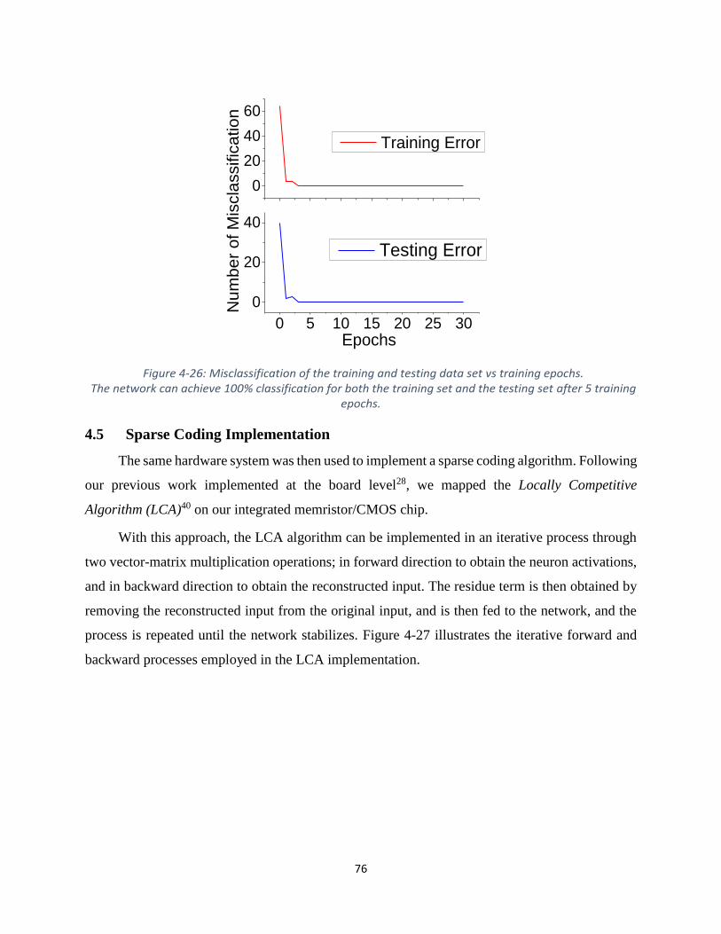
76868
0
20
40
60
0 5 10 15 20 25 30
0
20
40N
um
be
r o
f M
iscla
ssific
atio
n
Training Error
Epochs
Testing Error
Figure 4-26: Misclassification of the training and testing data set vs training epochs. The network can achieve 100% classification for both the training set and the testing set after 5 training
epochs.
4.5 Sparse Coding Implementation
The same hardware system was then used to implement a sparse coding algorithm. Following
our previous work implemented at the board level28, we mapped the Locally Competitive
Algorithm (LCA)40 on our integrated memristor/CMOS chip.
With this approach, the LCA algorithm can be implemented in an iterative process through
two vector-matrix multiplication operations; in forward direction to obtain the neuron activations,
and in backward direction to obtain the reconstructed input. The residue term is then obtained by
removing the reconstructed input from the original input, and is then fed to the network, and the
process is repeated until the network stabilizes. Figure 4-27 illustrates the iterative forward and
backward processes employed in the LCA implementation.

77868
Figure 4-27: Schematic of the LCA algorithm using integrated chip. In each iteration a forward pass is performed to update the membrane potential u of the output
neurons based on the inputs, followed by a backward pass to update the residual r based on the neuron activities a. The residual r term forms the input for the next iteration.
The bi-directional operation of the memristor array in the integrated memristor/CMOS chip
allowed us to experimentally implement the sparse coding algorithm on chip. Similar to the SLP
case, we use the crossbar array to perform VMM operations, here in both forward and backward
directions. Since the chip offers full flexibility to implement different algorithms by re-
programming the integrated processor, the LCA algorithm was implemented in the same chip used
in the SLP study, through simple software changes.
4×4 inputs were used to test the experimental implementation of the LCA algorithm. By
using linear combinations of horizontal and vertical bar patterns, the input dimension is reduced
to 7. To satisfy the over-completeness requirement of the LCA algorithm, a dictionary containing
14 features of horizontal and vertical bar patterns are used, as shown in Figure 4-28a. This setup
produces a 2× over-complete dictionary40 that enables the network to find a sparse, optimal
solution out of several possible solutions.

78868
Figure 4-28: Experimental demonstration of sparse coding using the integrated memristor chip a) Dictionary elements based on horizontal and vertical bars. b) The original test image. c) The experimentally reconstructed image based on the neuron activities from the memristor chip. d)
Experimentally obtained neuron membrane potentials as a function of iteration number during LCA
analysis. The red horizontal line marks the threshold parameter .
The LCA algorithm was mapped to a 16×14 subarray in the memristor/CMOS chip, using
the integrated corresponding interface circuitry and the processor that provide the neuron
functions. An example of the LCA network operation is shown in Figure 4-28 (b-d). The
experimentally implemented network correctly reconstructs the input image while minimizing the
number of activated neurons. For example, it identifies the optimized solution with two neurons 6
and 13, instead of using three neurons 2,4 and 6. Examining the dynamics of the network operation
also verified the successful LCA implementation. As shown in Figure 4-28d, all neurons are
charging up in the first 4 iterations. At the 5th iteration, neuron 13 first crosses the threshold, since
it consists of two horizontal bars and results in a larger output value in the membrane potential
update. As a result, the lateral inhibition effect in the system suppresses the membrane potentials
of other neurons (2 and 4) sharing part of the patterns with neuron 13, even though they also
represent features of the input. Meanwhile neuron 6 which represents the vertical bar feature
continues to charge up. At iteration 11, neuron 6’s membrane potential crosses the threshold and
all other neurons’ membrane potentials are suppressed below the threshold, leading to the finding
of the optimal solution. The neurons’ membrane potentials continue to evolve but those of neuron
6 and 13 remain above the threshold and those of other neurons continue to decrease due to the
inhibition term and the leaky term in the membrane potential equation, and the solution from the
network was read out after 30 iterations.

79868
To verify the system’s performance for other input patterns, an exhaustive test of all 24
possible patterns consisting of two horizontal bars and 1 vertical bar was performed using the on-
chip memristor network, resulting in 100% success rate (Figure 4-29) measured by the network’s
ability to correctly identify the sparse solutions.
Figure 4-29: Additional examples of input images and reconstructed images.
The same threshold = 18 is used in all images.
4.6 Principal Component Analysis with Bilayer Networks
Finally, we demonstrate a bilayer neural network using two subarrays in the same memristor
crossbar, implementing unsupervised and supervised online learning to achieve feature extraction
and classification functions, respectively. The bilayer network is used to analyze and classify data
obtained from breast cancer screening based on principal component analysis (PCA). Specifically,
the first layer of the system is a 9×2 network that performs PCA of the original data, which reduces
the 9-dimensional raw input data to a 2-dimensional space based on the learned principal
components (PCs). The second layer is a 3×1 SLP layer (with differential weights and a bias term)
which performs classification using the reduced data in the 2-dimensional space for the two classes
(benign or malignant). The schematic and crossbar implementation of the bilayer network is shown
in Figure 4-30.

80868
Figure 4-30: Implementation of the bilayer network on the integrated chip a) Schematic of the bilayer neural network for PCA analysis and classification. b) The bilayer network is
mapped onto the integrated memristor chip, using a 9×2 subarray for the PCA layer and a 3×2 subarray for the classification layer
PCA reduces data by projecting them onto lower dimensions along principal components,
with the goal of finding the best summary of the data using a limited number of PCs52. The
conventional approach to PCA is to solve the eigenvectors of the covariance matrix of the input
data, which can be computationally expensive in hardware. A more hardware-friendly approach is
to find the PCs through unsupervised, online learning.
Specifically, following our previous study30, Sanger’s rule, also known as the generalized
Hebbian algorithm, is implemented in the integrated chip to obtain the PCs. The desired weight
change for the jth principal component is determined by:
𝛿𝑔𝑖𝑗 = 𝜂𝑦𝑗 (𝑥𝑖 − ∑ 𝑔𝑖𝑗𝑦𝑗
𝑗
𝑘=1
) (4 − 4)
4.6.1 Mapping memristor conductance to synaptic weight in PCA
In the experiment, the weights of the 1st and 2nd PCs, 𝑔𝑖𝑗, are mapped onto the memristor
conductances through a linear transformation with range ([-1 1]), by using the relationship:
𝑔 =𝐴𝐷𝐶 − 𝑎
𝑏 (4 − 5)
where ADC is the unconverted ADC output from the circuit, which is converted to the
current/conductance value through factors a (ADC shift factor, which is about 1900) and 𝑏 (ADC
scaling factor, which is about 1500) in Equation (4-5). The conversion based on Equation (4-5)

81868
maps the maximum average current to weight 1 and minimum average current to weight -1.
For each input data, the dot-product of the input data and the jth feature, 𝑦𝑗 is directly
obtained from the ADC output of the jth column of the 9×2 weight matrix. The column’s weights
are then updated from the Sanger’s rule in Equation (4-4)
During training, the desired weight updates are linearly converted into write pulse widths
and applied to the memristor devices, without using nonlinear compensation schemes such as the
one discussed. Device nonidealities including the nonlinear weight updates (as shown in Figure
4-21) caused the experimentally obtained training results to differ from the software results.
4.6.2 Training the 1st Layer for Principal Component Analysis
The network is trained online, using a subset of the original database consisting of 100 data
points. During the training process, the 9-dimensional breast cancer data is converted into input
voltage pulses with pulse widths proportional to the data values, within the range of 0~63 time
units. The output charge collected at column j then corresponds to the dot-product of the input
vector and the conductance vector stored in column j, projecting data from the original 9-
dimensional space to a 2-dimensional output space (when only two principal components are
used). During training, the weights are then updated following Equation (4-4), using programming
voltage pulses generated through the write DACs with pulse widths proportional to 𝛿𝑔𝑖𝑗.
Initially, the weights of the 1st and 2nd components are randomized in the memristor array
(Figure 4-31a). Projection of the input along these vectors leads to severe overlapping of the benign
and malignant cases in the 2-dimensional space, as shown in Figure 4-31b and Figure 4-31c. After
30 training epochs (an epoch is defined as a training cycle through the 100 training data), the PCs
are correctly learned (Figure 4-32a), and the 2-dimensional projected data can be clearly separated
into two clusters, as shown in Figure 4-32b and Figure 4-32c. Note the ground truth (benign or
malignant) is not used in the PCA training or clustering process. They are included in the plots
(represented as blue and red colors) only to highlight the effectiveness of the clustering before and
after learning the PCs.

82868
Figure 4-31: Weight and data distribution before PCA. a) Initial weights for the two PCs in the network. Before training, linear separation is not possible in the
projected 2-dimenstional space, for both training (b) and testing data (c).
Figure 4-32: Weight and data distribution after PCA. a) Weights for the two PCs after unsupervised, online training obtained from the memristor network,
using Sanger’s learning rule for 30 cycles of training. Clear separation can be observed in the 2-dimenstional space for both training (b) and testing (c) data after projection along the trained PCs.
The PCA layer separate the original data into clusters, but does not classify them. To achieve
classification, we implemented a second layer, a SLP, in the same hardware system. The on-chip
DACs offer 6-bit resolution and can generate pulses of range 0~63. However, after the PCA
process, the 2-D projected data have analog and negative values. To use the PCA output data as
input to the second, perceptron layer, we need to rescale the data to the range of 0~63 and quantize
them into pulse numbers.
4.6.3 Scaling of the PCA layer output as perceptron layer input
As can be observed from Figure 4-32, most of the PCA output data are located in the range
of 3~25 in the x axis and -15~3 in the y axis. To quantize and scale the data to the range of 0~63
for the perceptron layer, the following formulas are used:

83868
= 𝑟𝑜𝑢𝑛𝑑[2𝑥] (4 − 6𝑎)
= 𝑟𝑜𝑢𝑛𝑑[−3(𝑦 − 3)] (4 − 6𝑏)
Notice that some outlier data points would produce values larger than 63. These few points were
mapped to 0 pulses so that all other points can make use of as much dynamic range of 0~63 as
possible.
After quantization and scaling, the data are classified using the perception layer, and the
results are shown in Figure 4-33. The labels are directly obtained from the neuron outputs in the
perceptron layer, without reading the weight values. Finally, data were replotted in the original
PCA output space, using the obtained corresponding label for each data point, as shown in Figure
4-34.
5 10 15 20 25 30 35-10
0
10
20
30
40
50
Memristor Predicted Benign
Memristor Predicted Malignant
Convert
ed 2
nd P
C P
roje
ction
Converted 1st PC projection
Figure 4-33: Classification of the quantized data.
Outputs from the PCA layer were quantized and scaled to the range of 0~63, and used as input to the second perceptron layer. The quantized data were then classified by the perception layer, with blue
points representing the network classified benign data and red points representing the network classified malignant data.

84868
4 6 8 10 12 14 16 18-16
-14
-12
-10
-8
-6
-4
-2
0
2
4
6
Memristor Predicted Benign
Memristor Predicted Malignant
2nd P
rincip
al C
om
ponent P
roje
ction
1st Principal Component Projection
Figure 4-34: Replotted classification results in the original space.
The classified results in Figure 14 were then replotted in the original output space from the PCA layer, with blue points representing the network classified benign data and red points representing the
network classified malignant data.
4.6.4 Training of the 2nd perceptron layer for classification
The SLP processes outputs from the PCA layer and generates a label (benign or malignant).
Since there are only two classes to distinguish, the SLP is trained online using logistic regression.
A 3×2 subarray is used in the second layer, to account for the 2 inputs, the bias term, and the
differential weights.
The training rule based on logistic regression using batch gradient descent has a similar
format as the Softmax regression used in Equation (4-7):
Δ𝑤𝑖 = 𝜂 ∑(𝑡(𝑛) − 𝑦(𝑛))𝑥𝑖(𝑛)
𝑁
𝑛=1
(4 − 7)
where 𝜂 is the learning rate, 𝑦(𝑛), 𝑡(𝑛), 𝑥(𝑛) are the neuron outputs, ground truth label and
input data for the nth input sample.
After learning the PCs in the PCA layer, the original 9-dimensional data are fed through the
PCA layer, and the clustered 2-dimensional data are used as inputs for the SLP layer. The same
100 training data used for the PCA layer training are used for the SLP layer training (Figure 4-35),
in a supervised fashion using the ground truth (the label associated with the original data). Training
is completed after 30 epochs.

85868
0 10 20 30
0
5
10
15
20
25
30
35
40
45
50
55
Nu
mb
er
of
Mis
cla
ssific
atio
n
Training Epochs
Figure 4-35: Evolution of the number of misclassifications during the online training process
Afterwards, the 500 test data not included in the training set are applied to the network,
passing first through the PCA layer then as 2-dimentional data into the 2nd SLP layer. After online
training of the PCA and the SLP layers, the experimentally implemented 2-layer network can
achieve 94% and 94.6% classification accuracy during training and testing (Figure 4-36). The
values are slightly lower than the ones obtained from software implementation (95% during
training and 96.8% during testing, Figure 4-37), due to the nonideality in the memristor weight
update that results in a decision boundary that differs from that obtained from software (which
assumes ideal linear weight updates) after the online training process. We expect future device
optimizations that can improve device weight update linearity25,53 will further improve the network
performance and enable large scale practical hardware implementations.

86868
Figure 4-36: Classification results experimentally obtained from the memristor chip. The blue and red colors represent the predicted benign and malignant data, respectively. The incorrectly
classified results are marked as hollow circles. Classification rates of 94% and 94.6% are obtained for the training (a) and testing (b) data, respectively
Figure 4-37: Classification results of the bilayer network implemented in software. The blue and red colors represent the predicted benign and malignant data, respectively. The incorrectly classified results are marked as hollow circle. Classification rates of 95% and 96.8% are obtained for the
training (a) and testing (b) data in software, respectively.

87868
4.7 Power Analysis and Estimation
The power consumption of the integrated memristor/CMOS system consists of three parts:
the digital OpenRISC core, the mixed signal interface, and the power consumed by the passive
crossbar array.
Both the digital processor power and mixed signal interface power are directly measured
experimentally, by measuring the root mean square (RMS) current with a Fluke meter while
running the chip, with the help of Justin M. Correll from Prof. Michael P. Flynn’s group. At the
maximum frequency of 148MHz, the digital power reads 235.3mW and the total analog power
reads around 64.4mW. The crossbar array power is obtained from the average device current at
the read voltage, which yields ~7mW for the 54×108 array. The total power at 148MHz clock is
thus 306.7mW for the current chip based on 180nm CMOS technology.
The energy efficiency is estimated using the 148MHz clock speed and an average 4-bit input
during inference, which gives around 9.4M VMM operations per second. Multiplying this number
by 54×108 lead to 5.48×10¹⁰ operations per second. Therefore, the energy efficiency can be
derived by dividing the number of ops/second with the total power, which results in 178.68
GOPS/W for the current memristor/CMOS chip.
The custom circuitry was designed in 180nm CMOS and features a generic digital processor
along with a full set of mixed signal analog to digital converters (ADC) and digital to analog
converters (DAC). Two different approaches were used to estimate the power dissipation at the
40nm technology node. The digital power was estimated using generalized scaling54 and the
mixed-signal power was estimated using a figure of merit (FOM) approach.
In digital circuits, the length scaling factor S, and the supply voltage scaling factor U are
different during scaling. We chose the generalized scaling approach for digital power.
Specifically, from 180nm to 40nm, S = 180nm/40nm = 4.5, U = 1.8V/1.0V = 1.8. As a result,
the digital power is reduced by a factor of 1/U2 = 0.32, while the circuit speed is improved by a
factor of S = 4.5. Note the faster processor allows the same process to control more channels, so
normalizing to the same number of 162 channels, the digital power at 40nm is estimated to be
𝑃40𝑛𝑚 =𝑃180𝑛𝑚
𝑈2𝑆 (4 − 8)
Using the measured digital power at 180nm, the estimated digital power at 40nm is then

88868
235.3mW/((1.8)2×4.5), which is about 16.1mW.
Figure 4-38: Schreier FOM for 180nm and 40nm ADCs published in ISSCC and VLSI conferences from 1997-2018.
The Schreier FOM is used for comparing high-resolution ADC performance across architectures. Image credit: Justin M. Correll
The analog to digital converter performance is evaluated using various figures of merit
(FOM). An ADC FOM combines several converter performance metrics into one number for
comparison across ADC architectures. The Schreier FOM is typically used for high-resolution
converters and is given by the following equation:
𝐹𝑂𝑀𝑠 = 𝑆𝑁𝐷𝑅 + 10 log (𝐵𝑊
𝑃) (4 − 9)
where SNDR is the signal to noise ratio and distortion, BW is one-half of the sampling
frequency, and P is the power dissipation. To estimate the power scaling from 180nm to 40nm,
the ADC Performance Survey55 was used which aggregates all ADCs published in the ISSCC and
VLSI circuits conferences from 1997 - 2018. A subset of data for 180nm and 40nm ADCs is shown
in Figure 4-38. The mean FOM between sampling frequencies from 100kHz to 10MHz for each
technology was determined and compared. The mean FOM for 40nm was determined at 172dB
and a conservative estimate of 165dB was used for power estimation. Using an estimated 165 dB,

89868
which corresponds to 176W per ADC, we can get the new total analog power at 40nm is 19mW,
leading to a total system power of 42.1mW, assuming the 54×108 crossbar power remains at 7mW.
Therefore, by simply scaling the system to 40nm technology node, the estimated OPS/W at
148MHz is 1.3TOPS/W. The power efficiency can be further improved by further scaling the
CMOS circuit to more advanced technology nodes. Additionally, the digital power can be further
improved by using a more custom controller design instead of using a generic processor, while the
analog power can be improved by further optimizations of the ADC circuitry (e.g. replacing the
fast and high-precision 13-bit ADC with simpler interface circuits), along with memristor device
optimizations to reduce the crossbar power.
4.8 Conclusion
In this chapter, we successfully designed and fabricated a fully-functional, programmable
neuromorphic computing chip with a passive memristor crossbar array directly integrated with a
complete set of analog and digital components and an on-chip processor. The integrated chip
allows mapping of different neuromorphic and machine learning algorithms on chip through
simple software changes. Three different and commonly-used models, perceptron, sparse coding
and principal component analysis with an integrated classification layer, were demonstrated. 100%
classification accuracy was achieved for 5×5 noisy Greek Letters in the SLP implementation,
reliable sparse coding analysis was obtained from an exhaustive test set using 4×4 bar patterns,
and 94.6% classification rate was experimentally obtained from the breast cancer screening dataset
using the same integrated chip.
The integrated chip suggests different computing tasks can be efficiently mapped on the
memristor-based computing platform, by taking advantage of the bidirectional VMM operations
in the memristor crossbars and the flexibility in the CMOS interface and control circuitry. In our
prototype, the supporting analog interfaces, as well as digital control and the OpenRISC processor
are implemented in 180nm CMOS technology.
The entire mixed-signal interface with independent ADCs and DACs supporting the 54×108
crossbar and operating at the maximum frequency of 148 MHz consumes 64.4 mW from the
experimental measurements. This corresponds to energy consumption of 27.4 nJ/inner product or
4.7 pJ/op for the mixed-signal interface, where an operation is defined as the multiplication and

90868
accumulate (MAC) process of a 4-bit input with a stored analog weight in the memristor array. At
the maximum operating frequency of 148 MHz, the total system power of 306.7 mW and a power
efficiency of 178.68 GOPS/W for the experimentally demonstrated memristor/CMOS chip based
on 180 nm CMOS technology. Simply scaling the design to a more advanced process node such
as 40 nm CMOS technology the power efficiency 1.3 TOPS/W can be achieved. We believe further
optimizations of the system design, e.g. by replacing the generic processor with a custom-designed
controller, and by replacing the fast and high-precision 13-bit ADC with simpler interface circuits,
along with memristor device optimizations that reduce power consumption in the memristor
crossbar, can further improve the system’s performance and power efficiency.

91868
Chapter 5 Reservoir Computing with Memristor Devices
The previous studies from Chapter 2 to Chapter 4 mainly focus on using memristor crossbar
structures to act as a matrix operation accelerator to implement neural network applications such
as sparse coding or feedforward networks. However, dynamic memristor behaviors discussed in
Chapter 1 can also be used to natively perform other computing tasks. One interesting and important
application is reservoir computing (RC), where the short-term memory effect of memristors can be
utilized for efficient temporal information processing.
In this study, we experimentally demonstrate a memristor-based RC system using dynamic
memristor devices that offer internal, short-term memory effects17,56,57. These dynamic effects
allow the devices to map temporal input patterns into different reservoir states, represented by the
collective memristor resistance states, which can then be further processed through a simple
readout function. The memristor-based RC hardware system is then used to experimentally
perform hand digit recognition tasks and solve a 2nd-order nonlinear task.
5.1 Reservoir Computing
Reservoir Computing (RC) is a novel neural network-based computing paradigm that allows
effective processing of time varying inputs58–60. An RC system is conceptually illustrated in Figure
5-1, and can be divided into two parts: the first part, connected to the input, is called the reservoir.
The connectivity structure of the reservoir will remain fixed at all times (thus requiring no
training), however, the neurons (network nodes) in the reservoir will evolve dynamically with the
temporal input signals. The collective states of all neurons in the reservoir at time t form the
reservoir state x(t). Through the dynamic evolutions of the neurons, the reservoir essentially maps
the input u(t) to a new space represented by x(t) and performs a nonlinear transformation of the
input. The different reservoir states obtained are then analyzed by the second part of the system,
termed the readout function, which can be trained and is used to generate the final desired output
y(t). Since training a RC system only involves training the connection weights (red arrows in the

92868
figure) in the readout function between the reservoir and the output61, training cost can be
significantly reduced compared with a conventional recurrent neural network (RNN) approaches61
Figure 5-1: Schematic of an RC system, showing the reservoir with internal dynamics and a readout function
The readout function in an RC system is typically simple (thus easy to train) and is normally
based on a linearly weighted combination of the reservoir neuron node values. As a result, it is
memory-less. To process temporal information, the reservoir state needs to be determined not only
by the present input but also by inputs within a certain period in the past. Therefore, the reservoir
itself must have short-term memory. In fact, it has been mathematically shown60 that a RC system
only needs to possess two very unrestrictive properties to achieve universal computation power
for time-varying inputs: point-wise separation property for the reservoir, which means that all
output-relevant differences in the input series u1() and u2() before time t are reflected in the
corresponding reservoir internal states x1() and x2() that are separable; and approximation property
for the readout function, which means that the readout function can map the current reservoir state
to the desired current output with required accuracy.
5.2 Short-term Memory WOx Memristor as Reservoir
In this study, memristor devices with short-term memory effects17,56,57 were used to act as
the reservoir in an RC system. During device fabrication, the switching layer of the WOx based
device was specifically designed to exhibit short-term memory (i.e. volatile) behavior17,56,57
To demonstrate the temporal dynamics of the device, a pulse stream composed of write
pulses having the same amplitude (1.4 V, 500 µs) but at different timeframes are applied to the

93868
device and the response of the memristor, which is represented by the read current through a small
read pulse (0.6 V, 500 µs) following each write pulse, is recorded. The results are shown in Figure
5-2.
Figure 5-2: Memristor's temporal response to a pulse train. Write pulses (1.4 V, 500 µs) with different timing (blue lines) were applied and the response,
represented by current measured by a small read pulse (0.6 V, 500 s) after each write pulse is recorded. A temporal response is observed.
Two properties, similar to results obtained in dynamic synapses, can be observed:
(1) If multiple pulses are applied with short intervals, the response will gradually increase
(as indicated by the red arrow in the figure), showing an accumulation effect
(2) If there is a long enough period without any stimulation, then the device state will decay
towards the original resting state, as indicated by the green arrow in the figure. This temporal
response is attributed to the internal ionic processes of the WOx memristor, including the drift
under electric field during the spike and the spontaneous diffusion of oxygen vacancies after the
spike, and can be well modeled within the memristor theoretical framework17,56,57,62.
The memristor’s short-term memory effect can be described by a time constant τ, and for
devices used in this study is ~ 50ms. As a result, when programming the device, the device state
depends not only on the programming pulse itself, but also depends on whether other programming
pulses have been applied in the immediate past within a period of ~50ms. Prior programming

94868
pulses applied within this range will affect the device state, with pulses applied closer to present
time having a stronger effect, while events happened much earlier will not affect the present device
state since the device would have decayed to the initial state already.
The short-term memory effect of the memristors allow the device to natively implement the
“fading memory” property of the reservoir, without having to constructing loops in the network.
Based on this concept, we performed experimental studies on RC using memristors in a crossbar
array.
The 32×32 WOx memristor array was fabricated with 500nm line width by Dr. Chao Du, as
shown in Figure 5-3, and wire-bonded to a chip carrier and mounted on a customized board for
testing. We selectd the 90 devices from the array for the RC studies in a way to avoid having
adjacent devices in both row and column direction to minimize the write disturbance.
Figure 5-3: Experimental setup for RC. 32x32 WOx memristor array fabricated. 5 cells from the array are used as the reservoir.
To verify the operation of the devices in the array, we send the same pulse streams to all the
90 devices individually and measure the device response. We found out that besides expected
device to device variations, all devices can response to the input pulse sequence correctly and
demonstrate similar current dynamics. The response to 4 different pulse squences from all 90
devices are shown in Figure 5-4.

95868
Figure 5-4: Response from the 90 devices to four different input pulse sequences. All devices demonstrate similar response to the input pulse streams.
To verify that a unique input sequence will always lead to the same output, we performed a
test where one memristor device in the reservoir is repeatedly tested, while the other devices
remain unperturbed. In this case, since all other devices remain unchanged, the reservoir state can
be represented by the resistance value of the device that is being stimulated. As seen in Figure 5-5,
the same input sequence always leads to the same unique device response (and thus the overall
reservoir state).

96868
Figure 5-5: Response from a single device to the same input pulse streams, repeated 30 times in each
test. The device shows similar response to each input pulse stream.
To further verify the separation property of the memristor-based reservoir for unique input
signals, we tested the memristor’s response to all possible combinations of length-4 pulse streams,
shown in Figure 5-6. A different memristor state (as reflected by the read current after the pulse
stream) was obtained for each pulse stream input, indicating that the memristor can separate those
ten different pulse stream patterns.

97868
Figure 5-6: Memristor’s response to ten pulse trains. Ten pulse trains corresponding to ten different row pixel arrangements for the ten digit images were input to a memristor and the read currents after the forth pulse show ten different levels that can be
well-separated.
5.3 Reservoirs Computing for Digit Recognition
5.3.1 Training and Classification of 4×5 Digit Images
To test the functionality of our memristor reservoir, we start with a simple task by processing
computer generated images. The task is to recognize the digit from a 4×5 input image, which has
20 pixels, either black (“0”) or white (“1”). For the 10 digits represented by the 4×5 images shown
in Figure 5-7.
Figure 5-7: Simple digit images. Each digit image contains twenty pixels, either black or white.
Take digit “2” as an example. It is then divided into 5 rows, each row containing 4

98868
consecutive pixels and is fed into a memristor in the reservoir as a 4-timeframe input stream. A
timeframe (3 ms in width) will contain a write pulse (1.5 V, 1 ms) if the corresponding pixel is a
white pixel, or no pulse (equivalently a pulse with amplitude of 0 V) if the corresponding pixel is
a black pixel63. Therefore, information of the image for digit “2”, which is represented by the
spatial locations of the white pixels in each row, is represented by temporal features streamed into
the reservoir, i.e., a pulse stream with pulses applied at different timeframes. The goal is to extract
information of the image, i.e. the digit number 2 here, by collectively processing the temporal
features in the 5 input pulse streams. Here only 5 memristors were used to process the image, with
each memristor processing the input pulse stream from a specific row in the image. The reservoir
state is represented by the collective resistance states of the 5 memristors. After the application of
the input streams, the reservoir state is thus dependent on the input temporal patterns and can be
used to analyze the input (Figure 5-8).
Figure 5-8: Reservoir for simple digit recognition. Left: digit “2” as an example. Right: the reservoir containing the inputs (pulse transformed from the image), the liquid (consisting of 5 memristors) and the readout function (a network with 10 output
neurons).
Specifically, when a pulse is applied, the state of the memristor will be changed (reflected
as a conductance increase) and if multiple pulses are applied with short interval a larger increase
in conductance will be achieved, while long intervals without stimulation will result in the
memristor state (conductance) decaying towards its resting state, i.e., the initial state before any
pulse is applied. Therefore, different temporal inputs will lead to different states of the device and
consequently the overall reservoir state. In this specific setup, each memristor’s state after
stimulation will thus represent a specific feature for the given row in the original image, and the
collective device states, representing the reservoir state, can be used to perform pattern recognition

99868
through the (trained) readout function, i.e. identifying the digit as “2” of the original input (Figure
5-8).
The readout function here is a 5×10 network, with the reservoir state, measured by the read
currents from the 5 memristors in the reservoir, as the input, and 10 output neurons (labeled 0-9)
representing the predicted digit value of the input image, schematically illustrated in Figure 5-9.
During classification, the output from the 10 output neurons are calculated from the dot product
of the 5 inputs and the weights associated with each output neuron, and the output with the
maximum dot product is selected and its label number is used as the predicted digit value. The
readout function is trained in a supervised fashion based on Softmax regression (explained with
details in Chapter 4) where the weights are adjusted to minimize output error during training.
Figure 5-9 shows the reservoir state, represented by the combination of the 5 memristors’
resistance values, after feeding the reservoir with the 10 images shown in Figure 5-7. The reservoir
states are significantly different, verifying the reservoir’s ability to clearly separate these 10 cases.
Figure 5-9: Liquid's internal states after subjected to the ten digit inputs.
The read currents of the 5 memristors were recorded as the internal state of the liquid and significant differences can be observed.
The reservoir state was then used as input to the readout network for training and
classification. After 200 training iterations, the RC system can correctly recognize all inputs from
the 10 original images. To test the effects of cycle-to-cycle variations of the device, the 10 images
were repeatedly tested ten times without retraining the readout function, and 100% accuracy was
verified experimentally in the memristor-based RC system for this simple task.

100868
5.3.2 Training and Classification of Hand Written Images
Following these demonstrations, the memristor-based RC system was then tested with a
more complex, real-world task, that is, recognition of handwritten digits. We train and test the
system with the commonly used Mixed National Institute of Standards and Technology database
(MNIST)64. A preprocessing was performed before the images were fed into the reservoir, as
shown in Figure 5-10. Take the image of digit “8” as an example, the original grayscale image was
first converted into a binary-pixel image. The unused boarder area was also removed to reduce the
original 28×28 image into a 22×20 image with 22 rows and 20 pixels per row. Some of the
preprocessed samples from MNIST are shown in Figure 5-10.
Figure 5-10: Samples from the MNIST database.
Since the original images of the MNIST is 28x28 grayscale images, optimization methods
were introduced to improve the ability of the reservoir to separate the inputs.
1. The original grayscale image was first transformed into a binary-pixel image. The
unused boarder area was removed by reducing the original 28×28-pixel image into
22×20. For each row, there are now 20 pixels.
2. Each row is divided into smaller sections (e.g. 4 sections with each section now
containing 5 pixels) to allow better separation of the inputs.
3. The same input as pulse streams is applied at different rates (by using different
timeframe widths). The rational is as follows. If the timeframe is short and thus the
interval between pulses is small (compared to the decay time constant of the
memristor), the increased conductance caused by each pulse will not decay much
before the next pulse arrives. As a result, the final memristor conductance is largely

101868
determined by the number of pulses in the input due to the cumulative effects of the
conductance increases.
Figure 5-11: LSM for handwritten digit recognition. Image of the digit was preprocessed and transformed into pulse trains. Then pulse trains with different temporal patterns were input to the liquid with different rates. With a trained readout, the recognition
results will be obtained.
With these considerations, the image is fed into the reservoir in 5 pixel sections as input
pulse streams and applied with two different rates, as shown in Figure 5-11. The readout network
is trained using Softmax regression as discussed earlier. 14000 images from the MNIST data set
were used for the readout function training. After training, another set of samples consisting of
2000 images not in the training set, are used to test the recognition accuracy. The reservoir state
was then fed to the readout function to perform classification. In the experimental study, 88
memristors were used as the reservoir (22 rows, 4 sections and 2 rates), and a 176×10 readout
network was used for classification. From the 2000 test images, an 88.1% accuracy was obtained
from the RC system.
The memristor-based RC system was further analyzed through simulation using a physics-
based memristor model. From simulations based on the dynamic WOx memristor model17, an RC
system with a reservoir consisted of 88 memristor devices (22 rows, each row has 4 sections and
each section is input at 2 rates) can potentially achieve 91.1% recognition accuracy. Increasing the
reservoir to 112 memristors (28 rows, 4 sections, 3 rates) improves the performance slightly to
91.5% accuracy (More results are shown in Table 5-1). The lower accuracy obtained in the
experimental network can be attributed to the cycle-to-cycle variations of the device response,
during training and image analysis stages. We note that even with these non-idealities, the
experimental results, with a much smaller network and dealing with a simplified, truncated input,

102868
are already better than the 88% accuracy achieved previously by simulation based on a one-layer
neural network with 7850 free parameters, using pixel values of the entire digit image as the
input65.
Table 5-1: Experimental and simulation results of handwritten digit recognition.
5.4 Mapping a Second Order Nonlinear System
In the two tasks discussed above, we partitioned the two-dimensional images row-wise and
converted spatial patterns into temporal inputs to the reservoir. More native applications of the
reservoir system may be to perform temporal data directly, i.e. analyzing time series data and
solving dynamic non-linear problems. Figure 5-12 illustrates another experiment where the
memristor-based reservoir hardware system is used to solve a second-order dynamic nonlinear
task.
Nonlinear dynamical systems are commonly used in electrical, mechanical, control and other
engineering fields66. Among which, second order nonlinear dynamic systems are widely studied
as a model system because of their close relations to electrical systems (i.e. RLC circuits). Figure
5-12 shows the schematic of using an RC system to solve a second order dynamic nonlinear
system. For a given input u(k) at timeframe k, the system generates an output y(k) following a
nonlinear transfer function that may have a time lag. In our experiment, we choose a 2nd-order
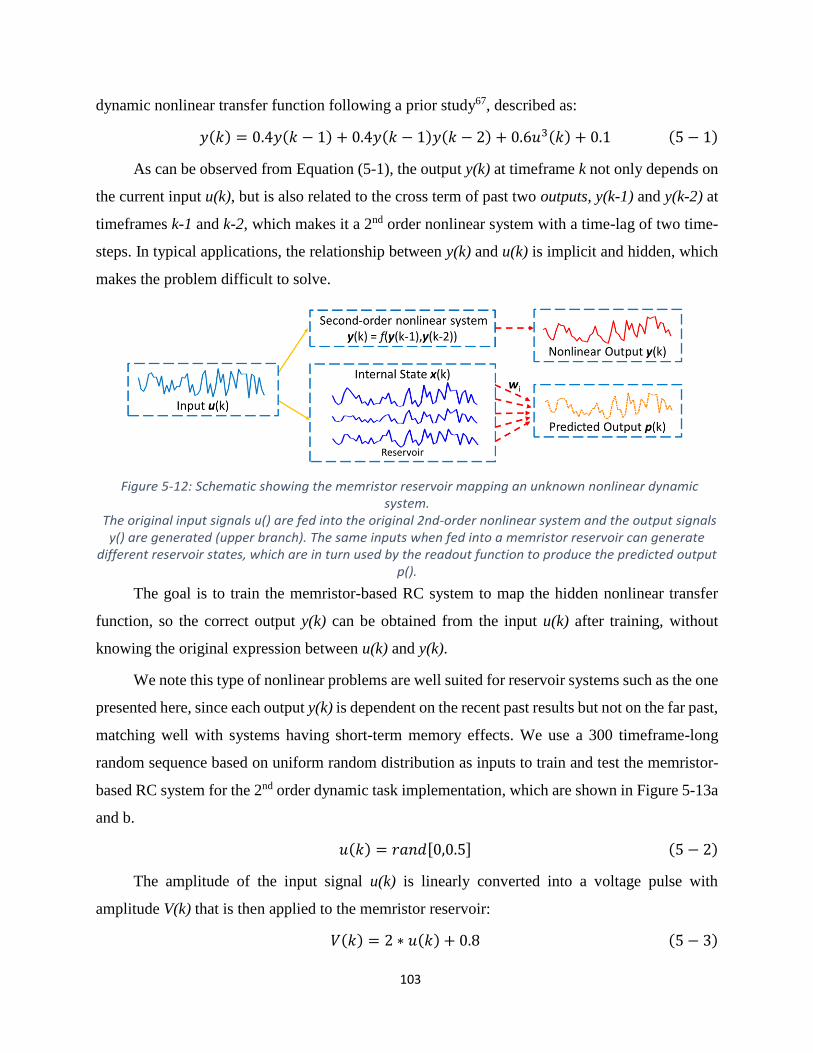
103868
dynamic nonlinear transfer function following a prior study67, described as:
𝑦(𝑘) = 0.4𝑦(𝑘 − 1) + 0.4𝑦(𝑘 − 1)𝑦(𝑘 − 2) + 0.6𝑢3(𝑘) + 0.1 (5 − 1)
As can be observed from Equation (5-1), the output y(k) at timeframe k not only depends on
the current input u(k), but is also related to the cross term of past two outputs, y(k-1) and y(k-2) at
timeframes k-1 and k-2, which makes it a 2nd order nonlinear system with a time-lag of two time-
steps. In typical applications, the relationship between y(k) and u(k) is implicit and hidden, which
makes the problem difficult to solve.
Figure 5-12: Schematic showing the memristor reservoir mapping an unknown nonlinear dynamic system.
The original input signals u() are fed into the original 2nd-order nonlinear system and the output signals y() are generated (upper branch). The same inputs when fed into a memristor reservoir can generate
different reservoir states, which are in turn used by the readout function to produce the predicted output p().
The goal is to train the memristor-based RC system to map the hidden nonlinear transfer
function, so the correct output y(k) can be obtained from the input u(k) after training, without
knowing the original expression between u(k) and y(k).
We note this type of nonlinear problems are well suited for reservoir systems such as the one
presented here, since each output y(k) is dependent on the recent past results but not on the far past,
matching well with systems having short-term memory effects. We use a 300 timeframe-long
random sequence based on uniform random distribution as inputs to train and test the memristor-
based RC system for the 2nd order dynamic task implementation, which are shown in Figure 5-13a
and b.
𝑢(𝑘) = 𝑟𝑎𝑛𝑑[0,0.5] (5 − 2)
The amplitude of the input signal u(k) is linearly converted into a voltage pulse with
amplitude V(k) that is then applied to the memristor reservoir:
𝑉(𝑘) = 2 ∗ 𝑢(𝑘) + 0.8 (5 − 3)

104868
This linear conversion allows the input voltage pulses to fall in the range of 0.8V-1.8V for
memristor stimulation. After collecting the reservoir output, the data is fed into the readout
function. Following a similar approach in a prior study68, we ignore the first 50 initial data points
in the transient period and train the readout function weights 𝑤𝑖 (i=1,…90) using the last 250
points in the training sequence using simple linear regression. The same training procedure is also
applied for the linear network case used for comparison analysis.
The reservoir consists of 90 physical memristor devices chosen from the memristor crossbar
array, and is divided into 10 groups with 9 devices in each group. Input voltage pulse streams with
10 different timeframe widths (1ms, 2ms, 3ms, 4ms, 5ms, 6ms, 8ms, 10ms, 15ms, 20ms) are then
respectively applied to the 10 groups through the test board. We found having 9 devices in each
group improves the reservoir performance due to inherent device variations that help make the
reservoir output more separable, as well as having inputs with different timeframe widths as has
already been discussed in the MNIST case. The readout layer in this case is a 90×1 feedforward
layer, and is used to convert the reservoir output to a single output y(k). A simple linear regression
training algorithm based on batch gradient descent is used to train the readout function.
Suppose the reservoir state is x, which is represented by a vector containing n elements (the
conductance values of the n memristors forming the reservoir). The vector representing the
reservoir state is applied to the readout network.
The cost function is defined as:
𝐽(𝛉) =1
2𝑚∑(𝛉T𝐱(𝑖) − 𝐲(𝑖))
2𝑚
𝑖=1
(5 − 4)
where m is the number of samples, 𝐲(𝑖) is the desired output for input 𝐱(𝑖).
To minimize the cost function, the network is trained using the gradient descent defined as
𝜕𝐽(𝛉)
𝜕𝛉𝑗=
1
𝑚∑(𝛉T𝐱(𝑖) − 𝐲(𝑖))
𝑚
𝑖=1
𝐱𝑗(𝑖)
(5 − 5)
Figure 5-13c shows the experimentally-obtained reconstructed (i.e. predicted) outputs from
the physical memristor RC system after training (red cycles and dashed line), and the theoretical
output (i.e. ground truth) y(k) (blue solid line) from the training sequence, showing the memristor
RC system can correctly solve the dynamic nonlinear problem, with a normalized mean squared

105868
error (NMSE) of 3.61×10⁻³. More importantly, to verify the memristor RC system has indeed
solved the dynamic transfer function, we tested the system using a new, independently generated
random sequence (Figure 5-13b) other than the training sequence. Figure 5-13d shows that the
system is still able to successfully predict the expected dynamic output for the random, untrained
sequence using the same readout function, with a similar NMSE of 3.13×10⁻³.
Figure 5-13: Second order nonlinear system results with memristor reservoir a) Uniform random signals utrain() are used as the training input. b) Theoretical output y() (blue solid
line) vs. experimentally reconstructed output p() from the memristor reservoir computing system (red circles and dashed line), for 100 timeframes from the random training set. c) Another set of uniform
random signals utest() are used to test the RC performance. d) Theoretical output y() (blue solid line) vs. experimentally reconstructed output p() from the memristor RC system (red circles and dashed line), for 100 timeframes from the random untrained test set. The readout function was not re-trained in the test
It is worth mentioning that all the preprocessing and training operations used in the 2nd-order
nonlinear dynamic task are based on linear transformation. As a result, the nonlinear
transformation required by the task has to originate from the intrinsic nonlinear physics of the
memristor device.
To highlight the computing capacity provided by the memristor reservoir, we compared the
RC system performance against a linear network of the same size. We replaced the memristor
reservoir layer with a linear hidden layer, which generates 90 randomly linearly scaled signals of
the original input u(k), with scaling factors:
𝑥(𝑘) = 2 ∗ 𝑟𝑎𝑛𝑑(0,1) ∗ 𝑢(𝑘) (5 − 6)
where the x(k) is scaled and from the original input signal u(k), similar to a current value
through a linear resistor. In this case, there is no longer any nonlinear transform provided by the
reservoir.
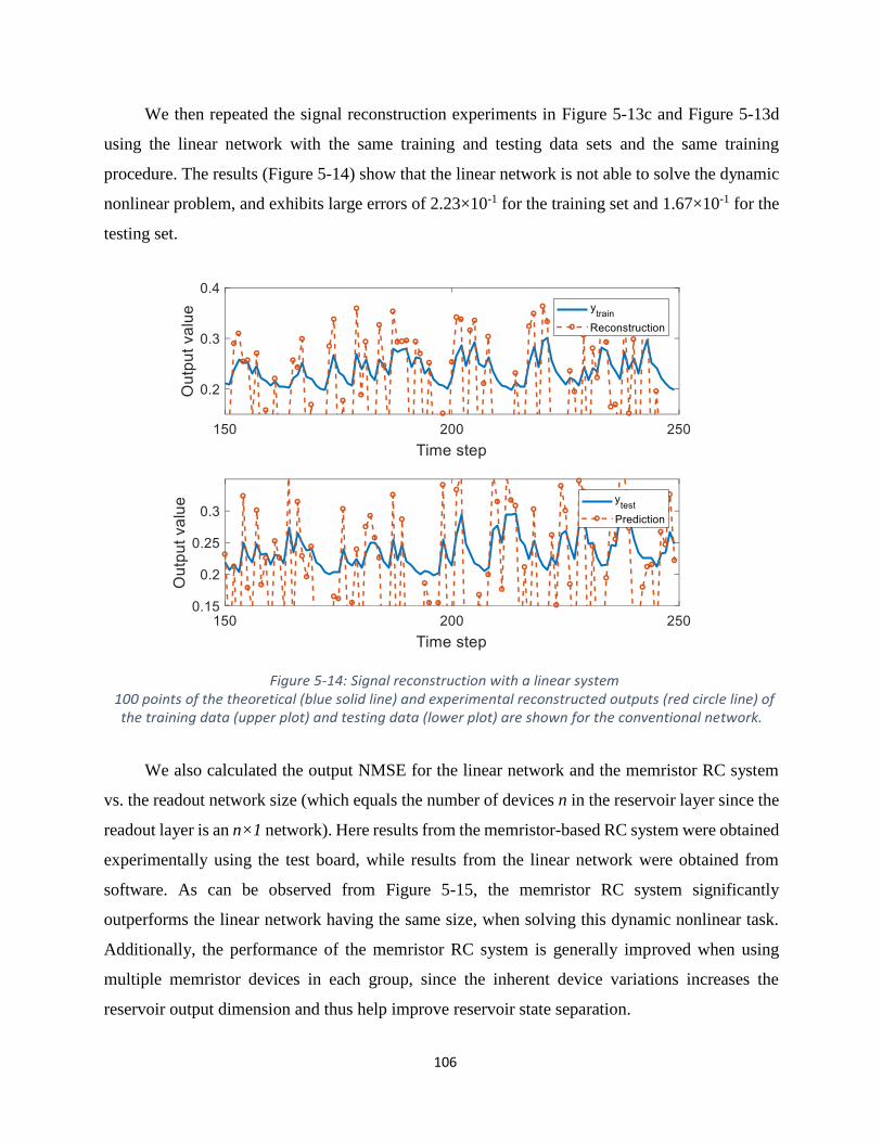
106868
We then repeated the signal reconstruction experiments in Figure 5-13c and Figure 5-13d
using the linear network with the same training and testing data sets and the same training
procedure. The results (Figure 5-14) show that the linear network is not able to solve the dynamic
nonlinear problem, and exhibits large errors of 2.23×10⁻¹ for the training set and 1.67×10⁻¹ for the
testing set.
Figure 5-14: Signal reconstruction with a linear system 100 points of the theoretical (blue solid line) and experimental reconstructed outputs (red circle line) of the training data (upper plot) and testing data (lower plot) are shown for the conventional network.
We also calculated the output NMSE for the linear network and the memristor RC system
vs. the readout network size (which equals the number of devices n in the reservoir layer since the
readout layer is an n×1 network). Here results from the memristor-based RC system were obtained
experimentally using the test board, while results from the linear network were obtained from
software. As can be observed from Figure 5-15, the memristor RC system significantly
outperforms the linear network having the same size, when solving this dynamic nonlinear task.
Additionally, the performance of the memristor RC system is generally improved when using
multiple memristor devices in each group, since the inherent device variations increases the
reservoir output dimension and thus help improve reservoir state separation.

107868
Figure 5-15: Comparison of the NMSE between the memristor RC system and a linear network. The number of devices in each group in the reservoir layer is increased from 1 to 9 in these tests. The
reservoir consists of 10 such groups
5.5 Conclusion
To reduce the training cost needed for temporal data processing, Reservoir Computing is
proposed as a variant of recurrent neural network structure. In an RC system only the readout
function, i.e. the connections from the reservoir to the output, needs to be trained. In this study, we
showed WOx memristors with short-term memory properties can be used to effectively implement
RC systems. We demonstrate experimentally that even a small reservoir consisting of 88 memristor
devices can be used to process real-world problems such as handwritten digit recognition with
performance comparable to those achieved in much larger networks. A similar-sized network is
also used to solve a 2nd-order nonlinear dynamic problem and is able to successfully predict the
expected dynamic output without knowing the form of the transfer function.

108868
Chapter 6 Current and Future Works
In the previous chapters, we discussed examples of implementing neuromorphic computing
systems with WOx memristors, from different device behaviors to fully functional integrated
circuits. We have successfully demonstrated WOx memristor crossbar array-based vector-matrix
multiplication accelerators for conventional machine learning tasks such as perceptron learning
and sparse coding. By using the intrinsic short-term memory dynamics of the device, we can also
implement reservoir computing systems that are efficient at processing temporal information.
In this chapter, we discuss a few current and future studies that aim at solving other tasks
efficiently with the memristor crossbar structures, namely, Hopfield Networks and self-organizing
maps.
6.1 Hopfield Network
A Hopfield Neural Network (HNN) is a form of recurrent artificial neural network
popularized by John Hopfield in 198269. The most important property of a Hopfield network is
that when updated asynchronously, it guarantees to converge to a stable state in a finite number of
steps, which corresponds to an energy local minimum of the network. Since the energy equation
is isomorphic to the Hamiltonian of an Ising model, HNNs can be used to solve NP-hard
problems70.
6.1.1 Properties and Structure
Hopfield network is a type of recurrent neural network that does not contain self-connection
(or have a self-feedback weight of 0)71. Typically, in a Hopfield network, a neuron receives the
outputs of all other neurons as its input, as shown in Figure 6-1.

109868
Figure 6-1: An illustration of a 4-node Hopfield Neural Network
By simply reorganizing the plot, Figure 6-1 can be converted to a graph shown in Figure 6-2.
Figure 6-2: Reorganized Hopfield Neural Network schematic
The weight between neuron i and j (wij) is symmetric.
By using a symmetric matrix with a zero diagonal, we can implement the weights of a
Hopfield network as a n×n matrix.
𝑊 = (
0 𝑤12
𝑤21 0⋯
𝑤1𝑛
𝑤2𝑛
⋮ ⋱ ⋮𝑤𝑛1 𝑤𝑛2 ⋯ 0
) (6 − 1)
The Hopfield network is a dynamical system that can be described as:

110868
𝑢𝑖 = ∑ 𝑤𝑖𝑗𝑣𝑗
𝑛
𝑗
(6 − 2𝑎)
𝑣𝑖 = +1, 𝑖𝑓 𝑢𝑖 ≥ 𝜃𝑖
−1, 𝑜𝑡ℎ𝑒𝑟𝑤𝑖𝑠𝑒 (6 − 2𝑏)
where is the 𝑢𝑖 weighted sum of neuron i, 𝑣𝑖 is the state of neuron i, and 𝜃𝑖 is the threshold
of neuron i.
By asynchronously update the Hopfield network, the network can eventually converge to a
fixed point, which corresponding to the local minima of the following energy function:
𝐸 = −1
2∑ 𝑤𝑖𝑗𝑣𝑖𝑣𝑗
𝑁
𝑖,𝑗
+ ∑ 𝜃𝑖𝑣𝑖
𝑁
𝑖
(6 − 3)
This beneficial property of Hopfield network facilitate to solve large optimization problems.
6.1.2 Memristor Implementation
From Equation (6-2a), we can notice that the key operation of a Hopfield network is also
vector-matrix multiplication. It is thus naturally suitable to be implemented with a memristor
crossbar array, with the weight matrix W programmed into the memristor crossbar. With the high
density and analog switching behavior of memristor array, one should be able to implement large
scale Hopfield network72.

111868
Figure 6-3: Schematic of the Hopfield network implemented by a memristor crossbar array. Image adapted from Reference [72]. Image credit: Dr. Suhas Kumar
In this implementation, the weight of the Hopfield network can be binary or analog
depending on the specific problem to be solved. For example, in the case of solving a unweighted
Max-cut problem73, the weight matrix W is either 0 or -1, which can easily map to low conductance
and high conductance of the memrsitor devices in the array. By iteratively calculating the VMMs
using parallel read and updating the neuron states, the Hopfield network can converge to a fixed
point solution to the NP hard problem.
One advantage of implementing Hopfield network with memristors is that the weight matrix
only need to be programmed once, and most of the operations are performing inference, i.e.
calculating vector-matrix multiplication, which can be done parallelly with very low energy cost.
Compared with other approaches such as quantum annealing (e.g. D-wave), the memristor crossbar
implementation should be able to achieve better efficiency in energy and area.
The major challenge of this approach is the fact that Hopfield network can easily stuck at
local minimums and does not guarantee to find best solution. To solve this issue, an approach of
introducing stochastic noise to improve Hopfield network performance will be studied in future
works.

112868
6.2 Self-Organizing Map
A Self-organizing Map (SOM) is a data visualization technique developed by Professor
Teuvo Kohonen in the early 1980's74. It is an unsupervised learning algorithm that transforms high-
dimensional data onto lower dimensional subspaces where geometric relationships between points
indicate their similarity. The reduction in dimensionality that SOMs provide allows people to
visualize and interpret what would otherwise be, for all intents and purposes, indecipherable data.
Figure 6-4: Illustration of a self-organizing map
6.2.1 Training Algorithm
SOMs generate subspaces with unsupervised learning through a competitive learning
algorithm. Neuron weights are adjusted based on their proximity to "winning" neurons (i.e.
neurons that most closely resemble a sample input). Training over several iterations of input data
sets results in similar neurons grouping together and vice versa.
There are two major steps in the SOM training algorithm
1. Given an input sample from the data set, it will select the best matching unit (BMU),
which is the so-called winning neuron from all the neurons. The besting matching unit
is determined by the Euclidean distance from the neuron and the input
𝑑𝑖𝑠𝑡 = √∑(𝑉𝑖 − 𝑊𝑖)2
𝑑
𝑖=0
(6 − 4)

113868
where V is the input sample and W is the neuron to compare. d is the dimension of the
data.
2. After finding the winning neuron, it will not only update itself, but also adjust the weights
of some nearby neurons within the topological neighborhood. During the training
process, the size 𝜎 of the neighborhood needs to decrease with time and eventually
shrink to 1. Usually the time dependence is an exponential decay:
𝜎(𝑡) = 𝜎0 exp (−𝑡
𝜆) (6 − 5)
The topological neighborhood is then defined with a Gaussian function as:
ℎ(𝑡) = exp (−𝑑𝑖𝑠𝑡2
2𝜎2(𝑡)) (6 − 6)
The weights of the neuron are adjusted as:
𝑊(𝑡 + 1) = 𝑊(𝑡) + 𝜂ℎ(𝑡)(𝑉(𝑡) − 𝑊(𝑡)) (6 − 7)
6.2.2 Memristor Implementation
Unlike the previously discussed Hopfield network implementation that only perform
inference, Self-organizing Map is an online learning algorithm which requires adaptively tuning
the network weights, and can thus be more challenging. However, by taking advantages of the
intrinsic nonlinear characteristics of the memristor devices, the learning processing can potentially
be simplified.
First of all, in SOM, the weight of a neuron usually has multiple dimensions. For example,
if the training data are RGB colors, then we can use three devices at the same column as the weight
of a neuron, namely:
𝑊 = [𝑤𝑅 , 𝑤𝐺 , 𝑤𝐵]𝑇 (6 − 8)
In this case, each neuron requires three rows to implement. To implement an 8×8 SOM, we
need a memristor array of 3×64, which is a fairly asymmetric size to fit in a square array. By
folding the memristor array into multiple rows and use time multiplexing, we can instead use a
12×16 subarray from a 16×16 array.

114868
Figure 6-5: Folding the memristor array to fit in a square array. By storing the weight in a folded matrix and read each three-row batch with time multiplexing, we can
transform a 3×64 weight matrix into a 12×16 one.
The key steps in the training algorithm are to find the best matching unit (i.e. the winning
neuron) and to perform nonlinear weight update at different distances.
Finding the BMU is essentially calculating the minimum of the Euclidean distance, which is
very similar to the winner-take-all approach discussed in Chapter 3. By using memristor crossbar
structure, we can easily convert the calculation of the Euclidean distance to the comparison of the
dot-product value, reducing the computation complexity. To avoid the lack of normalization issue
discussed in section 3.3.2, we can use some correction method introduced in the reference75 to
improve the accuracy in calculating Euclidean distance.
Another challenge is the implementation of the gaussian function to calculate the topological
neighborhood, which requires significant pre-processing in the training process. However, since
the memristor device exhibits an exponentially nonlinear weight update function vs the applied
voltage18, we can obtain the desired exponentially varying weight changes in Equation (6-7) by
simply using a linear decaying programming voltage, with further distance from the winning
neuron in the 2-D map corresponding to lower programming voltage. With this approach, the most
computational expensive part in training can be simplified by device intrinsic physics.
Further works will focus on the experimental implementation of the SOM on a 12×16
memristor that aims at clustering different RGB colors.

115868
References
1. Moore, G. E. Cramming More Components onto Integrated Circuits. Electronics 38, 114–
117 (1965).
2. Waldrop, M. M. The chips are down for Moore’s law. Nature 530, 144–147 (2016).
3. Hutchby, J. A., Bourianoff, G. I., Zhirnov, V. V. & Brewer, J. E. Extending the road
beyond CMOS. IEEE Circuits Devices Mag. 18, 28–41 (2002).
4. Khan, H. N., Hounshell, D. A. & Fuchs, E. R. H. Science and research policy at the end of
Moore’s law. Nat. Electron. 1, 14–21 (2018).
5. Von Neumann, J. First Draft of a Report on the EDVAC. IEEE Ann. Hist. Comput. 27–75
(1993).
6. Merkle, R. C. Energy Limits to the Computational Power of the Human Brain The Brain
as a Computer. Foresight Updat. 6–8 (1989).
7. Sarpeshkar, R. in Ultra Low Power Bioelectronics: Fundamentals, Biomedical
Applications, and Bio-Inspired Systems 697–752 (Cambridge University Press, 2010).
8. Mead, C. Neuromorphic electronic systems. Proc. IEEE 78, 1629–1636 (1990).
9. Sarpeshkar, R. Analog versus digital: extrapolating from electronics to neurobiology.
Neural Comput. 10, 1601–38 (1998).
10. Chua, L. Memristor-The missing circuit element. IEEE Trans. Circuit Theory 18, 507–519
(1971).
11. Jo, S. H., Kim, K.-H. & Lu, W. High-density crossbar arrays based on a Si memristive
system. Nano Lett. 9, 870–4 (2009).
12. Strukov, D. B., Snider, G. S., Stewart, D. R. & Williams, R. S. The missing memristor
found. Nature 453, 80–83 (2008).
13. Pershin, Y. V. & Di Ventra, M. Neuromorphic, digital, and quantum computation with
memory circuit elements. Proc. IEEE 100, 2071–2080 (2012).
14. Waser, R. & Aono, M. Nanoionics-based resistive switching memories. Nat. Mater. 6,
833–840 (2007).

116868
15. Park, G.-S. et al. In situ observation of filamentary conducting channels in an asymmetric
Ta2O5−x/TaO2−x bilayer structure. Nat. Commun. 4, 2382 (2013).
16. Yang, Y. et al. Observation of conducting filament growth in nanoscale resistive
memories. Nat. Commun. 3, 732 (2012).
17. Chang, T., Jo, S.-H. H. & Lu, W. Short-term memory to long-term memory transition in a
nanoscale memristor. ACS Nano 5, 7669–7676 (2011).
18. Chang, T. et al. Synaptic behaviors and modeling of a metal oxide memristive device.
Appl. Phys. A 102, 857–863 (2011).
19. Yang, J. J. et al. Memristive switching mechanism for metal/oxide/metal nanodevices.
Nat. Nanotech. 3, 429–433 (2008).
20. Lee, M.-J. et al. A fast, high-endurance and scalable non-volatile memory device made
from asymmetric Ta2O5−x/TaO2−x bilayer structures. Nat. Mater. 10, 625–630 (2011).
21. Jo, S. H. et al. Nanoscale Memristor Device as Synapse in Neuromorphic Systems. Nano
Lett. 10, 1297–1301 (2010).
22. Prezioso, M. et al. Training and operation of an integrated neuromorphic network based
on metal-oxide memristors. Nature 521, 61–64 (2015).
23. Yao, P. et al. Face classification using electronic synapses. Nat. Commun. 8, 15199
(2017).
24. Bayat, F. M. et al. Implementation of multilayer perceptron network with highly uniform
passive memristive crossbar circuits. Nat. Commun. 9, 2331 (2018).
25. Li, C. et al. Efficient and self-adaptive in-situ learning in multilayer memristor neural
networks. Nat. Commun. 9, 2385 (2018).
26. Li, C. et al. Analogue signal and image processing with large memristor crossbars. Nat.
Electron. 1, (2017).
27. Gao, L., Chen, P.-Y. & Yu, S. Demonstration of Convolution Kernel Operation on
Resistive Cross-Point Array. IEEE Electron Device Lett. 37, 870–873 (2016).
28. Sheridan, P. M. et al. Sparse coding with memristor networks. Nat. Nanotech. 12, 784–
789 (2017).
29. Du, C. et al. Reservoir computing using dynamic memristors for temporal information
processing. Nat. Commun. 8, 2204 (2017).
30. Choi, S., Shin, J. H., Lee, J., Sheridan, P. & Lu, W. D. Experimental Demonstration of

117868
Feature Extraction and Dimensionality Reduction Using Memristor Networks. Nano Lett.
17, 3113–3118 (2017).
31. Jeong, D. S. & Hwang, C. S. Nonvolatile Memory Materials for Neuromorphic Intelligent
Machines. Adv. Mater. 1704729, 1–27 (2018).
32. Yang, J. J., Strukov, D. B. & Stewart, D. R. Memristive devices for computing. Nat.
Nanotech. 8, 13–24 (2013).
33. Zidan, M. A., Strachan, J. P. & Lu, W. D. The future of electronics based on memristive
systems. Nat. Electron. 1, 22–29 (2018).
34. Cai, F. & Lu, W. D. Feature extraction and analysis using memristor networks. in 2018
IEEE International Symposium on Circuits and Systems (ISCAS) 1–4 (2018).
doi:10.1109/ISCAS.2018.8351831
35. Olshausen, B. A. & Field, D. J. Sparse coding with an overcomplete basis set: A strategy
employed by V1? Vision Res. 37, 3311–3325 (1997).
36. Vinje, W. E. Sparse Coding and Decorrelation in Primary Visual Cortex During Natural
Vision. Science (80-. ). 287, 1273–1276 (2000).
37. Wright, J. et al. Sparse Representation for Computer Vision and Pattern Recognition.
Proc. IEEE 98, 1031–1044 (2010).
38. Olshausen, B. A. & Field, D. J. Emergence of simple-cell receptive field properties by
learning a sparse code for natural images. Nature 381, 607–609 (1996).
39. Zylberberg, J., Murphy, J. T. & DeWeese, M. R. A sparse coding model with synaptically
local plasticity and spiking neurons can account for the diverse shapes of V1 simple cell
receptive fields. PLoS Comput. Biol. 7, (2011).
40. Rozell, C. J., Johnson, D. H., Baraniuk, R. G. & Olshausen, B. A. Sparse coding via
thresholding and local competition in neural circuits. Neural Comput. 20, 2526–63 (2008).
41. Hubel, D. H. & Wiesel, T. N. Receptive fields, binocular interaction and functional
architecture in the cat’s visual cortex. J. Physiol. 160, 106–154.2 (1962).
42. Hu, M. et al. Memristor-Based Analog Computation and Neural Network Classification
with a Dot Product Engine. Adv. Mater. 1705914, 1–10 (2018).
43. Sheridan, P. M., Du, C. & Lu, W. D. Feature Extraction Using Memristor Networks. IEEE
Trans. Neural Networks Learn. Syst. 27, 2327–2336 (2016).
44. Mairal, J. Sparse Modeling for Image and Vision Processing. Found. Trends® Comput.

118868
Graph. Vis. 8, 85–283 (2014).
45. Rubinstein, R., Bruckstein, A. M. & Elad, M. Dictionaries for sparse representation
modeling. Proc. IEEE 98, 1045–1057 (2010).
46. Oja, E. Simplified neuron model as a principal component analyzer. J. Math. Biol. 15,
267–273 (1982).
47. Ma, W. et al. Device nonideality effects on image reconstruction using memristor arrays.
in 2016 IEEE International Electron Devices Meeting (IEDM) 16.7.1-16.7.4 (IEEE,
2016).
48. Cai, F. & Lu, W. D. Epsilon-greedy strategy for online dictionary learning with realistic
memristor array constraints. in 2017 IEEE/ACM International Symposium on Nanoscale
Architectures (NANOARCH) 19–20 (IEEE, 2017).
49. Sutton, R. S. & Barto, A. G. Introduction to reinforcement learning. 135, (MIT press
Cambridge, 1998).
50. Xia, Q. et al. Memristor-CMOS hybrid integrated circuits for reconfigurable logic. Nano
Lett. 9, 3640–3645 (2009).
51. Kim, K.-H. et al. A Functional Hybrid Memristor Crossbar-Array/CMOS System for Data
Storage and Neuromorphic Applications. Nano Lett. 12, 389–395 (2012).
52. Lever, J., Krzywinski, M. & Altman, N. Points of Significance: Principal component
analysis. Nat. Methods 14, 641–642 (2017).
53. Choi, S. et al. SiGe epitaxial memory for neuromorphic computing with reproducible high
performance based on engineered dislocations. Nat. Mater. 17, 335–340 (2018).
54. Taur, Y. & Ning, T. H. Fundamentals of Modern VLSI Devices. (Cambridge University
Press, 2009). doi:10.1017/CBO9781139195065
55. Murmann, B. ADC performance survey 1997-2018.
http://web.stanford.edu/~murmann/adcsurvey.html (2018).
56. Du, C., Ma, W., Chang, T., Sheridan, P. & Lu, W. D. Biorealistic Implementation of
Synaptic Functions with Oxide Memristors through Internal Ionic Dynamics. Adv. Funct.
Mater. 25, 4290–4299 (2015).
57. Ohno, T. et al. Short-term plasticity and long-term potentiation mimicked in single
inorganic synapses. Nat. Mater. 10, 591–595 (2011).
58. Verstraeten, D. et al. An experimental unification of reservoir computing methods. Neural

119868
Networks 20, 391–403 (2007).
59. Appeltant, L. et al. Information processing using a single dynamical node as complex
system. Nat. Commun. 2, 468 (2011).
60. Maass, W., Natschlager, T. & Markram, H. Real-time computing without stable states: a
new framework for neural computation based on perturbations. Neural Comput 14, 2531–
2560 (2002).
61. Lukoševičius, M. & Jaeger, H. Reservoir computing approaches to recurrent neural
network training. Comput. Sci. Rev. 3, 127–149 (2009).
62. Wang, Z. et al. Memristors with diffusive dynamics as synaptic emulators for
neuromorphic computing. Nat. Mater. 1, 101–108 (2016).
63. Burger, J. & Teuscher, C. Variation-tolerant Computing with Memristive Reservoirs. in
2013 IEEE/ACM International Symposium on Nanoscale Architectures (NANOARCH) 1–
6 (IEEE, 2013).
64. LeCun, Y., Cortes, C. & Burges, C. J. C. The MNIST database of handwritten digits.
(1998).
65. LeCun, Y., Bottou, L., Bengio, Y. & Haffner, P. Gradient-based learning applied to
document recognition. Proc. IEEE 86, 2278–2324 (1998).
66. Khalil, H. K. Noninear Systems. Prentice-Hall, New Jersey 2, 1–5 (1996).
67. Atiya, A. F. & Parlos, A. G. New results on recurrent network training: unifying the
algorithms and accelerating convergence. IEEE Trans. Neural Networks 11, 697–709
(2000).
68. Jaeger, H. Harnessing Nonlinearity: Predicting Chaotic Systems and Saving Energy in
Wireless Communication. Science (80-. ). 304, 78–80 (2004).
69. Hopfield, J. J. Computational Abilities. Biophysics (Oxf). 79, 2554–2558 (1982).
70. Lucas, A. Ising formulations of many NP problems. 2, 1–15 (2013).
71. Hopfield, J. J. Neurons with graded response have collective computational properties like
those of two-state neurons. Proc. Natl. Acad. Sci. 81, 3088–3092 (1984).
72. Kumar, S., Strachan, J. P. & Williams, R. S. Chaotic dynamics in nanoscale NbO 2 Mott
memristors for analogue computing. Nature 548, 318–321 (2017).
73. Karp, R. M. in 50 Years of Integer Programming 1958-2008 219–241 (Springer Berlin
Heidelberg, 2010). doi:10.1007/978-3-540-68279-0_8

120868
74. Kohonen, T. Self-organized formation of topologically correct feature maps. Biol. Cybern.
43, 59–69 (1982).
75. Jeong, Y., Lee, J., Moon, J., Shin, J. H. & Lu, W. D. K -means Data Clustering with
Memristor Networks. Nano Lett. 18, 4447–4453 (2018).