new and emerging technologies - smta · pdf filetrying for a terahertz transistor ... in...
TRANSCRIPT

2/19/2014
1
Confidential/Competition Sensitive Daniel F. Baldwin, Ph.D.© ENGENT. INC. 1/21/14
New and Emerging Technologies in Electronics
Daniel F. Baldwin, Ph.D.PresidentEngent, Inc.3140 Northwoods ParkwaySuite 300ANorcross Georgia [email protected]
Confidential/Competition Sensitive Daniel F. Baldwin, Ph.D.© ENGENT. INC. 1/21/14
Overview
The Next Paradigm
Snap Shot of Emerging Technologies
Semiconductor Technology
Automotive Electronics
Biomedical Electronics
Assembly Roadmap Highlights

2/19/2014
2
Confidential/Competition Sensitive Daniel F. Baldwin, Ph.D.© ENGENT. INC. 1/21/14
1900
Electromechanical Relay Transistor Integrated Circuit
Vacuum Tube
10-8
10-2
104
108
10-4
102
100
106
1010
Calculations Per Second Per $1000
1910 1920 1930 1940 1950 1960 1970 1980 1990 2000
WY
93.2
80be
s-pa
radi
gm
Moore’s Law – The Fifth Paradigm
What’s Next? 3D versus 2D device structures Nanotechnology
Molecular/optical/quantum computing
Smart/Intelligent ElectronicsSource: Wikipedia
Prismark
Adapted from Kurzweil
Confidential/Competition Sensitive Daniel F. Baldwin, Ph.D.© ENGENT. INC. 1/21/14
Beyond Moore’s Law
Nanowire Computing Made Practical IBM has developed a process for making speedier and more energy-efficient chips. One of the leading candidates for a technology that
could make computers smaller and more powerful is based on transistors made from semiconducting nanowires. Read More
Nanotube Ink Printable carbon nanotube patterns could find uses in flexible displays and RFID tags.
Small, Cheaper Flash Memory Freescale Semiconductor is using nanoscale materials to halve the size of flash memory and make it much less expensive.
Trying for a Terahertz Transistor A new transistor design aims to smash speed records.
A New Spin on Computing Researchers have found a material that could allow the use of spintronics to make more-powerful computers.
A Universal Chip for Cell Phones A single chip for wireless devices that's multifunctional, more energy efficient, and space saving is in the works.
Holograms Break Storage Record New technology has almost twice the storage density of a magnetic hard drive.
Carbon Nanotube Computers IBM researchers have made an important breakthrough: arranging nanotube transistors for complex circuits.
A Breakthrough in Nanotube Transistors High-current transistors made from perfectly aligned carbon nanotubes show promise for use in flexible and high-speed nanoelectronics.
Bringing Light to Silicon Intel has announced a new silicon laser that can transfer data on a beam of light--and could make computers many times faster.
A Laser Technique Could Improve Electronics This novel process might lead to purer silicon -- and faster chips.
How to Burn a Three Terabyte CD A new nano-optical device can focus laser light tighter than traditional optics, which could lead to higher-density data storage.
Three-Dimensional Transistors from Lab to Fab Processors that use the “tri-gate” transistors have been demonstrated in working systems, and the company will begin volume production.
Nanowire Transistors Faster than Silicon Advances in nanowires show they can be fast enough to use as ultrasmall transistors in cheap, high-performance electronics.
Source: Technology Review

2/19/2014
3
Confidential/Competition Sensitive Daniel F. Baldwin, Ph.D.© ENGENT. INC. 1/21/14
Silicon Fabrication Technology Nodes
Source: Intel
Confidential/Competition Sensitive Daniel F. Baldwin, Ph.D.© ENGENT. INC. 1/21/14
Silicon Fabrication Technology Nodes
Source: Intel

2/19/2014
4
Confidential/Competition Sensitive Daniel F. Baldwin, Ph.D.© ENGENT. INC. 1/21/14
Silicon on Insulator, Tri-Gates, and FinFETs
SOI uses a layered silicon-insulator-silicon substrate in place of conventional silicon substrates in semiconductor manufacturing, to reduce parasitic device capacitance, thereby improving performance.
Tri-Gate transistors employ a single gate stacked on top of two vertical gates allowing for essentially three times the surface area for electrons to travel. Intel reports tri-gate transistors reduce leakage and consume far less power than current transistors. This allows up to 37% higher speed, or a power consumption at under 50% of the previous type of transistors used by Intel.
FinFETs are nonplanar, double-gate transistor built on an SOI substrate. The distinguishing characteristic of the FinFET is that the conducting channel is wrapped by a thin silicon "fin", which forms the body of the device. The thickness of the fin (measured in the direction from source to drain) determines the effective channel length of the device.
Source: IBM, Wikipedia
FinFET
Fin on Oxide
Tri-Gate Transistors
Confidential/Competition Sensitive Daniel F. Baldwin, Ph.D.© ENGENT. INC. 1/21/14
Vacuum Dielectrics
A main source of the signal lag is not so much the metal interconnects themselves but rather the insulation between the wires. So the question is, what can you put between those wires to prevent the signal from leaking?
Vacuum is the best insulator known.
IBM’s Air-gap technology carves nanoscale holes into the insulation between a chip’s copper wires, as seen in this electron micrograph.
Source: IEEE Spectrum

2/19/2014
5
Confidential/Competition Sensitive Daniel F. Baldwin, Ph.D.© ENGENT. INC. 1/21/14
Semiconductor Nanowires
New strategies, including the use of novel materials and one-dimensional (1D) device concepts, innovative device architectures, and smart integration schemes are being explored and are crucial to extending current capabilities the post CMOS era.
Functional nanostructures, particularly one-dimensional semiconductor nanowires have been demonstrated.
Source: IBM
Demonstration of first vertical surround-gate Si-nanowire transistor, see image at right. A surround-gate allows the optimal electrostatic control over the channel
Confidential/Competition Sensitive Daniel F. Baldwin, Ph.D.© ENGENT. INC. 1/21/14
Silicon Nanowire MOSFETs
IBM researchers havd developed a silicon nanowire (SiNW)-based MOSFET fabrication process that produced gate-all-around (GAA) SiNW devices at sizes compatible with the scaling needs of 10nm CMOS technology.
They built a range of GAA SiNW MOSFETs, some of which featured an incredible 30nm SiNW pitch (the spacing between adjacent nanowires) with a gate pitch of 60nm. Devices with a 90nm gate pitch demonstrated the highest performance ever reported for a SiNW device at a gate pitch below 100nm—peak/saturation current of 400/976µA/µm, respectively, at 1 V.
Although this work focused on NFETs, the researchers say the same fabrication techniques can be used to produce PFETs as well, opening the door to a potential ultra-dense, high-performance CMOS technology.
Source: Solid State Technology
cross section of a completed device through a gate, illustrating the spacer, epitaxial source/drain and contacts

2/19/2014
6
Confidential/Competition Sensitive Daniel F. Baldwin, Ph.D.© ENGENT. INC. 1/21/14
Monolithic 3D Chip
An alternative to scaling is to expand vertically. Although 3D circuits often are made by stacking separate chips and connecting them with through-silicon vias (TSVs), some TSVs also have major disadvantages, including relatively large dimensions, parasitic capacitances and thermal mismatch issues.
Researchers from Taiwan’s National Nano Device Laboratories avoided the use of TSVs by fabricating a monolithic sub-50nm 3D chip, which integrates high-speed logic and nonvolatile and SRAM memories.
They built it from ultrathin-body MOSFETs isolated by 300nm-thick interlayer dielectric layers. To build the device layers, the researchers deposited amorphous silicon and crystallized it with laser pulses. They then used a novel low-temperature chemical mechanical planarization (CMP) technique to thin and planarize the silicon, enabling the fabrication of ultrathin, ultraflat devices.
Source: Solid State Technology
Confidential/Competition Sensitive Daniel F. Baldwin, Ph.D.© ENGENT. INC. 1/21/14
Graphene Seminconductors
Researchers have discovered a new way to switch current on and off in graphene, pointing the way to the possibility of molecule-size memory.
Graphene is a 1-atom-thick carbon molecule in which electrons flow 100 times as fast as they do in silicon. In theory, a graphene transistor would be 100 times as fast as the same device made of silicon. One challenge, though, is that graphene is so conductive that it’s hard to stop current from flowing, and such on-off switching is necessary for any sort of transistor.
It is believed that with graphene, a device could, in principle, be scaled down to a 1-nanometer-by-1-nanometer size.
The switching is not fast enough to be used in a logic circuit, and researchers have not yet shown that it will work for the millions of cycles a memory device would require.
Graphene is presently one of the most expensivematerials on Earth. It is the strongest substance known to man and can be made into a conformalsurface.
Source: IEEE SpectrumWikipedia

2/19/2014
7
Confidential/Competition Sensitive Daniel F. Baldwin, Ph.D.© ENGENT. INC. 1/21/14
Memristor
Fourth basic element in integrated circuits that could make it possible to develop computers that turn on and off like an electric light.
Short for memory resistor
A class of passive two-terminal circuit elements that maintain a functional relationship between the time integrals of current and voltage.
Results in resistance varying according to the device's memristance function.
Specifically engineered memristors provide controllable resistance useful for switching current.
Could make it possible for memories that retain information even after the power is off, so there's no wait for the system to boot up after turning the computer on.
May even be possible to create systems with some of the pattern-matching abilities of the human brain.
wires are 50 nm - about 150 atoms - wide
Source: HP
Confidential/Competition Sensitive Daniel F. Baldwin, Ph.D.© ENGENT. INC. 1/21/14
3D Integration Roadmap
Source: iNEMI
2/19/2014
8
Confidential/Competition Sensitive Daniel F. Baldwin, Ph.D.© ENGENT. INC. 1/21/14
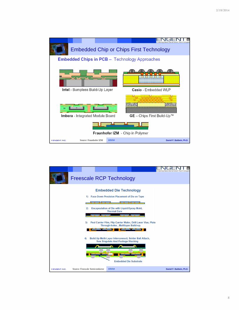
Embedded Chip or Chips First Technology
Source: Fraunhofer IZM
Confidential/Competition Sensitive Daniel F. Baldwin, Ph.D.© ENGENT. INC. 1/21/14
Freescale RCP Technology
Source: Freescale Semiconductor

2/19/2014
9
Confidential/Competition Sensitive Daniel F. Baldwin, Ph.D.© ENGENT. INC. 1/21/14
3D Wafer Level Integration Concept
3D integration represents a system-level integration scheme wherein multiple layers of planar devices are stacked and interconnected using through-wafer vias in the Z direction.
Source: RIT & IBM
Confidential/Competition Sensitive Daniel F. Baldwin, Ph.D.© ENGENT. INC. 1/21/14
Technologies Enabling 3D Integration
Through Silicon Via – active wafer & interposers
Two side wafer level Processes RDL and MicroBumping
Embedded Components (active & passive)
Wafer Thinning & Handling
Wafer to Wafer Bonding
Die to Wafer Bonding
Microbump assembly
Design Tools
Microfluidics Cooling
Assembly of TSV die
Test of TSV Die
Source: iNEMI
2/19/2014
10
Confidential/Competition Sensitive Daniel F. Baldwin, Ph.D.© ENGENT. INC. 1/21/14
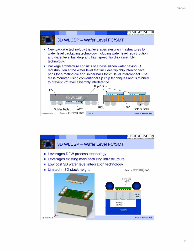
3D WLCSP – Wafer Level FC/SMT
New package technology that leverages existing infrastructures for wafer level packaging technology including wafer level redistribution and wafer level ball drop and high speed flip chip assembly technology.
Package architecture consists of a base silicon wafer having IO redistribution at the wafer level that includes flip chip interconnect pads for a mating die and solder balls for 2nd level interconnect. The die is mounted using conventional flip chip techniques and is thinned to prevent 2nd level assembly interference.
Flip Chips
TSVRDLSolder Balls Solder BallsACT
PA
Source: ENGENT, INC.
Confidential/Competition Sensitive Daniel F. Baldwin, Ph.D.© ENGENT. INC. 1/21/14
Driver ChipASIC
Cap Die
MEMSDie
Through Die Vias
3D WLCSP – Wafer Level FC/SMT
Leverages D2W process technology
Leverages existing manufacturing infrastructure
Low cost 3D wafer level integration technology
Limited in 3D stack height Source: ENGENT, INC.
2/19/2014
11
Confidential/Competition Sensitive Daniel F. Baldwin, Ph.D.© ENGENT. INC. 1/21/14
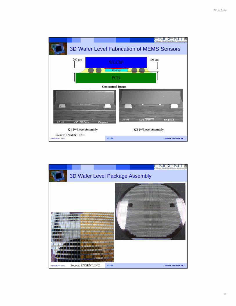
3D Wafer Level Fabrication of MEMS Sensors
Q1 2nd Level Assembly Q3 2nd Level Assembly
Conceptual Image
Source: ENGENT, INC.
Confidential/Competition Sensitive Daniel F. Baldwin, Ph.D.© ENGENT. INC. 1/21/14
3D Wafer Level Package Assembly
Source: ENGENT, INC.
2/19/2014
12
Confidential/Competition Sensitive Daniel F. Baldwin, Ph.D.© ENGENT. INC. 1/21/14
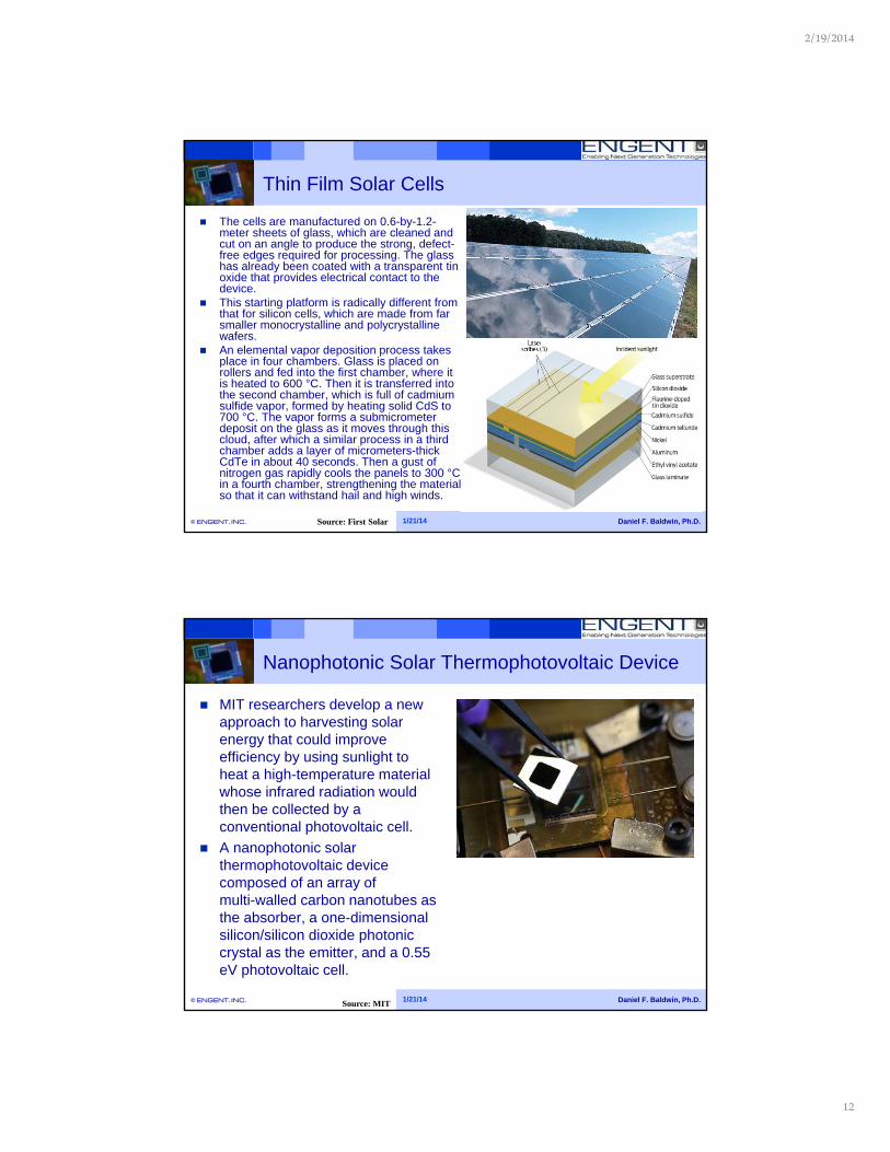
Thin Film Solar Cells
The cells are manufactured on 0.6-by-1.2-meter sheets of glass, which are cleaned and cut on an angle to produce the strong, defect-free edges required for processing. The glass has already been coated with a transparent tin oxide that provides electrical contact to the device.
This starting platform is radically different from that for silicon cells, which are made from far smaller monocrystalline and polycrystalline wafers.
An elemental vapor deposition process takes place in four chambers. Glass is placed on rollers and fed into the first chamber, where it is heated to 600 °C. Then it is transferred into the second chamber, which is full of cadmium sulfide vapor, formed by heating solid CdS to 700 °C. The vapor forms a submicrometer deposit on the glass as it moves through this cloud, after which a similar process in a third chamber adds a layer of micrometers-thick CdTe in about 40 seconds. Then a gust of nitrogen gas rapidly cools the panels to 300 °C in a fourth chamber, strengthening the material so that it can withstand hail and high winds.
Source: First Solar
Confidential/Competition Sensitive Daniel F. Baldwin, Ph.D.© ENGENT. INC. 1/21/14
Nanophotonic Solar Thermophotovoltaic Device
MIT researchers develop a new approach to harvesting solar energy that could improve efficiency by using sunlight to heat a high-temperature material whose infrared radiation would then be collected by a conventional photovoltaic cell.
A nanophotonic solar thermophotovoltaic device composed of an array of multi-walled carbon nanotubes as the absorber, a one-dimensional silicon/silicon dioxide photonic crystal as the emitter, and a 0.55 eV photovoltaic cell.
Source: MIT
2/19/2014
13
Confidential/Competition Sensitive Daniel F. Baldwin, Ph.D.© ENGENT. INC. 1/21/14
Organic Electronics
Organic semiconductors are strong candidates for creating flexible, full-color displays and circuits on plastic.
Using organic light-emitting devices (OLEDs), organic full-color displays may eventually replace liquid-crystal displays (LCDs) for use with laptop and even desktop computers. Such displays can be deposited on flexible plastic foils
Currently, efficiencies of the best doped polymer and molecular OLEDs exceed that of incandescent light bulbs. Efficiencies of 20 lumens per watt have been reported for yellow-green-emitting polymer devices, and 40 lm/W attained for phosphorescent molecular OLEDs, compared to less than 20 lm/W for a typical incandescent light bulb. It is reasonable to predict that soon, efficiencies of 80 lm/W—a value comparable to that of fluorescent room lighting—will be achieved using phosphorescent OLEDs.
It is reasonable to assume that within 10 years, the square footage of organic circuitry might exceed that of silicon electronics
Source: IEEESpectrum
An organic passive-matrix display on a substrate of PET, a lightweight plastic, will bend around a diameter of less than a centimeter.
Confidential/Competition Sensitive Daniel F. Baldwin, Ph.D.© ENGENT. INC. 1/21/14
Eye Electronics
Contact lens made in the secretive Google X labs is designed to help diabetics by transmitting a feed of the glucose levels in their tears to a nearby receiver
Swiss company Sensimed, has been tested on people. Several hospitals are trialing it to track pressure levels in a person’s eye over a 24-hour period to help manage glaucoma
Source: MIT Technology Review
2/19/2014
14
Confidential/Competition Sensitive Daniel F. Baldwin, Ph.D.© ENGENT. INC. 1/21/14
Bendable Microchips
IMEC has developed a way to put integrated circuits into flexible and stretchable materials without impairing the microchip’s functionality. The technique could lead to more sophisticated biomedical implants or electronics embedded in clothing.
Flexible electronics usually consist of circuits made up of individual components embedded in an elastic material and connected together by stretchable interconnects. This approach can create basic circuits capable of, for example, simple sensing functions.
This “thinned-down” flexible microprocessor is connected via stretchable copper interconnects, all using conventional materials.
Source: MIT Technology Review
Confidential/Competition Sensitive Daniel F. Baldwin, Ph.D.© ENGENT. INC. 1/21/14
Electronic Skin Emits Light
A sheet of thin plastic that emits light with an intensity that precisely reflects the amount of pressure applied to its surface hints at a new breed of flexible computer interface. Its creators say future iterations of the interface could be used for robotics, car dashboards, mobile displays, or even “interactive wallpaper.”
Prof. Javey’s group at UC Berkeley has developed processes that draw heavily on traditional silicon manufacturing techniques to uniformly and reliably integrate various organic and inorganic components on top of plastic.
Fully fabricated piece of “electronic skin.” Each pixel emits light in response to applied pressure.

2/19/2014
15
Confidential/Competition Sensitive Daniel F. Baldwin, Ph.D.© ENGENT. INC. 1/21/14
Organic Transistor
A transistor that emits light and is made from organic materials could lead to cheaper digital displays and fast-switching light sources on computer chips, according to the researchers.
The new organic light-emitting transistor (OLET) is much more efficient than previous designs. It has an external quantum efficiency of 5% (0.6% for previous designs), compared to an OLED based on the same material of 2%.
A transistor-based light source would switch much faster than a diode, and more easily integrated onto ICs providing faster data transmission across chips than copper wire.
The unique three-layer structure leads to higher efficiency. Current flows horizontally through the top and bottom layers—one carrying electrons and the other holes—while carriers that wander into the central layer recombine and emit photons.
Source: IEEE Spectrum
Confidential/Competition Sensitive Daniel F. Baldwin, Ph.D.© ENGENT. INC. 1/21/14
This microprocessor is made from organic materials. It is puny compared to most silicon processors, but is flexible and cheap
Fabricated on 0.6 mm Flexible Film
4000 Organic Transistors
Collaboration between: IMEC in Leuven, Belgium
TNO research organization, Netherlands
Polymer Vision display company,Netherlands
Can run only one 16 instruction program. Commands are hardcoded on 2nd foil etched with plastic circuits. Processor calculates running average of an incomingsignal, a simple operation for conventionalmicroprocessors. The chip runs at six hertz-on order of a million times slower than a modern desktop machine-and can only process information in 8 bits, compared todays128 bits processors
Plastic Computer Processor
Source: Technology Review, IMEC
~ 2cm
2/19/2014
16
Confidential/Competition Sensitive Daniel F. Baldwin, Ph.D.© ENGENT. INC. 1/21/14
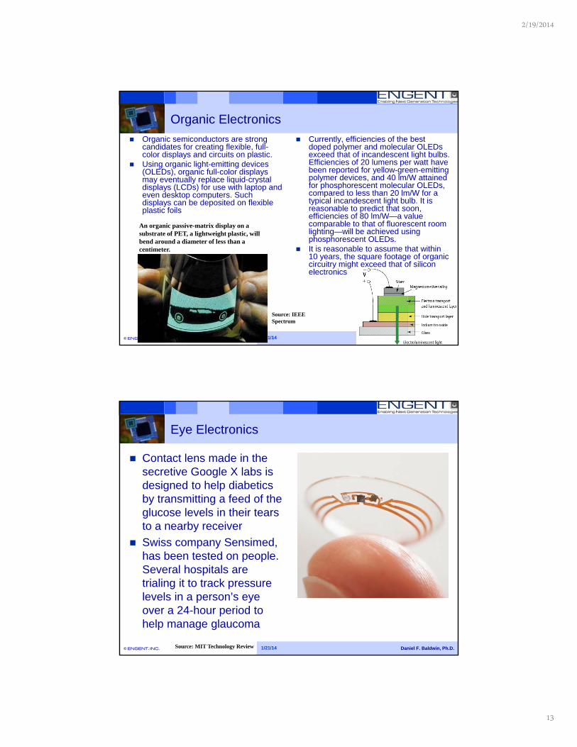
Printed Displays
Source: E Ink
-
+
Kindle ®Wireless Reading Device
Confidential/Competition Sensitive Daniel F. Baldwin, Ph.D.© ENGENT. INC. 1/21/14
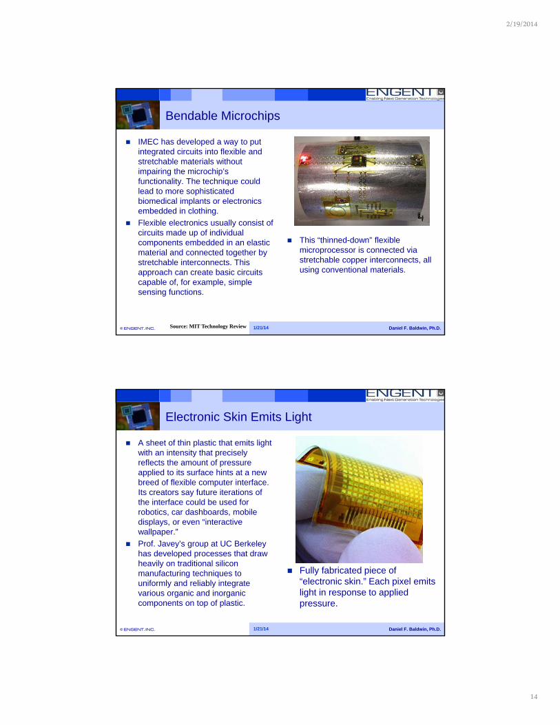
Automotive Electronics
Sensor Rich Environment Electro Mechanical Replacement Networked Subsystems Telematics Wire Harness Elimination Auto Drive
and Systems for Platooning Adaptive Cruise Control Radar Warning Collision Avoidance Electric Steering Higher Voltage Power Systems
Intelligent Transportation advise or warn the driver (collision warning), partially control the vehicle, either for steady-
state driver assistance or as an emergency intervention to avoid a collision (collision avoidance), or
fully control the vehicle (vehicle automation).
passive occupant detection system
dynamic multicontour seat
2/19/2014
17
Confidential/Competition Sensitive Daniel F. Baldwin, Ph.D.© ENGENT. INC. 1/21/14
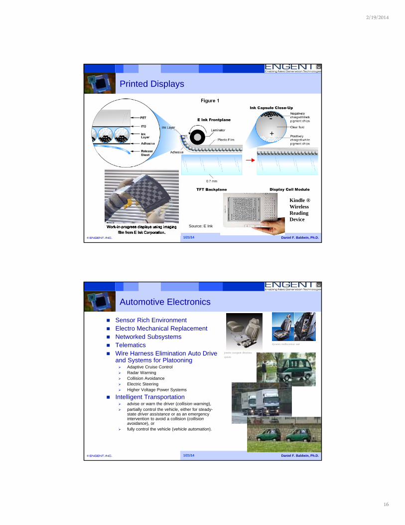
Automotive Electronics
Confidential/Competition Sensitive Daniel F. Baldwin, Ph.D.© ENGENT. INC. 1/21/14
IMUs
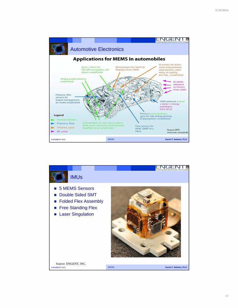
5 MEMS Sensors
Double Sided SMT
Folded Flex Assembly
Free Standing Flex
Laser Singulation
Source: ENGENT, INC.

2/19/2014
18
Confidential/Competition Sensitive Daniel F. Baldwin, Ph.D.© ENGENT. INC. 1/21/14
1000 resevoirs on 10 x 10mm device Preprogrammed drug, reagent, other chemical release
93.280/293bes
Bioelectronics
Bio-sensing/Drug Delivery
Confidential/Competition Sensitive Daniel F. Baldwin, Ph.D.© ENGENT. INC. 1/21/14
Body-Powered Electronic Implant
Managing a power source for a medical implant has been a daunting challenge for many healthcare researchers and scientists. However, new technology from the Massachusetts Eye and Ear Infirmary (Boston) and the Division of Health Sciences and Technology at Harvard-MIT (Cambridge) may change that.
Scientists at the shared research center created a specialized microchip that is powered by the body’s natural chemistry. While the microchip is only able to generate a very small current, the device generated enough current to power a small radio transmitter.
The microchip works by exploiting concentration gradients of potassium and sodium ions in the ear. When an ear is functioning properly, it converts mechanical sound vibrations into an electrochemical signal. This signal can then be sent directly to the brain. One important part of the ear is the cochlea. In the cochlea is a membrane that pumps sodium and potassium ions to create a gradient.
A close-up of a chip, equipped with a radio transmitter, that is powered by a natural battery found in the mammalian ear. (Image by Patrick P. Mercier).
This imbalance of ions creates an electrical voltage that can be exploited by small electronic implants. According to researchers, this voltage is the highest that can be found anywhere in the body. However, this voltage is still extremely low.
2/19/2014
19
Confidential/Competition Sensitive Daniel F. Baldwin, Ph.D.© ENGENT. INC. 1/21/14
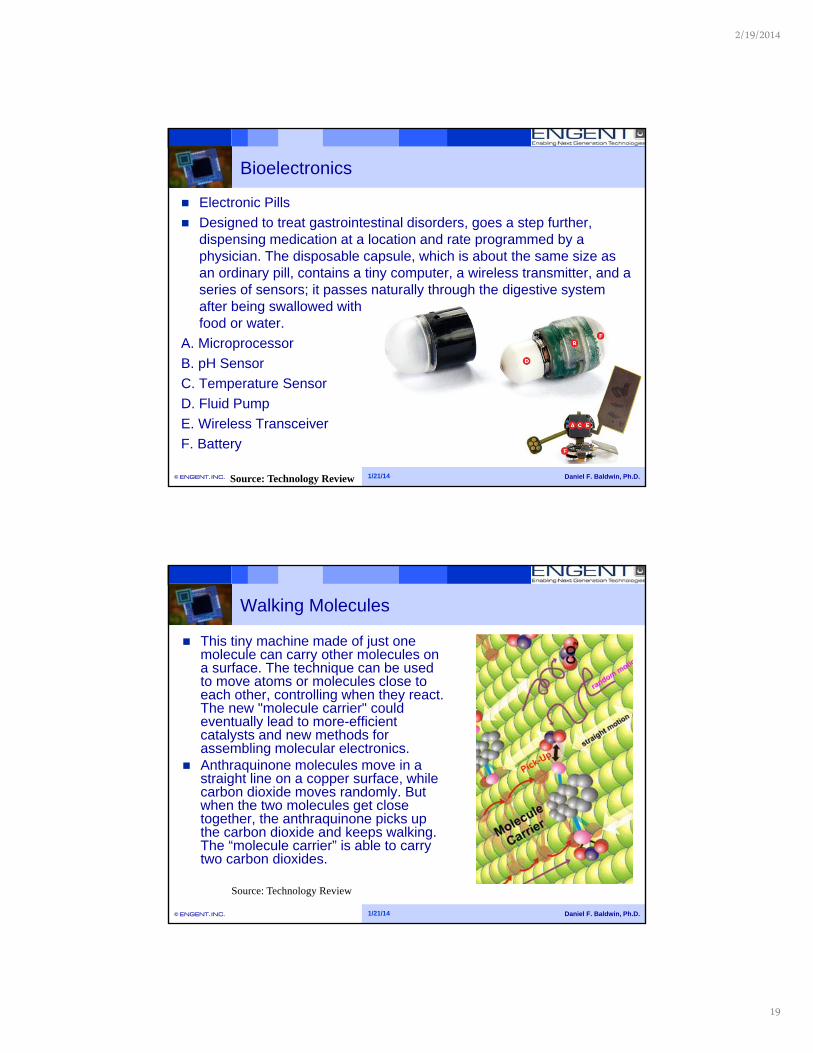
Bioelectronics
Electronic Pills
Designed to treat gastrointestinal disorders, goes a step further, dispensing medication at a location and rate programmed by a physician. The disposable capsule, which is about the same size as an ordinary pill, contains a tiny computer, a wireless transmitter, and a series of sensors; it passes naturally through the digestive system after being swallowed with food or water.
A. Microprocessor
B. pH Sensor
C. Temperature Sensor
D. Fluid Pump
E. Wireless Transceiver
F. Battery
Source: Technology Review
Confidential/Competition Sensitive Daniel F. Baldwin, Ph.D.© ENGENT. INC. 1/21/14
Walking Molecules
This tiny machine made of just one molecule can carry other molecules on a surface. The technique can be used to move atoms or molecules close to each other, controlling when they react. The new "molecule carrier" could eventually lead to more-efficient catalysts and new methods for assembling molecular electronics.
Anthraquinone molecules move in a straight line on a copper surface, while carbon dioxide moves randomly. But when the two molecules get close together, the anthraquinone picks up the carbon dioxide and keeps walking. The “molecule carrier” is able to carry two carbon dioxides.
Source: Technology Review

2/19/2014
20
Confidential/Competition Sensitive Daniel F. Baldwin, Ph.D.© ENGENT. INC. 1/21/14
Nanofluidic Channels for Lab-on-Chip Nanofluidic channels are useful for many
biological and chemical applications, such as DNA sequencing, drug delivery and molecular sensing and detection.
IBM researchers reported a wafer-scale nanochannel fabrication process compatible with CMOS technology on a 200mm wafer-scale sub-20nm nanochannel fabrication method that enables stretching, translocation and real-time fluorescence microscopy imaging of single DNA molecules.
Through the use of sacrificial etching and various UV and e-beam lithography methods, sub-20nm patterns in silicon were converted into macro-scale fluidic ports, micro-scale fluidic feed channels, and nano-scale channels for DNA imaging. Gradient nanopillars were located in the channels to stretch DNA molecules prior to imaging them.
Fluid wasn’t pumped through the channels, but instead was transported by the force of gravity. The researchers say their techniques lead to highly manufacturable structures and can produce chips for a variety of biological applications.
Confidential/Competition Sensitive Daniel F. Baldwin, Ph.D.© ENGENT. INC. 1/21/14
iNEMI Roadmap Packaging & Component Substrates
Functional Diversification (“More than Moore”) is driving rapid change in Packaging and Component Substrate Technology for Consumer products
New Packaging technologies needed to satisfy market requirements include: Wafer level packaging
Wafer thinning
System in Package (SiP)
Printed electronics
Direct bonding interconnect
New conducting materials
New dielectric materials
3D Integration
3D integration will require a combination of new technologies and materials including some defined above
Source: iNEMI

2/19/2014
21
Confidential/Competition Sensitive Daniel F. Baldwin, Ph.D.© ENGENT. INC. 1/21/14
Board Assembly Roadmap Key Trends
Business Environment
Higher level of service demand placed on EMS
EMS companies are expanding offerings to include services in a wider range of a product‘s life cycle
Increased role of EMS/ODM and materials/equipment suppliers in R&D and process development
Continued migration to low cost regions
Demands on cost reduction and low margins are driving consolidation among EMS companies
Source: iNEMI
Confidential/Competition Sensitive Daniel F. Baldwin, Ph.D.© ENGENT. INC. 1/21/14
Board Assembly Roadmap Key Trends
Main Drivers for Development in Board Assembly
Conversion cost reduction
Increased Component I/O Density (miniaturization)
Environmental and regulatory requirements
Reduction in New Product Introduction (NPI) Time
Technology Trends(examples of solutions)
SiP solutions
Embedded components
Flexible tooling solutions
Optimized production equipment sets
Optimized production line configurations
Source: iNEMI

2/19/2014
22
Confidential/Competition Sensitive Daniel F. Baldwin, Ph.D.© ENGENT. INC. 1/21/14
Miniaturization: Passive Size Reduction
From 2012 onwards the “M0201” package will be introduced
Dimensions: 0.2 x 0.1 mm
This is half the size of a “01005” package!
Source: iNEMI
Confidential/Competition Sensitive Daniel F. Baldwin, Ph.D.© ENGENT. INC. 1/21/14
Ultra Thin Capacitors
Available in 2 sizes: “0402” and “0201”
Enables placement below ICs Typical applications: Modules (SiP), mobile phones
Very thin ultra low placement force
Source: iNEMI

2/19/2014
23
Confidential/Competition Sensitive Daniel F. Baldwin, Ph.D.© ENGENT. INC. 1/21/14
Summary
Exciting time for electronics
Advances in electronics technology will continue to drive the industry.
Notable advances Semiconductor Technology
Miniaturization
Display technology
Telecommunication electronics
Smart electronics
Automotive electronics
Bio-electronics