new approaches in the fabrication of ... new approaches in the fabrication of multidimensional smart...
TRANSCRIPT

I
NEW APPROACHES IN THE FABRICATION OF
MULTIDIMENSIONAL SMART MATERIALS FOR
BIOTECHNOLOGICAL APPLICATIONS
Submitted in total fulfilment of the requirements for the degree of
Doctor of Philosophy By
Chris Mallika Bhadra
Department of Chemistry and Biotechnology
Faculty of Science, Engineering and Technology
Swinburne University of Technology
Melbourne, Australia
2016

I
Abstract
The last decade has seen a rapid advance in the different nanofabrication techniques
being developed that cater for the needs of nanotechnology and nanofabrication
technologies. New fabrication approaches have evolved that enable the scale-down
of materials to nanometre sizes and shapes, allowing an exquisite control of their
properties. Nano-fabrication approaches involve various methods of fabricating
nanostructures and engineering devices that have dimensions lower than 100 nm.
The different structures that have been produced and reported so far are diverse, and
serve as an indicator of the versatility that already exists in available micro-
fabrication technologies. There is still, however, significant potential for the
development of advanced two-dimensional and three-dimensional materials with
improved micro- to nano-scale resolution.
This thesis has been primarily devoted to the investigation of three types of newly
fabricated multi-dimensional bio-inspired material surfaces. These materials were:
modified commercially available Grade 2 titanium, black silicon (bSi) and a three-
dimensional (3D) Poly (vinyl alcohol) (PVA)-Vinyl Pyrrolidone (VP) hydrogel. The
titanium and black silicon substrata were modified to possess a structure that was
inspired by the surface nano-pillar pattern found on dragonfly wings. The titanium
surfaces were created using an optimised one-step hydrothermal treatment process,
whereas the black silicon surfaces were produced using a reactive ion etching (RIE)
method. The physical and chemical properties of newly fabricated and/or modified
surfaces were comprehensively characterised using scanning electron microscopy
(SEM), atomic force microscopy (AFM), optical interferometry, Raman

II
spectroscopy, X-ray diffraction (XRD), X-ray photoelectron spectroscopy (XPS),
infrared spectroscopy (IR) and contact angle goniometry. The bactericidal efficiency
of these surfaces against P. aeruginosa ATCC 9027 and S. aureus 65.8T was
evaluated using confocal laser scanning microscopy (CLSM), SEM and viable plate
count assays.
A three dimensional microfluidic device was constructed incorporating bSi. It was
found that this device could be used to eliminate up to 99 % of P. aeruginosa cells
from an infectious dose after 5 successive fill-stop cycles through the device. The
bacterial killing rate was found to be 2.3 × 10³ cfu/min/cm2. The newly designed
microfluidic device could also be used for the effective extraction of protein from
ruptured E. coli cells.
A new mechanism for (indirect) extracellular electron transfer (EET) in a three-
dimensional hydrogel environment was proposed. It was confirmed that the original
polymeric network of the hydrogel was transformed and utilized by G. oxydans
bacterial cells through the active interaction of the bacterial extracellular
polysaccharides with the PVA-VP hydrogel to facilitate the formation of a functional
bio-wire network. The bacterial cells formed remarkable side-by-side, self-organised
bio-wires within the hydrogel system.
The biomimetic and antibacterial surfaces produced in this study were shown to
possess selective bactericidal activity, and the ability to enhance the aligned
attachment behaviour and proliferation of primary human fibroblasts over 10 days of
growth. These antibacterial surfaces, which are capable of exhibiting differential
responses to bacterial and eukaryotic cells, represent surfaces that have excellent
prospects for biomedical applications.

III
Acknowledgements
Words fail me when I yearn to depict my deepest feelings of gratitude for those
people who have given invaluable help, guidance and moral support during this
sojourn in my life. Yet, I shall try to make an effort in thanking each and every one
from the bottom of my heart. Without all of you, this journey would not have
reached where it was supposed to!
To begin with, I would like to acknowledge my greatest appreciation for my
principle supervisor, Professor Elena P. Ivanova for her advice and support during
the tenure of my study. Despite her busy schedule, she always took out time to talk
to me whenever I stumbled upon problems and her inspiration, motivation, and
encouragement were the driving forces pushing me forward towards completion of
this work. She has always been utterly patient with me and the follies I have made,
and has always been there to show me the correct path. Apart from being my
supervisor, she donned various roles in my life starting from a teacher, mentor to that
of an idol. ‘Mam, you have inspired me and shall always continue to do so. I
have looked upon you as my role model and idolized you whole-heartedly. I
wish that one day I am able to make you proud.’ Similarly, I would also like to
thank Professor Russell Crawford, Professor Saulius Juodkazis, and Dr. James Y.
Wang for co-supervising the project, and for spending time helping me on various
manuscripts and experimental protocols. I would also like to thank Dr. Sylvia
Mackie for guiding me through the process of thesis writing and submission. I thank
all of you for your esteemed supervision and guiding me all along until the day when
I am able to write this.

IV
I would like to send my gratitude to Dr. Mohammad Al Kobaisi, Dr. Vi Khanh
Truong, and Dr. Hooi Jun Ng for their knowledge and assistance in operating various
instruments, and techniques. I would also like to thank Dr. James Wang for his
assistance in performing SEM and XRD experiments. Similarly, I would like to
thank Dr. Mark Tobin and Dr. Ljiljana Puskar for helping with our work at the
Australian Synchrotron, FTIR beam line. I would also like to thank Dr. Christian
Garvey for helping with the data analysis of the hydrogel experiments.
Ha and Hayden (Dr. Nguyen & Dr. Webb), you came in my life when I was looking
for someone to share my deepest thoughts and doubts. This friendship is treasured to
me and I consider myself lucky to have found great seniors in both of you.
Vy, I cannot thank you for always being there for me. I have enjoyed every moment
spent in the lab with you. Of course, that each moment spent in the lab with you
made my learning easier. There have been times when my constant asking might
have made life miserable for you, but your support has been a driving force on this
path.
Qudsia, you have been a soul sister for me. You have made all those conversations
look like cakewalk to me, which seemed impregnable before. Thanks for being there
with me, for all conversations big and small. Your courage and determination always
inspired me and made me believe that a lot could be achieved if you are determined.
Peter, Tharushi, Jason, Duy, Nipuni and Miljan, all of you made my journey more
colourful and memorable. I thank all of you for making it worthwhile.
A very big and a heartfelt gratitude to two of the most important people of my
journey so far: Dr. Shanthi Joseph and Dr. Gediminas Gervinskas. Today, I feel

V
and realize that I would not have survived three years had it not been the two of you
by my side. Your honest opinions, suggestions and unparalleled help have made me
see the silver lining out of every dark cloud. Even when you were physically not
present around me, I somehow knew that you were always reachable. In today’s
world where fake pleasantries surround us, you two were the only ones who were
always upfront and honest no matter how harsh the truth was. There have been
moments where I went weak and needed reassurance and a shoulder. You did that to
me and that lies etched in my heart forever. You have filled the gap of an elder sister
and an elder brother, respectively in my life. I feel extremely lucky and blessed to
have met you both. Respect, admiration and love for both of you continue to grow in
my heart. I know that not all dreams come true, but I wish I find people like you
anywhere and everywhere I go.
A note of thanks and gratitude to all the wonderful staff at MCN for helping me
throughout my visits to achieve what I wanted. A special mention has to be made
about Dr. Dan Smith and Dr. Ricky Tjeung for always being there for me, whenever
I needed them around. A lot of my work would not have been possible without their
friendly support and guidance.
A special thanks and gratitude to Ngân, Angela, Soula, Pierrette, Chris, Rebecca and
Katherine and all the laboratory technicians who have helped me with the
experiments and instrument handling throughout the course of this work. To all my
fellow friends in Swinburne, you guys have made my every day more fun and
enjoyable. For the last three years, AS-309 was second home to me. Leaving this
behind is like a heavy boulder on my heart for there are countless memories
engraved. I am yet again thankful to Azadeh, Kaylash, Rue, Nadine, Zaynab, Yen,
Tasnuma, Sanjida, Matthew, Rashida and Guri.

VI
Not to forget some of my closest friends at heart; Kamal, Dibya Di, Pinki and
Piyush. You made me realize that distance is actually just a number. I love you and
feel blessed to have you in my life. There is, however a second family which needs
to be thanked as well. I became a member of this big family when I first arrived in
Melbourne. All of you welcomed me with open hearts and took me in your shelter.
For that, I would specially like to thank Sanjana, Shilpi Boudi and kalyan Da,
Tapashi Di and Rick Da, Mimi Di and Bubai Da and Gopa Maashi and Satinath
Mesho.
I cannot end this section without thanking the oxygen tank of my life and the soul to
my system- Dimma, Mamon, Pappa and Mamma. This would never have been
possible without my family’s support and unconditional love. Living 14,000 kms
away from home is not an easy task, if not for a wonderful family support. It has
been all your love, trust and belief in me that has kept me grounded so far in my life.
I know I cannot repay what you have done for me and no matter how much I thank;
it will all fall short in the end. I love all of you to death and you are all that matters to
me.
Lastly, it seems fitting to thank all of them who thought I could not make it through.
Your constant remarks and looking down upon me only made me stronger. Thank
you!
How could I have forgotten this?
“This is the Lord's doing, and it is marvellous in our eyes.”

VII
Declaration
I, Chris Mallika Bhadra, certify that the work presented in this thesis contains no
material, which has been submitted for another degree of any other university. To the
best of my knowledge, it does not contain any material previously published or
written by another person except where an adequate reference has been made in the
text.
I also declare that I have obtained, where necessary, permission from copyright
owners to use any third party copyright material reproduced in this thesis or to use
any of my own published work in which the copyright is held by another party.
Chris Mallika Bhadra

90
Mumma , Pappa , Dimma & Mamon .
This thesis is because of, and for all of you.

90
List of Publications
Publications from this thesis:
Book Chapters
Vy T.H. Pham, Chris M. Bhadra, Vi Khanh Truong, Russell J. Crawford,
Elena P. Ivanova (2015) Design antibacterial surfaces for biomedical
implant, Antibacterial Surfaces, Springer, USA, ISBN 978-3-319-18593-4,
doi 10.1007/978-3-319-18594-1.
Hayden K. Webb, Chris M. Bhadra, Vy T.H. Pham, Russell J. Crawford,
Elena P. Ivanova (2014) The design of super hydrophobic surfaces, Super
hydrophobic surfaces, Elsevier, ISBN 9780128013311, pp. 27-44.
Peer-reviewed research articles
Chris M. Bhadra, Vi Khanh Truong, Vy T. H. Pham, Mohammad Al
Kobaisi, Gediminas Seniutinas, James Y. Wang, Saulius Juodkazis, Russell J.
Crawford &Elena P. Ivanova (2015) Antibacterial titanium nano-patterned
arrays inspired by dragonfly wings. Scientific Reports, DOI:
10.1038/srep16817.
Xuewen Wang, Chris M. Bhadra, Ricardas Buividas, Thi Hoang Yen Dang,
James Wang, Russell J. Crawford, Elena P. Ivanova, and Saulius Juodkazis.
(2016) Bactericidal Microfluidic Device Constructed using Nano-textured
Black Silicon. RSC Advances, DOI: 10.1039/C6RA03864F.
Vy T. H. Pham, Vi Khanh Truong, Anna Orlowska, Shahram Ghanaati, Mike
Barbeck, Patrick Booms, Alex James Fulcher, Chris M. Bhadra, Ricardas
Buividas, Vladimir A Baulin, Charles James Kirkpatrick, Pauline Doran,
1

2
David E. Mainwaring, Saulius Juodkazis, Russell J Crawford, and Elena P.
Ivanova. (2016) “Race for the surface”: eukaryotic cells can win. ACS
Applied Materials and Interfaces, DOI: 10.1021/acsami.6b06415.
Duy H. K. Nguyen, Vy T.H. Pham, Mohammad Al Kobaisi, Chris Bhadra,
Anna Orlowska, Shahram Ghanaati, Berardo Mario Manzi, Vladimir A.
Baulin, Saulius Joudkazis, Peter Kingshott, Russell J. Crawford, and Elena P.
Ivanova. (2016) Adsorption of human plasma proteins onto nanostructured
black Silicon surfaces. Langmuir, DOI: 10.1021/acs.langmuir.6b02601.
Vi Khanh Truong, Chris M. Bhadra, Andrew Joseph Christofferson, Irene
Yarovsky, Mohammad Al Kobaisi, Chris Garvey, Olga N. Ponamoreva,
Sergey V. Alferov, Valery A. Alferov, Palelle G. Tharushi Perera, Duy H. K.
Nguyen, Ricardas Buividas, Saulius Juodkazis, Russell J. Crawford, Elena P.
Ivanova. (2016) Gluconobacter oxydans self-organizes to form bio-wires for
efficient electron transfer. Scientific Reports (submitted).
Chris M. Bhadra, Marco Werner, Vladimir Baulin, Vi Khanh Truong,
Mohammad Al Kobaisi, Song Ha Nguyen, Armandas Balcytis, Saulius
Juodkazis, James Y. Wang, David E. Mainwaring, Russell J. Crawford, Elena
P. Ivanova (2016) Nano-architecture of Black Silicon surfaces determines
their degree of bactericidal efficiency. Langmuir (submitted).
Conference (verbal and poster) presentation with published
abstracts
Chris M. Bhadra, VI Khanh Truong, T. H. Vy Pham, James Y. Wang,
Saulius S. Juodkazis Russell J. Crawford, Elena P. Ivanova (2015),

3
Antibacterial activity of nano-wired titanium surfaces, Sydney, 5th ISSIB/24th
ASBTE Conference.
Xuewen Wang, Chris M. Bhadra, Song Ha Nguyen, Ricardas Buividas,
Elena P. Ivanova, Saulius Juodkazis (2015), Bactericidal microfluidic chip
integrated with black silicon, Melbourne.
Vy T.H. Pham, Vi Khanh Truong, Alex Fulcher, Chris M. Bhadra, David E.
Mainwaring, Saulius Juodkazis, Russell J. Crawford, Elena P. Ivanova
(2015), In-vitro interactions of eukaryotic cells with the complex nanopillar
geometry of antibacterial surfaces, Sydney, 5th ISSIB/24th ASBTE
Conference.
Chris M. Bhadra, Mohammad Al Kobaisi, Vi Khanh Truong, David E.
Mainwaring, Sergey V. Alferov, Polina R. Minaycheva, Olga N.
Ponamoreva, Valery A. Alferov, Russell J. Crawford, Elena P. Ivanova
(2014), Conductive Gluconobacter microwires for microbial fuel cell
applications, Melbourne, 24th Anniversary World Congress on Biosensors.
Chris M. Bhadra, T. H. VY Pham, Vi Khanh Truong, James Y. Wang,
Saulius Juodkazis, Russell J. Crawford, Elena P. Ivanova (2014),
Investigating the antibacterial behaviour of titanium surfaces containing
nano-wires, Melbourne, ASM (Australian Society for Microbiology),
Australia’s largest microbiology scientific meeting and exhibition for 2014–
Solving the Puzzles.

4
Table of Contents
Abstract…………………………………………………………………………….....I
Acknowledgments………………………………………………………………..…III
Declaration……………………………………………………………………..…..VII
List of Publications…………………………………………………………….…….1
List of Abbreviations………………...………………………………………..…….11
List of Figures…………………...…………………………………………………..13
List of Tables…………...…………………………………………………..……….23
List of Equations…………………………….………………………………...…….24
CHAPTER 1. INTRODUCTION……………………………………25
1.1.Overview…………………………………………………..……………………26
1.2. Aims and objective…………………………………………..…………………28
CHAPTER 2. LITERATURE REVIEW……………………………30
2.1. Overview…………………………………………………………………..…...31
2.2. Review of nano-biotechnology: challenge from micron to the nano-scale….…32
2.2.1. Scale………………………………………………………………..…...…34
2.2.2. Device efficiency and applications……………………………………..…36
2.3. Overview of a few major substrates used in nanofabrication……………….....39
2.3.1. Metallic surfaces……………………………………………….………….39
2.3.1.1. Titanium and its alloys……………………………………..…………39

5
2.3.1.2. Silver………………………………………………………..……....…43
2.3.2. Non-metallic surfaces………………………………………..…..………...45
2.3.2.1. Silicon………………………………….……………..…..…….…......45
2.3.2.2. Graphene………………………………………………………...…....47
2.3.3. Polymeric surfaces…………………………………………………………49
2.3.3.1 Poly vinyl alcohol (PVA)…………………………………………..….49
2.4. Overview of surface nanofabrication techniques for biotechnological
applications……………………………………………………………………….…53
2.4.1. Top-down techniques………………………………………………..…….53
2.4.1.1. Lithography………………………………………………………..….53
2.4.1.1.1. Photolithography……………………………………….…….…..54
2.4.1.1.2. Electron beam lithography……………………………..…..…….55
2.4.1.1.3. Soft lithography……………………………………………..……57
2.4.1.1.4. Colloidal lithography………………………………………..……59
2.4.1.1.5. Nano-imprint lithography……………………………..………….61
2.4.1.1.6. Immersion lithography………………………………………..….63
2.4.1.2. Templating……………………………………………..…………...….65
2.4.1.3. Chemical and plasma etching……………………………………..…...67
2.4.1.4. Anodic oxidation…………………………..……………………..……69
2.4.1.5. Electrospinning……………………………………………………..….71
2.4.2. Bottom-up fabrication techniques………………………………………..….75
2.4.2.1. Hydrothermal reaction…………….………………………….…………75
2.4.2.2. Sol-gel coating……………………………………...……………..……77

6
2.4.2.3. Layer-by-layer assembly……………………...………………………79
2.4.2.4. Atomic layer deposition…………………………………………….…81
2.4.2.5. Physical and Chemical Vapour Deposition (CVD)………………....…83
2.5. Overview of applications of nano-surfaces………………..……………...…....95
2.5.1. Nano-patterned titanium surfaces for use as an implant surface….………95
2.5.2. Bactericidal black silicon surface in a three dimensional microfluidic
device……………………………………………………………………………….98
2.5.3. Use of electro-active bacteria towards designing a microbial fuel cell
(MFC)………………...……………………………………………………..….….101
CHAPTER 3. MATERIALS AND METHODS……………..……104
3.1. Overview……………………………………………………….………..……105
3.2. Materials………………………………………………………………..…….105
3.3. Surface fabrication……………………………………..……………..………106
3.3.1. Nano-patterned Titanium…………………………..……………..………106
3.3.2. Black silicon surfaces…………………...……………….…………..……107
3.3.3. bSi integrated in a microfluidic channel………………….…………….....107
3.3.4. Hydrogel thin films………..……………………………….………..……108
3.4. Surface characterization……………………………..……………….….……108
3.4.1. Scanning Electron Microscopy (SEM)……………………………….….108
3.4.2. Optical profilometry……………………………………………..……….109
3.4.3. Atomic Force Microscopy (AFM)…………………………...…...………109
3.4.4. X-Ray Diffraction (XRD)……………………………..……………...…..110

7
3.4.5. X-ray Photoelectron Spectroscopy (XPS)………………………………111
3.4.6. Synchrotron Radiation Fourier Transform Infrared spectroscopy
(SRFTIR)………………………………………………………………………….111
3.4.6.1. FTIR in attenuated total reflection (ATR) mode……………….…...111
3.4.7. Wettability……………………………………………………..…….…..112
3.5. Bacterial strains and growth conditions……………………………...……….112
3.5.1. Scanning Electron Microscopy (SEM)……………………………..……..113
3.5.2. Raman Microscopy………………………………………...………...……113
3.5.3. Bacterial viability assays………………………………….…………..…..114
3.5.4. Confocal Laser Scanning Microscopy (CLSM)……………………..……114
3.5.5. Statistical analysis……………………………………………………..….115
3.6. Eukaryotic cell growth conditions…………………………………..………..115
CHAPTER 4. FABRICATION AND INVESTIGATION OF
ANTIBACTERIAL ACTIVITY OF BIO-MIMICKED, NANO-
PATTERNED ARRAYS ON TITANIUM…………………..…….117
4.1. Overview………………………………………………………………..…….118
4.2. Mimicking of dragonfly wing nano-arrays on titanium surfaces………..……119
4.2.1. Hydrothermal treatment of titanium surfaces…………….…………..…...119
4.2.1.1. Physical change in surface topography……………………….….…..121
4.2.1.2. Chemical change in surface topography………………………..……124
4.3. Selective bactericidal activity of the titanium nano-arrays……………..…….127
4.4. Summary…………………………………………………………………..….130

8
CHAPTER 5. INVESTIGATION OF PRIMARY HUMAN
FIBROBLAST (pHF) PROLIFERATION ON BIO-MIMICKED,
NANO-PATTERNED ARRAYS ON TITANIUM……………..…132
5.1. Overview……………………………………………………………………...133
5.2. Eukaryotic cell response on the nano-wire arrays present on the titanium
substrate……………………………………………………………………………134
5.3. Nano-arrays serve as focal adhesion points for human fibroblasts……….…..136
5.4. Summary………………………………………………………………………138
CHAPTER 6. EFFECTS OF BLACK SILICON SURFACE NANO-
ARCHITECTURE ON ITS BACTERICIDAL ACTIVITY…..…140
6.1. Overview……………………………………………….…………………..…141
6.2. Comparative analogy between natural and synthetic hierarchical structures…143
6.3. Physico-chemical parameters influence nano-architecture of black silicon..…144
6.3.1. Surface topology……………………………………………………….…144
6.3.2. Surface chemistry…………………………………………….……..…….150
6.4. Nano-architecture dependant wettability………………………….….…….....150
6.4.1. Surface topology affects wettability…………………………..……..……151
6.4.2. Surface chemistry affects wettability……………………….………..…..154
6.5. Nano-structure dependant variable bactericidal activity………………..…….156
6.6. Summary………………………………………………………….……..……161

9
CHAPTER 7. CONSTRUCTION OF A BACTERICIDAL MICROFLUIDIC DEVICE USING NANO-TEXTURED BLACK SILICON……………………………………………………..………162
7.1. Overview…………………………………………………….……….....…….163
7.2. Design and conceptualization of a 3-dimensional bSi microfluidic device…..165
7.3. Bactericidal activity of the bSi embedded microfluidic device……………….169
7.4. Application of bSi microfluidic device towards proteomics………….……....174
7.5. Summary……………………………………………………………..……….177
CHAPTER 8. CONSTRUCTION AND STUDY OF Gluconobacter
oxydans SELF-ORGANIZED BIO WIRES AND ITS
APPLICATION AS A BIO-ANODE IN A MICROBIAL FUEL
CELL (MFC)……………………………………………………………….…..181
8.1. Overview…………………………………………………………………..….182
8.2. Three-dimensional organisation of PVA-VP hydrogels…………….……...…185
8.3. Characterization of PVA-VP hydrogels without and with G. oxydans……….187
8.3.1. G. oxydans biowire network formation and physico-chemical
characterization…………………………………………………………………….187
8.3.2. Swelling ratio analysis………………………………………………...….190
8.4. (Proposed) mechanism of self-organized formation of G. oxydans biowire via
polymeric network…………………………………..……………………….…….192
8.5. Electrical performance of encapsulated G. oxydans as a bio-anode……….....195
8.6. Summary…………………………………………………………...…………197

10
CHAPTER 9. GENERAL DISCUSSION AND
CONCLUSIONS…………………………………………………….199
9.1. Overview………………………………………………………………..…….200
9.2. Bactericidal “smart” materials and applications……………………………....201
9.3. Construction of 3D environments for exoelectrogenic bacteria………...…….209
9.4. Summary and conclusions…………………………………………..………..211
CHAPTER 10. FUTURE DIRECTIONS……………………….…214
10.1. Future scope of this work……………………………………………………215
10.2. Final remarks…………………………………...……………………………216
BIBLIOGRAPHY…………………………………………..….……217

11
List of Abbreviations
AFM Atomic Force Microscopy
SEM Scanning Electron Microscopy
XPS X-ray Photoelectron Spectroscopy
FTIR Fourier Transform Infrared Microscopy
ATR Attenuated Total Reflection
CLSM Confocal Laser Scanning Microscopy
CA Contact Angle
WCA Water Contact Angle
CI Composite Interface
PDMS Poly (dimethylsiloxane)
KOH Potassium hydroxide
CP-Ti Commercially Pure Titanium
HTE-Ti Hydrothermally treated and etched Titanium
b-Si Black Silicon
FFT Fast Fourier Transform
DRIE Deep Reactive Ion Etching
UHV Ultra High Vacuum
MD Molecular Dynamic
PMMA Poly (methyl methacrylate)
UV-LED Ultra-violet light emitting diode
PVA Poly (vinyl alcohol)
PVP Poly (vinyl pyrrolidone)

12
L-PVA-VP Low molecular weight PVA-VP hydrogel
H-PVA-VP High molecular weight PVA-VP hydrogel
CAN Cerium Ammonium Nitrate
USANS ultra-small angle neutron scattering
SAXS small angle x-ray scattering
Au Gold
Sa Staphylococcus aureus
Pa Pseudomonas aeruginosa
E. coli Escherichia coli
GO Gluconobacter oxydans
pHF Primary Human Fibroblasts

13
List of Figures
Figure 2.1. A representative image describing the effects of nano-topography on
cellular activity and protein adsorption. Cell specificity, proliferation and
differentiation have been seen to alter on the nano-structured surface compared to
cellular activity observed on smooth control surfaces. Reproduced with permission
from (Mendonça et al., 2008)………………………………………………………36
Figure 2.2. A hierarchical structuring of nanostructured assemblies. (A) Shows a
honeycomb like pattern on thin polymer films cast in humid conditions. (B) A
paradigm shift in the ordering of hierarchical structure from micron to nano-metre
scale. The hexagonal arrangement of polymer framework can be clearly broken
down into a linear arrangement of individual peptide molecule. A 3D hierarchical
pattern is obtained when poly-ion complexes of bilayer amphiphilic molecules are
engaged. (Reproduced with permission from (Shimomura and Sawadaishi,
2001)……………………………………………………………………….………38
Figure 2.3. Overview of some of the commonly used substrata in nano-fabrication.
(A) Side-view SEM images of Ti nano-pillars anodized at 70V. The pillars are 100
nm tall and have an inter-pillar spacing of 60 nm. Scale bar is 100 nm. (Adapted with
permission from (Sjöström et al., 2009)). (B) SEM images of silver nano-pillars
fabricated by the polyol method with octahedron morphology. Scale bar is 1 µm.
(Adapted with permission from (Wiley et al., 2007a)). (C) Cross-sectional SEM
image of black Si plasma etched for 25 min plasma etching and coated by 100 nm of
gold. The pillar spikes are 3 µm. (permission pending) (D) & (E) SEM images of top
and bottom layers of graphene films. Scale bar is 1µm (Adapted with permission
from (Pham et al., 2015)). (F) 3D freeze-thawed PVA hydrogels with mesoporous
14
morphology. Scale bar is 80-1µm (Adapted with permission from (Holloway et al.,
2013b)……………………………………………………………………………….52
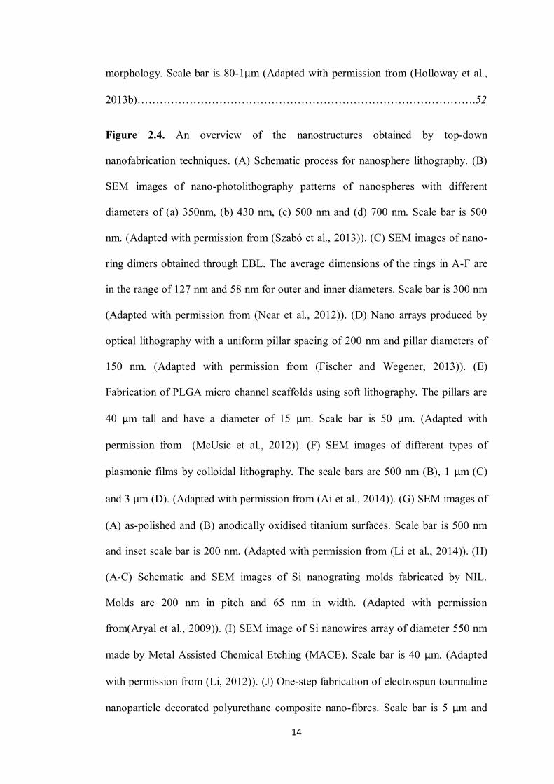
Figure 2.4. An overview of the nanostructures obtained by top-down
nanofabrication techniques. (A) Schematic process for nanosphere lithography. (B)
SEM images of nano-photolithography patterns of nanospheres with different
diameters of (a) 350nm, (b) 430 nm, (c) 500 nm and (d) 700 nm. Scale bar is 500
nm. (Adapted with permission from (Szabó et al., 2013)). (C) SEM images of nano-
ring dimers obtained through EBL. The average dimensions of the rings in A-F are
in the range of 127 nm and 58 nm for outer and inner diameters. Scale bar is 300 nm
(Adapted with permission from (Near et al., 2012)). (D) Nano arrays produced by
optical lithography with a uniform pillar spacing of 200 nm and pillar diameters of
150 nm. (Adapted with permission from (Fischer and Wegener, 2013)). (E)
Fabrication of PLGA micro channel scaffolds using soft lithography. The pillars are
40 µm tall and have a diameter of 15 µm. Scale bar is 50 µm. (Adapted with
permission from (McUsic et al., 2012)). (F) SEM images of different types of
plasmonic films by colloidal lithography. The scale bars are 500 nm (B), 1 µm (C)
and 3 µm (D). (Adapted with permission from (Ai et al., 2014)). (G) SEM images of
(A) as-polished and (B) anodically oxidised titanium surfaces. Scale bar is 500 nm
and inset scale bar is 200 nm. (Adapted with permission from (Li et al., 2014)). (H)
(A-C) Schematic and SEM images of Si nanograting molds fabricated by NIL.
Molds are 200 nm in pitch and 65 nm in width. (Adapted with permission
from(Aryal et al., 2009)). (I) SEM image of Si nanowires array of diameter 550 nm
made by Metal Assisted Chemical Etching (MACE). Scale bar is 40 µm. (Adapted
with permission from (Li, 2012)). (J) One-step fabrication of electrospun tourmaline
nanoparticle decorated polyurethane composite nano-fibres. Scale bar is 5 µm and

15
that of the inset is 2 µm. (Adapted with permission from (Tijing et al.,
2012))……………………………………………………………………..……….74
Figure 2.5. An overview of nanostructures obtained by bottom-up nanofabrication
techniques. (A) (a-d) SEM images of hydrothermally treated ZnO rods before (left)
and after (right) treatments. a, b are top views while c,d are side views. (Adapted
with permission from (Chen et al., 2012b)). (B) SEM images of untreated and treated
PET films with silica films by LBL assembly. Scale bar is 10 µm µm. (Adapted with
permission from (Carosio et al., 2011)). (C) FE-SEM images of ZnO thin films
doped with cobalt via sol-gel spin coating method. Scale bar is 500 nm. (Adapted
with permission from (Poongodi et al., 2015)). (D) SEM images of surface bound
carbon nanowalls made by PECVD having secondary wall-like structures. (Adapted
with permission from (Chuang et al., 2006)). (E) SEM image of the ZnO created 20
nm nanoporous alumina membrane by ALD. Scale bar is 500 nm. (Adapted with
permission from (Narayan et al., 2010))…………………………………...……….87
Figure 4.1. Schematic of liquid hydrothermal treatment process used to fabricate
nano-wire arrays on titanium surfaces…………………………………….………121
Figure 4.2. Surface characterization of AR-Ti and HTE-Ti surfaces. (A) High
resolution optical profilometry images of AR-Ti and HTE-Ti surfaces on a scanning
area of 46.7 µm × 62.3 µm, along with height profiles, indicating the presence of
sharp nanowires on the surface of the HTE-Ti. (B) SEM images of AR-Ti and HTE-
Ti samples. Scale bar is 400 nm. (C) Graphical illustration of water contact angles of
AR-Ti and HTE-Ti surfaces……………………………………………..……….123
Figure 4.3. Regularity of the nano-wire arrays on HTE-Ti surface as analysed using
Image J. (A) SEM micrographs were altered and filtered to analyse the size and

16
angle orientation of the nano-wire arrays. (B) Size distribution (left) and orientation
angle (right) of the nano-wires…………………………………...………………..124
Figure 4.4. Chemical elemental analysis of AR-Ti and HTE-Ti substrates. (A) High-
resolution XPS spectra of titanium reveal the oxidation states of titanium present on
the AR-Ti and HTE-Ti surfaces (B) X-ray diffraction depicting crystallinity of
titanium and titanium dioxide on AR-Ti and HTE-Ti surfaces (alpha (α) phase of
titanium, anatase (A) and the rutile (R) phases of titanium
dioxide)…….………………………………………………………………………125
Figure 4.5. Representative S. aureus (left) and P. aeruginosa (right) attachment
patterns on AR-Ti (A) and HTE-Ti (B) surfaces after an 18 h incubation period.
SEM images represent an overview of the attachment pattern (Scale Bar is 200 nm),
while the CSLM images reveal viable and non-viable cells. Scale Bar is 10 µm.
Individual pie-charts represent the antibacterial activity of both the
surfaces…………………………………………………………………………….128
Figure 4.6. P. aeruginosa cell membrane-nano-wire interaction on HTE-Ti surface
as visualised by FIB-SEM. (A) Top view of a P. aeruginosa cell on HTE-Ti surface
(scale bar is 1 µm). (B-C) P. aeruginosa cell membrane is gradually engulfed by
nanowires on HTE-Ti surface. Scale bars are 200
nm…………………………………………………………………………….…...130
Figure 5.1. Cell adhesion and proliferation pattern of human primary fibroblasts
(pHF) on AR-Ti and HTE-Ti surfaces after 1, 3 and 10-day incubation periods as
shown by (A) CLSM and (B) SEM images. The cell coverage (%) and cell numbers
attached to the respective surfaces are given in (C) and (D)
respectively………………………………………………………………..……….135

17
Figure 5.2. Interaction between primary human fibroblasts and nano-wires on HTE-
Ti surfaces. (A) High-resolution SEM of surface nanowires highlighting anchorage
points of the membrane, scale bar is 1 µm (B) Confocal micrograph showing the
distribution of primary human fibroblasts on nano-surface, with the anchorage points
of vinculin (stained red) (green indicates actin, blue indicates nucleus) ………….137
Figure 6.1. Comparative analysis of the bSi surface nano-architecture. (A, Top) The
upper plane of the surfaces on the SEM images, 20,000× magnifications, and scale
bar is 1 µm. (A, Middle) The distinct morphologies of the nano-pillars present on
each type of bSi surface as seen from the SEM micrographs taken at a tilted angle of
45º (SEM cross-sections) from the baseline, ×30000, scale bar is 200 nm. The inset
shows a schematic depiction of the representative shapes of the nano-pillars present
on bSi surfaces derived from side-view SEM images, highlighting the distinct pillar
morphology including the pillar height and tip width. (A, Bottom) The lower row
shows the average fast Fourier transform of tiles of size 512 x 512 pixels for each of
the species. The centre pixel has been replaced by the averaged grey value. (B)
Radial integration of FFT of the top view SEM images normalized to the peak
intensity. Error bars correspond to the error of the mean value based on single
standard deviation; the background band shows the error range of sample bSi-2
based on the double standard deviation………………………………….……….146
Figure 6.2. Identification and detection of the nano-pillars on black silicon surfaces.
(A) Training set based on SEM images of bSi-3 (×10k magnification) was used to
distinguish pillar tips and free regions between pillars. P: pillar tip; E: empty space
between pillars. (B) Detected pillar tips (red points) on each type of the bSi
surfaces……………………………………………………………………..……...148

18
Figure 6.3. Pair correlation function (Eq. (6.1)) of pillar tip positions as a function of
distance between pair of pillars for bSi-1 and bSi-2 (A) and bSi-3 and bSi-4 (B). The
up- and down arrows indicate approximate positions of the first peak and minima,
respectively………………………………………………………………………...149
Figure 6.4. Typical two-dimensional AFM images (2.5 µm × 2.5 µm scanning areas)
and corresponding cross-sectional profiles of black silicon surfaces. Scale bar is 2
µm………………………………………………………………………………..152
Figure 6.5. AFM topology analysis: bearing ratio as a function of height of nano-
pillars on black silicon surfaces………………………………………….……….153
Figure 6.6. Bactericidal efficiency of black silicon surfaces. (A) SEM images of P.
aeruginosa, S. aureus cells, which appeared to be disrupted through interaction with
bSi surfaces. Scale bar is 200 nm. CLSM images showing the proportion of live and
dead cells, live cells stained with SYTO® 9 (green) and non-viable cells stained with
Propidium Iodide (red). Scale bar is 5 µm. (B) Bactericidal efficiencies of bSi
surfaces were evaluated over a period of 3 h by using a standard plate count method.
(C) Maxima and minima positions of the pillar tip pair-correlation functions of bSi-1
to 4 as illustrated in Figure 6.3............................................................................... 159
Figure 6.7. Cell morphology on control surfaces. Representative SEM images
represent intact and healthy bacterial morphology of (A) P. aeruginosa and (B) S.
aureus on control Si surfaces. Scale bar is 200nm……………………………….160
Figure 7.1. (A) High resolution SEM image (top view) of bSi with a Fast Fourier
Transform (FFT) inset. Side and top view SEM images (bottom) of laser scribed line
used for cleaving 400-µm-thick Si wafer. (B) Micrograph of the assembled chip

19
(top) and assembly schematic (1 to 5) with adhesive film defining the channel height,
t ~15 µm………………………………………………………………..…………168
Figure 7.2. Schematic of filtering a bacterial suspension through the bSi
microfluidic chip followed by subsequent viability tests (A-D). Optical images
showing the viability of P. aeruginosa cells before and after introducing the cells
into the flow channel………………………………………………………………170
Figure 7.3. Bactericidal effect of the microfluidic device. (A) CLSM image of
fluorescently labelled P. aeruginosa cells and (B) SEM image of P. aeruginosa cells
on control silicon surface. Confocal image (C) and SEM (D) images of P.
aeruginosa cells on bSi surface. Confocal images have been taken after 10 min of
cells being in contact with substratum: Si or bSi. Bacterial cells are stained with
SYTO 9 (green) and Propidium Iodide (red) indicating live and dead bacteria,
respectively…………………………………………………………..……………171
Figure 7.4. Bactericidal performance of the microfluidic bSi channel. (A) Log10
reduction of P. aeruginosa cells has been calculated for each set of experiments for 5
cycle runs. (B) The killing rate of bacteria versus number of cycles through the bSi
channel………………………………………………………………………….….173
Figure 7.5. Estimation of total proteins released from E. coli cells. A linear gradient
has been drawn to signify the increasing amount of extracted proteins. Protein
extraction from initial E. coli cells suspension and the Si channel has been included
as controls……………………………………………………………….…………176
Figure 8.1. Synthetic pathway and physical characteristics of mesoporous poly
(vinyl alcohol) (PVA) of molecular weights 67 kDa (L-PVA) and 125 kDa (H-PVA)

20
cross-linked with N-vinyl pyrrolidone (VP). (A) Schematic illustration of the radical
polymerization reaction between linear polymeric PVA and VP to form the hydrogel
PVA-VP. (B) Mesoporous structures of hydrogel were visualised under freeze-
fractured and hydrated states using scanning electron microscopy (scale bar is 5 μm)
and Raman micro spectroscopy (scanning areas of 5 μm × 5 μm), allowing the
visualization of the porosity dimensions of PVA-VP. (C) Pore diameter distribution
of L-PVA-VP and H-PVA-VP estimated using Image J. (D) The difference in pore
diameters between two hydrogels shown by ultra-small angle neutron scattering
(USANS) spectra………………………………………………………….………186
Figure 8.2. Self-assembly of Gluconobacter oxydans sbsp. industrius B-1280 into
biowire clusters in PVA-VP hydrogel systems. (A) Scanning electron microscopy
(SEM) showing the re-organization of G. oxydans into clusters wrapped with
polymer. (B) Confocal laser scanning microscopy (viable cells stained with Syto9®
(green colour) and non-viable cells stained with Propidium Iodide (red colour)) and
(C) Raman micro-spectroscopy (scanning areas: 5 μm × 5 μm) showing G. oxydans
clusters at hydrated states. (D) Cluster length distributions of G. oxydans showing
bacteria forms the shorter length in 67 kDa PVA-VP hydrogel in comparison to 125
kDa PVA-VP. Kinetics of G. oxydans self-organization in L-PVA-VP investigated
using time lapsed (E) CLSM and (F) USANS. (G) Schematic illustration of the re-
arrangement of bacteria disrupting the polymeric
network…………………………………………………………………..……..…188
Figure 8.3. Comparative Raman spectra of G. oxydans (GO) encapsulated in low (L)
and high (H) mol. weight PVA-VP hydrogels and unmodified L- and H-PVA-VP
hydrogels. (A) Raman spectra (at 532 nm laser) of G. oxydans, hydrogel
encapsulated G. oxydans and native hydrogel. (B) Raman imaging in 1600 to 1720

21
cm-1 Raman shift range with the intensity profile map of the same images of
corresponding samples……………………………………………………..……..189
Figure 8.4. Effect of G. oxydans encapsulation on the water retention potential of the
mesoporous PVA-VP hydrogels. Swelling ratios of the PVA-VP hydrogels and their
G. oxydans (GO) encapsulated counterparts……………………………...……….191
Figure 8.5. Time-lapsed self-assembly of G. oxydans in L-PVA-VP hydrogel over a
period of 24 hours………………………………………………………………….193
Figure 8.6. Experimental interactions between bacterial polysaccharide and the
PVA-VP hydrogel. (A) CLSM micrographs showing that the G. oxydans cells (right
image, green colour) completely disrupted the structure of the original hydrogel (left
image), fluorescent SiO2 nanoparticles (red) labelled hydroxyl groups of the PVA-
VP hydrogel. (B) Schematic diagram illustrating the hydrogen bond formation
between the PEG-coated silica nanoparticles and the PVA-VP hydrogel. (C)
Dynamic pH changes of L-PVA-VP and L-PVA-VP + G. oxydans……………….194
Figure 8.7 Microbial fuel cell (MFC) performance analysis. (A) Schematic of
microbial fuel cell set-up, and (B) The long-term stability of encapsulated G.
oxydans showing the electricity generation.………………………………..……...196
Figure 9.1. A schematic representation of the proposed design of nano-pillar arrays
for guiding cell behaviour. (A) (A-D) Steps showing lithographic fabrication of
nano-pillars to provide specific geometry and spacing, surface functionalization of
the NPs to address cell adhesion sites, control of the mechanical properties of NPs by
changing the fabrication parameters and nano-pillar actuation to stimulate cells or to
detect forces exerted by cells on NPs. (E) cross-sectional SEM image of a

22
representative stem cell proliferation and attachment on nano-pillared surface. Scale
bar is 200 nm. (B) Schematic representation of cell proliferation elucidating the
importance of spacing and symmetry of high-aspect-ratio NP arrays, where red
indicates areas of cell adhesion. Cell spreading initiates at early (A) and late (B, C)
stages of cell spreading. On high-density NP arrays where p < dcrit (critical distance),
the filopodia establish focal adhesions with the surface in all directions. On medium-
density NPs at distances between the NPs reaching dcrit, only extensions oriented in
the lattice directions will be able to find the adhesion, while extensions growing in
other directions will be unable to bridge the gap > dcrit. On low-density NP arrays
where p> dcrit, cells can no longer bridge the pillars in any direction; cells penetrate
to the underlying substrate and extend at the floor of the nano-forest. (Adapted with
permission from (Bucaro et al., 2012))……………………………………………205
Figure 9.2. Schematic depiction of a lab-on-a-chip design comprising of multiple
sections for cell, nucleic acid and protein sample identification and quantification.
(Reproduced with permission from (Baratchi et al., 2014))………………….……208

23
List of Tables
Table 2.1. An overview of the achievements and drawbacks of the nano-fabrication
techniques……………………………………………………………….…………88
Table 4.1. Elemental analysis of the AR-Ti and HTE-Ti surfaces……………..…124
Table 4.2. Attachment of bacterial cells onto the AR-Ti and HTE-Ti surfaces.…127
Table 6.1. XPS analysis of bSi surfaces………………………………..…………150
Table 6.2. Statistical analysis of geometrical aspects and surface roughness analysisa
of nano pillars and bSi surfaces……………………………………..…………….155
Table 7.1. Comparative protein extraction from E. coli cells……………..………175
Table 8.1. Power production characteristics of G. oxydans bacteria based biofuel cell
at the suspension and L-PVA-VP encapsulated states……………………………197

24
List of Equations
Equation 2.1 Specific surface area of a micro-scaled device………………………35
Equation 2.2 Feature size (R) for photolithography……………………..…………54
Equation 2.3 Rayleigh’s degree of focus (DOF) used in photolithography………..54
Equation 3.1 Bragg’s law used in X-ray diffraction (XRD)…………………...…110
Equation 4.1 Reaction for alkali hydrothermal reaction………………….………120
Equation 4.2 Reaction for high temperature formation of sodium titanates in an
alkali hydrothermal treatment.………………………………………….…………120
Equation 6.1 Probability distribution function to analyse the position of a
neighbouring pillar on a black silicon surface………………………………..……147
Equation 7.1 Estimation of average thermal velocity in a channel…………….…173
Equation 7.2 Mean displacement of bacteria over time in the channel…………..174
Equation 7.3 Refraction index of a microfluidic channel……………………...…178
Equation 7.4 Relation between pressure and relative velocity in a microfluidic
channel……………………………………………………………..………………178
Equation 8.1 Calculation of swelling ratio of PVA hydrogels……………………190

25
Chapter 1
Introduction

26
1.1 Overview
It has been extensively reported that biofilm formation on medical implant surfaces
by pathogenic bacteria can result in the failure of the implant and in most cases, the
need for its surgical removal. Subsequent complications include systemic infection,
loss of organ function, amputation or death (Campoccia et al., 2013b, Arciola et al.,
2012, Zimmerli and Sendi, 2011, Senneville et al., 2011, Schierholz and Beuth,
2001). These problems are further aggravated by a large number of resistant bacterial
strains (Witte, 1999, Struelens and Denis, 2000, Lora-Tamayo et al., 2013,
Ehrensberger et al., 2015) that have emerged as the result of the increased use of
chemical sterilisation methods (Campoccia et al., 2010, Rams et al., 2014, Hickok
and Shapiro, 2012, Campoccia et al., 2013a, Salgado et al., 2013, Williams et al.,
2013). It is for these reasons that there is a need for innovative approaches for
controlling bacterial colonisation of implant surfaces.
Current technological advancements have allowed the refinement and optimization
of biomaterials in their topological characteristics at macro- and micro-scale levels
(Nikkhah et al., 2012, Vasudevan et al., 2014, Shirwaiker et al., 2011). The ability to
fabricate structures and patterns on the micron scale has triggered a wide range of
scientific investigations in areas such as drug design, detection and control and the
development of lab-on-a-chip devices (Stone and Kim, 2001, Shirwaiker et al., 2011,
Andersson and Van Den Berg, 2004, Duffy et al., 1999, Tao and Desai, 2003,
McAllister et al., 2000). Micro-scale fabrication can be effectively applied to
produce a single or thousands of devices. The engineering hypothesis, therefore,
turns to the design, manipulation, and control of the surface topography on
dimensional scales that are approaching that of molecular levels.

27
A range of studies has shown that the nano-scale surface characteristics of a
substrate can profoundly affect the extent of cell adhesion and proliferation
(Wilkinson et al., 1998, Tejeda-Montes et al., 2013, Reynolds et al., 2013, Chen et
al., 2012a, Hol and Dekker, 2014). Surface nano-scale roughness, which lies on a
scale comparable to that of proteins and membrane receptors, plays a significant role
in cell differentiation and tissue regeneration. The interaction between nano-scaled
surfaces and sub-micron bacterial cells is required to gain a further understanding of
the in vivo bacterial interactions with surfaces. The realization of immense
possibilities of nano-technological systems has so far been inadequate arising from
the complications in their creation and successive assemblage towards fully-
functional structures and devices. The control of nanostructures and ordered
assemblies of materials in two- and three-dimensions still remains elusive and
remains to be studied, despite the promise of science and technology at the
nanoscale.
Nanofabrication involves the production of engineered nanostructures and devices
that have minimum dimensions on a scale that is usually lower than 100 nm
(Mnyusiwalla et al., 2003, Love et al., 2005, Akbarzadeh et al., 2012). This
technology is the basis for nearly every aspect of nanomaterial research and
development, with a focus on their application in complex multifunctional devices.
Nanomaterials are used for applications ranging from microfluidic devices to
molecular diagnostics to nano-diagnostic systems (Mirkin and Rogers, 2001, Gratton
et al., 2008, Tachiki et al., 2003, Sone et al., 1999, Pan and Wang, 2011,
Danilevičius et al., 2013). Of particular interest is the fabrication of structured
surfaces with self-cleaning and antibacterial properties. Much of this state-of-the art
has been inspired by naturally occurring surfaces with self-cleansing and bacteria

28
repelling abilities (Seil and Webster, 2012, Taheri et al., 2014, Hasan et al., 2013a,
Singh et al., 2008, Vasilev et al., 2010).
1.2 Aims and objectives
The main aim of this work was to provide an insight into the fabrication of two- and
three-dimensional hierarchical surfaces. These structured surfaces included titanium
nano-arrays, black silicon and three-dimensional hydrogel systems. Their
applications in industrial and clinical studies in the biotechnology sector were also
investigated. The aim of this work is to successfully construct a working platform,
which could easily combine designed features in the micro- and the nano-scale to
manufacture synthetic metallic and polymeric surfaces that could be applied to the
clinical and biomedical industry. In order to achieve this aim, three intermediate
objectives were identified as key stages toward making such a surface.
The first objective was to characterise the physico-chemical properties of the
fabricated hierarchical nano-structured surfaces. This study involved a number of
techniques, including scanning electron microscopy (SEM), optical profilometry
atomic force microscopy (AFM), wettability, X-ray diffractometry (XRD), X-ray
photoelectron spectroscopy (XPS) and small angle neutron scattering (SANS). This
study provided clear insight on the spatial and the temporal arrangement of the nano-
structured surfaces present on these substrates and their subsequent nano-scale
alignment.
The second objective was to study bacterial interaction with these structured
surfaces. Pseudomonas aeruginosa, a Gram-negative bacterium and Staphylococcus
aureus, a Gram-positive bacterium was used for this assessment. SEM, confocal
laser scanning microscopy (CLSM) and serial plate counting was used to evaluate

29
the efficiency of each surface in regulating the degree of bacterial attachment. This
was a vital link in the study as it generated information about the mechanisms that
cause the killing of the bacterial cells when they were exposed to the fabricated
substrata. It is hoped that this study would pave the way for the design of highly
efficient antibacterial nano-structured surfaces.
The third objective was to evaluate the potential of these structured surfaces towards
the design of biomaterials applicable in the biomedical and biotechnology industries.
The knowledge acquired regarding the mechanisms by which the bactericidal action
occurs represents an important guide for designing surfaces that can control or
prevent the formation of biofilms.
In the following chapters, the current state of knowledge regarding the use of surface
fabrication methods for the generation of nano-structures on titanium, black silicon,
and three-dimensional polymeric hydrogels have been discussed. Following this
discussion, chapters discussing the surface characteristics and properties of
hierarchical surfaces will be presented, along with an analysis of the mechanisms by
which these surfaces were able to control bacterial attachment and mediate bacterial
interaction in an encapsulated state. Finally, possible applications of these unique
surfaces and their possible impact will be discussed, along with future perspectives
of this work.

30
Chapter 2
Literature review

31
2.1. Overview
Nanofabrication plays an ever increasing role in science and technology on the nano-
scale and has allowed the construction of systems of similar complexity as those
found in nature (Chen and Pepin, 2001, Gates et al., 2004, Gates et al., 2005,
Wickson et al., 2010, Kingsley et al., 2013, Srinivasan et al., 1996). Conventional
methods that have arisen from microelectronics are now being used to fabricate
components for integrated circuits, nano-electro-mechanical systems and nano-optics
(Norris et al., 2008, Baruah and Dutta, 2009, Chakraborty et al., 2000, Helvajian et
al., 1997, Helvajian, 1997, Budworth, 1996). Alternative approaches have been used
to modify the techniques and principles that are employed to pattern fine structures
and have brought gratitude for simple and low-cost techniques (Sohlberg et al., 1998,
Merkle, 1996, Jain, 2005, Ramanaviciene et al., 2006, Zhang et al., 2009, Polavarapu
and Xu, 2009, Ni et al., 2007b). This chapter presents an overview of a number of
these methods, with precise attention being given to techniques that enable large-
scale production of nano-patterns on substrate surfaces The chapter begins with a
brief review of the current materials used for nano-fabrication. After reviewing the
various top-down and bottom-up patterning techniques, application areas in the
fields of biotechnology and biomedical industry have been discussed.
Surfaces with super-hydrophobic and self-cleansing properties have gained attention
in the past few decades, owing to their unparalleled potential as templates for the
design of bio-mimetically inspired synthetic surfaces and in material sciences where
substrata and associated devices can exhibit similar properties (Blossey, 2003,
Fürstner et al., 2005, Bhushan et al., 2009, Feng et al., 2002, Nakajima et al., 2000,
Lu et al., 2015, Latthe et al., 2015, Nishimoto and Bhushan, 2013). Such surfaces
have applications that range from self-cleaning glass, anti-fouling coatings and

32
oil/water separation, to high-technology devices, such as anti-wetting and lab-on-a-
chip devices (Lu et al., 2015, Zheng et al., 2015, Banerjee et al., 2015, Wang et al.,
2015, Ferrari and Benedetti, 2015, Zhao et al., 2015, Latthe et al., 2015, Guo et al.,
2015).
This chapter provides an overview of the latest achievements in research fields that
are relevant to the work described in the thesis and showcases a number of examples
for an enhanced understanding of what can be achieved using those techniques.
2.2. Review of nano-biotechnology: challenges from the micron to
the nano-metre-scale
Micro-fabrication has been used to build objects with measurements in the
micrometre to millimetre range (Hutchinson, 2000, Madou, 2002). It takes benefit
from semiconductor fabrication procedures to make integrated circuits, and thus
enhances their specificity by aligning them with processes specially developed for
micro-fabrication (Jin et al., 1998, Clark et al., 2001, Bhagat, 1991). Micro-
fabricated devices, categorized as micro-electromechanical systems (MEMS)
(Spearing, 2000, Judy, 2001, Waits et al., 2005, Wang and Soper, 2006, Baborowski,
2004, Miles, 2004), micro-machines (Rai-Choudhury, 1997, Okandan et al., 2001,
Cohn et al., 1998, Comtois and Bright, 1995), lab-on-a-chip devices (Figeys and
Pinto, 2000, Craighead, 2006, Haeberle and Zengerle, 2007, Mouradian, 2002), and
micro-total analysis systems (micro-TAS) (Reyes et al., 2002, Arora et al., 2010,
Harrison and Van Den Berg, 1998), have existed for more than 30 years, with many
of these applications accomplishing success in scientific and commercial industries.
Although applications were rather limited in biology or medicine during that time-
period, only in the past decade has a closer amalgamation arisen. High-throughput

33
and low-volume-consumption technologies such as whole-genome sequencing
projects and site-specific drug discovery have produced a need for these devices.
Micro-fabrication has spread into two main biological branches: array devices,
which exhibit microscopic arrays of biomolecules immobilized on a surface (Righetti
et al., 2002, Yershov et al., 1996, Heller, 2002, Obeid and Christopoulos, 2003,
Krishnan et al., 2001, Watson et al., 1998), and enclosed fluidic devices
(Selvaganapathy et al., 2003, Cheng et al., 1998b, Hui et al., 2007, Abramowitz,
1999, Becker and Locascio, 2002, McReynolds, 1999, Fiorini and Chiu, 2005).
Micro-fabrication has now penetrated the life sciences, serving as a driving force in
cell biology, neurobiology, pharmacology and tissue engineering for reasons such as
miniaturization, obtaining high surface area to volume ratios, its convenient
integration with electronics, the ability to batch process, deliver small sample
volumes and achieve geometrical control (Voldman et al., 1999, Park and Shuler,
2003, Cheng et al., 1998a, Jensen, 1999, Gravesen et al., 1993). Although micro-
fabrication has been an important milestone to bridge the gap between fabrication
techniques and biological processes, there are reasons why a particular device may
not be micro-fabricated. Firstly, it is possible to conventionally machine these
devices if only a few are required and the dimensions are reasonable (>100 µm).
Secondly, micro-fabrication has extended development times which is dependent on
the system complexity. Finally, the range of micro-structures or materials
manufactured on that scale might not be compatible with the intended application
(Voldman et al., 1999).
The foundation of nano-science was laid by Richard P. Feynman in 1959 (Feynman,
1960), in his famous speech ‘Plenty of room at the bottom’. The term ‘nano-
fabrication’ refers to the tools and techniques that can be used to change the structure

34
and the properties of matter at the nano-scale (≤ 100 nm) (Chakarvarti and Vetter,
1998). Nanotechnology offers the potential to revolutionize the techniques involved
in the fabrication of sensors and devices. Several approaches have been utilised to
fabricate 3D nano-structures, including: modified lithographic processes such as
grey-scale lithography (Poelma et al., 2013, Rammohan et al., 2011), moving mask
lithography (Ito and Okazaki, 2000), multi-photon polymerization (Cao et al., 2009b,
Xiong et al., 2012), laser-induced chemical vapour deposition (Besling et al., 1998,
Kwok and Chiu, 2005, Sosnowchik et al., 2010) and focused ion beam processing
(Frey et al., 2003, Petroff et al., 1991, Utke et al., 2012, Cryan et al., 2005), to name
a few. Despite the success of existing micro-fabrication technologies (Maruo and
Fourkas, 2008, Weibel et al., 2007, Khademhosseini et al., 2006), new techniques
require development as the interest in analysing more complex biological systems,
such as living cells, with nano-fabricated structures has attracted attention and calls
for an in-depth investigation. The two main reasons for this necessary transformation
are scale and device efficiency, which are discussed below:
2.2.1. Scale
Important procedures can take place in mechanical systems that may have
dimensions similar to a physical, chemical or biological process. One such example
includes the attachment or spreading of a eukaryotic cell (Xia et al., 1999, Chen et
al., 1998, Ostuni et al., 2009, Chen et al., 1997) onto structures that are larger than
macromolecules (∼ 2-20 nm) but are smaller than, or equal to, eukaryotic cells (∼ 1-
50 µm). Such structures are commonly known as meso-systems (Vallet‐Regí, 2006,
Imry, 1997, Whitesides and Boncheva, 2002, Venturoli et al., 2006). Fabrication and
examination of these systems has become a vigorous area of research in physics,

35
materials science, chemistry and biology since these systems tend to bridge the gap
between the molecular and the macroscopic world. Nano-systems are defined as
having features or characteristic dimensions between 1 and 100 nm (Chen and Pepin,
2001, Wilkinson and Curtis, 1996, Wilkinson, 1995, Mirkin and Rogers, 2001). In
vivo, cells are bound to an array of scaffolds recognised as being an extracellular
matrix (ECM), wherein every individual ECM component exists in the nano-meter
length scale, enabling appropriate tools from nanotechnology to be able to mimic
their features (Sniadecki et al., 2006, Mendes, 2013, Akhmanova et al., 2015, Santos
et al., 2011, Stevens and George, 2005). Materials with nano-sized dimensions have
piqued interest as the physico-chemical properties of a material change in this
transition system between the bulk and molecular scales (Kuchibhatla, 2008).
The number of atoms at the surface increases with the increase in surface area per
unit volume, when a system dimensions are reduced to nano-scale as described in
Equation 2.1:
Specific surface area= (4𝜋𝑟^2)/(4/3𝜋𝑟^3) = 3
𝜌𝑟; (2.1)
Where, r denotes the radius and 𝜌 denotes the effective surface area of the device.
When dimensions decrease from the micron to nano-metre level, the specific surface
area increases by 3 orders of magnitude (Kuchibhatla, 2008, Chen and Mao, 2007).
This increase in surface area and resulting change in surface free energy leads to a
reduction in the interatomic distance for metals (Uskoković, 2013). On sufficiently
small scales, this leads to a situation where surface effects dominate volume effects
and remarkable physical enhancements result (Voldman et al., 1999, Sekhon et al.,
2010). A greater nano-structured device surface area enables greater cellular
interaction, which leads to an enhanced contact guidance at the cell-substrate

36
interface (Hoffman-Kim et al., 2010, Bettinger et al., 2009). Cell–nano-topography
interactions such as cell morphology, migration and adhesion vary with feature
geometry of the base substrate, as shown in Figure 2.1 (Bettinger et al., 2009, Dalby,
2005, Yim and Leong, 2005, Mendonça et al., 2008) .
Figure 2.1. A representative image describing the effects of nano-topography on cellular activity and protein adsorption. Cell specificity, proliferation and differentiation have been seen to alter on the nano-structured surface compared to cellular activity observed on smooth control surfaces. Reproduced with permission from (Mendonça et al., 2008).

37
2.2.2. Device efficiency and applications
Extensive application of nanofabrication has conceived prospects for an unequalled
development of information technology and micro and nano-electronic devices (Lee,
2011, Ahmed, 1997, Lu and Lieber, 2007, Yu and Meyyappan, 2006, Ludwig and
Meyer, 2011) with specific interests in nano-medicine followd by a special target on
personalized health care, optics, functional substrata with tuneable properties and
bio-chemical based sensors (Kumar et al., 2006, Silva, 2004, Fine et al., 2013, Adiga
et al., 2009, Singh and Nalwa, 2011, Luo et al., 1996) .
From a biomedical point of view, the primary reaction of eukaryotic cell lines on
micro-metre-range topological features such as grooves, ridges and wells has been
well established for decades (Ito, 1999, Whitehead et al., 2005, Von Recum and Van
Kooten, 1996, Kulangara and Leong, 2009). The impact of nanotechnology arises
from the spatial and temporal scales being considered: materials and devices
fabricated at the nano-scale offer an ordered manipulation down to the atomic level
in how they are organized to give shape to a macroscopic substrate as shown in
Figure 2.2 (Silva, 2004). Nano-scaled alterations in topography produce a varied
range of cell behaviour, such as changes in cell adhesion and orientation, cell
motility, cytoskeletal condensation, activation of tyrosine kinases, and intracellular
signalling pathway modulation to control transcriptional activity and gene expression
(Stevens and George, 2005). As a result, nano-scaled substrates can be processed to
demonstrate specific bulk physico-chemical properties due to their ability to control
the organization of their molecular synthesis and assembly (Li et al., 2004, Jung and
Ross, 2007, Camden et al., 2008, Lehn, 2002). Nano-fabrication has simultaneously
given rise to bio-mimetics, where studies are being undertaken to determine the

38
mechanisms by which a synthetically designed nano-structured surface could be used
to control cell behaviour, much like some of the naturally occurring anti-cleansing
and antibacterial surfaces (Bhushan and Jung, 2011, Rahmany and Van Dyke, 2013,
von der Mark et al., 2010, Sleytr et al., 1999, Bhushan, 2009).

39
Figure 2.2. A hierarchical structuring of nanostructured assemblies. (A) Shows a honeycomb like pattern on thin polymer films cast in humid conditions. (B) A paradigm shift in the ordering of hierarchical structure from micron to nano-metre scale. The hexagonal arrangement of polymer framework can be clearly broken down into a linear arrangement of individual peptide molecule. A 3D hierarchical pattern is obtained when poly-ion complexes of bilayer amphiphilic molecules are engaged. (Reproduced with permission from (Shimomura and Sawadaishi, 2001).

40
.2.3. Major substrata used in nanofabrication
This section presents an overview of some of the commonly used metallic, non-
metallic and polymeric substrata in nanofabrication techniques.
2.3.1. Metallic surfaces
Metallic devices are omnipresent in science and technology. Rigorous research is
being undertaken for synthesis of topography controlled metallic nanostructures
(triangles, cubes, tubes, wires, rods, fibres, etc.), their self-assembly, properties and
applications. Recently, the capability to model, fabricate, and characterize metallic
structures at the nano-scale has advanced progress in material, optical, and chemical
sciences (Xia and Halas, 2005, Hecht et al., 2011, Lindquist et al., 2012, Tokonami
et al., 2012, Guo et al., 2014). This ability to control the size, shape and distribution
of the metallic nano-structures provides opportunities to systematically investigate
the catalytic and electro-optical properties and to discover new applications in the
form of novel research techniques and consumer oriented medical devices (Valiev et
al., 2008, Cao et al., 2009a, Valiev et al., 2012). This section covers two of the most
commonly used metallic substrata used in nanofabrication: silver and titanium
surfaces.
2.3.1.1 Titanium and its alloys
Titanium is a widely used orthopaedic implant surface due to its biocompatibility,
toughness and strength-to-weight ratio (Budinski, 1991, Brunette et al., 2012,
Kasemo, 1983, Ratner, 2001, Niinomi, 1998, Hirth and Froes, 1977, Davim, 2014).
Wide band gap semiconductor Titania (TiO2), known as titanium (IV) dioxide, is
also an useful functional material (Galstyan et al., 2013, He et al., 2013b, Cabaleiro

41
et al., 2013, Hwang et al., 2012). When compared to its bulk counterpart, TiO2
nanostructures can be shaped with meticulous dimensions, including nanoparticles,
nanowires and nanotubes, that possess larger surface area to volume ratios, thereby
providing additional reactive sites for catalysis, sensing, and increasing miscibility
with other materials (Nakata and Fujishima, 2012, Nie et al., 2013, Jassby et al.,
2012, Kumar et al., 2013b, Ong et al., 2014). The high surface area brought about by
small particle sizes is advantageous for TiO2-based devices, as it streamlines the
reaction/interaction between the devices and the interacting media, taking place
either on the surface or at the interface and thus, depends on the surface area of the
material. Hence, the performance of TiO2-based devices is influenced by TiO2
building unit dimensions at the nano-scale. With the help of advanced nano-
electronics fabrication technologies such as electron-beam lithography, it is possible
to fabricate well-defined and ordered titanium based nanostructures down to a
possible lateral feature size of 10-20 nm (Rani et al., 2009). Titania nanotubes (Mor
et al., 2003, Tan et al., 2012, Wang et al., 2004a), nanorods (Chu et al., 2005, Yu et
al., 2009, Liu and Aydil, 2009), nanowires (Xu et al., 2003, Armstrong et al., 2004,
Chung et al., 2008) and nano-belts have all been synthesized along with various
titanates (Weng et al., 2006, Mao et al., 2006, Bavykin and Walsh, 2010) and
nanotube composites (Yu et al., 2007, Ramı et al., 2004). They also find applications
in the areas of gas sensors (Galstyan et al., 2013, Perillo and Rodriguez, 2012, Wang
et al., 2013b, Bayata et al., 2014), hydrogen generation (Haidry et al., 2012, Şennik
et al., 2014, Mou et al., 2014, Ni et al., 2007a), photo catalysis (Wold, 1993,
Hashimoto et al., 2005, Woan et al., 2009) and dye-sensitized solar cells (DSSC)
(Mor et al., 2006, Kuang et al., 2008, Koo et al., 2008).

42
1D and 2D nano-materials such as nano-tubes and nano-wires have received much
attention due to their physical properties and applications (Lee et al., 2014). Sol-gel
methods and an anodic alumina membrane (AAM) template have been combined to
produce TiO2 nano-rods by dipping porous AAMs into a boiling TiO2 sol followed
by drying and heating (Kangarlou and Rafizadeh, 2012, Cao and Liu, 2008). The
porosity of an alumina template is used to control the size of TiO2 nano-rods, which
are produced in sizes ranging between 100- 300 nm in diameter. Superior-grade
template constructs are employed to design nano-rods of smaller dimension.
Alternatively, the electrophoretic deposition of TiO2 colloidal suspensions into the
AAM porous scaffold results in the formation of ordered TiO2 nano-arrays. Anatase
nano-rods can be obtained under low temperature conditions, while under high
temperature conditions, rutile nano-rods are obtained in this method (Kumar et al.,
2014, Sun et al., 2013). TiO2 nano-structures, such as nanowires have also been
synthesized via a hydrothermal method. TiO2 white powders are usually treated in
highly alkaline solutions, either 10-15 M NaOH or KOH aqueous solutions, at a high
temperature for 24-72 hours in a steel autoclave. The fabrication of hydrothermally
treated TiO2 nanowire from layered H2Ti3O7 (titanate) has three procedural steps: (i)
layered Na2Ti3O7 exfoliation; (ii) nano-sheet formation; and (iii) nano-wire
formation. In Na2Ti3O7, TiO6 octahedral layers are held together by static
interactions occurring between the Na+ cation and the TiO6 octahedral layers and the
TiO6 unit itself. When larger H3O+ cations replace the Na+ cations in the interlayer
space between the TiO6 sheets, a static interaction becomes destabilized because of
an increase in the interlayer distance. As a result, the layered Na2Ti3O7 sheets are
sequentially scaled out. Next, when Na+ is exchanged by H+ ions in dilute HCl
solution, a number of H2Ti3O7 sheet-shaped products are formed. These nano-sheets

43
gradually split to form nanowires to release stress and achieve a lower energy state
(Ou and Lo, 2007, Horváth et al., 2007, Wu et al., 2006, Wei et al., 2004).
Anatase titania 3D nanostructures have been fabricated through a facile
hydrothermal treatment followed by an annealing process at 550 C. These
nanostructures are formed by the self-organization of several radially distributed
nano-sized petals with larger surface area. The important precursors to fabricate
these uniform nano-flowers are H2O2, Ti powder, and NaOH. H2O2 and NaOH
usually corrode the surface of Ti powders when the reaction commences. The TiO32-
ion concentration increases with time and is deposited on the Ti particles, thus
producing TiO2 nano-flakes (Fattakhova-Rohlfing et al., 2014).
A 3D > 2D > 1D mechanism for the formation of TiO2 nanotubes has also been
described in detail. Raw TiO2 is initially converted into lamellar structures and then
rolled to form nano-tubes with the application of a high voltage as shown in Figure
2.3 (A). The presence of 2D lamellar TiO2 is crucial to enable TiO2 nanotubes to be
produced. One theory proposes that TiO2 nano-tubes can be produced by rolling up
one layer of a TiO2 sheet using a rolling-up vector, which subsequently attracts other
sheets around the tube. A second theory states that nano-tubes could be formed due
to the successive wrapping of multi-layered nano-sheets rather than scrolling or
wrapping of a single nano-sheet followed by layer crystallization (Chen and Mao,
2007, Fattakhova-Rohlfing et al., 2014). Titanium nanostructures have been used on
a broad platform mostly for orthopaedic and dental implants, lithium ion batteries
and electronic equipment (Valiev et al., 2008, Kim et al., 2008, Kulkarni et al., 2015,
Umar and Hahn, 2010, Anpo and Kamat, 2010).

44
2.3.1.2. Silver
Silver nanostructures are fabricated via different techniques such as lithography,
photochemistry, thermochemistry, sonochemistry, wet-chemistry, biochemistry and
electrochemistry (Zhu et al., 2000, Naik et al., 2002, Rodriguez-Sanchez et al., 2000,
Ivanova and Zamborini, 2009). Electrochemistry, ultrasound assisted reactions and
microwave- assisted methods are mostly preferred as they regulate the driving forces
for the reduction of precursor ions, nucleation and growth modes. These phenomena
are comparable to using capping agents to activate reduction and growth kinetics, but
at the same time are different in that control is applied over ranges in parameter
spaces, allowing formation conditions to occur far from thermodynamic equilibria.
These methods are also non-toxic in nature and output products of extra pure quality
can be obtained if proper control is exerted through physical means (Zhou et al.,
2011, Saifuddin et al., 2009, Saha et al., 2013, Helmlinger et al., 2016). Strategies to
administrate the anisotropic growth of silver nanoparticles include templating against
several types of 1D structures, alumina channels, carbon nanotubes, block
copolymers, DNA chains and peptide fibrils. Some purification steps are, however,
needed to extract the final silver nanowires as these techniques can yield smaller
colloidal particles, which can be removed by centrifugation and washing (Mousavi-
Kamazani et al., 2015).
Accurate control over the parameters of the nanostructure enables complete
regulation over its surface properties and adequate applications. Seed crystallization
and the rate of atomic seed addition can be manipulated from which nano-structures
grow to fabricate a number of miscellaneous shapes such as pentagonal nano-wires,

45
cuboctahedra, nano-cubes, nano-bars, bi-pyramids, and nano-beams via a solution-
phase polyol synthesis (Wiley et al., 2007a, Wiley et al., 2005a). This method
influences size, aspect ratio, and shape of the nanostructures. The seed crystal
structure is transferred to the product via epitaxial overgrowth if the crystal structure
and lattice constant of the deposited metal and the seed are similar. The resulting
nano-pattern can still be different from that of the initial seed as the crystal pattern is
governed by the growth rate of crystallographic facets (Chen et al., 2007, Rashid and
Mandal, 2007, Wiley et al., 2006, Wang et al., 2013a, Rycenga et al., 2011).
Conversely, a polyol mechanism involves a heated polyol, salt precursor and a
polymeric capping agent to formulate metal colloids and the subsequent Ag+ ion
reduction process results in the growth and nucleation of Ag nanostructures as
shown in Figure 2.3 (B) (Schuette and Buhro, 2014, Gómez-Acosta et al., 2015).
Commonly occurring agents such as ethylene glycol (EG), AgNO3, and poly (vinyl
pyrrolidone) (PVP) serve as salt precursors and polymeric capping agents,
respectively. Glycoaldehyde as a reducing agent helps in the temperature
dependence of the polyol synthesis method (Wiley et al., 2005b, Lim et al., 2014,
Schuette and Buhro, 2014).
There has been a detailed study on the use of silver nano-cubes as templates in the
synthesis of gold nano-boxes and iron nano-cubes as building blocks of magnetic
super latices and as antibacterial surfaces. Silver nanoparticles (NPs) such as disks,
prisms, and plates attract interest as their properties are dependent on particle shape
and size. The face-centred cubic (fcc) structure of metallic silver assembles its
inclination to nucleate and grow into NPs with their surface bound by the lowest-
energy facets, like the wet chemical synthesis, being mainly confined to those of the
preparation of nanowires, rods, or spheres (Song et al., 2015, Sun et al., 2012, Sun et

46
al., 2003, Wiley et al., 2007b, Sadeghi et al., 2009). The bactericidal effect of silver
ions on micro-organisms has been very well explored but the mechanisms
responsible for their bactericidal behaviour is only partially understood. It has been
elucidated that silver ions have a strong interaction with the thiol groups present on
enzymes, hence rendering them inactive (Morones et al., 2005, Rai et al., 2009,
Sondi and Salopek-Sondi, 2004).
2.3.2. Non-metallic surfaces
2.3.2.1. Silicon
Silicon based nano-patterns possess certain attributes, such as electro-mechanical
properties, biocompatibility and high surface-to-volume ratios with desirable surface
topologies (Priolo et al., 2014, Amato et al., 1998, Irrera et al., 2006, Sham et al.,
2004). These properties have led to the fabrication of efficient nanomaterials in
applications ranging from electronics to biology (Koshida, 2008, Conibeer et al.,
2006, He et al., 2010, Rao et al., 2006). Laser ablation-assisted vapour-liquid-solid
(VLS) growth has been commonly reported for single-crystal silicon nano-wire
(SiNWs) synthesis, producing wires with an average diameter of 6-20 nm and length
of 1-30 m. This approach has been used for the fabrication of SiNWs because of a
high throughput range. Metals and their compounds (e.g., Fe, Au) have been used as
catalysts in order to allow the definition of the diameter of wires produced using this
process. The SiNWs continue to grow as long as the source of Si vapour is available.
This process incorporates different reaction temperatures for nano-wire fabrication
because of the distinct melting temperatures of the catalytic metals (Milewski et al.,
1985, Li et al., 2003, Ishiyama et al., 2014, Kim et al., 2016). The oxide assisted

47
growth (OAG) method is also a familiar approach for the fabrication of nanowires
and is a complementary approach to VLS. In this method, the oxides play a crucial
role as they help to augment the development of the nanowires. This method has
certain advantages over the VLS approach: the nanowires obtained are free of
metallic impurities and can be fabricated by a facile vaporization technique and the
production of altered nano-patterns such as rods, chains and ribbons is also possible
(Zhang et al., 2003, Yao et al., 2005, Ma et al., 2002).
Deep reactive ion etching (DRIE) is commonly used to generate deep, steep sided
features in wafers, with high aspect ratios (Figure 2.3 (C)). Halogen-based plasmas
are used for the etching of silicon due to their high etching rates. They can form
volatile etching products such as SiF4 (Ayon et al., 1998, Klaassen et al., 1996). F-
based plasmas such as SF6 are used for fast isotropic etching. Plasmas such as Cl2
and HBr are used to obtain anisotropic etching profiles due to their ion-induced
etching behaviour (Marty et al., 2005, Jansen et al., 1995, Jansen et al., 2009).
Etching of silicon requires a passivating layer which is designed either by (i) gas
inclusion in plasma to act as silicon oxidant forming non-volatile siliconoxy-
halogens, (ii) freezing the volatile end products at the structure’s walls using
cryogenic wafer cooling method, (iii) gas insertion to act as polymer precursor and
subsequently form carbon–halogen layers or (iv) erosion and redepositing mask
material such as metal halogens. Inhibitor gas insertion is usually carried out in two
etching methods. The first is known as the mixed mode DRIE (e.g. SF6 + O2),
wherein oxygen, which acts as the inhibitor is added at the same time as the etchant
(Laermer and Urban, 2003, Jansen et al., 1996, Chen et al., 2002). This method has
been used in the fabrication of nano-pillared silicon patterns, also popularly known
as the ‘black silicon method’ (Jansen et al., 1995). An alternative technique is the

48
pulsed-mode DRIE (e.g. SF6/C4F8), wherein the inhibitor is presented sequentially
from the etchant and a strong polymer-building fluorocarbon gas is used.
A number of fabrication methods have also been developed for the production of
silicon quantum dots. Methods include solution-phase reductive, plasma-assisted
aerosol precipitation, micro-emulsion, mechano-chemical, laser ablation and sono-
chemical synthesis (Cho et al., 2008, Angus et al., 2007, Darbandi et al., 2005, Koole
et al., 2008). The need for surface chemical modification provides a novel way to
study the relationship between the surface effects and optical properties of quantum
dots, paving the way to functionalize the SiQDs as tailored for different applications.
2.3.2.2. Graphene
Graphene is the generic term allotted to a 2D sheet of sp2 -hybridized carbon (Figure
2.3 (D), (E)). Its honeycomb structure is the foundation for other allotropes (Gracia-
Espino et al., 2013, Stankovich et al., 2006, Avouris and Dimitrakopoulos, 2012).
2D graphene can be arranged to form 3D graphite, rolled to form 1D nanotube and
can also be wrapped to form 0D fullerenes. Long-range π-conjugation in graphene is
the basis for its thermal, mechanical, and electrical properties, which remain the
principal area of research (Rao et al., 2014, Loh et al., 2010, Gracia-Espino et al.,
2013). There have been attempts to fabricate graphene through other techniques
other than the conventional exfoliation and different CVD processes (Park and
Ruoff, 2009, Dong et al., 2010, Yan et al., 2012, Chang and Wu, 2013, Shen et al.,
2013, Botas et al., 2013, Song et al., 2012). Chemical methods have been used to
extract graphene films from graphite without the exfoliation step, as shown by
Horiuchi et al. to produce graphene when forming carbon nano-films (CNF) from
natural graphite (Horiuchi et al., 2004). Natural graphite has been exposed to a
49
number of oxidation and purification processes followed by methanol dilution and
centrifugation steps to remove the thinnest sheets from the dispersion. CNF
thickness is directly proportional to the dilution factor and the resulting end-product
can possess up to 6 layers of graphene. In another study, sulphuric and nitric acid
were intercalated between the layers of graphite, followed by rapid heating to 1000
C, so that volatile acid evaporation could produce thin graphitic sheets (Shin et al.,
2013, Hong and Chung, 2015, Choi et al., 2010). This technique can be used to
fabricate graphene in large quantities. Chemical exfoliation has also been employed
to produce graphene by thermal expansion of graphite oxide via rapid heating at
1050 C, followed by a two-stage reduction process using hydrogen gas and N-
methylpyrolidone (Mowry et al., 2013, Botas et al., 2013). This study pointed out
that the lateral size and crystallinity of the graphite is the governing factor
determining the number of graphene layers to be formed. Epitaxial growth of
graphene on this surface resulted in the formation of 1 to 3 graphene layers, with the
number of layers being dependent on the decomposition temperature used (Wu et al.,
2008, Cambaz et al., 2008, Morita et al., 2013). A detailed review on this process
was provided by Hass et al (Hass et al., 2008).
Graphene is utilized in electronic materials such as transparent conductors and
ultrafast transistors. The applications of graphene and graphene oxide have forayed
into biomedical areas such as bio-sensing through graphene-quenched fluorescence,
graphene-induced cell differentiation and proliferation, graphene-based bio-sensing
devices and graphene-assisted laser desorption/ionization for mass spectrometry due
to their aqueous processability, amphiphilicity, surface functionalizability, surface
enhanced Raman scattering (SERS), and fluorescence quenching ability (Shan et al.,
2009, Rao et al., 2014, Chung et al., 2013) . Although several questions need to be

50
answered, preliminary results in these areas suggest potential for graphene and its
derivatives in biomedical research.
2.3.3. Polymeric surfaces
2.3.3.1. Poly (vinyl) alcohol (PVA)
Polyvinyl alcohol (PVA) is a linear synthetic polymer created by the partial or full
hydrolysis of polyvinyl acetate to remove the acetate groups. The degree of cross-
linking takes control of the physical, chemical, mechanical and biological properties
of the polymer chain. The extent of cross-linking renders PVA its solubility in water
but is immiscible in most of the organic solvents (Bauer et al., 1996, Arima et al.,
2011, Sun et al., 2015, Lee et al., 2009, Karimi and Navidbakhsh, 2014, Baker et al.,
2012). PVA has often been found to cross-link with other chemical components to
form porous hydrogels, shown in Figure 2.3 (F). The physico-chemical crosslinkages
provide the structural stability required by the polymeric hydrogel after it swells in
water or biological fluids. Techniques such as polymer gelation, freeze-thawing,
chemical crosslinking or physical methods such as use of hydrostatic pressure have
been commonly used to produce chemically or physically cross-linked PVA
hydrogels and have been shown to produce stable PVA hydrogels with varied
molecular weights and concentrations (Hassan and Peppas, 2000b, Hassan and
Peppas, 2000a, Negishi et al., 2014, Ino et al., 2013, Kenawy et al., 2014). The
differences in the molecular weight and degree of cross-linking has an effect on the
swelling ratio and Young’s modulus of the polymer hydrogel as the amount of water
absorbed by a dry hydrogel is inversely proportional to the degree of the cross-
linking of the polymer chains. A wide range of hydrogel is thus possible; soft

51
hydrogels with 10% polymer and hard, complex hydrogels consisting of 50%–60%
polymer are possible (Smetana, 1993, Karimi et al., 2013, Shi and Xiong, 2013).
Although PVA hydrogels can bear similar mechanical properties resembling some
soft biological tissues, in order to mimic other tissues and, in particular, for medical
device applications, further improvement of hydrogel durability is required. One
approach has been used to create a PVOH-based nano-composite that retains the
mandatory properties (Swapna et al., 2015, Deshmukh et al., 2015, Fortunati et al.,
2013). Reinforced PVOH nano-composites have been shown to have their
mechanical properties tuneable over a broad range which makes it suitable for
replacing different tissues. PVA can be cross-linked with different compounds such
as glutaraldehyde to control the mesh size morphology and transport properties of
the three-dimensional membrane (Dai and Barbari, 1999, Siró and Plackett, 2010).
Adequate care, however, needs to be taken to eliminate the residual glutaraldehyde
being formed, due to its toxicity. These membranes provide a biocompatible and
size-selective macro-encapsulation membrane for bio-artificial organs and cell
encapsulation. Due to their mesoporous configuration, PVA hydrogels have been
used in the fabrication of three-dimensional scaffolds to act as a bio-anode in
microbial fuel cells (MFC). The porous scaffold acts not only as a cyto-compatible
cellular matrix for reversible bacterial encapsulation but also as an electron transfer
mediator between the bacteria and the surface of bio-electrodes. An enhanced
electron interaction with the bio-anode through the porous scaffold helps to improve
electron transfer, compared to that obtained when applying a biofilm on the electrode
(Lin et al., 2012, Heller, 2006, Gohil and Karamanev, 2015, Alferov et al., 2014).
PVA hydrogels are used for a number of biomedical applications such as contact
lenses and synthetic vitreous humour, artificial pancreases, haemodialysis and also

52
implantable medical materials as a substitute for cartilage and meniscus tissues. PVA
is a desirable polymer for these applications as it is biocompatible and has low
protein adsorption properties, which results in a poor cell adhesion as compared to
other hydrogels. PVA demonstrates increased levels of tensile strength and
elongation before breaking down than its counterpart hydrogels such as
polyhydroxyethyl methacrylate (PMA), making it an appropriate hydrogel for soft
contact lenses as this property increases the longevity without inducing corneal
hypoxia. These diverse uses of PVA state that it is deemed harmless for human use
in specific areas where host protein adsorption is undesirable and extra longevity is
required (Qiu and Park, 2012, Holloway et al., 2013a, Hoffman, 2012, Baker et al.,
2012, Karimi and Navidbakhsh, 2014). In microbial and enzymatic bio-fuel cell
applications, PVA based three dimensional scaffolds have been studied in order to
mediate electron transfer through electro-active bacteria to promote the power
efficiency of fuel cells (Holloway et al., 2013a, Li et al., 2013, Karimi and
Navidbakhsh, 2014, Kenawy et al., 2014).

53
Figure 2.3. Overview of some of the commonly used substrata in nano-fabrication. (A) Side-view SEM images of Ti nano-pillars anodized at 70V. The pillars are 100 nm tall and have an inter-pillar spacing of 60 nm. Scale bar is 100 nm. (Adapted with permission from (Sjöström et al., 2009)). (B) SEM images of silver nano-pillars fabricated by the polyol method with octahedron morphology. Scale bar is 1 µm. (Adapted with permission from (Wiley et al., 2007a)). (C) Cross-sectional SEM image of black Si plasma etched for 25 min plasma etching and coated by 100 nm of gold. The pillar spikes are 3 µm. (permission pending) (D) & (E) SEM images of top and bottom layers of graphene films. Scale bar is 1µm (Adapted with permission from (Pham et al., 2015)). (F) 3D freeze-thawed PVA hydrogels with mesoporous morphology. Scale bar is 80-1µm (Adapted with permission from (Holloway et al., 2013b).

54
2.4. Surface nano-fabrication techniques
Large-scale usage of nanofabrication techniques provides substantial opportunities
for the development of information technologies and cutting-edge nano-electronic
devices. Future developments in novel nano-fabrication based machineries would
lead to targeted applications. There is a growing need to develop engineering based
nanofabrication approaches that would allow an accurate development of materials
with the desired structural, mechanical, optical, magnetic or electronic properties.
From an application point of view, nano-fabrication methods are separated as two
categories: “top–down” and “bottom–up” methods, according to the processes
needed to produce nanoscale structures.
2.4.1. Top-down approaches
The top-down approach shapes nano-structures by the organized removal of
materials from larger or bulk solids. These approaches tend to produce a micro/nano
structure by incorporating macroscopic manufacturing processes for micro/nano
fabrication (Biswas et al., 2012).
2.4.1.1. Lithography
Various lithography methods are used in the top–down approach techniques to
design two and three-dimensional nano-features. In conventional lithography, the
required pattern is protected by a mask and allows the exposed material to be etched
away from the surface (Figure 2.4 (A, D)). Chemical etching using acids or
mechanical etching using ultraviolet light, X-rays, or electron beams is implemented
to customize the dimensions of the end-product. Other lithographic approaches

55
include methods such as block co-polymer lithography, nano-imprint lithography,
and immersion lithography.
2.4.1.1.1. Photolithography
The fundamental elements of a practical optical lithographic set-up include a set of
‘masks’ consisting of patterns to be designed on a substrate, a masking tool and the
optimized machinery to certify accurate dimensions and pattern overlay; a light
source for mask transfer; a photoresist to record the pattern on the substrate after
exposure and procedures to recognize pattern defects. Projection optical lithography
is the process of evolving process in print photography where the photographic
negative is the mask, and the photographic emulsion is the resist (Wong, 2001,
Mack, 2008, Levinson, 2005). Focus is of critical importance in the case of sub-
nanometric optical lithography. A decrease in feature size is directly proportional to
the decrease in depth of focus (DOF). Thus, it becomes crucial to apply Rayleigh
criteria to explain the resolution and depth of focus of a lithographic system in
greater detail. The Rayleigh criterion for the minimum resolvable feature size R and
the Rayleigh degree of focus (DOF) is given by:
R= ⱪ1 × λ/NA (2.2)
DOF = ⱪ 2 × λ/NA2. (2.3)
where λ is the exposure wavelength, NA is the numerical aperture of the objective ,
constants ⱪ1 and ⱪ2 are dependent on resist materials, process technologies, and
image formation technology and is typically used in the range of 0.4 to 0.9 (Okazaki,
1991, Ito and Okazaki, 2000, Fukuda et al., 1991).

56
The photoresist is an organic, light-sensitive material that can be coated on
semiconductor wafers. There are two probable transformations that a photoresist
polymer might undergo when exposed to a light source. If a positive photoresist
material is illuminated, the exposed regions present a higher solubility in the
developing solutions. The exposed photoresist can then be removed from the
solution. A negative photoresist becomes cross-linked when exposed to light and is
characterized by a high solubility in the developing solution. The un-exposed areas
to light are etched away after interacting with the developing solution. The rest of the
photoresist patterns protect the substrate from being removed and/or from the
deposition of additional materials. The photoresist is then removed after the desired
process is completed, leaving behind the pattern design on the substrate (Shaw et al.,
1997, Dill, 1975, Yellen and Friedman, 2016).
Photolithography is one of the premium lithographic procedures and is suitable for
chip production with a high throughput size (Figure 2.4 (B)). This process has a few
drawbacks such as expensive cleanroom facilities, and the optical resolution depends
on the numerical aperture of the lens and wavelength of the light source. This
technique is mostly based on 2D machining process and complex 3D surfaces can
be developed by contouring layers on the existing 2D surfaces (Wang et al., 2002,
McLeod et al., 2015).
2.4.1.1.2. Electron beam lithography (EBL)
EBL follows an approach of designing low-dimensional structures in the resist,
easily transferrable on the substrate by etching (Pease, 1981, Chang, 1975, Brewer,
2012). EBL can accomplish high resolution patterns but is generally limited to 4 nm
features and 8 nm half-pitch using predictable resists (Arjmandi et al., 2009,

57
Crnogorac et al., 2010, Duan et al., 2010, Manfrinato et al., 2013). Typical EBL
includes an electron beam direct write procedure, wherein a 2D beam of electrons is
exposed directly on top of a resist-coated surface. It is critical to comprehend the
essence of scattering processes that limit electron beam resolution striking a polymer
resist coated sample for obtaining nano-sized dimensions. Scattering processes are
divided into two categories; forward scattering in the resist and backscattering from
substrate. Forward scattering enhances the beam width at the bottom of the resist
layer and is crucial for low beam voltages and thick resist layers. The resolution limit
for conventional resists is in the range of the low energy electrons produced by either
the primary beam or the backscattered electrons. The secondary electrons help to
expose the polymer resist as they interact with molecular bonds. The backscattered
electrons cause long-range pattern fogging and a proximity effect to expose adjacent
patterns at places far from original beam location (Howard et al., 1985). This results
due to additional exposure from electrons with a large angle backscattering in the
substrate and passing back through the resist at a far-away position from the incident
beam (Kolodziej and Maynard, 2012, Brewer, 2012, Liu et al., 2002).
Electron projection lithography has a mixture of high accuracy masks and lens
systems and exposes a large scale pattern onto a substrate coated with resist (Figure
2.4 (C)). A short electron penetration length impedes the use of a solid substrate such
as quartz for the mask. An ultra-thin membrane mask with cut-outs through which
electron beams can pass is required. Projection EBL has certain drawbacks, however,
such as combining a great number of sub-patterns into a single overall pattern, limit
of aberration and thermal absorption. The short wavelength and energy density of the
electron beam helps in the fabrication of ultra-fine feature sizes including 10 nm

58
thick read heads used for magnetic recording applications (Miura et al., 2008,
Nakayama et al., 1990, Seebohm and Craighead, 2013).
Direct writing is a common and extensively-used EBL approach. This technique uses
a focused Gaussian round beam moving with the wafer so that the exposure is one
pixel at a time and is classified as a raster or vector scan. A direct writing kit has an
electron source, a focusing optics set, a blanker to switch the beam on/off, a
deflection system for beam movement, and substrate stage. Direct writing EBL is
used to fabricate nano-sized patterns; devices with critical dimension as small as 10
nm (Tseng et al., 2012, Wang et al., 2011b). Direct writing EBL also provides
greater resolution and expensive projection optics or time consuming mask
production is not needed. It suffers a limitation on the exposure speed since the
substrate is exposed only one pixel at a time. Direct writing EBL finds applications
in the fields of mask making, prototyping and fabrication of small volume special
products (Nakayama et al., 1990, Ekberg et al., 1994, Bat et al., 2015).
E-beam lithography (EBL) overcomes the diffraction limit of light that creates
features in the nano-metre range and is a mask-less form of lithography. Limitations
of EBL include the spot size, electron scattering, secondary-electron range, resist
development and mechanical stability of the resist. As a result, the writing speed and
design transfer rate are limited. These make EBL a low throughput process
(Kolodziej and Maynard, 2012, Marrian et al., 1992, Pease, 1981).
2.4.1.1.3. Soft lithography
Soft lithography has emerged as an effective instrument in the fabrication of
substrate-imprinted materials and biomimetic sensors (Xia and Whitesides, 1998,
Whitesides et al., 2001). It is also considered as a simplistic approach used for micro

59
and nano-fabrication based on replica molding (Figure 2.4 (E)). Soft lithography
involves the use of a soft polymeric stamp to imprint a suspension onto a solid
substrate and can produce surface features with sizes ranging from 30 nm -100 μm
(Qin et al., 2010, Rogers and Nuzzo, 2005, Mujahid et al., 2013).
This technique is divided into two sections: the fabrication of an elastomeric element
and the utilization of these elements to outline the features as defined by the
element’s mask. These two processes are fairly varied, although it is possible in
some cases to use patterns generated by a stamp to produce a replica of that stamp.
Much like other processes, a mask is used to derive the stamp. An elastomeric block
with patterned relief structures on its surface is of utmost importance in soft
lithography (Odom et al., 2002, Schmid and Michel, 2000). A very commonly used
elastomer in the process of soft lithography is polydimethylsiloxane (PDMS), which
has been reviewed elsewhere (Chang-Yen et al., 2005, Whitesides et al., 2001, Choi
and Rogers, 2003). The desirable properties of PDMS arises from the presence of
an inorganic siloxane backbone and organic methyl group attached to silicon and
maintains fluidity at room temperatures due to its low glass transition temperature
(Altunakar and Kokini, 2016, Kane et al., 1999). The elastomeric stamp or mold is
arranged by cast molding. A prepolymer of the elastomer is poured over a master
that has the relief structure. It is then cured and finally peeled off the master
(Mujahid et al., 2013, Xia and Whitesides, 1998). The master is available in any
shape and can be produced through lithographic techniques such as
photolithography, micromachining, e-beam writing, or from available relief
structures such as diffraction gratings. Each master can fabricate more than 50
PDMS stamps (Kim et al., 2013b, Grilli et al., 2013, Ho et al., 2015).

60
Soft lithography is a relatively simple technique, in that it does not involve
expensive clean room processing. Once the mold is developed, it is possible to
transfer wet layers easily, as compared to other lithographic techniques. Soft
lithography has the potential to be used in the fabrication of bio-imprinted cavities
by pressing a requisite template stamp over a pre-polymerized coating layer on a
transducer surface. An imprinting stamp is produced by self-assembly of template
units, on a smooth support medium under suitable temperature and humidity
conditions. Since these surface patterns are comparable to the template features, it is
therefore possible to mimic the physico-mechanical aspects of the master template
onto a synthetic material. Soft lithography not only allows the geometrical features
of a wide range of bio-species and macromolecules, but also looks into the reversible
non-covalent interactions between the polymeric functional groups and the surface.
Thus, the imprinted films offer geometrical as well as chemical interaction with
target bio-analytes, guaranteeing high rates of selectivity and specificity (Au et al.,
2014, Whitesides et al., 2001, Unger et al., 2000).
2.4.1.1.4. Nano-imprint lithography (NIL)
Nano-imprint lithography produces high-throughput nano-patterns with high
resolution. It works on the principle of mechanical embossing (Figure 2.4 (H)). The
resist used in NIL is comprised of heat or UV exposure curable monomer/polymer.
Resist-template adhesion is usually controlled by selecting the preferred properties of
the resist material (Chou et al., 1996, Guo, 2007). It is either a thermal plastic,
thermal setting, or low-viscosity precursor that can be cured either thermally or by
UV light. This technique employs a 3D patterning system in which vertically
arranged topographic layers build the molds. The mold material is required to have

61
adequate strength and durability and built in such a manner that the mold protrusions
should have no deformities at high temperatures. It is also beneficial for the mold to
have global flexibility and local rigidity, mostly in the cases of a non-flat substrate,
as an elastic mold delivers large-area conformal contact with the substrate without a
need for high pressures. The defining properties such as shape preservation, aspect
ratio and pattern definition at a scale of 10 nm are set by this process. The main
prerequisites of this technique are a few materials such as a predefined nano-
structured mold and a flexible resist (Zankovych et al., 2001, Radha et al., 2013,
Heidari et al., 1999).
A number of factors leading to an increased throughput have been mentioned below ,
as detailed by Zankovych et al., 2001 (Beck et al., 2002, Schift, 2008, Heidari et al.,
1999, Ansari et al., 2004, Zankovych et al., 2001):
(a) Large stamp size. The stamp size regulates the area to be printed every time. The
size of the stamp should be comparable with commonly used equipment. The
drawbacks of a large stamp include wafer parallelism, which causes a thermal
gradient in printing. Step and flash imprint lithography have the ability to use up to
two stamps on 8 wafers at any given time and hence can be used to solve the issue of
large-area stamp size.
(b) Sticking. A good print design avoids the need to use an anti-sticking layer. The
choice of printing temperature, visco-elastic properties of the polymer and the
polymer-substrate and polymer-stamp interfacial energy are some of the crucial
factors that should be considered.
(c) Curing. A polymer to be cured needs a reduction in curing time.

62
(d) Printing temperature and pressure. These parameters should be as low as possible
in terms of the time needed for temperature and pressure cycling.
(e) Stamp lifetime. This factor has is not explored fully as all of the experiments
have been conducted in a laboratory environment and are non-automated. Manually
controlled experiments, repeated up to a minimum of 36 replicates using a flip-chip
bonder, have been reported (Zankovych, 2004).
NIL overcomes the issues associated with the low resolution limit that occurs as a
result of diffraction and beam scattering. This technique, however, has certain
drawbacks such as homogeneous heat transfer, recovery due to material time
constants, and reduction of defects due to limited air dissolution or mechanical
abrasion after speed and resolution are improved. UV-NIL faces unsolved problems
with respect to process dynamics i.e., fast curing speed, wetting, and nonreactive
resists for lifetime stamp enhancement (Khang et al., 2004, Lee et al., 2008b).
2.4.1.1.5. Colloidal lithography
Building blocks that can self-organize that can be used on a large scale include block
copolymers with dimensions in the range of several to a few tens of nano-metres
(Figure 2.4 (F)). The interaction between these building blocks depends on the self-
assembly between these building blocks; they can be employed as masks for block-
copolymer lithography (Fredriksson et al., 2007). Colloidal lithography (CL) has the
advantage that these building blocks have the ability to spontaneously accumulate in
a regular fashion and thus form an ordered pattern over a large area without the
requirement for any complex apparatus. This procedure employs a 2D array of
colloidal particles as masks for etching or sputtering procedures (Glass et al., 2003,
Glass et al., 2004, Lohmüller et al., 2011). Compared to other lithographic

63
techniques, CL has distinct advantages, such as cost-effectiveness, the need for only
a small amount of colloidal dispersion to yield a regular colloidal array, the
availability of colloidal arrays and no need for complex machinery to produce the
nanostructures. Also, template formation via self-assembly can be easily obtained by
spin-casting or dip-coating. Colloidal lithography has the potential to fabricate the
desired 2D and 3D nano-features by altering the colloidal parameters (Yang et al.,
2006).
Although the preparation of a colloidal mask is cost effective, the end structures
attained using a colloidal array are either triangular or spherical in nature, which is a
disadvantage of this process. In various applications, the material properties are
dependent on the shape of the patterned species and feature dimensions. Substrate
pattern control is a disadvantage encountered in CL compared to its counterparts.
Two alternative approaches have been idealised to counter this deficit: these include
adjustment of the deposition method and the modification of the mask. Rotated
deposition via the use of prepared masks, known as angle-resolved colloidal
lithography, has been used to change the method of deposition. CL allows the
alteration of the sputtered shapes into elongated or double triangles via a single
deposition at a given tilted angle or a multiple deposition process employed at
different angles. The mask shapes are limited and create issues with regard to tilting.
A self-assembled colloidal ‘mask’ curtails the mask fabrication process and requires
both exposure and appropriate time for the development of the photoresist.
Hexagonally packed colloidal particles can also be used as a mask so that the
deposition or etching proceeds through the interstices between the colloidal particles.
CL does not pose any limitation on the choice of materials to be used, with the

64
dimensions of the dots being controlled by varying the particle size and the
sputtering situations (Haynes and Van Duyne, 2001, Haynes et al., 2002).
Materials possessing designed functional nano-pores, hemispherical metal caps and
sculptured colloids have been fabricated by the process of colloidal templating for
various applications (Yang et al., 2006, Ellinas et al., 2011b). The surface of the
colloidal particles can be modified readily by the incorporation of bio-linkers such as
carboxylic acid or amine groups. CL is also a suitable process for patterning
biomaterials for the fabrication of biosensors/biochips (Lohmüller et al., 2011,
Wood, 2007, Velev and Kaler, 1999). The colloidal particles being used can be
conjugated with specific bio-linkers, such as carboxylic acid or amine groups. A
variety of tools have the ability to yield efficient CL, which can replace complex and
high-cost advanced lithographic techniques. CL is a relatively emerging technique;
therefore, extensive research performed thus far has focused on the fabrication of
nanostructures that have not been achievable using conventional lithographic
techniques.
2.4.1.1.6. Immersion lithography
Interest in immersion lithography increased when alternative methods required
identification for 193 nm dry lithography techniques. Advanced imaging systems
with increased resolution and numerical apertures (NA) greater than one are now
feasible by use of coupling media with a refractive index greater than air (Lin, 2002).
The effective wavelength (λeff = λ0/nmedium) is increased without changing the
vacuum wavelength (λ0) of the illumination source by using a medium with NA>1
(Sanders, 2010, Wei and Brainard, 2009). The use of water as an immersion fluid
diminishes the effective wavelength of 193 nm radiation by almost 30%, which is
65
more than what could be realized by moving to 157 nm lithography. As the increase
in the wavelength does not affect the frequency of the incident radiation, the existing
mask, lens, photoresist, and anti-reflective coating materials technology can continue
to be used in 193 nm dry lithography. Immersion lithography is beneficial in two
significant areas: enlarged depth-of-focus (DOF) for low NA and higher resolution
via hyper-NA (NA > 1) imaging (Peng et al., 2005, Gil et al., 2004). The augmented
DOF soothes process control by improving the focus latitude. An increase in the
DOF simplifies the design and restrictions of the mask and also changes the RET
selections. While the angle of light does not change for a given NA, the angle in the
immersion fluid becomes smaller than air rendering the focus less sensitive to slight
changes in the vertical position of the wafer. Whereas light at superior incident
angles would be lost to total internal reflection within the lens in dry lithographic
techniques, light at these large angles can be coupled in the fluid with a higher index.
Thus, the immersion fluid allows light containing the higher spatial frequency
information to be coupled into the resist in this technique. Building a lens system
capable of hyper-NA imaging with a practical field and lens size has required
shifting away from all traditional refractive dioptric lens designs, and moving to the
use of mirror-containing catadioptric designs (Lin, 2002, Owa and Nagasaka, 2003,
Sanders, 2010). The NA’s of current 193 nm water immersion lithography scanners
are ~1.3-1.35. Alternative modes of immersion lithography at wavelengths other
than 193 nm have also been taken into consideration. A marginal rise in NA using
248 nm immersion lithography is offset by using a longer wavelength. Immersion
lithography at 157 nm is productive at much lower refractive indices immersion
fluid. A proper selection of resources with a high refractive index and high

66
transparency at 157 nm is even more challenging than that experienced at 193 nm
(Switkes and Rothschild, 2001, Kaplan and Burnett, 2006).
Immersion lithography provides an increased depth of field at lower NA imaging, as
compared to that achieved using dry lithography at the same NA. 193 nm immersion
lithography can be used to produce photonics-based nanostructures (Selvaraja et al.,
2014, Burns et al., 2006). Disadvantages include incoming radiation scattering by
micro- or nano-sized bubbles, which upset the imaging process, immersion medium
contamination followed by component destruction and finally, excess heating of the
fluid which causes the refractive index of the media during exposure to fluctuate
(Hinsberg et al., 2005, Allen et al., 2005, Owa and Nagasaka, 2003).
2.4.1.2. Templating
Templated etching is a technique which allows a template to direct the chemical
etching of a substrate. After etching, the template is removed, causing the resulting
nano-patterns to be exposed. The template is constructed by spin coating a toluene
solution of block copolymer micelles made up of a poly-(4-vinylpyridine) core and a
polystyrene corona, on a silicon substrate. After the spin coating process has been
completed, the amphiphilic polymer micelles are organized into a pseudo-hexagonal
monolayer array on the surface, forming the template (Qiao et al., 2007, Aizawa and
Buriak, 2006, Aizawa and Buriak, 2005). The nano- template is relocated by
selective etching to the substrate lying beneath, usually with a hydrofluoric acid
solution. Fluoride-based silicon etching takes place under poly-(4-vinylpyridine)
cores as the pyridyl groups get protonated by the HF, resulting in fluoride ion
localization in micellar cores. The silicon etch pit array can be obtained after the
polymer template is removed by toluene ultrasonication. The final etched patterns

67
can be easily functionalized with other materials (e.g., Au nanoparticles) to achieve
more complicated surface topologies (Monk et al., 1993, Lehmann, 2002, Higashi et
al., 1990).(Stoykovich et al., 2005)
Ordered nano-sized porous membranes can also serve as a template as they can
direct substrate etching via their nano-sized pores. The morphology of the nano-
features can be controlled by modifying the membrane pore dimensions. Porous
anodic alumina (PAA) prepared through aluminium anodization, can be used to
fabricate ordered hexagonally arranged nano-features on a silicon substrate
(Zacharatos et al., 2008, Yu et al., 2013a). This arrangement allows a hexagonal
close-packed pore arrangement in the PAA template. The inverted pyramidal design
of the resulting nano-features is credited to the anisotropic action of the chemical
etchant, tetramethylammonium hydroxide (TMAH), which etches Si (111) more
quickly than Si (100). Similarly, the electrochemical etching of Si surfaces in a
fluorine based working solution (hydrofluoric acid, HF) produces nano-features as
concave pits. The dimensions of the pits are easily modified by varying the pore size
within the PAA template (Peng and Zhu, 2004, Parkhutik and Shershulsky, 1992).
Using organic compounds as templates has extended the number and nature of
microporous crystalline solid phases. Amines, quaternary ammonium cations and
coordination compounds (organometallic complexes) are the most frequently used
organic templates. These template species can also be made in situ by precise
fragmentation of organic precursors. This step has proven to be beneficial in the
construction of unique micro-porous aluminophosphates along with
alkylformamides. The incomplete breakdown of these compounds leads to analogous
alkylamines, which are preserved in the material voids (Lok et al., 1983, Pal and
Bhaumik, 2013, Bradshaw et al., 2014). Templated etching is of pivotal importance

68
in non-lithographic etching as it can produce long-range ordered arrays of nanoscale
features on silicon substrates.
2.4.1.3. Chemical and plasma etching
Etching techniques are usually categorized into two groups: wet (chemical) and dry
(plasma) etching. Both techniques are proficient in fabricating 3D structures with
surface topology characteristics defined by the mask and etching settings (Zhuang
and Edgar, 2005). Chemical etching is mostly isotropic, in that the etching proceeds
equally towards both depth and in height (Iliescu et al., 2005, Zhuang and Edgar,
2005, Williams and Muller, 1996). The lateral resolution is lost, however, by as
much as twice the depth achieved through isotropic etching and hence, this form of
etching is not considered to be appropriate for features with a high aspect ratio. One
exception is crystal orientation dependent, etch rate enabled, anisotropic wet etching,
which produces structures bound with slow etch planes. These planes produce
isotropic dimensions and the features of these dimensions are easily controlled
(Pearton et al., 1995).
Metal assisted chemical etching (MacEtch) is a wet etching technique that imparts
directionality within the substrate (Li, 2012, Peng et al., 2008). This technique uses
metals such as gold, platinum and silver to persuade localised oxidation-reduction
reactions to take place under open circuit conditions. The metals are then gradually
deposited atop a semiconductor surface, performing the role of a local cathode,
producing holes by catalysing the reduction of oxidants (Figure 2.4 (I)). An oxidised
ionic form soluble in an acidic working solution is produced by the injection of these
holes into the valence band of the semiconductor. This enables the removal of the
semiconductor materials without net metal consumption. The fabrication of solid or

69
porous nano-features by MacEtch is dependent on a few parameters such as oxidant-
acid ratio in the solution, type and configuration of catalyst, flux of local current and
gradual oxidized semiconductor removal essential to drive the electrochemical
reaction forward. MacEtch reactions mainly occur at the metal-semiconductor
interface under ordered etching conditions. As the semiconductor is being etched
below, the metal descends into the semiconductor and behaves as a negative resist
etch mask. When the catalyst metal is patterned in any shape and dimension, the
pattern can be etched onto semiconductor to yield micro- and nano-structures,
including pillared arrays (Peng et al., 2008, Huang et al., 2011b, Peng et al., 2006,
Kolasinski, 2005).
Dry etching is directional, as the etchant is ionized in a gaseous phase and directed
towards the base substrate where the etching takes place. Three conventional dry
etching techniques are High-Pressure Plasma Etching, Reactive Ion Etching (RIE),
and Ion Milling all of which have a different mechanism for producing high aspect
ratio nanostructures containing directionality (Li, 2012, Jansen et al., 2009, Marty et
al., 2005, Pang et al., 1983, de Boer et al., 1995). For directional etching, the ion
bombardment that takes place on the substrate needs to be robust, and is influenced
by an external substrate bias. Etching occurs simultaneously on the base and the side
walls of the substrate, wherein the base of the substrate endures physical sputtering
and chemical etching, whereas the sidewall mainly undergoes chemical etching. The
adsorption of reactive species is enhanced by the ion bombardment of the bottom of
the substrate, which stimulates the reaction between the reactive species and the
etched surface. Directional etching is achieved through an increased etch rate of the
bottom surface. While the mask defines the lateral resolution, the depth is limited as

70
the trench bottom is squeezed off due to bottling effect, with the aspect ratio of the
features varying inversely with the etch rate.
Plasma etching is a collective technique that includes both chemical and physical
etching. The reactive species are first diffused from a plasma source and then
adsorbed onto the base substrate (He et al., 2013a). The chemical reaction ingests the
substrate, forming end-products that become desorbed from the substrate and
subsequently purged. A high temperature is usually needed to volatilize the products,
which are weakly volatile (Chen et al., 2002, Jansen et al., 2009). In contrast to
chemical etching, plasma etching can etch hard and inert materials such as SiC, GaN,
diamond, and cubic boron nitride (cBN). The etching parameters such as plasma gas
composition, pressure, substrate temperature, biasing, mask utilization, passivation
layer and plasma selection help to attain equilibrium between physical and chemical
etching. These help to create a different range of nano-patterns with flexible profiles
(Wu et al., 2010, Borenstein et al., 2002).
2.4.1.4. Anodic oxidation
Anodic oxidation produces an oxide layer on a few metallic surfaces such as: Al, Hf,
Nb, Ta, Ti, W, Zr, which form oxides that possess ionic conduction and electrical
insulation (Figure 2.4 (G)). These oxides are used as capacitors, semiconductor
insulators and tunnel junctions (Simka et al., 2013b, Brown and Mackintosh, 1973,
Cabrera and Mott, 1949). A passive film whose thickness is a few nano-meters
protects the underlying metal and the thickness of the film can be increased up to
hundreds of nanometres by oxidation process. The oxide film thickness is
proportional to the applied voltage, which can be measured through optical
techniques. The oxidation process takes place under galvanostatic conditions of a

71
constant current impulse ranging from a few mA/cm2 up to hundreds of mA/cm2,
until the desired cell voltage is reached or by a potential sweep, with anodising rates
generally in the range 1 V/s to 1 V/min (Sato and Cohen, 1964, Ross et al., 2013,
Henley, 2013, Diamanti et al., 2015). Maintenance and stabilisation steps are crucial
in the fabrication of nanotubular oxides and should be maintained at a constant cell
voltage. The film surface topology is heavily dependent on cell voltage and
electrolytic composition (Gong et al., 2001, Yang et al., 2004, Zwilling et al., 1999).
To date, few anodic oxidation processes have been reported that are based on the
oxide being formed; some of these are conventional anodization of thin films in a
fluoride containing electrolyte to produce nanotubular oxides; high-voltage
anodization known as anodic spark deposition (ASD) or plasma electrolytic
oxidation (PEO) or micro-arc oxidation (MAO).
Typically, high cell voltage and current density are used in ASD to produce a
microplasma state. The mechanism is briefly described as follows. The initial phases
of ASD produce an original oxide layer made at a low voltage which produces a
dielectric barrier and inhibits the further flow of current through the oxide (Park et
al., 2008, Sul et al., 2002, Sul et al., 2001). This barrier is gradually crossed over
when the dielectric breakdown voltage is exceeded making way for further
oxidation. The current tends to concentrate at a few weak points such as defects or
localised stress states due to current flow obstruction by the oxide, producing a less
effective barrier to the generated current. The electric field attains high values,
producing atom ionisation and a localised microplasma state with elevated
temperatures up to 7700º C. This dielectric breakdown produces tiny electric
discharges lasting a few milliseconds. These discharges traverse the entire surface,
creating electric arcs as the microplasma state travels from one weak point to another

72
on the surface. The high energy that occurs due to sparking damages the adjacent
intact oxide areas, causing the cracks to subsequently spread on the whole anodic
surface (Parfenov et al., 2007, Curran and Clyne, 2006).
Most of the ASD coatings rely on chemical modification of the depositing oxide
using an appropriate choice of the electrolytic solution. ASD results in the formation
of micro-cracks, leaving the sparking points easily identifiable as craters on the
surrounding surface. The entire oxide surface develops a coarse porous structure of
up to tens of micrometres in dimension, with these pores being related to gas
evolution on crystal domains as a result of quick ionisation and quenching on the
oxide surface. Advantages of the oxide coatings are enhanced micro-hardness,
improved wear resistance, high filling, low porosity, increased adhesion, lower
friction coefficient, electrical and heat insulation properties (Shakun et al., 2014,
Voevodin et al., 1996, Song et al., 2009, Necula et al., 2009).
2.4.1.5. Electrospinning
The process of electrospinning generates nano-sized fibrous materials through a
constant jet of fluid under the impact of an electric field of high voltage (Wu et al.,
2013, Jiang et al., 2004, Li et al., 2006a). A liquid jet is produced upon the
application of high voltage to the nozzle, and the jet is pushed by an electric force on
a collector coupled to the counter electrode. The surface tension of the to-be-spun
fluid is overcome by electrostatic repulsion and this results in the transformation of a
droplet at the nozzle tip into a Taylor cone (Li and Xia, 2004, Doshi and Reneker,
1993, Yarin et al., 2001). The diameter of the fibres spun via electrospinning
depends on a number of in-built parameters such as working solvent properties,

73
applied voltage, flow rate ratio and a few external parameters such as working
distance, temperature and humidity (Theron et al., 2004, Shin et al., 2001, Deitzel et
al., 2001). An alternative to conventional techniques, solution-free melt
electrospinning offers appropriate regulation on nano-fibre production with lesser
fibre irregular movement and increased fibre directionality, while fibre deposition
occurs, resulting in the formation of a high surface area to volume ratio (Figure 2.4
(J)). This technique is less efficient in terms of the fibre diameters produced
compared to that obtained using solution electrospinning (Gupta et al., 2007, Brown
et al., 2016, Dalton et al., 2007).
Solution spinning is suitable for thermally unstable and degradable polymers.
Solution spinning is classified as either dry or wet based, according to the solvent
removal procedure. In the dry spinning technique, hot air or an inert gas is blown
onto a filament for solvent evaporation and fibre solidification (Persano et al., 2013,
Jiang et al., 2004). Solvent composition is one of the parameters in dry spinning that
influences fibre morphology. Common substrates used in dry-spinning include
cellulose acetate, acrylic compounds (Orlon polyvinylchloride, and polyurethane,
poly (L-lactic acid), poly (glycolic acid), poly caprolactone, polyurethane and Lycra)
(Huang et al., 2003, Gibson et al., 1999, Sill and von Recum, 2008). On the other
hand, wet spinning includes immersing a polymer layer in a viscous bath. This bath
also consists of a liquid miscible with the spinning solvent, but is a non-solvent for
the polymer. Phase separation occurs as a result of the exchange between the solvent
and non-solvent, eventually leading to the removal of the solvent from the wet-spun
filaments, simultaneously solidifying the fibres while precipitation occurs. Fibre
solidification also incorporates an additional step of mass transfer between the
polymeric solution–non-solvent connection, leading to the formation of defects, such
74
as voids and cross shape irregularities. These defects are constrained by adding an
3-5 mm air-gap between the spinneret end and coagulation bath (Gupta et al., 2007,
Yokoyama et al., 2009). This technique is known as dry-jet or air-gap wet spinning,
whereby the wet-spun filaments are extruded through the air-gap, allowing the
polymer chains to undergo stress relaxation, with the filaments finally being
quenched in the bath. Nanofibres with high aspect ratios and an average diameter, in
the range of 100 nm to 5 mm, can be produced by the stretching of fibres during
precipitation (Kostakova et al., 2014, Persano et al., 2013). Emulsion spinning is an
alternate procedure that spins insoluble and non-melting compounds. The precursor
is initially finely ground and mixed with polymer solutions. Emulsion spinning
allows the fibre production from fluorocarbons with a high melting point such as
inorganic materials such as ceramics and blends with flame-retardant properties
(Sharma et al., 2015, Hu et al., 2015).
Electrospinning represents a convenient method for the fabrication of fibres at the
nanometre scale (typically 100–1000 nm) (Inagaki et al., 2012, Arshad et al., 2011,
Subbiah et al., 2005). Future improvements in electrospinning will most likely be
inspired from applications using specialized nano-fibre chemistry and surface
morphology. Electrospun nano-fibres can be used in the production of high-
performance or high-value-added products. Electrospinning has an advantage over
other nanofibre fabrication processes in terms of an enhanced understanding of
ordered and complex nanofibrous organizations and structures (Rieger et al., 2013,
Cho et al., 2013, Gibson et al., 2001).

75
Figure 2.4. An overview of the nanostructures obtained by top-down nanofabrication techniques. (A) Schematic process for nanosphere lithography. (B) SEM images of nano-photolithography patterns of nanospheres with different diameters of (a) 350nm, (b) 430 nm, (c) 500 nm and (d) 700 nm. Scale bar is 500 nm. (Adapted with permission from (Szabó et al., 2013)). (C) SEM images of nano-ring dimers obtained through EBL. The average dimensions of the rings in A-F are in the range of 127 nm and 58 nm for outer and inner diameters. Scale bar is 300 nm (Adapted with permission from (Near et al., 2012)). (D) Nano arrays produced by optical lithography with a uniform pillar spacing of 200 nm and pillar diameters of 150 nm. (Adapted with permission from (Fischer and Wegener, 2013)). (E) Fabrication of PLGA micro channel scaffolds using soft lithography. The pillars are 40 µm tall and have a diameter of 15 µm. Scale bar is 50 µm. (Adapted with permission from (McUsic et al., 2012)). (F) SEM images of different types of plasmonic films by colloidal lithography. The scale bars are 500 nm (B), 1 µm (C) and 3 µm (D). (Adapted with permission from (Ai et al., 2014)). (G) SEM images of (A) as-polished and (B) anodically oxidised titanium surfaces. Scale bar is 500 nm and inset scale bar is 200 nm. (Adapted with permission from (Li et al., 2014)). (H) (A-C) Schematic and SEM images of Si nanograting molds fabricated by NIL. Molds are 200 nm in pitch and 65 nm in width. (Adapted with permission from(Aryal et al., 2009)). (I) SEM image of Si nanowires array of diameter 550 nm made by Metal Assisted Chemical Etching (MACE). Scale bar is 40 µm. (Adapted with permission from (Li, 2012)). (J) One-step fabrication of electrospun tourmaline nanoparticle decorated polyurethane composite nano-fibres. Scale bar is 5 µm and that of the inset is 2 µm. (Adapted with permission from (Tijing et al., 2012)).

76
2.4.2 Bottom-up fabrication techniques
Bottom–up nanofabrication methods are used to fabricate a micro/nano structure by
piling up atoms based on material design. These techniques can produce
functionalized multi-component expedients by the controlled assembly of atoms and
molecules, without eradicating components of the final system (Gates et al., 2005,
Biswas et al., 2012, Tamayol et al., 2013). Some technological challenges still need
to be addressed, such as surface preparation, controlled atom deposition, impurity
removal and site uniformity and reactant quality (Lu et al., 2013). A few of the
noticeable bottom–up nanofabrication methods are described in this section.
2.4.2.1. Hydrothermal reaction
Hydrothermal reaction is a user friendly technique as the reaction takes place in a
steel autoclave lined with teflon and uses water as the reaction medium at controlled
temperatures. The pressure generated is governed by the working temperature and
working solution inside the autoclave (Ou and Lo, 2007, Hanawa, 2010). This
technique is a low-cost procedure and has been applied to prepare various nano-
materials such as TiO2, ZnO, WO3, CdS and ZnS (Cho and Yoshimura, 1997,
Laudise et al., 1964, Wan et al., 2016, Miao et al., 2014, Zhou et al., 2016).
However, this method is used to fabricate titania nanotubes due to high reactivity,
low energy requirement, non-polluting set-up and facile control on the working
solution (Wei et al., 2015, Galstyan et al., 2013). This procedure can be affected by
experimental conditions such as pH, temperature and hydrothermal treatment time.
Three reaction steps are followed in: (a) alkaline nano features generation; (b)
substitution of alkali ions with protons; and (c) heat dehydration reactions in air
(Neville et al., 2013, Galstyan et al., 2013, Wong et al., 2011).

77
Hydrothermal treatment of colloidal TiO2 is a convenient method to automate grain
size, particle morphology, microstructures, phase composition and surface chemistry
by proper adjustment of the experimental parameters such as temperature, pressure,
time, concentration of the chemical entities and pH of the solution (Wang, 2007).
The size of the average crystallite formed is also proportional to the hydrothermal
temperature and time, in contrast to the specific surface area and the pore volume
that is diminished (Huo et al., 2013, Liu et al., 2014a). The hydrothermal
temperature plays a crucial role to develop nucleation and crystal growth of the
titanate nanotubes. Crystallinity of the final product increases with increasing
hydrothermal temperature. (Penn and Banfield, 1999, Qin et al., 2012). Post-
treatment has also been found to modify the morphologies of titanate products. The
resulting physico-chemical nanostructure morphology such as elemental
composition, annealing behaviour and specific surface area is influenced by acidity
of the washing agent. The protons released from the acidic washing reagent get
swapped with metallic ions (mostly Na+ or K+ ions) released from the working
solution to form the nanotubes. Titania nanotubes are left porous after acid washing,
and this step ends in greater weight loss during thermal gravimetric analysis (TGA)
analysis (Sun and Li, 2003, Ou and Lo, 2007, Kasuga et al., 1999). The calcination
process post treatment affects the phase structures and titanate nanotube
microstructure. Heat treatment also induces titanate nanotube transformation to the
anatase phase (Liu et al., 2014a). Poudel et al. have reported that the rutile phase
begins to crystallize at 800 C, well below the transformation temperature of 925 C
for bulk anatase TiO2 nanopowders. A gradual change from nanotubes to nanowire
morphology is then observed at the annealed temperature of 650 C (Poudel et al.,
2005). However, this method is not a user-friendly technique since it has a long

78
reaction time and incorporates the use of highly alkaline working solutions of either
NaOH or KOH. Uniformity of the dimensions of the nanotubes is also an important
challenge which needs to be overcome (Perera et al., 2012, Chen et al., 2012c, Tan et
al., 2012).
2.4.2.2. Sol-gel coating
Sol–gel processing is generally used for nanostructured functional metal oxide
fabrication. This technique mainly uses a mixture of metal precursor in solution and
subsequently the mixture is deposited on surfaces. This step is trailed by heat
treatment for oxidation and the resulting product is sintered off. Sol−gel precursors
such as silicon alkoxides are produced through hydrolytic poly-condensation at room
temperature under controlled conditions (Ciriminna et al., 2013, Livage and Ganguli,
2001, Brinker and Scherer, 2013). Sol-gel fabrication takes place in an organic co-
solvent such as alkoxysilanes, with parallel hydrolysis reactions. The equations of
the mechanism have been discussed in much detail by Ciriminna et al. The reaction
catalysis is crucial, as hydrolysis and condensation rates are medium sensitive, which
permits independent control through acid or base catalysis. Sol−gel precursor
structure is gradually developed due to successive and simultaneous hydrolysis,
condensation, and reverse reactions (esterification and depolymerization) (Brinker
and Scherer, 2013, Brinker et al., 1991, Ciriminna et al., 2013). Sol–gel synthesis of
inorganic constituents can produce layered double hydroxides (LDHs). LDHs are
inorganic layered substrates which find wide usage in catalysis, adsorption,
separation, sensors, electrochemistry and bio-nanotechnology. Sol-gel synthesis of
nano-films of metal alloys is a new alterative for hierarchical LDH film design and
fabrication. These are further used as catalysts, adsorbents, and in membrane

79
separation processes (Nayak et al., 1997, Zhao et al., 2010, Valente et al., 2014, Fan
et al., 2014, Rives, 2001). Nano-thin films produced via a sol-gel technique, such as
those using nano-structured silica, are also employed as super hydrophobic and
antifouling coatings (Detty et al., 2014, Pagliaro et al., 2009, Latthe et al., 2014). To
produce non-toxic sol-gel coatings, the antifouling and foul-release properties occur
as a result of functionalization of coated surface with the hydrophobic organically
modified silica (ORMOSIL) xerogel coating. The fouling properties of nano-smooth
ORMOSIL surfaces modified with fluorocarbon, aminopropyl, and hydrocarbon
groups are observed in great detail to study bovine serum albumin (BSA) adhesion,
attachment and release of the diatom Navicula perminuta and Ulva spores (Finlay et
al., 2010, Gunari et al., 2011, Sokolova et al., 2012) . Silica-based nanostructured
coatings such as self-assembled nanophase particles (SNAP) are used to form thin,
strong protective organic surface treatment coatings on aerospace alloys. (Pagliaro et
al., 2009, Voevodin et al., 2006). SNAP coating fabrication begins with hydrolysis
and the condensation reaction of silanes to generate nanoparticles with epoxy
functionalities (Mantz et al., 2002, Voevodin et al., 2003, Figueira et al., 2015).
These nanostructured coatings have multifarious advantages as they are
antimicrobial, anti-fingerprinting, easy-to-clean, self-cleaning, antiscratch, antifog,
antiadhesive, and anticorrosion coatings (Laxman et al., 2000).
Sol–gel techniques have certain benefits such as purity, homogeneity, lower
processing temperatures, lesser coating thickness, is simple and the preparation
method is cheap. Materials fabricated by sol–gel processes have shown an improved
biological activity in comparison to that of materials fabricated by alternative
methods. Also, sol-gel coatings are physico-chemically uniform over complicated
geometric shapes, and show potential for exceptional mechanical properties due to

80
their nanocrystalline structure (Haddow et al., 1996, Peltola et al., 1998, Catauro et
al., 2014, Kirk et al., 1999).
2.4.2.3. Layer-by-layer assembly (LbL)
LbL assembly has origins in the revolutionary work of Iler in 1966. It includes the
alternate deposition of species with complementary chemical interactions for the
fabrication of complex films (Decher and Hong, 1991, Iler, 1966). The process of
LbL assembly is controlled by a range of weak interactions such as electrostatic
interaction, hydrogen-bonds, halogen-bonds, coordination bonds, charge-transfer
interactions, bio specific interactions, guest–host interactions, and cation–dipole
interactions in addition to a mixture of these forces (Zhu et al., 2015). The precursors
involved in the LbL process involve synthetic polymers, polymeric micro gels, bio-
macromolecules, particles, dendritic molecules, organic components and block
copolymers (Decher, 1997, Quinn et al., 2007, Ariga et al., 2007).
Fabrication of complex films via LBL is a user-friendly technique that can be used to
grow films with precise dimensions. Multilayer film are constructed when a charged
substrate consisting of oppositely charged species is alternately dipped in oppositely
charged aqueous solutions and is rinsed in water and dried in nitrogen in between
these processes (Wang et al., 2007). Each dip cycle deposits a layer of charged
species, which is followed by surface charge reversal in the working solution, and in
this manner, allows the deposition of the next layer of oppositely charged species.
Nitrogen gas drying is an optional step that can be applied following charged species
reversal. Slight variation in the process factors such as temperature, ionic strength,
pH and concentration of the dipping solutions can exert accurate control over the
film surface topography, intermixing of neighbouring layers, composition, and layer

81
thickness. The uses and applications of LbL have been increasing due to a variety of
templates and surface coating materials with different size, shapes, and chemical
compositions being used (Ariga et al., 2007).
Dipping LbL assembly manufactures nano-smooth polymeric films with thickness
less than 100 nm, as every single polymeric layer is several nanometres thick and a
single polymer layer deposition takes tens of minutes. Micron-thick films also offer a
few advantages, such as high loading capacity, robustness, ease of fabrication of
micro- and nanostructures that can be incorporated into multiple functions in a single
film. Alternate methods such as spin-assisted, spray-assisted and exponential LbL
assembly have been established to rapidly engineer films using the LbL technique
(Lee et al., 2001, Lefaux et al., 2004, Schlenoff et al., 2000, Izquierdo et al., 2005).
Assembly and spin assisted LbL assembly have a few crucial advantages: (i)
micrometre-thick film fabrication saves time as an individual polymeric layer can be
easily deposited followed by water rinsing step within seconds; (ii) films made via
spin-assisted LbL assembly have an organized internal structure and repressed
interpenetration amongst adjacent layers, producing a smooth surface layer; (iii)
spin-assisted LbL assembly produces multilayer films from non-polar or uncharged
polymers (Kharlampieva et al., 2009, Hong and Park, 2011, Zhang et al., 2007).
Spin-assisted LbL is not a preferable technique to deposit uniform films on non-
planar surfaces. Secondly, it is cumbersome to produce uniform films on large
surface areas in aqueous solutions. As a result, spin-spray-assisted LbL assembly
coalescing spin- and spray-assisted LbL assembly has been offered wherein
oppositely charged polyelectrolytes could be sprayed on a rotating substrate to
produce multilayer films with water cleansing as an intermediate step. Substrates
including weak and strong polyelectrolytes, hydrogen bonded systems, and colloidal

82
nanoparticles can be used to fabricate composite films by this method (Li et al.,
2012, Borges and Mano, 2014). This assembly technique can speed up the
fabrication of films and can also decrease the quantity of precursors used. Compared
to other methods, LbL assembly offers two advantages: (i) accurate control on film
structure and chemical composition; and (ii) the feasibility of fabricating large area
films on non-flat surfaces. The generated films are used in a variety of applications,
such as antireflective coatings, superhydrophobic surfaces and electrochromic
devices (Srivastava and Kotov, 2008, Quinn et al., 2007, Xu et al., 2015).
2.4.2.4. Atomic layer deposition
The atomic layer epitaxy (ALE) or atomic layer deposition (ALD) technique was
established by Suntola and Antson for the first time and since then, has appeared as a
technology for nano-surface fabrication (Suntola, Leskelä and Ritala, 2002, George,
2009, Ritala et al., 2000). ALD concentrates on successive self-terminating surface
reactions of gaseous precursors and produces high-quality controlled thin films,
mostly 1D nano-structures with desirable properties. These structures find usage in
applications ranging from chemical nano-reactors, enhanced emission, controlled
drug delivery and optical transmission (Marichy et al., 2012, Pickrahn et al., 2015,
Raaijmakers, 2011).
ALD is a slight improvement over chemical vapour deposition (CVD) in that the
film growth and deposition is a cyclic process. One such cycle incorporates four
steps: a) first precursor exposure, b) reaction chamber purging, c) second precursor
exposure, and d) second reaction chamber purging. Time of fabrication usually
ranges from 0.5 s to a few seconds, depositing between 0.1 and 3 Å of the film. The
time of the entire cycle depends mainly on the film-formation reaction (Leskelä and

83
Ritala, 2002, Leskelä and Ritala, 2003). The film thickness obtained depends on
precursor molecule size as large and bulky molecules might not become absorbed
onto the substrate due to steric hindrance. Some surface areas react before other
surface areas because of the use of different precursor gas fluxes. Upon the reaction
reaching completion at a specific surface point, adsorption-desorption of the
precursor takes place simultaneously. The precursors then proceed to react with other
unreacted surface areas and produce a conformal deposition. A full monolayer
growth for each cycle is possible when small molecules are used as precursors. The
number of adsorption sites on surface also affects the number of molecules adsorbed
(Leskelä and Ritala, 2002). The surface reactions are self-limiting in nature and
hence produce a non-statistical deposition since the precursor flux is no longer
random. This enables smoothness and conformity of the films as every reaction is
completed in every cycle (Johnson et al., 2014, Kim and Maeng, 2009). The films
formed via ALD do not break easily and remain pinhole-free, since no unused
surface is left behind during film growth. This is of paramount importance while
constructing dielectric films. ALD can be used for parallel processing of multiple
substrates. This technique is able to gain precise thickness control of the film at the
Ångstrom or monolayer level (Groner et al., 2002, Fabreguette et al., 2006, Kukli et
al., 1996). ALD permits the user to control the deposited layer thickness, which
could permit new approaches to transform the physico-chemical surface properties of
the nano-materials and pave way for new synthesis routes for novel nanostructures
and devices. Most of the ALD precursors are gas phase molecules, occupying all
space irrespective of substrate geometry and hence do not involve line of-sight to the
substrate (Tang et al., 2014). Major drawbacks of this process are reaction chamber
size and surface reactions. As the surface reactions are performed consecutively, the

84
two gas phase reactants are not able to come in contact in the gaseous phase. This
separation of the two reactions prevents particle deposition onto the substrate to
produce granulated films (Leskelä and Ritala, 2003, Johnson et al., 2014). The use of
ALD, along with different self-assembly processes and structures, creates a
periodical array of nanostructures without the use of expensive lithography
techniques (Lindquist et al., 2012). Self-assembling diblock copolymers are used
along with ALD to yield metal oxide capacitors with storage ability, hollow
inorganic nanospheres and nanotubes on nanosize polymer units, polystyrene (PS)
with embedded Ag nanostructures as plasmon resonance sensors and a nanobowl
array using (PS) nanospheres (Ras et al., 2007, Peng et al., 2010b).
2.4.2.5. Physical and chemical vapour deposition
Physical vapour deposition (PVD) is a process whereby particles to be deposited are
converted into gaseous state by either thermal evaporation or an impact process
(Reichelt and Jiang, 1990). In a typical PVD, the kinetic energy of atoms or
molecules of different sizes and compositions of a solid or a liquid increases due to
heating, the source of which can either be a laser or an arc discharge (Mattox, 2010,
Westwood, 1989). These atoms and molecules then overcome their separation
energy and evaporate, once their evaporation intensity increases with rising
temperature. The average kinetic energy of the evaporated molecule is dependent on
the temperature and is about 1-10 eV. PVD includes sputtering in which particles
from substrate and secondary electrons come off from the base target by ion
bombardment whose energy is larger than 30 eV. These particles are then deposited
on the substrate and result in thin films. The rate of particle ejection and

85
bombardment is determined by a chemical reaction on the cathode surface (Bunshah
and Deshpandey, 1985, Selvakumar and Barshilia, 2012).
In PVD there is a super saturation of depositing atoms compared with the
equilibrium pressure at a certain substrate temperature. Therefore, a total and
directed condensation of the depositing atoms on the substrate and the wall of the
chamber will take place if low pressure conditions are used, when the mean free path
of the evaporated atoms is larger than the dimension of the vacuum chamber. This
gives rise to a homogeneous coating of irregularly structured substrata. Therefore, to
avoid this occurrence either the structured surface should be moved regularly or the
deposition should be performed at a relatively higher pressure. The directional
motion of the vapour atoms is reduced by the impact with other gaseous particles and
the formation of shadows will be reduced with higher pressure. Metastable phases,
which do not exist in equilibrium conditions, are formed via this process. Similar
effects are accomplished by high energy deposition of ion beam. Ion bombardment
followed by high energy deposition moves the deposited atoms into the substrate, to
improve film adhesion. This process has, however, not been applied commercially.
PVD enables low temperature deposition, especially with cathode sputtering. These
methods enable the machine parts to be coated without changing the substrate
material quantity. The film properties deposited by PVD are dependent on the
fabrication conditions. The process optimization step is considered to be
cumbersome, as it involves the coupling of a number of process parameters (Wang et
al., 2005, Mattox, 2010, Guerin and Hayden, 2006).
Chemical vapour deposition (CVD) has been used to build multidimensional carbon-
based nanostructures such as single-walled, double-walled, and multi-walled carbon
nanotubes and also graphene on various substrata (Kumar and Ando, 2010, Kong et

86
al., 1998, Pierson and Lieberman, 1975, Vlassiouk et al., 2013). This technique
makes use of a radiofrequency source (RF) coupling to generate heat. This coupling
effect puts a positive control on the geometry and morphology of the nanostructures
(Kumar et al., 2013a, Cattelan et al., 2013, Ding et al., 2016). Initially, carbon is
dissolved into nickel film subsurface. The nickel substrate is then allowed to cool to
precipitate the carbon. Rate of thermal cooling and the resultant concentration of
carbon are the two parameters used to control the thickness and crystallinity of the
product. The amount of deposited graphitic carbon is controlled by the following
parameters: concentration and type of carbon-containing gas, temperature and Ni
film thickness. The consecutive graphene layer is then detached from the substrate
after the metal film is detached by chemical etching and then can be transferred to
other surfaces (De Arco et al., 2011, Singh et al., 2011b). As an alternate approach,
significant fabrication of few-layer graphene structures through radio-frequency
catalytic chemical vapour deposition (RF-cCVD) has also been reported (Ostrikov
et al., 2005, Davami et al., 2014, Sire et al., 2012). RF excitation of the metallic
catalytic system increases uptake of carbon by catalytically active metal clusters,
with extra efficient conversion of atomic carbon into C–C bonds in the graphitic
structures. This reproducible technique is used to fabricate massive measures of
graphene-based nanomaterials. By changing the flow rate of the hydrocarbon, the
size and layer number of graphene sheets synthesized over the same catalytic system
can be manipulated. The RF-cCVD method significantly lowers energy consumption
and also avoids the creation of amorphous and glassy carbon (Biswas et al., 2012).
CVD is a cost-productive technique that can be up-scaled to produce large amounts
of nanotubes. The physico-chemical properties of carbon nanotubes are controlled by
modifying the experimental parameters such as hydrocarbon type, reaction

87
temperature, gas flow rate and catalyst composition (Guglielmotti et al., 2013,
Saifuddin et al., 2012). A few technological issues, however require further
understanding: the role that various catalytic systems play in determining the
structure of the nano-materials and the mechanism of the growth controlling the
synthesis of nano-materials with tailored features.

88
Figure 2.5. An overview of nanostructures obtained by bottom-up nanofabrication techniques. (A) (a-d) SEM images of hydrothermally treated ZnO rods before (left) and after (right) treatments. a, b are top views while c, d are side views. (Adapted from (Chen et al., 2012b)). (B) SEM images of untreated and treated PET films with silica films by LBL assembly. Scale bar is 10 µm µm. (Adapted from (Carosio et al., 2011)). (C) FE-SEM images of ZnO thin films doped with cobalt via sol-gel spin coating method. Scale bar is 500 nm. (Adapted from (Poongodi et al., 2015)). (D) SEM images of surface bound carbon nanowalls made by PECVD having secondary wall-like structures. (Adapted from (Chuang et al., 2006)). (E) SEM image of the ZnO created 20 nm nanoporous alumina membrane by ALD. Scale bar is 500 nm. (Adapted from (Narayan et al., 2010)).

89
Table 2.1. An overview of the achievements and drawbacks of the nano-fabrication techniques*.
Technique Achievement(s) Drawback(s) Selected
reference(s)
Top-down approaches
Lithography
Photolithography The longest standing lithographic procedure,
suitable for micro- and nano-chip production,
high throughput size.
Expensive cleanroom facility, resolution
dependant on NA of the lens and light source
wavelength. Mostly based on a 2D machining
process and further 3D surfaces made by joining
layers on 2D surfaces. Optical resolution limits
the scale of fabrication.
(Yoshino et al.,
2006,
Khademhosseini
and Langer,
2007, Srivastava
and Yadav,
2016)
E-beam lithography
(EBL)
Resolution up to atomic level and desirable
flexibility of operation, fabrication of
nanostructures with dimensions as low as 3-5
Expensive, high resolution sometimes limited by
forward scattering of electrons in the resist and
back scattering from the substrate, slow process
(Kolodziej and
Maynard, 2012,
Brewer, 2012,

90
nm is feasible. EBL can pattern features with
lateral dimensions in the range of 101 −106 nm
with an inter-feature pitch.
with low output rate. EBL is limited by spot size,
resist development and mechanical stability.
Manfrinato et
al., 2013, Cord
et al., 2009)
Soft lithography Low-cost, simple, straightforward, and multi-
user accessible. Diffraction limitations of
photolithography are avoided; access to quasi-
3D structures in the range of 10-100 nm; used
on a wide array of materials and surface
chemistries.
Scaffolds are continuous structures (free-standing
structures cannot be produced), dependant on
other lithographic techniques to generate the
master template.
(Vozzi et al.,
2003,
Whitesides et
al., 2001, Xia
and Whitesides,
1998, Unger et
al., 2000)
Colloidal lithography Number of nano architectures using Au, Ag, Pd,
Pt, and SiO2 fabricated using a parallelised
assembly; colloidal complexes available at low-
costs and template formation by self-assembly
is accomplished by spin-casting or dip-coating.
No need of complex equipment to create
features on a scale of several tens of nanometres
in the range of 100- 700 nm.
Difficult to engineer densely-packed
nanostructures, with high defect densities in block
co-polymer self-assembled patterns.
(Yang et al.,
2006,
Fredriksson et
al., 2007,
Ellinas et al.,
2011a, Zhang
and Wang,
2009)
Nano-imprint Based on mechanical embossing. Patterns with
superior resolution can be fabricated than
Limitation of intensification of imprinting area
and tool sizes. Sometimes, air is entrapped
(Zhang and
Wang, 2009,
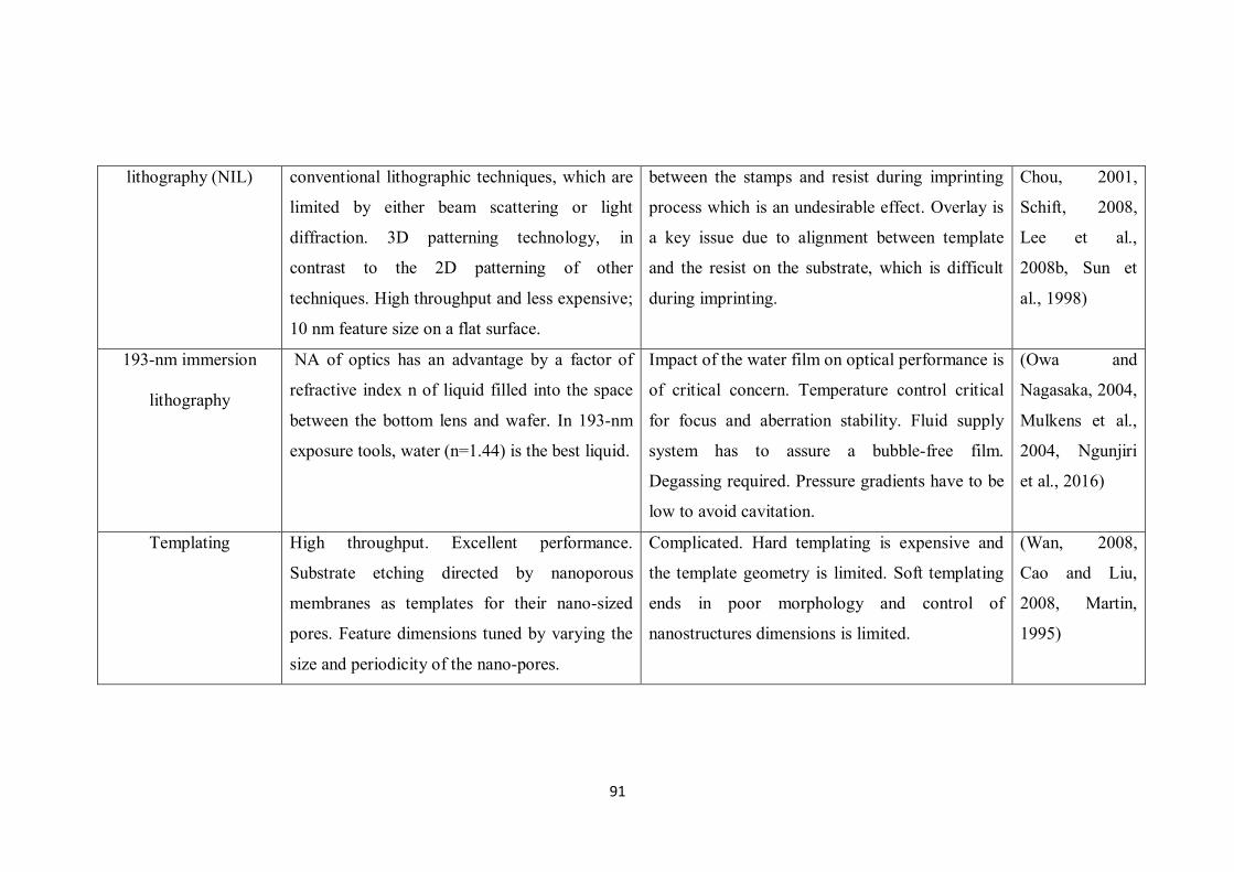
91
lithography (NIL) conventional lithographic techniques, which are
limited by either beam scattering or light
diffraction. 3D patterning technology, in
contrast to the 2D patterning of other
techniques. High throughput and less expensive;
10 nm feature size on a flat surface.
between the stamps and resist during imprinting
process which is an undesirable effect. Overlay is
a key issue due to alignment between template
and the resist on the substrate, which is difficult
during imprinting.
Chou, 2001,
Schift, 2008,
Lee et al.,
2008b, Sun et
al., 1998)
193-nm immersion
lithography
NA of optics has an advantage by a factor of
refractive index n of liquid filled into the space
between the bottom lens and wafer. In 193-nm
exposure tools, water (n=1.44) is the best liquid.
Impact of the water film on optical performance is
of critical concern. Temperature control critical
for focus and aberration stability. Fluid supply
system has to assure a bubble-free film.
Degassing required. Pressure gradients have to be
low to avoid cavitation.
(Owa and
Nagasaka, 2004,
Mulkens et al.,
2004, Ngunjiri
et al., 2016)
Templating High throughput. Excellent performance.
Substrate etching directed by nanoporous
membranes as templates for their nano-sized
pores. Feature dimensions tuned by varying the
size and periodicity of the nano-pores.
Complicated. Hard templating is expensive and
the template geometry is limited. Soft templating
ends in poor morphology and control of
nanostructures dimensions is limited.
(Wan, 2008,
Cao and Liu,
2008, Martin,
1995)

92
Chemical and plasma
etching
Chemical etching is isotropic, inexpensive and
convenient, reliable, high throughput, excellent
selectivity in most cases with respect to both
mask and substrate materials, enhanced
efficiency in use of etchants
No use of liquid chemicals or etchants to
remove materials from the wafer in plasma
etching, generation of only volatile by-products.
In wet etching, the etched feature has curved
walls and width differs from that of resist
opening. Partly used reagent removal raises
environmental issues.
(Liu et al., 2010,
Qian and Shen,
2005, Robbins
and Schwartz,
1959, Li, 2012)
Anodic oxidation Easy and inexpensive, formation of a
homogeneous oxide coating. Applicable on a
large range of metals.
Voltage and temperature control is crucial. An
excess voltage leads to oxide layer cracking.
(Simka et al.,
2013a, Snow et
al., 1995, Kraft
et al., 2003,
Gong et al.,
2001)
Electrospinning Ultra-thin fibres in range of few nanometres
with large surface areas are produced with
superior mechanical properties and easy-to-use.
Nano-fibers have a high surface-to-volume
ratio, malleability to conform to a range of sizes
and shapes. Nano-fiber morphology can be
Design precision is limited, instability of product
morphology and performance.
(Bhardwaj and
Kundu, 2010,
Greiner and
Wendorff, 2007,
Demir et al.,
2002, Liang et
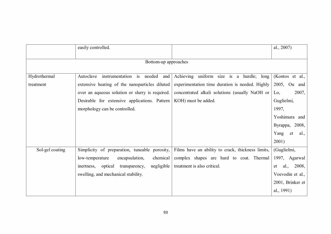
93
easily controlled. al., 2007)
Bottom-up approaches
Hydrothermal
treatment
Autoclave instrumentation is needed and
extensive heating of the nanoparticles diluted
over an aqueous solution or slurry is required.
Desirable for extensive applications. Pattern
morphology can be controlled.
Achieving uniform size is a hurdle; long
experimentation time duration is needed. Highly
concentrated alkali solutions (usually NaOH or
KOH) must be added.
(Kontos et al.,
2005, Ou and
Lo, 2007,
Guglielmi,
1997,
Yoshimura and
Byrappa, 2008,
Yang et al.,
2001)
Sol-gel coating Simplicity of preparation, tuneable porosity,
low-temperature encapsulation, chemical
inertness, optical transparency, negligible
swelling, and mechanical stability.
Films have an ability to crack, thickness limits,
complex shapes are hard to coat. Thermal
treatment is also critical.
(Guglielmi,
1997, Agarwal
et al., 2008,
Voevodin et al.,
2001, Brinker et
al., 1991)

94
Layer-by-layer
assembly
Ease of preparation, versatility, robustness of
products and high throughput. Film thickness is
usually in nanometer scale, and deposition is
controlled by adjusting parameters such as
solution pH, ionic strength, and immersion time.
Lack of precise control and complex in design
and operation.
(Ke et al., 2014,
Lee et al.,
2008a, Jiang
and Tsukruk,
2006, Tang et
al., 2006,
Podsiadlo et al.,
2005, Borges
and Mano,
2014)
Atomic layer
deposition (ALD)
Film thickness depends on reaction cycles,
which makes the thickness control accurate and
simple. High aspect ratio structures,
nanoparticles, nanowires, soft materials and
biological constituents can be coated.
Precursors should have a high vapour pressure to
permit chamber volume saturation upon dosing
and thermal stability to circumvent decomposition
before next step. Certain metals and semi-
conductors such as Si and Ge are difficult to
deposit.
(Leskelä and
Ritala, 2003,
Tynell and
Karppinen,
2014, Marichy
et al., 2012)
Chemical and physical
vapour deposition
Uniform film thickness. Independent from
substrate forms/shapes; high efficiency. Method
is convenient to use and has a high throughput.
PVD is a helpful and promising technique to use
Expensive vacuum components, high-temperature
process.
PVD has a poor adhesion rate due to high internal
stress. Another reason is poor chemical bonding
(Ke et al., 2014,
Umar et al.,
2005, Matsui et
al., 2000,

95
an interface layer with a correct material
combination.
to the substrate.
Mathur et al.,
2004, Kusano et
al., 1998)
*Table contents have been added and updated, with permission from (Biswas et al., 2012).

96
2.5. Applications of nano-structured ‘smart’ surfaces
This section highlights the applications of some nano-structured surfaces towards
relevant biotechnological industries. The surfaces have been aptly named as ‘smart’
surfaces, as they fulfil multi-dimensional roles and their application is not limited
towards a specific direction, they cater to a variety of speciality roles.
2.5.1. Nano-patterned titanium surface as an implant surface
Metallic biomaterials are used for surgical implants due to good formability, high
strength and fracture resistance (Niinomi, 2008, Frosch and Stürmer, 2006). Nano
crystalline metals and their alloys are categorized by their small grain size and high
volume fraction of grain boundaries, giving rise to superior physical, chemical and
mechanical properties as compared to other materials possessing a conventional
grain size (Meyers et al., 2006, Wang et al., 1995, Cavaliere, 2015, Weertman et al.,
1999). The list of metals currently used as a successful implantable surface is limited
to three main groups: iron-chromium-nickel alloys (austenitic stainless steels), cobalt
chromium-based alloys, nickel-titanium (NiTi) alloys and titanium and titanium
alloys (Okazaki and Gotoh, 2005, Matsuno et al., 2001, Eriksson, 1986, Gotman,
1997).

90
When metallic implants are placed in a physiological environment, metal ions are
released in the surrounding areas from the surface, which ultimately lead to implant
failure and removal. Titanium is superior to other implantable metals due to the
development of a stable passive TiO2 layer on its surface which acts as a corrosion
protection layer. This layer is composed of a protective titanium oxide and Ti ions
are the only metal ions that can be released. The release of titanium ions is
favourable in the process of osseo-integration since Ti is intrinsically biocompatible
and often helps in the formation of bone on the implant surface. Titanium and its
alloys also have a lower elastic modulus value (almost two-fold lower compared to
stainless steel and Co–Cr), which results in less stress shielding and associated bone
resorption around Ti orthopaedic and dental implants (Raines et al., 2010, Abron et
al., 2001). Ti–6Al–4V is the most widely used surgical Ti alloy. The addition of
alloying elements, such as aluminium and vanadium also allows for a significant
improvement of the mechanical properties of titanium (Polyakov et al., 2015). Apart
from the elastic and mechanical properties, two conditions are of utmost importance
when fabricating a successful implant surface: greater adsorption of proteins for an
enhanced bone-implant integration and minimal bacterial attachment on the implant
surface. Post-operative implant infections are profoundly influenced by the ability of
the native bacteria and eukaryotic cell lines such as fibroblasts, osteoblasts and
neural cell lines to attach and proliferate on the surface of the biomaterial. The
capability to engineer cell responses on material surfaces is dependent upon gaining
an understanding the role of surface topology towards affecting implant–cell
interactions (Frenkel et al., 2002, Das et al., 2007, Raaif et al., 2007).
Protein attachment on surfaces is a dynamic process in which surface topography is
used as a medium to bind specific proteins from biological fluids. This protein
96

98
uptake may be central in blood contacting and other antifouling applications (Luong-
Van et al., 2013). Upon insertion into the body, the implant surface comes into
contact with blood and its components, such as fibronectin and vitronectin. The
proteins adsorbed on the surface of the implant help to form a supporting matrix for
cell attachment. The cells usually attach to the extracellular matrix with the help of
certain molecules called integrins (Adden et al., 2006, Pettit and Bowie, 1999,
Hallab et al., 2001, MacDonald et al., 1998). Cellular interactions with ECM
molecules are believed to generate specific signals that are transduced through the
integrins to the cytoplasm, the cytoskeleton, and the nucleus (Degasne et al., 1999).
These signals act as cues that aid in cell proliferation and attachment on the surface.
The signals at the nano-bio interface are dependent on topographical such as surface
roughness, angle of curvature, porosity, surface crystallinity, heterogeneity,
roughness, surface wettability, surface free energy, as well as electro-chemical
factors such as Vander-Waal force, electrostatic and steric repulsive forces (Degasne
et al., 1999, Kilpadi et al., 2001, Sano and Shiba, 2003).
Implantation suffers from an additional risk of infections in approximately 1.5–2.5%
of hip and knee arthroplasties, resulting in device failure (Puckett et al., 2010).
Devices that are associated with bacterial infection include non-surgically implanted
devices (contact lenses, endotracheal tubes, and urinary and central venous catheters)
and long-term implanted devices (cardiac valves, vascular grafts, plastic surgery
augmentation devices, and joint replacements). A reduction in the degree of bacterial
attachment on implant surfaces is paramount to avoid subsequent infections arising
from the implantation of biomedical devices. Several approaches have been explored
to address this issue, such as antibiotic therapies, drug delivery methods, and surface
coatings. These practices have not been fully put to use, as their efficacy is not

99
satisfactory over long-term usage. Coatings and devices loaded with time-release
antibiotics deplete over time. Studies report that bacteria develop sustained
resistance to antibiotic treatments and antibacterial coatings and leave the system
ineffective. Therefore, alternative routes to alter the growth of bacterial attachment
have been put into use (Graham and Cady, 2014). These include, but are not limited
to, surface chemistry (functional groups, electrostatic charge, and coatings), surface
energy (as related to the surface hydrophobicity), mechanical properties (elastic
modulus, shear forces), environmental conditions (pH, temperature, nutrient levels
and competing organisms), surface topography, as well as bacterial surface structures
(pili, flagella, fimbriae, adhesins) (Chen et al., 2013). In most of the naturally
occurring instances, surface topography can be accurately monitored at the macro-
scale but is not highly controlled at the micro- and nano-scale. Most bacterial cells
are in the micrometre size range, while their surface appendages are in the nanometre
size range. An accurate control of surface topography in the nanometre to micro-
metre size range has a pivotal role in reducing bacterial attachment and subsequent
biofilm formation upon the metallic substratum.
2.5.2. Use of bactericidal black silicon in microfluidics
With the recent discovery of the mechanical biocidal properties of insect wings
containing a nanostructured array of pillars, the study of surface topography-
mediated bactericidal surfaces has undergone a major transition. Numerous studies
have focused on the manufacture of such surface topographies, and have reported
substrata that perform a dual function of prevention of bacterial attachment followed
by complete elimination. Black silicon (bSi) refers to silicon surfaces covered by a
layer of nano- or micro-structures. These structures suppress reflection, increasing

100
the scattering and absorption of light (Liu et al., 2014b, Jansen et al., 2009, Jansen et
al., 1995). bSi possesses a number of attributes, such as high reflectance, a
chemically active surface area, superhydrophobicity, a high luminescence
competence and a strong bactericidal agent with “self-cleaning” properties when the
topographical dimensions are condensed to a few nanometres. These properties have
enabled bSi to be used in a wide range of applications, such as micro-electro-
mechanical systems (MEMS) (De Boer et al., 2002, Bhardwaj et al., 1997, de Boer et
al., 1995), photonic devices (Jansen et al., 1995, Priolo et al., 2014, Serpenguzel et
al., 2008), drug delivery (Teo et al., 2006, Savin et al., 2015), lithium-ion batteries
(Chan et al., 2009, Dimov et al., 2003, Ruffo et al., 2009), hydrogen production by
photo-electrochemical splitting of water (Oh et al., 2011, Ao et al., 2012, Shen et al.,
2015), and as a bactericidal surface (Hasan and Chatterjee, 2015, Ivanova et al.,
2013a). The nano-pillared substrata border bacterial attachment in a way that the
bacterial cell , upon landing have less contact area between the pillars on the surface
as compared to the non-patterned control surfaces (Hasan et al., 2013a, Armentano et
al., 2014, Rizzello et al., 2013).
Since the 1990s, the area of microfluidics has developed into a multipurpose
technology (Gravesen et al., 1993). While initially focused on flow through simple
channel systems, the recent channel designs have become more complex in nature.
Substantial effort is put into the integration of unit operations on-chip such as sample
pre-treatment, reagent mixing, reaction, and end-product seperation (Moon et al.,
2006, Paegel et al., 2003, Liu et al., 2004, Krulevitch et al., 2002). Many
microfluidic applications are quite cumbersome as they require multiple steps and
trained personnel for successful implementation (Mariella Jr, 2008). A shift to novel
approaches has now been recognized, which target straightforward modifications:

101
application of functionalized coatings, adsorption beads and active substrata (Witters
et al., 2013, Chen and Fair, 2015, Choi et al., 2002, Lahann et al., 2003, Pugmire et
al., 2002, Hu et al., 2004). The reasons for a simplistic approach towards fabricating
such a microfluidic device lies in the fact that it reduces the number of steps
involved and results are relatively easily obtained. The functionality of microfluidic
devices significantly increases if these devices can be combined with photonics-
based devices to create an combined microfluidic photonics, referred to as ‘opto-
fluidics’ (Monat et al., 2007, Fainman et al., 2009, Monat et al., 2008).
Amalgamation of microfluidics with photonics characterizes not only a new
technology stage but also a conversion to the new prototype of bio-system-on-a-chip
(BSoC) (Ducrée et al., 2007, Oosterbroek and Van den Berg, 2003, Tamanaha et al.,
2002). Techniques such as fluorescence resonance energy transfer (FRET), optical
scattering, and surface-enhanced Raman spectroscopy (SERS) are some of the most
accurate methods to identify analytes at both the cellular and molecular level (Mere
et al., 1999, Hsieh et al., 2009, Benz et al., 2013, Godin et al., 2008). Black silicon is
one such substrate, which has been recently combined with microfluidics to trace
bacteria using SERS (Hartley et al., 2015). Combination of the nano-structured
bactericidal black silicon surface with a simple microfluidic channel design can be
used to remove bacterial cells from real-time samples such as blood, urine and
commercially available water samples. The bacterial cells could be easily detected
and killed, with the device being able to be re-used and up-scaled for industry
applications.

102
2.5.3. Use of electro-active bacteria towards designing a microbial
fuel cell (MFC)
Redox PVA based hydrogels are being considered for use in microbial and
enzymatic fuel cells (Nakahata et al., 2011, Heller, 2006). These three-dimensional
polymeric systems provide an extracellular, matrix-like environment that is
compatible with cell viability leading to increased bio-electrode efficiency. Redox
polymers often contain mediators, which are “wired” into the cross-linked polymer
network (Heller, 2004). Compounds such as osmium and ferrocene-based mediators
are commonly as they own flexible chains which help in increased electron transfer
from enzyme to the mediator (Meredith and Minteer, 2012, Cooney et al., 2008,
Calabrese Barton et al., 2004). However, one challenge to be addressed in biofuel
cell design is low power density, which is due to low current density (Bartona and
Atanassov, 2004, Vielstich et al., 2009). One reason for this phenomenon is that only
a small amount of enzyme is effectively used in the electrode reactions (Tamaki and
Yamaguchi, 2006). This happens as adequate electrons are not involved in the
catalytic reaction to increase the power efficiency. To overcome this shortcoming,
electro-conducting bacterial cells have been coupled within the three-dimensional
network to help increase the flow of electrons within the polymeric mesh and
increase the power density of the fuel cell (Reshetilov et al., 2006). Electro
conductive bacteria such as Shewanella ,Geobacter spp., Gluconobacter spp. have
been studied and found to transfer respiratory electrons to the bio-electrodes via
outer membrane c-type cytochromes (c-Cyts) (Lin et al., 2012, Richardson, 2000,
McMillan et al., 2013, Busalmen et al., 2008). Three strategies for extracellular
electron transfer have been reported in detail explaining how different metal-
reducing bacteria are able to respire insoluble substrates; direct electron transfer

103
upon which the active centre of the membrane enzyme is directly connected to the
electrode, formation of nano-wires via 2-3 µm long pili and fimbriae, and thirdly via
mediated electron transfer by adding certain redox mediators, which are able to
transfer electrons effectively (Reguera et al., 2005, Bücking et al., 2012, Rosenbaum
et al., 2011, Kotloski and Gralnick, 2013). The two most commonly studied bacterial
model systems in this regard are Geobacter sulfurreducens and Shewanella
oneidensis strain MR-1. While they both use an assortment of multiheme c-type
cytochromes, only Shewanella bacteria breathes insoluble substrates without having
any form of direct contact (Lies et al., 2005, Nevin and Lovley, 2000). These
bacterial strains can generate conductive “nanowires” via pili-like structures
enabling the respiration of insoluble substrates (Gorby et al., 2009, Reguera et al.,
2005). Unlike Geobacter, Shewanella cultures can accumulate riboflavin (B2) and
flavin mononucleotide (FMN) in supernatants, which can act as electron shuttles to
accelerate reduction of insoluble substrates (Schaetzle et al., 2008). The metal-
reducing aptitude of Shewanella is due to a set of surface-associated Mtr/Omc
proteins plus three additional outer membrane decaheme c-type cytochromes, two
periplasmic decaheme cytochromes (MtrA and MtrD), and two outer membrane non-
cytochrome proteins (MtrB, MtrE) (Fuller et al., 2014, Von Canstein et al., 2008).
These proteins have a collaborative function to relay electrons out of the cell outer
membrane (Wang et al., 2011a). Alternatively, Geobacter spp. are also known to not
require exogenous mediator addition and are able to oxidize a large variety of anoxic
wastes to form carbon dioxide (Holmes et al., 2006). This mechanism eases the
process of quantitative direct electron transfer to electrodes.
This study shows that non-motile Gluconobacter spp have the ability to transfer
electrons by forming self-aligned ‘biowires’ by disrupting an immobilized polymer

104
network, which are able to transfer the electrons onto a bio-anode system. This leads
to a three-dimensional environment that enhances electron transfer via extracellular
electron transfer by disrupting the porous structure of the polymer mesh. The PVA-
VP hydrogel acts as not only as a cyto-compatible cellular network for impulsive
encapsulation of bacteria, but also as a mediator of electron transfer between the
bacteria and the surface of bio-electrodes. One of the studies in this thesis has looked
into the likelihood of constructing a cell-based device with this hydrogel/bacteria
hybrid biomaterial by examining the hydrogel formation, bacteria encapsulation,
bacterial viability and proliferation rate, and the related electrochemical properties. It
is assumed that this optimized three-dimensional PVA-VP hydrogel/ bacteria
network will provide valuable and significant progress in the preparation of
microbial fuel cells.

105
Chapter 3
Materials & Methods

106
3.1 Overview
This chapter focusses experimentally on the chemical and structural characterisations
as well as the biological activity and physical surface properties of the
nanostructured surfaces. Additionally, experiments that attempt to model how these
surface structures are generated are used to explore the mechanisms involved in their
biological activities.
3.2. Materials
Commercially pure ASTM Grade-2 titanium round Bar, 10-of 1/2" diameter x
200mm long was purchased from VDM Metals Australia Pty Ltd and was later cut in
billets 10 mm in diameter and 35 mm in length, with an average grain size of 4.5
µm. Potassium hydroxide ACS reagent, ≥ 85%, pellets (KOH) was procured from
Sigma-Aldrich. A p-type boron-doped 100 mm diameter commercial Si wafer with
specific resistivity of 10-20 Ω cm-1, (100) oriented surface and 525 ± 25 μm
thickness was obtained from Atecom Ltd (Taipei, Taiwan). SYLGARD® 184
SILICONE ELASTOMER KIT was purchased from Dow Corning. Oxygen asher
was purchased from EMITECH. Hot air oven used to bond the microfluidic channel
was purchased from Laboratory equipment pty ltd. A four channel peristaltic pump
was procured from John Morris Scientific Pty Ltd. Pump silicon 2-stop tubings with
an internal diameter of 1.65 mm were purchased from ANALYTICAL WEST INC.
Poly (vinyl alcohol) (PVA) with average molecular weights of 67 kDa and 125 kDa
respectively were purchased from Sigma-Aldrich. N-vinyl pyrrolidone (N-VP)
containing sodium hydroxide as inhibitor, ≥ 99% (C6H9NO) and ammonium cerium
(IV) nitrate (Ce (NH4)2(NO3)6) were supplied by Sigma-Aldrich. All chemicals were
of analytical and high-performance liquid chromatography (HPLC) grade. Milli-Q

107
water was used for the fabrication of hydrogels as well as for the swelling ratio
analysis. Adhesive tape (ARclad® IS-8026 Adhesives Research, Inc.) was used to
join the channel sides together (Gervinskas et al., 2011, Ivanova et al., 2012b), as it
has been found to be suitable for experiments conducted over a wide range of
temperatures.
3.3. Surface fabrication
3.3.1 Nano-patterned titanium
Commercially pure ASTM Grade-2 titanium, in billets 10 mm in diameter and 35
mm in length, with an average grain size of 4.5 µm were used in this study. Small
disc-shaped specimens were prepared from the as-received titanium rods and were
subjected to further hydrothermal treatment to form nano-wired structures on their
top surfaces. The titanium control samples were prepared by progressively grinding
their surface using silicon carbide grinding papers. This was to ensure a substrate
could be obtained that contained a regular plane surface with slight shallow
scratches, free of deformation pits. Hydrothermal treatment of the as-received
titanium billets was performed by fully immersing the billets in 10 M KOH solution
in a glass container and subjecting them to a high temperature and pressure
treatments in a steel autoclave. The temperature and the pressure were 121 ºC and
10–15 psi, respectively. The liquid hydrothermal process was performed for a one-
hour period. The billets were subjected to an additional heat-treatment procedure in
a hot air furnace at 400 ºC for 3 h. As a final cleaning step for the AR-Ti and HTE-Ti
samples, the substrates were rinsed and ultrasonically cleaned, firstly in acetone,
ethanol and finally in MilliQ Water (with a resistivity of 18.2 MΩ cm-1) to remove
any trace impurities.

108
3.3.2. Black silicon surfaces
Reactive ion etching (RIE) with SF6 and O2 was performed for 5 minutes to produce
the nano-pillars on silicon wafers using an Oxford PlasmaLab 100 ICP380
instrument. A p-type boron-doped 100 mm diameter commercial Si wafer with
specific resistivity of 10-20 Ω cm-1, <100> oriented surface and 525 ± 25 µm
thickness (Atecom Ltd, Taiwan) was used as a substrate for the bSi formation. RIE
processing was mixed mode with etching and passivation occurring simultaneously
under the following conditions: SF6 gas flow rate of 65 sccm, O2 gas flow rate of 44
sccm, a pressure of 35 mTorr, 100 W RIE power, 20° C electrode temperature and
10 Torr He backside cooling pressure (Gervinskas et al., 2013, Žukauskas et al.,
2013).
3.3.3. bSi integrated in a microfluidic channel
The microfluidic chip was assembled via a simple method using an adhesive tape
spacer, which allowed the shape and height of the microfluidic channel to be
defined. In such a design, an adhesive double sided tape (ARclad IS-8026-15,
Adhesives Research Inc.) was placed on the glass substratum with the channel layout
being defined by a laser cutter (CO2 laser VLS 2.30, Versa Laser). It was completed
by placing the top plate of bSi and sealed with silicone. The tubing, obtained from
syringe needles, was added and sealed in position, as required. In this study, bSi was
used as the top lid of the flow chamber, which was laser cut (Pharos, Light
Conversion) out of a 0.4 mm-thick bSi wafer. The channel height was determined by
the thickness of the adhesive tape at 15 µm. This channel height is several times
larger than the size of the rod-shaped P. aeruginosa cells, which had dimensions of
approximately 2 × 1 µm2 (Vallet-Gely and Boccard, 2013).
109
3.3.4. Hydrogel thin films
Aqueous PVA solution (5 wt. %) was prepared by dissolving PVA in Milli-Q water
at 80 ºC under constant magnetic stirring. The solution was then subsequently cooled
down to room temperature. An appropriate weight of N-vinyl pyrrolidone (VP)
monomer (0.1 ml) was added into the PVA solution under magnetic stirring at a
maintained temperature of 40 ºC. Ceric ammonium nitrate (CAN) was added as an
initiator (0.8 ml) of the free-radicle polymerization reaction. The entire system was
purged continuously with N2 gas for three hours to remove the presence of any
oxygen bubbles. The resulting homogenous polymer solutions so formed were cast
on a glass side (76mm × 26mm × 1mm) for further chemical and mechanical
characterizations. Aqueous solution of ammonium cerium (IV) nitrate
(NH4)2Ce(NO3)6 and N-vinylpyrrolidone (0.1 ml) were added to aqueous solutions
of PVA (20 ml, 5% w/v) with stirring at 400 ºC. The nitrogen gas was passed
through the solutions for 3 h to remove the dissolved oxygen. The resultant hydrogel
was used as a matrix for the immobilization of the microorganisms.
3.4. Surface characterization
3.4.1. Scanning Electron Microscopy (SEM)
Samples were first coated with a thin layer of gold film (~ 3 -5 nm thickness) using a
Dynavac CS300. The high-resolution scanning electron microscopy images were
obtained using field emission SEM (FESEM, SUPRA 40VP) at 3kV under 15,000×
and 35,000× magnification (Nguyen et al., 2015b).

110
3.4.2. Optical profilometry
The surface topography of the substrates was analyzed using the Wyko NT1100
(Veeco Instruments, Bruker) optical profiling system in the white light vertical
scanning interferometry mode using a 50× objective lens. Three samples of each
surface type were briefly scanned to evaluate the overall homogeneity of the surface
and then the topographical profiles were studied in detail at five different locations.
Vision 64 software was used to analyse the surface roughness profiles of the
substrates. In order to analyse the surface topography, different surface roughness
parameters were employed: the average roughness (Sa), root-mean square (rms)
roughness (Rq) and maximum peak height (Smax) were performed using Gwyddion
data processing software (Nečas and Klapetek, 2012). Two additional parameters,
skewness (Ssk) and kurtosis (Sku), which describe surface morphology, have also
been utilised. Skewness measures the symmetry of the height probability density
function and kurtosis measures profile ‘peakedness’ (Kim, 2013, Yeau-Hen, 1998,
Dong et al., 1992, Nguyen et al., 2013b).
3.4.3. Atomic Force Microscopy (AFM)
Atomic force microscope (Innova, Veeco, USA) in tapping mode was employed to
examine the surface topographic profiles. Phosphorus-doped silicon probes (MPP-
31120-10, Veeco) with a spring constant of 0.9 N m-1, radius of curvature (tip) of 8
nm and a resonance frequency of approximately 20 kHz were utilised for surface
imaging. Scanning was carried out at a right angle to the axis of the cantilever at 1
Hz. The topographical data of the investigated surfaces were processed with first
order horizontal and vertical levelling. In order to analyse the surface topography,
different surface roughness parameters were employed: the average roughness (Ra),
111
root-mean square (rms) roughness (Rq) and maximum peak height (Rmax) were
performed using Gwyddion data processing software (Nečas and Klapetek, 2012).
Two additional parameters, skewness (Rsk) and kurtosis (Rku), which are useful for
describing surface morphology, have also been utilised (Gadelmawla et al., 2002,
Lamolle et al., 2009, Truong et al., 2009, Al-Kindi and Shirinzadeh, 2007, Truong et
al., 2010). Bearing statistics, including peak height (Rpk), valley depth (Rvk), core
roughness (Rk) and Rm were also analysed, as described elsewhere (Crawford et al.,
2012). These were able to distinguish the differences between surfaces with similar
average roughness. All images were produced using an Innova atomic force
microscope (Veeco) and the raw data was then extracted to the Gwyddion software
for processing (Nečas and Klapetek, 2012).
3.4.4. X-Ray Diffraction (XRD)
The presence of crystalline peaks of Titanium oxide after chemical treatment of the
titanium samples was analysed by the usage of an X-ray diffractometer (XRD,
PANalytical X’Pert with Cu Ka radiation) with Ѳ=20º to 80º. The titanium samples
were mounted on metallic holders and were attached onto the holders with the help
of a thin layer of sticky tape. The peaks were analysed though Bragg’s law, which is
one of the most important aspects of XRD. The equation is
nλ=2dsinθ. (3.1)
Where
n is an integer, λ is the wavelength in nm, d is the inner spacing, and theta (θ) is the
angles of the diffractions. This equation is used to create a graph that plots the angles
to find intensity.

112
3.4.5. X-ray Photoelectron Spectroscopy (XPS)
A VG ESCALAB 220i-XL X-ray Photoelectron Spectrometer equipped with a
hemispherical analyser was used for XPS data acquisition. Samples underwent
alternating data acquisition and ion beam etching cycles. Monochromatic Al Kα X-
rays (1486.6 eV) at 220 W (22 mA and 10 kV) were used as incident radiation for
data acquisition. Survey scans were carried out at pass energies of 100 eV over a
binding energy range of 1200 eV. Base pressure in the analysis chamber was below
7.0 × 10⁻⁹ mbar and during sample depth profile analysis rose to 1.5 × 10⁻⁷ mbar. Ion
beam etching was performed using a 4 keV Argon beam over a 2 mm × 2 mm area
for intervals of 120 seconds. Data acquisition and etching was performed for 5
cycles, with a total etching time of 3000 seconds. XPS data were fitted using mixed
Gaussian Lorentzian peak shape and linear background subtraction with Casa XPS.
3.4.6. Synchrotron Radiation Fourier Transform Infrared
spectroscopy (SRFTIR)
3.4.6.1. FTIR in attenuated total reflection (ATR) mode
The infrared beam passes through the ATR crystal and reflects back, producing an
evanescent wave, which penetrates no more than a few micrometres into the upper
surface of the sample (in this case ~1 µm). This method provides information on the
chemical functionality of the surface in contact with the crystal. The ATR
measurements of the hydrogel samples with and without the bacterial cells were
made with a hemispherical ATR element (germanium and zinc selenide (ZnSe)) with
the flat side of the hemisphere pressed into contact with the sample (Beaussart et al.,

113
2012, Beattie et al., 2012). Similar with FTIR in transmission mode, the data was
analysed using OPUS version 6.5 software.
3.4.7. Wettability
The contact angles of Milli-Q water on both biological and synthetic surfaces was
measured using the sessile drop method (Crawford et al., 1987, Lander et al., 1993,
Öner and McCarthy, 2000, Van Oss et al., 1988, Guy et al., 1996). The contact angle
measurements were carried out in air using an FTA1000 (First Ten Ångstroms, Inc.,
Portsmouth, VA, USA) instrument. An average of at least ten measurements was
obtained for each sample, in duplicate. The evaluation of contact angles was
performed by recording 50 images in 2 seconds with a Pelcomodel PCHM 575–4
camera using FTA Windows Mode 4 software. All measurements were taken at
ambient conditions of 21ºC and relative humidity of 60-70 %.
3.5. Bacterial strains and growth conditions
Pseudomonas aeruginosa ATCC 9027, Staphylococcus aureus CIP 65.8T,
Escherichia coli K 12 and Gluconobacter oxydans subsp. industrious 1280 were
used in this study. The bacterial strains were obtained from The Collection of Institut
Pasteur (Paris, France), American Type Culture Collection (Manassas, VA, USA).
Prior to individual experiments, bacterial cultures were refreshed from stock onto
nutrient agar (BD, Franklin Lakes, NJ, USA). For individual experiments, bacterial
cell suspensions of each strain were prepared in 5 mL nutrient broth (BD, Franklin
Lakes, NJ, USA) from fresh culture grown overnight in an incubator at 37 °C.
Bacterial cells were collected at the logarithmic stage of growth and the suspensions
were adjusted to OD600 = 0.1. The nano-structured surfaces were then immersed in
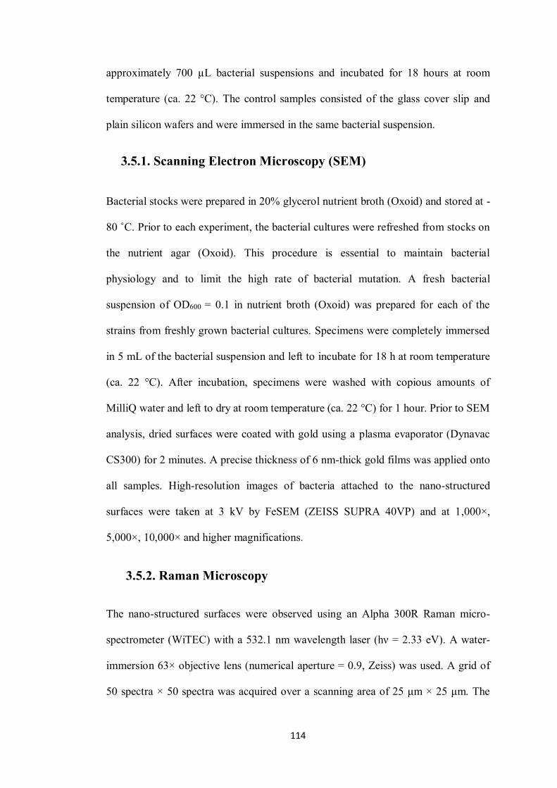
114
approximately 700 µL bacterial suspensions and incubated for 18 hours at room
temperature (ca. 22 °C). The control samples consisted of the glass cover slip and
plain silicon wafers and were immersed in the same bacterial suspension.
3.5.1. Scanning Electron Microscopy (SEM)
Bacterial stocks were prepared in 20% glycerol nutrient broth (Oxoid) and stored at -
80 ˚C. Prior to each experiment, the bacterial cultures were refreshed from stocks on
the nutrient agar (Oxoid). This procedure is essential to maintain bacterial
physiology and to limit the high rate of bacterial mutation. A fresh bacterial
suspension of OD600 = 0.1 in nutrient broth (Oxoid) was prepared for each of the
strains from freshly grown bacterial cultures. Specimens were completely immersed
in 5 mL of the bacterial suspension and left to incubate for 18 h at room temperature
(ca. 22 °C). After incubation, specimens were washed with copious amounts of
MilliQ water and left to dry at room temperature (ca. 22 °C) for 1 hour. Prior to SEM
analysis, dried surfaces were coated with gold using a plasma evaporator (Dynavac
CS300) for 2 minutes. A precise thickness of 6 nm-thick gold films was applied onto
all samples. High-resolution images of bacteria attached to the nano-structured
surfaces were taken at 3 kV by FeSEM (ZEISS SUPRA 40VP) and at 1,000×,
5,000×, 10,000× and higher magnifications.
3.5.2. Raman Microscopy
The nano-structured surfaces were observed using an Alpha 300R Raman micro-
spectrometer (WiTEC) with a 532.1 nm wavelength laser (hν = 2.33 eV). A water-
immersion 63× objective lens (numerical aperture = 0.9, Zeiss) was used. A grid of
50 spectra × 50 spectra was acquired over a scanning area of 25 μm × 25 μm. The

115
integration time for each spectrum was 1 second. Independent scanning was repeated
twice on each of the two different samples. The signal was collected at an angle of
90° relative to the sample plane.
3.5.3 Bacterial viability assays
Viability assays were performed by standard plate counts (Postgate, 1969). P.
aeruginosa and S. aureus cells and E. coli were suspended in 5 mL of phosphate
buffered saline (PBS) and adjusted to OD600 = 0.1. Re-suspended cells were diluted
1:10 and then incubated in 3.5 cm diameter wells, in triplicate, with each well
containing a 1 cm2 area substrate sample of a black silicon and a smooth silicon
wafer. The cell suspensions were then sampled (100 µL) at discrete time intervals (3
hours and 18 hours), serially diluted 1:10 and each dilution spread on three nutrient
agar plates. Resulting colonies were then counted and the number of colony forming
units per mL was calculated. The number of colony forming units was assumed to be
equivalent to the number of live cells in suspension (Postgate, 1969). The maximum
bactericidal efficiency was measured as the number of inactivated cells per square
centimetre of sample per minute of incubation time, relative to the control surfaces.
3.5.4. Confocal Laser Scanning Microscopy (CLSM)
Confocal laser scanning microscopy was used to visualise the proportions of live
cells and dead cells using a LIVE/DEAD® BacLight™ Bacterial Viability Kit,
L7012. SYTO® 9 permeated both intact and damaged membranes of the cells,
binding to nucleic acids and fluorescing green when excited by a 485 nm wavelength
laser. Propidium Iodide only entered the cells that had sustained significant
membrane damage (and therefore considered to be non-viable) and bound with
higher affinity to the intracellular nucleic acids than the SYTO® 9. Bacterial

116
suspensions were stained according to the manufacturer’s protocol and imaged using
a Fluoview FV10i inverted microscope (Olympus, Tokyo, Japan) (Ivanova et al.,
2013a).
3.5.5 Statistical analysis
The results obtained were expressed in terms of their mean values and the
corresponding standard deviations following commonly used protocols. Statistical
data processing was performed using paired Student’s two-tailed t-tests to evaluate
the consistency of results (asterisked if p < 0.05) in figures and tables.
3.6. Eukaryotic cell growth conditions
The culturing of primary human fibroblasts (pHF) on Ti surfaces was performed
according to the methods described in the approved Biosafety Project 2014/SBC01.
The culture medium (Promocell) was supplemented with 2% fetal bovine serum
(FBS), fibroblast growth factors (1 ng/mL) and insulin (5 μg/mL). Cells were
cultured to 70–80% confluence and were then trypsinized using the Detach kit
(Promocell). The AR-Ti and HTE-Ti samples were seeded with pHF at a density of
105 cells per cm2 for each independent experiment. After 1, 3 and 10 days’
incubation periods, the control and titanium surfaces were gently washed with PBS,
fixed with 4% p-formaldehyde for 15 minutes, permeabilized in 0.1% Triton X for 5
minutes then blocked with 1% BSA for 60 minutes. Image-IT® FX Signal Enhancer
(Invitrogen) was also used during the fixation stage to enhance the fluorescent
signals. Any fixed cells present on the substrate surfaces were treated with a primary
anti-vinculin antibody (Sigma) overnight, followed by goat anti-mouse secondary
antibody conjugated with Alexa Fluor 594 (Invitrogen). Actin filaments were
visualized by staining the cells with Alexa Fluor 488 conjugated Phalloidin

117
(Invitrogen). Cell nuclei were labeled using DAPI (Invitrogen). Samples with stained
cells were then placed in a μ -Disc 35 mm culture disc (ibidi GmbH, Martinsried,
Germany) for imaging in a Fluoview FV10i inverted microscope (Olympus, Tokyo,
Japan). After incubation, all samples were washed with 10 mM PBS and fixed in
2.5% glutaraldehyde (Sigma) for 30 min, then gently washed with of 10 mM PBS
and progressively dehydrated in graded ethanol solutions (30, 50, 70, 90 and 100%
v/v). The ZEISS SUPRA 40VP field-emission scanning electron microscope (Carl
Zeiss NTS GmbH, Oberkochen, BW, Germany), operated at 3 kV, was used to
determine the attachment and proliferation of cells on the substrate surfaces.

118
Chapter 4
Fabrication and investigation of
antibacterial efficiency of bio-mimicked, nano-
patterned arrays on titanium

119
4.1. Overview This chapter introduces the concept of modifying titanium surfaces to mimic
naturally occurring surfaces found in nature. In most cases, these surfaces contain
nano-arrays of pillars that can potentially exhibit antibacterial properties. Major
sources of inspiration for this work have been obtained from studying the surfaces
of dragonfly wings, which possess antibacterial characteristics (Ivanova et al.,
2013a, Nowlin et al., 2015, Webb et al., 2014, Nguyen et al., 2015a). Titanium and
its alloys remain the most popular choice as a medical implant material because of
their desirable properties such as inertness, light weight, high compressive yield
stress and its ability to integrate with human tissue, amongst others (Özcan and
Hämmerle, 2012, Yan Guo et al., 2012, Mishnaevsky et al., 2014, Rani et al., 2009,
Semlitsch et al., 1985, Davidson and Kovacs, 1992, Crawford et al., 2007). The
successful osseo integration of titanium implants is, however, adversely affected by
the presence of bacterial biofilms that can form on the surface. Hence, identification
of methods for preventing the formation of bacterial biofilms on titanium surfaces
has been the subject of intensive research over the past few years (Neoh et al., 2012,
Tesmer et al., 2009, Mombelli et al., 1988, TAKANASHI et al., 2004, Dong et al.,
2007, Fadeeva et al., 2011, Scarano et al., 2004). In this study, the surface of
titanium is modified to contain a nano-pillar array through a simple hydrothermal
etching process. The response of these nano-arrays towards the reduction of
bacterial colonization and promotion of growth of human tissue is reported in the
subsequent chapter.
The modification of the commercially pure (CP) grade 2 Ti through liquid
hydrothermal treatment resulted in the formation of micro- and nano-scale features,
with 100 – 200 nm-scale undulations. The as-received (AR-Ti) and hydrothermally

120
etched (HTE-Ti) titanium surfaces were chemically and physically characterized
using X-ray photoelectron spectroscopy, scanning electron microscopy, contact
angle goniometry and optical profilometry, in order to understand the roles that
physical and chemical modification of the surfaces plays in the attachment of
Pseudomonas aeruginosa ATCC 9027 and Staphylococcus aureus CIP 65.8T
bacteria.
These fabricated titanium surfaces were shown to possess selective bactericidal
activity, eliminating almost 20% of the S. aureus and 50% of the P. aeruginosa cells
coming into contact with the surface. These antibacterial surfaces, which are capable
of exhibiting differential responses to bacterial and eukaryotic cells, represent
surfaces that have excellent prospects for biomedical applications.
4.2. Mimicking of dragonfly wing nano-arrays on titanium surfaces
4.2.1. Hydrothermal treatment of titanium surfaces
Commercially pure American Society for Testing of Materials (ASTM) Grade-2
titanium, in billets of 10 mm in diameter and 35 mm in length, with an average grain
size of 4.5 µm was used as sample in this study. Small disc-shaped specimens were
prepared from the as-received titanium rods and were subjected to further
hydrothermal treatment to form nano-wired structures on their top surfaces as shown
in Figure 4.1. The titanium control samples were prepared by progressively grinding
their surface using silicon carbide grinding papers. This was to ensure that the
substrate could be obtained that contained a regular plane surface with slight shallow
scratches, free of deformation pits. Hydrothermal treatment of the as-received
titanium billets was performed by fully immersing the billets in 10 M KOH solution
in a glass container and subjecting them to high temperature and pressure treatments

121
in a steel autoclave. The temperature and pressure were 121º C and 10–15 psi,
respectively. The liquid hydrothermal process was performed for a one-hour period.
The billets were subjected to an additional heat treatment procedure in a hot air
furnace at 400º C for 3 h. As a final cleaning step for the AR-Ti and HTE-Ti
samples, the substrates were rinsed and ultrasonically cleaned, firstly in acetone,
ethanol and finally in MilliQ H2O to remove any trace impurities. The resulting
hierarchical TiO2 nano-wire arrays on the titanium substrates were synthesized via a
single-step hydrothermal growth process. K2Ti2O4(OH)2 nano-wire arrays were
prepared using as-received titanium surface through an alkali hydrothermal process,
then calcined at 400ºC to form potassium titanate (K2Ti6O13) and anatase (TiO2)
through the following chemical reaction:
8TiO2 + 2KOH K2Ti8O17 + H2O (4.1)
K2Ti8O17 K2Ti6O13 + 2TiO2 (4.2) 400 C

122
Figure 4.1. Schematic of liquid hydrothermal treatment process used to fabricate nano-wire arrays on titanium surfaces.
4.2.1.1. Physical changes in the surface topography
Micro- to nano-scale patterning of metallic substrates has been proven as an effective
way by which cell-substrate interactions can be controlled for both prokaryotic and
eukaryotic cells (Anselme et al., 2010, Seddiki et al., 2014, Messina, 2014). The data
pertaining to the topographic and physicochemical characterization of both the AR-
Ti and HTE-Ti titanium surfaces after being subjected to hydrothermal etching
process are presented in Figure 4.2. An optical profilometer was used to provide an
overview of the height of the surfaces as a function of distance over large scanning
areas (Figure 4.2 (A)). Scanning areas of 46.7 µm × 62.3 µm were visualized for
500nm
Furnace at 4000 C
Etched Ti sample
Hydrothermal etching
Aqueous solution of a strong
base

123
each titanium sample, which was also visualized in three-dimensions. The SEM
micrographs revealed that the surface topography was not altered by the
hydrothermal etching on the micron scale, however nano-pillar arrays were observed
to form on the nano-sized features of the AR-Ti (Figure 4.2 (B)). A comparative
roughness analysis was performed using the two conventional surface roughness
parameters, the average roughness (Sa) and the root mean square roughness (Sq).
These parameters showed that the nano-roughness of the HTE-Ti (Sa 401.4 nm) was
greater than that of the AR-Ti (Sa 356.9 nm) due to the presence of the nanowire
arrays. These arrays were found to orient themselves in a perpendicular
configuration to each other, as shown in Figure 4.3. The average size of the
nanowires was estimated to be approximately 40.2 nm. Wettability studies of the
AR-Ti and HTE-Ti surfaces revealed that the HTE-Ti surface was moderately more
than that of the AR-Ti, exhibiting water contact angles (θW) of 73º and 33º,
respectively. Surface wettability is an important parameter that can be used to
indicate the potency of a surface as an antibacterial agent, since many
superhydrophobic surfaces have been shown to exhibit antibacterial behaviour. The
greater water contact angle on the HTE-Ti surface can be attributed to air the
entrapment of air in the interstices between the nano-wires on the surface (Ha et al.,
2014, Chaurey et al., 2012)

124
Figure 4.2. Surface characterization of AR-Ti and HTE-Ti surfaces. (A) High resolution optical profilometry images of AR-Ti and HTE-Ti surfaces on a scanning area of 46.7 µm × 62.3 µm, along with height profiles, indicating the presence of sharp nanowires on the surface of the HTE-Ti. (B) SEM images of AR-Ti and HTE-Ti samples. Scale bar is 400 nm. (C) Graphical illustration of water contact angles of AR-Ti and HTE-Ti surfaces.

125
Figure 4.3. Regularity of the nano-wire arrays on HTE-Ti surface as analysed using Image J. (A) SEM micrographs were altered and filtered to analyse the size and angle orientation of the nano-wire arrays. (B) Size distribution (left) and orientation angle (right) of the nano-wires.
4.2.1.2. Chemical changes in surface topography
The chemical characteristics of the AR-Ti and HTE-Ti substrates are shown in
Figure 4.4 and Table 4.1. X-ray diffractograms demonstrated that no clear difference
existed between the crystalline phases of the AR-Ti and HTE-Ti, however an
enhanced formation of crystalline titanium dioxide on the HTE-Ti was noted, with
an increased ratio being observed between the 2θ peaks of the anatase phase of
titanium dioxide (40º) and the alpha phase of titanium (38º) (Figure 4.4 (A)). High
resolution XPS analysis indicated the presence of high levels of elemental potassium
on the HTE-Ti surface, which likely resulted from the KOH solution used in the

126
etching process. The high-resolution 2p Ti spectra confirmed the formation of
titanium dioxide nanowires on the substrate surface, resulting from the hydrothermal
etching process (Figure 4.4 (B)). No significant difference was observed between the
chemical properties of the AR-Ti and HTE-Ti surfaces. An advantage of using such
a hydrothermal etching technique is that the surface morphology can be readily
controlled by adjusting the parameters of the etching process, which can be
performed without significantly changing the surface chemistry (Aphairaj et al.,
2014, Hamilton et al., 2010b)
Table 4.1. Elemental analysis of AR-Ti and HTE-Ti surfaces.
Element Peak (s) AR-Ti (A %) HTE-Ti (A %) Ti 2p 27.4 23.2 O 1s 66.8 64.2 C 1s 3.9 5.8 Ca 2p 1.6 3.0 K 2p 0.2 3.8

127
Figure 4.4. Chemical elemental analysis of AR-Ti and HTE-Ti substrates. (A) High-resolution XPS spectra of titanium reveal the oxidation states of titanium present on the AR-Ti and HTE-Ti surfaces. (B) X-ray diffraction depicting crystallinity of titanium and titanium dioxide on AR-Ti and HTE-Ti surfaces (alpha (α) phase of titanium, anatase (A) and the rutile (R) phases of titanium dioxide).

128
4.3. Selective bactericidal activity of titanium nano-arrays
The bacterial attachment patterns of two common human pathogens, P. aeruginosa
and S. aureus are presented in Figure 4.5. Representative SEM images were used to
illustrate the bacterial attachment patterns onto the AR-Ti and HTE-Ti surfaces.
These images revealed that bacterial attachment occurred to a greater extent on the
AR-Ti (Table 4.2), with 6.3 ± 2.1 × 10⁴ and 5.2 ± 0.9 ×10⁴ P. aeruginosa cells and
42.4 ± 4.9 × 10⁴ and 37.3 ±3.8 ×10⁴ S. aureus cells attaching to the AR-Ti and HTE-
Ti per mm2, respectively. The bacterial attachments have shown a decrease by 12 %
for S. aureus and 17 % for P. aeruginosa on the treated samples. The total number of
cells attaching to the Ti substrates was consistent with that reported previously
(Loesberg et al., 2007).
Table 4.2. Attachment of bacterial cells on AR-Ti and HTE-Ti surfaces.
The number of viable and non-viable bacterial cells on the substrates was determined
using confocal microscopy. Viable cells were stained green with SYTO 9® and non-
viable cells were stained red with Propidium Iodide (Figure 4.5). The confocal
images demonstrated that 90.4% of the P. aeruginosa and 93.4% of the S. aureus
cells remained viable after attachment to the AR-Ti surfaces, displaying similar
attachment behaviour to that previously reported (Furuhashi et al., 2012, Im et al.,
2012, Neoh et al., 2012). By contrast, 52.9% of the P. aeruginosa and 80.2% of the
S. aureus cells were found to be viable after attachment to the HTE-Ti surfaces. As
Substrate × 104 attached cells/ mm2
S. aureus P. aeruginosa
AR-Ti 42.4 ± 4.9 6.3 ± 2.1
HTE-Ti 37.3 ± 17.2 5.2 ± 0.9
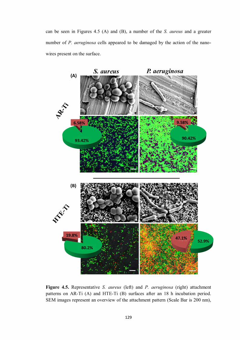
129
can be seen in Figures 4.5 (A) and (B), a number of the S. aureus and a greater
number of P. aeruginosa cells appeared to be damaged by the action of the nano-
wires present on the surface.
Figure 4.5. Representative S. aureus (left) and P. aeruginosa (right) attachment patterns on AR-Ti (A) and HTE-Ti (B) surfaces after an 18 h incubation period. SEM images represent an overview of the attachment pattern (Scale Bar is 200 nm),

130
while the CSLM images reveal viable and non-viable cells. Scale Bar is 10 µm. Individual pie-charts represent the antibacterial activity of both the surfaces.
The nano-wires present on the HTE-Ti surface rendered this substrate as a
moderately effective bactericidal surface, with a greater bactericidal activity being
shown against P. aeruginosa bacteria. This greater activity could be attributable to P.
aeruginosa, being a Gram negative bacterium, having cell walls that are more
susceptible to morphological deformation than those of the Gram positive S. aureus
cells (Awaja et al., 2015, Beveridge, 1999, Sleytr and Beveridge, 1999). This is
because P. aeruginosa contains a thin layer of peptidoglycan, as opposed to the
Gram-positive S. aureus bacteria, which are surrounded by numerous
interconnecting layers of peptidoglycan, which is many times thicker than that
observed in Gram-negative cells (Eisenbarth et al., 1996, Sutcliffe and Russell, 1995,
Vollmer and Seligman, 2010). This was confirmed using focused ion beam scanning
electron (FIB-SEM) microscopy (Figure 4.6), which highlighted the ability of the P.
aeruginosa cell walls to be engulfed by the action of the surface nanowires. This
membrane deformation could arise due to the high surface free energy and the
hydrophilicity of the nano-wire arrays on the HTE-Ti, where the membrane
deformation occurred to balance the high amount of energy gained through the initial
attachment of the bacteria onto the HTE-Ti surface. The membrane deformations
lead to the eventual damaged cellular morphology observed on the surface (Kuhn et
al., 2014).

131
Figure 4.6. P. aeruginosa cell membrane-nano-wire interaction on HTE-Ti surface
as visualised by FIB-SEM. (A) Top view of a P. aeruginosa cell on HTE-Ti surface
(scale bar is 1 µm). (B-C) P. aeruginosa cell membrane is gradually engulfed by
nanowires on HTE-Ti surface. Scale bars are 200 nm.
4.4. Summary
This chapter describes the fabrication of bio-mimicked titanium surfaces that
possessed hierarchically ordered titanium nano-patterned arrays with selective
bactericidal activity. These structures were easily fabricated by a straightforward
chemical hydrothermal treatment, followed by a high temperature treatment. The
nano-wire arrays that formed on the titanium substrata were found to be strikingly
similar to the natural bactericidal nano-patterns found on dragonfly wings. The

132
results show that the surface fabrication technique described in this work, with its
optimizable fabrication parameters can be used to generate surface nano-
architectures that induce bactericidal efficiency.

133
Chapter 5
Investigation of primary human fibroblast (pHF)
proliferation on bio-mimicked, nano-patterned
arrays on titanium

134
5.1. Overview This chapter elucidates the interaction of the bio-mimicked titanium nano-arrays
with the proliferation of primary human fibroblast cells (pHF). It has been seen in
most cases that surface topography of bio-implant material dramatically influences
eukaryotic cell responses including focal adhesion, cell morphology, cytoskeleton re-
arrangements as well as cell proliferation (Rani et al., 2009, Stevens and George,
2005, Park et al., 2007, Curtis, 2004, Biela et al., 2009, Kim et al., 2009, Karuri et
al., 2004, Choi et al., 2009a). A number of studies suggest that surface structure of
titanium is crucial to determine the fate of clinical implants related to orthopaedic
replacements (Le Guéhennec et al., 2007, Yao and Webster, 2006, Mendonça et al.,
2008, Rani et al., 2012, Cai et al., 2006). Efforts have been made to improve cell
stimulation and biomimetic activities by fabricating new surfaces at the nano-scale
(Park et al., 2012a, Khang et al., 2012, Lin et al., 2013, Le et al., 2013, Nikukar et
al., 2013). When cells interact with a nano-structured biomaterial surface, they are
able to sense the subtle variations and hence interact accordingly. The cells show
specific alignment to the underlying nano-topography indicating that they can sense
the mechanical differences (Hasirci and Pepe-Mooney, 2012, Klymov et al., 2015,
Svensson, 2014, Hulander et al., 2013, Zhao et al., 2013). The attachment of the
human osteoblasts on the nano-arrayed titanium surfaces was studied and an
enhanced proliferation was observed over a 10-day period. The present studies show
that the sub-100 nm scale of nano-environments must be targeted as the main focus
for biocompatibility of medical implants.

135
5.2. Eukaryotic cell response on the nano-wire arrays present on the titanium substrate
To enable an in vitro analysis of the processes occurring when human cells interact
with the surface of a biomedical implant, an in-depth analysis of the mechanisms of
cell proliferation and cell morphology was needed in order to understand the various
relevant biological processes taking place. Primary human fibroblasts are
anchorage-dependent cell lines that require a suitable substrate for initial anchorage,
which is then followed by cell proliferation. If these cell lines do not locate a suitable
anchor to do so, they have been reported to arrest their cell division (Folkman and
Moscona, 1978, Voelcker and Low, 2014, Ben-Ze'ev et al., 1980, Benecke et al.,
1978). As a result, human primary fibroblasts (pHF) were incubated on the AR-Ti
and HTE-Ti substrata for 1, 3 and 10 days, the adhesion and proliferation results of
which are given in Figure 6. The number of cells attached to the surfaces after an
incubation period of 10 days was visualized using scanning electron microscopy and
confocal scanning microscopy and compared for the respective substrata under
investigation. The pHF cells appeared to successfully adhere to the surfaces after
Day 1 and continued to proliferate over the 3 and 10-day incubation periods on both
surfaces, with a higher rate of proliferation on the surface of the HTE-Ti samples
(Figures 5.1 (A), (B) & (D)). After three days of incubation, it was also observed that
the cells were beginning to align with the nano-wires present on the HTE-Ti
surfaces, whereas no such alignment was observed on the AR-Ti surfaces (Guillem‐
Marti et al., 2013, Den Braber et al., 1996).

136
Figure 5.1. Cell adhesion and proliferation pattern of human primary fibroblasts (pHF) on AR-Ti and HTE-Ti surfaces after 1, 3 and 10-day incubation periods as shown by (A) CLSM and (B) SEM images. The cell coverage (%) and cell numbers attached to the respective surfaces are given in (C) and (D) respectively.

137
After 10 days of incubation, the pHF cells formed a 90% confluent monolayer on the
AR-Ti surfaces, however multiple layers of cells were observed using both SEM and
CLSM on the HTE-Ti surfaces. While the pHF cells on the AR-Ti surfaces were
found to be evenly distributed and elongated over the 10-day incubation period, the
cells were found to exhibit an extended morphology on the HTE-Ti surfaces. This
different attachment morphology could be attributed to the nano-wire aligned
attachment behaviour of the pHF cells on the HTE-Ti surfaces. The nano-wired
arrays present on the HTE-Ti surfaces tended to create an elastic force on the
eukaryotic cells, causing the cells to shrink and elongate. In contrast, these cells
retained their usual rounded morphology on the AR-Ti surfaces. These differences in
morphology are consistent with those presented in previously reported data (Diu et
al., 2014). The finger-like filament extensions visible for the pHF cells attached to
the HTE-Ti surfaces, resulting in greater cell coverage (Figure 5.1(C)). The increase
in cell attachment to the HTE-Ti surface was attributed to the ability of the nano-
wire arrays present on the HTE-Ti surface to serve as focal adhesion points, which
further acted as directional growth cues for the fibroblasts.
5.3. Nano-arrays serve as focal adhesion points for human fibroblasts
This elongation of the filaments was observed in previous studies, suggesting that
the fibroblast cell lines generated extended filopodia when attaching to structured
surfaces in order to create a greater number of anchorage points (Jiang et al., 2011,
Ha et al., 2014, Chaurey et al., 2012, Hamilton et al., 2010a, Loesberg et al., 2007).
This nano-patterned surface texture positively influenced the growth and
proliferation of cells, which lead to the observed growth contact guidance. Contact
guidance influenced the proliferation of cells by dictating the orientation of growth
138
along the nano-wires on the surface. After a 10-day incubation period, it was
observed that there was no significant difference in the overall cell coverage area on
the AR-Ti and HTE-Ti surfaces. There was, however, a significant increase in the
number of fibroblast cells that attached onto the HTE-Ti surfaces compared to the
AR-Ti surfaces (Figures 5.1 (C) and (D)). Higher cell densities played a critical role
in contributing to the stronger adhesion of tissue to the base substratum (Furuhashi et
al., 2012).
Figure 5.2. Interaction between primary human fibroblasts and nano-wires on HTE-Ti surfaces. (A) High-resolution SEM of surface nanowires highlighting anchorage points of the membrane, scale bar is 1 µm (B) Confocal micrograph showing the distribution of primary human fibroblasts on nano-surface, with the anchorage points of vinculin (stained red) (green indicates actin, blue indicates nucleus).
The results obtained suggested that the nano-wire containing surface structures of the
HTE-Ti surfaces, both on the micro- and nano-scale, could significantly affect the
extent of cellular adhesion and proliferation that would take place on such structured
surfaces (Im et al., 2012). The focal contact points of the pHF cells and the HTE-Ti

139
surface were detected using high-resolution SEM and immunocytochemistry, the
results of which are shown in Figure 5.2. The edges of the pHF cells appeared to
stretch and anchor to the nano-wire structures on the HTE-Ti surface by extending
their cytoskeletal membranes. The SEM image given in Figure 5.2 (A) highlighted
the local contact area between the cell edges and the surface nano-wires, with some
of the nano-wire arrays being visible beneath the edges of the cell. In the confocal
micrograph shown in Figure 5.2 (B), these focal adhesion points were able to be
detected by the application of anti-vinculin, an antibody that is used for the detection
of viniculin. Vinculin is a cytoskeletal protein believed to be one of several
interacting proteins that are involved in anchoring F-actin, a cellular protein that
forms microfilaments, to the membrane (Awaja et al., 2015, Singer, 1982,
Humphries et al., 2007, Geiger et al., 2009, Ziegler et al., 2006). The adhesion
plaque of fibroblasts on any surface was formed by proteins such as vinculin, talin,
alpha-actinin and paxillin. Actin filaments or intermediate filaments were conjugated
by these proteins to trans-membrane integrin receptors and the extracellular matrix
(ECM). Thus, it could be said that these focal contacts were the stable points of
connection between intra- and extracellular fibre systems. Substratum-sensitive cells
such as the fibroblast cell lines endeavoured not only to attach, but also to conform
to the surface topography (Eisenbarth et al., 1996, Brunette, 1986, Kearns et al.,
2013).
5.4. Summary
The results showed that the nano-wired titanium surfaces served as successful
anchorage points for the proper adherence of the eukaryotic cell lines. It was shown
in previous studies that nano-fibres in the size-range less than 100 nm were able to

140
provide guided directionality to the cell proliferation of the fibroblasts (Chaurey et
al., 2012, Mak, 2013, Zhu et al., 2014, Kwon et al., 2012). In addition, titanium
nano-structured surfaces also served the purpose as focal adhesion points after a 10-
day incubation period. This study shows a dramatic response by enhancing cell
survival and proliferation by controlling a nano-array surface geometry. Due to the
material selected, a ‘bio-inert’ titanium surface, these results have a significant
impact on the design of implant surfaces.

141
Chapter 6
Effects of black silicon nano-architecture on its
bactericidal efficiency

142
6.1. Overview
Cellular interactions with nanostructured surfaces have been well-studied and
analyzed in the past and it is seen that these interactions are well governed by
surface properties such as surface topology and the surface chemistry (Nel et al.,
2009, Yim and Leong, 2005, Lord et al., 2010, Anselme et al., 2010). The control of
the surface topography in the nanometer to micrometer scale plays a vital role in
understanding the mechanisms of bacterial attachment (Graham and Cady, 2014,
Singh et al., 2011a, Hochbaum and Aizenberg, 2010). An engineered topography can
be taken into account as a multi-component strategy to prevent bacterial attachment
and can be combined with other methods such as chemical treatments or the addition
of specific antibiotics and bacteriostatic agents (Díaz et al., 2012, Epstein et al.,
2012). It has been noted in some studies that the efficiency with which the cells
rupture by nano-structures may be dependent on the nano-parameters of the surface
(Nowlin et al., 2015, Kelleher et al., 2015, Mainwaring et al., 2016, Ivanova et al.,
2013b). For e.g., it was reported that cicada wings with a pillar height of 240 nm
were able to partially damage approximately 81% of yeast cells coming into contact
with the surface (Kelleher et al., 2015). They also stated that the pillars present on
the wings of some cicada species, with average height dimensions of 180 - 250 nm,
were able to eliminate approximately 100% of Pseudomonas fluorescens cells
coming into contact with the surface (Kelleher et al., 2015). Approximately 99% of
the Pseudomonas aeruginosa and Porphyromonas gingivalis cells coming into
contact with the surface of Psaltoda claripennis wings have been shown to be
eliminated (Watson et al., 2015). After considering the surface properties of
synthetic nano-structured poly (methyl methacrylate) (PMMA) surfaces, it was
highlighted that closely spaced (higher density) surfaces with 200 nm high pillars

143
were able to eliminate between 16% to 141% more E. coli cells than obtained using
flat polymeric films (Dickson et al., 2015). They suggested that the appropriate
spacing between nano-pillars for effective bactericidal behavior should be between
130- 380 nm (Dickson et al., 2015). In another study of nano-patterned poly (N-
isopropylacrylamide) (PNIPAAm) surfaces, it was observed that nano-pillars with a
height ranging from 330 to 560 nm were able to kill almost 81% of the E. coli cells
attached to the surface (Yu et al., 2013b). Nano-structured poly(dimethylsiloxane)
(PDMS) substrata, fabricated using plasma activation, have also been shown to cause
cell death by almost 100%, whereas only 25% of the cells were able to be killed by
the unstructured control surfaces (Gilabert-Porres et al., 2016).
Previously, we have reported the bactericidal efficiency of black silicon (bSi)
towards the common human pathogens including Pseudomonas aeruginosa and
Staphylococcus aureus (Ivanova et al., 2013a). In this chapter, we investigate four
types of black silicon surfaces to review the relationship between surface nano-
topography and bactericidal efficiency. In doing so, we quantitatively relate
bactericidal efficiency to the density, height and the inter-pillar distance of the nano-
pillars, which then can be utilized in further understanding the underlying
mechanisms of bactericidal activity. We investigated the nano-pillars’ density, height
and the inter-pillar distance of bSi surfaces using a comprehensive set of surface
characterization techniques including neuronal network analysis, which was applied
for nano-pattern characterization for the first time. These data provide useful insights
into design and fabrication of mechano-responsive antibacterial surfaces.

144
6.2. Comparative analogy between natural and synthetic hierarchical structures
One of the challenges faced by the biomedical industry is the development of
synthetically robust engineered surfaces that can resist bacterial colonization
(Puckett et al., 2010, Desrousseaux et al., 2013, Bazaka et al., 2012, Li et al., 2006b).
Much inspiration has been drawn from naturally occurring antifouling surfaces such
as wings of cicada Psaltoda claripennis and dragonfly Diplacodes bipunctata in
fabricating such artificial surfaces with similar high aspect ratio nano patterned
features (Yao et al., 2011, Hasan et al., 2013b, Sengstock et al., 2014). Insect wings
have evolved into sophisticated surfaces that provide them with a number of
functional advantages for dealing with their environment, and imparting beneficial
properties to these organisms at both micro and nano-levels (Nishimoto and
Bhushan, 2013, Rajabi and Darvizeh, 2013). Recent research has shown super
hydrophobicity along with antibacterial behaviour on insect cuticles, in particular the
wings of certain groups such as cicadas, dragonflies and damselflies, where the water
repelling properties enable the insects to remain clean and dry in wet and dirty
environments (Tobin et al., 2015, Li, 2016). Dragonfly wings surfaces are covered
by a layer of nanopillar-like structures, which can puncture all types of bacterial cells
that come into contact with the surface such as Pseudomonas aeruginosa and
Staphylococcus aureus. A synthetic analogue, black silicon mimics the surface
structure of these dragonfly wings and has been found to consist of antibacterial
properties against these different types of bacterial cells (Ivanova et al., 2013a). The
discovery of the bactericidal properties possessed by these insect wings has brought
them into focus as promising new prospects as templates for the production of
synthetic biocidal surfaces (Nguyen et al., 2015a). Such super-hydrophobic natural
surfaces have attracted the attention for their potential to provide templates for the

145
development of fabricated surfaces with similar properties and for applications in the
biomedical and microfluidic industries.
6.3. Physico-chemical parameters influence nano-architecture of black silicon
Nano-scale surface topography plays a vital role in the extent of the bactericidal
activity (Rizzello et al., 2013, Ivanova et al., 2011, Whitehead and Verran, 2009).
The focus of this chapter is to show that parameters such as density, height and
aspect ratio along with neural network of the bSi pillars are the major factors that
influence the bactericidal activity. Therefore, four black silicon samples have been
chosen for this study. The further sections will highlight the fact that surface
topology, rather than surface chemistry plays a crucial role towards serving the role
of an antibacterial surface. The black silicon surfaces exhibiting significant
differences in these specific dimensions have been found to be selectively
bactericidal towards the two selected pathogenic strains, P. aeruginosa and S.
aureus.
6.3.1. Surface topology
Surface nano-patterns of defined physico-chemical and cell adhesion characteristics
were the focus of this study. Examination of the SEM images (Figure 6.1 (A))
revealed a random distribution of pillars on bSi surface with limited pillar tip
aggregation in bSi-3. The separation of the pillars at the tip was a function of the
distance between pillars; pillar’s bending modulus which was a function of the pillar
mechanical strength at its weakest point and pillar’s aspect ratio. The statistical
analysis of the geometrical aspects of nano-pillars is summarized in Table 6.1. The

146
geometry of the pillars exhibited a reduction of cross section diameter when moving
to the base, where sometimes the tapering at the waist reduced the pillars’
mechanical properties to a level that pillars reached each other at the top under
capillary forces or collapsed due to failure at their mechanically weakest point. FFT
analysis of the top view SEM images of the samples revealed the randomness of
pillar distribution and the periodicity of the pattern evaluating the average distance
between pillars. FFT also distinctly outlined samples with tip aggregation. The
uniform intensity in FFT of bSi-1, bSi-2 and bSi-4 showed well separated angularly
randomly distributed pillars with higher separation periodicity in bSi-2 and bSi-4
revealed by well-defined rings. The skewed angular intensity especially in bSi-3,
where clear lobes are observed show high level of aggregation, this could be
observed in bSi-1 and bSi-2 in a lesser degree. Figure 6.1 (B) shows the overall
change in the pillar morphology in the nanometre scale. All the pillar heads were
distinct from on other, giving the individual surface its characteristic surface
appearance. Figures 6.1 (C) and (D) illustrate the radial integration of FFT
transformation of the top view SEM and pillar size distribution based on SEM top
view analysis respectively.

147
Figure 6.1. Comparative analysis of the bSi surface nano-architecture. (A, Top) The
upper plane of the surfaces on the SEM images, 20,000× magnifications, and scale
bar is 1 µm. (A, Middle) The distinct morphologies of the nano-pillars present on
each type of bSi surface as seen from the SEM micrographs taken at a tilted angle of
45º (SEM cross-sections) from the baseline, 30,000×, scale bar is 200 nm. The inset
shows a schematic depiction of the representative shapes of the nano-pillars present
on bSi surfaces derived from side-view SEM images, highlighting the distinct pillar
morphology including the pillar height and tip width. (A, Bottom) The lower row
shows the average Fast Fourier Transform of tiles of size 512 x 512 pixels for each
of the species. The center pixel has been replaced by the averaged grey value. (B)
Radial integration of FFT of the top view SEM images normalized to the peak
intensity. Error bars correspond to the error of the mean value based on single
standard deviation; the background band shows the error range of sample bSi-2
based on the double standard deviation.

148
The neural network analysis for pillar tip detection and distribution was carried out
via a fully connected three-layer back-propagation neuronal network for detection of
pillar distribution in SEM images, as described in Zheng et al (Zheng et al., 2004).
The input layer of the network is prepared to receive 16 × 16 pixel images with three
colour channels totalling up to 16 × 16 × 3 input neurons. In case of black and white
SEM images, the three input neurons per pixel with the same input value each were
used. This enhanced the network's output stability against hidden neurons input
weight fluctuations. A total of 24 neurons in the hidden layer were utilized, and a
number of output layers corresponding to the number of classes to be identified in
the image. The output layer consisted of two neurons corresponding to two classes P
(pillar tip) and E (empty space between pillars) with respect to which each pixel and
its neighbourhood was classified. A training set of 14 images were created based on
the sample 3 focusing on 7 positions of pillars (species P), and 7 positions between
pillars (species E) (Figure 6.2 (A)). The probability distribution for finding a
neighbouring pillar as a function of distance by numerical estimation of the pair
correlation function has been calculated according to the following equation:
g(R)=ρ(R)/ρ∞ (6. 1)
where ρ(R) is the averaged pillar tip number density as a function of the distance
from pillar tip positions, and ρ∞ normalizes g(R) to a value of 1 for large distances,
R.
It is assumed that g(R) does not depend on the particular detection characteristics
because the detection probability is independent from the pillar spatial relationships.
This assumption is especially useful when the distance beyond the typical pillar size
needs to be calculated.
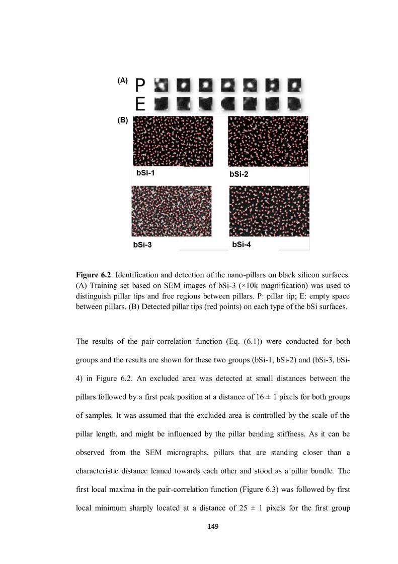
149
Figure 6.2. Identification and detection of the nano-pillars on black silicon surfaces.
(A) Training set based on SEM images of bSi-3 (×10k magnification) was used to
distinguish pillar tips and free regions between pillars. P: pillar tip; E: empty space
between pillars. (B) Detected pillar tips (red points) on each type of the bSi surfaces.
The results of the pair-correlation function (Eq. (6.1)) were conducted for both
groups and the results are shown for these two groups (bSi-1, bSi-2) and (bSi-3, bSi-
4) in Figure 6.2. An excluded area was detected at small distances between the
pillars followed by a first peak position at a distance of 16 ± 1 pixels for both groups
of samples. It was assumed that the excluded area is controlled by the scale of the
pillar length, and might be influenced by the pillar bending stiffness. As it can be
observed from the SEM micrographs, pillars that are standing closer than a
characteristic distance leaned towards each other and stood as a pillar bundle. The
first local maxima in the pair-correlation function (Figure 6.3) was followed by first
local minimum sharply located at a distance of 25 ± 1 pixels for the first group

150
(Figure 6.3 (A)). In comparison, the second group (Figure 6.3 (B)) showed first local
minima, which were weakly pronounced within an interval of 22 ± 3 pixels
confirming the differential nano-architechture between the two groups of bSi
surfaces.
Figure 6.3. Pair correlation function (Eq. (6.1)) of pillar tip positions as a function of
distance between pair of pillars for bSi-1 and bSi-2 (A) and bSi-3 and bSi-4 (B). The
up- and down arrows indicate approximate positions of the first peak and minima,
respectively.

151
6.3.2. Surface chemistry
The surface elemental composition of the black silicon samples was studied using X-
ray photoelectron spectroscopy (XPS). High resolution scans were performed across
C 1s, O 1s, F 1s and Si 2s peaks and the atomic percentages among all the surfaces
were similar. However, the total metallic Si elemental ratio as (Si/SiO2) in the
surface was varied between 1.2 and 2.2 (Table 6.1). The total Si content was found
to be in the range of 27-35% for all the black silicon samples. Previous studies have
reported that bSi surface is primarily amorphous Si with a small degree of surface
oxidation arising from the processing stage (Ivanova et al., 2013a). It can be
observed from the table below that the surface chemistry remains much the same for
all the samples under examination and it does not play a major role in determining
the fate of the bSi surfaces as a bactericidal surface.
Table 6.1. XPS analysis of bSi surfaces.
6.4. Nano-architecture dependent wettability
The next section will highlight the effect of surface topology and the surface chemistry on
the wettability of an individual surface. The study shown below will help to illustrate the
fact that the physical parameters of the nano-structures formed on a surface strongly affect
the wettability of the surface.
Element (%) bSi-1 bSi-2 bSi-3 bSi-4 Si 26% 27% 29% 35%
SiO2 21% 20% 18% 16% Si/SiO2 ratio 1.2 1.3 1.6 2.2

152
6.4.1. Surface topology affects wettability
The morphology variation of the nano pillars of the black silicon surfaces resulted in
changes in their wettability and average surface roughness (see pillar geometrical
parameters and surface roughness analysis in Table 6.2). The pillars on bSi-1 and bSi-2
were regularly and closely spaced with minimum inter-pillar spacing gap, whereas the
nano pillars on the bSi-4 were significantly longer with an average height of 1063 nm and
wider at their tips with an average width of 120 nm. Contact angle measurements indicated
that while bSi-1 and bSi-2 were found to be significantly hydrophobic with a WCA of 130º
and 100º respectively, bSi-3 was hydrophilic and bSi-4 was super hydrophilic which
resulted in complete wetting of the surface. BSi-4 surface produced a higher diameter of
~100 nm and fewer numbers of pillars and these pillars had less tendency to aggregate at
the tips and were well separated. It should also be noted that bSi-4 nano-pillars were
unusually thin and are sharply tapered towards the head of the pillars. The variation of
tapering at the waist of the pillars and proximity of the pillars from each other affected the
pillars’ propensity to aggregate at the tips, as this was mainly dependent on the pillars
flexural strength. The nano-pillars also seemed to vary in the configuration from being
conical to sharply taper at the tip heads.

153
Figure 6.4. Typical two-dimensional AFM images (2.5 µm × 2.5 µm scanning areas)
and corresponding cross-sectional profiles of black silicon surfaces. Scale bar is 2
µm.
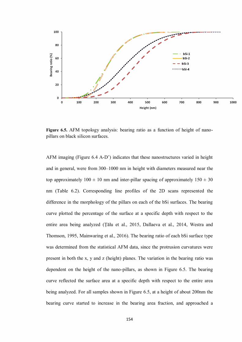
154
Figure 6.5. AFM topology analysis: bearing ratio as a function of height of nano-pillars on black silicon surfaces.
AFM imaging (Figure 6.4 A-D’) indicates that these nanostructures varied in height
and in general, were from 300–1000 nm in height with diameters measured near the
top approximately 100 ± 10 nm and inter-pillar spacing of approximately 150 ± 30
nm (Table 6.2). Corresponding line profiles of the 2D scans represented the
difference in the morphology of the pillars on each of the bSi surfaces. The bearing
curve plotted the percentage of the surface at a specific depth with respect to the
entire area being analyzed (Ţălu et al., 2015, Dallaeva et al., 2014, Westra and
Thomson, 1995, Mainwaring et al., 2016). The bearing ratio of each bSi surface type
was determined from the statistical AFM data, since the protrusion curvatures were
present in both the x, y and z (height) planes. The variation in the bearing ratio was
dependent on the height of the nano-pillars, as shown in Figure 6.5. The bearing
curve reflected the surface area at a specific depth with respect to the entire area
being analyzed. For all samples shown in Figure 6.5, at a height of about 200nm the
bearing curve started to increase in the bearing area fraction, and approached a

155
constant bearing area level within several 100nm. The increase indicated the volume
of everything present above the surface, which was the volume of the pillars. It
appeared that bSi-1 and bSi-2 samples reached a constant bearing area level at
approximately 500 nm, while the bSi-3 and bSi-4 samples reached a constant bearing
area level at approximately 800 nm, highlighting the nano-pillar height present on
each surface. Thus, from the AFM statistical analysis of the bearing ratio, it could be
inferred that the bSi-1 and bSi-2 and the bSi-3 and bSi-4 substrates could be grouped
together according to the data presented on the bearing curve.
6.4.2. Surface chemistry affects wettability
A correlation between the black silicon surface oxidation (Si/SiO2) and the wettability
can be observed (Table 6.2). The observed WCA trend with Si/SiO2 reveals that WCA
decreases with increasing elemental Si ratio. XPS data has been used to compare the
percentage atomic fractions of metallic Si, SiO2 and the Si/SiO2 ratios with the respective
contact angles of the black silicon surfaces. Total Si content was found to be increasing
with decreasing wettability. BSi-1 and BSi-2 with a contact angle of 130 and 100 had
~27% Si on their top surfaces; whereas the highest amount of Si (~35%) was found on
BSi-4, which was super hydrophilic with a contact angle of 0. Much to the contrary, the
relationship with % fraction of SiO2 with the wettability values observed a completely
opposite trend as compared to the former. 16% SiO2 was formed on BSi-4 (super
hydrophilic) sample whereas ~20-22% of SiO2 was found on the top surfaces of BSi-1 and
BSi-2 (hydrophobic) surfaces respectively. This can be attributed to the fact that RIE is
basically a surface phenomenon where silicon wafers have been subjected to SFx and Ox
ions respectively (Schwartz and Schaible, 1979, Marty et al., 2005, Jansen et al., 1995).
Oxygen ions help to passivate the silicon base substrate effectively oxidizing the surface

156
which results in the formation of SiO2 on the top layers. A high amount of Silicon and a
very low amount of SiO2 are indicative of the fact that the base substrate is not oxidized
upto completion and this in turn has affected the wettability of the sample in question. It
has been reported previously that black silicon surfaces are comparatively less
hydrophobic than their natural counterparts such as dragonfly wings largely due to the
phenomenon of surface oxidation, occurring during the fabrication process (Ivanova et al.,
2013a).
Table 6.2. Statistical analysis of geometrical aspects and surface roughness analysisa
of nano pillars and bSi surfaces
a AFM roughness analysis, 2.5 µm × 2.5 µm scanning area
b SEM micrographs
The visible reduction in the contact angle of the bSi surfaces, i.e from being super
hydrophobic to super hydrophilic of the black silicon samples can be explained with
Parameters bSi-1 bSi-2 bSi-3 bSi-4
Wettability
Water contact angle θ
(deg)
~130.8 ± 0.5 ~100.9 ± 0.6 ~40.1 ± 0.3 ~0.0 ± 0.0
Surface roughnessa
Average roughness
(nm) Ra
82.3 ± 0.2 110.3 ± 31.6 81.3 ± 57.4 124.7 ± 3.7
Root mean square
roughness (nm) Rq
103.7 ± 1.6 136.5 ± 37.4 144.9 ± 5.4 156.8 ± 4.9
Geometrical parametersb
Height (nm) 836.8 ± 1.2 657.9 ± 2.3 652.7 ± 1.3 1063.2 ± 1.1
Tip width 100.1 ± 0.5 110.3 ± 1.0 100.7 ± 0.8 120.5 ± 1.0
Inter pillar distance
(nm)
153.11 ± 55.29 135.58 ± 33.86 114.69 ± 33.22 197.41 ± 13.96
Density/µm2 10.7 10.6 12.2 8.2
Aspect ratio 8.4 6.0 6.5 8.8
Chemical composition
Si/SiO2 1.2 1.3 1.6 2.2
Si (At. %) 26 27 29 35
157
relation to the surface roughness and Cassie-Baxter and Wenzel models of surface
wettability. According to the Cassie model, air remains trapped below the drop and the
surface, thus forming air pockets (Giacomello et al., 2012, Choi et al., 2009b).
Hydrophobicity of the surface is enhanced as the solvent drop sits partially on air and fails
to make complete contact with the nano-structured surface. According to the Wenzel
model, surface roughness increases the surface area, which also significantly modifies
hydrophobicity (Bormashenko et al., 2007, Whyman et al., 2008, Murakami et al., 2014).
The average roughness of bSi-1 was found to be ~ 82.3 nm while the roughness of bSi-4
was ~124 nm. This change in surface roughness results in the apparent drop of the wetting
ability of the surface from that of being super hydrophobic to super hydrophilic. It has also
been reported that physical conditions of these nano-pillared surfaces that can strongly
affect the wetting transition include the height of nano pillars, the spacing between pillars
and the intrinsic contact angle(Koishi et al., 2009, Peters et al., 2009). There exists a
critical pillar spacing beyond which water droplets on the pillared surface can be either in
the Wenzel state or in the Cassie state, depending on their initial location. These studies
also well-match with our observations since bSi with the highest pillar density was found
to be super hydrophobic while bSi-4 with the least pillar density was almost super
hydrophilic where the drop completely spread on the surface.
6.5. Nano-structure dependent variable bactericidal activity
The morphological appearances of P. aeruginosa ATCC 9027 and gram-positive S. aureus
65.8T that adhered to bSi surfaces were significantly different from those that were
attached on the plain silicon surfaces (Figure 6.6 and Figure 6.7). The cell damage was
visible upon interaction of the cells with the nano-pillars. Viability analysis confirmed that
the surfaces displayed bactericidal activity towards the two studied bacterial strains. It was
observed that bSi surfaces were more effective in rupturing P. aeruginosa whereas, the

158
rate of selective killing of S. aureus was comparatively weaker. Our previous published
reports have pointed out that the successful elimination of bacterial cells mainly occurs due
to the forces incurred on the bacterial cell membranes upon interacting with the
nanostructured surfaces such as cell deformation, engulfment and subsequent pillar
penetration rendering the cells damaged (Hasan et al., 2013b, Pogodin et al., 2013, Ivanova
et al., 2013a). These forces have been more predominant on Gram negative Pseudomonas
aeruginosa due to the absence of a rigid external cell wall membrane, as seen in Gram
positive Staphylococcus aureus. However, it was observed that all the 4 black silicon
surfaces responded differently towards individual bactericidal activities. As a result, the
bacterial cells interacted with more “point-of-contacts” upon first landing with minimum
spacing between the heads. This interaction with the surface helped to puncture the cells
and the cluster of pillars were able to pierce the cells, leaving them damaged. The rest of
the surfaces, on the other hand provided less points of interaction with the bacterial cells
with adequate spacing for the cells to settle at the bottom. This settlement of the bacterial
cells is relatively harder to be eliminated and prolonged settlement of cultures leads to a
biofilm formation on the surface. In light of an antibacterial nano-structured surface, it is
important that the nano-structures are dense and effective from the very first interaction
with the bacterial cells.
Furthermore, a cell viability analysis was performed on all samples, and it revealed
substantially different levels of bactericidal efficiency for the four bSi types, with the bSi-3
and bSi-4 samples displaying the lowest level of bactericidal activity. For example, the
bactericidal efficiency of the bSi-4 surface towards S. aureus cells was determined to be
0.5 × 10⁵ cells min/cm2, whereas the bactericidal efficiency of the bSi-2 surface towards
the same bacteria was found to be considerably higher (4.2 × 10⁵ cells min/cm2), the
highest S. aureus killing rate of all the bSi samples being investigated (Figure 6.6).

159
While four types of studied bSi surfaces were found to be rather similar and possessed
several characteristics such as aspect ratio (6.0 - 8.8), pillar interspacing (150 ± 30 nm) and
density (8 – 12), which could not directly be correlated with the extend of the bactericidal
activity, AFM bearing statistics and neuronal networking analysis (Figures 6.4-6.6)
allowed to distinguish two groups of the nanostructured surfaces in relation to their
bactericidal performance. A summary of the neuronal networking analysis of the pillars
distribution for bSi-1 and bSi-2 and bSi-3 and bSi-4 surfaces, as inferred from the found
positions of first local maxima and minima in the pair-correlation function is shown in
Figure 6.6 (C), where a direct comparison with experimental data of the bactericidal effect
is provided (Figure 6 (A), (B)). In the second group (bSi-3 and bSi-4) the first minimum
was found at a slightly smaller distance, R, as compared to the first group (bSi-1, bSi-2),
while there was a larger uncertainty with respect to the position as indicated by the larger
error bar. When comparing the two groups with respect to bactericidal efficiency, these
detected although small differences in characteristics beyond the first peak of the pair-
correlation function reflected in a lower bactericidal efficiency of the second group as
compared to the first group. However, the exact relationship between the pillar position
relationships and bactericidal effect needs a more rigorous investigation.

160
Figure 6.6. Bactericidal efficiency of black silicon surfaces. (A) SEM images of P.
aeruginosa, S. aureus cells, which appeared to be disrupted through interaction with bSi
surfaces. Scale bar is 200 nm. CLSM images showing the proportion of live and dead
cells, live cells stained with SYTO® 9 (green) and non-viable cells stained with Propidium
Iodide (red). Scale bar is 5 µm. (B) Bactericidal efficiencies of bSi surfaces were evaluated
over a period of 3 h by using a standard plate count method. (C) Maxima and minima
positions of the pillar tip pair-correlation functions of bSi-1 to 4 as illustrated in Figure
6.3.

161
Figure 6.7. Cell morphology on control surfaces. Representative SEM images represent intact and healthy bacterial morphology of (A) P. aeruginosa and (B) S. aureus on control Si surfaces. Scale bar is 200nm.
Surface topography has been observed as a major player in predicting the interaction
between the bacterial cell and the nano-architecture of the surface. Available surface
area largely depends upon the active area the bacterial cells have in order to settle down
in the first few hours of incubation. A large area/pillar value would indicate that the
available pillar heads are fewer in number but have a large available area. On the
contrary, a small area/pillar value represents the presence of a large number of pillars
but with minimal contact area on their tips (Friedlander et al., 2013). This signifies that
recessed areas between the nano-pillars become less accessible to the bacterial cells if
the pillars have a high density and are closely packed. Previous studies report that nano-
structured surfaces with sub micrometer sized recession areas are able to accommodate
cells between the nano protrusions, which makes elimination of these cells rather
difficult to achieve (Chung et al., 2007, Xu and Siedlecki, 2012). One of our previous
studies has also explained a biophysical model that reflects upon the rupture of the cells
when they come in contact with the nano structured surfaces (Pogodin et al., 2013).
Cells have been observed to try to maximize their contact area with the surface in order
to achieve a strong and stable attachment (Hsu et al., 2013). Therefore, to achieve a

162
significant bactericidal activity, it is highly desirable that the available pillar height and
the density be maximized so that more pillar heads can interact with the cell causing
irreversible damage to the cell membranes.
6.6. Summary
The results of this work provide evidence that despite a range of bSi substrates having a
nano-architecture with visual similarity, the bactericidal efficiency of such substrates can
vary considerably. In this study, we have evaluated several of the nanometer-scale
characteristics of bSi surfaces that may influence their bactericidal efficiency; these
characteristics included the surface chemistry and wettability, the nano-pillar height and
density, surface topography, aspect ratio of the surface nano-features, AFM topology
based on the bearing ratio as a function of the height of the nano-pillars, and a neural
network analysis to characterize the pillar tips and their distribution. Less bactericidal bSi
surfaces were found being hydrophilic, contain nano-pillars of heights reaching 1000 nm
that were not always well-separated, with aspect ratios between 6 and 8.8, reaching the
constant level of surface area at 800 nm with respect to the entire area being analyzed, and
with low local maxima and minima positions of the pillar tip pair-correlation function. In
summary, we have demonstrated that among the black silicon surfaces that possessed a
similar surface nano-pattern, the bactericidal efficiency brought about by the nano-
topology of the pillars on each of the surfaces varied considerably. Although all the bSi
surfaces were capable of killing P. aeruginosa, and S. aureus bacterial cells, the killing
rate, expressed as 104 cells killed cm-2 min-1, could vary by up to an order of magnitude.
We therefore hypothesize that the nano-topology of the surface, as seen by the precision of
the pillar nano-architecture functionality, is related to the bactericidal efficiency of an
individual surface.

163
Chapter 7
Construction of a bactericidal microfluidic
device using nano-textured black silicon
164
7.1. Overview
Antibacterial surfaces (Zhuang et al., 2012, Ivanova et al., 2012a, Broderick et al.,
2013) are becoming imperative in applications designed to curb the negative
consequences associated with resistance to antibiotics present in food, water, and soil
(Jain et al., 2014, Arias and Murray, 2009, Levy, 1998). Bacterial resistance arising
from their exposure to antibiotics has the potential to compromise our immune
system, particularly with regard to our ability to effectively resist bacterial infections
(Andersson, 2003, Singh et al., 2002). Many natural and synthetic surfaces achieve
their self-cleaning, anti-fouling and/or bactericidal properties through various
mechanisms; they can be highly oxidative, becoming bactericidal when activated by
UV-light (Sakai et al., 2012) self-cleaning due to their surfaces being rendered
hydrophobic via modification of their chemical or mechanical properties (Santra and
Tseng, 2013, Kikuchi et al., 1997, Kairyte et al., 2013), or anti-fouling due to their
surface structures sterically hindering the attachment of pathogens (Jain et al., 2014,
Graham and Cady, 2014). Other applications of micro- and nano-structured surfaces
in the biomedical industry include dermal patches, which possess painless needles
that allow the controlled release of drugs, and bandages that possess bio-compatible
microfibers that trigger increased levels of healing when exposed to ultraviolet UV
light (Guimarães et al., 2015). Surfaces that display mechanical means for
antifouling and antibacterial properties are a topic of significant research as they
provide a substrate from which a fundamental understanding of the mechanism takes
place (Hasan et al., 2013a, Webb et al., 2015, Bixler and Bhushan, 2015, Graham et
al., 2013). These surfaces also have wide applications in the production of sanitary
surfaces such as mobile telephones and other household items (Park et al., 2012b,
Machida et al., 2005).

165
The search for inexpensive methods for the fabrication of large area nano-textured
surfaces is currently underway. Silicon is a substratum that has been used
extensively in the semiconductor and solar cell industries (Mavrokefalos et al., 2012,
Liu et al., 2012, Hauser et al., 2012, Reece et al., 2011, Huang et al., 2012). Being a
relatively inexpensive product, silicon represents one of the best substrata for the
fabrication of large areas of nano-textured surfaces, where reproducible surfaces are
currently able to be prepared over surfaces of several centimetres in diameter. Such
substrata can also have electrical and photo-electrochemical device level
functionalities incorporated into their surface, which is useful when producing
micro-chips (Savin et al., 2015). Methods for preparing these nano-textured surfaces
using a silicon substratum include plasma etching, where the deposition of electrical
contacts is required for the fabrication of wafer sized bSi surfaces (Sainiemi et al.,
2011, Otto et al., 2012, Gaudig et al., 2015, Nguyen et al., 2012, Nguyen et al.,
2013a). The unique nano-topography of bSi forms due to the self-organized hard
mask that results from the first few seconds of etching (Jansen et al., 1995, Jansen et
al., 2009). These are specific to the chemistry and chamber materials being used for
the production of the bSi (Jansen et al., 2009). It is used in high efficiency solar cells,
as it represents a low reflectance or broadband absorbing surface. More recently it
has been used for the production of sensors that are based on surface enhanced
Raman scattering (SERS) (Seniutinas et al., 2015). bSi substrata have recently been
produced that possess a similar surface topography to that of dragonfly wings, and
have been found to exhibit a similar bactericidal efficiency when coming in contact
with pathogenic bacteria and spores (Ivanova et al., 2013a).
166
Given this demonstrated bactericidal functionality of the bSi surface, a microfluidic
device has been constructed incorporating a bSi substrate to investigate whether this
bactericidal action would be effectively translated within a flow channel of a
microfluidic device against Pseudomonas aeruginosa. A narrow 15 µm high and 1
cm wide flat flow channel was constructed that allowed the bacteria to come into
contact with the bactericidal nano-spikes present on the surface of the bSi. The large
1 × 2 cm2 surface area of the bSi was shown to be efficient in being able to kill an
infectious dose of Pseudomonas aeruginosa, achieving an approximate 99% killing
efficiency. The flow rate required to fill the bSi chamber was found to be 0.1 µL/s,
with a 10 min equilibration time being allowed for the bacterial cells to interact with
the bSi surface. Complete rupturing of E. coli cells was also achieved after 15 cycles,
allowing the effective release of cellular proteins from within the bacterial cells (65.2
µg/mL from 3 × 10⁸ cells/mL). The channel was then able to be re-used after
washing with 10 successive cycles of sterile MilliQ water and PBS. Larger volumes
of bacterial suspensions have the potential to be treated using a similar flow channel
configuration if the dimensions of the flow channel are scaled accordingly. This
bactericidal microfluidic device provides a novel platform for studies carried out
under both static and dynamic (flow) conditions.
7.2. Design and conceptualization of a 3-dimensional bSi
microfluidic device
A general schematic of the step-by-step construction of the microfluidic device has
been presented in Figure 7.1. The bSi was prepared using a plasma etching process
(Seniutinas et al., 2015, Gervinskas et al., 2011). An Oxford PlasmaLab 100 ICP380
plasma etcher was used for patterning the surface of p-type boron-doped 4-inch
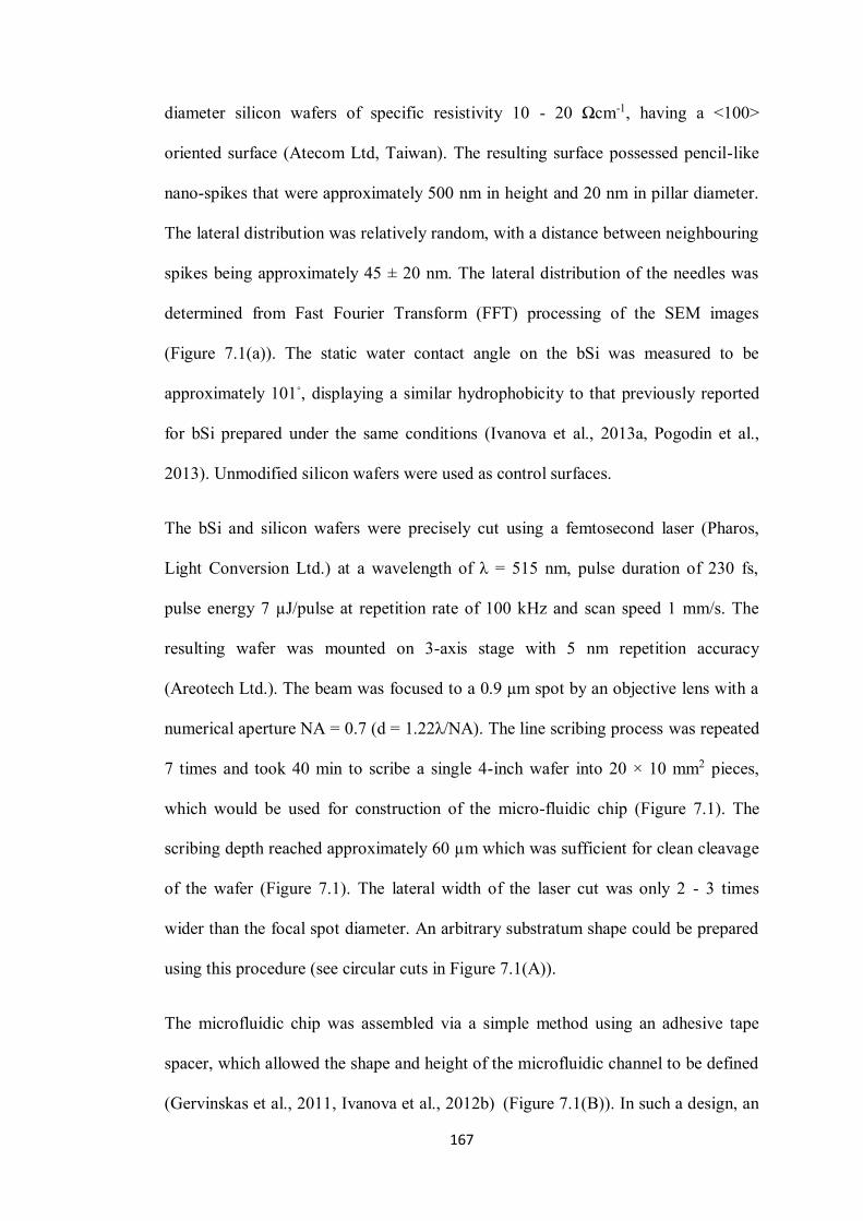
167
diameter silicon wafers of specific resistivity 10 - 20 Ωcm-1, having a <100>
oriented surface (Atecom Ltd, Taiwan). The resulting surface possessed pencil-like
nano-spikes that were approximately 500 nm in height and 20 nm in pillar diameter.
The lateral distribution was relatively random, with a distance between neighbouring
spikes being approximately 45 ± 20 nm. The lateral distribution of the needles was
determined from Fast Fourier Transform (FFT) processing of the SEM images
(Figure 7.1(a)). The static water contact angle on the bSi was measured to be
approximately 101, displaying a similar hydrophobicity to that previously reported
for bSi prepared under the same conditions (Ivanova et al., 2013a, Pogodin et al.,
2013). Unmodified silicon wafers were used as control surfaces.
The bSi and silicon wafers were precisely cut using a femtosecond laser (Pharos,
Light Conversion Ltd.) at a wavelength of λ = 515 nm, pulse duration of 230 fs,
pulse energy 7 µJ/pulse at repetition rate of 100 kHz and scan speed 1 mm/s. The
resulting wafer was mounted on 3-axis stage with 5 nm repetition accuracy
(Areotech Ltd.). The beam was focused to a 0.9 µm spot by an objective lens with a
numerical aperture NA = 0.7 (d = 1.22λ/NA). The line scribing process was repeated
7 times and took 40 min to scribe a single 4-inch wafer into 20 × 10 mm2 pieces,
which would be used for construction of the micro-fluidic chip (Figure 7.1). The
scribing depth reached approximately 60 µm which was sufficient for clean cleavage
of the wafer (Figure 7.1). The lateral width of the laser cut was only 2 - 3 times
wider than the focal spot diameter. An arbitrary substratum shape could be prepared
using this procedure (see circular cuts in Figure 7.1(A)).
The microfluidic chip was assembled via a simple method using an adhesive tape
spacer, which allowed the shape and height of the microfluidic channel to be defined
(Gervinskas et al., 2011, Ivanova et al., 2012b) (Figure 7.1(B)). In such a design, an

168
adhesive double sided tape (ARclad IS-8026-15, Adhesives Research Inc.) was
placed on the glass substratum with the channel layout being defined by a laser cutter
(CO2 laser VLS 2.30, Versa Laser). The chip was completed by placing the top plate
of the bSi in position and sealing the device with silicone. The tubing, obtained from
syringe needles, was added and sealed in position, as required. Duplicate chips,
fabricated using the control silicon wafer substrates, were used as negative controls.
The channel height of both the bSi and control chips was 15 µm, determined by the
thickness of the adhesive tape used in the construction of the device. This height was
selected in order to accommodate the rod-shaped P. aeruginosa cells, which had
dimensions of approximately 2 µm × 1 µm (Vallet-Gely and Boccard, 2013).

169
Figure 7.1. (A) High resolution SEM image (top view) of bSi with a Fast Fourier Transform (FFT) inset. Side and top view SEM images (bottom) of laser scribed line used for cleaving 400-µm-thick Si wafer. (B) Micrograph of the assembled chip (top) and assembly schematic (1 to 5) with adhesive film defining the channel height, t ~15 µm.
The flow cell dimensions were optimised to achieve efficient elimination of bacterial
cells by restricting the instances of several bacterial cells being present within the
cells on top of each other, maximising their exposure to the nano-textured surface of
the black silicon. The fabricated microfluidic device contained a 2 × 1 cm2 section of
bSi, with a 15 µm gap above the bSi surface, which is almost a twofold reduction in
available volume compared with previous cell designs (Gervinskas et al., 2012). This
reduction in volume was essential in order to ensure an efficient interaction occurred
between the bSi surface and the bacterial suspension during flow. The wall effect
causes a larger viscous drag near the substrate (Miwa et al., 2000) with a faster flow

170
being present in the centre of the cell. This means that there was a greater probability
that bacteria could be located at the centre, or mid-height, of the channel. When the
flow was paused for the bacteria to come into contact with the bSi surface, the larger
width and large surface area of bSi were also key features of the microfluidic chip.
The peristaltic pump was pushing the P. aeruginosa cells through the channel, and a
uniform advancing front of air-liquid interface was observed under the microscope,
confirming the uniform height of the channel over the entire area of the bSi.
7.3. Bactericidal activity of the bSi embedded microfluidic device
To quantify the bactericidal performance of the flow channel, a portion of bacterial
solution that had passed through the microfluidic device was sampled after each
cycle and plated onto agar plates (Figure 7.2). The efficient bactericidal action of the
bSi surface was confirmed using standard staining techniques using Propidium
Iodide (red) for non-viable and SYTO 9 (green) for viable bacterial cells,
respectively (Figure 7.3).

171
Figure 7.2. Schematic of filtering a bacterial suspension through the bSi microfluidic chip followed by subsequent viability tests (A-D). Optical images showing the viability of P. aeruginosa cells before and after introducing the cells into the flow channel.
The SEM images of the bacterial cells on the bSi surface revealed changed cell
morphology confirming that structural damage to the cells had occurred. There was,
however, no evidence of damaged bacterial cells present on the microfluidic channel
with the control silicon surface, as confirmed by confocal and SEM image analysis
(Figure 7.3).

172
Figure 7.3. Bactericidal effect of the microfluidic device. (A) CLSM image of fluorescently labelled P. aeruginosa cells and (B) SEM image of P. aeruginosa cells on control silicon surface. Confocal image (C) and SEM (D) images of P. aeruginosa cells on bSi surface. Confocal images have been taken after 10 min of cells being in contact with substratum: Si or bSi. Bacterial cells are stained with SYTO 9 (green) and Propidium Iodide (red) indicating live and dead bacteria, respectively.
The results presented in Figure 7.4 (A) demonstrated that the elimination of bacterial
cells from the initial suspension was dependent on the number of filtering cycles to
which the initial suspension was subjected. It is shown that an approximate reduction
of ~99% P. aeruginosa cells was achieved within 5 cycles of the bacterial

173
suspension through the channel. A slight reduction in the concentration of bacterial
cells was also observed for the control, which is expected. The bactericidal
efficiency of the bSi-containing microfluidic device was calculated by subtracting
the extent of bacterial removal using the control microfluidic device under the same
experimental conditions, the results of which are presented in Figure 7.4 (B). The
bacterial killing rate was calculated as a log10 reduction value to analyse the
bactericidal rate on a comparative scale, which revealed that up to 99% of the cells
were killed after 5 consecutive cycles through the bSi-containing microfluidic
device. It has to be taken into consideration that each cycle conforms to 45 s of
filling the chamber followed by a 10 min stoppage time.

174
Figure 7.4. Bactericidal performance of the microfluidic bSi channel. (A) Log10 reduction of P. aeruginosa cells has been calculated for each set of experiments for 5 cycle runs. (B) The killing rate of bacteria versus number of cycles through the bSi channel.
The 10-minute flow stoppage that occurred during the bacterial flow through the
microfluidic device was undertaken to allow the bacterial cells sufficient time to
come into contact with the bSi surface within the cell. The average thermal velocity
that occurs through this process was estimated by assuming equality between the
kinetic and thermal energies taking place. This was calculated using
v= √ (3kbT/m) ≈ 1.0 mm/s (7.1)
where kb is the Boltzmann constant, T = 293 K is the absolute temperature at normal
conditions, and m ~10.0 pg is the mass of a single P. aeruginosa cell. The mean

175
displacement of bacteria over time (t) occurs due to Brownian motion, and is
calculated according to
∆x (t) = √ (32mtv2 /81πμr) (7.2)
where µ = 8.9 × 10⁻⁴ Pa s is the dynamic viscosity of water. It takes only t ~ 2 min
for bacteria to move over ∆x (t) = 15 µm which is comparable with the height of the
microfluidic channel. During the total exposure period, it is therefore almost certain
that the bacteria would have come into contact with the bSi surface within the
microfluidic device.
7.4. Application of bSi microfluidic device towards proteomics
It is crucial to integrate cell lysis and fractionation steps to achieve a total micro
analytical system for the analysis of cells and their constituent proteins on-chip,
without adding extra steps (Aran et al., 2011). To determine the same functionality,
the microfluidic channel was used to quantify the release of the total cellular proteins
from ruptured E. coli cells from the cell suspension, which was being circulated
through the channel (Figure 7.5). The protein concentration was monitored after each
cycle and over the entire 15 cycles. An additional 5 cycles were performed to ensure
the complete extraction of proteins. Approximately 65.2 µg/mL of cellular protein
was extracted after 15 cycles, as confirmed using Bradford’s assay (Table 7.1).

176
Table 7.1. Comparative protein extraction from E. coli cells
*From 3 × 10⁸ cells/mL
These results are in agreement with an estimated amount of 60 - 66 µg/mL of total
cellular proteins, which can be obtained from 3 × 10⁸ cells/mL, taking into account
that a single E. coli cell contains ~0.2 pg protein (Dattolo et al., 2010). Notably, it
appeared that the combined enzyme and sonication treatment was less efficient in
extracting the cellular proteins than the mechanical rupture method that occurred
within the microfluidic device, which resulted in total cellular protein yield of 52.7
µg/mL.
Cell lysis technique (s) Protein concentration* (µg/mL) Theoretical estimation ~ 60-66
Microfluidic channel 65.2
Sonication 29.6
Enzyme treatment and sonication 52.7

177
Figure 7.5. Estimation of total proteins released from E. coli cells. A linear gradient has been drawn to signify the increasing amount of extracted proteins. Protein extraction from initial E. coli cells suspension and the Si channel has been included as controls.
To assess whether the bSi-containing microfluidic device was able to be cleaned and
re-used, a single flush of the device using PBS buffer solution was carried out at a
5.7 µL/s flow rate for 4 s followed by 10 successive cycles of Milli-Q water. Each
flush was carried out at a rate of 5.7 µL/s for a period of 4 s, followed by a forward
and backward flow for 2 s each. After the washing cycle, there was no evidence of
any viable bacteria being present within the device, as confirmed by the direct
colony counting technique. The total time required for cleaning the microfluidic
device was 1 minute.

178
7.5. Summary
In this study, a simple method was used to fabricate a microfluidic device containing
a channel that was 15 µm in height over a relatively large 2 cm2 area. Incorporation
of bSi into the device design resulted in a device that was bactericidal when flow
into the cell was paused for 10 min after filling the cell, which took 45s.
Approximately 99% of P. aeruginosa cells from the infectious dose were eliminated
after 5 successive fill-stop cycles through the device. The newly designed
microfluidic device was also used for the effective extraction of cellular protein from
the ruptured E. coli bacterial cells. The device was shown to be re-used after multiple
steps of washing using a simple high speed flushing process.
In a previous study (Gervinskas et al., 2012), where a very high flow speed of more
than 1 m/s were used when pumping polystyrene bead suspensions through a
microfluidic device with channels containing sharp micron-sized features, the beads
were seen to be able to avoid contact with the sharp features by following the
laminar flow within the channel. Since the bSi components of the microfluidic
devices used in the current study were prepared from 4-inch wafers, it is possible to
construct a microfluidic device that contains wider and longer bSi sections, and
perhaps to also contain multiple bSi channels for sequentially treating bacterial
solutions. Studies involving such components would reveal whether it is possible to
design a device for testing the bacterial contamination of grey water. The
bactericidal action of the bSi component of the microfluidic devices could be further
improved by incorporating ultraviolet light-emitting diodes, making such devices
applicable to a wide range of water disinfection and sterilisation applications (Nelson
et al., 2013, Shatalov et al., 2012, Venancio-Marques et al., 2013, Würtele et al.,

179
2011, Mori et al., 2007). The microfluidic device reported here has demonstrated that
it has a high sensitivity for the refractive index of the solution being used;
∆λ/∆n = 390 nm/RIU (refractive index units) (Huang et al., 2012) (7.3)
and could be further assessed for its ability to recognise bacterial (or other)
contamination by incorporating a section within the device that contains Fabry-Pérot
mirrors on the upper and lower walls of the channel. Such a microfluidic device
would allow the in situ monitoring of refractive index changes that could be related
to the removal of bacteria from solution. An additive pressure (∆P), scales linearly
with the flow velocity (v) in the microfluidic device, for a liquid of viscosity (µ),
inside a channel with the transverse dimension height (t), width (w) and length (l)
according to:
∆P∝ µvl/(tw) (Tabeling, 2010). (7.4)
Hence for a longer and narrower channel, ∆P would increase with the second power
of the decreasing geometrical length and height dimensions. To maintain a high
throughput flow at as large as practical, the width of the channel should be increased.
Micro and nano-fabricated devices have been designed to expedite applied and basic
research into cell biology and morphology in dynamic flow through these devices
(Buividas et al., 2014, Wu and Dekker, 2016, Gao et al., 2012, Sackmann et al.,
2014). Protein analysis and quantification in clinical samples, such as blood serum or
whole-cell lysates presents certain challenges such as in the pre-treatment or
fractionation of complex samples for integration into the micro-analysis systems.
Several groups have developed microchip- or capillary-based two-dimensional
separation systems, which are an integration of micellar electrokinetic

180
chromatography (MEKC) or isoelectric focusing (IEF) with capillary electrophoresis
(Wang et al., 2004b, Rocklin et al., 2000, Mok et al., 2014, Lazar and Kabulski,
2013, Hu et al., 2011). These reports are, however limited by the fact that they are
quite complex systems, and a number of additional steps become involved in the
separation and identification of the desired protein analyte. A study has also been
published where E. coli cells have been lysed using a simple channel mechanism
(Schilling et al., 2002). This study, however, uses detergent addition as an additional
step to lyse the cells in flow, with the height and depth of the cell being 1000 µm and
100 µm, respectively. The width and height of this dimension could be detrimental to
the attachment pattern of bacteria, which are not more than 5 µm in their average
dimension. In an yet another finding, E. coli cells extracted from clinical samples
have been made to interact with specific antibodies for detection (Wang et al., 2012).
The device reported in our work avoids these extra steps, as the bactericidal bSi
surfaces have already been incorporated inside the channel to lyse the cells.
Moreover, the height of the channel is such that it prevents any specific instance of
the bacteria not coming into contact with the bSi.
The proposed simple microfluidic device with nanotextured bSi could be used for
surface enhanced Raman spectroscopy applications under the required flow
conditions. The device also has the capacity of incorporating electrodes to carry out
electrochemical surface cleaning (oxidation of adventitious carbon) and removal of
oxide (Buividas et al., 2014). Such flow devices that have the potential for
controlling the electrochemical potential and are expected to be useful for
investigations into detailed surface chemical reactions and catalysis, e.g., in the
generation of hydrogen (Juodkazytė et al., 2014, Juodkazis et al., 2010). The
evolution of oxygen through such electrodes could be achieved if an oxidative stress

181
can be applied to the bacterial cells. The incorporation of UV-LED treatment
sections into the device would also be possible.

182
Chapter 8
Construction and study of Gluconobacter oxydans
self-organized bio wires and their application as bio-
anodes in a microbial fuel cell (MFC)

183
8.1. Overview
Despite recent advances and technological innovations in microbial electrochemical
technologies, including the bio-production of biofuel, waste treatment and bio-
sensing (Babkina et al., 2006, Logan, 2009, ElMekawy et al., 2013, Huang et al.,
2011a), poor electron transfer between microbes and electrodes are a major concern
and limiting factor for large-scale applications of the technology (Logan, 2009,
ElMekawy et al., 2013, Huang et al., 2011a). In light of this drawback, intensive
research has concentrated on understanding the mechanisms responsible for the
extracellular electron transfer (EET) process and on the methods by which the
electrocatalytic bacteria co mmunicate (Marzocchi et al., 2014, Reguera et al., 2005,
Malvankar et al., 2011, Logan, 2009, Huang et al., 2011a, Pirbadian et al., 2014,
Gorby et al., 2006). It has been discovered that bacteria are able to form ‘pili-like’
nanowires that facilitate an EET process by linking the respiratory chains located on
the membranes of the bacterial cells to adjacent external surfaces, such as oxidized
metals in the natural environment or to engineered electrodes in renewable energy
devices (Huang et al., 2011a, Pirbadian et al., 2014, Gorby et al., 2006, Reguera et
al., 2005). Geobacter sulfurreducens bacterial cells have been reported to form the
pili that serve as the biological nanowires that allow the transfer of electrons from
the surface of the bacterial cells to the surface of Fe(III) oxides (Reguera et al., 2005,
Malvankar et al., 2011). In this work, metal-reducing Shewanella oneidensis MR-1
(Pirbadian et al., 2014, Gorby et al., 2006, Reguera et al., 2005) bacterial cells were
observed to form nanowires as extensions of their outer membrane and periplasm. It
was also reported that Shewanella oneidensis MR-1 cells that had been treated with
cisplatin produced elongated cells, which showed approximately a five-fold
improvement in current densities compared to normal, untreated cells (Patil et al.,

184
2013). Furthermore, filamentous bacteria of the family Desulfobulbaceae have been
found to conduct electricity over centimetre-long distances, thereby coupling the
processes of oxygen reduction at the surface of marine sediment with sulphite
oxidation in the sub-surface layers(Pfeffer et al., 2012, Marzocchi et al., 2014).
Gluconobacter oxydans cells require redox shuttles to assist the transfer of electrons
from the active sites on the cells to electrodes(Alferov et al., 2014, Babkina et al.,
2006, Deppenmeier et al., 2003, Reshetilov et al., 2006, Vostiar et al., 2004). This
Gram-negative, non-motile bacterium produces periplasmic membrane-bound
pyrroloquinoline quinone (PQQ), which contains complex enzymes that allow the
efficient oxidation of a number of substrates (Alferov et al., 2014, Babkina et al.,
2006, Deppenmeier et al., 2003, Prust et al., 2005, Reshetilov et al., 2006, Treu and
Minteer, 2008). G. oxydans is a promising candidate for the construction of efficient
microbial fuel cells due to the periplasmic localization of the active sites of the PQQ-
dependent redox enzymes(Alferov et al., 2014, Babkina et al., 2006, Deppenmeier et
al., 2003, Reshetilov et al., 2006, Treu and Minteer, 2008, Vostiar et al., 2004). In
particular, G. oxydans encapsulated in a confined space showed enhanced levels of
electric power generation (Alferov et al., 2014). It remains unclear, however, how
the G. oxydans cells were encapsulated within the polymeric hydrogels. This chapter
reports the mechanism by which G. oxydans subsp. industrius B-1280 cells are
encapsulated within the three dimensional confined environment of a hydrogel
system constructed from poly (vinyl alcohol) cross-linked with N-vinyl pyrrolidone.
The proposed mechanism is supported by experimental evidence in addition to
molecular dynamics simulations for the four exopolysaccharides (acetan, cellulose,
dextran, and levan) present on the outer cell wall of the G. oxydans cells
(Deppenmeier et al., 2003, De Muynck et al., 2007). Synthetic and analytical

185
chemistry techniques, including ultra-small-angle neutron scattering (USANS),
biological assays and computational modelling were used to demonstrate that G.
oxydans cells were actively engaged in self-encapsulation and were able to construct
a bio-wire network by utilizing the molecular components of the PVA-VP hydrogel.
Specifically, we showed that the interactions taking place between the bacterial
extracellular polysaccharide compounds and the surface loops of the PVA-PV
hydrogel had the greatest influence over the structure of the resultant hydrogel and
were able to completely transform its original three-dimensional structure into a
well-organized biowire network.
This chapter discusses a three-dimensional hydrogel system of poly (vinyl alcohol)
cross-linked with N-vinyl pyrrolidone (PVA-VP), developed in order to investigate
the mechanisms employed by the Gluconobacter oxydans subsp. industrius B-1280
bacteria for electron transfer (EET) in a three-dimensional hydrogel environment
Here we describe the formation of self-organized three-dimensional biowires that are
constructed by the G. oxydans, in which the cells are organized in a particular side-
by-side alignment. We demonstrated that the non-motile G. oxydans cells were able
to reorganize themselves, transforming and utilizing the PVA-VP polymeric
network. Molecular dynamics simulations of the G. oxydans EPS interacting with the
hydrogel polymeric network showed that the solvent-exposed loops of the PVA-VP
extended and engaged in bacteria self-encapsulation. This molecular reorganization
facilitated the formation of a functional biowire network, allowing the G. oxydans
cells to generate stable and efficient power.

186
8.2. Three-dimensional organisation of PVA-VP hydrogels
An in-depth understanding of hydrogel polymeric network structures and hydrogel-
associated water states is essential to allow the correlation of the physico-chemical
properties of three-dimensional structured systems containing a distribution of
bacterial cells (Pajic-Lijakovic et al., 2015, Tuson et al., 2012, Martinez et al., 2014).
Hydrogels of molecular weights 67 kDa and 125 kDa (henceforth abbreviated as L-
PVA and H-PVA) were synthesized in this study through the free radical
polymerization of linear poly (vinyl alcohol) (PVA) and a cross-linker N-vinyl
pyrrolidone (VP). Ceric ammonium nitrate (CAN) was used to initiate the chain
reaction, resulting in the formation of free radical species (shown in Figure 8.1(A)
(Athawale and Rathi, 1997, Pati and Nayak, 2012). Free oxygen radicals of PVA
were then cross-linked with the double bond present on the N-vinyl pyrrolidone
monomers, leading to the formation of a three-dimensional mesoporous polymeric
network, as confirmed by the SEM analysis of freeze-fractured hydrogel samples
(Figure 8.1 (B)). X-ray diffraction was used to understand the formation of the PVA
hydrogel mesoporous structures (Ricciardi et al., 2004, Holloway et al., 2013b, Kim
et al., 2015), indicating the presence of entangled, swollen amorphous and crystalline
domains of PVA acting as knots of the gel network (Figure 8.1). Raman micro-
spectroscopy imaging re-confirmed the formation of the PVA-VP mesoporous
structure of hydrogel films in their hydrated state (Figure 8.1(B)).

187
Figure 8.1. Synthetic pathway and physical characteristics of mesoporous poly (vinyl alcohol) (PVA) of molecular weights 67 kDa (L-PVA) and 125 kDa (H-PVA) crosslinked with N-vinyl pyrrolidone (VP). (A) Schematic illustration of the radical polymerization reaction between linear polymeric PVA and VP to form the hydrogel PVA-VP. (B) Mesoporous structures of hydrogel were visualised under freeze-fractured and hydrated states using scanning electron microscopy (scale bar is 5 μm) and Raman micro spectroscopy (scanning areas of 5 μm × 5 μm), allowing the visualization of the porosity dimensions of PVA-VP. (C) Pore diameter distribution of L-PVA-VP and H-PVA-VP estimated using Image J. (D) The difference in pore diameters between two hydrogels shown by ultra-small angle neutron scattering (USANS) spectra.
The estimated distribution of pore diameter is presented in (Figure 8.1 (C)). The
spectra of ultra-small angle neutron scattering (USANS) were used to highlight the
difference between structures of two hydrated hydrogels (Figure 1(D)) (Hule et al.,

188
2008, Iannuzzi et al., 2010). At the lower scattering length (q) of 10-3 to 10-4, the
scattering intensity of the L-PVA-VP was found to be higher than that of the H-
PVA-VP, which is consistent with the results obtained using SEM and Raman
spectroscopy (Figure 8.1(B) and (C)).
8.3. Characterization of PVA-VP hydrogels without and with G.
oxydans
8.3.1. G. oxydans biowire network formation and physico-
chemical characterization.
The G. oxydans cells in PVA-VP hydrogels were visualized using scanning electron
microscopy (SEM), confocal laser scanning microscopy (CLSM) and Raman micro-
spectroscopy (RM) (Figure 8.2 (A, B, C) and Figure 8.3). Examination of the freeze-
fractured hydrogels containing the bacterial cells showed that the original three-
dimensional organization of the both hydrogel types had been completely altered.
The G. oxydans cells were found to have self-organised into a bio wire network
(Figure 8.2 (A)). The results of this study indicated the presence of entangled
swollen amorphous and crystalline domains of PVA that acted as ‘knots’ within the
gel network. Raman micro-spectroscopic imaging of the samples also confirmed the
formation of a PVA-VP porous structure within the hydrogel films in their hydrated
state. Average bio wire cluster lengths were found to be 10.5 ± 6.4 μm and 12.6 ±
6.0 μm, respectively, for L-PVA-VP and H-PVA-VP, as inferred from Image J®
analysis (Figure 8.2 (D)). Examination of the CLSM micrographs revealed that the
G. oxydans cells secreted extracellular polymeric material and exhibited notable
side-by-side orientation within the formed bio wire (Figure 8.2 (B)).

189
Figure 8.2. Self-assembly of Gluconobacter oxydans sbsp. industrius B-1280 into bio wire clusters in PVA-VP hydrogel systems. (A) Scanning electron microscopy (SEM) showing the re-organization of G. oxydans into clusters wrapped with polymer. (B) Confocal laser scanning microscopy (viable cells stained with Syto9® (green) and non-viable cells stained with Propidium Iodide (red)) and (C) Raman micro-spectroscopy (scanning areas: 5 μm × 5 μm) showing G. oxydans clusters at hydrated states. (D) Cluster length distributions of G. oxydans showing that bacteria form the shorter length in a 67 kDa PVA-VP hydrogel in comparison to that of the 125 kDa PVA-VP hydrogel. Kinetics of G. oxydans self-organization in L-PVA-VP investigated using time lapsed (E) USANS and (F) CLSM. (G) Schematic illustration of the re-arrangement of bacteria, disrupting the polymeric network.

190
Figure 8.3. Comparative Raman spectra of G. oxydans (GO) encapsulated in low (L) and high (H) mol. weight PVA-VP hydrogels and unmodified L- and H-PVA-VP hydrogels. (A) Raman spectra (at 532 nm laser) of G. oxydans, hydrogel encapsulated G. oxydans and native hydrogel. (B) Raman imaging in 1600 to 1720 cm-1 Raman shift range with the intensity profile map of the same images of corresponding samples.

191
8.3.2. Swelling ratio analysis
The rate of water uptake of the PVA-VP hydrogels was evaluated by determining the
swelling ratio (Figure 8.4). For calculation purposes, the dry weight of the films was
recorded before the start of the experiment. An average value was obtained after 4
independent experiments. The equilibrium swelling ratio was then calculated using
Equation (8.1):
Swelling ratio (%) = [(Ws/Wd)/Wd] ×100 (8.1)
Where Ws denotes the weight of swollen film and Wd denotes the weight of dry film
(Hassan and Peppas, 2000b) (Hassan and Peppas, 2000a, Lee et al., 1996, Karimi et
al., 2013). The hydrogel samples were swollen in Milli-Q water for 30, 60, 90 and
120 minutes, respectively, at 25º C. The dry weights of the films were recorded at
the beginning of the experiment. The readings are taken at time duration of 120
minutes (2 hours) and the error bars represent measurements from 4 separate
individual readings. It was observed that that an equilibrium swelling value was
obtained after a time period of 120 minutes. After the stipulated time-period, the
hydrogels were wiped using a soft tissue paper to remove the excess water and the
analysed immediately.

192
Figure 8.4. Effect of G. oxydans encapsulation on the water retention potential of the mesoporous PVA-VP hydrogels. Swelling ratios of the PVA-VP hydrogels and their G. oxydans (GO) encapsulated counterparts.
The L-PVA-VP and H-PVA-VP hydrogels exhibited a pore diameter of 0.92 ± 0.38
and 1.08 ± 0.46 μm, respectively. The L-PVA-VP hydrogel exhibited a higher
swelling ratio of 410 % compared to that of the H-PVA-VP (220 %) hydrogel
(Figure 8.4), most likely due to the lower proportion of crystalline segments being
present in the L-PVA-VP (Rubinstein et al., 1996, Lee et al., 2000).

193
8.4. (Proposed) mechanism of self-organised formation of G. oxydans
biowire polymeric network.
The dynamic formation of the bio wire network by G. oxydans cells in PVA-VP
hydrogel systems was investigated using time-lapsed CLSM and USANS (Figure 8.2
(E and F)). Over a period of an hour, short bio wire clusters of 4 to 5 cells were seen
to be formed. The elongation of the short clusters was then continued, resulting in
large clusters of self-assembly after 24 hours (Figure 8.2 (F), Figure 8.5). Analysis of
the USANS spectra showed that the intensity of scattering length (q) ranging from
0.5 × 10⁻⁴ to 1.0 × 10⁻⁴ Å-1 increased over 24 hours, indicating the growth of G.
oxydans to form bio wires. It was previously reported that while G. oxydans cells
generated an increased electric potential after 4 hours, this generated electric
potential remained stable after 12 hours of operation (Ricciardi et al., 2004). The
USANS and time-lapsed CLSM experiments results showed that the density of
bacterial micro wire clusters became much greater after the 12 h incubation period.

194
Figure 8.5. Time-lapsed self-assembly of G. oxydans in L-PVA-VP hydrogel over a period of 24 hours. Scale bar is 10 µm.
In order to understand the interactions of the G. oxydans bacterial cells with the
PVA-VP hydrogel systems, the hydrogels were labelled with functionalized
fluorescent silica nanoparticles (NPs). The NPs were bound to the OH groups
present in the PVA-VP hydrogel (shown in Figure 8.6 (B)). The binding sites of
SiO2 NPs on the PVA-VP hydrogel were visualised by using CLSM. The CLSM
micrographs confirmed that the original three dimensional organisations of the
hydrogels were present, as highlighted by the SiO2 NPs (Figure 8.6 (B)). After the
addition of the G. oxydans cells, the SiO2 NPs were found to be completely
dissociated with the PVA-VP hydrogel polymeric chains (Figure 8.6 (B)). These
results indicated that the G. oxydans cells replaced the SiO2 NPs in order to occupy
the binding sites of the PVA-VP, which were occupied by the SiO2 NPs. Notably,
after 70 hours of monitoring, no statistically significant change in pH level in the
PVA-VP hydrogel systems could be observed, thus eliminating the possibility that

195
alteration of the three dimensional organisation of the hydrogels with bacterial cells
could have arisen as a result of changes in pH (Figure 8.6 (C)). The dynamic
molecular simulation of the heptamers of four polysaccharides, that have been
reported to be found on the bacterial coating, are acetan, cellulose, dextran, and
levan (De Muynck et al., 2007), which were constructed, solvated, and simulated for
at least 50 ns to fully relax the structures.
Figure 8.6. Experimental interactions between bacterial polysaccharide and the PVA-VP hydrogel. (A) CLSM micrographs showing that the G. oxydans cells (right image, green colour) completely disrupted the structure of the original hydrogel (left image), fluorescent SiO2 nanoparticles (red) labelled hydroxyl groups of the PVA-VP hydrogel. (B) Schematic diagram illustrating the hydrogen bond formation between the PEG-coated silica nanoparticles and the PVA-VP hydrogel. (C) Dynamic pH changes of L-PVA-VP and L-PVA-VP + G. oxydans.
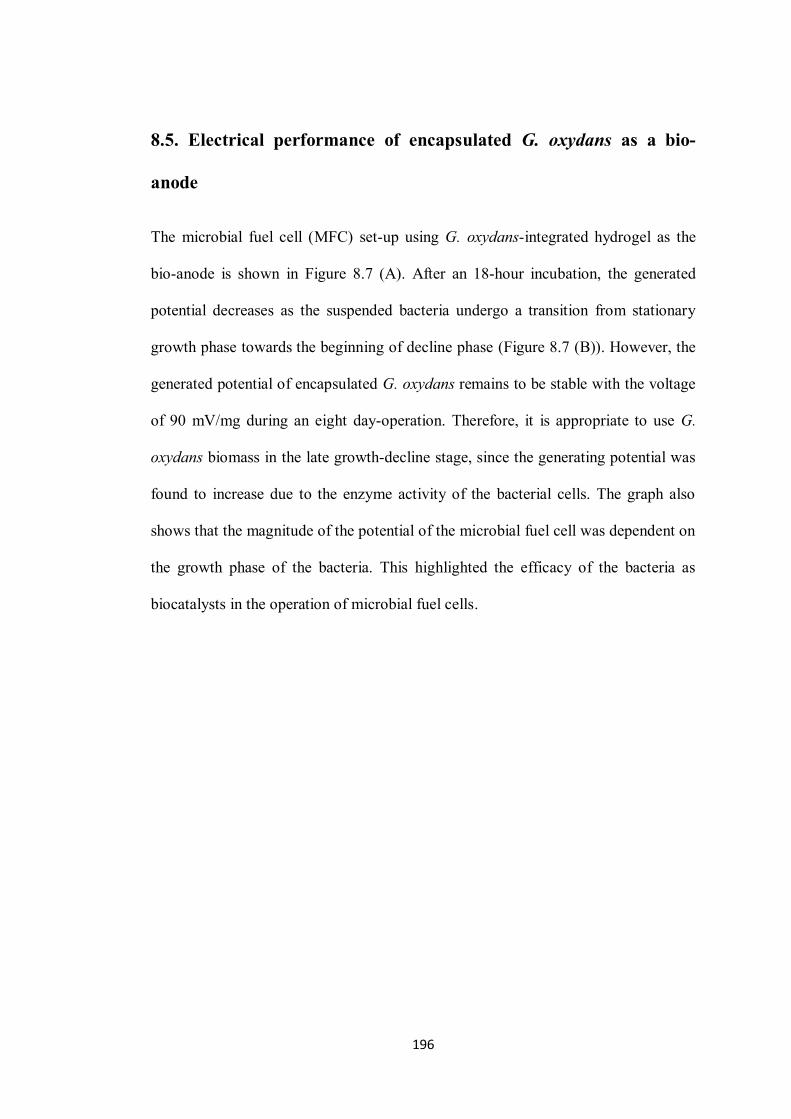
196
8.5. Electrical performance of encapsulated G. oxydans as a bio-
anode
The microbial fuel cell (MFC) set-up using G. oxydans-integrated hydrogel as the
bio-anode is shown in Figure 8.7 (A). After an 18-hour incubation, the generated
potential decreases as the suspended bacteria undergo a transition from stationary
growth phase towards the beginning of decline phase (Figure 8.7 (B)). However, the
generated potential of encapsulated G. oxydans remains to be stable with the voltage
of 90 mV/mg during an eight day-operation. Therefore, it is appropriate to use G.
oxydans biomass in the late growth-decline stage, since the generating potential was
found to increase due to the enzyme activity of the bacterial cells. The graph also
shows that the magnitude of the potential of the microbial fuel cell was dependent on
the growth phase of the bacteria. This highlighted the efficacy of the bacteria as
biocatalysts in the operation of microbial fuel cells.

197
Figure 8.7. Microbial fuel cell (MFC) performance analysis. ((A) Schematic of microbial fuel cell set-up, and (B) The long-term stability of encapsulated G. oxydans showing the electricity generation.
The power production characteristics of G. oxydans bacteria in suspension and in
their PVA-VP hydrogel encapsulated states are shown in Table 8.1. A comparative
analysis clearly highlighted that the microbial fuel cell developed with encapsulated
bacterial cells lead to an enhanced performance of the cell. There was almost a two-

198
fold increase in the generated voltage potential in the encapsulated state, compared
to the performance of the bacterial in their pristine state. Encapsulated G. oxydans
requires only 20-30 mins to generate 90.0 mV/mg of voltage while suspended
bacteria can only produce 48.0 mV/mg after 60-70 mins. In particular, resistance of
encapsulated G. oxydans is three-time lower than suspended bacteria, i.e. electron
conductivity of encapsulated G. oxydans is much higher than suspended bacteria.
From the data presented in Table 8.1, it can be seen that the formation of the micro-
wires by the electro-active bacteria with the hydrogel clearly augmented the electron
transfer from the redox centre of the cells to the electrode, compared to the situation
where the bacterial cells were present in their pristine state.
Table 8.1. Power production characteristics of G. oxydans bacteria-based biofuel cell in their suspended and L-PVA-VP encapsulated states.
8.6. Summary
To the best of our knowledge this is the first study that reports the self-organization
of G. oxydans cells into a biowire network by actively utilizing the properties of a
PVA-VP hydrogel system in which it is contained. A few examples are available
that have reported the formation of self-oriented electroactive cells. These include
the pili or pili-like nanowire formation by Shewanella oneidensis (Reguera et al.,
Type of biocatalyst
Generated potential, mV/mg of bacterial cells
Time for maximum potential generation,
(min)
Internal resistance,
(kΩ) Suspended
bacterial cells 48 60-70 300
Encapsulated bacterial cells
90 25-30 100

199
2005, Pirbadian et al., 2014, Gorby et al., 2006) and filamentous bacteria of the
family Desulfobulbaceae, which exhibit cable-like structures (Marzocchi et al.,
2014, Pfeffer et al., 2012). It was also described that non-electroactive bacteria such
as Lactobacillus fermentus and Bifidobacterium breve have been able to align
themselves to sense an external magnetic field after being coated with maghemite
nanoparticles (Martín et al., 2014). In addition, some artificial systems have been
developed to mediate the aggregation of non-electroactive bacteria using the cell
self-assembly of polymers (Drachuk et al., 2015, Sankaran et al., 2015)
Here, it was found that the self-organisation of G. oxydans was not due to changes in
pH as was reported for Helicobacter pyroli, which took place in to allow the
bacterial cells to propel themselves through the elevation of the pH of stomach
mucin hydrogel, or in the (Celli et al., 2009).formation of micro-colonies associated
with the polymeric chains, as found for Bacillus subtilis or Pseudomonas fluorescens
cells in polyacrylate polymeric systems (Truong et al., 2015, Quiles et al., 2012). In
contrast, G. oxydans biowires were composed of an extended network of bacterial
cells, which are side-by-side aligned. This orientation most likely facilitates efficient
electron transfer in order to minimize the interaction energy. So far, a similar side-
by-side alignment has only been reported for non-biological ellipsoidal micro-
particles (Botto et al., 2012). The alignment of the G. oxydans cells in the polymeric
hydrogel allowed microbial fuel cells containing them to generate a greater electric
potential than that obtained by suspended G. oxydans cells in the absence of the
hydrogel. The power generation of the PVA-VP/G. oxydans system was found to be
stable for more than eight days. This process has the potential to be exploited in the
novel design of highly efficient electricity generation cells that utilize components of
industrial organic waste.

200
Chapter 9
General discussion and conclusions

201
9.1. Overview
Fabrication of micro/nanostructures remains an area of high research priority due to the
technique having the capability for fabricating functional devices that will have a positive
impact on society (Brodie and Muray, 2013, Chen and Pepin, 2001, Gates et al., 2004).
Applications of these techniques include the fabrication of micro/nanostructures such as
one-dimensional nanotubes, two-dimensional graphene, and three-dimensional polymeric
networks. These structures have been fabricated via various techniques and have been
used in modern day biomedical industry applications (Geim and Novoselov, 2007,
Hernández-Vélez, 2006, Fujii and Enoki, 2012). Although extensive research efforts have
been invested and significant progress has been made in this area, the formation and
control of accurately produced nano-scale structures still faces significant challenges.
In this thesis, the nano-fabrication techniques used to create some of the commonly used
metallic, non-metallic and polymer surfaces have been discussed. The surface nano-
patterns resulting from these nano-fabrication techniques were characterised. The
mechanisms responsible for the antibacterial behaviour of these surfaces were found to
be due to their surface features, with the spatial arrangement of these surface structures
contributing significantly to their performance in biomedical industry applications.
Furthermore, it was found that the amount of air trapped between the nanostructures of
the surface can influence the position at which the bacterial cells will sit on the surface.
The bacterial cells coming into contact with the nano-structured surface become ruptured
in a similar manner to those observed in previous studies reporting the mechano-
bactericidal activity of cicada and dragonfly wings (Ivanova et al., 2012a, Pogodin et al.,
2013, Truong et al., 2012). The acquired knowledge regarding the significance of
entrapped air within a surface contributing to the antibacterial activity of that surface has
been used to synthesize artificial surfaces that allow a degree of control over the extent of

202
bacterial attachment. As an outcome, it was found that the surface topology at the
micron- and nano-scale is of paramount importance in determining the extent of
occurring bacterial attachment. A polymer mesoporous network was shown to play a
crucial role in favouring the release of electrons from G. oxydans cells by allowing the
cells to form a three-dimensional network within the polymer chains. The bacteria-
polymer network was also found to enhance the power and current density of a microbial
fuel cell compared to that obtained using a conventional microbial fuel cell.
9.2. Bactericidal “smart” materials and their applications
The design, fabrication and functionality of antibacterial titanium surfaces have been
discussed in Chapter 4. Titanium nano-patterned arrays were fabricated on a
commercially pure titanium surface via a chemical hydrothermal treatment using alkaline
KOH as the working solution. The presence and distribution of the resulting nano-arrays,
induced by liquid hydrothermal treatment, were analysed using optical profilometry
imaging techniques. The SEM micrographs of the surface revealed that the micron-scale
surface topography was not altered by the hydrothermal etching, however arrays of nano-
wires arrays were observed to form on the surface. A comparative roughness analysis
was performed using two conventional surface roughness parameters, the average
roughness (Sa) and the root mean square roughness (Sq) (Webb et al., 2012, Gadelmawla
et al., 2002). These parameters showed that the nano-roughness of the nano-patterned Ti
was greater than that of the as-received sample due to the formation of the nanowire
arrays. Also, wettability analysis of both surfaces revealed that the nano-patterned
surface was more hydrophobic compared to that of the as-received sample, due to the
presence of air bubbles in the spaces between the nano-wires (Truong et al., 2012, Sheng
and Zhang, 2011).

203
Hydrothermal treatment has been previously employed for the generation of nano-
patterns because this technique has the ability to produce desired features under
controlled experimental conditions (Diu et al., 2014, Kim et al., 2013a). The autoclave
temperature, pressure, time of the reaction and post-treatment washing steps are
important parameters that determine the formation of the nano-features on a surface (Tsai
and Teng, 2006, Kasuga et al., 1998, Kasuga et al., 1999, Pookmanee et al., 2004). It has
been recognized that the treatment of titanium oxide with concentrated alkali solutions at
high temperatures leads to the disruption of some of the Ti-O bonds, forming lamellae-
like fragments, which are an intermediary step in the formation of nanotubes and
nanowires. These lamellae/nanosheets are gradually rolled up into nanowires or
disintegrate into nano-wire-like arrays with the application of increased temperature and
pressure (Kukovecz et al., 2005, Wu et al., 2006). An increase in the temperature range
has also been associated with the increase in the length and width of the nano-wires that
are formed (Ou and Lo, 2007). These nano-patterns have also been found to be a function
of the alkali precursor used; nanoribbons have been formed at NaOH concentrations of
5–15 N under temperature range of 180–250C, which was assigned for the
H2Ti5O11.H2O phase, while nanowires are formed at the solution of KOH and indexed as
K2Ti8O7 (Seo et al., 2001, Yuan and Su, 2004, Mao et al., 2006). Acid washing of these
nano-patterns has also been reported, performed mainly for the ion-exchange process,
although this step is not optional and hence, has not been carried out in this work (Du et
al., 2001, Lan et al., 2005). The parameters associated with hydrothermal treatment
make it a desirable process for the up-scaled fabrication of complex geometries atop
metallic surfaces.
The nano-patterned arrays were found to show selective bactericidal activity by
eliminating ~ 50% of Pseudomonas aeruginosa and ~ 20% of Staphylococcus aureus

204
bacterial cells. The nano-patterns were found to be more effective in eliminating the
attachment of Gram-negative P. aeruginosa cells, as these cells are devoid of the
extracellular peptidoglycan layer possessed by the Gram-positive S. aureus cells. A
similar result has been also observed on cicada and dragonfly wings (Hasan et al., 2013b,
Ivanova et al., 2013a, Ivanova et al., 2012a, Nowlin et al., 2015). The authors showed
that the forces imparted to the bacterial cells are mostly mechanical in nature. the
bactericidal behaviour is, therefore a function of the efficiency with which the nano-
structures can rupture the bacterial cell membranes.
An interface exists where an implant surface comes into contact with eukaryotic cell
lines, with the cells and the substrate considered as two separate entities. This interface
monitors the exchange of information, as the cells can infer the signals received from the
substrate and allow the bacteria to decide the further course of interaction that is
dependent on the mechanical, physical and chemical properties of the substratum. A
healthy level of osseo-integration within the nano-patterned Ti surface and primary
fibroblasts (pHF) was demonstrated in Chapter 5. After 10 days of incubation, the pHF
cells formed a 90% confluent monolayer on the as-received surfaces, whereas multiple
layers of cells were observed, using both SEM and CLSM, on the nano-patterned
surfaces. While the pHF cells on the AR-Ti surfaces were found to be evenly distributed
and elongated over the 10-day incubation period, the cells were found to exhibit an
extended morphology on the HTE-Ti surfaces. This different attachment morphology
was attributed to the nano-wire aligned attachment behaviour of the pHF cells on the
HTE-Ti surfaces. Previously, authors have reported that factors such as surface
hydrophobicity, surface topology and surface roughness play an important role in guiding
the growth and the proliferation of eukaryotic cells (Ross et al., 2012, Loesberg et al.,
2007, Bettinger et al., 2009, Lord et al., 2010). A single cell, upon interaction with the

205
nano-scaled topology, reviews its surroundings and moves using nanometre scale
developments such as filopodia and lamellipodia. The filopodia serve as anchor points
for cellular proliferation, as seen in Figure 9.1. As these structures have sizes in the
nanometre range (250–400 nm) the chances that they will be influenced by the nano-
topography of the substrate surface are very high (McClay, 1999, Dalby et al., 2007,
Partridge and Marcantonio, 2006). It has also been observed that these nano-sized
filopodia produce focal adhesion points after reviewing their surroundings and then tend
to migrate with the extension of cell protrusions (Anselme et al., 2010, Lord et al., 2010,
Teixeira et al., 2003, Dalby et al., 2006). It should be noted that the formation of focal
adhesion points depends mainly on the quality of the grooves formed on the surface
(Fujita et al., 2009, Dalby, 2005, Dalby et al., 2004). The directionality of the focal
adhesion also plays an important role; focal adhesion points that are formed along the
nano-sized grooves are more stable than the adhesion points that are grown in an
orthogonal direction over the grooves or ridges on the surface (Parker et al., 2002,
Lamers et al., 2012, Klymov et al., 2013). Hence, it was inferred that surface nano-
topography affects the shape and assemblage of focal adhesion points and that the
presence of nano-scaled features is crucial for the success of the implant system inside
the physiological environments for a prolonged life-span.

206
Figure 9.1. A schematic representation of the proposed design of nano-pillar arrays for guiding cell behaviour. (A) (A-D) Steps showing lithographic fabrication of nano-pillars to provide specific geometry and spacing, surface functionalization of the NPs to address cell adhesion sites, control of the mechanical properties of NPs by changing the fabrication parameters and nano-pillar actuation to stimulate cells or to detect forces exerted by cells on NPs. (E) cross-sectional SEM image of a representative stem cell proliferation and attachment on nano-pillared surface. Scale bar is 200 nm. (B) Schematic representation of cell proliferation elucidating the importance of spacing and symmetry of high-aspect-ratio NP arrays, where red indicates areas of cell adhesion. Cell spreading initiates at early (A) and late (B, C) stages of cell spreading. On high-density NP arrays where p < dcrit (critical distance), the filopodia establish focal adhesions with the surface in all directions. On medium-density NPs at distances between the NPs reaching dcrit, only extensions oriented in the lattice directions will be able to find the adhesion, while extensions growing in other directions will be unable to bridge the gap > dcrit. On low-density NP arrays where p> dcrit, cells can no longer bridge the pillars in any direction; cells penetrate to the underlying substrate and extend at the floor of the nano-forest. (Adapted with permission from (Bucaro et al., 2012)).
A systematic study towards understanding how the modulation of the nano-pattern may
dramatically control the extent of the bactericidal activity was performed and discussed
in Chapter 6. Black silicon is a commonly studied artificial substrate, whose bactericidal
effect has been previously determined (Ivanova et al., 2013a). A deeper understanding of
207
the interaction between nano-pillared bSi surfaces with bacterial cells revealed that the
geometry of the nano-pillars was instrumental in determining the fate of the cells when
they make first contact with the pillared surface. A pillar height of ~600 nm and width of
~100 nm was found to be an appropriate geometrical parameter range for effective
bactericidal performance. Looking at the natural analogues, it was postulated earlier that
the bacterial cells were ruptured due to physical stretching and damage by the pillars on
the cicada and dragonfly wings. These studies were, however, not exhaustive in that they
did not provide a distinct demonstration of the factors responsible for the physical
deformation of the cells upon landing on the pillars (Pogodin et al., 2013, Hasan et al.,
2013b). The most important attributes of the nano-pillars regulating bacterial interaction
have been determined to be the height, width and density of the pillars. To act as a
successful bactericidal surface as found on cicada wings, a theoretical study was reported
that the pillar height should be ~200 nm, width be ~ 70 nm and the pillars should have a
densely packed configuration (Xue et al., 2015, Kelleher et al., 2015). This arrangement
of the pillars not only prevents the bacterial cells from settling down into the recesses
between the pillars but also helps in eliminating the cells by piercing and damaging the
cell membrane. The study has contributed in the further understanding of the importance
of the nano-scaled geometric patterns towards regulating bacterial attachment on any
surface.
The effects of the bactericidal activity of the nano-pillared black silicon surfaces in
dynamic conditions were reported in Chapter 7. The bactericidal activity of the black
silicon surfaces was maintained inside a three dimensional microfluidic channel, and was
able to eliminate pathogenic bacterial cells from an aqueous solution. From this study,
the presence of a total cellular protein yield could be evaluated from the analyte. A
narrow 15 μm high and 1 cm wide flat flow channel was constructed that allowed the

208
bacteria to come into contact with the bactericidal nano-spikes present on the surface of
the bSi. The narrow channel within the device was designed so that a single layer of
bacterial cells could reside at any given time above the bSi substratum during flow. The
large 1 × 2 cm2 surface area of the bSi was shown to be efficient in being able to kill
Pseudomonas aeruginosa cells, achieving an approximate 99% killing efficiency. The
incorporation of the bactericidal surface inside the channel minimized the working steps
used in the identification of the extra cellular contents via microfluidics as conventional
microfluidics studies frequently use FRET, 2D mass-spectrometry, 2D electrophoresis or
laborious immunostaining techniques used previously to achieve the same result (Lin et
al., 2014, Shameli and Ren, 2015, Gao et al., 2013, Mellors et al., 2013). These extra
steps are not only time-consuming, but they also increase the fabrication costs and
complicate experimental designs, resulting in time lags in achieving the desired results,
as shown in Figure 9.2.
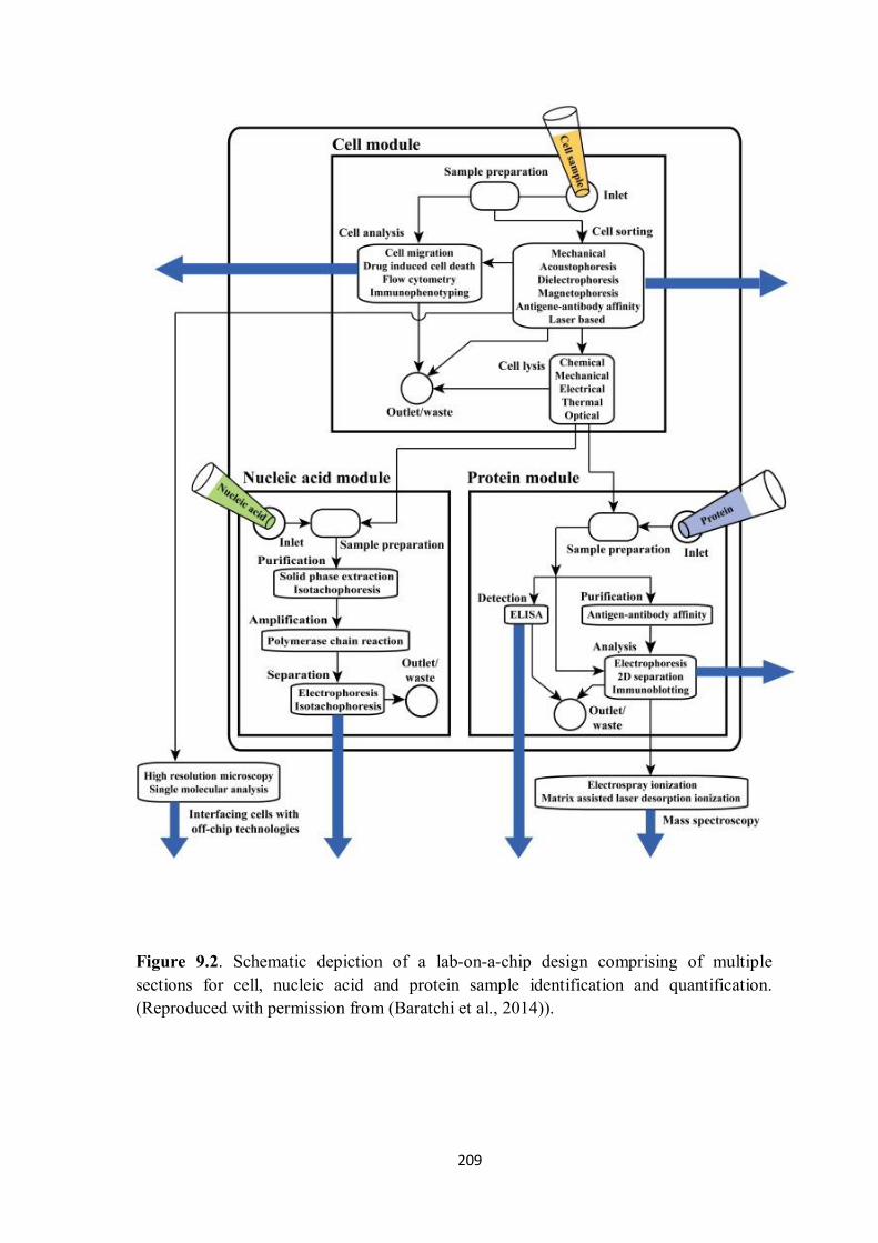
209
Figure 9.2. Schematic depiction of a lab-on-a-chip design comprising of multiple sections for cell, nucleic acid and protein sample identification and quantification. (Reproduced with permission from (Baratchi et al., 2014)).

210
These additional steps also depend on the accessibility of antibody conjugates to bind to
target proteins, and require at-least 10 to 100 μL of the sample (Hauss and Müller, 2007).
The experimental protocols developed in the current study helped to simplify the steps as
the nano-pillared surface helped to lyse the cell. The resulting cellular protein content
was analysed by a facile Bradford’s assay (Zor and Selinger, 1996, Kruger, 1994,
Bradford, 1976). Complete rupturing of E. coli cells was achieved after 15 cycles,
allowing the effective release of cellular proteins from within the bacterial cells (65.2
μg/mL from 3 × 10⁸ cells/mL). The fabrication and generation of such a microfluidic
device can not only be used as a platform to cause lysis of bacterial, viral and eukaryotic
cells, but can also be used as a convenient measurement tool for the analysis of
extracellular components. The parameters of the channel, such as the flow rate, height
and width, have been designed in such a manner that they can be easily re-optimized to
accommodate any other varieties of cellular components.
9.3. Construction of 3D environments for exoelectrogenic bacteria
The interaction of three dimensional polymeric PVA-VP networks with electron
conducting Gluconobacter oxydans was reported in Chapter 8. This study was inspired
from the fundamental aspect of Gram-negative prokaryotic cells, which have respiratory
redox proteins located in the cell membrane and reachable from the periplasm (Tkac et
al., 2003, Vostiar et al., 2004). The outer membrane contains porins, which makes it
permeable for a wide variety of low molecular-weight charged mediators. The
periplasmic membrane bound pyrroloquinoline quinone (PQQ), containing enzymes of
these genera, provide fast and highly efficient oxidation of a wide variety of substrates

211
(Reshetilov et al., 1998a, Reshetilov et al., 1998b, Tkac et al., 2003). It has been reported
that G. sulfurreducens and S. oneidensis bacteria have the ability to form electrical
nanowires in the presence of an osmium nanowires. These nanowires have been formed
by the combination of redox polymers and electron mediators such as glucose,
ferricyanide, dichlorphenolindophenol, viologens or quinones, which act as effective
mediators for membrane bound PQQ dependent dehydrogenases (Tkac et al., 2009,
Delaney et al., 1984, Wang, 2008, Chaudhuri and Lovley, 2003). These nanowires can
also be formed from the type IV pili of the motile electron-conducting organisms. The
cells arrange themselves in a linear fashion which makes electron transfer feasible from
one cell to another, with an assumption that the cytochromes are aligned along the
filament with a minimum spacing of 0.7 nm to allow sufficient electron coupling
(Reguera et al., 2005, Reguera et al., 2007, Albers and Pohlschröder, 2009, Shi et al.,
2007). External electron transfer has been divided into two categories: direct and indirect
electron transfer. Direct electron transfer mainly incorporates the use of redox active
proteins such as c-type cytochromes and filamentous apparatus to aid in electron transfer.
On the other hand, indirect electron transfer comprises of the generation of phenazine
compounds and flavin derivatives which act as electron mediators (Kato, 2015, Peng et
al., 2010a, Marsili et al., 2008, Pirbadian et al., 2014, Gorby et al., 2006). It was observed
in this study, however, that the electron conducting cells of non-motile Gluconobacter
oxydans have the ability to transfer electrons by forming self-aligned micro-wires that
disrupt the three dimensional polymeric hydrogel network, which has not previously
been observed. G. oxydans showed a strong tendency to interact with the mesoporous,
three-dimensional PVA-VP hydrogel network and align itself in a chain-like
configuration. It can be assumed that the electron transfer was solely due to the ability of
the bacteria to self-orient as a bio wire, while being able to disrupt the polymeric

212
network. The self-alignment of the bacterial cells into short and long chains in the PVA
hydrogel network served two purposes: the system helped to increase the power density
of the microbial fuel cell and has increased the longevity of the bio-electrode by as much
as 7 days.
9.4. Summary and conclusions
An important element for studying cell-nanoenvironment interactions is to design,
characterize and influence forceful environmental cues in vitro inside a cellular (micron)
and sub-cellular (nano) length scale. These substrata have simplified cell biology studies
for health applications and have provided the means for engineers, material scientists and
biologists to combine forces. The last two decades have seen a range of micro/nano-
engineering tools and fabrication methods for functionalized materials, which have been
utilised in biological and biomedical research. Advances have also been made in the
fabrication of functional materials with different nanoscale cues that mimic individual
aspects of the in vivo cell environment. From the standpoint of vital science, these nano-
engineered surfaces have uncovered innovative mechano-sensitive and responsive
cellular behaviours and allowed the underlying mechano-transduction mechanisms to be
identified. The fabrication of multidimensional functional materials needs further
investigation to provide a conjoined platform for the collaborative performance of 2-
dimensional and 3-dimensional surfaces.
Commercially pure titanium was shown to be covered by a dense array of nano-patterns
after being subjected to a liquid hydrothermal treatment, very similar to the layer of
nano-pillars found on dragonfly wings. These nano-patterned arrays were found to
directly influence a number of properties, i.e. superhydrophobicity, self-cleaning and
bactericidal activities of the titanium surface. The nano-patterned arrays were mostly

213
found to be composed of the anatase form of titanium oxide and were moderately
bactericidal towards Pseudomonas aeruginosa and Staphylococcus aureus bacterial cells.
The topology of the surface also acted as a guided medium for the primary human
fibroblasts to elongate and proliferate over a 10-day period.
The precise geometrical parameters of the nano-pillars of black silicon surfaces were
shown to be the crucial factors that determined their wettability and subsequently their
bactericidal activities. The surface topographies of black silicon surfaces were
characterised and compared to identify the correlation between surface topography and
bactericidal activity. It was found that minor differences in the pillar geometries such as
the pillar height, density and aspect ratio could switch the performance of the surfaces
from being a modest to a strong bactericidal surface, and it is postulated here that surface
topology plays a significant role in controlling these mechanisms. Slightly increased
pillar height and density tended to result in more effective bactericidal activity and cell
rupture.
Having gained an understanding of the contributions of surface topography on the
bactericidal activity of black silicon surfaces in static conditions, bactericidal activity in
dynamic conditions was tested by embedding black silicon in a microfluidic device. The
black silicon chip proved to be bactericidal in dynamic conditions, killing ~99 % of P.
aeruginosa cells in suspension. The bactericidal activity of the bSi chip in dynamic flow
was found to depend upon two conditions: the flow rate of the bacterial suspension
solution and the time of interaction of the chip with the nano-pillared surface.
The interaction of bacterial cells with three dimensional surfaces was further understood
by investigating the interaction of G. oxydans cells with a PVA hydrogel network. G.
oxydans are electro-active bacterial cells, capable of external electron transfer. A three-

214
dimensional PVA hydrogel was designed to examine the ability of the cells to transfer
electrons, while being held in a polymeric network. An important conclusion was
observed: G. oxydans transferred electrons by forming chains while interacting with the
hydrogel system and distorted the original polymeric structure (as proposed in this work
for the first time). This novel hydrogel-bacterial mesh was also found to enhance the
power production in a MFC and increased the longevity of the cell by up to 7 days.

215
Chapter 10
Future directions

216
10.1. Future scope of this work
While the current work has generated useful knowledge regarding the fabrication of
multidimensional surfaces, together with their behaviour with bacterial and
eukaryotic cells and initial applications, the following work is still needed to
successfully allow the up-scale of the technology for real-world applications.
Further optimization of the hydrothermal treatment for fabricating titanium nano-
structured surfaces could lead to a surface with enhanced bactericidal activities. With
the correct selection of parameters such as the reaction time, concentration of the
alkalinity of the working solution and heat treatments of the titanium surfaces, it may
be possible to produce a precise structure with greater killing activity than that found
on the surface of dragonfly wings.
Black silicon surfaces have been shown to have a moderate bactericidal activity
against commonly found pathogens such as Pseudomonas aeruginosa and
Staphylococcus aureus. The bactericidal activity could be further improved if the
geometrical parameters of the nano-pillars such as the density, height and the aspect
ratio of the nano-pillars could be accurately monitored so that any slight variations in
the nano-scale could be avoided, with an aim to attain 100 % bactericidal efficiency.
The bactericidal activity of black silicon surface under dynamic conditions has also
been tested in this work. The use of a bSi surface embedded in a microfluidic
channel to kill bacterial cells was reported for the first time. The applications of this
channel could further be optimized and unscaled to test the interaction of eukaryotic
cells in fluid state with the nano-pillared surface by optimizing the channel design
parameters such as the flow rate of the solution and the height of the channel.
Optimization of the channel to analyse samples such as blood, urine and other real-
life samples could also be evaluated in future work.

217
10.2. Final Remarks
This thesis explains the potential applications of multidimensional surfaces in the field of
implant science, microbial fuel cells and microfluidics. With further optimization of the
process and design parameters, new innovative structured surfaces can be designed and
their potential be maximised for greater usage in science and technology.

218
BIBLIOGRAPHY

219
ABRAMOWITZ, S. 1999. DNA analysis in microfabricated formats. Biomedical Microdevices, 1, 107-112.
ABRON, A., HOPFENSPERGER, M., THOMPSON, J. & COOPER, L. F. 2001. Evaluation of a predictive model for implant surface topography effects on early osseointegration in the rat tibia model. The Journal of Prosthetic Dentistry, 85, 40-46.
ADDEN, N., GAMBLE, L. J., CASTNER, D. G., HOFFMANN, A., GROSS, G. & MENZEL, H. 2006. Phosphonic acid monolayers for binding of bioactive molecules to titanium surfaces. Langmuir, 22, 8197-8204.
ADIGA, S. P., JIN, C., CURTISS, L. A., MONTEIRO‐RIVIERE, N. A. & NARAYAN, R. J. 2009. Nanoporous membranes for medical and biological applications. Wiley Interdisciplinary Reviews: Nanomedicine and Nanobiotechnology, 1, 568-581.
AGARWAL, S., WENDORFF, J. H. & GREINER, A. 2008. Use of electrospinning technique for biomedical applications. Polymer, 49, 5603-5621.
AHMED, H. 1997. Single electron electronics: Challenge for nanofabrication. Journal of Vacuum Science & Technology B, 15, 2101-2108.
AI, B., YU, Y., MÖHWALD, H., ZHANG, G. & YANG, B. 2014. Plasmonic films based on colloidal lithography. Advances in Colloid and Interface Science, 206, 5-16.
AIZAWA, M. & BURIAK, J. M. 2005. Block copolymer-templated chemistry on Si, Ge, InP, and GaAs surfaces. Journal of the American Chemical Society, 127, 8932-8933.
AIZAWA, M. & BURIAK, J. M. 2006. Nanoscale patterning of two metals on silicon surfaces using an ABC triblock copolymer template. Journal of the American Chemical Society, 128, 5877-5886.
AKBARZADEH, A., SAMIEI, M. & DAVARAN, S. 2012. Magnetic nanoparticles: preparation, physical properties, and applications in biomedicine. Nanoscale Research Letters, 7, 1-13.
AKHMANOVA, M., OSIDAK, E., DOMOGATSKY, S., RODIN, S. & DOMOGATSKAYA, A. 2015. Physical, spatial, and molecular aspects of extracellular matrix of in vivo niches and artificial scaffolds relevant to stem cells research. Stem Cells International, 2015.

220
AL-KINDI, G. A. & SHIRINZADEH, B. 2007. An evaluation of surface roughness parameters measurement using vision-based data. International Journal of Machine Tools and Manufacture, 47, 697-708.
ALBERS, S.-V. & POHLSCHRÖDER, M. 2009. Diversity of archaeal type IV pilin-like structures. Extremophiles, 13, 403-410.
ALFEROV, S. V., MINAICHEVA, P. R., ARLYAPOV, V. A., ASULYAN, L. D., ALFEROV, V. A., PONAMOREVA, O. N. & RESHETILOV, A. N. 2014. Bioanode for a microbial fuel cell based on Gluconobacter oxydans immobilized into a polymer matrix. Applied Biochemistry and Microbiology, 50, 637-643.
ALLEN, R. D., BROCK, P. J., SUNDBERG, L., LARSON, C. E., WALLRAFF, G. M., HINSBERG, W. D., MEUTE, J., SHIMOKAWA, T., CHIBA, T. & SLEZAK, M. 2005. Design of protective topcoats for immersion lithography. Journal of Photopolymer Science and Technology, 18, 615-619.
ALTUNAKAR, B. & KOKINI, J. 2016. Fabrication of biodegradable zein films by using soft lithography. Une, 13, 15.
AMATO, G., DELERUE, C. & VONBARDELEBEN, H. 1998. Structural and optical properties of porous silicon nanostructures, CRC Press.
ANDERSSON, D. I. 2003. Persistence of antibiotic resistant bacteria. Current Opinion in Microbiology, 6, 452-456.
ANDERSSON, H. & VAN DEN BERG, A. 2004. Microfabrication and microfluidics for tissue engineering: state of the art and future opportunities. Lab Chip, 4, 98-103.
ANGUS, S. J., FERGUSON, A. J., DZURAK, A. S. & CLARK, R. G. 2007. Gate-defined quantum dots in intrinsic silicon. Nano Letters, 7, 2051-2055.
ANPO, M. & KAMAT, P. V. 2010. Environmentally benign photocatalysts: applications of titanium oxide-based materials, Springer Science & Business Media.
ANSARI, K., VAN KAN, J., BETTIOL, A. & WATT, F. 2004. Fabrication of high aspect ratio 100 nm metallic stamps for nanoimprint lithography using proton beam writing. Applied Physics Letters, 85, 476-478.
ANSELME, K., DAVIDSON, P., POPA, A., GIAZZON, M., LILEY, M. & PLOUX, L. 2010. The interaction of cells and bacteria with surfaces structured at the nanometre scale. Acta Biomaterialia, 6, 3824-3846.

221
AO, X., TONG, X., KIM, D. S., ZHANG, L., KNEZ, M., MÜLLER, F., HE, S. & SCHMIDT, V. 2012. Black silicon with controllable macropore array for enhanced photoelectrochemical performance. Applied Physics Letters, 101, 111901.
APHAIRAJ, D., WIRUNMONGKOL, T., NIYOMWAS, S., PAVASUPREE, S. & LIMSUWAN, P. 2014. Synthesis of anatase TiO2 nanotubes derived from a natural leucoxene mineral by the hydrothermal method. Ceramics International, 40, 9241-9247.
ARAN, K., FOK, A., SASSO, L. A., KAMDAR, N., GUAN, Y., SUN, Q., ÜNDAR, A. & ZAHN, J. D. 2011. Microfiltration platform for continuous blood plasma protein extraction from whole blood during cardiac surgery. Lab on a Chip, 11, 2858-2868.
ARCIOLA, C. R., CAMPOCCIA, D., SPEZIALE, P., MONTANARO, L. & COSTERTON, J. W. 2012. Biofilm formation in Staphylococcus implant infections. A review of molecular mechanisms and implications for biofilm-resistant materials. Biomaterials, 33, 5967-5982.
ARIAS, C. A. & MURRAY, B. E. 2009. Antibiotic-resistant bugs in the 21st century—a clinical super-challenge. New England Journal of Medicine, 360, 439-443.
ARIGA, K., HILL, J. P. & JI, Q. 2007. Layer-by-layer assembly as a versatile bottom-up nanofabrication technique for exploratory research and realistic application. Physical Chemistry Chemical Physics, 9, 2319-2340.
ARIMA, Y., KATO, K., TERAMURA, Y. & IWATA, H. 2011. Design of biointerfaces for regenerative medicine. Polymers in Nanomedicine. Springer.
ARJMANDI, N., LAGAE, L. & BORGHS, G. 2009. Enhanced resolution of poly (methyl methacrylate) electron resist by thermal processing. Journal of Vacuum Science & Technology B, 27, 1915-1918.
ARMENTANO, I., ARCIOLA, C. R., FORTUNATI, E., FERRARI, D., MATTIOLI, S., AMOROSO, C. F., RIZZO, J., KENNY, J. M., IMBRIANI, M. & VISAI, L. 2014. The interaction of bacteria with engineered nanostructured polymeric materials: a review. The Scientific World Journal, 2014.
ARMSTRONG, A. R., ARMSTRONG, G., CANALES, J. & BRUCE, P. G. 2004. TiO2‐B nanowires. Angewandte Chemie International Edition, 43, 2286-2288.

222
ARORA, A., SIMONE, G., SALIEB-BEUGELAAR, G. B., KIM, J. T. & MANZ, A. 2010. Latest developments in micro total analysis systems. Analytical Chemistry, 82, 4830-4847.
ARSHAD, S. N., NARAGHI, M. & CHASIOTIS, I. 2011. Strong carbon nanofibers from electrospun polyacrylonitrile. Carbon, 49, 1710-1719.
ARYAL, M., TRIVEDI, K. & HU, W. 2009. Nano-confinement induced chain alignment in ordered P3HT nanostructures defined by nanoimprint lithography. ACS Nano, 3, 3085-3090.
ATHAWALE, V. & RATHI, S. 1997. Effect of chain length of the alkyl group of alkyl methacrylates on graft polymerization onto starch using ceric ammonium nitrate as initiator. European Polymer Journal, 33, 1067-1071.
AU, A. K., LEE, W. & FOLCH, A. 2014. Mail-order microfluidics: evaluation of stereolithography for the production of microfluidic devices. Lab on a Chip, 14, 1294-1301.
AVOURIS, P. & DIMITRAKOPOULOS, C. 2012. Graphene: synthesis and applications. Materials Today, 15, 86-97.
AWAJA, F., CARLETTI, E., BONANI, W. & SPERANZA, G. 2015. Vinculin focal adhesion of osteoblast‐like cells on PEEK coated with ultra‐thin polymer nano films. Journal of Applied Polymer Science, 132.
AYON, A., CHEN, K.-S., LOHNER, K., SPEARING, S., SAWIN, H. & SCHMIDT, M. Deep reactive ion etching of silicon. MRS Proceedings, 1998. Cambridge Univ Press, 51.
BABKINA, E., CHIGRINOVA, E., PONAMOREVA, O., ALFEROV, V. & RESHETILOV, A. 2006. Bioelectrocatalytic oxidation of glucose by immobilized bacteria Gluconobacter oxydans. Evaluation of water-insoluble mediator efficiency. Electroanalysis, 18, 2023-2029.
BABOROWSKI, J. 2004. Microfabrication of piezoelectric MEMS. Integrated Ferroelectrics, 66, 3-17.
BAKER, M. I., WALSH, S. P., SCHWARTZ, Z. & BOYAN, B. D. 2012. A review of polyvinyl alcohol and its uses in cartilage and orthopedic applications. Journal of Biomedical Materials Research Part B: Applied Biomaterials, 100, 1451-1457.
BANERJEE, S., DIONYSIOU, D. D. & PILLAI, S. C. 2015. Self-cleaning applications of TiO2 by photo-induced hydrophilicity and photocatalysis. Applied Catalysis B: Environmental, 176, 396-428.

223
BARATCHI, S., KHOSHMANESH, K., SACRISTÁN, C., DEPOIL, D., WLODKOWIC, D., MCINTYRE, P. & MITCHELL, A. 2014. Immunology on chip: Promises and opportunities. Biotechnology Advances, 32, 333-346.
BARTONA, S. C. & ATANASSOV, P. 2004. Enzymatic biofuel cells for implantable and micro-scale devices. Preprint Papers–American Chemical Society, Division of Fuel Chemistry, 49, 476.
BARUAH, S. & DUTTA, J. 2009. Nanotechnology applications in pollution sensing and degradation in agriculture: a review. Environmental Chemistry Letters, 7, 191-204.
BAT, E., LEE, J., LAU, U. Y. & MAYNARD, H. D. 2015. Trehalose glycopolymer resists allow direct writing of protein patterns by electron-beam lithography. Nature Communications, 6.
BAUER, A., LAYH, N., SYLDATK, C. & WILLETTS, A. 1996. Polyvinyl alcohol-immobilized whole-cell preparations for the biotransformation of nitriles. Biotechnology Letters, 18, 343-348.
BAVYKIN, D. V. & WALSH, F. C. 2010. Titanate and titania nanotubes: synthesis, properties and applications, Royal Society of Chemistry.
BAYATA, F., SARUHAN-BRINGS, B. & ÜRGEN, M. 2014. Hydrogen gas sensing properties of nanoporous Al-doped titania. Sensors and Actuators B: Chemical, 204, 109-118.
BAZAKA, K., JACOB, M. V., CRAWFORD, R. J. & IVANOVA, E. P. 2012. Efficient surface modification of biomaterial to prevent biofilm formation and the attachment of microorganisms. Applied Microbiology and Biotechnology, 95, 299-311.
BEATTIE, D. A., BEAUSSART, A., MIERCZYNSKA-VASILEV, A., HARMER, S. L., THIERRY, B., PUSKAR, L. & TOBIN, M. 2012. Synchrotron FTIR microscopy of Langmuir–Blodgett monolayers and polyelectrolyte multilayers at the solid–solid interface. Langmuir, 28, 1683-1688.
BEAUSSART, A., PETRONE, L., MIERCZYNSKA-VASILEV, A., MCQUILLAN, A. J. & BEATTIE, D. A. 2012. In situ ATR FTIR study of dextrin adsorption on anatase TiO2. Langmuir, 28, 4233-4240.
BECK, M., GRACZYK, M., MAXIMOV, I., SARWE, E.-L., LING, T., KEIL, M. & MONTELIUS, L. 2002. Improving stamps for 10 nm level wafer scale nanoimprint lithography. Microelectronic Engineering, 61, 441-448.
BECKER, H. & LOCASCIO, L. E. 2002. Polymer microfluidic devices. Talanta, 56, 267-287.

224
BEN-ZE'EV, A., FARMER, S. R. & PENMAN, S. 1980. Protein synthesis requires cell-surface contact while nuclear events respond to cell shape in anchorage-dependent fibroblasts. Cell, 21, 365-372.
BENECKE, B.-J., BEN-ZE'EV, A. & PENMAN, S. 1978. The control of mRNA production, translation and turnover in suspended and reattached anchorage-dependent fibroblasts. Cell, 14, 931-939.
BENZ, C., RETZBACH, H., NAGL, S. & BELDER, D. 2013. Protein–protein interaction analysis in single microfluidic droplets using FRET and fluorescence lifetime detection. Lab on a Chip, 13, 2808-2814.
BESLING, W., GOOSSENS, A., MEESTER, B. & SCHOONMAN, J. 1998. Laser-induced chemical vapor deposition of nanostructured silicon carbonitride thin films. Journal of Applied Physics, 83, 544-553.
BETTINGER, C. J., LANGER, R. & BORENSTEIN, J. T. 2009. Engineering substrate topography at the micro‐and nanoscale to control cell function. Angewandte Chemie International Edition, 48, 5406-5415.
BEVERIDGE, T. J. 1999. Structures of gram-negative cell walls and their derived membrane vesicles. Journal of Bacteriology, 181, 4725-4733.
BHAGAT, J. K. 1991. Miniature inductor for integrated circuits and devices. Google Patents.
BHARDWAJ, J., ASHRAF, H. & MCQUARRIE, A. Dry silicon etching for MEMS. Proc. Symp. Microstructures and Microfabricated Systems, ECS, 1997. 1-13.
BHARDWAJ, N. & KUNDU, S. C. 2010. Electrospinning: a fascinating fiber fabrication technique. Biotechnology Advances, 28, 325-347.
BHUSHAN, B. 2009. Biomimetics: lessons from nature–an overview. Philosophical Transactions of the Royal Society of London A: Mathematical, Physical and Engineering Sciences, 367, 1445-1486.
BHUSHAN, B. & JUNG, Y. C. 2011. Natural and biomimetic artificial surfaces for superhydrophobicity, self-cleaning, low adhesion, and drag reduction. Progress in Materials Science, 56, 1-108.
BHUSHAN, B., JUNG, Y. C. & KOCH, K. 2009. Self-cleaning efficiency of artificial superhydrophobic surfaces. Langmuir, 25, 3240-3248.
BIELA, S. A., SU, Y., SPATZ, J. P. & KEMKEMER, R. 2009. Different sensitivity of human endothelial cells, smooth muscle cells and fibroblasts to topography in the nano–micro range. Acta Biomaterialia, 5, 2460-2466.

225
BISWAS, A., BAYER, I. S., BIRIS, A. S., WANG, T., DERVISHI, E. & FAUPEL, F. 2012. Advances in top–down and bottom–up surface nanofabrication: Techniques, applications & future prospects. Advances in Colloid and Interface Science, 170, 2-27.
BIXLER, G. D. & BHUSHAN, B. 2015. Rice and butterfly wing effect inspired low drag and antifouling surfaces: A review. Critical Reviews in Solid State and Materials Sciences, 40, 1-37.
BLOSSEY, R. 2003. Self-cleaning surfaces—virtual realities. Nature Materials, 2, 301-306.
BORENSTEIN, J. T., TERAI, H., KING, K. R., WEINBERG, E., KAAZEMPUR-MOFRAD, M. & VACANTI, J. 2002. Microfabrication technology for vascularized tissue engineering. Biomedical Microdevices, 4, 167-175.
BORGES, J. O. & MANO, J. F. 2014. Molecular interactions driving the layer-by-layer assembly of multilayers. Chemical Reviews, 114, 8883-8942.
BORMASHENKO, E., POGREB, R., WHYMAN, G. & ERLICH, M. 2007. Cassie-Wenzel wetting transition in vibrating drops deposited on rough surfaces: is the dynamic Cassie-Wenzel wetting transition a 2D or 1D affair? Langmuir, 23, 6501-6503.
BOTAS, C., ALVAREZ, P., BLANCO, C., SANTAMARÍA, R., GRANDA, M., GUTIÉRREZ, M. D., RODRÍGUEZ-REINOSO, F. & MENÉNDEZ, R. 2013. Critical temperatures in the synthesis of graphene-like materials by thermal exfoliation–reduction of graphite oxide. Carbon, 52, 476-485.
BOTTO, L., YAO, L., LEHENY, R. L. & STEBE, K. J. 2012. Capillary bond between rod-like particles and the micromechanics of particle-laden interfaces. Soft Matter, 8, 4971-4979.
BRADFORD, M. M. 1976. A rapid and sensitive method for the quantitation of microgram quantities of protein utilizing the principle of protein-dye binding. Analytical Biochemistry, 72, 248-254.
BRADSHAW, D., EL-HANKARI, S. & LUPICA-SPAGNOLO, L. 2014. Supramolecular templating of hierarchically porous metal–organic frameworks. Chemical Society Reviews, 43, 5431-5443.
BREWER, G. 2012. Electron-beam technology in microelectronic fabrication, Elsevier.
BRINKER, C., FRYE, G., HURD, A. & ASHLEY, C. 1991. Fundamentals of sol-gel dip coating. Thin Solid Films, 201, 97-108.

226
BRINKER, C. J. & SCHERER, G. W. 2013. Sol-gel science: the physics and chemistry of sol-gel processing, Academic press.
BRODERICK, A. H., BREITBACH, A. S., FREI, R., BLACKWELL, H. E. & LYNN, D. M. 2013. Surface‐mediated release of a small‐molecule modulator of bacterial biofilm bormation: A non‐bactericidal approach to inhibiting biofilm formation in Pseudomonas aeruginosa. Advanced Healthcare Materials, 2, 993-1000.
BRODIE, I. & MURAY, J. J. 2013. The physics of micro/nano-fabrication, Springer Science & Business Media.
BROWN, F. & MACKINTOSH, W. 1973. The use of Rutherford backscattering to study the behavior of ion‐implanted atoms during anodic oxidation of Aluminum: Ar, Kr, Xe, K, Rb, Cs, Cl, Br, and l. Journal of The Electrochemical Society, 120, 1096-1102.
BROWN, T. D., DALTON, P. D. & HUTMACHER, D. W. 2016. Melt electrospinning today: An opportune time for an emerging polymer process. Progress in Polymer Science.
BRUNETTE, D. 1986. Fibroblasts on micromachined substrata orient hierarchically to grooves of different dimensions. Experimental Cell Research, 164, 11-26.
BRUNETTE, D. M., TENGVALL, P., TEXTOR, M. & THOMSEN, P. 2012. Titanium in medicine: material science, surface science, engineering, biological responses and medical applications, Springer Science & Business Media.
BUCARO, M. A., VASQUEZ, Y., HATTON, B. D. & AIZENBERG, J. 2012. Fine-tuning the degree of stem cell polarization and alignment on ordered arrays of high-aspect-ratio nanopillars. ACS Nano, 6, 6222-6230.
BÜCKING, C., PIEPENBROCK, A., KAPPLER, A. & GESCHER, J. 2012. Outer-membrane cytochrome-independent reduction of extracellular electron acceptors in Shewanella oneidensis. Microbiology, 158, 2144-2157.
BUDINSKI, K. G. 1991. Tribological properties of titanium alloys. Wear, 151, 203-217.
BUDWORTH, D. 1996. Overview of activities on nanotechnology and related technologies. City: Institute for Prospective Technological Studies of the European Commission, 68.
BUIVIDAS, R., FAHIM, N., JUODKAZYTĖ, J. & JUODKAZIS, S. 2014. Novel method to determine the actual surface area of a laser-nanotextured sensor. Applied Physics A, 114, 169-175.

227
BUNSHAH, R. & DESHPANDEY, C. 1985. Plasma assisted physical vapor deposition processes: A review. Journal of Vacuum Science & Technology A, 3, 553-560.
BURNS, S., PFEIFFER, D., MAHOROWALA, A., PETRILLO, K., CLANCY, A., BABICH, K., MEDEIROS, D., ALLEN, S., HOLMES, S. & CROUSE, M. Silicon containing polymer in applications for 193 nm high NA lithography processes. SPIE 31st International Symposium on Advanced Lithography, 2006. International Society for Optics and Photonics, 61530K-61530K-12.
BUSALMEN, J. P., ESTEVE‐NÚÑEZ, A., BERNÁ, A. & FELIU, J. M. 2008. C‐type cytochromes wire electricity‐producing bacteria to electrodes. Angewandte Chemie, 120, 4952-4955.
CABALEIRO, D., PASTORIZA-GALLEGO, M. J., GRACIA-FERNÁNDEZ, C., PIÑEIRO, M. M. & LUGO, L. 2013. Rheological and volumetric properties of TiO2-ethylene glycol nanofluids. Nanoscale Research Letters, 8, 1-13.
CABRERA, N. & MOTT, N. 1949. Theory of the oxidation of metals. Reports on Progress in Physics, 12, 163.
CAI, K., BOSSERT, J. & JANDT, K. D. 2006. Does the nanometre scale topography of titanium influence protein adsorption and cell proliferation? Colloids and Surfaces B: Biointerfaces, 49, 136-144.
CALABRESE BARTON, S., GALLAWAY, J. & ATANASSOV, P. 2004. Enzymatic biofuel cells for implantable and microscale devices. Chemical Reviews, 104, 4867-4886.
CAMBAZ, Z. G., YUSHIN, G., OSSWALD, S., MOCHALIN, V. & GOGOTSI, Y. 2008. Noncatalytic synthesis of carbon nanotubes, graphene and graphite on SiC. Carbon, 46, 841-849.
CAMDEN, J. P., DIERINGER, J. A., ZHAO, J. & VAN DUYNE, R. P. 2008. Controlled plasmonic nanostructures for surface-enhanced spectroscopy and sensing. Accounts of Chemical Research, 41, 1653-1661.
CAMPOCCIA, D., MONTANARO, L. & ARCIOLA, C. R. 2013a. A review of the biomaterials technologies for infection-resistant surfaces. Biomaterials, 34, 8533-8554.
CAMPOCCIA, D., MONTANARO, L. & ARCIOLA, C. R. 2013b. A review of the clinical implications of anti-infective biomaterials and infection-resistant surfaces. Biomaterials, 34, 8018-8029.
CAMPOCCIA, D., MONTANARO, L., SPEZIALE, P. & ARCIOLA, C. R. 2010. Antibiotic-loaded biomaterials and the risks for the spread of antibiotic

228
resistance following their prophylactic and therapeutic clinical use. Biomaterials, 31, 6363-6377.
CAO, G. & LIU, D. 2008. Template-based synthesis of nanorod, nanowire, and nanotube arrays. Advances in Colloid and Interface Science, 136, 45-64.
CAO, L., WHITE, J. S., PARK, J.-S., SCHULLER, J. A., CLEMENS, B. M. & BRONGERSMA, M. L. 2009a. Engineering light absorption in semiconductor nanowire devices. Nature Materials, 8, 643-647.
CAO, Y. Y., TAKEYASU, N., TANAKA, T., DUAN, X. M. & KAWATA, S. 2009b. 3D metallic nanostructure fabrication by surfactant‐assisted multiphoton‐induced reduction. Small, 5, 1144-1148.
CAROSIO, F., LAUFER, G., ALONGI, J., CAMINO, G. & GRUNLAN, J. C. 2011. Layer-by-layer assembly of silica-based flame retardant thin film on PET fabric. Polymer Degradation and Stability, 96, 745-750.
CATAURO, M., BOLLINO, F. & PAPALE, F. 2014. Preparation, characterization, and biological properties of organic–inorganic nanocomposite coatings on titanium substrates prepared by sol–gel. Journal of Biomedical Materials Research Part A, 102, 392-399.
CATTELAN, M., AGNOLI, S., FAVARO, M., GAROLI, D., ROMANATO, F., MENEGHETTI, M., BARINOV, A., DUDIN, P. & GRANOZZI, G. 2013. Microscopic view on a chemical vapor deposition route to boron-doped graphene nanostructures. Chemistry of Materials, 25, 1490-1495.
CAVALIERE, P. 2015. Mechanical properties of nanocrystalline materials. Handbook of Mechanical Nanostructuring, 1-16.
CELLI, J. P., TURNER, B. S., AFDHAL, N. H., KEATES, S., GHIRAN, I., KELLY, C. P., EWOLDT, R. H., MCKINLEY, G. H., SO, P., ERRAMILLI, S. & BANSIL, R. 2009. Helicobacter pylori moves through mucus by reducing mucin viscoelasticity. Proceedings of the National Academy of Sciences of the United States of America, 106, 14321-14326.
CHAKARVARTI, S. & VETTER, J. 1998. Template synthesis—a membrane based technology for generation of nano-/micro materials: a review. Radiation Measurements, 29, 149-159.
CHAKRABORTY, I., TANG, W. C., BAME, D. P. & TANG, T. K. 2000. MEMS micro-valve for space applications. Sensors and Actuators A: Physical, 83, 188-193.

229
CHAN, C. K., RUFFO, R., HONG, S. S. & CUI, Y. 2009. Surface chemistry and morphology of the solid electrolyte interphase on silicon nanowire lithium-ion battery anodes. Journal of Power Sources, 189, 1132-1140.
CHANG-YEN, D. A., EICH, R. K. & GALE, B. K. 2005. A monolithic PDMS waveguide system fabricated using soft-lithography techniques. Journal of Lightwave Technology, 23, 2088.
CHANG, H. & WU, H. 2013. Graphene‐based nanomaterials: Synthesis, properties, and optical and optoelectronic applications. Advanced Functional Materials, 23, 1984-1997.
CHANG, T. 1975. Proximity effect in electron‐beam lithography. Journal of Vacuum Science & Technology, 12, 1271-1275.
CHAUDHURI, S. K. & LOVLEY, D. R. 2003. Electricity generation by direct oxidation of glucose in mediatorless microbial fuel cells. Nature Biotechnology, 21, 1229-1232.
CHAUREY, V., BLOCK, F., SU, Y.-H., CHIANG, P.-C., BOTCHWEY, E., CHOU, C.-F. & SWAMI, N. S. 2012. Nanofiber size-dependent sensitivity of fibroblast directionality to the methodology for scaffold alignment. Acta Biomaterialia, 8, 3982-3990.
CHEN, C., WANG, L., YU, H., WANG, J., ZHOU, J., TAN, Q. & DENG, L. 2007. Morphology-controlled synthesis of silver nanostructures via a seed catalysis process. Nanotechnology, 18, 115612.
CHEN, C. S., MRKSICH, M., HUANG, S., WHITESIDES, G. M. & INGBER, D. E. 1997. Geometric control of cell life and death. Science, 276, 1425-1428.
CHEN, C. S., MRKSICH, M., HUANG, S., WHITESIDES, G. M. & INGBER, D. E. 1998. Micropatterned surfaces for control of cell shape, position, and function. Biotechnology Progress, 14, 356-363.
CHEN, K.-S., AYÓN, A. A., ZHANG, X. & SPEARING, S. M. 2002. Effect of process parameters on the surface morphology and mechanical performance of silicon structures after deep reactive ion etching (DRIE). Journal of Microelectromechanical Systems, 11, 264-275.
CHEN, L. & FAIR, R. B. 2015. Digital microfluidics chip with integrated intra-droplet magnetic bead manipulation. Microfluidics and Nanofluidics, 19, 1349-1361.
CHEN, M., YU, Q. & SUN, H. 2013. Novel strategies for the prevention and treatment of biofilm related infections. International Journal of Molecular Sciences, 14, 18488-18501.

230
CHEN, W., VILLA-DIAZ, L. G., SUN, Y., WENG, S., KIM, J. K., LAM, R. H., HAN, L., FAN, R., KREBSBACH, P. H. & FU, J. 2012a. Nanotopography influences adhesion, spreading, and self-renewal of human embryonic stem cells. ACS Nano, 6, 4094-4103.
CHEN, X. & MAO, S. S. 2007. Titanium dioxide nanomaterials: synthesis, properties, modifications, and applications. Chemical Reviews, 107, 2891-2959.
CHEN, X., NG, A. M. C., DJURIŠIĆ, A. B., LING, C. C. & CHAN, W. K. 2012b. Hydrothermal treatment of ZnO nanostructures. Thin Solid Films, 520, 2656-2662.
CHEN, X., WANG, H., GAO, S. & WU, Z. 2012c. Effect of pH value on the microstructure and deNOx catalytic performance of titanate nanotubes loaded CeO2. Journal of Colloid and Interface Science, 377, 131-136.
CHEN, Y. & PEPIN, A. 2001. Nanofabrication: Conventional and nonconventional methods. Electrophoresis, 22, 187-207.
CHENG, J., KRICKA, L. J., SHELDON, E. L. & WILDING, P. 1998a. Sample preparation in microstructured devices. Microsystem Technology in Chemistry and Life Science. Springer.
CHENG, J., SHELDON, E. L., WU, L., URIBE, A., GERRUE, L. O., CARRINO, J., HELLER, M. J. & O'CONNELL, J. P. 1998b. Preparation and hybridization analysis of DNA/RNA from E. coli on microfabricated bioelectronic chips. Nature Biotechnology, 16, 541-546.
CHO, E.-C., PARK, S., HAO, X., SONG, D., CONIBEER, G., PARK, S.-C. & GREEN, M. A. 2008. Silicon quantum dot/crystalline silicon solar cells. Nanotechnology, 19, 245201.
CHO, H., MIN, S. Y. & LEE, T. W. 2013. Electrospun organic nanofiber electronics and photonics. Macromolecular Materials and Engineering, 298, 475-486.
CHO, W.-S. & YOSHIMURA, M. 1997. Hydrothermal synthesis of PbTiO3 films. Journal of Materials Research, 12, 833-839.
CHOI, C. H., HEYDARKHAN‐HAGVALL, S., WU, B. M., DUNN, J. C., BEYGUI, R. E. & KIM, C. J. 2009a. Cell growth as a sheet on three‐dimensional sharp‐tip nanostructures. Journal of Biomedical Materials Research Part A, 89, 804-817.
CHOI, J.-W., OH, K. W., THOMAS, J. H., HEINEMAN, W. R., HALSALL, H. B., NEVIN, J. H., HELMICKI, A. J., HENDERSON, H. T. & AHN, C. H. 2002.

231
An integrated microfluidic biochemical detection system for protein analysis with magnetic bead-based sampling capabilities. Lab on a Chip, 2, 27-30.
CHOI, K. M. & ROGERS, J. A. 2003. A photocurable poly (dimethylsiloxane) chemistry designed for soft lithographic molding and printing in the nanometer regime. Journal of the American Chemical Society, 125, 4060-4061.
CHOI, W., LAHIRI, I., SEELABOYINA, R. & KANG, Y. S. 2010. Synthesis of graphene and its applications: A review. Critical Reviews in Solid State and Materials Sciences, 35, 52-71.
CHOI, W., TUTEJA, A., MABRY, J. M., COHEN, R. E. & MCKINLEY, G. H. 2009b. A modified Cassie–Baxter relationship to explain contact angle hysteresis and anisotropy on non-wetting textured surfaces. Journal of Colloid and Interface Science, 339, 208-216.
CHOU, S. Y. 2001. Nanoimprint lithography and lithographically induced self-assembly. Mrs Bulletin, 26, 512-517.
CHOU, S. Y., KRAUSS, P. R. & RENSTROM, P. J. 1996. Nanoimprint lithography. Journal of Vacuum Science & Technology B, 14, 4129-4133.
CHU, S. Z., INOUE, S., WADA, K., HISHITA, S. & KURASHIMA, K. 2005. Self‐organized nanoporous anodic titania films and ordered titania nanodots/nanorods on glass. Advanced Functional Materials, 15, 1343-1349.
CHUANG, A. T., BOSKOVIC, B. O. & ROBERTSON, J. 2006. Freestanding carbon nanowalls by microwave plasma-enhanced chemical vapour deposition. Diamond and Related Materials, 15, 1103-1106.
CHUNG, C.-C., CHUNG, T.-W. & YANG, T. C.-K. 2008. Rapid synthesis of titania nanowires by microwave-assisted hydrothermal treatments. Industrial & Engineering Chemistry Research, 47, 2301-2307.
CHUNG, C., KIM, Y.-K., SHIN, D., RYOO, S.-R., HONG, B. H. & MIN, D.-H. 2013. Biomedical applications of graphene and graphene oxide. Accounts of Chemical Research, 46, 2211-2224.
CHUNG, K. K., SCHUMACHER, J. F., SAMPSON, E. M., BURNE, R. A., ANTONELLI, P. J. & BRENNAN, A. B. 2007. Impact of engineered surface microtopography on biofilm formation of Staphylococcus aureus. Biointerphases, 2, 89-94.
CIRIMINNA, R., FIDALGO, A., PANDARUS, V., BÉLAND, F., ILHARCO, L. M. & PAGLIARO, M. 2013. The sol–gel route to advanced silica-based materials and recent applications. Chemical Reviews, 113, 6592-6620.

232
CLARK, W. A., JUNEAU, T. N., ROESSIG, A. W. & LEMKIN, M. A. 2001. Microfabricated structures with electrical isolation and interconnections. Google Patents.
COHN, M. B., BOEHRINGER, K. F., NOWOROLSKI, J. M., SINGH, A., KELLER, C. G., GOLDBERG, K. A. & HOWE, R. T. Microassembly technologies for MEMS. Micromachining and Microfabrication, 1998. International Society for Optics and Photonics, 2-16.
COMTOIS, J. H. & BRIGHT, V. M. Design techniques for surface-micromachining MEMS processes. Micromachining and Microfabrication, 1995. International Society for Optics and Photonics, 211-222.
CONIBEER, G., GREEN, M., CORKISH, R., CHO, Y., CHO, E.-C., JIANG, C.-W., FANGSUWANNARAK, T., PINK, E., HUANG, Y. & PUZZER, T. 2006. Silicon nanostructures for third generation photovoltaic solar cells. Thin Solid Films, 511, 654-662.
COONEY, M., SVOBODA, V., LAU, C., MARTIN, G. & MINTEER, S. 2008. Enzyme catalysed biofuel cells. Energy & Environmental Science, 1, 320-337.
CORD, B., YANG, J., DUAN, H., JOY, D. C., KLINGFUS, J. & BERGGREN, K. K. 2009. Limiting factors in sub-10 nm scanning-electron-beam lithography. Journal of Vacuum Science & Technology B, 27, 2616-2621.
CRAIGHEAD, H. 2006. Future lab-on-a-chip technologies for interrogating individual molecules. Nature, 442, 387-393.
CRAWFORD, G., CHAWLA, N., DAS, K., BOSE, S. & BANDYOPADHYAY, A. 2007. Microstructure and deformation behavior of biocompatible TiO2 nanotubes on titanium substrate. Acta Biomaterialia, 3, 359-367.
CRAWFORD, R., KOOPAL, L. K. & RALSTON, J. 1987. Contact angles on particles and plates. Colloids and Surfaces, 27, 57-64.
CRAWFORD, R. J., WEBB, H. K., TRUONG, V. K., HASAN, J. & IVANOVA, E. P. 2012. Surface topographical factors influencing bacterial attachment. Advances in Colloid and Interface Science, 179, 142-149.
CRNOGORAC, F., WONG, S. & PEASE, R. 2010. Semiconductor crystal islands for three-dimensional integration. Journal of Vacuum Science & Technology B, 28, C6P53-C6P58.
CRYAN, M. J., HILL, M., SANZ, D. C., IVANOV, P., HEARD, P. J., TIAN, L., YU, S. & RORISON, J. M. 2005. Focused ion beam-based fabrication of

233
nanostructured photonic devices. IEEE Journal of Selected Topics in Quantum Electronics, 11, 1266-1277.
CURRAN, J. & CLYNE, T. 2006. Porosity in plasma electrolytic oxide coatings. Acta Materialia, 54, 1985-1993.
CURTIS, A. 2004. Small is beautiful but smaller is the aim: review of a life of research. European Cells Materials, 8, 27-36.
DAI, W. & BARBARI, T. 1999. Hydrogel membranes with mesh size asymmetry based on the gradient crosslinking of poly (vinyl alcohol). Journal of Membrane Science, 156, 67-79.
DALBY, M. J. 2005. Topographically induced direct cell mechanotransduction. Medical Engineering & Physics, 27, 730-742.
DALBY, M. J., GADEGAARD, N., CURTIS, G., ADAM, S., OREFFO, C. & RICHARD, O. 2007. Nanotopographical control of human osteoprogenitor differentiation. Current Stem Cell Research & Therapy, 2, 129-138.
DALBY, M. J., MCCLOY, D., ROBERTSON, M., WILKINSON, C. D. & OREFFO, R. O. 2006. Osteoprogenitor response to defined topographies with nanoscale depths. Biomaterials, 27, 1306-1315.
DALBY, M. J., RIEHLE, M. O., SUTHERLAND, D. S., AGHELI, H. & CURTIS, A. S. 2004. Use of nanotopography to study mechanotransduction in fibroblasts–methods and perspectives. European Journal of Cell Biology, 83, 159-169.
DALLAEVA, D., ŢĂLU, Ş., STACH, S., ŠKARVADA, P., TOMÁNEK, P. & GRMELA, L. 2014. AFM imaging and fractal analysis of surface roughness of AlN epilayers on sapphire substrates. Applied Surface Science, 312, 81-86.
DALTON, P. D., GRAFAHREND, D., KLINKHAMMER, K., KLEE, D. & MÖLLER, M. 2007. Electrospinning of polymer melts: phenomenological observations. Polymer, 48, 6823-6833.
DANILEVIČIUS, P., REKŠTYTĖ, S., BALČIŪNAS, E., KRANIAUSKAS, A., ŠIRMENIS, R., BALTRIUKIENĖ, D., BUKELSKIENĖ, V., GADONAS, R., SIRVYDIS, V. & PISKARSKAS, A. 2013. Laser 3D micro/nanofabrication of polymers for tissue engineering applications. Optics & Laser Technology, 45, 518-524.
DARBANDI, M., THOMANN, R. & NANN, T. 2005. Single quantum dots in silica spheres by microemulsion synthesis. Chemistry of Materials, 17, 5720-5725.

234
DAS, K., BOSE, S. & BANDYOPADHYAY, A. 2007. Surface modifications and cell–materials interactions with anodized Ti. Acta Biomaterialia, 3, 573-585.
DATTOLO, L., KELLER, E. L. & CARTA, G. 2010. pH Transients in hydroxyapatite chromatography columns—effects of operating conditions and media properties. Journal of Chromatography A, 1217, 7573-7578.
DAVAMI, K., SHAYGAN, M., KHEIRABI, N., ZHAO, J., KOVALENKO, D. A., RÜMMELI, M. H., OPITZ, J., CUNIBERTI, G., LEE, J.-S. & MEYYAPPAN, M. 2014. Synthesis and characterization of carbon nanowalls on different substrates by radio frequency plasma enhanced chemical vapor deposition. Carbon, 72, 372-380.
DAVIDSON, J. A. & KOVACS, P. 1992. Biocompatible low modulus titanium alloy for medical implants. Google Patents.
DAVIM, J. P. 2014. Machining of Titanium Alloys, Springer.
DE ARCO, L. G., ZHOU, C. & ZHANG, Y. 2011. Large scale graphene by chemical vapor deposition: synthesis, characterization and applications.
DE BOER, M., JANSEN, H. & ELWENSPOEK, M. 1995. The black silicon method V: A study of the fabricating of movable structures for micro electromechanical systems.
DE BOER, M. J., GARDENIERS, J., JANSEN, H. V., SMULDERS, E., GILDE, M.-J., ROELOFS, G., SASSERATH, J. N. & ELWENSPOEK, M. 2002. Guidelines for etching silicon MEMS structures using fluorine high-density plasmas at cryogenic temperatures. Journal of Microelectromechanical Systems, 11, 385-401.
DE MUYNCK, C., PEREIRA, C. S., NAESSENS, M., PARMENTIER, S., SOETAERT, W. & VANDAMME, E. J. 2007. The genus Gluconobacter oxydans: comprehensive overview of biochemistry and biotechnological applications. Critical Reviews in Biotechnology, 27, 147-171.
DECHER, G. 1997. Fuzzy nanoassemblies: toward layered polymeric multicomposites. Science, 277, 1232-1237.
DECHER, G. & HONG, J. 1991. Buildup of ultrathin multilayer films by a self‐assembly process: II. Consecutive adsorption of anionic and cationic bipolar amphiphiles and polyelectrolytes on charged surfaces. Berichte der Bunsengesellschaft für physikalische Chemie, 95, 1430-1434.
DEGASNE, I., BASLE, M., DEMAIS, V., HURE, G., LESOURD, M., GROLLEAU, B., MERCIER, L. & CHAPPARD, D. 1999. Effects of roughness, fibronectin and vitronectin on attachment, spreading, and

235
proliferation of human osteoblast-like cells (Saos-2) on titanium surfaces. Calcified Tissue International, 64, 499-507.
DEITZEL, J., KLEINMEYER, J., HARRIS, D. & TAN, N. B. 2001. The effect of processing variables on the morphology of electrospun nanofibers and textiles. Polymer, 42, 261-272.
DELANEY, G. M., BENNETTO, H. P., MASON, J. R., ROLLER, S. D., STIRLING, J. L. & THURSTON, C. F. 1984. Electron‐transfer coupling in microbial fuel cells. 2. performance of fuel cells containing selected microorganism—mediator—substrate combinations. Journal of Chemical Technology and Biotechnology. Biotechnology, 34, 13-27.
DEMIR, M. M., YILGOR, I., YILGOR, E. & ERMAN, B. 2002. Electrospinning of polyurethane fibers. Polymer, 43, 3303-3309.
DEN BRABER, E., DE RUIJTER, J., GINSEL, L., VON RECUM, A. & JANSEN, J. 1996. Quantitative analysis of fibroblast morphology on microgrooved surfaces with various groove and ridge dimensions. Biomaterials, 17, 2037-2044.
DEPPENMEIER, U., HOFFMEISTER, M. & PRUST, C. 2003. Biochemistry and biotechnological applications of Gluconobacter strains. Applied Microbiology and Biotechnology, 60, 233-242.
DESHMUKH, K., AHAMED, M. B., PASHA, S. K., DESHMUKH, R. R. & BHAGAT, P. R. 2015. Highly dispersible graphene oxide reinforced polypyrrole/polyvinyl alcohol blend nanocomposites with high dielectric constant and low dielectric loss. RSC Advances, 5, 61933-61945.
DESROUSSEAUX, C., SAUTOU, V., DESCAMPS, S. & TRAORÉ, O. 2013. Modification of the surfaces of medical devices to prevent microbial adhesion and biofilm formation. Journal of Hospital Infection, 85, 87-93.
DETTY, M. R., CIRIMINNA, R., BRIGHT, F. V. & PAGLIARO, M. 2014. Environmentally benign sol–gel antifouling and foul-releasing coatings. Accounts of Chemical Research, 47, 678-687.
DIAMANTI, M. V., ORMELLESE, M. & PEDEFERRI, M. 2015. Application-wise nanostructuring of anodic films on titanium: A review. Journal of Experimental Nanoscience, 10, 1285-1308.
DÍAZ, C., MIÑÁN, A., SCHILARDI, P. & DE MELE, M. F. L. 2012. Synergistic antimicrobial effect against early biofilm formation: micropatterned surface plus antibiotic treatment. International Journal of Antimicrobial Agents, 40, 221-226.

236
DICKSON, M. N., LIANG, E. I., RODRIGUEZ, L. A., VOLLEREAUX, N. & YEE, A. F. 2015. Nanopatterned polymer surfaces with bactericidal properties. Biointerphases, 10.
DILL, F. H. 1975. Optical lithography. IEEE Transactions on Electron Devices, , 22, 440-444.
DIMOV, N., KUGINO, S. & YOSHIO, M. 2003. Carbon-coated silicon as anode material for lithium ion batteries: advantages and limitations. Electrochimica Acta, 48, 1579-1587.
DING, E.-X., GENG, H.-Z., WANG, J., LUO, Z.-J., LI, G., WANG, W.-Y., LI, L.-G., YANG, H.-J., DA, S.-X. & WANG, J. 2016. Hierarchical chrysanthemum-flower-like carbon nanomaterials grown by chemical vapor deposition. Nanotechnology, 27, 085602.
DIU, T., FARUQUI, N., SJÖSTRÖM, T., LAMARRE, B., JENKINSON, H. F., SU, B. & RYADNOV, M. G. 2014. Cicada-inspired cell-instructive nanopatterned arrays. Scientific Reports, 4.
DONG, W., SULLIVAN, P. & STOUT, K. 1992. Comprehensive study of parameters for characterizing three-dimensional surface topography i: Some inherent properties of parameter variation. Wear, 159, 161-171.
DONG, W., ZHANG, T., EPSTEIN, J., COONEY, L., WANG, H., LI, Y., JIANG, Y.-B., COGBILL, A., VARADAN, V. & TIAN, Z. R. 2007. Multifunctional nanowire bioscaffolds on titanium. Chemistry of Materials, 19, 4454-4459.
DONG, X., SHI, Y., HUANG, W., CHEN, P. & LI, L. J. 2010. Electrical detection of DNA hybridization with single‐base specificity using transistors based on CVD‐grown graphene sheets. Advanced Materials, 22, 1649-1653.
DOSHI, J. & RENEKER, D. H. Electrospinning process and applications of electrospun fibers. Industry Applications Society Annual Meeting, 1993., Conference Record of the 1993 IEEE, 1698-1703.
DRACHUK, I., CALABRESE, R., HARBAUGH, S., KELLEY-LOUGHNANE, N., KAPLAN, D. L., STONE, M. & TSUKRUK, V. V. 2015. Silk macromolecules with amino acid–Poly (ethylene glycol) grafts for controlling layer-by-layer encapsulation and aggregation of recombinant bacterial cells. ACS Nano, 9, 1219-1235.
DU, G., CHEN, Q., CHE, R., YUAN, Z. & PENG, L.-M. 2001. Preparation and structure analysis of titanium oxide nanotubes. Applied Physics Letters, 79, 3702-3704.

237
DUAN, H., MANFRINATO, V. R., YANG, J. K., WINSTON, D., CORD, B. M. & BERGGREN, K. K. 2010. Metrology for electron-beam lithography and resist contrast at the sub-10 nm scale. Journal of Vacuum Science & Technology B, 28, C6H11-C6H17.
DUCRÉE, J., HAEBERLE, S., LUTZ, S., PAUSCH, S., VON STETTEN, F. & ZENGERLE, R. 2007. The centrifugal microfluidic Bio-Disk platform. Journal of Micromechanics and Microengineering, 17, S103.
DUFFY, D. C., GILLIS, H. L., LIN, J., SHEPPARD, N. F. & KELLOGG, G. J. 1999. Microfabricated centrifugal microfluidic systems: characterization and multiple enzymatic assays. Analytical Chemistry, 71, 4669-4678.
EHRENSBERGER, M. T., TOBIAS, M. E., NODZO, S. R., HANSEN, L. A., LUKE-MARSHALL, N. R., COLE, R. F., WILD, L. M. & CAMPAGNARI, A. A. 2015. Cathodic voltage-controlled electrical stimulation of titanium implants as treatment for methicillin-resistant Staphylococcus aureus periprosthetic infections. Biomaterials, 41, 97-105.
EISENBARTH, E., MEYLE, J., NACHTIGALL, W. & BREME, J. 1996. Influence of the surface structure of titanium materials on the adhesion of fibroblasts. Biomaterials, 17, 1399-1403.
EKBERG, M., NIKOLAJEFF, F., LARSSON, M. & HÅRD, S. 1994. Proximity-compensated blazed transmission grating manufacture with direct-writing, electron-beam lithography. Applied Optics, 33, 103-107.
ELLINAS, K., SMYRNAKIS, A., MALAINOU, A., TSEREPI, A. & GOGOLIDES, E. 2011a. “Mesh-assisted” colloidal lithography and plasma etching: A route to large-area, uniform, ordered nano-pillar and nanopost fabrication on versatile substrates. Microelectronic Engineering, 88, 2547-2551.
ELLINAS, K., TSEREPI, A. & GOGOLIDES, E. 2011b. From superamphiphobic to amphiphilic polymeric surfaces with ordered hierarchical roughness fabricated with colloidal lithography and plasma nanotexturing. Langmuir, 27, 3960-3969.
ELMEKAWY, A., HEGAB, H. M., DOMINGUEZ-BENETTON, X. & PANT, D. 2013. Internal resistance of microfluidic microbial fuel cell: Challenges and potential opportunities. Bioresource Technology, 142, 672-682.
EPSTEIN, A. K., WONG, T.-S., BELISLE, R. A., BOGGS, E. M. & AIZENBERG, J. 2012. Liquid-infused structured surfaces with exceptional anti-biofouling performance. Proceedings of the National Academy of Sciences, 109, 13182-13187.

238
ERIKSSON, A. 1986. The long-term efficacy of currently used dental implants: a review and proposed criteria of success. The International Journal of Oral and Maxillofacial Implants, 1, 11-25.
FABREGUETTE, F. H., WIND, R. A. & GEORGE, S. M. 2006. Ultrahigh x-ray reflectivity from W∕ Al2O3 multilayers fabricated using atomic layer deposition. Applied Physics Letters, 88, 013116.
FADEEVA, E., TRUONG, V. K., STIESCH, M., CHICHKOV, B. N., CRAWFORD, R. J., WANG, J. & IVANOVA, E. P. 2011. Bacterial retention on superhydrophobic titanium surfaces fabricated by femtosecond laser ablation. Langmuir, 27, 3012-3019.
FAINMAN, Y., LEE, L., PSALTIS, D. & YANG, C. 2009. Optofluidics: fundamentals, devices, and applications, McGraw-Hill, Inc.
FAN, G., LI, F., EVANS, D. G. & DUAN, X. 2014. Catalytic applications of layered double hydroxides: Recent advances and perspectives. Chemical Society Reviews, 43, 7040-7066.
FATTAKHOVA-ROHLFING, D., ZALESKA, A. & BEIN, T. 2014. Three-dimensional titanium dioxide nanomaterials. Chemical Reviews, 114, 9487-9558.
FENG, L., LI, S., LI, Y., LI, H., ZHANG, L., ZHAI, J., SONG, Y., LIU, B., JIANG, L. & ZHU, D. 2002. Super‐hydrophobic surfaces: from natural to artificial. Advanced Materials, 14, 1857-1860.
FERRARI, M. & BENEDETTI, A. 2015. Superhydrophobic surfaces for applications in seawater. Advances in Colloid and Interface Science.
FEYNMAN, R. P. 1960. There's plenty of room at the bottom. Engineering and Science, 23, 22-36.
FIGEYS, D. & PINTO, D. 2000. Lab-on-a-chip: a revolution in biological and medical sciences. Analytical Chemistry, 72, 330 A-335 A.
FIGUEIRA, R., SILVA, C. & PEREIRA, E. 2015. Organic–inorganic hybrid sol–gel coatings for metal corrosion protection: a review of recent progress. Journal of Coatings Technology and Research, 12, 1-35.
FINE, D., GRATTONI, A., GOODALL, R., BANSAL, S. S., CHIAPPINI, C., HOSALI, S., VAN DE VEN, A. L., SRINIVASAN, S., LIU, X. & GODIN, B. 2013. Silicon micro‐and nanofabrication for medicine. Advanced Healthcare Materials, 2, 632-666.

239
FINLAY, J. A., BENNETT, S. M., BREWER, L. H., SOKOLOVA, A., CLAY, G., GUNARI, N., MEYER, A. E., WALKER, G. C., WENDT, D. E. & CALLOW, M. E. 2010. Barnacle settlement and the adhesion of protein and diatom microfouling to xerogel films with varying surface energy and water wettability. Biofouling, 26, 657-666.
FIORINI, G. S. & CHIU, D. T. 2005. Disposable microfluidic devices: fabrication, function, and application. BioTechniques, 38, 429-446.
FISCHER, J. & WEGENER, M. 2013. Three‐dimensional optical laser lithography beyond the diffraction limit. Laser & Photonics Reviews, 7, 22-44.
FOLKMAN, J. & MOSCONA, A. 1978. Role of cell shape in growth control.
FORTUNATI, E., PUGLIA, D., LUZI, F., SANTULLI, C., KENNY, J. M. & TORRE, L. 2013. Binary PVA bio-nanocomposites containing cellulose nanocrystals extracted from different natural sources: Part I. Carbohydrate Polymers, 97, 825-836.
FREDRIKSSON, H., ALAVERDYAN, Y., DMITRIEV, A., LANGHAMMER, C., SUTHERLAND, D. S., ZÄCH, M. & KASEMO, B. 2007. Hole–mask colloidal lithography. Advanced Materials, 19, 4297-4302.
FRENKEL, S. R., SIMON, J., ALEXANDER, H., DENNIS, M. & RICCI, J. L. 2002. Osseointegration on metallic implant surfaces: effects of microgeometry and growth factor treatment. Journal of Biomedical Materials Research, 63, 706-713.
FREY, L., LEHRER, C. & RYSSEL, H. 2003. Nanoscale effects in focused ion beam processing. Applied Physics A, 76, 1017-1023.
FRIEDLANDER, R. S., VLAMAKIS, H., KIM, P., KHAN, M., KOLTER, R. & AIZENBERG, J. 2013. Bacterial flagella explore microscale hummocks and hollows to increase adhesion. Proceedings of the National Academy of Sciences, 110, 5624-5629.
FROSCH, K.-H. & STÜRMER, K. M. 2006. Metallic biomaterials in skeletal repair. European Journal of Trauma, 32, 149-159.
FUJII, S. & ENOKI, T. 2012. Nanographene and graphene edges: electronic structure and nanofabrication. Accounts of Chemical Research, 46, 2202-2210.
FUJITA, S., OHSHIMA, M. & IWATA, H. 2009. Time-lapse observation of cell alignment on nanogrooved patterns. Journal of the Royal Society Interface, rsif. 2008.0428. focus.

240
FUKUDA, H., IMAI, A., TERASAWA, T. & OKAZAKI, S. 1991. New approach to resolution limit and advanced image formation techniques in optical lithography. IEEE Transactions on Electron Devices, 38, 67-75.
FULLER, S. J., MCMILLAN, D. G., RENZ, M. B., SCHMIDT, M., BURKE, I. T. & STEWART, D. I. 2014. Extracellular electron transport-mediated Fe (III) reduction by a community of alkaliphilic bacteria that use flavins as electron shuttles. Applied and Environmental Microbiology, 80, 128-137.
FÜRSTNER, R., BARTHLOTT, W., NEINHUIS, C. & WALZEL, P. 2005. Wetting and self-cleaning properties of artificial superhydrophobic surfaces. Langmuir, 21, 956-961.
FURUHASHI, A., AYUKAWA, Y., ATSUTA, I., OKAWACHI, H. & KOYANO, K. 2012. The difference of fibroblast behavior on titanium substrata with different surface characteristics. Odontology, 100, 199-205.
GADELMAWLA, E., KOURA, M., MAKSOUD, T., ELEWA, I. & SOLIMAN, H. 2002. Roughness parameters. Journal of Materials Processing Technology, 123, 133-145.
GALSTYAN, V., COMINI, E., FAGLIA, G. & SBERVEGLIERI, G. 2013. TiO2 nanotubes: recent advances in synthesis and gas sensing properties. Sensors, 13, 14813-14838.
GAO, D., LIU, H., JIANG, Y. & LIN, J.-M. 2012. Recent developments in microfluidic devices for in vitro cell culture for cell-biology research. TrAC Trends in Analytical Chemistry, 35, 150-164.
GAO, D., LIU, H., JIANG, Y. & LIN, J.-M. 2013. Recent advances in microfluidics combined with mass spectrometry: technologies and applications. Lab on a Chip, 13, 3309-3322.
GATES, B. D., XU, Q., LOVE, J. C., WOLFE, D. B. & WHITESIDES, G. M. 2004. Unconventional nanofabrication. Annual Review of Materials Research, 34, 339-372.
GATES, B. D., XU, Q., STEWART, M., RYAN, D., WILLSON, C. G. & WHITESIDES, G. M. 2005. New approaches to nanofabrication: Molding, printing, and other techniques. Chemical Reviews, 105, 1171-1196.
GAUDIG, M., HIRSCH, J., SCHNEIDER, T., SPRAFKE, A. N., ZIEGLER, J., BERNHARD, N. & WEHRSPOHN, R. B. 2015. Properties of black silicon obtained at room-temperature by different plasma modes. Journal of Vacuum Science & Technology A, 33, 05E132.

241
GEIGER, B., SPATZ, J. P. & BERSHADSKY, A. D. 2009. Environmental sensing through focal adhesions. Nature Reviews Molecular cell biology, 10, 21-33.
GEIM, A. K. & NOVOSELOV, K. S. 2007. The rise of graphene. Nature Materials, 6, 183-191.
GEORGE, S. M. 2009. Atomic layer deposition: an overview. Chemical Reviews, 110, 111-131.
GERVINSKAS, G., DAY, D. & JUODKAZIS, S. 2011. High-precision interferometric monitoring of polymer swelling using a simple optofluidic sensor. Sensors and Actuators B: Chemical, 159, 39-43.
GERVINSKAS, G., DAY, D. J. & JUODKAZIS, S. 2012. Optofluidic Fabry-Pérot sensor for water solutions at high flow rates. Optical Materials Express, 2, 279-286.
GERVINSKAS, G., MICHAUX, P., SENIUTINAS, G., HARTLEY, J., MAYES, E., VERMA, R., GUPTA, B., STODDART, P., MORRISH, D. & FAHIM, N. Black-Si as a platform for sensing. SPIE Micro+ Nano Materials, Devices, and Applications, 2013. International Society for Optics and Photonics, 892305-892305-9.
GIACOMELLO, A., MELONI, S., CHINAPPI, M. & CASCIOLA, C. M. 2012. Cassie–Baxter and Wenzel states on a nanostructured surface: phase diagram, metastabilities, and transition mechanism by atomistic free energy calculations. Langmuir, 28, 10764-10772.
GIBSON, P., SCHREUDER-GIBSON, H. & RIVIN, D. 2001. Transport properties of porous membranes based on electrospun nanofibers. Colloids and Surfaces A: Physicochemical and Engineering Aspects, 187, 469-481.
GIBSON, P., SCHREUDER‐GIBSON, H. & RIVIN, D. 1999. Electrospun fiber mats: transport properties. AIChE Journal, 45, 190-195.
GIL, D., BRUNNER, T. A., FONSECA, C., SEONG, N., STREEFKERK, B., WAGNER, C. & STAVENGA, M. 2004. Immersion lithography: New opportunities for semiconductor manufacturing. Journal of Vacuum Science & Technology B, 22, 3431-3438.
GILABERT-PORRES, J., MARTI, S., CALATAYUD, L., RAMOS, V., ROSELL, A. & BORROS, S. 2016. Design of a nanostructured active surface against Gram-positive and Gram-negative bacteria through plasma activation and in situ silver reduction. ACS Applied Materials & interfaces, 8, 64-73.
GLASS, R., ARNOLD, M., CAVALCANTI-ADAM, E. A., BLÜMMEL, J., HAFERKEMPER, C., DODD, C. & SPATZ, J. P. 2004. Block copolymer

242
micelle nanolithography on non-conductive substrates. New Journal of Physics, 6, 101.
GLASS, R., MÖLLER, M. & SPATZ, J. P. 2003. Block copolymer micelle nanolithography. Nanotechnology, 14, 1153.
GODIN, J., CHEN, C. H., CHO, S. H., QIAO, W., TSAI, F. & LO, Y. H. 2008. Microfluidics and photonics for Bio‐System‐on‐a‐Chip: A review of advancements in technology towards a microfluidic flow cytometry chip. Journal of Biophotonics, 1, 355-376.
GOHIL, J. & KARAMANEV, D. 2015. Preparation and characterization of polyvinyl alcohol polyelectrolyte-based membrane-anode assembly for hybrid Fe3+/H2 redox flow microbial fuel cell. Chemical Engineering Journal, 259, 25-33.
GÓMEZ-ACOSTA, A., MANZANO-RAMÍREZ, A., LÓPEZ-NARANJO, E., APATIGA, L., HERRERA-BASURTO, R. & RIVERA-MUÑOZ, E. 2015. Silver nanostructure dependence on the stirring-time in a high-yield polyol synthesis using a short-chain PVP. Materials Letters, 138, 167-170.
GONG, D., GRIMES, C. A., VARGHESE, O. K., HU, W., SINGH, R., CHEN, Z. & DICKEY, E. C. 2001. Titanium oxide nanotube arrays prepared by anodic oxidation. Journal of Materials Research, 16, 3331-3334.
GORBY, Y. A., YANINA, S., MCLEAN, J. S., ROSSO, K. M., MOYLES, D., DOHNALKOVA, A., BEVERIDGE, T. J., CHANG, I. S., KIM, B. H., KIM, K. S., CULLEY, D. E., REED, S. B., ROMINE, M. F., SAFFARINI, D. A., HILL, E. A., SHI, L., ELIAS, D. A., KENNEDY, D. W., PINCHUK, G., WATANABE, K., ISHII, S., LOGAN, B., NEALSON, K. H. & FREDRICKSON, J. K. 2006. Electrically conductive bacterial nanowires produced by Shewanella oneidensis strain MR-1 and other microorganisms. Proceedings of the National Academy of Sciences of the United States of America, 103, 11358-11363.
GORBY, Y. A., YANINA, S., MCLEAN, J. S., ROSSO, K. M., MOYLES, D., DOHNALKOVA, A., BEVERIDGE, T. J., IN, S. C., KIM, B. H. & KYUNG, S. K. 2009. Electrically conductive bacterial nanowires produced by Shewanella oneidensis strain MR-1 and other microorganisms Proceedings of the National Academy of Sciences of the United States of America, 106, 9535.
GOTMAN, I. 1997. Characteristics of metals used in implants. Journal of Endourology, 11, 383-389.
GRACIA-ESPINO, E., LÓPEZ-URÍAS, F., KIM, Y., HAYASHI, T., MURAMATSU, H., ENDO, M., TERRONES, H., TERRONES, M. &

243
DRESSELHAUS, M. S. 2013. Novel carbon-based nanomaterials: Graphene and graphitic nanoribbons.
GRAHAM, M. V. & CADY, N. C. 2014. Nano and microscale topographies for the prevention of bacterial surface fouling. Coatings, 4, 37-59.
GRAHAM, M. V., MOSIER, A. P., KIEHL, T. R., KALOYEROS, A. E. & CADY, N. C. 2013. Development of antifouling surfaces to reduce bacterial attachment. Soft Matter, 9, 6235-6244.
GRATTON, S. E., WILLIAMS, S. S., NAPIER, M. E., POHLHAUS, P. D., ZHOU, Z., WILES, K. B., MAYNOR, B. W., SHEN, C., OLAFSEN, T. & SAMULSKI, E. T. 2008. The pursuit of a scalable nanofabrication platform for use in material and life science applications. Accounts of Chemical Research, 41, 1685-1695.
GRAVESEN, P., BRANEBJERG, J. & JENSEN, O. S. 1993. Microfluidics-a review. Journal of Micromechanics and Microengineering, 3, 168.
GREINER, A. & WENDORFF, J. H. 2007. Electrospinning: a fascinating method for the preparation of ultrathin fibers. Angewandte Chemie International Edition, 46, 5670-5703.
GRILLI, S., COPPOLA, S., VESPINI, V., MEROLA, F., FINIZIO, A. & FERRARO, P. 3D lithography of polymers for micro-photonic applications. Lasers and Electro-Optics Europe (CLEO EUROPE/IQEC), 2013 Conference on and International Quantum Electronics Conference, 2013. IEEE, 1-1.
GRONER, M., ELAM, J., FABREGUETTE, F. & GEORGE, S. M. 2002. Electrical characterization of thin Al2O3 films grown by atomic layer deposition on silicon and various metal substrates. Thin Solid Films, 413, 186-197.
GUERIN, S. & HAYDEN, B. E. 2006. Physical vapor deposition method for the high-throughput synthesis of solid-state material libraries. Journal of Combinatorial Chemistry, 8, 66-73.
GUGLIELMI, M. 1997. Sol-gel coatings on metals. Journal of Sol-Gel Science and Technology, 8, 443-449.
GUGLIELMOTTI, V., ORLANDUCCI, S., TAMBURRI, E., CIANCHETTA, I., GAY, S., LAVECCHIA, T., REINA, G., PASSERI, D., ROSSI, M. & TERRANOVA, M. 2013. CVD-based techniques for the synthesis of nanographites and nanodiamonds. Nuovo Cim, 36, 3-9.
GUILLEM‐MARTI, J., DELGADO, L., GODOY‐GALLARDO, M., PEGUEROLES, M., HERRERO, M. & GIL, F. 2013. Fibroblast adhesion

244
and activation onto micro‐machined titanium surfaces. Clinical Oral Implants Research, 24, 770-780.
GUIMARÃES, C., AN, J., HUMAR, M., GOTH, W. & YUN, A. Biocompatible optical needle array for antibacterial blue light therapy. SPIE BiOS, 2015. International Society for Optics and Photonics, 93410R-93410R-8.
GUNARI, N., BREWER, L. H., BENNETT, S. M., SOKOLOVA, A., KRAUT, N. D., FINLAY, J. A., MEYER, A. E., WALKER, G. C., WENDT, D. E. & CALLOW, M. E. 2011. The control of marine biofouling on xerogel surfaces with nanometer-scale topography. Biofouling, 27, 137-149.
GUO, C. F., SUN, T., CAO, F., LIU, Q. & REN, Z. 2014. Metallic nanostructures for light trapping in energy-harvesting devices. Light: Science and Applications, 3, e161.
GUO, L. J. 2007. Nanoimprint lithography: methods and material requirements. Advanced Materials, 19, 495-513.
GUO, S., WU, F., FANG, L., MAO, C. & DOU, Y. 2015. Controllable preparation of transparent superhydrophobic TiO2 nanoarrays. Materials Technology: Advanced Performance Materials, 30, 43-49.
GUPTA, B., REVAGADE, N. & HILBORN, J. 2007. Poly (lactic acid) fiber: an overview. Progress in Polymer Science, 32, 455-482.
GUY, D. W., CRAWFORD, R. J. & MAINWARING, D. E. 1996. The wetting behaviour of several organic liquids in water on coal surfaces. Fuel, 75, 238-242.
HA, Q., YANG, G., AO, Z., HAN, D., NIU, F. & WANG, S. 2014. Rapid fibroblast activation in mammalian cells induced by silicon nanowire arrays. Nanoscale.
HADDOW, D., JAMES, P. & VAN NOORT, R. 1996. Characterization of sol-gel surfaces for biomedical applications. Journal of Materials Science: Materials in Medicine, 7, 255-260.
HAEBERLE, S. & ZENGERLE, R. 2007. Microfluidic platforms for lab-on-a-chip applications. Lab on a Chip, 7, 1094-1110.
HAIDRY, A. A., PUSKELOVA, J., PLECENIK, T., DURINA, P., GREGUS, J., TRUCHLY, M., ROCH, T., ZAHORAN, M., VARGOVA, M. & KUS, P. 2012. Characterization and hydrogen gas sensing properties of TiO2 thin films prepared by sol–gel method. Applied Surface Science, 259, 270-275.

245
HALLAB, N. J., BUNDY, K. J., O'CONNOR, K., MOSES, R. L. & JACOBS, J. J. 2001. Evaluation of metallic and polymeric biomaterial surface energy and surface roughness characteristics for directed cell adhesion. Tissue Engineering, 7, 55-71.
HAMILTON, D. W., OATES, C. J., HASANZADEH, A. & MITTLER, S. 2010a. Migration of periodontal ligament fibroblasts on nanometric topographical patterns: influence of filopodia and focal adhesions on contact guidance. PLoS One, 5, e15129.
HAMILTON, D. W., OATES, C. J., HASANZADEH, A. & MITTLER, S. 2010b. Migration of periodontal ligament fibroblasts on nanometric topographical patterns: influence of filopodia and focal adhesions on contact guidance. PLoS One, 5, e15129-e15129.
HANAWA, T. 2010. Biofunctionalization of titanium for dental implant. Japanese Dental Science Review, 46, 93-101.
HARRISON, D. J. & VAN DEN BERG, A. Micro total analysis systems’ 98. Proceedings of the µTAS’98 Workshop, Banff, Canada, 13–16 October 1998, 1998.
HARTLEY, J. S., HLAING, M. M., SENIUTINAS, G., JUODKAZIS, S. & STODDART, P. R. 2015. Black silicon as a platform for bacterial detection. Biomicrofluidics, 9, 061101.
HASAN, J. & CHATTERJEE, K. 2015. Recent advances in engineering topography mediated antibacterial surfaces. Nanoscale, 7, 15568-15575.
HASAN, J., CRAWFORD, R. J. & IVANOVA, E. P. 2013a. Antibacterial surfaces: the quest for a new generation of biomaterials. Trends in Biotechnology, 31, 295-304.
HASAN, J., WEBB, H. K., TRUONG, V. K., POGODIN, S., BAULIN, V. A., WATSON, G. S., WATSON, J. A., CRAWFORD, R. J. & IVANOVA, E. P. 2013b. Selective bactericidal activity of nanopatterned superhydrophobic cicada Psaltoda claripennis wing surfaces. Applied Microbiology and Biotechnology, 97, 9257-9262.
HASHIMOTO, K., IRIE, H. & FUJISHIMA, A. 2005. TiO2 photocatalysis: a historical overview and future prospects. Japanese Journal of Applied Physics, 44, 8269.
HASIRCI, V. & PEPE-MOONEY, B. J. 2012. Understanding the cell behavior on nano-/micro-patterned surfaces. Nanomedicine, 7, 1375-1389.

246
HASS, J., DE HEER, W. & CONRAD, E. 2008. The growth and morphology of epitaxial multilayer graphene. Journal of Physics: Condensed Matter, 20, 323202.
HASSAN, C. M. & PEPPAS, N. A. 2000a. Cellular PVA hydrogels produced by freeze/thawing. Journal of Applied Polymer Science, 76, 2075-2079.
HASSAN, C. M. & PEPPAS, N. A. 2000b. Structure and morphology of freeze/thawed PVA hydrogels. Macromolecules, 33, 2472-2479.
HAUSER, H., MICHL, B., SCHWARZKOPF, S., KUBLER, V., MULLER, C., HERMLE, M. & BLASI, B. 2012. Honeycomb texturing of silicon via nanoimprint lithography for solar cell applications. IEEE Journal of Photovoltaics, 2, 114-122.
HAUSS, O. & MÜLLER, O. 2007. The protein truncation test in mutation detection and molecular diagnosis. In Vitro Transcription and Translation Protocols, 151-164.
HAYNES, C. L., MCFARLAND, A. D., SMITH, M. T., HULTEEN, J. C. & VAN DUYNE, R. P. 2002. Angle-resolved nanosphere lithography: manipulation of nanoparticle size, shape, and interparticle spacing. The Journal of Physical Chemistry B, 106, 1898-1902.
HAYNES, C. L. & VAN DUYNE, R. P. 2001. Nanosphere lithography: a versatile nanofabrication tool for studies of size-dependent nanoparticle optics. The Journal of Physical Chemistry B, 105, 5599-5611.
HE, B., YANG, Y., YUEN, M. F., CHEN, X., LEE, C. S. & ZHANG, W. 2013a. Vertical nanostructure arrays by plasma etching for applications in biology, energy, and electronics. Nano Today, 8, 265-289.
HE, H., YANG, K., WANG, N., LUO, F. & CHEN, H. 2013b. Hydrogenated TiO2 film for enhancing photovoltaic properties of solar cells and self-sensitized effect. Journal of Applied Physics, 114, 213505.
HE, Y., FAN, C. & LEE, S.-T. 2010. Silicon nanostructures for bioapplications. Nano Today, 5, 282-295.
HECHT, D. S., HU, L. & IRVIN, G. 2011. Emerging transparent electrodes based on thin films of carbon nanotubes, graphene, and metallic nanostructures. Advanced Materials, 23, 1482-1513.
HEIDARI, B., MAXIMOV, I., SARWE, E.-L. & MONTELIUS, L. 1999. Large scale nanolithography using nanoimprint lithography. Journal of Vacuum Science & Technology B, 17, 2961-2964.
247
HELLER, A. 2004. Miniature biofuel cells. Physical Chemistry Chemical Physics, 6, 209-216.
HELLER, A. 2006. Electron-conducting redox hydrogels: design, characteristics and synthesis. Current Opinion in Chemical Biology, 10, 664-672.
HELLER, M. J. 2002. DNA microarray technology: devices, systems, and applications. Annual Review of Biomedical Engineering, 4, 129-153.
HELMLINGER, J., SENGSTOCK, C., GROß-HEITFELD, C., MAYER, C., SCHILDHAUER, T., KÖLLER, M. & EPPLE, M. 2016. Silver nanoparticles with different size and shape: equal cytotoxicity, but different antibacterial effects. RSC Advances, 6, 18490-18501.
HELVAJIAN, H. 1997. Microengineering technology for space systems, AIAA.
HELVAJIAN, H., JANSON, S. W. & ROBINSON, E. Big benefits from tiny technologies: Micro-nanotechnology applications in future space systems. Advancement of Photonics for Space, 1997. 3-34.
HENLEY, V. 2013. Anodic Oxidation of Aluminium and Its Alloys: The Pergamon Materials Engineering Practice Series, Elsevier.
HERNÁNDEZ-VÉLEZ, M. 2006. Nanowires and 1D arrays fabrication: An overview. Thin Solid Films, 495, 51-63.
HICKOK, N. J. & SHAPIRO, I. M. 2012. Immobilized antibiotics to prevent orthopaedic implant infections. Advanced Drug Delivery Reviews, 64, 1165-1176.
HIGASHI, G., CHABAL, Y., TRUCKS, G. & RAGHAVACHARI, K. 1990. Ideal hydrogen termination of the Si (111) surface. Applied Physics Letters, 56, 656-658.
HINSBERG, W. D., HOFFNAGLE, J., WALLRAFF, G., LARSON, C., HOULE, F., SUNDBERG, L., TRUONG, H. D., DAVIS, B. W. & ALLEN, R. D. Evaluation of functional properties of imaging materials for water immersion lithography. Microlithography 2005, 2005. International Society for Optics and Photonics, 508-518.
HIRTH, J. & FROES, F. 1977. Interrelations between fracture toughness and other mechanical properties in titanium alloys. Metallurgical Transactions A, 8, 1165-1176.

248
HO, D., ZOU, J., ZDYRKO, B., IYER, K. S. & LUZINOV, I. 2015. Capillary force lithography: the versatility of this facile approach in developing nanoscale applications. Nanoscale, 7, 401-414.
HOCHBAUM, A. I. & AIZENBERG, J. 2010. Bacteria pattern spontaneously on periodic nanostructure arrays. Nano Letters, 10, 3717-3721.
HOFFMAN-KIM, D., MITCHEL, J. A. & BELLAMKONDA, R. V. 2010. Topography, cell response, and nerve regeneration. Annual Review of Biomedical Engineering, 12, 203.
HOFFMAN, A. S. 2012. Hydrogels for biomedical applications. Advanced Drug Delivery Reviews, 64, 18-23.
HOL, F. J. & DEKKER, C. 2014. Zooming in to see the bigger picture: Microfluidic and nanofabrication tools to study bacteria. Science, 346, 1251821.
HOLLOWAY, J. L., LOWMAN, A. M. & PALMESE, G. R. 2013a. Aging behavior of PVA hydrogels for soft tissue applications after in vitro swelling using osmotic pressure solutions. Acta Biomaterialia, 9, 5013-5021.
HOLLOWAY, J. L., LOWMAN, A. M. & PALMESE, G. R. 2013b. The role of crystallization and phase separation in the formation of physically cross-linked PVA hydrogels. Soft Matter, 9, 826-833.
HOLMES, D. E., CHAUDHURI, S. K., NEVIN, K. P., MEHTA, T., METHÉ, B. A., LIU, A., WARD, J. E., WOODARD, T. L., WEBSTER, J. & LOVLEY, D. R. 2006. Microarray and genetic analysis of electron transfer to electrodes in Geobacter sulfurreducens. Environmental Microbiology, 8, 1805-1815.
HONG, J. & PARK, H. 2011. Fabrication and characterization of block copolymer micelle multilayer films prepared using dip-, spin-and spray-assisted layer-by-layer assembly deposition. Colloids and Surfaces A: Physicochemical and Engineering Aspects, 381, 7-12.
HONG, X. & CHUNG, D. 2015. Exfoliated graphite with relative dielectric constant reaching 360, obtained by exfoliation of acid-intercalated graphite flakes without subsequent removal of the residual acidity. Carbon, 91, 1-10.
HORIUCHI, S., GOTOU, T., FUJIWARA, M., ASAKA, T., YOKOSAWA, T. & MATSUI, Y. 2004. Single graphene sheet detected in a carbon nanofilm. Applied Physics Letters, 84, 2403-2405.
HORVÁTH, E., KUKOVECZ, Á., KÓNYA, Z. & KIRICSI, I. 2007. Hydrothermal conversion of self-assembled titanate nanotubes into nanowires in a revolving autoclave. Chemistry of Materials, 19, 927-931.

249
HOWARD, R., JACKEL, L. & SKOCPOL, W. 1985. Nanostructures: fabrication and applications. Microelectronic Engineering, 3, 3-16.
HSIEH, A. T.-H., PAN, P. J.-H. & LEE, A. P. 2009. Rapid label-free DNA analysis in picoliter microfluidic droplets using FRET probes. Microfluidics and Nanofluidics, 6, 391-401.
HSU, L. C., FANG, J., BORCA-TASCIUC, D. A., WOROBO, R. W. & MORARU, C. I. 2013. Effect of micro-and nanoscale topography on the adhesion of bacterial cells to solid surfaces. Applied and Environmental Microbiology, 79, 2703-2712.
HU, J., PRABHAKARAN, M. P., DING, X. & RAMAKRISHNA, S. 2015. Emulsion electrospinning of polycaprolactone: influence of surfactant type towards the scaffold properties. Journal of Biomaterials Science, Polymer Edition, 26, 57-75.
HU, R., FENG, X., CHEN, P., FU, M., CHEN, H., GUO, L. & LIU, B.-F. 2011. Rapid, highly efficient extraction and purification of membrane proteins using a microfluidic continuous-flow based aqueous two-phase system. Journal of Chromatography A, 1218, 171-177.
HU, S., REN, X., BACHMAN, M., SIMS, C. E., LI, G. & ALLBRITTON, N. L. 2004. Surface-directed, graft polymerization within microfluidic channels. Analytical Chemistry, 76, 1865-1870.
HUANG, B.-R., YANG, Y.-K., LIN, T.-C. & YANG, W.-L. 2012. A simple and low-cost technique for silicon nanowire arrays based solar cells. Solar Energy Materials and Solar Cells, 98, 357-362.
HUANG, L., REGAN, J. M. & QUAN, X. 2011a. Electron transfer mechanisms, new applications, and performance of biocathode microbial fuel cells. Bioresource Technology, 102, 316-323.
HUANG, Z.-M., ZHANG, Y.-Z., KOTAKI, M. & RAMAKRISHNA, S. 2003. A review on polymer nanofibers by electrospinning and their applications in nanocomposites. Composites Science and Technology, 63, 2223-2253.
HUANG, Z., GEYER, N., WERNER, P., DE BOOR, J. & GÖSELE, U. 2011b. Metal‐assisted chemical etching of silicon: A review. Advanced Materials, 23, 285-308.
HUI, W. C., YOBAS, L., SAMPER, V. D., HENG, C.-K., LIW, S., JI, H., CHEN, Y., CONG, L., LI, J. & LIM, T. M. 2007. Microfluidic systems for extracting nucleic acids for DNA and RNA analysis. Sensors and Actuators A: Physical, 133, 335-339.

250
HULANDER, M., LUNDGREN, A., FAXÄLV, L., LINDAHL, T., PALMQUIST, A., BERGLIN, M. & ELWING, H. 2013. Gradients in surface nanotopography used to study platelet adhesion and activation. Colloids and Surfaces B: Biointerfaces, 110, 261-269.
HULE, R. A., NAGARKAR, R. P., ALTUNBAS, A., RAMAY, H. R., BRANCO, M. C., SCHNEIDER, J. P. & POCHAN, D. J. 2008. Correlations between structure, material properties and bioproperties in self-assembled β-hairpin peptide hydrogels. Faraday Discussions, 139, 251-264.
HUMPHRIES, J. D., WANG, P., STREULI, C., GEIGER, B., HUMPHRIES, M. J. & BALLESTREM, C. 2007. Vinculin controls focal adhesion formation by direct interactions with talin and actin. The Journal of Cell Biology, 179, 1043-1057.
HUO, K., ZHANG, X., WANG, H., ZHAO, L., LIU, X. & CHU, P. K. 2013. Osteogenic activity and antibacterial effects on titanium surfaces modified with Zn-incorporated nanotube arrays. Biomaterials, 34, 3467-3478.
HUTCHINSON, J. W. 2000. Plasticity at the micron scale. International Journal of Solids and Structures, 37, 225-238.
HWANG, Y. J., HAHN, C., LIU, B. & YANG, P. 2012. Photoelectrochemical properties of TiO2 nanowire arrays: a study of the dependence on length and atomic layer deposition coating. ACS Nano, 6, 5060-5069.
IANNUZZI, M. A., REBER, R., LENTZ, D. M., ZHAO, J., MA, L. & HEDDEN, R. C. 2010. USANS study of porosity and water content in sponge-like hydrogels. Polymer, 51, 2049-2056.
ILER, R. 1966. Multilayers of colloidal particles. Journal of Colloid and Interface Science, 21, 569-594.
ILIESCU, C., TAN, K. L., TAY, F. E. & MIAO, J. 2005. Deep wet and dry etching of Pyrex glass: A review. Proceedings of ICMAT, 75-78.
IM, B. J., LEE, S. W., OH, N., LEE, M. H., KANG, J. H., LEESUNGBOK, R., LEE, S. C., AHN, S. J. & PARK, J. S. 2012. Texture direction of combined microgrooves and submicroscale topographies of titanium substrata influence adhesion, proliferation, and differentiation in human primary cells. Archives of Oral Biology, 57, 898-905.
IMRY, Y. 1997. Introduction to mesoscopic physics, Oxford Univ. Press.
INAGAKI, M., YANG, Y. & KANG, F. 2012. Carbon nanofibers prepared via electrospinning. Advanced Materials, 24, 2547-2566.

251
INO, J. M., SJU, E., OLLIVIER, V., YIM, E. K., LETOURNEUR, D. & LE VISAGE, C. 2013. Evaluation of hemocompatibility and endothelialization of hybrid poly (vinyl alcohol)(PVA)/gelatin polymer films. Journal of Biomedical Materials Research Part B: Applied Biomaterials, 101, 1549-1559.
IRRERA, A., IACONA, F., CRUPI, I., PRESTI, C. D., FRANZÒ, G., BONGIORNO, C., SANFILIPPO, D., DI STEFANO, G., PIANA, A. & FALLICA, P. G. 2006. Electroluminescence and transport properties in amorphous silicon nanostructures. Nanotechnology, 17, 1428.
ISHIYAMA, T., MORISHIMA, S., ISHII, Y. & FUKUDA, M. Silicon nanowires grown by metal-catalyst-free VLS process. THE IRAGO CONFERENCE 2013, 2014. AIP Publishing, 171-174.
ITO, T. & OKAZAKI, S. 2000. Pushing the limits of lithography. Nature, 406, 1027-1031.
ITO, Y. 1999. Surface micropatterning to regulate cell functions. Biomaterials, 20, 2333-2342.
IVANOVA, E. P., HASAN, J., TRUONG, V. K., WANG, J. Y., RAVEGGI, M., FLUKE, C. & CRAWFORD, R. J. 2011. The influence of nanoscopically thin silver films on bacterial viability and attachment. Applied Microbiology and Biotechnology, 91, 1149-1157.
IVANOVA, E. P., HASAN, J., WEBB, H. K., GERVINSKAS, G., JUODKAZIS, S., TRUONG, V. K., WU, A. H., LAMB, R. N., BAULIN, V. A. & WATSON, G. S. 2013a. Bactericidal activity of black silicon. Nature Communications, 4.
IVANOVA, E. P., HASAN, J., WEBB, H. K., GERVINSKAS, G., JUODKAZIS, S., TRUONG, V. K., WU, A. H., LAMB, R. N., BAULIN, V. A. & WATSON, G. S. 2013b. Bactericidal Activity of Black Silicon. Nature Communications, 4, 2838.
IVANOVA, E. P., HASAN, J., WEBB, H. K., TRUONG, V. K., WATSON, G. S., WATSON, J. A., BAULIN, V. A., POGODIN, S., WANG, J. Y. & TOBIN, M. J. 2012a. Natural bactericidal surfaces: mechanical rupture of Pseudomonas aeruginosa cells by cicada wings. Small, 8, 2489-2494.
IVANOVA, E. P., TRUONG, V. K., GERVINSKAS, G., MITIK-DINEVA, N., DAY, D., JONES, R. T., CRAWFORD, R. J. & JUODKAZIS, S. 2012b. Highly selective trapping of enteropathogenic E. coli on Fabry–Pérot sensor mirrors. Biosensors and Bioelectronics, 35, 369-375.
252
IVANOVA, O. S. & ZAMBORINI, F. P. 2009. Size-dependent electrochemical oxidation of silver nanoparticles. Journal of the American Chemical Society, 132, 70-72.
IZQUIERDO, A., ONO, S., VOEGEL, J.-C., SCHAAF, P. & DECHER, G. 2005. Dipping versus spraying: exploring the deposition conditions for speeding up layer-by-layer assembly. Langmuir, 21, 7558-7567.
JAIN, A., DUVVURI, L. S., FARAH, S., BEYTH, N., DOMB, A. J. & KHAN, W. 2014. Antimicrobial polymers. Advanced Healthcare Materials, 3, 1969-1985.
JAIN, K. K. 2005. Nanotechnology in clinical laboratory diagnostics. Clinica Chimica Acta, 358, 37-54.
JANSEN, H., DE BOER, M., LEGTENBERG, R. & ELWENSPOEK, M. 1995. The black silicon method: a universal method for determining the parameter setting of a fluorine-based reactive ion etcher in deep silicon trench etching with profile control. Journal of Micromechanics and Microengineering, 5, 115.
JANSEN, H., DE BOER, M., UNNIKRISHNAN, S., LOUWERSE, M. & ELWENSPOEK, M. 2009. Black silicon method X: a review on high speed and selective plasma etching of silicon with profile control: an in-depth comparison between Bosch and cryostat DRIE processes as a roadmap to next generation equipment. Journal of Micromechanics and Microengineering, 19, 033001.
JANSEN, H., GARDENIERS, H., DE BOER, M., ELWENSPOEK, M. & FLUITMAN, J. 1996. A survey on the reactive ion etching of silicon in microtechnology. Journal of Micromechanics and Microengineering, 6, 14.
JASSBY, D., FARNER BUDARZ, J. & WIESNER, M. 2012. Impact of aggregate size and structure on the photocatalytic properties of TiO2 and ZnO nanoparticles. Environmental Science & Technology, 46, 6934-6941.
JENSEN, K. F. 1999. Microchemical systems: status, challenges, and opportunities. AIChE Journal, 45, 2051-2054.
JIANG, C. & TSUKRUK, V. V. 2006. Freestanding nanostructures via layer‐by‐layer assembly. Advanced Materials, 18, 829-840.
JIANG, L., ZHAO, Y. & ZHAI, J. 2004. A lotus‐leaf‐like superhydrophobic surface: a porous microsphere/nanofiber composite film prepared by electrohydrodynamics. Angewandte Chemie, 116, 4438-4441.

253
JIANG, Y., LU, S. & ZENG, Y. 2011. Dermal fibroblast behaviour on micropatterned substrates with different pattern geometries. Journal of Tissue Engineering and Regenerative Medicine, 5, 402-409.
JIN, X., LADABAUM, I. & KHURI-YAKUB, B. T. 1998. The microfabrication of capacitive ultrasonic transducers. Journal of Microelectromechanical Systems, 7, 295-302.
JOHNSON, R. W., HULTQVIST, A. & BENT, S. F. 2014. A brief review of atomic layer deposition: from fundamentals to applications. Materials Today, 17, 236-246.
JUDY, J. W. 2001. Microelectromechanical systems (MEMS): fabrication, design and applications. Smart Materials and Structures, 10, 1115.
JUNG, Y. S. & ROSS, C. A. 2007. Orientation-controlled self-assembled nanolithography using a polystyrene-polydimethylsiloxane block copolymer. Nano Letters, 7, 2046-2050.
JUODKAZIS, K., JUODKAZYTĖ, J., JELMAKAS, E., KALINAUSKAS, P., VALSIŪNAS, I., MIEČINSKAS, P. & JUODKAZIS, S. 2010. Photoelectrolysis of water: Solar hydrogen–achievements and perspectives. Optics Express, 18, A147-A160.
JUODKAZYTĖ, J., ŠEBEKA, B. & JUODKAZIS, S. 2014. Reversible hydrogen evolution and oxidation on Pt electrode mediated by molecular ion. Applied Surface Science, 290, 13-17.
KAIRYTE, K., KADYS, A. & LUKSIENE, Z. 2013. Antibacterial and antifungal activity of photoactivated ZnO nanoparticles in suspension. Journal of Photochemistry and Photobiology B: Biology, 128, 78-84.
KANE, R. S., TAKAYAMA, S., OSTUNI, E., INGBER, D. E. & WHITESIDES, G. M. 1999. Patterning proteins and cells using soft lithography. Biomaterials, 20, 2363-2376.
KANGARLOU, H. & RAFIZADEH, S. 2012. Influence of thickness on structural and optical properties of titanium oxide thin layers, INTECH Open Access Publisher.
KAPLAN, S. G. & BURNETT, J. H. 2006. Optical properties of fluids for 248 and 193 nm immersion photolithography. Applied Optics, 45, 1721-1724.
KARIMI, A. & NAVIDBAKHSH, M. 2014. Mechanical properties of PVA material for tissue engineering applications. Materials Technology, 29, 90-100.

254
KARIMI, A., NAVIDBAKHSH, M. & FAGHIHI, S. 2013. Fabrication and mechanical characterization of a polyvinyl alcohol sponge for tissue engineering applications. Perfusion, 0267659113513823.
KARURI, N. W., LILIENSIEK, S., TEIXEIRA, A. I., ABRAMS, G., CAMPBELL, S., NEALEY, P. F. & MURPHY, C. J. 2004. Biological length scale topography enhances cell-substratum adhesion of human corneal epithelial cells. Journal of Cell Science, 117, 3153-3164.
KASEMO, B. 1983. Biocompatibility of titanium implants: surface science aspects. The Journal of Prosthetic Dentistry, 49, 832-837.
KASUGA, T., HIRAMATSU, M., HOSON, A., SEKINO, T. & NIIHARA, K. 1998. Formation of titanium oxide nanotube. Langmuir, 14, 3160-3163.
KASUGA, T., HIRAMATSU, M., HOSON, A., SEKINO, T. & NIIHARA, K. 1999. Titania nanotubes prepared by chemical processing. Advanced Materials, 11, 1307-1311.
KATO, S. 2015. Biotechnological aspects of microbial extracellular electron transfer. Microbes and Environments, 30, 133.
KE, P., JIAO, X.-N., GE, X.-H., XIAO, W.-M. & YU, B. 2014. From macro to micro: structural biomimetic materials by electrospinning. RSC Advances, 4, 39704-39724.
KEARNS, V. R., WILLIAMS, R. L., MIRVAKILY, F., DOHERTY, P. J. & MARTIN, N. 2013. Guided gingival fibroblast attachment to titanium surfaces: An in vitro study. Journal of Clinical Periodontology, 40, 99-108.
KELLEHER, S., HABIMANA, O., LAWLER, J., O’REILLY, B., DANIELS, S., CASEY, E. & COWLEY, A. 2015. Cicada wing surface topography: An investigation into the bactericidal properties of nanostructural features. ACS Applied Materials & Interfaces.
KENAWY, E.-R., KAMOUN, E. A., ELDIN, M. S. M. & EL-MELIGY, M. A. 2014. Physically crosslinked poly (vinyl alcohol)-hydroxyethyl starch blend hydrogel membranes: Synthesis and characterization for biomedical applications. Arabian Journal of Chemistry, 7, 372-380.
KHADEMHOSSEINI, A. & LANGER, R. 2007. Microengineered hydrogels for tissue engineering. Biomaterials, 28, 5087-5092.
KHADEMHOSSEINI, A., LANGER, R., BORENSTEIN, J. & VACANTI, J. P. 2006. Microscale technologies for tissue engineering and biology. Proceedings of the National Academy of Sciences of the United States of America, 103, 2480-2487.

255
KHANG, D.-Y., KANG, H., KIM, T.-I. & LEE, H. H. 2004. Low-pressure nanoimprint lithography. Nano Letters, 4, 633-637.
KHANG, D., CHOI, J., IM, Y.-M., KIM, Y.-J., JANG, J.-H., KANG, S. S., NAM, T.-H., SONG, J. & PARK, J.-W. 2012. Role of subnano-, nano-and submicron-surface features on osteoblast differentiation of bone marrow mesenchymal stem cells. Biomaterials, 33, 5997-6007.
KHARLAMPIEVA, E., KOZLOVSKAYA, V., CHAN, J., ANKNER, J. F. & TSUKRUK, V. V. 2009. Spin-assisted layer-by-layer assembly: Variation of stratification as studied with neutron reflectivity†. Langmuir, 25, 14017-14024.
KIKUCHI, Y., SUNADA, K., IYODA, T., HASHIMOTO, K. & FUJISHIMA, A. 1997. Photocatalytic bactericidal effect of TiO2 thin films: dynamic view of the active oxygen species responsible for the effect. Journal of Photochemistry and Photobiology A: Chemistry, 106, 51-56.
KILPADI, K. L., CHANG, P. L. & BELLIS, S. L. 2001. Hydroxylapatite binds more serum proteins, purified integrins, and osteoblast precursor cells than titanium or steel. Journal of Biomedical Materials Research, 57, 258-267.
KIM, C., KENDALL, M. R., MILLER, M. A., LONG, C. L., LARSON, P. R., HUMPHREY, M. B., MADDEN, A. S. & TAS, A. C. 2013a. Comparison of titanium soaked in 5M NaOH or 5M KOH solutions. Materials Science and Engineering: C, 33, 327-339.
KIM, D.-H., HAN, K., GUPTA, K., KWON, K. W., SUH, K.-Y. & LEVCHENKO, A. 2009. Mechanosensitivity of fibroblast cell shape and movement to anisotropic substratum topography gradients. Biomaterials, 30, 5433-5444.
KIM, H.-Y. 2013. Statistical notes for clinical researchers: assessing normal distribution (2) using skewness and kurtosis. Restorative Dentistry & Endodontics, 38, 52-54.
KIM, H., JUNG, M.-W., MYUNG, S., JUNG, D., LEE, S. S., KONG, K.-J., LIM, J., LEE, J.-H., PARK, C. Y. & AN, K.-S. 2013b. Soft lithography of graphene sheets via surface energy modification. Journal of Materials Chemistry C, 1, 1076-1079.
KIM, H. & MAENG, W.-J. 2009. Applications of atomic layer deposition to nanofabrication and emerging nanodevices. Thin Solid Films, 517, 2563-2580.
KIM, S. E., LIM, J. H., LEE, S. C., NAM, S.-C., KANG, H.-G. & CHOI, J. 2008. Anodically nanostructured titanium oxides for implant applications. Electrochimica Acta, 53, 4846-4851.

256
KIM, T. H., AN, D. B., OH, S. H., KANG, M. K., SONG, H. H. & LEE, J. H. 2015. Creating stiffness gradient polyvinyl alcohol hydrogel using a simple gradual freezing–thawing method to investigate stem cell differentiation behaviors. Biomaterials, 40, 51-60.
KIM, Y., SUH, D., LEE, M. & RYU, H. 2016. A new method for vertical growth of silicon nanowire in the vapor-liquid-solid (VLS) process. Une, 13, 15.
KINGSLEY, J. D., RANJAN, S., DASGUPTA, N. & SAHA, P. 2013. Nanotechnology for tissue engineering: Need, techniques and applications. Journal of Pharmacy Research, 7, 200-204.
KIRK, P. B., FILIAGGI, M. J., SODHI, R. N. & PILLIAR, R. M. 1999. Evaluating sol‐gel ceramic thin films for metal implant applications: III. In vitro aging of sol‐gel‐derived zirconia films on Ti‐6Al‐4V. Journal of Biomedical Materials Research, 48, 424-433.
KLAASSEN, E. H., PETERSEN, K., NOWOROLSKI, J. M., LOGAN, J., MALUF, N. I., BROWN, J., STORMENT, C., MCCULLEY, W. & KOVACS, G. T. 1996. Silicon fusion bonding and deep reactive ion etching: a new technology for microstructures. Sensors and Actuators A: Physical, 52, 132-139.
KLYMOV, A., BRONKHORST, E. M., TE RIET, J., JANSEN, J. A. & WALBOOMERS, X. F. 2015. Bone marrow-derived mesenchymal cells feature selective migration behavior on submicro-and nano-dimensional multi-patterned substrates. Acta Biomaterialia, 16, 117-125.
KLYMOV, A., PRODANOV, L., LAMERS, E., JANSEN, J. A. & WALBOOMERS, X. F. 2013. Understanding the role of nano-topography on the surface of a bone-implant. Biomaterials Science, 1, 135-151.
KOISHI, T., YASUOKA, K., FUJIKAWA, S., EBISUZAKI, T. & ZENG, X. C. 2009. Coexistence and transition between Cassie and Wenzel state on pillared hydrophobic surface. Proceedings of the National Academy of Sciences, 106, 8435-8440.
KOLASINSKI, K. W. 2005. Silicon nanostructures from electroless electrochemical etching. Current Opinion in Solid State and Materials Science, 9, 73-83.
KOLODZIEJ, C. M. & MAYNARD, H. D. 2012. Electron-beam lithography for patterning biomolecules at the micron and nanometer scale. Chemistry of Materials, 24, 774-780.
KONG, J., CASSELL, A. M. & DAI, H. 1998. Chemical vapor deposition of methane for single-walled carbon nanotubes. Chemical Physics Letters, 292, 567-574.
257
KONTOS, A., ARABATZIS, I., TSOUKLERIS, D., KONTOS, A., BERNARD, M., PETRAKIS, D. & FALARAS, P. 2005. Efficient photocatalysts by hydrothermal treatment of TiO2. Catalysis Today, 101, 275-281.
KOO, H. J., KIM, Y. J., LEE, Y. H., LEE, W. I., KIM, K. & PARK, N. G. 2008. Nano‐embossed hollow spherical TiO2 as bifunctional material for high‐efficiency dye‐sensitized solar cells. Advanced Materials, 20, 195-199.
KOOLE, R., VAN SCHOONEVELD, M. M., HILHORST, J., DE MELLO DONEGÁ, C., HART, D. C. ʼ., VAN BLAADEREN, A., VANMAEKELBERGH, D. & MEIJERINK, A. 2008. On the incorporation mechanism of hydrophobic quantum dots in silica spheres by a reverse microemulsion method. Chemistry of Materials, 20, 2503-2512.
KOSHIDA, N. 2008. Device applications of silicon nanocrystals and nanostructures, Springer Science & Business Media.
KOSTAKOVA, E., SEPS, M., POKORNY, P. & LUKAS, D. 2014. Study of polycaprolactone wet electrospinning process. Express Polymer Letters, 8, 554-564.
KOTLOSKI, N. J. & GRALNICK, J. A. 2013. Flavin electron shuttles dominate extracellular electron transfer by Shewanella oneidensis. MBio, 4, e00553-12.
KRAFT, A., STADELMANN, M. & BLASCHKE, M. 2003. Anodic oxidation with doped diamond electrodes: a new advanced oxidation process. Journal of Hazardous Materials, 103, 247-261.
KRISHNAN, M., NAMASIVAYAM, V., LIN, R., PAL, R. & BURNS, M. A. 2001. Microfabricated reaction and separation systems. Current Opinion in Biotechnology, 12, 92-98.
KRUGER, N. J. 1994. The Bradford method for protein quantitation. Basic Protein and Peptide Protocols, 9-15.
KRULEVITCH, P. A., MILES, R. R., WANG, X.-B., MARIELLA, R. P., GASCOYNE, P. R. & BALCH, J. W. 2002. Microfluidic DNA sample preparation method and device. Google Patents.
KUANG, D., BRILLET, J., CHEN, P., TAKATA, M., UCHIDA, S., MIURA, H., SUMIOKA, K., ZAKEERUDDIN, S. M. & GRATZEL, M. 2008. Application of highly ordered TiO2 nanotube arrays in flexible dye-sensitized solar cells. ACS Nano, 2, 1113-1116.
KUCHIBHATLA, S. V. 2008. Probing and tuning the size, morphology, chemistry and structure of nanoscale cerium oxide, ProQuest.
258
KUHN, S., KROTH, J., RITZ, U., HOFMANN, A., BRENDEL, C., MÜLLER, L. P., FÖRCH, R. & ROMMENS, P. M. 2014. Reduced fibroblast adhesion and proliferation on plasma-modified titanium surfaces. Journal of Materials Science: Materials in Medicine, 25, 2549-2560.
KUKLI, K., IHANUS, J., RITALA, M. & LESKELA, M. 1996. Tailoring the dielectric properties of HfO2–Ta2O5 nanolaminates. Applied Physics Letters, 68, 3737-3739.
KUKOVECZ, Á., HODOS, M., HORVATH, E., RADNÓCZI, G., KÓNYA, Z. & KIRICSI, I. 2005. Oriented crystal growth model explains the formation of titania nanotubes. The Journal of Physical Chemistry B, 109, 17781-17783.
KULANGARA, K. & LEONG, K. W. 2009. Substrate topography shapes cell function. Soft Matter, 5, 4072-4076.
KULKARNI, M., MAZARE, A., GONGADZE, E., PERUTKOVA, Š., KRALJ-IGLIČ, V., MILOŠEV, I., SCHMUKI, P., IGLIČ, A. & MOZETIČ, M. 2015. Titanium nanostructures for biomedical applications. Nanotechnology, 26, 062002.
KUMAR, C. S., HORMES, J. & LEUSCHNER, C. 2006. Nanofabrication towards biomedical applications: Techniques, tools, applications, and impact, John Wiley & Sons.
KUMAR, D. P., REDDY, N. L., KUMARI, M. M., SRINIVAS, B., KUMARI, V. D. & SHANKAR, M. 2014. CuO/TiO2 nanocomposites: effect of calcination on photocatalytic hydrogen production. Journal of Catalysis, 1, 13-20.
KUMAR, K., KIM, Y.-S., LI, X., DING, J., FISHER, F. T. & YANG, E.-H. 2013a. Chemical vapor deposition of carbon nanotubes on monolayer graphene substrates: reduced etching via suppressed catalytic hydrogenation using C2H4. Chemistry of Materials, 25, 3874-3879.
KUMAR, M. & ANDO, Y. 2010. Chemical vapor deposition of carbon nanotubes: a review on growth mechanism and mass production. Journal of Nanoscience and Nanotechnology, 10, 3739-3758.
KUMAR, N., MAITRA, U., HEGDE, V. I., WAGHMARE, U. V., SUNDARESAN, A. & RAO, C. 2013b. Synthesis, characterization, photocatalysis, and varied properties of TiO2 cosubstituted with nitrogen and fluorine. Inorganic Chemistry, 52, 10512-10519.
KUSANO, E., KITAGAWA, M., KURODA, Y., NANTO, H. & KINBARA, A. 1998. Adhesion and hardness of compositionally gradient TiO2/Ti/TiN, ZrO2/Zr/ZrN, and TiO2/Ti/Zr/ZrN Coatings. Thin Solid Films, 334, 151-155.

259
KWOK, K. & CHIU, W. K. 2005. Growth of carbon nanotubes by open-air laser-induced chemical vapor deposition. Carbon, 43, 437-446.
KWON, K. W., PARK, H., SONG, K. H., CHOI, J.-C., AHN, H., PARK, M. J., SUH, K.-Y. & DOH, J. 2012. Nanotopography-guided migration of T cells. The Journal of Immunology, 189, 2266-2273.
LAERMER, F. & URBAN, A. 2003. Challenges, developments and applications of silicon deep reactive ion etching. Microelectronic Engineering, 67, 349-355.
LAHANN, J., BALCELLS, M., LU, H., RODON, T., JENSEN, K. F. & LANGER, R. 2003. Reactive polymer coatings: a first step toward surface engineering of microfluidic devices. Analytical Chemistry, 75, 2117-2122.
LAMERS, E., RIET, J. T., DOMANSKI, M., LUTTGE, R., FIGDOR, C., GARDENIERS, J., WALBOOMERS, X. & JANSEN, J. 2012. Dynamic cell adhesion and migration on nanoscale grooved substrates. European Cells & Materials, 23, 182-194.
LAMOLLE, S. F., MONJO, M., LYNGSTADAAS, S. P., ELLINGSEN, J. E. & HAUGEN, H. J. 2009. Titanium implant surface modification by cathodic reduction in hydrofluoric acid: surface characterization and in vivo performance. Journal of Biomedical Materials Research Part A, 88, 581-588.
LAN, Y., GAO, X., ZHU, H., ZHENG, Z., YAN, T., WU, F., RINGER, S. P. & SONG, D. 2005. Titanate nanotubes and nanorods prepared from rutile powder. Advanced Functional Materials, 15, 1310-1318.
LANDER, L. M., SIEWIERSKI, L. M., BRITTAIN, W. J. & VOGLER, E. A. 1993. A systematic comparison of contact angle methods. Langmuir, 9, 2237-2239.
LATTHE, S. S., SUDHAGAR, P., DEVADOSS, A., KUMAR, A. M., LIU, S., TERASHIMA, C., NAKATA, K. & FUJISHIMA, A. 2015. A mechanically bendable superhydrophobic steel surface with self-cleaning and corrosion-resistant properties. Journal of Materials Chemistry A, 3, 14263-14271.
LATTHE, S. S., TERASHIMA, C., NAKATA, K., SAKAI, M. & FUJISHIMA, A. 2014. Development of sol–gel processed semi-transparent and self-cleaning superhydrophobic coatings. Journal of Materials Chemistry A, 2, 5548-5553.
LAUDISE, R., KOLB, E. & CAPORASO, A. 1964. Hydrothermal growth of large sound crystals of zinc oxide. Journal of the American Ceramic Society, 47, 9-12.
LAXMAN, R. K., HENDRICKS, N., ARKLES, B. & TABLER, T. 2000. Synthesizing low-K CVD materials for Fab use. Semiconductor International, Nov, 1.

260
LAZAR, I. M. & KABULSKI, J. L. 2013. Microfluidic LC device with orthogonal sample extraction for on-chip MALDI-MS detection. Lab on a Chip, 13, 2055-2065.
LE GUÉHENNEC, L., SOUEIDAN, A., LAYROLLE, P. & AMOURIQ, Y. 2007. Surface treatments of titanium dental implants for rapid osseointegration. Dental Materials, 23, 844-854.
LE, X., POINERN, G. E. J., ALI, N., BERRY, C. M. & FAWCETT, D. 2013. Engineering a biocompatible scaffold with either micrometre or nanometre scale surface topography for promoting protein adsorption and cellular response. International Journal of Biomaterials, 2013.
LEE, H., LEE, Y., STATZ, A. R., RHO, J., PARK, T. G. & MESSERSMITH, P. B. 2008a. Substrate‐independent layer‐by‐layer assembly by using mussel‐adhesive‐inspired polymers. Advanced Materials, 20, 1619-1623.
LEE, J.-S. 2011. Progress in non-volatile memory devices based on nanostructured materials and nanofabrication. Journal of Materials Chemistry, 21, 14097-14112.
LEE, J., PARK, S., CHOI, K. & KIM, G. 2008b. Nano-scale patterning using the roll typed UV-nanoimprint lithography tool. Microelectronic Engineering, 85, 861-865.
LEE, K., MAZARE, A. & SCHMUKI, P. 2014. One-dimensional titanium dioxide nanomaterials: nanotubes. Chemical Reviews, 114, 9385-9454.
LEE, K. Y., ROWLEY, J. A., EISELT, P., MOY, E. M., BOUHADIR, K. H. & MOONEY, D. J. 2000. Controlling mechanical and swelling properties of alginate hydrogels independently by cross-linker type and cross-linking density. Macromolecules, 33, 4291-4294.
LEE, S.-S., HONG, J.-D., KIM, C. H., KIM, K., KOO, J. P. & LEE, K.-B. 2001. Layer-by-layer deposited multilayer assemblies of ionene-type polyelectrolytes based on the spin-coating method. Macromolecules, 34, 5358-5360.
LEE, S.-Y., PEREIRA, B. P., YUSOF, N., SELVARATNAM, L., YU, Z., ABBAS, A. & KAMARUL, T. 2009. Unconfined compression properties of a porous poly (vinyl alcohol)–chitosan-based hydrogel after hydration. Acta Biomaterialia, 5, 1919-1925.
LEE, Y. M., KIM, S. H. & CHO, C. S. 1996. Synthesis and swelling characteristics of pH and thermoresponsive interpenetrating polymer network hydrogel composed of poly (vinyl alcohol) and poly (acrylic acid). Journal of Applied Polymer Science, 62, 301-311.

261
LEFAUX, C. J., ZIMBERLIN, J. A., DOBRYNIN, A. V. & MATHER, P. T. 2004. Polyelectrolyte spin assembly: influence of ionic strength on the growth of multilayered thin films. Journal of Polymer Science Part B: Polymer Physics, 42, 3654-3666.
LEHMANN, V. 2002. Electrochemistry of silicon: instrumentation, science, materials and applications. Electrochemistry of Silicon: Instrumentation, Science, Materials and Applications, by Volker Lehmann, pp. 286. ISBN 3-527-29321-3. Wiley-VCH, April 2002., 1.
LEHN, J.-M. 2002. Toward self-organization and complex matter. Science, 295, 2400-2403.
LESKELÄ, M. & RITALA, M. 2002. Atomic layer deposition (ALD): from precursors to thin film structures. Thin Solid Films, 409, 138-146.
LESKELÄ, M. & RITALA, M. 2003. Atomic layer deposition chemistry: recent developments and future challenges. Angewandte Chemie International Edition, 42, 5548-5554.
LEVINSON, H. J. Principles of lithography. 2005. SPIE Bellingham.
LEVY, S. B. 1998. The challenge of antibiotic resistance. Scientific American, 278, 32-9.
LI, B., LI, Y., LI, J., FU, X., LI, C., WANG, H., LIU, S., GUO, L., XIN, S. & LIANG, C. 2014. Improvement of biological properties of titanium by anodic oxidation and ultraviolet irradiation. Applied Surface Science, 307, 202-208.
LI, D., MCCANN, J. T., XIA, Y. & MARQUEZ, M. 2006a. Electrospinning: a simple and versatile technique for producing ceramic nanofibers and nanotubes. Journal of the American Ceramic Society, 89, 1861-1869.
LI, D. & XIA, Y. 2004. Electrospinning of nanofibers: reinventing the wheel? Advanced Materials, 16, 1151-1170.
LI, S. Y., LEE, C. Y. & TSENG, T. Y. 2003. Copper-catalyzed ZnO nanowires on silicon (100) grown by vapor–liquid–solid process. Journal of Crystal Growth, 247, 357-362.
LI, X.-M., HUSKENS, J. & REINHOUDT, D. N. 2004. Reactive self-assembled monolayers on flat and nanoparticle surfaces, and their application in soft and scanning probe lithographic nanofabrication technologies. Journal of Materials Chemistry, 14, 2954-2971.
262
LI, X. 2012. Metal assisted chemical etching for high aspect ratio nanostructures: a review of characteristics and applications in photovoltaics. Current Opinion in Solid State and Materials Science, 16, 71-81.
LI, X. 2016. Bactericidal mechanism of nanopatterned surfaces. Physical Chemistry Chemical Physics, 18, 1311-1316.
LI, Y., HUANG, G., ZHANG, X., LI, B., CHEN, Y., LU, T., LU, T. J. & XU, F. 2013. Magnetic hydrogels and their potential biomedical applications. Advanced Functional Materials, 23, 660-672.
LI, Y., WANG, X. & SUN, J. 2012. Layer-by-layer assembly for rapid fabrication of thick polymeric films. Chemical Society Reviews, 41, 5998-6009.
LI, Z., LEE, D., SHENG, X., COHEN, R. E. & RUBNER, M. F. 2006b. Two-level antibacterial coating with both release-killing and contact-killing capabilities. Langmuir, 22, 9820-9823.
LIANG, D., HSIAO, B. S. & CHU, B. 2007. Functional electrospun nanofibrous scaffolds for biomedical applications. Advanced Drug Delivery Reviews, 59, 1392-1412.
LIES, D. P., HERNANDEZ, M. E., KAPPLER, A., MIELKE, R. E., GRALNICK, J. A. & NEWMAN, D. K. 2005. Shewanella oneidensis MR-1 uses overlapping pathways for iron reduction at a distance and by direct contact under conditions relevant for biofilms. Applied and Environmental Microbiology, 71, 4414-4426.
LIM, G.-H., LEE, S. J., HAN, I., BOK, S., LEE, J. H., NAM, J., CHO, J. H. & LIM, B. 2014. Polyol synthesis of silver nanostructures: Inducing the growth of nanowires by a heat-up process. Chemical Physics Letters, 602, 10-15.
LIN, B. 2002. Drivers, Prospects and Challenges for Immersion Lithography. TSMC, Inc., Sep.
LIN, F., ZHAO, X., WANG, J., YU, S., DENG, Y., GENG, L. & LI, H. 2014. A novel microfluidic chip electrophoresis strategy for simultaneous, label-free, multi-protein detection based on a graphene energy transfer biosensor. Analyst, 139, 2890-2895.
LIN, K., XIA, L., GAN, J., ZHANG, Z., CHEN, H., JIANG, X. & CHANG, J. 2013. Tailoring the nanostructured surfaces of hydroxyapatite bioceramics to promote protein adsorption, osteoblast growth, and osteogenic differentiation. ACS Applied Materials & Interfaces, 5, 8008-8017.
LIN, X., NISHIO, K., KONNO, T. & ISHIHARA, K. 2012. The effect of the encapsulation of bacteria in redox phospholipid polymer hydrogels on

263
electron transfer efficiency in living cell-based devices. Biomaterials, 33, 8221-8227.
LINDQUIST, N. C., NAGPAL, P., MCPEAK, K. M., NORRIS, D. J. & OH, S.-H. 2012. Engineering metallic nanostructures for plasmonics and nanophotonics. Reports on Progress in Physics, 75, 036501.
LIU, B. & AYDIL, E. S. 2009. Growth of oriented single-crystalline rutile TiO2 nanorods on transparent conducting substrates for dye-sensitized solar cells. Journal of the American Chemical Society, 131, 3985-3990.
LIU, K., AVOURIS, P., BUCCHIGNANO, J., MARTEL, R., SUN, S. & MICHL, J. 2002. Simple fabrication scheme for sub-10 nm electrode gaps using electron-beam lithography. Applied Physics Letters, 80, 865-867.
LIU, M., JI, Z. & SHANG, L. 2010. Top‐Down Fabrication of Nanostructures. Nanotechnology.
LIU, N., CHEN, X., ZHANG, J. & SCHWANK, J. W. 2014a. A review on TiO2-based nanotubes synthesized via hydrothermal method: formation mechanism, structure modification, and photocatalytic applications. Catalysis Today, 225, 34-51.
LIU, R. H., YANG, J., LENIGK, R., BONANNO, J. & GRODZINSKI, P. 2004. Self-contained, fully integrated biochip for sample preparation, polymerase chain reaction amplification, and DNA microarray detection. Analytical Chemistry, 76, 1824-1831.
LIU, X., COXON, P. R., PETERS, M., HOEX, B., COLE, J. M. & FRAY, D. J. 2014b. Black silicon: fabrication methods, properties and solar energy applications. Energy & Environmental Science, 7, 3223-3263.
LIU, Y., LAI, T., LI, H., WANG, Y., MEI, Z., LIANG, H., LI, Z., ZHANG, F., WANG, W. & KUZNETSOV, A. Y. 2012. Nanostructure formation and passivation of large‐area black Silicon for solar cell applications. Small, 8, 1392-1397.
LIVAGE, J. & GANGULI, D. 2001. Sol–gel electrochromic coatings and devices: a review. Solar Energy Materials and Solar Cells, 68, 365-381.
LOESBERG, W., TE RIET, J., VAN DELFT, F., SCHÖN, P., FIGDOR, C., SPELLER, S., VAN LOON, J., WALBOOMERS, X. & JANSEN, J. 2007. The threshold at which substrate nanogroove dimensions may influence fibroblast alignment and adhesion. Biomaterials, 28, 3944-3951.
LOGAN, B. E. 2009. Exoelectrogenic bacteria that power microbial fuel cells. Nature Reviews Microbiology, 7, 375-381.

264
LOH, K. P., BAO, Q., EDA, G. & CHHOWALLA, M. 2010. Graphene oxide as a chemically tunable platform for optical applications. Nature Chemistry, 2, 1015-1024.
LOHMÜLLER, T., AYDIN, D., SCHWIEDER, M., MORHARD, C., LOUBAN, I., PACHOLSKI, C. & SPATZ, J. P. 2011. Nanopatterning by block copolymer micelle nanolithography and bioinspired applications. Biointerphases, 6, MR1-MR12.
LOK, B., CANNAN, T. R. & MESSINA, C. 1983. The role of organic molecules in molecular sieve synthesis. Zeolites, 3, 282-291.
LORA-TAMAYO, J., MURILLO, O., IRIBARREN, J. A., SORIANO, A., SÁNCHEZ-SOMOLINOS, M., BARAIA-ETXABURU, J. M., RICO, A., PALOMINO, J., RODRÍGUEZ-PARDO, D. & HORCAJADA, J. P. 2013. A large multicenter study of methicillin–susceptible and methicillin–resistant Staphylococcus aureus prosthetic joint infections managed with implant retention. Clinical Infectious Diseases, 56, 182-194.
LORD, M. S., FOSS, M. & BESENBACHER, F. 2010. Influence of nanoscale surface topography on protein adsorption and cellular response. Nano Today, 5, 66-78.
LOVE, J. C., ESTROFF, L. A., KRIEBEL, J. K., NUZZO, R. G. & WHITESIDES, G. M. 2005. Self-assembled monolayers of thiolates on metals as a form of nanotechnology. Chemical Reviews, 105, 1103-1170.
LU, T., LI, Y. & CHEN, T. 2013. Techniques for fabrication and construction of three-dimensional scaffolds for tissue engineering. International Journal of Nanomedicine, 8, 337.
LU, W. & LIEBER, C. M. 2007. Nanoelectronics from the bottom up. Nature Materials, 6, 841-850.
LU, Y., SATHASIVAM, S., SONG, J., CRICK, C. R., CARMALT, C. J. & PARKIN, I. P. 2015. Robust self-cleaning surfaces that function when exposed to either air or oil. Science, 347, 1132-1135.
LUDWIG, C. & MEYER, S. 2011. Double patterning for memory ICs, INTECH Open Access Publisher.
LUO, K., SHI, Z., LAI, J. & MAJUMDAR, A. 1996. Nanofabrication of sensors on cantilever probe tips for scanning multiprobe microscopy. Applied Physics Letters, 68, 325-327.
LUONG-VAN, E., RODRIGUEZ, I., LOW, H. Y., ELMOUELHI, N., LOWENHAUPT, B., NATARAJAN, S., LIM, C. T., PRAJAPATI, R.,

265
VYAKARNAM, M. & COOPER, K. 2013. Review: Micro-and nanostructured surface engineering for biomedical applications. Journal of Materials Research, 28, 165-174.
MA, D., LEE, C., LIFSHITZ, Y. & LEE, S. 2002. Periodic array of intramolecular junctions of silicon nanowires. Applied Physics Letters, 81, 3233-3235.
MACDONALD, D., MARKOVIC, B., ALLEN, M., SOMASUNDARAN, P. & BOSKEY, A. 1998. Surface analysis of human plasma fibronectin adsorbed to commercially pure titanium materials.
MACHIDA, M., NORIMOTO, K. & KIMURA, T. 2005. Antibacterial activity of photocatalytic titanium dioxide thin films with photodeposited silver on the surface of sanitary ware. Journal of the American Ceramic Society, 88, 95-100.
MACK, C. 2008. Fundamental principles of optical lithography: the science of microfabrication, John Wiley & Sons.
MADOU, M. J. 2002. Fundamentals of microfabrication: the science of miniaturization, CRC press.
MAINWARING, D. E., NGUYEN, S. H., WEBB, H., JAKUBOV, T., TOBIN, M., LAMB, R. N., WU, A. H.-F., MARCHANT, R., CRAWFORD, R. J. & IVANOVA, E. P. 2016. The nature of inherent bactericidal activity: insights from the nanotopology of three species of dragonfly. Nanoscale, 8, 6527-6534.
MAK, K.-Y. 2013. Substratum effects of micro-and nano-structures on cellular behavior. The University of Hong Kong (Pokfulam, Hong Kong).
MALVANKAR, N. S., VARGAS, M., NEVIN, K. P., FRANKS, A. E., LEANG, C., KIM, B. C., INOUE, K., MESTER, T., COVALLA, S. F., JOHNSON, J. P., ROTELLO, V. M., TUOMINEN, M. T. & LOVLEY, D. R. 2011. Tunable metallic-like conductivity in microbial nanowire networks. Nature Nanotechnology, 6, 573-579.
MANFRINATO, V. R., ZHANG, L., SU, D., DUAN, H., HOBBS, R. G., STACH, E. A. & BERGGREN, K. K. 2013. Resolution limits of electron-beam lithography toward the atomic scale. Nano Letters, 13, 1555-1558.
MANTZ, R., BALBYSHEV, V. & DONLEY, M. Spectroscopic investigation of SNAP solution chemistry. Proceedings of the 2002 Tri-Service Corrosion Conference, San-Antonio, TX, 2002.
MAO, Y., KANUNGO, M., HEMRAJ-BENNY, T. & WONG, S. S. 2006. Synthesis and growth mechanism of titanate and titania one-dimensional nanostructures

266
self-assembled into hollow micrometer-scale spherical aggregates. The Journal of Physical Chemistry B, 110, 702-710.
MARICHY, C., BECHELANY, M. & PINNA, N. 2012. Atomic layer deposition of nanostructured materials for energy and environmental applications. Advanced Materials, 24, 1017-1032.
MARIELLA JR, R. 2008. Sample preparation: the weak link in microfluidics-based biodetection. Biomedical Microdevices, 10, 777-784.
MARRIAN, C. R., DOBISZ, E. A. & DAGATA, J. A. 1992. Electron‐beam lithography with the scanning tunneling microscope. Journal of Vacuum Science & Technology B, 10, 2877-2881.
MARSILI, E., BARON, D. B., SHIKHARE, I. D., COURSOLLE, D., GRALNICK, J. A. & BOND, D. R. 2008. Shewanella secretes flavins that mediate extracellular electron transfer. Proceedings of the National Academy of Sciences, 105, 3968-3973.
MARTIN, C. R. 1995. Template synthesis of electronically conductive polymer nanostructures. Accounts of Chemical Research, 28, 61-68.
MARTÍN, M., CARMONA, F., CUESTA, R., RONDÕN, D., GÁLVEZ, N. & DOMÍNGUEZ-VERA, J. M. 2014. Artificial magnetic bacteria: Living magnets at room temperature. Advanced Functional Materials, 24, 3489-3493.
MARTINEZ, V. A., SCHWARZ-LINEK, J., REUFER, M., WILSON, L. G., MOROZOV, A. N. & POON, W. C. 2014. Flagellated bacterial motility in polymer solutions. Proceedings of the National Academy of Sciences, 111, 17771-17776.
MARTY, F., ROUSSEAU, L., SAADANY, B., MERCIER, B., FRANÇAIS, O., MITA, Y. & BOUROUINA, T. 2005. Advanced etching of silicon based on deep reactive ion etching for silicon high aspect ratio microstructures and three-dimensional micro-and nanostructures. Microelectronics Journal, 36, 673-677.
MARUO, S. & FOURKAS, J. T. 2008. Recent progress in multiphoton microfabrication. Laser & Photonics Reviews, 2, 100-111.
MARZOCCHI, U., TROJAN, D., LARSEN, S., MEYER, R. L., REVSBECH, N. P., SCHRAMM, A., NIELSEN, L. P. & RISGAARD-PETERSEN, N. 2014. Electric coupling between distant nitrate reduction and sulfide oxidation in marine sediment. ISME Journal, 8, 1682-1690.

267
MATHUR, S., SHEN, H., SIVAKOV, V. & WERNER, U. 2004. Germanium nanowires and core-shell nanostructures by chemical vapor deposition of [Ge (C5H5)2]. Chemistry of Materials, 16, 2449-2456.
MATSUI, S., KAITO, T., FUJITA, J.-I., KOMURO, M., KANDA, K. & HARUYAMA, Y. 2000. Three-dimensional nanostructure fabrication by focused-ion-beam chemical vapor deposition. Journal of Vacuum Science & Technology B, 18, 3181-3184.
MATSUNO, H., YOKOYAMA, A., WATARI, F., UO, M. & KAWASAKI, T. 2001. Biocompatibility and osteogenesis of refractory metal implants, titanium, hafnium, niobium, tantalum and rhenium. Biomaterials, 22, 1253-1262.
MATTOX, D. M. 2010. Handbook of physical vapor deposition (PVD) processing, William Andrew.
MAVROKEFALOS, A., HAN, S. E., YERCI, S., BRANHAM, M. S. & CHEN, G. 2012. Efficient light trapping in inverted nanopyramid thin crystalline silicon membranes for solar cell applications. Nano Letters, 12, 2792-2796.
MCALLISTER, D. V., ALLEN, M. G. & PRAUSNITZ, M. R. 2000. Microfabricated microneedles for gene and drug delivery. Annual Review of Biomedical Engineering, 2, 289-313.
MCCLAY, D. R. 1999. The role of thin filopodia in motility and morphogenesis. Experimental Cell Research, 253, 296-301.
MCLEOD, R. R., URNESS, A., COLE, M. & MOORE, E. 2015. Liquid deposition photolithography. Google Patents.
MCMILLAN, D. G., MARRITT, S. J., FIRER-SHERWOOD, M. A., SHI, L., RICHARDSON, D. J., EVANS, S. D., ELLIOTT, S. J., BUTT, J. N. & JEUKEN, L. J. 2013. Protein–protein interaction regulates the direction of catalysis and electron transfer in a redox enzyme complex. Journal of the American Chemical Society, 135, 10550-10556.
MCREYNOLDS, R. J. 1999. Method of manufacturing microfluidic devices. Google Patents.
MCUSIC, A. C., LAMBA, D. A. & REH, T. A. 2012. Guiding the morphogenesis of dissociated newborn mouse retinal cells and hES cell-derived retinal cells by soft lithography-patterned microchannel PLGA scaffolds. Biomaterials, 33, 1396-1405.
MELLORS, J. S., BLACK, W. A., CHAMBERS, A. G., STARKEY, J. A., LACHER, N. A. & RAMSEY, J. M. 2013. Hybrid capillary/microfluidic

268
system for comprehensive online liquid chromatography-capillary electrophoresis-electrospray ionization-mass spectrometry. Analytical Chemistry, 85, 4100-4106.
MENDES, P. M. 2013. Cellular nanotechnology: making biological interfaces smarter. Chemical Society Reviews, 42, 9207-9218.
MENDONÇA, G., MENDONÇA, D. B., ARAGAO, F. J. & COOPER, L. F. 2008. Advancing dental implant surface technology–from micron-to nanotopography. Biomaterials, 29, 3822-3835.
MERE, L., BENNETT, T., COASSIN, P., ENGLAND, P., HAMMAN, B., RINK, T., ZIMMERMAN, S. & NEGULESCU, P. 1999. Miniaturized FRET assays and microfluidics: key components for ultra-high-throughput screening. Drug Discovery Today, 4, 363-369.
MEREDITH, M. T. & MINTEER, S. D. 2012. Biofuel cells: enhanced enzymatic bioelectrocatalysis. Annual Review of Analytical Chemistry, 5, 157-179.
MERKLE, R. C. 1996. Nanotechnology and medicine. Advances in Anti-Aging Medicine, 1.
MESSINA, W. 2014. Micro and nanostructured impedance sensors for biological and biomedical applications.
MEYERS, M. A., MISHRA, A. & BENSON, D. J. 2006. Mechanical properties of nanocrystalline materials. Progress in Materials Science, 51, 427-556.
MIAO, C., YANG, G., BU, Z., LU, X., ZHAO, L., GUO, W. & XUE, Q. 2014. Preparation of large diameter and low density ZnS microtube arrays via a sacrificial template method. Materials Letters, 115, 140-143.
MILES, M. W. 2004. Method for fabricating a structure for a microelectromechanical systems (MEMS) device. Google Patents.
MILEWSKI, J. V., GAC, F. D., PETROVIC, J. J. & SKAGGS, S. 1985. Growth of beta-silicon carbide whiskers by the VLS process. Journal of Materials Science, 20, 1160-1166.
MIRKIN, C. A. & ROGERS, J. A. 2001. Emerging methods for micro-and nanofabrication. MRS Bulletin, 26, 506-509.
MISHNAEVSKY, L., LEVASHOV, E., VALIEV, R. Z., SEGURADO, J., SABIROV, I., ENIKEEV, N., PROKOSHKIN, S., SOLOV’YOV, A. V., KOROTITSKIY, A. & GUTMANAS, E. 2014. Nanostructured titanium-

269
based materials for medical implants: Modeling and development. Materials Science and Engineering: R: Reports, 81, 1-19.
MIURA, T., SUZUKI, K., ARIMOTO, H. & KAWATA, S. 2008. Electron Projection Lithography. Nanofabrication: Fundamentals and Applications. World Scientific.
MIWA, M., JUODKAZIS, S. & MISAWA, H. 2000. Drag of a laser trapped fine particle in a microregion. Japanese Journal of Applied Physics, 39, 1930.
MNYUSIWALLA, A., DAAR, A. S. & SINGER, P. A. 2003. 'Mind the gap': science and ethics in nanotechnology. Nanotechnology, 14, R9.
MOK, J., MINDRINOS, M. N., DAVIS, R. W. & JAVANMARD, M. 2014. Digital microfluidic assay for protein detection. Proceedings of the National Academy of Sciences, 111, 2110-2115.
MOMBELLI, A., BUSER, D. & LANG, N. 1988. Colonization of osseointegrated titanium implants in edentulous patients. Early results. Oral Microbiology and Immunology, 3, 113-120.
MONAT, C., DOMACHUK, P. & EGGLETON, B. 2007. Integrated optofluidics: A new river of light. Nature Photonics, 1, 106-114.
MONAT, C., DOMACHUK, P., GRILLET, C., COLLINS, M., EGGLETON, B., CRONIN-GOLOMB, M., MUTZENICH, S., MAHMUD, T., ROSENGARTEN, G. & MITCHELL, A. 2008. Optofluidics: a novel generation of reconfigurable and adaptive compact architectures. Microfluidics and Nanofluidics, 4, 81-95.
MONK, D. J., SOANE, D. S. & HOWE, R. T. 1993. A review of the chemical reaction mechanism and kinetics for hydrofluoric acid etching of silicon dioxide for surface micromachining applications. Thin Solid Films, 232, 1-12.
MOON, H., WHEELER, A. R., GARRELL, R. L. & LOO, J. A. 2006. An integrated digital microfluidic chip for multiplexed proteomic sample preparation and analysis by MALDI-MS. Lab on a Chip, 6, 1213-1219.
MOR, G., VARGHESE, O. K., PAULOSE, M., MUKHERJEE, N. & GRIMES, C. 2003. Fabrication of tapered, conical-shaped titania nanotubes. Journal of Materials Research, 18, 2588-2593.
MOR, G. K., SHANKAR, K., PAULOSE, M., VARGHESE, O. K. & GRIMES, C. A. 2006. Use of highly-ordered TiO2 nanotube arrays in dye-sensitized solar cells. Nano Letters, 6, 215-218.

270
MORI, M., HAMAMOTO, A., TAKAHASHI, A., NAKANO, M., WAKIKAWA, N., TACHIBANA, S., IKEHARA, T., NAKAYA, Y., AKUTAGAWA, M. & KINOUCHI, Y. 2007. Development of a new water sterilization device with a 365 nm UV-LED. Medical & Biological Engineering & Computing, 45, 1237-1241.
MORITA, M., NORIMATSU, W., QIAN, H.-J., IRLE, S. & KUSUNOKI, M. 2013. Atom-by-atom simulations of graphene growth by decomposition of SiC (0001): Impact of the substrate steps. Applied Physics Letters, 103, 141602.
MORONES, J. R., ELECHIGUERRA, J. L., CAMACHO, A., HOLT, K., KOURI, J. B., RAMÍREZ, J. T. & YACAMAN, M. J. 2005. The bactericidal effect of silver nanoparticles. Nanotechnology, 16, 2346.
MOU, Z., WU, Y., SUN, J., YANG, P., DU, Y. & LU, C. 2014. TiO2 nanoparticles-functionalized N-doped graphene with superior interfacial contact and enhanced charge separation for photocatalytic hydrogen generation. ACS Applied Materials & Interfaces, 6, 13798-13806.
MOURADIAN, S. 2002. Lab-on-a-chip: applications in proteomics. Current Opinion in Chemical Biology, 6, 51-56.
MOUSAVI-KAMAZANI, M., SALAVATI-NIASARI, M. & SADEGHINIA, M. 2015. Facile hydrothermal synthesis, formation mechanism and solar cell application of CuInS2 nanoparticles using novel starting reagents. Materials Letters, 142, 145-149.
MOWRY, M., PALANIUK, D., LUHRS, C. C. & OSSWALD, S. 2013. In situ Raman spectroscopy and thermal analysis of the formation of nitrogen-doped graphene from urea and graphite oxide. RSC Advances, 3, 21763-21775.
MUJAHID, A., IQBAL, N. & AFZAL, A. 2013. Bioimprinting strategies: From soft lithography to biomimetic sensors and beyond. Biotechnology Advances, 31, 1435-1447.
MULKENS, J., FLAGELLO, D., STREEFKERK, B. & GRAEUPNER, P. 2004. Benefits and limitations of immersion lithography. Journal of Micro/Nanolithography, MEMS, and MOEMS, 3, 104-114.
MURAKAMI, D., JINNAI, H. & TAKAHARA, A. 2014. Wetting transition from the Cassie–Baxter state to the Wenzel state on textured polymer surfaces. Langmuir, 30, 2061-2067.
NAIK, R. R., STRINGER, S. J., AGARWAL, G., JONES, S. E. & STONE, M. O. 2002. Biomimetic synthesis and patterning of silver nanoparticles. Nature Materials, 1, 169-172.
271
NAKAHATA, M., TAKASHIMA, Y., YAMAGUCHI, H. & HARADA, A. 2011. Redox-responsive self-healing materials formed from host–guest polymers. Nature Communications, 2, 511.
NAKAJIMA, A., HASHIMOTO, K., WATANABE, T., TAKAI, K., YAMAUCHI, G. & FUJISHIMA, A. 2000. Transparent superhydrophobic thin films with self-cleaning properties. Langmuir, 16, 7044-7047.
NAKATA, K. & FUJISHIMA, A. 2012. TiO 2 photocatalysis: design and applications. Journal of Photochemistry and Photobiology C: Photochemistry Reviews, 13, 169-189.
NAKAYAMA, Y., OKAZAKI, S., SAITOU, N. & WAKABAYASHI, H. 1990. Electron‐beam cell projection lithography: A new high‐throughput electron‐beam direct‐writing technology using a specially tailored Si aperture. Journal of Vacuum Science & Technology B, 8, 1836-1840.
NARAYAN, R. J., ADIGA, S. P., PELLIN, M. J., CURTISS, L. A., STAFSLIEN, S., CHISHOLM, B., MONTEIRO-RIVIERE, N. A., BRIGMON, R. L. & ELAM, J. W. 2010. Atomic layer deposition of nanoporous biomaterials. Materials Today, 13, 60-64.
NAYAK, M., KUTTY, T., JAYARAMAN, V. & PERIASWAMY, G. 1997. Preparation of the layered double hydroxide (LDH) LiAl2(OH)7·2H2O, by gel to crystallite conversion and a hydrothermal method, and its conversion to lithium aluminates. Journal of Material Chemistry, 7, 2131-2137.
NEAR, R., TABOR, C., DUAN, J., PACHTER, R. & EL-SAYED, M. 2012. Pronounced effects of anisotropy on plasmonic properties of nanorings fabricated by electron beam lithography. Nano Letters, 12, 2158-2164.
NEČAS, D. & KLAPETEK, P. 2012. Gwyddion: an open-source software for SPM data analysis. Open Physics, 10, 181-188.
NECULA, B. S., FRATILA-APACHITEI, L. E., ZAAT, S. A., APACHITEI, I. & DUSZCZYK, J. 2009. In vitro antibacterial activity of porous TiO2–Ag composite layers against methicillin-resistant Staphylococcus aureus. Acta Biomaterialia, 5, 3573-3580.
NEGISHI, J., NAM, K., KIMURA, T., HASHIMOTO, Y., FUNAMOTO, S., HIGAMI, T., FUJISATO, T. & KISHIDA, A. 2014. Fabrication of a heparin–PVA complex hydrogel for application as a vascular access. Journal of Biomedical Materials Research Part B: Applied Biomaterials, 102, 1426-1433.
NEL, A. E., MÄDLER, L., VELEGOL, D., XIA, T., HOEK, E. M., SOMASUNDARAN, P., KLAESSIG, F., CASTRANOVA, V. &

272
THOMPSON, M. 2009. Understanding biophysicochemical interactions at the nano–bio interface. Nature Materials, 8, 543-557.
NELSON, K. Y., MCMARTIN, D. W., YOST, C. K., RUNTZ, K. J. & ONO, T. 2013. Point-of-use water disinfection using UV light-emitting diodes to reduce bacterial contamination. Environmental Science and Pollution Research, 20, 5441-5448.
NEOH, K. G., HU, X., ZHENG, D. & KANG, E. T. 2012. Balancing osteoblast functions and bacterial adhesion on functionalized titanium surfaces. Biomaterials, 33, 2813-2822.
NEVILLE, E. M., MACELROY, J. D., THAMPI, K. R. & SULLIVAN, J. A. 2013. Visible light active C-doped titanate nanotubes prepared via alkaline hydrothermal treatment of C-doped nanoparticulate TiO2: Photo-electrochemical and photocatalytic properties. Journal of Photochemistry and Photobiology A: Chemistry, 267, 17-24.
NEVIN, K. P. & LOVLEY, D. R. 2000. Lack of production of electron-shuttling compounds or solubilization of Fe (III) during reduction of insoluble Fe (III) oxide by Geobacter metallireducens. Applied and Environmental Microbiology, 66, 2248-2251.
NGUNJIRI, J., MEYERS, G., CAMERON, J., SUZUKI, Y., JEON, H., LEE, D., CHOI, K. M., KIM, J. W., IM, K.-H. & LIM, H.-J. High-speed AFM studies of 193 nm immersion photoresists during TMAH development. SPIE Advanced Lithography, 2016. International Society for Optics and Photonics, 97790W-97790W-14.
NGUYEN, K., ABI-SAAB, D., BASSET, P., RICHALOT, E., MALAK, M., PAVY, N., FLOURENS, F., MARTY, F., ANGELESCU, D. & LEPRINCE-WANG, Y. 2012. Study of black silicon obtained by cryogenic plasma etching: approach to achieve the hot spot of a thermoelectric energy harvester. Microsystem Technologies, 18, 1807-1814.
NGUYEN, K., BASSET, P., MARTY, F., LEPRINCE-WANG, Y. & BOUROUINA, T. 2013a. On the optical and morphological properties of microstructured Black Silicon obtained by cryogenic-enhanced plasma reactive ion etching. Journal of Applied Physics, 113, 194903.
NGUYEN, S. H., WEBB, H. K., CRAWFORD, R. J. & IVANOVA, E. P. 2015a. Natural antibacterial surfaces. Antibacterial Surfaces. Springer.
NGUYEN, S. H., WEBB, H. K., MAINWARING, D. E., MAHON, P. J., CRAWFORD, R. J. & IVANOVA, E. P. 2015b. Bacterial patterning at the three-phase line of contact with microtextured alkanes. Biofouling, 31, 297-307.

273
NGUYEN, S. H. T., WEBB, H. K., HASAN, J., TOBIN, M. J., CRAWFORD, R. J. & IVANOVA, E. P. 2013b. Dual role of outer epicuticular lipids in determining the wettability of dragonfly wings. Colloids and Surfaces B: Biointerfaces, 106, 126-134.
NI, M., LEUNG, M. K., LEUNG, D. Y. & SUMATHY, K. 2007a. A review and recent developments in photocatalytic water-splitting using TiO2 for hydrogen production. Renewable and Sustainable Energy Reviews, 11, 401-425.
NI, Y., CAO, X., WU, G., HU, G., YANG, Z. & WEI, X. 2007b. Preparation, characterization and property study of zinc oxide nanoparticles via a simple solution-combusting method. Nanotechnology, 18, 155603.
NIE, L., YU, J., LI, X., CHENG, B., LIU, G. & JARONIEC, M. 2013. Enhanced performance of NaOH-modified Pt/TiO2 toward room temperature selective oxidation of formaldehyde. Environmental Science & Technology, 47, 2777-2783.
NIINOMI, M. 1998. Mechanical properties of biomedical titanium alloys. Materials Science and Engineering: A, 243, 231-236.
NIINOMI, M. 2008. Metallic biomaterials. Journal of Artificial Organs, 11, 105-110.
NIKKHAH, M., EDALAT, F., MANOUCHERI, S. & KHADEMHOSSEINI, A. 2012. Engineering microscale topographies to control the cell–substrate interface. Biomaterials, 33, 5230-5246.
NIKUKAR, H., REID, S., TSIMBOURI, P. M., RIEHLE, M. O., CURTIS, A. S. & DALBY, M. J. 2013. Osteogenesis of mesenchymal stem cells by nanoscale mechanotransduction. ACS Nano, 7, 2758-2767.
NISHIMOTO, S. & BHUSHAN, B. 2013. Bioinspired self-cleaning surfaces with superhydrophobicity, superoleophobicity, and superhydrophilicity. RSC Advances, 3, 671-690.
NORRIS, A., SAAFI, M. & ROMINE, P. 2008. Temperature and moisture monitoring in concrete structures using embedded nanotechnology/microelectromechanical systems (MEMS) sensors. Construction and Building Materials, 22, 111-120.
NOWLIN, K., BOSEMAN, A., COVELL, A. & LAJEUNESSE, D. 2015. Adhesion-dependent rupturing of Saccharomyces cerevisiae on biological antimicrobial nanostructured surfaces. Journal of The Royal Society Interface, 12, 20140999.

274
OBEID, P. J. & CHRISTOPOULOS, T. K. 2003. Continuous-flow DNA and RNA amplification chip combined with laser-induced fluorescence detection. Analytica Chimica Acta, 494, 1-9.
ODOM, T. W., LOVE, J. C., WOLFE, D. B., PAUL, K. E. & WHITESIDES, G. M. 2002. Improved pattern transfer in soft lithography using composite stamps. Langmuir, 18, 5314-5320.
OH, J., DEUTSCH, T. G., YUAN, H.-C. & BRANZ, H. M. 2011. Nanoporous black silicon photocathode for H2 production by photoelectrochemical water splitting. Energy & Environmental Science, 4, 1690-1694.
OKANDAN, M., GALAMBOS, P., MANI, S. S. & JAKUBCZAK, J. F. Development of surface micromachining technologies for microfluidics and BioMEMS. Micromachining and Microfabrication, 2001. International Society for Optics and Photonics, 133-139.
OKAZAKI, S. 1991. Resolution limits of optical lithography. Journal of Vacuum Science & Technology B, 9, 2829-2833.
OKAZAKI, Y. & GOTOH, E. 2005. Comparison of metal release from various metallic biomaterials in vitro. Biomaterials, 26, 11-21.
ÖNER, D. & MCCARTHY, T. J. 2000. Ultrahydrophobic surfaces. Effects of topography length scales on wettability. Langmuir, 16, 7777-7782.
ONG, W. J., TAN, L. L., CHAI, S. P., YONG, S. T. & MOHAMED, A. R. 2014. Facet‐Dependent Photocatalytic Properties of TiO2‐based composites for energy conversion and environmental remediation. ChemSusChem, 7, 690-719.
OOSTERBROEK, E. & VAN DEN BERG, A. 2003. Lab-on-a-chip: miniaturized systems for (bio) chemical analysis and synthesis, Elsevier.
OSTRIKOV, K., TSAKADZE, Z., RUTKEVYCH, P., LONG, J., XU, S. & DENYSENKO, I. 2005. PECVD of carbon nanostructures in hydrocarbon‐based RF plasmas. Contributions to Plasma Physics, 45, 514-521.
OSTUNI, E., WHITESIDES, G. M., INGBER, D. E. & CHEN, C. S. 2009. Using self-assembled monolayers to pattern ECM proteins and cells on substrates. Extracellular Matrix Protocols. Springer.
OTTO, M., KROLL, M., KÄSEBIER, T., SALZER, R., TÜNNERMANN, A. & WEHRSPOHN, R. B. 2012. Extremely low surface recombination velocities in black silicon passivated by atomic layer deposition. Applied Physics Letters, 100, 191603.

275
OU, H.-H. & LO, S.-L. 2007. Review of titania nanotubes synthesized via the hydrothermal treatment: Fabrication, modification, and application. Separation and Purification Technology, 58, 179-191.
OWA, S. & NAGASAKA, H. Immersion Lithography; its potential performance and issues. Microlithography 2003, 2003. International Society for Optics and Photonics, 724-733.
OWA, S. & NAGASAKA, H. 2004. Advantage and feasibility of immersion lithography. Journal of Micro/Nanolithography, MEMS, and MOEMS, 3, 97-103.
ÖZCAN, M. & HÄMMERLE, C. 2012. Titanium as a reconstruction and implant material in dentistry: Advantages and pitfalls. Materials, 5, 1528-1545.
PAEGEL, B. M., BLAZEJ, R. G. & MATHIES, R. A. 2003. Microfluidic devices for DNA sequencing: sample preparation and electrophoretic analysis. Current Opinion in Biotechnology, 14, 42-50.
PAGLIARO, M., CIRIMINNA, R. & PALMISANO, G. 2009. Silica-based hybrid coatings. Journal of Materials Chemistry, 19, 3116-3126.
PAJIC-LIJAKOVIC, I., LEVIC, S., NEDOVIC, V. & BUGRARSKI, B. 2015. Biointerface dynamics-multi scale modeling considerations. Colloids and Surfaces B: Biointerfaces.
PAL, N. & BHAUMIK, A. 2013. Soft templating strategies for the synthesis of mesoporous materials: Inorganic, organic–inorganic hybrid and purely organic solids. Advances in Colloid and Interface Science, 189, 21-41.
PAN, T. & WANG, W. 2011. From cleanroom to desktop: emerging micro-nanofabrication technology for biomedical applications. Annals of Biomedical Engineering, 39, 600-620.
PANG, S., RATHMAN, D., SILVERSMITH, D., MOUNTAIN, R. & DEGRAFF, P. 1983. Damage induced in Si by ion milling or reactive ion etching. Journal of Applied Physics, 54, 3272-3277.
PARFENOV, E., YEROKHIN, A. & MATTHEWS, A. 2007. Frequency response studies for the plasma electrolytic oxidation process. Surface and Coatings Technology, 201, 8661-8670.
PARK, I. S., LEE, M. H., BAE, T. S. & SEOL, K. W. 2008. Effects of anodic oxidation parameters on a modified titanium surface. Journal of Biomedical Materials Research Part B: Applied Biomaterials, 84, 422-429.

276
PARK, J., BAUER, S., PITTROF, A., KILLIAN, M. S., SCHMUKI, P. & VON DER MARK, K. 2012a. Synergistic control of mesenchymal stem cell differentiation by nanoscale surface geometry and immobilized growth factors on TiO2 nanotubes. Small, 8, 98-107.
PARK, J., BAUER, S., VON DER MARK, K. & SCHMUKI, P. 2007. Nanosize and vitality: TiO2 nanotube diameter directs cell fate. Nano Letters, 7, 1686-1691.
PARK, K.-C., CHOI, H. J., CHANG, C.-H., COHEN, R. E., MCKINLEY, G. H. & BARBASTATHIS, G. 2012b. Nanotextured silica surfaces with robust superhydrophobicity and omnidirectional broadband supertransmissivity. Acs Nano, 6, 3789-3799.
PARK, S. & RUOFF, R. S. 2009. Chemical methods for the production of graphenes. Nature Nanotechnology, 4, 217-224.
PARK, T. H. & SHULER, M. L. 2003. Integration of cell culture and microfabrication technology. Biotechnology Progress, 19, 243-253.
PARKER, K. K., BROCK, A. L., BRANGWYNNE, C., MANNIX, R. J., WANG, N., OSTUNI, E., GEISSE, N. A., ADAMS, J. C., WHITESIDES, G. M. & INGBER, D. E. 2002. Directional control of lamellipodia extension by constraining cell shape and orienting cell tractional forces. The FASEB Journal, 16, 1195-1204.
PARKHUTIK, V. & SHERSHULSKY, V. 1992. Theoretical modelling of porous oxide growth on aluminium. Journal of Physics D: Applied Physics, 25, 1258.
PARTRIDGE, M. A. & MARCANTONIO, E. E. 2006. Initiation of attachment and generation of mature focal adhesions by integrin-containing filopodia in cell spreading. Molecular Biology of the Cell, 17, 4237-4248.
PATI, M. & NAYAK, P. 2012. Graft copolymerization of methyl acrylate on chitosan: Initiated by ceric ammonium nitrate as the initiator-characterization and antimicrobial activity.
PATIL, S. A., GÓRECKI, K., HÄGERHÄLL, C. & GORTON, L. 2013. Cisplatin-induced elongation of Shewanella oneidensis MR-1 cells improves microbe-electrode interactions for use in microbial fuel cells. Energy and Environmental Science, 6, 2626-2630.
PEARTON, S., ABERNATHY, C., VARTULI, C., MACKENZIE, J., SHUL, R., WILSON, R. & ZAVADA, J. 1995. Hydrogen incorporation in GaN, AlN, and InN during Cl2/CH4/H2/Ar ECR plasma etching. Electronics Letters, 31, 836-837.

277
PEASE, R. 1981. Electron beam lithography. Contemporary Physics, 22, 265-290.
PELTOLA, T., PÄTSI, M., RAHIALA, H., KANGASNIEMI, I. & YLI‐URPO, A. 1998. Calcium phosphate induction by sol‐gel‐derived titania coatings on titanium substrates in vitro. Journal of Biomedical Materials Research, 41, 504-510.
PENG, K., HU, J., YAN, Y., WU, Y., FANG, H., XU, Y., LEE, S. & ZHU, J. 2006. Fabrication of single‐crystalline silicon nanowires by scratching a silicon surface with catalytic metal particles. Advanced Functional Materials, 16, 387-394.
PENG, K., LU, A., ZHANG, R. & LEE, S. T. 2008. Motility of metal nanoparticles in silicon and induced anisotropic silicon etching. Advanced Functional Materials, 18, 3026-3035.
PENG, K. & ZHU, J. 2004. Morphological selection of electroless metal deposits on silicon in aqueous fluoride solution. Electrochimica Acta, 49, 2563-2568.
PENG, L., YOU, S.-J. & WANG, J.-Y. 2010a. Carbon nanotubes as electrode modifier promoting direct electron transfer from Shewanella oneidensis. Biosensors and Bioelectronics, 25, 1248-1251.
PENG, Q., TSENG, Y. C., DARLING, S. B. & ELAM, J. W. 2010b. Nanoscopic patterned materials with tunable dimensions via atomic layer deposition on block copolymers. Advanced Materials, 22, 5129-5133.
PENG, S., FRENCH, R. H., QIU, W., WHELAND, R. C., YANG, M., LEMON, M. F. & CRAWFORD, M. K. Second generation fluids for 193 nm immersion lithography. Microlithography 2005, 2005. International Society for Optics and Photonics, 427-434.
PENN, R. L. & BANFIELD, J. F. 1999. Morphology development and crystal growth in nanocrystalline aggregates under hydrothermal conditions: insights from titania. Geochimica et Cosmochimica Acta, 63, 1549-1557.
PERERA, S. D., MARIANO, R. G., VU, K., NOUR, N., SEITZ, O., CHABAL, Y. & BALKUS JR, K. J. 2012. Hydrothermal synthesis of graphene-TiO2 nanotube composites with enhanced photocatalytic activity. ACS Catalysis, 2, 949-956.
PERILLO, P. & RODRIGUEZ, D. 2012. The gas sensing properties at room temperature of TiO 2 nanotubes by anodization. Sensors and Actuators B: Chemical, 171, 639-643.

278
PERSANO, L., CAMPOSEO, A., TEKMEN, C. & PISIGNANO, D. 2013. Industrial upscaling of electrospinning and applications of polymer nanofibers: a review. Macromolecular Materials and Engineering, 298, 504-520.
PETERS, A., PIRAT, C., SBRAGAGLIA, M., BORKENT, B., WESSLING, M., LOHSE, D. & LAMMERTINK, R. 2009. Cassie-Baxter to Wenzel state wetting transition: Scaling of the front velocity. The European Physical Journal E, 29, 391-397.
PETROFF, P., LI, Y., XU, Z., BEINSTINGL, W., SASA, S. & ENSSLIN, K. 1991. Nanostructures processing by focused ion beam implantation. Journal of Vacuum Science & Technology B, 9, 3074-3078.
PETTIT, F. K. & BOWIE, J. U. 1999. Protein surface roughness and small molecular binding sites. Journal of Molecular Biology, 285, 1377-1382.
PFEFFER, C., LARSEN, S., SONG, J., DONG, M., BESENBACHER, F., MEYER, R. L., KJELDSEN, K. U., SCHREIBER, L., GORBY, Y. A., EL-NAGGAR, M. Y., LEUNG, K. M., SCHRAMM, A., RISGAARD-PETERSEN, N. & NIELSEN, L. P. 2012. Filamentous bacteria transport electrons over centimetre distances. Nature, 491, 218-221.
PHAM, V. T., TRUONG, V. K., QUINN, M. D., NOTLEY, S. M., GUO, Y., BAULIN, V. A., AL KOBAISI, M., CRAWFORD, R. J. & IVANOVA, E. P. 2015. Graphene induces formation of pores that kill spherical and rod-shaped bacteria. ACS Nano, 9, 8458-8467.
PICKRAHN, K. L., GORLIN, Y., SEITZ, L. C., GARG, A., NORDLUND, D., JARAMILLO, T. F. & BENT, S. F. 2015. Applications of ALD MnO to electrochemical water splitting. Physical Chemistry Chemical Physics, 17, 14003-14011.
PIERSON, H. & LIEBERMAN, M. 1975. The chemical vapor deposition of carbon on carbon fibers. Carbon, 13, 159-166.
PIRBADIAN, S., BARCHINGER, S. E., LEUNG, K. M., BYUN, H. S., JANGIR, Y., BOUHENNI, R. A., REED, S. B., ROMINE, M. F., SAFFARINI, D. A., SHI, L., GORBY, Y. A., GOLBECK, J. H. & EL-NAGGAR, M. Y. 2014. Shewanella oneidensis MR-1 nanowires are outer membrane and periplasmic extensions of the extracellular electron transport components. Proceedings of the National Academy of Sciences of the United States of America, 111, 12883-12888.
PODSIADLO, P., PATERNEL, S., ROUILLARD, J.-M., ZHANG, Z., LEE, J., LEE, J.-W., GULARI, E. & KOTOV, N. A. 2005. Layer-by-layer assembly of nacre-like nanostructured composites with antimicrobial properties. Langmuir, 21, 11915-11921.

279
POELMA, J. E., FORS, B. P., MEYERS, G. F., KRAMER, J. W. & HAWKER, C. J. 2013. Fabrication of complex three‐dimensional polymer brush nanostructures through light‐mediated living radical polymerization. Angewandte Chemie, 125, 6982-6986.
POGODIN, S., HASAN, J., BAULIN, V. A., WEBB, H. K., TRUONG, V. K., NGUYEN, T. H. P., BOSHKOVIKJ, V., FLUKE, C. J., WATSON, G. S. & WATSON, J. A. 2013. Biophysical model of bacterial cell interactions with nanopatterned Cicada wing surfaces. Biophysical Journal, 104, 835-840.
POLAVARAPU, L. & XU, Q.-H. 2009. A simple method for large scale synthesis of highly monodisperse gold nanoparticles at room temperature and their electron relaxation properties. Nanotechnology, 20, 185606.
POLYAKOV, A. V., DLUHOŠ, L., DYAKONOV, G. S., RAAB, G. I. & VALIEV, R. Z. 2015. Recent advances in processing and application of nanostructured titanium for dental implants. Advanced Engineering Materials, 17, 1869-1875.
POOKMANEE, P., RUJIJANAGUL, G., ANANTA, S., HEIMANN, R. B. & PHANICHPHANT, S. 2004. Effect of sintering temperature on microstructure of hydrothermally prepared bismuth sodium titanate ceramics. Journal of the European Ceramic Society, 24, 517-520.
POONGODI, G., ANANDAN, P., KUMAR, R. M. & JAYAVEL, R. 2015. Studies on visible light photocatalytic and antibacterial activities of nanostructured cobalt doped ZnO thin films prepared by sol–gel spin coating method. Spectrochimica Acta Part A: Molecular and Biomolecular Spectroscopy, 148, 237-243.
POSTGATE, J. 1969. Chapter XVIII Viable counts and Viability. Methods in Microbiology, 1, 611-628.
POUDEL, B., WANG, W., DAMES, C., HUANG, J., KUNWAR, S., WANG, D., BANERJEE, D., CHEN, G. & REN, Z. 2005. Formation of crystallized titania nanotubes and their transformation into nanowires. Nanotechnology, 16, 1935.
PRIOLO, F., GREGORKIEWICZ, T., GALLI, M. & KRAUSS, T. F. 2014. Silicon nanostructures for photonics and photovoltaics. Nature Nanotechnology, 9, 19-32.
PRUST, C., HOFFMEISTER, M., LIESEGANG, H., WIEZER, A., FRICKE, W. F., EHRENREICH, A., GOTTSCHALK, G. & DEPPENMEIER, U. 2005. Complete genome sequence of the acetic acid bacterium Gluconobacter oxydans. Nature Biotechnology, 23, 195-200.

280
PUCKETT, S. D., TAYLOR, E., RAIMONDO, T. & WEBSTER, T. J. 2010. The relationship between the nanostructure of titanium surfaces and bacterial attachment. Biomaterials, 31, 706-713.
PUGMIRE, D., WADDELL, E., HAASCH, R., TARLOV, M. & LOCASCIO, L. E. 2002. Surface characterization of laser-ablated polymers used for microfluidics. Analytical Chemistry, 74, 871-878.
QIAN, B. & SHEN, Z. 2005. Fabrication of superhydrophobic surfaces by dislocation-selective chemical etching on aluminum, copper, and zinc substrates. Langmuir, 21, 9007-9009.
QIAO, Y., WANG, D. & BURIAK, J. M. 2007. Block copolymer templated etching on silicon. Nano Letters, 7, 464-469.
QIN, D., XIA, Y. & WHITESIDES, G. M. 2010. Soft lithography for micro-and nanoscale patterning. Nature Protocols, 5, 491-502.
QIN, X., WANG, J., XIE, J., LI, F., WEN, L. & WANG, X. 2012. Hydrothermally synthesized LiFePO4 crystals with enhanced electrochemical properties: simultaneous suppression of crystal growth along [010] and antisite defect formation. Physical Chemistry Chemical Physics, 14, 2669-2677.
QIU, Y. & PARK, K. 2012. Environment-sensitive hydrogels for drug delivery. Advanced Drug Delivery Reviews, 64, 49-60.
QUILES, F., POLYAKOV, P., HUMBERT, F. O. & FRANCIUS, G. G. 2012. Production of extracellular glycogen by Pseudomonas fluorescens: spectroscopic evidence and conformational analysis by biomolecular recognition. Biomacromolecules, 13, 2118-2127.
QUINN, J. F., JOHNSTON, A. P., SUCH, G. K., ZELIKIN, A. N. & CARUSO, F. 2007. Next generation, sequentially assembled ultrathin films: beyond electrostatics. Chemical Society Reviews, 36, 707-718.
RAAIF, M., EL-HOSSARY, F., NEGM, N., KHALIL, S. & SCHAAF, P. 2007. Surface treatment of Ti–6Al–4V alloy by RF plasma nitriding. Journal of Physics: Condensed Matter, 19, 396003.
RAAIJMAKERS, I. J. 2011. (Invited) Current and future applications of ALD in micro-electronics. ECS Transactions, 41, 3-17.
RADHA, B., LIM, S. H., SAIFULLAH, M. S. & KULKARNI, G. U. 2013. Metal hierarchical patterning by direct nanoimprint lithography. Scientific Reports, 3.

281
RAHMANY, M. B. & VAN DYKE, M. 2013. Biomimetic approaches to modulate cellular adhesion in biomaterials: A review. Acta Biomaterialia, 9, 5431-5437.
RAI-CHOUDHURY, P. 1997. Handbook of microlithography, micromachining, and microfabrication: Microlithography, Iet.
RAI, M., YADAV, A. & GADE, A. 2009. Silver nanoparticles as a new generation of antimicrobials. Biotechnology Advances, 27, 76-83.
RAINES, A. L., OLIVARES-NAVARRETE, R., WIELAND, M., COCHRAN, D. L., SCHWARTZ, Z. & BOYAN, B. D. 2010. Regulation of angiogenesis during osseointegration by titanium surface microstructure and energy. Biomaterials, 31, 4909-4917.
RAJABI, H. & DARVIZEH, A. 2013. Experimental investigations of the functional morphology of dragonfly wings. Chinese Physics B, 22, 088702.
RAMANAVICIENE, A., RAMANAVICIUS, A. & FINKELSTEINAS, A. 2006. Basic electrochemistry meets nanotechnology: electrochemical preparation of artificial receptors based on nanostructured conducting polymer, polypyrrole. Journal of Chemical Education, 83, 1212.
RAMı, J., DJURADO, E. & FABRY, P. 2004. Synthesis of sodium titanate composites by sol-gel method for use in gas potentiometric sensors. Journal of the European Ceramic Society, 24, 2477-2483.
RAMMOHAN, A., DWIVEDI, P. K., MARTINEZ-DUARTE, R., KATEPALLI, H., MADOU, M. J. & SHARMA, A. 2011. One-step maskless grayscale lithography for the fabrication of 3-dimensional structures in SU-8. Sensors and Actuators B: Chemical, 153, 125-134.
RAMS, T. E., DEGENER, J. E. & WINKELHOFF, A. J. 2014. Antibiotic resistance in human peri‐implantitis microbiota. Clinical Oral Implants Research, 25, 82-90.
RANI, V. D., MANZOOR, K., MENON, D., SELVAMURUGAN, N. & NAIR, S. V. 2009. The design of novel nanostructures on titanium by solution chemistry for an improved osteoblast response. Nanotechnology, 20, 195101.
RANI, V. D., VINOTH-KUMAR, L., ANITHA, V., MANZOOR, K., DEEPTHY, M. & SHANTIKUMAR, V. N. 2012. Osteointegration of titanium implant is sensitive to specific nanostructure morphology. Acta Biomaterialia, 8, 1976-1989.

282
RAO, C., GOPALAKRISHNAN, K. & GOVINDARAJ, A. 2014. Synthesis, properties and applications of graphene doped with boron, nitrogen and other elements. Nano Today, 9, 324-343.
RAO, C. N. R., MÜLLER, A. & CHEETHAM, A. K. 2006. The chemistry of nanomaterials: synthesis, properties and applications, John Wiley & Sons.
RAS, R. H., KEMELL, M., DE WIT, J., RITALA, M., TEN BRINKE, G., LESKELÄ, M. & IKKALA, O. 2007. Hollow inorganic nanospheres and nanotubes with tunable wall thicknesses by atomic layer deposition on self‐assembled polymeric templates. Advanced Materials, 19, 102-106.
RASHID, M. H. & MANDAL, T. K. 2007. Synthesis and catalytic application of nanostructured silver dendrites. The Journal of Physical Chemistry C, 111, 16750-16760.
RATNER, B. D. 2001. A perspective on titanium biocompatibility. Titanium in Medicine. Springer.
REECE, S. Y., HAMEL, J. A., SUNG, K., JARVI, T. D., ESSWEIN, A. J., PIJPERS, J. J. & NOCERA, D. G. 2011. Wireless solar water splitting using silicon-based semiconductors and earth-abundant catalysts. Science, 334, 645-648.
REGUERA, G., MCCARTHY, K. D., MEHTA, T., NICOLL, J. S., TUOMINEN, M. T. & LOVLEY, D. R. 2005. Extracellular electron transfer via microbial nanowires. Nature, 435, 1098-1101.
REGUERA, G., POLLINA, R. B., NICOLL, J. S. & LOVLEY, D. R. 2007. Possible nonconductive role of Geobacter sulfurreducens pilus nanowires in biofilm formation. Journal of Bacteriology, 189, 2125-2127.
REICHELT, K. & JIANG, X. 1990. The preparation of thin films by physical vapour deposition methods. Thin Solid Films, 191, 91-126.
RESHETILOV, A., ALFEROV, S., TOMASHEVSKAYA, L. & PONAMOREVA, O. 2006. Testing of bacteria Gluconobacter oxydans and electron transport mediators composition for application in biofuel cell. Electroanalysis, 18, 2030-2034.
RESHETILOV, A., DONOVA, M., DOVBNYA, D., IL'YASOV, P., BORONIN, A., LEASERS, T. & GREEN, R. 1998a. Membrane-bound dehydrogenases ofGluconobacter oxydans: Sensors for measuring sugars, alcohols, and polyoles. Bulletin of Experimental Biology and Medicine, 126, 702-704.
RESHETILOV, A. N., EFREMOV, D. A., ILIASOV, P. V., BORONIN, A. M., KUKUSHSKIN, N. I., GREENE, R. V. & LEATHERS, T. D. 1998b. Effects

283
of high oxygen concentrations on microbial biosensor signals. Hyperoxygenation by means of perfluorodecalin. Biosensors and Bioelectronics, 13, 795-799.
REYES, D. R., IOSSIFIDIS, D., AUROUX, P.-A. & MANZ, A. 2002. Micro total analysis systems. 1. Introduction, theory, and technology. Analytical Chemistry, 74, 2623-2636.
REYNOLDS, N. P., STYAN, K. E., EASTON, C. D., LI, Y., WADDINGTON, L., LARA, C., FORSYTHE, J. S., MEZZENGA, R., HARTLEY, P. G. & MUIR, B. W. 2013. Nanotopographic surfaces with defined surface chemistries from amyloid fibril networks can control cell attachment. Biomacromolecules, 14, 2305-2316.
RICCIARDI, R., AURIEMMA, F., DE ROSA, C. & LAUPRÊTRE, F. 2004. X-ray diffraction analysis of poly (vinyl alcohol) hydrogels, obtained by freezing and thawing techniques. Macromolecules, 37, 1921-1927.
RICHARDSON, D. J. 2000. Bacterial respiration: a flexible process for a changing environment. Microbiology, 146, 551-571.
RIEGER, K. A., BIRCH, N. P. & SCHIFFMAN, J. D. 2013. Designing electrospun nanofiber mats to promote wound healing–a review. Journal of Materials Chemistry B, 1, 4531-4541.
RIGHETTI, P. G., GELFI, C. & D'ACUNTO, M. R. 2002. Recent progress in DNA analysis by capillary electrophoresis. Electrophoresis, 23, 1361-1374.
RITALA, M., KUKLI, K., RAHTU, A., RÄISÄNEN, P. I., LESKELÄ, M., SAJAVAARA, T. & KEINONEN, J. 2000. Atomic layer deposition of oxide thin films with metal alkoxides as oxygen sources. Science, 288, 319-321.
RIVES, V. 2001. Layered double hydroxides: present and future, Nova Publishers.
RIZZELLO, L., CINGOLANI, R. & POMPA, P. P. 2013. Nanotechnology tools for antibacterial materials. Nanomedicine, 8, 807-821.
ROBBINS, H. & SCHWARTZ, B. 1959. Chemical etching of silicon I. The system, and. Journal of the Electrochemical Society, 106, 505-508.
ROCKLIN, R. D., RAMSEY, R. S. & RAMSEY, J. M. 2000. A microfabricated fluidic device for performing two-dimensional liquid-phase separations. Analytical Chemistry, 72, 5244-5249.

284
RODRIGUEZ-SANCHEZ, L., BLANCO, M. & LOPEZ-QUINTELA, M. 2000. Electrochemical synthesis of silver nanoparticles. The Journal of Physical Chemistry B, 104, 9683-9688.
ROGERS, J. A. & NUZZO, R. G. 2005. Recent progress in soft lithography. Materials Today, 8, 50-56.
ROSENBAUM, M., AULENTA, F., VILLANO, M. & ANGENENT, L. T. 2011. Cathodes as electron donors for microbial metabolism: which extracellular electron transfer mechanisms are involved? Bioresource Technology, 102, 324-333.
ROSS, A. M., JIANG, Z., BASTMEYER, M. & LAHANN, J. 2012. Physical aspects of cell culture substrates: topography, roughness, and elasticity. Small, 8, 336-355.
ROSS, S. D., FINKELSTEIN, M. & RUDD, E. J. 2013. Anodic Oxidation: Organic Chemistry: A Series of Monographs, Elsevier.
RUBINSTEIN, M., COLBY, R. H., DOBRYNIN, A. V. & JOANNY, J.-F. 1996. Elastic modulus and equilibrium swelling of polyelectrolyte gels. Macromolecules, 29, 398-406.
RUFFO, R., HONG, S. S., CHAN, C. K., HUGGINS, R. A. & CUI, Y. 2009. Impedance analysis of silicon nanowire lithium ion battery anodes. The Journal of Physical Chemistry C, 113, 11390-11398.
RYCENGA, M., COBLEY, C. M., ZENG, J., LI, W., MORAN, C. H., ZHANG, Q., QIN, D. & XIA, Y. 2011. Controlling the synthesis and assembly of silver nanostructures for plasmonic applications. Chemical Reviews, 111, 3669-3712.
SACKMANN, E. K., FULTON, A. L. & BEEBE, D. J. 2014. The present and future role of microfluidics in biomedical research. Nature, 507, 181-189.
SADEGHI, B., SADJADI, M. & VAHDATI, R. 2009. Nanoplates controlled synthesis and catalytic activities of silver nanocrystals. Superlattices and Microstructures, 46, 858-863.
SAHA, S., MALIK, M. & QURESHI, M. Microwave synthesis of silver nanoparticles. Nano Hybrids, 2013. Trans Tech Publ, 99-112.
SAIFUDDIN, N., RAZIAH, A. & JUNIZAH, A. 2012. Carbon nanotubes: a review on structure and their interaction with proteins. Journal of Chemistry, 2013.

285
SAIFUDDIN, N., WONG, C. & YASUMIRA, A. 2009. Rapid biosynthesis of silver nanoparticles using culture supernatant of bacteria with microwave irradiation. Journal of Chemistry, 6, 61-70.
SAINIEMI, L., JOKINEN, V., SHAH, A., SHPAK, M., AURA, S., SUVANTO, P. & FRANSSILA, S. 2011. Non‐reflecting silicon and polymer surfaces by plasma etching and replication. Advanced materials, 23, 122-126.
SAKAI, M., NISHIMURA, M., MORII, Y., FURUTA, T., ISOBE, T., FUJISHIMA, A. & NAKAJIMA, A. 2012. Reduction of fluid friction on the surface coated with TiO2 photocatalyst under UV illumination. Journal of Materials Science, 47, 8167-8173.
SALGADO, C. D., SEPKOWITZ, K. A., JOHN, J. F., CANTEY, J. R., ATTAWAY, H. H., FREEMAN, K. D., SHARPE, P. A., MICHELS, H. T. & SCHMIDT, M. G. 2013. Copper surfaces reduce the rate of healthcare-acquired infections in the intensive care unit. Infection Control, 34, 479-486.
SANDERS, D. P. 2010. Advances in patterning materials for 193 nm immersion lithography. Chemical Reviews, 110, 321-360.
SANKARAN, S., KIREN, M. C. & JONKHEIJM, P. 2015. Incorporating bacteria as a living component in supramolecular self-assembled monolayers through dynamic nanoscale interactions. ACS nano.
SANO, K.-I. & SHIBA, K. 2003. A hexapeptide motif that electrostatically binds to the surface of titanium. Journal of the American Chemical Society, 125, 14234-14235.
SANTOS, E., ORIVE, G., PEDRAZ, J. L. & HERNÁNDEZ, R. M. 2011. Cell-biomaterial interaction: strategies to mimic the extracellular matrix, INTECH Open Access Publisher.
SANTRA, T. S. & TSENG, F. G. 2013. Recent trends on micro/nanofluidic single cell electroporation. Micromachines, 4, 333-356.
SATO, N. & COHEN, M. 1964. The kinetics of anodic oxidation of iron in neutral solution i. steady growth region. Journal of The Electrochemical Society, 111, 512-519.
SAVIN, H., REPO, P., VON GASTROW, G., ORTEGA, P., CALLE, E., GARÍN, M. & ALCUBILLA, R. 2015. Black silicon solar cells with interdigitated back-contacts achieve 22.1% efficiency. Nature Nanotechnology.
SCARANO, A., PIATTELLI, M., CAPUTI, S., FAVERO, G. A. & PIATTELLI, A. 2004. Bacterial adhesion on commercially pure titanium and zirconium oxide disks: an in vivo human study. Journal of Periodontology, 75, 292-296.

286
SCHAETZLE, O., BARRIÈRE, F. & BARONIAN, K. 2008. Bacteria and yeasts as catalysts in microbial fuel cells: electron transfer from micro-organisms to electrodes for green electricity. Energy & Environmental Science, 1, 607-620.
SCHIERHOLZ, J. & BEUTH, J. 2001. Implant infections: a haven for opportunistic bacteria. Journal of Hospital Infection, 49, 87-93.
SCHIFT, H. 2008. Nanoimprint lithography: an old story in modern times? A review. Journal of Vacuum Science & Technology B, 26, 458-480.
SCHILLING, E. A., KAMHOLZ, A. E. & YAGER, P. 2002. Cell lysis and protein extraction in a microfluidic device with detection by a fluorogenic enzyme assay. Analytical Chemistry, 74, 1798-1804.
SCHLENOFF, J. B., DUBAS, S. T. & FARHAT, T. 2000. Sprayed polyelectrolyte multilayers. Langmuir, 16, 9968-9969.
SCHMID, H. & MICHEL, B. 2000. Siloxane polymers for high-resolution, high-accuracy soft lithography. Macromolecules, 33, 3042-3049.
SCHUETTE, W. M. & BUHRO, W. E. 2014. Polyol synthesis of silver nanowires by heterogeneous nucleation; Mechanistic aspects influencing nanowire diameter and length. Chemistry of Materials, 26, 6410-6417.
SCHWARTZ, G. & SCHAIBLE, P. 1979. Reactive ion etching of silicon. Journal of Vacuum Science & Technology, 16, 410-413.
SEDDIKI, O., HARNAGEA, C., LEVESQUE, L., MANTOVANI, D. & ROSEI, F. 2014. Evidence of antibacterial activity on titanium surfaces through nanotextures. Applied Surface Science, 308, 275-284.
SEEBOHM, G. & CRAIGHEAD, H. 2013. Lithography and patterning for. Quantum Semiconductor Devices and Technologies, 6, 97.
SEIL, J. T. & WEBSTER, T. J. 2012. Antimicrobial applications of nanotechnology: methods and literature. International Journal of Nanomedicine, 7, 2767.
SEKHON, G., KUMAR, S., SINGH, G., SHARMA, J. & CHAKRAVARTI, S. 2010. DATA ACQUISITION SYSTEM FOR NANO/MICRO-PORE ANALYSIS IN POLYMERIC SSNTDs. Journal of Optoelectronics and Biomedical Materials Vol, 2, 33-36.
SELVAGANAPATHY, P. R., CARLEN, E. T. & MASTRANGELO, C. H. 2003. Recent progress in microfluidic devices for nucleic acid and antibody assays. Proceedings of the IEEE, 91, 954-975.

287
SELVAKUMAR, N. & BARSHILIA, H. C. 2012. Review of physical vapor deposited (PVD) spectrally selective coatings for mid-and high-temperature solar thermal applications. Solar Energy Materials and Solar Cells, 98, 1-23.
SELVARAJA, S. K., WINROTH, G., LOCOROTONDO, S., MURDOCH, G., MILENIN, A., DELVAUX, C., ONG, P., PATHAK, S., XIE, W. & STERCKX, G. 193nm immersion lithography for high-performance silicon photonic circuits. SPIE Advanced Lithography, 2014. International Society for Optics and Photonics, 90520F-90520F-9.
SEMLITSCH, M., STAUB, F. & WEBER, H. 1985. Titanium-Aluminium-Niobium alloy, Development for biocompatible, high strength surgical implants-Titan-Aluminium-Niob-Legierung, entwickelt für körperverträgliche, hochfeste Implantate in der Chirurgie. Biomedizinische Technik/Biomedical Engineering, 30, 334-339.
SENGSTOCK, C., LOPIAN, M., MOTEMANI, Y., BORGMANN, A., KHARE, C., BUENCONSEJO, P. J. S., SCHILDHAUER, T. A., LUDWIG, A. & KÖLLER, M. 2014. Structure-related antibacterial activity of a titanium nanostructured surface fabricated by glancing angle sputter deposition. Nanotechnology, 25, 195101.
SENIUTINAS, G., GERVINSKAS, G., VERMA, R., GUPTA, B. D., LAPIERRE, F., STODDART, P. R., CLARK, F., MCARTHUR, S. L. & JUODKAZIS, S. 2015. Versatile SERS sensing based on black silicon. Optics Express, 23, 6763-6772.
SENNEVILLE, E., JOULIE, D., LEGOUT, L., VALETTE, M., DEZEQUE, H., BELTRAND, E., ROSELÉ, B., D’ESCRIVAN, T., LOÏEZ, C. & CAILLAUX, M. 2011. Outcome and predictors of treatment failure in total hip/knee prosthetic joint infections due to Staphylococcus aureus. Clinical Infectious Diseases, 53, 334-340.
ŞENNIK, E., SOYSAL, U. & ÖZTÜRK, Z. Z. 2014. Pd loaded spider-web TiO2 nanowires: Fabrication, characterization and gas sensing properties. Sensors and Actuators B: Chemical, 199, 424-432.
SEO, D.-S., LEE, J.-K. & KIM, H. 2001. Preparation of nanotube-shaped TiO2 powder. Journal of Crystal Growth, 229, 428-432.
SERPENGUZEL, A., KURT, A., INANÇ, I., CAREY, J. & MAZUR, E. 2008. Luminescence of black silicon. Journal of Nanophotonics, 2, 021770-021770-9.
SHAKUN, A., VUORINEN, J., HOIKKANEN, M., POIKELISPÄÄ, M. & DAS, A. 2014. Hard nanodiamonds in soft rubbers: Past, present and future–A review. Composites Part A: Applied Science and Manufacturing, 64, 49-69.

288
SHAM, T., NAFTEL, S., KIM, P.-S., SAMMYNAIKEN, R., TANG, Y., COULTHARD, I., MOEWES, A., FREELAND, J., HU, Y.-F. & LEE, S. 2004. Electronic structure and optical properties of silicon nanowires: A study using x-ray excited optical luminescence and x-ray emission spectroscopy. Physical Review B, 70, 045313.
SHAMELI, S. M. & REN, C. L. 2015. Microfluidic two-dimensional separation of proteins combining temperature gradient focusing and sodium dodecyl sulfate-polyacrylamide gel electrophoresis. Analytical Chemistry, 87, 3593-3597.
SHAN, C., YANG, H., SONG, J., HAN, D., IVASKA, A. & NIU, L. 2009. Direct electrochemistry of glucose oxidase and biosensing for glucose based on graphene. Analytical Chemistry, 81, 2378-2382.
SHARMA, U., PHAM, Q. & MARINI, J. 2015. Electrospinning process for fiber manufacture. Google Patents.
SHATALOV, M., LUNEV, A., HU, X., BILENKO, O., GASKA, I., SUN, W., YANG, J., DOBRINSKY, A., BILENKO, Y. & GASKA, R. 2012. Performance and applications of deep UV LED. International Journal of High Speed Electronics and Systems, 21, 1250011.
SHAW, J. M., GELORME, J. D., LABIANCA, N. C., CONLEY, W. E. & HOLMES, S. J. 1997. Negative photoresists for optical lithography. IBM Journal of Research and Development, 41, 81-94.
SHEN, B., LU, D., ZHAI, W. & ZHENG, W. 2013. Synthesis of graphene by low-temperature exfoliation and reduction of graphite oxide under ambient atmosphere. Journal of Materials Chemistry C, 1, 50-53.
SHEN, L., HE, C., QIU, J., LEE, S.-M., KALITA, A., CRONIN, S. B., STOYKOVICH, M. P. & YOON, J. 2015. Nanostructured silicon photocathodes for solar water splitting patterned by the self-assembly of lamellar block copolymers. ACS Applied Materials & Interfaces, 7, 26043-26049.
SHENG, X. & ZHANG, J. 2011. Air layer on superhydrophobic surface underwater. Colloids and Surfaces A: Physicochemical and Engineering Aspects, 377, 374-378.
SHI, L., SQUIER, T. C., ZACHARA, J. M. & FREDRICKSON, J. K. 2007. Respiration of metal (hydr) oxides by Shewanella and Geobacter: a key role for multihaem c‐type cytochromes. Molecular Microbiology, 65, 12-20.

289
SHI, Y. & XIONG, D. 2013. Microstructure and friction properties of PVA/PVP hydrogels for articular cartilage repair as function of polymerization degree and polymer concentration. Wear, 305, 280-285.
SHIMOMURA, M. & SAWADAISHI, T. 2001. Bottom-up strategy of materials fabrication: a new trend in nanotechnology of soft materials. Current Opinion in Colloid & Interface Science, 6, 11-16.
SHIN, Y.-R., JUNG, S.-M., JEON, I.-Y. & BAEK, J.-B. 2013. The oxidation mechanism of highly ordered pyrolytic graphite in a nitric acid/sulfuric acid mixture. Carbon, 52, 493-498.
SHIN, Y., HOHMAN, M., BRENNER, M. & RUTLEDGE, G. 2001. Experimental characterization of electrospinning: the electrically forced jet and instabilities. Polymer, 42, 09955-09967.
SHIRWAIKER, R. A., WYSK, R. A., KARIYAWASAM, S., CARRION, H. & VOIGT, R. C. 2011. Micro-scale fabrication and characterization of a silver-polymer-based electrically activated antibacterial surface. Biofabrication, 3, 015003.
SILL, T. J. & VON RECUM, H. A. 2008. Electrospinning: applications in drug delivery and tissue engineering. Biomaterials, 29, 1989-2006.
SILVA, G. A. 2004. Introduction to nanotechnology and its applications to medicine. Surgical Neurology, 61, 216-220.
SIMKA, W., SOCHA, R. P., DERCZ, G., MICHALSKA, J., MACIEJ, A. & KRZĄKAŁA, A. 2013a. Anodic oxidation of Ti–13Nb–13Zr alloy in silicate solutions. Applied Surface Science, 279, 317-323.
SIMKA, W., SOWA, M., SOCHA, R. P., MACIEJ, A. & MICHALSKA, J. 2013b. Anodic oxidation of zirconium in silicate solutions. Electrochimica Acta, 104, 518-525.
SINGER, I. I. 1982. Association of fibronectin and vinculin with focal contacts and stress fibers in stationary hamster fibroblasts. The Journal of Cell Biology, 92, 398-408.
SINGH, A. V., VYAS, V., PATIL, R., SHARMA, V., SCOPELLITI, P. E., BONGIORNO, G., PODESTA, A., LENARDI, C., GADE, W. N. & MILANI, P. 2011a. Quantitative characterization of the influence of the nanoscale morphology of nanostructured surfaces on bacterial adhesion and biofilm formation. PLoS One, 6, e25029.

290
SINGH, M., SINGH, S., PRASAD, S. & GAMBHIR, I. 2008. Nanotechnology in medicine and antibacterial effect of silver nanoparticles. Digest Journal of Nanomaterials and Biostructures, 3, 115-122.
SINGH, P. K., PARSEK, M. R., GREENBERG, E. P. & WELSH, M. J. 2002. A component of innate immunity prevents bacterial biofilm development. Nature, 417, 552-555.
SINGH, R. & NALWA, H. S. 2011. Medical applications of nanoparticles in biological imaging, cell labeling, antimicrobial agents, and anticancer nanodrugs. Journal of Biomedical Nanotechnology, 7, 489-503.
SINGH, V., JOUNG, D., ZHAI, L., DAS, S., KHONDAKER, S. I. & SEAL, S. 2011b. Graphene based materials: past, present and future. Progress in Materials Science, 56, 1178-1271.
SIRE, C. D., ARDIACA, F., LEPILLIET, S., SEO, J.-W. T., HERSAM, M. C., DAMBRINE, G., HAPPY, H. & DERYCKE, V. 2012. Flexible gigahertz transistors derived from solution-based single-layer graphene. Nano Letters, 12, 1184-1188.
SIRÓ, I. & PLACKETT, D. 2010. Microfibrillated cellulose and new nanocomposite materials: a review. Cellulose, 17, 459-494.
SJÖSTRÖM, T., DALBY, M. J., HART, A., TARE, R., OREFFO, R. O. & SU, B. 2009. Fabrication of pillar-like titania nanostructures on titanium and their interactions with human skeletal stem cells. Acta Biomaterialia, 5, 1433-1441.
SLEYTR, U. B. & BEVERIDGE, T. J. 1999. Bacterial S-layers. Trends in Microbiology, 7, 253-260.
SLEYTR, U. B., MESSNER, P., PUM, D. & SÁRA, M. 1999. Crystalline bacterial cell surface layers (S layers): from supramolecular cell structure to biomimetics and nanotechnology. Angewandte Chemie International Edition, 38, 1034-1054.
SMETANA, K. 1993. Cell biology of hydrogels. Biomaterials, 14, 1046-1050.
SNIADECKI, N. J., DESAI, R. A., RUIZ, S. A. & CHEN, C. S. 2006. Nanotechnology for cell–substrate interactions. Annals of Biomedical Engineering, 34, 59-74.
SNOW, E., JUAN, W., PANG, S. & CAMPBELL, P. 1995. Si nanostructures fabricated by anodic oxidation with an atomic force microscope and etching with an electron cyclotron resonance source. Applied Physics Letters, 66, 1729-1731.

291
SOHLBERG, K., SUMPTER, B. G., TUZUN, R. E. & NOID, D. W. 1998. Continuum methods of mechanics as a simplified approach to structural engineering of nanostructures. Nanotechnology, 9, 30.
SOKOLOVA, A., CILZ, N., DANIELS, J., STAFSLIEN, S. J., BREWER, L. H., WENDT, D. E., BRIGHT, F. V. & DETTY, M. R. 2012. A comparison of the antifouling/foul-release characteristics of non-biocidal xerogel and commercial coatings toward micro-and macrofouling organisms. Biofouling, 28, 511-523.
SONDI, I. & SALOPEK-SONDI, B. 2004. Silver nanoparticles as antimicrobial agent: a case study on E. coli as a model for Gram-negative bacteria. Journal of Colloid and Interface Science, 275, 177-182.
SONE, J., FUJITA, J., OCHIAI, Y., MANAKO, S., MATSUI, S., NOMURA, E., BABA, T., KAWAURA, H., SAKAMOTO, T. & CHEN, C. 1999. Nanofabrication toward sub-10 nm and its application to novel nanodevices. Nanotechnology, 10, 135.
SONG, P., FENG, J.-J., GUO, F.-Y. & WANG, A.-J. 2015. Simple polyol synthesis of porous coral-like palladium–silver alloy nanostructures with enhanced electrocatalytic activity for glycerol oxidation reaction. Journal of Materials Chemistry A, 3, 15920-15926.
SONG, P., ZHANG, X., SUN, M., CUI, X. & LIN, Y. 2012. Synthesis of graphene nanosheets via oxalic acid-induced chemical reduction of exfoliated graphite oxide. RSC Advances, 2, 1168-1173.
SONG, W. H., RYU, H. S. & HONG, S. H. 2009. Antibacterial properties of Ag (or Pt)‐containing calcium phosphate coatings formed by micro‐arc oxidation. Journal of Biomedical Materials Research Part A, 88, 246-254.
SOSNOWCHIK, B. D., LIN, L. & ENGLANDER, O. 2010. Localized heating induced chemical vapor deposition for one-dimensional nanostructure synthesis. Journal of Applied Physics, 107, 051101.
SPEARING, S. 2000. Materials issues in microelectromechanical systems (MEMS). Acta Materialia, 48, 179-196.
SRINIVASAN, A., HARITOS, G., HEDBERG, F. & JONES, W. 1996. Biomimetics: Advancing man-made materials through guidance from nature-An update. Applied Mechanics Reviews, 49, S194-S200.
SRIVASTAVA, R. & YADAV, B. 2016. Nanolithography: Processing methods for nanofabrication development. Imperial Journal of Interdisciplinary Research, 2.

292
SRIVASTAVA, S. & KOTOV, N. A. 2008. Composite layer-by-layer (LBL) assembly with inorganic nanoparticles and nanowires. Accounts of Chemical Research, 41, 1831-1841.
STANKOVICH, S., DIKIN, D. A., DOMMETT, G. H., KOHLHAAS, K. M., ZIMNEY, E. J., STACH, E. A., PINER, R. D., NGUYEN, S. T. & RUOFF, R. S. 2006. Graphene-based composite materials. Nature, 442, 282-286.
STEVENS, M. M. & GEORGE, J. H. 2005. Exploring and engineering the cell surface interface. Science, 310, 1135-1138.
STONE, H. A. & KIM, S. 2001. Microfluidics: basic issues, applications, and challenges. AIChE Journal, 47, 1250-1254.
STOYKOVICH, M. P., MÜLLER, M., KIM, S. O., SOLAK, H. H., EDWARDS, E. W., DE PABLO, J. J. & NEALEY, P. F. 2005. Directed assembly of block copolymer blends into nonregular device-oriented structures. Science, 308, 1442-1446.
STRUELENS, M. & DENIS, O. 2000. Methicillin resistant Staphylococcus aureus: toward a coordinated response to a continuing challenge. Euro surveillance: bulletin Europeen sur les maladies transmissibles= European communicable disease bulletin, 5, 25-26.
SUBBIAH, T., BHAT, G., TOCK, R., PARAMESWARAN, S. & RAMKUMAR, S. 2005. Electrospinning of nanofibers. Journal of Applied Polymer Science, 96, 557-569.
SUL, Y.-T., JOHANSSON, C. B., JEONG, Y. & ALBREKTSSON, T. 2001. The electrochemical oxide growth behaviour on titanium in acid and alkaline electrolytes. Medical Engineering & Physics, 23, 329-346.
SUL, Y.-T., JOHANSSON, C. B., PETRONIS, S., KROZER, A., JEONG, Y., WENNERBERG, A. & ALBREKTSSON, T. 2002. Characteristics of the surface oxides on turned and electrochemically oxidized pure titanium implants up to dielectric breakdown:: the oxide thickness, micropore configurations, surface roughness, crystal structure and chemical composition. Biomaterials, 23, 491-501.
SUN, D., ZHANG, R., WYLIE, A., MIRA11, M. D., PATEL, J., MACIAS-MONTERO, M., ASKARI, S., RUTHERFORD, D., SPENCE, S. & MARIOTTI, D. 2015. A facile method for synthesizing PVA/Au, PVA/Ag AND PVA/AuAg nanocomposites .
SUN, X. & LI, Y. 2003. Synthesis and characterization of ion‐exchangeable titanate nanotubes. Chemistry–A European Journal, 9, 2229-2238.

293
SUN, X., SUN, Q., LI, Y., SUI, L. & DONG, L. 2013. Effects of calcination treatment on the morphology, crystallinity, and photoelectric properties of all-solid-state dye-sensitized solar cells assembled by TiO2 nanorod arrays. Physical Chemistry Chemical Physics, 15, 18716-18720.
SUN, X., ZHUANG, L., ZHANG, W. & CHOU, S. Y. 1998. Multilayer resist methods for nanoimprint lithography on nonflat surfaces. Journal of Vacuum Science & Technology B, 16, 3922-3925.
SUN, Y., MAYERS, B., HERRICKS, T. & XIA, Y. 2003. Polyol synthesis of uniform silver nanowires: a plausible growth mechanism and the supporting evidence. Nano Letters, 3, 955-960.
SUN, Y., REN, Y., LIU, Y., WEN, J., OKASINSKI, J. S. & MILLER, D. J. 2012. Ambient-stable tetragonal phase in silver nanostructures. Nature Communications, 3, 971.
SUNTOLA, T. Thirty Years of ALD. An Invited Talk at. AVS Topical Conference on Atomic Layer Deposition (ALD 2004).
SUTCLIFFE, I. C. & RUSSELL, R. 1995. Lipoproteins of gram-positive bacteria. Journal of Bacteriology, 177, 1123.
SVENSSON, S. 2014. Molecular and cellular interactions on noble metal nanopatterned surfaces− applications towards bone, soft tissue and infection control.
SWAPNA, V., SURESH, K., SARANYA, V., RAHANA, M. & STEPHEN, R. 2015. Thermal properties of poly (vinyl alcohol)(PVA)/halloysite nanotubes reinforced nanocomposites. International Journal of Plastics Technology, 1-13.
SWITKES, M. & ROTHSCHILD, M. 2001. Immersion Lithography at 157 nm. Journal of Vacuum Science & Technology B, 19, 2353-2356.
SZABÓ, Z., VOLK, J., FÜLÖP, E., DEÁK, A. & BÁRSONY, I. 2013. Regular ZnO nanopillar arrays by nanosphere photolithography. Photonics and Nanostructures-Fundamentals and Applications, 11, 1-7.
TABELING, P. 2010. Introduction to Microfluidics, Oxford University Press.
TACHIKI, M., KAIBARA, Y., SUMIKAWA, Y., SHIGENO, M., BANNO, T., SONG, K. S., UMEZAWA, H. & KAWARADA, H. 2003. Diamond nanofabrication and characterization for biosensing application. Physica Status Solidi (a), 199, 39-43.

294
TAHERI, S., BAIER, G., MAJEWSKI, P., BARTON, M., FÖRCH, R., LANDFESTER, K. & VASILEV, K. 2014. Synthesis and surface immobilization of antibacterial hybrid silver-poly (l-lactide) nanoparticles. Nanotechnology, 25, 305102.
TAKANASHI, K., KISHI, M., OKUDA, K. & ISHIHARA, K. 2004. Colonization by Porphyromonas gingivalis and Prevotella intermedia from teeth to osseointegrated implant regions. The Bulletin of Tokyo Dental College, 45, 77-85.
ŢĂLU, Ş., STACH, S., SUEIRAS, V. & ZIEBARTH, N. M. 2015. Fractal analysis of AFM images of the surface of Bowman’s membrane of the human cornea. Annals of Biomedical Engineering, 43, 906-916.
TAMAKI, T. & YAMAGUCHI, T. 2006. High-surface-area three-dimensional biofuel cell electrode using redox-polymer-grafted carbon. Industrial & Engineering Chemistry Research, 45, 3050-3058.
TAMANAHA, C., WHITMAN, L. & COLTON, R. 2002. Hybrid macro–micro fluidics system for a chip-based biosensor. Journal of Micromechanics and Microengineering, 12, N7.
TAMAYOL, A., AKBARI, M., ANNABI, N., PAUL, A., KHADEMHOSSEINI, A. & JUNCKER, D. 2013. Fiber-based tissue engineering: progress, challenges, and opportunities. Biotechnology Advances, 31, 669-687.
TAN, A., PINGGUAN-MURPHY, B., AHMAD, R. & AKBAR, S. 2012. Review of titania nanotubes: fabrication and cellular response. Ceramics International, 38, 4421-4435.
TANG, S.-F., LIN, W.-J., CHEN, T.-C. & LIN, S.-Y. 2014. High temperature operation In (Ga) As quantum dot infrared photodetector focal plane arrays passivated with 6.5 nm-thick Al2O3 layer. International Journal of Nanotechnology, 11, 345-358.
TANG, Z., WANG, Y., PODSIADLO, P. & KOTOV, N. A. 2006. Biomedical applications of layer‐by‐layer assembly: from biomimetics to tissue engineering. Advanced Materials, 18, 3203-3224.
TAO, S. L. & DESAI, T. A. 2003. Microfabricated drug delivery systems: from particles to pores. Advanced Drug Delivery Reviews, 55, 315-328.
TEIXEIRA, A. I., ABRAMS, G. A., BERTICS, P. J., MURPHY, C. J. & NEALEY, P. F. 2003. Epithelial contact guidance on well-defined micro-and nanostructured substrates. Journal of Cell Science, 116, 1881-1892.

295
TEJEDA-MONTES, E., CAZORLA, M., LINACERO, J., ATIENZA, Y., SMITH, K., COLOMBELLI, J., ENGEL, E. & MATA, A. 2013. Fabrication of hierarchical micro? nanotopographies for cell attachment studies. Nanotechnology, 24, 255305.
TEO, A. L., SHEARWOOD, C., NG, K. C., LU, J. & MOOCHHALA, S. 2006. Transdermal microneedles for drug delivery applications. Materials Science and Engineering: B, 132, 151-154.
TESMER, M., WALLET, S., KOUTOUZIS, T. & LUNDGREN, T. 2009. Bacterial colonization of the dental implant fixture-abutment interface: an in vitro study. Journal of Periodontology, 80, 1991-1997.
THERON, S., ZUSSMAN, E. & YARIN, A. 2004. Experimental investigation of the governing parameters in the electrospinning of polymer solutions. Polymer, 45, 2017-2030.
TIJING, L. D., RUELO, M. T. G., AMARJARGAL, A., PANT, H. R., PARK, C.-H., KIM, D. W. & KIM, C. S. 2012. Antibacterial and superhydrophilic electrospun polyurethane nanocomposite fibers containing tourmaline nanoparticles. Chemical Engineering Journal, 197, 41-48.
TKAC, J., SVITEL, J., VOSTIAR, I., NAVRATIL, M. & GEMEINER, P. 2009. Membrane-bound dehydrogenases from Gluconobacter sp.: interfacial electrochemistry and direct bioelectrocatalysis. Bioelectrochemistry, 76, 53-62.
TKAC, J., VOSTIAR, I., GORTON, L., GEMEINER, P. & STURDIK, E. 2003. Improved selectivity of microbial biosensor using membrane coating. Application to the analysis of ethanol during fermentation. Biosensors and Bioelectronics, 18, 1125-1134.
TOBIN, M. J., PUSKAR, L., NGUYEN, S. H., HASAN, J., WEBB, H. K., HIRSCHMUGL, C. J., NASSE, M. J., GERVINSKAS, G., JUODKAZIS, S. & WATSON, G. S. 2015. Fourier transform infrared spectroscopy and imaging of dragonfly, damselfly and cicada wing membranes. Spectroscopy Europe, 27.
TOKONAMI, S., YAMAMOTO, Y., SHIIGI, H. & NAGAOKA, T. 2012. Synthesis and bioanalytical applications of specific-shaped metallic nanostructures: A review. Analytica Chimica Acta, 716, 76-91.
TREU, B. L. & MINTEER, S. D. 2008. Isolation and purification of PQQ-dependent lactate dehydrogenase from Gluconobacter and use for direct electron transfer at carbon and gold electrodes. Bioelectrochemistry, 74, 73-77.

296
TRUONG, V., WEBB, H., FADEEVA, E., CHICHKOV, B., WU, A., LAMB, R., WANG, J., CRAWFORD, R. & IVANOVA, E. 2012. Air-directed attachment of coccoid bacteria to the surface of superhydrophobic lotus-like titanium. Biofouling, 28, 539-550.
TRUONG, V. K., LAPOVOK, R., ESTRIN, Y. S., RUNDELL, S., WANG, J. Y., FLUKE, C. J., CRAWFORD, R. J. & IVANOVA, E. P. 2010. The influence of nano-scale surface roughness on bacterial adhesion to ultrafine-grained titanium. Biomaterials, 31, 3674-3683.
TRUONG, V. K., MAINWARING, D. E., MURUGARAJ, P., NGUYEN, D. H. & IVANOVA, E. P. 2015. Impact of confining 3-D polymer networks on dynamics of bacterial ingress and self-organisation. Journal of Materials Chemistry B, 3, 8704-8710.
TRUONG, V. K., RUNDELL, S., LAPOVOK, R., ESTRIN, Y., WANG, J. Y., BERNDT, C. C., BARNES, D. G., FLUKE, C. J., CRAWFORD, R. J. & IVANOVA, E. P. 2009. Effect of ultrafine-grained titanium surfaces on adhesion of bacteria. Applied Microbiology and Biotechnology, 83, 925-937.
TSAI, C.-C. & TENG, H. 2006. Structural features of nanotubes synthesized from NaOH treatment on TiO2 with different post-treatments. Chemistry of Materials, 18, 367-373.
TSENG, A. A., DU, Z., NOTARGIACOMO, A. & JOU, S. 2012. Nanoscale Fabrication. Microsystems and Nanotechnology. Springer.
TUSON, H. H., AUER, G. K., RENNER, L. D., HASEBE, M., TROPINI, C., SALICK, M., CRONE, W. C., GOPINATHAN, A., HUANG, K. C. & WEIBEL, D. B. 2012. Measuring the stiffness of bacterial cells from growth rates in hydrogels of tunable elasticity. Molecular Microbiology, 84, 874-891.
TYNELL, T. & KARPPINEN, M. 2014. Atomic layer deposition of ZnO: a review. Semiconductor Science and Technology, 29, 043001.
UMAR, A. & HAHN, Y.-B. 2010. Metal oxide nanostructures and their applications, American Scientific Publ.
UMAR, A., LEE, S., LEE, Y., NAHM, K. & HAHN, Y. 2005. Star-shaped ZnO nanostructures on silicon by cyclic feeding chemical vapor deposition. Journal of Crystal Growth, 277, 479-484.
UNGER, M. A., CHOU, H.-P., THORSEN, T., SCHERER, A. & QUAKE, S. R. 2000. Monolithic microfabricated valves and pumps by multilayer soft lithography. Science, 288, 113-116.

297
USKOKOVIĆ, V. 2013. Entering the era of nanoscience: time to be so small. Journal of Biomedical Nanotechnology, 9, 1441.
UTKE, I., MOSHKALEV, S. & RUSSELL, P. 2012. Nanofabrication using focused ion and electron beams: principles and applications, Oxford University Press.
VALENTE, J. S., LÓPEZ-SALINAS, E., PRINCE, J., GONZÁLEZ, I., ACEVEDO-PEÑA, P. & DEL ÁNGEL, P. 2014. Synthesis and morphological modification of semiconducting Mg (Zn) Al (Ga)–LDH/ITO thin films. Materials Chemistry and Physics, 147, 339-348.
VALIEV, R. Z., SABIROV, I., ZHILYAEV, A. P. & LANGDON, T. G. 2012. Bulk nanostructured metals for innovative applications. JOM, 64, 1134-1142.
VALIEV, R. Z., SEMENOVA, I. P., LATYSH, V. V., RACK, H., LOWE, T. C., PETRUZELKA, J., DLUHOS, L., HRUSAK, D. & SOCHOVA, J. 2008. Nanostructured titanium for biomedical applications. Advanced Engineering Materials, 10, B15-B17.
VALLET-GELY, I. & BOCCARD, F. 2013. Chromosomal organization and segregation in Pseudomonas aeruginosa.
VALLET‐REGÍ, M. 2006. Ordered mesoporous materials in the context of drug delivery systems and bone tissue engineering. Chemistry-A European Journal, 12, 5934-5943.
VAN OSS, C., GOOD, R. & CHAUDHURY, M. 1988. Additive and nonadditive surface tension components and the interpretation of contact angles. Langmuir, 4, 884-891.
VASILEV, K., SAH, V. R., GOREHAM, R. V., NDI, C., SHORT, R. D. & GRIESSER, H. J. 2010. Antibacterial surfaces by adsorptive binding of polyvinyl-sulphonate-stabilized silver nanoparticles. Nanotechnology, 21, 215102.
VASUDEVAN, R., KENNEDY, A. J., MERRITT, M., CROCKER, F. H. & BANEY, R. H. 2014. Microscale patterned surfaces reduce bacterial fouling-microscopic and theoretical analysis. Colloids and Surfaces B: Biointerfaces, 117, 225-232.
VELEV, O. D. & KALER, E. 1999. In situ assembly of colloidal particles into miniaturized biosensors. Langmuir, 15, 3693-3698.
VENANCIO-MARQUES, A., BARBAUD, F. & BAIGL, D. 2013. Microfluidic mixing triggered by an external LED illumination. Journal of the American Chemical Society, 135, 3218-3223.

298
VENTUROLI, M., SPEROTTO, M. M., KRANENBURG, M. & SMIT, B. 2006. Mesoscopic models of biological membranes. Physics Reports, 437, 1-54.
VIELSTICH, W., LAMM, A. & GASTEIGER, H. A. 2009. Handbook of fuel cells: fundamentals, technology, and applications, John Wiley & Sons.
VLASSIOUK, I., FULVIO, P., MEYER, H., LAVRIK, N., DAI, S., DATSKOS, P. & SMIRNOV, S. 2013. Large scale atmospheric pressure chemical vapor deposition of graphene. Carbon, 54, 58-67.
VOELCKER, N. H. & LOW, S. P. 2014. Cell Culture on Porous Silicon. Handbook of Porous Silicon. Springer.
VOEVODIN, A., YEROKHIN, A., LYUBIMOV, V., DONLEY, M. & ZABINSKI, J. 1996. Characterization of wear protective Al-Si-O coatings formed on Al-based alloys by micro-arc discharge treatment. Surface and Coatings Technology, 86, 516-521.
VOEVODIN, N., BALBYSHEV, V., KHOBAIB, M. & DONLEY, M. 2003. Nanostructured coatings approach for corrosion protection. Progress in Organic Coatings, 47, 416-423.
VOEVODIN, N., GREBASCH, N., SOTO, W., ARNOLD, F. & DONLEY, M. 2001. Potentiodynamic evaluation of sol–gel coatings with inorganic inhibitors. Surface and Coatings Technology, 140, 24-28.
VOEVODIN, N., KURDZIEL, J. & MANTZ, R. 2006. Corrosion protection for aerospace aluminum alloys by modified self-assembled nanophase particle (MSNAP) sol–gel. Surface and Coatings Technology, 201, 1080-1084.
VOLDMAN, J., GRAY, M. L. & SCHMIDT, M. A. 1999. Microfabrication in biology and medicine. Annual Review of Biomedical Engineering, 1, 401-425.
VOLLMER, W. & SELIGMAN, S. J. 2010. Architecture of peptidoglycan: more data and more models. Trends in Microbiology, 18, 59-66.
VON CANSTEIN, H., OGAWA, J., SHIMIZU, S. & LLOYD, J. R. 2008. Secretion of flavins by Shewanella species and their role in extracellular electron transfer. Applied and Environmental Microbiology, 74, 615-623.
VON DER MARK, K., PARK, J., BAUER, S. & SCHMUKI, P. 2010. Nanoscale engineering of biomimetic surfaces: cues from the extracellular matrix. Cell and Tissue Research, 339, 131-153.

299
VON RECUM, A. & VAN KOOTEN, T. 1996. The influence of micro-topography on cellular response and the implications for silicone implants. Journal of Biomaterials Science, Polymer Edition, 7, 181-198.
VOSTIAR, I., FERAPONTOVA, E. E. & GORTON, L. 2004. Electrical "wiring" of viable Gluconobacter oxydans cells with a flexible osmium-redox polyelectrolyte. Electrochemistry Communications, 6, 621-626.
VOZZI, G., FLAIM, C., AHLUWALIA, A. & BHATIA, S. 2003. Fabrication of PLGA scaffolds using soft lithography and microsyringe deposition. Biomaterials, 24, 2533-2540.
WAITS, C., MORGAN, B., KASTANTIN, M. & GHODSSI, R. 2005. Microfabrication of 3D silicon MEMS structures using gray-scale lithography and deep reactive ion etching. Sensors and Actuators A: Physical, 119, 245-253.
WAN, J., LIU, R., TONG, Y., CHEN, S., HU, Y., WANG, B., XU, Y. & WANG, H. 2016. Hydrothermal etching treatment to rutile TiO2 nanorod arrays for improving the efficiency of CdS-sensitized TiO2 solar cells. Nanoscale Research Letters, 11, 1-9.
WAN, M. 2008. A template‐free method towards conducting polymer nanostructures. Advanced Materials, 20, 2926-2932.
WANG, G. 2007. Hydrothermal synthesis and photocatalytic activity of nanocrystalline TiO2 powders in ethanol–water mixed solutions. Journal of Molecular Catalysis A: Chemical, 274, 185-191.
WANG, G., QIAN, F., SALTIKOV, C. W., JIAO, Y. & LI, Y. 2011a. Microbial reduction of graphene oxide by Shewanella. Nano Research, 4, 563-570.
WANG, G. L., GAO, M., FENG, L. S., DUN, Y., HOU, J. G. & TANG, J. Nanostructures and nanodevices special fabrication and characterization. Key Engineering Materials, 2011b. Trans Tech Publ, 243-248.
WANG, J. 2008. Electrochemical glucose biosensors. Chemical Reviews, 108, 814-825.
WANG, J., HUANG, H., KESAPRAGADA, S. & GALL, D. 2005. Growth of Y-shaped nanorods through physical vapor deposition. Nano Letters, 5, 2505-2508.
WANG, N., WANG, Z., AUST, K. & ERB, U. 1995. Effect of grain size on mechanical properties of nanocrystalline materials. Acta Metallurgica et Materialia, 43, 519-528.

300
WANG, N., XIONG, D., DENG, Y., SHI, Y. & WANG, K. 2015. Mechanically robust superhydrophobic steel surface with anti-icing, UV-durability, and corrosion resistance properties. ACS Applied Materials & Interfaces, 7, 6260-6272.
WANG, R., GROBMAN, W. D., REICH, A. J. & THOMPSON, M. A. Polarized phase shift mask: concept, design, and potential advantages to photolithography process and physical design. Photomask 2001, 2002. International Society for Optics and Photonics, 406-417.
WANG, S., INCI, F., CHAUNZWA, T. L., RAMANUJAM, A., VASUDEVAN, A., SUBRAMANIAN, S., IP, A. C. F., SRIDHARAN, B., GURKAN, U. A. & DEMIRCI, U. 2012. Portable microfluidic chip for detection of Escherichia coli in produce and blood. International Journal of Nanomedicine, 7, 2591.
WANG, W. & SOPER, S. A. 2006. Bio-MEMS: technologies and applications, CRC press.
WANG, W., VARGHESE, O. K., PAULOSE, M., GRIMES, C. A., WANG, Q. & DICKEY, E. C. 2004a. A study on the growth and structure of titania nanotubes. Journal of Materials Research, 19, 417-422.
WANG, Y.-C., CHOI, M. H. & HAN, J. 2004b. Two-dimensional protein separation with advanced sample and buffer isolation using microfluidic valves. Analytical Chemistry, 76, 4426-4431.
WANG, Y., ANGELATOS, A. S. & CARUSO, F. 2007. Template synthesis of nanostructured materials via layer-by-layer assembly†. Chemistry of Materials, 20, 848-858.
WANG, Y., WAN, D., XIE, S., XIA, X., HUANG, C. Z. & XIA, Y. 2013a. Synthesis of silver octahedra with controlled sizes and optical properties via seed-mediated growth. ACS Nano, 7, 4586-4594.
WANG, Y., WU, Y., CUI, J., XU, G. & XU, G. 2013b. Ag nanoparticles decorated TiO2 nanotube arrays for ultrasensitive gas sensing. Journal of Nanoscience and Nanotechnology, 13, 1453-1455.
WATSON, A., MAZUMDER, A., STEWART, M. & BALASUBRAMANIAN, S. 1998. Technology for microarray analysis of gene expression. Current Opinion in Biotechnology, 9, 609-614.
WATSON, G. S., GREEN, D. W., SUN, M., LIANG, A., XIN, L., CRIBB, B. W. & WATSON, J. A. 2015. The insect (Cicada) wing membrane micro/nano structure–Nature’s templates for control of optics, wetting, adhesion, contamination, bacteria and eukaryotic cells. Journal of Nanoscience with Advanced Technology, 1, 6-16.

301
WEBB, H. K., CRAWFORD, R. J. & IVANOVA, E. P. 2014. Wettability of natural superhydrophobic surfaces. Advances in Colloid and Interface Science, 210, 58-64.
WEBB, H. K., CRAWFORD, R. J. & IVANOVA, E. P. 2015. Introduction to Antibacterial Surfaces. Antibacterial Surfaces. Springer.
WEBB, H. K., TRUONG, V. K., HASAN, J., FLUKE, C., CRAWFORD, R. J. & IVANOVA, E. P. 2012. Roughness parameters for standard description of surface nanoarchitecture. Scanning, 34, 257-263.
WEERTMAN, J., FARKAS, D., HEMKER, K., KUNG, H., MAYO, M., MITRA, R. & VAN SWYGENHOVEN, H. 1999. Structure and mechanical behavior of bulk nanocrystalline materials. MRS Bulletin, 24, 44-53.
WEI, D., FENG, W., DU, Q., ZHOU, R., LI, B., WANG, Y., ZHOU, Y. & JIA, D. 2015. Titania nanotube/nano-brushite composited bioactive coating with micro/nanotopography on titanium formed by anodic oxidation and hydrothermal treatment. Ceramics International, 41, 13115-13125.
WEI, M., KONISHI, Y., ZHOU, H., SUGIHARA, H. & ARAKAWA, H. 2004. A simple method to synthesize nanowires titanium dioxide from layered titanate particles. Chemical Physics Letters, 400, 231-234.
WEI, Y. & BRAINARD, R. L. Advanced processes for 193-nm immersion lithography. 2009. SPIE Bellingham, Washington.
WEIBEL, D. B., DILUZIO, W. R. & WHITESIDES, G. M. 2007. Microfabrication meets microbiology. Nature Reviews Microbiology, 5, 209-218.
WENG, L.-Q., SONG, S.-H., HODGSON, S., BAKER, A. & YU, J. 2006. Synthesis and characterisation of nanotubular titanates and titania. Journal of the European Ceramic Society, 26, 1405-1409.
WESTRA, K. & THOMSON, D. 1995. Effect of tip shape on surface roughness measurements from atomic force microscopy images of thin films. Journal of Vacuum Science & Technology B, 13, 344-349.
WESTWOOD, W. 1989. Physical vapor deposition. Microelectronic Materials and Processes. Springer.
WHITEHEAD, K. & VERRAN, J. 2009. The effect of substratum properties on the survival of attached microorganisms on inert surfaces. Marine and Industrial biofouling. Springer.

302
WHITEHEAD, K. A., COLLIGON, J. & VERRAN, J. 2005. Retention of microbial cells in substratum surface features of micrometer and sub-micrometer dimensions. Colloids and Surfaces B: Biointerfaces, 41, 129-138.
WHITESIDES, G. M. & BONCHEVA, M. 2002. Beyond molecules: Self-assembly of mesoscopic and macroscopic components. Proceedings of the National Academy of Sciences, 99, 4769-4774.
WHITESIDES, G. M., OSTUNI, E., TAKAYAMA, S., JIANG, X. & INGBER, D. E. 2001. Soft lithography in biology and biochemistry. Annual Review of Biomedical Engineering, 3, 335-373.
WHYMAN, G., BORMASHENKO, E. & STEIN, T. 2008. The rigorous derivation of Young, Cassie–Baxter and Wenzel equations and the analysis of the contact angle hysteresis phenomenon. Chemical Physics Letters, 450, 355-359.
WICKSON, F., GRIEGER, K. & BAUN, A. 2010. Nature and nanotechnology: science, ideology and policy. International Journal of Emerging Technologies and Society, 8, 5-23.
WILEY, B., SUN, Y., MAYERS, B. & XIA, Y. 2005a. Shape‐controlled synthesis of metal nanostructures: the case of silver. Chemistry–A European Journal, 11, 454-463.
WILEY, B., SUN, Y. & XIA, Y. 2005b. Polyol synthesis of silver nanostructures: control of product morphology with Fe (II) or Fe (III) species. Langmuir, 21, 8077-8080.
WILEY, B., SUN, Y. & XIA, Y. 2007a. Synthesis of silver nanostructures with controlled shapes and properties. Accounts of Chemical Research, 40, 1067-1076.
WILEY, B. J., CHEN, Y., MCLELLAN, J. M., XIONG, Y., LI, Z.-Y., GINGER, D. & XIA, Y. 2007b. Synthesis and optical properties of silver nanobars and nanorice. Nano Letters, 7, 1032-1036.
WILEY, B. J., XIONG, Y., LI, Z.-Y., YIN, Y. & XIA, Y. 2006. Right bipyramids of silver: a new shape derived from single twinned seeds. Nano Letters, 6, 765-768.
WILKINSON, C. 1995. Nanostructures in biology. Microelectronic Engineering, 27, 61-65.
WILKINSON, C. & CURTIS, A. 1996. Nanofabrication and its applications in medicine and biology. Development in Nanotechnology, 3, 19-31.

303
WILKINSON, C., CURTIS, A. & CROSSAN, J. 1998. Nanofabrication in cellular engineering. Journal of Vacuum Science & Technology B, 16, 3132-3136.
WILLIAMS, D. L., SINCLAIR, K. D., JEYAPALINA, S. & BLOEBAUM, R. D. 2013. Characterization of a novel active release coating to prevent biofilm implant‐related infections. Journal of Biomedical Materials Research Part B: Applied Biomaterials, 101, 1078-1089.
WILLIAMS, K. R. & MULLER, R. S. 1996. Etch rates for micromachining processing. Journal of Microelectromechanical Systems, 5, 256-269.
WITTE, W. 1999. Antibiotic resistance in gram-positive bacteria: epidemiological aspects. Journal of Antimicrobial Chemotherapy, 44, 1-9.
WITTERS, D., KNEZ, K., CEYSSENS, F., PUERS, R. & LAMMERTYN, J. 2013. Digital microfluidics-enabled single-molecule detection by printing and sealing single magnetic beads in femtoliter droplets. Lab on a Chip, 13, 2047-2054.
WOAN, K., PYRGIOTAKIS, G. & SIGMUND, W. 2009. Photocatalytic Carbon‐Nanotube–TiO2 Composites. Advanced Materials, 21, 2233-2239.
WOLD, A. 1993. Photocatalytic properties of titanium dioxide (TiO2). Chemistry of Materials, 5, 280-283.
WONG, A. K.-K. 2001. Resolution enhancement techniques in optical lithography, SPIE press.
WONG, C. L., TAN, Y. N. & MOHAMED, A. R. 2011. A review on the formation of titania nanotube photocatalysts by hydrothermal treatment. Journal of Environmental Management, 92, 1669-1680.
WOOD, M. 2007. Colloidal lithography and current fabrication techniques producing in-plane nanotopography for biological applications. Journal of the Royal Society Interface, 4, 1-17.
WU, B., KUMAR, A. & PAMARTHY, S. 2010. High aspect ratio silicon etch: a review. Journal of Applied Physics, 108, 051101.
WU, D., LIU, J., ZHAO, X., LI, A., CHEN, Y. & MING, N. 2006. Sequence of events for the formation of titanate nanotubes, nanofibers, nanowires, and nanobelts. Chemistry of Materials, 18, 547-553.
WU, F. & DEKKER, C. 2016. Nanofabricated structures and microfluidic devices for bacteria: from techniques to biology. Chemical Society Reviews.

304
WU, J., WANG, N., ZHAO, Y. & JIANG, L. 2013. Electrospinning of multilevel structured functional micro-/nanofibers and their applications. Journal of Materials Chemistry A, 1, 7290-7305.
WU, Y., YE, P., CAPANO, M. A., XUAN, Y., SUI, Y., QI, M. & COOPER, J. A. 2008. Top-gated graphene field-effect-transistors formed by decomposition of SiC. arXiv preprint arXiv:0802.4103.
WÜRTELE, M., KOLBE, T., LIPSZ, M., KÜLBERG, A., WEYERS, M., KNEISSL, M. & JEKEL, M. 2011. Application of GaN-based ultraviolet-C light emitting diodes–UV LEDs–for water disinfection. Water Research, 45, 1481-1489.
XIA, Y. & HALAS, N. J. 2005. Shape-controlled synthesis and surface plasmonic properties of metallic nanostructures. MRS Bulletin, 30, 338-348.
XIA, Y., ROGERS, J. A., PAUL, K. E. & WHITESIDES, G. M. 1999. Unconventional methods for fabricating and patterning nanostructures. Chemical Reviews, 99, 1823-1848.
XIA, Y. & WHITESIDES, G. M. 1998. Soft lithography. Annual Review of Materials Science, 28, 153-184.
XIONG, W., ZHOU, Y. S., HE, X. N., GAO, Y., MAHJOURI-SAMANI, M., JIANG, L., BALDACCHINI, T. & LU, Y. F. 2012. Simultaneous additive and subtractive three-dimensional nanofabrication using integrated two-photon polymerization and multiphoton ablation. Light: Science & Applications, 1, e6.
XU, C., ZHAN, Y., HONG, K. & WANG, G. 2003. Growth and mechanism of titania nanowires. Solid State Communications, 126, 545-549.
XU, G.-R., WANG, S.-H., ZHAO, H.-L., WU, S.-B., XU, J.-M., LI, L. & LIU, X.-Y. 2015. Layer-by-layer (LBL) assembly technology as promising strategy for tailoring pressure-driven desalination membranes. Journal of Membrane Science, 493, 428-443.
XU, L.-C. & SIEDLECKI, C. A. 2012. Submicron-textured biomaterial surface reduces staphylococcal bacterial adhesion and biofilm formation. Acta Biomaterialia, 8, 72-81.
XUE, F., LIU, J., GUO, L., ZHANG, L. & LI, Q. 2015. Theoretical study on the bactericidal nature of nanopatterned surfaces. Journal of Theoretical Biology, 385, 1-7.

305
YAN GUO, C., TIN HONG TANG, A. & PEKKA MATINLINNA, J. 2012. Insights into surface treatment methods of titanium dental implants. Journal of Adhesion Science and Technology, 26, 189-205.
YAN, Z., LIN, J., PENG, Z., SUN, Z., ZHU, Y., LI, L., XIANG, C., SAMUEL, E. L., KITTRELL, C. & TOUR, J. M. 2012. Toward the synthesis of wafer-scale single-crystal graphene on copper foils. ACS Nano, 6, 9110-9117.
YANG, B., UCHIDA, M., KIM, H.-M., ZHANG, X. & KOKUBO, T. 2004. Preparation of bioactive titanium metal via anodic oxidation treatment. Biomaterials, 25, 1003-1010.
YANG, S., ZAVALIJ, P. Y. & WHITTINGHAM, M. S. 2001. Hydrothermal synthesis of lithium iron phosphate cathodes. Electrochemistry Communications, 3, 505-508.
YANG, S. M., JANG, S. G., CHOI, D. G., KIM, S. & YU, H. K. 2006. Nanomachining by colloidal lithography. Small, 2, 458-475.
YAO, C. & WEBSTER, T. J. 2006. Anodization: a promising nano-modification technique of titanium implants for orthopedic applications. Journal of Nanoscience and Nanotechnology, 6, 2682-2692.
YAO, X., SONG, Y. & JIANG, L. 2011. Applications of bio‐inspired special wettable surfaces. Advanced Materials, 23, 719-734.
YAO, Y., LI, F. & LEE, S.-T. 2005. Oriented silicon nanowires on silicon substrates from oxide-assisted growth and gold catalysts. Chemical Physics Letters, 406, 381-385.
YARIN, A. L., KOOMBHONGSE, S. & RENEKER, D. H. 2001. Taylor cone and jetting from liquid droplets in electrospinning of nanofibers. Journal of Applied Physics, 90, 4836-4846.
YEAU-HEN, J. 1998. Characterization of surface height distributions. Journal of the Chinese Society of Mechanical Engineers, 19, 417-423.
YELLEN, B. & FRIEDMAN, G. 2016. Ferrofluid masking for lithographic applications. Une, 13, 15.
YERSHOV, G., BARSKY, V., BELGOVSKIY, A., KIRILLOV, E., KREINDLIN, E., IVANOV, I., PARINOV, S., GUSCHIN, D., DROBISHEV, A. & DUBILEY, S. 1996. DNA analysis and diagnostics on oligonucleotide microchips. Proceedings of the National Academy of Sciences, 93, 4913-4918.
306
YIM, E. K. & LEONG, K. W. 2005. Significance of synthetic nanostructures in dictating cellular response. Nanomedicine: Nanotechnology, Biology and Medicine, 1, 10-21.
YOKOYAMA, Y., HATTORI, S., YOSHIKAWA, C., YASUDA, Y., KOYAMA, H., TAKATO, T. & KOBAYASHI, H. 2009. Novel wet electrospinning system for fabrication of spongiform nanofiber 3-dimensional fabric. Materials Letters, 63, 754-756.
YOSHIMURA, M. & BYRAPPA, K. 2008. Hydrothermal processing of materials: past, present and future. Journal of Materials Science, 43, 2085-2103.
YOSHINO, M., MATSUMURA, T., UMEHARA, N., AKAGAMI, Y., ARAVINDAN, S. & OHNO, T. 2006. Engineering surface and development of a new DNA micro array chip. Wear, 260, 274-286.
YU, B. & MEYYAPPAN, M. 2006. Nanotechnology: role in emerging nanoelectronics. Solid-State Electronics, 50, 536-544.
YU, H.-D., REGULACIO, M. D., YE, E. & HAN, M.-Y. 2013a. Chemical routes to top-down nanofabrication. Chemical Society Reviews, 42, 6006-6018.
YU, H., YU, J., CHENG, B. & LIN, J. 2007. Synthesis, characterization and photocatalytic activity of mesoporous titania nanorod/titanate nanotube composites. Journal of Hazardous materials, 147, 581-587.
YU, J., XIANG, Q. & ZHOU, M. 2009. Preparation, characterization and visible-light-driven photocatalytic activity of Fe-doped titania nanorods and first-principles study for electronic structures. Applied Catalysis B: Environmental, 90, 595-602.
YU, Q., CHO, J., SHIVAPOOJA, P., ISTA, L. K. & LOPEZ, G. P. 2013b. Nanopatterned smart polymer surfaces for controlled attachment, killing, and release of bacteria. ACS Applied Materials & Interfaces, 5, 9295-9304.
YUAN, Z.-Y. & SU, B.-L. 2004. Titanium oxide nanotubes, nanofibers and nanowires. Colloids and Surfaces A: Physicochemical and Engineering Aspects, 241, 173-183.
ZACHARATOS, F., GIANNETA, V. & NASSIOPOULOU, A. G. 2008. Highly ordered hexagonally arranged nanostructures on silicon through a self-assembled silicon-integrated porous anodic alumina masking layer. Nanotechnology, 19, 495306.
ZANKOVYCH, S. 2004. Nanoimprint lithography as an alternative fabrication technique: towards applications in optics. Citeseer.

307
ZANKOVYCH, S., HOFFMANN, T., SEEKAMP, J., BRUCH, J. & TORRES, C. S. 2001. Nanoimprint lithography: challenges and prospects. Nanotechnology, 12, 91.
ZHANG, G. & WANG, D. 2009. Colloidal lithography—the art of nanochemical patterning. Chemistry–An Asian Journal, 4, 236-245.
ZHANG, R. Q., LIFSHITZ, Y. & LEE, S. T. 2003. Oxide‐Assisted Growth of Semiconducting Nanowires. Advanced Materials, 15, 635-640.
ZHANG, X., CHEN, H. & ZHANG, H. 2007. Layer-by-layer assembly: from conventional to unconventional methods. Chemical Communications, 1395-1405.
ZHANG, X., GUO, Q. & CUI, D. 2009. Recent advances in nanotechnology applied to biosensors. Sensors, 9, 1033-1053.
ZHAO, M., WANG, Q., LAI, W., ZHAO, X., SHEN, H., NIE, F., ZHENG, Y., WEI, S. & JI, J. 2013. In vitro bioactivity and biocompatibility evaluation of bulk nanostructured titanium in osteoblast-like cells by quantitative proteomic analysis. Journal of Materials Chemistry B, 1, 1926-1938.
ZHAO, Y., HE, S., WEI, M., EVANS, D. G. & DUAN, X. 2010. Hierarchical films of layered double hydroxides by using a sol–gel process and their high adaptability in water treatment. Chemical Communications, 46, 3031-3033.
ZHAO, Y., LIU, Y., XU, Q., BARAHMAN, M. & LYONS, A. M. 2015. Catalytic, self-cleaning surface with stable superhydrophobic properties: Printed polydimethylsiloxane (PDMS) arrays embedded with TiO2 nanoparticles. ACS Applied Materials & Interfaces, 7, 2632-2640.
ZHENG, Q., MILTHORPE, B. K. & JONES, A. S. 2004. Direct neural network application for automated cell recognition. Cytometry Part A, 57, 1-9.
ZHENG, S., LI, C., FU, Q., LI, M., HU, W., WANG, Q., DU, M., LIU, X. & CHEN, Z. 2015. Fabrication of self-cleaning superhydrophobic surface on aluminum alloys with excellent corrosion resistance. Surface and Coatings Technology, 276, 341-348.
ZHOU, F., JING, W., SHI, J., JIANG, Z., CHENG, Y. & GAO, K. 2016. Effects of etching parameters on ZnO nanotubes evolved from hydrothermally synthesized ZnO nanorods. Ceramics International, 42, 4788-4796.
ZHOU, Y. G., REES, N. V. & COMPTON, R. G. 2011. The electrochemical detection and characterization of silver nanoparticles in aqueous solution. Angewandte Chemie International Edition, 50, 4219-4221.

308
ZHU, H., GUO, Z. & LIU, W. 2014. Adhesion behaviors on superhydrophobic surfaces. Chemical Communications, 50, 3900-3913.
ZHU, J., LIU, S., PALCHIK, O., KOLTYPIN, Y. & GEDANKEN, A. 2000. Shape-controlled synthesis of silver nanoparticles by pulse sonoelectrochemical methods. Langmuir, 16, 6396-6399.
ZHU, Y., XUAN, H., REN, J. & GE, L. 2015. Self-healing multilayer polyelectrolyte composite film with chitosan and poly (acrylic acid). Soft Matter, 11, 8452-8459.
ZHUANG, D. & EDGAR, J. 2005. Wet etching of GaN, AlN, and SiC: a review. Materials Science and Engineering: R: Reports, 48, 1-46.
ZHUANG, W., YUAN, D., LI, J. R., LUO, Z., ZHOU, H. C., BASHIR, S. & LIU, J. 2012. Highly potent bactericidal activity of porous metal‐organic frameworks. Advanced Healthcare Materials, 1, 225-238.
ZIEGLER, W. H., LIDDINGTON, R. C. & CRITCHLEY, D. R. 2006. The structure and regulation of vinculin. Trends in Cell Biology, 16, 453-460.
ZIMMERLI, W. & SENDI, P. Pathogenesis of implant-associated infection: the role of the host. Seminars in immunopathology, 2011. Springer, 295-306.
ZOR, T. & SELINGER, Z. 1996. Linearization of the Bradford protein assay increases its sensitivity: theoretical and experimental studies. Analytical Biochemistry, 236, 302-308.
ŽUKAUSKAS, A., MALINAUSKAS, M., KADYS, A., GERVINSKAS, G., SENIUTINAS, G., KANDASAMY, S. & JUODKAZIS, S. 2013. Black silicon: substrate for laser 3D micro/nano-polymerization. Optics Express, 21, 6901-6909.
ZWILLING, V., AUCOUTURIER, M. & DARQUE-CERETTI, E. 1999. Anodic oxidation of titanium and TA6V alloy in chromic media. An electrochemical approach. Electrochimica Acta, 45, 921-929.