new current control scheme for the vienna rectifier in ... · proceedings of the ieee energy...
TRANSCRIPT

© 2014 IEEE
Proceedings of the IEEE Energy Conversion Congress and Exposition (ECCE USA 2014), Pittsburgh, Pennsylvania, USA,September 14-18, 2014
New Current Control Scheme for the Vienna Rectifier in Discontinuous Conduction Mode
M. Leibl,J. Deuringer,J. W. Kolar
This material is published in order to provide access to research results of the Power Electronic Systems Laboratory / D-ITET / ETH Zurich. Internal or personal use of this material is permitted. However, permission to reprint/republish this material for advertising or promotional purposes or for creating new collective works for resale or redistribution must be obtained from the copyright holder. By choosing to view this document, you agree to all provisions of the copyright laws protecting it.

New Current Control Scheme for the ViennaRectifier in Discontinuous Conduction Mode
Michael Leibl and Johann W. KolarPower Electronic Systems LaboratorySwiss Federal Institute of Technology
8092 Zurich, Switzerland
Josef DeuringerClinical Products Division
Siemens AG Healthcare Sector91054 Erlangen, Germany
Abstract—The Vienna rectifier (VR) is used in applicationsthat require unidirectional, non-isolated, three-phase AC to DCconversion with constant output voltage and sinusoidal input cur-rents. However, because of the unidirectional topology, the inputcurrents become discontinuous at small output power values. As aconsequence, the relationship between rectifier input voltage andduty cycle changes compared to continuous conduction mode.Therefore, if no additional measures are taken, the rectifierinput currents will be distorted. This work describes a newcontrol scheme that allows operation of the VR with sinusoidalinput currents in discontinuous conduction mode (DCM). Thelimits of operation are described, concerning maximum mainsvoltage, maximum midpoint current and minimum resistanceto the mains in DCM. Further, the noise emission in DCMis compared to continuous conduction mode (CCM) operation.Finally, the proposed scheme is experimentally verified on ahardware prototype.
I. INTRODUCTION
Three-phase, three-level rectifiers are widely used if con-stant output voltage and sinusoidal input currents are required.The Vienna Rectifier (VR), originally described in [1], allowsthe use of 600 V power transistors when operated in 400 V or480 V three-phase grids. Therefore, a reduction in switchinglosses is possible, which makes the VR an attractive solutionif no input-output isolation and only unidirectional power flowis required. Furthermore, because of the three-level topologyof the VR, the volume of the boost inductor is smaller thanthat of a two-level rectifier with the same amount of currentripple. Usually voltage source rectifiers are controlled usingtwo cascaded control loops. The inner loop controls the boostinductor phase currents and the outer one the output voltage. Incontinuous conduction mode (CCM) the local average value ofthe phase voltage at the rectifier input, referred to the outputvoltage midpoint M is ⟨ukm⟩ = sign(ik)(1 − dk)
Upn
2 withk = a, b, c (see Fig. 1). The rectifier input voltage is thereforeproportional to 1− dk, where dk denotes the relative on-timeof the switch Skmk of phase k, and each current controlleracts on a plant which behaves linearly in good approximation.However, CCM can only be assumed as long as the ripple ofthe current in a boost inductor is small compared to the phasecurrent fundamental. As soon as the phase current fundamentalis less than half of the peak-peak ripple, discontinuous currentmode (DCM) occurs. In DCM the relationship between duty-cycle and rectifier input voltage changes and therefore alsothe plant of the current controller. If this is not taken into
Upn
2
Upn
2
ia
ua
ub
uc
ib
ic
umn
a
b
c
N
c
M
uam
a
b
ubm
ucm
p
n
Sama
im
Fig. 1. Simplified circuit schematic of the Vienna Rectifier used for theanalysis in this paper (EMI input filter is not shown and not considered in thecalculations of this paper).
account when designing the current controller, distortions inthe input currents occur. The problem is illustrated in Fig. 2aand 2b. In a circuit simulation with a switching frequencyfs = 28 kHz, a boost inductance L = 50µH, a DC-linkvoltage Upn = 800V, and a phase-to-phase RMS voltageUn = 400V, the rectifier achieves a THD of 0.22 % at fullload (65 kW), disregarding the switching frequency harmonics.In this case, all low frequency current harmonics are below0.1 % of the fundamental. If the load is reduced to 6.5 kW,DCM is observed, the THD increases to 5.8 % and the 7thcurrent harmonic is 18 % of the fundamental. There are nowbasically two ways of avoiding distorted input currents. Onewould be to avoid the occurrence of DCM at all by reducingthe ripple at small input current. This could be done actively byincreasing the switching frequency or passively by using a non-linear inductance of the boost inductor. The other approach isto find a control scheme that allows operation in DCM, whilestill ensuring a sinusoidal local average value of the phasecurrents. In this work the latter approach is taken. First a reviewof conventional DCM control schemes is given in Sec. II. InSec. III the proposed control scheme and its operational limitsare derived, the scheme is verified using a circuit simulationand the noise emission is compared to that in CCM. Finally,in Sec. IV the control scheme is experimentally verified on ahardware prototype.
978-1-4799-5776-7/14/$31.00 ©2014 IEEE 1240
a)0 5 10 15 20
−200
−100
0
100
200
Time (ms)
Cu
rren
t (A
)
ia <ia>
b)0 5 10 15 20
−50
−25
0
25
50
Time (ms)
Cu
rren
t (A
)
ia <ia>
Fig. 2. Current in the boost inductor of phase a, at 65 kW (a) and at 6.5 kW(b). The local average value of the current is indicated as white line. At fullload (cf. a) the local average is sinusoidal, if the load is reduced (cf. b), thecurrent becomes partially discontinuous and its average is distorted.
II. CONVENTIONAL DCM CONTROL SCHEMES
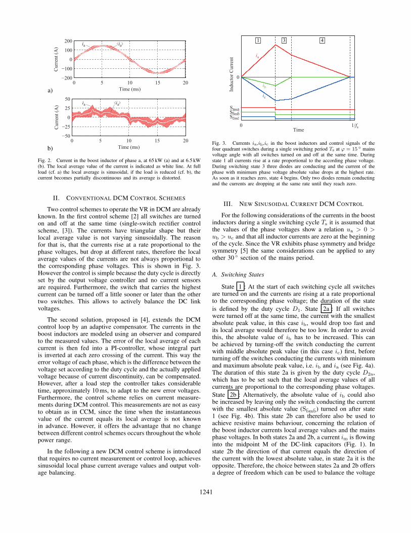
Two control schemes to operate the VR in DCM are alreadyknown. In the first control scheme [2] all switches are turnedon and off at the same time (single-switch rectifier controlscheme, [3]). The currents have triangular shape but theirlocal average value is not varying sinusoidally. The reasonfor that is, that the currents rise at a rate proportional to thephase voltages, but drop at different rates, therefore the localaverage values of the currents are not always proportional tothe corresponding phase voltages. This is shown in Fig. 3.However the control is simple because the duty cycle is directlyset by the output voltage controller and no current sensorsare required. Furthermore, the switch that carries the highestcurrent can be turned off a little sooner or later than the othertwo switches. This allows to actively balance the DC linkvoltages.
The second solution, proposed in [4], extends the DCMcontrol loop by an adaptive compensator. The currents in theboost inductors are modeled using an observer and comparedto the measured values. The error of the local average of eachcurrent is then fed into a PI-controller, whose integral partis inverted at each zero crossing of the current. This way theerror voltage of each phase, which is the difference between thevoltage set according to the duty cycle and the actually appliedvoltage because of current discontinuity, can be compensated.However, after a load step the controller takes considerabletime, approximately 10 ms, to adapt to the new error voltages.Furthermore, the control scheme relies on current measure-ments during DCM control. This measurements are not as easyto obtain as in CCM, since the time when the instantaneousvalue of the current equals its local average is not knownin advance. However, it offers the advantage that no changebetween different control schemes occurs throughout the wholepower range.
In the following a new DCM control scheme is introducedthat requires no current measurement or control loop, achievessinusoidal local phase current average values and output volt-age balancing.
0 1/fs
0
Time
Ind
uct
or
Cu
rren
t
1 3 4
ia
ib
ic
SamaSbmbScmc
Fig. 3. Currents ia,ib,ic in the boost inductors and control signals of thefour quadrant switches during a single switching period Ts at ϕ = 15 mainsvoltage angle with all switches turned on and off at the same time. Duringstate 1 all currents rise at a rate proportional to the according phase voltage.During switching state 3 three diodes are conducting and the current of thephase with minimum phase voltage absolute value drops at the highest rate.As soon as it reaches zero, state 4 begins. Only two diodes remain conductingand the currents are dropping at the same rate until they reach zero.
III. NEW SINUSOIDAL CURRENT DCM CONTROL
For the following considerations of the currents in the boostinductors during a single switching cycle Ts it is assumed thatthe values of the phase voltages show a relation ua > 0 >ub > uc and that all inductor currents are zero at the beginningof the cycle. Since the VR exhibits phase symmetry and bridgesymmetry [5] the same considerations can be applied to anyother 30 section of the mains period.
A. Switching States
State 1 : At the start of each switching cycle all switchesare turned on and the currents are rising at a rate proportionalto the corresponding phase voltage; the duration of the stateis defined by the duty cycle D1. State 2a : If all switcheswere turned off at the same time, the current with the smallestabsolute peak value, in this case ib, would drop too fast andits local average would therefore be too low. In order to avoidthis, the absolute value of ib has to be increased. This canbe achieved by turning-off the switch conducting the currentwith middle absolute peak value (in this case ic) first, beforeturning off the switches conducting the currents with minimumand maximum absolute peak value, i.e. ib and ia (see Fig. 4a).The duration of this state 2a is given by the duty cycle D2a,which has to be set such that the local average values of allcurrents are proportional to the corresponding phase voltages.State 2b : Alternatively, the absolute value of ib could alsobe increased by leaving only the switch conducting the currentwith the smallest absolute value (Sbmb) turned on after state1 (see Fig. 4b). This state 2b can therefore also be used toachieve resistive mains behaviour, concerning the relation ofthe boost inductor currents local average values and the mainsphase voltages. In both states 2a and 2b, a current im is flowinginto the midpoint M of the DC-link capacitors (Fig. 1). Instate 2b the direction of that current equals the direction ofthe current with the lowest absolute value, in state 2a it is theopposite. Therefore, the choice between states 2a and 2b offersa degree of freedom which can be used to balance the voltage
1241

a)0 1/fs
0
Time
Ind
uct
or
Cu
rren
t ia
ib
ic
SamaSbmbScmc
im
1 3 42a
b)
0 1/fs
0
Time
Ind
uct
or
Cu
rren
t ia
ib
ic
SamaSbmbScmc
1 3 42b
im
Fig. 4. Currents ia, ib, ic in the boost inductors, current into the DC-linkmidpoint im, and control signals of the four quadrant switches during a singleswitching cycle Ts using state 2a (a) and 2b (b) to achieve resistive behaviour.
sharing between the upper and lower DC-link capacitor. Theduration of state 2b is given by the duty cycle D2b which hasto be selected such that the local average values of the boostinductor currents are proportional to the corresponding phasevoltage. State 3 : After state 2a or 2b is finished all currentsare flowing through the free-wheeling diodes. The duration ofstate 3 is defined by the time the current ib takes to reach zero.State 4 : During state 4 only two diodes remain conducting,the duration of the state is given by the time it takes untilthe currents reach zero. After state 4 the currents remain zerountil the next switching period begins again with state 1. Theswitching cycles are repeated at a constant frequency fs as inCCM.
B. Calculation of the Duty-Cycles
The described five switching states, their equivalent cir-cuits, the current changes ∆ikn in each phase k in each staten and the duration Tn of each state are given in Tab. I. Usingthese equations the local average values of the currents in theboost inductors are calculated as
⟨ik⟩ =1
2(∆ik1T1 + (∆ik1 +∆ik2x)T2x + (∆ik1 +∆ik2x
+∆ik3)T3 + (∆ik1 +∆ik2x +∆ik3 +∆ik4)T4) fs(1)
with x being either a or b. In order to obtain sinusoidal inputcurrents the rectifier has to act like a symmetric three-phaseresistive load concerning the local current average values ⟨ik⟩.
Therefore, it is required that for each phase k the resistancerk = uk
⟨ik⟩ is the same, i.e. rk = r. Assuming!
k uk = 0 and!
k ik = 0, this condition is guaranteed if the resistance oftwo phases is the same. Therefore, solving the equation
ua
⟨ia⟩=
ub
⟨ib⟩(2)
with the local average values of the currents inserted from (1),yields the value of D2a or D2b that is necessary for resistivebehaviour, i.e. sinusoidal input currents after filtering switchingfrequency components. The value of D1 follows by insertingthe values D2a or D2b obtained from (2) into any of theequations r = uk
⟨ik⟩ for a required resistance r at the mains side.Analytic expressions for the duty cycles have been obtainedfor both switching patterns a and b. Using the expressions
D0 =
"
fsL
r, (3)
mmax =2 ·max(|ua|, |ub|, |uc|)
Upn, (4)
mmin =2 ·min(|ua|, |ub|, |uc|)
Upn(5)
the duty cycles for a switching cycle of either pattern a or bcan be calculated using the equations in Tab. II. Using theseanalytical expressions is possible in a circuit simulation, butbecause of the complexity of the expressions for pattern a, arealization in hardware is only possible using look-up tables.For ideal mains voltages
ua = U cos(ϕ)
ub = U cos(ϕ+ 120)
uc = U cos(ϕ+ 240)
with the mains angle ϕ and U = M · Upn
2 with the modulationindex M , the values of the duty cycles are shown for thefirst 30 section of the mains period in Fig. 5. The patternis mirrored and repeated throughout all other 30 sections ofthe mains period. It is observed that the duty cycle functionsare continuous and that they are therefore well suited for animplementation if one uses look-up tables.
C. Limits of Operation
It has been shown that the proposed control scheme allowsthe operation of the VR in DCM, maintaining sinusoidalcurrents and output voltage balancing. In this section thelimiting values are investigated that define the applicationrange of the control scheme.
1) Maximum input voltage: If the rectifier is operatedin CCM, the maximum input voltage depends on the thirdharmonic modulation function which is used to maximize thelinear modulation range [6]. Ideally a maximum modulationindex of Mmax = 2√
3≈ 1.15 can be achieved. It is observed
that for high values of the modulation index, the duty cyclefunctions of Tab. II result in negative values. Numericalinvestigations show that all duty cycle values are valid formodulation indices up to Mmax ≈ 1.12.
1242

TABLE I. SWITCHING STATES OF THE PROPOSED SINUSOIDAL CURRENT DCM CONTROL SCHEME, ASSUMING ua > 0 > ub > uc .
Switching State Sama,Sbmb,Scmc Equivalent Circuit Changes of inductor currents Duration of state
1 1 - 1 - 1
iaua
ibub
icuc
∆ia1 = T1L
· ua
∆ib1 = T1
L· ub
∆ic1 = T1L
· uc
T1 = D1fs
2a 1 - 1 - 0
iaua
ibub
icuc
Upn2
∆ia2a = T2a
L· (ua −
Upn
6 )
∆ib2a = T2aL
· (ub −Upn
6 )
∆ic2a = T2a
L· (uc +
Upn
3 )
T2a = D2a
fs
2b 0 - 1 - 0
iaua
ibub
icuc
Upn2
Upn2
∆ia2b = T2bL
· (ua −Upn
2 )
∆ib2b = T2b
L· ub
∆ic2b = T2bL
· (uc +Upn
2 )
T2b = D2bfs
3 0 - 0 - 0
iaua
ibub
icuc
Upn
∆ia3 = T3L
· (ua −2Upn
3 )
∆ib3 = T3L
· (ub +Upn
3 )
∆ic3 = T3
L· (uc +
Upn
3 )
T3 = −L·(∆ib1+∆ib2x)
ub+Upn3
4 0 - 0 - 0
iaua
icuc
Upn
∆ia4 = T4
2L · (ua − uc − Upn)
∆ib4 = 0
∆ic4 = T32L · (uc − ua + Upn)
T4 = −2L·(∆ia1+∆ia2x+∆ia3)
ua−uc−Upn
TABLE II. DUTY-CYCLES FOR RESISTIVE BEHAVIOUR OF THE RECTIFIER IN DCM.
Pat
tern
a
D1a =D0·((9m2
min+6mmin+2)mmax−(6mmin+2)m2max−3m3
min−4m2min)
√y
D2a =D1a·(9m
2minmmax−2m2
min−6mminm2max+4mmaxmmin−3m3
min−√
x)
(3m3min
−9m2min
mmax+4m2min
+6mminm2max−6mmaxmmin+2m2
max−2mmax)
x = (2mmax − 2−mmin)mmin(3mmin − 2)(2mmax −mmin)(m2max −m2
min)
y = 3m5min + (24m2
max − 23mmax + 2)m3min + (20m2
max − 8mmax − 12m3max)m
2min+
(√
x− 4m3max + 6m2
max)mmin +mmax(√
x+ 2mmax − 2m2max) + (7− 15mmax)m
4min
Pat
tern
b
D1b = D0√
2− 2mmax +mmin
D2b = D0√
2− 3mmin −D1b
2) Minimum resistance Rmin: Since the rectifier is oper-ating at constant switching frequency, the total time T for allstates is limited to
T = T1 + T2x + T3 + T4 <1
fs. (6)
Since the slopes of the currents are defined by the voltages(and the inductance of the boost inductors), the peak value ofthe current and therefore the minimum resistance which can beemulated for the mains considering local phase current averagevalues is limited. The lowest resistance rmin is normalizedas rmin = rmin,p.u. · R0 using a base resistor R0 = fsL,determined by the switching frequency and the boost induc-tance. The dimensionless value rmin,p.u. is only depending onthe relative values of the phase voltages with maximum and
minimum absolute value. It can be calculated by solving (6).For a switching cycle the minimum relative resistance is
rmin,p.u.,b =4
2 +mmin − 2mmax(7)
with mmax, mmin as defined in (5) and (4). It is possible tofind an analytic expression for rmin,p.u.,a for pattern a usingsymbolic math software, however, the result is too complicatedto be shown here. Instead it shall be mentioned that numericalinvestigations reveal
rmin,p.u.,a < 1.1rmin,p.u.,b. (8)
1243

a)
00.20.40.6
0.8
1
1.2
1 4
Mains Angle (°)
Mo
du
lati
on
In
dex
M
d1a
0 10 20 300
0.2
0.4
0.6
0.8
11.12
010.
20.3
0.4
Mains Angle (°)
d2a
0 10 20 30
0.5
b)
0.40.6
0.8
1
1.2
1.4
Mains Angle (°)
Mod
ula
tio
n I
nd
ex M
d1b
0 10 20 300
0.2
0.4
0.6
0.8
11.12
0.2
0.4
0.6
1
Mains Angle (°)
d2b
0 10 20 30
Fig. 5. Relative duty cycles dk =DkD0
for resistive behaviour for a switchingcycle using switching state 2a (a) and for a switching cycle using switchingstate 2b (b).
Therefore the local minimum resistance which allows DCMwith both patterns a and b can be approximated as
rmin,p.u. ≈4.4
2 +mmin − 2mmax. (9)
However, one is usually only interested in the minimumresistance which is achievable with both patterns a and bthroughout the whole mains period at a certain modulationindex M . This value,
Rmin,p.u.(M) = maxϕ∈[0,30]
(rmin,p.u.,a(M,ϕ), rmin,p.u.,b(M,ϕ)),
(10)is shown in Fig. 6. The minimum resistance which is achiev-able in DCM marks the border for the phase current controllersto switch to DCM. To avoid that the controller constantlyswitches between CCM and DCM a hysteresis has to be imple-mented, so that DCM is only entered if the voltage controllerrequires a resistance of, e.q. 2Rmin,p.u., and CCM is onlyre-entered if the required resistance drops below Rmin,p.u..Using such a hysteresis for the selection of the current controlmode requires that the operating ranges for DCM and CCMare overlapping. That is actually the case since at the valueRp.u. = Rmin,p.u. the current ripple in DCM is approximatelytwice as high than it is in CCM. Therefore operation in CCMwith satisfactory input current quality is possible for emulatedmains resistance values up to 2Rmin,p.u..
3) Maximum global midpoint current Im,max: Throughoutthe mains period (globally), the VR is able to supply an averagecurrent Im into the midpoint of the output voltage. In CCM theamount of current that can be supplied is proportional to thephase current amplitude and reduces with increasing modula-tion index [7]. At a modulation index M = 1 approximately
0 0.2 0.4 0.6 0.8 1 1.121
10
100
Modulation Index M
Rm
in,p
.u.
(p.u
.)
Fig. 6. Minimum relative resistance that can be emulated for the mainsthroughout the whole mains period using the DCM patterns a or b.
0 0.2 0.4 0.6 0.8 1 1.120
0.05
0.1
0.15
Modulation Index MI m
,max
,p.u
. (p
.u.)
Fig. 7. Relative maximum midpoint current global average valueIm,max,p.u., which is the maximum midpoint current global average valuethat can be supplied into the midpoint of the DC-link relative to the phasecurrent fundamental RMS value.
45 % of the phase rms current amplitude can be supplied intothe midpoint. In DCM there is also current supplied to the mid-point during states 2a and 2b. The maximum positive midpointcurrent is generated if state 2a is always used while the phasevoltage with the smallest absolute value is negative and state2b is always used while the phase voltage with the smallestabsolute value is positive. The global (mains period related)average current Im,max which is then fed into the midpointduring one mains period is normalized with the RMS valueIp of the phase current fundamental as base. The resulting
maximum relative midpoint current Im,max,p.u. = Im,max
Ipis
shown in Fig. 7 as a function of the modulation index M . It isobserved that the maximum midpoint current for modulationindices in the range of M ∈ [0.6, 1.1] amounts to at least 10 %of the phase current rms value. This is substantially less thanthe value which is possible in CCM (cf. [7]), but more thanenough to cover asymmetric leakage currents and to recoverfrom transient unbalances.
D. Simulated Waveforms
The proposed control scheme is demonstrated using an ide-alized circuit simulation of the VR for a phase-to-phase RMSvoltage of Un = 400V, a DC-link voltage of Upn = 800V,a switching frequency of fs = 28 kHz, a boost inductanceof L = 50µH and a resistance emulated for the mains ofR = 40Ω, corresponding to an input power of Pn = 4 kW.The differential mode (DM) voltage of the rectifier phase a,
1244

0 5 10 15 20−600
−400
−200
0
200
400
600
Time (ms)
DM
Vo
ltag
e u
dm
,a
udm,a
<udm,a>
Fig. 8. Simulated DM phase voltage udm,a of a VR operating in DCM andits local average ⟨udm,a⟩.
udm,a = uam − ucm with ucm = uam+ubm+ucm
3 = −umn isshown in Fig. 8. It is observed that other than in CCM theDM voltage always becomes zero during a switching periodwhich causes higher DM noise (compare to CCM DM voltagewaveform as shown in [8]). However, the common mode(CM) voltage ucm (Fig. 9 is substantially reduced compared toCCM (compare [8]), and its local average is almost sinusoidal,with three times the mains frequency. The total power ofthe switching frequency harmonics is therefore partitioneddifferently into CM and DM parts than in CCM operation.The simulated current waveform in the boost inductor ofphase a is shown in Fig. 10, indicating clearly a sinusoidallocal average value. In the simulation the output voltagesare balanced using bang-bang control, i.e. the control alwaysselects either pattern a or b depending on which one resultsin a midpoint current that compensates the voltage unbalancebetween the two output capacitors. If no midpoint current hasto be supplied to the output, the average of the midpoint currentover two switching cycles is almost zero as can be seen inFig. 11. The simulation shows that the calculated duty cycles infact allow sinusoidal currents in DCM, after filtering switchingfrequency components. However, the proposed scheme resultsin an increased DM component of the rectifier input voltages,but reduces the CM component. Using the two states 2a and 2balternatively depending on the sign of the voltage differencebetween the two output voltages, allows to reduce the lowfrequency component of the midpoint current virtually to zero.Since the values of the midpoint current of state 2a and state2b are not the same, the switching patterns a and b will be usedwith a ratio other than 1:1. However one could also use bothstates in one cycle (1-2a-2b-3-4); this way the average of themidpoint current during one switching period could be set tozero or to a defined value. An analytic solution for the requiredduty cycles in this case was not successful. Solving for theduty-cycles numerically would be possible, but would result ina look-up table for each duty cycle with the desired value ofmidpoint current as third dimension. However, since the DCMcontrol is only used for low power values, the magnitude ofthe midpoint current in DCM is not directly relevant for thedimensioning of the output capacitor.
E. Noise Emission
Contrary to the operation in CCM, all switches are turnedon at the same time if the proposed DCM control scheme is
0 5 10 15 20−150
−100
−50
0
50
100
150
Time (ms)
Co
mm
on
Mo
de
Vo
ltag
e u
cm ucm
<ucm>
Fig. 9. Simulated CM voltage ucm =uam+ubm+ucm
3 = −umn of aVR operating in DCM and its local average value ⟨ucm⟩ over two switchingcycles.
0 5 10 15 20−50
−25
0
25
50
Time (ms)
Induct
or
Curr
ent
ia
(A
) ia
<ia>
Fig. 10. Simulated current ia in the boost inductor of phase a of a VRoperating in DCM and its local average ⟨ia⟩.
used. Therefore higher differential mode (DM) noise emissionis expected. On the other hand lower common mode (CM)noise should be observed since the high frequency CM voltageamplitude in DCM is lower by approximately a factor of3 compared to CCM. For the design of the input filter thenoise as measured with an EMI test receiver is relevant.Therefore, for the comparision of the noise levels in CCMand DCM, the DM and CM noise parts of the simulatedrectifier input voltages are separately fed into a simulated [9]peak detection test receiver according to CISPR11 [10]. The
0 5 10 15 20−30
−20
−10
0
10
20
30
Time (ms)
Mid
poin
t C
urr
ent
im
(A
)
im
<im>
Fig. 11. Simulated midpoint current im of a VR operating in DCM and itslocal average value ⟨im⟩ over two switching cycles.
1245

a)
0.1 1 10
100
120
140
160
Frequency (MHz)
DM
PK
Vo
ltag
e (d
Bµ
V)
CCM
DCM
7.4dB
fs
b)
0.1 1 10
100
120
140
160
Frequency (MHz)
CM
PK
Vo
ltag
e (d
Bµ
V)
CCM
DCM
fs
9.1dB
Fig. 12. Simulated noise emission detected with a CISPR11 peak receiverfor the VR operating in CCM (blue) and in DCM (red). The DM noise withpeak (PK) detection is shown in (a). It is observed that the DM noise in DCMat switching frequency is higher than in CCM. However, the noise levels athigher frequencies in DCM are the same or a little lower than in CCM. TheCM noise with PK detection is shown in (b). It is shown that the CM noiselevel in DCM is lower than in CCM at all frequencies.
switching frequency of the simulated circuit is set to 200 kHz,so that the full PWM spectrum is shown by the CISPR detector.The resistance that the rectifier applies to the mains is set to thelowest value (Rmin) which represents the case of highest noiseemission. Both switching patterns a and b are used to balancethe output voltage using bang-bang control. The resulting noisespectra are shown in Fig. 12. It is confirmed that in DCMthe DM noise is 7.4 dB higher at switching frequency than inCCM. At higher frequencies the DM noise levels in DCM andCCM are comparable. On the other hand, the CM noise level inDCM is lower by 9.1 dB at all frequencies compared to CCM.Therefore, if the switching frequency is less than 150 kHz,which is the lowest frequency for which CISPR defines noiseemission limits, one can operate the rectifier in DCM usingthe same EMI filter as designed for CCM. If this is not thecase, one has to increase the DM attenuation of the filter by≈ 7.4 dB or increase the switching frequency in DCM toobtain higher filter attenuation.
IV. EXPERIMENTAL VERIFICATION
The simulated waveforms presented in Sec. III-D are gen-erated using a simplified circuit of the VR without EMI inputfilter, employing idealized switching devices and inductors.Furthermore, the duty cycles in the simulation are calculatedusing the exact expressions given in Tab. II. In order to showthat the proposed control scheme also works on real convertersystems the DCM control scheme has been implemented on a
0 5 10 15 20−600
−400
−200
0
200
400
600
Time (ms)
Vo
ltag
e u
am (V
)
uam
<uam>
Fig. 13. Measured bridge-leg voltage uam of the VR and its local averagevalue ⟨uam⟩.
0 5 10 15 20−50
−25
0
25
50
Time (ms)
Induct
or
Curr
ent
i a (A
)
ia
<ia>
Fig. 14. Measured current ia in the VR boost inductor of phase a and its localaverage value ⟨ia⟩. Small negative current values are caused by the reverserecovery of the free-wheeling diodes.
65 kW VR prototype operating at 28 kHz switching frequency.The system is shown in Fig. 16. The boost inductors of theprototype use amorphous cut-cores with air gaps, thereforegood linearity of the inductance is expected. The measurementsare performed with 800 V DC-link voltage at a three-phasemains voltage of 400 V phase-to-phase RMS with a load of4300 W at the DC-link. The voltage from rectifier input to theoutput midpoint M uam is shown in Fig. 13. Its local averagereveals the third harmonic component of the midpoint voltage.The measured current in the boost inductor of phase a is shownin Fig. 14. If current components above 9 kHz are removed, theTHD of the current in the boost inductor is 0.8 %. The THDof the rectifier input current, shown in Fig. 15, is improvedby the EMI filter to 0.3 %. The control is implemented on aTI TMS320F28335 floating point DSP using look-up tables.Four tables are used that contain the values of the relative duty-cycles d1a = D1a
D0, d2a = D2a
D0, d1b = D1b
D0, and d2b = D2b
D0.
The tables have 7 rows for mmin = 0..0.1..0.6 and 12 columnsfor mmax = 0..0.1..1.1. The relative duty cycles are storedwith a precision of 8 bits. In total the look-up tables thereforeadd up to only 337 Bytes. However, in order to be able toreach the stated values of THD, bilinear interpolation has to
be applied. The normalization base D0 =#
fsLr is calculated
directly on the DSP, although another 1D look-up table forapplicable values of
√r could also be used.
1246

0 5 10 15 20−15
−10
−5
0
5
10
15
Time (ms)
Mai
ns
Cu
rren
t i a
n (
A)
−450
−300
−150
0
150
300
450
Mai
ns
Vo
ltag
e u
an (
V)uanian
Fig. 15. Measured current ian of the VR (at the mains side of the EMI inputfilter) and the mains phase voltage uan. Because of the low power level, theEMI input filter causes a relatively high capacitive phase shift between currentand mains phase voltage. (A total of 50µ F filter capacity per phase causes acapacitive RMS phase current of 3.6 A. At full load the phase-shift betweenphase voltage and current is therefore less than ≈ 2 , at low power levelsthe phase shift increases.)
Fig. 16. 65 kW/28 kHz VR prototype used for the measurements to verify theproposed DCM control scheme. width × length × height = 33.6 cm × 37.4 cm× 5.4 cm (13.2 in × 14.7 in × 2.13 in), power density ϱ = 9.56 kW/dm3
(157W/in3)
V. CONCLUSION
A new way to control the Vienna Rectifier with discontin-uous phase currents has been proposed. The control requiresno current sensing, offers output voltage balancing and - otherthan simpler DCM control concepts - sinusoidal currents, afterfiltering switching frequency components. If the noise level atswitching frequency is not limited, which is usually the casefor switching frequencies fs < 150 kHz, the scheme can beused with an EMI input filter that was designed for CCMoperation. Although the functions to calculate the duty-cyclescan be expressed analytically, one would rather implementthem in hardware using look-up tables. Measurements on aprototype have shown that a THD of the input current of0.3 % is possible using 337 Bytes of look-up tables and bilinearinterpolation.
REFERENCES
[1] J. Kolar and F. C. Zach, “A novel three-phase utility interface minimiz-ing line current harmonics of high-power telecommunications rectifiermodules,” in Proc. of 16th Intern. IEEE Telecommunications EnergyConference (INTELEC), 1994, pp. 367–374.
[2] P. Ide, N. Froehleke, H. Grotstollen, W. Korb, and B. Margaritis, “Anal-ysis of three-phase/three-level rectifiers at low load and discontinuous
conduction mode,” in Proc. of 15th IEEE Applied Power ElectronicsConference (APEC), vol. 1, 2000, pp. 197–204.
[3] J. Kolar, H. Ertl, and F. C. Zach, “Space vector-based analyticalanalysis of the input current distortion of a three-phase discontinuous-mode boost rectifier system,” in Proc. of 24th IEEE Power ElectronicsSpecialists Conference (PESC), 1993, pp. 696–703.
[4] P. Ide, F. Schafmeister, N. Frohleke, and H. Grotstollen, “Enhancedcontrol scheme for three-phase three-level rectifiers at partial load,”IEEE Transactions on Industrial Electronics, vol. 52, no. 3, pp. 719–726, 2005.
[5] J. Kolar and T. Friedli, “The essence of three-phase pfc rectifier systems- part i,” IEEE Transactions on Power Electronics, vol. 28, no. 1, pp.176–198, Jan 2013.
[6] M. Hartmann, “Ultra-compact and ultra-efficient three-phase pwm recti-fier systems for more electric aircraft,” Ph.D. dissertation, ETH Zurich,Power Electronic Systems Laboratory, 2011.
[7] J. Kolar, U. Drofenik, and F. C. Zach, “Current handling capabilityof the neutral point of a three-phase/switch/level boost-type pwm(vienna) rectifier,” in Proc. of 27th IEEE Power Electronics SpecialistsConference (PESC), 1996, pp. 1329–1336.
[8] M. Hartmann, H. Ertl, and J. Kolar, “Emi filter design for high switchingfrequency three-phase/level pwm rectifier systems,” in Proc. of 25thIEEE Applied Power Electronics Conference (APEC), 2010, pp. 986–993.
[9] M. L. Heldwein, “EMC filtering of three-phase pwm converters,” Ph.D.dissertation, ETH Zurich, Power Electronic Systems Laboratory, 2007.
[10] Internationl Special Committee on Radio Interference - C.I.S.P.R.,Geneva, Switzerland, “Specification for industrial, scientific and med-ical (ism) radio-frequency equipment - electromagnetic disturbancecharacteristics - limits and methods of measurement - publication 11,”2004.
1247