news from the eipc eipc summer conference, berlin - june...
TRANSCRIPT

1
EIPC SPEeDNEWS The Weekly On-Line Newsletter from the European Institute of Printed
Circuits.
Issue 16 – July 2015
NEWS FROM THE EIPC
EIPC Summer Conference, Berlin - June 2015. Day 1 Berlin, capital of Germany and a world city of culture, politics, media and science, was venue for the 2015 EIPC Summer Conference, which attracted delegates from sixteen countries, including Russia, Hong Kong, Japan, Israel, USA and Canada as well as the European Union, to experience a programme of twenty-one technical presentations over two days, and a visit to the Berlin laboratories of Fraunhofer Institute, Europe’s largest application-oriented research organisation. EIPC Chairman Alun Morgan extended a warm welcome to delegates but was sad to report the passing of Brian Haken, whose name had been synonymous with the foundation and direction of UK and European printed circuit trade associations for many years. Alun followed his opening remarks with a keynote market overview and business outlook for the global electronics industry, presented on behalf of industry analyst and EIPC board member Walt Custer. Walt, noted for the alacrity of delivery of his statistics and trend lines, has a worthy deputy in Morgan. A mesmerising blur of information of the highest calibre, delivered at Custer-pace-plus!
2
Global and Eurozone purchasing managers’ indices remained marginally on the side of growth and world electronic equipment revenues were showing year-on-year revenue growth of about 1.7%, with a similar trend in Europe. Of a world PCB sales total of $60 billion, Europe represented about 4% and North America 5%. With acknowledgement to Michael Gasch for source material, Morgan reported that the European PCB industry had an acceptable year in 2014 though with only about 0.7% growth, and this was counter-balanced by losses due to the closure of some manufacturers, and stagnation in overall volume was seen as a consequence of ongoing transfer of high volume business to Asia. A group of five countries: Austria, Switzerland, Germany, France and UK, accounted for almost 80% of total European production volume. The automotive industry was sourcing only innovative products in Europe, more than 90% of its needs coming from outside Europe, and the increasing share of electronics per vehicle did not result in higher revenues for the PCB industry. In fact, there had been a net decline since 2010. The European production value of the highly competitive consumer, communication and computer industry market sectors had dropped by more than a third since 2010 and supplies of PCBs for industrial electronics had declined year-on-year by 1.4%. The UK and France remained very active in supplying the defence, aeronautic and space industries which had achieved strong growth in sales. The total number of manufacturers declined again in 2014, and in most cases the companies going out of business had been small, whilst others had joined larger groups to secure their survival. The manufacture of standard technology PCBs was falling at a slower rate than expected, and HDI, flex and flex-rigid had shown substantial growth. Custer’s World PCB model forecast 2.5% growth for the current year, and leading indicators suggested 1% growth in Europe.

3
Having concluded the market overview, Alun called forward EIPC board member Oldrich Simek of Pragoboard in Czech Republic and presented him with a plaque acknowledging his enormous contribution over many years and bestowing upon him Honorary Fellowship of the Institute.
New Technology was the theme for the first technical session, which began with a presentation from Sven Lamprecht, Director for Technology and Market Assessment in the Electronics Division of
Atotech Deutschland, entitled “Smart manufacturing systems pave the way for embedded technologies.” He considered the implications of the “More Moore” and “More than Moore” extensions of Moore’s Law in terms of the challenges they presented in the manufacture of package substrates. Over the coming five years, microvia diameters were forecast to trend to 20 microns, solder resist openings to 30 microns, and lines and spaces to
3 microns. Two major issues were the warpage and modulus of organic-based substrate materials, and glass was seen as a potential solution. Two major research groups were working on glass-based developments, Georgia-Tech Package Research Centre and Fraunhofer-Corning, and the first glass-core demonstrators had been produced, although there were still concerns about the effects of thickness and height variation on yield. “PowerPoint Engineering” did not accurately reflect the realities of surface topography on manufacturing yields. An alternative manufacturing proposition was to embed conductor features into the substrate, by direct laser structuring and panel plating without photoresist. The Laser-Embedded-Conductor Substrate had already been demonstrated. Lamprecht considered that many solutions to tomorrow’s challenges could be entirely new and disruptive, rather than modifications to existing methods.
4
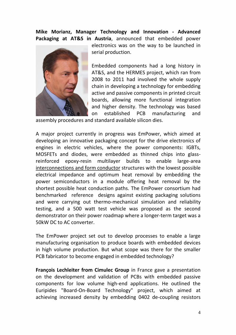
Mike Morianz, Manager Technology and Innovation - Advanced Packaging at AT&S in Austria, announced that embedded power
electronics was on the way to be launched in serial production. Embedded components had a long history in AT&S, and the HERMES project, which ran from 2008 to 2011 had involved the whole supply chain in developing a technology for embedding active and passive components in printed circuit boards, allowing more functional integration and higher density. The technology was based on established PCB manufacturing and
assembly procedures and standard available silicon dies. A major project currently in progress was EmPower, which aimed at developing an innovative packaging concept for the drive electronics of engines in electric vehicles, where the power components: IGBTs, MOSFETs and diodes, were embedded as thinned chips into glass-reinforced epoxy-resin multilayer builds to enable large-area interconnections and form conductor structures with the lowest possible electrical impedance and optimum heat removal by embedding the power semiconductors in a module offering heat removal by the shortest possible heat conduction paths. The EmPower consortium had benchmarked reference designs against existing packaging solutions and were carrying out thermo-mechanical simulation and reliability testing, and a 500 watt test vehicle was proposed as the second demonstrator on their power roadmap where a longer-term target was a 50kW DC to AC converter. The EmPower project set out to develop processes to enable a large manufacturing organisation to produce boards with embedded devices in high volume production. But what scope was there for the smaller PCB fabricator to become engaged in embedded technology? François Lechleiter from Cimulec Group in France gave a presentation on the development and validation of PCBs with embedded passive components for low volume high-end applications. He outlined the Euripides "Board-On-Board Technology" project, which aimed at achieving increased density by embedding 0402 de-coupling resistors

5
and capacitors in high Tg glass-epoxy substrates using the capabilities of a small PCB fabrication shop. Reliability was required to be to the long-term, harsh-environment standards demanded by civil avionics and telecommunications applications, and repairability was a further requirement. There were nine partners in the project, with a strong interaction between PCB fabricators, OEMs and EMS companies. The focus of this work package was the development of the PCB core containing the embedded passives. First step was to place the components on a carrier substrate, then create the core with this carrier and components, and build a rigid multilayer structure on it, resulting in a 10 layer multilayer with embedded 0402 components sandwiched between layers 5 and 6. Co-development between manufacturer and OEM had enabled robust design-for-manufacture rules to be established. Standard off-the-shelf passive chips with copper terminations were used, and interconnections between chips and copper tracks were made by laser drilling and copper plating. This basic structure gave the opportunity to optimise most of the critical procedures involved in the embedding operation, particularly in the complete filling around the components with resin, without voids or cracks. Initial reliability assessments on test vehicles had given good results, and long term tests were ongoing. The project was currently at the stage of final demonstrator manufacture, most of technical development work had been completed and here was an optimistic expectation that the embedding technology would fulfil the OEM requirements.
Whenever new technologies are developed, standardisation is needed to support development and industrial progress. Walter Huck, General Manager Quality and Environment at Murata Electronics Europe gave an update with reference to IEC and made a convincing argument for involving standards organisations at the earliest stage of the project. He commented that

6
international standards bodies, national bodies, consortia and private bodies coexisted but rarely cooperated, and that standardisation organisations were not really integrated. When innovation involved the development of complex new system technologies, embedding technology being a prime example, long-term cooperation of the various industries, standardisation bodies and interest groups was required, along the whole value chain and aligned with technology roadmaps. And a strategic approach was necessary if the innovation was to become a market success, with standardisation as one of the priorities. He described the approach taken by the IEC TC 91 Assembly Technology committee, and the standardisation strategy adopted by JISSO, from technology roadmap, through standardisation roadmap and publication plan, to the work programmes of the cooperating committees, resulting in the IEC 62878 Device Embedded Substrate series, four parts of which were already published, two were at draft stage, and a new generic specification was in preparation. But what of embedding for high power applications? No safety standards were yet in existence, and it could take several years to generate them. “If you want the technology available to the mass market in 2020, you’ve got to start developing standards and test methods now!” The theme for the second technical session was the status of inkjet in
PCB fabrication, with presentations from three industry experts and Pete Starkey as Moderator. Being cost-effective with imaging technology was the subject of the presentation by Gregory Stoeckli, Managing Director of First EIE in Switzerland. “What do European PCB shops look for when investing in manufacturing equipment?” he asked, and with amusing but meaningful illustrations, he demonstrated how perception, awareness and intuitive

7
understanding varied depending on people’s positions and points of view, those of the managing director and the production manager being typically contrasting examples. He clarified the difference between efficient and effective, stressed the importance of flexibility, and observed that the most effective solution need not be the most expensive. In the case of PCB fabrication, the typical SME was looking to produce complex PCBs as quickly and cost-effectively as possible, and was always eager to increase his margin without raising his price, by working more effectively and flexibly and maximising his yield. First EIE’s background was in film imaging and they had been in the business of developing and supplying photoplotters for over three decades. They had produced their first inkjet legend printer in 2002 and were now in their third generation of drop-on-demand equipment. Their emphasis was on flexibility, simplicity in operation and low-cost maintenance, and at 80% duty cycle their equipment could print 60 panels per hour at 600 dpi resolution with on-the-fly UV curing and a power consumption of only 400 watts. “Don’t believe all you read on data sheets!” was Stoeckli’s advice when making equipment choices.
Dr Boaz Nitzan, VP of Functional Inkjet Technology at Camtek in Israel, gave a detailed description of the recently introduced Gryphon SL, described as a full digital manufacturing station for PCB solder mask and legend by ink-jet technology. The equipment represented the latest innovation in Camtek’s 3D functional inkjet system and offered a “one-stop-shop” for solder mask and legend deposition by 3D inkjet technology, replacing both the traditional solder mask and the legend application
and imaging processes in PCB manufacturing. It was designed to enhance production by improving accuracy, reliability and yield, whilst reducing manpower demand and eliminating the need to treat waste products from the process.

8
The system used real-time alignment and built-in AOI to match the image to the actual panel, and the print-head recognised and followed the 3D topography of the PCB surface. The ink was immediately tack-dried with a built-in UV curing system. From a process point of view, the system had the advantages of reducing the number of stages from seven to three and the capability to print solder mask and legend consecutively from a single alignment, with consequent reduction in process cycle time. It occupied very little floor space and required only a single operator. Technical benefits included the ability to achieve zero clearance, to print different thicknesses in different areas, and to print gloss, semi-matt or matt from the same ink. Total cost savings of almost 50% per panel could be achieved compared with photoimaging processes. Don Monn, European Sales and New Product Development Manager for Taiyo America, took the published theme of the conference: “Improve profitability through technical leadership and innovation to meet future market requirements”, as the basis for a thought-provoking debate on the question: “Inkjet soldermask. Is it right for you?” delivered in his distinctive animated style, with the underlying message of getting things right first time. He went to great lengths to determine the real costs of rework and scrap - going far beyond those immediately visible, then analysed to the same level of detail the actual costs of the photoimageable solder mask process in a typical high-mix PCB fabrication shop manufacturing 3,500 panels per month, 50% screen-coated, 50% spray-coated. Not just the prime costs of materials and tooling, operator costs and equipment running costs but all of the peripheral consumables, down to squeegee rubber and sticky tape - amazing how all of these seemingly trivial costs added up to a substantial total! Returning to the key-word in the conference theme, he remarked: “Profitability is not a dirty word where I come from!” and reiterated the “Do it once, do it right” message, as a preface to the fast-approaching point in time when technology, in the shape of production-proven ink-

9
jet equipment and end-user qualified inks, would help the industry increase its profit margins. This session provoked more interactive dialogue than any other in the conference programme. Dr Nitzan in particular was inundated with requests for additional information and explanation on equipment capability and material performance, and delegates would have missed a substantial proportion of their lunchtime break if Pete Starkey had not reluctantly brought the discussion to a close. The theme of the afternoon session was the evaluation of new materials, processes, packaging and PCBs for the next generation of electronics “Made in Europe”, and was focused on the work of the Fraunhofer Institute for Reliability and Microintegration IZM in Berlin, with three technical presentations, moderated by Fraunhofer’s Dr Michael Töpper, followed by a visit to the Fraunhofer IZM laboratories in Berlin Mitte. Dr Ivan Ndip, Head of the Department of RF & Smart Sensor Systems, examined the demands on the PCB for future RF applications, with particular reference to the role of RF systems in the Internet of Things. IoT had a layered architecture: a device layer with RFID and RF sensor systems, a network layer of high-speed optical communication systems, a service and applications support layer with cloud computing systems for Big Data, and an applications layer, with RF wireless communication systems. System-integration technologies were the fundamental building blocks of RF systems, and for future RF applications the PCB could be considered either a key enabler or a bottleneck, it needed to ensure signal and power integrity whilst minimising electromagnetic interference. Critical material parameters were surface roughness and surface finish of the metallisation, and homogeneous permittivity, low moisture absorption, wide frequency range stable over a wide temperature range and low loss tangent of the dielectric. Fraunhofer had developed a holistic and systematic approach to testing and evaluating PCB materials, in cooperation with manufacturers like

10
Isola and Corning, and were now able to predict the issues at PCB level that could compromise RF performance, through 3D full-wave simulation, layout, fabrication, test structure design and RF measurement. Dr Ndip discussed the RF design of interconnects in multilayer PCBs, gave examples of RPD problems and how new design measures could optimise the electromagnetic performance of vias without using decoupling capacitors. He then considered the design, simulation and measurement of integrated antennas, showed the correlation between simulated and measured values, and demonstrated how a 77GHz antenna could be completely de-tuned as a consequence of typical PCB manufacturing tolerances. Lars Böttcher, Project Manager Embedded Die Technologies at Fraunhofer IZM gave a fascinating insight into next-generation PCB and panel-based packages using embedding technologies. He explained that cost reduction in semiconductor packaging could be achieved by an increase in production format size, and PCB embedding technology offered a potential solution, although for next-generation panel-level packaging, advanced processes and materials would be needed, together with improvements in resolution and accuracy. Warpage remained a major challenge, and polymer materials with controlled CTE and modulus, together with low shrinkage, were required, with designs optimised in terms of layer sequence and build-up. However, the production of embedded packages was ramping up rapidly. Already established in power and logic applications, growth would be seen in the smart-phone and computer markets, and embedding technology would soon be implemented at PCB manufacturers, semiconductor manufacturers and outsourced assembly and test (OSAT) companies. Fraunhofer IZM had already established a complete PCB manufacture and assembly line for substrate integration on 24” x 18” panels, and Böttcher described process sequences for embedding bare chips, packaged components and passive components using solder or adhesive

11
interconnects or alternatively direct copper interconnects, with examples of applications in modular systems. Böttcher discussed Fraunhofer’s collaboration in the EmPower Project which had been referenced in the earlier presentation of Mike Morianz from AT&S. The project aimed to industrialise double-sided copper plating on wafer level as a route to industrialising next-generation automotive power modules, and to combine high performance with small form factor. The process concept was based on epoxy coated foil or prepreg and copper foil with direct microvia connection from top and bottom side, which required double-sided copper metallization of the semiconductor. No soldering or sintering was used for die-attach, which was achieved by hot-bonding to B-stage epoxy resin. Power cores fabricated using this process were bonded to an IMS substrate with thermally conductive prepreg, and high-current connections were made by silver sintering. A 500-Watt demonstrator had been produced and it was forecast that power devices based on this technology would soon be in volume production.
Reliability and Environmental Aspects for Future PCB was the topic of Dr Olaf Wittler, Head of Environmental and Reliability Engineering at Fraunhofer IZM. He made it clear that environmental concerns would continue to be important technology drivers in the electronics industry. In the recent past, regulations such as the RoHS and ELV directives had resulted in increased performance demands on PCBs, and certain RoHS exemptions, originally permitted because
of a lack of appropriate substitute materials, were due to expire in the near future. New trends in use conditions, particularly in power and LED applications, continued to increase the temperature load on the PCB. Fraunhofer IZM had developed material characterisation techniques to determine copper properties and monitor dielectric degradation and were now able to measure yield stress of copper within via holes and non-destructively compare, test and qualify polymer dielectric materials

12
for long term and high temperature use. The reliability of solder joints at high temperatures was also an issue. New interconnect technologies were under development, capable of operating at high temperatures and showing higher reliability than standard interconnection methods. Environmental considerations such as the need to avoid climate change and save energy were driving the development of LED lighting and power electronics. There was a continuing trend towards improved resource efficiency and a consequent need for highly reliable electronics, and ongoing research at Fraunhofer IZM would determine how this trend would influence future electronics manufacturing. At the conclusion of the technical session, delegated had the opportunity of a refreshing 2km walk to Fraunhofer IZM (because the bus didn’t arrive!), and a privileged tour around the photonics laboratory, the power laboratory and the former flip-chip line, now converted to an embedding line. A long and interesting day concluded with a conference dinner in downtown Berlin.
EIPC Summer Conference, Berlin June 2015.
Day 2 Refreshed after an excellent conference dinner and, for most, a good night’s sleep, delegates returned for the second day of the EIPC Summer Conference in Berlin, continuing the theme of improving profitability through technical leadership and innovation to meet future market requirements, with sessions on materials and processes for high performance PCBs and advanced material testing strategies to meet OEM and ODM needs. The materials and processes session was moderated by Professor Martin Goosey, EIPC Vice President Technology, and his first speaker was Martyn Gaudion, MD of Polar Instruments with a presentation entitled “Fast and Fine: addressing the challenges of impedance measurement on fine line traces.” Beginning with his customary declaration that “All models are wrong, but some of them are useful”, and with reference to the differences between “lossless” and “lossy” transmission lines, he explained that fabricators

13
building designs for frequencies below 2GHz typically worked on the basis of lossless characteristic impedance Zo, whereas in designs of 2GHz and above the focus shifted towards measurement of insertion loss in the transmission line. There was a grey area where lines operating at moderate speeds experienced low frequency losses because of fine line geometries, and the correlation of measured impedance with modelled results was not as precise as would be expected. From a few MHz to 2GHz, losses were small enough to ignore, and impedance could appear the same at any point along the line. !00% of the signal energy was transmitted along the line and any losses were primarily the result of mismatch of input and output impedance causing reflections. From 2GHz upwards, losses in copper and dielectric absorbed power from the signal and, as frequency increased, proportionately less signal was transmitted. When attempting to make a measurement of the characteristic impedance of a fine line, these accumulated DC and AC resistances caused a slope on the TDR trace so that the observed value varied depending whereabouts on the trace it was measured. Launch Point Extrapolation was a method of computing the instantaneous or incident impedance by removing the DC and AC resistance effects, enabling better correlation between field solver modelled and actual measured values.
Dominique Garmy, from DuPont Circuit and Packaging Materials discussed flexible circuit materials for high temperature environments, commenting that although an increasing number of automotive, military, aerospace, oil and gas applications required flexible circuits capable of withstanding high service temperatures, there had been a shortage of suitable materials and a lack of good test methods for evaluating and qualifying them. Failure
mechanisms fell into three categories: adhesion loss, between copper and dielectric or between dielectric layers, embrittlement of dielectric and embrittlement of copper. In most cases flexible circuit dielectrics

14
were the first to fail, thermoset adhesives being more sensitive to embrittlement than polyimide films. One UL rating for high temperatures was based on relative thermal index (RTI), determined by loss of tensile strength and dielectric strength with long term thermal ageing. Samples were tested without copper so the test did not relate to any copper-adhesion loss and by itself was not a good measure of the capability of a copper clad laminate. The other UL test was maximum operating temperature (MOT), primarily determined by loss of copper adhesion after accelerated heat aging. The IPC service temperature test IPC-TM 2.6.21B appeared to work well for testing copper clad laminates but not as well for bondplies and coverlays. A new coverlay test, based on bend-testing, had been demonstrated, and overall results clearly indicated that all-polyimide clads, bondplies and coverlays provided the highest service temperature performance, with results close to industry experience. DuPont would continue to refine the new coverlay service temperature test and proposed to recommend its adoption by IPC.
Eric McLean, Sales Manager at Cambridge Nanotherm in the UK, discussed a nanoceramic dielectric designed to expand the performance of metal-in-board PCBs. Traditional metal-in-board substrates were limited in performance by the use of polymeric materials to provide electrical insulation and mechanical adhesion between the copper conductor layer and the aluminium core. These polymers had significant thermal resistance
and a low degradation temperature which tended to restrict their continuous operating temperature to below 150 °C. McLean described an innovative electrolytic process for converting the surface of aluminium to a dense, strongly adherent, layer of nanoceramic, the dielectric properties of which were better than those of sintered alumina, such that only a 10 micron layer was required for electrical insulation. “It’s alumina, but not as you know it!” Since the nanoceramic material had good thermal conductivity, the thermal resistance of the coating, quoted as 0.014 °C.cm2/W, was the lowest currently available. Direct metallisation of the nanoceramic

15
eliminated all organic constituents in the construction and enabled sustained operation at temperatures above 250 °C. Because the nanoceramic was formed by a self-levelling conversion process, through and blind vias could be straightforwardly coated, irrespective of aspect ratio, so that double-sided circuits could readily be fabricated. And the coating was capable of withstanding bending without cracking or peeling, so that substrates could be post-formed into three-dimensional shapes. Application examples included LED chip-on-board modules, LED light engines, power amplifiers and switching power supplies.
Hiroyoshi Tojima, from MEC Company in Japan, described how an anisotropic etching technology developed for chip-on-film applications was being adapted for HDI and packaging applications. In chip-on-film devices such as the drivers for LCD displays, 10 micron lines and spaces on 8 micron foil were typical and satisfactory definition was difficult to achieve by conventional subtractive techniques because of lateral
attack by the etchant. Semi-additive techniques gave better conductor cross-section but were comparatively complex and higher in process cost. Physical limitations were the non-planarity of plated conductors and a tendency for undercut at the flash-etching stage to initiate peeling-off of fine conductor features. So there was a technical demand for an anisotropic subtractive process, to which MEC Company had responded by developing an additive for cupric chloride based etchant, which formed a protective film at the sidewall and inhibited lateral etching, giving a remarkable improvement in etch factor. Although etching machine set-up was critical and there was a narrow operating window, the process had established almost 100% market share with Japanese and Korean chip-on-film manufacturers. So it was logical to develop a variant of the process for HDI and packaging manufacture, where the line width demands were not as crucial but panel sizes were much larger and double-sided etching was required. Another complication was that the copper was likely built up in layers of material of different origin, for example: foil copper, catalyst, electroless copper, electroplated copper, all of which could have different etching

16
characteristics. The target was to achieve an etch factor better than 4.0 on 40 micron lines and spaces in 18 micron copper. Extensive trials had been carried out over a wide range of operating parameters and circuit geometries, and it had been shown that the addition of only 5% of MEC’s proprietary additive in standard etching equipment achieved the target etch factor whilst reducing contact time by 10-15%
Hiroyoshi Tojima having demonstrated what could be achieved by state-of-the-art subtractive processing, Multiline International Europe MD and former EIPC chairman Paul Waldner came from the opposite direction to talk additive! Many had tried and failed in the quest for a process that would open up opportunities in full-additive circuit fabrication, and adhesion of metal to substrate had been a problem that had not been satisfactorily overcome. With the rapid emergence of PCB technologies based on ultra-thin
bendable and stretchable substrates, how could copper be made to stick reliably? Waldner presented a paper written by Alex Richardson, VP of Global Strategic Operations for eSurface, entitled: “A novel approach for applying metallization to ultra-thin substrates”, introducing an innovative photosensitive catalyst with the proprietary name of Covaler which, besides PCB manufacture, had a wide range of applications including decorative metallisation, wearable technology, semiconductor packaging, medical, military, automotive, solar, and other industrial uses. In PCB fabrication, eSurface’s Covaler had been specifically formulated for inner and outer circuit board layer constructions, flexible circuits and interposers. Claimed to be a breakthrough enabler, it was compatible with the majority of industry-standard base materials and opened up opportunities for many non-traditional materials. Applied as a surface treatment using a conventional wet process line, the Covaler bonded to the substrate surface and became autocatalytic to electroless copper upon exposure to UV light, so could be used directly to fabricate full-additive circuitry. Alternatively, it could be used

17
as the base for all-over electroless copper plating in a semi-additive process capable of very fine-line resolution. Alun Morgan returned to moderate the final conference session, this time in his role as Project Facilitator and European Representative for the High Density Packaging User Group, HDPUG. He introduced HDPUG as a non-profit trade organisation whose member companies were involved in the supply chain of producing products utilising high-density electronic packages. HDPUG was entirely member-driven, its members deciding what technical areas to pursue and what topics to investigate, in order to stay focused on the most important issues affecting the electronics manufacturing industry. Its stated mission was to reduce the costs and risks for the electronics industry by improving cooperation between system integrators, contract assembly manufacturers and suppliers in the high-density packaging development and design process, using member resources, supplemented by a small staff. HDPUG’s activities revolved around the spirit of cooperative R&D, where members could gain much more by sharing resources and expertise to address issues of common interest than by duplicating work in each member company. This enabled major problems and global technical issues to be resolved in a fraction of the time and at a fraction of the cost it would take for companies to do it individually. The group was focused on the characterisation and reliability of electronic assemblies and sub-assemblies. As technology progressed, new materials and new processes were being developed, and new requirements, for example environmental regulations, were influencing how electronic assemblies were built. It was in the interest of all parties that products built with these new materials and processes were reliable and cost effective, and HDPUG ran projects to evaluate and understand the effects of material and process change. 28 R&D projects had been completed in the last three years, and 27 were currently in progress. Morgan described the process by which projects were conceived, defined, approved and executed, using the Harsh Use Environment Alloy Evaluation project as an example, and then welcomed Marika Immonen from TTM Technologies to give an update on the second phase of the Optoelectronic project: “Optoelectronic Interconnect - preferred

18
solution for short-range interconnect?” This project, which involved a total of 31 contributing companies, had begun five years previously with the objective of evaluating the feasibility of optical waveguide based technologies on PCBs, determining performance benefits and limitations using polymer waveguides and fibres for 1-2 metre links. The focus was on optical fibre and waveguide link characteristics, practical connectivity options and end-to-end link implementations. The first phase, in which test vehicles with multiple waveguide components had been used to verify the practicality of using optical fibres for short-range interconnect, had been completed. The second phase was at the definition stage, and proposed to use the viable building blocks from Phase 1 to build a more complex system-level demonstrator with end-to-end optical links. Ms Immonen gave a comprehensive overview of the design rules and interconnection models for the OE2 demonstrator, which would have a combination of free-standing flexible waveguides, embedded glass wave guides and embedded polymer waveguides.
The final speaker of the day was Bill Birch from PWB Interconnect Solutions, and if there had been a prize for the longest title of the conference, he would have been a sure winner with “Quantifying and benchmarking new PWB materials reliability, electrical performance and thermal properties following exposure to today’s lead free assembly environment.” A long-term corporate member of HDPUG,
Birch had been engaged in an ongoing programme to evaluate material reliability. “Designers can get carried away and let electrical properties take precedence over reliability. We need a balance of electrical performance with reliability and manufacturability” Working with HDPUG to build up a database of PCB material properties, he had characterised 98 materials to date and there were 22 new materials currently being evaluated. Birch reviewed the results of Phase 3 of the

19
HDPUG Materials Reliability study, in which twelve materials - two high-Tg FR4, six halogen-free and four high-speed - were each constructed in two resin contents as a 20-layer test vehicle, 2.5 mm thick, with 0.25 mm drilled holes. For consistency, all had been fabricated simultaneously by the same manufacturer. The test vehicles were all subjected to six reflow cycles at 260°C, then tested using IST and DELAM procedures. All of the materials claimed to be lead-free compatible - not all were! 15 of 24 delaminated in the 0.8 mm grid area and 8 of 24 in the 1.0 mm grid area, whereas all had passed the old IPC solder-float test - dating from 1961 and clearly not representative of current assembly conditions. The delamination failures observed raised questions which needed to be answered by laminate manufacturers. They tended to be cohesive failures across the central zone of the construction, and compromised the critical glass-resin interface. The question of “what’s good enough?” to satisfy the customer’s needs would always be the determining factor, and quantifying the overall PTH via reliability performance in terms of a materials ranking proved difficult, because of the complicating effect of cohesive material damage. Alun Morgan brought the proceedings to a close. Another in a long series of highly successful and informative EIPC conferences, drawing the industry together with a well-selected programme of technical presentations of current relevance and interest, interwoven with an abundance of networking opportunities and a very positive community spirit.
Thanking all presenters for their contribution and delegates for their attention and support, he especially acknowledged EIPC Executive Director Kirsten Smit-Westenberg (r) and Event Manager Sonja Derhaag for their superbly professional organisation of the occasion.
~~
20
I am once again grateful to Alun Morgan for allowing me to use his photographs.
Pete Starkey I-Connect007 June 2015
EIPC is most grateful to Pete for allowing us to use his excellent review – Ed.

EIPC SPEeDNEWS The Weekly On-Line Newsletter from the European Institute of Printed Circuits.
Issue 16 – July 2015
NEWS FROM GERMANY
Seica SpA has appointed Marc Schmuck as the new Sales Manager for Seica Deutschland.
Before joining SEICA Marc held leading positions at well‐known electronics manufacturers, responsible for customer support and sales. He has considerable experience and knowledge in building and maintaining, valued customer relationships. Marc’s first priority is to continue this dedication to customer service in his new role at Seica Deutschland. “My goal is to enlarge our sales and support
team, and to raise the profile of SEICA high‐value products and software solutions for the German electronics manufacturing market,” he stated. Since his appointment on 01 May 2015, he has particularly focused on customer contact, customer fulfillment, quality, reliability and customer relations, as well as maintaining close co‐operation with SEICA’s sales partners. As well as consulting directly with customers, he will also support existing local sales partners. Marc and his team covering application, service and spare part procurement will support the sales regions of Germany, Austria and Switzerland from Seica’s Munich Demo and Support Center.

Seica offers its customers a complete line of in‐house developed test solutions. It has strong partnerships with companies in production and inspection, providing a large portfolio of automatic test systems and selective soldering systems across the entire production line. At a time when globalization is increasingly challenging local competitiveness, Seica has developed a sound sales strategy with a strong, local presence in Italy, France, Germany, USA and China. The company offers customers premium service and full support from a professional team of experts. Founded in 1986, Seica S.p.A. is a global manufacturer of automatic test systems and selective soldering systems. It supplies turnkey and custom installations for major companies in the telecommunications, automotive and IT to medical and avionics markets, as well a multitude of contract manufacturers’ parts. The company has an installed base of more than 1,700 systems, on four different continents. About Seica Seica S.p.A, founded 1986, is a global manufacturer of automatic test systems and Selective Solder equipment, with an installed base of more than 1700 systems, on four different continents. Seica offers its customers complete automated, Laser‐based Selective solder solutions, as well as a complete line of test solutions which includes bed of nail and Flying Probe testers; these have the ability to perform a manufacturing defect analysis, In‐Circuit tests, functional tests and optical tests on loaded boards, also on „Second and Third Level Electronic Modules“ and bare boards. Seica S.p.A Corporate headquarters in Italy, with offices in France, Germany, USA, and China and has a worldwide distributor network. www.seica.com

EIPC SPEeDNEWS The Weekly On-Line Newsletter from the European Institute of Printed Circuits.
Issue 16 – July 2015
NEWS FROM THE UK
Phil Crabb to Boost Business Development at Active‐PCB Solutions Contact Electronics Manufacturer and NPI specialist, Active‐PCB Solutions, has appointed Phil Crabb as Business Development Manager. He will work alongside Sales Manager Helen Montague, to increase sales and drive the company’s activities in the UK and overseas. Phil brings over a decade of experience in quality assurance and technical sales, with over eight years at Exception PCB and Exception EMS including international sales for UK, Europe, Israel and USA. His appointment will boost Active’s ability to support customers comprehensively from prototyping and NPI through to full production including high‐volume assembly. “Phil has an outstanding record in the manufacturing services business, and we are delighted to have his skills and energy on board,” said Active‐PCB spokesperson. “He will not only develop our core UK customer base, but will also connect with our overseas team to enhance service for customers with higher‐volume production needs.” “Active‐PCB enjoys a strong position, with facilities and expertise among the best in the industry,” commented Phil Crabb. “This is an exciting opportunity to help take the business forward by strengthening our relationships with current customers and establishing new links with leading UK OEMs.”

Hayling Island Autumn Seminar 2015
ICT Evening Seminar at the
Newtown House Hotel, Hayling Island 22nd September
The RE‐INDUSTRIALISATION of EUROPE Interim list of Papers
ROMANIA ‐ Joining the EU and the supply chain opportunities.
Repatriating PCB fabrication from Asia to Europe – ie Romania
Sculptured Circuits and SMI Surface Mount Interconnects
At the close of the seminar, a Romanian Quartet will be performing some classical music during the buffet
Registration from 1700 Seminar starts at 1730. Enquiries to Bill Wilkie [email protected]
Supported by SPIRIT CIRCUITS

EIPC SPEeDNEWS The Weekly On-Line Newsletter from the European Institute of Printed Circuits.
Issue 16 - July 2015
PRINTED ELECTRONICS NEWS
Robust new process forms 3D shapes from flat sheets of graphene Researchers from the University of Illinois at Urbana‐Champaign have developed a new approach for forming 3D shapes from flat, 2D sheets of graphene, paving the way for future integrated systems of graphene‐MEMS hybrid devices and flexible electronics. "To the best of our knowledge, this study is the first to demonstrate graphene integration to a variety of different microstructured geometries, including pyramids, pillars, domes, inverted pyramids, and the 3D integration of gold nanoparticles (AuNPs)/graphene hybrid structures," explained SungWoo Nam, an assistant professor of mechanical science and engineering at Illinois. "The flexibility and 3D nature of our structures will enable intimate biosensing devices which can be conformed to the shape and characteristics of human skin and other biological systems. The 3D protruding micro‐structures can also achieve enhanced sensitivity by maximizing the effective contact area between the sensors and non‐flat surfaces. We also expect that our new 3D integration approach will facilitate advanced classes of hybrid devices between microelectromechanical systems (MEMS) and 2D materials for sensing and actuation." Graphene, a two‐dimensional honeycomb lattice of sp2‐bonded carbon atoms, has been widely studied due to its high carrier mobility, chemical inertness, and biocompatibility. To date, various reported methods of graphene transfer have been mostly limited to planar or curvilinear

surfaces due to the challenges associated with fractures from local stress during transfer onto 3D microstructured surfaces. "Our method utilizes wet‐transfer and adaptive substrate‐engineering, providing several key advantages over other fabrication/integration methods of 3D graphene," stated Jonghyun Choi, a graduate student in Nam's research group and first author of the article, "Three‐Dimensional Integration of Graphene via Swelling, Shrinking, and Adaptation," appearing in Nano Letters. "Our results demonstrate a simple, versatile, and scalable method to integrate graphene with 3D geometries with various morphologies and dimensions. Not only are these 3D features larger than those reported in previous works, but we also demonstrate the uniformity and damage‐free nature of integrated graphene around the 3D features." The researchers' robust approach to integrate graphene onto 3D microstructured surfaces maintains the structural integrity of graphene, where the out‐of‐plane dimensions of the 3D features vary from 3.5 to 50 μm. The process incorporates three sequential steps: 1.) substrate swelling using a solvent that 2.) shrinks during the evaporation process, allowing graphene to 3.) adapt, or conform to the shape of a prepared substrate, to achieve damage‐free, large area integration of graphene on 3D microstructures. "Our swelling, shrinking, and adaptation steps are optimized to minimize the degree of graphene suspension around the 3D microstructures and facilitate successful 3D integration," Nam added. "We control the amount of substrate swelling by adjusting the time of immersion in organic solvent and the mixing ratios of monomer and curing agent of the polydimethylsiloxane (PDMS) substrate." Detailed scanning electron microscopy, atomic force microscopy, Raman spectroscopy, and electrical resistance measurement studies show that the amount of substrate swelling, as well as the flexural rigidities of the transfer film, affect the integration yield and quality of the integrated graphene. To demonstrate the versatility of their approach, the researchers applied the process to a variety of 3D microstructured geometries, as well as integrating hybrid structures of graphene decorated with gold nanoparticles onto 3D microstructure substrates, demonstrating the compatibility of the integration method with other hybrid nanomaterials. In addition to Nam and Choi, the article's co‐authors include Hoe Joon Kim, Michael Cai Wang, Juyoung Leem, and Professor William P. King,

from the Department of Mechanical Science and Engineering at Illinois. This work was supported by the Air Force Office of Scientific Research/Asian Office of Aerospace Research Development Nano Bio Info Technology (NBIT) Phase III Program, the American Chemical Society Petroleum Research Fund, the Korean‐American Scientists and Engineers Association and the National Science Foundation. Experiments were carried out in part in the Frederick Seitz Materials Research Laboratory and the Micro and Nano Technology Laboratory, and the Beckman Institute Imaging Technology Group at Illinois. Source: University of Illinois First flexible phase‐change random access memory Phase change random access memory (PRAM) is one of the strongest candidates for next‐generation non‐volatile memory for flexible and wearable electronics. In order to be used as a core memory for flexible devices, the most important issue is reducing high operating current. The effective solution is to decrease cell size in sub‐micron region as in commercialized conventional PRAM. However, the scaling to nano‐dimension on flexible substrates is extremely difficult due to soft nature and photolithographic limits on plastics, thus practical flexible PRAM has not been realized yet. Recently, a team led by Professors Keon Jae Lee and Yeon Sik Jung of the Department of Materials Science and Engineering at KAIST has developed the first flexible PRAM enabled by self‐assembled block copolymer (BCP) silica nanostructures with an ultralow current operation (below one quarter of conventional PRAM without BCP) on plastic substrates. BCP is the mixture of two different polymer materials, which can easily create self‐ordered arrays of sub‐20 nm features through simple spin‐coating and plasma treatments. BCP silica nanostructures successfully lowered the contact area by localizing the volume change of phase‐change materials and thus resulted in significant power reduction. Furthermore, the ultrathin silicon‐based diodes were integrated with phase‐change memories (PCM) to suppress the inter‐cell interference, which demonstrated random access capability for flexible and wearable electronics. Their work was published in the March issue of ACS Nano:

"Flexible One Diode‐One Phase Change Memory Array Enabled by Block Copolymer Self‐Assembly." Another way to achieve ultralow‐powered PRAM is to utilize self‐structured conductive filaments (CF) instead of the resistor‐type conventional heater. The self‐structured CF nanoheater originated from unipolar memristor can generate strong heat toward phase‐change materials due to high current density through the nanofilament. This ground‐breaking methodology shows that sub‐10 nm filament heater, without using expensive and non‐compatible nanolithography, achieved nanoscale switching volume of phase change materials, resulted in the PCM writing current of below 20 uA, the lowest value among top‐down PCM devices. This achievement was published in the June online issue of ACS Nano: "Self‐Structured Conductive Filament Nanoheater for Chalcogenide Phase Transition." In addition, due to self‐structured low‐power technology compatible to plastics, the research team has recently succeeded in fabricating a flexible PRAM on wearable substrates. Professor Lee said, "The demonstration of low power PRAM on plastics is one of the most important issues for next‐generation wearable and flexible non‐volatile memory. Our innovative and simple methodology represents the strong potential for commercializing flexible PRAM." In addition, he wrote a review paper regarding the nanotechnology‐based electronic devices in the June online issue of Advanced Materials entitled "Performance Enhancement of Electronic and Energy Devices via Block Copolymer Self‐Assembly." Source: KAIST

Issue 3 – July 2015 NEWS FROM IPC
North American PCB Results in May Were Mixed but Book‐to‐Bill Ratio Remains
Positive IPC Releases PCB Industry Results for May 2015
IPC have announced the May findings from its monthly North American Printed
Circuit Board (PCB) Statistical Program. Sales were down slightly but orders were
up. The book‐to‐bill ratio held steady at 1.02.
Total North American PCB shipments decreased 4.2 percent in May 2015
from May 2014, and year‐to‐date shipment growth declined to ‐1.8 percent.
Compared to the previous month, PCB shipments were down 3.5 percent.
PCB bookings increased by 10.4 percent compared to May 2014, returning
the year‐to‐date order growth rate to positive territory at 1.3 percent. Orders
increased 0.9 percent in May compared to the previous month.
“North American PCB sales continued below last year’s level, but orders
resumed positive growth and the book‐to‐bill ratio remains positive for the eighth
straight month,” said Sharon Starr, IPC’s director of market research. “This indicates
the likelihood of strengthening sales growth in the second half of this year,” she
added.
Detailed Data Available
The next edition of IPC’s North American PCB Market Report, containing
detailed May data from IPC’s PCB Statistical Program, will be available within the
next week. The monthly report presents detailed findings on rigid PCB and flexible
circuit sales and orders, including separate rigid and flex book‐to‐bill ratios, military

and medical market growth, demand for prototypes, and other timely data. This
report is available free to current participants in IPC’s PCB Statistical Program and
by subscription to others. More information about this report can be found
atwww.ipc.org/market‐research‐reports.
Interpreting the Data
The book‐to‐bill ratios are calculated by dividing the value of orders booked
over the past three months by the value of sales billed during the same period from
companies in IPC’s survey sample. A ratio of more than 1.00 suggests that current
demand is ahead of supply, which is a positive indicator for sales growth over the
next three to six months. A ratio of less than 1.00 indicates the reverse.
Year‐on‐year and year‐to‐date growth rates provide the most meaningful
view of industry growth. Month‐to‐month comparisons should be made with
caution as they reflect seasonal effects and short‐term volatility. Because bookings
tend to be more volatile than shipments, changes in the book‐to‐bill ratios from
month to month might not be significant unless a trend of more than three
consecutive months is apparent. It is also important to consider changes in both
bookings and shipments to understand what is driving changes in the book‐to‐bill
ratio.
IPC’s monthly PCB industry statistics are based on data provided by a
representative sample of both rigid PCB and flexible circuit manufacturers selling in
the USA and Canada. IPC publishes the PCB book‐to‐bill ratio at the end of each
month. Statistics for the current month are available in the last week of the
following month.
EIPC SPEeDNEWS The Weekly On-Line Newsletter from the European Institute of Printed Circuits.
INTERNATIONAL DIARY 2015 ‐2016
IPCA SHOW New Delhi, India 20th -22nd August 2015 www.ipcaindia.org SMART Group European Conference 2015 22nd – 23rd September 2015 NPL, Teddington www.smartgroup.org EIPC-EFRA-CEFIC Workshop 23rd September 2015 Cefic, Brussels www.eipc.org TPCA SHOW Taipei, Taiwan 21st -23rd October 2015 www.tpcashow.com EIPC @ PRODUCTRONICA Messe München, stand B1-529 10th – 13th November 2015 www.productronica.com HKPA SHOW Shenzen, China 2nd-4th December 2015 www.hkpca.org 2016 Southern Manufacturing 2016 FIVE, Farnborough, Hampshire, GU14 6XL, UK 9-11 February 2016 [email protected]