newsletter - sid, the society for information display · excimer laser annealing which has issues...
TRANSCRIPT
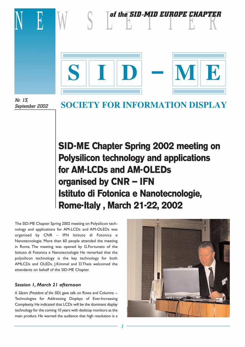
The SID-ME Chapter Spring 2002 meeting on Polysilicon tech-nology and applications for AM-LCDs and AM-OLEDs wasorganised by CNR – IFN Istituto di Fotonica eNanotecnologie. More than 60 people attended the meetingin Roma. The meeting was opened by G.Fortunato of theIstituto di Fotonica e Nanotecnologie He remarked that thepolysilicon technology is the key technology for bothAMLCDs and OLEDs. J.Kimmel and D.Theis welcomed theattendants on behalf of the SID-ME Chapter.
Session 1, March 21 afternoon
A. Silzars (President of the SID) gave talk on Rows and Columns --Technologies for Addressing Displays of Ever-IncreasingComplexity. He indicated that LCDs will be the dominant displaytechnology for the coming 10 years with desktop monitors as themain product. He warned the audience that high resolution is a
1
NEWSLETTERof the SID-MID EUROPE CHAPTER
S I D M ESOCIETY FOR INFORMATION DISPLAY
Nr. 13, September 2002
SID-ME Chapter Spring 2002 meeting onPolysilicon technology and applications for AM-LCDs and AM-OLEDsorganised by CNR – IFNIstituto di Fotonica e Nanotecnologie, Rome-Italy , March 21-22, 2002

cost driver and not to increase the resolution when not requiredby the application. He concluded that manufacturing costsbecome the major driving force for development.This requiressimpler (non-semiconductor) production processes. In the devel-opment of new materials a slow evolution is expected.P.Migliorato (Univ.of Cambridge) talked about the trap-assisted gen-eration-recombination processes and transient effects in poly-sil-icon TFTs.The generation -recombination processes are depen-dent on the nature and properties of the traps and the influenceof the external electric field.The dynamic behaviour of poly-sili-con TFTs is largely determined by these generation-recombina-tion effects.R. Ishihara (DIMES – Univ. of Delft) presented a paper on singlecrystal-Si TFTs fabricated with advanced excimer-laser crystalli-sation process.The main purpose is to increase the grain size andto decrease the channel size. By doing this the amount of grainboundaries in the channel decreases and the effective mobility isincreased.The c-Si TFT is then positioned inside a location con-trolled grain made by a micro Czochralski technique.These TFTsshow a high field effect mobility of 450 cm2 /Vs.T. Mohammed-Brahim (Univ. of Rennes) compared the electricalparameters and reliability of polysilicon TFTs made by using dif-ferent laser crystallization techniques. Very large excimer laserequipment did give TFTs which were not stable under electricalstress.This is due to oxygen when laser recrystallisation is carriedout in air.When this is prevented high performance, good unifor-mity and high stability under electrical stress is achieved. Laserannealing by second harmonic pulsed Nd:YVO4 scanning lasergives elongated grains in the scanning direction.This technique ischaracterized by low throughput.The improved CW Nd:YVO4 incombination with a 2-D scanning mirror gives a low cost crystal-lization technique.
Session 2, March 21 afternoon.
S. Brotherton (Philips Redhill UK) explained the mechanism ofExcimer Laser Annealing which has issues like throughput anduniformity. These are conflicting requirements. The near-melt-trough regime gives large grain materials and high mobility buthas a small process window.The Sequential Lateral Solidificationtechnique uses fine beamlets to ensure that the material is fullymelted in this region. There is lateral growth from adjacentregions.The SLS method promises to address the ELA issues.T. Noguchi (Univ. of Paris Sud) discussed the basic factors for highperformance poly-silicon TFTs. Small grains give high uniformity,but performance e.g. leakage current is poor and large grains givethe opposite trend. He compared the SPC (solid phase crystalli-sation carried out in a furnace) with the Excimer Laser Annealingtechnique.The latter was found to be a promising technique. Itwas concluded that crystallinity in that channel as well as theinterfacial trap states should be improved.A.Pecora (CNR-IFN, Rome) introduced a novel device fabrication
technique where source/drain contacts of polysilicon TFTs aremade by deposition of highly doped layers.The so-called trailingedge and leading edge methods were compared.The results arecomparable with those of the best ion implantation technologies.A. Rubino (ENEA- CR Portici) presented polycrystalline silicon tech-nologies as used in ENEA institute.They are developed in con-nection with Active Matrix OLED. Among these enabling toolsare a CAD tool assembly for complex poly-Si circuits, anadjustable beam homogenizer and laser irradiation equipment fora-Si films on plastic substrates.
Conference dinner.
The conference dinner is the place to exchange ideas and tocontinue discussions.The selected location in Rome offered asuperb view over the Forum Romanum. In such an inspiringcultural setting during a nice dinner it was easy to discuss,renew contacts and to make new friends.
Session 3
N. Fruehauf (Univ. of Stuttgart) talked about the low temperaturepoly-Si technology at the Laboratory for Display Technology inStuttgart.He gave an overview of the various methods to depositLT-poly Si.Thereafter he addressed in particular the direct depo-sition of Si with the Electron Cyclotron Resonance PECVD tech-nique as is available at the Stuttgart university.This is followed bysingle area excimer laser crystallisation.The preferred top-gateTFT structure process was also described e.g. the ion implanta-tion technique and the dry RIE process.C. Dimitriadis (Univ. of Thessaloniki) explained the origin of noisesources in polysilicon TFTs. There are two noise sources :1) located in grain boundaries and 2) located in the poly-Si/SiO2
interface. The noise amplitude scales inversily with the size ofgrain boundaries and grains that act as a noise source.TFT's withlow in-grain defect densities will show noise sources located ongrain interfaces.The study of low frequency noise is a techniqueto reveal structural properties of traps.
2
A.Valletta (CNR-IFN, Rome) presented TFT architectures for drainfield relief.The high field near the drain junction is mainly due tothe abruptness of the doping profile in self-aligned structures.Thiscauses the kink effect which is the increase in saturation currentdue to generation electron-hole pairs induced by the high elec-tric field near the drain junction.Drain field engineering providedseveral options such as Lightly Doped Drain poly-Si TFT's.
SID-MEC General Meeting
During the SID-ME meeting the activities of the Chapter werereported.There were reports on the committee meetings, thefinancial situation of the Chapter and the 2 SID-ME scholar-ships that were recently awarded to enable students to visitthe SID in Boston.Also the election of the officers of the SID-ME chapter for thecoming period took place.The new Chapter committee is now composed as follows:Norbert Frühauf (Chair), Jaap Bruinink (Vice-Chair), Andrevan Calster (secretary), Frank Rochow (treasurer).
Session 4 March 22.
H.J. Kahlert (Microlas) focussed on the equipment for systems onglass in general for application in microelectronics. He explainedthe properties of equipment for high resolution location con-trolled excimer laser based annealing of Si films for AMLCDs.Thisequipment uses an excimer laser source in combination with anUV (308 nm) long life optical system for the near-melt method(Sequential Lateral Solidification).J. Stoimenos (Univ.Thessaloniki) presented a paper on in situ TEMobservations of Ni induced lateral crystallization of a-Si, subse-quently annealed by laser. He explained that metal induced later-al crystallisation gives larger crystalline grains than the conven-tional Solid Phase Crystallisation technique.The method is fasterand operates at lower temperature. However the off-current ishigher due to the Ni that is found inside the grains.M. Schubert (IPE, Stuttgart) reviewed the properties of single-,micro-, or nano-crystals for use in poly-Si TFTs. He explainedthat charged grain boundaries are a key for understanding.Thenano-crystalline Si can be deposited with hot-wire CVD,which was considered as a promising technique.
Session 5 March 22.
This session was an application session.G. Collé (TECDIS, Chatillon) started with an overlook of displaytechnologies that are candidates for the new 3rd generationportable equipment. In particular he discussed the developmentsin the bistable LCD effects such as surface bistable nematic, cho-lesterics, ferroelectrics, flexo-electric nematics and flexo-electricwith surface grating. Main emphasis was on the Bistable Twisted
Nematic Bistable LCD as patented by CNRS in 1995.This effectshows a good achromaticy and might be an alternative technolo-gy for 3G terminals.J. Kimmel (Nokia) reviewed the applicability aspects of polysiliconbased displays in mobile communications devices. He describedthe route from 2.5G towards 3G applications and underlined thatthis development is evolutionary. Both the AMLCD and AMOEDapplicability are considered for in- and out-door use.The NokiaUI style cellular phone development process has several phasesand includes a large colour screen, enhanced navigation system.Due to the increased functionality the phone approaches a pock-et PC type.Power consumption in the stand-by mode is still a keyissue.D. Pribat (Thales) presented the application of Polysilicon p-i-ndiodes to low cost reflect array antennas.These antennas mightbe used as radar antennas for car cruise control, but at presentthey are used in missile seekers.The reflect array antennas arebased on integrated PIN diodes on Si .The manufacturing of thesePIN diodes was discussed. A low on-resistance and low (stray)capacitance are required.S. Cinà (Cambridge Display Technology) gave an overview of theCDT company and talked about recent developments in OrganicLight Emitting Diodes.After explaining the device structure anddepostion technologies like inkjet printing he discussed the spe-cific properties and issues e.g. life time and efficacy of the RGBcolours.For the blue colour more stable polymers are developedso that at present a lifetime of 3500hrs @ 100Cd/m2 is obtained.Degradation is still the main issue.M. Pizzi (Centro Ricerche FIAT) presented the on glass MicroOptical Electromechanical Shutter for display applications. Thistechnology combines very low power (intrinsic memory) withminiaturisation capability. The pixel addressing is by rows andcolumns.The cantilever design is good for a transmittance of 80%(high brightness).The cantilever rolls on the surface with a speedof 1m/second at 100 Volts which is good for a switching speed of1.5 msec.The contrast of the first prototype was 20:1.The last speaker of this conference was X. Fohrer (Clare). Hetalked about OLED display system performance considerations.After an extensive overview of available column and row drivershe focussed on display interfacing. Finally the OLED power con-sumption was analysed.The main issue is here the large (200 mA)peak current due precharging. This high current might causemetal migration.
Closing remarks
All European expertise on poly-Si was present and the dis-cussions were at high level.A full view of the presentations canbe found on http://web.iess.rm.cnr.it/SID orhttp://150.146.11.94/SID.
Jaap Bruinink.
3

A perfect blend of Poly-Silicon High Tech andEternal Rome ...
This was the unanimous rating of all attendees who had thepleasure to experience the perfectly organized SID MID-Europe Chapter Spring '02 Meeting in Rome. On behalf of theSID MID-Europe Chapter Committee it is my great pleasureto thank our Italian friends from the Istituto di Fotonica eNanotechnologie for a job exceptionally well done.Guglielmo Fortunato and Luigi Mariucci and their team notonly helped us in putting together the program and attractinghigh profile experts in the field of polycrystalline silicon to themeeting, but they also perfectly managed back office dutiesand assembly of the electronic collection of all conferencepresentations.
The conference took place in a beautifully painted historicmeeting room at the Consiglio Nazionale delle Richerche(CNR), literally under the eyes of scientific giants such asGalileo Galilei and Marconi. As a "first" in the history of SIDMID-Europe we had the honour to welcome the acting SIDpresident,Aris Silzars, at our meeting, whose interesting open-ing lecture highlighted the future challenges for the advance-ment of display technology. The following presentations indi-cated the world class European expertise in the field of poly-crystalline silicon technology and initiated enthusiastic discus-sions among the attending experts.
For those who attended the well-organized and scientificallyhigh profile conference, the Spring '02 SID MID-Europe meet-ing was an exceptionally valuable experience, including an
unforgettable night on the roof terrace of a fantastic Italianrestaurant overlooking the historic Forum Romanum.
Last but not least we gratefully acknowledge the draft of theconference report compiled by Jaap Bruinink.
Norbert FruehaufSID MID-Europe Chapter Chairman
Scholarships.
The first SID-Mid Europe Chapter Scholarships were awardedas travel grants to SID 2002 in Boston. Mr. Filip Bruneel andMr.Wim DeMoerloose, both students at University of Ghentin Belgium, presented posters titled "Reflective color PDLCdisplays using color filters" and "Reducing greyvalue non-uni-formities in microdisplays". We wish all the best for thesepromising students in their further efforts. Scholarships for2003 will be announced in the next Newsletter.
4
S I D M ESOCIETY FOR INFORMATION DISPLAY
Coming Events:
Eurodisplay 2002, October 1-4, 2002 Nice - France
SID-ME Spring meeting, March 6-7, 2003, Neuchatel, Switserland.Place: Institute for Microtechnology. Topic: Display Components
For more details and call for papers see the SID website.

SID-ME Chapter committee.The SID-ME Chapter committee is nowformed by:
Prof.Dr.-Ing.N.Frühauf (chair), Universität Stuttgart,Allmandring 3B, D-70550 Stuttgart-Vaihingen, Germany,Tel.:+49 711 685 6922, Fax: +49 711 685 6924.E-mail: [email protected] (vice-chair), Philips Research, Prof. Holstlaan 4,5656 AA, Eindhoven, The Netherlands, Tel.: +31 40 2743989,Fax: +31 40 274 43 35,E-mail: [email protected]. A. van Calster (secretary), University of Gent, St.-Pietersnieuwstraat 41, B-9000 Gent, Belgium, Tel.: +32 9 26433 90, Fax: +32 9 264 35 94,E-mail: [email protected] Dipl.Ing. F. Rochow (treasurer), LMT Lichtmesstechnik GmbH,Helmholtzstrasse 9, D-10587 Berlin, Germany, Tel.: +49 30393 40 28, Fax: +49 30 391 80 01,E-mail: [email protected]
Additional members of the SID ME Chaptercommittee are:
Dr.M.E. Becker, Michael E. Becker-MessTechnik&[email protected]/Fax: +49 721 981 2268Marie-Alexandra-Str. 44 D 76135 Karlsruhe-GermanyDr.W.Becker, Merck KGaAFrankfurter Str. 250, D-64293 Darmstadt, Germany,Tel.: +49 6151 72 7360 ; Fax: +49 6151 72 3132E-mail: [email protected]. E. Lüder, University of Stuttgart, Pfaffenwaldring47, D-70550 Stuttgart-Vaihingen, Germany,Tel.: +49 711 68 57 330 or +49 711 68 57 332, Fax: +49 711685 7311,E-mail: [email protected]. P. Maltese, University La Sapienza,Via Marmorata 169,I-00153 Roma, Italy,Tel.: +39 644 585 428, Fax: +39 647 42 647.Dr. M. Schadt, Rolic Research Ltd, Gewerbestrasse 18, CH-4123 Allschwil,Switzerland,Tel.: +41 61 487 22 22, Fax: +41 61 487 22 88, E-mail: [email protected], Balzers Thin Films, P.O. Box 1000, FL-9496Balzers/LiechtensteinTel.: +423 388 47 42, Fax: +423 388 54 05E-mail: [email protected]
European officer of the SID:
J.Kimmel (director), Nokia Research Center, P.O. Box 100,FIN-33721 Tampere, Finland,Tel.: +358 7180 35484, Mobile: +358 50 48 35484, Fax: +3587180 35322,E-mail: [email protected]
SID payment.The SID annual membership fee amounts US$ 75. Please notethat the membership is now a rolling membership, whichmeans that it runs 12 months from the month in which thepayment was made. For more information see the SID web-site www.sid.org.We encourage our members to pay directly to SID-HQ in theUSA, but if they want to pay to the ME-Chapter directly theannual fee should be EUR 90 with all bank fees covered bythe member !In case of direct payment to the SID-ME Chapter the paymentin EURO should be done toAccount no.: 206 020 1104at: Berliner Sparkasse, Berlin,GermanyBank code: BLZ 100 500 00Account name: Frank Rochow, SID-MEPlease indicated your name on the remittancepapers.
The Newsletter.
If you want to place an article in the Newsletter, which isinteresting for the European display society, please send it to:J.Bruinink, fax: +31 40 274 4335,E-mail: [email protected]
5