ni 6320/6321/6323 specifications - harvard...
TRANSCRIPT
SPECIFICATIONS
NI 6320/6321/6323
Specifications listed below are typical at 25 °C unless otherwise noted. Refer to the X Series User Manual for more information about NI PCIe-6320/6321/6323 devices.
Analog InputNumber of channels
NI 6320/6321............................................ 8 differential or 16 single ended
NI 6323 ..................................................... 16 differential or 32 single ended
ADC resolution................................................. 16 bits
DNL .................................................................. No missing codes guaranteed
INL.................................................................... Refer to AI Absolute Accuracy
Sampling rate
Maximum.................................................. 250 kS/s single channel, 250 kS/s multi-channel (aggregate)
Minimum .................................................. No minimum
Timing accuracy ....................................... 50 ppm of sample rate
Timing resolution...................................... 10 ns
Input coupling................................................... DC
Input range........................................................ ±10 V, ±5 V, ±1 V, ±0.2 V
Maximum working voltage for analog inputs(signal + common mode).................................. ±11 V of AI GND
CMRR (DC to 60 Hz)....................................... 100 dB
Input impedance
Device on
AI+ to AI GND................................. >10 GΩ in parallel with 100 pF
AI- to AI GND.................................. >10 GΩ in parallel with 100 pF
Device off
AI+ to AI GND................................. 1200 Ω
AI- to AI GND.................................. 1200 Ω
ni.com/manuals
DeutschFrançais
2 | ni.com | NI 6320/6321/6323 Specifications
Input bias current ..............................................±100 pA
Crosstalk (at 100 kHz)
Adjacent channels .....................................-75 dB
Non-adjacent channels ..............................-90 dB
Small signal bandwidth (–3 dB) .......................700 kHz
Input FIFO size .................................................4,095 samples
Scan list memory ..............................................4,095 entries
Data transfers ....................................................DMA (scatter-gather), programmed I/O
Overvoltage protection (AI <0..31>, AI SENSE, AI SENSE 2)
Device on ..................................................±25 V for up to two AI pins
Device off..................................................±15 V for up to two AI pins
Input current during overvoltage condition ......±20 mA max/AI pin
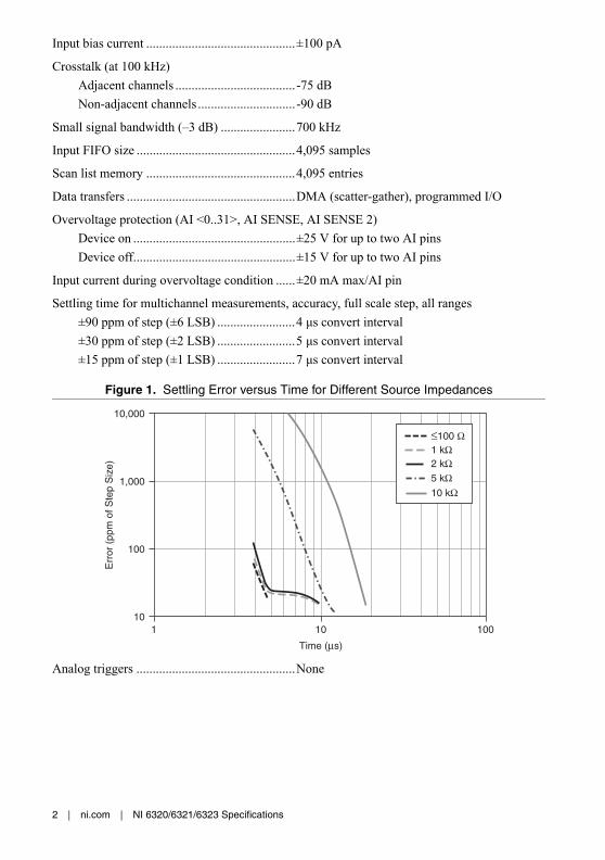
Settling time for multichannel measurements, accuracy, full scale step, all ranges
±90 ppm of step (±6 LSB) ........................4 μs convert interval
±30 ppm of step (±2 LSB) ........................5 μs convert interval
±15 ppm of step (±1 LSB) ........................7 μs convert interval
Figure 1. Settling Error versus Time for Different Source Impedances
Analog triggers .................................................None
Err
or (
ppm
of S
tep
Siz
e)
100
100
1,000
1 10
Time (μs)
10,000
10
≤100 Ω1 kΩ2 kΩ5 kΩ10 kΩ
NI 6320/6321/6323 S
pecifications|
© N
ational Instruments
|3
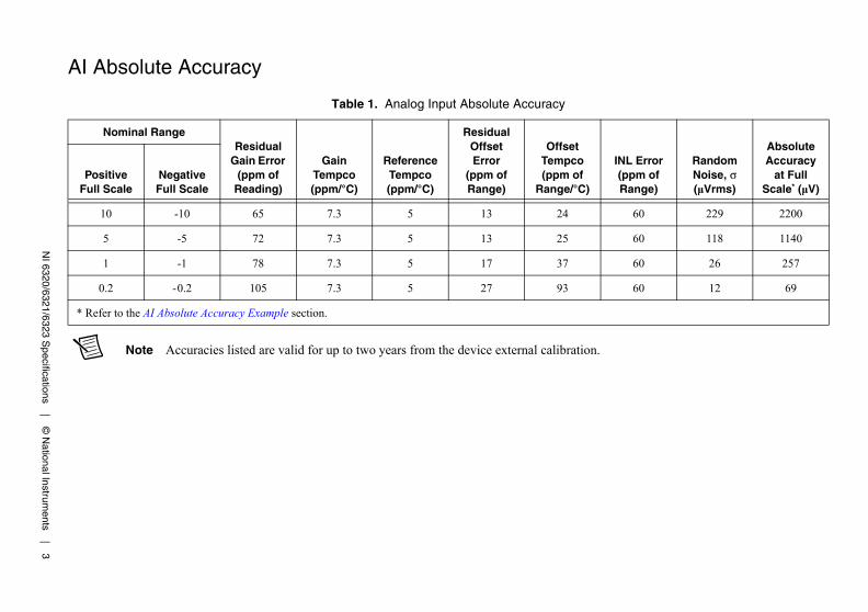
AI Absolute Accuracy
Note Accuracies listed are valid for up to two years from the device external calibration.
Table 1. Analog Input Absolute Accuracy
Nominal RangeResidual
Gain Error (ppm of
Reading)
Gain Tempco (ppm/°C)
Reference Tempco (ppm/°C)
Residual Offset Error
(ppm of Range)
Offset Tempco (ppm of
Range/°C)
INL Error (ppm of Range)
Random Noise, σ (μVrms)
Absolute Accuracy
at Full Scale* (μV)
Positive Full Scale
Negative Full Scale
10 -10 65 7.3 5 13 24 60 229 2200
5 -5 72 7.3 5 13 25 60 118 1140
1 -1 78 7.3 5 17 37 60 26 257
0.2 -0.2 105 7.3 5 27 93 60 12 69
* Refer to the AI Absolute Accuracy Example section.
4 | ni.com | NI 6320/6321/6323 Specifications
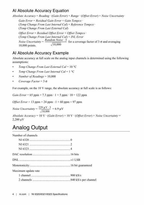
AI Absolute Accuracy EquationAbsolute Accuracy = Reading · (Gain Error) + Range · (Offset Error) + Noise Uncertainty
Gain Error = Residual Gain Error + Gain Tempco · (Temp Change From Last Internal Cal) + Reference Tempco · (Temp Change From Last External Cal)Offset Error = Residual Offset Error + Offset Tempco · (Temp Change From Last Internal Cal) + INL ErrorNoise Uncertainty = for a coverage factor of 3 σ and averaging 10,000 points.
AI Absolute Accuracy ExampleAbsolute accuracy at full scale on the analog input channels is determined using the following assumptions:
• Temp Change From Last External Cal = 10 °C
• Temp Change From Last Internal Cal = 1 °C
• Number of Readings = 10,000
• Coverage Factor = 3 σ
For example, on the 10 V range, the absolute accuracy at full scale is as follows:
Gain Error = 65 ppm + 7.3 ppm · 1 + 5 ppm · 10 = 122 ppm
Offset Error = 13 ppm + 24 ppm · 1 + 60 ppm = 97 ppm
Noise Uncertainty = = 6.9 μV
Absolute Accuracy = 10 V · (Gain Error) + 10 V · (Offset Error) + Noise Uncertainty = 2,200 μV
Analog OutputNumber of channels
NI 6320 .....................................................0
NI 6321 .....................................................2
NI 6323 .....................................................4
DAC resolution .................................................16 bits
DNL ..................................................................±1 LSB
Monotonicity.....................................................16 bit guaranteed
Maximum update rate
1 channel ...................................................900 kS/s
2 channels .................................................840 kS/s per channel
Random Noise 3⋅10,000
------------------------------------------
229 μV 3⋅10,000
--------------------------
NI 6320/6321/6323 Specifications | © National Instruments | 5
3 channels ................................................. 775 kS/s per channel
4 channels ................................................. 719 kS/s per channel
Timing accuracy ............................................... 50 ppm of sample rate
Timing resolution.............................................. 10 ns
Output range ..................................................... ±10 V
Output coupling ................................................ DC
Output impedance............................................. 0.2 Ω
Output current drive.......................................... ±5 mA
Overdrive protection......................................... ±15 V
Overdrive current.............................................. 15 mA
Power-on state .................................................. ±20 mV
Power-on/off glitch ........................................... 2 V for 500 ms
Output FIFO size .............................................. 8,191 samples shared among channels used
Data transfers .................................................... DMA (scatter-gather), programmed I/O
AO waveform modes........................................ Non-periodic waveform, periodic waveform regeneration mode from onboard FIFO, periodic waveform regeneration from host buffer including dynamic update
Settling time, full scale step,
15 ppm (1 LSB) ................................................ 6 μs
Slew rate ........................................................... 15 V/μs
Glitch energy
Magnitude................................................. 100 mV
Duration .................................................... 2.6 μs
6|
ni.com|
NI 6320/6321/6323 S
pecifications
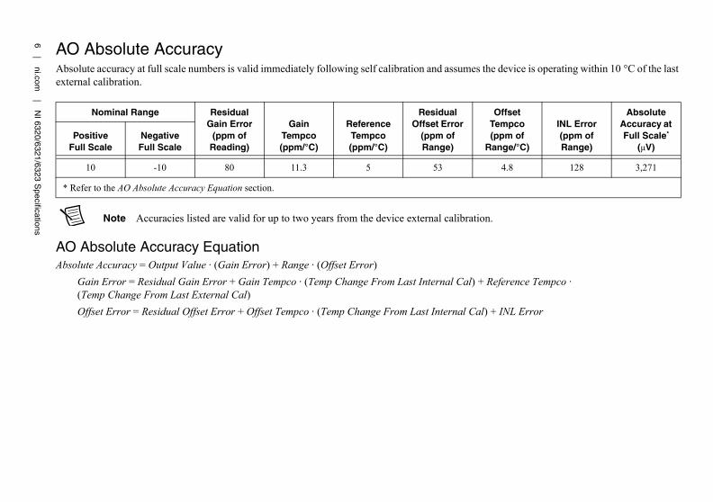
AO Absolute AccuracyAbsolute accuracy at full scale numbers is valid immediately following self calibration and assumes the device is operating within 10 °C of the last external calibration.
Note Accuracies listed are valid for up to two years from the device external calibration.
AO Absolute Accuracy EquationAbsolute Accuracy = Output Value · (Gain Error) + Range · (Offset Error)
Gain Error = Residual Gain Error + Gain Tempco · (Temp Change From Last Internal Cal) + Reference Tempco · (Temp Change From Last External Cal)Offset Error = Residual Offset Error + Offset Tempco · (Temp Change From Last Internal Cal) + INL Error
Nominal Range Residual Gain Error
(ppm of Reading)
Gain Tempco (ppm/°C)
Reference Tempco (ppm/°C)
Residual Offset Error
(ppm of Range)
Offset Tempco (ppm of
Range/°C)
INL Error (ppm of Range)
Absolute Accuracy at Full Scale*
(μV)Positive
Full ScaleNegative Full Scale
10 -10 80 11.3 5 53 4.8 128 3,271
* Refer to the AO Absolute Accuracy Equation section.
NI 6320/6321/6323 Specifications | © National Instruments | 7
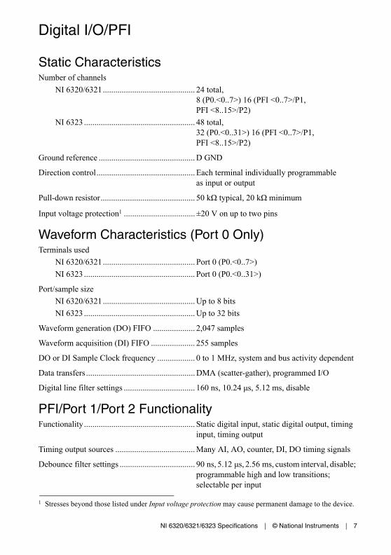
Digital I/O/PFI
Static CharacteristicsNumber of channels
NI 6320/6321............................................ 24 total, 8 (P0.<0..7>) 16 (PFI <0..7>/P1, PFI <8..15>/P2)
NI 6323 ..................................................... 48 total, 32 (P0.<0..31>) 16 (PFI <0..7>/P1, PFI <8..15>/P2)
Ground reference .............................................. D GND
Direction control............................................... Each terminal individually programmable as input or output
Pull-down resistor............................................. 50 kΩ typical, 20 kΩ minimum
Input voltage protection1 .................................. ±20 V on up to two pins
Waveform Characteristics (Port 0 Only)Terminals used
NI 6320/6321............................................ Port 0 (P0.<0..7>)
NI 6323 ..................................................... Port 0 (P0.<0..31>)
Port/sample size
NI 6320/6321............................................ Up to 8 bits
NI 6323 ..................................................... Up to 32 bits
Waveform generation (DO) FIFO .................... 2,047 samples
Waveform acquisition (DI) FIFO ..................... 255 samples
DO or DI Sample Clock frequency .................. 0 to 1 MHz, system and bus activity dependent
Data transfers .................................................... DMA (scatter-gather), programmed I/O
Digital line filter settings .................................. 160 ns, 10.24 μs, 5.12 ms, disable
PFI/Port 1/Port 2 FunctionalityFunctionality ..................................................... Static digital input, static digital output, timing
input, timing output
Timing output sources ...................................... Many AI, AO, counter, DI, DO timing signals
Debounce filter settings .................................... 90 ns, 5.12 μs, 2.56 ms, custom interval, disable; programmable high and low transitions; selectable per input
1 Stresses beyond those listed under Input voltage protection may cause permanent damage to the device.
8 | ni.com | NI 6320/6321/6323 Specifications
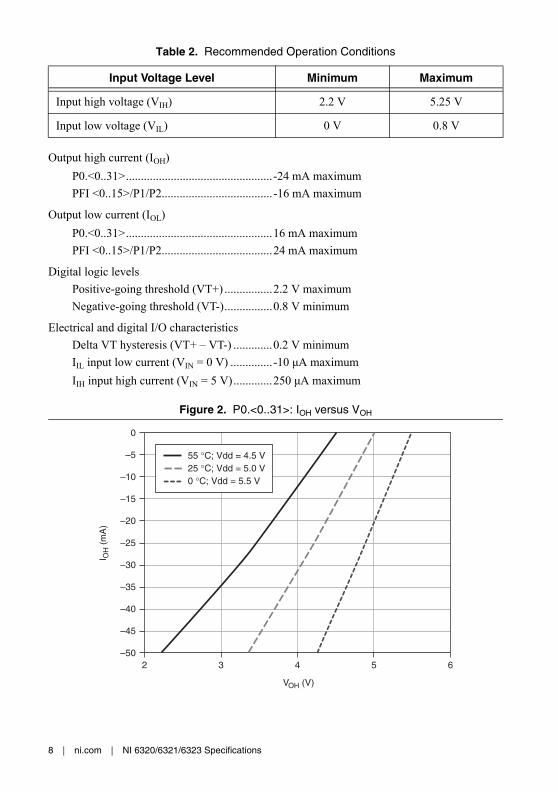
Output high current (IOH)
P0.<0..31>.................................................-24 mA maximum
PFI <0..15>/P1/P2.....................................-16 mA maximum
Output low current (IOL)
P0.<0..31>.................................................16 mA maximum
PFI <0..15>/P1/P2.....................................24 mA maximum
Digital logic levels
Positive-going threshold (VT+) ................2.2 V maximum
Negative-going threshold (VT-)................0.8 V minimum
Electrical and digital I/O characteristics
Delta VT hysteresis (VT+ – VT-) .............0.2 V minimum
IIL input low current (VIN = 0 V) ..............-10 μA maximum
IIH input high current (VIN = 5 V).............250 μA maximum
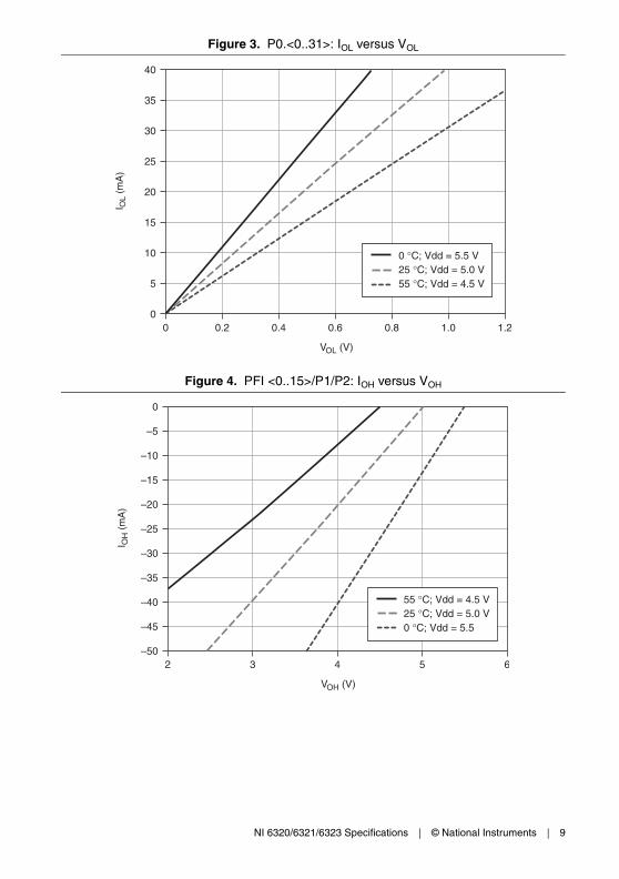
Figure 2. P0.<0..31>: IOH versus VOH
Table 2. Recommended Operation Conditions
Input Voltage Level Minimum Maximum
Input high voltage (VIH) 2.2 V 5.25 V
Input low voltage (VIL) 0 V 0.8 V
I OH
(m
A)
6
–30
–5
–10
–15
–20
–25
–35
–40
–45
2 3 4 5
VOH (V)
0
–50
55 °C; Vdd = 4.5 V25 °C; Vdd = 5.0 V0 °C; Vdd = 5.5 V
NI 6320/6321/6323 Specifications | © National Instruments | 9
Figure 3. P0.<0..31>: IOL versus VOL
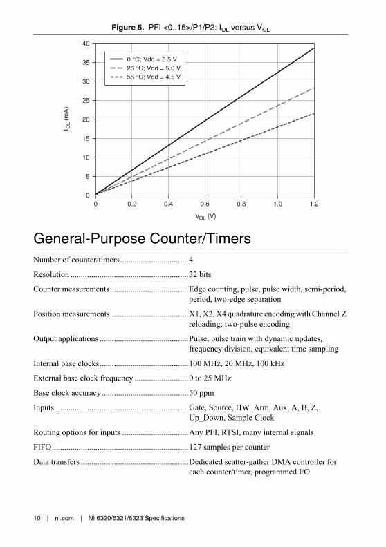
Figure 4. PFI <0..15>/P1/P2: IOH versus VOH
1.0
I OL
(mA
)
1.2
15
35
30
25
20
10
5
0 0.40.2 0.6 0.8
VOL (V)
40
0
0 °C; Vdd = 5.5 V25 °C; Vdd = 5.0 V55 °C; Vdd = 4.5 V
5
I OH
(m
A)
–30
–5
–10
–15
–20
–25
–35
–40
–45
2 3 4
VOH (V)
0
–506
55 °C; Vdd = 4.5 V25 °C; Vdd = 5.0 V0 °C; Vdd = 5.5
10 | ni.com | NI 6320/6321/6323 Specifications
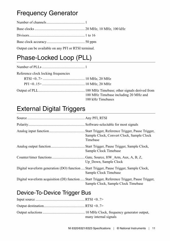
Figure 5. PFI <0..15>/P1/P2: IOL versus VOL
General-Purpose Counter/TimersNumber of counter/timers .................................4
Resolution .........................................................32 bits
Counter measurements......................................Edge counting, pulse, pulse width, semi-period, period, two-edge separation
Position measurements .....................................X1, X2, X4 quadrature encoding with Channel Z reloading; two-pulse encoding
Output applications ...........................................Pulse, pulse train with dynamic updates, frequency division, equivalent time sampling
Internal base clocks...........................................100 MHz, 20 MHz, 100 kHz
External base clock frequency ..........................0 to 25 MHz
Base clock accuracy..........................................50 ppm
Inputs ................................................................Gate, Source, HW_Arm, Aux, A, B, Z, Up_Down, Sample Clock
Routing options for inputs ................................Any PFI, RTSI, many internal signals
FIFO..................................................................127 samples per counter
Data transfers ....................................................Dedicated scatter-gather DMA controller for each counter/timer, programmed I/O
1.0
I OL
(mA
)
1.2
15
35
30
25
20
10
5
0 0.40.2 0.6 0.8
VOL (V)
40
0
0 °C; Vdd = 5.5 V25 °C; Vdd = 5.0 V55 °C; Vdd = 4.5 V
NI 6320/6321/6323 Specifications | © National Instruments | 11
Frequency GeneratorNumber of channels.......................................... 1
Base clocks ....................................................... 20 MHz, 10 MHz, 100 kHz
Divisors............................................................. 1 to 16
Base clock accuracy.......................................... 50 ppm
Output can be available on any PFI or RTSI terminal.
Phase-Locked Loop (PLL)Number of PLLs ............................................... 1
Reference clock locking frequencies
RTSI <0..7> .............................................. 10 MHz, 20 MHz
PFI <0..15>............................................... 10 MHz, 20 MHz
Output of PLL................................................... 100 MHz Timebase; other signals derived from 100 MHz Timebase including 20 MHz and 100 kHz Timebases
External Digital TriggersSource ............................................................... Any PFI, RTSI
Polarity.............................................................. Software-selectable for most signals
Analog input function....................................... Start Trigger, Reference Trigger, Pause Trigger, Sample Clock, Convert Clock, Sample Clock Timebase
Analog output function..................................... Start Trigger, Pause Trigger, Sample Clock, Sample Clock Timebase
Counter/timer functions.................................... Gate, Source, HW_Arm, Aux, A, B, Z, Up_Down, Sample Clock
Digital waveform generation (DO) function .... Start Trigger, Pause Trigger, Sample Clock, Sample Clock Timebase
Digital waveform acquisition (DI) function ..... Start Trigger, Reference Trigger, Pause Trigger, Sample Clock, Sample Clock Timebase
Device-To-Device Trigger BusInput source ...................................................... RTSI <0..7>
Output destination............................................. RTSI <0..7>
Output selections .............................................. 10 MHz Clock, frequency generator output, many internal signals
12 | ni.com | NI 6320/6321/6323 Specifications
Debounce filter settings ....................................90 ns, 5.12 μs, 2.56 ms, custom interval, disable; programmable high and low transitions; selectable per input
Bus InterfaceForm factor .......................................................x1 PCI Express, specification v1.1 compliant
Slot compatibility..............................................x1, x4, x8, and x16 PCI Express slots1
DMA channels ..................................................8, analog input, analog output, digital input, digital output, counter/timer 0, counter/timer 1, counter/timer 2, counter/timer 3
Power RequirementsWithout disk drive power connector installed
+3.3 V .......................................................1.4 W
+12 V ........................................................8.6 W
With disk drive power connector installed
+3.3 V .......................................................1.4 W
+12 V ........................................................3 W
+5 V ..........................................................15 W
Current Limits
Caution Exceeding the current limits may cause unpredictable behavior by the device and/or PC.
Without disk drive power connector installedP0/PFI/P1/P2 and +5 V terminals combined ....1 A max
With disk drive power connector installed
+5 V terminal (connector 0)......................1 A max2
+5 V terminal (connector 1)......................1 A max2
P0/PFI/P1/P2 combined............................1 A max
1 Some motherboards reserve the x16 slot for graphics use. For PCI Express guidelines, refer to ni.com/pciexpress.
2 Has a self-resetting fuse that opens when current exceeds this specification.
NI 6320/6321/6323 Specifications | © National Instruments | 13
CalibrationRecommended warm-up time........................... 15 minutes
Calibration interval ........................................... 2 years
Physical RequirementsPrinted circuit board dimensions ...................... 9.9 × 16.8 cm (3.9 × 6.6 in.) (half-length)
Weight
NI 6320/6321............................................ 104 g (3.6 oz)
NI 6323 ..................................................... 114 g (4.0 oz)
I/O connector
NI 6320/6321............................................ 1 68-pin VHDCI
NI 6323 ..................................................... 2 68-pin VHDCI
Disk drive power connector.............................. Standard ATX peripheral connector (not serial ATA)
Clean the hardware with a soft, nonmetallic brush.
Maximum Working Voltage1
Caution The protection provided by the DAQ device can be impaired if it is used in a manner not described in the X Series User Manual.
Channel to earth................................................ 11 V, Measurement Category I
Note Measurement Categories CAT I and CAT O (Other) are equivalent. These test and measurement circuits are not intended for direct connection to the MAINs building installations of Measurement Categories CAT II, CAT III, or CAT IV.
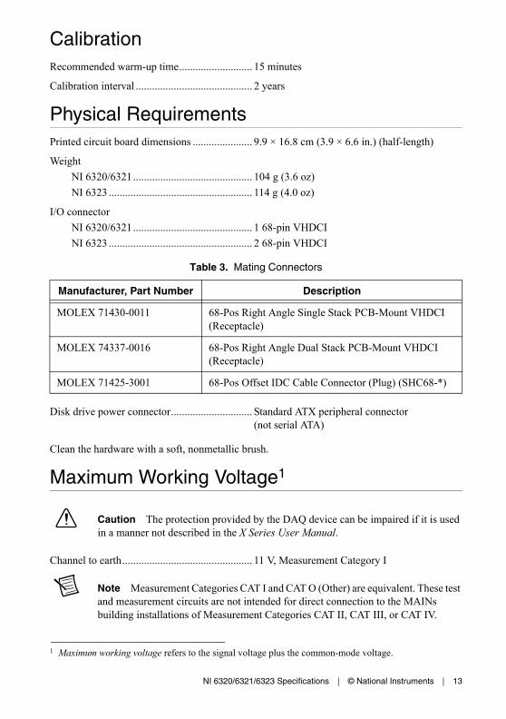
Table 3. Mating Connectors
Manufacturer, Part Number Description
MOLEX 71430-0011 68-Pos Right Angle Single Stack PCB-Mount VHDCI (Receptacle)
MOLEX 74337-0016 68-Pos Right Angle Dual Stack PCB-Mount VHDCI (Receptacle)
MOLEX 71425-3001 68-Pos Offset IDC Cable Connector (Plug) (SHC68-*)
1 Maximum working voltage refers to the signal voltage plus the common-mode voltage.
14 | ni.com | NI 6320/6321/6323 Specifications
EnvironmentalOperating temperature ......................................0 to 50 °C
Storage temperature ..........................................-40 to 70 °C
Operating humidity ...........................................10 to 90% RH, noncondensing
Storage humidity ...............................................5 to 95% RH, noncondensing
Pollution Degree ...............................................2
Maximum altitude.............................................2,000 m
Indoor use only.
SafetyThis product meets the requirements of the following standards of safety for electrical equipment for measurement, control, and laboratory use:
• IEC 61010-1, EN 61010-1
• UL 61010-1, CSA 61010-1
Note For UL and other safety certifications, refer to the product label or the Online Product Certification section.
Electromagnetic CompatibilityThis product meets the requirements of the following EMC standards for electrical equipment for measurement, control, and laboratory use:
• EN 61326-1 (IEC 61326-1): Class A emissions; Basic immunity
• EN 55011 (CISPR 11): Group 1, Class A emissions
• AS/NZS CISPR 11: Group 1, Class A emissions
• FCC 47 CFR Part 15B: Class A emissions
• ICES-001: Class A emissions
Note In the United States (per FCC 47 CFR), Class A equipment is intended for use in commercial, light-industrial, and heavy-industrial locations. In Europe, Canada, Australia and New Zealand (per CISPR 11) Class A equipment is intended for use only in heavy-industrial locations.
Note Group 1 equipment (per CISPR 11) is any industrial, scientific, or medical equipment that does not intentionally generate radio frequency energy for the treatment of material or inspection/analysis purposes.
Note For EMC declarations and certifications, and additional information, refer to the Online Product Certification section.
NI 6320/6321/6323 Specifications | © National Instruments | 15
CE ComplianceThis product meets the essential requirements of applicable European Directives as follows:
• 2006/95/EC; Low-Voltage Directive (safety)
• 2004/108/EC; Electromagnetic Compatibility Directive (EMC)
Online Product CertificationTo obtain product certifications and the Declaration of Conformity (DoC) for this product, visit ni.com/certification, search by model number or product line, and click the appropriate link in the Certification column.
Environmental ManagementNI is committed to designing and manufacturing products in an environmentally responsible manner. NI recognizes that eliminating certain hazardous substances from our products is beneficial to the environment and to NI customers.
For additional environmental information, refer to the Minimize Our Environmental Impact web page at ni.com/environment. This page contains the environmental regulations and directives with which NI complies, as well as other environmental information not included in this document.
Waste Electrical and Electronic Equipment (WEEE)EU Customers At the end of the product life cycle, all products must be sent to a WEEE recycling center. For more information about WEEE recycling centers, National Instruments WEEE initiatives, and compliance with WEEE Directive 2002/96/EC on Waste and Electronic Equipment, visit ni.com/environment/ weee.
Contact InformationNational Instruments corporate headquarters11500 North Mopac Expressway, Austin, Texas, 78759-3504512 795 8248ni.com/niglobal
RoHSNational Instruments
(RoHS) National Instruments RoHS ni.com/environment/rohs_china (For information about China RoHS compliance, go to ni.com/environment/rohs_china.)
16 | ni.com | NI 6320/6321/6323 Specifications
Figure 6. NI PCIe-6320 Pinout
CO
NN
EC
TOR
0(A
I 0-1
5)
D GND
D GND
PFI 8/P2.0
PFI 7/P1.7
PFI 15/P2.7
PFI 13/P2.5
PFI 4/P1.4
PFI 3/P1.3
PFI 2/P1.2
D GND
PFI 10/P2.2
PFI 11/P2.3
P0.3
P0.7
P0.2
D GND
P0.5
P0.0
D GND
NC
NC
AI GND
AI 7 (AI 7+)
AI 14 (AI 6–)
AI GND
AI 5 (AI 5+)
AI 12 (AI 4–)
AI SENSE
AI 11 (AI 3–)
AI GND
AI 2 (AI 2+)
AI 9 (AI 1–)
AI GND
AI 0 (AI 0+)
PFI 14/P2.6
PFI 9/P2.1
D GND
PFI 5/P1.5
D GND
+5 V
D GND
PFI 12/P2.4
PFI 6/P1.6
PFI 1/P1.1
PFI 0/P1.0
D GND
D GND
+5 V
D GND
P0.6
P0.1
D GND
P0.4
NC
NC
NC
AI 15 (AI 7–)
AI GND
AI 6 (AI 6+)
AI 13 (AI 5–)
AI GND
AI 4 (AI 4+)
AI GND
AI 3 (AI 3+)
AI 10 (AI 2–)
AI GND
AI 1 (AI 1+)
AI 8 (AI 0–)68 34
67 33
66 32
65 31
64 30
63 29
62 28
61 27
60 26
59 25
58 24
57 23
56 22
55 21
54 20
53 19
52 18
51 17
50 16
49 15
48 14
47 13
46 12
45 11
44 10
43 9
42 8
41 7
40 6
39 5
38 4
37 3
36 2
35 1
TERMINAL 34TERMINAL 68
TERMINAL 1TERMINAL 35
NC = No Connect

NI 6320/6321/6323 Specifications | © National Instruments | 17
Figure 7. NI PCIe-6321 Pinout
CO
NN
EC
TOR
0(A
I 0-1
5)
D GND
D GND
PFI 8/P2.0
PFI 7/P1.7
PFI 15/P2.7
PFI 13/P2.5
PFI 4/P1.4
PFI 3/P1.3
PFI 2/P1.2
D GND
PFI 10/P2.2
PFI 11/P2.3
P0.3
P0.7
P0.2
D GND
P0.5
P0.0
D GND
AO GND
AO GND
AI GND
AI 7 (AI 7+)
AI 14 (AI 6–)
AI GND
AI 5 (AI 5+)
AI 12 (AI 4–)
AI SENSE
AI 11 (AI 3–)
AI GND
AI 2 (AI 2+)
AI 9 (AI 1–)
AI GND
AI 0 (AI 0+)
PFI 14/P2.6
PFI 9/P2.1
D GND
PFI 5/P1.5
D GND
+5 V
D GND
PFI 12/P2.4
PFI 6/P1.6
PFI 1/P1.1
PFI 0/P1.0
D GND
D GND
+5 V
D GND
P0.6
P0.1
D GND
P0.4
NC
AO 1
AO 0
AI 15 (AI 7–)
AI GND
AI 6 (AI 6+)
AI 13 (AI 5–)
AI GND
AI 4 (AI 4+)
AI GND
AI 3 (AI 3+)
AI 10 (AI 2–)
AI GND
AI 1 (AI 1+)
AI 8 (AI 0–)68 34
67 33
66 32
65 31
64 30
63 29
62 28
61 27
60 26
59 25
58 24
57 23
56 22
55 21
54 20
53 19
52 18
51 17
50 16
49 15
48 14
47 13
46 12
45 11
44 10
43 9
42 8
41 7
40 6
39 5
38 4
37 3
36 2
35 1
TERMINAL 34TERMINAL 68
TERMINAL 1TERMINAL 35
NC = No Connect
© 2009–2013 National Instruments. All rights reserved.
370785D-01 Apr13
Refer to the NI Trademarks and Logo Guidelines at ni.com/trademarks for more information on National Instruments trademarks. Other product and company names mentioned herein are trademarks or trade names of their respective companies. For patents covering National Instruments products/technology, refer to the appropriate location: Help»Patents in your software, the patents.txt file on your media, or the National Instruments Patents Notice at ni.com/patents. You can find information about end-user license agreements (EULAs) and third-party legal notices in the readme file for your NI product. Refer to the Export Compliance Information at ni.com/legal/export-compliance for the National Instruments global trade compliance policy and how to obtain relevant HTS codes, ECCNs, and other import/export data.
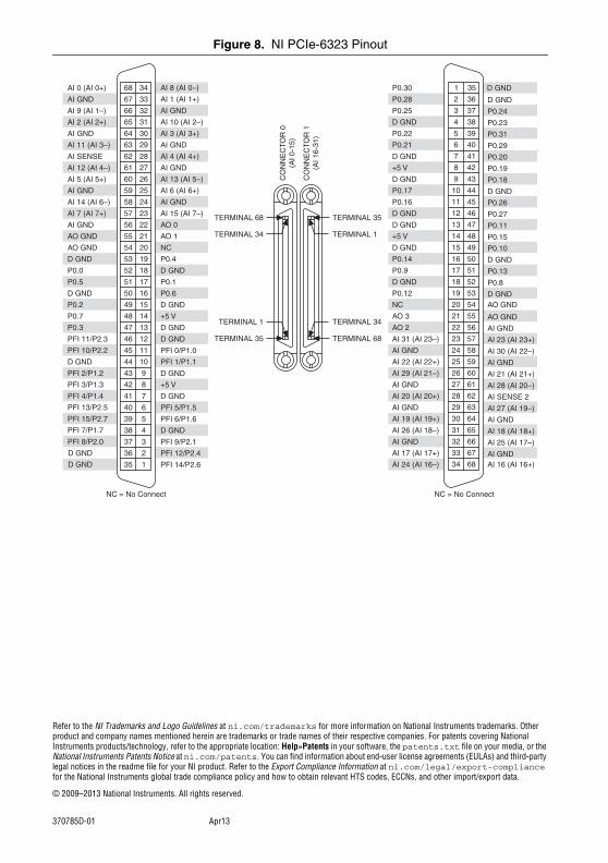
Figure 8. NI PCIe-6323 Pinout
D GND
D GND
PFI 8/P2.0
PFI 7/P1.7
PFI 15/P2.7
PFI 13/P2.5
PFI 4/P1.4
PFI 3/P1.3
PFI 2/P1.2
D GND
PFI 10/P2.2
PFI 11/P2.3
P0.3
P0.7
P0.2
D GND
P0.5
P0.0
D GND
AO GND
AO GND
AI GND
AI 7 (AI 7+)
AI 14 (AI 6–)
AI GND
AI 5 (AI 5+)
AI 12 (AI 4–)
AI SENSE
AI 11 (AI 3–)
AI GND
AI 2 (AI 2+)
AI 9 (AI 1–)
AI GND
AI 0 (AI 0+)
PFI 14/P2.6
PFI 9/P2.1
D GND
PFI 5/P1.5
D GND
+5 V
D GND
PFI 12/P2.4
PFI 6/P1.6
PFI 1/P1.1
PFI 0/P1.0
D GND
D GND
+5 V
D GND
P0.6
P0.1
D GND
P0.4
NC
AO 1
AO 0
AI 15 (AI 7–)
AI GND
AI 6 (AI 6+)
AI 13 (AI 5–)
AI GND
AI 4 (AI 4+)
AI GND
AI 3 (AI 3+)
AI 10 (AI 2–)
AI GND
AI 1 (AI 1+)
AI 8 (AI 0–)68 34
67 33
66 32
65 31
64 30
63 29
62 28
61 27
60 26
59 25
58 24
57 23
56 22
55 21
54 20
53 19
52 18
51 17
50 16
49 15
48 14
47 13
46 12
45 11
44 10
43 9
42 8
41 7
40 6
39 5
38 4
37 3
36 2
35 1 AI 24 (AI 16–)
AI 17 (AI 17+)
AI GND
AI 26 (AI 18–)
AI 19 (AI 19+)
AI GND
AI 20 (AI 20+)
AI GND
AI 29 (AI 21–)
AI 22 (AI 22+)
AI GND
AI 31 (AI 23–)
AO 2
AO 3
NC
P0.12
D GND
P0.9
P0.14
D GND
+5 V
D GND
D GND
P0.16
P0.17
D GND
+5 V
D GND
P0.21
P0.22
D GND
P0.25
P0.28
P0.30
AI 16 (AI 16+)
AI 25 (AI 17–)
AI 18 (AI 18+)
AI 27 (AI 19–)
AI SENSE 2
AI 28 (AI 20–)
AI 21 (AI 21+)
AI GND
AI GND
AI GND
AI 30 (AI 22–)
AI 23 (AI 23+)
AI GND
AO GND
AO GNDD GND
P0.8
P0.13
D GND
P0.10
P0.15
P0.11
P0.27
P0.26
D GND
P0.18
P0.19
P0.20
P0.29
P0.31
P0.23
P0.24
D GND
D GND1 35
2 36
3 37
4 38
5 39
6 40
7 41
8 42
9 43
10 44
11 45
12 46
13 47
14 48
15 49
16 50
17 51
18 52
19 53
20 54
21 55
22 56
23 57
24 58
25 59
26 60
27 61
28 62
29 63
30 64
31 65
32 66
33 67
34 68
TERMINAL 34
TERMINAL 68
TERMINAL 35
TERMINAL 1
TERMINAL 35
TERMINAL 1
TERMINAL 34
TERMINAL 68
NC = No Connect NC = No Connect
CO
NN
EC
TOR
0(A
I 0-1
5)
CO
NN
EC
TOR
1(A
I 16-
31)